

Page 1

GM47/GM48
Product Photo/Illustration
Page 2

The product described in this manual conforms to the Radio and Telecommunications
Terminal Equipment (R&TTE) directive 99/5/EC with requirements covering EMC
directive 89/336/EEC and Low Voltage directive 73/23/EEC. The product fulfils the
requirements according to 3GPP TS 51.010-1, EN 301 489-7 and EN60950.
SAR statement: This product is intended to be used with the antenna or other
radiating element at least 20cm away from any part of the human body.
The information contained in this document is the proprietary information of
Sony Ericsson Mobile Communications International. The contents are
confidential and any disclosure to persons other than the officers, employees, agents
or subcontractors of the owner or licensee of this document, without the prior written
consent of Sony Ericsson Mobile Communications International, is strictly
prohibited. Further, no portion of this publication may be reproduced, stored in a
retrieval system, or transmitted in any form or by any means, electronic or
mechanical, including photocopying and recording, without the prior written consent
of Sony Ericsson Mobile Communications International, the copyright holder.
First edition (April 2002)
Second edition (August 2002)
Third edition (January 2003)
Sony Ericsson Mobile Communications International publishes this manual
without making any warranty as to the content contained herein. Further
Sony Ericsson Mobile Communications International reserves the right to make
modifications, additions and deletions to this manual due to typographical errors,
inaccurate information, or improvements to programs and/or equipment at any time
and without notice. Such changes will, nevertheless be incorporated into new editions
of this manual.
All rights reserved.
© Sony Ericsson Mobile Communications International, 2003
Publication number: LZT 123 7263 R1C
Printed in UK
Page 3

Contents
Part 1: Overview................................................................................................. 11
1. Introduction............................................................................................................ 13
1.1 Target Users ......................................................................................... 13
1.2 Prerequisites ......................................................................................... 13
1.3 Manual Structure ......................................................................................... 13
2. GM47/GM48 Modules ........................................................................................... 15
2.1 About the GM47/GM48 Family .................................................................. 15
2.2 GM47 in a Communication System............................................................. 15
2.3 Features ......................................................................................... 17
2.3.1 Types of Mobile Station .................................................................. 17
2.3.2 Short Message Service .................................................................... 18
2.3.3 Voice Calls...................................................................................... 18
2.3.4 Data................................................................................................. 18
2.3.5 SIM Card......................................................................................... 19
2.3.6 Average Power Consumption ......................................................... 19
2.3.7 Other Features ................................................................................ 19
2.4 Service and Support ..................................................................................... 19
2.4.1 Web Pages....................................................................................... 19
2.4.2 Integrator’s Manual........................................................................ 19
2.4.3 Developer’s Kit ...............................................................................20
2.5 Precautions ......................................................................................... 20
3. Abbreviations .........................................................................................................21
Part 2: Developer’s Kit ....................................................................................... 23
1. Introduction............................................................................................................ 25
1.1 Overview ......................................................................................... 25
1.2 Contents of the Kit ....................................................................................... 25
1.3 General Functioning of the Kit .................................................................... 26
2. Using the Developer’s Kit...................................................................................... 29
2.1 Start up Check List....................................................................................... 30
2.2 Developer’s Board Overlay.......................................................................... 31
2.3 Jumpers, Switches and Connectors.............................................................. 32
2.4 System Connector Pin Assignments ............................................................ 36
Part 3: Integrating the Module............................................................................ 37
1. Mechanical Description ......................................................................................... 39
1.1 Interface Description.................................................................................... 39
1.2 Physical Dimensions .................................................................................... 40
LZT 123 7263 R1C
3
Page 4

GM47/GM48 INTEGRATOR’S MANUAL
2. System Connector Interface ..................................................................................41
2.1 Overview .......................................................................................... 41
2.2 General Electrical and Logical Characteristics ............................................ 44
2.2.1 General Protection Requirements ...................................................44
2.3 Grounds .......................................................................................... 45
2.3.1 Analogue Ground - AGND ..............................................................45
2.3.2 Digital Ground - DGND..................................................................45
2.4 VCC - Regulated Power Supply Input ......................................................... 45
2.5 ON/OFF and External Power Signal ............................................................ 46
2.5.1 Switching the module ON and OFF ................................................46
2.5.2 VIO - 2.75V Supply..........................................................................47
2.6 Analogue Audio .......................................................................................... 48
2.6.1 Audio To Mobile Station - ATMS ....................................................48
2.6.2 Audio From Mobile Station - AFMS ...............................................49
2.6.3 Microphone Signals.........................................................................50
2.6.4 Speaker Signals ...............................................................................51
2.7 PCM Digital Audio....................................................................................... 52
2.7.1 PCM Data Format...........................................................................53
2.8 Serial Data Interfaces.................................................................................... 55
2.8.1 UART1 (RS232) - RD, TD, RTS, CTS, DTR, DCD and RI..............55
2.8.2 Serial Data Signals - RD, TD..........................................................56
2.8.3 Control Signals - RTS, CTS, DTR, DCD, RI ...................................56
2.8.4 UART2 - TD2, RD2 .........................................................................58
2.8.5 UART3 - TD3, RD3 (designated for future use)..............................59
2.9 SIM Card Related Signals ............................................................................ 59
2.9.1 SIM Detection - SIMPRESENCE ....................................................60
2.10 Service/Programming................................................................................... 61
2.11 Buzzer .......................................................................................... 61
2.12 LED .......................................................................................... 61
2.13 General Purpose Digital I/O Ports................................................................ 62
2.14 General Purpose Analogue I/O Ports............................................................ 63
2.14.1 Digital to Analogue Converter - DAC.............................................63
2.14.2 Analogue to Digital Converters 1, 2 and 3 - ADCx ........................64
2.15 External I 2C Serial Control Bus .................................................................. 65
2.16 TX_ON - Burst Transmission....................................................................... 65
2.17 Real Time Clock .......................................................................................... 66
3. Antenna Connector ................................................................................................68
4. Hints for Integrating the Module..........................................................................69
4.1 Safety Advice and Precautions ..................................................................... 69
4.1.1 General............................................................................................69
4.1.2 SIM Card .........................................................................................69
4.1.3 Antenna............................................................................................70
4.2 Installation of the Module............................................................................. 70
4.2.1 Where to Install the Module ............................................................70
4.2.2 How to Install the Module...............................................................71
4.3 Antenna .......................................................................................... 72
4
LZT 123 7263 R1C
Page 5

4.3.1 General ........................................................................................... 72
4.3.2 Antenna Type .................................................................................. 73
4.3.3 Antenna Placement .........................................................................73
4.3.4 The Antenna Cable.......................................................................... 73
4.3.5 Possible Communication Disturbances .......................................... 74
5. Technical Data........................................................................................................ 75
6. Declaration of Conformity .................................................................................... 77
7. FCC Certificate ...................................................................................................... 78
Part 4: Using AT Commands.............................................................................. 79
1. Introduction to AT Commands ............................................................................81
1.1 Overview ......................................................................................... 81
1.2 Syntax Description....................................................................................... 81
1.2.1 Conventions..................................................................................... 81
1.2.2 AT Command Syntax....................................................................... 82
1.2.3 AT Response Syntax ........................................................................84
1.3 Error Codes ......................................................................................... 85
1.3.1 +CME ERROR (Mobile Equipment Error Code)........................... 85
1.3.2 +CMS ERROR (Message Service Failure Result Code) ................ 86
1.4 Examples on How to Use the AT Commands ............................................ 87
1.5 SMS Text Mode ......................................................................................... 87
1.6 GPRS Communication................................................................................. 89
2. Call Control ............................................................................................................ 91
2.1 AT+CPIN PIN Control...................................................................... 91
2.2 ATA Answer Incoming Call..................................................... 91
2.3 ATD Dial .................................................................................. 92
2.4 ATH Hang up............................................................................ 94
2.5 ATL Monitor Speaker Loudness.............................................. 94
2.6 ATO Return to Online Data Mode............................................ 95
2.7 ATP Select Pulse Dialling........................................................ 95
2.8 ATT Select Tone Dialling ........................................................ 95
2.9 ATX Call Progress Monitoring Control ................................... 96
2.10 AT+CHUP Hang up Call .................................................................... 96
2.11 AT+CMOD Call Mode ........................................................................ 97
2.12 AT+CVHU Voice Hang-Up................................................................ 98
2.13 AT+VTS DTMF and Tone Generation ........................................... 98
3. Control and Status ...............................................................................................101
3.1 ATQ Result Code Suppression ............................................... 101
3.2 ATS0 Automatic Answer Control............................................ 101
3.3 ATS2 Escape Sequence Character ........................................... 102
3.4 ATS3 Command Line Termination Character ......................... 102
3.5 ATS4 Response Formatting Character..................................... 103
LZT 123 7263 R1C
5
Page 6

GM47/GM48 INTEGRATOR’S MANUAL
3.6 ATS5 Command Line Editing Character (BACKSPACE) ...... 104
3.7 ATS6 Blind Dial Delay Control ............................................... 104
3.8 ATS7 Connection Completion Timeout................................... 105
3.9 ATS8 Comma Dial Modifier Delay Control ............................ 105
3.10 ATS10 Automatic Disconnect Delay Control ............................ 106
3.11 AT*ECAM Ericsson Call Monitoring ............................................... 106
3.12 AT*EDST Ericsson Daylight Saving Time ..................................... 108
3.13 AT*EMAR Ericsson Master Reset .................................................... 109
3.14 AT*EPEE Ericsson Pin Event ......................................................... 110
3.15 AT*ESMM Ericsson Settings Minute Minder................................... 110
3.16 AT+CALA Set Alarm ....................................................................... 111
3.17 AT+CALD Alarm Delete .................................................................. 112
3.18 AT+CCLK Set Clock and Date......................................................... 113
3.19 AT+CEER Extended Error Report ................................................... 114
3.20 AT+CFUN Set Phone Functionality ................................................. 114
3.21 AT+CIND Indicator Control ............................................................ 115
3.22 AT+CLAC List all available AT Commands.................................... 116
3.23 AT+CMEE Mobile Equipment Error ................................................ 116
3.24 AT+CMER Mobile Equipment Event Reporting .............................. 117
3.25 AT+CPAS Phone Activity Status..................................................... 118
3.26 AT+CPIN PIN Control .................................................................... 120
3.27 AT+CPWD Change Password ........................................................... 122
3.28 AT+CR Service Reporting Control.............................................. 124
3.29 AT+CRC Cellular Result Code ...................................................... 124
3.30 AT+CSAS Save Settings .................................................................. 125
3.31 AT+CSQ Signal Strength ............................................................... 126
3.32 AT+CTZU Automatic Time Zone Update........................................ 127
4. Audio......................................................................................................................129
4.1 AT*E2EAMS Ericsson M2M Audio Profile Modification ................... 129
4.2 AT*E2APR M2M Audio Profile Manipulation ................................. 135
4.3 AT*EALR Ericsson Audio Line Request......................................... 137
4.4 AT*EAMS Ericsson Audio Mode Selection..................................... 138
4.5 AT*EARS Ericsson Audio Ring Signal ........................................... 139
4.6 AT*E2PHFB Portable Handsfree Button Sense Enable....................... 140
4.7 AT*ELAM Ericsson Local Audio Mode........................................... 140
4.8 AT*EMIC Ericsson Microphone Mode ........................................... 141
4.9 AT*EMIR Ericsson Music Mute Indication Request ...................... 141
4.10 AT*EPRR Ericsson Personal Ring Type Read ................................ 142
4.11 AT*EPRW Ericsson Personal Ringtype Write ................................. 143
4.12 AT*ERIL Ericsson Ring Level Set ................................................. 145
4.13 AT*ERIN Ericsson Ring Set ........................................................... 146
4.14 AT*ERIP Ericsson Ring Signal Playback Command..................... 147
4.15 AT*ESMA Ericsson Set Message Alert Sound ................................ 148
4.16 AT*ESOM Ericsson Settings Own Melody ...................................... 148
4.17 AT*EXVC Ericsson Set External Volume Control .......................... 150
4.18 ATM Monitor Speaker Control................................................ 151
6
LZT 123 7263 R1C
Page 7

5. Data - CSD/HSCSD.............................................................................................. 153
5.1 AT+CBST Select Bearer Service Type............................................ 153
5.2 AT+CRLP Radio Link Protocol....................................................... 155
6. Data - GPRS .........................................................................................................157
6.1 AT+CGACT PDP Context Activate or Deactivate ............................. 157
6.2 AT+CGATT GPRS Attach or Detach ................................................. 158
6.3 AT+CGDATA Enter Data State ............................................................. 159
6.4 AT+CGDCONT Define PDP Context ...................................................... 160
6.5 AT+CGEREP GPRS Event Reporting.................................................. 162
6.6 AT+CGPADDR Show PDP Address........................................................ 163
6.7 AT+CGQMIN Quality of Service Profile (Minimum Acceptable) ....... 164
6.8 AT+CGQREQ Quality of Service Profile (Requested).......................... 166
6.9 AT+CGREG GPRS Network Registration Status ............................... 169
6.10 AT+CGSMS Select Service for MO SMS Messages .......................... 170
7. Data - HSCSD....................................................................................................... 171
7.1 AT+CHSC HSCSD Current Call Parameters ................................... 171
7.2 AT+CHSD HSCSD Device Parameters ........................................... 172
7.3 AT+CHSN HSCSD Non Transparent Call Configuration ............... 173
7.4 AT+CHSR HSCSD Parameters Report ............................................ 174
7.5 AT+CHSU HSCSD Automatic User Initiated Upgrading................ 175
8. GPS Interoperability ........................................................................................... 177
8.1 AT*EENMEA NMEA (GPS) Mode on UART2 ................................... 177
8.2 AT*E2NMPR Ericsson M2M Set NMEA (GPS) Port Rate.................. 178
9. Fax ......................................................................................................................... 181
9.1 AT*E2FAX Ericsson M2M Fax Comm. Baud Rate Modification.... 181
9.2 Low Level Fax Commands ........................................................................ 182
10. Identification ........................................................................................................183
10.1 AT Attention Command....................................................... 183
10.2 AT&F Set to Factory Defined Configuration............................ 183
10.3 AT&W Store User Profile .......................................................... 183
10.4 AT* List all Supported AT Commands ................................. 184
10.5 AT+CGMI Read MS Manufacturer Identification ........................... 184
10.6 AT+CGMM Read MS Model Identification ...................................... 184
10.7 AT+CGMR Read MS Revision Identification................................... 185
10.8 AT+CGSN Read MS Product Serial Number Identification ............ 186
10.9 AT+GMI Read Manufacturer Identification.................................. 186
10.10 AT+GMM Read Model Identification ............................................. 187
10.11 AT+GMR Read Revision Identification ......................................... 187
10.12 ATI Identification Information.............................................. 188
11. Input/Output ........................................................................................................ 191
11.1 AT*E2IO Ericsson M2M Input/Output Read/Write ...................... 191
LZT 123 7263 R1C
7
Page 8

GM47/GM48 INTEGRATOR’S MANUAL
12. Interface ................................................................................................................197
12.1 AT+CPIN PIN Control .................................................................... 197
12.2 AT&C Circuit 109 (DCD) Control ............................................ 197
12.3 AT&D Circuit 108 (DTR) Response.......................................... 197
12.4 AT&S Circuit 107 (DSR) Response.......................................... 197
12.5 AT+WS46 Mode Selection............................................................... 198
12.6 ATE Command Echo.............................................................. 198
12.7 ATV DCE Response Format................................................... 199
12.8 ATZ Reset to Default Configuration ...................................... 200
12.9 AT+CMUX Switch to 07.10 Multiplex Protocol ............................... 200
12.10 AT+CRES Restore SMS Settings..................................................... 202
12.11 AT+ICF Cable Interface Character Format .................................. 202
12.12 AT+IFC DTE-DCE Local Flow Control ...................................... 203
12.13 AT+ILRR Cable Interface Local Rate Reporting............................ 204
12.14 AT+IPR Cable Interface Port Command...................................... 204
12.15 AT*E2SPI Serial Peripheral Interface.............................................. 205
12.16 AT*E2ESC M2M Escape Sequence Guard Time.............................. 207
13. Network .................................................................................................................209
13.1 AT*E2CD Ericsson M2M Cell Description..................................... 209
13.2 AT*E2EMM Ericsson M2M Engineering Monitoring Mode.............. 211
13.3 AT*E2SPN M2M Service Provider Indication.................................. 217
13.4 AT*EALS Ericsson Request ALS Status......................................... 217
13.5 AT*ECSP Ericsson Customer Service Profile................................. 218
13.6 AT*EPNR Ericsson Read SIM Preferred Network.......................... 219
13.7 AT*EPNW Ericsson Write SIM Preferred Network......................... 220
13.8 AT*E2SSN Ericsson M2M SIM Serial Number ............................... 221
13.9 AT*ESLN Ericsson Set Line Name ................................................. 222
13.10 AT+CIMI Subscriber Identification ................................................ 223
13.11 AT+CLCK Facility Lock .................................................................. 223
13.12 AT+CNUM Subscriber Number......................................................... 225
13.13 AT+COLP Connected Line Identification Presentation................... 226
13.14 AT+COPS Operator Selection.......................................................... 228
13.15 AT+CREG Network Registration ..................................................... 229
13.16 AT*ECPI Ciphering Indicator ........................................................ 230
13.17 AT*E2NBTS Ericsson M2M Neighbour BTS ..................................... 232
14. Phonebook.............................................................................................................235
14.1 AT*E2PBCS Ericsson M2M Phonebook Check Sum ......................... 235
14.2 AT*ESAG Ericsson Add to Group................................................... 235
14.3 AT*ESCG Ericsson Create Group ................................................... 236
14.4 AT*ESCN Ericsson Set Credit Card Number .................................. 237
14.5 AT*ESDG Ericsson Delete Group ................................................... 239
14.6 AT*ESDI Ericsson Delete Group Item ........................................... 239
14.7 AT*ESGR Ericsson Group Read...................................................... 240
14.8 AT*EGIR Ericsson Group Item Read ............................................. 240
14.9 AT*ESIL Ericsson Silence Command............................................ 241
8
LZT 123 7263 R1C
Page 9

14.10 AT*ESNU Ericsson Settings Number.............................................. 242
14.11 AT+CPBF Phonebook Find ............................................................. 243
14.12 AT+CPBR Phonebook Read ............................................................ 243
14.13 AT+CPBS Phone Storage ................................................................ 245
14.14 AT+CPBW Phonebook Write ........................................................... 246
14.15 AT*ECAW Ericsson Callers Allowed Write ................................... 247
14.16 AT*ECAR Ericsson Callers Allowed Read ..................................... 248
15. Short Message Services - Point to Point............................................................. 251
15.1 AT+CPIN PIN Control.................................................................... 251
15.2 AT+CGSMS Select Service for MO SMS Messages.......................... 251
15.3 AT+CPMS Preferred Message Storage ............................................ 251
15.4 AT+CSCA Service Centre Address.................................................. 253
15.5 AT+CMGF Message Format............................................................. 254
15.6 AT+CMGW Write Message to Memory ............................................ 255
15.7 AT+CMGS Send Message ................................................................ 257
15.8 AT+CMSS Send From Storage ........................................................ 260
15.9 AT+CMGC Send Command.............................................................. 262
15.10 AT+CNMI New Message Indications to TE.................................... 264
15.11 AT+CMGR Read Message ................................................................ 268
15.12 AT+CMGL List Message .................................................................. 274
15.13 AT+CMGD Delete Message.............................................................. 280
15.14 AT+CSDH Show Text Mode Parameters ......................................... 280
15.15 AT+CSMP Set Text Mode Parameters ............................................. 281
15.16 AT+CSCS Select Character Set ....................................................... 282
15.17 AT+CSMS Select Message Service.................................................. 283
15.18 AT*E2SMSRI Ring indicator for SMS.................................................. 284
16. Short Message Services - Cell Broadcast........................................................... 287
16.1 AT+CNMI New Message Indications to TE.................................... 287
16.2 AT+CSCB Select Cell Broadcast Message Type............................. 287
17. SIM Application Toolkit...................................................................................... 289
17.1 AT+CPIN PIN Control.................................................................... 289
17.2 AT*E2STKS SIM Application Toolkit Settings.................................. 289
17.3 AT*E2STKD M2M STK Display Text................................................ 290
17.4 AT*E2STKG M2M STK Get Inkey..................................................... 291
17.5 AT*E2STKI M2M STK Get Input ..................................................... 293
17.6 AT*E2STKL M2M STK Select Item................................................... 296
17.7 AT*E2STKM M2M STK Set Up Menu ............................................... 298
17.8 AT*E2STKN M2M STK Envelope (Menu Selection)......................... 300
17.9 AT*E2STKC M2M STK Set Up Call .................................................. 300
17.10 *E2STKE STK Send Short Message .............................................. 302
17.11 *E2STKP STK Send SS ................................................................. 303
17.12 *E2STKU STK Send USSD............................................................ 304
17.13 *E2STKR STK Refresh .................................................................. 305
17.14 AT*E2STKTO SIM Application Toolkit Settings.................................. 305
LZT 123 7263 R1C
9
Page 10

GM47/GM48 INTEGRATOR’S MANUAL
18. Supplementary Services.......................................................................................307
18.1 AT+CPIN PIN Control .................................................................... 307
18.2 AT+CACM Accumulated Call Meter ................................................ 307
18.3 AT+CAMM Accumulated Call Meter Maximum............................... 308
18.4 AT+CAOC Advice of Charge ........................................................... 309
18.5 AT+CPUC Price Per Unit and Currency Table ................................ 310
18.6 AT*EDIF Ericsson Divert Function................................................ 311
18.7 AT*EIPS Identity Presentation Set ................................................ 312
18.8 AT*ELIN Ericsson Line Set............................................................ 313
18.9 AT*E2SSD M2M Supplementary Service Dispatch ......................... 313
18.10 AT*E2SSI M2M Supplementary Service Indications...................... 314
18.11 AT+CCFC Call Forwarding number and Conditions....................... 319
18.12 AT+CCWA Call Waiting ................................................................... 321
18.13 AT+CHLD Call Hold and Multiparty ............................................... 323
18.14 AT+CLIP Calling Line Identification ............................................. 325
18.15 AT+CLIR Calling Line Identification Restriction........................... 326
18.16 AT+CSSN Supplementary Service Notification .............................. 328
18.17 AT+CUSD Unstructured Supplementary Service Data .................... 330
19. Alphabetical Listing of AT Commands..............................................................333
10
LZT 123 7263 R1C
Page 11

Part 1: Overview
Product Photo/Illustration
Page 12

Page 13

1. Introduction
1.1 Target Users
GM47 and GM48 modules are designed to be integrated into machineto-machine or man-to-machine communications applications. They are
intended to be used by manufacturers, system integrators, applications
developers and developers of wireless communications equipment.
1.2 Prerequisites
It is assumed that the person integrating the GM47 or GM48 into an
application has a basic understanding of the following:
• GSM networking;
• Wireless communication and antennas (aerials);
• AT commands;
• ITU-T standard V.24/V.28;
• Micro controllers and programming;
• Electronic hardware design.
1.3 Manual Structure
The manual is composed of four parts:
Part 1- Overview
This section provides a broad overview of the GM47/GM48 family and
includes a list of abbreviations used in the manual.
Part 2 - Developer’s Kit
This section lists the contents of the whole development kit and
provides the information to setup and use the equipment.
Part 3 - Integrating the Module
This section describes each of the signals available on the GM47/GM48
modules, along with mechanical information. The section also provides
you with design guidelines and explains what is needed to
commercialise an application from a regulatory point of view.
LZT 123 7263 R1C
13
Page 14

GM47/GM48 INTEGRATOR’S MANUAL
Part 4 - Using AT Commands
This section lists all the AT commands relevant to the GM47 and
GM48, including their required parameters. The purpose of part 4 is to
give you detailed information on the function of the AT command set.
14
LZT 123 7263 R1C
Page 15

2. GM47/GM48 MODULES
2. GM47/GM48 Modules
2.1 About the GM47/GM48 Family
Two modules make up the family; GM47 and GM48, for use in the
900/1800MHz and 850/1900MHz GSM bands respectively.
Note! As the characteristics of the modules are quite similar, this manual only
refers to the GM48 where a difference exists; by default all other
references are to the GM47.
The products belong to a new generation of Sony Ericsson modules, and
are intended to be used in machine-to-machine applications and man-tomachine applications. They are used when there is a need to send and
receive data (by SMS, CSD, HSCSD, or GPRS), and make voice calls
over the GSM network.
GM47 modules are not “stand alone” devices; they are used as the
engine in an application created by the customer. A typical application,
involves a micro-controller and GM47 module, in which the microcontroller sends AT commands to the module via an RS232
communications link.
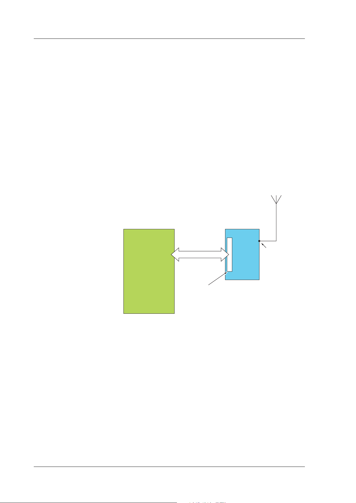
2.2 GM47 in a Communication System
Figure 2.1 illustrates the main blocks of a wireless communication
system using the GM47. It also shows the communication principles of
the system. The definitions in the figure, as used elsewhere in this
manual, are in accordance with the recommendations of GSM 07.07.
• The MS (mobile station) represents the GM47 module plus SIM
card. The module excluding SIM card, is known as the ME (mobile
equipment).
• The TE (terminal equipment) is a micro-controller (i.e., a computer)
and is a part of the application.
Wireless Communication System
Application
TE
(DTE)
ME status, responses
AT commands to control MS
GSM Network
MS
(GM47)
LZT 123 7263 R1C
Figure 2.1 Main Blocks in a Wireless System
15
Page 16
GM47/GM48 INTEGRATOR’S MANUAL
In accordance with the recommendations of ITU-T (International
Telecommunication Union - Telecommunications Standardisation
Sector) V.24, the TE communicates with the MS over a serial interface.
The functions of the GM47 follow the recommendations provided by
ETSI (European Telecommunications Standards Institute) and ITU-T.
ETSI specifies a set of AT commands for controlling the GSM element
of the module; these commands are supplemented by Sony Ericsson
specific commands.
To find out how to work with AT commands, see “Part 4: Using AT
Commands”, page 79.
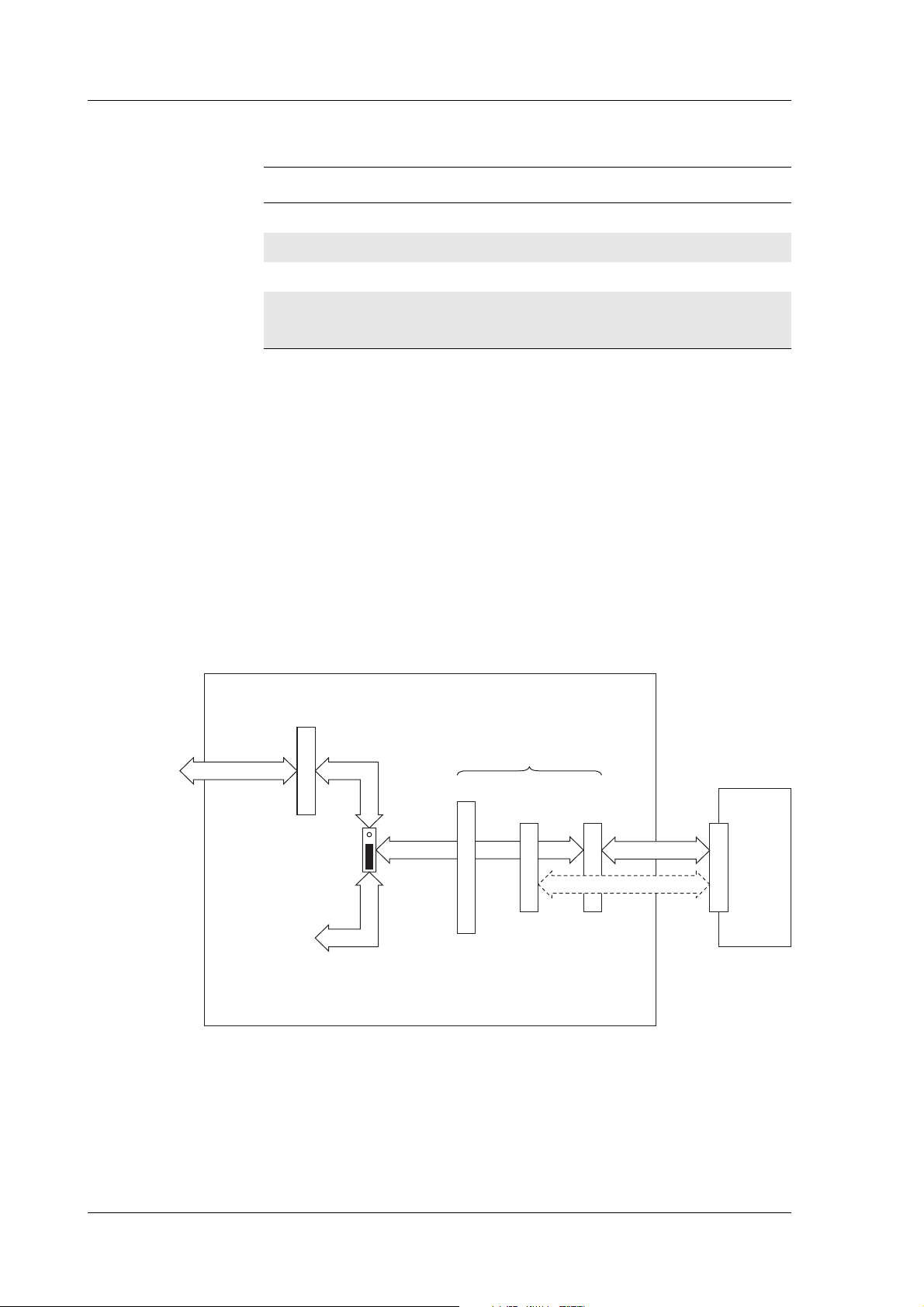
Figure 2.2 illustrates the interface between the module and the
application. The entire System Connector Interface is described in
detail in “System Connector Interface”, page 41
.
Signals
TE
(Application)
and power
60 pin
system connector
MS
(GM47)
Antenna
connector
Figure 2.2 The Interface between the Module and the Application
Note! ITU-T standards define TE and TA as DTE (Data Terminal Equipment)
and DCE (Data Circuit Terminating Equipment) respectively.
16
LZT 123 7263 R1C
Page 17

2.3 Features
The module performs a set of telecom services (TS) according to GSM
standard phase 2+, ETSI and ITU-T. The functions of the module are
implemented by issuing AT commands over a serial interface.
2.3.1 Types of Mobile Station
GM47 and GM48 are dual band mobile stations with the characteristics
shown in the tables below.
GM47 GSM900 E-GSM900 GSM1800
2. GM47/GM48 MODULES
Frequency Range (MHz) TX: 890-915
Channel spacing 200kHz 200kHz
Number of channels 173 carriers *8 (TDMA)
Modulation GMSK GMSK
TX phase accuracy < 5º RMS phase error (burst) < 5º RMS phase error (burst)
Duplex spacing 45MHz 95MHz
Receiver sensitivity at
antenna connector
Transmitter output power
at antenna connector
Automatic hand-over between GSM 900 and GSM1800
GM48 GSM850 GSM1900
Frequency Range (MHz) TX: 824-849
Channel spacing 200kHz 200kHz
RX: 935-960
GSM: channels 1 to 124
E-GSM: channels 975 to 1023
< –102dBm < –102dBm
Class 4
2W (33dBm)
RX: 869-894
TX: 880-890
RX: 925-935
TX: 1710-1785
RX: 1805-1880
374 carriers *8 (TDMA)
DCS: channels 512 to 885
Class 1
1W (30dBm)
TX: 1850-1910
RX: 1930-1990
Number of channels
Modulation GMSK GMSK
TX Phase Accuracy < 5º RMS phase error (burst) < 5º RMS phase error (burst)
Duplex spacing 45MHz 80MHz
Receiver sensitivity at
antenna connector
Transmitter output power
at antenna connector
Automatic hand-over between GSM850 and GSM1900
LZT 123 7263 R1C
123 carriers *8 (TDMA)
GSM: channels 128 to 251
< –102dBm < –102dBm
Class 5
0.8W (29dBm)
298 carriers *8 (TDMA)
PCS: channels 512 to 810
Class 1
1W (30dBm)
17
Page 18

2.3.2 Short Message Service
The module supports the following SMS services:
• Sending; MO (mobile-originated) with both PDU (protocol data
unit) and text mode supported.
• Receiving; MT (mobile-terminated) with both PDU and text mode
supported.
• CBM (cell broadcast message); a service in which a message is sent
to all subscribers located in one or more specific cells in the GSM
network (for example, traffic reports).
• SMS STATUS REPORT according to GSM 03.40.
• SMS COMMAND according to GSM 03.40.
The maximum length of an SMS message is 160 characters when using
7-bit encoding. For 8-bit data, the maximum length is 140 characters.
The module supports concatenated messages to extend this function. It
is disabled if CNMI 3,2 is set (See “AT+CNMI New Message
Indications to TE”, page 264).
GM47/GM48 INTEGRATOR’S MANUAL
2.3.3 Voice Calls
2.3.4 Data
The GM47 offers the capability of mobile originated and mobile
terminated voice calls, as well as supporting emergency calls.
Multi-party, call waiting and call deflection features are available.
Some of these features are network-operator specific.
For the inter-connection of audio, the module offers both single ended
and balanced analogue input and output lines. Direct interface to the
digital PCM (pulse code modulation) bus used within the module is
available, thus by-passing the internal analogue circuitry.
The module supports the following data protocols:
• GPRS (General Packet Radio Service)
Modules are Class B terminals, which provide simultaneous
activation and attachment of GPRS and GSM services. GM47
modules are GPRS 4+1 enabled devices, which are capable of
transmitting in one timeslot per frame (up link), and receiving at a
maximum of four timeslots per frame (down link).
• CSD (Circuit Switched Data)
GM47 modules are capable of establishing a CSD communication at
9.6kbps.
18
• HSCSD (High Speed Circuit Switched Data).
GM47 supports HSCSD communication, with one timeslot per
frame capacity in the up link and two timeslots per frame capacity in
the down link (2+1).
LZT 123 7263 R1C
Page 19

2. GM47/GM48 MODULES
2.3.5 SIM Card
An external SIM card with 3V or 5V technology, can be connected to
the module via its 60-pin system connector.
2.3.6 Average Power Consumption
Idle Mode Transmit/Operation
GSM850 and GSM900
GSM1800 and GSM1900
Note! The power consumption during transmission is measured at maximum
transmitted power.
2.3.7 Other Features
These include:
• 07.10 multiplexing.
• GPS interoperability.
• SIM application tool kit.
2.4 Service and Support
2.4.1 Web Pages
Voice/CSD <5mA <250mA (<2A peak)
Data (GPRS 4+1) <5mA <350mA (<2A peak)
Voice/CSD <5mA <250mA (<1.75A peak)
Data (GPRS 4+1) <5mA <350 mA (<1.75 A peak)
Visit our web site for the following information:
• where to buy modules or for recommendations concerning
• the telephone number for customer support in your region;
• FAQs (frequently asked questions).
The web site address is:
http://www.sonyericsson.com/M2M
2.4.2 Integrator’s Manual
This manual provides you with all of the information you need to
integrate the module into your application.
LZT 123 7263 R1C
accessories and components;
19
Page 20

2.4.3 Developer’s Kit
2.5 Precautions
GM47/GM48 INTEGRATOR’S MANUAL
Sony Ericsson provides the opportunity for designers to test the module
on a limited scale using its Developer’s Kit. The kit includes the
necessary accessories (software and hardware) required to build and test
an application. It includes the following:
• GSM module, GM47 or GM48;
• This integrator’s manual;
• Software developer’s kit and manual;
• Developer’s kit hardware.
All the user needs to provide, is a computer or micro-controller and the
expertise to use AT commands.
GM47 and GM48 modules are static sensitive devices (SSDs). Normal
SSD procedures for electronic devices should be used when handling
the modules. In “Part 3: Integrating the Module”, page 37 you will find
more information about safety and product care. Do not exceed the
environmental and electrical limits as specified in “Technical Data”,
page 75.
20
LZT 123 7263 R1C
Page 21

3. Abbreviations
Abbreviation Explanations
CBM Cell Broadcast Message
CBS Cell Broadcast Service
CSD Circuit Switched Data
DCE Data Circuit Terminating Equipment
DTE Data Terminal Equipment
DTMF Dual Tone Multi Frequency
EFR Enhanced Full Rate
EMC Electro-Magnetic Compatibility
ETSI European Telecommunication Standards Institute
3. ABBREVIATIONS
FR Full Rate
GPRS General Packet Radio Service
GPS Global Positioning System
GSM Global System for Mobile Communication
HR Half Rate
HSCSD High Speed Circuit Switched Data
ITU-T International Telecommunication Union - Telecommunications
ME Mobile Equipment
MO Mobile Originated
MS Mobile Station
MT Mobile Terminated
PCM Pulse Code Modulation
PDU Protocol Data Unit
RLP Radio Link Protocol
RF Radio Frequency
Standardisation Sector
LZT 123 7263 R1C
RTC Real Time Clock
SDP Service Discovery Protocol
SIM Subscriber Identity Module
SMS Short Message Service
21
Page 22

GM47/GM48 INTEGRATOR’S MANUAL
Abbreviation Explanations
TA Terminal Adapter
TE Terminal Equipment
THD Third Harmonic Distortion
TS Telecom Services
22
LZT 123 7263 R1C
Page 23

Part 2: Developer’s Kit
Product Photo/Illustration
Page 24

Page 25

1. Introduction
1.1 Overview
The developer’s kit is designed to get you started quickly. It contains all
the hardware you will need to begin the development of an application.
The only items you need to provide are; a computer or micro controller,
a SIM card and network subscription, and a knowledge of programming
with AT commands.
Note! Before connecting up and using the developer’s kit, we strongly
recommend you read “Part 3: Integrating the Module”, page 37 and all
of this section. There are many switches, jumpers and connector options
in the developer’s kit. A knowledge of the functionality of the GM47
module is therefore essential before you start altering the hardware
settings.
The main hardware in the developer’s kit is a screened box, containing
a board onto which you plug the GM47 module. Connectors, switches,
jumpers and SIM card holder are provided to allow you to configure and
access all the functions of the module.
1.2 Contents of the Kit
Please take the time to check the contents of your kit against the list
shown below. If any of the items are missing contact your supplier
immediately.
Developer’s kit - Part Number DPY 102 218
Contents:
Description Product Number Qty
Radio modem:
GM47 module or
GM48 module
GM47/GM48 developer’s kit (screened
box and development board)
Switched mode PSU 12V d.c. EPA-121DA-12 1
UK mains plug EN90POWERLEADUK 1
European mains plug EN90POWERLEADEU 1
DPY 102 201
1
DPY 102 204
KRY 101 1907 1
LZT 123 7263 R1C
25
Page 26
GM47/GM48 INTEGRATOR’S MANUAL
Description Product Number Qty
Cable with connector/cable serial 9-9 PIN DB9(M)-DB9(F) 1
Portable handsfree 2002-1-24 1
Quad band antenna RG174 1
Data carrier/CD-ROM containing:
Software Manual;
Integrator’s Manual
1.3 General Functioning of the Kit
The following block diagrams are provided to help you understand the
general principles of operation of the developer’s kit.
You have the following options as shown in Figure 1.1:
• Connect the GM47 internally, direct to J4 or position it externally
and connect to J10 via a flat cable.
• Use the kit’s connectors to access and control the GM47 (all
switches and jumpers in their default positions).
• Access and control the GM47 directly via J12 and a flat cable. This
allows you to selectively bypass any circuits contained on the board,
and test your own application.
Pin header
J12
60 pins male
1.27mm pitch
External
Application
LZY 213 1319 1
Pins connected in parallel
J11
J4J10
26
User selectable
jumpers
Developer's
board circuits
and ports
Developer's board
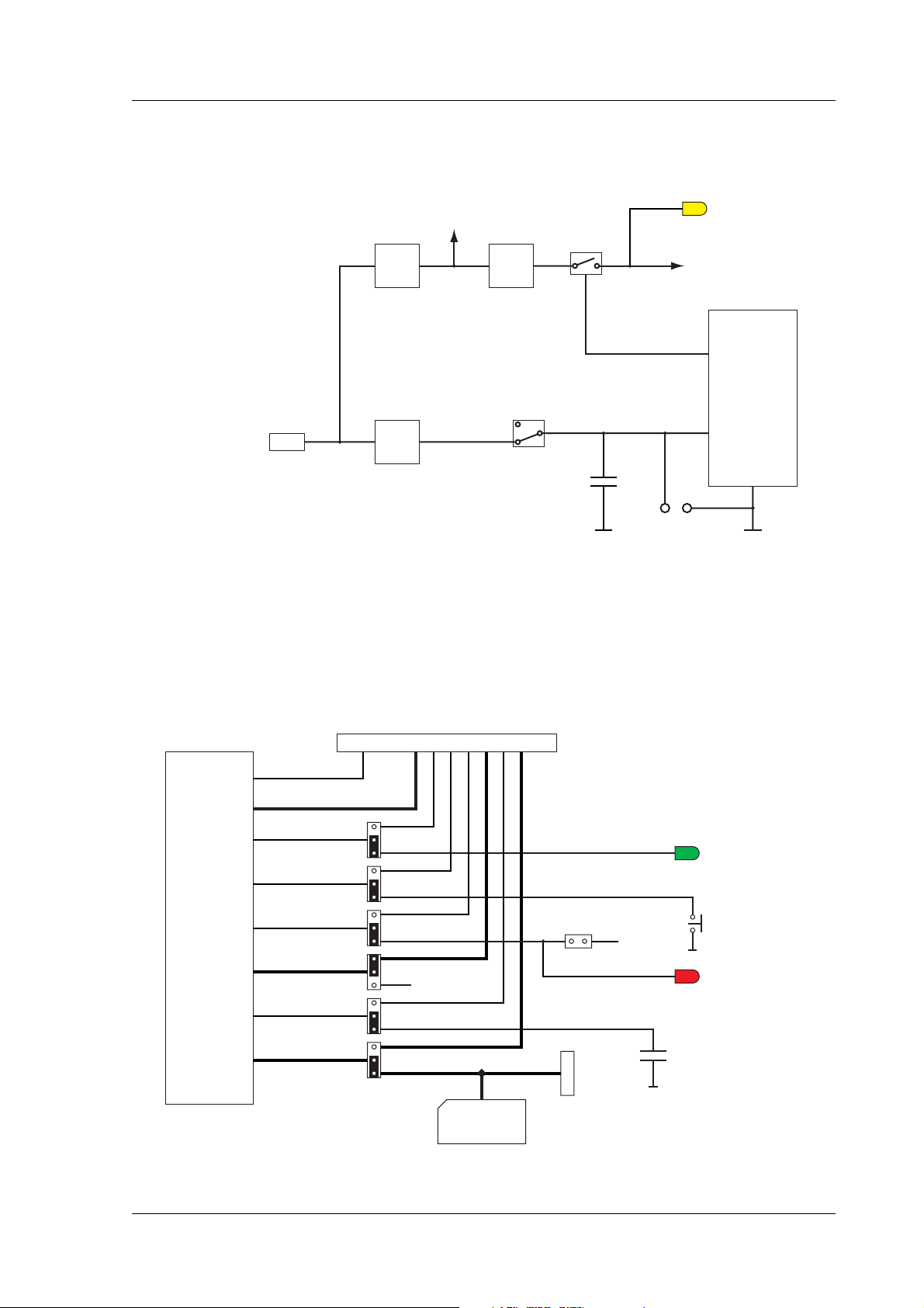
Figure 1.2 shows the various on-board voltages and how they are fed to
the GM47 and other circuitry. The developer’s board is powered by an
external power supply connected to Vcc.
fit direct to J4
alternate flat cable to J10
Pin headers
Pin header
60 pins male
2.54mm pitch
60 pins female
1.27mm pitch
Figure 1.1 Module connections to the developer’s board
LZT 123 7263 R1C
GM47
Page 27
1. INTRODUCTION
12v
DC Power Socket,
Input 10..15V
5V to development
board circuits
Switched
when VIO
VIO present
LED
present
5V
reg.
2V7
reg.
2V7
To development
board & interface
circuits
VIO
GM47
3V8
VCC
3V8
reg.
Vcc
+-
TP4 TP5
Figure 1.2 Power supply connection and the on-board voltages
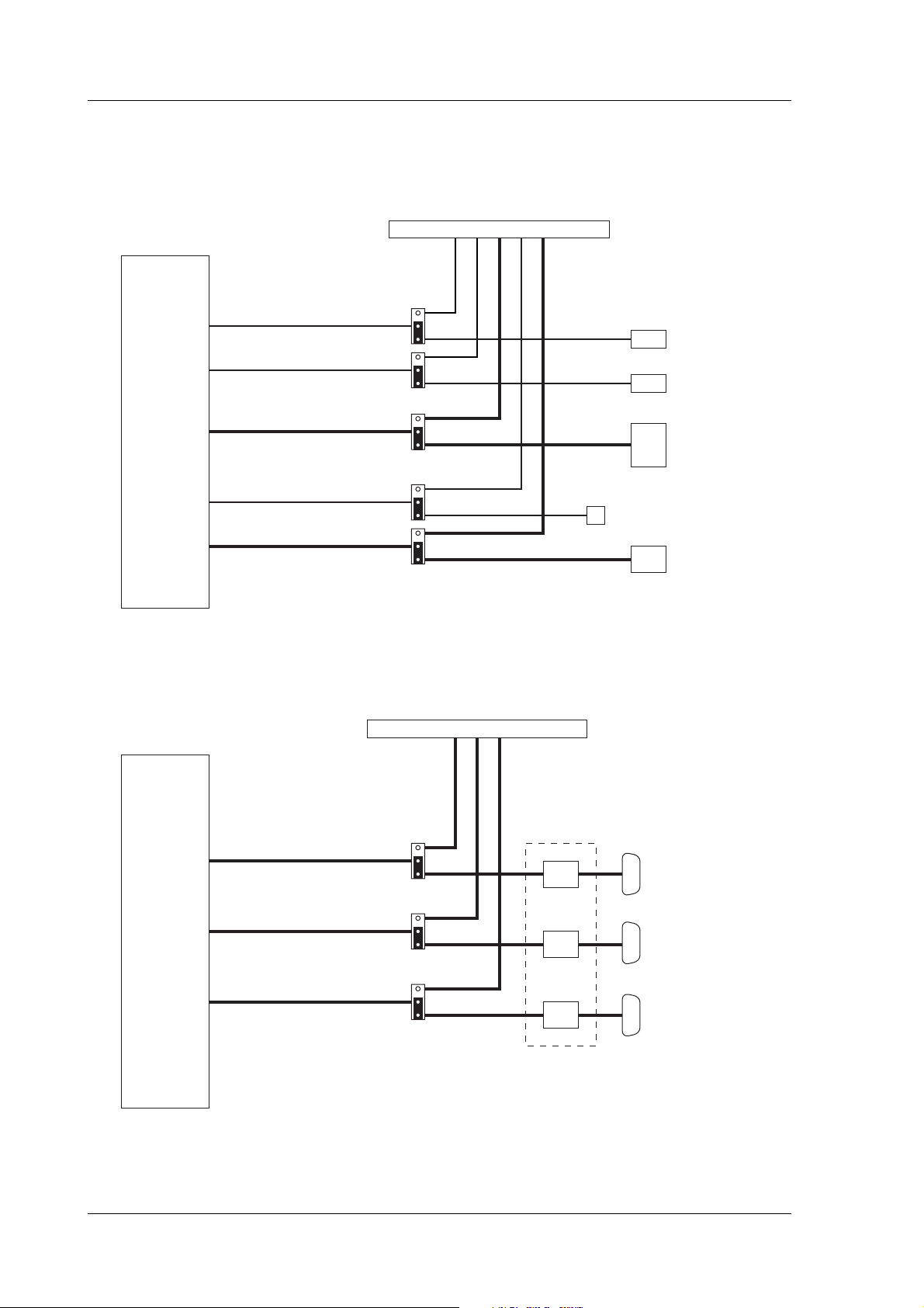
Figure 1.3, Figure 1.4 and Figure 1.5 show how various signals are
routed on the developer’s board. Thicker lines indicate multiple signals.
GM47
VIO
General purpose I/O
LED
ON/OFF
SERVICE
I²C
VRTC
SIM
Selectable
Jumpers
n/c
J12
U10 SIM
SW4
2V7
J5
SIM holder with
SIM presence
switch (to DGND)
STATUS L ED
(Blinks when
connected to network)
ON/OFF
SERVICE LED
(Lit when SW4 closed)
0.22F
LZT 123 7263 R1C
Figure 1.3 Miscellaneous signals, connection and routing
27
Page 28
GM47
GM47/GM48 INTEGRATOR’S MANUAL
ATM S
AFMS
MICN, MICP, BEARN, BEARP
Buzzer
PCM
Selectable
Jumpers
J12
3.5mm socket
3.5mm socket
RJ11 connector
Buzzer
8 pin Mini-DIN
(Audio out)
EAR
(Audio in)
MIC
Handset
PCM
GM47
TD, RD, DTR, DCD,
RTS, CTS, RI
TD2, RD2 & SERVICE
TD3 & RD3
Figure 1.4 Audio signals, connection and routing
J12
UART1 (EDB)
UART2 (ACB)
UART3
Selectable
jumpers
Level shifters
28
Figure 1.5 Comms signals, connection and routing
LZT 123 7263 R1C
Page 29
2. USING THE DEVELOPER’S KIT
2. Using the Developer’s Kit
This section provides you with the information needed to setup and use
the developer’s kit. Before changing switch and jumper settings, refer
to “2.3 Jumpers, Switches and Connectors”, page 32.
Front and rear views of the developer’s kit are shown below. To access
the inside, remove the 8 screws on the top of the box and the cover plate.
v
12
UART3
RF
Vcc
IO
C
N
OFF
ON
D
V
5
+
C
OFF
APP
ON/OFF
Figure 2.1 Front view
UART1
GM47/GM
VIO
AN
H
CE
S
I
V
R
ATU
SE
ST
48 Developer's Kit
SET
D
M
PC
MIC
UART2
EAR
LZT 123 7263 R1C
Figure 2.2 Rear view
29
Page 30

2.1 Start up Check List
To use the developer’s kit in standard format check the following:
• With the case lid removed, make sure the GM47 module is plugged
into J4 and the RF lead is connected to the rear of the module;
• Add your SIM card;
• Check the jumpers are in their default positions. Refer to Figure 2.3;
• Connect the serial cable between your computer and UART1 on the
rear panel;
• Connect the antenna to the RF connector on the rear panel;
• Connect the audio equipment if required;
• Plug the external power supply into the socket marked 12v on the
front panel;
• Switch Vcc to ON;
• Push ON/OFF for at least 2 seconds until the yellow VIO LED is on.
GM47/GM48 INTEGRATOR’S MANUAL
Your developer’s kit should now be operational and ready to receive AT
commands.
30
LZT 123 7263 R1C
Page 31

2. USING THE DEVELOPER’S KIT
2.2 Developer’s Board Overlay
Figure 2.3 shows the developer’s board, including the position of all the
connectors, switches and jumpers (default positions). You will notice
that many jumpers are labelled “SW”. This is because the board was
previously fitted with DIL switches.
UART2
(ACB)
JP21
JP18
Ground stud
J12
Application Connector
59 1
260
UART1
(EDB)
SW8
SW11
SW7
U10
SIM
Holder
SW1
SW9
SW6
SW3
J11
159
Test Connector
RF connector
SIM test
J5
connector
2
17
J10
2
System Connector (for flat cable)
60 2
60
59 1
TP5 TP4
J4
159
System Connector
UART3
VCC
12v
DC Power
10..15V d.c.
LZT 123 7263 R1C
Socket,
Input
NC/OFF/ON
power to
Vcc
module
JP24
SW4
DCIO
Maintain in
OFF position
(Not used with this module.
Only present for backward
compatibility)
SW10
ON/OFF
(module)
SW5
VIO
STATUS
60
Handset PCM MIC
SERVICE
Figure 2.3 Developer’s board overlay
Audio in
(ATMS)
EAR
Audio out
(AFMS)
31
Page 32

GM47/GM48 INTEGRATOR’S MANUAL
2.3 Jumpers, Switches and Connectors
You will notice that many jumpers are labelled “SW”. This is because
the board was previously fitted with DIL switches. All jumpers are
located on the developer’s board (see “Developer’s board overlay”,
page 31).
Jumper Signal Setting
JP18 TD Maintain jumper in
JP21 JP18
lower default position
JP21 RD Maintain jumper in
lower default position
JP24 Reserved for
future use
MUST remain open to prevent
damage to the module. As an extra
precaution, maintain DCIO in the OFF
position
SW4 SERVICE Connect the pins using the floating
connector ONLY when programming
the module or logging data
SW1, SW3, SW5,
SW6, SW7, SW8,
SW9, SW10,
SW11, J11 links
See diagram
below
Default positions shown below. Move
any “SW” jumper to the right-hand
position to divert the signal to
connector J12. Remove the J11 links
to bypass J8, J9 or CP1 and process
audio signals externally
J11
SIMRST
SIMCLK
SCL
SDA
SW8 SW1
VRTC
RD3 (RX3)
TD3 (TX3)
SW11 SW6
PCMULD
PCMIN
PCMOUT
PCMCLK
SW7 SW3
BEARP
SERVICE
AFMS
ATMS
SW10 SW5
SW9
ON/OFF
PRESENCE
SIMVCC
SIMDAT
BUZZER
LED
RI
DCD
DTR
CTS
RTS
RD (DFMS)
TD (DTMS)
RD2 (CFMS)
TD2 (CTMS)
PCMDLD
PCMSYN
MICN
MICP
BEARN
4847
49
59 60
50
The links shown
on J11 must be
in place to
access audio
on J8, J9 or CP1
32
LZT 123 7263 R1C
Page 33

2. USING THE DEVELOPER’S KIT
All switches are mounted on the front panel of the developer’s box.
Switch Description Operation
Vcc Toggle switch Switches power from external power supply to
module. Has three positions; NC, OFF and ON.
Switch to ON to connect power to the module
ON/OFF Push button
switch
Switches module on and off. To power up the
module, push button for at least 2 seconds,
until the yellow VIO LED is on. Repeat the
process to turn the module off
DCIO Toggle switch Maintain in OFF position. Included only for
backwards compatibility
Connector Description Connections
UART1
(EDB)
9-way
Dsocket
(accessible
on the rear
Full 9-pin RS232 communication port. Used
during run-time to communicate with the
module (AT-commands, data transmission,
etc.)
panel)
DCD
RD
RTS
TD
CTS
DTR
1
6
2
7
3
8
4
9RI
5
UART2
(ACB)
9-way
Dsocket
(accessible
on the rear
panel)
UART3 9-way
Dsocket
(accessible
on the rear
panel)
3 line RS232 communications port
(+SERVICE). Used during service and
maintenance operations. Also used to
download new software to the module
1
6
RD2
SERVICE
TD2
2
7
3
8
4
9
5
3 line serial port. RS232 levels
1
6
RD3
TD3
2
7
3
8
4
9
5
LZT 123 7263 R1C
33
Page 34

GM47/GM48 INTEGRATOR’S MANUAL
Connector Description Connections
Handset RJ11 socket Connector for a standard telephone
handset. As PCM paths are open inside the
module, a default short circuit is made
between PCMDLD-PCMIN and PCMULDPCMOUT signals on test connector J11 to
enable analogue audio in downlink and
uplink directions. Jumpers are in place
between pins 48 & 50 and between pins 47
& 49
Pin # Signal
1234
1MICN
2BEARN
3BEARP
4MICP
PCM 8 pin mini-DIN
connector
Carries PCM signals
Pin # Signal
1 VIO (2.75V d.c. output)
2PCMULD
3PCMDLD
J4 SYSTEM
connector
4 PCMCLK
5PCMSYNC
6DGND
7PCMIN
8PCMOUT
9DGND
Allows direct connection of the module to
the development board (see Figure 2.3,
1
2
34
page 31)
9
8
6
5
7
J5 SIM card test
connector
Connector to gain access to the SIM card
signals, which are connected in parallel with
U10
Pin # Signal
1SIMVCC
2SIMRST
3SIMCLK
4SIMDAT
5 SIMPRESENCE
6SIMGND
7SIMGND
U10 SIM Holder Connector for SIM card. Signals are also
present at test connector J5, described
above
EAR 3.5 mm 2-pole
jack socket
Audio output (unbalanced) or Audio From
Mobile Station (AFMS). Make sure jumpers
are in place between pins 48 & 50 and
between pins 47 & 49
ground signal
MIC 3.5mm 2-pole
jack socket
Audio input (unbalanced) or Audio To
Mobile Station (ATMS). Signal source must
be AC-coupled as a bias voltage for
electret microphones is provided
(2.0 - 2.5V d.c.). Make sure Jumpers are in
place between pins 48 & 50 and between
pins 47 & 49
34
LZT 123 7263 R1C
Page 35

2. USING THE DEVELOPER’S KIT
Connector Description Connections
J10 SYSTEM
connector
J11 TEST
connector
J12 Application
connector
12v 2.1mm DC
Power Socket
RF SMA panel
socket
For optional flat cable connection between
the module and the development board
(see Figure 2.3, page 31)
60 pin, 2.54mm pitch, dual row pin header
that carries all signals present at the system
connector of the module. Used for easy
testing of the signals (see Figure 2.4,
page 36)
For flat cable connection between a host
application and the module. Most of the
signals pass through jumpers that allow the
developer to select whether a specific
signal is routed to/from the development
board or to/from the host application. If no
application is connected to J12, these
jumpers (SW1, SW3, SW5, SW6, SW7, SW8,
SW9, SW10 & SW11) serve as on/off switches
for the module signals (see Figure 2.3,
page 31)
Allows connection of an
external power supply.
Between 10V and 15V d.c. at
6 watts is required
Connect the supplied antenna
LZT 123 7263 R1C
35
Page 36

GM47/GM48 INTEGRATOR’S MANUAL
2.4 System Connector Pin Assignments
Refer to the table below when monitoring signals on, or connecting to,
J10, J11 or J12. The table shows the system-connector pin assignments
for the GM47 module.
1 VCC DGND 2
3 VCC DGND 4
5 VCC DGND 6
J10, J11 & J12 pin
numbering
viewed from the
front of the
developer’s box
12
59 60
7 VCC DGND 8
9 VCC DGND 10
11 VCC DGND 12
13 Reserved for future use ON/OFF 14
15 SIMVCC SIMPRESENCE 16
17 SIMRST SIMDAT 18
19 SIMCLK DAC 20
21 IO1 IO2 22
23 IO3 IO4 24
25 VRTC ADC1 26
27 ADC2 ADC3 28
29 SDA SCL 30
31 BUZZER OUT5 32
33 LED VIO 34
35 TX_ON RI 36
37 DTR DCD 38
39 RTS CTS 40
41 TD (DTMS) RD (DFMS) 42
43 TD3 (TX3) RD3 (RX3) 44
45 TD2 (CTMS) RD2 (CFMS) 46
47 PCMULD PCMDLD 48
49 PCMOUT PCMIN 50
51 PCMSYNC PCMCLK 52
53 MICP MICN 54
55 BEARP BEARN 56
57 AFMS SERVICE 58
59 ATMS AGND 60
36
Figure 2.4 System connector pin assignments
LZT 123 7263 R1C
Page 37

Part 3: Integrating the Module
Product Photo/Illustration
Page 38

Page 39

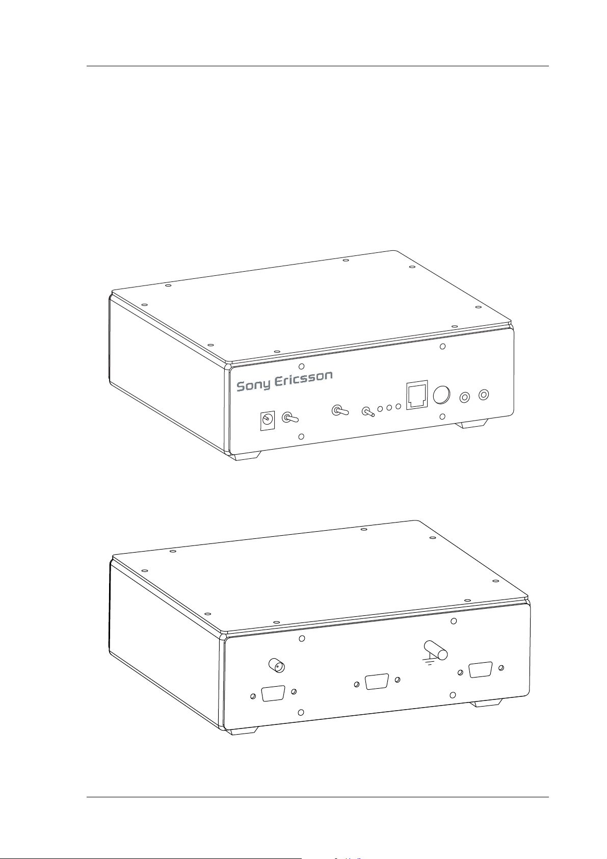
1. Mechanical Description
1.1 Interface Description
The pictures below show the mechanical design of the GM47 along
with the positions of the different connectors and mounting holes. The
GM47 is protected with AISI 304 stainless steel covers that meet the
environmental and EMC requirements.
Mounting hole/ground connection
Antenna connector
System connector
LZT 123 7263 R1C
Figure 1.1 GM47 viewed from below
Figure 1.2 GM47, viewed from above
Please note the following:
• Mounting holes positioned at the corners make it possible to
securely bolt the module into your application.
39
Page 40

GM47/GM48 INTEGRATOR’S MANUAL
• Keypad, display, microphone, speaker and battery are not part of the
module.
• The SIM card is mounted in your application, external to the
module.
• The System Connector is a 60-pin, standard 0.05 in (1.27mm) pitch
type. The pins and their electrical characteristics are described in
“2. System Connector Interface”, page 41.
• Information about the Antenna Connector is found in
“3. Antenna Connector”, page 68.
1.2 Physical Dimensions
2.20 (4x)
33.00
50.00
46.40
4.78
9.00
1.80
2.86
2.053.80
30.20
2.30
3.00
7.15 2.90
4.60
2.80
40
Figure 1.3 Dimensions of the GM47
Measurements are given in millimetres. See also “Technical Data”,
page 75.
LZT 123 7263 R1C
Page 41

2. System Connector Interface
2.1 Overview
Electrical connections to the module (except the antenna), are made
through the System Connector Interface. The system connector is a
60-pin, standard 0.05in (1.27mm) pitch device.
The system connector allows both board-to-board and board-to-cable
connections to be made. Use a board-board connector to connect the
module directly to a PCB, and a board-cable connector to connect the
module via a cable.
Figure 2.1 below shows the numbering of the connector pins.
A ground connection is provided at the mounting hole next to the RF
connector on the module as shown below. Connect this ground point to
the DGND pins of the module by the shortest, low-impedance path
possible. The purpose of this connection is to allow any ESD picked up
by the antenna to bypass the module’s internal ground path.
Ground
connection
Pin 59 Pin 1
Pin 60 Pin 2
Figure 2.1 GM47, viewed from underneath
LZT 123 7263 R1C
41
Page 42

GM47/GM48 INTEGRATOR’S MANUAL
The following table gives the pin assignments for the system connector
interface and a short description for each signal.
Note! Under the heading “Dir” in the table, module input and output signals
are indicated by the letters I and O respectively.
Pin Signal Name Dir Signal Type Description
1 VCC - Supply Power supply
2 DGND - - Digital ground
3 VCC - Supply Power supply
4 DGND - - Digital ground
5 VCC - Supply Power supply
6 DGND - - Digital ground
7 VCC - Supply Power supply
8 DGND - - Digital ground
9 VCC - Supply Power supply
10 DGND - - Digital ground
11 VCC - Supply Power supply
12 DGND - - Digital ground
13 Reserved for
14 ON/OFF I Internal pull
15 SIMVCC - Digital 3 V/5V SIM card power supply. Power output
16 SIMPRESENCE I Internal pull
17 SIMRST O Digital 3V/5V SIM card reset
18 SIMDATA I/O Digital 3V/5V SIM card data
19 SIMCLK O Digital 3V/5V SIM card clock
20 DAC O Analogue Digital to analogue converter
21 IO1 I/O Digital 2.75 General purpose input/output 1
future use
up, open drain
up, open drain
Turns the module on and off.
Former WAKE_B
from module for SIM Card
SIM Presence
A “1” indicates that the SIM is missing; a
“0” that it is inserted
42
22 IO2 I/O Digital 2.75 General purpose input/output 2
23 IO3 I/O Digital 2.75 General purpose input/output 3
24 IO4 I/O Digital 2.75 General purpose input/output 4
25 VRTC I Supply 1.8V Supply for real time clock
26 ADC1 I Analogue Analogue to digital converter 1
27 ADC2 I Analogue Analogue to digital converter 2
LZT 123 7263 R1C
Page 43

2. SYSTEM CONNECTOR INTERFACE
Pin Signal Name Dir Signal Type Description
28 ADC3 I Analogue Analogue to digital converter 3
29 SDA I/O 2.75, internal
pull up
30 SCL O 2.75, internal
pull up
I2C data
I2C clock
31 BUZZER O Digital 2.75 Buzzer output from module
32 OUT5 O Digital 2.75 Programmable output 5
33 LED O Digital 2.75 Flashing LED
34 VIO O Power Out
2.75V
Module power indication. VIO is a
2.75V at 75mA output supply that can
be used to power external circuitry that
interfaces to the GM47
35 TX_ON O Digital 2.75 This output indicates when the GSM
module is going to transmit the burst
36 RI O Digital 2.75 Ring Indicator (UART1)
37 DTR I Digital 2.75 Data Terminal Ready (UART1)
38 DCD O Digital 2.75 Data Carrier Detect (UART1)
39 RTS I Digital 2.75 Request To Send (UART1)
40 CTS O Digital 2.75 Clear To Send (UART1)
41 TD I Digital 2.75 Transmitted Data (UART1).
Data from DTE (host) to DCE (module).
Former DTMS
42 RD O Digital 2.75 Received Data (UART1).
Data from DCE (module) to DTE (host).
Formerly DFMS
43 TD3 I Digital 2.75 UART3 transmission
44 RD3 O Digital 2.75 UART3 reception
45 TD2 I Digital 2.75 UART2 transmission. Used for flashing
the memory. Former CTMS
46 RD2 O Digital 2.75 UART2 Reception. Used for flashing the
memory. Former CFMS
47 PCMULD I Digital 2.75 DSP PCM digital audio input
48 PCMDLD O Digital 2.75 DSP PCM digital audio output
49 PCMOUT O Digital 2.75 Codec PCM digital audio output
50 PCMIN I Digital 2.75 Codec PCM digital audio input
51 PCMSYNC O Digital 2.75 DSP PCM frame sync
52 PCMCLK O Digital 2.75 DSP PCM clock output
53 MICP I Analogue Microphone Input positive
54 MICN I Analogue Microphone Input negative
55 BEARP O Analogue Speaker output positive
LZT 123 7263 R1C
43
Page 44

GM47/GM48 INTEGRATOR’S MANUAL
Pin Signal Name Dir Signal Type Description
56 BEARN O Analogue Speaker output negative
57 AFMS O Analogue Audio output from module
58 SERVICE I 2.7V Flash programming voltage for the MS.
59 ATMS I Analogue Audio input to module
60 AGND - - Analogue ground
Enable logger information if not
flashing. Formerly VPPFLASH
2.2 General Electrical and Logical Characteristics
Many of the signals, as indicated in the table above, are high-speed
CMOS logic inputs or outputs powered from a 2.75V±5% internal
voltage regulator, and are defined as Digital 2.75V. Whenever a signal
is defined as Digital 2.75V, the following electrical characteristics
apply.
Parameter Min. Max. Units
High Level Output Voltage (VOH), Io= –2mA 2.2 2.75 V
Low Level Output Voltage (VOL), Io = 2mA 0 0.6 V
High Level Input Voltage (VIH) 1.93 2.75 V
Low Level Input voltage (VIL) 0 0.8 V
Note! Unused pins can be left floating.
2.2.1 General Protection Requirements
• All 2.75 V digital inputs will continuously withstand and suffer no
damage in the power-on or power-off condition when subjected to
any voltage from -0.5V to 3.47V (3.3V+5%).
• All 2.75V digital outputs will continuously withstand a short circuit
to any other voltage within the range 0V to 3V.
• All analogue outputs will continuously withstand a short circuit to
any voltage within the range 0V to 3V.
• The SIM output signals and the SIMVCC supply will continuously
withstand a short circuit to any voltage within the range 0V to 5.8V.
44
LZT 123 7263 R1C
Page 45

2. SYSTEM CONNECTOR INTERFACE
2.3 Grounds
Pin Signal Description
2, 4, 6, 8, 10, 12 DGND Digital ground
60 AGND Analogue ground
There are two ground connections in the GM47, AGND (analogue
ground) and DGND (digital ground). Pin assignments are shown in the
table above.
Note! AGND and DGND are connected at a star point inside the module. They
must not be joined together in your application.
2.3.1 Analogue Ground - AGND
AGND is the return signal, or analogue audio reference, for ATMS
(Audio To Mobile Station) and AFMS (Audio From Mobile Station).
Parameter Limit
I
max
2.3.2 Digital Ground - DGND
DGND is the reference or return signal for all system interface digital
signals and is also the d.c. return for SERVICE and the power supply,
VCC. Connect all DGND pins together in your application in order to
carry the current drawn by the module.
2.4 VCC - Regulated Power Supply Input
Pins Signal Description
1, 3, 5, 7, 9, 11 VCC regulated power supply input
Power is supplied to the module VCC pins, from an external source.
Connect all VCC pins together in your application in order to carry the
current drawn by the module.
≅12.5mA
LZT 123 7263 R1C
45
Page 46

GM47/GM48 INTEGRATOR’S MANUAL
The electrical characteristics for VCC are shown in the table below.
Parameter Mode Limit
Nominal 3.6V
Vcc supply voltage
Maximum allowable voltage
drop
Current drawn, at full TX
power
a. Measured at system connector pins.
Note! GM47 has no internal capacitance to supply the large current peaks
during GSM burst transmission. We recommend you follow these
general guidelines:
• Fit a low ESR electrolytic capacitor close to the module:
> 1,000µF;
<100mΩ ESR.
• Make sure power supply to module line resistance is < 200 mΩ.
2.5 ON/OFF and External Power Signal
Tolerance
including ripple
Over-voltage limit 5.5 V
Maximum ripple TBD
Burst transmission 200 mV
3.4V - 4.0V
a
<350mA (average)
<2A (peak)
Pin Signal Dir Description
14 ON/OFF I Pulse signal to turn the module on or off
34 VIO O 2.75 V supplied by the module
2.5.1 Switching the module ON and OFF
The module is turned on and off by momentarily grounding the
ON/OFF pin. This input should be driven by an open collector, or other
device which will not tie the input high, to allow the internal alarm clock
function to operate. See the table below for exact characteristics. In the
OFF state the current consumption of the module is less than 100µA.
The ON/OFF signal is a digital input with the following characteristics:
Parameter Min. Typ. Max. Units
Voltage HIGH level (FALSE) VCC V
Voltage LOW level (TRUE) 0 0.3 x VCC V
Pull-up resistance (internal) 39 kΩ
46
LZT 123 7263 R1C
Page 47

2. SYSTEM CONNECTOR INTERFACE
The following timing diagram illustrates both power-up and powerdown processes.
Module on Module off
ON/OFF
VIO
Module
powered
t
1
t
pwr
Module power-up Module power-down
t
2
Figure 2.2 ON/OFF timing and VIO performance
Times are defined as follows:
Time Description Min. Typ. Max. Units
t
1
t
2
Turn-on pulse time ≥2 s
Turn-off pulse time ≥ 1 s
Hardware-reset pulse time
a
>10 s
2.5.2 VIO - 2.75V Supply
VIO provides an output voltage derived from an internal 2.75V
regulator. Its electrical characteristics are shown below.
You can use this output for the following:
• to indicate that the module is alive;
• to power interface circuits, external to the module.
t
pwr
Time for VIO and internal voltages
to be established
100 200 ms
a. Active only when a full system reset is required.
Parameter Min. Typ. Max. Units
Output Voltage (I
Load current 75 mA
= 50mA) 2.70 2.75 2.85 V
load
LZT 123 7263 R1C
47
Page 48

2.6 Analogue Audio
Pin Signal Dir Description
57 AFMS O Audio from mobile station
59 ATMS I Audio to mobile station
60 AGND - Ground (return) for analogue audio
ATMS is the audio input, and AFMS is the audio output, of the module.
These signals can be used in Hands-free or Portable Hands-free mode.
Hands-free Mode
This mode is used for audio accessories, such as car kits and hands-free
equipment.
Portable Hands-free Mode
GM47/GM48 INTEGRATOR’S MANUAL
This is the default mode. It activates a different amplification factor in
the ME, and activates a 2V microphone bias level for ATMS. The bias
level is adjustable using AT*E2EAMS.
2.6.1 Audio To Mobile Station - ATMS
ATMS is the analogue audio input to the module. Internally, the signal
is sent to the CODEC (COder/DECoder), where it is converted to digital
audio in PCM (Pulse Code Modulation) format. The encoded audio is
sent to PCMOUT via the internal PCM bus.
ATMS provides a DC bias when it is used as the microphone input in
Portable Hands-free applications. All other sources must be
a.c.-coupled to avoid attenuation of low frequencies, and to prevent
incorrect biasing or damage to the ATMS input. Use a capacitor greater
than the value shown in the table below.
The ATMS input is a passive network followed by the transmit part of
the CODEC.
Parameter Limit
Application driving impedance (0.3 - 3.5kHz) ≤ 300Ω
48
AC coupling capacitance
Module input impedance (0.3 - 3.5kHz) >50kΩ
Low frequency cut-off (-3 dB) 300Hz ± 50Hz
a
≥ 1µF
LZT 123 7263 R1C
Page 49

2. SYSTEM CONNECTOR INTERFACE
Parameter Limit
High frequency cut-off (–3 dB) > 3500Hz ± 50Hz
Output d.c. bias level
Additional Gain in Portable hands-free mode 28.5 dB
Hands-free mode 0V
Portable hands-free mode 2.0 V ± 0.1V
a. The a.c.-coupling capacitance must be supplied by your application, unless
a d.c.-coupled microphone is used.
The following tables show the nominal PGA (programming gain
settings). For more information see the relevant AT commands.
Maximum input voltage limit: 245mV
Input Input (mV
ATMS 245 0 13 3
) TXAGC (dB) AUX AMP
rms
Maximum input level at MICI, 61.4mV
rms
gain
rms
PCMOUT (dBm0)
output at
PCMOUT = 3dBm0
Input Differential
input (mV
rms
TXAGC (dB) AUX AMP
)
PCMOUT (dBm0)
gain
MICN
MICP
61.4 0 25 3
Output at AFMS for 3dBm0 at PCMIN
Input dBm0 RXPGA Volume
PCMIN 3 0 0 436
Output at BEARN/BEARP for 3dBm0 at PCMIN
Input dBm0 RXPGA Volume
PCMIN 3 0 0 388
2.6.2 Audio From Mobile Station - AFMS
AFMS is the analogue audio output from the module and may be used
to drive a speaker or the ear-piece in a portable hands-free accessory.
PCM digital audio signals, entering the module through the PCMIN pin,
are translated to analogue signals by the CODEC. See “2.7 PCM Digital
Audio”, page 52 for further information.
control (dB)
control (dB)
AFMS (mV
BEAR (mV
rms
rms
)
)
LZT 123 7263 R1C
49
Page 50

GM47/GM48 INTEGRATOR’S MANUAL
The table below shows the audio signal levels for AFMS.
Parameter Limit
Speaker impedance 64Ω to 1kΩ
Output Capacitance 2.2µF ±10%
Levels (THD <5 %)
2.6.3 Microphone Signals
Pin Speaker signals Dir Function
53 MICP I Microphone positive input
54 MICN I Microphone negative input
MICP and MICN are balanced differential microphone input pins.
These inputs are compatible with an electret microphone. The
microphone contains an FET buffer with an open drain output, which is
supplied with at least +2V relative to ground by the module as shown
below.
Drive capability into 5kΩ
(0.3 - 3.5kHz)
Drive capability into 1.5kΩ
(0.3 - 3.5kHz)
Drive capability into 150 Ω
(at 1kHz)
2 - 2.5V
@ 1mA
1k
68nF
MICP
>2.4V
>2.2V
>1.3V
p-p
p-p
p-p
50
CODEC
GM47
68nF
MICN
1k
AGND
Figure 2.3 Microphone connections to the module
LZT 123 7263 R1C
Page 51

2.6.4 Speaker Signals
2. SYSTEM CONNECTOR INTERFACE
Pin Speaker signals Dir Function
55 BEARP O Speaker positive output
56 BEARN O Speaker negative output
BEARP and BEARN are the speaker output pins. These are
differential-mode outputs. The electrical characteristics are given in the
table below.
Parameter Limit
Output level (differential) ≥4.0V
Output level (dynamic load = 32Ω) ≥2.8V
Gain PCMINa to BEARP/BEARN (differential)
Distortion at 1 kHz and maximum output level ≤ 5%
Offset, BEARP to BEARN ±30mV
Ear-piece mute-switch attenuation ≥ 40dB
–9dB ± 1
a. See PCMIN signal in “2.7 PCM Digital Audio”, page 52
The following table shows the ear piece impedances that can be
connected to BEARP and BEARN.
Ear piece model Impedance Tolerance
Dynamic ear piece [32Ω + 800µH] // 100pF ±20%
Dynamic ear piece [150Ω + 800µH] // 100pF ±20%
Piezo ear piece 1kΩ + 60nF ±20%
pp
pp
LZT 123 7263 R1C
51
Page 52

2.7 PCM Digital Audio
Pin Signal Dir Function
52 PCMCLK O PCM clock
51 PCMSYNC O PCM frame sync
47 PCMULD I PCM audio input to DSP
48 PCMDLD O PCM audio output from DSP
50 PCMIN I PCM audio input to Codec
49 PCMOUT O PCM audio output to Codec
Figure 2.4 shows the PCM (Pulse Code Modulation) digital audio
connection for external devices. These connections can be used to
process PCM digital audio signals, bypassing the module’s internal
analogue audio CODEC.
GM47/GM48 INTEGRATOR’S MANUAL
GM47
PCMSYNC & PCMCLK
DSP
Link for internal
digital-audio processing
PCMDLD
PCMULD
System connector
PCMIN
PCMOUT
CODEC
Analogue
audio
signals
Figure 2.4 Pin connections to digital audio
Note! When no external audio processing is performed, the following pins
must be connected together:
• PCMDLD to PCMIN
52
• PCMULD to PCMOUT
Electrical characteristics
Digital 2.75V CMOS input/output electrical characteristics apply.
LZT 123 7263 R1C
Page 53

2.7.1 PCM Data Format
13-Bit PCM Mode
2. SYSTEM CONNECTOR INTERFACE
All of the module’s PCM signals, including signals between its CODEC
and DSP conform to the PCM data I/O format of the industry standard
DSP from Texas Instruments.
PCMCLK (bit clock) and PCMSYNC (frame syncronisation) are both
generated by the DSP within the module.
The DSP within the module is the master therefore all external PCM
clocks and data from external devices must be synchronized to it
Bit Contents
D15 to D14 Equal to D13
D13 to D1 Two's complement of the 13-bit PCM
D0 LSB, not used
The module implements 13-bit PCM with the 13-bit data embedded in
a 16-bit word within a 24-bit frame (see Figure 2.6). Each PCM word
contains 16-bits: D0 to D15. D13 to D1 is the two’s complement value
of the 13-bit PCM, with D13 as the sign bit. D14 and D15 are always
set to be equivalent with D13. D0, the LSB, is not used as shown in
Figure 2.5 below.
MSB D14 D13 D12 D11 D10 D9 D8 D7 D6 D5 D4 D3 D2 D1 LSB
16-Bit PCM Mode
Bit Contents
D15 - D0 Two's complement
The frame format is equal to the one shown in Figure 2.5, but with D15,
D14 and D0 filled with significant bits. D0 is the two’s compliment
value of the 16-bit PCM with bit 15 as the sign bit.
13 bit PCM= D13 D0
16 bit data word
Figure 2.5 16-bit data word format
LZT 123 7263 R1C
53
Page 54

GM47/GM48 INTEGRATOR’S MANUAL
PCM Timing Diagrams
The PCM timing is shown in Figure 2.6 below and it is seen that the
CPU has 45µs to serve an interrupt and setup data channels. Data is sent
on the falling edge of the sync pulse. The data bits in PCMULD and
PCMDLD are aligned so that the MSB in each word occurs on the same
clock edge as shown in Figure 2.7.
Clk
Sync
Data
PCM signal timing is shown in Figure 2.7. The signals characteristics
are described in the tables following Figure 2.7.
125 µs
45 µs
Figure 2.6 16-bit word within 24-bit frame
PCMCLK
t
PSS
PCMSYN
PCMIN
PCMOUT
t
PSH
t
DSL
MSB
t
DSH
D14 D13
t
PDLP
XMSB D14 D13
Figure 2.7 PCM Timing Diagram
Name Description Typ. Unit
t
PSS
t
PSH
t
DSL
t
DSH
t
PDLP
PCMSYN (setup) to PCMCLK (fall) 2.5 µs
PCMSYN pulse length 5 µs
PCMI (setup) to PCMCLK (fall) 2.5 µs
PCMI (hold) from PCMCLK (fall) 2.5 µs
PCMO valid from PCMCLK (rise) 2.5 µs
54
Name Description Typ. Unit
F
PCMCLK
T
PCMCLK
F
PCMSYN
PCM clock frequency 200 kHz
PCM clock period with 50/50 mark space ratio 5 µs
PCM sync frequency 8 kHz
LZT 123 7263 R1C
Page 55

2. SYSTEM CONNECTOR INTERFACE
Typical Rise/Fall times Rise Time Fall Time Unit
PCMCLK 19 18 ns
PCMSYN 19 15 ns
PCMOUT 900 900 ns
PCMDLD 20 19 ns
2.8 Serial Data Interfaces
Pin Signal Dir Description RS232
41 TD I Serial data to module (UART1) 103
42 RD O Serial data from module (UART1) 104
39 RTS I Request To Send (UART1) 105
40 CTS O Clear To Send (UART1) 106
CCITT Nº
37 DTR I Data Terminal Ready (UART1) 108.2
38 DCD O Data Carrier Detect (UART1) 109
36 RI O Ring Indicator (UART1) 125
45 TD2 I UART2 Data Transmission
46 RD2 O UART2 Data Reception
43 TD3 I UART3 Data Transmission
44 RD3 O UART3 Data Reception
The serial channels, consisting of three UARTs, are asynchronous
communication links to the application or accessory units. UART1 has
RS-232 functionality. UART2 and UART3 behave as general-purpose
serial data links. In addition they are used for accessories and GPS
respectively.
Digital 2.75V CMOS input/output electrical characteristics apply.
The standard character format consists of 1 start bit, 8 bit data, no parity
and 1 stop bit. In all, there are 10 bits per character.
2.8.1 UART1 (RS232) - RD, TD, RTS, CTS, DTR, DCD and RI
LZT 123 7263 R1C
UART1 signals conform to a 9-pin RS232 (V.24) serial port, except for
the DSR (CCITT No 107) signal. The DSR signal has been removed as
it is usually connected to DTR in most systems.
55
Page 56

GM47/GM48 INTEGRATOR’S MANUAL
Note! UART1 signal levels do not match standard RS232 (V.28) levels. The
relationship between the levels is shown in the table below.
RS232 level RD, TD RTS, CTS, DTR, DCD, RI CMOS level
<–3V 1 OFF >1.93V
>+3V 0 ON <0.80V
Conversion between the module CMOS levels and RS232 levels can be
achieved using a standard interface IC, such as the Maxim Integrated
Products MAX3237.
2.8.2 Serial Data Signals - RD, TD
The default baud rate is 9.6kbits/s, however higher bit rates of up to
460 kbits/s are supported, set by an AT command. UART1 starts at a
rate of 9.6kbits/s in standard AT command mode. The module also
supports GSM 07.10 multiplexing protocol and starts when the
appropriate command is sent.
Serial Data From Module (RD)
RD is an output signal that the module uses to send data via UART1 to
the application.
Parameter Limit
Application load resistance ≥ 100kΩ
Application load capacitance <100pF
Serial Data To Module (TD)
TD is an input signal, used by the application to send data via UART1
to the module.
Parameter Limit
Application driving impedance <100Ω
Input capacitance <100pF
Input resistance <100Ω in series, with 100kΩ to DGND
2.8.3 Control Signals - RTS, CTS, DTR, DCD, RI
56
UART1 control signals are active low and need a standard interface IC,
such as the MAX3237, to generate standard RS232 levels.
UART1 converted signals, together with DGND, RD and TD form a
9-pin RS232 data port.
LZT 123 7263 R1C
Page 57

2. SYSTEM CONNECTOR INTERFACE
RTS and CTS are capable of transmitting at 1/10th of the data
transmission speed for data rates up to 460kbit/s (byte-oriented flow
control mechanism).
Note! When hardware flow control is not used in communications between
the application and the module, RTS and CTS must to be connected to
each other at the module.
Switching times for RTS and CTS
The table below shows the switching times.
Parameter Limit
Time from Low to High level <2µs
Time from High to Low level <2µs
Request to Send (RTS)
Used to condition the DCE for data transmission. The default level is
high by internal pull up.
The application must pull RTS low to enable data transmission from the
module. Similarly, the module asserts CTS low, indicating it is ready to
receive data transmission from the host.
Parameter Limit
Application driving impedance <100Ω
Input capacitance <2nF
Input resistance (pull-up) 100kΩ to VCC
Clear To Send (CTS)
CTS is asserted by the DCE to indicate that the host (DTE) may transmit
data. When CTS is high, the host (DTE) is not permitted to transmit
data.
The table below shows the load characteristics for this signal.
Parameter Limit
LZT 123 7263 R1C
Application load capacitance <500pF
Application load resistance ≥1MΩ
57
Page 58

GM47/GM48 INTEGRATOR’S MANUAL
Data Terminal Ready (DTR)
DTR indicates that the DTE is ready to receive data. It also acts as a
hardware ‘hang-up’, terminating calls when switched high. The signal
is active low. You can define the exact behaviour of DTR with an AT
command.
Data Carrier Detect (DCD)
DCD indicates that the DCE is receiving a valid carrier (data signal)
when low.
Ring Indicator (RI)
RI indicates that a ringing signal is being received by the DCE when
low. You can define the exact behaviour of RI with an AT command.
Data Set Ready (DSR)
2.8.4 UART2 - TD2, RD2
No DSR signal is provided. Use any DGND connection for this
functionality.
UART 2 consists of a full duplex serial communication port with
transmission and reception lines.
This communication port works in a mode called Operation and
Maintenance.
Operation and Maintenance mode works in combination with the
SERVICE signal. Two events are possible if the SERVICE signal is
active when the module is turned on. These are:
• the module is reprogrammed if UART2 is connected to a computer
running Sony Ericsson update software;
• the module enters logging mode and sends data to UART2 if no
reprogramming information is received.
Timing and electrical signals characteristics are the same as for
UART1, TD and RD.
58
Transmitted Data 2 (TD2)
TD2 is used by the application to send data to the module via UART2.
It has the same electrical characteristics as TD.
Received Data 2 (RD2)
RD2 is used to send data to the application via UART2. It has the same
electrical characteristics as RD.
LZT 123 7263 R1C
Page 59

2. SYSTEM CONNECTOR INTERFACE
2.8.5 UART3 - TD3, RD3 (designated for future use)
UART3 is a full duplex serial communication port with transmission
and reception lines. It has the same timing and electrical signal
characteristics as UART1, TD and RD.
Transmitted Data 3 (TD3)
TD3 is used by your application to send data to the module via UART3.
Received Data 3 (RD3)
RD is used to send data to your application via UART3.
2.9 SIM Card Related Signals
Pin Signal Dir Description
15 SIMVCC - SIM card power supply
16 SIMPRESENCE I SIM card presence
17 SIMRST O SIM card reset
19 SIMCLK O SIM card clock
18 SIMDATA I/O SIM card data
These connections allow you to communicate with the SIM card holder
in you application.
Note! The distance between the SIM card holder and the module can be up to
25cm.
This SIM interface allows the use of 3V and 5V SIM cards. By default
it works on 3V levels but will automatically switch to 5V, if a 5V SIM
card is fitted.
LZT 123 7263 R1C
59
Page 60

GM47/GM48 INTEGRATOR’S MANUAL
SIM voltage levels, as shown in the following table, are dependent on
the type of SIM card detected by the module.
Signal Parameter Mode Min. Typ. Max. Unit
SIMVCC SIM supply voltage
SIMDAT
SIMDAT
SIMDAT
SIMDAT
SIMCLK
SIMRST
SIMCLK
SIMRST
2.9.1 SIM Detection - SIMPRESENCE
High Level Input
voltage (VIH)
Low Level Input
voltage (VIL)
High Level Output
voltage (VOH)
Low Level Output
voltage (VOL)
High Level Output
voltage (VOH)
Low Level Output
voltage (VOL)
3V 2.7 3.0 3.3 V
5V 4.5 5.0 5.5 V
3V 2.1 3.0 V
5V 3.5 5.0 V
3V 0 0.9 V
5V 0 1.5 V
3V 2.7 3.0 V
5V 4.7 5.0 V
3V 0 0.2 V
5V 0 0.2 V
3V 2.4 3.0 V
5V 4.4 5.0 V
3V 0 0.35 V
5V 0 0.3 V
SIMPRESENCE is used to determine whether a SIM card has been
inserted into or removed from the SIM card holder. You should
normally wire it to the “card inserted switch” of the SIM card holder,
but different implementations are possible.
When left open, an internal pull-up resistor maintains the signal high
and means “SIM card missing” to the module. When pulled low the
module assumes a SIM card is inserted.
SIMPRESENCE is a Digital 2.75 CMOS input with the following
electrical characteristics.
Parameter Min. Typ. Max. Units
Pull-up resistance (at 2.75 V) 100 kΩ
Low Level Input voltage (SIM inserted) 0.80 V
High Level Input voltage (SIM missing) >1.93 2.75 V
Note! To meet regulatory approvals SIMPRESENCE must be implemented.
60
LZT 123 7263 R1C
Page 61

2. SYSTEM CONNECTOR INTERFACE
2.10 Service/Programming
Pin Signal Dir Description
58 SERVICE I Flash programming voltage
When the SERVICE input signal is active the module will:
• be reprogrammed if data is received through UART2 from a
computer running Sony Ericsson reprogramming software;
• or it will output logging data on UART2.
The electrical characteristics are given below. The signal reference is
DGND.
Mode
Normal Operation 0.8 -
SERVICE Voltage (V)
Drive Capacity
Min. Typ. Max.
2.11 Buzzer
2.12 LED
Service/enable
programming
Pin Signal Dir Description
31 BUZZER O Buzzer output from module
1.9 2.75 13.6 >1mA
Connecting the BUZZER signal to an inverting transistor-buffer
followed by a piezoelectric transducer enables the module to play preprogrammed melodies or sounds.
Pin Signal Dir Description
33 LED O LED Output from module
The LED states shown below, are hard coded.
LED indication Operational status
LZT 123 7263 R1C
No indication No power or in the OFF state
Green, steady Power on, not connected to a network
Green, blinking Power on, connected to a network
61
Page 62

GM47/GM48 INTEGRATOR’S MANUAL
The following circuit should be used to connect an LED.
VIO
GM47
LED
DGND
Figure 2.8 Electrical connections for the LED
2.13 General Purpose Digital I/O Ports
220
2k2
BC817
10k
Pin I/O port
signal
21 IO1 - Programmable Input/Output 1
22 IO2 - Programmable Input/Output 2
23 IO3 - Programmable Input/Output 3
24 IO4 - Programmable Input/Output 4
37 IN5 DTR Programmable input 5/Data Terminal Ready
32 OUT5 - Programmable output 5
36 OUT6 RI Programmable Output 6/Data Carrier
38 OUT7 DCD Programmable Output 7/Ring indicator
Default
signal
Description
Detect
Signals which have an entry in the Default Signal column in the above
table are multiplexed. Their operation depends on AT commands.
The following table gives you the input impedance. These values only
apply when the signals are configured as input signals.
Parameter Min. Typ. Max. Units
62
Input impedance (IO1 - IO4) (pull-up) 20 39 100 kΩ
Input impedance (IN5) 100 kΩ
LZT 123 7263 R1C
Page 63

2. SYSTEM CONNECTOR INTERFACE
2.14 General Purpose Analogue I/O Ports
Pin Signal Dir Description
20 DAC O Digital to analogue conversion output
26 ADC1 I Analogue to digital conversion input 1
27 ADC2 I Analogue to digital conversion input 2
28 ADC3 I Analogue to digital conversion input 3
The module is able to convert digital to analogue signals and vice versa.
2.14.1 Digital to Analogue Converter - DAC
The DAC is an 8-bit converter. Conversion takes place when an AT
command is sent to the module. The module sends the resulting
analogue value to the DAC pin.
DAC output electrical characteristics are given in the following table.
Parameter Limit Units
Resolution 8 Bits
Output voltage for code = 0
Output voltage for code = 255
Nominal step size
Absolute error
Output wide-band noise and clock
feed-through 0-1.1MHz
Power-supply rejection ratio 50Hz - 10kHz ≥ 40 dB
Conversion rate ± 0.5LSB
Output buffer impedance when disabled ≥ 50 kΩ
Output current source or sink ≥ 1 mA
Current consumption (active) ≤ 1.0 mA
b
(2.75a x 0.05) ± 0.05
(2.75a x 0.95) ± 0.05
(2.75a x 0.9)/256
≤ ± 0.5 mV
≤0.5 mV
≤2 (Load A)
≤50 (Load B)
c
c
V
V
mV
rms
ms
ms
LZT 123 7263 R1C
a. Tolerance on this internal voltage is ±5 %
b. Referred to the ideal conversion characteristic.
c. See Figure 2.9, page 64
63
Page 64

GM47/GM48 INTEGRATOR’S MANUAL
DAC
100 - 200pF
DGND
DAC
10nF
1nF
DGND
Figure 2.9 DAC loads
2.14.2 Analogue to Digital Converters 1, 2 and 3 - ADCx
The ADC is an 8-bit converter. An analogue value applied to any of the
ADC pins is converted and stored in a register inside the module. When
the appropriate AT command is received by the module, the digital
value stored in the register is read.
ADC electrical characteristics are shown in the table below.
Parameter Min. Max. Units
100k
1k
Load A
Load B
Resolution 8 8 Bits
Input voltage for 0000 0000 word 0
Input voltage for 1111 1111 word
Differential Non-Linearity (DNL) ±0.75 LSB
Overall Non-Linearity (INL) ±0.60 LSB
Absolute accuracy ±1.5 LSB
Input impedance 1 MΩ
Average supply current
(continuous conversion)
External source impedance 50 kΩ
0.99 x 2.75
0.01 x 2.75
a
2.75
1 mA
a
V
a
V
a. Tolerance on this internal voltage is ±5 %
64
LZT 123 7263 R1C
Page 65

2. SYSTEM CONNECTOR INTERFACE
2.15 External I 2C Serial Control Bus
Note! The I
2
C bus is currently not supported by the software
Pin Signal Dir Description
29 SDA I/O
30 SCL O
I2C serial data
I2C serial clock
The external I2C bus consists of two signals, SDA and SCL. This bus
2
is isolated from the module’s internal I
operation of the module, even if the external I
C bus to ensure proper
2
C bus is damaged.
The electrical characteristics are shown below.
Parameter Min. Typ. Max. Units
Frequency I2C CLK
High or low I2C CLK
Delay time after falling edge of I2C
CLK
Transmit
operation
Hold time after falling edge of I2C
CLK
Frequency I2C CLK
High or low I2C CLK
81.25 400 kHz
1.2 µs
308 308-
1230
0 ns
400 kHz
1.2 µs
ns
Delay time after falling edge of I2C
CLK
Receive
operation
Hold time after falling edge of I2C
CLK
2.16 TX_ON - Burst Transmission
Pin Signal Dir Description
35 TX_ON O GSM module to transmit
Burst transmission is the time when a GSM transceiver unit is
transmitting RF signals. TX_ON indicates the module is going into
transmission mode.
100 ns
0 ns
LZT 123 7263 R1C
65
Page 66

2.17 Real Time Clock
Pin Signal Dir Description
25 VRTC - Voltage for the Real Time Clock
The Real Time Clock (RTC) provides the main microprocessor with a
time-of-day calendar and alarm, and a one-hundred-year calendar. It’s
accuracy is shown in the table below
Parameter Min. Typ. Max. Units
RTC accuracy 20 (52) 40 (104) ppm (s/month)
The Real Time Clock operates in two modes when connected to a
separate power supply:
• RTC normal mode: the module is in ON or OFF mode and it is
supplied with power (VCC is applied).
• RTC back-up mode: VCC is disconnected and the RTC is
maintained by a separate backup power supply connected to the
VRTC input (see Figure 2.10 below).
GM47/GM48 INTEGRATOR’S MANUAL
Backup power is provided by a capacitor, golden-capacitor or battery in
your application and must be connected to the VRTC pin. During RTC
normal operation, the back up source will be charged.
In back-up mode, the back-up source must provide enough power for
RTC operation. Refer to the table for the amount of current required.
The following table shows voltage characteristics for both modes.
Parameter Min. Typ. Max. Units
Supply Voltage RTC (normal mode charging the capacitor)
Supply Voltage RTC (back-up mode Capacitor provides the current)
Current drawn 5.0 10.0 µA
1.6 1.8 2.0 V
1.0 1.8 2.0 V
66
LZT 123 7263 R1C
Page 67

2. SYSTEM CONNECTOR INTERFACE
If the voltage drops below 1.0 V in back-up mode, the RTC will stop
working. The following diagram shows the RTC connections.
VRTC
Backup
supply
+
GM47
DGND
Figure 2.10 RTC connections
LZT 123 7263 R1C
67
Page 68

GM47/GM48 INTEGRATOR’S MANUAL
3. Antenna Connector
The module’s antenna connector allows transmission of the radio
frequency (RF) signals from the module to an external customersupplied antenna. The connector is a micro-miniature coaxial MMCX
surface mounted component. A number of suitable MMCX type,
mating plugs are available from the following manufacturers;
• Amphenol;
• Suhner;
• IMS Connector Systems.
The electrical characteristics of the antenna interface are shown below.
Parameter Limit Description
Nominal impedance 50 Ω
Output Power
Static Sensitivity
2 Watt peak (Class 4) Extended GSM900
1 Watt peak (Class 1) GSM1800
Better than –102dBm Extended GSM900
Better than –102dBm GSM1800
68
LZT 123 7263 R1C
Page 69

4. HINTS FOR INTEGRATING THE MODULE
4. Hints for Integrating the Module
This chapter gives you advice and helpful hints on how to integrate the
GM47 into your application from a hardware perspective.
Please read and consider the information under the following headings
before starting your integration work:
• Safety advice and precautions.
• Installation of the module.
• Antenna.
4.1 Safety Advice and Precautions
4.1.1 General
• Always ensure that use of the module is permitted. The module may
present a hazard if used in proximity to personal medical electronic
devices. As a rule, the module must not be used in hospitals, airports
or planes.
4.1.2 SIM Card
• You are responsible for observing your country’s safety standards,
and where applicable the relevant wiring rules.
• Never use the module at a gas station, refuelling point, blasting area
or in any other environment where explosives may be present.
• Operating the module close to other electronic devices, such as
antennas, television sets, and radios may cause electromagnetic
interference.
• Never try to dismantle the module yourself. There are no
components inside the module that can be serviced by the user. If
you attempt to dismantle the module, you may invalidate the
warranty.
• To protect the power supply cables and meet the fire safety
requirements, it is recommended that the electrical circuits are
supplied with a power regulator. The power regulator should be
placed as close to the terminals of the power supply as possible.
• Do not connect any incompatible component or product to the
GM47. Note, Sony Ericsson does not warrant against defects, nonconformities or deviations caused thereby.
LZT 123 7263 R1C
• Before handling the SIM card in your application, ensure that you
are not charged with static electricity. Use proper precautions to
avoid electrostatic discharges. The module must be switched off
before the SIM card is installed in your application.
69
Page 70

4.1.3 Antenna
GM47/GM48 INTEGRATOR’S MANUAL
• When the SIM card hatch is opened, the SIM card connectors lie
exposed under the SIM card holder. CAUTION: Do not touch these
connectors! If you do, you may release an electrical discharge that
could damage the module or the SIM card.
• When designing your application, the SIM card’s accessibility
should be taken into account. We always recommend that you have
the SIM card protected by a PIN code. This will ensure that the SIM
card cannot be used by an unauthorized person.
• If the antenna is to be mounted outside, consider the risk of
lightning. Follow the instructions provided by the antenna
manufacturer.
• Never connect more than one module to a single antenna. The
module can be damaged by radio frequency energy from the
transmitter of another module.
• Like any mobile station, the antenna of the module emits radio
frequency energy. To avoid EMI (electromagnetic interference), you
must determine whether the application itself, or equipment in the
application’s proximity, needs further protection against radio
emission and the disturbances it might cause. Protection is secured
either by shielding the surrounding electronics or by moving the
antenna away from the electronics and the external signals cable.
• The module and antenna may be damaged if either come into contact
with ground potentials other than the one in your application.
Beware, ground potential are not always what they appear to be.
• In the final application, the antenna must be positioned more than
20cm away from human bodies. When this rule cannot be applied,
the application designer is responsible for providing the SAR
measurement test report and declaration.
4.2 Installation of the Module
4.2.1 Where to Install the Module
There are several conditions which need to be taken into consideration
when designing your application as they might affect the module and its
function. They are:
Environmental Conditions
The module must be installed so that the environmental conditions
stated in the Technical Data chapter, such as temperature, humidity and
vibration are satisfied. Additionally, the electrical specifications in the
Technical Data section must not be exceeded.
70
LZT 123 7263 R1C
Page 71

4. HINTS FOR INTEGRATING THE MODULE
Signal Strength
The module has to be placed in a way that ensures sufficient signal
strength. To improve signal strength, the antenna can be moved to
another position. Signal strength may depend on how close the module
is to a radio base station. You must ensure that the location at which you
intend to use the module, is within the network coverage area.
Degradation in signal strength can be the result of a disturbance from
another source, for example an electronic device in the immediate
vicinity. More information about possible communication disturbances
can be found in section 4.3.5, page 74.
When an application is completed, you can verify signal strength by
issuing the AT command AT+CSQ. See “AT+CSQ Signal Strength”,
page 126.
Tip! Before installing the module, use an ordinary mobile telephone to check
a possible location for it. In determining the location for the module and
antenna, you should consider signal strength as well as cable length
Connection of Components to GM47
The integrator is responsible for the final integrated system. Incorrectly
designed or installed, external components may cause radiation limits to
be exceeded. For instance, improperly made connections or improperly
installed antennas can disturb the network and lead to malfunctions in
the module or equipment.
Network and Subscription
• Before your application is used, you must ensure that your chosen
network provides the necessary telecommunication services.
Contact your service provider to obtain the necessary information.
• If you intend to use SMS in the application, ensure this is included in
your (voice) subscription.
• Consider the choice of the supplementary services described in
section “2.3.2 Short Message Service”, page 18.
4.2.2 How to Install the Module
Power Supply
• Use a high-quality power supply cable with low resistance. This
ensures that the voltages at the connector pins are within the allowed
range, even during the maximum peak current. An electrolytic
capacitor should be placed close to the power supply pins of the
module to supply the peak currents during burst transmission. See
“VCC - Regulated Power Supply Input”, page 45.
LZT 123 7263 R1C
• See section “2.2.1 General Protection Requirements”, page 44.
71
Page 72

GM47/GM48 INTEGRATOR’S MANUAL
Grounds
A ground connection is provided at the mounting hole next to the RF
connector on the module (see Figure 2.1, page 41). Connect this ground
point to the DGND pins of the module by the shortest, low-impedance
path possible. The purpose of this connection is to allow any ESD
picked up by the antenna to bypass the module’s internal ground path.
Note! It is recommended that you use a cable with a maximum resistance of
5mΩ for the ground connection.
Note! AGND and DGND are connected at a star point inside the module. They
must not be joined together in your application.
Audio
Use a coupling capacitor in ATMS line if the application does not use
the module’s bias voltage. See also “Figure 2.3 Microphone
connections to the module”, page 50.
Software Upgrade
4.3 Antenna
4.3.1 General
To upgrade the software, the system connector must be accessible in
your application. The pins SERVICE, TD, RD and the power signals
are used for this purpose. Please contact customer support for more
details.
The antenna is the component in your system that maintains the radio
link between the network and the module. Since the antenna transmits
and receives electromagnetic energy, its efficient function will depend
on:
• the type of antenna (for example, circular or directional);
• the placement of the antenna;
• communication disturbances in the vicinity in which the antenna
operates.
In the sections below, issues concerning antenna type, antenna
placement, antenna cable, and possible communication disturbances are
addressed.
72
In any event, you should contact your local antenna manufacturer for
additional information concerning antenna type, cables, connectors,
antenna placement, and the surrounding area. You should also
LZT 123 7263 R1C
Page 73

4.3.2 Antenna Type
4. HINTS FOR INTEGRATING THE MODULE
determine whether the antenna needs to be grounded or not. Your local
antenna manufacturer might be able to design a special antenna suitable
for your the application.
Make sure that you choose the right type of antenna for the module.
Consider the following requirements:
• the antenna must be designed for the dual frequency bands in use:
EGSM/GSM900/1800 for the GM47 and
GSM850/1900 for the GM48;
• the impedance of the antenna and antenna cable must be 50Ω;
• the antenna output-power handling must be a minimum of 2W;
• the VSWR value should be less than 3:1 to avoid damage to the
module.
4.3.3 Antenna Placement
The antenna should be placed away from electronic devices or other
antennas. The recommended minimum distance between adjacent
antennas, operating in a similar radio frequency band, is at least 50cm.
If signal strength is weak, it is useful to face a directional antenna at the
closest radio base station. This can increase the strength of the signal
received by the module.
The module’s peak output power can reach 2W. RF field strength varies
with antenna type and distance. At 10cm from the antenna the field
strength may be up to 70V/m and at 1m it will have reduced to 7V/m.
In general, CE-marked products for residential and commercial areas,
and light industry can withstand a minimum of 3V/m.
4.3.4 The Antenna Cable
Use 50Ω impedance low-loss cable and high-quality 50Ω impedance
connectors (frequency range up to 2GHz) to avoid RF losses. Ensure
that the antenna cable is as short as possible.
LZT 123 7263 R1C
The Voltage Standing-Wave Ratio (VSWR) may depend on the
effectiveness of the antenna, cable and connectors. In addition, if you
use an adapter between the antenna cable and the antenna connector, it
is crucial that the antenna cable is a high-quality, low-loss cable.
Minimize the use of extension cables, connectors and adapters. Each
additional cable, connector or adapter causes a loss of signal power.
73
Page 74

GM47/GM48 INTEGRATOR’S MANUAL
4.3.5 Possible Communication Disturbances
Possible communication disturbances include the following:
• Noise can be caused by electronic devices and radio transmitters.
• Path-loss occurs as the strength of the received signal steadily
decreases in proportion to the distance from the transmitter.
• Shadowing is a form of environmental attenuation of radio signals
caused by hills, buildings, trees or even vehicles. This can be a
particular problem inside buildings, especially if the walls are thick
and reinforced.
• Multi-path fading is a sudden decrease or increase in the signal
strength. This is the result of interference caused when direct and
reflected signals reach the antenna simultaneously. Surfaces such as
buildings, streets, vehicles, etc., can reflect signals.
• Hand-over occurs as you move from one cell to another in the GSM
network. Your mobile application call is transferred from one cell to
the next. Hand-over can briefly interfere with communication and
may cause a delay, or at worst, a disruption.
74
LZT 123 7263 R1C
Page 75

5. Technical Data
Mechanical Specifications
Maximum length 50mm
Maximum width 33 mm
5. TECHNICAL DATA
Maximum thickness 7.15mm (excluding connector pins and
Weight 18.5g
Power supply voltage, normal operation
Voltage 3.6V nominal (3.4V - 4.0V)
Ripple <100mV @ 200kHz; <20mV @ >200kHz
Voltage must always stay within a normal operating range, ripple included
Voice/CSD: <250mA (< 2A peak)
Data (GPRS 4+1); <350 mA (<2 A peak)
Power consumption
Idle mode: <5mA
Switched off: <100µA
Radio specifications
top of antenna connector)
LZT 123 7263 R1C
SIM card
Frequency range GM47: EGSM 900MHz and 1800MHz (dual band)
GM48: GSM 850 MHz and 1900 MHz (dual band)
Maximum RF output
power
Antenna impedance 50Ω
3 V or 5 V Support of external SIM card
GM47: 900 MHz, Class 4, 2 W; 1800 MHz Class 1, 1W
GM48: 850 MHz, Class 5, 0.8W; 1900MHz Class 1, 1W
75
Page 76

GM47/GM48 INTEGRATOR’S MANUAL
Environmental specifications
Operating temperature
range (full specification)
Operating temperature
range (working)
Storage temperature
range
Maximum relative
humidity
Stationary vibration,
sinusoidal
Stationary vibration,
random
Non-stationary vibration,
including shock
-25°C to +55°C
-30°C to +85°C
-40°C to +85°C
95% at +40°C
Displacement: 7.5mm
Acceleration amplitude: 20m/s² and 40 m/s²
Frequency range: 2-8Hz, 8-200Hz, 200-500Hz
Acceleration spectral density (m²/s²):
0.96, 2.88, 0.96
Frequency range:
5-10Hz, 10-200Hz, 200-500Hz, 60min/axis
Shock response spectrum I, peak acceleration:
3 shocks in each axis and direction;
300m/s², 11ms
Shock response spectrum II, peak acceleration:
3 shocks in each axis and direction;
1000m/s², 6ms
Bump Acceleration: 250m/s²
Free fall transportation 1.2m
Rolling pitching
transportation
Static load 10kPa
Low air pressure/high air
pressure
Data Storage
SMS storage capacity 40 in ME
Phone book capacity 100
Angle: ±35 degrees; period: 8 s
70kPa/106kPa
In addition, the unit can handle as many
SMS as the SIM can store
76
LZT 123 7263 R1C
Page 77

6. DECLARATION OF CONFORMITY
6. Declaration of Conformity
LZT 123 7263 R1C
77
Page 78

GM47/GM48 INTEGRATOR’S MANUAL
7. FCC Certificate
78
LZT 123 7263 R1C
Page 79

Part 4: Using AT Commands
Product Photo/Illustration
Page 80

Page 81

1. Introduction to AT Commands
1.1 Overview
AT commands, issued from a computer in your application are used to
control and implement the functions of the module.
Using AT commands, the following actions are possible:
• Control of DCE
•GPRS
• Call control
• Supplementary Service
• SIM application tool kit
The GM47 contains a large number of Ericsson-specific commands in
addition to those implemented in accordance with the GSM and ITU-T
recommendations. These commands are provided to enhance the
functions of the module. The Ericsson-specific commands are identified
by the asterisk that precedes the command (see the syntax description
provided below).
Note! Only commands that are listed in the Integrator’s Manual are supported
unless otherwise stated. Other commands may be listed by the module
but these are only included for historical or legacy reasons.
1.2 Syntax Description
This section provides a brief description of the syntax used for the
GM47, AT command set. See the ITU-T recommendation V.25ter for
additional information.
1.2.1 Conventions
In this manual, the following conventions are used to explain the AT
commands.
<command> The name of the command that is to be entered.
<parameter> The parameter values that are defined for a certain
<CR> The command line is terminated by the Carriage
<LF> Line feed character or ATS4 command.
command.
Return (or Enter key) or ATS3 command.
LZT 123 7263 R1C
81
Page 82

GM47/GM48 INTEGRATOR’S MANUAL
< > The term enclosed in angle brackets is a syntactical
element. The brackets do not appear in the command
line.
[ ] Square brackets are used to indicate that a certain item
is optional. For example, sub-parameters of a
command or an optional part of a response. The
brackets do not appear in the command line.
Value The default values of the supported parameters are
indicated by using bold text when presenting the
value.
• Other characters, including ‘?’, ‘=’, parenthesis, etc., appear in
commands and responses as written.
• The final result codes OK, ERROR, +CME ERROR: <err> and
CMS ERROR:<err> (see sections 1.2.3, AT Response Syntax and
1.3, Error Codes) are not listed under “Possible Responses” for each
AT command.
• OK and ERROR are listed if these are the only possible responses.
1.2.2 AT Command Syntax
The AT standard is a line-oriented command language. Each command
is made up of the following three elements:
• the prefix;
• the body;
• the termination character.
The prefix consists of the letters “AT”, which are derived from the first
two letters of the word attention. The body is made up of the command,
the parameter, and if applicable the associated values.
Commands may be combined in the same command line. Spaces
between the individual bodies are ignored.
Basic Syntax Command
The format of basic syntax commands is as follows:
AT<command>[=][<parameter>]<CR>
82
Example! ATL=0<CR> (sets the volume of the speaker)
Additional commands may follow a command on the same command
line without any character being required for separation. For the
command D parameters, see the description for the command in
question.
A version of the basic syntax is:
AT<command><parameter>
LZT 123 7263 R1C
Page 83

1. INTRODUCTION TO AT COMMANDS
Extended Syntax Command
• AT+<command>= [<parameter>]
• AT*<command>=[<parameter>]
Example! AT+CFUN=0<CR> (powers down the module)
If several values are included in the command, they are separated by
commas. It is also possible to enter commands with no values.
Additional commands may follow an extended syntax command on the
same command line if a semicolon (; IRA 3B) is inserted after the
preceeding extended command as a separator.
Read Command Syntax
The read command is used to check the current values of
parameters. Type ‘?’, after the command line:
• AT+<command>?
• AT*<command>?
• AT<command>?
Example! AT+CSCS?<CR> (show current character set)
<CR>“IRA”<CR>(information text response)
<CR>OK<CR>(final result code response)
Test Command Syntax
The test command is used to test whether the command has been
implemented or to give information about the type of subparameters it
contains. Type ‘?’, after the command line:
• AT+<command>=?
• AT*<command>=?
Example! AT+CPAS=?<CR> (shows supported values for the response
parameters)
<CR>CPAS: (0, 3, 4, 129, 130, 131)<CR> (supported values)
<CR>OK<CR> (final result code)
If the indicated <parameter> is not recognized, the result code ERROR
is issued.
LZT 123 7263 R1C
Note! Possible responses are indicated both as <command>:(list of
supported<parameter>) and (in most cases) the actual range of the
parameter values.
83
Page 84

1.2.3 AT Response Syntax
The default mode response shown below, is in text mode. See the
command V for further details.
Possible formats for the result codes are:
• Basic format result code, such as OK. The Basic result code also has
a numerical equivalent.
• Extended format result code, prefixed with a plus sign (+) or an
asterisk (*):
where the <parameter> is the result code value, note that a single
space character separates the colon character from the <parameter>.
If several values are included in the result code, they are separated by
commas. It is also possible that a result code has no value. The
extended syntax result codes have no numerical equivalent. They are
always issued in alphabetical form.
GM47/GM48 INTEGRATOR’S MANUAL
– AT+<command>: <parameter >
– AT*<command>: <parameter>
• Information text response may contain multiple lines separated by
<CR>. The TE detects the end of informational text responses by
looking for a final result code response, such as OK.
There are two types of result code responses as outlined below:
Final Result Code
A final result code indicates to the TE that execution of the command
is completed and another command may be issued.
• If you type an implemented AT command, you should get the result
code OK.
• If you type an AT command that is not implemented, or which had
the wrong parameter or syntax, you will get an error result code. It is
ERROR or, for example, +<command> ERROR followed by an
error code.
Final result codes are:
Value General meaning
OK Command executed, no errors
ERROR Invalid command or command line too long
84
NO DIALTONE No dialling possible, wrong mode
BUSY Remote station busy
NO ANSWER Connection completion time-out
NO CARRIER Link not established or disconnected
LZT 123 7263 R1C
Page 85

1. INTRODUCTION TO AT COMMANDS
Unsolicited Result Code
Unsolicited result codes indicate the occurrence of an event not directly
associated with a command being issued from the TE.
1.3 Error Codes
1.3.1 +CME ERROR (Mobile Equipment Error Code)
This final result code is similar to the regular ERROR result code. If
+CME ERROR: <err> is the result code for any of the commands in a
command line, none of the commands in the same command line will
be executed (neither ERROR nor OK result code shall be returned as a
result of a completed command line execution). The format of <err> can
be either numerical or alphabetical, and is set with the +CMEE
command.
The table below provides the numerical values for the parameter <err>.
<err> Description Syntax
0 Phone failure
1 No connection to phone
2 Phone -adaptor link reserved
3 Operation not allowed
4 Operation not supported
5 PH-SIM PIN required
10 SIM not inserted
11 SIM PIN required
12 SIM PUK required
13 SIM failure
14 SIM busy
15 SIM wrong
16 Incorrect password
17 SIM PIN2 required
18 SIM PUK2 required
LZT 123 7263 R1C
20 Memory full
21 Invalid index
22 Not found
23 Memory failure
24 Text string too long
25 Invalid characters in text string
85
Page 86

GM47/GM48 INTEGRATOR’S MANUAL
<err> Description Syntax
26 Dial string too long
27 Invalid characters in dial string
30 No network service
31 Network time-out
32 Network not allowed - emergency calls only
100 Unknown
101- 255 Reserved by ETS
1.3.2 +CMS ERROR (Message Service Failure Result Code)
This final result code indicates an error related to mobile equipment or
to the network. The operation is similar to the ERROR result code.
None of the following commands in the same command line will be
executed. Neither ERROR nor OK result code will be returned. ERROR
is returned normally when an error is related to syntax or invalid
parameters. Nevertheless, it always appears when a command fails.
The syntax is as follows:
+CMS ERROR: <err>
Values for the <err> parameter are described in the following table.
<err> Description
0 - 127 GSM 04.11 Annex E-2 values
128 - 255 GSM 03.40 subclause 9.2.3.22 values
300 ME failure
301 SMS service of ME reserved
302 Operation not allowed
303 Operation not supported
304 Invalid PDU mode parameter
305 Invalid text mode parameter
310 SIM not inserted
311 SIM PIN required
312 PH-SIM PIN required
86
313 SIM failure
314 SIM busy
315 SIM wrong
316 SIM PUK required
LZT 123 7263 R1C
Page 87

1. INTRODUCTION TO AT COMMANDS
<err> Description
317 SIM PIN2 required
318 SIM PUK2 required
320 Memory failure
321 Invalid memory index
322 Memory full
330 SMSC address unknown
331 No network service
332 Network time-out
340 No +CNMA acknowledgment expected
500 Unknown error
- 511 Other values in range 256 - 511 are reserved
512- Manufacturer specific
1.4 Examples on How to Use the AT Commands
For many of the more complicated commands, examples are provided
after the command’s description. Always refer to the detailed
description of the command in question to check valid parameter
values, AT command syntax and Response syntax.
1.5 SMS Text Mode
SMS text mode allows users to send SMSs without having to
understand how PDUs are constructed. This section describes how to
carry out basic operations in text mode and explains the steps that need
to be taken.
Basic transmission of SMS
A script which sets the module up is shown below:
AT+CSDH=1 Enable the use of text mode parameters
OK
AT+CSMP=17,167 Set text mode parameter
OK
AT+CMGF=1 Switch the module to text mode
OK
AT+CMGS=“07787154042” Sending an SMS
> Test SMSÎ The text must be ended, as in PDU mode, with
h a control-Z character
LZT 123 7263 R1C
87
Page 88

GM47/GM48 INTEGRATOR’S MANUAL
+CMGS: 204 Confirmation that the SMS has been sent
sdfjldjfl successfully
OK
Note the following points:
1. Once the CSDH, CSMP and CMGF commands have been carried
out they will not need to be initialized for this session.
2. These parameters are saved in NVRAM using the &W command.
Notification of SMS
New message indications are similar to the PDU mode as shown below:
AT+CNMI=3,1
OK
+CMTI: “SM”,2
AT+CNMI=3,2
OK
+CMT: “+447747008670”,“Matt
L”,“02/11/19,09:58:42+00”,145,36,0,0,“+447785016005”
,145,8
Test sms
Please note that currently the CMT indication does not have a CR/LF
appended to the end of the SMS data. If the SMS contains one it will be
displayed. Otherwise the application will need to recognize the CMT
line and the length character, in this case 8 and count the characters into
its input buffer.
Reading messages
Reading messages is performed as in PDU mode.
AT+CMGR=2
+CMGR: “REC UNREAD”,“+447747008670”,“Matt L”,“02/11/
19,09:57:28+00”,145,36,0,0,“
+447785016005”,145,8
Test sms
88
OK
Listing messages
In PDU mode numbers are used as parameters. In text mode letters are
used instead and these must be upper case as the module does not accept
lower case commands. See the example below:
LZT 123 7263 R1C
Page 89

1. INTRODUCTION TO AT COMMANDS
AT+CMGL=“ALL”
+CMGL: 1,“REC READ”,“+447747008670”,“Matt L”,“02/10/
21,10:07:23+04”,145,4
Test
+CMGL: 2,“REC READ”,“+447747008670”,“Matt L”,“02/11/
19,09:57:28+00”,145,8
Test sms
+CMGL: 3,“REC UNREAD”,“+447747008670”,“Matt L”,“02/11/
19,09:58:06+00”,145,8
Test sms
OK
1.6 GPRS Communication
To initiate a session with the network you need to setup a ‘data account’
on the module, using the AT+CGDCONT command. You need to
specify the correct Access Point Name (APN), which you get from your
service provider. The command below sets up the data account to access
Vodafone’s internet server.
AT+CGDCONT=1,“IP”,“internet”
After this you need to use the ATD command to make a GPRS call. The
example below dials into the network using account number 1 (the
GM47 supports up to 10):
ATD*99***1#
If the module is able to connect to the APN it will return a CONNECT.
At this point PPP/IP packets should be sent by the application, to
negotiate an IP address. The easiest way of doing this whole thing is to
create a windows dial up networking session with the dial string
*99***1# after creating the data account on the module.
It is not possible to call a mobile station using GPRS at present. The
reason for this is that unless a PDP context has been setup it has not been
assigned an IP address by the GGSN/DHCP server and as a result it
cannot be addressed other than through its phone number (defeating the
object of using IP). This is specified in GSM 7.60 or 3GPP 27.060.
LZT 123 7263 R1C
89
Page 90

GM47/GM48 INTEGRATOR’S MANUAL
90
LZT 123 7263 R1C
Page 91

2. Call Control
2.1 AT+CPIN PIN Control
See 3.26, AT+CPIN PIN Control
2.2 ATA Answer Incoming Call
Description Command Possible Responses
Answer an incoming
call
ATA •CONNECT
•CONNECT <text>
•NO CARRIER
•ERROR
•OK
Answer and initiate connection to an incoming call.
<text> Description
19200 Connected with data bit rate of 19200 bits/s (HSCSD)
9600 Connected with data bit rate of 9600 bits/s
4800 Connected with data bit rate of 4800 bits/s
2400 Connected with data bit rate of 2400 bits/s
LZT 123 7263 R1C
91
Page 92

2.3 ATD Dial
Description Command Possible Responses
GM47/GM48 INTEGRATOR’S MANUAL
• Originate a call and
dial the phone
number specified in
the command as
<dial_string>
or
•Do a network
detect
Dial the phone number
stored in the mobile
phone which is
located by the index
<I>
Dial the phone number
stored in the SIM card
which is located by the
index <I>
Dial the phone number
stored in the Last
dialled number list on
the SIM card, which is
located by the index
<I>
The most recently
dialled number is
assumed to have
<I>="1"
ATD<dial_string>[;] •CONNECT
•CONNECT <text>
•NO CARRIER
•ERROR
• NO DIAL TONE
•BUSY
•OK
ATD>ME<I>[;] •CONNECT
•CONNECT <text>
•NO CARRIER
•ERROR
• NO DIAL TONE
•BUSY
•OK
ATD>SM<I>[;] •CONNECT
•CONNECT <text>
•NO CARRIER
•ERROR
• NO DIAL TONE
•BUSY
•OK
ATD>LD<I>[;] •CONNECT
•CONNECT <text>
•NO CARRIER
•ERROR
• NO DIAL TONE
•BUSY
•OK
92
Redial the last phone
number dialled.
Ericsson specific
ATDL[;] ...
Used to initiate a phone connection, which may be data or voice (phone
number terminated by semicolon). The phone number used to establish
the connection will consist of digits and modifiers, or a stored number
specification.
If the dial string is followed by a semicolon this informs the phone that
the number is a voice rather than a data number.
If the dial string is omitted, and the semicolon included, the command
instructs the ME to do a network detect. If the network is available OK
is returned.
Abortability:
Aborting an ATD command is accomplished by the transmission from
the DTE to the DCE of any character. A single character shall be
sufficient to abort the command in progress; however, characters
LZT 123 7263 R1C
Page 93

2. CALL CONTROL
transmitted during the first 125 milliseconds after transmission of the
termination character are ignored. This is to allow the DTE to append
additional control characters such as line feed after the command line
termination character.
<dial_string> Description
“0 1 2 3 4 5 6 7
8 9 * # +”
W The W modifier is ignored but is included only for
, The comma modifier is ignored but is included only for
T The T modifier is ignored but is included only for
P The P modifier is ignored but is included only for
<Final Result
Code>
CONNECT If connection is successfully established, only valid for data
CONNECT
<text>
NO CARRIER Unable to establish a connection or the connection
ERROR An unexpected error occurred while trying to establish the
Valid characters for origination
compatibility purposes
compatibility purposes
compatibility purposes
compatibility purposes
Description
connections
If connection is successfully established, only valid for data
connections
attempt was aborted by the user
connection
Example
NO DIALTONE The mobile phone is being used for a voice call or is not
within coverage of the network
BUSY The phone number called is engaged, valid for data and
voice connections
OK Only valid for voice connections
<text> Description
19200 Connected with data bit rate of 19200 bits/s (HSCSD)
9600 Connected with data bit rate of 9600 bits/s
4800 Connected with data bit rate of 4800 bits/s
2400 Connected with data bit rate of 2400 bits/s
ATD07747008670;
OK
AT+VTS=“4”
OK
LZT 123 7263 R1C
93
Page 94

GM47/GM48 INTEGRATOR’S MANUAL
2.4 ATH Hang up
Description Command Possible Responses
Terminate the call ATH •ERROR
Signals the MS to terminate an active call.
2.5 ATL Monitor Speaker Loudness
Description Command Possible Responses
•OK
Request monitor
speaker loudness
Show the current
setting
Show if the command
is supported
ATL[<value>] •OK
ATL? L: <value>
ATL=? L: (list of supported
Included for compatibity. No functionality
<value> Description
0 -14dB (minimum speaker volume)
1 -10.5dB
2 -7dB
3 -3.5dB
4 0dB (nominal speaker volume)
5 3.5dB
6 7dB
7 10.5dB
•ERROR
<values>s)
94
8 14dB (maximum speaker volume)
LZT 123 7263 R1C
Page 95

2. CALL CONTROL
2.6 ATO Return to Online Data Mode
Description Command Possible Responses
Return to on-line data
mode
ATO[<value>] •CONNECT
Switch to the on-line data mode from the on-line command mode during
an active call. Returns ERROR when not in on-line command mode.
<value> Description
0 Return to on-line data state from on-line command
2.7 ATP Select Pulse Dialling
Description Command Possible Responses
Select pulse dialling ATP OK
Show if the command
is supported
Command is ignored, and is implemented for compatibility only. It
would normally cause the next D command to use pulses when dialling
the number.
ATP=? OK
•CONNECT <text>
•NO CARRIER
•ERROR
2.8 ATT Select Tone Dialling
Description Command Possible Responses
Select tone dialling ATT OK
Show if the command
is supported
Command is ignored, and is implemented for compatibility only. It
would normally cause the next D command to use tones when dialling
the number.
ATT=? OK
LZT 123 7263 R1C
95
Page 96

GM47/GM48 INTEGRATOR’S MANUAL
2.9 ATX Call Progress Monitoring Control
Description Command Possible Responses
Set call progress
monitoring control
Show the current
setting
Show if the command
is supported
ATX=[<n>] or ATX[<n>] •OK
•ERROR
ATX? X: <n>
ATX=? X: (list of supported
<n>s)
Defines if the dial-tone detection and busy-tone detection are to be used
during a call set-up.
<n> Description
0 Body and dial tone detection off. No line speed reported
1 Body and dial tone detection off. Report line speed on
2 Busy detection on and dial tone detection off. Report line
3 Busy detect off and dial tone on. Report line speed on
4 Busy detect and dial tone detection on. Report line
on connection
connection
speed on connection
connection
speed on connection. Default value
Note! If there is no network available the <n> parameter will decide if “NO
DIALTONE” or “NO CARRIER” will be returned. If the call recipient
is busy, the <n> parameter will decide if “BUSY” or “NO CARRIER”
will be returned.
2.10 AT+CHUP Hang up Call
Description Command Possible Responses
Request hang-up AT+CHUP •OK
Show if the commands
is supported
Causes the TA to hang-up the current call of the ME.
If no call is present, but an incoming call is notified, then the incoming
call shall be rejected.
•ERROR
AT+CHUP=? •OK
•ERROR
96
LZT 123 7263 R1C
Page 97

2.11 AT+CMOD Call Mode
Description Command Possible Responses
Request Call Mode AT+CMOD=[<mode>] •OK
2. CALL CONTROL
•ERROR
Show the current
setting
Show if the command
is supported
AT+CMOD? •+CMOD: <mode>
•OK
•ERROR
AT+CMOD=? • +CMOD: (list of
supported
<mode>s)
•OK
•ERROR
Selects the call mode of further dialing commands (D) or for next
answering command (A). Mode can be either single or alternating. In
this ETS, terms “alternating mode” and “alternating call” refer to all
GSM bearer and teleservices that incorporate more than one basic
service (voice, data, fax) within one call.
When single mode is selected the call originating and hang-up
procedures are similar to procedures specified in ITU-T
Recommendations V.25ter, T.31 and T.32. In GSM there can be voice
followed by data (refer to GSM 02.02), alternating voice/data (refer to
GSM 02.02) and alternating voice/fax calls (refer to GSM 02.03).
Test command returns values supported by the TA as a compound
value.
Note! +CMOD is set to zero after a successfully completed alternating mode
call. It is set to zero also after a failed answering. The power-up, factory
(&F) and user resets (Z), also set the value to zero. This reduces the
possibility that alternating mode calls are originated or answered
accidentally.
<mode> Description
0 Single mode. Default value.
In order to avoid accidental originating or answering of
alternating calls is <mode> set to single mode in following
cases:
- after a successfully completed alternating mode call;
- after a unsuccessful answering;
- after successfully execution of the commands &F and Z
LZT 123 7263 R1C
97
Page 98

GM47/GM48 INTEGRATOR’S MANUAL
2.12 AT+CVHU Voice Hang-Up
Description Command Possible Responses
Set Command +CVHU=[<mode>] •+CME ERROR: <err>
•OK
Show the current
setting
Show if the command
is supported
+CVHU? •+CVHU: <mode>
+CVHU=? +CVHU: (list of
Selects whether ATH or “drop DTR” causes a voice connection to be
disconnected or not. Voice connection also includes alternating mode
calls that are currently in voice mode.
Note! When <mode>=2, this command must be viewed in conjunction with
the V.25ter command &D, or &D will be ignored.
<mode> Description
0 “Drop DTR” ignored but OK response given. ATH
1 “Drop DTR” and ATH ignored but OK response given
2 “Drop DTR” behavior according to &D setting. ATH
disconnects
disconnects. Default value
2.13 AT+VTS DTMF and Tone Generation
•+CME ERROR: <err>
supported <mode>s)
Description Command Possible Responses
Request transmission of
DTMF tone(s)
Show if the command
is supported
AT+VTS=<DTMF> OK
ERROR
AT+VTS=? OK
ERROR
This command allows the transmission of DTMF tones. These tones
may be used, for example, when announcing the start of a recording
period. The command is write only. In this profile of commands, the
command does not operate in data or fax modes of operation
(+FCLASS=0,1,2-7).
Note! The ATD-command is used only for dialing. It is not possible to
generate arbitrary DTMF tones using the ATD command.
98
LZT 123 7263 R1C
Page 99

2. CALL CONTROL
Note! The AT+VTS command is used only during a voice call.
<DTMF> Description
ASCII
character
string
An ASCII character string with entries in the set 0-9, #, *, AD separated by commas. Each entry is interpreted as a
single ASCII character.
Example: The string “8,9” sends two DTMF tones, “8”
followed by “9”
LZT 123 7263 R1C
99
Page 100

GM47/GM48 INTEGRATOR’S MANUAL
100
LZT 123 7263 R1C
 Loading...