


TA-FB940R
SERVICE MANUAL
AEP Model
UK Model
E Model
Australian Model
Photo: BLACK model
SPECIFICATIONS
Amplifier section
DIN power output
Except UK, Singapore, Malaysia: 120 W + 120 W (4 Ω at 1 kHz) 80 W + 80 W (8 Ω at 1 kHz)
UK, Singapore, Malaysia model: 95 W + 95 W (4 Ω at 1 kHz) 60 W + 60 W (8 Ω at 1 kHz)
Total harmonic distortion
Less than 0.008% (at 10 W output 1 kHz)
Frequency response
PHONO (20 Hz - 20 kHz): RIAA equalization curve
±0.5 dB
TUNER, SACD/CD, AUX, TAPE1/DAT, TAPE2/MD: 7 Hz - 300 kHz +0–3 dB
S/N (network A)
General
System
Power amplifier: Pure-complementary SEPP OCL power amplifier with all stages directly coupled Preamplifier: Low-noise, equalizer amplifier
Power requirements
230 V AC, 50/60 Hz
Power consumption
210 W
Dimensions (approx.) (w/h/d)
430 × 150 × 420 mm
incl. projecting parts and controls
Mass (approx.)
10.3 kg
PHONO 94 dB
TUNER, SACD/CD, AUX, TAPE1/DAT, TAPE2/MD: 105 dB
Output voltage/impedance
REC OUT 1, 2: 150 mV, 1 kΩ
PHONES: 10 mW (at 8 Ω)
Speakers impedance
4 - 16 Ω, 8 - 16 Ω (SPEAKERS A+B)
Damping factor
500 (8 Ω, 1 kHz)
Supplied accessories
•Remote commander (remote) (1) RM-S336
•Sony batteries R6 (size-AA) (2)
Design and specifications are subject to change without notice.
INTEGRATED STEREO AMPLIFIER
1

TABLE OF CONTENTS |
|
1. GENERAL .......................................................................... |
3 |
2. ELECTRICAL ADJUSTMENT ..................................... |
4 |
3. DIAGRAMS |
|
3-1. Circuit Boards Location ........................................................ |
5 |
3-2. Schematic Diagram – Input Section – .................................. |
6 |
3-3. Printed Wiring Board – Input Section – ................................ |
7 |
3-4. Schematic Diagram – Main Section – .................................. |
8 |
3-5. Printed Wiring Board – Main Section – ................................ |
9 |
3-6. Schematic Diagram – Panel Section – ................................ |
10 |
3-7. Printed Wiring Board – Panel Section – ............................. |
11 |
3-8. Schematic Diagram – Power Section – ............................... |
12 |
3-9. Printed Wiring Board – Power Section – ............................ |
13 |
3-10. IC Block Diagrams ............................................................ |
14 |
3-11. IC Pin Function ................................................................. |
14 |
4. EXPLODED VIEW |
|
4-1. Case Section ........................................................................ |
15 |
4-2. Front Panel Section ............................................................. |
16 |
4-3. Chassis Section ................................................................... |
17 |
5. ELECTRICAL PARTS LIST ........................................ |
18 |
SAFETY-RELATED COMPONENT WARNING !!
COMPONENTS IDENTIFIED BY MARK 0OR DOTTED LINE WITH MARK 0 ON THE SCHEMATIC DIAGRAMS AND IN
THE PARTS LIST ARE CRITICAL TO SAFE OPERATION. REPLACE THESE COMPONENTS WITH SONY PARTS WHOSE PART NUMBERS APPEAR AS SHOWN IN THIS MANUAL OR IN SUPPLEMENTS PUBLISHED BY SONY.
2
SECTION 1
GENERAL
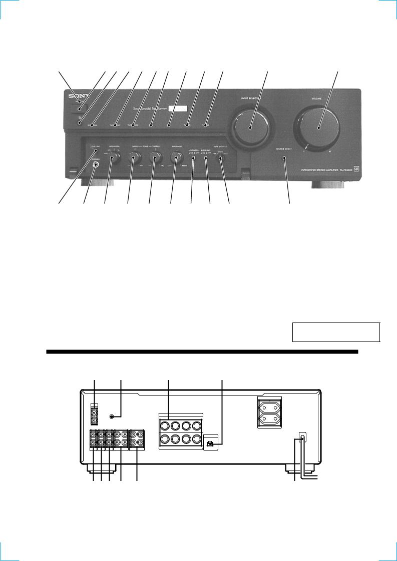
Front Panel Descriptions
1 |
2 |
3 |
4 |
5 |
6 |
7 |
8 |
9 |
10 |
11 |
12 |
|
22 |
21 |
20 |
19 |
18 |
17 |
16 |
15 |
14 |
13 |
1 |
PROTECTION indicator |
|
|
|
|
12 |
VOLUME knob |
|
||
2 |
POWER button |
|
|
|
|
|
13 |
SOURCE DIRECT button and indicator |
||
3 |
Remote sensor |
|
|
|
|
|
14 |
TAPE MONITOR knob |
|
|
4 |
EON LINK indicator |
|
|
|
|
15 |
SUBSONIC button |
|
||
5 |
TAPE 1/DAT indicator |
|
|
|
|
16 |
LOUDNESS button |
|
||
6 |
TAPE 2/MD indicator |
|
|
|
|
17 |
BALANCE knob |
|
||
7 |
AUX indicator |
|
|
|
|
|
18 |
TREBLE knob |
|
|
8 |
SACD/CD indicator |
|
|
|
|
19 |
BASS knob |
|
||
9 |
TUNER indicator |
|
|
|
|
|
20 |
SPEAKERS knob |
|
|
10 |
PHONO indicator |
|
|
|
|
|
21 |
PHONE jack |
|
|
11 |
INPUT SELECTOR knob |
|
|
|
|
22 |
EON LINK button |
|
||
This section is extracted from instruction manual.
Rear Panel Descriptions |
|
|
|
|
||
1 |
2 |
3 |
|
4 |
5 |
|
|
|
|
|
|
|
AC OUTLET |
|
|
|
|
|
|
SWITCHED 100W MAX |
PHONO |
|
|
|
|
IMPEDANCE USE 4–16Ω |
|
IN |
SIGNAL |
|
|
|
|
|
|
GND |
|
|
|
A+B USE 8–16Ω |
|
L |
U |
|
|
|
BI WIRE USE 4–16Ω |
|
|
|
SPEAKERS |
|
|||
|
|
|
|
|
||
R |
|
+ |
R |
– |
– L + |
|
|
|
B |
|
|
|
|
L |
|
|
|
|
L |
|
EON CONTROL |
|
|
|
|
|
|
|
|
|
|
|
|
|
A |
|
|
R |
|
|
|
|
R |
|
|
IN |
IN |
IN |
REC OUT IN |
REC OUT IN |
+ R – |
– L |
+ |
TUNER |
SACD/ |
AUX |
TAPE2/MD |
TAPE1/DAT |
|
|
IN |
CD |
|
|
|
qa 09 8 7 |
|
6 |
|
1 PHONO |
4 EON CONTROL IN |
6 Mains lead |
9 AUX |
2 U (SIGNAL GND) |
5 AC OUTLET |
7 TAPE1/DAT |
0 SACD/CD |
3 SPEAKERS A/B |
(Except UK, Singapore, Malaysia) |
8 TAPE2/MD |
qa TUNER |
3

SECTION 2
ELECTRICAL ADJUSTMENT
Bias Adjustment
NOTE:
1.Perform the adjustment after the unit has warmed up sufficiently.
2.Perform the bias adjustment if the power transistor has been replaced.
Procedure:
1.Rotate fully the bias adjusting semi-fixed resistors (RV500, RV600) to the MIN position (counterclockwise).
2.Connect a digital voltmeter to the CN500 and CN600.
|
1 pin |
2 pin |
CN500 (L-CH) |
+ |
– |
CN600(R-CH) |
+ |
– |
|
|
|
3.Set the slide regulator to 0V, and press the POWER button (ON) on the set.
4.Raise gradually the slide regulator voltage up to the rated voltage.
5.At this time, confirm that the SP relay is turned on (it will click).
6.Adjust the RV500 and RV600 so that a reading of digital voltmeter is 7 ± 1 mV.
7.Return the slidack to 0 V, and press the POWER button (OFF) on the set.
Adjustment Location :
[MAIN BOARD] – COMPONENT SIDE –
1 2
CN500
(L-CH)
RV500
Bias (L-CH)
RV600
Bias (R-CH)
2 1 CN600 (R-CH)
+ |
+ |
DIGITAL |
DIGITAL |
VOLTMETER |
VOLTMETER |
4
SECTION 3
DIAGRAMS
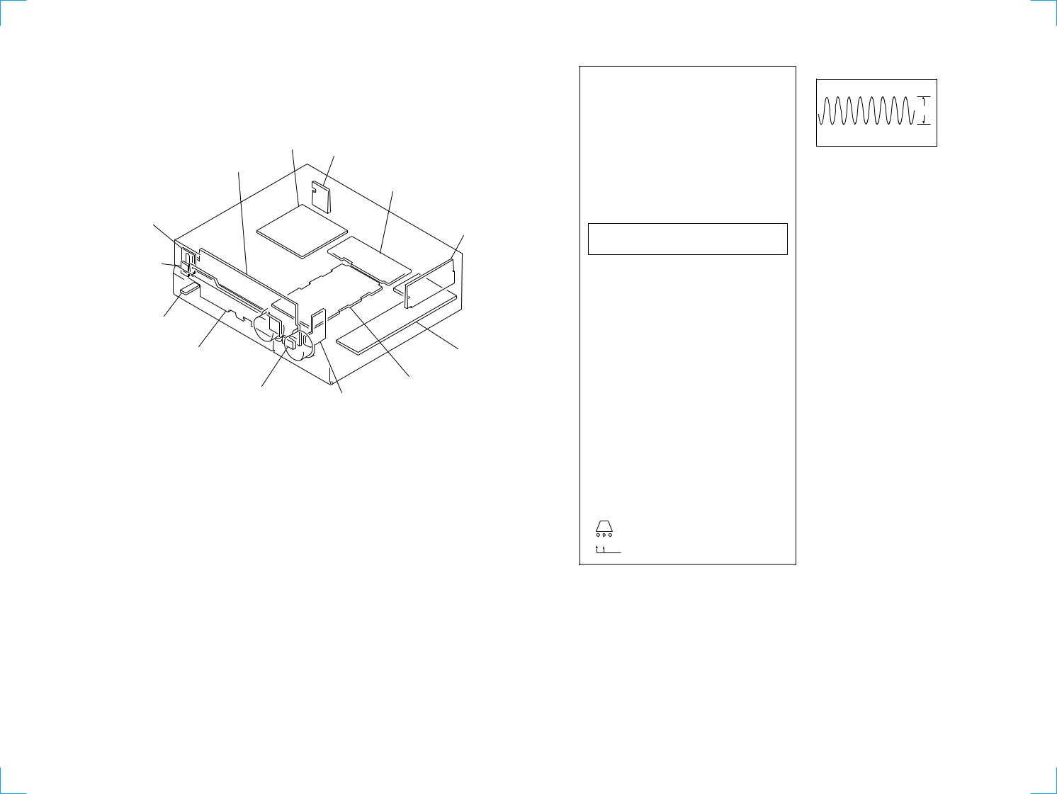
3-1. CIRCUIT BOARDS LOCATION
PS board |
OUTLET board |
|
(EXCEPT UK, SP, MY) |
PANEL board |
|
|
SP-TM board |
SIRCS board
PHONO board
SIRCS SUB board
HP board
TONE board |
INPUT board |
|
|
|
MAIN board |
|
S-D LED board |
|
VOL board |
THIS NOTE IS COMMON FOR PRINTED WIRING BOARDS AND SCHEMATIC DIAGRAMS.
(In addition to this, the necessary note is printed in each block.)
For schematic diagrams.
Note:
•All capacitors are in µF unless otherwise noted. pF: µµF 50 WV or less are not indicated except for electrolytics and tantalums.
•All resistors are in Ω and 1/4 W or less unless otherwise specified.
•f : internal component.
•2: nonflammable resistor.
•5: fusible resistor.
•C: panel designation.
Note: The components identified by mark 0or dotted line with mark 0are critical for safety.
Replace only with part number specified.
•U : B+ Line.
•V : B– Line.
•H: adjustment for repair.
•Voltages and waveforms are dc with respect to ground under no-signal (detuned) conditions.
no mark : POWER ON
•Voltages are taken with a VOM (Input impedance 10 MΩ). Voltage variations may be noted due to normal production tolerances.
•Waveforms are taken with a oscilloscope.
Voltage variations may be noted due to normal production tolerances.
•Circled numbers refer to waveforms.
•Signal path.
F : TUNER
•Abbreviation
G : German model.
EE : East European model.
AUS : Australian model.
SP |
: Singapore model. |
MY |
: Malaysia model. |
For printed wiring boards.
Note:
•X: parts extracted from the component side.
•Y: parts extracted from the conductor side.
•b: Pattern from the side which enables seeing.
•Indication of transistor
BC E
These are omitted
TA-FB940R
WAVEFORM
1
3.8Vp-p
4MHz
IC902 1 XOUT
5 5
TA-FB940R |
|
|
|
|
|
|
|
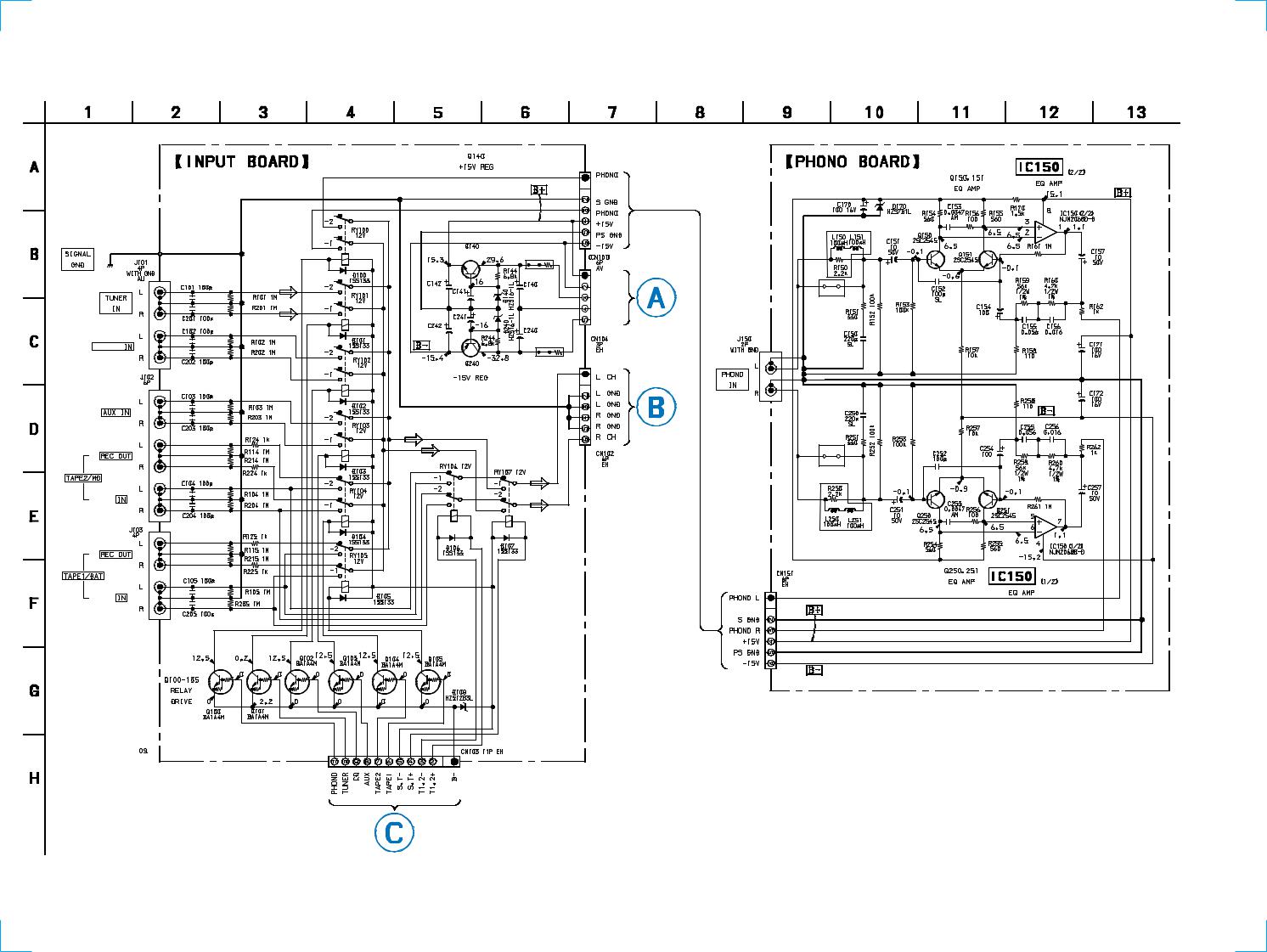
3-2. SCHEMATIC DIAGRAM – INPUT SECTION – |
|
|
|
|
|
|
|
|
|
|
|
|
|
EXCEPT |
UK, SP, MY |
|
|
2SD2525 |
|
|
|
|
|
*C101 – 105, 201 – 205 |
|
|
0R140 |
+15V |
|
|
|
EXCEPT UK, SP, MY |
|
|
|
|
|||
|
|
|
|
82 |
–15V |
|
|
* |
470 |
|
10 |
1W |
JW11 |
|
|
|
16V |
22 |
63V |
|
+B |
|
|
|
|
UK, SP, MY |
|||||
|
|
25V |
|
|
GND |
||
|
|
|
|
|
MODEL |
|
|
* |
|
22 |
|
|
–B |
|
16V |
|
|
|
|
(Page 8) |
|
|
|
* |
470 |
25V |
10 |
|
|
|
|
|
16V |
|
|
|
|
||
SACD/CD |
|
|
63V |
|
|
|
|
|
|
|
|
|
|
|
|
* |
|
|
0R240 |
|
|
|
|
|
|
2SB1640 |
|
82 |
|
|
|
|
|
|
|
1W |
|
|
|
* |
|
|
|
|
|
|
|
* |
|
|
|
|
(Page 10) |
UK, SP, MY |
|
|
|
|
|
|
|||
|
|
|
|
|
MODEL |
|
|
|
|
|
|
|
|
JW12 |
|
|
|
|
|
|
|
|
16V |
* |
|
|
|
|
|
|
|
* |
|
|
|
|
|
|
|
|
|
|
|
|
|
EXCEPT |
UK, SP, MY |
* |
|
|
|
|
|
|
|
* |
|
|
|
|
|
|
|
|
(Page 10) |
|
|
|
|
|
|
|
|
|
|
6 |
6 |
|
|
TA-FB940R
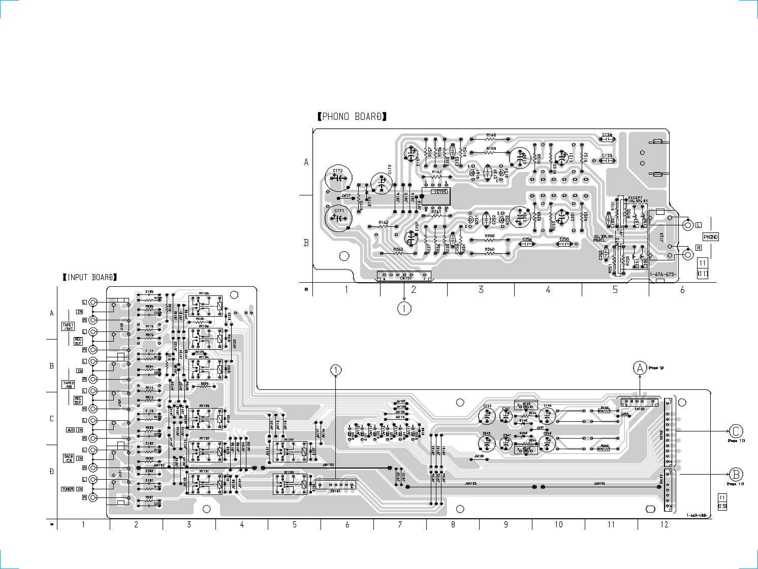
3-3. PRINTED WIRING BOARD – INPUT SECTION – • See page 5 for Circuit Boards Location.
• Semiconductor |
• Semiconductor |
Location |
Location |
(INPUT Board) |
(PHONO Board) |
Ref. No. |
Location |
|
|
D100 |
D-5 |
D101 |
D-4 |
D102 |
D-4 |
D103 |
C-4 |
D104 |
B-4 |
D105 |
A-4 |
D106 |
A-4 |
D107 |
D-5 |
D108 |
C-7 |
D140 |
C-9 |
D240 |
C-9 |
Q100 |
C-6 |
Q101 |
C-6 |
Q102 |
C-6 |
Q103 |
C-7 |
Q104 |
C-7 |
Q105 |
C-7 |
Q140 |
C-9 |
Q240 |
D-9 |
|
|
Ref. No. |
Location |
|
|
D170 |
B-1 |
IC150 |
A-2 |
Q150 |
A-3 |
Q151 |
A-3 |
Q250 |
B-3 |
Q251 |
B-3 |
|
|
*C101 – 105, 201 – 205 EXCEPT UK, SP, MY
*
*
* 
*
* 
*
*
*
*
*
7 7

TA-FB940R
3-4. SCHEMATIC DIAGRAM – MAIN SECTION – • See page 14 for IC Block Diagrams.
8 |
8 |
* |
* |
* |
* |
* |
* |
* C511, 512, 611, 612 * 
 R533, 534, 633, 634 EXCEPT UK, SP, MY
*
 Loading...