


 Loading...
TA-VE150
SERVICE MANUAL
AEP Model
UK Model
This amplifier has the Dolby Surround system. Manufactured under license from Dolby Laboratories Licensing Corporation.
“Dolby”, the double-D symbol aand “Pro Logic” are trademarks of Dolby Laboratories Licensing Corporation.
SPECIFICATIONS
Amplifier section |
|
|
Outputs |
VIDEO (AUDIO OUT): |
Power output |
|
|
|
Voltage 200 mV, |
|
|
|
|
Inpedance 10 kilohms |
Stereo mode |
(DIN 1 kHz, 8 ohms) |
|
WOOFER/AUDIO OUT: |
|
|
25 W + 25 W |
|
Voltage: 2 V |
|
|
|
|
|
Impedance: 1 kilohms |
Surround mode |
(DIN 1 kHz, 8 ohms) |
|
|
|
|
Front: 25 W/ch |
Muting |
Full mute |
|
|
Centre: 25 W |
|
+9 dB at 70 Hz |
|
|
Rear: 25 W/ch |
BASS BOOST |
||
5.1 CH |
(DIN 1 kHz, 8 ohms) |
|
|
|
INPUT/DVD mode |
Front: 25 W/ch |
General |
|
|
|
Centre: 25 W |
Power requirements |
230 V AC, 50/60 Hz |
|
|
Rear: 25 W/ch |
|
|
|
|
|
|
Power consumption |
115 W |
Frequency response |
TV, VIDEO, DVD-2CH, |
|
430 × 274 × 64.5 mm |
|
|
5.1 CH INPUT/DVD: |
Dimensions |
||
|
20 Hz-50 kHz ± 1 dB |
|
|
|
|
|
|
Mass (Approx.) |
5.4 kg |
Inputs |
|
|
|
|
|
|
|
Supplied accessories |
Remote controller |
|
Sensitivity Impedance S/N |
|||
|
|
(remote) (1) |
||
|
(weighting network, input level) |
|
Size AA (R6) batteries (2) |
|
|
|
|
|
Scart adaptor (1) |
|
|
|
|
|
TV, VIDEO, DVD-2CH, |
200 mV |
50 |
82 dB* |
|
5.1 CH INPUT/DVD |
|
kilohms |
(A, 150 mV) |
Design and specifications are subject to change without notice. |
|
|
|
|
|
|
|
|
*’78 IHF |
Specifications indicated are measured at 230 VAC, 50 HZ. |
INTEGRATED AV AMPLIFIER
MICROFILM

|
TABLE OF CONTENTS |
|
1. |
GENERAL .................................................................. |
3 |
2. |
DISASSEMBLY ......................................................... |
4 |
3. |
TEST MODE .............................................................. |
5 |
4. |
DIAGRAMS ................................................................. |
6 |
4-1. Notes for Printed Wiring Board |
|
|
|
and Schematic Diagram .................................................. |
7 |
4-2. |
Printed Wiring Board – MAIN Section – ...................... |
11 |
4-3. |
Schematic Diagram – MAIN Section (1/2) – ................ |
13 |
4-4. |
Schematic Diagram – MAIN Section (2/2) – ................ |
15 |
4-5. |
Printed Wiring Boards – PANEL Section – .................. |
17 |
4-6. |
Schematic Diagram – PANEL Section – ....................... |
19 |
4-7. |
Printed Wiring Boards – POWER Section – ................. |
21 |
4-8. |
Schematic Diagram – POWER Section – ..................... |
23 |
4-9. IC Pin Function Description ........................................... |
25 |
|
5. |
EXPLODED VIEWS ................................................ |
27 |
6. |
ELECTRICAL PARTS LIST ............................... |
29 |
Notes on chip component replacement
• Never reuse a disconnected chip component.
• Notice that the minus side of a tantalum capacitor may be damaged by heat.
SAFETY-RELATED COMPONENT WARNING!!
COMPONENTS IDENTIFIED BY A !MARK ON THE SCHEMATIC
DIAGRAMS, EXPLODED VIEWS AND IN THE PARTS LIST ARE
CRITICAL TO SAFE OPERATION. REPLACE THESE COMPO-
NENTS WITH SONY PARTS WHOSE PART NUMBERS APPEAR
AS SHOWN IN THIS MANUAL OR IN SUPPLEMENTS PUB-
LISHED BY SONY.
– 2 –

SECTION 1
GENERAL
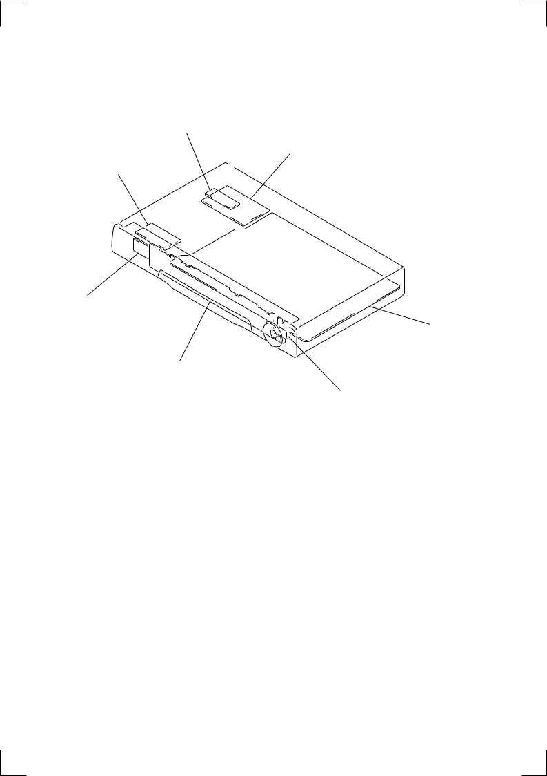
Location of controls
— Front view —
1 |
2 3 4 5 6 |
7 8 9 !º !¡ !™ |
!£ |
|||||||||||||
|
|
|
|
|
|
|
|
|
|
|
|
|
|
|
|
|
|
|
|
|
|
|
|
|
|
|
|
|
|
|
|
|
|
|
|
|
|
|
|
|
|
|
|
|
|
|
|
|
|
|
|
|
|
|
|
|
|
|
|
|
|
|
|
|
|
|
|
|
|
|
|
|
|
|
|
|
|
|
|
|
|
|
|
|
|
|
|
|
|
|
|
|
|
|
|
|
|
|
!¢ |
! |
!§ |
!¶ |
!• |
!ª |
||||||
1 |
I /ubutton |
!¡ |
BASS BOOST indicator |
|
|
|||||||
2 |
3 STEREO indicator |
|
!™ |
MUTING indicator |
|
|
||||||
3 |
NORMAL indicator |
!£ |
MASTER VOLUME dial |
|
|
|||||||
4 |
WIDE indicator |
!¢ |
CENTER MODE button |
|
|
|||||||
5 |
PHANTOM indicator |
|
! |
TV button |
|
|
|
|
||||
6 |
Remote sensor |
!§ |
VIDEO button |
|
|
|
|
|||||
7 |
Display window |
|
!¶ DVD, 2 CH button |
|
|
|||||||
8 |
SIMULATED indicator |
|
!• 5.1 CH INPUT, DVD button |
|
|
|||||||
9 |
C. STUDIO indicator |
!ª |
SURROUND MODE button |
|
|
|||||||
!º |
PRO LOGIC indicator |
|
|
|
|
|
|
|
|
|
|
|
— Rear view —
|
|
|
|
|
|
|
|
|
|
|
|
|
|
|
|
|
|
|
|
|
|
|
|
|
|
|
|
|
|
|
|
|
|
|
|
|
|
|
|
|
|
|
|
|
|
1 |
2 3 4 |
5 |
6 |
7 8 |
|||||||||
1 |
5.1 CH INPUT/DVD jacks |
|
|
5 |
WOOFER jack |
|
|
|
|
|||||
2 |
DVD 2 CH jacks |
|
|
6 |
FRONT SPEAKERS terminals |
|||||||||
3 |
VIDEO jacks |
|
|
7 |
REAR SPEAKERS terminals |
|||||||||
4 |
TV jacks |
|
|
|
|
|
|
8 |
CENTER SPEAKER terminals |
|||||
– 3 –

SECTION 2
DISASSEMBLY
Note: Follow the disassembly procedure in the numerical order given.
CASE, FRONT PANEL SECTION
3 case
1 tapping screws
1 two tapping screws
2 open the case
4flat wire (CNS301)
6 claw
1 two tapping screws
7 front panel section |
4 flat wire |
(CNS302) |
6 claw
5 three screws (BVTP3 x8)
MAIN BOARD
|
|
1 connector |
|
1 connector |
(CNS801) |
|
|
|
|
(CNP802) |
4 six screws |
|
|
|
1 connector |
(BVTP3 x8) |
|
|
||
|
(CNS800) |
|
5 Remove the |
|
A |
MAIN board |
|
|
to direction of |
|
|
the arrow A |
3 DC fan |
|
|
|
|
|
|
2 two screws |
|
|
(BVTP3 x8) |
4 six screws (BVTP3 x8)
– 4 –

SECTION 3
TEST MODE
This equipment is provided with a test mode built in the microcomputer. The contents are described in the following.
[Initial Mode]
1.Press I/u button while pressing both [VIDEO] and [5.1CH INPUT, DVD] buttons simultaneously.
2.“INITIAL” is displayed on the fluorescent indicator tube, and the status of the unit is set in the following.
•All Memory is clear.
•Center, rear level set to 0.
•Center mode set to Phantom.
•DBFB clear.
•Muting clear.
•Volume level set to min.
[Factory Mode]
1.Press I/u button while pressing three buttons of [TV],
[DVD, 2CH], and [5.1CH INPUT, DVD] simultaneously.
2.Factory setting same as initial except center mode set to normal using jog can set to volume max or min directly.
[FL Check Mode]
1.Press I/u button while both [CENTER MODE] and [VIDEO] buttons simultaneously.
2.Fluorescent indicator tube and LED are checked, “FINISH” is displayed and the status of the unit is set back in normal condition.
[Gain Up Mode]
1.Press I/u button while pressing [SURROUND MODE] button.
2.“GAIN UP” is displayed on the fluorescent indicator tube and the rear is gained up 3 dB.
3.To exit from this mode, press two buttons in the same manner as step1.
“NORMAL” is displayed on the fluorescent indicator tube and the status of the unit is set back in normal condition.
[Version Mode]
1.Press I/u button while pressing both [CENTER MODE] and [SURROUND MODE] buttons simultaneously.
2.Version of its destination is displayed on the fluorescent indicator tube.
– 5 –
SECTION 4
DIAGRAMS
• Circuit Boards Location
PRIMARY board
STANDBY board
SECONDARY board
POWER SW borad
MAIN board
DISPLAY board
JOG board
– 6 –

4-1. NOTES FOR PRINTED WIRING BOARD AND SCHEMATIC DIAGRAM
Note on Schematic Diagram:
•All capacitors are in µF unless otherwise noted. pF: µµF 50 WV or less are not indicated except for electrolytics and tantalums.
•All resistors are in Ω and 1/4 W or less unless otherwise specified.
•¢ : internal component.
•2 : nonflammable resistor.
•C : panel designation.
Note: The components identified by mark !or dotted line with mark !are critical for safety.
Replace only with part number specified.
•U : B+ Line.
•V : B– Line.
•Voltages and waveforms are dc with respect to ground under no-signal conditions.
no mark : VIDEO
•Voltages are taken with a VOM (Input impedance 10 MΩ).
Voltage variations may be noted due to normal production tolerances.
•Waveforms are taken with a oscilloscope.
Voltage variations may be noted due to normal production tolerances.
•Circled numbers refer to waveforms.
•Signal path.
F : FRONT/AUDIO IN f : REAR
E : CENTER j : WOOFER
Note on Printed Wiring Board:
•X : parts extracted from the component side.
•p : parts mounted on the conductor side.
•b : Pattern from the side which enables seeing.
•Indication of transistor.
C 
|
|
|
|
|
|
|
|
|
|
|
|
|
|
Q |
|
|
These are omitted. |
||||
|
|
|
|
|
||||||
B E
Q
B C E
These are omitted.
– 7 –

• Waveforms
– MAIN Board –
1 IC300 #¡ (OSC)
3.4 Vp-p
8MHz
–DISPLAY Board –
1 IC201 #¢ (X1)
4.3 Vp-p
4.19 MHz
– 8 –
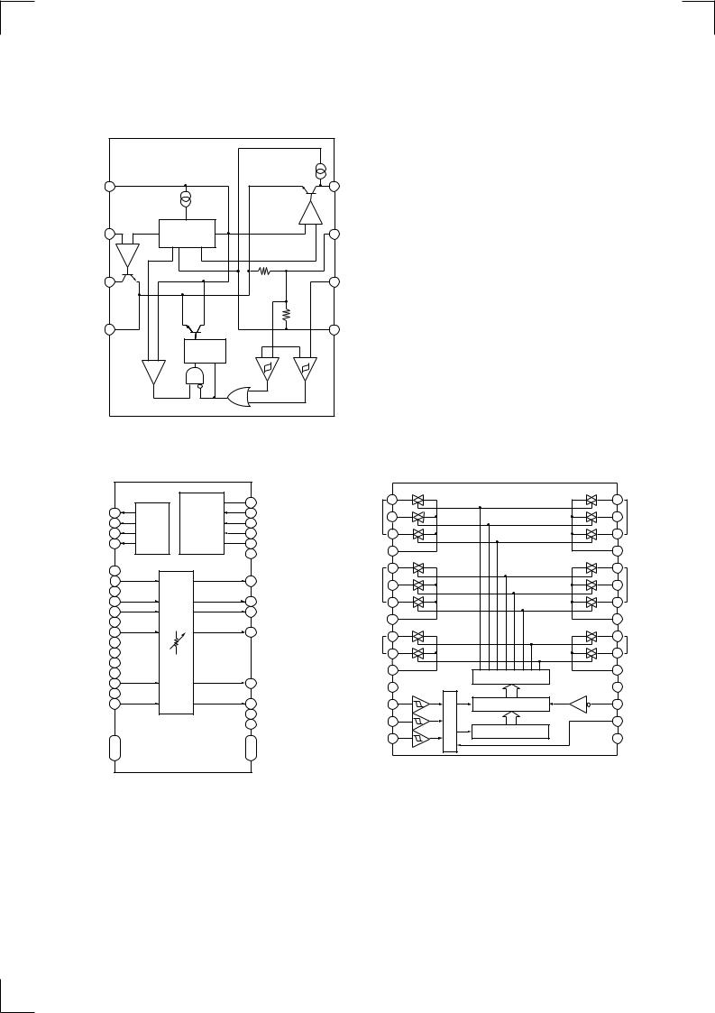
• IC Block Diagrams
– STANDBY Board –
IC950 |
NJM2103D |
|
|
|
|
|
|
||
CR |
1 |
|
|
|
|
|
|
8 |
RESET |
|
|
|
|
|
|
|
– |
+ |
|
VSC |
2 |
|
VREF |
|
|
|
|
7 |
VSA |
|
|
+ |
– |
|
|
|
|
|
|
OUTC |
3 |
|
|
|
|
|
|
6 |
VSB/SESIN |
GND |
4 |
|
|
|
|
|
|
5 |
V+ |
|
|
|
Q |
|
|
|
|
|
|
|
|
|
R |
S |
+ |
– |
+ |
– |
|
|
|
|
|
|
|
||||
– MAIN Board – |
|
|
|
||
IC100 |
|
M62447SP |
|
|
|
|
|
|
|
42 |
DVDD |
OUT4 |
1 |
|
MICRO |
41 |
CLK |
OUT3 |
2 |
OUTPUT |
COMPUTER |
40 |
DATA |
OUT2 |
3 |
PORT |
INTERFACE |
39 |
LATCH |
OUT1 |
4 |
|
|
38 |
DGND |
|
|
|
|
37 |
AGND |
AVDD |
5 |
|
|
|
|
SW IN |
6 |
|
|
36 |
SW OUT |
GND S |
7 |
|
|
|
|
SR IN |
8 |
|
|
35 |
SR OUT |
SL IN |
9 |
|
|
34 |
SL OUT |
GND C |
10 |
|
|
|
|
C IN |
11 |
|
|
33 |
C OUT |
GND R1 |
12 |
|
|
|
|
GND R2 |
13 |
|
|
|
|
GND L1 |
14 |
|
|
|
|
GND L2 |
15 |
|
|
|
|
R IN |
16 |
|
|
32 |
R OUT |
GND LR |
17 |
|
|
|
|
L IN |
18 |
|
|
31 |
L OUT |
|
|
|
|
30 |
AVSS1 |
|
|
|
|
29 |
AVSS2 |
NC |
21 – 19 |
|
|
22 – 28 |
NC |
IC500 LC7822
|
1 |
|
|
IN |
2 |
|
|
|
3 |
|
|
OUT |
4 |
|
|
|
5 |
|
|
IN |
6 |
|
|
|
7 |
|
|
OUT |
8 |
|
|
IN |
9 |
|
|
|
|
||
|
10 |
|
|
OUT |
11 |
|
|
VEE |
12 |
|
|
CE |
13 |
CONTROL |
|
DI |
14 |
||
|
|||
CL |
15 |
|
30 |
|
29 |
IN |
28 |
|
27 |
OUT |
26 |
|
25 IN
24
23 OUT
22 |
IN |
|
|
21 |
|
20 |
OUT |
LEVEL SHIFT
19 VDD
LATCH |
18 RESET |
17 S
SHIFT RESISTOR
16 VSS
– 9 –
Loading...