


TA-FB930R
SERVICE MANUAL
AEP Model
Photo: BLACK model
SPECIFICATIONS
INTEGRATED STEREO AMPLIFIER
MICROFILM
1

TABLE OF CONTENTS |
|
1. GENERAL .......................................................................... |
3 |
2. ELECTRICAL ADJUSTMENT ..................................... |
4 |
3. DIAGRAMS |
|
3-1. Circuit Boards Location ........................................................ |
5 |
3-2. Schematic Diagram – Input Section – .................................. |
6 |
3-3. Printed Wiring Board – Input Section – ................................ |
7 |
3-4. Schematic Diagram – Main Section – .................................. |
8 |
3-5. Printed Wiring Board – Main Section – ................................ |
9 |
3-6. Schematic Diagram – Panel Section – ................................ |
10 |
3-7. Printed Wiring Board – Panel Section – ............................. |
11 |
3-8. Schematic Diagram – Power Section – ............................... |
12 |
3-9. Printed Wiring Board – Power Section – ............................ |
13 |
3-10. IC Block Diagrams ............................................................ |
14 |
3-11. IC Pin Function ................................................................. |
14 |
4. EXPLODED VIEW |
|
4-1. Case Section ........................................................................ |
15 |
4-2. Front Panel Section ............................................................. |
16 |
4-3. Chassis Section ................................................................... |
17 |
5. ELECTRICAL PARTS LIST ........................................ |
18 |
SAFETY-RELATED COMPONENT WARNING !!
COMPONENTS IDENTIFIED BY MARK !OR DOTTED LINE WITH MARK !ON THE SCHEMATIC DIAGRAMS AND IN
THE PARTS LIST ARE CRITICAL TO SAFE OPERATION. REPLACE THESE COMPONENTS WITH SONY PARTS WHOSE PART NUMBERS APPEAR AS SHOWN IN THIS MANUAL OR IN SUPPLEMENTS PUBLISHED BY SONY.
2
SECTION 1
GENERAL
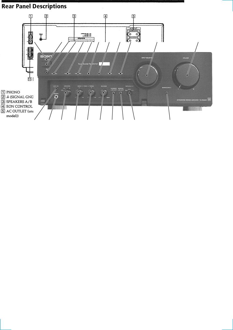
Front Panel Descriptions
1 |
2 |
3 |
4 |
5 |
6 |
7 |
8 |
9 |
10 |
11 |
12 |
|
22 |
21 |
20 |
19 |
18 |
17 |
16 |
15 |
14 |
13 |
|
1 |
PROTECTION indicator |
|
|
|
|
12 |
VOLUME knob |
|
|
||
2 |
U(Power) button |
|
|
|
|
|
13 |
SOURCE DIRECT button and indicator |
|||
3 |
Remote sensor |
|
|
|
|
|
14 |
TAPE MONITOR knob |
|
|
|
4 |
EON LINK indicator |
|
|
|
|
15 |
SUBSONIC button |
|
|
||
5 |
TAPE 1/DAT indicator |
|
|
|
|
16 |
LOUDNESS button |
|
|
||
6 |
TAPE 2/MD indicator |
|
|
|
|
17 |
BALANCE knob |
|
|
||
7 |
AUX indicator |
|
|
|
|
|
18 |
TREBLE knob |
|
|
|
8 |
CD indicator |
|
|
|
|
|
19 |
BASS knob |
|
|
|
9 |
TUNER indicator |
|
|
|
|
|
20 |
SPEAKERS knob |
|
|
|
10 |
PHONO indicator |
|
|
|
|
|
21 |
PHONE jack |
|
|
|
11 |
INPUT SELECTOR knob |
|
|
|
|
22 |
EON LINK button |
|
|
||
|
|
|
|
|
|
|
|
|
|
|
|
|
|
|
|
|
|
|
|
|
|
|
This section is extracted from |
|
|
|
|
|
|
|
|
|
|
|
instruction manual. |
|
|
|
|
|
|
|
|
|
|
|
|
3
SECTION 2
ELECTRICAL ADJUSTMENT
Bias Adjustment
NOTE:
1.Perform the adjustment after the unit has warmed up sufficiently.
2.Perform the bias adjustment if the power transistor has been replaced.
Procedure:
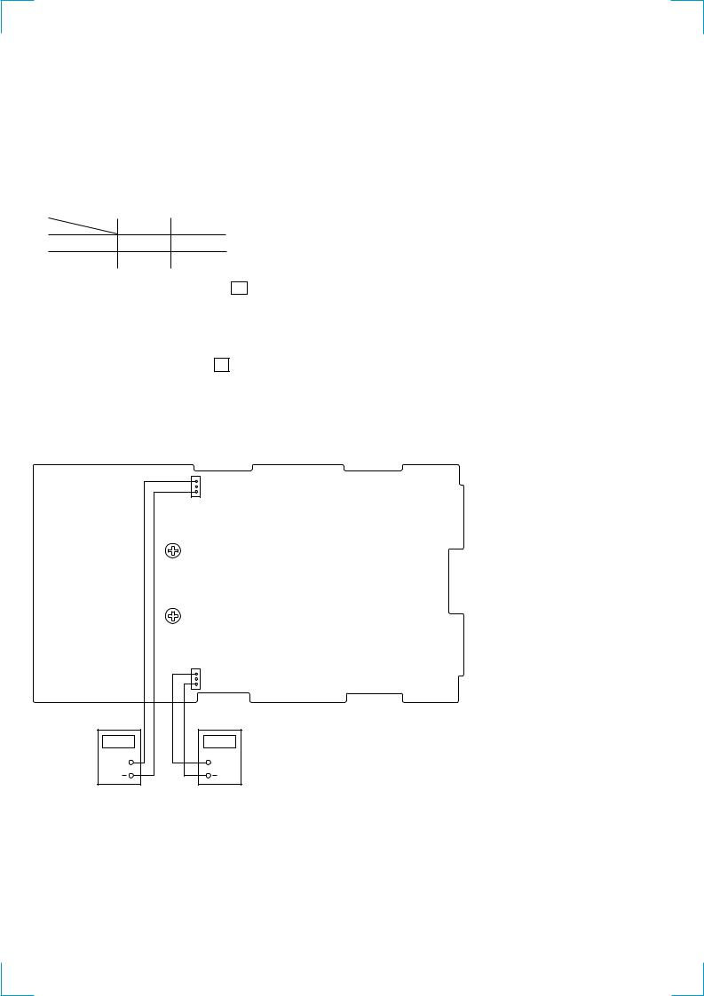
1.Rotate fully the bias adjusting semi-fixed resistors (RV500, RV600) to the MIN position (counterclockwise).
2.Connect a digital voltmeter to the CN500 and CN600.
|
1 pin |
3 pin |
CN500 (L-CH) |
+ |
– |
CN600(R-CH) |
+ |
– |
|
|
|
3.Set the slide regulator to 0V, and press the U button (ON) on the set.
4.Raise gradually the slide regulator voltage up to the rated voltage.
5.At this time, confirm that the SP relay is turned on (it will click).
6.Adjust the RV500 and RV600 so that a reading of digital voltmeter is 10 ± 1 mV.
7.Return the slidack to 0 V, and press the U button (OFF) on the set.
Adjustment Location :
[MAIN BOARD] – COMPONENT SIDE –
1
3
CN500 (L-CH)
RV500
Bias (L-CH)
RV600
Bias (R-CH)
CN600 (R-CH) 1 3
+ |
+ |
DIGITAL |
DIGITAL |
VOLTMETER |
VOLTMETER |
4

SECTION 3
DIAGRAMS
3-1. CIRCUIT BOARDS LOCATION
PS board OUTLET board
PANEL board
SP-TM board
SIRCS board
PHONO board
SIRCS SUB board
HP board
TONE board |
INPUT board |
|
|
|
MAIN board |
|
S-D LED board |
|
VOL board |
THIS NOTE IS COMMON FOR PRINTED WIRING BOARDS AND SCHEMATIC DIAGRAMS.
(In addition to this, the necessary note is printed in each block.)
For schematic diagrams.
Note:
•All capacitors are in µF unless otherwise noted. pF: µµF 50 WV or less are not indicated except for electrolytics and tantalums.
•All resistors are in Ω and 1/4 W or less unless otherwise specified.
•¢ : internal component.
•2: nonflammable resistor.
•5: fusible resistor.
•C : panel designation.
Note: The components identified by mark !or dotted line with mark !are critical for safety.
Replace only with part number specified.
•U : B+ Line.
•V : B– Line.
•H: adjustment for repair.
•Voltages and waveforms are dc with respect to ground under no-signal (detuned) conditions.
no mark : POWER ON
•Voltages are taken with a VOM (Input impedance 10 MΩ). Voltage variations may be noted due to normal production tolerances.
•Waveforms are taken with a oscilloscope.
Voltage variations may be noted due to normal production tolerances.
•Circled numbers refer to waveforms.
•Signal path.
F : TUNER
•Abbreviation
G : German model.
EE : East European model.
AUS : Australian model.
SP |
: Singapore model. |
MY |
: Malaysia model. |
For printed wiring boards.
Note:
•X : parts extracted from the component side.
•Y : parts extracted from the conductor side.
•b: Pattern from the side which enables seeing.
•Indication of transistor
BC E
 These are omitted
WAVEFORM
1
3.8Vp-p
4MHz
IC902 1 XOUT
5 5
TA-FB930R |
|
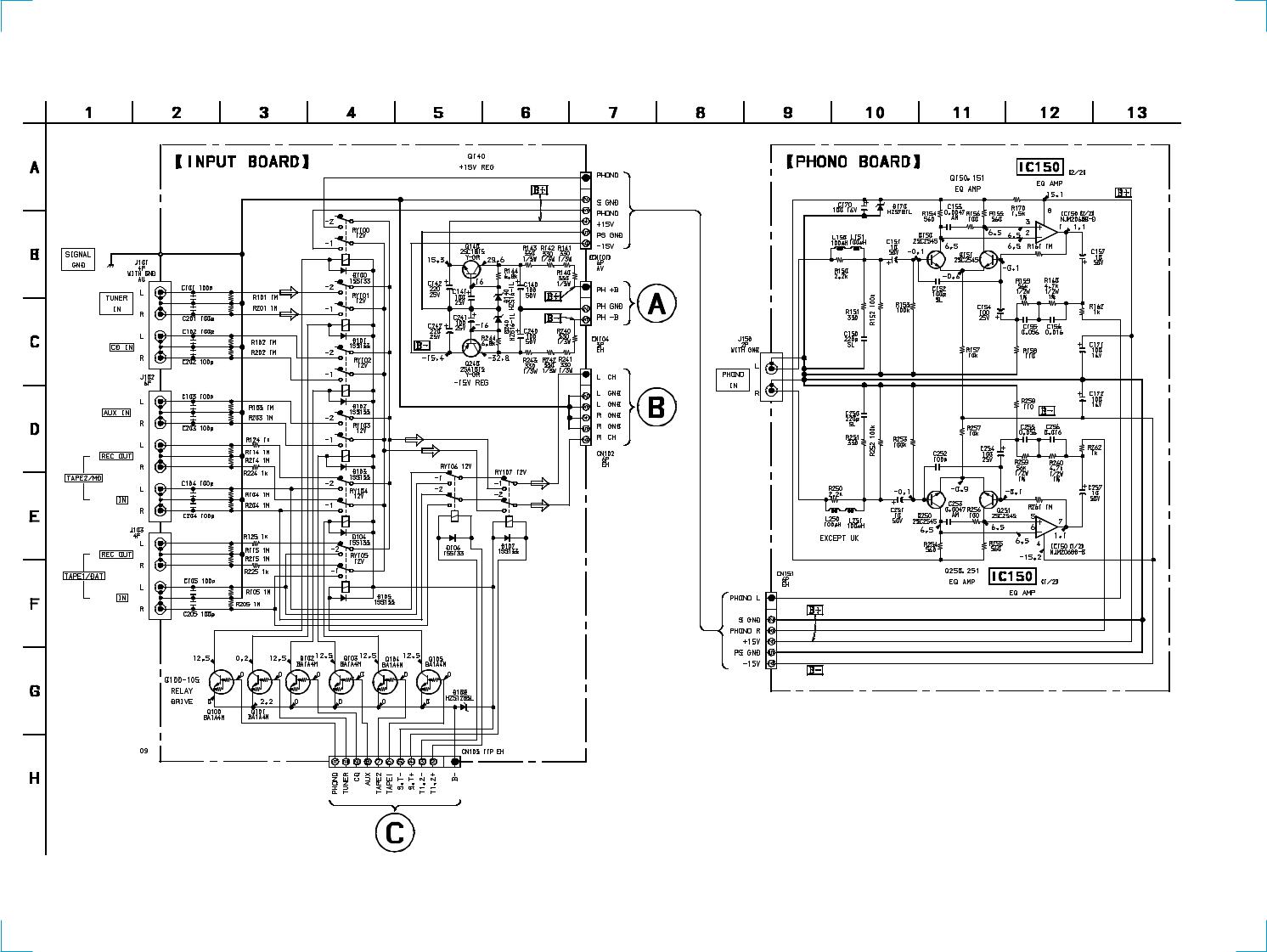
3-2. SCHEMATIC DIAGRAM – INPUT SECTION – |
|
|
(Page 8) |
|
(Page 10) |
(Page 10) |
|
6 |
6 |
TA-FB930R
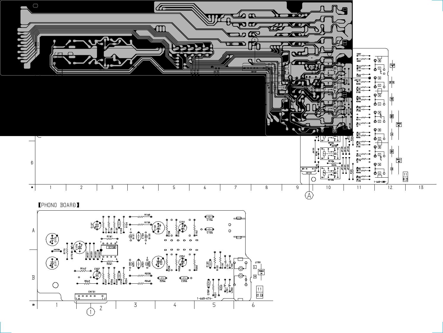
3-3. PRINTED WIRING BOARD – INPUT SECTION –
• See page 5 for Circuit Boards Location.
 (Page 11) (Page 11)
(Page 9)
• Semiconductor
Location
Ref. No. |
Location |
|
|
D100 |
A-8 |
D101 |
A-10 |
D102 |
B-10 |
D103 |
B-10 |
D104 |
C-10 |
D105 |
D-10 |
D106 |
D-10 |
D107 |
B-8 |
D108 |
B-6 |
D140 |
B-4 |
D240 |
B-4 |
Q100 |
B-7 |
Q101 |
B-7 |
Q102 |
B-7 |
Q103 |
B-7 |
Q104 |
B-6 |
Q105 |
B-6 |
Q140 |
C-4 |
Q240 |
B-4 |
|
|
7 7

TA-FB930R
3-4. SCHEMATIC DIAGRAM – MAIN SECTION –
• See page 14 for IC Block Diagrams.
(Page 10) |
|
(Page 10) |
|
(Page |
(Page 12) |
12) |
|
|
(Page |
|
10) |
|
(Page 6) |
8 |
8 |
 Loading...