Sony STR-KS370, STR-SK370 Schematic

STR-KS370
pp
SERVICE MANUAL
Ver. 1.0 2010.01
This receiver incorporates Dolby* Digital and Pro
Logic Surround and the DTS** Digital Surround
System.
* Manufactured under license from Dolby
Laboratories. Dolby, Pro Logic, and the doubleD symbol are trademarks of Dolby Laboratories.
** Manufactured under license under U.S. Patent
#’s: 5,451,942; 5,956,674; 5,974,380;
5,978,762; 6,487,535 & other U.S. and
worldwide patents issued & pending. DTS and
DTS Digital Surround are registered trademarks
and the DTS logos and Symbol are trademarks of
DTS, Inc. © 1996-2008 DTS, Inc. All Rights
Reserved.
This receiver incorporates High-Definition
Multimedia Interface (HDMI
HDMI, the HDMI logo and High-Definition
Multimedia Interface are trademarks or registered
trademarks of HDMI Licensing LLC in the
United States and other countries.
“x.v.Color” and “x.v.Color”
Sony Corporation.
“BRAVIA” is a trademark of Sony Corporation.
“PlayStation” is a registered trademark of Sony
Computer Entertainment Inc.
“S-AIR” and its logo are trademarks of Sony
TM
) technology.
About area codes
The area code of the receiver you purchased is
shown on the upper left portion of the rear panel
(see the illustration below).
4-XXX-XXX-XX(X) AA
Area code
Any differences in operation, according to the area
code, are clearly indicated in the text, for example,
“Models of area code AA only”.
SPEAKERS
FRONT L SUR R SUR L CENTER
FRONT R
SUBWOOFER
AUDIO POWER
SPECIFICATIONS
Amplifier section
POWER OUTPUT AND TOTAL HARMONIC
DISTORTION:
(FTC)
(Models of area code US only)
FRONT L + FRONT R
POWER OUTPUT (reference)
FRONT L/FRONT R/CENTER/SUR L/SUR R
SUBWOOFER 165 W (at 3 ohms, 60 Hz)
Inputs
Analog Sensitivity: 1 V/50 kohms
Digital (Coaxial) Impedance: 75 ohms
FM tuner section
Tuning range 87.5 – 108.0 MHz
Antenna FM wire antenna
Antenna terminals 75 ohms, unbalanced
Intermediate frequency
AM tuner section
Tuning range
Area code Tuning scale
US 530 –
Antenna AM loop antenna
Intermediate frequency
SPECIFICATIONS
With 3 ohm loads, both
channels driven, from 180
– 20,000 Hz; rated 84 watts
per channel minimum
RMS power, with no more
than 1% total harmonic
distortion from 250
milliwatts to rated output.
167 W (per channel at
3 ohms, 1 kHz)
(100 kHz step)
7 MHz
10.
10 kHz step 9 kHz step
1,710 kHz
450 kHz
531 –
1,710 kHz
US Model
General
Power requirements
Area code Power requirements
US 120 V AC, 60 Hz
Power output (DIGITAL MEDIA PORT)
DC OUT: 5 V, 0.7A MAX
Power consumption
Area code Power consumption
US 110 W
Power consumption (during standby mode)
Dimensions (w/h/d) (Approx.)
Mass (A
Design and specifications are subject to
change without notice.
Halogenated flame retardants are not used in
the certain printed wiring boards.
0.3 W (When Control for
HDMI and S-AIR standby
are set to off)
17 in × 2 5/8 in × 12 1/8 in
(430 mm × 66.5 mm ×
306 mm)
including projecting parts
and controls
rox.) 7 lb 8 oz (3.4 kg)
AV RECEIVER
9-890-531-01
2010A08-1
2010.01
©
Sony Corporation
Audio & Video Business Group
Published by Sony EMCS (Malaysia) PG Tec
STR-KS370
NOTES ON CHIP COMPONENT REPLACEMENT
• Never reuse a disconnected chip component.
• Notice that the minus side of a tantalum capacitor may be damaged by heat.
SAFETY CHECK-OUT
After correcting the original service problem, perform the following safety check before releasing the set to the customer:
Check the antenna terminals, metal trim, “metallized” knobs,
screws, and all other exposed metal parts for AC leakage.
Check leakage as described below.
LEAKAGE TEST
The AC leakage from any exposed metal part to earth ground and
from all exposed metal parts to any exposed metal part having a
return to chassis, must not exceed 0.5 mA (500 microamperes.).
Leakage current can be measured by any one of three methods.
1. A commercial leakage tester, such as the Simpson 229 or RCA
WT-540A. Follow the manufacturers’ instructions to use these
instruments.
2. A battery-operated AC milliammeter. The Data Precision 245
digital multimeter is suitable for this job.
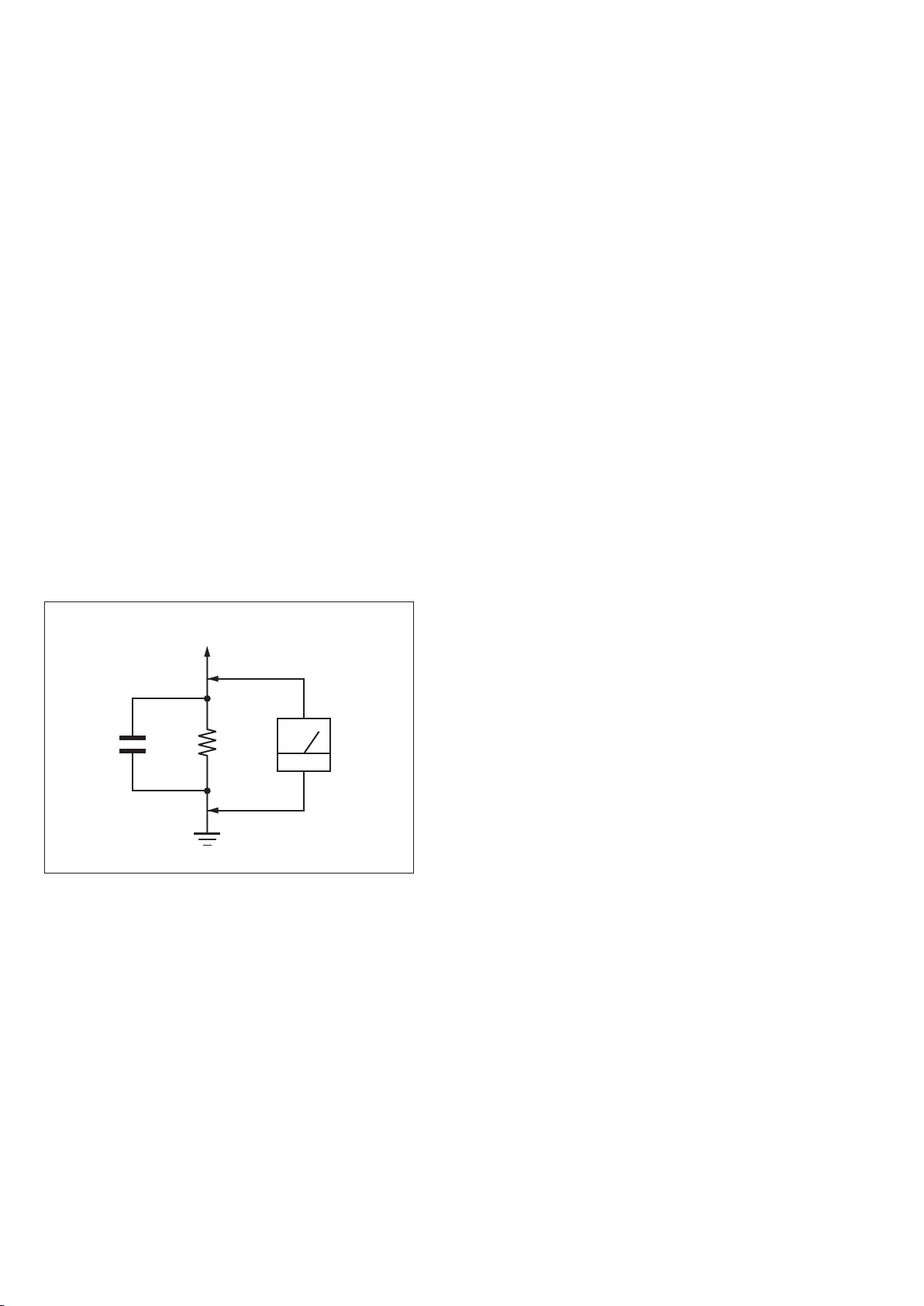
3. Measuring the voltage drop across a resistor by means of a
VOM or battery-operated AC voltmeter. The “limit” indication
is 0.75 V, so analog meters must have an accurate low-voltage
scale. The Simpson 250 and Sanwa SH-63Trd are examples
of a passive VOM that is suitable. Nearly all battery operated
digital multimeters that have a 2 V AC range are suitable. (See
Fig. A)
To Exposed Metal
Parts on Set
AC
1.5 kΩ0.15 μF
Earth Ground
Fig. A. Using an AC voltmeter to check AC leakage.
voltmeter
(0.75 V)
TABLE OF CONTENTS
1. SERVICING NOTES .............................................. 3
2. DISASSEMBLY ......................................................... 4
2-1. Disassembly Flow ........................................................... 4
2-2. Case ................................................................................. 4
2-3. S-AIR Board ................................................................... 5
2-4. Tuner (FM/AM), IO Board ............................................ 5
2-5. Front Panel Block ........................................................... 6
2-6. MAIN Board ................................................................... 6
3. TEST MODE ............................................................. 7
4. ELECTRICAL CHECK .......................................... 9
5. DIAGRAMS ................................................................ 10
5-1. Block Diagram - MAIN Section - ................................... 11
5-2. Block Diagram - HDMI PC Section - ............................. 12
5-3. Block Diagram - DSP/S-AIR Section - .......................... 13
5-4. Block Diagram- AMP Section - ...................................... 14
5-5. Block Diagram - SMPS Section - ................................... 15
5-6. Printed Wiring Board
- MAIN Board (Component Side) - ................................ 17
5-7. Printed Wiring Board
- MAIN Board (Conductor Side) - .................................. 18
5-8. Schematic Diagram - MAIN Board (1/5) - ..................... 19
5-9. Schematic Diagram - MAIN Board (2/5) - ..................... 20
5-10. Schematic Diagram - MAIN Board (3/5) - ..................... 21
5-11. Schematic Diagram - MAIN Board (4/5) - ..................... 22
5-12. Schematic Diagram - MAIN Board (5/5) - ..................... 23
5-13. Printed Wiring Board- S-AIR and IO Board - ................ 24
5-14. Schematic Diagram - S-AIR Board - .............................. 24
5-15. Schematic Diagram - IO Board - .................................... 25
5-16. Printed Wiring Board - HDMI PC Board - ..................... 26
5-17. Schematic Diagram - HDMI PC Board (1/2) - ............... 27
5-18. Schematic Diagram - HDMI PC Board (2/2) - ............... 28
5-19. Printed Wiring Board - DISPLAY, IR, LED,
KEY FUNCTION and KEY POWER Board - .............. 29
5-20. Schematic Diagram - DISPLAY, IR, LED,
KEY FUNCTION and KEY POWER Board - ............... 30
5-21. Printed Wiring Board- SMPS Board - ............................ 31
5-22. Schematic Diagram - SMPS Board - .............................. 32
6. EXPLODED VIEWS ............................................... 43
6-1. Case, S-AIR Board Section ............................................ 43
6-2. Front Panel Section ......................................................... 44
6-3. Chassis Section ............................................................... 45
SAFETY-RELATED COMPONENT WARNING!
COMPONENTS IDENTIFIED BY MARK 0 OR DOTTED LINE
WITH MARK 0 ON THE SCHEMATIC DIAGRAMS AND IN
THE PARTS LIST ARE CRITICAL TO SAFE OPERATION.
REPLACE THESE COMPONENTS WITH SONY PARTS
WHOSE PART NUMBERS APPEAR AS SHOWN IN THIS
MANUAL OR IN SUPPLEMENTS PUBLISHED BY SONY.
2
7. ELECTRICAL PARTS LIST ............................... 46

SECTION 1
SERVICING NOTES
UNLEADED SOLDER
Boards requiring use of unleaded solder are printed with the leadfree mark (LF) indicating the solder contains no lead.
(Caution: Some printed circuit boards may not come printed with
the lead free mark due to their particular size)
: LEAD FREE MARK
Unleaded solder has the following characteristics.
• Unleaded solder melts at a temperature about 40 °C higher
than ordinary solder.
Ordinary soldering irons can be used but the iron tip has to be
applied to the solder joint for a slightly longer time.
Soldering irons using a temperature regulator should be set to
about 350 °C.
Caution: The printed pattern (copper foil) may peel away if
the heated tip is applied for too long, so be careful!
• Strong viscosity
Unleaded solder is more viscous (sticky, less prone to fl ow)
than ordinary solder so use caution not to let solder bridges
occur such as on IC pins, etc.
• Usable with ordinary solder
It is best to use only unleaded solder but unleaded solder may
also be added to ordinary solder.
STR-KS370
NOTE OF REPLACING THE IC3500 AND IC3501 ON
THE HDMI PC BOARD
IC3500 and IC3501 on the HDMI PC board cannot exchange with
single. When these parts on the HDMI PC board are damaged,
exchange the entire mounted board.
3

STR-KS370
DISASSEMBLY
• This set can be disassembled in the order shown below.
2-1. DISASSEMBLY FLOW
SET
2-2. CASE
(Page 4)
SECTION 2
2-3. S-AIR BOARD
(Page 5)
2-6. MAIN BOARD
(Page 6)
Note: Follow the disassembly procedure in the numerical order given.
2-4. TUNER (FM/AM), IO BOARD
(Page 5)
2-2. CASE
2 one screw
FLAT HEAD (TP)
3
6
2-5. FRONT PANEL BLOCK
(Page 6)
7 case
1 four screws
FLAT HEAD (TP)
4 Lift up the case
in the direction of arrow.
5 two claws
3
2 one screw
FLAT HEAD (TP)
4

2-3. S-AIR BOARD
STR-KS370
5 SAIR board
4 connector (CN104)
3 two screws
+BV3 (3-CR)
6 card slot (SAIR)
2 one screw
+BV3 (3-CR)
1 four screws
+BV3 (3-CR)
2-4. TUNER (FM/AM), IO BOARD
7 IO board
6 cushion saranet
1 wire (flat type) (9 core)
(CNS250)
4 Tuner (FM/AM)
3 two screws
+BV3 (3-CR)
5 four screws
+BV3 (3-CR)
2 wire (flat type) (25 core)
(CNS200)
5
STR-KS370
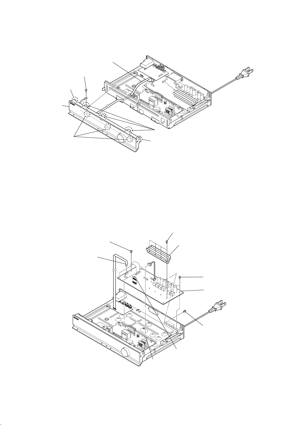
2-5. FRONT PANEL BLOCK
2 one screw
+BV3 (3-CR)
4 claw
6 front panel block
5 three claws
1 wire (flat type) (13 core)
(CNS700)
3 three claws
4 claw
2-6. MAIN BOARD
1 wire (flat type) (19 core)
(CN1007)
4 two screws
+BV3 (3-CR)
6 four screws
BVTP 3 x 14
7 heat sink (AMP)
4 two screws
+BV3 (3-CR)
8 MAIN board
5 two screws
+BV3 (3-CR)
3 connector
(CN906)
2 connector
(CN904)
6
SECTION 3
TEST MODE
STR-KS370
1. COLD RESET
All preset contents are cleared when this mode is activated. Use
this mode before returning the product to clients upon completion
of repair.
Procedure:
1. Press the [
2. Keeps pressing the [
] button on the set to turn the power on.
?/1
] button on the set for about fi ve sec-
?/1
onds.
3. The message “CLEARED” appears, then the set turns off.
2. HOW TO ENTER THE TEST MODE
Note: The operation of the button of the following test modes is only a
remote commander.
Procedure:
1. Press the [
] button to turn the power on.
?/1
2. Press the buttons in order of [TUNER] [RETURN] Hold
SHIFT button ([ENTER] [0] [1] [0]) [SOUND
FIELD +]
3. The message “TEST MENU” appears, then enter the test
menu.
4. Press the [
] button to exit from the test mode.
?/1
3. PANEL TEST
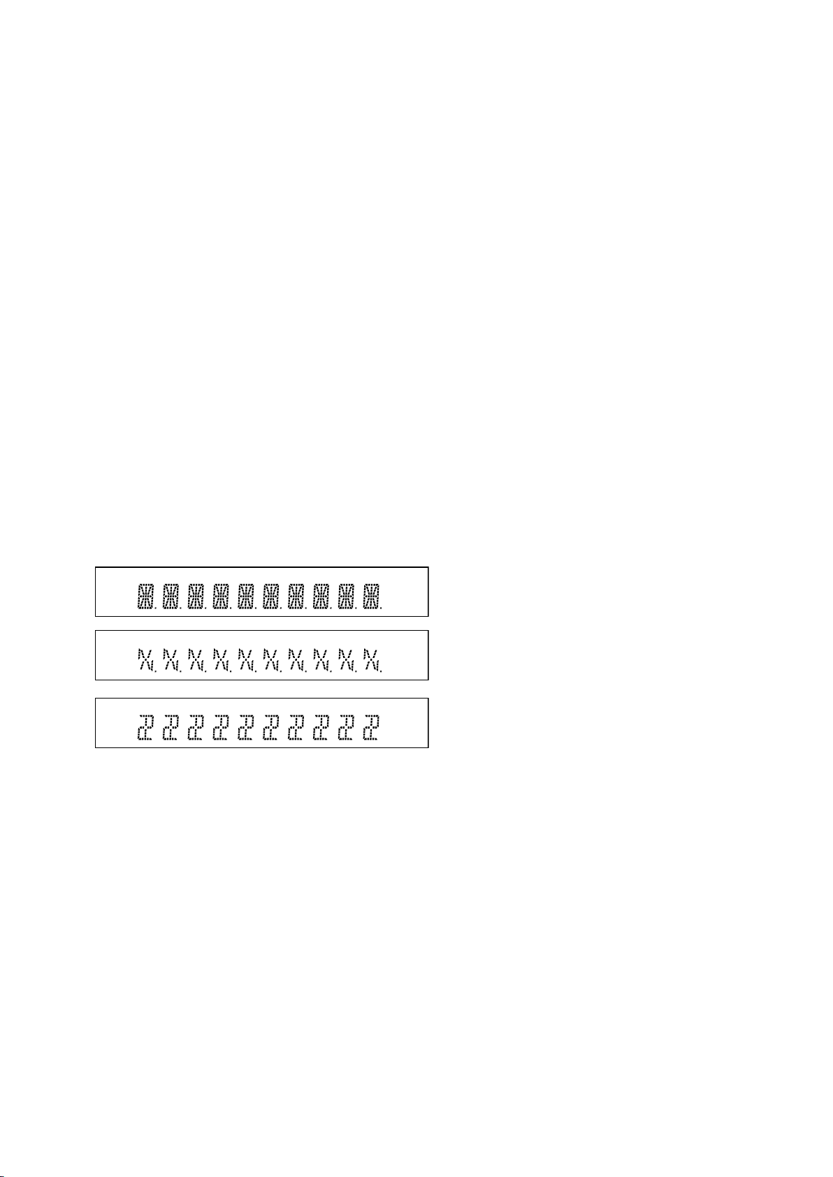
3-1. Pattern check
Procedure:
1. Enter the test mode menu.
2. Press the []/[] buttons to select “PANEL”, and press the
[ENTER] button.
3. All segments and all LEDs turn on. Change as follows all on,
test pattern 1, test pattern 2 and test pattern 3, all on in this
order.
;
;
;
;
;
;
;
;
TrueHD
D + EX
PL II x
TrueHD
D + EX
PL II x
D EX
PL II
NIGHT SLEEP HDMI COAX OPT TUNED ST S-AIR ECO MUTINGAACLPCM
NIGHT SLEEP HDMI COAX OPT TUNED ST S-AIR ECO MUTINGAACLPCM
TUNED STLPCM
DTS 96/24
-ES NEO:6
DTS -HDLBR
MSTR HI RES
DTS 96/24
-ES NEO:6
DTS -HDLBR
MSTRHI RES
DTS
NEO:6
DTS -HD
MSTR
3-2. Key check
Procedure:
1. Press the [VOLUME –] button, while executing pattern
check.
2. The message “K0 V0” appears. “K0” value increases whenever a button on the set is pressed. However, once a button has
been pressed, it is no longer taken into account. All buttons on
the set is pressed, “K3 V0” is displayed.
3. “V” value increases in the manner of 0, 1, 2, 3 ... [MASTER
VOLUME] knob is turned clockwise, or it decreases in the
manner of 0, 9, 8, 7 ... [MASTER VOLUME] knob is turned
counterclockwise.
4. Press the [
] button to exit from the test mode.
?/1
3-3. Software version and destination display
Procedure:
1. Press the [VOLUME +] button, while executing pattern
check.
2. The display of model name, destination, and software version
changes whenever [VOLUME +] button is pressed.
3. Press the [
] button to exit from the test mode.
?/1
4. AMP TEST
Not used for the servicing.
Press the [
] button if having entered this mode.
?/1
5. TUNER FACTORY PRESET
Not used for the servicing.
Press the [
] button if having entered this mode.
?/1
6. VACS DISPLAY
Procedure:
1. Enter the test mode menu.
2. Press the []/[] buttons to select “VACS DISP”, and press the
[ENTER] button.
3. It will appear the VACS status
7. VACS ON/OFF
Procedure:
1. Enter the test mode menu.
2. Press the []/[] buttons to select “VACS ON OFF”, and press
the [ENTER] button.
3. The VACS status will change.
8. DSP HALT MODE
Not used for the servicing.
Press the [
] button if having entered this mode.
?/1
9. DSP STATUS DISPLAY
Not used for the servicing.
Press the [
] button if having entered this mode.
?/1
10. HDMI UCOM UPDATE
Procedure:
1. Enter the test mode menu.
2. Press the []/[] buttons to select “HDMI VER”, and press the
[ENTER] button.
3. HDMI MICOM software version is displayed.
4. Press the [
] button to exit from the test mode.
?/1
11. HDMI THROUGH DMPORT UPDATE
Procedure:
1. Enter the test mode menu.
2. Press the []/[] buttons to select “HDMI UPD”, and press the
[ENTER] button.
3. Connect the programming jig to dmport connection.
4. Flash HDMI software from computer through programming
jig.
5. Press the [
] button to exit from the test mode.
?/1
12. DMPORT TEST
Procedure:
1. Connect the DMPORT check jig (Part No. J-2501-309-A) with
the DMPORT jack (CN1701) on the MAIN board.
2. Press the [
] button to turn the power on.
?/1
3. Confi rm that both LEDs of the DMPORT check jig lights.
(Confi rmation the power supply line)
4. Press the [DMPORT] button to select the “DMPORT”.
5. Enter the test mode menu.
6. Press the []/[] buttons to select the “DMPORT CHK”, and
press the [ENTER] button.
7. The message “DMPORT OK.” appears on the fl uorescent indi-
cator tube and enter the digital media port test mode. (Confi r-
mation of communication line)
When “NO DETECT” and “UART TO” are displayed on
the fl uorescent indicator tube, confi rm the connection of the
DMPORT check jig, and enter the mode again.
Each time the [
] button is pressed, the connect check and
>
adaptor version check are changed.
Press the [
] button, connected confi rmation of the
.
DMPORT check jig is done again.
8. To a pin-jack of the DMPORT check jig input information relevant to audio signal (sine-wave 1.0 Vrms).
9. Confi rm the output of speakers. (Confi rmation of analog sig-
nal)
7

STR-KS370
10. Press the [
AF
oscillator
] button to exit from the test mode.
?/1
MAIN board
J001
DMPORT
check jig
(Part No.
J-2501-309-A)
CN1701
amplifier
MAIN board
TB2001, 2002
FL/FR
speakers
13. DMPORT DEVICE TEST
Note: It connects with the iPod adaptor and it is necessary to repair hard-
ness to execute this mode.
Procedure:
1. Connect the DMPORT check jig (Part No. J-2501-309-A) with
the DMPORT jack (CN1701) on the MAIN board.
2. Enter the test mode menu.
3. Press the []/[] buttons to select “DMPORT DEV”, and press
the [ENTER] button.
4. LED on the jig lights.
5. Press the [
] button to exit from the test mode.
?/1
14. S-AIR TEST MODE
Procedure:
1. Enter the test mode menu.
2. Press the []/[] buttons to select “SAIR TEST”, and press the
[ENTER] button.
3. S-AIR test menu is displayed.
4. Press the [
] button to exit from the test mode.
?/1
14-1. Power
Procedure:
1. Enter the S-AIR test mode.
2. Press the []/[] buttons to select “POWER”, and press the
[ENTER] button.
3. The messages “000 SET” is appears.
4. Press the []/[] buttons to select the output power. (OFF or
000 to 063)
5. Press the [ENTER] button, return to S-AIR test mode each
item.
14-2. NAMG
Procedure:
1. Enter the S-AIR test mode.
2. Press the []/[] buttons to select “NAMG”, and press the
[ENTER] button.
3. The messages “AUTO” is appears.
4. Press the []/[] buttons to select the NAMG setting value.
(107 to 117)
5. Press the [ENTER] button, return to S-AIR test mode each
item.
14-3. Version check
Procedure:
1. Enter the S-AIR test mode.
2. Press the []/[] buttons to select “VER. CHECK”, and press
the [ENTER] button.
3. MICOM software version of S-AIR product is displayed.
4. Press the [ENTER] button, return to S-AIR test mode each
item.
15. S-AIR TEST ELEC MODE
Not used for the servicing.
Press the [
] button if having entered this mode.
?/1
17. UART FLASH (TARGET)
Not used for the servicing.
Press the [
] button if having entered this mode.
?/1
18. COLD RESET
Procedure:
1. Enter the test mode menu.
2. Press the []/[] buttons to select “COLD RESET”, and press
the [ENTER] button.
3. The message “CLEARED” appears, then the set turns off.
16. UART FLASH (SOURCE)
Not used for the servicing.
Press the [
] button if having entered this mode.
?/1
8
SECTION 4
ELECTRICAL CHECK
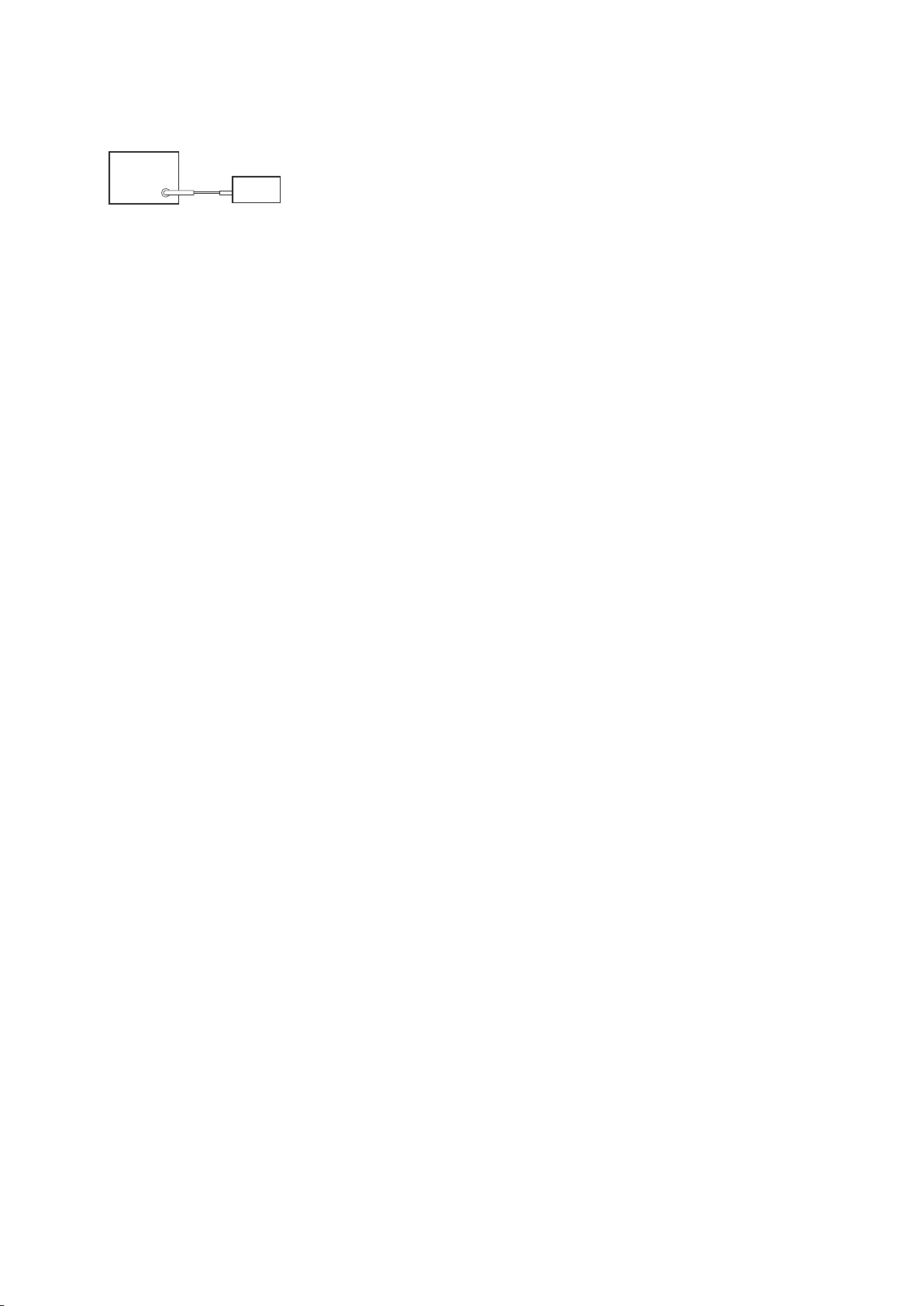
FM AUTO STOP CHECK
signal
generator
Procedure:
1. Turn on the set.
2. Input the following signal from signal generator to FM antenna
input directly.
Carrier frequency : A = 87.5 MHz, B = 98 MHz, C = 108 MHz
Deviation : 75 kHz
Modulation : 1 kHz
ANT input : 35 dBu (EMF)
Note: Use 75 ohm coaxial cable to connect signal generator and the set.
You cannot use video cable for checking.
Use signal generator whose output impedance is 75 ohm.
3. Set to FM tuner function and scan the input FM signal with
automatic scanning.
4. Confi rm that input frequency of A, B and C are detected and
automatic scanning stops.
set
STR-KS370
When the station signal is received in good condition, automatic
scanning stops.
9
STR-KS370
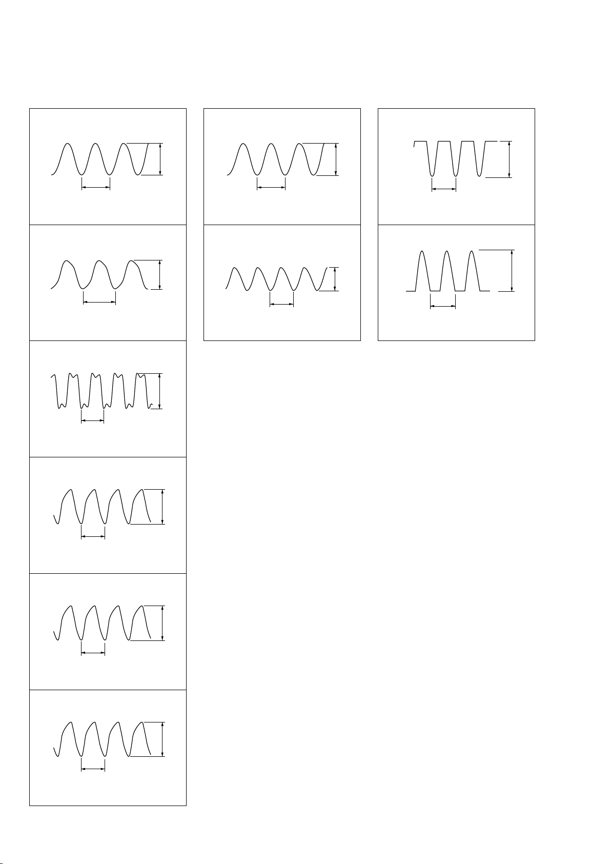
• Waveforms
SECTION 5
DIAGRAMS
– MAIN Board –
IC1003 <zvc (XTAL)
1
40 ns
500 mV/DIV, 20 ns/DIV
IC1005 qd (Xout)
2
200 ns
2 V/DIV, 100 ns/DIV
IC1704 wa (XOUT(O))
3
1.1 Vp-p
3.4 Vp-p
– HDMI PC Board – – DISPLAY Board –
IC3500 4 (XTALOUT)
7
100 ns
1 V/DIV, 50 ns/DIV
IC3000 qa (XOUT)
8
100 ns
2 V/DIV, 50 ns/DIV
3.2 Vp-p
3.5 Vp-p
Q701 (Base)
9
Q701 (Collector)
q;
6.2 Ps
1 V/DIV, 5 Ps/DIV
6.3 Ps
5 V/DIV, 5 Ps/DIV
3 Vp-p
15.8 Vp-p
81 ns
2 V/DIV, 50 ns/DIV
IC2004 4 (Y)
4
20.2 ns
1 V/DIV, 10 ns/DIV
IC2000 qf (XFSOOUT)
5
20.2 ns
1 V/DIV, 10 ns/DIV
IC2001 qf (XFSOOUT)
6
4 Vp-p
2.6 Vp-p
2.4 Vp-p
10
2.4 Vp-p
20.2 ns
1 V/DIV, 10 ns/DIV
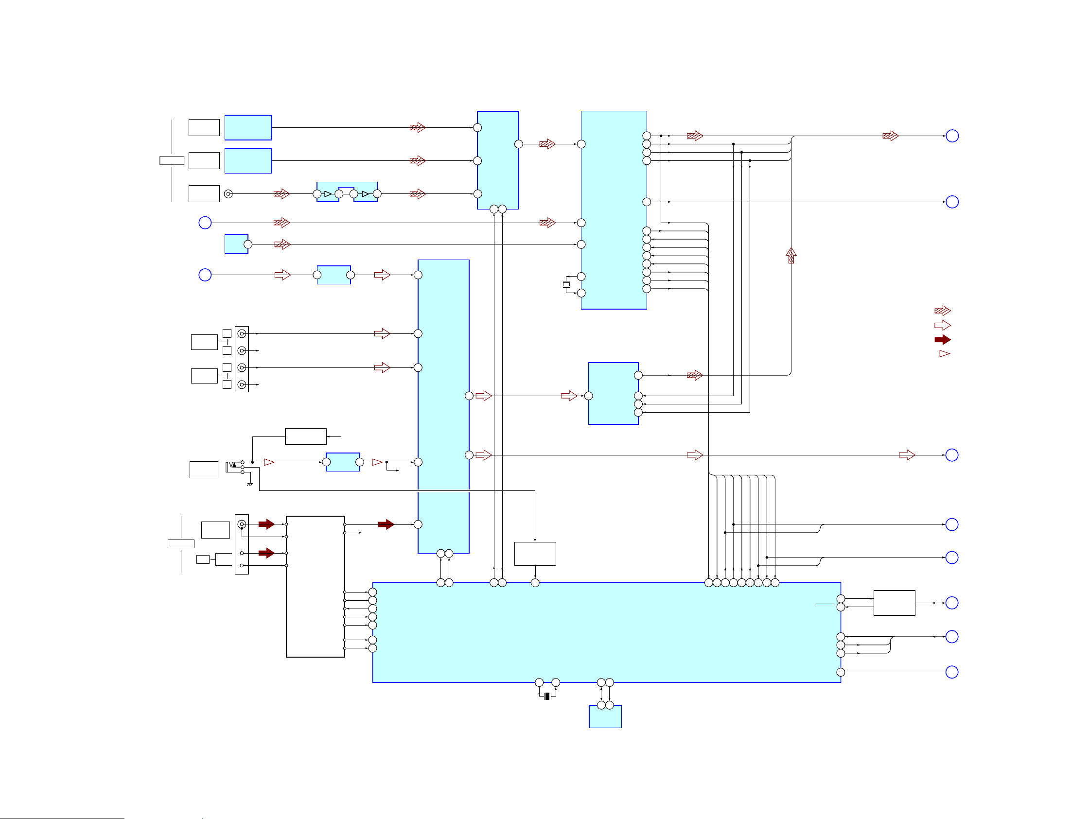
5-1. BLOCK DIAGRAM - MAIN Section -
STR-KS370
DIGITAL
(PAGE 12)
(PAGE 13)
ANTENNA
TV OPT IN
SAT/CATV
OPT IN
J202
VIDEO
COAX IN
J
N
TV AUDIO IN
SA-CD/CD
AUDIO IN
AUTO
CAL MIC
COAXIAL
AM
FM 75Ω
HDMISPDIF
IC3527
L
R
L
R
DIGITAL OPTICAL
RECEIVER
IC203
DIGITAL OPTICAL
RECEIVER
IC202
ARC_SPDIF
AMP
2
J201
J200
R-CH
R-CH
GAIN CONTROL
Q200
TUNER (FM/AM)
FM ANT
GND
AM ANT
GND
1
3
WAVE SHAPPER
IC211
7
LINE AMP
IC1705
MIC AMP
5
IC209
L CH
R CH
A+9V
DIGITAL AUDIO
INPUT SELECTOR
IC210
1C0
6
1Y
7
1C1
5
2
6
DMPORT L
DCAC R
9
TV L
5
SACD L
3
ANALOG AUDIO
INPUT SELECTOR
1
DCAC L
TUNER L
11
OUT L
IC212
SAIR OUT L
DATA23CLK
22
1
7
R-CH
IC2
4
A
2B14
X1700
12.288MHz
14
18
PLUG DETECT
SWITCH
Q201
DIGITAL AUDIO
INTERFACE RECEIVER
DIN0
3
DIN2
5
DIN1
4
XOUT(O)
21
22
XIN(I)
A/D CONVERTER
VinL
13
IC1704
IC1703
DATA(O)
CKOUT
BCK(O)
LRCK(O)
AUDIO(O)
XMODE
XSTATE(O)
ERROR(O)
CSFLAG(O)
DOUT
SCKI
BCK
LRCK
DATA_DIR, DOUT,
BCK, LRCK, CKOUT
AUDIO
SAIR OUT L
SC_SHIFT, SC_SCDT
DIR_XSTATE, DIR_RERR
(PAGE 13)
A
(PAGE 13)
B
x R-ch is omitted due to same as L-ch.
x SIGNAL PATH
: AUDIO (DIGITAL)
: AUDIO (ANALOG)
: TUNER
: MIC
(PAGE 13)
M
(PAGE 14)
P
(PAGE 13)
C
DIR_CE
DIR_RST
DIR_XSTATE
DATA_DIR
CKOUT
BCK
LRCK
DOUT
ERR
DIR_SCFLAG
SC_SHIFT
SC_SCDT
DIR_RERR
DIR_XSTATE
16
13
14
15
24
DIR_ZERO
DO
35
DI
36
CLK
38
CE
37
48
17
34
25
9
6
8
7
DIR_DO
DIR_DIN
DIR_CLK
DIR_CE
DIR_RST
DIR_XSTATE
ERR
DIR_CSFLAG
DIR_DO
DIR_ZERO
DIR_DIN
DIR_CLK
STR-KS370
DO/ST/SD
DI
CL
CE
TUNED_SD TUNED
RDS DATA
RDS CLK
43
45
41
40
44
42
75
ST_DI
ST_DO
ST_CLK
ST_CE
RDS_DATA
RDS CLK
86
87
BD3842DATA
BD3842CLK
51
66
TC74VHC153A
TC74VHC153B
11
DCACON/OFF
Xout
13 15
X1001
5MHz
18
100 1 2 24 2769 10
DIR_ZERO
DIR_HDOUT
SYSTEM CONTROLLER
IC1005 (1/4)
Xin
ROM_SDA
53
5 6
EEPROM
IC1014
ROM_SCLK
54
DAMP_SCDT/DIR_DIN
DAMP_SHIFT/DIR_CLK
DIR RST
DIR_HCE
DIR_XSTATE
19
DIR ERROR
DIR CSFLAG
CEC_DO
CEC_DI
UCOM RX-HDMI_TX
UCOM TX-HDMI_RX
HDMI_RST
HDMI_CNVSS
HRXD
HTXD
HRESET
CEC DATA
SWITCH
Q1006 – 1009
22
3
36
35
94
61
HRESET,
HTXD, HRXD
HDMI_CNVSS
CEC
D
(PAGE 12)
E
(PAGE 12)
U
(PAGE 12)
1111

STR-KS370
5-2. BLOCK DIAGRAM - HDMI PC Section -
&(&
D
(PAGE 11)
+'0,
&1
'9',1
&1
%',1
'$7$
'$7$±
'$7$
'$7$±
'$7$
'$7$±
&/2&.
&/2&.±
6'$9
6&/9
+273/8*'(7
932:(5
&(&
'$7$
'$7$±
'$7$
'$7$±
'$7$
'$7$±
&/2&.
&/2&.±
6'$9
6&/9
+273/8*'(7
932:(5
&(&
5;
7
9
4
6
1
3
12
16
15
19
18
13
7
9
4
6
1
3
12
16
15
19
18
13
121
123
122
125
124
119
118
36
35
34
33
129
132
131
134
133
128
127
39
38
37
5;
5;
5;
5;
5;
5;&
5;&
'6'$
'6&/
+3'
53:59
5;
5;
5;
5;
5;
5;
5;&
5;&
'6'$
'6&/
+3'
53:(59
+'0,
,1387
6(/(&725
,&
6'
6'
6'
6'
6&.
63',)
0&.
96<1&
+6<1&
2'&.
44
:6
DE
99
73
74
75
76
6&.
63',)
0&.
96<1&
+6<1&
2'&.
&1
&(&
13
7;
34
7;±
33
7;
37
7;±
'±'
±±
±
6'
6'
6'
6'
:6
DE
6'
6'
6'
6'
:6
6&.
63',)
0&.
DE
96<1&
+6<1&
2'&.
6'
9
17
'/2
8
6'
18
'5
6'
7
19
6
16
11
15
4
21
5
1
3
2
88
'/
6'
'5
:6
'5
6&.
'&/.
63',)
'/
0&/.
DE
96<1&
+6<1&
,'&.
+'0,
75$160,77(5
,&
36
7;
7;±
39
7;&
31
7;&±
'6'$
47
'6&/
46
+3'
51 19
5(6(7
&6'$
&6&/
6'
,17
24
25
49
48
6'
6'
6'
:6
6&.
63',)
0&.
3
4
%8))(5
5
6
7
8
2
9
,&
±
13
12
11
18
6'±6'
/5&.
%&.
0&.
+'0,B63',)
7
9
4
6
1
3
12
16
15
6'±6'0&.
%&./5&.
'$7$
'$7$±
'$7$
'$7$±
'$7$
'$7$±
&/2&.
&/2&.±
6'$9
6&/9
+273/8*'(7
)
(PAGE 13)
(PAGE 11)
J
79287
+'0,
&1
6$7&$79,1
(PAGE 15)
'$7$
'$7$±
'$7$
'$7$±
'$7$
'$7$±
&/2&.
&/2&.±
6'$9
6&/9
+273/8*'(7
932:(5
&(&
6,*1$/3$7+
7
9
4
6
1
3
12
16
15
19
18
13
Q
$8',2',*,7$/
+'0,
;
0+]
5;
139
5;
138
5;
141
5;
5;
143
5;
142
5;&
137
5;&
136
'6'$
44
'6&/
43
+3'
42
53:59 5(6(7
41
6%9&&
28
11
;287
13
;,1
;287
087(287
&6'$
&6&/
4
;
0+]
5
;,1
24
23
,17
22
21
27
&6&/
28
&6'$
+'0,&21752//(5
,&
19
5;567
5;,17
'
'
65
087(
42
43
7;B567
7;B,17
&1966
&,1985;
297
&287987;
5(6(7
%8))(5
,&
2
3
1
7
6
5
+5(6(7
+5;'
337;
+7;'
345;
417;B93:5
+'0,B&1966
'03257B7;
'03257B5;
&1
+5(6(7
+7;'+5;'
93:5
087(
3
&B287987;
5
&B,1985;
1
&1966
2
5(6(7
(PAGE 13)
G
(PAGE 11)
U
(PAGE 13)
5
(PAGE 11)
E
.
(PAGE 15)
1&
STR-KS370
1212
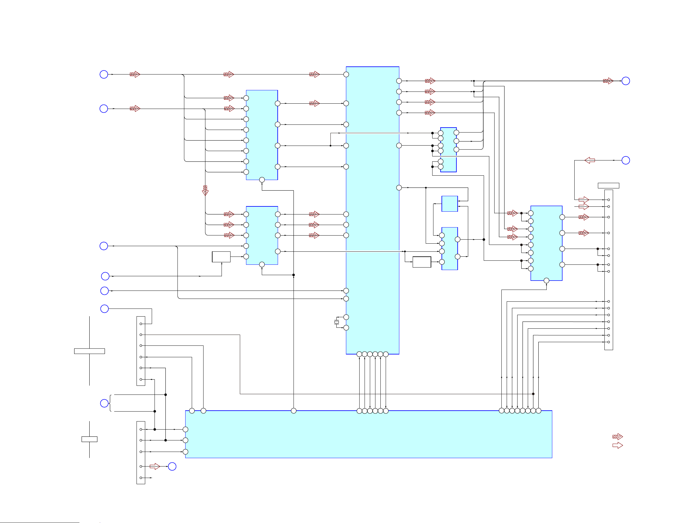
5-3. BLOCK DIAGRAM - DSP/S-AIR Section -
DATA_DIR, DOUT,
(PAGE 11)
(PAGE 12)
(PAGE 11)
(PAGE 12)
(PAGE 11)
(PAGE 15)
FLASH PROGRAMMING
BCK, LRCK CKOUT
A
SD0 – SD3, MCK,
F
C
G
B
S
BCK, LRCK
DIR_XSTATE, DIR_RERR
MUTE
AUDIO
CN1002
RESET
RTS1
CNVSS
CLK1
RXD1
TXD1
2
7
3
5
4
8
DATA_DIR
DOUT
LRCK
CKOUT
BCK
DIR_XSTATE
DIR_RERR
SD1
SD2
SD3
SD0
LRCK
MCK
BCK
MUTING
Q1700
SIGNAL SELECTOR
14 4A
13 4B
11 3A
10 3B
52A
62B
21A
31B
SWITCHING
31B
62B
10 3B
14
4A
13
4B
IC1701
SEL
1
IC1702
SEL
1
4Y 12
3Y 9
2Y 7
1Y 4
1Y 4
2Y 7
3Y 9
4Y 12
X1000
25MHz
78 DPSIA
79 DPSIB
88 DPLRCK
94 DPFSCK
89 DPLBCK
80 DPSIC
81 DPSID
82 DPSIE
97 NONAUDIO*
16 DIR_ERR
143
XTAL
142
CLKIN
125
SPICLK
127
MOSI
DSP
IC1003
126
MISO
SPIDS*
122
DPSOA 64
DPSOB 65
DPSOC 70
DPSOE 77
DPDVBCK 87
DPDVLRCK 86
INT_REQ
RESET*
15
121
MUTING
Q1004
BUFFER
14
13
2
3
5
6
SWITCHING
1
2
6
5
IC1015
SWITCH
IC1000
IC1002
12
4
7
7
3
AMP_DATA1
AMP_DATA2
AMP_DATA3
AMCK1
AMP_BCK1
AMP_LRCK1
2A0
3B0
5A1
6B1
11 A2
10 B2
14 A3
13 B3
BUFFER
IC1008
S
1
Y0 4
Y1 7
Y2 9
Y3 12
AMP_DATA1 – AMP_DATA3,
AMP_BCK1, AMP_LRCK1, AMCK
R-CH
S AIR OUT L
CN100
EZW-T100
4
2
16
26
15
24
14
23
19
18
7
12
25
20
11
STR-KS370
(PAGE 14)
H
(PAGE 11)
M
L ch
R ch
SD1
SD2
BCK1
BCK2
LRCK1
LRCK2
I2C_SDA
I2C_SCL
INT
ADC_SEL
GND
SRC_MUTE
RESN
STR-KS370
(PAGE 12)
DMPORT
DMPORT_TX
R
DMPORT_RX
DMPORT RX (UCOM TX)
DMPORT TX (UCOM RX)
DET
Rch
78
85
77
67
70
71
34
S-AIR GPIO2
SAIR_ADC_SEL
63
S-AIR RST
S-AIR_DET
S-AIR_SRC_MUTE
SIGNAL PATH
: AUDIO (DIGITAL)
: AUDIO (ANALOG)
33
9
CN1701
5
6
7
13
Lch
14
N
R-CH
CLK1
31
UCOM TX-DMP RX
32
UCOM RX-DMP TX
91
DMPORT_DET
(PAGE 11)
CNVSS
21
PCM_MULTI
7
SYSTEM CONTROLLER
6
5
DSP MISO
DSP MOSI
DSP_SPI CLK
IC1005 (2/4)
26
88
DSP SPIDS
68
DSP_INTR
DSP_RESET
SAIR_SEL
S-AIR_I2C_SDA
S-AIR_I2C_SCL
1313

STR-KS370
5-4. BLOCK DIAGRAM - AMP Section -
(PAGE 13)
(PAGE 11)
AMP_DATA1 – AMP_DATA3,
AMP_BCK1, AMP_LRCK1, AMCK1
H
SC_SHIFT,
SC_SCDT
P
SYSTEM CONTROLLER
IC1005 (3/4)
DAMP_LATCH1
DAMP_LATCH2
DAMP_LATCH3
DAMP_INIT
OVERFLOW1
OVERFLOW2
DAMP_SOFT_MUTE
DAMP_NSP_MUTE
DRIVE _RST(EN)
82
79
80
76
83
84
72
56
81
SC_SCDT
SC_SHIFT
SC_SCDT
SC_SHIFT
SC_SCDT
SC_SHIFT
AMP_DATA1
AMP_BCK1
AMP_LRCK1
AMCK1
AMP_DATA2
AMP_BCK1
AMP_LRCK1
AMCK1
AMP_DATA3
AMP_BCK1
AMP_LRCK1
AMCK1
SOFT_MUTE
NSP_MUTE
LAT1
LAT2
LAT3
INIT
OVF1
OVFW
LAT1
INIT
SOFT_MUTE
NSPMUTE
PGMUTE
LAT2
INIT
SOFT_MUTE
NSPMUTE
PGMUTE
LAT3
INIT
OVFW
OVF1
SOFT_MUTE
NSP_MUTE
PGMUTE
STREAM PROCESSOR
31 DATA1
30 BCK
29 LRCK
36 XFSIIN
21 SCDT
22 SCSHIFT
23 SCLATCH
27 INIT
24 OVF FLAGR
25
OVF FLAGL
19 SOFT MUTE
18 NSP MUTE
20 PGMUTE
STREAM PROCESSOR
31 DATA2
30 BCK
29 LRCK
36 XFSIIN
21 SCDT
22 SCSHIFT
23 SCLATCH
27 INIT
24 OVF FLAGR
25
OVF FLAGL
19 SOFT MUTE
18 NSPMUTE
20 PGMUTE
STREAM PROCESSOR
31 DATA3
30 BCK
29 LRCK
36 XFSIIN
21 SCDT
22 SCSHIFT
23 SCLATCH
27 INIT
24 OVF FLAGR
25 OVF FLAGL
19 SOFT MUTE
18 NSP MUTE
20 PGMUTE
IC2000
IC2001
IC2002
OUTL1(+) 11
OUTL2(–) 9
OUTR1(+) 6
OUTR2(–)
XFSOIN
XFSOOUT 14
FSOCKO
FSOI
OUTL1(+) 11
OUTL2(–)
OUTR1(+)
OUTR2(–)
XFSOIN
XFSOOUT 14
FSOI
OUTR1(+) 6
OUTR2(–)
OUTL1(+)
OUTL2(–)
XFSOIN
FSOI
DIGITAL POWER AMP
IC2005
PWM_A
6 39
PWM_B
8 36
/RESET
17
4
CLOCK
48
37
38
9
6
4
48
38
4
11
9
48
38
BUFFER
IC2004
X2000
49.152MHz
16
PWM_C OUT_C
PWM_D18
/RESET
7
/SD
5
6
PWM_A
8
PWM_B
/RESET
17
16
PWM_C OUT_C
PWM_D
18
/RESET
7
/SD
5
16
PWM_C
18
PWM_D
/RESET
17
6
PWM_A OUT_C
PWM_B
8
/RESET
7
/SD
5
OUT_A
OUT_B
OUT_D
DIGITAL POWER AMP
IC2006
OUT_A
OUT_B
OUT_D
DIGITAL POWER AMP
IC2007
OUT_A
OUT_B
OUT_D
RESET
Q2020 – 2021
31
28
39
36
31
28
39
36
31
28
+3.3V
L.P.F.
L.P.F.
L.P.F.
L.P.F.
L.P.F.
L.P.F.
L.P.F.
L.P.F.
L.P.F.
L.P.F.
L.P.F.
L.P.F.
OVER LOAD
DETECT
Q2005, 2006
OVER LOAD
DETECT
Q2003, 2004
OVER LOAD
DETECT
Q2007, 2008
OVER LOAD
DETECT
Q2013, 2014
OVER LOAD
DETECT
Q2009, 2010
OVER LOAD
DETECT
Q2011, 2012
TB2002
+
_
+
_
+
_
+
_
TB2001
+
_
+
_
FRONT L
FRONT R
SUR L
SPEAKERS
SUR R
CENTER
SUBWOOFER
STR-KS370
(PAGE 15)
DRIVE OPC (DIAG)
SD
L
DC_DET
20
46
PROTECT DETECT
Q2018 – 2019
DC DETECT
Q2017
+31.5V
SIGNAL PATH
: AUDIO (DIGITAL)
: AUDIO (ANALOG)
1414

5-5. BLOCK DIAGRAM - SMPS Section -
STR-KS370
(PAGE 14)
D380
DISPLAY
INDICATOR
D729
(G)
DISPLAY
INDICATOR
SD
L
FL700
FLUORESCENT
INDICATOR
TUBE
LED DRIVE
Q380
LED DRIVE
Q700
D729
(O)
ACTIVE
STANDBY
S350
INPUT
SELECTOR -
S351
SOUND
FIELD
S352
INPUT
SELECTOR +
S301
I/1
MASTER
VOLUME
FLUORESCENT
INDICATOR TUBE DRIVER
IC700
SEG17
14 – 29,31
SEG1 – SEG16,
42 – 31
GRID1 – GRID12
1
SW1
2
SW1
LED DRIVE
REMOTE CONTROL
RECEIVER
IC750
ROTARY
ENCODER
RV750
DIN
CLK
STB
Q702
+31.5V
RECT
REGULATOR
SHUNT
REGULATOR
IC951
D931
SHUNT
IC931
RECT
D941
RECT
D942
RECT
D943
ISOLATOR
PC903
ISOLATOR
PC901
T902
SUB POWER
TRANSFORMER
ISOLATOR
PC902
D1003
D932
7
8
9
60
FL_D_OUT
57
FL_CLK
59
FL_LAT
58
CEC_STBY_LED
95
AD KEY
74
POWER KEY
90
KEY_0
4
SIRCS_IN
92
VOL JOG
SYSTEM CONTROLLER
IC1005 (4/4)
23PCONT_2
39PCONT_3_SAIR
47P_CONT4_DSP
50PCONT_1
97P_CONT_HDMI
73AC_CUT
12RESET
FOR FLUORESCENT
INDICATOR TUBE
HDMI +3.3V
HDMI +1.8V
VEE
+1.8V
REGULATOR
IC3523
RESET
SWITCH
Q1005
POWER ON/OFF
CONTROL
Q943, 947
+5V
OSC
Q701
+1.8V
REGULATOR
IC3528
REGULATOR
IC1010
+5V
REGULATOR
IC1700
K
+5V
REGULATOR
IC1009
+9V
REGULATOR
IC1012
+2.5V
REGULATOR
IC1001
+3.3V
REGULATOR
IC943
5VPWR
D1008
D1007
D3515D3514
D1001D1002
POWER VOLTAGE
CONTROL
Q981, 982
+5V
REGULATOR
IC3510
+12V
REGULATOR
IC941
+5V
REGULATOR
IC942
Q
(PAGE 12)
B+ SWITCH
Q946
+6.4V
REGULATOR
IC3509
SAIR +4V
AVCC
HDMI +5V
(PAGE 12)
T700
DC/DC
CONVERTER
F1
F2
RECT
D726 – 727
AMP +12V
+5V
REGULATOR
IC1013
REGULATOR
IC2003
HDMI +1.8V
+1.8V
A +9V
DMPORT +5V
DSP +1.2V
AMP +1.8V
D +3.3V
+3.3V
REGULATOR
IC3526
STBY +3.3V
RESET SIGNAL
GENERATOR
IC1006
+5V
T901
MAIN POWER
TRANSFORMER
D905
D914, 915
D922
RECT
D901
B+ SWITCH
Q921
TH901
D908
D906, 907
D910
LF902
LINE
FILTER
B+ SWITCH
Q901
POWER CONTROL
1
D
4
VCC
6
FB/OLP
8
STARTUP
D909
IC921
LF901
LINE
FILTER
POWER CONTROL
IC901
3
D
4
VCC
1
OCP
5
OLP
F901
(AC IN)
STR-KS370
(PAGE 13)
S
1515
STR-KS370
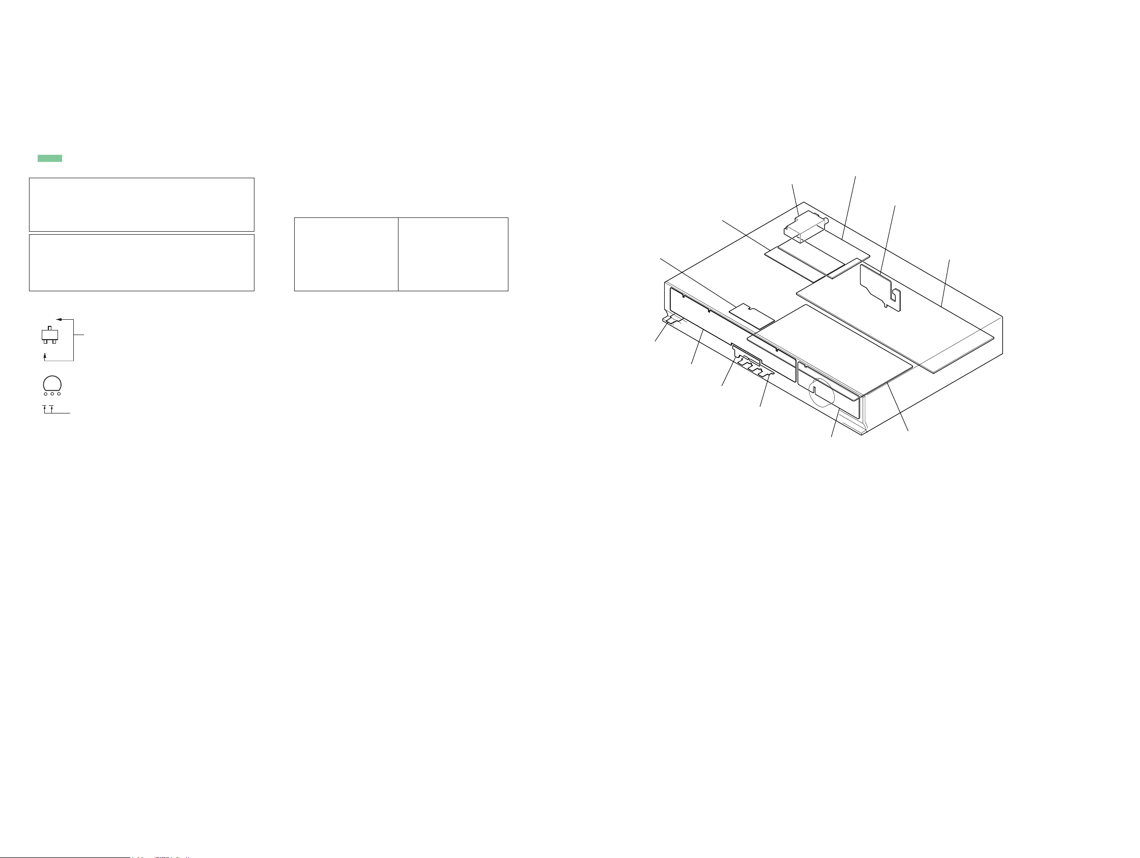
THIS NOTE IS COMMON FOR PRINTED WIRING BOARDS AND SCHEMATIC DIAGRAMS.
(In addition to this, the necessary note is printed in each block.)
For Printed Wiring Boards.
Note:
• X : Parts extracted from the component side.
• Y : Parts extracted from the conductor side.
• f : Internal component.
• : Pattern from the side which enables seeing.
(The other layers' patterns are not indicated.)
Caution:
Pattern face side:
(Conductor Side)
Parts face side:
(Component Side)
Caution:
Pattern face side:
(SIDE B)
Parts face side:
(SIDE A)
• Indication of transistor.
C
Q
B
E
CEB
These are omitted.
Parts on the pattern face side seen
from the pattern face are indicated.
Parts on the parts face side seen from
the parts face are indicated.
Parts on the pattern face side seen
from the pattern face are indicated.
Parts on the parts face side seen from
the parts face are indicated.
These are omitted.
For Schematic Diagrams.
Note:
• All capacitors are in μF unless otherwise noted. (p: pF) 50
WV or less are not indicated except for electrolytics and
tantalums.
• All resistors are in Ω and 1/4 W or less unless otherwise
specifi ed.
• f : internal component.
• 2 : nonfl ammable resistor.
• 5 : fusible resistor.
• C : panel designation.
Note:
The components identifi ed by mark 0 or dotted
line with mark 0 are critical for safety.
Replace only with part
number specifi ed.
• A : B+ Line.
• B : B– Line.
• Voltages and waveforms are dc with respect to ground
under no-signal (detuned) conditions.
no mark : TUNER
* : Impossible to measure
• Voltages are taken with VOM (Input impedance 10 M).
Voltage variations may be noted due to normal production
tolerances.
• Waveforms are taken with a oscilloscope.
Voltage variations may be noted due to normal production
tolerances.
• Circled numbers refer to waveforms.
• Signal path.
J : AUDIO (DIGITAL)
F : AUDIO (ANALOG)
f : TUNER
E : HDMI
N : MIC
Note:
Les composants identifi és
par une marque 0 sont
critiques pour la sécurité.
Ne les remplacer que par
une piéce portant le numéro spécifi é.
• Circuit Boards Location
HDMI PC board
FFC SUPPORT board
KEY FUNCTION board
DISPLAY board
LED board
KEY SELECTOR board
TUNER (FM/AM)
IR board
IO board
S-AIR board
MAIN board
SMPS board
STR-KS370
1616
STR-KS370
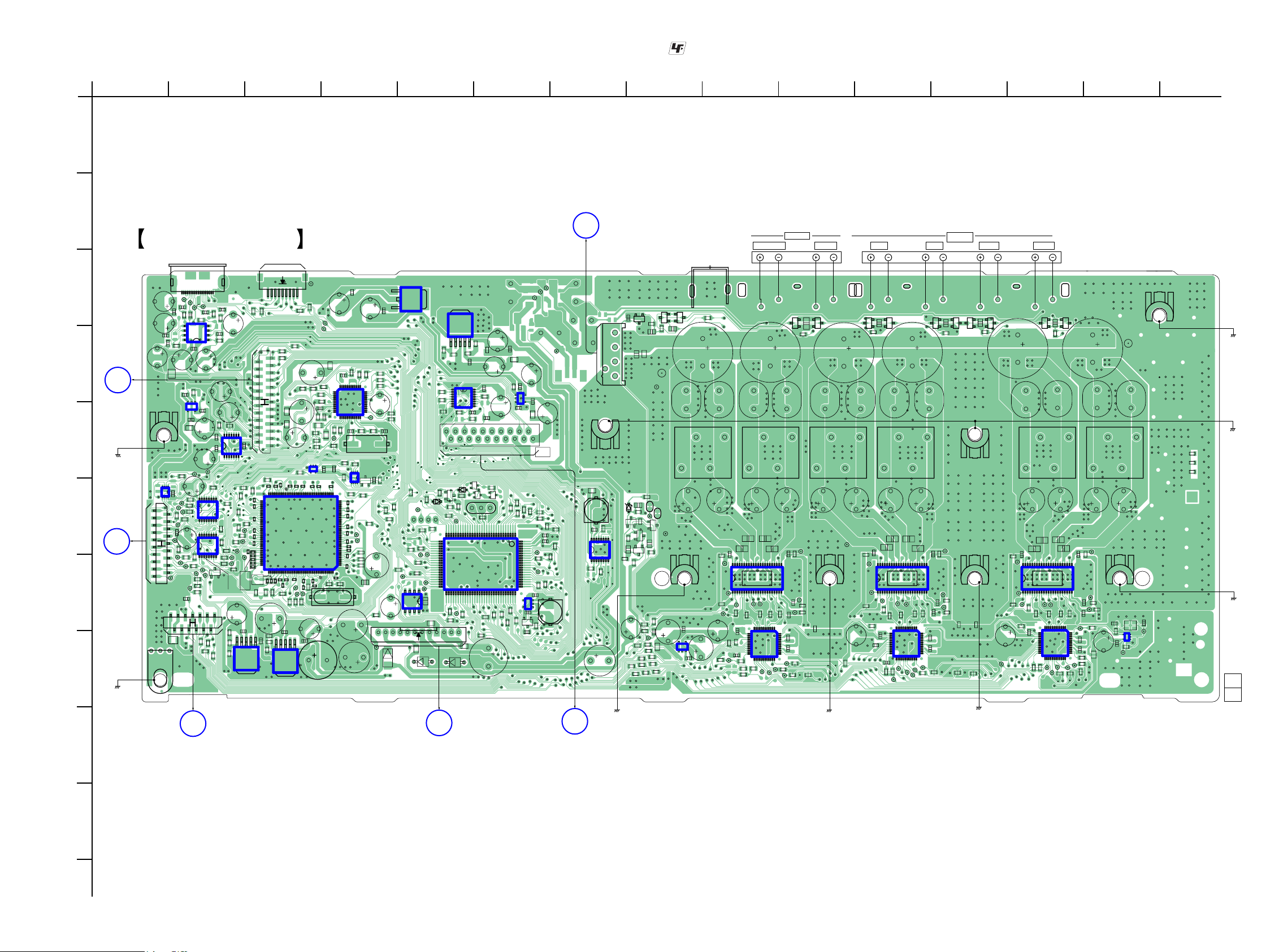
5-6. PRINTED WIRING BOARD - MAIN Board (Component Side) -
1 2 3 4 5 6 7 8 9 10 11 14 1512 13
A
B
MAIN BOARD (COMPONENT SIDE)
FLASH PROGRAMMING
C1509
R1725
R1729
R1730
R1724
C1701
R1741
C1729
R1031
C1062
R1125
R1130
C1055
JL1035
IC1014
C1300
R1309
JL1006
IC1012
IO
R1720
R1721
R1036
R1126
CL1010
R1094
R1083
R1086
JL1026
JL1025
R1301
R1047
R1136
JL1033
JL1029
1
4
5
8
L1003
CNP100
FB2002
D1008
SMPS BOARD
CN906
(PAGE 31)
C
D
IO BOARD
(PAGE 24)
E
F
HDMI PC
G
(PAGE 26)
H
I
C
CNS200
(CHASSIS)
F
BOARD
CN3512
(CHASSIS)
CN1701
CL1711
CL1701
C1759
C1722
C1705
C1724
IC1700
IC1011
1
19
CN1007
EB1001
C1756
2
18
13
L1701
EB1700
L1000
CL1032
CL1027
12
R1740
C1520
R1335
C1523
CL1033
C1742
C1723
R1340
R1119
CL1057
C1760
R1743
CL1031
CL1030
C1736
CL1000
CL1029
C1718
R1118
CL1034
C1091
C1708
FB1708
R1113
R1114
R1115
584
C1706
CL1036
C1762
R1116
R1090
CL1041
CL1042
R1082
R1095
R1089
CNS700
CL1702
C1741
R1117
R1733
C1703
C1751
C1748
IC1701
16
CL1039
R1140
A
DISPLAY BOARD
CNS701
(PAGE 29)
118
CL1703
C1740
C1743
R1742
R1745
C1700
R1744
C1755
1
R1739
IC1705
C1726
C1744
C1745
R1750
C1749
C1747
IC1703
CL1028
R1713
R1706
916
1
8
R1703
R1701
R1700
9
L1010
CL1051
R1702
8
1
CL1053
R1705
R1704
BE
R1737
Q1700
CL1040
IC1702
1
2
R1141
R1310
R1139
R1142
R1318
IC1009
C1311
R1751
CL1055
R1313
R1024
R1023
CL1054
R1707
R1033
C1312
CL1049
C1030
C1507
C1028
C1027
C1024
C1750
L1011
CL1050
C1506
6
R1154
C1040
C1033
R1223
C1309
15
C1013
R1004
R1153
CNS201
C1042
C1037
C1034
C1032
C1508
C1014
24
2
R1025
R1006
C1047
C1003
R1000
19
CN1002
R1155
R1129
R1128
25
R1131
R1306
C1719
FB1710
FB1707
C1752
1
R1034
C1048
C1049
C1050
C1505
72
73
IC1003
108
109
C1015
C1017
C1016
C1012
R1011
CL1047
R1007
R1009
R1008
C1002
R1002
C1001
15
R1003
6
IC1001
CL1012
R1156
CL1002
CL1004
IC1704
FB1700
C1761
R1723
R1726
R1753
R1738
R1731
C1717
C1707
FB1702
R1718
R1716
CL1043
R1715
FB1701
R1732
R1717
IC1000
C1060
C1061
C1053
C1051
C1052
R1012
C1010
C1018
C1011
C1019
X1000
R1013
R1010
C1000
C1310
C1252
C1738
48
1
12
13 24
R1722
R1030
C1054
37
36
1
144
C1020
R1032
C1036
R1005
C1730
C1039
C1035
C1504
C1029
R1026
C1081
C1038
C1512
C1043
R1029
C1031
C1503
C1025
R1727
R1019
R1017
C1082
C1083
R1728
37
36
25
JL1076
R1734
X1700
IC1002
BE
Q1004
R1027
R1022
CL1037
CL1048
R1021
C1046
• See page 16 for Circuit Boards Location.
SMPS BOARD
CN904
(PAGE 31)
G
JL2002
JL2087
C1255
L1009
R1185
C1250
C1113
Q1009
R1064
R1158
R1071
C1080
R1157
R1222
IC1006
JL2001
C1525
C1111
IC1013
C1112
L1008
19
R1060
R1147
R1148
R1050
R1049
R1055
JL1010
C1067
C1065
JL1024
R1096
JL1031
R1134
C1085
R1105
BE
Q1005
C1078
TP2001
C1524
FB1002
R1076
R1073
R1135
C1251
R1097
R1112
C1519
R1332
IC1015
B
S-AIR BOARD
CN104
(PAGE 24)
EB1000
C1518
16
18
C1513
IC1010
6
15
R1044
R1045
IC1008
R1051
1
R1042
8
R1061
R1065
1
220
D1005
Q1006
R1099
BE
R1106
D1003
R1133
R1138
R1098
JL1021
R1093
R1190
R1304
C1254
R1191
R1192
C1256
C1257
C1092
16
R1074
9
C1106
C1510
CN110
R1305
BE
R1108
Q1008
B
B
E
E
Q1007
X1001
R1067
IC1005
C1301
R1143
JL1032
R1165
R1336
R1145
112
L1007
D1001D1002
C1088
R1188
R1163
E
9
R1330
4
CN2002
R1325
• : Uses unleaded solder.
TB2001
SPEAKERS
CENTERSUBWOOFER
B2000
Q2017
C2196
C2033
1
C2204
R2147
D2126
TP2007
Q2018
BE
R2151
C2205
Q2020
R2148
R2150
R2152
C2345
R1181
TP2003
R1182
R1175
R1180
R1178
R1176
R1173
BE
BE
BE
R1172
R2140
C2197
R2155
CL2008
JL2098
R2146
R2149
Q2021
R1321
R1338
Q2009
Q2010
BE
BE
C2073
R2141
SL2001
SL2002
BE
Q2019
CL2004
C2206
IC2003
R2145
C2341
C2046
FB2000
R1174
R1179
R1177
R2099
C2297
L2012 L2013
JL2122
TP2005
C2307
R2038
R2040
R2041
C2342
44
1
JL2126
C2328
R2205
R2039
C2026
C2331
R2018
JL2133
R2019
C2260
R2128
12
13
24
25
C2283 C2284
C2293
IC2007
R2209
EB2000
C2035
C2034
C2036
JL2128
C2023
JL2125
R2210
R2020
C2325
JL2135
TP2014
C2278
R2129
C2327
1
36
TP2030
48
37
C2319
23
22
JL2141
C2316
JL2138
R2100
R2101
C2303
C2031
IC2002
C2030
TP2033
R2159
R2022
TP2032
TP2031
Q2012
BE
R2113
R2202
JL2142
R2198
R2023
R2200
R2021
C2072
BE
Q2011
C2287C2288 C2289 C2290
EB2005
R2028
Q2007
C2298
C2294
IC2006
CL2007
R2208
JL2123
JL2124
R2211
C2013
R2009
R2036
BE
R2085
C2306
C2017
44
1
JL2127
C2071
R2204
C2016
C2043
C2329
C2259
R2013
Q2008
BE
C2265C2266 C2267C2268
C2330
JL2132
R2087
R2014
TP2010
TP2009
C2279
C2272C2273
C2324
C2326
JL2134
R2072
R2088
12
1
13
48
24
37
25
36
TP2026
TP2024
R2158
TP2025
(CHASSIS)(CHASSIS)
TB2002
SPEAKERS
SUR RSUR L FRONT RFRONT L
C2070
Q2013
Q2005
Q2014
BE
BE
BE
R2127
EB2003
R2203
23
R2073
C2318
22
C2317
C2302
C2021
C2020
TP2027
R2017
JL2143
JL2140
R2201
JL2139
R2199
R2026
IC2001
R2016
R2015
EB2004
R2024
(CHASSIS)
Q2006
B
E
C2069
R2069
IC2005
IC2000
TP2008
R2187
JL2092
JL2093
R2178
C2003
C2255
C2247 C2249
C2242
C2323
C2322
C2243
44
1
JL2096
JL2630
R2164
R2034
R2057
C2006
R2007
L2003L2006L2007
13
TP2011
TP2012
R2008
BE
R2058
12
24
25
Q2003
C2068
C2320
JL2670
C2253
TP2013
R2011
R2055
C2321
R2042
1
48
37
36
R2010
BE
R2043
23
22
R2228
TP2015
TP2002
Q2004
TP2016
C2263
C2010
C2270
C2251
R2185
JL2102
C2011
R2012
R2157
C2240
C2231
JL2101
R2033
FB2003
C2234 C2235
L2000
C2238
EB2001
JL2103
R2184
R2183
C2040
X2000
R2035
C2038
C2039
JL2003
CL2003
C2207
JL2055
IC2004
R2031
EB2002
JR
JR
JR
1-881-001-
(CHASSIS)
(CHASSIS)
(CHASSIS)
11
(11)
J
STR-KS370
1717

STR-KS370
5-7. PRINTED WIRING BOARD - MAIN Board (Conductor Side) -
1 2 3 4 5 6 7 8 9 10 11 14 1512 13
A
MAIN BOARD (CONDUCTOR SIDE)
B
C
D
E
F
G
TP2000
C2237
C2236
JL2091
JL2090
C2337
R2160R2161
JL2052
C2012
C2239
R2054
JL2089
C2008
JL2051
JL2088
C2066
C2232
C2233
C2220
JL2097
R2224
C2248
C2004
JL2100
C2009
TP2019
R2053
C2254
C2230
R2177
R2165
C2007
C2005
C2250
C2044
TP2020
C2221
C2067
C2252
C2241
C2335
R2166
C2218
R2068
C2256
TP2004
JL2053
C2047
C2091
JL2078
R2067
JL2095
TP2021
C2244
JL2094
C2246
TP2022
C2219
C2092
C2045
C2216
C2154
R2126
TP2035
TP2036
JL2048
JL2047
JL2110
JR
JR1005
• See page 16 for Circuit Boards Location.
CL2002
TP2037
C2155
C2217
TP2038
C2175
C2215
R2125
JL2049
C2333
C2271
C2269
C2276
C2262
JL2105
JL2118
C2301
C2018
JL2107
R2188
C2296
C2014
C2019
C2264
C2257
R2206
C2015
JL2109
R2191 R2192
R2227
C2022
R2084
C2282
C2292
C2291
C2309
C2214
JL2050
JL2120
JL2117
R2194
R2083
C2176
C2336
C2211
C2156
JL2112
JL2115
TP2040
R2112
TP2039
JL2046
C2285
C2286
C2157
JR1004
JL2045
TP2041
C2212
C2210
C2208
R2111
C2339
C2223
JL2111
JL2104
C2224
JL2108
JL2106
R2189
R2190
JL2119
C2275
R2226
C2299
C2032
C2024
C2028
JR
C2029
C2295
C2258
TP2042
C2025
C2027
C2226
C2225
R2098
R2207
• : Uses unleaded solder.
C2213
C2209
R2097
JL2076
JL2077
C2338
C2281
C2222
C2227
TP2006
JL2121
JL2116
R2195
C2308
C2037
R2193
JL2113
JL2114
C2348
C2229
C2228
CL2005
C2343
CL2009
CL2010
C1514
JR1010
C1716
CL1071
JR
C1007
CL1017
CL1715
CL1018
CL1707
CL1725
CL1721
CL1717
CL1020
JR1008
JR1013
JR
JL1007
CL1021
CL1730
CL1710
C1058
JR
JR1007
CL1022
CL1705
CL1723
JR
CL1073
CL1023
CL1724
CL1718
CL1713
CL1024
CL1706
CL1727
CL1709
CL1720
CL1729
JR1011
CL1708
CL1722
CL1716
C1021
CL1025
CL1712
JR
CL1728
CL1726
C1266
JR1009
CL1006
CL1075
JR1012
JR
R1719
CL1035
FB1703
FB1704
C1521
C1702
R1747
R1746
R1735
R1736
CL1714
D1700
C1746
D1701
R1137
CL1052
CL1056
JR
CL1026
R1341
CL1074
CL1016
CL1015
CL1003
FB1705
FB1706
C1714
C1522
CL1007
CL1001
JR
JR1001
CL1072
C1709
C1710
C1715
C1711
JL1019
R1164
C1071
R1075
R1171
R1028
R1059
JL1018
JL1015
R1052
R1063
R1169
R1066
R1103
C1075
R1068
JL1027
R1168
C1073
R1187
R1160
C1089
R1035
R1167
JL1013
R1087
R1166
R1111
C1105
R1109
JL1016
R1170
R1159
R1069
C1074
FB1001
JL1017
R1102
CL1070
R1110
R1070
C1066
CL1069
C1103
CL1008
L1004
CL1005
R1146
JL1011
R1092
CL1068
C1258
CL1066
JR1002
R1100
CL1064
CL1065
JR
R1077
R1078
C1259
CL1067
R1053
CL1063
CL1062
C1093
CL1061
L1005
CL1060
R1014
CL1059
R1084
R1085
JR1006
C1072
C1712
JR
C1005
JR1003
C1004
C1086
FB1013
JL1020
JL1012
JL1014
R1048
JR
JR1000
JR
C1261
D1000
CL1014
R1104
CL1013
R1101
CL1009
R1225
R1224
R1339
R1107
R1058
C1076
R1162
C1079
11
1-881-001-
(11)
H
I
J
STR-KS370
1818
STR-KS370
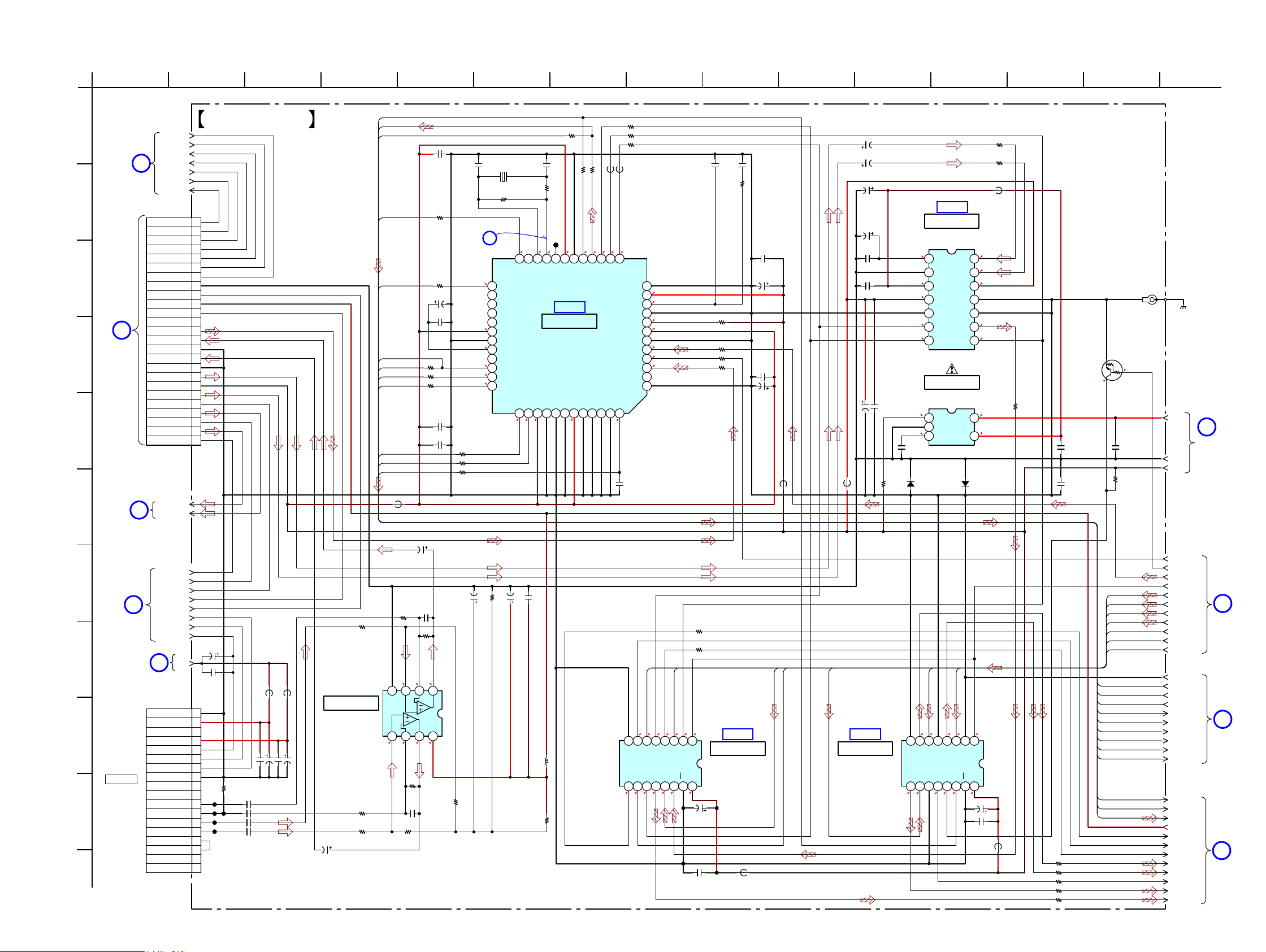
5-8. SCHEMATIC DIAGRAM - MAIN Board (1/5) -
1 2 3 4 5 6 7 8 9 10 11 14 1512 13
A
B
C
D
E
MAIN
BOARD
(3/5)
(Page 21)
A
IO
BOARD
CNS200
(Page 25)
8
ST_TUNED
ST_CLK
RDS_CLK
RDS-DATA
RDS DATA
RDS CLK
DO/ST/SD
TUNED SD
TC74VHC153 B
TC74VHC153 A
TUNER GND
OPT OUT
DMPORT L
DMPORT R
ANALOG OUT R
ANALOG OUT L
BD3842 DATA
SAIR OUT R
BD3842 CLK
SAIR OUT L
DCAC ON/OFF
MAIN BOARD (1/5)
ST-CE
ST_DI
SD-DO
CNS201
25P
25
24
23
22
CL
21
DI
20
CE
19
18
AGND
17
16
+9AV
15
14
13
12
11
DGND
10
9
DGND
8
7
+3.3V
6
5
4
3
2
1
• See page 10 for Waveforms. • See page 33 for IC Block Diagrams. • See page 38 for IC Pin Function Description.
DIR_XSTATE
DATA_DIR
DIR_ZERO
DIR_NONAU
DIR_CSFLAG
DIR_RERR
DIR_ERR
DIR_DO
DIR_DIN
DIR_CE
DIR_CLK
DIR_RST
R1730
R1729
R1732
1k
C1712
C1729
0.1
33p
12.288MHz
R1721
100
3
R1720
100
C1701
16V47
C1715
0.1
0R1724
100
100
C1711
0.1
C1709
0.1
R1725
R1727
3.3
25
26
27
28
29
3.3
30
31
1.8
32
33
3.3
34
3.3
35
0
36
0
0R1728
0
C1730
X1700
33p
R1734
1k
R1741
1M
JL1076
XIN(I)
EMPHA
AUDIO(O)
CSFLAG(O)
F0(O)
F1(O)
F2(O)
FV(O)
DVDD
DGND
VREF
BPSYNC(O)
ERROR(O)
DO
DI
CE
CL(I)
37 38 39 40 41 42 43 44 45 46 47 48
0 0 3.3 3.3 3.3
DVDD
XOUT(O)
XMCK(O)
IC B/D
IC1704
DIGITAL AUDIO
INTERFACE RECEIVER
IC1704
LC890561W
XSEL(I)
MODE0(I)
MODE1(I)
DGND
DGND
DVDD
100
R1722
100
R1718
XSTATE(O)
DOSEL0(I)
DATA(O)
LRCK(O)
DOSEL1(I)
CKSEL0(I)
FB1701
131415161718192021222324
BCK(O)
SPDIF(O)
CKSEL1(I)
1.71.71.72.53.33.31.61.60
CKOUT
LPF(O)
DISEL(I)
XMODE
C1738
FB1702
AGND
AVDD
AGND
AD_IN
DVDD
DGND
DIN2
DIN1
DIN0
0.01
100R1717
220R1716
330R1715
C1707
C1717
0.1
0.022
R1731
220
C1716
0.1
C1719
470
C1710
C1761
10V
0.1
470
10V
FB1710
12
3.3
11
0
10
9
3.3
8
3.3
7
6
0.3
5
2.8
4
0
3
2
1
R1738 10k
R1753
R1726
100
100
100R1723
FB1707
C1751
C1748
C1747
C1744
1
50V
C1745
1
50V
10
50V
10
50V
0.1
C1749
0.1
50V
10
C1752
C1750
0.1
R1733
1k
IC B/D
IC1703
A/D CONVERTER
IC1703
PCM1808PWR
2.5
1
Vref
VinR
2
AGND
3
AVcc
4
DVdd
5
DGND
6
SCKI
LRCK BCK
IC1700
+5V REGULATOR
IC1700
TK11150CSCL-G
1
CTRL
2
GND
CNp Vout
D1700
VinL
FMT
MOD1
MOD0
DOUT
Vin
5
3.4
1.7
1.7 1.7
1.3
3.3
C1736
1000p
MA2J1110GLS0
2.5
14
2.5
13
3.4
12
11
10
1.3
9
87
5
5
6.3
43
D1701
MA2J1110GLS0
R1750
R1751
FB1708
100
100
EB1700
E
(CHASSIS)
Q1700
RT1N141C-TP-1
MUTING
3.1
0
R1713
100
E+6V
3
AGND
+3.3V
MAIN
BOARD
(2/5)
(Page 20)
C1708
C1746
1000p
1
C1703
R1737
1
10k
F
G
H
I
J
STR-KS370
BOARD
(Page 21)
DMPORT
DC5V
0.7A MAX
14
MAIN
BOARD
(3/5)
(Page 21)
11
MAIN
(3/5)
SAIR-OUT-L
SAIR-OUT-R
DCACON/OFF
BD3842CLK
BD3842DATA
TC74VHC153A
TC74VHC153B
DMPORT_DET
DMPORT_TX
DMPORT_RX
5
MAIN
BOARD
(2/5)
(Page 20)
VBUS(5V)
VIDEO5V
DMPORT RX (UCOM TX)
DMPORT TX (UCOM RX)
WM DET
WM A/D
(Lch)AGND
(Rch)AGND
WM RX
WM TX
DGND
DGND
VIDEO
VGND
FB1700
C1726
10
50V
HDMI_SD0
C1755
100p
R1744
22k
R1745
IC1705
LINE AMP
IC1705
NJM4565M(TE2)
R1742
R1743
22k
22k
22k
4321
V-
5 5 5 8
R1746
47k
R1740
C1512
1000
6.3V
+5V
C1086
0.1
FB1704
C1705
0.1
C1722
C1740 1
C1743 1
C1741
C1742 1
FB1703
C1760
0.1
C1759
100
100
16V
16V
1
C1724
10
50V
CN1701
18P
1
2
3
NC
4
5
6
DET
7
8
R1719
9
100
10
CL1703
11
CL1702
12
CL1701
Lch
13
CL1711
Rch
14
15
16
17
18
C1756
100p
C1700
R1739
47k
505
V+
8765
47k
R1747
47k
C1723
R1736
47 0.1
16V
100
4.7k
16V
C1706
L1701
R1735
3.3k
100R1701
220R1700
HDMI_SD2
2Y
3B3A4Y4B4A
HDMI_SD1
00001.701.71.701.7
1A1B1Y2A2B
SEL
ST
VDD
161514131211109
3.40.30.2000
C1718
10
50V
C1702
0.1
FB1706
R1703
HDMI_BCK
HDMI_MCK
0 0
87654321
1A
1B
1Y
2A
2B
2Y
10uH
GND3Y
3B3A4Y4B4A
1.7 0 1.7 1.3 0 1.3 3.4
ST
161514131211109
IC B/D IC B/D
IC1701
SEL
SIGNAL SELECTOR
IC1701
TC74VHC157FT(EKJ)
VDD
C1762
10
50V
C1714
0.1
FB1705
HDMI_SD0
HDMI_LRCK
HDMI_SD3
IC1702
SWITCHING
IC1702
TC74VHC157FT(EKJ)
87654321
GND3Y
HDMI_SD1
HDMI_SD2
HDMI_SD3
HDMI_LRCK
HDMI_BCK
HDMI_MCK
DIR_CLK
DIR_CE
DIR_DIN
DIR_DO
DIR_ERR
DIR_CSFLAG
DIR_RST
DIR_XSTATE
DIR_ZERO
DIR_RERR
DIR_NONAU
DATA_DIR
100R1704
100R1705
100R1707
100
100R1706
ARC_SPDIF
HDMI_MUTE
HDMISPDIF
MULTI_PCM
HDMI_SD0
HDMI_SD1
HDMI_SD2
HDMI_SD3
HDMI_LRCK
HDMI_BCK
HDMI_MCK
DGND
DIR_CLK
DIR_CE
DIR_DIN
DIR_DO
DIR_ERR
DIR_CSFLAG
DIR_RST
DIR_XSTATE
DIR_ZERO
DIR_RERR
DIR_NONAU
DATA_DIR
A+9V
LRCK
MCK
BCK
SI_D
SI_C
EMG_MUTE
SI_E
SI_B
9
MAIN
BOARD
(3/5)
(Page 21)
10
MAIN
BOARD
(3/5)
(Page 21)
1
MAIN
BOARD
(2/5)
(Page 20)
1919
 Loading...