

Sony RM-X63E, XVM-75V, XT-991V Service Manual
SERVICE MANUAL
• XTL-75V is composed of the following models.
• The TV Tuner unit (XT-991V) attached to the XTL-75V is same model as XTL-750W.
For further description, see the Service Manual of XTL-750W (9-925-662-
[][]
).
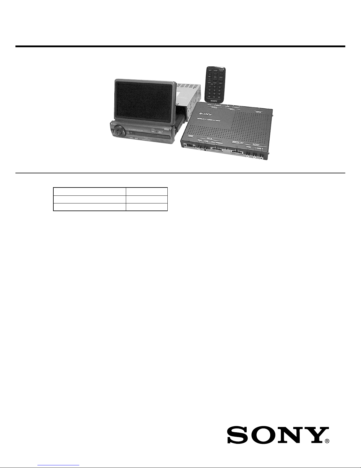
MOBILE COLOR TV
Chinese Model
SPECIFICATIONS
XTL-75V
TV Monitor XVM-75V
TV Tuner unit XT-991V
Wireless remote commander RM-X63E
TV Tuner unit: XT-991V
TV Monitor: XVM-75V
Wireless remote commander:
RM-X63E
TV Monitor (XVM-75V)
System Liquid crystal color display
Display Transparent TN LCD panel
Drive system TFT active matrix system
Picture size 6.5 in.; 142.6 × 80.8 mm,
165 mm
(w × h, diagonally)
Picture segment
336,960 (w 1440 × h 234)
Speaker type 35 × 20 mm dynamic speaker × 1
Power requirements
12 V DC car battery
(negative ground)
Current drain Approx. 1.0 A
Dimensions 178 × 50 × 180.7 mm (w × h × d)
Operating temperature
5˚C ~ +45˚C
Mass Approx. 2 kg
TV Tuner unit (XT-991V)
Television system
CCIR I,D,K system
Color system TV: PAL
Video: PAL, NTSC
Channel converge
VHF:1 CH ~ 12 CH
UHF: 21 CH ~ 69 CH
Power requirements
12 V DC car battery
(negative ground)
Current drain Approx. 0.5 A
Output terminals
Video output: RCA pin 1 Vp-p,
75 ohm
Audio output: RCA pin –10 dBs,
10 kohm
Monitor output: Square 16 -pin
(exclusive)
Input terminals Video input (2 system): RCA pin 1 Vp-p,
75 ohm
Audio input: RCA pin –10 dBs, 10 kohm
Antenna input: mini plug
Navigation input:Square 16 -pin
(exclusive)
RCA pin:
Video 1 Vp-p, 75 ohm
Audio (monaural)
–10 dBs, 10 kohm
Dimensions 202 × 30 × 140 mm (w × h × d)
Mass Approx. 750 g
Wireless remote commander (RM-X63E)
Power requirements
AA (R6) battery × 2
Operable rangeApprox. 3 m
Dimensions 62 × 25 × 115 mm (w × h × d)
Mass Approx. 100 g
(including batteries)
Supplied accessories
Wireless remote commander
RM-X63E (1)
Design and specifications are subject to change
without notice.

2
(XT-991V)
TABLE OF CONTENTS
1. SERVICING NOTES............................................... 2
2. DISASSEMBLY ......................................................... 4
3. ASSEMBLY ................................................................. 9
4. TEST MODE.............................................................. 10
5. ELECTRICAL ADJUSTMENTS......................... 11
6. DIAGRAMS
6-1. Block Diagram
– AUDIO/VIDEO/MODE CONTROL Section – .......... 15
6-2. Block Diagram
– SENSOR/MOTOR/POWER SUPPLY Section –........ 16
6-3. Note for Printed Wiring Boards
and Schematic Diagrams ................................................ 17
6-4. Pr inted Wiring Board – B Board – ................................ 18
6-5. Schematic Diagram – B Board – ................................... 19
6-6. Printed Wiring Board – A Board (Side A) –.................. 20
6-7. Printed Wiring Board – A Board (Side B) –.................. 21
6-8. Schematic Diagram – A Board (1/3) – .......................... 22
6-9. Schematic Diagram – A Board (2/3) – .......................... 23
6-10. Schematic Diagram – A Board (3/3) – .......................... 24
6-11. Printed Wiring Boards
– SENSOR/MOTOR Section –....................................... 25
6-12. Schematic Diagram – SENSOR/MOTOR Section – .... 25
6-13. Printed Wiring Board – G Board – ................................ 26
6-14. Schematic Diagram – G Board – ................................... 27
6-15. Printed Wiring Board – PANEL Board – ...................... 28
6-16. Schematic Dia gram – PANEL Board – ......................... 29
6-17. IC Pin Function Description ........................................... 34
7. EXPLODED VIEWS................................................ 36
8. ELECTRICAL PARTS LIST ............................... 40
Notes on chip component replacement
• Never reuse a disconnected chip component.
• Notice that the minus side of a tantalum capacitor may be dam-
aged by heat.
SECTION 1
SERVICING NOTES
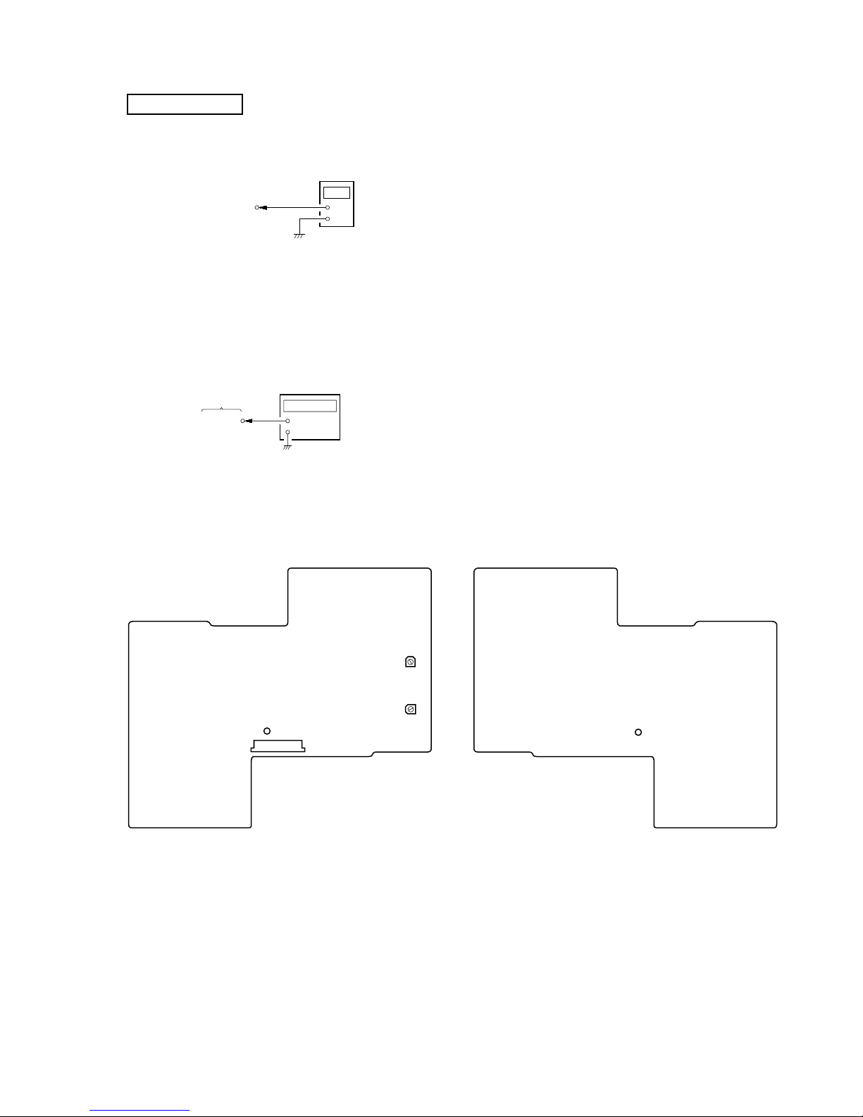
PRECAUTION ON REPLACING THE B BOARD
The R999 necessary for this set is not mounted on the B board for
repair. Also, the R711 unnecessary for this set is mounted.
Therefore, when replacing the B board, add R999 and remove R711
by referring to the following.
– SCHEMATIC DIAGRAM –
R999 0
R711
0
#
#
– PRINTED BOARD –
%
^
Loaction: G-11
3
two screws
four screws
three screws
screw
monitor gear (L)
g
ear (slide L)
slider knob (L)
slider knob (L)
2
1
3
front panel section
slider knob (R)
shaft
(stopper)
monitor
slider knob (R)
gear (slide R
)
monitor gear (R)
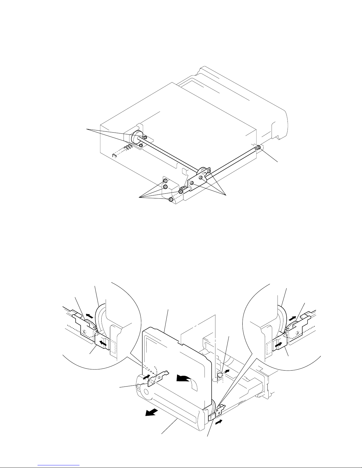
PRECAUTION ON HANDLING THE SET
During the manufacturing of this set, the slide gear phase has been
finely adjusted.
Therefore, never remove those screws shown in the figure when
making repairs.
HOW TO PULL UP THE MONITOR BY HANDS AT POWER OFF
1. Draw out the front panel fully in the direction of the arrow 1,
and remove the shaft (stopper) from the monitor.
2. Push the slider knob (L) and slider (R) in the direction of arrow 2.
(Meshing of gear (slide L) – monitor gear (L), and gear (slide
R) – monitor gear (R) can be disengaged)
3. Pull up the monitor in the direction of arrow 3.
4
SET
FRONT PANEL SECTION
(PAGE 4)
C BOARD
(PAGE 8)
MONITOR
(PAGE 8)
DC MOTOR (SMALL TYPE)
(ANGLE) (M11)
(PAGE 8)
COVER
(PAGE 6)
COVER
(PAGE 6)
HOW TO PULL UP THE MONITOR
(PAGE 6)
HOW TO PULL UP THE MONITOR
(PAGE 6)
B BOARD
(PAGE 5)
A BOARD
(PAGE 7)
D BOARD, DC MOTOR (SMALL TYPE)
(SLIDE) (M21)
(PAGE 7)
FRONT FRAME, CHASSIS (UPPER)
(PAGE 5)
FRONT PANEL SECTION
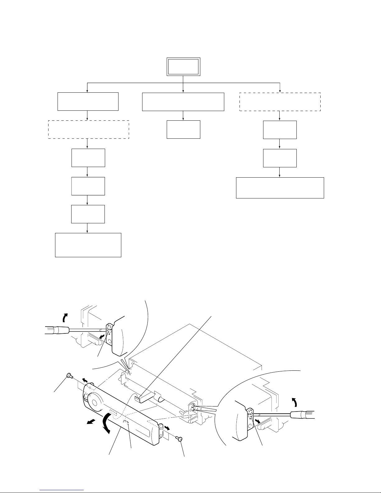
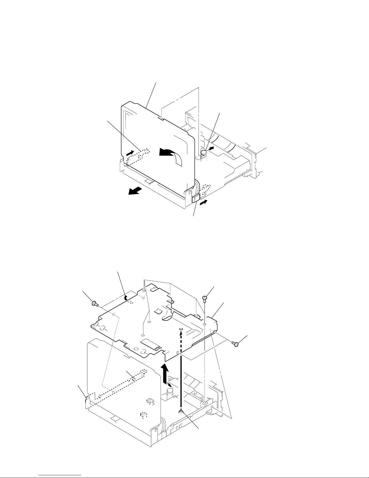
SECTION 2
DISASSEMBLY
Note: Follow the disassembly procedure in the numerical order given.
3 boss
2 two screws
(M2 × 3)
1
A
5 claw
4 Remove the front panel section
in the direction of arrow A.
2 two screws
(M2 × 3)
3 boss
6 flat cable 26P
(CN701)
• This set can be disassembled in the order shown below.
Note: Be sure to read the SERVICE NOTES before starting repairs.
5
FRONT FRAME, CHASSIS (UPPER)
B BOARD
1 screw
(B2.6 × 4)
4 front frame
Note: Do not pull the front
frame by force,
or it gets damaged.
1 screw
(B2.6 × 4)
5 boss
1 screw
(B2.6 × 4)
2 car mount bracket
1 screw
(B2.6 × 4)
1 screw
(B2.6 × 4)
6 chassis (upper)
1 screw
(B2.6 × 4)
3 five claws
1 screw
(B2.6 × 4)
2 car mount
bracket
5 boss
1 Pull the front panel ass’y.
2 four screws
(B2.6 × 4)
2 screw
(B2.6 × 4
)
4 binding
band
5 connection cords
(CN701, 702, 703)
6 B board
3 two flat cables (L) 26P
(CN705, 706)
Note: When removing the flat
cable (L) 26P, pull out
the front panel
but do not raise the B board
by force.
6
COVER
HOW TO PULL UP THE MONITOR
3 After making sure the shaft (stopper)
has been removed from the monitor,
pull up the monitor in the direction of arrow C.
shaft (stopper)
C
B
A
B
2 Push the slider knob (R)
in the direction of arrow B.
1 Pull the monitor base ass’y
in the direction of arrow A.
2 Push the slider knob (L)
in the direction of arrow B.
1 two screws
(M2 × 3)
2 Open this side, as there are screws
that fix the side plate.
1 six screws
(M2 × 3)
3 Remove the cover in the
direction of arrow A.
1 two screws
(M2 × 3)
A
S102
Note: When removing or
mounting the cover,
take care not to allow the cover
to be stuck to the S102.
screw head
side plate
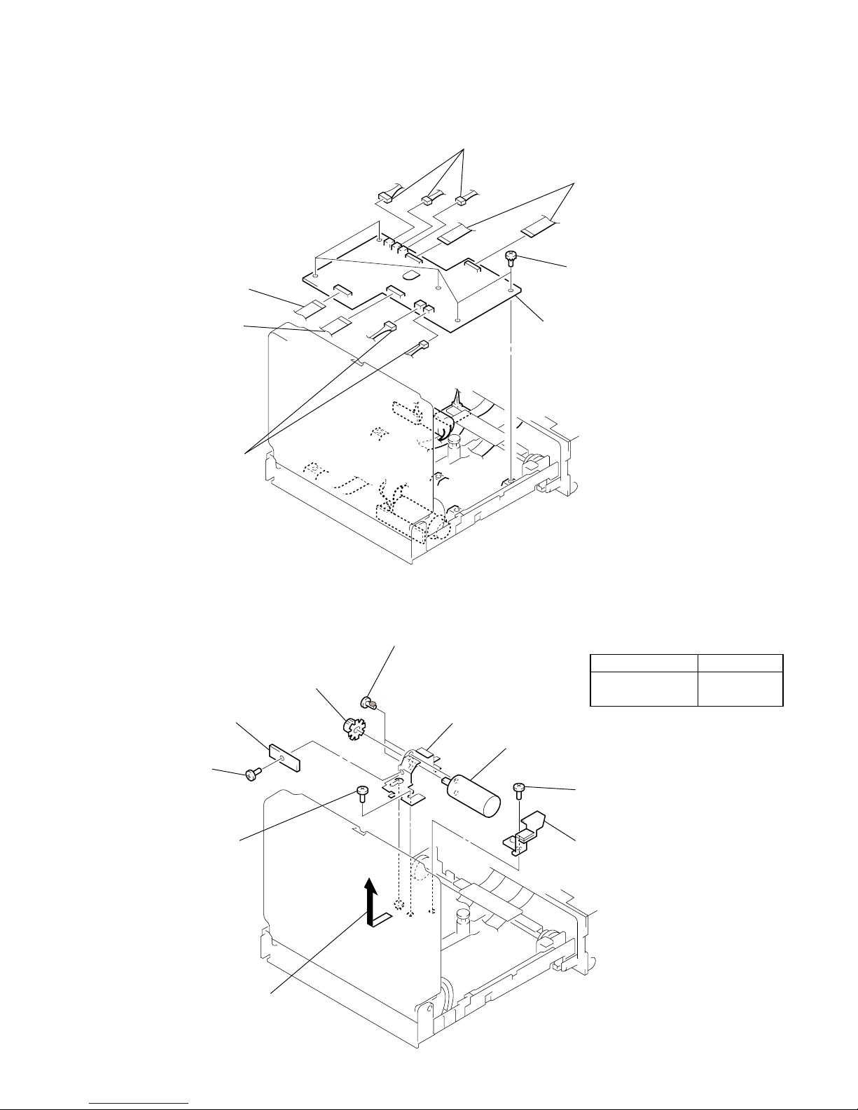
7
A BOARD
D BOARD, DC MOTOR (SMALL TYPE) (SLIDE) (M21)
2 three connectors
(CN104, 105, 107)
1 two flat cables (L) 26P
(CN101, 102)
3 five screws
(M2 × 4)
4 A board
1 flat cable 26P
(CN109)
1 flat cable 26P
(CN401)
2 two connectors
(CN106, 108)
8 two screws
(M2 × 3)
Note: When installing these screws
and DC motor, apply a drop
of screw lock G (1401B).
0 bracket (monitor motor)
9 DC motor (small type)
(slide) (M21)
1 screw (M2 × 3)
2 bracket (monitor stopper
)
5 screw
(M2 × 3)
6 D board
7 motor gear (slide)
3 screw
(M2 × 3)
4 Remove the bracket
(monitor motor) in the
direction of the arrow.
Part Name Part No.
SCREW LOCK G
7-432-114-11
(1401B)
8
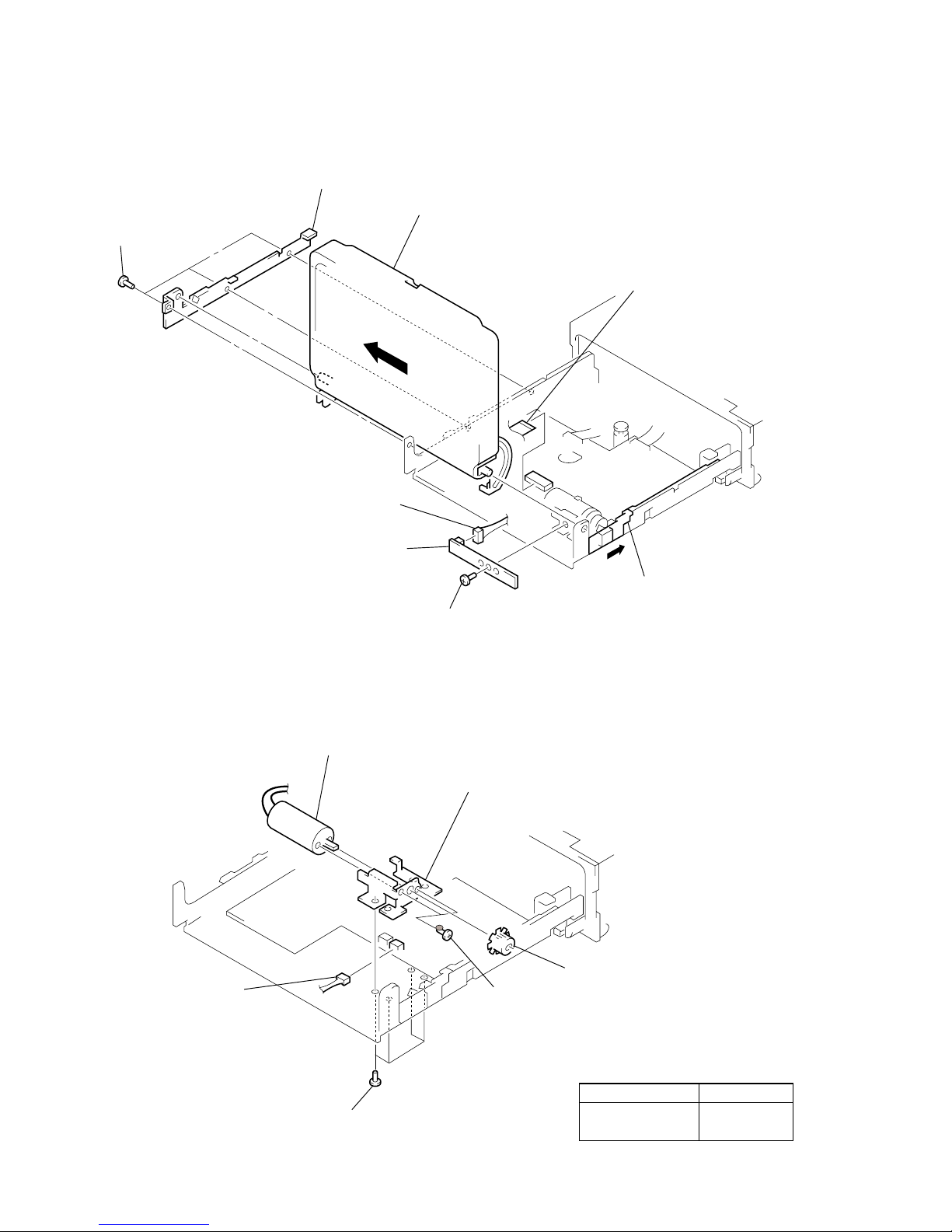
DC MOTOR (SMALL TYPE) (ANGLE) (M11)
C BOARD, MONITOR
5 three screws
(M2 × 3)
6 side plate
B
8 Remove the monitor in the
direction of arrow B.
1 flat cable 26P
(CN401)
A
7 Push the slider knob (R)
in the direction of arrow A.
4 C board
3 screw (M2 × 3)
2 connector
(CN11)
2 four screws
(M2 × 3)
1 connector
(CN108)
4 two screws
(M2 × 3)
3 motor gear (monitor)
6 bracket
(monitor motor)
5 DC motor (small type)
(angle) (M11)
B
Note: When installing these screw
s
and DC motor, apply a drop
of screw lock G (1401B).
Part Name Part No.
SCREW LOCK G
7-432-114-11
(1401B)
9
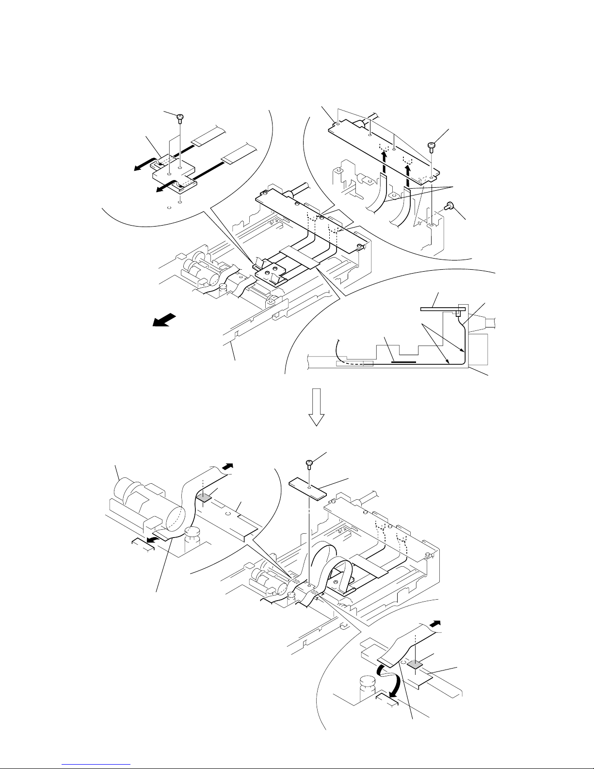
INSTALLATION OF FLAT CABLE (L) 26P
Note: Follow the assembly procedure in the numerical order given.
SECTION 3
ASSEMBLY
7 two screws
(M2 × 3)
6 FFC cover (2)
5
5
3 B board
4 four screws
(B2.6 × 4)
2 two flat cables (L) 26P
(CN705, 706)
4 screw
(B2.6 × 4)
B board
two flat cables (L) 26P
chassis (lower)
ass’y
Note: No slack is allowed.
filament tape 16 × 50
8 Using a filament tape 16 × 50,
stick two flat cables (L) 26P
to the chassis bottom without a slack
as shown in the figfure.
base ass’y
1 Pull the base ass’y
in the direction of arrow A.
A
0 Pull the flat cable (L) 26P in the direction of arrow B,
and stick it to the sheet (FFC) with an adhesive tape.
DC motor (small type) (slide) (M21)
B
adhesive tape
sheet (FFC)
qs screw (M2 × 3)
qa FFC cover (1)
0 Pull the flat cable (L) 26P
in the direction of arrow C,
and stick it to the sheet (FFC)
with an adhesive tape.
C
adhesive tape
sheet (FFC)
9 flat cable (L) 26P
(CN101)
9 Let the flat cable (L) 26P through
under DC motor (small type) (slide) (M21)
as shown in the figure, and connect to
the connector (CN102).

10
SECTION 4
TEST MODE
Test mode setting
1. Press the [OPEN/CLOSE] button to place the set in open state.
2. Press the [V ADJ] button and [TV/VIDEO] button simultaneously.
3. A beep sounds and the test mode is activated.
Note: The test mode is active for several seconds only, and it returns to
normal state if no operation is performed during this time. When
the test mode is activated, perform the following operation immediately.
Monitor position initializing
Return the position and angle at the time of monitor open state to
the initial position set in the factory.
1. Immediately after the Test mode is activated, press the
[SEARCH --] button and [TV/VIDEO] button. (A beep will
sound)
2. Press the RESET button, and the monitor is stored and the
monitor position is initialized. (Normal state will get back)
11
SECTION 5
ELECTRICAL ADJUSTMENTS
MAIN SECTION
5.35 V Adjustment
Connection:
Adjustment Procedure:
1. Connect a digital voltmeter to the TP1 (5.35 V) on the A board.
2. Adjust RV501 on the A board so that dig ital voltmeter reading
is 5.35 V.
Inverter Standard Frequency Adjustment
Connection:
Adjustment Procedure:
1. Connect a frequency counter to the CL299 on the A board.
2. Adjust RV502 on the A board so that frequency counter reading is 115 ± 2 kHz.
Adjustment Location:
digital voltmeter
A board
TP1 (5.35 V)
+
–
RV501
5.35 V
Adjustment
RV502
INVERTER
STANDARD
FREQUENCY
Adjustment
TP1 (5.35 V)
CN401
– A BOARD (Side A) –
A board
CL299
+
–
frequency counter
CL299
– A BOARD (Side B) –
12
MONITOR SECTION
Equipment Used
The measuring equipment below are used for these electrical
adjustments:
• Oscilloscope
• NTSC pattern generator
• PAL pattern generator
• Regulated DC power supply
• Digital voltmeter
Connection of Equipment
Unless otherwise specified, the measuring equipment should be
connected as shown below:
Setup at Adjustment
1. Press the
[SEL] button of the wireless remote commander, set
the image quality of the set to “VISUAL STD”.
2. The adjustment signal is a 5-step gray scale signal from a NTSC
pattern generator.
Input the gray scale signal into the tuner unit and connect an
oscilloscope to TP415 on the G board. Check that the width
between the black and white levels of the gray scale signal is
0.74 Vp-w.
Bright Adjustment
Adjustment Procedure:
1. Display the gray scale on the monitor screen.
2. Connect a digital voltmeter to TP (BRIGHT) on the G board.
3. Adjust RV405 so that the reading on the digital voltmeter is
2 V.
Adjustment Location: See page 13.
ACC cor
d
TV tuner unit
XT-991V
NTSC pattern
generator
MONITOR
OUT jack
INPUT (1)
(VIDEO)
jack
TV monitor
XVM-75V
regulated DC
power supply
(DC 14.4 V)
ACC cord
Connection
cord
parking brake terminal
(Connected to ground)
VIDEO OUT
(75 Ω)
+
–
white
black
0.74 Vp-p
V COM Amplitude/Bias Adjustment
Adjustment Procedure:
1. Display the gray scale on the monitor screen.
2. Connect an oscilloscope to TP (COM) on the G board.
3. V COM Amplitude Adjustment
Adjust R V401 so that the amplitude of the output wav eform is
6.0 V.
4. V COM Bias Adjustment
Adjust R V409 so that the lev el A of the output waveform is a t
4.3 V DC.
Adjustment Location: See page 13.
RGB Amplitude Adjustment
Adjustment Procedure:
1. Display the gray scale on the monitor screen.
2. Connect a oscilloscope to TP (G) on the G board.
3. Adjust RV406 so that the white and the next step of pedestal
are on the same level.
Adjustment Location: See page 13.
γ 0 Adjustment
Adjustment Procedure:
1. Display the gray scale on the monitor screen.
2. Connect an oscilloscope to TP (G) on the G board.
3. Adjust RV407 so that the third step from the bottom becomes
1.2 V.
Adjustment Location: See page 13.
6.0 Vp-p
0 V
A
pedestal
pedestal
white
white
1.2 V
GND

13
γ 2 Adjustment
Adjustment Procedure:
1. Display the gray scale on the monitor screen.
2. Connect a oscilloscope to TP (G) on the G board.
3. Adjust RV408 so that the white level becomes 3.6 V.
R Sub Bright Adjustment
Adjustment Procedure:
1. Display the gray scale on the monitor screen.
2. Connect a oscilloscope to TP (R) on the G board.
3. Adjust RV403 so that the third step from the bottom becomes
1.2 V.
Adjsutment Location:
3.6 V
GND
1.2 V
GND
B Sub Bright Adjustment
Adjustment Procedure:
1. Display the gray scale on the monitor screen.
2. Connect a oscilloscope to TP (B) on the G board.
3. Adjust RV404 so that the third step from the bottom becomes
1.2 V.
Note:
After all adjustments finished, enter connect the PAL pattern generator to
check that a picture appears.
1.2 V
GND
RV401
V COM
AMPLITUDE
Adjustment
RV404
B SUB
BRIGHT
Adjustment
RV406
RGB
AMPLITUDE
Adjustment
RV409
V COM BIAS
Adjustment
RV403
R SUB BRIGHT
Adjustment
RV405
BRIGHT
Adjustment
RV407
γ 0
Adjustment
RV408
γ 2
Adjustment
– G BOARD (Side A) –
TP (BRIGHT)
C424
TP (R)
TP (COM)
TP (G)
TP (B)
– G BOARD (Side B) –
TP415

14
MEMO
 Loading...