

Page 1
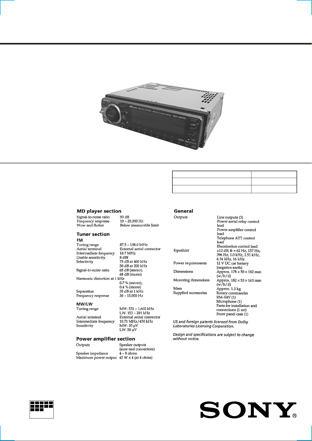
MDX-C8970R
SERVICE MANUAL
SPECIFICATIONS
AEP Model
UK Model
Model Name Using Similar Mechanism MDX-C7970R
Base Mechanism Type MG-164NF-138
Optical Pick-Up Name KMS-241B/J1NP
MICROFILM
FM/MW/LW MINIDISC PLAYER
Page 2

TABLE OF CONTENTS
1. SERVICE NOTE ....................................................... 3
2. GENERAL
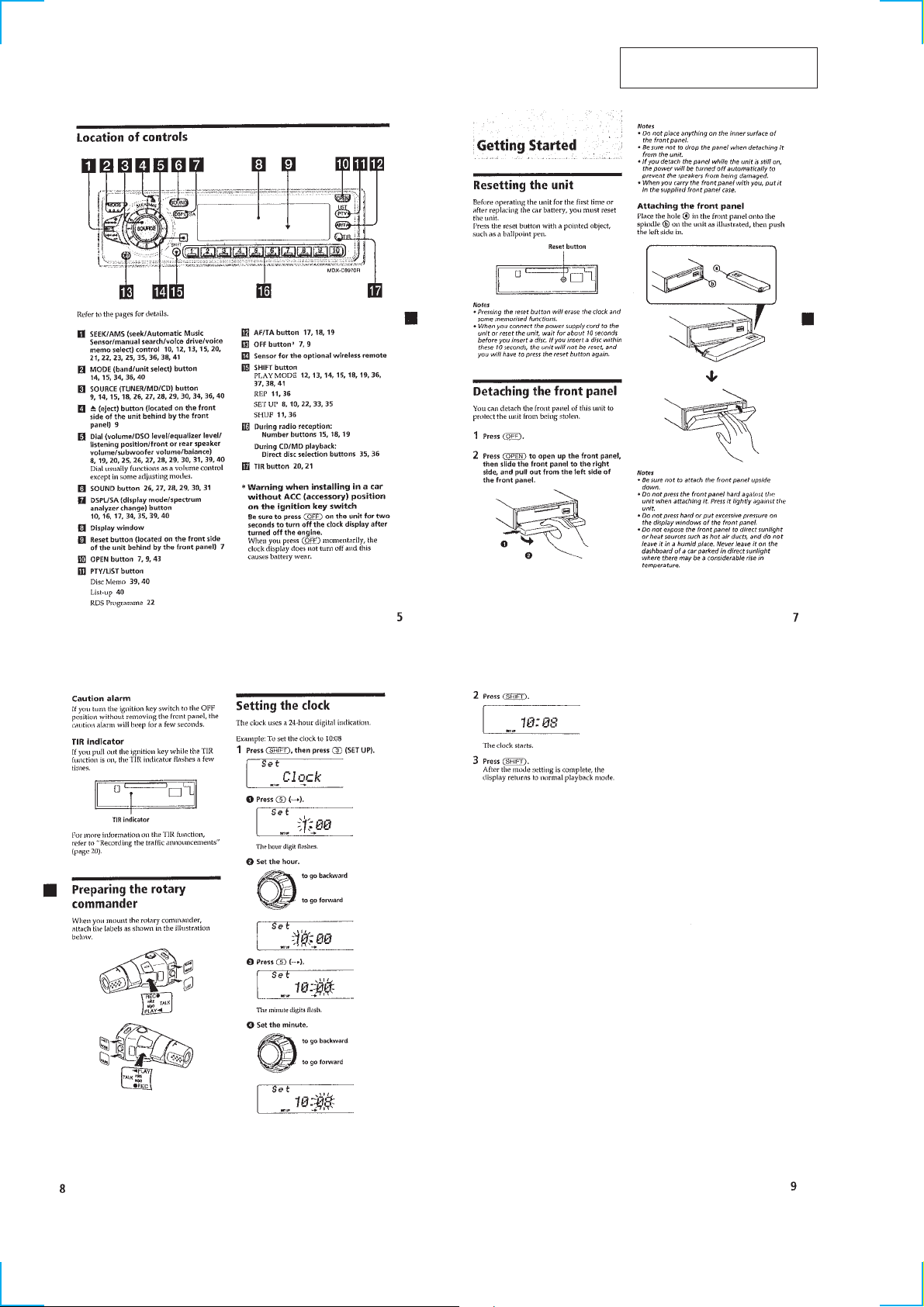
Location of controls ........................................................ 4
Resetting the unit ............................................................ 4
Detaching the front panel................................................ 4
Preparing the rotary commander .................................... 4
Setting the clock.............................................................. 4
Installation....................................................................... 5
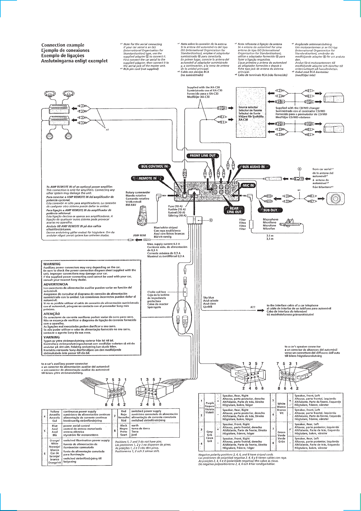
Connections ..................................................................... 6
Installation for microphone and rotary commander....... 9
3. DISASSEMBLY ......................................................... 11
4. ELECTRICAL ADJUSTMENTS
Test Mode........................................................................ 17
MD Section ..................................................................... 17
Tuner Section .................................................................. 17
5. DIAGRAMS
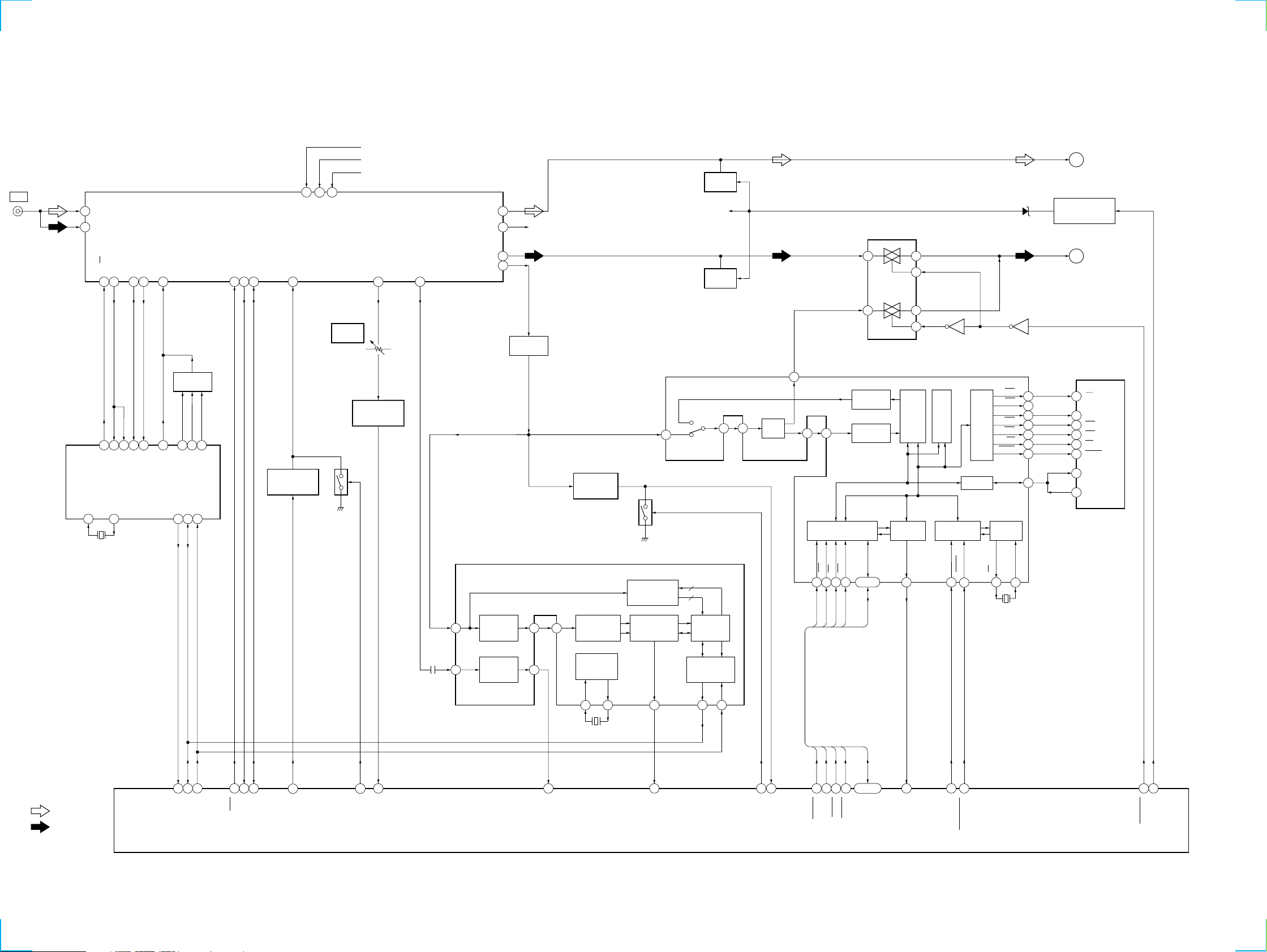
5-1. Block Diagram – SERVO Section – .............................. 21
5-2. Block Diagram – TUNER Section – ............................. 22
5-3. Block Diagram – MAIN Section – ................................ 23
5-4. Block Diagram
– DISPLAY/KEY CONTROL Section –........................ 24
5-5. Block Diagram
– BUS CONTROL/POWER SUPPLY Section –........... 25
5-6. Note for Printed Wiring Boards and
Schematic Diagrams ....................................................... 26
5-7. Printed Wiring Board – SERVO/SENSOR Boards –.... 27
5-8. Schematic Diagram
– SERVO (1/2)/SENSOR Boards – ............................... 28
5-9. Schematic Diagram – SERVO Board (2/2) – ................ 29
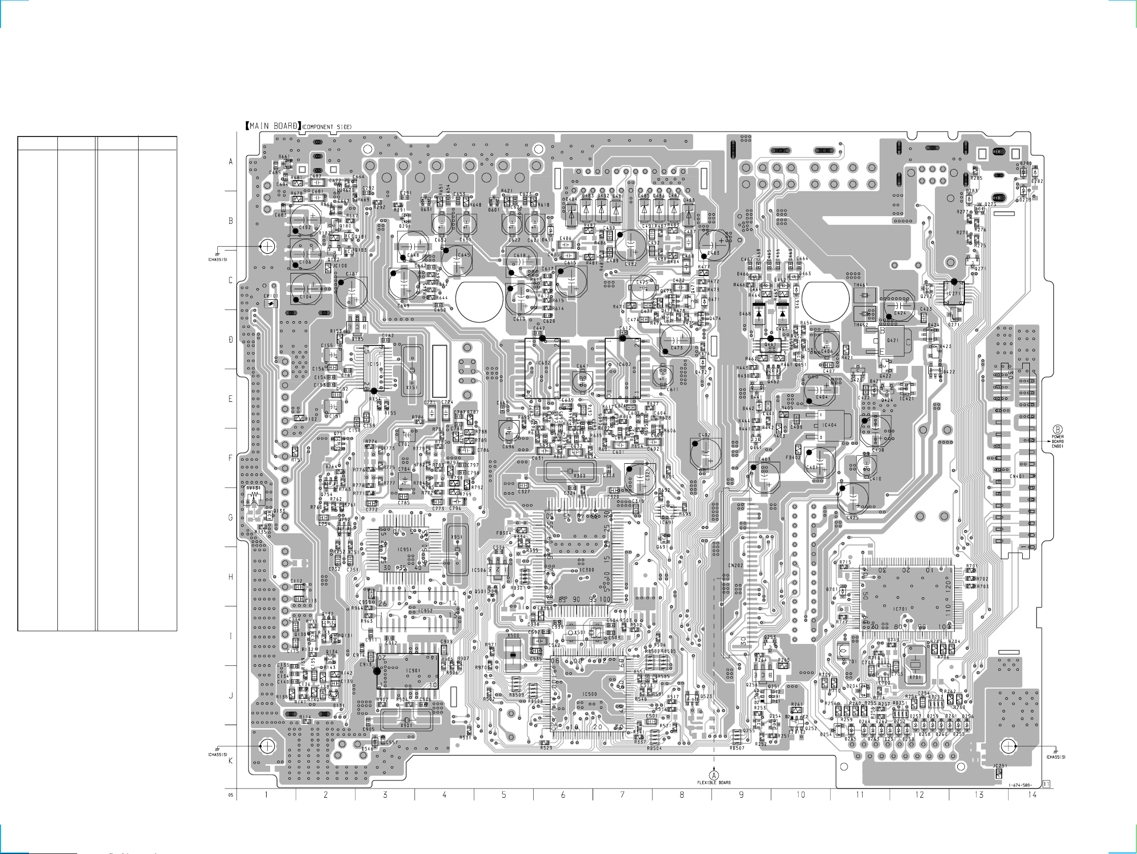
5-10. Printed Wiring Board
– MAIN Board (Component Side) – .............................. 30
5-11. Printed Wiring Board
– MAIN Board (Conductor Side) – ................................ 31
5-12. Schematic Diagram – MAIN Board (1/5) – .................. 32
5-13. Schematic Diagram – MAIN Board (2/5) – .................. 33
5-14. Schematic Diagram – MAIN Board (3/5) – .................. 34
5-15. Schematic Diagram – MAIN Board (4/5) – .................. 35
5-16. Schematic Diagram – MAIN Board (5/5) – .................. 36
5-17. Printed Wiring Boar d – POWER Board – ..................... 38
5-18. Schematic Diagram – POWER Board –........................ 39
5-19. Printed Wir ing Board – DISPLAY Board – .................. 40
5-20. Schematic Diagram – DISPLAY Board – ..................... 41
5-21. Printed Wiring Board – RELAY Board – ...................... 42
5-22. Schematic Diagram – RELAY Board – ......................... 43
5-23. IC Pin Function Description ........................................... 52
6. EXPLODED VIEWS ................................................ 66
7. ELECTRICAL PARTS LIST ............................... 70
2
Page 3
SECTION 1
IC803
MSM534001E-49TSKFDR3 (TYPE C: ENGLISH, FRENCH)
MSM534001E-50TSKFDR3 (TYPE A: ENGLISH, SPANISH)
MSM534001E-51TSKFDR3 (TYPE B: ENGLISH, GERMAN)
SERVICE NOTE
NOTES ON HANDLING THE OPTICAL PICK-UP
BLOCK OR BASE UNIT
The laser diode in the optical pick-up block may suffer electrostatic break-down because of the potential difference generated
by the charged electrostatic load, etc. on clothing and the human
body.
During repair, pay attention to electrostatic break-down and also
use the procedure in the printed matter which is included in the
repair parts.
The flexible board is easily damaged and should be handled with
care.
NOTES ON LASER DIODE EMISSION CHECK
Never look into the laser diode emission from right avove when
checking it for adustment. It is feared that you will lose your sight.
NOTES ON HANDLING THE OPTICAL PICK-UP BLOCK
(KMS-241B/J1NP)
The laser diode in the optical pick-up block may suffer electrostatic break-down easily. When handling it, perform soldering
bridge to the laser-tap on the flexible board. Also perform m easures
against electrostatic break-down suff iciently before the operation.
The flexible board is easily damaged and should be handled with
care.
• Model Identification
The destination is expressed with the model according to the language of Program Rom mounted in the set.
How to identify the model is described below.
– POWER BOARD (Component Side) –
laser-tap
OPTICAL PICK-UP FLEXIBLE BOARD
Notes on chip component replacement
• Never reuse a disconnected chip component.
• Notice that the minus side of a tantalum capacitor may be damaged by heat.
Flexible Circuit Board Repairing
• Keep the temperature of the soldering iron around 270 ˚C during repairing.
• Do not touch the soldering iron on the same conductor of the
circuit board (within 3 times).
• Be careful not to apply force on the conductor when soldering
or unsoldering.
CAUTION
Use of controls or adjustments or performance of procedures
other than those specified herein may result in hazardous radiation exposure.
SAFETY-RELATED COMPONENT WARNING!!
COMPONENTS IDENTIFIED BY MARK ! OR DOTTED
LINE WITH MARK ! ON THE SCHEMATIC DIAGRAMS
AND IN THE PARTS LIST ARE CRITICAL TO SAFE
OPERATION. REPLACE THESE COMPONENTS WITH
SONY PARTS WHOSE PART NUMBERS APPEAR AS
SHOWN IN THIS MANUAL OR IN SUPPLEMENTS PUBLISHED BY SONY.
3
Page 4
SECTION 2
GENERAL
This section is extracted from
instruction manual.
4
Page 5
56789
Page 6
Page 7
Page 8
Page 9
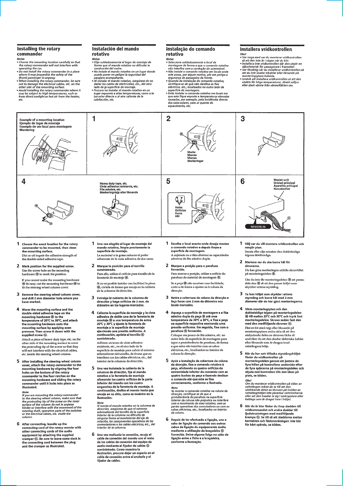
Installation for Microphone and Rotary Commander
Page 10
10
Page 11
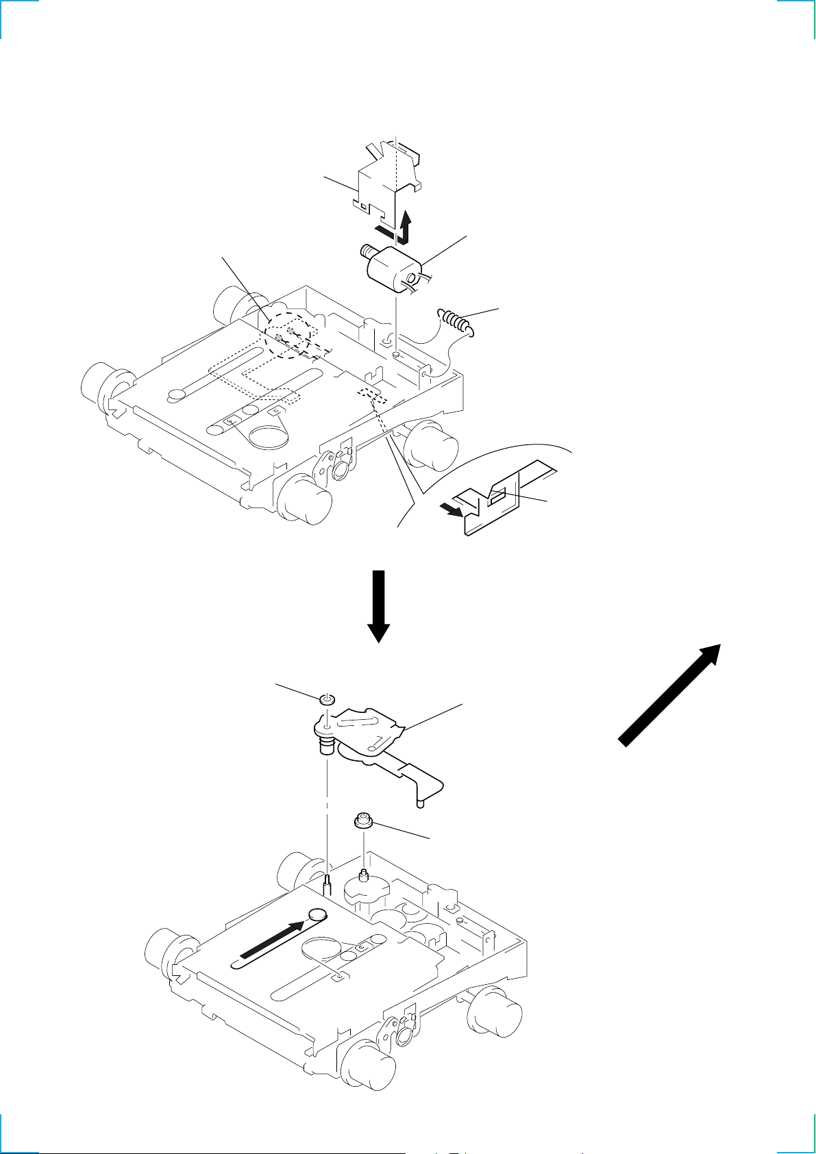
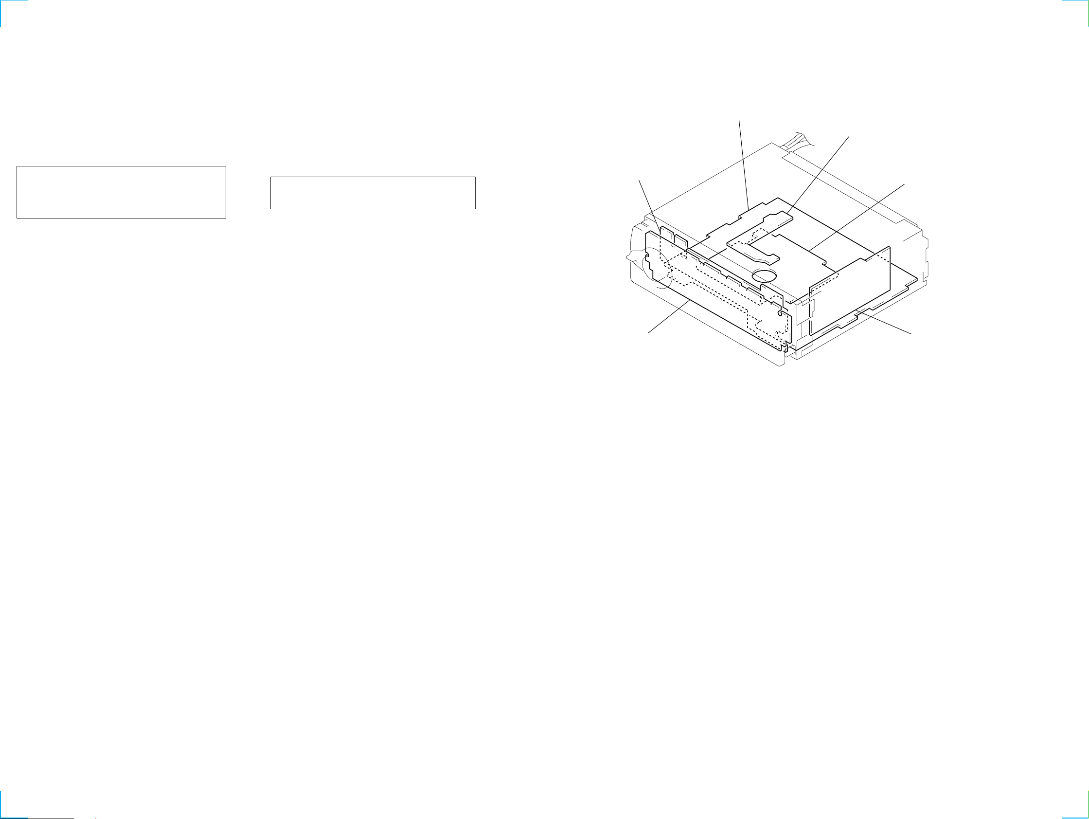
SECTION 3
DISASSEMBLY
Note: Follow the disassembly procedure in the numerical order given.
SUB PANEL ASS’Y
2
two claws
4
sub panel ass’y
1
three screws
(PTT2.6
×
6)
2
claw
MECHANISM DECK (MG-164NF-138)
3
connector
(CN701)
1
screw
(PTT2.6
1
two screws
(PTT2.6
×
6)
×
4)
2
mechanism deck
(MG-164NF-138)
3
flexible board
(CN202)
11
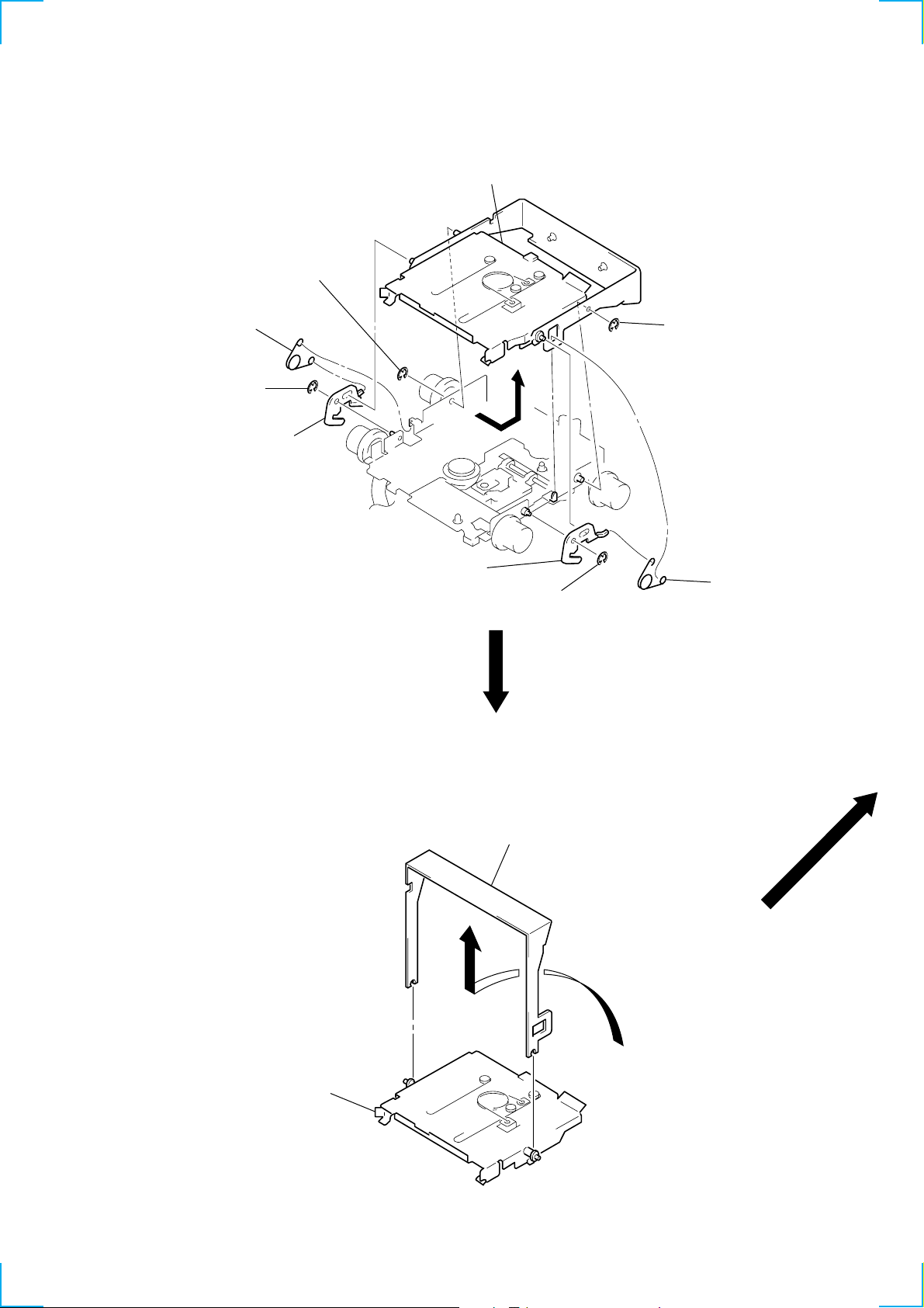
Page 12
SERVO BOARD
2
sensor flexible board
(CN102)
3
two screws
(BVTT2
1
flexible board
3
two screws
(BVTT2
4
1
(CN101)
×
4 )
servo board
flexible board
(CN103)
×
4)
MAIN BOARD
6
Remove the solder of the cord
(with connector) (ANT).
3
three ground point screws
5
4
main board
insulating sheet
1
two connectors
(CN101, 291)
9
cord (with connector)
(RCA)
7
two screws
(PTT2.6
8
cord (with connector)
(ANT)
×
10)
0
seven screws
(PTT2.6
!¡
Remove the heat sink
in the direction of the arrow.
×
10)
2
two screws
(PTT2.6
×
10)
12
Page 13
MD COVER ASS’Y
s
1
spring (float B)
1
spring (float B)
2
two springs (float F)
3
Pushing the arrow A part,
raise the float block upward at the front to unlock.
A
float block
lever (lock R)
lever (lock L)
3
MD cover ass’y
cassette holder
shaft (MD cover guide)
1
four screw
(B2 × 3)
FLOAT BLOCK
A
2
Pushing the cassette holder in the arrow A direction with a screwdriver,
disengage the shaft (MD cover guide) from the groove of MD cover ass’y.
Note : Be careful not to damage the optical pick-up
when pushing the cassette holder with a screwdriver.
13
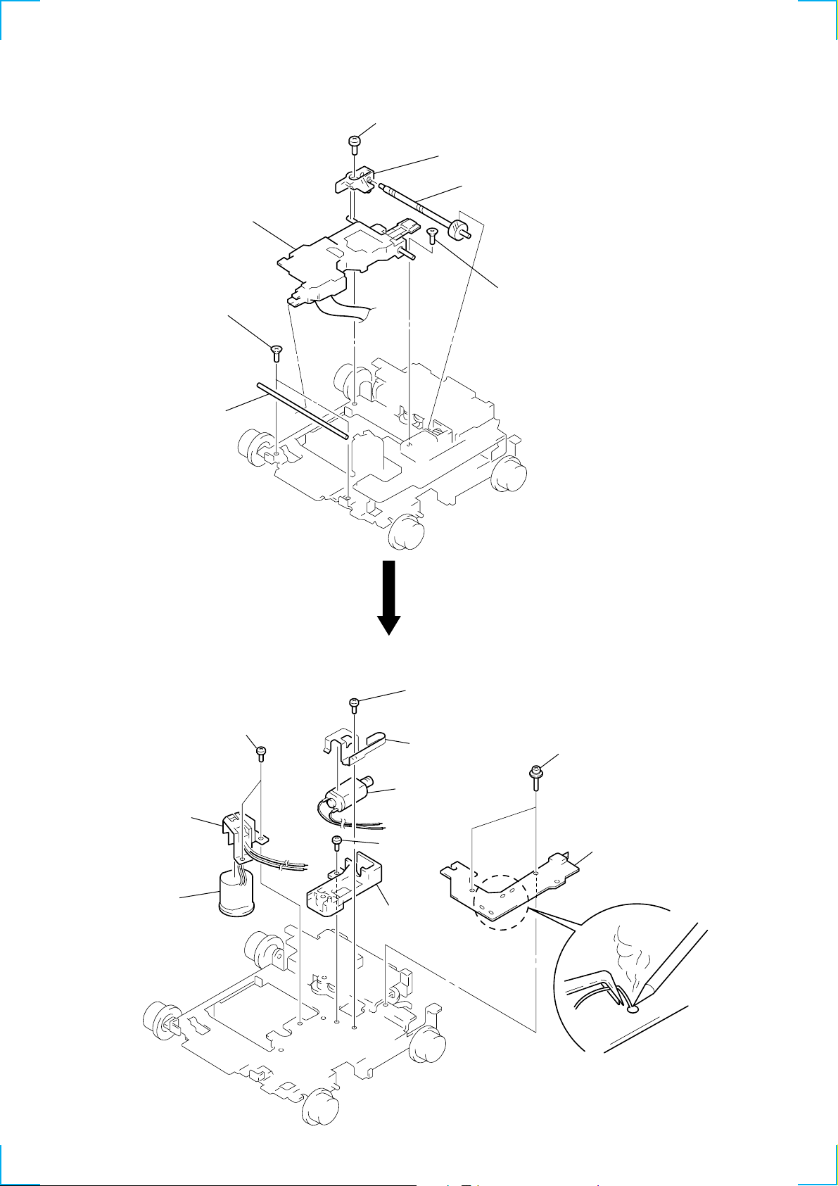
Page 14
LO MOTOR ASS’Y (LOADING) (M903)
)
4
Remove the bracket (LO)
in the direction of the arrow
A
.
1
Remove solder of the motor (M903).
A
5
LO motor ass’y (loading) (M903
2
spring (rack)
3
claw
LEVER ASS’Y (LE)
2
stopper washer
1
3
4
roller (gear E)
lever ass’y (LE)
14
Page 15
HOLDER ASS’Y
1
spring (CHKG)
2
stop ring E (1.5)
3
lever (lock R)
4
stop ring E (1.5)
5
Remove the holder ass’y
in the direction of the arrow.
3
lever (lock L)
2
stop ring E (1.5)
4
stop ring E (1.5)
1
spring (CHKG)
CHUCKING ARM ASS’Y
holder ass’y
1
Remove the chucking arm ass’y
in the direction of the arrow.
15
Page 16
OPTICAL PICK-UP (KMS-241B/J1NP)
y
7
optical pick-up
(KMS-241B/J1NP)
1
two screws
(K2
×
3)
2
shaft (OPTL)
4
screw
(B2
×
3)
6
bearing (SL)
5
feed screw ass’
3
screw
(K2
×
3)
SL MOTOR ASS’Y (SLED) (M902)/SP MOTOR ASS’Y (SPINDLE) (M901)
4
screw
(P1.7
×
1.8)
bracket (SL)
3)
0
!¡
SP motor ass’y
(spindle) (M901)
9
bracket (SP)
two screws
×
1.8)
(P1.7
7
screw
(B2
8
5
6
base (SL)
SL motor ass’y
(sled) (M902)
×
2
two screws
(PSW2
×
8)
3
sensor board
16
1
Remove solders
of motors (M901, 902).
Page 17
SECTION 4
)
SHUF
SHUF
ELECTRICAL ADJUSTMENTS
TEST MODE
This set have the test mode function. In the test mode, FM Auto
Scan/Stop Level and MW Auto Scan/Stop Level adjustments can
be performed easier than it in ordinary procedure.
<Set the Test Mode>
1. Turn ON the regulated power supply. (All LEDs on the set
lights up, and the clock is displayed.)
Note: Press the [OFF] button, if the clock is not displayed.
2. Push the preset [4] button.
3. Push the preset [5] button.
4. Press the preset [1] button for more than two seconds.
5. Then the display indicates all lights, the test mode is set.
<Release the Test mode>
1. Push the [OFF] button.
See the adjustment location from on page 20 for the adjustment.
MD SECTION
MD section adjustments are done automatically in this set.
TUNER SECTION
0 dB=1 µV
Cautions during repair
When the tuner unit is defective, replace it by a new one because its internal block is difficult to repair.
Note: Adjust the tuner section in the sequence shown below.
1. FM Auto Scan/Stop Level Adjustment
2. FM Stereo Separation Adjustment (Wide)
3. FM Stereo Separation Adjustment (Narrow)
4. FM RDS S-Meter Adjustment
5. MW Auto Scan/Stop Level Adjustment
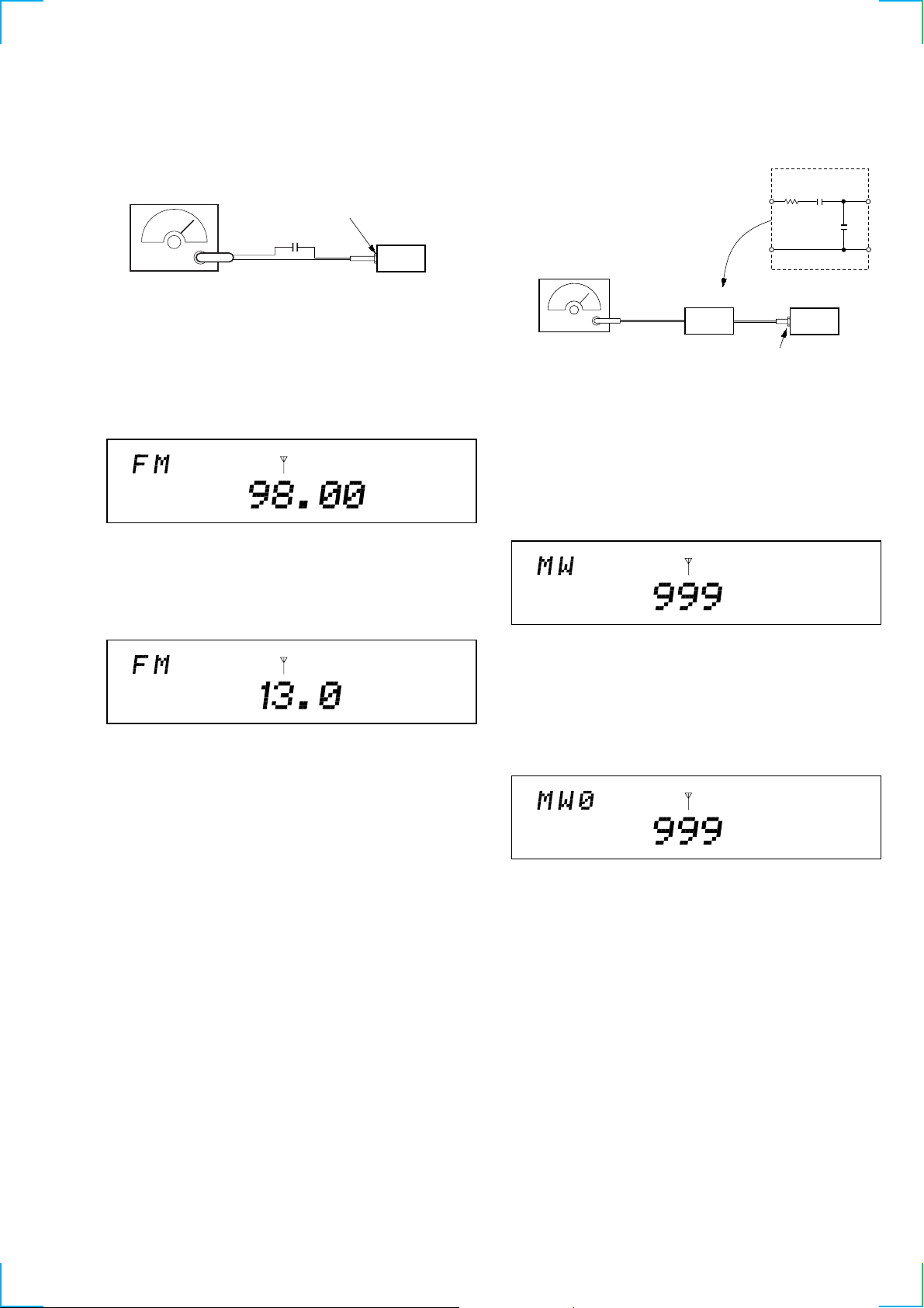
FM Auto Scan/Stop Level Adjustment
Setting:
[SOURCE] button : FM
FM RF signal
generator
Carrier frequency : 98.00 MHz
Output level : 22 dB (12.6
Mode : mono
Modulation : 1 kHz, 22.5 kHz deviation (30%
Procedure:
1. Set to the test mode.
2. Push the
[SOURCE] button and set to FM.
0.01 µF
antenna jack
µ
V)
set
Display
3. Adjust the v olume RV2 on TU101 by turning clockwise untill
“0” is shown next to “FM” on the display window, If “0” is
already shown or the volume RV2 has been turned too far,
turn it back counterclockwise untill “0” is disappeared once,
then try this adjustment.
Display
Adjustment Location: See page 20.
17
Page 18
FM Stereo Separation Adjustment (Wide)
Setting:
[SOURCE] button : FM
FM Stereo Separation Adjustment (Narrow)
Setting:
[SOURCE] button : FM
FM RF signal
generator
Carrier frequency : 98.00 MHz
Output level : 70 dB (3.2 mV)
Mode : stereo
Modulation : main: 1 kHz, 20 kHz deviation (26.5%)
antenna jack
0.01 µF
(75
Ω)
sub : 1 kHz, 20 kHz deviation (26.5%)
: 19 kHz pilot: 7.5 kHz deviation (10%)
set
10 k
LINE OUT jack (CNP601)
Ω
level meter
+
–
Procedure:
1. Set to the test mode. (See page 17)
2. Push the
[SHIFT] button.
3. Push the [4] button four times.
4. Push the [5] button once and set to wide mode.
5. Adjust the v olume R V3 on FM/AM tuner unit (TU101) f or the
best separation.
FM Stereo
signal generator
output channel
L-CH L-CH A
L-CH R-CH Adjust RV3 on TU101
R-CH R-CH C
R-CH L-CH D
Level meter Level meter
connection reading (dB)
B
for minimum reading.
L-CH Stereo separation: A-B
R-CH Stereo separation: C-D
The separations of both channels should be equal.
FM RF signal
generator
Carrier frequency : 98.00MHz
Output level : 70 dB (3.2 mV)
Mode : stereo
Modulation : main: 1 kHz, 20 kHz deviation (26.5%)
antenna jack
0.01 µF
Ω)
(75
sub : 1 kHz, 20 kHz deviation (26.5%)
: 19 kHz pilot: 7.5 kHz deviation (10%)
set
10 k
LINE OUT jack (CNP601)
Ω
level meter
+
–
Procedure:
1. Set to the test mode. (See page 17)
2. Push the
[SHIFT] button.
3. Push the [4] button four times.
4. Push the [5] button twice and set to narrow mode.
5. Adjust the v olume RV4 on FM/AM tuner unit (TU101) for the
best separation.
FM Stereo
signal generator
output channel
L-CH L-CH A
L-CH R-CH Adjust RV4 on TU101
R-CH R-CH C
R-CH L-CH D
Level meter Level meter
connection reading (dB)
B
for minimum reading.
L-CH Stereo separation: A-B
R-CH Stereo separation: C-D
The separations of both channels should be equal.
Specification: Separation more than 24 dB
Adjustment Location: See page 20.
Specification: Separation more than 18 dB
Adjustment Location: See page 20.
18
Page 19
FM RDS S-Meter Adjustment
µ
SHUFTPSHUF
TP
Setting:
[SOURCE] button : FM
MW Auto Scan/Stop Level Adjustment
Setting:
[SOURCE] n [MODE] button : MW
FM RF signal
generator
Carrier frequency : 98.00 MHz
Output level : 35 dB (56.2
Mode : mono
Modulation : no modulation
0.01
antenna jack
µ
F
µ
V)
set
Procedure:
1. Set to the test mode. (See page 17)
2. Push the
[SOURCE] button and set to FM.
Display
SHUF
3. Push the preset
[10] button .
4. Adjust RV131 on MAIN board so that the display indication
is “13.0”.
Display
AM RF signal
generator
AM dummy antenna
(50 Ω)
Carrier frequency : 999 kHz
30% amplitude
modulation by
1 kHz signal
Output level : 33 dB (44.7
Procedure:
1. Set to the test mode. (See page 17)
2. Push the
3. Push the
[SOURCE] button and set to FM.
[MODE] button and set to MW.
Display
V)
30
Ω
15 pF
65 pF
set
antenna jack
SHUF
Specification: Display indication: 12.8 to 13.2.
Adjustment Location: See page 20.
4. Adjust the v olume RV1 on TU101 by turning clockwise untill
“0” is shown next to “MW” on the display window, If “0” is
already shown or the volume RV1 has been turned too far,
turn it back counterclockwise untill “0” is disappeared once,
then try this adjustment.
Display
Adjustment Location: See page 20.
19
Page 20
Adjustment Location:
– SET UPPER VIEW –
TU101
RV131
FM RDS S-Meter
Adjustment
RV1
MW Auto Scan/Stop
Level Adjustment
RV2
FM Auto Scan/Stop
Level Adjustment
RV3
FM Stereo Separation
Adjustment (Wide)
RV4
FM Stereo Separation
Adjustment (Narrow)
Front
20
Page 21
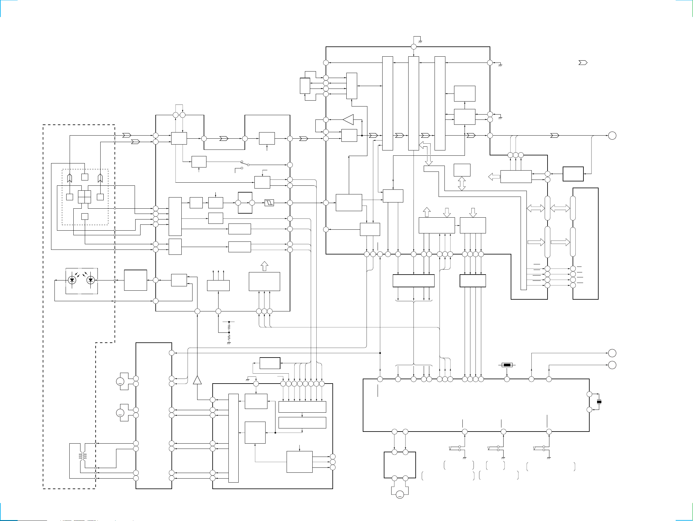
SECTION 5
DIAGRAMS
MDX-C8970R
5-1. BLOCK DIAGRAM – SERVO Section –
I
J
F
C B
I J
D A
E
DETECTOR
LASER DIODE
OPTICAL PICK-UP
(KMS-241B/J1NP)
2-AXIS
DEVICE
(FOCUS)
(TRACKING)
05
LDPD
ILCC
PD
M901
(SPINDLE)
M902
(SLED)
FCS+
FCS–
TRK+
TRK–
B
A
C
D
E
F
AUTOMATIC
POWER
CONTROL
Q302
FOCUS/TRACKING COIL DRIVE,
SPINDLE/SLED MOTOR DRIVE
6
27
25
21
23
12
10
8
OUT4F
OUT4R
OUT2F
OUT2R
OUT1F
OUT1R
OUT3F
OUT3R
M
M
IC303
I
1
J
2
A
4
B
5
C
6
D
7
E
8
F
9
APC
11
PD
10
IN4R
IN4F
IN2F
IN2R
IN1F
IN1R
IN3F
IN3R
RF AMP
I-V
AMP
I-V
AMP
16PSB
3
4
29
30
19
18
14
15
48 47
MORFO
LD/PD
AMP
SPFD
SPRD
MORFI
RFO
B.P.F.
3T
AT
AMP
APCREF
12
LEVEL SHIFT
46
IC306
WBL
B.P.F.
ABCD
AMP
WBL3TEQ
V-I
CONVERTER
F0CNT
20
APCREF
83
SFDR
92
SRDR
91
FFDR
88
FRDR
89
TFDR
86
TRDR
85
FOCUS/TRACKING ERROR AMP
AGCI
40
TEMP
ADFM
29 30
FOCUS
ERROR AMP
TRACKING
ERROR AMP
+3.3V
AUTOMATIC
CONTROL
DIGITAL
SERVO
SIGNAL
PROCESS
PWM GENERATOR
RF AMP,
IC302
RF AGC
& EQ
EQ
WBL
PEAK &
BOTTOM
ADIN
COMMAND
SERIAL/
PARALLEL
CONVERTER,
DECODER
XLAT
SCLK
SWDT
1716 18
PEAK HOLD
Q301
+3.3V
13
RECP
POWER
DIGITAL SERVO
SIGNAL PROCESSOR
IC301 (2/2)
RF
AUX
PEAK
BOTM
ADFG
ABCD
FE
TE
SE
ABCD
AUX1
38
33
37
36
32
35
34
26
28
7465647566 63
FE
TE
AUX2
ABCD
ANALOG MUX
A/D CONVERTER
FROM CPU
INTERFACE
AUTO
SEQUENCER
FILTER
73 62
SE
PEAK
XLRF
CKRF
DTRF
100
59
58
61
60
51
52
55
78
79
BOTM
EFMO
FILI
PCO
CLTV
FILO
ASYO
ASYI
COMPA-
RFI
RATOR
ADIP
ADFG
DEMODULATOR/
DECODER
F0CNT
80
81
82
PLL
15
TX
EFM/ACIRC
ENCODER/DECODER
SUBCODE
PROCESSOR
SPINDLE
SERVO
SPFD
SPRD
DQSY11SQSY14XINT
XRST
94 93
10
12
59 62 55 54 52 45 51 64 26 27 28 29
MD-RST
7 6
LOADING
MOTOR DRIVE
IC305
M903
(LOADING)
5
RIN FIN
OUT1 OUT2
1 7
SHOCK PROOF
MEMORY CONTROLLER
51331
LEVEL SHIFT
IC502
61242
SQSY
CC-XINT
EJECT
LOAD
4
M
ATRAC
CPU
INTERFACE
SENS
SRDT
SWDT
9 8 5 6 7
SWDT
SENS
MD-SI
MD-SO
ON: When the disc loading start
and the disc eject completion.
IC301 (1/2)
SAMPLING
RATE
CONVERTER
DIGITAL
AUDIO
ENCODER/DECODER
INTERFACE
D-RAM
INTERNAL BUS
MONITOR
CONTROL
SCLK
XLAT
MNT0
MNT1
MNT2
1 2 3 4
135
13
LEVEL SHIFT
IC503
246
12
FOK
SHOCK
XBUSY
SCLK
XLAT
MNT0
MD-LAT
MD-CKO
LOADING START/
EJECT END
MNT1
MD MECHANISM CONTROLLER
IC501 (1/2)
C-SW
63
ADDT
23
DIGITAL SIGNAL PROCESSOR,
EFM/ACIRC ENCODER/DECODER,
SHOCK PROOF MEMORY CONTROLLER,
ATRAC ENCODER/DECODER, 2M BIT D-RAM
DIN
21
DOUT
22
DADT
24
MNT3
SLOCK
MNT2
MNT3
LOADING
END
ON: When completion of
the disc loading.
IC301 (1/2)
BCK
LRCK
2526 27
XBCK
LRCK
FS256
CLOCK
GENERATOR
TH501
39
TEMP
E-SW
11 56
DADT, BCK, LRCK, 512FS
LOCK
LIMIT-IN
512FS
BUFFER
IC304
OSCI
16
OSCO
17
D0 – D3A00 – A09
47, 46, 48, 49
32 – 29, 34 – 38, 43
XOE
41 22
XWE
45 3
XRAS
44 4
XCAS
42 23
EMPHASIS
66
21
DEEMP
(LIMIT)
ON: When the optical pick-up is
inner position.
• SIGNAL PATH
: MD PLAY
512FS
D0 – D3
1, 2, 24, 25
A0 – A9
9 – 12, 14 – 18, 5
OE
WE
RAS
CAS
D-RAM
IC307
EMPHASIS
LOCK
31
EXTAL
XTAL
32
(Page 23)
(Page 23)
(Page 24)
X501
10MHz
A
B
C
2121
Page 22
MDX-C8970R
5-2. BLOCK DIAGRAM – TUNER Section –
CN101
ANT
FM/AM TUNER UNIT
TU101
FM-ANT
2
1
AM-ANT
VCO11AM-IF
LO/DX
4
6
5 24 14
25
FM IN
AM IN
LO/DX
OSCI
OSCO
X151
10.25MHz
FM-IF
21
15
IF FM
IF AM
FM/AM PLL
IC151
5
28
LP OUT
VT
169 10 13 12
FILTER
1
LP FM
SSTOP
2
LP HC
SDA
3
SCL
LP AM
FM B+
AM B+
TUNER B+
8
10
9
18
FM +B
AM +B
+B (FM/AM)
SEEK
ST/MONO
13
20SD22
FORCED
24
WIDE/NARROW
SWITCH
Q132
RV131
FM RDS
S-METER
WIDE/NARROW
SWITCH
Q131
S-METER
19
FM/AM SIGNAL
METER BUFFER
Q133
S-METER
(RDS)
15
FM LCH
16
FM RCH
AM DET
FM DET
MPX
57 kHz
BAND-PASS
FILTER
16
R-CH
12
23
BUFFER
Q130
LIN
BAND-PASS
FILTER
IC131
NOISE DET
DISCHARGE
Q134
RDS DECODER
OUT
IC901
SC
CIN
19
CLOCKED
COMPARATOR
18
SIGNAL
QUALITY
DECODER
RDS/RDBS
DEMODULATOR
& DECODER
5
4
INTERFACE
REGISTER
MUTING
Q752
R-CH
MUTING
Q753
AM
ON
202619
D751
AM/TIR SIGNAL SELECT
SWITCH
IC752
6 5
3
1 2
7
SADX
REGISTER
CONTROLLER
RWCK
OSC
XT
48
X951
4.19MHz
Q754 (2/2)
CS1
CS2
TAS
SAS
WE
DI/O
XT
47
Q754 (1/2)
TRAFFIC INFORMATION REPLAY
18
L.P.F.
FOUT
AOUT
17
11
FIN
ADIN
16
CPU INTERFACE
CE1
RDWRCE2
56
TIR RD
TIR WR
TIR CE0
TIR CE1
IC951
D/A
CONVERTER
A/D
CONVERTER
D0 – D3
1 – 4
TIR D3
TIR D0 –
ADPCM
STATUS
REGISTER
BUSY
ANALYZER/
SYNTHESIZER
ADDRESS
CONTROLLER
DATA I/O
TIMING
CONTROLLER
RESET
PDWN
5355455
35
40
41
39
37
36
46
50
44
FM
(Page 23)
CONTROL SWITCH
AM/TIR
(Page 23)
D
MUTING
Q751
E
SERIAL REGISTER
IC952
14
CS
SAD
17
TAS
15
16
SAS
13
WE
2
RWCK
DIN
8
DOUT
12
• SIGNAL PATH
: FM
: MW/LW
20
120
70 71
SSTOP
I2C-DATA
05
I2C-SCL
117
23
SEEK
29
SD-IN
ST/MONO
32
NARROW
31
WIDE
46
VSM
(S-METER)
PATH
DETECTOR
MASTER CONTROLLER
IC500 (1/4)
MULTI
LVIN
MPTH
2
53
X901
4.332MHz
MTP
OSCILLATOR
& CLOCK
OSCI
OSCO
4
5
DAVN
8
67
RDS-DAVN
IIC BUS
SLAVE
TRANSCEIVER
SDA
SCL
9
10
116
52
NS-MASK
QUALITY
106
TIR-CE0
105
TIR-CE1
103
104
TIR-RD
TIR-WR
99 – 102
–
TIR-D0
TIR-D3
3
TIR-BUSY
5
TIR-RST
4
TIR-PDOWN
118
10
TIR-PLAY
AF-MUTE
2222
Page 23
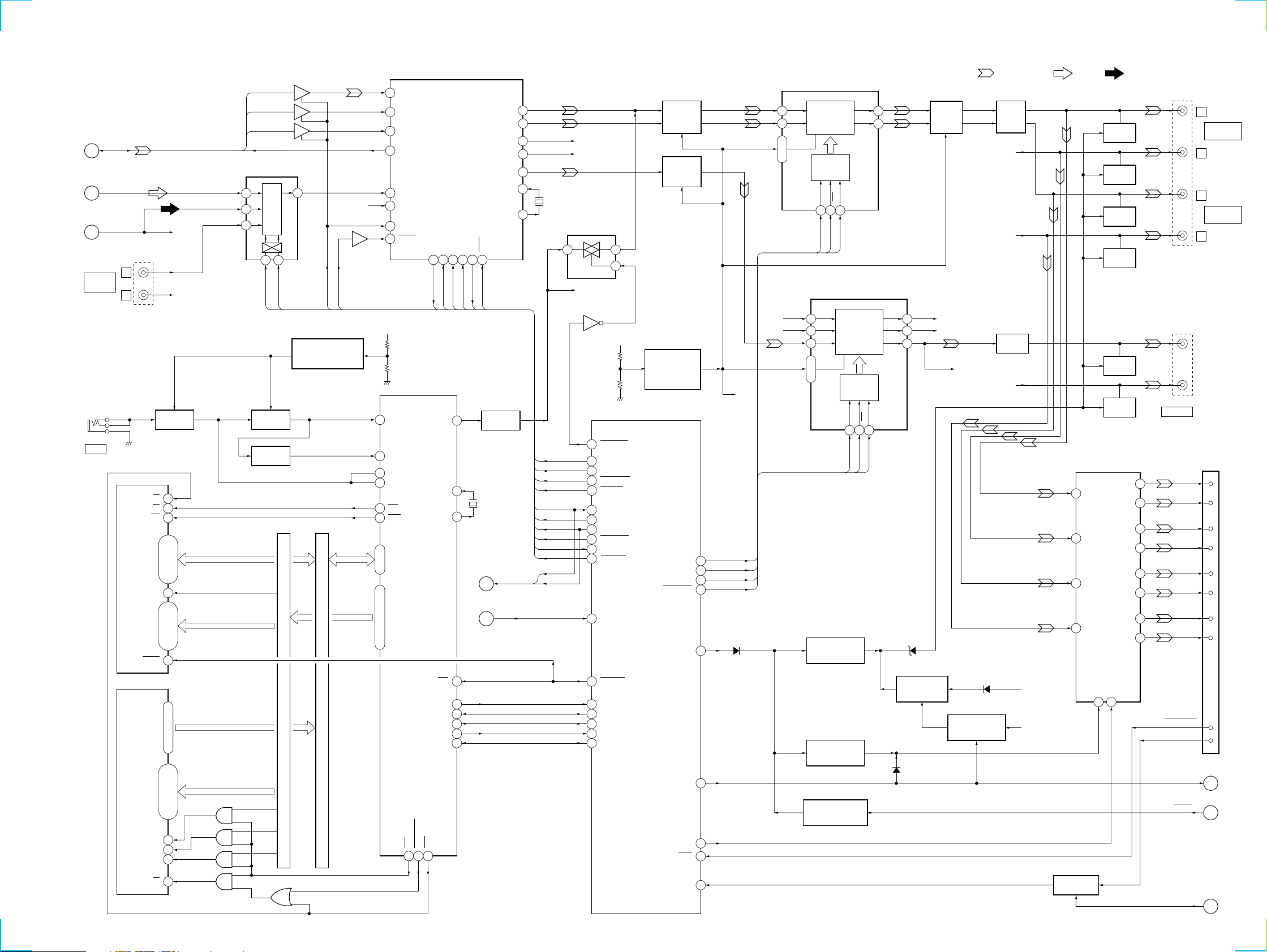
MDX-C8970R
5-3. BLOCK DIAGRAM – MAIN Section –
LEVEL SHIFT
IC351 (1/2)
DADT
9
LRCK
2
A
(Page 21)
D
(Page 22)
E
(Page 22)
CNP601 (1/2)
BUS
AUDIO IN
CNJ252
MIC
DADT,
BCK,
LRCK,
512FS
FM
AM/TIR
L
R
FLASH
MEMORY
IC805
WE
A-1
RESET
MIC AMP
IC841 (1/3)
28
OE
26
CE
11
D0 – D7
29, 31, 33, 35,
45
A0 – A18
25 – 18, 8 – 1,
12
FM-IN-L
AM-IN-L
AUX-IN-L
R-CH
R-CH
D0 – D7 D0 – D7
38, 40, 42, 44
A0
A1 – A19
48, 17, 16
BCK
512FS
INPUT SELECT
IC771
20
18
16
8 9
SEL0
BUFFER
IC841 (2/3)
BUFFER
IC841 (3/3)
5
14
INPUT
SELECTOR
SEL1
REFERENCE VOLTAGE
GENERATOR (FOR BIAS)
ADDRESS BUS
8
10
3
1
6
4
XMST
IC843 (2/2)
DATA BUS
R-CH
12
LEVEL SHIFT
IC351 (2/2)
DSPSTP
A0 – A19
SI1
71
76
LRCK
75
BCK
81
PLCLK
35
LIN
46
RIN
77
XMST
11
82
CKSTP
+5V
51
AN0
50
AN1
P07
32
33
P06
27
FCE
45
WRD
64 – 57
D0 – D7
A0 – A19
18 – 11, 8 – 1, 31-28
DIGITAL SIGNAL PROCESSOR,
DIGITAL FILTER,
D/A CONVERTER
IC300
XLAT
RVDT59SCK
RVDT
62 57
XLAT
SCK
48
20
19
REDY
6061
REDY
(Page 24)
(Page 21)
CSV
IC801
TRDT
63
TRDT
DAC
XI1
XO1
AOUTL1
AOUTR1
AOUTR3
AOUTL3
AOUTR2
XTLI38
XTLO38
XRST
DSPRST
BUFFER
IC843 (1/2)
X801
14.318MHz
DSPCK,
SA DATA
F
EMPHASIS
B
27
29
54
52
43
41
40
FL-OUT
RL-OUT
FR-OUT
RR-OUT
SUB-OUT
16.9344MHz
SEL0
SEL1
XMST
DSPSTP
TRDT
RVDT
SCK
XLAT
REDY
DSPRST
SA DATA
DSPCK
R-CH
R-CH
X300
CSV MIX SWITCH
IC691
1 2
R-CH
Q691
7
AUDIO +8.5V
CSV-PLAY
11
AUDIO SEL0
37
40
AUDIO SEL1
DSP-XMST
30
9
DSPSTP
17
DSP-SI
DSP-SO
18
19
DSPCK
DSP-XLAT
59
79
DSP-REDY
28
DSP-RST
81
EMPH
MASTER CONTROLLER
CENTER VOLTAGE
GENERATOR
IC500 (2/4)
LOW-PASS
FILTER
IC601
LOW-PASS
FILTER
IC661 (1/2)
(FOR BIAS)
IC661 (2/2)
VOL-DATA-L
VOL-DATA-R
VOL-CLK
VOL-LOAD
MUTE
ELECTRICAL
VOLUME
IC602
IN1
IN2
GND 1-3
5, 1, 17
RESISTIVE
NETWORK &
TAP SWITCHES
SHIFT
REGISTER &
LATCH
D-IN
11 9 10
DAT-L
IN1
4
IN2
2
IN3
18
GND 1-3
5, 1, 17
CONTROL SWITCH
4
2
R-CH
R-CH
R-CH
DAT-L
56
DAT-R
57
58
55
36
CLK
LOD
D527
L/S
CLK
CLK
LOD
ELECTRICAL
NETWORK &
TAP SWITCHES
REGISTER &
MUTING
Q473
OUT1
OUT2
VOLUME
IC632
RESISTIVE
SHIFT
LATCH
D-IN
CLK
11 9 10
CLK
DAT-R
L/S
LOD
6
20
OUT1
OUT2
OUT3
6
20
16
D491
BUFFER
IC603
R-CH
R-CH
R-CH
: MD PLAY : FM : MW/LW
LINE
DRIVER
IC604
R-CH
R-CH
BUFFER
IC663
R-CH
12
14
11
15
POWER AMP
IC481
IN2
IN4
IN1
IN3
MUTING
Q601
MUTING
Q602
MUTING
Q631
MUTING
Q632
MUTING
Q661
MUTING
Q662
OUT2+
OUT2–
OUT4+
OUT4–
OUT1+
OUT1–
OUT3+
OUT3–
5
3
21
23
9
7
17
19
CNP601 (2/2)
L
R
L
R
(L)
(R)
CN291
SUB OUT
CNP401 (1/2)
(POWER CONNECTOR)
FRONT
LINE OUT
REAR
LINE OUT
1
9
4
12
2
10
3
11
FL+
FL–
FR+
FR–
RL+
RL–
RR+
RR–
• SIGNAL PATH
21
RST
38
DO
DI
D0 – D7
D0 – D7
21 – 23, 25 – 29
PROGRAM
ROM
IC803
A0 – A15
20 – 13, 3, 2, 31
A16
10
A17
6
A18
7
32
OE
05
1, 12, 4, 5, 11
A0 – A15
6
11
8
3
SWITCHING
IC802
1
2
DATA BUS
SWITCHING
IC804
RDC44RDD
42
26
ADDRESS BUS
A16
4
5
A17
12
13
A18
9
10
2
1
4
CLK
REQ
ROMCONT
36
39
35
37
CE
112
25
26
27
110
111
CSV-RST
CSV-SI
CSV-SO
CSV-CK
CSV-REQ
CSV-CE
POWON
AMP-STBY
TEST
TEL-MUTE
BATTERY OFF
MUTE DRIVER
Q472
MUTING
CONTROL SWITCH
Q471
62
RESET SWITCH ON
MUTING DRIVER
Q501
98
80
83
D471
D472
MUTING
CONTROL SWITCH
Q474
AUDIO +8.5V
BATT B+
LEVEL SHIFT
Q451
22
MUTE
4
STBY
TEST MODE
TEL-ATT
POW-ON
RESET
TEL 5V
15
13
G
(Page 25)
H
(Page 25)
I
(Page 24)
2323
Page 24
MDX-C8970R
5-4. BLOCK DIAGRAM – DISPLAY/KEY CONTROL Section –
(Page 23)
(Page 21)
REMOTE IN
DSPCK, SA DATA
F
LOCK
C
CNJ272
48
D282
49 60
RC-IN0
DSPCK
63
RC-IN1
78
SA DATA
33
61
LSW702, 900 – 918,
SP-LAT
S900
47
KEY-IN0
48
KEY-IN1
X701
18.432MHz
86
DOOR-IND
X0A
74
TEL 5V
I
BATT B+
LCD +10V
(Page 23)
ROTARY
ENCODER
RE900
D254
1 2
RE-IN1
RE-IN0
LED705
TIR
LED DRIVE
Q252
85
45
RE900
VOLUME/BASS/
TREBLE/BALANCE/
FADER CONTROL
DOOR-SW
115
CN702
MAIN BODY SIDE
54
76
KEYACK
CN800
FRONT PANEL SIDE
9 10
KEY ACTIVE
SWITCH
Q523
107
AD-ON
MASTER CONTROLLER
IC500 (3/4)
41
BACKUP +5V
LCDANG
(NOSE DETECT)
109
NOSE-SW
S500
BUZZER
DRIVE
Q504
15
BEEP
BZ500
(BUZZER)
LED706
(MD DISC SLOT),
LSW702
P-ON +10V
§
P-ON +10V
SWITCH
Q904
X1
93
X500
3.58MHz
LED DRIVE
Q251
95
X0
92
X1A
73
X501
32.768kHz
SP-SI
SP-LAT
SP-SCK
MD-LOCK
LCD CE1
70
R924
OSC
13
OSCOUT
05
12
OSCIN
LIQUID CRYSTAL
DISPLAY DRIVER
SEG66 – SEG121
25 – 80
9
IC920
CE1
8
7
DATA
CLK
10
OE
VLC0 – VLC3
COM0 – COM3
LIQUID CRYSTAL DISPLAY
16 – 19
21 – 24
LIQUID CRYSTAL DISPLAY
DRIVE CONTROLLER
EXTAL
IC701 (1/2)
LCD900
XTAL
TIR-IND
LCD DATA
LCD SCK
60
64 66
18
17
14
LCD-CLK
LCD-DATA
SEG1 – SEG65
26 – 90
LCDINH
LCD CE0
69
19
LCD-CE
LCD-INH
DOOR-SW
BUFFER
IC921
COM0 – COM7
VLC0 – VLC5
100 – 93
11 – 6
CONTRAST
SWITCHING
Q254, 255
LCD +10V
LED900 – 907,
LSW901, 902, 908
R952
OSC
21
OSC-OUT
LED DRIVE
Q900
Q903
OSC-IN
1
GREEN
IC900
20
LIQUID CRYSTAL DISPLAY DRIVER
LED DRIVE
Q901
2
AMBER
Q902
LSW900,
LSW903 – 907,
LSW909 – 918
3
P-ON
LED971 – 976
(LCD BACK LIGHT)
LED B+
REGULATOR
Q971, 972
4
DIMMER
LCD +10V
2424
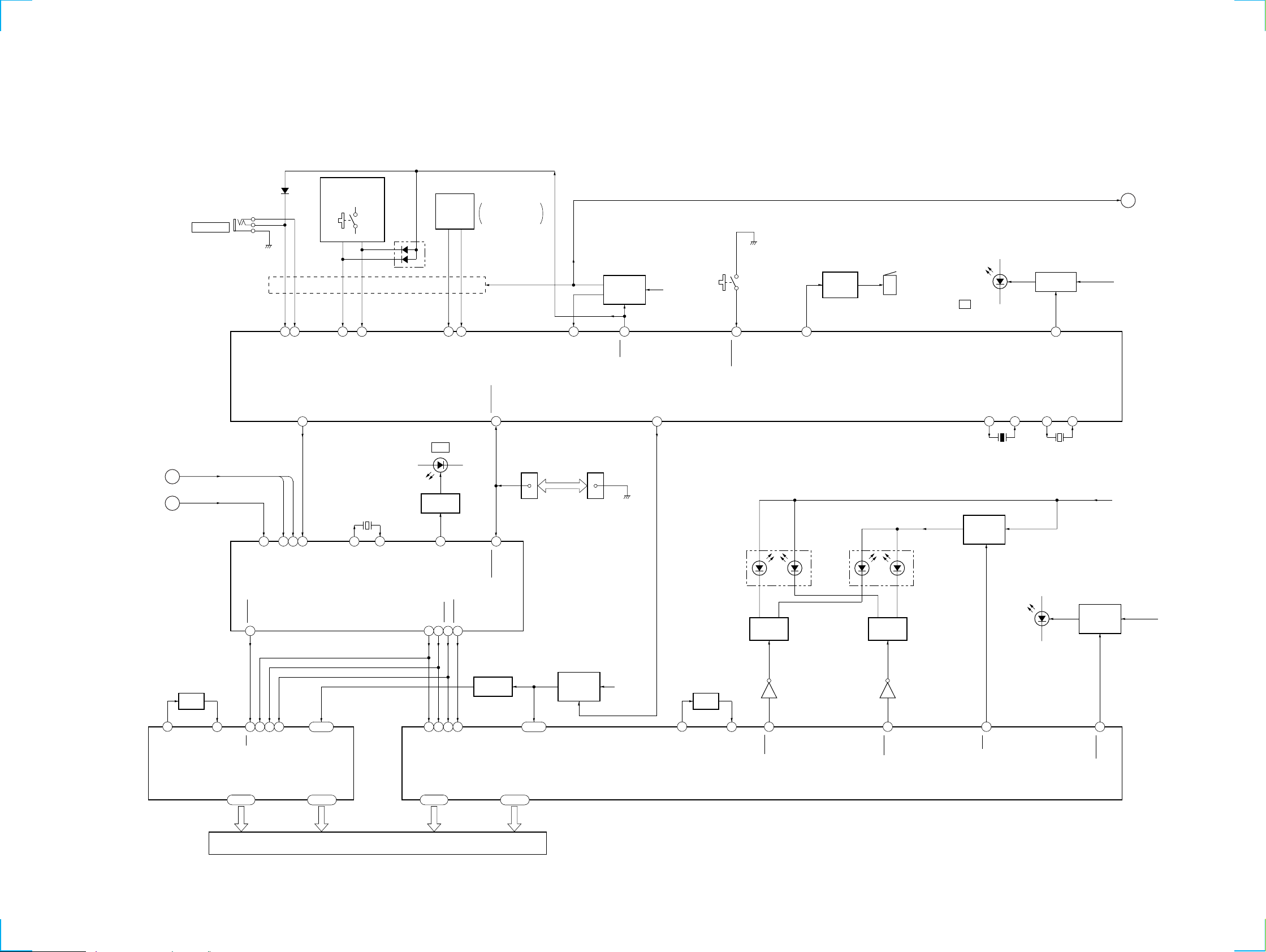
Page 25
5-5. BLOCK DIAGRAM – BUS CONTROL/POWER SUPPLY Section –
RST
DATA IN
DATA OUT
CLK IN
BUS
ON IN
BU IN
REMOTE CONTROL
RECEIVER
IC910
13
9
8
11
12
10
SIRCS
BUFFER
Q275
D204
LEVEL SHIFT
IC702
(Page 23)
SIRCS
RESET
DATA
CLK
BUS ON
BATT
CN271
BUS CONTROL IN
(FOR SONY BUS)
BATT B+
(Page 23)
H
3
2
5
4
6
7
G
POW-ON
RESET
BACKUP +5V
BUS ON SWITCH
Q272
TH271
RESET SIGNAL
GENERATOR
BUS-ON
IC506
2
6
4
1
3
D276
D275
S703
RESET
SONY BUS INTERFACE
IC271
RST
RESET
SWITCH
DATA
CLK
BUS ON
OUT
BUS ON
SWITCH
BATT
BATTERY
SWITCH
BATTERY
DETECT
Q271
LEVEL SHIFT
Q274
LEVEL SHIFT
Q273
MASTER CONTROLLER
IC500 (4/4)
SIRCS
24
RESET
90
86
HSTX
6
SYSRST
UNISO
21
20
UNISI
22
UNICKO
7
BUS-ON
BU-IN
77
LIQUID CRYSTAL DISPLAY
DRIVE CONTROLLER
82
NMI (H)
49
BU-IN
BUS-ON
38
81
RESET
101
UNICKI
UNISI
98
UNISO
97
MD MECHANISM CONTROLLER
60
BU-IN
BUS-ON
61
30
RESET
48
UNICKIO
49
UNISI
UNISO
50
46
LINKOFF
CSV ON 16
DSP ON
SHIFT OUT
PWM IN 65
ACC IN
ILL IN
FM-ON
TU-ON
IC701 (2/2)
IC501 (2/2)
MDMON
114
MDX-C8970R
CNP401 (2/2)
(POWER CONNECTOR)
F1
BATT B+
PULL UP +5V
BACKUP +5V
+5V
(CSV CIRCUIT B+)
3
14
2
+3.3V
+3.3V REGULATOR
IC404
+3.3V REGULATOR
IC401, Q401
IN1
ERROR
AMP
IN2
ERROR
AMP
RT
B+ SWITCH
Q901
FM-ON
OSC
REGULATOR
IC401, Q401
B+ SWITCH
Q183
COMPARATOR
COMPARATOR
+3.3V
VCC
Q182
DIG +3.3V
(DSP CIRCUIT B+)
96
72
61
85
84
52ILL-ON
(RDS DECODER (IC901) B+)
65MD-ON
10
ACC IN
ILL IN
ANA +3.3V
DSP +5V
OSC SWITCH
Q890
LOAD +12V
LOADING MOTOR
DRIVER (IC305) B+
DRIVER +5V
MOTOR/COIL DRIVER
(IC303) B+
TU +8V
(TUNER CIRCUIT B+)
TU +5V
(TUNER CIRCUIT B+)
+5V
FM +8V
(FM CIRCUIT B+)
AM +8V
(AM CIRCUIT B+)
B+ SWITCH
Q801, 802
B+ SWITCH
Q402, 403
PWN
PWN
POWER CONTROL
IC871
B+ SWITCH
Q402, 403
+5V
REGULATOR
Q185
B+ SWITCH
Q180
Q181
OUTPUT
CIRCUIT
OUTPUT
CIRCUIT
OUT1
OUT2
VCC
7
10
9
B+ SWITCH
Q886,887
+8V
REGULATOR
IC403
TU-ON
LCD DRIVER (IC900, 920)/
ILLUMINATION LED B+
D424
D422
D403
AUDIO +8.5V
(AUDIO CIRCUIT B+)
+5V
(MIC AMP CIRCUIT B+)
LCD +10V
ACCESSORY CHECK
Q441
POWER AMP
(IC481) B+
B+ CHECK
IC421
SWITCHING
REGULATOR
Q884
POWER
CONTROL SWITCH
Q882
ANTENNA REMOTE
Q461(2/2), 462(2/2)
+5V
REGULATOR
Q841
B+ SWITCH
Q253, 256
ILL-ON
SWITCH
D442
REGULATOR
Q421, 422
REGULATOR
CONTROL SWITCH
Q423, 424
SWITCHING
REGULATOR
B+ SWITCH
AMP REMOTE
SWITCH
Q461(1/2), 462(1/2)
REGULATOR
ILLUMINATION
LINE DETECT
Q431
+5V
Q883
Q881
TH461
TH462
POW-ON
TU-ON
BUS-ON
+8.5V
IC402
POW-ON
D431
16
14
5
6
7
BATT
AMP REM
ANT REM
ACC
ILL
05
2525
Page 26
d
5-6. NOTE FOR PRINTED WIRING BOARDS AND SCHEMATIC DIAGRAMS
(In addition to this, the necessary note is printed in each block)
• Circuit Boards Location
Note on Printed Wiring Boards:
• X : parts extracted from the component side.
• Y : parts extracted from the conductor side.
r
•
•
• b : Pattern from the side which enables seeing.
(The other layers' patterns are not indicated.)
Caution:
Pattern face side: Parts on the pattern face side seen from
(Conductor Side) the pattern face are indicated.
Parts face side: Parts on the parts face side seen from
(Component Side) the parts face are indicated.
: Through hole.
¢
: internal component.
Note on Schematic Diagram:
• All capacitors are in µF unless otherwise noted. pF: µµF
50 WV or less are not indicated except for electrolytics
and tantalums.
• All resistors are in Ω and 1/
specified.
¢
•
• C : panel designation.
Note: The components identified by mark ! or dotted line
• U : B+ Line.
• H : adjustment for repair.
• Power v oltage is dc 14.4V and fed with regulated dc pow er
• Voltages are tak en with a V OM (Input impedance 10 MΩ).
• Waveforms are taken with a oscilloscope.
• Circled numbers refer to waveforms.
• Signal path.
• Abbreviation
: internal component.
with mark ! are critical for safety.
Replace only with part number specified.
supply from ACC and BATT cords.
Voltage variations may be noted due to normal produc-
tion tolerances.
Voltage variations may be noted due to normal produc-
tion tolerances.
F : FM
f : MW/LW
E : MD
TYPE A : ENGLISH, SPANISH
TYPE B : ENGLISH, GERMAN
TYPE C : ENGLISH, FRENCH
4
W or less unless otherwise
RELAY board
DISPLAY board
MAIN board
SENSOR board
SERVO board
POWER boar
26
26
Page 27
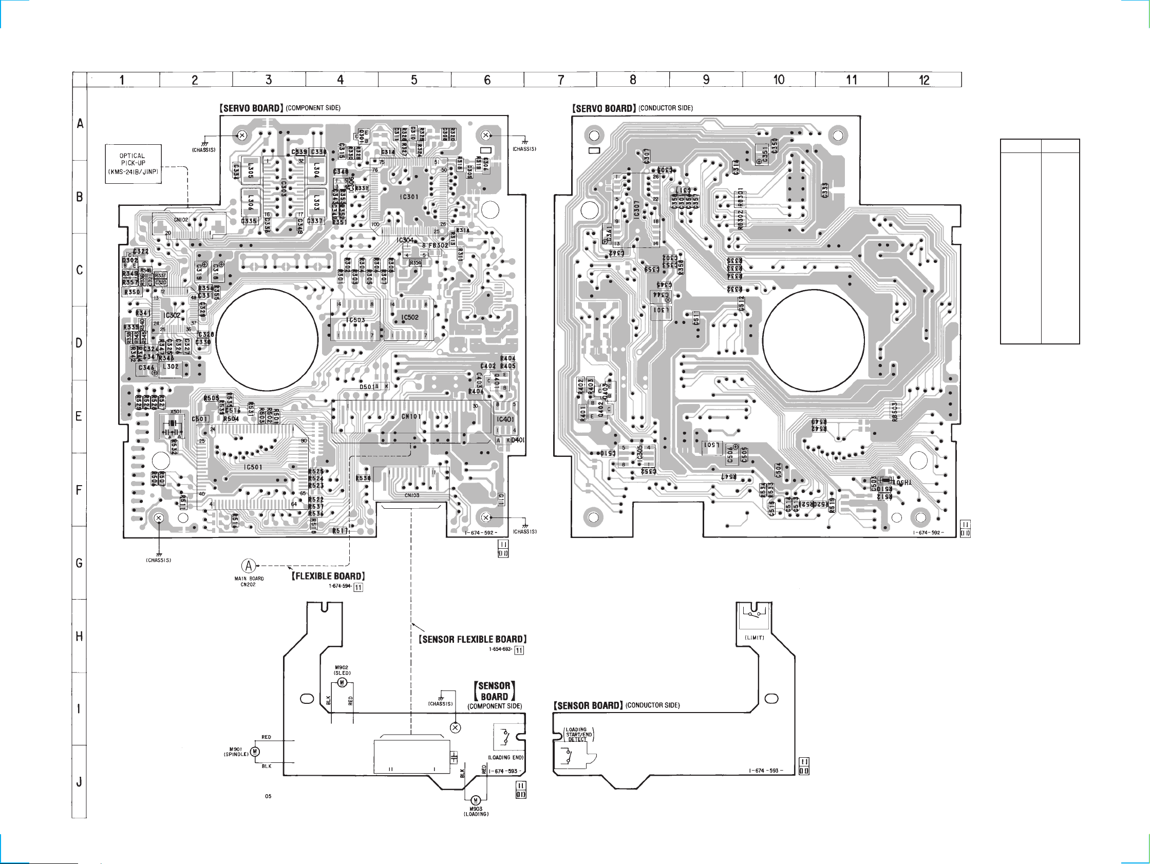
5-7. PRINTED WIRING BOARD – SERVO/SENSOR Boards – • See page 26 for Circuit Boards Location.
MDX-C8970R
• Semiconductor
Location
Ref. No. Location
D401 E-6
D501 E-5
IC301 B-5
IC302 D-2
IC303 B-3
IC304 C-5
IC305 F-8
IC306 B-4
IC307 B-8
IC401 E-6
IC501 F-3
IC502 D-5
IC503 D-4
Q301 A-4
Q302 C-1
Q401 E-6
Q402 E-8
Q403 E-8
(Page 30)
2727
Page 28
MDX-C8970R
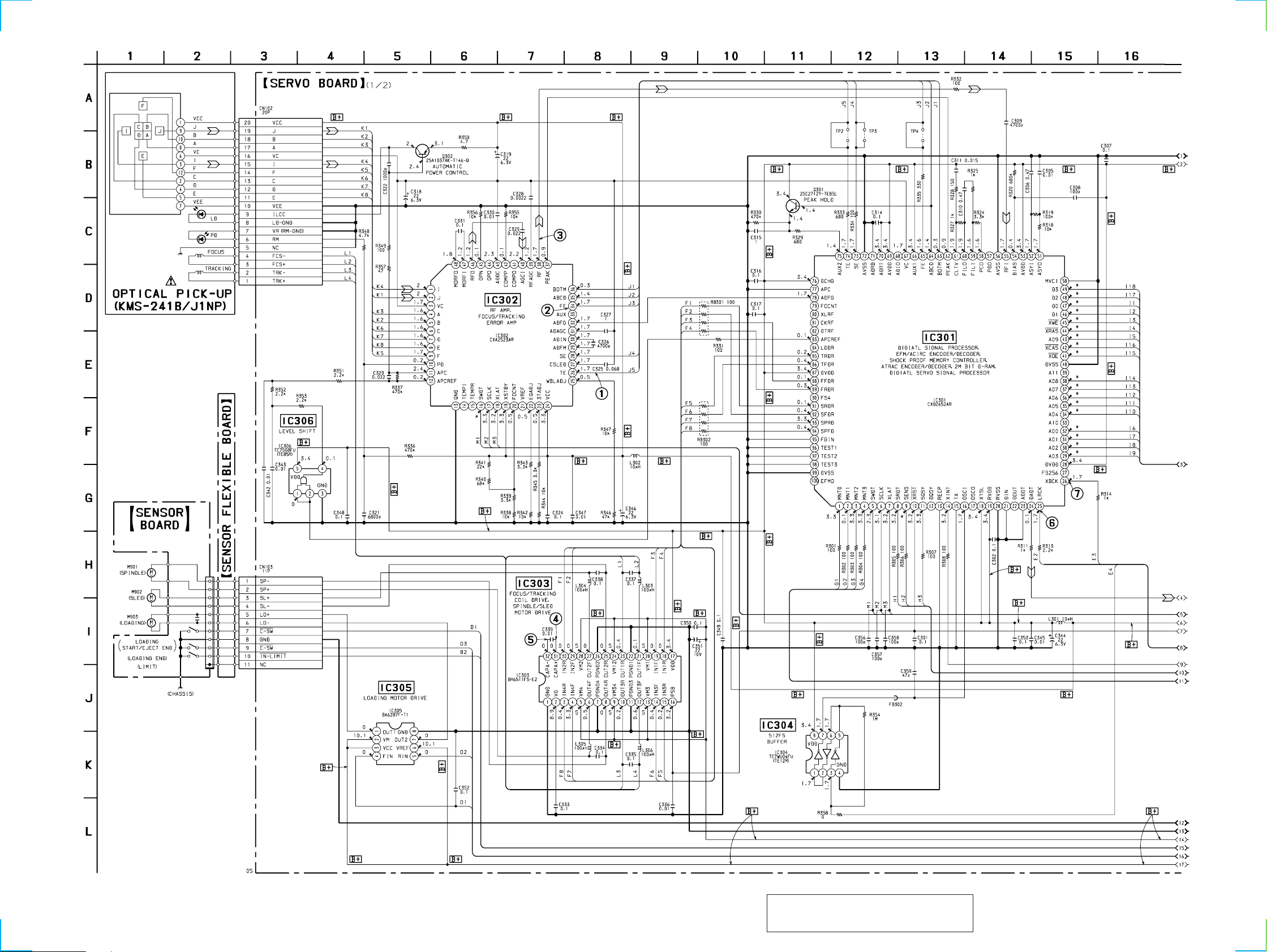
5-8. SCHEMATIC DIAGRAM – SERVO (1/2)/SENSOR Boards – • See page 37 for Waveforms. • See page 44 for IC Block Diagrams.
28
28
The components identified by mark ! or dotted
line with mark ! are critical for safety.
Replace only with part number specified.
Note on Schematic Diagram:
• Voltages and waveforms are dc with respect to
ground in playback mode.
no mark : MD
: Impossible to measure
∗
Page 29
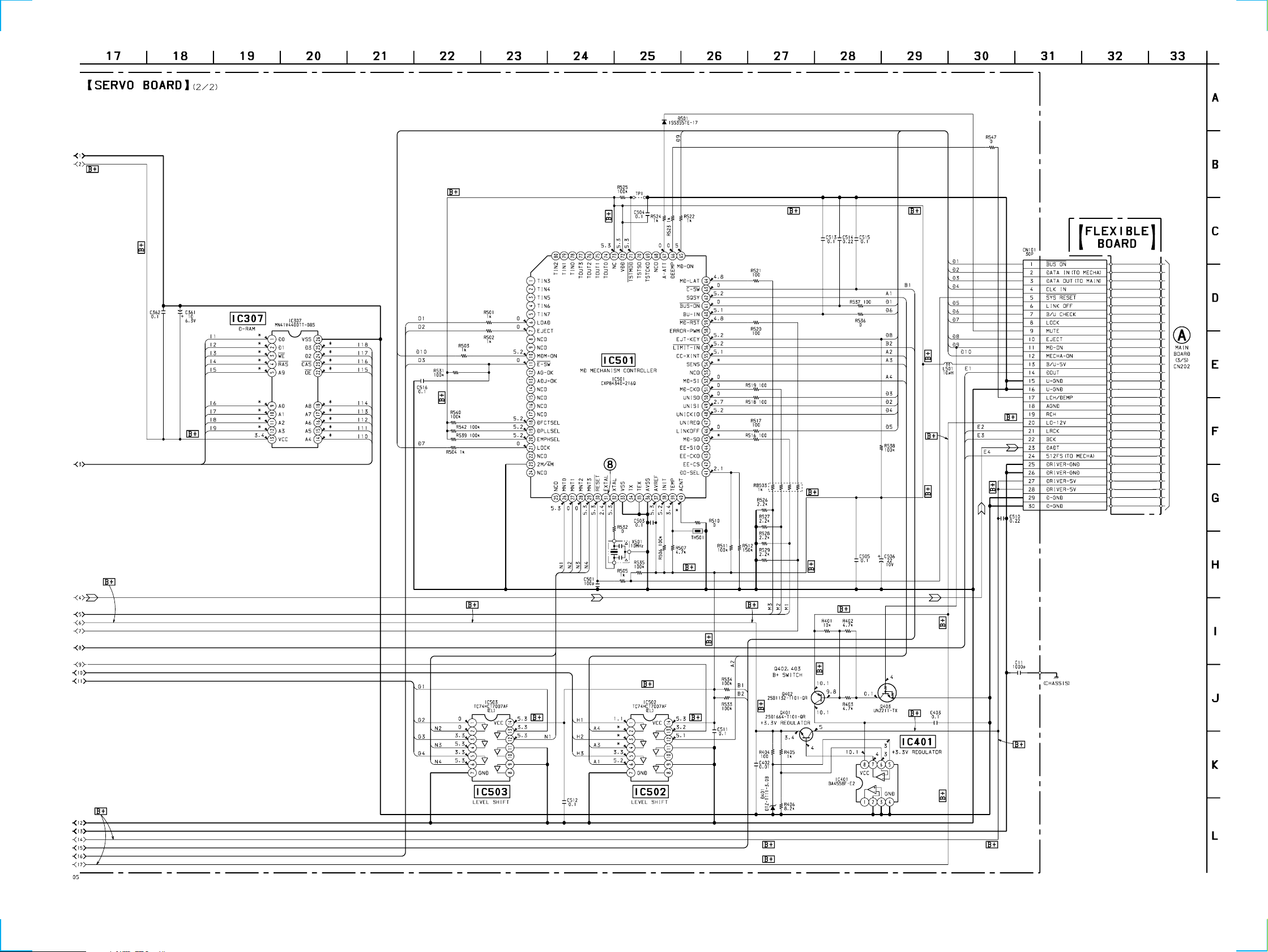
5-9. SCHEMATIC DIAGRAM – SERVO Board (2/2) – • See page 37 for Waveforms. • See page 46 for IC Block Diagrams.
MDX-C8970R
(Page
34)
2929
Page 30
MDX-C8970R
• Semiconductor Location
5-10. PRINTED WIRING BOARD – MAIN Board (Component Side) – • See page 26 for Circuit Boards Location.
Ref. No. Location
D131 J-2
D2O4 J-11
D251 K-12
D252 K-12
D253 K-12
D254 K-11
D255 K-13
D256 K-13
D257 K-12
D258 K-12
D259 K-12
D260 K-12
D261 K-13
D262 K-11
D263 K-11
D264 K-11
D265 K-11
D271 D-13
D279 B-14
D280 A-14
D282 A-14
D283 B-13
D291 B-13
D421 E-11
D422 E-12
D423 D-12
D424 D-12
D441 E-9
D442 E-9
D461 C-10
D462 C-10
D463 C-10
D464 C-9
D466 C-9
D471 C-8
D472 D-8
D481 B-7
D482 B-7
D483 B-6
D484 B-6
D485 B-7
D486 B-8
D487 B-8
D488 B-8
D491 B-6
D546 K-3
D601 B-5
D631 B-4
D661 A-1
D701 H-11
IC151 E-3
Ref. No. Location
IC271 C-13
IC300 H-6
IC404 E-10
IC421 E12
IC500 J-6
IC506 H-5
IC602 D-7
IC632 D-6
IC691 G-8
IC701 H-12
IC702 J-11
IC901 J-3
IC951 H-3
IC952 I-3
Q130 I-2
Q131 I-2
Q132 I-2
Q133 G-1
Q134 I-2
Q180 B-2
Q181 B-2
Q182 C-2
Q183 C-2
Q185 D-3
Q251 J-9
Q252 J-10
Q253 I-9
Q254 J-10
Q255 J-9
Q256 J-9
Q271 C-13
Q272 C-12
Q275 B-13
Q421 D-11
Q422 D-11
Q423 E-11
Q424 E-11
Q441 F-9
Q451 D-10
Q461 D-9
Q462 E-10
Q471 C-8
Q472 D-8
Q473 C-8
Q474 D-8
Q501 H-5
Q523 J-8
Q691 G-8
Q751 F-2
Q752 G-2
Q754 F-2
s
s
s
s
(Page
38)
30
(Page 27)
30
Page 31

5-11. PRINTED WIRING BOARD – MAIN Board (Conductor Side) – • See page 26 for Circuit Boards Location.
MDX-C8970R
(Page 42)
• Semiconductor Location
Ref. No. Location
IC604 C-6
IC631 F-6
IC633 D-6
IC634 C-4
IC661 E-5
IC663 B-2
IC752 G-2
IC771 F-3
Q273 B-13
Q274 B-13
Q401 F-9
Q402 F-12
Q403 F-10
Q431 D-8
Q504 J-5
Q601 B-5
Q602 B-5
Q631 B-4
Q632 B-4
Q661 B-2
Q662 A-2
Q753 F-2
Q901 J-2
JC103
Ref. No. Location
D181 C-2
D272 B-12
D273 B-12
D274 B-12
D275 C-12
D276 B-12
D277 B-13
D278 B-13
D403 F-13
D431 D-9
D432 D-9
D477 B-13
D489 A-7
D527 I-9
D555 J-7
D702 I-12
D751 F-2
IC351 H-6
IC401 E-9
IC402 E-10
IC403 D-10
IC481 A-7
IC601 F-7
IC603 D-7
3131
Page 32

MDX-C8970R
5-12. SCHEMATIC DIAGRAM – MAIN Board (1/5) – • See page 37 for Waveforms. • See page 48 for IC Block Diagrams.
(Page 36)
(Page 33)
Note on Schematic Diagram:
• Voltages and waveforms are dc with respect to ground
under no-signal (detuned) conditions.
no mark : FM
(Page 34)
32
(Page 35)
32
Page 33

5-13. SCHEMATIC DIAGRAM – MAIN Board (2/5) – • See page 47 for IC Block Diagrams.
MDX-C8970R
(Page
32)
(Page 34)
(Page 35)
3333
Note on Schematic Diagram:
• Voltages and wavefor ms are dc with respect to ground
under no-signal (detuned) conditions.
no mark : FM
Page 34

MDX-C8970R
5-14. SCHEMATIC DIAGRAM – MAIN Board (3/5) – • See page 37 for Waveforms.
(Page 32)
(Page
36)
(Page 33)
(Page
29)
(Page
35)
(Page 36)
34
34
Note on Schematic Diagram:
• V oltages and wa veforms are dc with respect to ground
under no-signal (detuned) conditions.
no mark : FM
( ) : MW
[]: LW
〈〈 〉〉 : MD PLAY
Page 35

5-15. SCHEMATIC DIAGRAM – MAIN Board (4/5) – • See page 47 for IC Block Diagrams.
(Page 32)
MDX-C8970R
(Page 33)
(Page
38)
(Page
34)
(Page 43)
(Page 39)
Note on Schematic Diagram:
• Voltages and waveforms are dc with respect to ground
under no-signal (detuned) conditions.
no mark : FM
〈〈 〉〉 : MD PLAY
3535
Page 36

MDX-C8970R
5-16. SCHEMATIC DIAGRAM – MAIN Board (5/5) – • See page 37 for Waveforms. • See page 47 for IC Block Diagrams.
(Page
34)
36
(Page
32)
Note on Schematic Diagram:
• V oltages and waveforms are dc with respect to ground
under no-signal (detuned) conditions.
no mark : FM
( ) : MW
[]: LW
〈〈 〉〉 : MD PLAY
36
Page 37

• Wavef orms
14.8 Vp-p
3.9 µs
2.6 Vp-p
69.8 ns
1.4 Vp-p
5.8 µs
– SERVO Board –
– MAIN Board –
– POWER Board –
1 IC302 @§ (TE) (MD PLAY)
2 IC302 #¢ (FE) (MD PLAY)
3 IC302 #• (RF) (MD PLAY)
Approx.
0.5 Vp-p
Approx.
0.3 Vp-p
6 IC301 @∞ (LRCK) (MD PLAY)
22.6 µs
7 IC301 @§ (XBCK) (MD PLAY)
180 ns
8 IC501 #¡ (EXTAL) (MD PLAY)
3.9 Vp-p
4.4 Vp-p
1 IC300 $¡ (XTLI38)
59 ns
2 IC300 &∞ (BCK)
354 ns
3 IC300 &§ (LRCK)
1.5 Vp-p
4.4 Vp-p
6 IC151 9 (OSCI)
98 ns
7 IC951 $¶ (XT)
239 ns
8 IC901 5 (OSC1)
2.2 Vp-p
4.1 Vp-p
1 Q833 5 to 8 (D)
2 Q883 4 (GATE)
11.6 Vp-p
3.9 µs
3 IC801@º (XI1)
4 IC303 #¡ (CAPA+) (MD PLAY)
20 ns
5 IC303 #™ (CAPA–) (MD PLAY)
1.3 Vp-p
4.4 Vp-p
4.4 Vp-p
100 ns
26.8 mVp-p
22.7 µs
4 IC500 &¢ (X0A)
30.5 µs
5 IC500 (™ (X0)
4.4 Vp-p
2.5 Vp-p
4.7 Vp-p
231 ns
9 IC701 *§ (EXTAL)
54.3 ns
1.7 Vp-p
3.9 Vp-p
– DISPLAY Board –
1 IC900 @º (OSC-IN)
1.8 Vp-p
4.9 µs
2 IC920 !™ (OSC-IN)
40 ns
279 ns
3737
Page 38

MDX-C8970R
5-17. PRINTED WIRING BOARD – POWER Board – • See page 26 for Circuit Boards Location.
• Semiconductor
Location
(Component Side)
Ref. No. Location
D841 B-6
D871 C-8
D872 A-8
IC802 A-3
IC803 B-1
IC804 A-4
IC805 C-2
IC871 C-8
Q801 B-4
Q802 B-4
Q841 A-6
Q881 B-8
Q882 B-8
Q884 C-8
Q886 B-7
Q887 B-7
• Semiconductor
Location
(Conductor Side)
Ref. No. Location
D842 A-6
D891 C-4
D892 C-4
IC801 B-2
IC841 B-5
IC843 A-5
Q883 A-8
Q890 C-7
(Page 30)
38
38
Page 39

5-18. SCHEMATIC DIAGRAM – POWER Board – • See page 37 for Waveforms. • See page 50 for IC Block Diagrams.
(Page
35)
MDX-C8970R
Note on Schematic Diagram:
• Voltages and wavefor ms are dc with respect to ground
under no-signal (detuned) conditions.
3939
no mark : FM
Page 40

MDX-C8970R
• Semiconductor
Location
(Component Side)
Ref. No. Location
IC910 C-4
LED900 C-4
LED901 B-4
LED902 A-3
LED903 A-2
LED904 C-2
LED905 C-2
LED906 B-2
LED907 B-2
LED971 A-5
LED972 B-5
LED973 C-12
LED974 C-5
LED975 A-12
LED976 B-12
5-19. PRINTED WIRING BOARD – DISPLAY Board – • See page 26 for Circuit Boards Location.
• Semiconductor
Location
(Conductor Side)
Ref. No. Location
D901 B-5
D902 B-4
D903 A-8
D905 B-8
D971 B-4
IC900 B-6
IC920 B-9
IC921 B-8
Q900 B-5
Q901 B-5
Q902 A-5
Q903 A-5
Q904 B-4
Q971 B-4
Q972 B-4
(Page 42)
40
40
Page 41

5-20. SCHEMATIC DIAGRAM – DISPLAY Board – • See page 37 for Waveforms.
(Page
43)
MDX-C8970R
Note on Schematic Diagram:
• Voltages and waveforms are dc with respect to ground
under no-signal (detuned) conditions.
no mark : FM
4141
Page 42

MDX-C8970R
5-21. PRINTED WIRING BOARD – RELAY Board – • See page 26 for Circuit Boards Location.
(Page 31)
42
(Page 40)
42
Page 43

5-22. SCHEMATIC DIAGRAM – RELAY Board –
MDX-C8970R
(Page 41)
(Page 35)
43
Page 44

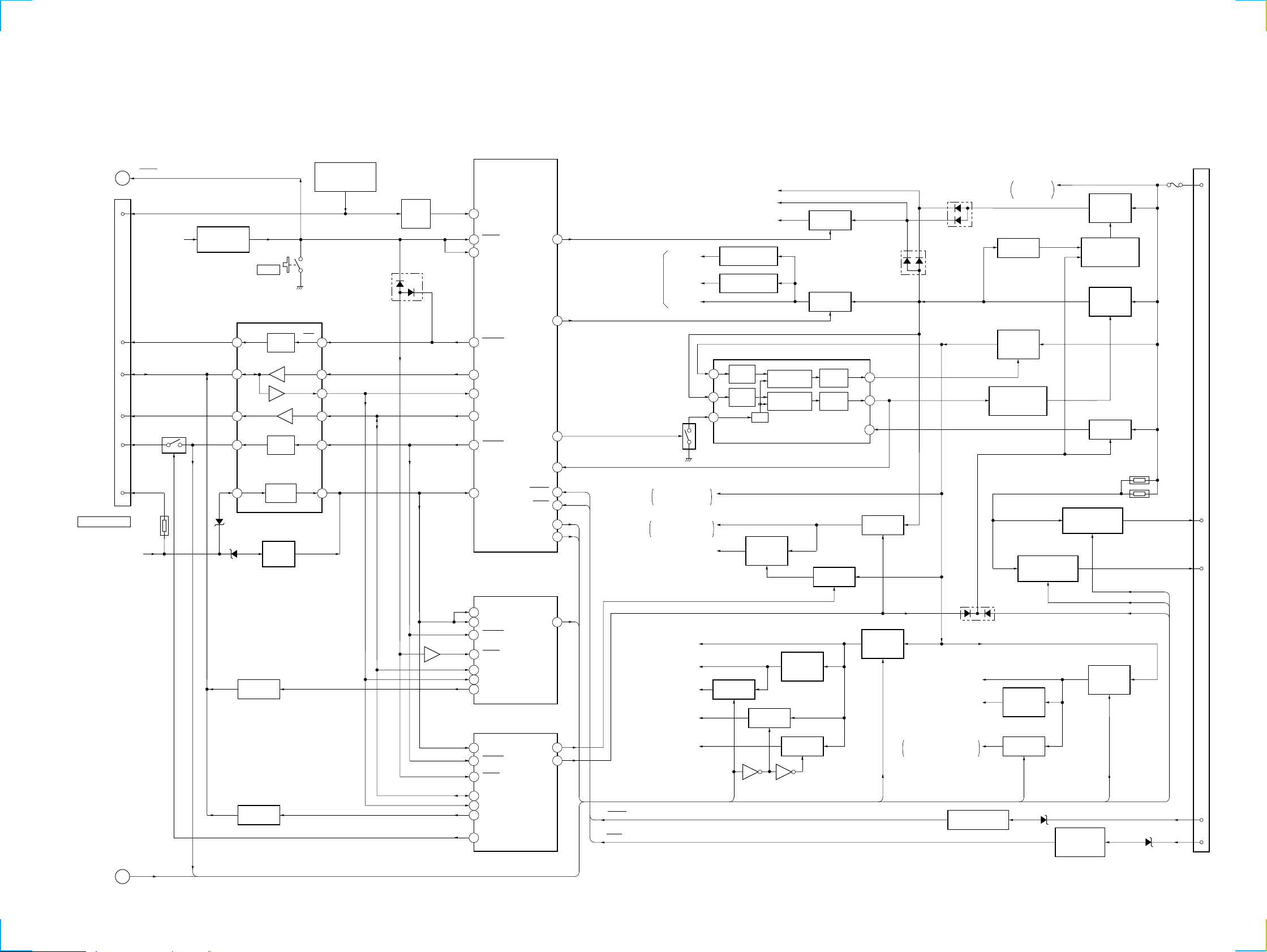
• IC Block Diagrams
– SERVO Board –
IC301 CXD2652AR
EFMO
DVSS
TEST3
TEST2
99 98 97 96 95 94 93
EACH
BLOCK
EACH
BLOCK
SUBCODE
CLOCK
MNT0
MNT1
MNT2
MNT3
SWDT
SCLK
XLAT
SRDT
SENS
XRST
SQSY
DQSY
RECP
XINT
OSCI
OSCO
XTSL
DVSS
DIN
DOUT
100
1
2
MONITOR
CONTROL
3
4
5
6
CPU I/F
7
8
9
10
11
PROCESSOR
12
13
14
15
TX
16
17
GENERATOR
18
19
NC
20
21
22
TEST1
FGIN
SPINDLE
SERVO
DECODER
EACH
BLOCK
SPFD
ADIP
SPRD
DIGITAL
AUDIO
SFDR91SRDR90FS489FRDR88FFDR87DVDD86TFDR85TRDR84LDDR83APCREF82DTRF81CKRF80XLRF79F0CNT78ADFG77APC76DCHG
92
PWM
SHOCK RESISTANT
MEMORY CONTROLLER
SAMPLING
I/F
RATE
CONVERTER
GENERATOR
SERVO
DSP
CONVERTER
AUTO
SEQUENCER
A/D
ANALOG
DECODER
ENCODER/
EFM/ACIRC
COMP
MUX
PLL
75
AUX2
74
TE
73
SE
72
AVSS
71
ADRB
70
ADRT
69
AVDD
68
ADIO
67
VC
66
AUX1
65
FE
64
ABCD
63
BOTM
62
PEAK
61
CLTV
60
FILO
59
FILI
58
PCO
57
PDO
56
AVSS
55
RFI
54
BIAS
53
AVDD
52
ASYI
51
ASYO
ADDT
DADT
LRCK
23
24
25
28
26
27
XBCK
DVDD
FS256
ATRAC
ENCODER/DECODER
ADDRESS/DATA BUS A00 - A11, D0 - D3
40
39
A1138A0837A0736A0635A0534A0433A1032A0031A0130A0229A03
41
DVSS
XOE
42
43
XCAS
A09
44
XRAS
XWE
50
49D348D247D046D145
MVCI
44
Page 45

IC302 CXA2523AR
MORFO47MORFI46RFO45OPN
48
–
+
RFA1
+
–
AA
BB
CC
DD
EE
FF
–
1
–
–
2
–
–
1
–
2
–
GRVA
EBAL
RFA2
OFST
+
–
+
–
FBAL
HLPT
GRV
1I
2J
CVB
3VC
4A
IVR
5B
IVR
6C
IVR
7D
IVR
8E
IVR
9F
IVR
GSW
+
–
+
–
+
–
+
–
+
–
+
–
+
–
IV
OPO43ADDC42COMPP41COMPO40AGCI39RF AGC38RF37PEAK
44
USROP
EE'
–1
–2
–2
–1
–
–
–
–
+
+
–
–
–
–
+
+
ESW
FF'
–
+
–
+
BPF3T
BPF22
WBL
WBL
RFA3
PTGR
PBSW
ABCDA
FEA
ATA
EFB TESW
RF AGC EQ
+
–
USRC
3T
3T WBL
PEAK
BOTTOM
WBL
ADIP
AGC
PTGR
WBL
EQ
PEAK3T
P-P
PBH
3T
DET
–1
–2
–1
–2
TEMP
DET
EQ
AUX
SW
BPFC
SEA
TEA
VI CONV
TG
TG
36
BOTM
35
ABCD
34
FE
33
AUX
32 ADFG
31 ADAGC
30 ADIN
29 ADFM
28 SE
27 CSLED
26 TE
25 WBLADJ
15
AUXSW
TEMPR
COMMAND
SCRI - PARA
DECODE
17
16
SCLK
SWDT
BGR
VREF
24
23
22
21
20
19
18
XLAT
XSTBY
F0CNT
VREF
EQADJ
3TADJ
VCC
10PD
11APC
12APCREF
+
–
+
–
14
13
GND
TEMPI
45
Page 46

IC303 BH6511FS-E2
CAPA–
CAPA+
IN2R
IN2F
VM2
OUT2F
PGND2
OUT2R
VM12
OUT1R
PGND1
OUT1F
VM1
32 31 30 29 28 27 26 25 24 23 22 21 20 19 18 17
IN4F
AMP
AMP
VM4
INTERFACE
CHARGE
PUMP.
OSC
INTERFACE
1 2 3 4 5 6 7 8 9 10 11 12 13 14 15 16
VG
GND
IN4R
OUT4F
AMP
PGND4
OUT4R
VM34
AMP
OUT3R
PGND3
AMP
AMPAMPAMP
OUT3F
PREDRIVEPREDRIVE
PREDRIVEPREDRIVE
VM3
IC305 BA6287F-T1
OUT1
1
GND
8
IN1F
INTERFACE
INTERFACE
IN3F
IN1R
IN3R
V
PSB
DD
V
DD
PSB
VM
2
DRIVER DRIVER
TSD
VCC
3
POWER
SAVE
FIN
4
CONTROL LOGIC
IC307 MN41V4400TT-08S
TIMING
GENERATOR
DQ1
1
2
DQ2
3
WE
4
RAS
5
A9
NC
6
7
NC
8
NC
9
A0
10
A1
11
A2
12
A3
ADDRESS BUFFERS
COLUMN
ROW
INTERNAL
ADDRESS
COUNTER
ROW
DECODERS
REFRESH
CONTROL
CLOCK
WORD
DRIVERS
OUT2
7
VREF
6
RIN
5
COLUMN
DECODERS
SENSE
AMPLIFIERS
MEMORY
CELLS
TIMING
GENERATOR
I/O
SELECTOR
INPUT
BUFFERS
DATA BUS
WRITE
CLOCK
GENERATOR
OUTPUT
BUFFERS
VSS
26
25
DQ4
DQ3
24
23
CAS
22
OE
NC
21
20
NC
NC
19
A8
18
A7
17
16
A6
A5
15
A4
14
VCC
46
13
Page 47

– MAIN Board –
IC151 TDA7427ADTR
LP OUT
11 BIT
PROGRAMMABLE
COUNTER
SWITCH
OUT
INLOCK
CHARGE
PUMP
DETECTOR
PARATOR
+
–
SWITCH
LP1/LP2
3 41 2 7
VREF
LP HC
LP FM
LP AM
PHASE
COM-
SWITCH
SWM/DIR
5 BIT
PROGRAMMABLE
COUNTER
PRE
COUNTER
SWITCH
SWM/DIR
16 BIT
PROGRAMMABLE
COUNTER
TEST
LOGIC
PORT
EXTENSION
5 6 11 129
DOUT3
DOUT4
DOUT5
8
DOUT6
FM/AM
SWITCH
TIMER
14 BIT
PROGRAMMABLE
COUNTER
REFERENCE
OSCILLATOR
10
OSCIN
OSCOUT
VDD2
AM IN
GND-AM
NC
NC
FM IN
POWER ON RESET
11 – 21 BIT
PROGRAMMABLE
GND-SIG
SUPPLY &
CONTROL
COUNTER
VDD1
ADDR
IIC BUS
INTERFACE
13 14
SCL
HFREF
SDA
DOUT1/INLOCK
SSTOP
DOUT2
1516171819202122232425262728
FM/AM
SWITCH
IF FM
IF AM
IC271 BA8270FV-E2
BUS ON
1
2
RST
BATT
3
4
CLK
5
VREF
6
DATA
GND
7 8
BUS ON
SWITCH
RESET
SWITCH
BATTERY
SWITCH
14
13
12
11
10
9
VCC
RST
BUS ON
CLK IN
BU IN
DATA IN
DATA OUT
IC602, 632 LM1973MX
IN3
GND3
VSS1
OUT2
18
19
20 17 16
RESISTIVE
NETWORK
TAP
SWITCHES
DECODE
SWITCH
DRIVE
TAP
SWITCHES
RESISTIVE
NETWORK
1 2 3
IN2
GND2
GND AC
OUT3
DECODE
SWITCH
TAP
SWITCHES
RESISTIVE
NETWORK
4 5 6
IN1
GND1
VDD215GND AC14VDD113DATA-OUT12DATA-IN
SWITCH
DRIVE
DRIVE
OUT1
7
8
VSS2
DECODE
REGISTER
LOGIC GND
LATCH
SHIFT
9
CLOCK
10
11
LOAD/SHIFT
47
Page 48

IC300 CXD2727Q
XMST
VDD3
AVSP
XPLLEN
80 79 78 77 76 75 74 73 72 71 70 69 68 67 66 65 64 63 62 61 60 59 58 57 56 55 54 53 52 51
PLCLK
81
XECKSTP
82
AVDP
83
VSS4
84
T. P
85
T. P
86
T. P
87
T. P
88
T. P
89
T. P
90
T. P
91
T. P
92
T. P
93
T. P
94
VDD4
95
AVSD
96
T. P
97
T. P
98
T. P
99
AVDD
100
SIN
BCK
LRCK
SERIAL DATA
MICRO
COMPUTER
I/F
512kbit
DELAY
RAM
SI1
SI2
SI3
I/F
GENERATOR/
TIMING CIRCUIT
SOUT
DSP
CLOCK
PLL
SO3
SO2
SO1
RVDT
XS24
VDD2
VSS3
SERIAL
DATA
I/F
DIGITAL
FILTER
CLOCK
GENERATOR/
TIMING CIRCUIT
XLAT
TRDT
REDY
SCK
BFOT
XRST
ADC2
ADC1
DAC6
DAC5
DAC4
DAC3
DAC2
DAC1
VSS2
AVD6
AOUTL3
AVD4
AOUTR3
AVS4
50
AVS6
49
AVD2
48
AVS2
47
RREF
46
RIN
45
AVS8
44
AVD8
43
AOUTR2
42
AVSX
41
–
+
–
+
–
+
–
+
–
+
–
+
40
39
38
37
36
35
34
33
32
31
XTLI38
XTLO38
AVDX
AOUTL2
AVD7
AVS7
LIN
LREF
AVS1
AVD1
AVS5
1 2 3 4 5 6 7 8 9 10 11 12 13 14 15 16 17 18 19 20 21 22 23 24 25 26 27 28 29 30
T. P
T. P
T. P
VSS1
T. P
IC604, 634 NJM2160AM-TE2
1
VCCL
2
INL
SVRL
INML
INMR
SVRR
INR
BUFFER
3
BUFFER
REFERENCE
4
5
REFERENCE
6
7
BUFFER
BUFFER
VCCL
VCCL
VCCR
VCCR
T. P
LIFT
AMP
SIGNAL
AMP
SIGNAL
AMP
LIFT
AMP
T. P
T. P
T. P
T. P
T. P
16
15
14
13
12
11
10
T. P
T. P
T. P
T. P
TST0
TST1
TST2
TST3
TST4
TST5
JPE1
JPE2
JPE3
VDD1
AVS3
AVD3
AOUTL1
AVD5
AOUTR1
IC901 SAA6588T-118
6
VSSD
VREF
17
SIGNAL QUALITY
CLOCK
DATA
87
DAVN
VDDD
MPX
DECODER
445
INTERFACE
REGISTER
VSSA
15
POWER SUPPLY
& RESET
LVIN
20
CL+
CL–
LGND
OUTL
OUTR
RGND
CR–
9
CR+
MULTI
PATH
DETECTOR
2
1
MRO
MPTH
CLOCKED
COMPARATOR
RDS/RDBS
DEMODULATOR
TEST
CONTROL
3
19
TCON
18
BAND-PASS FILTER
OSCILLATOR
& CLOCK
4 5
OSCO
57kHz
8th ORDER
RDS/RDBS
DECODER
OSCI
SCOUT
CIN
VDDA
14
CLOCK
DATA
IIC BUS SLAVE
TRANSCEIVER
9 10
1316
SDA
AFIN
DETECTOR
SCL
PAUSE
MAD
PSWN
11
12
VCCR
48
8
Page 49

IC951 MSM6688GS-2K
CEWRRD
RESET
5253545556
NAR
RWCK
MON
51 46
DVDDXTXT
WE
DROM
DI/0
CS4
43444547484950
BUSY
RPM
VPM
ACON
TEST
MCUM
TEST
TEST
TEST
ADIN
TIMING
CONTROLLER
LPF
FOUT
AOUT
1
D0
2
D1
3
D2
4
D3
5
6
7
8
9
10
CE
11
12
13
14
MCU I/F
STATUS
REGISTER
TEST
CIRCUIT
12BIT
ADC
15 16 17 18 19 20 21 22 23 24 25 26 27 28
TEST
ADDRESS
CONTROLLER
ANALYZER/
SYNTHESIZER
FIN
AMON
OSC
ADPCM
12BIT
CIRCUIT
AVDD
DVDD
DAC
SG
DATA
I/O
REGISTER
CONTROLLER
-
+
SG
SGC
LOUT
LINE
+
MOUT
-
MIN
42
CS3
41
CS2
40
CS1
39
SADX
SADY
38
37
TAS
36
SAS
35
PDWN
34
TEST
33
TEST
RSEL2
32
RSEL1
31
DGND
30
29
AGND
IC952 MSM6685JSDR1
TEST
RWCK
TEST
TEST
TEST
TEST
DIN
VSS
1
2
NC
3
4
5
9
10
11
NC
12
13
I/O CONTROL
WRITE CLOCK
GENERATOR
TIMING
GENERATOR
8,388,608DATA
REGISTER
COLUMN DECODER
COLUMN ADDRESS
COUNTER
ROW
DECODER
ADDRESS
MULTIPLEXER
REFRESH TIMER
REFRESH ADDRESS
COUNTER
ROW ADDRESS
COUNTER
ROW ADDRESS
REGISTER
26
VCC
25
RS/A
24
RFSH
SAD
23
22
SAS
18
TAS
CS
17
WE
16
DOUT
15
14
NC
49
Page 50

– POWER Board –
IC801 RSC-164
AIN1
AIN0
AGND
BUFOUT/PWM0
TEST/PWM1
AVDD
GND
DACOUT
BUFFER
DAC
ANALOG
CONTROL
ADC
49
SH
50
ADC
MUX
51
52
53
54
55
56
D7
57
D6
58
D5
59
D4
60
D3
61
D2
62
D1
63
D0
64
DATA BUS
XML
XMH
EXTERNAL MEMORY
INTERFACE
WRD
INTERNAL ROM
32 X 8 (HIGH)
INTERNAL ROM
32 X 8 (LOW)
RDD
WRC
ADDRESS BUS
RDC
GND
VDD
P00
INTERNAL BUS
INTERRUPT
LOGIC
SLEEP
POWER
CONTROL
WAKEUP LOGIC
(FROM PORT 0/1)
P01
PON
P02
P03
PORT 0
TIMING &
CONTROL
P04
P05
33343536373839404142434445464748
REGISTER
SPACE
PULSE WIDTH
MODULATOR
P06
STACK
SPACE
TIMER
CPU
OSC
PORT 1
32
P07
P10
31
P11
30
P12
29
P13
28
P14
27
P15
26
P16
25
P17
24
VDD
23
GND
22
RESET
21
XI1
20
XO1
19
18
A0
17
A1
1
A15
A14
A13
A12
62 3 54
87 9 1410 11 1312 16
A9
A8
A11
A10
GND
IC803 MSM534001E-49TSKFDR3 (TYPE C)
MSM534001E-50TSKFDR3 (TYPE A)
MSM534001E-51TSKFDR3 (TYPE B)
OE
A10CED7D6D5D4D3
32 2731 30 2829 2526 24 1923 22 2021 1718
ADDRESS
BUFFER
VSSD2D1D0A0A1A2
X
DECODER
Y
DECODER
CE/OE
CONTROL
MEMORY CELL
MATRIX
524,288 X 8
MULTIPLEXER
OUTPUT
BUFFER
A3
A7A6A5A4A3
VDD
15
A2
50
1 62 3 54
A9
A8
A11
A13
87 9 1410 11 1312 1615
A14
A17
A18
VCC
A7A6A5
NC
A16
A15
A12
A4
Page 51

IC805 MBM29F800TA
A16
A15
1
A14
2
A13
3
A12
4
A11
5
A10
6
A9
7
A8
8
9
NC
10
NC
WE
11
RESET
12
13
NC
NC
14
RY/BY
15
A18
16
A17
17
A7
18
A6
19
A5
20
A4
21
A3
22
A2
23
A1
24 25
ADDRESS
LATCH
STB
CONTROL
CIRCUIT
RY/BY
BUFFER
X
DECODER
Y
DECODER
8,388,608
CELL
MATRIX
Y GATE
DATA
LATCH
STB
LOW VCC
DETECTOR CIRCUIT
WRITE/ERASE
PULSE TIMER
WRITE CIRCUIT
ERASE CIRCUIT
CHIP ENABLE/
OUTPUT ENABLE
CIRCUIT
I/O
BUFFER
BYTE
GND
DQ15/A–1
DQ7
DQ14
DQ6
DQ13
DQ5
DQ12
DQ4
VCC
DQ11
DQ3
DQ10
DQ2
DQ9
DQ1
DQ8
DQ0
GND
OE
CE
A0
48
47
46
45
44
43
42
41
40
39
38
37
36
35
34
33
32
31
30
29
28
27
26
IC871 TL1451ACDB-E20
REF
OUT
S.C.P
NON-INV-
INPUT2
INV-
16 15 14 13 12
VERF.
+2.5V
VCC
REFERENCE
VOLTAGE
+2.5V
SHORT
CIRCUIT
PROTECTION
COMPARATOR
+
+
–
VREF/2
TRIANGLE
OSCILLATOR
2 3
1
CT
RT
INPUT2
–
+
ERROR
AMP2
VERF
SR R
LATCH
U.V.L.O
4
INV-
INPUT1
NON-INV-
VERF
+
–
INPUT1
FEED
BACK2
DEAD
11
VERF
ERROR
AMP1
5 6 7 8
FEED
DEAD
BACK1
TIME
CONTROL2
PWM
COMPARATOR2
PWM
COMPARATOR1
TIME
CONTROL1
OUT2
10
OUTPUT2
OUTPUT1
OUT1
VCC
9
GND
GND
51
Page 52

5-23. IC PIN FUNCTION DESCRIPTION
• MAIN BOARD IC300 CXD2727Q (DIGITAL SIGNAL PROCESSOR, DIGITAL FILTER, D/A CONVERTER)
Pin No. Pin Name I/O Description
1 VSS1 —
2 to 15 T.P
16 to 21 TST0 to TST5 I
22 to 24 JPE1 to JPE3 I
25 VDD1 —
26 AVS3 —
27 AOUTL1 O
28 AVD3 —
29 AOUTR1 O
30 AVD5 —
31 AVS5 —
32 AVD1 —
33 AVS1 —
34 LREF O
35 LIN I
36 AVS7 —
37
38 AOUTL2 O
39 AVDX —
40 XTLO38 O
41 XTLI38 I
42 AVSX
43 AOUTR2
44 AVD8
45 AVS8
46 RIN
47 RREF
48 AVS2
49 AVD2
50 AVS6
51 AVD6
52 AOUTL3
53 AVD4
54 AOUTR3
55 AVS4 —
56 VSS2 —
57 XRST I
58 BFOT O
AVD7
Ground terminal (digital system)
I Input terminal for the test (fixed at “L”)
Input terminal for the test (fixed at “L”)
External condition jump terminal “H”: condition jump (fixed at “L”)
Power supply terminal (+3.3V) (digital system)
Ground terminal (for D/A converter 1) (analog system)
D/A converter 1 (L-ch side) output terminal
Analog signal output for front side (L-ch side) output in this set
Power supply terminal (+3.3V) (for D/A converter 1) (analog system)
D/A converter 1 (R-ch side) output terminal
Analog signal output for rear side (L-ch side) output in this set
Power supply terminal (+3.3V) (for D/A converter 1) (analog system)
Ground terminal (for D/A converter 1) (analog system)
Power supply terminal (+3.3V) (for L-ch side A/D converter) (analog system)
Ground terminal (for L-ch side A/D converter) (analog system)
Connected to the bus control for A/D converter (for L-ch side)
A/D converter (L-ch side) analog input terminal
Tuner and bus audio input signal (L-ch side) in this set
Ground terminal (for D/A converter 2) (analog system)
—
Power supply terminal (+3.3V) (for D/A converter 2) (analog system)
D/A converter 2 (L-ch side) output terminal Not used (open)
Power supply terminal (+3.3V) (for master clock) (analog system)
System clock output terminal (16.9344 MHz)
System clock input terminal (16.9344 MHz)
— Ground terminal (for master clock) (analog system)
D/A converter 2 (R-ch side) output terminal
O
Analog signal output for sub woofer output in this set
— Power supply terminal (+3.3V) (for D/A converter 2) (analog system)
— Ground terminal (for D/A converter 2) (analog system)
A/D converter (R-ch side) analog input terminal
I
Tuner and bus audio input signal (R-ch side) in this set
O Connected to the bus control for A/D converter (for R-ch side)
— Ground terminal (for R-ch side A/D converter) (analog system)
— Power supply terminal (+3.3V) (for R-ch side A/D converter) (analog system)
— Ground terminal (for D/A converter 3) (analog system)
— Power supply terminal (+3.3V) (for D/A converter 3) (analog system)
D/A converter 3 (L-ch side) output terminal
O
Analog signal output for rear side (R-ch side) output in this set
— Power supply terminal (+3.3V) (for D/A converter 3) (analog system)
D/A converter 3 (R-ch side) output terminal
O
Analog signal output for front side (R-ch side) output in this set
Ground terminal (for D/A converter 3) (analog system)
Ground terminal (digital system)
System reset signal input from the master controller (IC500) “L”: reset
Master clock signal output terminal Not used (open)
52
Page 53

Pin No. Pin Name I/O Description
59 SCK I
60 REDY O
61 TRDT O
62 XLAT I
63 RVDT I
64 XS24 I
65 VDD2 —
66 VSS3 —
67 to 69 SO1 to SO3 O
70 SOUT O
71 SI1 I
72, 73 SI2, SI3 I
74 SIN I
75 BCK I
76 LRCK I
77 XMST I
78 VDD3 —
79 AVSP —
80 XPLLEN I
81 PLCLK O
82 XECKSTP I
83 AVDP —
84 VSS4 —
85 to 94 T.P
95 VDD4 —
96 AVSD —
97 to 99 T.P
100 AVDD —
Serial data transfer clock signal input from the master controller (IC500) and liquid crystal display
drive controller (IC701)
Transfer enable signal output to the master controller (IC500)
“L”: transfer prohibition
Serial data output to the master controller (IC500) and liquid crystal display drive controller
(IC701)
Serial data latch pulse input from the master controller (IC500)
Serial data input from the master controller (IC500)
Serial data 24/32 bit slot selection signal input terminal
“L”: 24 bit slot, “H”: 32 bit slot (validity at slave mode) (fixed at “H” in this set)
Power supply terminal (+3.3V) (digital system)
Ground terminal (digital system)
Serial data output terminal Not used (open)
Serial data output terminal Not used (open)
Serial data input from the CXD2652AR (IC301)
Serial data input terminal Not used (open)
Serial data input terminal Not used (open)
Bit clock signal (2.8224 MHz) input from the CXD2652AR (IC301)
L/R sampling clock signal (44.1 kHz) input from the CXD2652AR (IC301)
Bit clock (BCK) and L/R sampling clock (LRCK) signal master/slave mode selection signal input
from the master controller (IC500) “L”: master mode, “H”: slave mode
Power supply terminal (+3.3V) (digital system)
Ground terminal (PLL system)
PLL enable signal input terminal Normally: fixed at “L”
PLL clock signal output terminal (22.5792 MHz)
PLL clock output control signal input from the master controller (IC500)
At “L” is input: fixed at “L” is PLCLK (pin *¡)
At “H” is input: PLL clock signal output from the PLCLK (pin *¡)
Power supply terminal (+3.3V) (PLL system)
Ground terminal (digital system)
I Input terminal for the test Normally: fixed at “L”
Power supply terminal (+3.3V) (digital system)
Ground terminal (for D-RAM)
I Input terminal for the test Normally: fixed at “L”
Power supply terminal (+3.3V) (for D-RAM)
53
Page 54

• SERVO BOARD IC301 CXD2652AR
(DIGITAL SIGNAL PROCESSOR, DIGITAL SERVO PROCESSOR, EFM/ACIRC ENCODER/DECODER,
SHOCK PROOF MEMORY CONTROLLER, ATRAC ENCODER/DECODER, 2M BIT D-RAM)
Pin No. Pin Name I/O Description
1 MNT0 O
2 MNT1 O
3 MNT2 O
4 MNT3 O
5 SWDT I
6 SCLK I
7 XLAT I
8 SRDT O (3)
9 SENS O (3)
10 XRST I Reset signal input from the MD mechanism controller (IC501) “L”: reset
11
12
13 RECP I
14 XINT O Interrupt status output to the MD mechanism controller (IC501)
15 TX I
16 OSCI I System clock signal (512Fs=22.5792 MHz) input from the CXD2727Q (IC300)
17 OSCO O System clock signal (512Fs=22.5792 MHz) output terminal Not used (open)
18 XTSL I
19 RVDD — Power supply terminal (+3.3V) (digital system)
20 RVSS — Ground terminal (digital system)
21
22
23
24
25
26
27 FS256 O
28 DVDD — Power supply terminal (+3.3V) (digital system)
29 to 32
33
34 to 38
39
40 DVSS — Ground terminal (digital system)
41 XOE O Output enable signal output to the D-RAM (IC307) “L” active
42 XCAS O Column address strobe signal output to the D-RAM (IC307) “L” active
43 A09 O Address signal output to the D-RAM (IC307)
44 XRAS O Row address strobe signal output to the D-RAM (IC307) “L” active
45 XWE O Write enable signal output to the D-RAM (IC307) “L” active
SQSY O
DQSY O
DIN I Digital audio signal input terminal when recording mode Not used (fixed at “L”)
DOUT O Digital audio signal output terminal when playback mode Not used (open)
ADDT I Recording data input terminal Not used (fixed at “L”)
DADT O Playback data output to the CXD2727Q (IC300)
LRCK O L/R sampling clock signal (44.1 kHz) output to the CXD2727Q (IC300)
XBCK O Bit clock signal (2.8224 MHz) output to the CXD2727Q (IC300)
A03 to A00 O Address signal output to the D-RAM (IC307)
A10 O
A04 to A08 O Address signal output to the D-RAM (IC307)
A11 O
Focus OK signal output to the MD mechanism controller (IC501)
“H” is output when focus is on (“L”: NG)
Track jump detection signal output to the MD mechanism controller (IC501)
Busy monitor signal output to the MD mechanism controller (IC501)
Spindle servo lock status monitor signal output to the MD mechanism controller (IC501)
Writing serial data signal input from the MD mechanism controller (IC501)
Serial data transfer clock signal input from the MD mechanism controller (IC501)
Serial data latch pulse signal input from the MD mechanism controller (IC501)
Reading serial data signal output to the MD mechanism controller (IC501)
Internal status (SENSE) output to the MD mechanism controller (IC501)
Subcode Q sync (SCOR) output to the MD mechanism controller (IC501)
“L” is output every 13.3 msec Almost all, “H” is output
Digital In U-bit CD format subcode Q sync (SCOR) output terminal
“L” is output every 13.3 msec Almost all, “H” is output Not used (open)
Laser power selection signal input terminal
“L”: playback mode, “H”: recording mode (fixed at “L” in this set)
Recording data output enable signal input terminal
Writing data transmission timing input (Also serves as the magnetic head on/off output)
Not used (fixed at “L”)
Input terminal for the system clock frequency setting
“L”: 45.1584 MHz, “H”: 22.5792 MHz (fixed at “H” in this set)
Clock signal (11.2896 MHz) output terminal Not used (open)
Address signal output to the external D-RAM Not used (open)
Address signal output to the external D-RAM Not used (open)
54
Page 55

Pin No. Pin Name I/O Description
46 D1 I/O
47 D0 I/O
48 D2 I/O
49 D3 I/O
50 MVCI I Digital in PLL oscillation input from the external VCO Not used (fixed at “L”)
51 ASYO O Playback EFM full-swing output terminal
52 ASYI I (A) Playback EFM asymmetry comparator voltage input terminal
53 AVDD — Power supply terminal (+3.3V) (analog system)
54 BIAS I (A) Playback EFM asymmetry circuit constant current input terminal
55 RFI I (A) Playback EFM RF signal input from the CXA2523AR (IC302)
56 AVSS — Ground terminal (analog system)
57 PDO O (3) Phase comparison output for clock playback analog PLL of the playback EFM Not used (open)
58 PCO O (3) Phase comparison output for master clock of the recording/playback EFM master PLL
59 FILI I (A) Filter input for master clock of the recording/playback master PLL
60 FILO O (A) Filter output for master clock of the recording/playback master PLL
61 CLTV I (A) Internal VCO control voltage input of the recording/playback master PLL
62 PEAK I (A) Light amount signal (RF/ABCD) peak hold input from the CXA2523AR (IC302)
63 BOTM I (A) Light amount signal (RF/ABCD) bottom hold input from the CXA2523AR (IC302)
64 ABCD I (A) Light amount signal (ABCD) input from the CXA2523AR (IC302)
65 FE I (A) Focus error signal input from the CXA2523AR (IC302)
66 AUX1 I (A) Auxiliary signal (I
67 VC I (A) Middle point voltage (+1.65V) input from the CXA2523AR (IC302)
68 ADIO O (A) Monitor output of the A/D converter input signal Not used (open)
69 AVDD — Power supply terminal (+3.3V) (analog system)
70 ADRT I (A) A/D converter operational range upper limit voltage input terminal (fixed at “H” in this set)
71 ADRB I (A) A/D converter operational range lower limit voltage input terminal (fixed at “L” in this set)
72 AVSS — Ground terminal (analog system)
73 SE I (A) Sled error signal input from the CXA2523AR (IC302)
74 TE I (A) Tracking error signal input from the CXA2523AR (IC302)
75 AUX2 I (A) Auxiliary signal input terminal Light amount signal input from the CXA2523AR (IC302)
76 DCHG I (A) Connected to the +3.3V power supply
77 APC I (A) Error signal input for the laser automatic power control Not used (fixed at “L”)
78 ADFG I ADIP duplex FM signal (22.05 kHz ± 1 kHz) input from the CXA2523AR (IC302)
79 F0CNT O Filter f0 control signal output terminal Not used (open)
80 XLRF O Serial data latch pulse signal output terminal Not used (open)
81 CKRF O Serial data transfer clock signal output terminal Not used (open)
82 DTRF O Writing serial data output terminal Not used (open)
83 APCREF O
84 LDDR O PWM signal output for the laser automatic power control Not used (open)
85 TRDR O Tracking servo drive PWM signal (–) output to the BH6511FS (IC303)
86 TFDR O Tracking servo drive PWM signal (+) output to the BH6511FS (IC303)
87 DVDD — Power supply terminal (+3.3V) (digital system)
88 FFDR O Focus servo drive PWM signal (+) output to the BH6511FS (IC303)
89 FRDR O Focus servo drive PWM signal (–) output to the BH6511FS (IC303)
90 FS4 O Clock signal (176.4 kHz) output terminal (X’tal system) Not used (open)
Two-way data bus with the D-RAM (IC307)
3
signal/temperature signal) input terminal Not used (fixed at “H”)
Control signal output to the reference voltage generator circuit for the laser automatic power
control
55
Page 56

Pin No. Pin Name I/O Description
91 SRDR O Sled servo drive PWM signal (–) output to the BH6511FS (IC303)
92 SFDR O Sled servo drive PWM signal (+) output to the BH6511FS (IC303)
93 SPRD O Spindle servo drive PWM signal (–) output to the BH6511FS (IC303)
94 SPFD O Spindle servo drive PWM signal (+) output to the BH6511FS (IC303)
95
96
97
98
99 DVSS — Ground terminal (digital system)
100 EFMO O EFM signal output terminal when recording mode Not used (open)
* I (A) for analog input, O (3) for 3-state output, and O (A) for analog output in the column I/O.
FGIN I Not used (fixed at “L”)
TEST1 I
TEST2 I Input terminal for the test (fixed at “L”)
TEST3 I
56
Page 57

• SERVO BOARD IC302 CXA2523AR (RF AMP, FOCUS/TRACKING ERROR AMP)
Pin No. Pin Name I/O Description
1II
2JI
3VCO
4 to 9 A to F I
10 PD I
11 APC O
12 APCREF I
13 GND —
14 TEMPI I
15
16 SWDT I
17 SCLK I
18 XLAT I
19 XSTBY I
20 F0CNT I
21 VREF O
22 EQADJ I
23 3TADJ I
24 VCC —
25 WBLADJ I
26 TE O
27 CSLED I
28 SE O
29 ADFM O
30 ADIN I
31 ADAGC I
32 ADFG O
33 AUX O
34 FE O
35 ABCD O
36 BOTM O
37 PEAK O
38 RF O
39 RFAGC I
40 AGCI I
41 COMPO O
42 COMPP I
43 ADDC I
44 OPO O
45 OPN I
46 RFO O
47 MORFI I
48 MORFO O
TEMPR O
I-V converted RF signal I input from the optical pick-up block detector
I-V converted RF signal J input from the optical pick-up block detector
Middle point voltage (+1.65V) generation output terminal
Signal input from the optical pick-up detector
Light amount monitor input from the optical pick-up block laser diode
Laser amplifier output terminal to the automatic power control circuit
Reference voltage input terminal for setting laser power from the CXD2652AR (IC301)
Ground terminal
Connected to the temperature sensor Not used (open)
Output terminal for a temperature sensor reference voltage Not used (open)
Writing serial data input from the MD mechanism controller (IC501)
Serial data transfer clock signal input from the MD mechanism controller (IC501)
Serial data latch pulse signal input from the MD mechanism controller (IC501)
Standby signal input terminal “L”: standby (fixed at “H” in this set)
Center frequency control voltage input terminal of internal circuit (BPF22, BPF3T, EQ) input
terminal
Reference voltage output terminal Not used (open)
Center frequency setting terminal for the internal circuit (EQ)
Center frequency setting terminal for the internal circuit (BPF3T)
Power supply terminal (+3.3V)
Center frequency setting terminal for the internal circuit (BPF22)
Tracking error signal output to the CXD2652AR (IC301)
Connected to the external capacitor for low-pass filter of the sled error signal
Sled error signal output to the CXD2652AR (IC301)
FM signal output of the ADIP
Receives a ADIP FM signal in AC coupling
Connected to the external capacitor for ADIP AGC
ADIP duplex signal (22.05 kHz ± 1 kHz) output to the CXD2652AR (IC301)
Auxiliary signal (I
Focus error signal output to the CXD2652AR (IC301)
Light amount signal (ABCD) output to the CXD2652AR (IC301)
Light amount signal (RF/ABCD) bottom hold output to the CXD2652AR (IC301)
Light amount signal (RF/ABCD) peak hold output to the CXD2652AR (IC301)
Playback EFM RF signal output to the CXD2652AR (IC301)
Connected to the external capacitor for RF auto gain control circuit
Receives a RF signal in AC coupling
User comparator output terminal Not used (open)
User comparator input terminal Not used (fixed at “L”)
Connected to the external capacitor for cutting the low band of the ADIP amplifier
User operational amplifier output terminal Not used (open)
User operational amplifier inversion input terminal Not used (fixed at “L”)
RF signal output terminal
Receives a MO RF signal in AC coupling
MO RF signal output terminal
3 signal/temperature signal) output terminal Not used (open)
57
Page 58

• MAIN BOARD IC500 MB90574APMT-G-215-BND (MASTER CONTROLLER)
Pin No. Pin Name I/O Description
1 RE-IN0
2 RE-IN1
3 TIR-BUSY I
4 TIR-PDOWN O
5 TIR-RST O
6 SYSRST O
7 BUS- ON
8 VCC —
9 DSP STP O
10 NCO O
11 CSV PLAY O
12 FLS SI
13 FLS SO
14
15
16 CSV ON
17 DSP SI
18 DSP SO
19 DSP CLK
20 UNI SI
21 UNI SO
22 UNI CKIO
23 SD-IN
24
25
26
27
28
29 ST-MONO I/O
30 DSP XMST
31
FLASH-W
BEEP O Beep sound drive signal output terminal
SIRCS
CSV-SI
CSV-SO
CSV-CKO
DSP RST
WIDE
I
Jog dial pulse input of the rotary encoder (EN900)
(for VOLUME/BASS/TREBLE/BALANCE/FADER control)
I
Busy detection signal input from the MSM6688GS-2K (IC951)
“H” is output while MSM6688GS-2K (IC951) is executing a command
Power down control signal output to the MSM6688GS-2K (IC951) “L”: power down
Reset signal output to the MSM6688GS-2K (IC951) “H”: reset
System reset signal output to the MD mechanism controller (IC501), SONY bus interface
(IC271) and liquid crystal display drive controller (IC701) “L”: reset
Bus on/off control signal output to the MD mechanism controller (IC501), SONY bus interface
O
(IC271) and liquid crystal display drive controller (IC701) “L”: bus on
Power supply terminal (+5V)
PLL clock output control signal to the CXD2727Q (IC300)
At “L” is output: fixed at “L” is PLCLK (pin *¡ of IC300 CXD2727Q)
At “H” is output: PLL clock signal output from the PLCLK (pin *¡ of IC300 CXD2727Q)
Not used (open)
Voice guide and DSP sound selection to the CSV mix switch (IC691) “L”: voice guide mode
I Input terminal at the flash memory data write mode
O Output terminal at the flash memory data write mode
Internal flash memory data write mode detection signal input terminal “L”: data write mode
I
Not used (fixed at “H” in this set)
O CSV (IC801) power supply control output terminal “H”: CSV power on
I Serial data input from the CXD2727Q (IC300)
O Serial data output to the CXD2727Q (IC300)
Serial data transfer clock signal output to the CXD2727Q (IC300) and liquid crystal display drive
O
controller (IC701)
I Serial data input from the SONY bus interface (IC271)
O Serial data output to the SONY bus interface (IC271)
Serial clock signal output to the MD mechanism controller (IC501), SONY bus interface (IC271)
I/O
and liquid crystal display drive controller (IC701) or serial clock signal input from the MD
mechanism controller (IC501) (for SONY bus)
Station detector detect input from the FM/AM tuner unit (TU101)
I
Stop level for SEEK, BTM, etc. is determined SD is present at input of “H”
I
Sircs remote control signal input from the remote control receiver (IC910)
I
Serial data input from the CSV (IC801)
O
Serial data output to the CSV (IC801)
O
Serial data transfer clock signal output to the CSV (IC801)
O
Reset signal output to the CXD2727Q (IC300) “L”: reset
FM stereo broadcasting detection signal input from the FM/AM tuner unit (TU101), or forced
monaural control signal output to the FM/AM tuner unit (TU101)
“L” is input in the FM stereo mode, or “L” is output in the forced monaural mode
Bit clock (BCK) and L/R sampling clock (LRCK) signal master/slave mode selection signal
O
output to the CXD2727Q (IC300)
“L”: master mode, “H”: slave mode
IF band select signal output terminal “H”: wide mode
In receiving FM signals, interference noise from adjacent stations is removed by narrowing the
O
IF band automatically in the tuner unit so as to raise the selectivity, but in this case, the distortion
may increase and accordingly, the IF band is widened forcibly
58
Page 59

Pin No. Pin Name I/O Description
IF band select signal output to the FM/AM tuner unit (TU101) “H”: narrow mode
32 NARROW O
33
34 C —
35 RAMBU I
36 MUTE
37 AUDIO SEL0
38 DVCC —
39 DVSS —
40 AUDIO SEL1
41 LCDANG
42 AVCC
43 AVRH
44 AVRL
45 AVSS
46
47 KEY-IN0
48 KEY-IN1
49 RC-IN0
50 DSTSEL0 I
51 DSTSEL1 I
52 QUALITY I
53 MTP I
54 VCC —
55 VOL LOAD
56 VOL DATA L
57 VOL DATA R
58 VOL CLK
59 DSP XLAT
60 RC-IN1
61 ACC IN
62 POW-ON
63 VSS —
64 BOOT O
65 PWM IN
66 NCO O
67 RDS-DAVN I
68 CD/MD I
VSS
VSM
(S-METER)
In receiving FM signals, interference noise from adjacent stations is removed by narrowing the
IF band automatically in the tuner unit so as to raise the selectivity
—
Ground terminal
Connected to coupling capacitor for the power supply
Internal RAM reset detection signal input terminal
Input terminal to check that RAM data are not destroyed due to low voltage
This checking is made within 100 msec after reset Not used (open)
O Audio line muting on/off control signal output terminal “H”: muting on
O Analog signal source selection output to the CXD2727Q (IC300)
Power supply terminal (+5V) (for D/A converter)
Ground terminal (for D/A converter)
O Analog signal source selection output to the CXD2727Q (IC300)
View field angle control signal is output when front panel is fully opened
O
“H”: front panel is fully opened
— Power supply terminal (+5V) (for A/D converter)
I Reference voltage (+5V) input terminal (for A/D converter)
I Reference voltage (0V) input terminal (for A/D converter)
— Ground terminal (for A/D converter)
FM and AM signal meter voltage detection input from the FM/AM tuner unit (TU101)
I
(A/D input)
Key input terminal (A/D input) (LSW900, S900, LSW901 to LSW904, LSW906)
I
OFF, SEEK/AMS + ) + = 0 – , SOURCE, SHIFT, MODE, SOUND, DSPL keys
input
Key input terminal (A/D input) (LSW902, LSW905, LSW907 to LSW918)
I
6, LIST, PTY, AF/TA, TIR, 10 to 3 keys input
I Rotary remote commander key input terminal (A/D input)
Destination setting terminal (fixed at “L”)
Destination setting terminal (fixed at “H”)
Noise level detection signal input at SEEK mode
Multi-path detection signal input from the RDS decoder (IC901)
Power supply terminal (+5V)
O Serial data latch pulse output to the electrical volume (IC602, IC632)
O Setting data output (L-ch) to the electrical volume (IC602)
O Setting data output (R-ch) to the electrical volume (IC632)
O Serial clock signal output to the electrical volume (IC602, IC632)
O Serial data latch pulse signal output to the CXD2727Q (IC300)
I Rotary remote commander shift key input terminal “L”: shift
I Accessory detect signal input terminal “L”: accessory on
O Main system power supply on/off control signal output “H”: power on
Ground terminal
Serial data output to the liquid crystal display drive controller (IC701)
“L” is output when writing change
I Power supply control signal input from the power control (IC871)
Not used (open)
Data transmit completed detect signal input from the RDS decoder (IC901) “H”: active
Setting for the internal mechanism CD or MD
“L”: CD, “H”: MD (fixed at “H” in this set)
59
Page 60

Pin No. Pin Name I/O Description
69 CD/MD ON
70 I2C-SDA I/O
71 I2C-SCL O
72 SHIFT OUT
73 X1A O
74 X0A I
75 NCO O
76 KEYACK
77 BU-IN
78 SP LATCH
79 DSP REDY
80 TEST
81 EMPH
82 WAKE UP
83
84
85 ILL IN
86 HSTX I
87 MD2 I
88 MD0 I
89 MD1 I
90 RESET I
91 VSS —
92 X0
93 X1
94 VCC —
95 DOOR-IND
96 DSP ON
97 NCO O
98 AMP STBY
99 to 102
103 TIR-RD O
104 TIR-WR O
TEL-MUTE I Telephone muting signal input terminal At input of “L”, the signal is attenuated by –20 dB
TU-ON O Tuner system power supply on/off control signal output “H”: tuner power on
TIR-D0 to
TIR-D3
I CD/MD servo power supply input detect terminal
Two-way data bus with the FM/AM PLL (IC151)
Serial clock signal output to the FM/AM PLL (IC151)
O Shift clock control signal output of the power control (IC871)
Sub system clock output terminal (32.768 kHz)
Sub system clock input terminal (32.768 kHz)
Not used (open)
Input of acknowledge signal for the key entry Acknowledge signal is input to accept function
I
and eject keys in the power off status On at input of “H”
Battery detect signal input from the SONY bus interface (IC271) and battery detect circuit
I
“L” is input at low voltage
Serial data latch pulse output for spectrum analyzer section to the liquid display drive controller
O
(IC701)
Transfer enable signal output from the liquid crystal display drive controller (IC701)
I
“L”: transfer prohibition, “H”: transfer permission
I Setting terminal for the test mode “L”: test mode, Normally: fixed at “H”
O Emphasis control signal output to the MD mechanism controller (IC501)
O DC/DC converter power supply on/off control signal output terminal Not used (open)
Auto dimmer control illumination line detection signal input terminal
I
“L” is input at dimmer detection
Hardware standby input terminal “L”: hardware standby mode Reset signal input in this set
Setting terminal for the CPU operational mode (fixed at “L” in this set)
Setting terminal for the CPU operational mode (fixed at “H” in this set)
Setting terminal for the CPU operational mode (fixed at “H” in this set)
System reset signal input from the reset signal generator (IC506) and reset switch (S703)
“L”: reset “L” is input for several 100 msec after power on, then it changes to “H”
Ground terminal
I Main system clock input terminal (3.58 MHz)
O Main system clock output terminal (3.58 MHz)
Power supply terminal (+5V)
LED drive signal output of the illumination LED (LED706) “H”: LED on
O
“H” is output to turn on LED when front panel is opened
O Power supply on/off control signal output for the CXD2727Q (IC300) “H”: DSP on
Not used (open)
Standby on/off control signal output to the power amplifier (IC481)
O
“L”: standby mode, “H”: amp on
I/O
Two-way data bus with the MSM6688GS (IC951)
Data read strobe signal output to the MSM6688GS (IC951)
“L” is output when data (D0 to D3) are output to the MSM6688GS (IC951)
Data write strobe signal output to the MSM6688GS (IC951)
“L” is output when data (D0 to D3) are output to the MSM6688GS (IC951)
105 TIR-CE1
106 TIR-CE0 O
60
O
Chip enable signal output to the MSM6688GS (IC951)
TIR-WR (pin !‚› or TIR-RD (pin !‚‹ is accepted when CE1 is “L” or CE0 is “H” respectively
TIR-WR (pin !‚› or TIR-RD (pin !‚‹ is not accepted when CE1 is “H” or CE0 is “L” respectively
Page 61

Pin No. Pin Name I/O Description
s
A/D converter power control signal output terminal
107 AD-ON
108 NCO O
109 NOSE-SW I
110 CSV REQ I
111 CSV CE O
112 CSV RST O
113 NCO O
114
115 DOOR-SW I
116 NS-MASK O
117 SEEK O
118 AF MUTE
119 VSS —
120 SSTOP I
FM-ON O
O
When the KEYACK (pin &§ that controls reference voltage power for key A/D conversion input i
active, “L” is output from this terminal to enable the input
Not used (open)
Front panel block remove/attach detection signal input terminal
“L”: front panel is attached
Serial data transfer request input from the CSV (IC801)
Chip enable signal output to the CSV (IC801) “H”: active
Reset signal output to the CSV (IC801) and flash memory (IC805) “L”: reset
Not used (open)
FM system power supply on/off control signal output
“L”: AM power on, “H”: FM power on
Front panel open/close detection signal input “L” is input when the front panel is closed
Discharge control signal output for the noise detection circuit “H”: discharge
Seek control signal output to the FM/AM tuner unit (TU101)
AM mode: Used for IF count output/SD output request/AGC cut at SEEK or BTM
FM mode: Used for SD speed up at SEEK, BTM, or AF
“L” is output at tuner off
O Muting on/off control signal output for the tuner signal (FM and AM) “H”: muting on
Ground terminal
IF counter request signal input from the FM/AM PLL (IC151)
61
Page 62

• SERVO BOARD IC501 CXP84340-216Q (MD MECHANISM CONTROLLER)
Pin No. Pin Name I/O Description
1 to 5 TIN3 to TIN7 I/O
6 LOAD
7 EJECT O
8, 9 NCO O
10 MDMON O
11 E-SW I
12 AG-OK O
13 ADJ-OK O
14 to 17 NCO O
18 DFCTSEL I
19 DPLLSEL I
20 EMPHSEL I
21 LOCK O
22 NCO O
23 2M/4M I
24, 25 NCO O
26
27 MNT1 I
28 MNT2 I
29 MNT3 I
30 RESET I
31 EXTAL
32 XTAL
33 VSS
34 TX
35 TEX
36 AVSS
37 AVREF
38 INIT
39 TEMP
40 ACNT
41 DO-SEL
42 EE-CS
43 EE-CKO
44 EE-SIO I/O
45 MD-SO O
MNT0
Input of the 4×8 matrix test keys (“L” is always output, except in test mode) Not used (open)
O Loading motor control signal output to the loading motor drive (IC305) “H” active *1
Loading motor control signal output to the loading motor drive (IC305) “H” active *1
Not used (open)
Power supply on/off control signal output of the MD mechanism deck section main power supply
and loading motor drive (IC305) power supply “H”: power on
Inputs the disc loading completion detect switch detection signal
“L”: When completed of the disc loading operation
Output of aging status in test mode “L”: under aging, “H”: aging completed Not used (open)
Output of status when aging completed in test mode “L”: aging NG, “H”: aging OK
Not used (open)
Not used (open)
Select whether defect function is used for the CXD2652AR (IC301)
“L”: used this function , “H”: not used this function (fixed at “H” in this set)
Select whether digital PLL function is used for the CXD2652AR (IC301)
“L”: used this function , “H”: not used this function (fixed at “H” in this set)
Select whether emphasis signal output from pin or unilink data
“L”: outputs from both pin and unilink data, “H”: output from pin only (fixed at “H” in this set)
Mini-disc lock detection signal output to the liquid crystal display driver (IC701) “H”: lock
CLV lock status input in test mode
Not used (open)
Select whether D-RAM capacitance 2M bit or 4M bit “L”: 4M bit (external D-RAM) , “H”: 2M
bit (internal D-RAM of CXD2652AR) (fixed at “L” in this set)
Not used (open)
Focus OK signal input from the CXD2652AR (IC301)
I
“H” is input when focus is on (“L”: NG)
Track jump detection signal input from the CXD2652AR (IC301)
Busy monitor signal input from the CXD2652AR (IC301)
Spindle servo lock status monitor signal input from the CXD2652AR (IC301)
System reset signal input from the master controller (IC500), reset signal generator (IC506) and
reset switch (S703) “L”: reset For several hundreds msec. after the power supply rises, “L” is
input, then it changes to “H”
O Main system clock output terminal (10 MHz)
I Main system clock input terminal (10 MHz)
— Ground terminal
O Sub system clock output terminal (32.768 kHz) Not used (open)
I Sub system clock input terminal (32.768 kHz) Not used (fixed at “L”)
— Ground terminal (for A/D converter)
I Reference voltage input terminal (+5V) (for A/D converter)
I Initial reset signal input terminal (A/D input) (fixed at “H”)
I Temperature sensor (TH501) input terminal (A/D input)
Select the number of load/eject aging times (A/D input)
I
0H – 54H (30 times), 55H – OA9H (20 times), OAAH – OFFH (10 times) (fixed at “L”)
I Select the digital output bits (A/D input)
O Chip select signal output to the external EEPROM device Not used (open)
O Serial data transfer clock signal output to the external EEPROM device Not used (open)
Two way data bus with the external EEPROM device Not used (open)
Writing serial data signal output to the CXD2652AR (IC301) and CXA2523AR (IC302)
62
Page 63

Pin No. Pin Name I/O Description
n
46 LINKOFF O
47 UNIREQ O
48 UNICKIO I/O
49 UNISI I
50 UNISO O
51 MD-CKO O
52 MD-SI I
53 NCO O
54 SENS I
55 CC-XINT
56 LIMIT-IN
57 EJT-KEY I
58 ERROR-PWM O
59 MD-RST O
60 BU-IN I
61 BUS-ON I
62 SQSY
63 C-SW I
64 MD-LAT O
65 MD-ON O
66 DEEMP O
67 A-MUTE O
68 NCO O
69 TSTCKO O
70 TSTSO O
71 TSTMOD I
72 VCC —
73 NIL I
74 to 77
78 to 80 TIN0 to TIN2 I/O
TOUT0 to TOUT3
Unilink on/off control signal output for the SONY bus “L”: link on, “H”: link off
Data request signal output terminal (for SONY bus) “H”: request on Not used (open)
Serial clock signal input from the master controller (IC500) or serial clock signal output to the
SONY bus interface (IC271) and master controller (IC500) (for SONY bus)
Serial data input from the SONY bus interface (IC271)
Serial data output to the SONY bus interface (IC271)
Serial data transfer clock signal output to the CXD2652AR (IC301) and CXA2523AR (IC302)
Reading serial data signal input from the CXD2652AR (IC301)
Not used (open)
Internal status (SENSE) input from the CXD2652AR (IC301)
I Interrupt status input from the CXD2652AR (IC301)
Detection input from the sled limit-in detect switch
I
The optical pick-up is inner position when “L”
Eject request signal input terminal “L”: eject on Not used (fixed at “H”)
PWM error monitor output terminal (C1and ATER is output when test mode) Not used (open)
Reset signal output to the CXD2652AR (IC301) and BH6511FS (IC303) “L”: reset
Battery detect signal input from the SONY bus interface (IC271) and battery check circuit
“H”: battery on
SONY bus on/off control signal input from the master controller (IC500) “L”: bus on
Subcode Q sync (SCOR) input from the CXD2652AR (IC301)
I
“L” is input every 13.3 msec Almost all, “H” is input
Inputs the disc loading start or disc eject completion detect switch detection signal
“L”: When start or eject completed of the disc loading operation
Serial data latch pulse signal output to the CXD2652AR (IC301) and CXA2523AR (IC302)
Power supply on/off control signal output of the MD mechanism deck section main power supply
“H”: power on
Emphasis on/off control signal output to the master controller (IC500) “H”: emphasis on
Audio muting on/off control signal output terminal
Not used (open)
Output of clock signal for the test mode display Not used (open)
Output of data for the test mode display Not used (open)
Setting terminal for the test mode “L”: test mode, “H”: normal mode
Power supply terminal (+5V)
Not used (fixed at “H”)
O
Output of the 4×8 matrix test keys Not used (open)
Input of the 4×8 matrix test keys (“L” is always output, except in test mode) Not used (open)
*1 Loading motor (M903) control
Operatio
Terminal
LOAD (pin 6)
EJECT (pin 7)
IN OUT BRAKE STOP
“H” “L” “H” “L”
“L” “H” “H” “L”
63
Page 64

• MAIN BOARD IC701 HD6432355A08F (LIQUID CRYSTAL DISPLAY DRIVE CONTROLLER)
Pin No. Pin Name I/O Description
1, 2 PG3, PG4
3 VSS —
4NC—
5 VCC —
6 to 9 PC0 to PC3
10 VSS —
11 to 14 PC4 to PC7
15 to 18 PB0 to PB3
19 VSS —
20 to 23 PB4 to PB7
24 to 27 PA0 to PA3
28 VSS —
29 to 32
33 SP-LAT
34 P66/IRQ2
35, 36 VSS —
37 P65/IRQ1
38 BUS-ON
39 VCC —
40 CD/MD
41 to 43 PE1 to PE3
44 VSS —
45
46, 47 PE5, PE6
48 MD LOCK I
49 BU-IN
50 LINK-OFF O
51 PD2
52
53 VSS —
54 DOOR-SW I
55 NCO
56 PD6
57 BOOT I
58 VCC —
59 NCO
60
61 SP-SI
62 RX
PA4/IRQ4 to
PA7/IRQ7
TIR IND
ILL-ON
TX/FL-SO/
LCDDATA
O Not used (open)
Ground terminal
Not used (open)
Power supply terminal (+5V)
O Not used (open)
Ground terminal
O Not used (open)
O Not used (open)
Ground terminal
O Not used (open)
O Not used (open)
Ground terminal
O Not used (open)
Serial data latch pulse input for spectrum display from the master controller (IC500)
I
“H” active
O Not used (open)
Ground terminal
O Not used (open)
Bus on/off control signal output from the master controller (IC500)
I
“L”: bus on
Power supply terminal (+5V)
Setting terminal for the internal mechanism CD or MD
I
“L”: CD, “H”: MD (fixed at “H” in this set)
O Not used (open)
Ground terminal
O
LED drive signal output of the TIR indicator (LED705) “H”: LED on
O Not used (open)
Mini-disc lock detection signal input from the MD mechanism controller (IC501)
“H”: lock CLV lock status output in test mode
Battery detect signal input from the SONY bus interface (IC271) and battery detect circuit
I
“L” is input at low voltage
Link on/off control signal output for the SONY bus “L”: link on, “H”: link off
Not used (open)
O Not used (open)
O
Power on/off control signal output of the illumination LED “H”: power on
Ground terminal
Front panel open/close detection signal input “L” is input when the front panel is closed
O Not used (open)
O Not used (open)
Serial data input at the flash memory writing mode “L” is input when writing change
Power supply terminal (+5V)
O Not used (open)
Display serial data output to the liquid crystal display driver (IC900, 920)
O
Output terminal for UART transfer data when writing into internal flash memory data
I Spectrum analyzer display serial data input from the CXD2727Q (IC300)
I Input terminal for UART transfer data when writing into internal flash memory data
64
Page 65

Pin No. Pin Name I/O Description
0
2
63 SP-SCK
64 LCDCLK
65 VSS —
66 LCDINH
67, 68 VSS —
69 LCDCE0
70 LCDCE1
71 P63
72 to 78 P27 to P21
79 FL W O
80 FWE (L) I
81 RESET I
82 NMI (H)
83 STBY (H)
84 VCC —
85 XTAL
86 EXTAL
87 VSS —
88 PF7
89 VCC —
90 to 96 PF6 to PF0
97 UNI-SO O
98 UNI-SO I
99, 100 VSS —
101 UNI-SCK I/O
102 P53/ADTRG
103 AVCC —
104 VREF I
105 to 11
111 P46/AN6/DA0 I
112 P47/AN7/DA1 I
113 AVSS —
114 VSS —
115 to 12
123 MD0 (H) I
124 MD1 (H) I
125 MD2 (H) I
126 to 128 PG0 to PG2
P40/AN0 to
P45/AN5
P17 to P10
Spectrum analyzer display serial data transfer clock signal input from the master controller
I
(IC500)
O Display serial data transfer clock signal output to the liquid crystal display driver (IC900, 920)
Ground terminal
Blank indicate control signal output to the liquid crystal display driver (IC900, 920)
O
“L”: no display
Ground terminal
O Chip enable signal output to the liquid crystal display driver (IC900) “H” active
O Chip enable signal output to the liquid crystal display driver (IC920) “L” active
O Not used (open)
O Not used (open)
Flash memory data write control signal output terminal “H”: active
Flash memory data write enable signal input terminal
System reset signal input from the reset signal generator (IC506) and reset switch (S703)
“L” is input for several 100 msec after power on, then it changes to “H”
Non maskable interrupt input terminal
I
Connect the backup detect circuit (BU-IN pin $ª) in this set
I Hard ware standby input terminal Not used (fixed at “H”)
Power supply terminal (+5V)
O System clock output terminal (18.432 MHz)
I System clock input terminal (18.432 MHz)
Ground terminal
O Not used (open)
Power supply terminal (+5V)
O Not used (open)
Serial data output to the SONY bus interface (IC271)
Serial data input from the SONY bus interface (IC271)
Ground terminal
Serial clock signal input /output with the MD mechanism controller (IC501) and master controller
(IC500) or serial clock signal output to the SONY bus interface (IC271)
O Not used (open)
Power supply terminal (+5V) (for A/D converter)
Reference voltage (+5V) input terminal (for A/D converter)
I
Not used (fixed at “L”)
Not used (fixed at “L”)
Not used (fixed at “L”)
Ground terminal (for A/D converter)
Ground terminal
O Not used (open)
Setting terminal for the CPU operational mode (fixed at “H” in this set)
Setting terminal for the CPU operational mode (fixed at “H” in this set)
Setting terminal for the CPU operational mode (fixed at “H” in this set)
O Not used (open)
65
Page 66

NOTE:
• -XX and -X mean standardized parts, so they
may have some difference from the original
one.
• Color Indication of Appearance Parts
Example:
KNOB, BALANCE (WHITE) . . . (RED)
↑↑
Parts Color Cabinet's Color
• Abbreviation
TYPE A : ENGLISH, SPANISH
TYPE B : ENGLISH, GERMAN
TYPE C : ENGLISH, FRENCH
(1) GENERAL SECTION
16
SECTION 6
EXPLODED VIEWS
• Items marked “*” are not stocked since they
are seldom required for routine service. Some
delay should be anticipated when ordering
these items.
• The mechanical parts with no reference number in the exploded views are not supplied.
• Hardware (# mark) list and accessories and
packing materials are given in the last of the
electrical parts list.
17
The components identified by
mark ! or dotted line with mark
! are critical for safety.
Replace only with part number
specified.
29
1
#2
15
#1
9
7
4
2
3
#1
Front panel section
30
10
26
#2
5
11
28
F1
D
11
12
TU101
MG-164NF-138
13
14
B
C
D
A
#4
#4
18
8
19
25
20
6
24
A
21
27
22
#4
B
#4
C
23
Ref. No. Part No. Description Remark
1 X-3377-562-1 PANEL ASSY, SUB
2 3-025-484-01 SPRING (DOOR)
3 3-025-483-03 DOOR (MD)
4 3-022-338-01 BUTTON (EJECT) (6)
* 5 A-3294-736-A RELAY BOARD, COMPLETE
6 X-3376-687-1 LOCK ASSY
7 X-3375-066-1 BRACKET (GEAR) ASSY
8 3-030-909-02 DAMPER, OIL
9 1-674-594-11 FLEXIBLE BOARD
* 10 A-3317-859-A MAIN BOARD, COMPLETE (TYPE A)
* 10 A-3317-860-A MAIN BOARD, COMPLETE (TYPE B)
* 10 A-3317-861-A MAIN BOARD, COMPLETE (TYPE C)
11 3-376-464-11 SCREW (+PTT 2.6X6), GROUND POINT
12 3-360-123-01 PLATE (C), GROUND
* 13 3-022-317-01 BRACKET (AMP)
* 14 3-023-841-11 HEAT SINK
* 15 3-022-316-51 COVER
16 3-011-999-01 CUSHION (MD)
66
Ref. No. Part No. Description Remark
17 3-932-860-01 SCREW (2.6X4) (C TIGHT), +PTT
* 18 A-3294-728-A POWER BOARD, COMPLETE (TYPE C)
* 18 A-3294-729-A POWER BOARD, COMPLETE (TYPE A)
* 18 A-3294-735-A POWER BOARD, COMPLETE (TYPE B)
* 19 3-036-995-01 BRACKET (POWER)
20 1-776-527-71 CORD (WITH CONNECTOR) (ISO) (POWER)
21 1-790-355-21 CORD (WITH CONNECTOR) (RCA)
22 3-339-410-01 COVER (2), PIN JACK
23 1-777-246-21 CORD (WITH CONNECTOR) (ANT)
* 24 X-3377-555-2 CHASSIS ASSY
* 25 3-036-998-01 SHEET, INSULATING
26 3-713-786-51 SCREW +P 2X3
27 1-791-458-11 CABLE, POWER (WITH CHOKE COIL)
28 1-475-982-11 UNIT (MICROPHONE)
29 X-3375-861-2 HOLDER (MIC) ASSY
* 30 3-040-197-01 PLATE, SHIELD
F1 1-532-877-11 FUSE (BLADE TYPE) (AUTO FUSE) (10A)
TU101 A-3282-045-A TUNER UNIT (TUX-012 (E))
Page 67

(2) FRONT PANEL SECTION
53
54
55
56
57
58
59
not supplied
(DISPLAY board)
71
60
61
73
63
67
LCD900
68
64
65
70
66
#11
68
69
72
62
51
52
Ref. No. Part No. Description Remark
51 X-3377-559-1 PANEL SUB ASSY, FRONT
52 3-022-332-01 BUTTON (10 KEY)
(SHIFT. 1. 2. 3. 4. 5. 6. 7. 8. 9. 10)
53 3-022-329-21 BUTTON (SOURCE)
54 3-033-667-02 KNOB (VOL)
55 3-022-323-31 LEVER (SHUTTLE)
(+ + ). 0 = -. SEEK/AMS)
56 3-022-324-02 PLATE (SHUTTLE), LIGHT GUIDE
57 3-022-330-11 BUTTON (MODE) (MODE. OFF)
* 58 3-030-648-01 PLATE (RING), LIGHT GUIDE
59 3-022-331-01 BUTTON (SOUND)
60 3-935-151-01 SPRING (OPEN)
61 3-022-333-01 BUTTON (OPEN)
62 3-022-308-01 BUTTON (PTY) (PTY. AF/TA. TIR)
Ref. No. Part No. Description Remark
* 63 3-037-152-01 BRACKET (LCD)
64 1-694-414-11 CONDUCTOR BOARD, CONNECTION
(RUBBER CONNECTOR)
* 65 3-037-000-01 SHEET, DIFFUSION
* 66 3-037-669-01 PLATE (LCD), LIGHT GUIDE
67 3-010-999-01 BEARING (L)
68 3-010-998-01 SPRING (BEARING)
69 3-010-999-01 BEARING (R)
70 X-3377-563-1 PANEL ASSY, FRONT BACK
71 3-322-226-41 SPACER (A)
72 3-040-797-01 SPACER (S)
73 3-040-798-01 SPACER (S2)
LCD900 1-803-633-11 DISPLAY PANEL, LIQUID CRYSTAL
67
Page 68

(3) MECHANISM DECK SECTION-1
(MG-164NF-138)
111
105
#6
110
106
109
109
112
107
#6
109
#8
#6
118
113
114
115
116
117
#6
104
103
103
102
101
#5
Ref. No. Part No. Description Remark
* 101 A-3317-836-A SERVO BOARD, COMPLETE
* 102 X-3376-799-1 CHASSIS ASSY, MD
103 3-032-714-01 SPRING (FLOAT F), TENSION
104 3-921-111-01 SPRING (FLOAT B), TENSION
105 3-919-273-01 DAMPER, OIL
111
105
108
104
Ref. No. Part No. Description Remark
* 110 3-032-712-01 LEVER (LOCK R)
111 3-919-281-01 SPRING (CHUCKING)
* 112 X-3376-800-1 COVER ASSY, MD
113 3-035-932-01 WASHER, STOPPER
* 114 X-3376-797-3 LEVER (LE) ASSY
* 106 X-3376-796-2 HOLDER ASSY
107 3-032-682-01 SPRING (HOLDER)
* 108 3-034-301-01 CUSHION (EJ2)
* 109 3-034-302-01 CUSHION (EJ3)
68
115 3-032-707-01 SPRING (LEVER LE)
116 3-925-034-01 ROLLER (GEAR E)
* 117 X-3376-798-1 ARM ASSY, CHUCKING
* 118 3-032-711-01 LEVER (LOCK L)
Page 69

(4) MECHANISM DECK SECTION-2
(MG-164NF-138)
157
M901
156
158
M903
159
#8
#9
M902
164
#7
155
154
#7
152
153
151
Ref. No. Part No. Description Remark
151 2-626-617-01 SCREW (2X8)
152 A-3317-834-A SENSOR BOARD, COMPLETE
153 1-654-693-11 SENSOR FLEXIBLE BOARD
154 3-919-283-01 BRACKET (SL)
* 155 3-032-704-01 BASE (SL)
#9
161
162
160
163
#8
165
166
The components identified by mark ! or dotted
line with mark ! are critical for safety.
Replace only with part number specified.
Ref. No. Part No. Description Remark
161 X-3373-213-1 SCREW ASSY, FEED
162 3-939-590-07 SCREW (IB LOCK)
163 3-010-091-01 SPRING (SL FEED)
164 3-919-293-01 SHAFT (OPT S), GUIDE
! 165 8-583-046-05 OPTICAL PICK-UP KMS-241B/J1RP
156 3-919-297-01 BRACKET (SP)
157 A-3301-750-A CHASSIS (OP) ASSY
158 3-032-660-01 BRACKET (LO)
159 3-032-669-01 SPRING (RACK), TENSION
* 160 3-032-705-01 BEARING (SL)
166 3-920-537-01 SHAFT (OPT L), GUIDE
M901 A-3301-407-A MOTOR ASSY, SP (SPINDLE)
M902 A-3291-190-A MOTOR ASSY, SL (SLED)
M903 A-3291-191-A MOTOR ASSY, LO (LOADING)
69
Page 70

DISPLAY
SECTION 7
ELECTRICAL PARTS LIST
NOTE:
• Due to standardization, replacements in the
parts list may be different from the parts specified in the diagrams or the components used
on the set.
• -XX and -X mean standardized parts, so they
may have some difference from the original
one.
• RESISTORS
All resistors are in ohms.
METAL: Metal-film resistor.
METAL OXIDE: Metal oxide-film resistor.
F: nonflammable
• Abbreviation
TYPE A : ENGLISH, SPANISH
TYPE B : ENGLISH, GERMAN
TYPE C : ENGLISH, FRENCH
Ref. No. Part No. Description Remark Ref. No. Part No. Description Remark
DISPLAY BOARD
**************
1-694-414-11 CONDUCTOR BOARD, CONNECTION
* 3-037-000-01 SHEET, DIFFUSION
* 3-037-152-01 BRACKET (LCD)
* 3-037-669-01 PLATE (LCD), LIGHT GUIDE
< CAPACITOR >
C900 1-164-004-11 CERAMIC CHIP 0.1uF 10% 25V
C901 1-107-823-11 CERAMIC CHIP 0.47uF 10% 16V
C902 1-164-004-11 CERAMIC CHIP 0.1uF 10% 25V
C905 1-164-489-11 CERAMIC CHIP 0.22uF 10% 16V
C920 1-107-826-11 CERAMIC CHIP 0.1uF 10% 16V
C921 1-107-826-11 CERAMIC CHIP 0.1uF 10% 16V
C922 1-107-826-11 CERAMIC CHIP 0.1uF 10% 16V
C958 1-162-964-11 CERAMIC CHIP 0.001uF 10% 50V
C959 1-162-964-11 CERAMIC CHIP 0.001uF 10% 50V
C960 1-162-964-11 CERAMIC CHIP 0.001uF 10% 50V
C961 1-162-964-11 CERAMIC CHIP 0.001uF 10% 50V
C962 1-162-964-11 CERAMIC CHIP 0.001uF 10% 50V
< CONNECTOR >
CN800 1-778-183-11 PLUG, CONNECTOR 18P
< DIODE >
D901 8-719-976-99 DIODE HZU5.1B2TRF
D902 8-719-064-08 DIODE HZU6.8B2TRF
D903 8-719-071-62 DIODE HZU3.3B2TRF
D905 8-719-017-62 DIODE MA8068-L-TX
D971 8-719-071-59 DIODE HZU2.7B2TRF
< IC >
IC900 8-759-496-75 IC uPD16432BGC-018-9EU
IC910 8-749-012-25 IC RS-170-TU
IC920 8-759-580-20 IC uPD16431AGC-7ET
IC921 8-759-075-66 IC TA75S01F (TE85L)
< SHORT >
JC901 1-216-295-00 SHORT 0
< LIQUID CRYSTAL DISPLAY >
LCD900 1-803-633-11 DISPLAY PANEL, LIQUID CRYSTAL
• Items marked “*” are not stocked since they
are seldom required for routine service.
Some delay should be anticipated when ordering these items.
• SEMICONDUCTORS
In each case, u: µ, for example:
uA. . : µA. . uPA. . : µPA. .
uPB. . : µPB. . uPC. . : µPC. .
uPD. . : µPD. .
• CAPACITORS
uF: µF
• COILS
uH: µH
LED900 8-719-987-45 LED CL-155Y/PG-CD-TL (ILLUMINATION)
LED901 8-719-987-45 LED CL-155Y/PG-CD-TL (ILLUMINATION)
(RUBBER CONNECTOR)
LED902 8-719-987-45 LED CL-155Y/PG-CD-TL (ILLUMINATION)
LED903 8-719-987-45 LED CL-155Y/PG-CD-TL (ILLUMINATION)
LED904 8-719-987-45 LED CL-155Y/PG-CD-TL (ILLUMINATION)
LED905 8-719-987-45 LED CL-155Y/PG-CD-TL (ILLUMINATION)
LED906 8-719-033-13 LED CL-170Y-CD-T (ILLUMINATION)
LED907 8-719-033-14 LED CL-170PG-CD-T (ILLUMINATION)
LED971 8-719-076-58 LED NSSW440-BRS (LCD BACK LIGHT)
LED972 8-719-076-58 LED NSSW440-BRS (LCD BACK LIGHT)
LED973 8-719-076-58 LED NSSW440-BRS (LCD BACK LIGHT)
LED974 8-719-076-58 LED NSSW440-BRS (LCD BACK LIGHT)
LED975 8-719-076-58 LED NSSW440-BRS (LCD BACK LIGHT)
LED976 8-719-076-58 LED NSSW440-BRS (LCD BACK LIGHT)
LSW900 1-762-620-21 SWITCH, KEY BOARD (WITH LED) (OFF)
LSW901 1-762-620-21 SWITCH, KEY BOARD (WITH LED) (SOURCE)
LSW902 1-762-620-21 SWITCH, KEY BOARD (WITH LED) (SHIFT)
LSW903 1-762-620-21 SWITCH, KEY BOARD (WITH LED) (MODE)
LSW904 1-762-620-21 SWITCH, KEY BOARD (WITH LED) (SOUND)
LSW905 1-762-620-21 SWITCH, KEY BOARD (WITH LED) (LIST, PTY)
LSW906 1-762-620-21 SWITCH, KEY BOARD (WITH LED) (DSPL, SA)
LSW907 1-762-620-21 SWITCH, KEY BOARD (WITH LED) (AF/TA)
LSW908 1-762-620-21 SWITCH, KEY BOARD (WITH LED) (TIR)
LSW909 1-762-620-21 SWITCH, KEY BOARD (WITH LED) (10)
LSW910 1-762-620-21 SWITCH, KEY BOARD (WITH LED) (9)
LSW911 1-762-620-21 SWITCH, KEY BOARD (WITH LED) (8)
LSW912 1-762-620-21 SWITCH, KEY BOARD (WITH LED) (7)
LSW913 1-762-620-21 SWITCH, KEY BOARD (WITH LED) (6)
LSW914 1-762-620-21 SWITCH, KEY BOARD (WITH LED) (5)
LSW915 1-762-620-21 SWITCH, KEY BOARD (WITH LED) (4)
LSW916 1-762-620-21 SWITCH, KEY BOARD (WITH LED) (3)
LSW917 1-762-620-21 SWITCH, KEY BOARD (WITH LED) (2)
LSW918 1-762-620-21 SWITCH, KEY BOARD (WITH LED) (1)
Q900 8-729-904-66 TRANSISTOR DTD113EK-T-146
Q901 8-729-904-66 TRANSISTOR DTD113EK-T-146
Q902 8-729-424-08 TRANSISTOR UN2111-TX
Q903 8-729-424-08 TRANSISTOR UN2111-TX
Q904 8-729-106-60 TRANSISTOR 2SB1132-T101-QR
The components identified by
mark ! or dotted line with mark
! are critical for safety.
Replace only with part number
specified.
When indicating parts by reference
number, please include the board.
< LED >
< SWITCH >
< TRANSISTOR >
70
Page 71

DISPLAY MAIN
Ref. No. Part No. Description Remark
Q971 8-729-120-28 TRANSISTOR 2SC2412K-T-146-QR
Q972 8-729-106-60 TRANSISTOR 2SB1132-T101-QR
< RESISTOR >
R901 1-219-286-11 RES, CHIP 680 2% 1/16W
R902 1-219-286-11 RES, CHIP 680 2% 1/16W
R903 1-219-286-11 RES, CHIP 680 2% 1/16W
R904 1-218-847-11 RES, CHIP 1K 2% 1/16W
R905 1-218-851-11 RES, CHIP 1.5K 2% 1/16W
R906 1-218-851-11 RES, CHIP 1.5K 2% 1/16W
R907 1-216-647-11 METAL CHIP 680 0.5% 1/10W
R908 1-218-855-11 RES, CHIP 2.2K 2% 1/16W
R909 1-219-286-11 RES, CHIP 680 2% 1/16W
R910 1-219-286-11 RES, CHIP 680 2% 1/16W
R911 1-218-847-11 RES, CHIP 1K 2% 1/16W
R912 1-218-851-11 RES, CHIP 1.5K 2% 1/16W
R913 1-218-851-11 RES, CHIP 1.5K 2% 1/16W
R914 1-218-855-11 RES, CHIP 2.2K 2% 1/16W
R915 1-218-859-11 RES, CHIP 3.3K 2% 1/16W
R916 1-218-863-11 RES, CHIP 4.7K 2% 1/16W
R917 1-218-867-11 RES, CHIP 6.8K 2% 1/16W
R918 1-218-871-11 RES, CHIP 10K 2% 1/16W
R919 1-218-875-11 RES, CHIP 15K 2% 1/16W
R920 1-218-879-11 RES, CHIP 22K 2% 1/16W
R921 1-216-809-11 METAL CHIP 100 5% 1/16W
R922 1-216-809-11 METAL CHIP 100 5% 1/16W
R923 1-216-809-11 METAL CHIP 100 5% 1/16W
R924 1-216-845-11 METAL CHIP 100K 5% 1/16W
R925 1-216-841-11 METAL CHIP 47K 5% 1/16W
R926 1-216-827-11 METAL CHIP 3.3K 5% 1/16W
R927 1-216-823-11 METAL CHIP 1.5K 5% 1/16W
R928 1-216-823-11 METAL CHIP 1.5K 5% 1/16W
R929 1-216-827-11 METAL CHIP 3.3K 5% 1/16W
R931 1-216-033-00 METAL CHIP 220 5% 1/10W
Ref. No. Part No. Description Remark
R957 1-216-825-11 METAL CHIP 2.2K 5% 1/16W
R958 1-216-825-11 METAL CHIP 2.2K 5% 1/16W
R964 1-216-073-00 METAL CHIP 10K 5% 1/10W
R965 1-216-057-00 METAL CHIP 2.2K 5% 1/10W
R966 1-216-057-00 METAL CHIP 2.2K 5% 1/10W
R969 1-218-713-11 METAL CHIP 7.5K 0.5% 1/16W
R970 1-218-722-11 METAL CHIP 18K 0.5% 1/16W
R971 1-216-049-11 METAL CHIP 1K 5% 1/10W
R972 1-216-057-00 METAL CHIP 2.2K 5% 1/10W
R973 1-216-057-00 METAL CHIP 2.2K 5% 1/10W
R974 1-216-180-00 RES, CHIP 180 5% 1/8W
R975 1-216-180-00 RES, CHIP 180 5% 1/8W
R976 1-216-180-00 RES, CHIP 180 5% 1/8W
R977 1-216-825-11 METAL CHIP 2.2K 5% 1/16W
R978 1-216-825-11 METAL CHIP 2.2K 5% 1/16W
R979 1-216-825-11 METAL CHIP 2.2K 5% 1/16W
R980 1-216-825-11 METAL CHIP 2.2K 5% 1/16W
R982 1-216-864-11 METAL CHIP 0 5% 1/16W
R983 1-218-825-11 METAL CHIP 2.2K 5% 1/16W
R984 1-216-049-11 METAL CHIP 1K 5% 1/10W
< ROTARY ENCODER >
RE900 1-475-014-11 ENCODER, ROTARY (VOLUME/BASS/TREBLE/
BALANCE/FADER CONTROL)
< SWITCH >
S900 1-771-290-11 SWITCH, SLIDE
(SEEK/AMS, + ) +, = 0 -)
**************************************************************
* A-3317-859-A MAIN BOARD, COMPLETE (TYPE A)
* A-3317-860-A MAIN BOARD, COMPLETE (TYPE B)
* A-3317-861-A MAIN BOARD, COMPLETE (TYPE C)
****************************
R932 1-216-039-00 METAL CHIP 390 5% 1/10W
R933 1-216-033-00 METAL CHIP 220 5% 1/10W
R934 1-216-821-11 METAL CHIP 1K 5% 1/16W
R935 1-216-033-00 METAL CHIP 220 5% 1/10W
R936 1-216-033-00 METAL CHIP 220 5% 1/10W
R937 1-216-037-00 METAL CHIP 330 5% 1/10W
R938 1-216-037-00 METAL CHIP 330 5% 1/10W
R939 1-216-194-00 METAL CHIP 680 5% 1/8W
R941 1-216-809-11 METAL CHIP 100 5% 1/16W
R942 1-216-041-00 METAL CHIP 470 5% 1/10W
R943 1-216-025-00 RES, CHIP 100 5% 1/10W
R944 1-216-049-00 METAL CHIP 1K 5% 1/10W
R945 1-216-829-11 METAL CHIP 4.7K 5% 1/16W
R946 1-216-821-11 METAL CHIP 1K 5% 1/16W
R947 1-216-841-11 METAL CHIP 47K 5% 1/16W
R948 1-216-841-11 METAL CHIP 47K 5% 1/16W
R949 1-216-809-11 METAL CHIP 100 5% 1/16W
R950 1-216-809-11 METAL CHIP 100 5% 1/16W
R951 1-216-809-11 METAL CHIP 100 5% 1/16W
R952 1-216-843-11 METAL CHIP 68K 5% 1/16W
R953 1-216-821-11 METAL CHIP 1K 5% 1/16W
R954 1-216-825-11 METAL CHIP 2.2K 5% 1/16W
R955 1-216-825-11 METAL CHIP 2.2K 5% 1/16W
R956 1-216-825-11 METAL CHIP 2.2K 5% 1/16W
* 3-022-317-01 BRACKET (AMP)
7-685-794-09 SCREW +PTT 2.6X10 (S)
< BUZZER >
BZ500 1-504-920-11 BUZZER
< CAPACITOR >
C101 1-165-319-11 CERAMIC CHIP 0.1uF 50V
C102 1-117-681-11 ELECT CHIP 100uF 20% 16V
C103 1-165-319-11 CERAMIC CHIP 0.1uF 50V
C104 1-117-681-11 ELECT CHIP 100uF 20% 16V
C105 1-165-319-11 CERAMIC CHIP 0.1uF 50V
C106 1-117-681-11 ELECT CHIP 100uF 20% 16V
C107 1-163-235-11 CERAMIC CHIP 22PF 5% 50V
C108 1-115-339-11 CERAMIC CHIP 0.1uF 10% 50V
C109 1-163-024-00 CERAMIC CHIP 0.018uF 10% 50V
C110 1-163-024-00 CERAMIC CHIP 0.018uF 10% 50V
C112 1-163-275-11 CERAMIC CHIP 0.001uF 5% 50V
C113 1-163-275-11 CERAMIC CHIP 0.001uF 5% 50V
C114 1-163-125-00 CERAMIC CHIP 220PF 5% 50V
C115 1-163-275-11 CERAMIC CHIP 0.001uF 5% 50V
C131 1-115-339-11 CERAMIC CHIP 0.1uF 10% 50V
C132 1-115-339-11 CERAMIC CHIP 0.1uF 10% 50V
71
Page 72

MAIN
Ref. No. Part No. Description Remark
C133 1-162-964-11 CERAMIC CHIP 0.001uF 10% 50V
C134 1-162-964-11 CERAMIC CHIP 0.001uF 10% 50V
C135 1-163-263-11 CERAMIC CHIP 330PF 5% 50V
C136 1-162-915-11 CERAMIC CHIP 10PF 0.5PF 50V
C137 1-115-339-11 CERAMIC CHIP 0.1uF 10% 50V
C138 1-107-823-11 CERAMIC CHIP 0.47uF 10% 16V
C139 1-104-760-11 CERAMIC CHIP 0.047uF 10% 50V
C140 1-162-964-11 CERAMIC CHIP 0.001uF 10% 50V
C151 1-104-913-11 TANTALUM CHIP 10uF 20% 16V
C152 1-115-339-11 CERAMIC CHIP 0.1uF 10% 50V
C153 1-162-927-11 CERAMIC CHIP 100PF 5% 50V
C154 1-162-927-11 CERAMIC CHIP 100PF 5% 50V
C155 1-104-913-11 TANTALUM CHIP 10uF 20% 16V
C156 1-115-339-11 CERAMIC CHIP 0.1uF 10% 50V
C157 1-163-009-11 CERAMIC CHIP 0.001uF 10% 50V
C158 1-163-251-11 CERAMIC CHIP 100PF 5% 50V
C159 1-163-009-11 CERAMIC CHIP 0.001uF 10% 50V
C161 1-107-826-11 CERAMIC CHIP 0.1uF 10% 16V
C162 1-164-315-11 CERAMIC CHIP 470PF 5% 50V
C164 1-163-227-11 CERAMIC CHIP 10PF 0.5PF 50V
C165 1-163-227-11 CERAMIC CHIP 10PF 0.5PF 50V
C167 1-163-019-00 CERAMIC CHIP 0.0068uF 10% 50V
C168 1-163-019-00 CERAMIC CHIP 0.0068uF 10% 50V
C169 1-164-344-11 CERAMIC CHIP 0.068uF 10% 25V
C170 1-163-019-00 CERAMIC CHIP 0.0068uF 10% 50V
C171 1-163-009-11 CERAMIC CHIP 0.001uF 10% 50V
C181 1-126-204-11 ELECT CHIP 47uF 20% 16V
C182 1-115-339-11 CERAMIC CHIP 0.1uF 10% 50V
C254 1-115-339-11 CERAMIC CHIP 0.1uF 10% 50V
C271 1-115-339-11 CERAMIC CHIP 0.1uF 10% 50V
C272 1-115-339-11 CERAMIC CHIP 0.1uF 10% 50V
C291 1-162-927-11 CERAMIC CHIP 100PF 5% 50V
C292 1-162-927-11 CERAMIC CHIP 100PF 5% 50V
C293 1-163-021-11 CERAMIC CHIP 0.01uF 10% 50V
C301 1-115-339-11 CERAMIC CHIP 0.1uF 10% 50V
C314 1-115-339-11 CERAMIC CHIP 0.1uF 10% 50V
C316 1-115-339-11 CERAMIC CHIP 0.1uF 10% 50V
C319 1-115-339-11 CERAMIC CHIP 0.1uF 10% 50V
C320 1-115-339-11 CERAMIC CHIP 0.1uF 10% 50V
C321 1-126-246-11 ELECT CHIP 220uF 20% 4V
C323 1-162-919-11 CERAMIC CHIP 22PF 5% 50V
C324 1-162-919-11 CERAMIC CHIP 22PF 5% 50V
C327 1-115-339-11 CERAMIC CHIP 0.1uF 10% 50V
C328 1-115-339-11 CERAMIC CHIP 0.1uF 10% 50V
C329 1-115-339-11 CERAMIC CHIP 0.1uF 10% 50V
C333 1-163-009-11 CERAMIC CHIP 0.001uF 10% 50V
C334 1-115-339-11 CERAMIC CHIP 0.1uF 10% 50V
C335 1-115-339-11 CERAMIC CHIP 0.1uF 10% 50V
C336 1-115-339-11 CERAMIC CHIP 0.1uF 10% 50V
C337 1-104-851-11 TANTALUM CHIP 10uF 20% 10V
C338 1-162-919-11 CERAMIC CHIP 22PF 5% 50V
C339 1-162-964-11 CERAMIC CHIP 0.001uF 10% 50V
C341 1-115-339-11 CERAMIC CHIP 0.1uF 10% 50V
C353 1-115-339-11 CERAMIC CHIP 0.1uF 10% 50V
C401 1-117-681-11 ELECT CHIP 100uF 20% 16V
C402 1-126-246-11 ELECT CHIP 220uF 20% 4V
C403 1-117-681-11 ELECT CHIP 100uF 20% 16V
C404 1-117-681-11 ELECT CHIP 100uF 20% 16V
Ref. No. Part No. Description Remark
C405 1-115-339-11 CERAMIC CHIP 0.1uF 10% 50V
C406 1-126-395-11 ELECT 22uF 20% 16V
C407 1-115-339-11 CERAMIC CHIP 0.1uF 10% 50V
C408 1-117-681-11 ELECT CHIP 100uF 20% 16V
C409 1-115-339-11 CERAMIC CHIP 0.1uF 10% 50V
C410 1-124-779-00 ELECT CHIP 10uF 20% 16V
C422 1-163-021-11 CERAMIC CHIP 0.01uF 10% 50V
C423 1-163-021-11 CERAMIC CHIP 0.01uF 10% 50V
C424 1-117-681-11 ELECT CHIP 100uF 20% 16V
C425 1-126-204-11 ELECT CHIP 47uF 20% 16V
C431 1-115-339-11 CERAMIC CHIP 0.1uF 10% 50V
C441 1-163-021-11 CERAMIC CHIP 0.01uF 10% 50V
C463 1-162-970-11 CERAMIC CHIP 0.01uF 10% 25V
C464 1-162-970-11 CERAMIC CHIP 0.01uF 10% 25V
C465 1-162-970-11 CERAMIC CHIP 0.01uF 10% 25V
C466 1-162-970-11 CERAMIC CHIP 0.01uF 10% 25V
C467 1-162-970-11 CERAMIC CHIP 0.01uF 10% 25V
C468 1-162-970-11 CERAMIC CHIP 0.01uF 10% 25V
C471 1-109-982-11 CERAMIC CHIP 1uF 10% 10V
C472 1-115-566-11 CERAMIC CHIP 4.7uF 10% 10V
C473 1-117-681-11 ELECT CHIP 100uF 20% 16V
C474 1-164-346-11 CERAMIC CHIP 1uF 16V
C475 1-126-395-11 ELECT 22uF 20% 16V
C477 1-115-469-11 ELECT 4700uF 99% 16V
C479 1-115-339-11 CERAMIC CHIP 0.1uF 10% 50V
C481 1-164-005-11 CERAMIC CHIP 0.47uF 25V
C482 1-126-204-11 ELECT CHIP 47uF 20% 16V
C483 1-126-197-11 ELECT CHIP 10uF 20% 50V
C485 1-127-820-11 CERAMIC 4.7uF 16V
C486 1-127-820-11 CERAMIC 4.7uF 16V
C487 1-127-820-11 CERAMIC 4.7uF 16V
C488 1-127-820-11 CERAMIC 4.7uF 16V
C489 1-164-489-11 CERAMIC CHIP 0.22uF 10% 16V
C490 1-164-489-11 CERAMIC CHIP 0.22uF 10% 16V
C491 1-164-489-11 CERAMIC CHIP 0.22uF 10% 16V
C492 1-164-489-11 CERAMIC CHIP 0.22uF 10% 16V
C501 1-115-339-11 CERAMIC CHIP 0.1uF 10% 50V
C502 1-162-964-11 CERAMIC CHIP 0.001uF 10% 50V
C503 1-162-919-11 CERAMIC CHIP 22PF 5% 50V
C504 1-162-919-11 CERAMIC CHIP 22PF 5% 50V
C505 1-104-760-11 CERAMIC CHIP 0.047uF 10% 50V
C506 1-162-964-11 CERAMIC CHIP 0.001uF 10% 50V
C510 1-115-339-11 CERAMIC CHIP 0.1uF 10% 50V
C511 1-125-565-11 DOUBLE LAYER 0.22F 5.5V
C512 1-125-565-11 DOUBLE LAYER 0.22F 5.5V
C513 1-162-964-11 CERAMIC CHIP 0.001uF 10% 50V
C514 1-163-017-00 CERAMIC CHIP 0.0047uF 10% 50V
C535 1-115-339-11 CERAMIC CHIP 0.1uF 10% 50V
C557 1-162-964-11 CERAMIC CHIP 0.001uF 10% 50V
C562 1-125-817-11 CERAMIC CHIP 10uF 10% 6.3V
C601 1-164-506-11 CERAMIC CHIP 4.7uF 16V
C602 1-164-506-11 CERAMIC CHIP 4.7uF 16V
C603 1-162-919-11 CERAMIC CHIP 22PF 5% 50V
C604 1-162-919-11 CERAMIC CHIP 22PF 5% 50V
C605 1-115-412-11 CERAMIC CHIP 680PF 5% 25V
C606 1-115-412-11 CERAMIC CHIP 680PF 5% 25V
C607 1-115-412-11 CERAMIC CHIP 680PF 5% 25V
72
Page 73

MAIN
Ref. No. Part No. Description Remark
C608 1-115-412-11 CERAMIC CHIP 680PF 5% 25V
C609 1-163-021-11 CERAMIC CHIP 0.01uF 10% 50V
C611 1-124-779-00 ELECT CHIP 10uF 20% 16V
C612 1-162-970-11 CERAMIC CHIP 0.01uF 10% 25V
C613 1-164-506-11 CERAMIC CHIP 4.7uF 16V
C615 1-126-204-11 ELECT CHIP 47uF 20% 16V
C616 1-164-506-11 CERAMIC CHIP 4.7uF 16V
C617 1-162-919-11 CERAMIC CHIP 22PF 5% 50V
C618 1-117-681-11 ELECT CHIP 100uF 20% 16V
C619 1-117-681-11 ELECT CHIP 100uF 20% 16V
C620 1-162-919-11 CERAMIC CHIP 22PF 5% 50V
C621 1-124-779-00 ELECT CHIP 10uF 20% 16V
C622 1-124-779-00 ELECT CHIP 10uF 20% 16V
C623 1-162-964-11 CERAMIC CHIP 0.001uF 10% 50V
C624 1-162-964-11 CERAMIC CHIP 0.001uF 10% 50V
C626 1-115-339-11 CERAMIC CHIP 0.1uF 10% 50V
C631 1-164-506-11 CERAMIC CHIP 4.7uF 16V
C632 1-164-506-11 CERAMIC CHIP 4.7uF 16V
C633 1-162-919-11 CERAMIC CHIP 22PF 5% 50V
C634 1-162-919-11 CERAMIC CHIP 22PF 5% 50V
C635 1-115-412-11 CERAMIC CHIP 680PF 5% 25V
C636 1-115-412-11 CERAMIC CHIP 680PF 5% 25V
C637 1-115-412-11 CERAMIC CHIP 680PF 5% 25V
C638 1-115-412-11 CERAMIC CHIP 680PF 5% 25V
C639 1-163-021-11 CERAMIC CHIP 0.01uF 10% 50V
C641 1-124-779-00 ELECT CHIP 10uF 20% 16V
C642 1-162-970-11 CERAMIC CHIP 0.01uF 10% 25V
C643 1-164-506-11 CERAMIC CHIP 4.7uF 16V
C645 1-126-204-11 ELECT CHIP 47uF 20% 16V
C646 1-164-506-11 CERAMIC CHIP 4.7uF 16V
C647 1-162-919-11 CERAMIC CHIP 22PF 5% 50V
C648 1-117-681-11 ELECT CHIP 100uF 20% 16V
C649 1-117-681-11 ELECT CHIP 100uF 20% 16V
C650 1-162-919-11 CERAMIC CHIP 22PF 5% 50V
C651 1-124-779-00 ELECT CHIP 10uF 20% 16V
C652 1-124-779-00 ELECT CHIP 10uF 20% 16V
C653 1-162-964-11 CERAMIC CHIP 0.001uF 10% 50V
C654 1-162-964-11 CERAMIC CHIP 0.001uF 10% 50V
C656 1-115-339-11 CERAMIC CHIP 0.1uF 10% 50V
C657 1-163-243-11 CERAMIC CHIP 47PF 5% 50V
C658 1-163-243-11 CERAMIC CHIP 47PF 5% 50V
C659 1-163-243-11 CERAMIC CHIP 47PF 5% 50V
C660 1-163-243-11 CERAMIC CHIP 47PF 5% 50V
C661 1-164-506-11 CERAMIC CHIP 4.7uF 16V
C662 1-162-915-11 CERAMIC CHIP 10PF 0.5PF 50V
C664 1-162-915-11 CERAMIC CHIP 10PF 0.5PF 50V
C665 1-163-137-00 CERAMIC CHIP 680PF 5% 50V
C666 1-163-137-00 CERAMIC CHIP 680PF 5% 50V
C669 1-162-970-11 CERAMIC CHIP 0.01uF 10% 25V
C670 1-163-235-11 CERAMIC CHIP 22PF 5% 50V
C672 1-162-970-11 CERAMIC CHIP 0.01uF 10% 25V
C673 1-125-838-11 CERAMIC CHIP 2.2uF 10% 6.3V
C674 1-125-838-11 CERAMIC CHIP 2.2uF 10% 6.3V
C675 1-125-838-11 CERAMIC CHIP 2.2uF 10% 6.3V
C676 1-125-838-11 CERAMIC CHIP 2.2uF 10% 6.3V
C677 1-125-838-11 CERAMIC CHIP 2.2uF 10% 6.3V
C681 1-164-506-11 CERAMIC CHIP 4.7uF 16V
C682 1-164-506-11 CERAMIC CHIP 4.7uF 16V
Ref. No. Part No. Description Remark
C683 1-162-964-11 CERAMIC CHIP 0.001uF 10% 50V
C684 1-162-964-11 CERAMIC CHIP 0.001uF 10% 50V
C685 1-162-970-11 CERAMIC CHIP 0.01uF 10% 25V
C691 1-163-021-11 CERAMIC CHIP 0.01uF 10% 50V
C696 1-124-779-00 ELECT CHIP 10uF 20% 16V
C701 1-115-339-11 CERAMIC CHIP 0.1uF 10% 50V
C703 1-115-339-11 CERAMIC CHIP 0.1uF 10% 50V
C704 1-115-339-11 CERAMIC CHIP 0.1uF 10% 50V
C705 1-163-009-11 CERAMIC CHIP 0.001uF 10% 50V
C706 1-163-235-11 CERAMIC CHIP 22PF 5% 50V
C707 1-163-235-11 CERAMIC CHIP 22PF 5% 50V
C751 1-164-505-11 CERAMIC CHIP 2.2uF 16V
C752 1-164-505-11 CERAMIC CHIP 2.2uF 16V
C753 1-164-700-11 CERAMIC CHIP 0.68uF 16V
C754 1-164-505-11 CERAMIC CHIP 2.2uF 16V
C755 1-163-037-11 CERAMIC CHIP 0.022uF 10% 50V
C756 1-164-505-11 CERAMIC CHIP 2.2uF 16V
C757 1-115-185-11 CERAMIC CHIP 0.033uF 10% 50V
C771 1-164-506-11 CERAMIC CHIP 4.7uF 16V
C772 1-164-505-11 CERAMIC CHIP 2.2uF 16V
C773 1-164-505-11 CERAMIC CHIP 2.2uF 16V
C774 1-164-506-11 CERAMIC CHIP 4.7uF 16V
C782 1-104-913-11 TANTALUM CHIP 10uF 20% 16V
C784 1-119-751-11 TANTALUM CHIP 22uF 20% 16V
C785 1-115-339-11 CERAMIC CHIP 0.1uF 10% 50V
C786 1-164-506-11 CERAMIC CHIP 4.7uF 16V
C787 1-164-230-11 CERAMIC CHIP 220PF 5% 50V
C788 1-164-230-11 CERAMIC CHIP 220PF 5% 50V
C789 1-163-125-00 CERAMIC CHIP 220PF 5% 50V
C796 1-164-506-11 CERAMIC CHIP 4.7uF 16V
C797 1-164-230-11 CERAMIC CHIP 220PF 5% 50V
C798 1-164-230-11 CERAMIC CHIP 220PF 5% 50V
C799 1-163-125-00 CERAMIC CHIP 220PF 5% 50V
C901 1-125-817-11 CERAMIC CHIP 10uF 10% 6.3V
C903 1-115-339-11 CERAMIC CHIP 0.1uF 10% 50V
C904 1-163-133-00 CERAMIC CHIP 470PF 5% 50V
C905 1-162-920-11 CERAMIC CHIP 27PF 5% 50V
C906 1-162-920-11 CERAMIC CHIP 27PF 5% 50V
C909 1-164-161-11 CERAMIC CHIP 0.0022uF 10% 100V
C910 1-104-913-11 TANTALUM CHIP 10uF 20% 16V
C911 1-162-966-11 CERAMIC CHIP 0.0022uF 10% 50V
C912 1-164-739-11 CERAMIC CHIP 560PF 5% 50V
C913 1-164-505-11 CERAMIC CHIP 2.2uF 16V
C914 1-162-959-11 CERAMIC CHIP 330PF 5% 50V
C915 1-115-339-11 CERAMIC CHIP 0.1uF 10% 50V
C951 1-125-817-11 CERAMIC CHIP 10uF 10% 6.3V
C952 1-125-817-11 CERAMIC CHIP 10uF 10% 6.3V
C953 1-163-125-00 CERAMIC CHIP 220PF 5% 50V
C954 1-115-185-11 CERAMIC CHIP 0.033uF 10% 50V
C955 1-163-229-11 CERAMIC CHIP 12PF 5% 50V
C956 1-163-229-11 CERAMIC CHIP 12PF 5% 50V
C957 1-115-339-11 CERAMIC CHIP 0.1uF 10% 50V
C958 1-163-009-11 CERAMIC CHIP 0.001uF 10% 50V
C959 1-115-339-11 CERAMIC CHIP 0.1uF 10% 50V
< CONNECTOR/JACK >
* CN101 1-506-984-11 PIN, CONNECTOR (PC BOARD) 2P
73
Page 74

MAIN
Ref. No. Part No. Description Remark
* CN202 1-764-441-21 CONNECTOR, FPC 30P
CN251 1-770-410-11 CONNECTOR, BOARD TO BOARD 18P
CN271 1-580-907-31 PLUG, CONNECTOR (BUS CONTROL IN)
* CN291 1-564-506-11 PLUG, CONNECTOR 3P
CN401 1-779-823-21 CONNECTOR, BOARD TO BOARD 30P
CNJ252 1-691-258-21 JACK (MIC)
CNJ272 1-566-822-41 JACK (REMOTE IN)
CNP401 1-774-701-11 PIN, CONNECTOR 16P (POWER)
CNP601 1-774-700-21 JACK, PIN 6P (LINE OUT FRONT,
LINE OUT REAR, BUS AUDIO IN)
< COMPOSITION CIRCUIT BLOCK >
CP101 1-803-335-21 ABSORBER, CHIP SURGE
< DIODE >
D131 8-719-941-23 DIODE DA204UT106
D181 8-719-047-98 DIODE HZU5.6B2TRF
D204 8-719-914-44 DIODE DAP202K-T-146
D251 8-719-071-71 DIODE HZU8.2B2TRF
D252 8-719-071-71 DIODE HZU8.2B2TRF
D253 8-719-071-71 DIODE HZU8.2B2TRF
D254 8-719-914-44 DIODE DAP202K-T-146
D255 8-719-071-71 DIODE HZU8.2B2TRF
D256 8-719-071-71 DIODE HZU8.2B2TRF
D257 8-719-071-71 DIODE HZU8.2B2TRF
D258 8-719-071-71 DIODE HZU8.2B2TRF
D259 8-719-071-71 DIODE HZU8.2B2TRF
D260 8-719-071-71 DIODE HZU8.2B2TRF
D261 8-719-071-71 DIODE HZU8.2B2TRF
D262 8-719-071-71 DIODE HZU8.2B2TRF
D263 8-719-071-25 DIODE HZU18B2TRF
D264 8-719-071-25 DIODE HZU18B2TRF
D265 8-719-071-25 DIODE HZU18B2TRF
D271 8-719-938-75 DIODE SB05-05CP-TB
D272 8-719-064-08 DIODE HZU6.8B2TRF
D273 8-719-071-25 DIODE HZU18B2TRF
D274 8-719-071-25 DIODE HZU18B2TRF
D275 8-719-064-03 DIODE HZU16B2TRF
D276 8-719-105-99 DIODE HZU6.2B2TRF
D277 8-719-073-01 DIODE MA111-TX
D278 8-719-073-01 DIODE MA111-TX
D279 8-719-071-71 DIODE HZU8.2B2TRF
D280 8-719-071-71 DIODE HZU8.2B2TRF
D282 8-719-073-01 DIODE MA111-TX
D283 8-719-073-01 DIODE MA111-TX
D291 8-719-941-23 DIODE DA204UT106
D403 8-719-914-43 DIODE DAN202K-T-146
D421 8-719-977-03 DIODE MA8056-H-TX
D422 8-719-981-59 DIODE FC805-TL
D423 8-719-938-75 DIODE SB05-05CP-TB
D424 8-719-981-59 DIODE FC805-TL
D431 8-719-064-08 DIODE HZU6.8B2TRF
D432 8-719-914-43 DIODE DAN202K-T-146
D441 8-719-914-43 DIODE DAN202K-T-146
D442 8-719-064-08 DIODE HZU6.8B2TRF
D461 8-719-420-51 DIODE MA729
D462 8-719-071-25 DIODE HZU18B2TRF
D463 8-719-071-25 DIODE HZU18B2TRF
Ref. No. Part No. Description Remark
D464 8-719-071-25 DIODE HZU18B2TRF
D466 8-719-071-25 DIODE HZU18B2TRF
D467 8-719-053-18 DIODE 1SR154-400TE-25
D468 8-719-053-18 DIODE 1SR154-400TE-25
D471 8-719-073-01 DIODE MA111-TX
D472 8-719-073-01 DIODE MA111-TX
D477 8-719-049-38 DIODE 1N5404TU
D481 8-719-076-95 DIODE PTZ-TE25-18B
D482 8-719-076-95 DIODE PTZ-TE25-18B
D483 8-719-076-95 DIODE PTZ-TE25-18B
D484 8-719-076-95 DIODE PTZ-TE25-18B
D485 8-719-076-95 DIODE PTZ-TE25-18B
D486 8-719-076-95 DIODE PTZ-TE25-18B
D487 8-719-076-95 DIODE PTZ-TE25-18B
D488 8-719-076-95 DIODE PTZ-TE25-18B
D489 8-719-064-03 DIODE HZU16B2TRF
D491 8-719-062-37 DIODE HZU3.9B1TRF
D527 8-719-073-01 DIODE MA111-TX
D546 8-719-071-71 DIODE HZU8.2B2TRF
D555 8-719-976-99 DIODE HZU5.1B2TRF
D601 8-719-941-23 DIODE DA204UT106
D631 8-719-941-23 DIODE DA204UT106
D661 8-719-941-23 DIODE DA204UT106
D701 8-719-073-01 DIODE MA111-TX
D702 8-719-073-01 DIODE MA111-TX
D751 8-719-062-37 DIODE HZU3.9B1TRF
< FERRITE BEAD/SHORT >
FB201 1-216-295-00 SHORT 0
FB202 1-216-295-00 SHORT 0
FB203 1-216-295-00 SHORT 0
FB204 1-500-240-22 FERRITE 0uH
FB205 1-500-240-22 FERRITE 0uH
FB206 1-500-240-22 FERRITE 0uH
FB301 1-500-241-22 FERRITE 0uH
FB302 1-216-295-00 SHORT 0
FB303 1-500-240-22 FERRITE 0uH
FB305 1-500-240-22 FERRITE 0uH
FB401 1-216-295-00 SHORT 0
FB402 1-500-240-22 FERRITE 0uH
FB901 1-500-241-22 FERRITE 0uH
< IC >
IC131 8-759-422-21 IC NJM4580V (TE2)
IC151 8-759-586-54 IC TDA7427ADTR
IC271 8-759-593-98 IC BA8270FV-E2
IC300 8-752-395-98 IC CXD2727Q
IC351 8-759-524-05 IC TC74VHC126FT (EL)
IC401 8-759-710-88 IC NJM431U-TE2
IC402 8-759-643-48 IC BA00ASFP-E2
IC403 8-759-476-23 IC BA08SFP-E2
IC404 8-759-460-72 IC BA033FP-E2
IC421 8-759-525-98 IC RN5VL45CA-TL
IC481 8-759-486-44 IC TDA7386
IC500 8-759-593-50 IC MB90574APMT-G-215-BND
IC506 8-759-571-49 IC XC61AN4102PR
IC601 8-759-385-17 IC NJM4580E (TE2)
IC602 8-759-594-52 IC LM1973MX
74
Page 75

MAIN
Ref. No. Part No. Description Remark
IC603 8-759-394-84 IC NJM072BM-TE2
IC604 8-759-593-97 IC NJM2160AM-TE2
IC631 8-759-385-17 IC NJM4580E (TE2)
IC632 8-759-594-52 IC LM1973MX
IC633 8-759-394-84 IC NJM072BM-TE2
IC634 8-759-593-97 IC NJM2160AM-TE2
IC661 8-759-385-17 IC NJM4580E (TE2)
IC663 8-759-394-84 IC NJM072BM-TE2
IC691 8-759-488-29 IC TC7W66FU (TE12L)
IC701 8-759-593-99 IC HD6432355A08F
IC702 8-759-277-63 IC TC7W14FU (TE12R)
IC752 8-759-488-29 IC TC7W66FU (TE12L)
IC771 8-759-473-80 IC BA3131FS-E2
IC901 8-759-492-59 IC SAA6588T-118
IC951 8-759-374-66 IC MSM6688GS-2K
IC952 8-759-180-46 IC MSM6685JSDR1
< SHORT >
JC100 1-216-295-00 SHORT 0
JC101 1-216-295-00 SHORT 0
JC103 1-216-296-00 SHORT 0
JC251 1-216-295-00 SHORT 0
JC300 1-216-295-00 SHORT 0
JC901 1-216-296-00 SHORT 0
< COIL >
L181 1-412-060-11 INDUCTOR CHIP 22uH
L401 1-412-058-11 INDUCTOR CHIP 10uH
L402 1-412-054-21 INDUCTOR CHIP 2.2uH
L403 1-412-054-21 INDUCTOR CHIP 2.2uH
L404 1-412-058-11 INDUCTOR CHIP 10uH
L506 1-412-060-11 INDUCTOR CHIP 22uH
L701 1-412-060-11 INDUCTOR CHIP 22uH
L901 1-412-058-11 INDUCTOR CHIP 10uH
L951 1-412-060-11 INDUCTOR CHIP 22uH
L952 1-412-060-11 INDUCTOR CHIP 22uH
< TRANSISTOR >
Q130 8-729-905-35 TRANSISTOR 2SC4081T106R
Q131 8-729-029-14 TRANSISTOR DTC144EUA-T106
Q132 8-729-921-25 TRANSISTOR FMC2-T148
Q133 8-729-905-35 TRANSISTOR 2SC4081T106R
Q134 8-729-029-14 TRANSISTOR DTC144EUA-T106
Q180 8-729-904-63 TRANSISTOR DTB123YK-T-146
Q181 8-729-029-14 TRANSISTOR DTC144EUA-T106
Q182 8-729-904-63 TRANSISTOR DTB123YK-T-146
Q183 8-729-029-14 TRANSISTOR DTC144EUA-T106
Q185 8-729-920-85 TRANSISTOR 2SD1664-T101-QR
Q251 8-729-025-48 TRANSISTOR XN4381-TX
Q252 8-729-025-48 TRANSISTOR XN4381-TX
Q253 1-801-806-11 TRANSISTOR DTC144EK-T146
Q254 8-729-026-53 TRANSISTOR 2SA1576A-T106-QR
Q255 8-729-905-35 TRANSISTOR 2SC4081T106R
Q256 8-729-106-60 TRANSISTOR 2SB1132-T101-QR
Q271 1-801-806-11 TRANSISTOR DTC144EK-T146
Q272 8-729-028-91 TRANSISTOR DTA144EUA-T106
Q273 8-729-120-28 TRANSISTOR 2SC2412K-T-146-QR
Ref. No. Part No. Description Remark
Q274 8-729-120-28 TRANSISTOR 2SC2412K-T-146-QR
Q275 8-729-028-91 TRANSISTOR DTA144EUA-T106
Q401 8-729-920-85 TRANSISTOR 2SD1664-T101-QR
Q402 8-729-106-60 TRANSISTOR 2SB1132-T101-QR
Q403 1-801-806-11 TRANSISTOR DTC144EK-T146
Q421 8-729-822-84 TRANSISTOR 2SB1202FAT-TL
Q422 8-729-230-49 TRANSISTOR 2SC2712-YG-TE85L
Q423 1-801-806-11 TRANSISTOR DTC144EK-T146
Q424 1-801-806-11 TRANSISTOR DTC144EK-T146
Q431 8-729-120-28 TRANSISTOR 2SC2412K-T-146-QR
Q441 8-729-905-35 TRANSISTOR 2SC4081T106R
Q451 8-729-905-35 TRANSISTOR 2SC4081T106R
Q461 8-729-049-13 TRANSISTOR UPA1853GR-9JG-E1
Q462 8-729-429-92 TRANSISTOR XN1211-TX
Q471 8-729-901-21 TRANSISTOR DTC144EK-T146
Q472 8-729-026-53 TRANSISTOR 2SA1576A-T106-QR
Q473 8-729-921-25 TRANSISTOR FMC2-T148
Q474 8-729-921-25 TRANSISTOR FMC2-T148
Q501 8-729-028-91 TRANSISTOR DTA144EUA-T106
Q504 8-729-901-21 TRANSISTOR DTC144EK-T106
Q523 8-729-024-31 TRANSISTOR XN1111-TX
Q601 8-729-400-56 TRANSISTOR 2SD1328-T-TX
Q602 8-729-400-56 TRANSISTOR 2SD1328-T-TX
Q631 8-729-400-56 TRANSISTOR 2SD1328-T-TX
Q632 8-729-400-56 TRANSISTOR 2SD1328-T-TX
Q661 8-729-400-56 TRANSISTOR 2SD1328-T-TX
Q662 8-729-400-56 TRANSISTOR 2SD1328-T-TX
Q691 8-729-029-14 TRANSISTOR DTC144EUA-T106
Q751 8-729-921-25 TRANSISTOR FMC2-T148
Q752 8-729-047-71 TRANSISTOR FMG12-T-148
Q753 8-729-920-21 TRANSISTOR DTC314TK-T-146
Q754 8-729-429-92 TRANSISTOR XN1211-TX
Q901 8-729-921-25 TRANSISTOR FMC2-T148
< RESISTOR >
R101 1-216-025-00 RES, CHIP 100 5% 1/10W
R102 1-216-037-00 METAL CHIP 330 5% 1/10W
R104 1-216-073-00 METAL CHIP 10K 5% 1/10W
R105 1-216-081-00 METAL CHIP 22K 5% 1/10W
R106 1-216-057-00 METAL CHIP 2.2K 5% 1/10W
R111 1-216-296-00 SHORT 0
R114 1-216-864-11 METAL CHIP 0 5% 1/16W
R124 1-216-037-00 METAL CHIP 330 5% 1/10W
R131 1-216-845-11 METAL CHIP 100K 5% 1/16W
R132 1-216-825-11 METAL CHIP 2.2K 5% 1/16W
R133 1-216-821-11 METAL CHIP 1K 5% 1/16W
R135 1-216-833-11 RES, CHIP 10K 5% 1/16W
R136 1-216-065-00 RES, CHIP 4.7K 5% 1/10W
R137 1-216-065-00 RES, CHIP 4.7K 5% 1/10W
R138 1-216-057-00 METAL CHIP 2.2K 5% 1/10W
R139 1-216-825-11 METAL CHIP 2.2K 5% 1/16W
R140 1-216-069-00 METAL CHIP 6.8K 5% 1/10W
R141 1-216-845-11 METAL CHIP 100K 5% 1/16W
R142 1-216-121-00 RES, CHIP 1M 5% 1/10W
R143 1-216-025-00 RES, CHIP 100 5% 1/10W
R151 1-216-017-00 RES, CHIP 47 5% 1/10W
R153 1-216-001-00 METAL CHIP 10 5% 1/10W
75
Page 76

MAIN
Ref. No. Part No. Description Remark
R154 1-216-813-11 METAL CHIP 220 5% 1/16W
R155 1-216-813-11 METAL CHIP 220 5% 1/16W
R157 1-216-025-00 RES, CHIP 100 5% 1/10W
R158 1-216-073-00 METAL CHIP 10K 5% 1/10W
R159 1-216-073-00 METAL CHIP 10K 5% 1/10W
R160 1-216-097-00 RES, CHIP 100K 5% 1/10W
R161 1-216-077-00 RES, CHIP 15K 5% 1/10W
R162 1-216-083-00 METAL CHIP 27K 5% 1/10W
R181 1-216-057-00 METAL CHIP 2.2K 5% 1/10W
R182 1-216-065-00 RES, CHIP 4.7K 5% 1/10W
R202 1-216-295-00 SHORT 0
R251 1-218-710-11 RES, CHIP 5.6K 0.5% 1/16W
R252 1-218-704-11 METAL CHIP 3.3K 0.5% 1/16W
R253 1-216-845-11 METAL CHIP 100K 5% 1/16W
R254 1-216-049-11 RES, CHIP 1K 5% 1/10W
R255 1-216-025-00 RES, CHIP 100 5% 1/10W
R256 1-216-025-00 RES, CHIP 100 5% 1/10W
R257 1-216-833-11 RES, CHIP 10K 5% 1/16W
R258 1-216-833-11 RES, CHIP 10K 5% 1/16W
R259 1-208-462-41 RES, CHIP 10K 2% 1/10W
R260 1-208-462-41 RES, CHIP 10K 2% 1/10W
R261 1-216-057-00 METAL CHIP 2.2K 5% 1/10W
R262 1-216-049-11 RES, CHIP 1K 5% 1/10W
R263 1-216-049-11 RES, CHIP 1K 5% 1/10W
R264 1-216-829-11 METAL CHIP 4.7K 5% 1/16W
R265 1-216-041-00 METAL CHIP 470 5% 1/10W
R271 1-216-001-00 METAL CHIP 10 5% 1/10W
R272 1-216-073-00 METAL CHIP 10K 5% 1/10W
R273 1-216-025-00 RES, CHIP 100 5% 1/10W
R274 1-216-025-00 RES, CHIP 100 5% 1/10W
R275 1-216-841-11 METAL CHIP 47K 5% 1/16W
R276 1-216-841-11 METAL CHIP 47K 5% 1/16W
R277 1-216-845-11 METAL CHIP 100K 5% 1/16W
R278 1-216-845-11 METAL CHIP 100K 5% 1/16W
R279 1-216-025-00 RES, CHIP 100 5% 1/10W
R280 1-216-025-00 RES, CHIP 100 5% 1/10W
R281 1-208-462-41 RES, CHIP 10K 2% 1/10W
R282 1-208-462-41 RES, CHIP 10K 2% 1/10W
R283 1-216-057-00 METAL CHIP 2.2K 5% 1/10W
R285 1-216-841-11 METAL CHIP 47K 5% 1/16W
R291 1-218-732-11 METAL CHIP 47K 0.5% 1/16W
R292 1-218-732-11 METAL CHIP 47K 0.5% 1/16W
R293 1-216-627-11 METAL CHIP 100 0.5% 1/10W
R294 1-216-627-11 METAL CHIP 100 0.5% 1/10W
R331 1-216-825-11 METAL CHIP 2.2K 5% 1/16W
R333 1-216-129-00 METAL CHIP 2.2M 5% 1/10W
R334 1-216-821-11 METAL CHIP 1K 5% 1/16W
R335 1-216-821-11 METAL CHIP 1K 5% 1/16W
R337 1-216-821-11 METAL CHIP 1K 5% 1/16W
R341 1-216-825-11 METAL CHIP 2.2K 5% 1/16W
R342 1-216-089-00 RES, CHIP 47K 5% 1/10W
R352 1-216-295-00 SHORT 0
R353 1-216-295-00 SHORT 0
R354 1-216-295-00 SHORT 0
R401 1-216-033-00 METAL CHIP 220 5% 1/10W
R402 1-216-045-00 METAL CHIP 680 5% 1/10W
R403 1-216-033-00 METAL CHIP 220 5% 1/10W
R404 1-216-041-00 METAL CHIP 470 5% 1/10W
Ref. No. Part No. Description Remark
R405 1-216-045-00 METAL CHIP 680 5% 1/10W
R406 1-216-065-00 RES, CHIP 4.7K 5% 1/10W
R408 1-216-295-00 SHORT 0
R411 1-216-295-00 SHORT 0
R421 1-216-089-00 RES, CHIP 47K 5% 1/10W
R422 1-216-680-11 METAL CHIP 16K 0.5% 1/10W
R423 1-216-661-11 METAL CHIP 2.7K 0.5% 1/10W
R430 1-216-821-11 METAL CHIP 1K 5% 1/16W
R431 1-216-081-00 METAL CHIP 22K 5% 1/10W
R432 1-216-081-00 METAL CHIP 22K 5% 1/10W
R434 1-216-057-00 METAL CHIP 2.2K 5% 1/10W
R441 1-216-839-11 METAL CHIP 33K 5% 1/16W
R442 1-216-841-11 METAL CHIP 47K 5% 1/16W
R443 1-216-825-11 METAL CHIP 2.2K 5% 1/16W
R444 1-216-841-11 METAL CHIP 47K 5% 1/16W
R451 1-216-833-11 RES, CHIP 10K 5% 1/16W
R452 1-216-833-11 RES, CHIP 10K 5% 1/16W
R453 1-216-845-11 METAL CHIP 100K 5% 1/16W
R454 1-216-839-11 METAL CHIP 33K 5% 1/16W
R461 1-216-073-00 METAL CHIP 10K 5% 1/10W
R462 1-216-073-00 METAL CHIP 10K 5% 1/10W
R463 1-216-073-00 METAL CHIP 10K 5% 1/10W
R464 1-216-073-00 METAL CHIP 10K 5% 1/10W
R466 1-216-833-11 RES, CHIP 10K 5% 1/16W
R471 1-216-073-00 METAL CHIP 10K 5% 1/10W
R472 1-216-833-11 RES, CHIP 10K 5% 1/16W
R473 1-216-809-11 RES, CHIP 100 5% 1/16W
R474 1-216-821-11 METAL CHIP 1K 5% 1/16W
R475 1-216-837-11 METAL CHIP 22K 5% 1/16W
R476 1-216-821-11 METAL CHIP 1K 5% 1/16W
R477 1-216-049-11 RES, CHIP 1K 5% 1/10W
R478 1-216-845-11 METAL CHIP 100K 5% 1/16W
R479 1-216-833-11 RES, CHIP 10K 5% 1/16W
R481 1-216-057-00 METAL CHIP 2.2K 5% 1/10W
R482 1-216-057-00 METAL CHIP 2.2K 5% 1/10W
R483 1-216-057-00 METAL CHIP 2.2K 5% 1/10W
R484 1-216-057-00 METAL CHIP 2.2K 5% 1/10W
R485 1-216-837-11 METAL CHIP 22K 5% 1/16W
R486 1-216-837-11 METAL CHIP 22K 5% 1/16W
R487 1-216-837-11 METAL CHIP 22K 5% 1/16W
R488 1-216-837-11 METAL CHIP 22K 5% 1/16W
R501 1-216-097-00 RES, CHIP 100K 5% 1/10W
R502 1-216-821-11 METAL CHIP 1K 5% 1/16W
R503 1-216-864-11 METAL CHIP 0 5% 1/16W
R505 1-216-097-00 RES, CHIP 100K 5% 1/10W
R506 1-216-813-11 METAL CHIP 220 5% 1/16W
R509 1-216-033-00 METAL CHIP 220 5% 1/10W
R510 1-216-097-00 RES, CHIP 100K 5% 1/10W
R512 1-216-845-11 METAL CHIP 100K 5% 1/16W
R513 1-216-295-00 SHORT 0
R514 1-216-033-00 METAL CHIP 220 5% 1/10W
R515 1-216-033-00 METAL CHIP 220 5% 1/10W
R516 1-216-813-11 METAL CHIP 220 5% 1/16W
R517 1-216-813-11 METAL CHIP 220 5% 1/16W
R519 1-216-057-00 METAL CHIP 2.2K 5% 1/10W
R520 1-216-097-00 RES, CHIP 100K 5% 1/10W
R521 1-216-845-11 METAL CHIP 100K 5% 1/16W
76
Page 77

MAIN
Ref. No. Part No. Description Remark
R522 1-216-097-00 RES, CHIP 100K 5% 1/10W
R524 1-216-295-00 SHORT 0
R525 1-216-057-00 METAL CHIP 2.2K 5% 1/10W
R526 1-216-097-00 RES, CHIP 100K 5% 1/10W
R528 1-216-295-00 SHORT 0
R529 1-216-813-11 METAL CHIP 220 5% 1/16W
R530 1-216-033-00 METAL CHIP 220 5% 1/10W
R531 1-216-813-11 METAL CHIP 220 5% 1/16W
R548 1-216-839-11 METAL CHIP 33K 5% 1/16W
(TYPE A/C)
R548 1-216-841-11 METAL CHIP 47K 5% 1/16W
(TYPE B)
R551 1-216-845-11 METAL CHIP 100K 5% 1/16W
(TYPE A/C)
R551 1-216-841-11 METAL CHIP 47K 5% 1/16W
(TYPE B)
R585 1-216-839-11 METAL CHIP 33K 5% 1/16W
(TYPE B)
R585 1-216-841-11 METAL CHIP 47K 5% 1/16W
(TYPE A)
R585 1-216-845-11 METAL CHIP 100K 5% 1/16W
(TYPE C)
R587 1-216-097-00 RES, CHIP 100K 5% 1/10W
R591 1-216-839-11 METAL CHIP 33K 5% 1/16W
(TYPE C)
R591 1-216-841-11 METAL CHIP 47K 5% 1/16W
(TYPE A)
R591 1-216-845-11 METAL CHIP 100K 5% 1/16W
(TYPE B)
R595 1-216-049-11 RES, CHIP 1K 5% 1/10W
R601 1-218-711-11 METAL CHIP 6.2K 0.5% 1/16W
R602 1-216-073-00 METAL CHIP 10K 5% 1/10W
R603 1-216-089-00 RES, CHIP 47K 5% 1/10W
(TYPE C)
R603 1-216-841-11 METAL CHIP 47K 5% 1/16W
(TYPE A/B)
R604 1-218-711-11 METAL CHIP 6.2K 0.5% 1/16W
R605 1-216-073-00 METAL CHIP 10K 5% 1/10W
R606 1-216-089-00 RES, CHIP 47K 5% 1/10W
(TYPE C)
R606 1-216-841-11 METAL CHIP 47K 5% 1/16W
(TYPE A/B)
R607 1-216-675-11 METAL CHIP 10K 0.5% 1/10W
R608 1-216-667-11 METAL CHIP 4.7K 0.5% 1/10W
R609 1-216-675-11 METAL CHIP 10K 0.5% 1/10W
R610 1-216-667-11 METAL CHIP 4.7K 0.5% 1/10W
R612 1-202-926-11 RES, CHIP 36K 5% 1/16W
R613 1-218-293-11 RES, CHIP 24K 5% 1/16W
R614 1-218-293-11 RES, CHIP 24K 5% 1/16W
R615 1-202-926-11 RES, CHIP 36K 5% 1/16W
R616 1-216-833-11 RES, CHIP 10K 5% 1/16W
R617 1-216-833-11 RES, CHIP 10K 5% 1/16W
R618 1-216-033-00 METAL CHIP 220 5% 1/10W
R619 1-216-049-11 RES, CHIP 1K 5% 1/10W
R620 1-216-049-11 RES, CHIP 1K 5% 1/10W
R621 1-216-033-00 METAL CHIP 220 5% 1/10W
R622 1-216-081-00 METAL CHIP 22K 5% 1/10W
R623 1-216-081-00 METAL CHIP 22K 5% 1/10W
R627 1-216-833-11 RES, CHIP 10K 5% 1/16W
R628 1-216-833-11 RES, CHIP 10K 5% 1/16W
Ref. No. Part No. Description Remark
R629 1-216-833-11 RES, CHIP 10K 5% 1/16W
R630 1-216-833-11 RES, CHIP 10K 5% 1/16W
R631 1-218-711-11 METAL CHIP 6.2K 0.5% 1/16W
R632 1-216-073-00 METAL CHIP 10K 5% 1/10W
R633 1-216-089-00 RES, CHIP 47K 5% 1/10W
(TYPE C)
R633 1-216-841-11 METAL CHIP 47K 5% 1/16W
(TYPE A/B)
R634 1-218-711-11 METAL CHIP 6.2K 0.5% 1/16W
R635 1-216-073-00 METAL CHIP 10K 5% 1/10W
R636 1-216-089-00 RES, CHIP 47K 5% 1/10W
(TYPE C)
R636 1-216-841-11 METAL CHIP 47K 5% 1/16W
(TYPE A/B)
R637 1-216-675-11 METAL CHIP 10K 0.5% 1/10W
R638 1-216-667-11 METAL CHIP 4.7K 0.5% 1/10W
R639 1-216-675-11 METAL CHIP 10K 0.5% 1/10W
R640 1-216-667-11 METAL CHIP 4.7K 0.5% 1/10W
R642 1-202-926-11 RES, CHIP 36K 5% 1/16W
R643 1-218-293-11 RES, CHIP 24K 5% 1/16W
R644 1-218-293-11 RES, CHIP 24K 5% 1/16W
R645 1-202-926-11 RES, CHIP 36K 5% 1/16W
R646 1-216-833-11 RES, CHIP 10K 5% 1/16W
R647 1-216-833-11 RES, CHIP 10K 5% 1/16W
R648 1-216-033-00 METAL CHIP 220 5% 1/10W
R649 1-216-049-11 RES, CHIP 1K 5% 1/10W
R650 1-216-049-11 RES, CHIP 1K 5% 1/10W
R651 1-216-033-00 METAL CHIP 220 5% 1/10W
R652 1-216-081-00 METAL CHIP 22K 5% 1/10W
R653 1-216-081-00 METAL CHIP 22K 5% 1/10W
R657 1-216-073-00 METAL CHIP 10K 5% 1/10W
R658 1-216-073-00 METAL CHIP 10K 5% 1/10W
R661 1-216-073-00 METAL CHIP 10K 5% 1/10W
R662 1-216-073-00 METAL CHIP 10K 5% 1/10W
R663 1-216-089-00 RES, CHIP 47K 5% 1/10W
R667 1-218-720-11 METAL CHIP 15K 0.5% 1/16W
R668 1-216-689-11 METAL CHIP 39K 0.5% 1/10W
(TYPE B)
R668 1-218-730-11 METAL CHIP 39K 0.5% 1/16W
(TYPE A/C)
R669 1-218-720-11 METAL CHIP 15K 0.5% 1/16W
R670 1-218-730-11 METAL CHIP 39K 0.5% 1/16W
R678 1-216-033-00 METAL CHIP 220 5% 1/10W
R679 1-216-049-11 RES, CHIP 1K 5% 1/10W
R680 1-216-049-11 RES, CHIP 1K 5% 1/10W
R681 1-216-033-00 METAL CHIP 220 5% 1/10W
R682 1-216-081-00 METAL CHIP 22K 5% 1/10W
R683 1-216-081-00 METAL CHIP 22K 5% 1/10W
R691 1-216-833-11 RES, CHIP 10K 5% 1/16W
R692 1-216-833-11 RES, CHIP 10K 5% 1/16W
R693 1-216-841-11 METAL CHIP 47K 5% 1/16W
R695 1-216-845-11 METAL CHIP 100K 5% 1/16W
R696 1-216-097-00 RES, CHIP 100K 5% 1/10W
R701 1-216-845-11 METAL CHIP 100K 5% 1/16W
R702 1-216-845-11 METAL CHIP 100K 5% 1/16W
R703 1-216-845-11 METAL CHIP 100K 5% 1/16W
R704 1-216-033-00 METAL CHIP 220 5% 1/10W
R705 1-216-033-00 METAL CHIP 220 5% 1/10W
R706 1-216-033-00 METAL CHIP 220 5% 1/10W
77
Page 78

MAIN
Ref. No. Part No. Description Remark
R707 1-216-025-00 RES, CHIP 100 5% 1/10W
R709 1-216-041-00 METAL CHIP 470 5% 1/10W
R710 1-216-033-00 METAL CHIP 220 5% 1/10W
R711 1-216-097-00 RES, CHIP 100K 5% 1/10W
R713 1-216-809-11 METAL CHIP 100 5% 1/16W
R714 1-216-864-11 METAL CHIP 0 5% 1/16W
R715 1-216-845-11 METAL CHIP 100K 5% 1/16W
R717 1-216-845-11 METAL CHIP 100K 5% 1/16W
R718 1-216-845-11 METAL CHIP 100K 5% 1/16W
R720 1-216-097-00 RES, CHIP 100K 5% 1/10W
R721 1-216-057-00 RES, CHIP 2.2K 5% 1/10W
R751 1-216-813-11 METAL CHIP 220 5% 1/16W
R752 1-216-813-11 METAL CHIP 220 5% 1/16W
R753 1-216-081-00 METAL CHIP 22K 5% 1/10W
R754 1-216-081-00 METAL CHIP 22K 5% 1/10W
R756 1-216-071-00 METAL CHIP 8.2K 5% 1/10W
R757 1-216-081-00 METAL CHIP 22K 5% 1/10W
R758 1-216-049-11 RES, CHIP 1K 5% 1/10W
R759 1-216-065-00 RES, CHIP 4.7K 5% 1/10W
R760 1-216-841-11 METAL CHIP 47K 5% 1/16W
R761 1-216-841-11 METAL CHIP 47K 5% 1/16W
R762 1-216-841-11 METAL CHIP 47K 5% 1/16W
R763 1-216-829-11 METAL CHIP 4.7K 5% 1/16W
R764 1-216-829-11 METAL CHIP 4.7K 5% 1/16W
R771 1-218-732-11 METAL CHIP 47K 0.5% 1/16W
R772 1-218-732-11 METAL CHIP 47K 0.5% 1/16W
R773 1-218-700-11 METAL CHIP 2.2K 0.5% 1/16W
(TYPE A/C)
R773 1-218-712-11 METAL CHIP 6.8K 0.5% 1/16W
(TYPE B)
R774 1-218-712-11 METAL CHIP 6.8K 0.5% 1/16W
(TYPE A/C)
R774 1-218-728-11 METAL CHIP 33K 0.5% 1/16W
(TYPE B)
R775 1-218-704-11 METAL CHIP 3.3K 0.5% 1/16W
R776 1-218-706-11 METAL CHIP 3.9K 0.5% 1/16W
R777 1-218-724-11 METAL CHIP 22K 0.5% 1/16W
R778 1-218-712-11 METAL CHIP 6.8K 0.5% 1/16W
R779 1-218-700-11 METAL CHIP 2.2K 0.5% 1/16W
(TYPE A/C)
R779 1-218-712-11 METAL CHIP 6.8K 0.5% 1/16W
(TYPE B)
R780 1-218-712-11 METAL CHIP 6.8K 0.5% 1/16W
(TYPE A/C)
R780 1-218-728-11 METAL CHIP 33K 0.5% 1/16W
(TYPE B)
R781 1-218-732-11 METAL CHIP 47K 0.5% 1/16W
R782 1-218-704-11 METAL CHIP 3.3K 0.5% 1/16W
R783 1-218-706-11 METAL CHIP 3.9K 0.5% 1/16W
R784 1-218-724-11 METAL CHIP 22K 0.5% 1/16W
R785 1-218-712-11 METAL CHIP 6.8K 0.5% 1/16W
Ref. No. Part No. Description Remark
R799 1-216-665-11 METAL CHIP 3.9K 0.5% 1/10W
R901 1-216-113-00 METAL CHIP 470K 5% 1/10W
R902 1-216-821-11 METAL CHIP 1K 5% 1/16W
R903 1-216-077-00 RES, CHIP 15K 5% 1/10W
R904 1-216-861-11 METAL CHIP 2.2M 5% 1/16W
R905 1-216-817-11 METAL CHIP 470 5% 1/16W
R906 1-216-813-11 METAL CHIP 220 5% 1/16W
R907 1-216-813-11 METAL CHIP 220 5% 1/16W
R951 1-216-097-00 RES, CHIP 100K 5% 1/10W
R952 1-216-097-00 RES, CHIP 100K 5% 1/10W
R953 1-216-097-00 RES, CHIP 100K 5% 1/10W
R954 1-216-105-00 RES, CHIP 220K 5% 1/10W
R955 1-216-089-00 METAL CHIP 47K 5% 1/10W
R956 1-216-097-00 RES, CHIP 100K 5% 1/10W
R957 1-216-073-11 RES, CHIP 10K 5% 1/10W
R958 1-216-025-00 RES, CHIP 100 5% 1/10W
R959 1-216-025-00 RES, CHIP 100 5% 1/10W
R960 1-216-295-00 SHORT 0
R961 1-216-025-00 RES, CHIP 100 5% 1/10W
R962 1-216-049-11 RES, CHIP 1K 5% 1/10W
R963 1-216-845-11 METAL CHIP 100K 5% 1/16W
R964 1-216-845-11 METAL CHIP 100K 5% 1/16W
R965 1-216-025-00 RES, CHIP 100 5% 1/10W
R966 1-216-025-00 RES, CHIP 100 5% 1/10W
R967 1-216-025-00 RES, CHIP 100 5% 1/10W
R968 1-216-025-00 RES, CHIP 100 5% 1/10W
R969 1-216-025-00 RES, CHIP 100 5% 1/10W
R970 1-216-809-11 METAL CHIP 100 5% 1/16W
R971 1-216-809-11 METAL CHIP 100 5% 1/16W
R972 1-216-025-00 RES, CHIP 100 5% 1/10W
R973 1-216-025-00 RES, CHIP 100 5% 1/10W
R974 1-216-097-00 RES, CHIP 100K 5% 1/10W
R975 1-216-097-00 RES, CHIP 100K 5% 1/10W
R976 1-216-097-00 RES, CHIP 100K 5% 1/10W
R977 1-216-097-00 RES, CHIP 100K 5% 1/10W
< COMPOSITION CIRCUIT BLOCK >
RB251 1-233-412-11 RES, CHIP NETWORK 1K (3216)
RB252 1-233-412-11 RES, CHIP NETWORK 1K (3216)
RB301 1-233-578-11 RES, CHIP NETWORK 47K
RB502 1-233-412-11 RES, CHIP NETWORK 1K (3216)
RB504 1-216-182-00 RES, CHIP NETWORK 220 (3216)
RB505 1-233-412-11 RES, CHIP NETWORK 1K (3216)
RB507 1-216-182-00 RES, CHIP NETWORK 220 (3216)
RB508 1-216-182-00 RES, CHIP NETWORK 220 (3216)
RB509 1-216-182-00 RES, CHIP NETWORK 220 (3216)
< VARIABLE RESISTOR >
RV131 1-238-718-11 RES, ADJ, METAL GLAZE 470K
R786 1-218-732-11 METAL CHIP 47K 0.5% 1/16W
R787 1-216-665-11 METAL CHIP 3.9K 0.5% 1/10W
R788 1-216-665-11 METAL CHIP 3.9K 0.5% 1/10W
R789 1-216-665-11 METAL CHIP 3.9K 0.5% 1/10W
R791 1-208-795-11 RES, CHIP 3.6K 2% 1/10W
R792 1-208-795-11 RES, CHIP 3.6K 2% 1/10W
R797 1-216-665-11 METAL CHIP 3.9K 0.5% 1/10W
R798 1-216-665-11 METAL CHIP 3.9K 0.5% 1/10W
78
< SWITCH >
S500 1-762-108-31 SWITCH, PUSH (1 KEY) (NOSE DETECT)
< THERMISTOR >
TH271 1-801-792-21 THERMISTOR, POSITIVE
TH461 1-803-615-21 THERMISTOR, POSITIVE
TH462 1-803-615-21 THERMISTOR, POSITIVE
Page 79

MAIN PO WER
Ref. No. Part No. Description Remark
< TUNER UNIT >
TU101 A-3282-045-A TUNER UNIT (TUX-012 (E))
< VIBRATOR >
X151 1-781-361-21 VIBRATOR, CRYSTAL (10.25MHz)
X300 1-767-408-21 VIBRATOR, CRYSTAL (16.9344MHz)
X500 1-781-660-21 VIBRATOR, CERAMIC (3.58MHz)
X501 1-760-928-21 VIBRATOR, CRYSTAL (32.768kHz)
X701 1-781-030-21 VIBRATOR, CRYSTAL (18.432MHz)
X901 1-781-536-11 VIBRATOR, CRYSTAL (4.332MHz)
X951 1-579-843-11 VIBRATOR, CRYSTAL (4.19MHz)
**************************************************************
* A-3294-728-A POWER BOARD, COMPLETE (TYPE C)
* A-3294-729-A POWER BOARD, COMPLETE (TYPE A)
* A-3294-735-A POWER BOARD, COMPLETE (TYPE B)
******************************
* 3-036-995-01 BRACKET (POWER)
< CAPACITOR >
C801 1-162-915-11 CERAMIC CHIP 10PF 0.5PF 50V
C802 1-162-915-11 CERAMIC CHIP 10PF 0.5PF 50V
C803 1-163-275-11 CERAMIC CHIP 0.001uF 5% 50V
C804 1-115-339-11 CERAMIC CHIP 0.1uF 10% 50V
C805 1-115-339-11 CERAMIC CHIP 0.1uF 10% 50V
C806 1-115-339-11 CERAMIC CHIP 0.1uF 10% 50V
C807 1-163-133-00 CERAMIC CHIP 470PF 5% 50V
C808 1-163-137-00 CERAMIC CHIP 680PF 5% 50V
C809 1-104-913-11 TANTALUM CHIP 10uF 20% 16V
C810 1-115-339-11 CERAMIC CHIP 0.1uF 10% 50V
C811 1-115-339-11 CERAMIC CHIP 0.1uF 10% 50V
C812 1-104-913-11 TANTALUM CHIP 10uF 20% 16V
C813 1-115-339-11 CERAMIC CHIP 0.1uF 10% 50V
C814 1-163-275-11 CERAMIC CHIP 0.001uF 5% 50V
C815 1-115-339-11 CERAMIC CHIP 0.1uF 10% 50V
C816 1-115-339-11 CERAMIC CHIP 0.1uF 10% 50V
C817 1-104-913-11 TANTALUM CHIP 10uF 20% 16V
C818 1-115-339-11 CERAMIC CHIP 0.1uF 10% 50V
C841 1-125-817-11 CERAMIC CHIP 10uF 10% 6.3V
C842 1-115-340-11 CERAMIC CHIP 0.22uF 10% 25V
C844 1-163-251-11 CERAMIC CHIP 100PF 5% 50V
C845 1-164-690-11 CERAMIC CHIP 0.0022uF 5% 50V
C846 1-164-677-11 CERAMIC CHIP 0.033uF 10% 16V
C847 1-162-927-11 CERAMIC CHIP 100PF 5% 50V
C848 1-164-690-11 CERAMIC CHIP 0.0022uF 5% 50V
Ref. No. Part No. Description Remark
C860 1-115-339-11 CERAMIC CHIP 0.1uF 10% 50V
C861 1-125-838-11 CERAMIC CHIP 2.2uF 10% 6.3V
C862 1-110-501-11 CERAMIC CHIP 0.33uF 10% 16V
C863 1-109-982-11 CERAMIC CHIP 1uF 10% 10V
C864 1-110-563-11 CERAMIC CHIP 0.068uF 10% 16V
C865 1-107-826-11 CERAMIC CHIP 0.1uF 10% 16V
C866 1-162-927-11 CERAMIC CHIP 100PF 5% 50V
C871 1-115-339-11 CERAMIC CHIP 0.1uF 10% 50V
C872 1-163-263-11 CERAMIC CHIP 330PF 5% 50V
C873 1-163-275-11 CERAMIC CHIP 0.001uF 5% 50V
C874 1-163-121-00 CERAMIC CHIP 150PF 5% 50V
C875 1-163-263-11 CERAMIC CHIP 330PF 5% 50V
C876 1-163-275-11 CERAMIC CHIP 0.001uF 5% 50V
C877 1-115-339-11 CERAMIC CHIP 0.1uF 10% 50V
C878 1-109-982-11 CERAMIC CHIP 1uF 10% 10V
C879 1-109-982-11 CERAMIC CHIP 1uF 10% 10V
C880 1-128-975-11 CAPACITOR 22uF 20V
C881 1-128-975-11 CAPACITOR 22uF 20V
C882 1-126-200-11 ELECT CHIP 10uF 20% 35V
C883 1-117-681-11 ELECT CHIP 100uF 20% 16V
C887 1-126-204-11 ELECT CHIP 47uF 20% 16V
C888 1-115-339-11 CERAMIC CHIP 0.1uF 10% 50V
C890 1-107-826-11 CERAMIC CHIP 0.1uF 10% 16V
C891 1-162-923-11 CERAMIC CHIP 47PF 5% 50V
< CONNECTOR >
CN801 1-779-821-11 CONNECTOR, BOARD TO BOARD 30P
< DIODE >
D841 8-719-064-08 DIODE HZU6.8B2TRF
D842 8-719-047-98 DIODE HZU5.6B2TRF
D871 8-719-055-30 DIODE D1FS4A-TA
D872 8-719-054-47 DIODE D3FS4A-TA
D891 8-719-976-96 DIODE MA8047-H-TX
D892 8-719-420-51 DIODE MA729-TX
< FERRITE BEAD >
FB801 1-500-245-11 FERRITE 0uH
FB802 1-500-245-11 FERRITE 0uH
FB803 1-500-245-11 FERRITE 0uH
FB804 1-500-245-11 FERRITE 0uH
FB805 1-500-245-11 FERRITE 0uH
FB806 1-469-312-21 ARRAY, FERRITE CHIP
FB807 1-469-312-21 ARRAY, FERRITE CHIP
< IC >
C849 1-115-467-11 CERAMIC CHIP 0.22uF 10% 10V
C850 1-115-467-11 CERAMIC CHIP 0.22uF 10% 10V
C851 1-109-982-11 CERAMIC CHIP 1uF 10% 10V
C852 1-109-982-11 CERAMIC CHIP 1uF 10% 10V
C853 1-109-982-11 CERAMIC CHIP 1uF 10% 10V
C854 1-115-339-11 CERAMIC CHIP 0.1uF 10% 50V
C855 1-109-982-11 CERAMIC CHIP 1uF 10% 10V
C856 1-107-826-11 CERAMIC CHIP 0.1uF 10% 16V
C857 1-115-566-11 CERAMIC CHIP 4.7uF 10% 10V
C858 1-104-913-11 TANTALUM CHIP 10uF 20% 16V
C859 1-115-339-11 CERAMIC CHIP 0.1uF 10% 50V
IC801 8-759-538-27 IC RSC-164
IC802 8-759-523-81 IC TC74VHC08FT (EL)
IC803 8-759-639-73 IC MSM534001E-49TSKFDR3 (TYPE C)
IC803 8-759-639-74 IC MSM534001E-50TSKFDR3 (TYPE A)
IC803 8-759-639-75 IC MSM534001E-51TSKFDR3 (TYPE B)
IC804 8-759-058-64 IC TC7S32FU-TE85L
IC805 8-759-534-72 IC MBM29F800TA
IC841 8-759-338-78 IC BA10324AFV-E2
IC843 8-759-100-96 IC NJM4558M-T2
IC871 8-759-990-43 IC TL1451ACDB-E20
79
Page 80

POWER
Ref. No. Part No. Description Remark
< SHORT >
JC841 1-216-295-00 SHORT 0
< COIL >
L801 1-412-060-11 INDUCTOR CHIP 22uH
L802 1-412-058-11 INDUCTOR CHIP 10uH
L841 1-412-058-11 INDUCTOR CHIP 10uH
L842 1-412-058-11 INDUCTOR CHIP 10uH
L871 1-414-408-11 INDUCTOR CHIP 1uH
L872 1-411-499-11 INDUCTOR 47uH
L873 1-412-054-21 INDUCTOR CHIP 2.2uH
L874 1-411-499-11 INDUCTOR 47uH
L875 1-412-054-21 INDUCTOR CHIP 2.2uH
< TRANSISTOR >
Q801 8-729-904-63 TRANSISTOR DTB123YK-T-146
Q802 8-729-029-14 TRANSISTOR DTC144EUA-T106
Q841 8-729-920-85 TRANSISTOR 2SD1664-T101-QR
Q881 8-729-921-25 TRANSISTOR FMC2-T148
Q882 8-729-026-59 TRANSISTOR FMY1A-T148
Q883 8-729-039-28 TRANSISTOR HAT1026R-EL
Q884 8-729-822-84 TRANSISTOR 2SB1202FAT-TL
Q886 8-729-049-13 TRANSISTOR UPA1853GR-9JG-E1
Q887 8-729-429-92 TRANSISTOR XN1211-TX
Q890 1-801-806-11 TRANSISTOR DTC144EK-T146
< RESISTOR >
R801 1-216-864-11 METAL CHIP 0 5% 1/16W
R802 1-216-295-00 SHORT 0
R803 1-216-298-00 METAL CHIP 2.2 5% 1/10W
R804 1-216-025-00 RES, CHIP 100 5% 1/10W
R805 1-216-025-00 RES, CHIP 100 5% 1/10W
R806 1-216-295-00 SHORT 0
R807 1-216-295-00 SHORT 0
R808 1-216-298-00 METAL CHIP 2.2 5% 1/10W
R809 1-216-298-00 METAL CHIP 2.2 5% 1/10W
R810 1-216-109-00 METAL CHIP 330K 5% 1/10W
R811 1-216-109-00 METAL CHIP 330K 5% 1/10W
R812 1-216-097-00 RES, CHIP 100K 5% 1/10W
R813 1-216-001-00 METAL CHIP 10 5% 1/10W
R814 1-216-809-11 METAL CHIP 100 5% 1/16W
R815 1-216-809-11 METAL CHIP 100 5% 1/16W
R816 1-216-809-11 METAL CHIP 100 5% 1/16W
R817 1-216-809-11 METAL CHIP 100 5% 1/16W
R818 1-216-809-11 METAL CHIP 100 5% 1/16W
R819 1-216-049-11 RES, CHIP 1K 5% 1/10W
R820 1-216-089-00 RES, CHIP 47K 5% 1/10W
R821 1-216-821-11 METAL CHIP 1K 5% 1/16W
R822 1-216-826-11 METAL CHIP 2.7K 5% 1/16W
R841 1-216-025-00 RES, CHIP 100 5% 1/10W
R842 1-216-049-11 RES, CHIP 1K 5% 1/10W
R843 1-216-025-00 RES, CHIP 100 5% 1/10W
R844 1-216-073-00 METAL CHIP 10K 5% 1/10W
R845 1-216-093-11 RES, CHIP 68K 5% 1/10W
R846 1-216-823-11 METAL CHIP 1.5K 5% 1/16W
R847 1-216-841-11 METAL CHIP 47K 5% 1/16W
R848 1-216-829-11 METAL CHIP 4.7K 5% 1/16W
Ref. No. Part No. Description Remark
R849 1-216-855-11 METAL CHIP 680K 5% 1/16W
R850 1-216-091-00 METAL CHIP 56K 5% 1/10W
R851 1-216-073-00 METAL CHIP 10K 5% 1/10W
R852 1-216-081-00 METAL CHIP 22K 5% 1/10W
R853 1-216-830-11 METAL CHIP 5.6K 5% 1/16W
R854 1-216-833-11 RES, CHIP 10K 5% 1/16W
R855 1-218-294-11 RES, CHIP 30K 5% 1/16W
R856 1-216-835-11 METAL CHIP 15K 5% 1/16W
R857 1-216-845-11 METAL CHIP 100K 5% 1/16W
R858 1-216-821-11 METAL CHIP 1K 5% 1/16W
R859 1-216-833-11 RES, CHIP 10K 5% 1/16W
R860 1-218-294-11 RES, CHIP 30K 5% 1/16W
R861 1-216-837-11 METAL CHIP 22K 5% 1/16W
R862 1-216-841-11 METAL CHIP 47K 5% 1/16W
R863 1-216-841-11 METAL CHIP 47K 5% 1/16W
R864 1-216-821-11 METAL CHIP 1K 5% 1/16W
R865 1-216-841-11 METAL CHIP 47K 5% 1/16W
R866 1-216-833-11 RES, CHIP 10K 5% 1/16W
R867 1-216-837-11 METAL CHIP 22K 5% 1/16W
R868 1-216-049-11 RES, CHIP 1K 5% 1/10W
R869 1-216-827-11 METAL CHIP 3.3K 5% 1/16W
R871 1-216-033-00 RES, CHIP 220 5% 1/10W
R872 1-216-061-00 METAL CHIP 3.3K 5% 1/10W
R873 1-216-061-00 METAL CHIP 3.3K 5% 1/10W
R874 1-208-445-41 RES, CHIP 2.2K 2% 1/10W
R875 1-208-811-11 RES, CHIP 16K 2% 1/10W
R876 1-216-651-11 METAL CHIP 1K 0.5% 1/10W
R877 1-216-663-11 METAL CHIP 3.3K 0.5% 1/10W
R878 1-216-295-00 SHORT 0
R881 1-216-077-00 RES, CHIP 15K 5% 1/10W
R882 1-208-811-11 METAL CHIP 16K 0.5% 1/10W
R883 1-216-077-00 RES, CHIP 15K 5% 1/10W
R884 1-216-085-00 METAL CHIP 33K 5% 1/10W
R885 1-216-085-00 METAL CHIP 33K 5% 1/10W
R886 1-216-085-00 METAL CHIP 33K 5% 1/10W
R887 1-216-085-00 METAL CHIP 33K 5% 1/10W
R888 1-216-039-00 METAL CHIP 390 5% 1/10W
R889 1-216-051-00 METAL CHIP 1.2K 5% 1/10W
R890 1-216-813-11 METAL CHIP 220 5% 1/16W
R891 1-216-815-11 METAL CHIP 330 5% 1/16W
R892 1-216-833-11 RES, CHIP 10K 5% 1/16W
R893 1-216-073-00 METAL CHIP 10K 5% 1/10W
R895 1-218-738-11 RES, CHIP 82K 0.5% 1/16W
R896 1-216-829-11 RES, CHIP 4.7K 5% 1/16W
R897 1-216-845-11 RES, CHIP 100K 5% 1/16W
< COMPOSITION CIRCUIT BLOCK >
RB801 1-233-576-11 RES, CHIP NETWORK 100
RB802 1-233-576-11 RES, CHIP NETWORK 100
RB803 1-233-576-11 RES, CHIP NETWORK 100
RB804 1-233-576-11 RES, CHIP NETWORK 100
RB805 1-233-576-11 RES, CHIP NETWORK 100
RB806 1-233-576-11 RES, CHIP NETWORK 100
< VIBRATOR >
X801 1-781-090-21 VIBRATOR, CRYSTAL (14.318MHz)
**************************************************************
80
Page 81

RELAY SENSOR SERVO
Ref. No. Part No. Description Remark
* A-3294-736-A RELAY BOARD, COMPLETE
**********************
< CAPACITOR >
C701 1-164-004-11 CERAMIC CHIP 0.1uF 10% 25V
C702 1-164-004-11 CERAMIC CHIP 0.1uF 10% 25V
C705 1-163-009-11 CERAMIC CHIP 0.001uF 10% 50V
C706 1-163-009-11 CERAMIC CHIP 0.001uF 10% 50V
< CONNECTOR >
CN701 1-793-290-11 SOCKET, CONNECTOR 18P
CN702 1-779-169-11 SOCKET, CONNECTOR 18P
< DIODE >
D701 8-719-056-84 DIODE HZU7.5B2TRF
D702 8-719-056-84 DIODE HZU7.5B2TRF
D703 8-719-056-84 DIODE HZU7.5B2TRF
D704 8-719-056-84 DIODE HZU7.5B2TRF
D705 8-719-056-84 DIODE HZU7.5B2TRF
D706 8-719-056-84 DIODE HZU7.5B2TRF
D707 8-719-071-25 DIODE HZU18B2TRF
< LED >
LED705 8-719-051-01 LED CL-170HR-CD-T (TIR)
LED706 8-719-064-72 LED BG1101F-10-TR (MD DISC SLOT)
< SWITCH >
LSW702 1-771-703-11 SWITCH, KEYBOARD (WITH LED) (6)
Ref. No. Part No. Description Remark
C315 1-109-982-11 CERAMIC CHIP 1uF 10% 10V
C316 1-107-826-11 CERAMIC CHIP 0.1uF 10% 16V
C317 1-107-826-11 CERAMIC CHIP 0.1uF 10% 16V
C318 1-104-852-11 TANTALUM CHIP 22uF 20% 6.3V
C319 1-104-852-11 TANTALUM CHIP 22uF 20% 6.3V
C320 1-164-227-11 CERAMIC CHIP 0.022uF 10% 25V
C321 1-162-969-11 CERAMIC CHIP 0.0068uF 10% 25V
C322 1-162-964-11 CERAMIC CHIP 0.001uF 10% 50V
C324 1-107-826-11 CERAMIC CHIP 0.1uF 10% 16V
C325 1-110-563-11 CERAMIC CHIP 0.068uF 10% 16V
C326 1-162-968-11 CERAMIC CHIP 0.0047uF 10% 50V
C327 1-109-982-11 CERAMIC CHIP 1uF 10% 10V
C328 1-162-966-11 CERAMIC CHIP 0.0022uF 10% 50V
C329 1-164-227-11 CERAMIC CHIP 0.022uF 10% 25V
C330 1-162-970-11 CERAMIC CHIP 0.01uF 10% 25V
C331 1-107-826-11 CERAMIC CHIP 0.1uF 10% 16V
C333 1-107-826-11 CERAMIC CHIP 0.1uF 10% 16V
C334 1-164-004-11 CERAMIC CHIP 0.1uF 10% 25V
C335 1-164-004-11 CERAMIC CHIP 0.1uF 10% 25V
C336 1-162-970-11 CERAMIC CHIP 0.01uF 10% 25V
C337 1-164-004-11 CERAMIC CHIP 0.1uF 10% 25V
C338 1-164-004-11 CERAMIC CHIP 0.1uF 10% 25V
C339 1-162-970-11 CERAMIC CHIP 0.01uF 10% 25V
C342 1-162-970-11 CERAMIC CHIP 0.01uF 10% 25V
C343 1-162-970-11 CERAMIC CHIP 0.01uF 10% 25V
C344 1-104-852-11 TANTALUM CHIP 22uF 20% 6.3V
C345 1-162-970-11 CERAMIC CHIP 0.01uF 10% 25V
C346 1-104-852-11 TANTALUM CHIP 22uF 20% 6.3V
C347 1-162-970-11 CERAMIC CHIP 0.01uF 10% 25V
< RESISTOR >
R701 1-216-033-00 METAL CHIP 220 5% 1/10W
R709 1-216-295-00 SHORT 0
< SWITCH >
S703 1-572-921-11 SWITCH, KEY BOARD (RESET)
**************************************************************
A-3317-834-A SENSOR BOARD, COMPLETE
************************
For the parts on the SENSOR board, replace the entire mounted board.
**************************************************************
* A-3317-836-A SERVO BOARD, COMPLETE
**********************
< CAPACITOR >
C11 1-162-964-11 CERAMIC CHIP 0.001uF 10% 50V
C301 1-107-826-11 CERAMIC CHIP 0.1uF 10% 16V
C302 1-107-826-11 CERAMIC CHIP 0.1uF 10% 16V
C305 1-162-970-11 CERAMIC CHIP 0.01uF 10% 25V
C306 1-107-823-11 CERAMIC CHIP 0.47uF 10% 16V
C307 1-107-826-11 CERAMIC CHIP 0.1uF 10% 16V
C308 1-162-927-11 CERAMIC CHIP 100PF 5% 50V
C309 1-162-968-11 CERAMIC CHIP 0.0047uF 10% 50V
C310 1-107-823-11 CERAMIC CHIP 0.47uF 10% 16V
C311 1-164-245-11 CERAMIC CHIP 0.015uF 10% 25V
C348 1-107-826-11 CERAMIC CHIP 0.1uF 10% 16V
C349 1-107-826-11 CERAMIC CHIP 0.1uF 10% 16V
C350 1-107-826-11 CERAMIC CHIP 0.1uF 10% 16V
C351 1-104-852-11 TANTALUM CHIP 22uF 20% 10V
C352 1-107-826-11 CERAMIC CHIP 0.1uF 10% 16V
C353 1-107-826-11 CERAMIC CHIP 0.1uF 10% 16V
C356 1-162-927-11 CERAMIC CHIP 100PF 5% 50V
C357 1-162-927-11 CERAMIC CHIP 100PF 5% 50V
C358 1-162-927-11 CERAMIC CHIP 100PF 5% 50V
C359 1-162-923-11 CERAMIC CHIP 47PF 5% 50V
C361 1-135-259-11 TANTALUM CHIP 10uF 20% 6.3V
C362 1-107-826-11 CERAMIC CHIP 0.1uF 10% 16V
C402 1-162-970-11 CERAMIC CHIP 0.01uF 10% 25V
C403 1-107-826-11 CERAMIC CHIP 0.1uF 10% 16V
C501 1-162-927-11 CERAMIC CHIP 100PF 5% 50V
C503 1-107-826-11 CERAMIC CHIP 0.1uF 10% 16V
C504 1-107-826-11 CERAMIC CHIP 0.1uF 10% 16V
C505 1-107-826-11 CERAMIC CHIP 0.1uF 10% 16V
C506 1-104-852-11 TANTALUM CHIP 22uF 20% 10V
C510 1-115-467-11 CERAMIC CHIP 0.22uF 10% 10V
C511 1-107-826-11 CERAMIC CHIP 0.1uF 10% 16V
C512 1-107-826-11 CERAMIC CHIP 0.1uF 10% 16V
C513 1-107-826-11 CERAMIC CHIP 0.1uF 10% 16V
C514 1-115-467-11 CERAMIC CHIP 0.22uF 10% 10V
C515 1-107-826-11 CERAMIC CHIP 0.1uF 10% 16V
C516 1-107-826-11 CERAMIC CHIP 0.1uF 10% 16V
C314 1-107-826-11 CERAMIC CHIP 0.1uF 10% 16V
81
Page 82

SERVO
Ref. No. Part No. Description Remark
< CONNECTOR >
CN101 1-764-441-21 CONNECTOR, FPC 30P
CN102 1-573-929-21 CONNECTOR, FFC/FPC (ZIF) 20P
CN103 1-764-439-21 CONNECTOR, FPC 11P
< DIODE >
D401 8-719-157-93 DIODE DTZ-TT11-3.0B
D501 8-719-988-61 DIODE 1SS355TE-17
< FERRITE BEAD >
FB302 1-414-760-21 FERRITE 0uH
< IC >
IC301 8-752-384-47 IC CXD2652AR
IC302 8-752-080-95 IC CXA2523AR
IC303 8-759-430-25 IC BH6511FS-E2
IC304 8-759-096-87 IC TC7WU04FU (TE12R)
IC305 8-759-040-83 IC BA6287F-T1
IC306 8-759-058-62 IC TC7S08FU (TE85R)
IC307 8-759-368-16 IC MN41V4400TT-08S
IC401 8-759-909-71 IC BA4558F-E2
IC501 8-752-908-41 IC CXP84340-216Q
IC502 8-759-238-47 IC TC74HCT7007AF (EL)
IC503 8-759-238-47 IC TC74HCT7007AF (EL)
Ref. No. Part No. Description Remark
R325 1-216-821-11 METAL CHIP 1K 5% 1/16W
R327 1-216-821-11 METAL CHIP 1K 5% 1/16W
R328 1-216-811-11 METAL CHIP 150 5% 1/16W
R329 1-216-819-11 METAL CHIP 680 5% 1/16W
R330 1-216-853-11 METAL CHIP 470K 5% 1/16W
R331 1-216-809-11 METAL CHIP 100 5% 1/16W
R332 1-216-809-11 METAL CHIP 100 5% 1/16W
R333 1-216-819-11 METAL CHIP 680 5% 1/16W
R334 1-216-809-11 METAL CHIP 100 5% 1/16W
R335 1-216-815-11 METAL CHIP 330 5% 1/16W
R336 1-216-853-11 METAL CHIP 470K 5% 1/16W
R337 1-216-853-11 METAL CHIP 470K 5% 1/16W
R338 1-216-833-11 RES, CHIP 10K 5% 1/16W
R339 1-216-827-11 METAL CHIP 3.3K 5% 1/16W
R340 1-216-843-11 METAL CHIP 68K 5% 1/16W
R341 1-216-837-11 METAL CHIP 22K 5% 1/16W
R342 1-216-833-11 RES, CHIP 10K 5% 1/16W
R343 1-216-827-11 METAL CHIP 3.3K 5% 1/16W
R344 1-216-833-11 RES, CHIP 10K 5% 1/16W
R345 1-216-827-11 METAL CHIP 3.3K 5% 1/16W
R346 1-216-841-11 METAL CHIP 47K 5% 1/16W
R347 1-216-833-11 RES, CHIP 10K 5% 1/16W
R348 1-218-708-11 METAL CHIP 4.7K 0.5% 1/16W
R349 1-216-025-00 RES, CHIP 100 5% 1/10W
R350 1-216-142-00 RES, CHIP 4.7 5% 1/8W
< COIL >
L301 1-412-058-11 INDUCTOR CHIP 10uH
L302 1-412-058-11 INDUCTOR CHIP 10uH
L303 1-412-039-51 INDUCTOR CHIP 100uH
L304 1-412-039-51 INDUCTOR CHIP 100uH
L305 1-412-039-51 INDUCTOR CHIP 100uH
L306 1-412-039-51 INDUCTOR CHIP 100uH
L501 1-412-058-11 INDUCTOR CHIP 10uH
< TRANSISTOR >
Q301 8-729-230-49 TRANSISTOR 2SC2712Y-TE85L
Q302 8-729-026-49 TRANSISTOR 2SA1037AK-T146-QR
Q401 8-729-920-85 TRANSISTOR 2SD1664-T101-QR
Q402 8-729-106-60 TRANSISTOR 2SB1132-T101-QR
Q403 8-729-421-22 TRANSISTOR UN2211-TX
< RESISTOR >
R301 1-216-809-11 METAL CHIP 100 5% 1/16W
R302 1-216-809-11 METAL CHIP 100 5% 1/16W
R303 1-216-809-11 METAL CHIP 100 5% 1/16W
R304 1-216-809-11 METAL CHIP 100 5% 1/16W
R305 1-216-809-11 METAL CHIP 100 5% 1/16W
R306 1-216-809-11 METAL CHIP 100 5% 1/16W
R307 1-216-809-11 METAL CHIP 100 5% 1/16W
R308 1-216-809-11 METAL CHIP 100 5% 1/16W
R311 1-216-821-11 METAL CHIP 1K 5% 1/16W
R313 1-216-825-11 METAL CHIP 2.2K 5% 1/16W
R314 1-216-821-11 METAL CHIP 1K 5% 1/16W
R318 1-216-833-11 RES, CHIP 10K 5% 1/16W
R319 1-216-845-11 METAL CHIP 100K 5% 1/16W
R320 1-216-855-11 METAL CHIP 680K 5% 1/16W
R324 1-216-827-11 METAL CHIP 3.3K 5% 1/16W
R351 1-218-700-11 METAL CHIP 2.2K 0.5% 1/16W
R352 1-218-700-11 METAL CHIP 2.2K 0.5% 1/16W
R353 1-218-700-11 METAL CHIP 2.2K 0.5% 1/16W
R354 1-216-857-11 METAL CHIP 1M 5% 1/16W
R355 1-216-833-11 RES, CHIP 10K 5% 1/16W
R356 1-216-833-11 RES, CHIP 10K 5% 1/16W
R357 1-216-017-00 RES, CHIP 47 5% 1/10W
R358 1-216-864-11 METAL CHIP 0 5% 1/16W
R401 1-216-073-00 METAL CHIP 10K 5% 1/10W
R402 1-216-065-00 RES, CHIP 4.7K 5% 1/10W
R403 1-216-065-00 RES, CHIP 4.7K 5% 1/10W
R404 1-216-809-11 METAL CHIP 100 5% 1/16W
R405 1-218-692-11 METAL CHIP 1K 0.5% 1/16W
R406 1-218-714-11 METAL CHIP 8.2K 0.5% 1/16W
R501 1-216-821-11 METAL CHIP 1K 5% 1/16W
R502 1-216-821-11 METAL CHIP 1K 5% 1/16W
R503 1-216-821-11 METAL CHIP 1K 5% 1/16W
R504 1-216-821-11 METAL CHIP 1K 5% 1/16W
R505 1-216-821-11 METAL CHIP 1K 5% 1/16W
R506 1-216-845-11 METAL CHIP 100K 5% 1/16W
R507 1-218-708-11 METAL CHIP 4.7K 0.5% 1/16W
R510 1-216-864-11 METAL CHIP 0 5% 1/16W
R511 1-216-845-11 METAL CHIP 100K 5% 1/16W
R512 1-216-847-11 METAL CHIP 150K 5% 1/16W
R516 1-216-809-11 METAL CHIP 100 5% 1/16W
R517 1-216-809-11 METAL CHIP 100 5% 1/16W
R518 1-216-809-11 METAL CHIP 100 5% 1/16W
R519 1-216-809-11 METAL CHIP 100 5% 1/16W
R520 1-216-809-11 METAL CHIP 100 5% 1/16W
R521 1-216-809-11 METAL CHIP 100 5% 1/16W
R522 1-216-821-11 METAL CHIP 1K 5% 1/16W
R523 1-216-821-11 METAL CHIP 1K 5% 1/16W
82
Page 83

SERVO
Ref. No. Part No. Description Remark
R524 1-216-821-11 METAL CHIP 1K 5% 1/16W
R525 1-216-845-11 METAL CHIP 100K 5% 1/16W
R526 1-216-825-11 METAL CHIP 2.2K 5% 1/16W
R527 1-216-825-11 METAL CHIP 2.2K 5% 1/16W
R528 1-216-825-11 METAL CHIP 2.2K 5% 1/16W
R529 1-216-825-11 METAL CHIP 2.2K 5% 1/16W
R531 1-216-845-11 METAL CHIP 100K 5% 1/16W
R532 1-216-864-11 METAL CHIP 0 5% 1/16W
R533 1-216-845-11 METAL CHIP 100K 5% 1/16W
R534 1-216-845-11 METAL CHIP 100K 5% 1/16W
R535 1-216-845-11 METAL CHIP 100K 5% 1/16W
R536 1-216-864-11 METAL CHIP 0 5% 1/16W
R537 1-216-809-11 METAL CHIP 100 5% 1/16W
R538 1-216-845-11 METAL CHIP 100K 5% 1/16W
R539 1-216-845-11 METAL CHIP 100K 5% 1/16W
R540 1-216-845-11 METAL CHIP 100K 5% 1/16W
R542 1-216-845-11 METAL CHIP 100K 5% 1/16W
R547 1-216-864-11 METAL CHIP 0 5% 1/16W
< COMPOSITION CIRCUIT BLOCK >
RB301 1-233-576-11 RES, CHIP NETWORK 100
RB302 1-233-576-11 RES, CHIP NETWORK 100
RB503 1-233-412-11 RES, CHIP NETWORK 1K (3216)
< THERMISTOR >
TH501 1-810-421-11 THERMISTOR NTH5G36B103K01TE
< VIBRATOR >
X501 1-760-365-11 VIBRATOR, CERAMIC (10MHz)
**************************************************************
Ref. No. Part No. Description Remark
#7 7-627-852-37 PRECISION SCREW +P 1.7X1.8 TYPE3
#8 7-621-772-08 SCREW +B 2X3
#9 7-621-555-10 SCREW +K 2X3
#11 7-685-105-19 SCREW +P 2X8 TYPE2 NON-SLIT
**************************************************************
ACCESSORIES & PACKING MATERIALS
********************************
1-475-951-11 REMOTE COMMANDER (RM-X4V)
3-023-882-01 LABEL (V M) (for RM-X4V)
3-866-749-11 MANUAL, INSTRUCTION (ENGLISH, SPANISH,
SWEDISH, PORTUGUESE) (AEP, UK)
3-866-749-21 MANUAL, INSTRUCTION (FRENCH, GERMAN,
DUTCH, ITALIAN) (AEP)
3-866-749-31 MANUAL, INSTRUCTION (GERMAN, RUSSIAN)
(German)
3-866-751-11 MANUAL, INSTRUCTION, INSTALL (ENGLISH,
SPANISH, SWEDISH, PORTUGUESE)
(AEP, UK)
3-866-751-21 MANUAL, INSTRUCTION, INSTALL (FRENCH,
GERMAN, DUTCH, ITALIAN, RUSSIAN)
(AEP, German)
3-867-585-11 MANUAL, INSTRUCTION
(VOICE RECOGNITION)
(ENGLISH, SPANISH, SWEDISH,
PORTUGUESE) (AEP, UK)
3-867-585-21 MANUAL, INSTRUCTION
(VOICE RECOGNITION)
(FRENCH, GERMAN, DUTCH, ITALIAN,
RUSSIAN) (AEP, German)
X-3373-926-1 CASE ASSY (XR) (for FRONT PANEL)
**************************************************************
MISCELLANEOUS
***************
9 1-674-594-11 FLEXIBLE BOARD
20 1-776-527-71 CORD (WITH CONNECTOR) (ISO) (POWER)
21 1-790-355-21 CORD (WITH CONNECTOR) (RCA)
23 1-777-246-21 CORD (WITH CONNECTOR) (ANT)
27 1-791-458-11 CABLE, POWER (WITH CHOKE COIL)
28 1-475-982-11 UNIT (MICROPHONE)
64 1-694-414-11 CONDUCTOR BOARD, CONNECTION
(RUBBER CONNECTOR)
153 1-654-693-11 SENSOR FLEXIBLE BOARD
! 165 8-583-046-05 OPTICAL PICK-UP KMS-241B/J1RP
F1 1-532-877-11 FUSE (BLADE TYPE) (AUTO FUSE) (10A)
LCD900 1-803-633-11 DISPLAY PANEL, LIQUID CRYSTAL
M901 A-3301-407-A MOTOR ASSY, SP (SPINDLE)
M902 A-3291-190-A MOTOR ASSY, SL (SLED)
M903 A-3291-191-A MOTOR ASSY, LO (LOADING)
**************************************************************
**************
HARDWARE LIST
**************
#1 7-621-772-20 SCREW +B 2X5
#2 7-685-792-09 SCREW +PTT 2.6X6 (S)
#4 7-685-794-09 SCREW +PTT 2.6X10 (S)
#5 7-685-851-04 SCREW +BVTT 2X4 (S)
#6 7-624-102-04 STOP RING 1.5, TYPE -E
The components identified by mark ! or dotted
line with mark ! are critical for safety.
Replace only with part number specified.
83
Page 84

MDX-C8970R
Ref. No. Part No. Description Remark
PARTS FOR INSTALLATION AND CONNECTIONS
**************************************
501 3-009-613-21 FRAME
502 3-022-310-01 COLLAR
503 3-027-138-01 SPRING, FITTING
504 X-3366-405-1 SCREW ASSY (EXP), FITTING
507 3-934-325-01 SCREW, +K (5X8) TAPPING
508 1-465-459-21 ADAPTER, ANTENNA
509 1-776-527-71 CORD (WITH CONNECTOR) (ISO) (POWER)
510 1-791-458-11 CABLE, POWER (WITH CHOKE COIL)
511 X-3369-817-1 BRACKET ASSY (for RM-X4V) (AEP, UK)
512 X-3373-432-1 BRACKET ASSY (for RM-X4V) (AEP, German)
513 7-685-248-14 SCREW +KTP 3X12 TYPE4
* 514 3-671-893-11 CLAMP (LOW TYPE)
515 1-475-982-11 UNIT (MICROPHONE)
516 X-3375-861-2 HOLDER (MIC) ASSY
517 3-389-594-11 CLAMP, CORD
501
502
503
Ref. No. Part No. Description Remark
FRAME
× 1
504
SCREW, FITTING
509
POWER CORD
× 1
512
PLATE (BRACKET)
× 1
515
× 1
BUSHING
× 1
510
POWER CABLE
513
+KTP3 × 12
× 2
516
COLLAR
× 1
× 1
507
SPRING, FITTING
+K5 × 8
× 2
511
PLATE (BRACKET)
514
CLAMP (LOW TYPE)
508
× 1
517
× 2
ADAPTER,
ANTENNA
513
+KTP3 × 12
× 2
× 1
× 2
MICROPHONE UNIT
9-926-588-11
84
× 1
HOLDER (MIC) ASSY
× 1
CLAMP, CORD
× 3
Sony Corporation
Mobile Electronics Company
Printed in Hungary © 1999. 8
99H057543-1
Published by Quality Assurance Dept.
Page 85

Page 86

Page 87

Page 88

Page 89

Page 90

Page 91

Page 92

Page 93

Page 94

Page 95

Page 96

Page 97

Page 98

Page 99

Page 100

 Loading...