

Page 1
MDX-C8500R/C8500X
SERVICE MANUAL
Ver 1.2 2002.03
Photo: MDX-C8500X
Model Name Using Similar Mechanism NEW
Base Mechanism Type MG-164NV-138
Optical Pick-up Name KMS-241C
SPECIFICATIONS
AUDIO POWER SPECIFICATIONS (MDX-C8500X)
POWER OUTPUT AND TOTAL HARMONIC DISTORTION
19 watts per channel minimum continuous average power into 4ohms, 4
channels driven from 10 Hz to 20 kHz with no more than 1% total harmonic
distortion.
US Model
MDX-C8500X
AEP Model
UK Model
MDX-C8500R
Other specifications
Disc player section
MD player
Signal-to-noise ratio 90 dB
Frequency response 10 – 20,000 Hz
Wow and flutter Below measurable limit
Laser Diode Properties
Material GaAlAs
Wavelength 780 nm
Emission Duration Continuous
Laser output power Less than 44.6 W*
* This output is the value measured at a distance
of 200 mm from the objective lens surface on
the Optical Pick-up Block.
Tuner section
FM
Tuning range 87.5 – 107.9 MHz
87.5 – 108.0 MHz
Antenna terminal External antenna connector
Intermediate frequency 10.7 MHz/450 kHz
Usable sensitivity 8 dBf
Selectivity 75 dB at 400 kHz
Signal-to-noise ratio 66 dB (stereo),
Harmonic distortion at 1 kHz
Separation 35 dB at 1 kHz
Frequency response 30 – 15,000 Hz
9-870-096-13 Sony Corporation
2002C0500-1 e Vehic le Company
C 2002.03 Published by Sony Engineering Corporation
72 dB (mono)
0.6 % (stereo),
0.3 % (mono)
(MDX-C8500X)
(MDX-C8500R)
AM (MDX-C8500X)
Tuning range 530 – 1,710 kHz
Antenna terminal External antenna connector
Intermediate frequency 10.7 MHz/450 kHz
Sensitivity 30 µV
Outputs Speaker outputs
Speaker impedance 4 – 8 ohms
Maximum power output 50 W × 4 (at 4 ohms)
(MDX-C8500R)
Power amplifier section
(sure seal connectors)
– Continued on next page –
FM/AM(MW/LW) MINIDISC PLAYER
Page 2

General
Outputs Audio outputs
Power requirements 12 V DC car battery
Dimensions Approx. 178 × 50 × 183 mm
Mounting dimensions Approx. 182 × 53 × 162 mm
Mass Approx. 1.2 kg (2 lb 10 oz)
Supplied accessories Card remote commander
Power antenna relay
control lead
Power amplifier control
lead
Telephone ATT control
lead
(negative ground)
1
/8 × 2 × 7 1/8 in.)
(7
(w/h/d)
1
/4 × 2 1/8 × 6 3/8 in.)
(7
(w/h/d)
RM-X91 (MDX-C8500X)
Parts for installation and
connections (1 set)
Front panel case (1)
TABLE OF CONTENTS
1. SERVICING NOTES ............................................... 3
2. GENERAL
Location of Controls ....................................................... 4
Setting the Clock ............................................................. 4
Installation....................................................................... 5
Connections ..................................................................... 7
3. DISASSEMBLY ......................................................... 11
4. ELECTRICAL ADJUSTMENTS
Test Mode........................................................................ 18
MD Section ..................................................................... 18
Tuner Section .................................................................. 18
U.S. and foreign patents licensed from Dolby
laboratories Licensing Corporation.
Design and specifications are subject to change
without notice.
5. DIAGRAMS
5-1. Block Diagram – SERVO Section –............................... 19
5-2. Block Diagram – TUNER Section – .............................. 20
5-3. Block Diagram – MAIN Section –................................. 21
5-4. Block Diagram
– DISPLAY/KEY CONTROL Section –........................ 22
5-5. Block Diagram
– BUS CONTROL/POWER SUPPLY Section –........... 23
5-6. Note for Printed Wiring Boards and
Schematic Diagrams ....................................................... 24
5-7. Printed Wiring Boards
– SERVO Board (Component Side)/
SENSOR Board –............................................................ 26
5-8. Printed Wiring Board
– SERVO Board (Conductor Side) – .............................. 27
5-9. Schematic Diagram
– SERVO Board (1/2)/ SENSOR Board–...................... 28
5-10. Schematic Diagram – SERVO Board (2/2) –................. 29
5-11. Printed Wiring Board
– MAIN Board (Component Side) – .............................. 30
5-12. Printed Wiring Board
– MAIN Board (Conductor Side) – ................................ 31
5-13. Schematic Diagram – MAIN Board (1/4) – ................... 32
5-14. Schematic Diagram – MAIN Board (2/4) – ................... 33
5-15. Schematic Diagram – MAIN Board (3/4) – ................... 34
5-16. Schematic Diagram – MAIN Board (4/4) – ................... 35
5-17. Printed Wiring Board – DSO Board – ............................ 36
5-18. Schematic Diagram – DSO Board – ............................... 37
5-19. Printed Wiring Board – SUB Board – ............................ 38
5-20. Schematic Diagram – SUB Board – ............................... 39
5-21. Printed Wiring Board – KEY Board –............................ 40
5.22. Schematic Diagram – KEY Board – .............................. 41
5-23. IC Pin Function Description ........................................... 47
6. EXPLODED VIEWS ................................................ 59
7. ELECTRICAL PARTS LIST ............................... 63
2
Page 3
SECTION 1
SERVICING NOTES
NOTES ON HANDLING THE OPTICAL PICK-UP
BLOCK OR BASE UNIT
The laser diode in the optical pick-up block may suffer electrostatic break-down because of the potential difference generated
by the charged electrostatic load, etc. on clothing and the human
body.
During repair, pay attention to electrostatic break-down and also
use the procedure in the printed matter which is included in the
repair parts.
The flexible board is easily damaged and should be handled with
care.
NOTES ON LASER DIODE EMISSION CHECK
Never look into the laser diode emission from right avove when
checking it for adustment. It is feared that you will lose your sight.
NOTES ON HANDLING THE OPTICAL PICK-UP BLOCK
(KMS-241C/J1NP)
The laser diode in the optical pick-up block may suffer electrostatic break-down easily. When handling it, perform soldering
bridge to the laser-tap on the flexible board. Also perform m easures
against electrostatic break-down suff iciently before the operation.
The flexible board is easily damaged and should be handled with
care.
• Model Identification
There are three types of main board in according of destination
for MDX-C8500R.
– MAIN BOARD (Component Side)
R502 R503
IC502
R502 R503
TYPE A a ×
TYPE B × a
TYPE C aa
laser-tap
OPTICAL PICK-UP FLEXIBLE BOARD
Notes on chip component replacement
• Never reuse a disconnected chip component.
• Notice that the minus side of a tantalum capacitor may be damaged by heat.
Flexible Circuit Board Repairing
• Keep the temperature of the soldering iron around 270 ˚C during repairing.
• Do not touch the soldering iron on the same conductor of the
circuit board (within 3 times).
• Be careful not to apply force on the conductor when soldering
or unsoldering.
CAUTION
Use of controls or adjustments or performance of procedures
other than those specified herein may result in hazardous radiation exposure.
Type A, B and C can be identified by its model number label at
the buttom of the set.
– SPECIFICATION LABEL –
TYPE A
TYPE B
SAFETY-RELATED COMPONENT WARNING!!
COMPONENTS IDENTIFIED BY MARK 0 OR DOTTED
LINE WITH MARK 0 ON THE SCHEMATIC DIAGRAMS
AND IN THE PARTS LIST ARE CRITICAL TO SAFE
OPERATION. REPLACE THESE COMPONENTS WITH
SONY PARTS WHOSE PART NUMBERS APPEAR AS
SHOWN IN THIS MANU AL OR IN SUPPLEMENTS PUBLISHED BY SONY.
TYPE C
3
Page 4
SECTION 2
GENERAL
This section is extracted from
instruction manual.
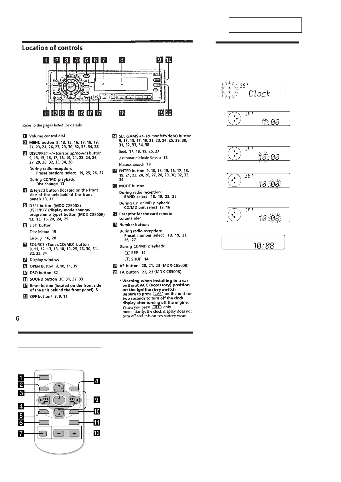
Setting the clock
The clock uses a 12-hour digital indication.
Example: To set the clock to 10:08
1 Press (MENU), then press either side of
(DISC/PRST) repeatedly until “Clock”
appears.
1 Press (ENTER).
The hour indication flashes.
2 Press either side of (DISC/PRST) to set
the hour.
3 Press (+) side of (SEEK/AMS).
Location of controls (MDX-C8500X)
Card remote commander RM-X91
The minute indication flashes.
4 Press either side of (DISC/PRST) to set
the minute.
2 Press (ENTER).
The clock starts.
After the clock setting is completed, the
display returns to normal playback mode.
Tip
You can set the clock automatically with the RDS
feature (see page 24). (MDX-C8500R)
Note
In the initial setting, the clock indication appears
while the unit is turned off.
When you select the “on” setting of the “D.Info”
item (page 29), you can see the clock indication in
the upper part of the display while you are
enjoying any source.
The corresponding buttons of the card
remote commander control the same
functions as those on this unit.
1 OFF button
2 MENU button
3 SOURCE button
4 SEEK/AMS (cursor </,) buttons
5 SOUND button
6 DSPL button
7 ATT button
8 LIST button
9 DISC/PRST (cursor M/m) buttons
0 ENTER button
qa MODE button
qs VOL buttons
DISC
SOURCE
DISC
OPEN/CLOSE
ENTER
VOLATT
OFF
MENU LIST
SEEK SEEK
SOUND
DSPL MODE
4
Page 5
56789
Page 6
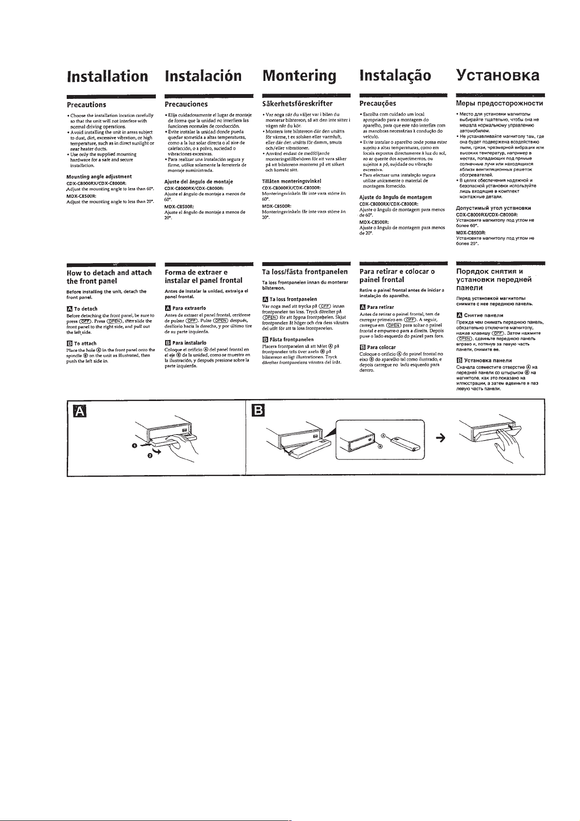
Page 7
Page 8

Page 9
(MDX-C8500R)
Page 10

y
(MDX-C8500X)
Connection example
Exemple de connection
Ejemplo de conexiones
*
from car antenna
de l’antenne de la voiture
de la antena del automóvil
To AMP REMOTE IN of an optional power amplifier.
This connection is only for amplifiers. Connecting any
other system may damage the unit.
Pour effectuer le raccordement à AMP REMOTE IN de
l’amplificateur de puissance en option.
Cette connexion s’applique uniquement aux
amplificateurs. Le branchement de tout autre système
risque d’endommager l’appareil.
Para conectar a AMP REMOTE IN del amplificador de
potencia opcional.
Esta conexión es sólo para amplificadores.
La conexión de cualquier otro sistema puede dañar la
unidad.
Left
Gauche
Izquierdo
Right
Droit
Derecho
Left
Gauche
Izquierdo
Right
Droit
Derecho
to a metal surface of the car
First connect the black ground lead, then connect the
yellow and red power input reads.
vers un point métallique de la voiture
Branchez d‘abord le fil de masse noir et, ensuite, les fils
d‘entrée d‘alimentation jaune et rouge.
a un punto metálico del automóvil
En primer lugar conecte el conductor de puesta a masa
negro y, a continuación, los cables de entrada de
alimentación amarillo
rojo.
BUS AUDIO IN
SUB OUT (MONO)
AMP REM
Max. supply current 0.3 A
Courant max. fourni 0,3 A
Corriente máx. de
alimentación de 0,3 A
*
AUDIO OUT REAR
Blue/white striped
Rayé bleu/blanc
Con raya azul/blanca
White
Blanc
Blanco
White/black striped
Rayé blanc/noir
Con raya blanco/negro
Grey
Gris
Gris
Gray/black striped
Rayé gris/noir
Con raya gris/negro
Green
Vert
Verde
Green/black striped
Rayé vert/noir
Con raya verde/negro
Purple
Mauve
Púrpura
Purple/black striped
Rayé mauve/noir
Con raya púrpura/negro
AUDIO OUT FRONT
8
Black
Noir
Negro
Source selector
(not supplied)
Sélecteur de source
(non fourni)
Selector de fuente
(no suministrado)
Supplied to XA-C30
Fourni avec le XA-C30
Suministrado con el XA-C30
REMOTE IN
BUS
CONTROL IN
Fuse (10 A)
Fusible (10 A)
Fusible (10 A)
Blue
Bleu
Azul
Max. supply current 0.1 A
Courant max. fourni 0,1 A
Corriente máx. de alimentación de 0,1 A
Red
Rouge
Rojo
Light blue
Bleu ciel
Azul celeste
Yellow
Jaune
Amarillo
Insert with the cord upwards.
Insérez avec le câble vers le haut.
Insertar con el cable hacia arriba.
ANT REM
*
RCA pin cord (not supplied)
Cordon à broche RCA (non fourni)
Cable con pines RCA (no suministrado)
Supplied to the CD/MD changer
Fourni avec le changeur de CD/MD
Suministrado con el cambiador de CD/MD
XA-C30
Rotary commander RM-X4S (not supplied)
Satellite de commande RM-X4S (non fourni)
Mando rotativo RM-X4S (no suministrado)
to the power antenna control lead or power supply lead of
antenna booster amplifier
Notes
• It is not necessary to connect this lead if there is no power
antenna or antenna booster, or with a manually-operated
telescopic antenna.
• When your car has a built-in FM/AM antenna in the rear/side
glass, see “Notes on the control and power supply leads.”
vers le fil de commande de l‘antenne électrique ou le fil
d‘alimentation de l‘amplificateur d‘antenne
Remarques
• Il n’est pas nécessaire de raccorder ce fil s’il n’y a pas
d’antenne électrique ni d’amplificateur d’antenne, ou avec
une antenne télescopique manuelle.
• Si votre voiture est équipée d’une antenne FM/AM intégrée
dans la vitre arrière/latérale, voir les “Remarques sur les
câbles de commande et d’alimentation”.
al cable de control de la antena motorizada o al cable de
fuente de alimentación del amplificador de antena
Notas
• Si no se dispone de antena motorizada ni de amplificador de
antena, o se utiliza una antena telescópica accionada
manualmente, no será necesario conectar este cable.
• Si el automóvil incorpora una antena de FM/AM en el cristal
trasero/lateral, consulte “Notas sobre los cables de control y
de fuente de alimentación”.
to the +12 V power terminal which is energized in the
accessory position of the ignition key switch
Notes
• If there is no accessory position, connect to the +12 V power
(battery) terminal which is energized at all times.
Be sure to connect the black ground to it first.
• When your car has a built-in FM/AM antenna in the rear/side
glass, see “Notes on the control and power supply leads.”
à la borne +12 V qui est alimentée quand la clé de contact
est sur la position accessoires
Remarques
• S’il n’y a pas de position accessoires, raccordez la borne
d’alimentation (batterie) +12 V qui est en permanence sous
tension.
Veillez à raccorder le fil noir en premier lieu.
• Si votre voiture est équipée d’une antenne FM/AM intégrée
dans la vitre arrière/latérale, voir les “Remarques sur les
câbles de commande et d’alimentation”.
al terminal de alimentación de +12 V que se active en la
posición auxiliar de la llave de encendido
Notas
• Si no existe posición auxiliar, realice la conexión al terminal
de alimentación (batería) de +12 V que reciba energía
permanentemente.
Asegúrese de conectar primero a este terminal el conductor
de puesta a masa negro.
• Si el automóvil incorpora una antena de recepción de FM/
AM en el cristal trasero/lateral, consulte “Notas sobre los
cables de control y de fuente de alimentación”.
to the interface cable of a car telephone
ATT
vers le cordon de liaison d’un téléphone de voiture
al cable de interfaz de un teléfono para automóvil
to the +12 V power terminal which is energized at all times
Be sure to connect the black ground to it first.
à la borne +12 V qui est alimentée en permanence
Raccordez d‘abord le fil de masse noir.
al terminal de alimentación de +12 V que esté
permanentemente energizado
Asegúrese de conectar primero a este terminal el conductor de
puesta a masa negro.
10
Page 11
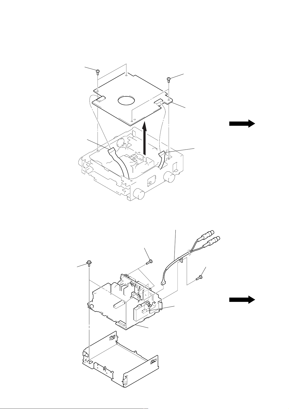
SECTION 3
DISASSEMBLY
Note: Follow the disassembly procedure in the numerical order given.
SUB PANEL ASS’Y
4 two claws
6 sub panel ass’y
3 screw
(PTT2.6 × 8)
1 screw
(PTT2.6 × 6)
2 cover
3 two screws
(PTT2.6 × 8)
MECHANISM DECK (MG-164NV-138)
3 two screws
(PTT2.6 × 10)
5 mechanism deck
(MG-164NV-138)
4 claw
5 connector (CN752)
3 screw
(PTT2.6 × 8)
4 bracket (MD)
1 screw
(PTT2.6 × 6)
2 connector
(CN101)
1 screw
(PTT2.6 × 6)
11
Page 12
SERVO BOARD
d
)
1 sensor flexible board
2 two screws
(BVTT2 × 4)
2 two screws
(BVTT2 × 4)
3 servo board
(CN102)
1 flexible boar
(CN103)
MAIN BOARD
2 three ground point
4 cord (with connector) (sub out)
5 two screws
(PTT2.6 × 10)
3 screw (PTT2.6 × 10
screws
1 connector (CN301)
6 main board
12
Page 13
MD COVER ASS’Y
s
3 MD cover ass’y
cassette holder
1 four screws
(B2 × 3)
shaft (MD cover guide)
HEAT SINK
A
2 Pushing the Cassette Holder in the direction of arrow A with a
screwdriver, etc., disengage the Shaft (MD Cover Guide) from
the slot in the MD Cover Assy.
Note: Take care not to scratch the optiocal Pick-up when pushing
the Cassette Holder with a screwdriver. etc.
1 four screws
(PTT2.6 × 8)
2 two screws
(PTT2.6 × 12)
3 heat sink
1 three screw
(PTT2.6 × 8)
13
Page 14

FLOAT BLOCK
)
3 Pushing arrow A part, raise the float block
up ward at the front to release a lock.
float block
A
lever (lock R)
lever (lock L)
1 tension spring (float B)
1 tension spring (float B
2 two tension springs (float F)
LO MOTOR ASS’Y (LOADING) (M903)
4 Remove the bracket (LO)
in the direction of arrow A.
1 Remove solders of motor (M903)
A
5 LO motor ass’y (loading)
(M903)
2 tension spring (rack)
3 claw
14
bracket (LO)
– bottom view –
Page 15

LEVER (LE) ASS’Y
2 stopper washer
2 lever (LE) ass’y
3 roller (gear E)
1
HOLDER ASS’Y
2 type-E stopring 1.5
1 spring (chucking)
2 type-E stopring 1.5
3 lever (lock R)
4 Remove the holder ass’y in the
direction of the arrow.
2 type-E stopring 1.5
3 lever (lock L)
2 type-E stopring 1.5
1 spring (chucking)
15
Page 16
CHUCKING ARM ASS’Y
y
holder ass’y
1 Remove the chucking arm ass’y
in the direction of the arrow.
OPTICAL PICK-UP (KMS-241C/J1NP)
7 optical pick-up
(KMS-241C/J1NP)
1 two screws
(K2 × 3)
2 guide shaft (OPT L)
4 screw
(B2 × 3)
6 bearing (SL)
5 feed screw ass’
3 screw
(K2 × 3)
16
Page 17
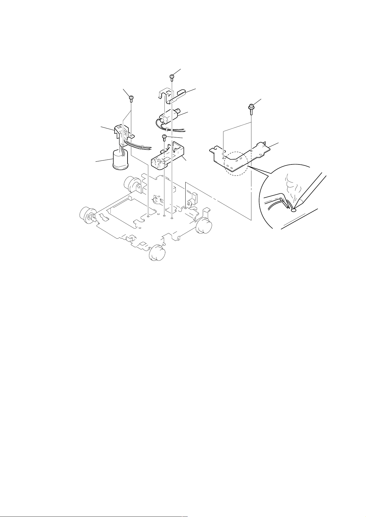
SL MOTOR ASS’Y (SLED) (M902), SP MOTOR ASS’Y (SPINDLE) (M901)
4 screw
(P1.7 × 1.8)
5 bracket (SL)
9 two screws
(P1.7 × 1.8)
0 bracket (SP)
qa SP motor ass’y
(spindle) (M901)
7 screw
(B2 × 3)
2 two screws
(2 × 8)
3 sensor board
1 Remove solders of motors
(M901, M902)
8 base (SL)
6 SL motor ass’y
(sled) (M902)
17
Page 18

SECTION 4
ELECTRICAL ADJUSTMENTS
TEST MODE
This set have the test mode function.
<Set the Test Mode>
1. Turn ON the regulated power supply. (The clock is displayed)
Note: Press the [OFF] button, if the clock is not displayed.
2. Push the preset [4] button.
3. Push the preset [5] button.
4. Press the preset [1] button for more than two seconds.
5. Then the display indicates all lights, the test mode is set.
<Release the Test mode>
1. Push the [OFF] button.
MD SECTION
MD section adjustments are done automatically in this set.
TUNER SECTION
Tuner section adjustments are done automatically in this set.
18
Page 19

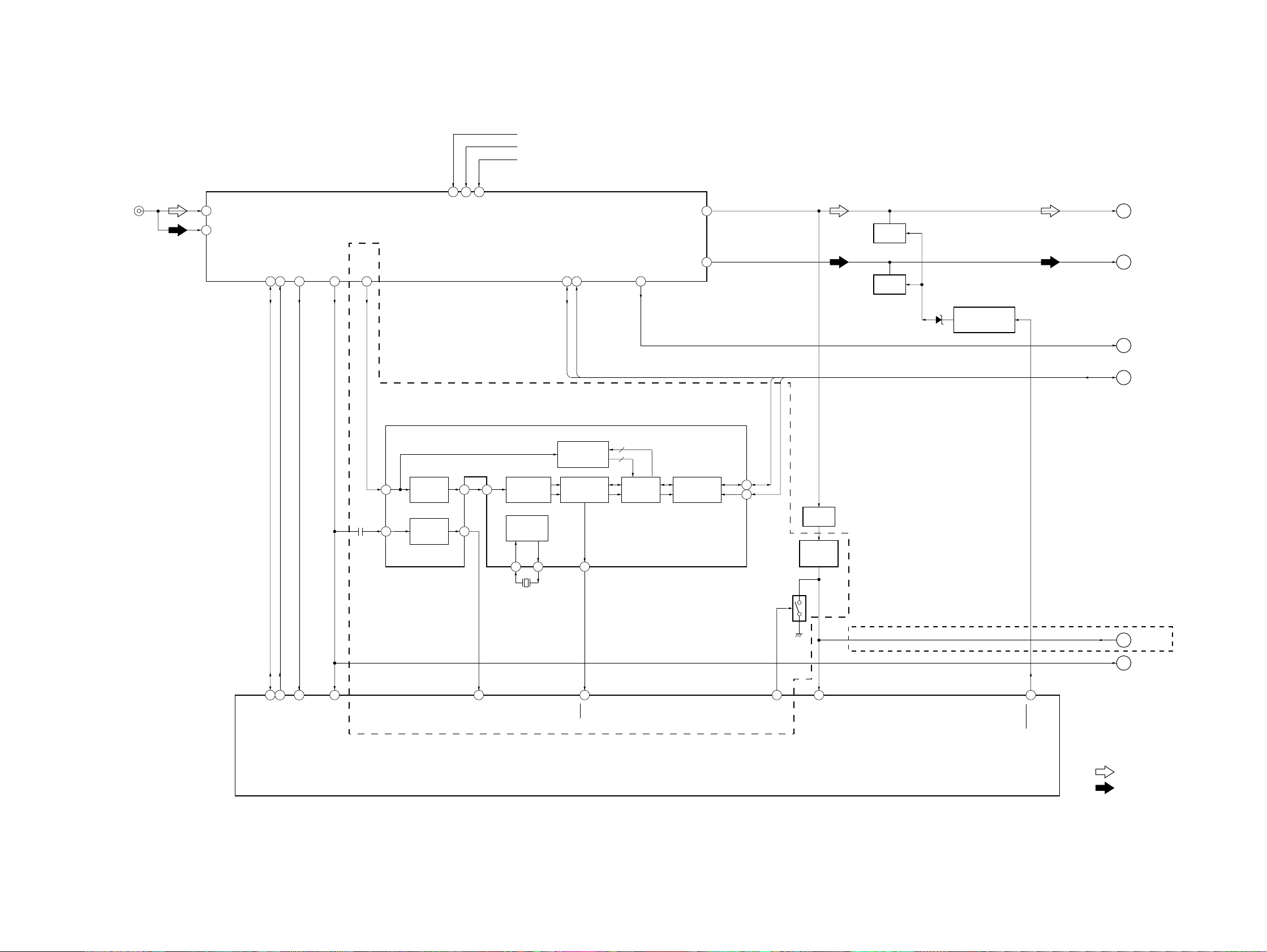
5-1. BLOCK DIAGRAM – SERVO Section –
SECTION 5
DIAGRAMS
100
EFMO
MDX-C8500R/C8500X
15
TX
IC301 (1/2)
ADDT
• SIGNAL PATH
23
: MD PLAY
05
F
C B
I J
D A
E
DETECTOR
LASER DIODE
LDPD
OPTICAL PICK-UP BLOCK
(KMS-241C)
2-AXIS
DEVICE
(FOCUS)
(TRACKING)
ILCC
PD
M901
(SPINDLE)
M902
(SLED)
FCS+
FCS–
TRK+
TRK–
FILI
59
PCO
58
61
FILTER
60
RF AMP,
FOCUS/TRACKING ERROR AMP
48 47
MORFI
MORFO
IC303
I
1
RF AMP
J
2
A
4
B
5
I-V
C
AMP
6
D
7
E
8
I-V
F
AMP
9
APC
PD
IN4R
IN4F
IN2F
IN2R
IN1F
IN1R
IN3F
IN3R
LD/PD
16PSB
3
4
29
30
19
18
14
15
11
10
AMP
SPFD
SPRD
RFO
B.P.F.
AT
AMP
12
46
3T
APCREF
IC306
WBL
B.P.F.
ABCD
AMP
WBL3TEQ
V-I
CONVERTER
F0CNT
20
APCREF
83
SFDR
92
SRDR
91
FFDR
88
FRDR
89
TFDR
86
TRDR
85
TEMP
ADFM
29 30
FOCUS
ERROR AMP
TRACKING
ERROR AMP
+3.3V
PWM GENERATOR
40
I
J
B
A
C
D
E
F
AUTOMATIC
POWER
CONTROL
Q302
FOCUS/TRACKING COIL DRIVE,
SPINDLE/SLED MOTOR DRIVE
6
27
25
21
23
12
10
8
OUT4F
OUT4R
OUT2F
OUT2R
OUT1F
OUT1R
OUT3F
OUT3R
M
M
IC302
AGCI
RF AGC
& EQ
EQ
PEAK &
BOTTOM
ADIN
COMMAND
SERIAL/
PARALLEL
CONVERTER,
DECODER
SCLK
SWDT
1716 18
PEAK HOLD
Q301
+3.3V
13
RECP
AUTOMATIC
POWER
CONTROL
DIGITAL
SERVO
SIGNAL
PROCESS
DIGITAL SERVO
SIGNAL PROCESSOR
IC301 (2/2)
WBL
XLAT
RF
AUX
PEAK
BOTM
ADFG
ABCD
FE
TE
SE
ABCD
AUX1
38
33
37
36
32
35
34
26
28
7465647566 63
FE
TE
AUX2
ABCD
ANALOG MUX
A/D CONVERTER
FROM CPU
INTERFACE
AUTO
SEQUENCER
73 62
SE
PEAK
XLRF
CKRF
DTRF
51
52
55
78
79
BOTM
CLTV
FILO
ASYO
ASYI
COMPA-
RFI
RATOR
ADIP
ADFG
DEMODULATOR/
DECODER
F0CNT
X501
10MHz
80
81
82
PLL
EFM/ACIRC
ENCODER/DECODER
SUBCODE
PROCESSOR
SPINDLE
SERVO
SPFD
SPRD
DQSY11SQSY14XINT
XRST
94 93
10
12
59 62 55 54 52 45 51 64 26 27 28 29
MD-RST
31
EXTAL
XTAL
32
7 6
LOADING
MOTOR DRIVE
IC305
M903
(LOADING)
5 4
RIN FIN
OUT1 OUT2
1 7
SHOCK PROOF
MEMORY CONTROLLER
51331
LEVEL SHIFT
IC502
61242
SQSY
CC-XINT
EJECT
LOAD
M
ATRAC
CPU
INTERFACE
SENS
SRDT
SWDT
9 8 5 6 7
SWDT
SENS
MD-SI
MD-SO
MD MECHANISM CONTROLLER
ON: When the disc loading start
and the disc eject completion.
SAMPLING
RATE
CONVERTER
DIGITAL
AUDIO
ENCODER/DECODER
INTERFACE
D-RAM
INTERNAL BUS
MONITOR
CONTROL
SCLK
XLAT
MNT0
1 2 3 4
13
LEVEL SHIFT
IC503
12
FOK
SCLK
XLAT
MNT0
MD-LAT
MD-CKO
IC501 (1/2)
C-SW
63
LOADING START/
EJECT END
DIN
DOUT
DADT
MNT1
MNT2
MNT3
135
246
SHOCK
XBUSY
SLOCK
MNT1
MNT2
MNT3
ON: When completion of
DIGITAL SIGNAL PROCESSOR,
EFM/ACIRC ENCODER/DECODER,
SHOCK PROOF MEMORY CONTROLLER,
ATRAC ENCODER/DECODER, 2M BIT D-RAM
21
22
24
LOADING
END
the disc loading.
IC301 (1/2)
BCK
LRCK
2526 27
LRCK
XBCK
FS256
CLOCK
GENERATOR
TH501
39
TEMP
E-SW
11 56
OSCI
OSCO
XOE
XWE
XRAS
XCAS
EMPHASIS
66
DEEMP
(LIMIT)
ON: When the optical pick-up is
inner position.
A-MUTE
16
17
D0 – D3A00 – A09
47, 46, 48, 49
32 – 29, 34 – 38, 43
41 22
45 3
44 4
42 23
67
LIMIT-IN
DADT, BCK, LRCK, 512FS
512FS
512FS OSC
IC304
D0 – D3
1, 2, 24, 25
A0 – A9
9 – 12, 14 – 18, 5
OE
WE
RAS
CAS
D-RAM
IC307
EMPHASIS
MD-ATT
(Page 21)
A
(Page 21)
B
C
(Page 21)
1919
Page 20
MDX-C8500R/C8500X
5-2. BLOCK DIAGRAM – TUNER Section –
CN102
(FM/AM ANTENNA)
FM/AM TUNER UNIT
TUX201
FM-ANT
2
AM-ANT
1
EEPROM SDA
EEPROM SCL
17
18
FMAGC
4
SMETER
14
RDSDET
9
11
5
B/U 5V
VCC
16
TUNER 5V
B/U +5V
TUNER VCC
TUNER +5V
SDA
12 13
SCL
19
AM IF
MPX
AMDET
10
MUTING
Q202
8
MUTING
Q205
MUTING
CONTROL SWITCH
D202
Q206, 207
MPX
AM
AM IF
D
E
F
(Page 21)
(Page 21)
(Page 21)
DATA
(MDX-C8500R)
RDS DECODER
IC201
PATH
OUT
SC
MPTH
CIN
19
CLOCKED
COMPARATOR
OSCILLATOR
& CLOCK
OSCI
OSCO
4
5
X101
4.332MHz
18
2
52
MPX
LVIN
57 kHz
BAND-PASS
FILTER
MULTI
DETECTOR
16
20
10
11
51
53
CLOCK
SIGNAL
QUALITY
DECODER
RDS/RDBS
DEMODULATOR
& DECODER
DAVN
8
75
5
4
INTERFACE
REGISTER
IIC BUS
SLAVE
TRANSCEIVER
SDA
SCL
9
10
NOISE DET
DISCHARGE
DATA
Q208
SWITCH
56
CLOCK
BUFFER
Q209
BAND-PASS
FILTER
IC202
50
32
DATA, CLOCK
QUALITY
SMETER
(Page 21)
H
(MDX-C8500X)
(Page 21)
I
(Page 21)
G
T.ROM-SCL
T.ROM-SDA
FMAGC
VSM
MTP
DAVN
MASTER CONTROLLER
IC502 (1/4)
NS-MASK
QUALITY
TUMUTE
• SIGNAL PATH
: FM
05
: AM (MW/LW)
2020
Page 21
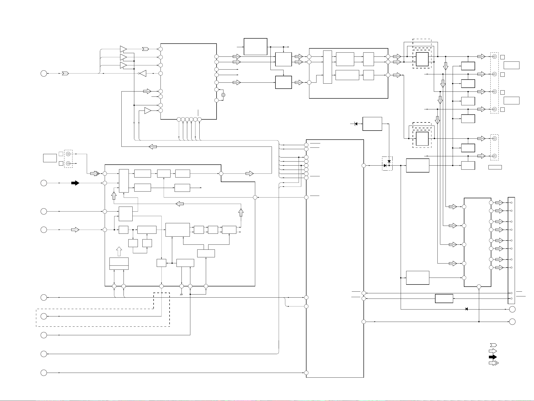
5-3. BLOCK DIAGRAM – MAIN Section –
MDX-C8500R/C8500X
(Page 19)
(Page 20)
(Page 20)
(Page 20)
(Page 20)
(Page 20)
(Page 20)
(Page 22)
(Page 19)
05
DADT,
BCK,
LRCK,
512FS
A
CN302 (1/2)
BUS
AUDIO IN
AM
E
AM IF
F
MPX
D
DATA, CLOCK
H
QUALITY
I
SMETER
G
DSPDATA, DSPCKO
J
EMPHASIS
B
LEVEL SHIFT
IC803 (1/2)
DADT
9
8
LRCK
BCK
512FS
L
R
R-CH
INPUT SELECT, FM MPX
SEL
1
AM
11
AMIF
12
MPX
13
CONTROL
SDA
20
DATA
10
2
3
1
5
6
4
IC806
12
LEVEL SHIFT
IC803 (2/2)
XMST
DSPPLL
IC301 (1/2)
LOUDNESS/
VOLUME
INPUT
MULTIPLEXER
AM/FM
NOISE
BLANKER
L.P.F.
DIGITAL
IIC BUS
SCL
21 18
CLOCK
CANCELATION
PLL
R-CH
PILOT
PILOT
DET
11
(MDX-C8500X)
DIGITAL SIGNAL PROCESSOR,
SI1
71
76
LRCK
75
BCK
81
PLCLK
35
LIN
46
RIN
77
XMST
82
XECKSTP
SOFT
MUTE
LOUDNESSMUTE
DEMODULATOR
+STEREO ADJUST
+STEREO BLEND
QUAL
QUALITY
DIGITAL FILTER,
D/A CONVERTER
IC805
TRDT
RVDT59SCK
63
62 57
TRDT
XLAT
SCK
RVDT
TONE
CONTROL
MULTIPATH
DETECTOR
MPOUT16MPIN
15
ANALOG +8V
FL-OUT
27
AOUTL1
AOUTR1
AOUTR3
AOUTL3
AOUTR2
XTLI38
XTLO38
XLAT
REDY
XRST
6061
REDY
DSPRST
TO
OUTPUT
SELECTOR
L.P.F. S & H HIGH-CUT
D/A
CONVERTER
LEVEL
14
ACOUTL
29
54
52
43
41
40
RL-OUT
FR-OUT
RR-OUT
SUB-OUT
38
X801
16.9344MHz
CENTER VOLTAGE
GENERATOR
(FOR BIAS)
IC809 (2/2)
R-CH
R-CH
SM
R-CH
ELECTRICAL VOLUME
R-CH
LOW-PASS
FILTER
IC807
LOW-PASS
FILTER
IC809 (1/2)
XMST
DSPPLL
TRDT
RVDT
SCK
XLAT
REDY
DSPRST
DSPDATA
DSPCKO
18
DATA
CLOCK
34
33
35
29
28
25
26
27
35
78
36
31
70
71
ACINLF
ACINLR
SWINR
DSPMST
DSPPLL
DSPSI
DSPSO
DSPCKO
DSPLAT
DSPREADY
DSPRST
VOLATT
I2C SDA
I2C SCL
IC301 (2/2)
MONO FADER MIXER
OUTPUT
SELECTOR
SUBWOOFER
+PHASE CONTROL
BATT B+
MASTER CONTROLLER
IC502 (2/4)
D352
ATT
TESTIN
TELATT
AMPON
MONO
FADER
BATTERY OFF
MUTE DRIVER
Q352
5
84
96
55
OUTLF
OUTLR
OUTSWR
30
29
25
D354
(MDX-C8500R)
LINE
DRIVER
IC303
(MDX-C8500X)
R-CH
R-CH
(MDX-C8500R)
LINE
DRIVER
IC304
(MDX-C8500X)
R-CH
MUTING
CONTROL SWTICH
Q354, 355
MUTING
CONTROL SWITCH
Q353
LEVEL SHIFT
Q111
MUTING
Q356
MUTING
Q357
MUTING
Q358
MUTING
Q359
MUTING
Q360
MUTING
Q361
IN2
12
14
IN4
11
IN1
IN3
15
MUTE
22
D353
POWER AMP
IC351
OUT2+
OUT2–
OUT4+
OUT4–
OUT1+
OUT1–
OUT3+
OUT3–
STBY
4
CN302 (2/2)
CN301
SUB OUT
5
3
21
23
9
7
17
19
MD-ATT
AMPON
L
AUDIO
OUT FRONT
R
L
AUDIO
OUT REAR
R
(L)
(R)
CN101 (1/2)
(POWER CONNECTOR)
1
FL+
9
FL–
4
FR+
12
FR–
2
RL+
10
RL–
3
RR+
11
RR–
15
TEST
13
TEL-ATT
C
(Page 19)
K
(Page 23)
• SIGNAL PATH
: MD PLAY
: FM
: AM (MW/LW)
: BUS AUDIO IN
97
EMPH
2121
Page 22

MDX-C8500R/C8500X
5-4. BLOCK DIAGRAM – DISPLAY/KEY CONTROL Section –
(Page 21)
REMOTE IN
DSPDATA,DSPCKO
J
J651
D611
48 72
TRDT
61
RCIN0
SCK
63
SP-SI
RCIN1
SA LAT
4
33 57
SP-LAT
SP-SCK
LSW751,901–917,
S901 – 904
46
47
KEYIN1
KEYIN0
BOOT
106
X105
18.432MHz
85
86
BOOT
EXTAL
LIQUID CRYSTAL DISPLAY
DRIVE CONTROLLER
IC701 (1/2)
XTAL
D701
ROTARY
ENCODER
RE901
116 115
REIN0
RX
12
MAIN BODY SIDE
62
RX
CN701
RE901
VOLUME/BASS/
TREBLE/BALANCE/
FADER CONTROL
REIN1
CN901
FRONT PANEL SIDE
14 1
79
KEYACK
TX
13
KEY ACTIVE
SWITCH
Q701, 702
80
AD-ON
MASTER CONTROLLER
IC502 (3/4)
MDX-C8500R : LSW901 – 908,
MDX-C8500X : LSW901 – 908,
B/U +5V
LSW910 – 917
LSW912 – 917
(NOSE DETECT)
117
NOSE-SW
S102
BUZZER
DRIVE
Q351
15
BEEP
LCD B+
BZ101
(BUZZER)
(LCD BACK LIGHT)
LED751
(MD DISC SLOT),
LSW751
LED910 – 915
B+ SWITCH
Z
X1
93
X104
3.68MHz
Q751, 752
118
DOORIND
X1A
73
X103
32.768kHz
X0A
74
X0
92
LCD B+
TX/LCD-DATA
LCD-SCK
LCD-CE1
60
64 66
C953, R957
OSC
100
99
98
LCD-CE
LCD-CLK
LCD-DATA
SEG1 – SEG74
1 – 74
LIQUID CRYSTAL DISPLAY
05
LCD901
COM1 – COM8
83 – 76
96
OSC
LED
DRIVE
Q902
85
(MDX-C8500R) (MDX-C8500R)
(MDX-C8500X)
GREEN
LIQUID CRYSTAL DISPLAY DRIVER
IC901
LED
DRIVE
Q901
84
AMBER
(MDX-C8500X)
LED DRIVE
Q903
86
DIMMER
2222
Page 23
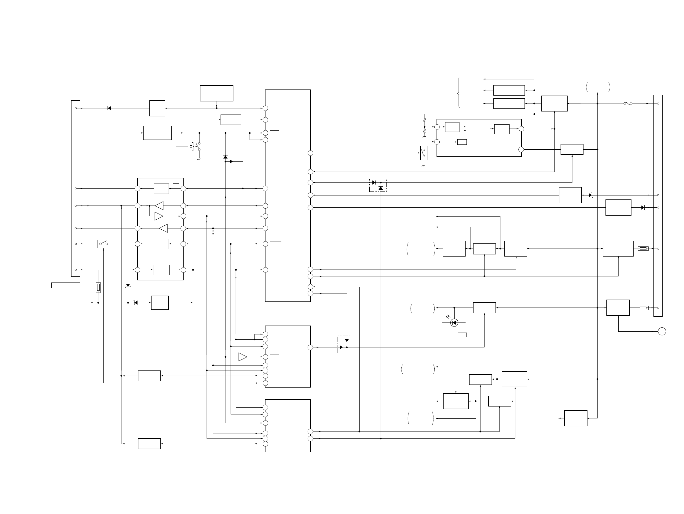
5-5. BLOCK DIAGRAM – BUS CONTROL/POWER SUPPLY Section –
MDX-C8500R/C8500X
SIRCS
RESET
DATA
CLK
BUS ON
3
2
5
4
6
D605
BUS ON SWITCH
Q603
B/U +5V
SIRCS
BUFFER
Q605
RESET SIGNAL
GENERATOR
IC503
SONY BUS INTERFACE
IC601
RST
DATA
CLK
BUS ON
OUT
RESET
SWITCH
BUS ON
SWITCH
2
6
4
1
RST
DATA IN
DATA OUT
CLK IN
BUS
ON IN
S101
RESET
13
11
12
MASTER CONTROLLER
24
85
90
86
18
17
6
9
4
SIRCS
RAMBU
RESET
HSTX
SYSRST
UNISO
UNISI
UNICKO
BUS-ON
IC502 (4/4)
F CH
FSW IN
DSPON
ACCIN
ILLIN
DSP CIRCUIT B+
IN
ERROR
4
AMP
RT
OSC SWITCH
98
65
110
D104
81
95
Q101
ANALOG +8V
TUNER VCC
(TUNER CIRCUIT B+)
TUNER +5V
TUNER CIRCUIT/
RDS DECODER
(IC201) B+
7
+5V
REGULATOR
Q201
REMOTE CONTROL
RECEIVER
IC951
D502
RAM RESET
IC504
D614
B/U +5V
9
8
DSP +5V
DIGITAL +3.3V
ANALOG +3.3V
PWN
COMPARATOR
OSC
+3.3V REGULATOR
+3.3V REGULATOR
OUTPUT
CIRCUIT
POWER CONTROL
IC302
B+ SWITCH
Q203, 204
IC802
IC801, Q801
OUT
VCC
+8V
REGULATOR
Q107 – 109
SWITCHING
REGULATOR
Q103, 105 106
1
2
B+ SWITCH
Q102, 104
ACCESSORY
CHECK
Q112
BATT B+
POWER AMP
(IC351) B+
D109
F1
ILLUMINATION
LINE DETECT
Q113
ANTENNA REMOTE
SWITCH
Q364, 366
CN101 (2/2)
(POWER CONNECTOR)
16
7
D108
14
TH103
6
+B
ACC
ILL
ANT-R
BATT
CN601
BUS CONTROL IN
(FOR SONY BUS)
7
BATT B+
TH101
3
D607
D603
BATT
BATTERY
LEVEL SHIFT
Q602
LEVEL SHIFT
Q601
BATTERY
SWITCH
DETECT
Q604
BU IN
PWON
TUNON
CDMD ON
FLASH ON
MDMON
83
113
116
82
52ILL-ON
65MD-ON
10
D703
LCD B+
LCD DRIVER
(IC901) B+
LO +12V
LOADING MOTOR
DRIVER (IC306) B+
+3.3V
DRIVER +5V
MOTOR/COIL
DRIVER
(IC303) B+
LED901 – 904 (ILLUMINATION)
LSW909 DSO
B+ SWITCH
Q402, 403
VCC
+3.3V
REGULATOR
IC401, Q401
REGULATOR
Q703 – 705
B+ SWITCH
Q406, 407
+12V
REGULATOR
Q401, 404, 405
B/U +5V
+5V
REGULATOR
Q110
AMP REMOTE
SWITCH
Q363, 365
TH102
AMPON
5
K
(Page 21)
AMP-R
BU-IN
10
LEVEL SHIFT
77
LIQUID CRYSTAL DISPLAY
82
NMI (H)
49
BU-IN
BUS-ON
38
IC702
81
RESET
101
UNICKI
UNISI
98
UNISO
97
LINK OFF
50
MD MECHANISM CONTROLLER
60
BU-IN
BUS-ON
61
30
RESET
48
UNICKIO
49
UNISI
UNISO
50
DRIVE CONTROLLER
IC701 (2/2)
IC501 (2/2)
05
2323
Page 24
5-6. NOTES FOR PRINTED WIRING BOARDS AND SCHEMATIC DIAGRAMS
• Circuit Boards Location
Note on Printed Wiring Board:
• X : parts extracted from the component side.
• Y : parts extracted from the conductor side.
z
•
•
: Through hole.
f
: internal component.
• b : Pattern from the side which enables seeing.
(The other layers' patterns are not indicated.)
Caution:
Pattern face side: Parts on the pattern face side seen from
(Conductor Side) the pattern face are indicated.
Parts face side: Parts on the par ts face side seen from
(Component Side) the parts face are indicated.
Note on Schematic Diagram:
• All capacitors are in µF unless otherwise noted. pF: µµF
50 WV or less are not indicated except for electrolytics
and tantalums.
• All resistors are in Ω and 1/
specified.
f
•
: internal component.
4
W or less unless otherwise
• C : panel designation.
Note: The components identified by mark 0 or dotted line
with mark 0 are critical for safety.
Replace only with part number specified.
• U : B+ Line.
• Power voltage is dc 14.4V and f ed with regulated dc power
supply from ACC and BATT cords.
• Voltages are taken with a V OM (Input impedance 10 MΩ).
Voltage variations may be noted due to normal production tolerances.
• Waveforms are taken with a oscilloscope.
Voltage variations may be noted due to normal production tolerances.
• Circled numbers refer to waveforms.
• Signal path.
F : FM
f : AM (MW/LW)
L : BUS AUDIO IN
E : MD PLAY
• Please refer to servicing notes (page 3) for system of
TYPE A, B and C.
SENSOR board
DSO board
SERVO board
SUB board
KEY board
MAIN board
2424
Page 25
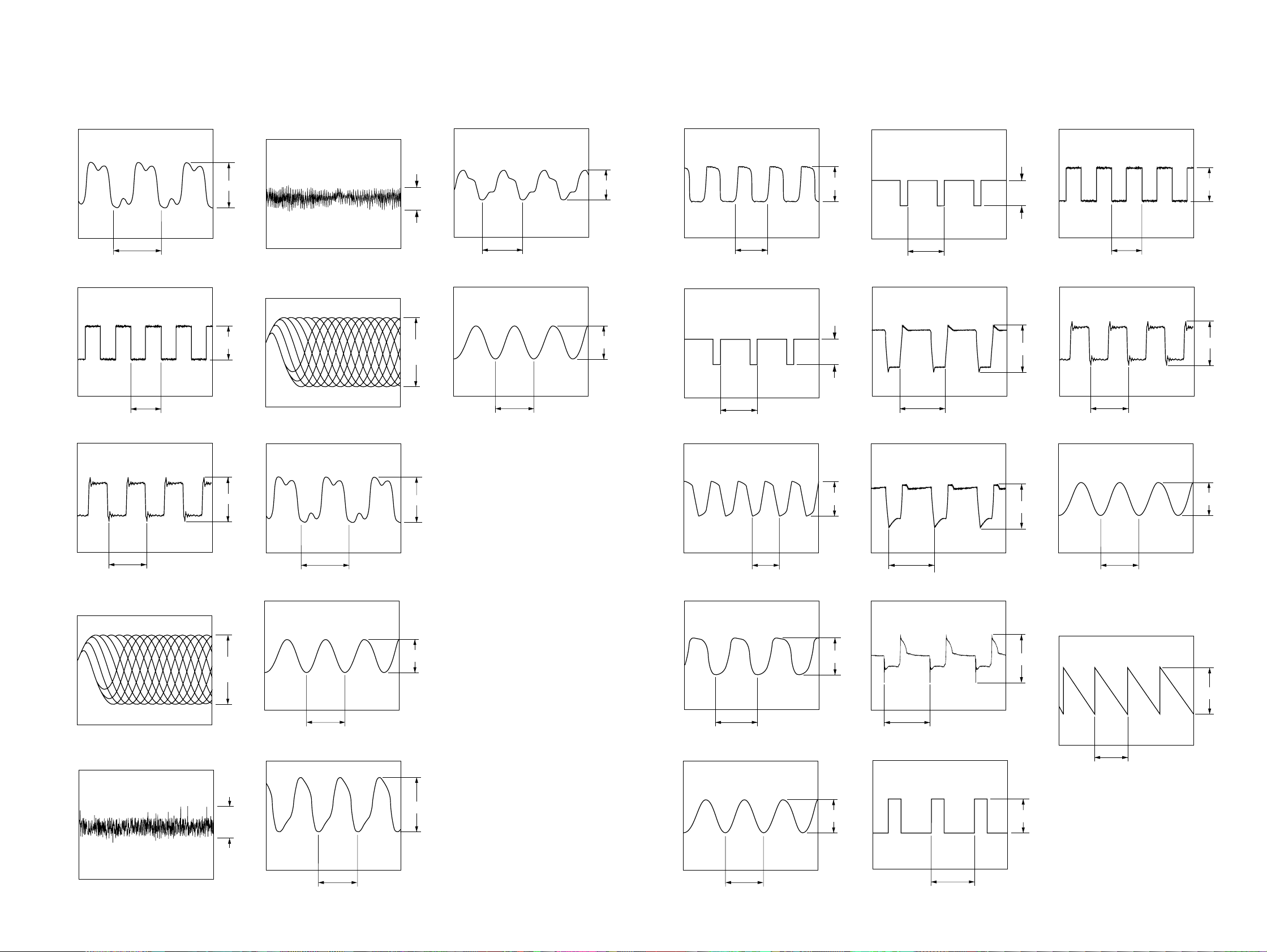
• Waveforms
– SERVO Board –
– MAIN Board –
– DSO Board –
1 IC301 qh (OSCI) (MD Play Mode)
4.6 Vp-p
44.3 ns
2 IC301 wg (LRCK) (MD Play Mode)
3.8 Vp-p
22.7 µs
3 IC301 wh (XBCK) (MD Play Mode)
6 IC301 uf (TE), IC302 wh (TE)
(MD Play Mode)
Approx.
2 Vp-p
7 IC302 1, 2, r;, rh (I, J, AGCI, RFO)
(MD Play Mode)
Apporx.
0.6 Vp-p
8 IC304 1, 2 (MD Play Mode)
qa IC304 7 (MD Play Mode)
44.3 ns
qs IC501 ea (EXTAL)
101 ns
4.4 Vp-p
3.7 Vp-p
1 IC201 4 (OSCO)
231 ns
2 IC502 yg (F OSC)
3.4 µs
3 IC502 ud (X1A)
5.8 Vp-p
4.6 Vp-p
6 IC302 1 (OUT)
3.4 µs
7 Q103, 106 (Base)
3.4 µs
8 Q103, 106 (Emitter)
12.6Vp-p
7 Vp-p
1 IC803 3 (MD Play Mode)
3.9 Vp-p
22.7 µs
2 IC803 6 (MD Play Mode)
4 Vp-p
354 ns
3 IC805 ra (XTLI38)
354 ns
4 IC301 tg (RFI), IC302 ek (RF)
(MD Play Mode)
5 IC301 yg (FE), IC302 ef (FE)
(MD Play Mode)
4.1 Vp-p
Apporx.
1.5 Vp-p
Approx.
0.5 Vp-p
44.3 ns
9 IC304 3 (MD Play Mode)
44.3 ns
0 IC304 5, 6 (MD Play Mode)
4.1 Vp-p
2.6 Vp-p
3.8 Vp-p
30.5 µs
4 IC502 od (X1)
272 ns
5 IC701 ih (EXTAL)
6 Vp-p
6.1 Vp-p
3 Vp-p
3.4 µs
9 Q105 (Base)
3.4 µs
0 Q105 (Collector)
6.6 Vp-p
3.6 Vp-p
15.2 Vp-p
2.7 Vp-p
59.1 ns
– KEY Board –
1 IC901 oh (OSC)
3.1 Vp-p
22.7 µs
44.3 ns
54.2 ns
3.4 µs
2525
Page 26
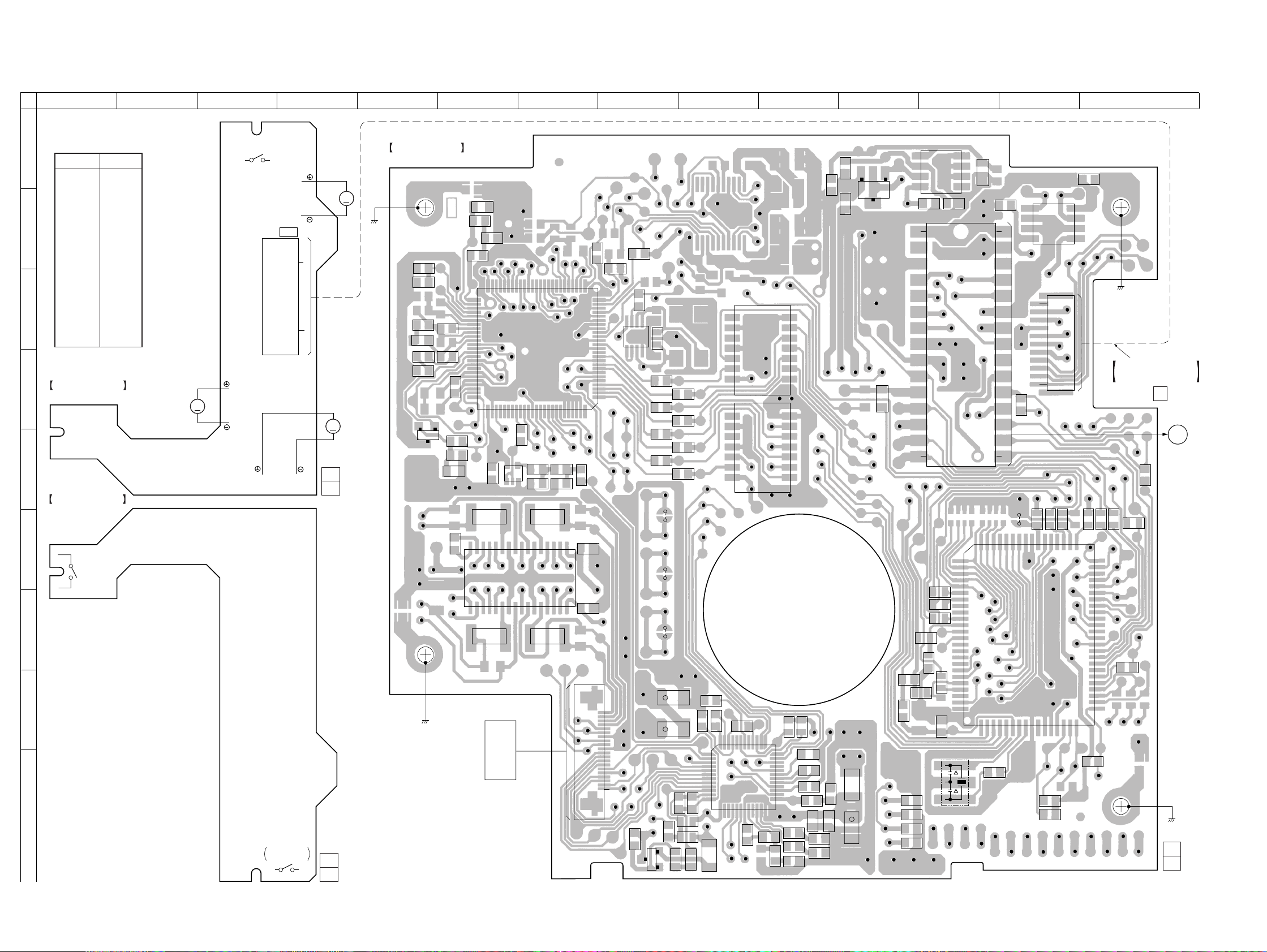
MDX-C8500R/C8500X
5-7. PRINTED WIRING BOARDS – SERVO Board (Component Side)/SENSOR Board –• See page 24 for Circuit Boards Location.
• Semiconductor
A
B
C
D
Location
Ref. No. Location
D401 A-12
D501 D-11
IC301 D-7
IC302 I-9
IC303 F-7
IC304 C-8
IC305 B-13
IC306 E-6
IC401 A-12
IC501 G-13
IC502 D-10
IC503 E-10
Q301 E-5
Q302 I-8
Q401 B-11
SENSOR BOARD
(COMPONENT SIDE)
E
SENSOR BOARD
(CONDUCTOR SIDE)
F
G
1
(LIMIT)
2 3 4 5 6 7 8 9 10 11 12 13 14
M902
(SLED)
(LOADING END)
M903
(LOADING)
RED
MM
BLK
11
1
RED
MM
BLK
RED
1-676-656-
BLK
MM
11
(11)
M902
(SPINDLE)
SERVO BOARD
(COMPONENT SIDE)
(CHASSIS)
R320
C308
R325
C310
R328
C311
Q301
R324
R327
C306
R319
C305
R318
50 26
51
IC301
R314
25
R313
8
IC304
1
R311
FB302
5
4
R354
5
B
E
R404
8
7
C402 R405
C
Q401
8
C403 C406
29 30
IC502
IC401
CN101
4
K
A
1
D401
C352
1
C11
8
IC305
4
11
CN103
5
(CHASSIS)
SENSOR FLEXIBLE
C314C339
75
76
BCE
R329
R330
C315
L304
32 17
C348
5
IC306
1
R331
4
R353
R352
C343
3
C342
L303
1
100
R351
C349
R308
R307
R306
R305
R304
R303
R302
R301
14
8
IC503
14
IC303
116
L305
L306
C336
1
7
1
D501
R538
IC501
1
1-654-693-
R525
R524
R523
R522
65
R518
R537
R536
64
K
A
12
80
1
R501
R502
R503
R531
BOARD
11
(Page 31)
R517
A
MAIN BOARD
CN301
C516
R535
+
C318
R355
CN102
1
C331
R356
+
C319
20
C320
R337
C321
R348
C322
Q302
BCE
R349
R357
C329
1
IC302
12
R341
R350
C328
36
25
R339
R345
R343
R338
C330
C327
C326
C325
R347
C324
R344
R342
R346
C347
L302
+
C346
3748
2413
R340R336
R505
R527
R528
R526
R529
H
(CHASSIS)
OPTICAL
PICK-UP
BLOCK
(KMS-241C)
I
LOADING START
EJECT END
05
1-676-656-
11
(11)
R539
R504
C501
X501
24
25
R532
40
R507
R506
R511
41
R516
1-675-655-
(CHASSIS)
11
(11)
2626
Page 27

5-8. PRINTED WIRING BOARD – SERVO Board (Conductor Side) –• See page 24 for Circuit Boards Location.
MDX-C8500R/C8500X
1
2 3 4 5 6 7 89
• Semiconductor
A
B
C
D
SERVO BOARD
(CONDUCTOR SIDE)
R547
L501
C510
Q402
R358
BCE
Q403
R402
R403
C511
L301
C344
+
C345
C359
C353
C302
C362
+
C361
15913
IC307
C307
26221814
C309
C358
C301
C317
C356
C357
R401
B
E
C
Location
Ref. No. Location
IC307 C-8
Q402 B-4
Q403 B-4
+
C504
C506
C505
R542
C512
R540
E
R534
R533
C515
F
C514
C513
R521R520
R332
G
R519
H
R512
C503
R510
TH501
RB503
R334
R333
R335
RB301RB302
C333
C316
+
C351
C350
I
05
1-675-655-
11
(11)
2727
Page 28
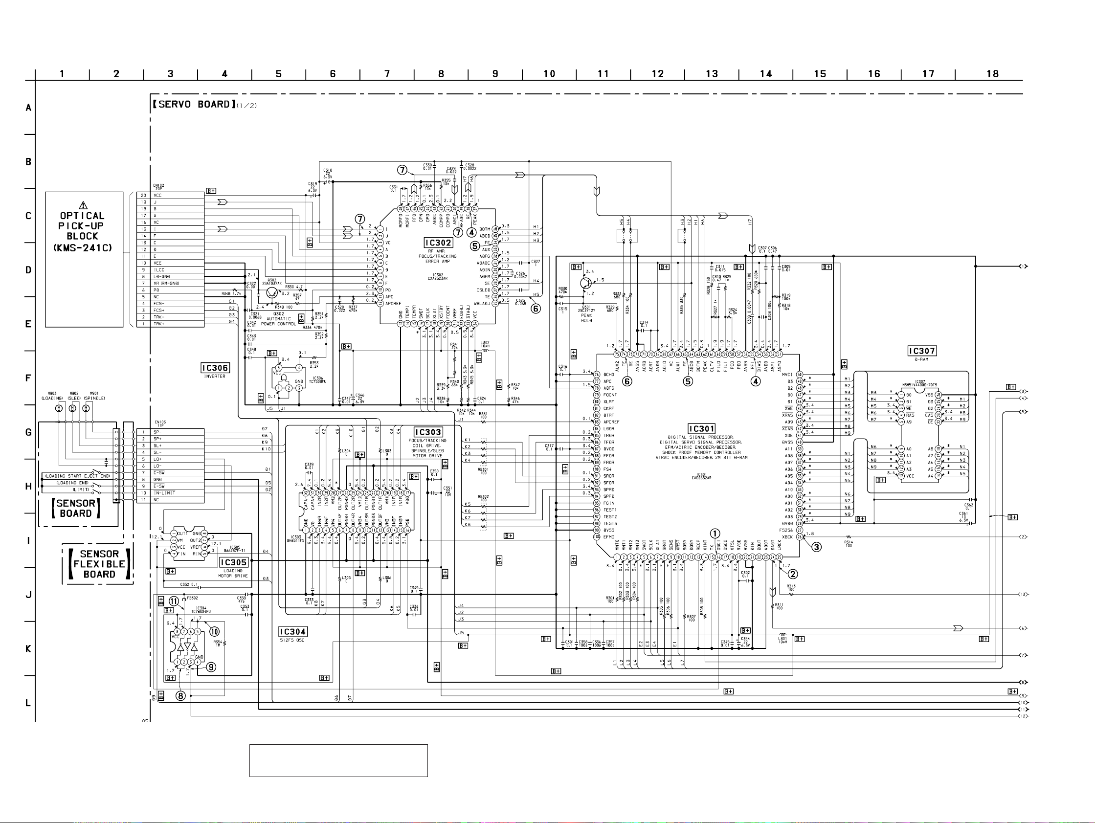
MDX-C8500R/C8500X
5-9. SCHEMATIC DIAGRAM – SERVO Board (1/2)/SENSOR Board –• See page 25 for Waveforms. • See page 42 for IC Block Diagrams.
• Voltages and waveforms are dc with respect to ground
under no-signal conditions.
no mark : MD PLAY
: Impossible to measure
∗
The components identified by mark 0 or dotted
line with mark 0 are critical for safety.
Replace only with part number specified.
2828
Page 29
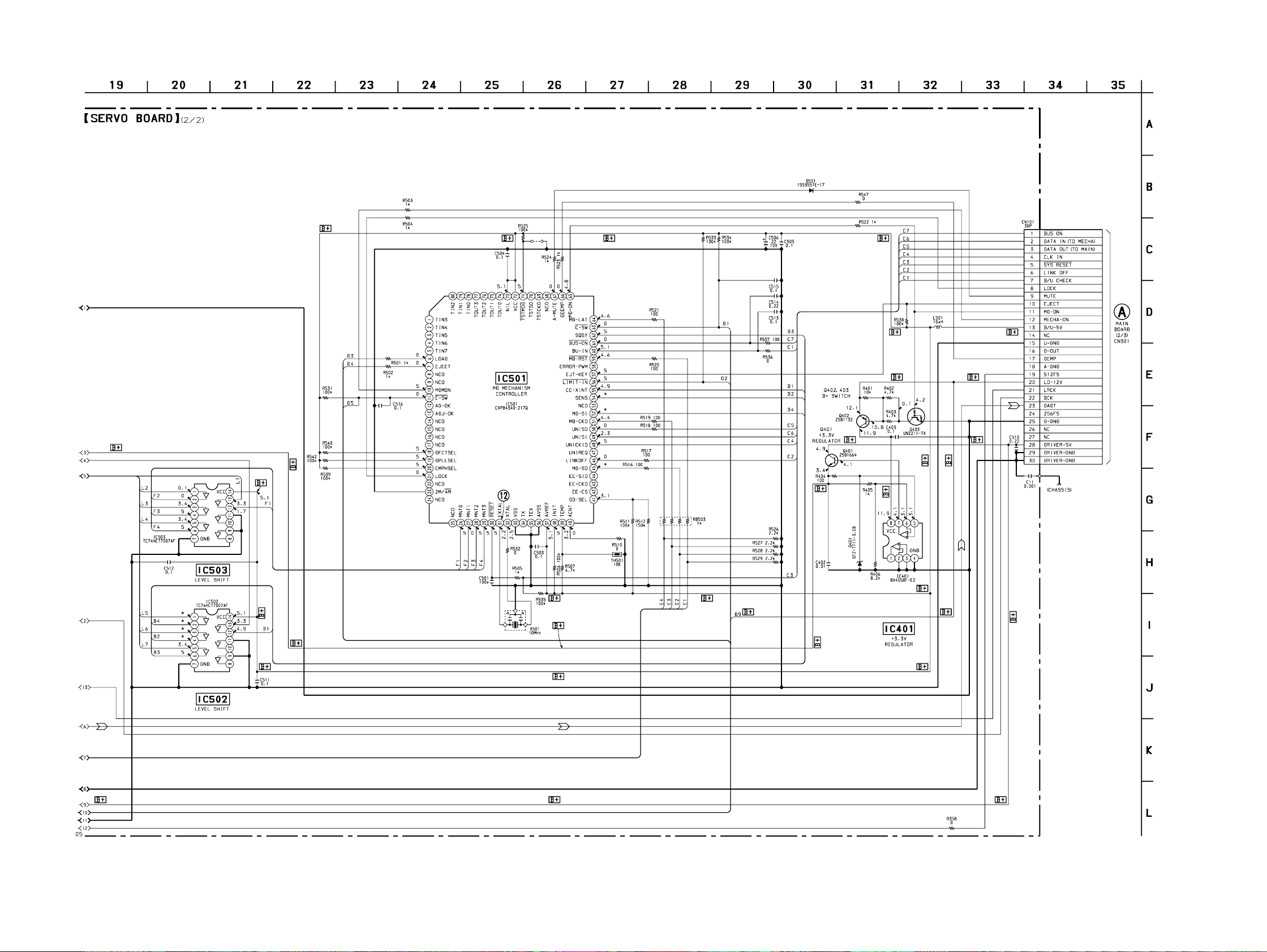
5-10. SCHEMATIC DIAGRAM – SERVO Board (2/2) –• See page 25 for Waveforms.
MDX-C8500R/C8500X
(Page
34)
• Voltages and waveforms are dc with respect to ground
under no-signal conditions.
no mark : MD PLAY
: Impossible to measure
∗
2929
Page 30
MDX-C8500R/C8500X
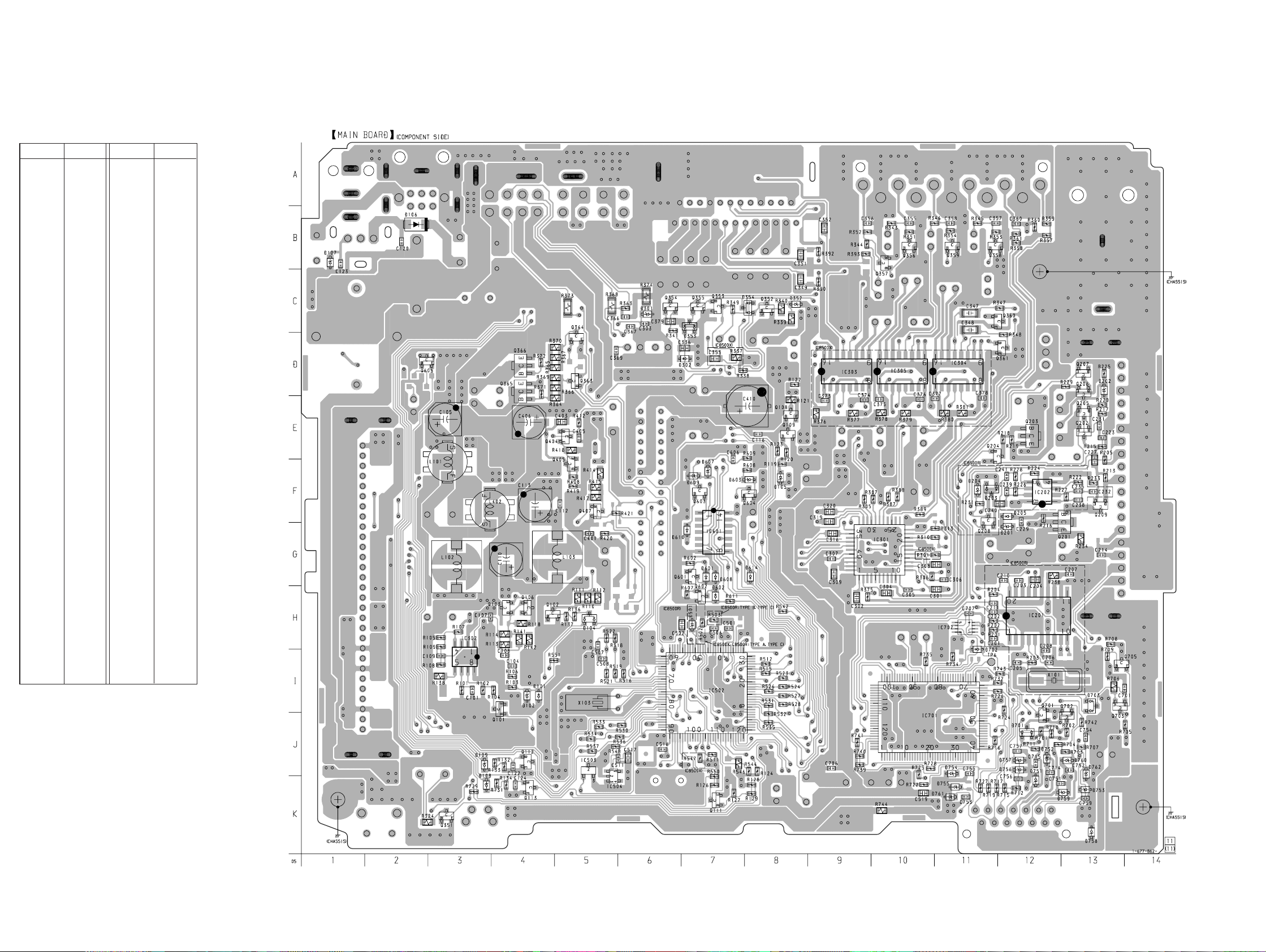
5-11. PRINTED WIRING BOARD – MAIN Board (Component Side) –• See page 24 for Circuit Boards Location.
• Semiconductor Location
Ref. No. LocationRef. No. Location
D101 I-4
D102 I-4
D104 H-5
D105 F-8
D106 B-2
D107 B-1
D108 K-3
D109 J-3
D201 G-12
D202 D-13
D203 F-11
D204 F-11
D205 F-12
D301 C-6
D302 D-7
D352 C-8
D353 C-7
D354 C-8
D501 H-7
D601 G-7
D602 H-7
D603 F-8
D607 F-7
D608 G-7
D609 F-7
D610 G-7
D614 G-8
D701 J-12
D702 I-11
D703 I-13
D751 K-12
D752 J-12
D753 K-13
D754 J-11
D755 K-11
D756 J-12
D757 J-12
D758 K-13
D759 K-13
D760 J-13
D761 K-11
D762 J-13
IC201 H-12
IC202 F-12
IC301 G-10
IC302 I-3
IC303 D-9
IC304 D-11
IC305 D-10
IC502 I-7
IC503 J-5
IC504 K-5
IC601 G-7
IC701 J-10
IC702 H-11
Q101 I-4
Q102 H-4
Q103 H-4
Q106 H-4
Q108 E-8
Q109 E-8
Q111 K-7
Q112 J-4
Q113 K-4
Q201 G-13
Q202 E-13
Q203 E-12
Q204 E-11
Q205 E-13
Q206 D-13
Q207 D-13
Q208 F-11
Q209 F-13
Q351 K-3
Q352 C-8
Q353 C-7
Q354 C-6
Q355 C-7
Q356 B-10
Q357 B-10
Q358 B-11
Q359 B-11
Q360 C-12
Q361 D-12
Q363 D-5
Q364 D-5
Q365 D-4
Q366 D-4
Q404 E-5
Q405 F-5
Q407 F-5
Q601 G-7
Q602 H-7
Q603 F-7
Q604 F-8
Q605 D-2
Q701 J-12
Q702 J-13
Q703 I-13
Q705 I-13
3030
Page 31

5-12. PRINTED WIRING BOARD – MAIN Board (Conductor Side) –• See page 24 for Circuit Boards Location.
65
8 7
321
(FRONT VIEW)
MDX-C8500R/C8500X
4
RL+ RL–
CN101
GRN
TO
ANT REM
WHT
GRY
VIO
WHT
GRN
VIO
GRY
BLU
RED
BLK
RED
BLU
FL+ FL–
FR+ FR–
RR+ RR–
1 9
2 10
3 11
4 12
5 13
6 14
7 15
8 16
ACC GND
NC BATT
NC NC
GRN/BLK
WHT/BLK
GRY/BLK
VIO/BLK
WHT/BLK
GRN/BLK
VIO/BLK
GRY/BLK
LIGHT BLU
ATT
BLU/WHT
AMP REM
ORG/WHT
YEL
BLK
ILL
ORG/WHT
YEL
• Semiconductor
Location
Ref. No. Location
D103 G-3
D355 C-7
(C8500R)
D356 C-7
D357 C-6
D358 C-6
D359 B-8
D360 B-7
D361 B-8
D362 B-8
D363 C-2
D502 J-8
D604 C-2
D605 B-2
D606 C-2
D611 D-1
D612 D-2
D613 D-2
IC351 B-7
Q104 F-4
Q105 G-3
Q107 E-8
Q110 B-1
Q401 E-4
Q406 F-5
Q704 J-13
(Page
36)
1 9
2 10
3 11
4 12
5 13
6 14
7 15
8 16
WHT/BLK
WHT
GRN/BLK
GRN
VIO/BLK
VIO
GRY/BLK
GRY
LIGHT BLU
BLU/WHT
ORG/WHT
BLU
RED
YEL
BLK
(C8500X)
FRONT LCH (–)
FRONT LCH (+)
REAR LCH (–)
REAR LCH (+)
REAR RCH (–)
REAR RCH (+)
FRONT RCH (–)
FRONT RCH (+)
ATT
AMP REM
ILL IN
ANT REM
ACC
BATT
GND
(Page 38)
(Page 26)
3131
Page 32

MDX-C8500R/C8500X
5-13. SCHEMATIC DIAGRAM – MAIN Board (1/4) – • See page 25 for Waveforms. • See page 42 for IC Block Diagrams.
(Page 37)
(Page
33)
• Voltages and waveforms are dc with respect to ground
under no-signal (detuned) conditions.
no mark : FM
( ) : AM (MW)
[]: LW
(Page 34)
3232
Page 33

5-14. SCHEMATIC DIAGRAM – MAIN Board (2/4) –• See page 42 for IC Block Diagrams.
MDX-C8500R/C8500X
(Page
32)
(Page 34)
(Page 35)
• Voltages are dc with respect to ground under no-signal
(detuned) conditions.
no mark : FM
3333
Page 34

MDX-C8500R/C8500X
5-15. SCHEMATIC DIAGRAM – MAIN Board (3/4) –• See page 25 for Waveforms. • See page 42 for IC Block Diagrams.
(Page 32)
(Page
33)
(Page
29)
(Page
35)
• Voltages and waveforms are dc with respect to ground
under no-signal (detuned) conditions.
no mark : FM
( ) : AM (MW)
[]: LW
〈〈 〉〉 : MD PLAY
3434
Page 35

5-16. SCHEMATIC DIAGRAM – MAIN Board (4/4) –• See page 25 for Waveforms.
MDX-C8500R/C8500X
(Page 33)
(Page
34)
(Page
39)
• Voltages and waveforms are dc with respect to ground
under no-signal (detuned) conditions.
no mark : FM
3535
Page 36

MDX-C8500R/C8500X
5-17. PRINTED WIRING BOARD – DSO Board –• See page 24 for Circuit Boards Location.
• Semiconductor
Location
(Component Side)
Ref. No. Location
D804 B-5
IC801 A-2
IC803 B-2
IC806 B-1
IC809 B-5
Q801 A-3
(Page 31)
• Semiconductor
Location
(Conductor Side)
Ref. No. Location
D802 C-1
IC802 B-1
IC805 B-3
IC807 A-5
IC808 B-5
3636
Page 37

5-18. SCHEMATIC DIAGRAM – DSO Board –• See page 25 for Waveforms. • See page 42 for IC Block Diagrams.
MDX-C8500R/C8500X
(Page
32)
• Voltages and waveforms are dc with respect to ground
under no-signal conditions.
no mark : MD PLAY
: Impossible to measure
∗
3737
Page 38

MDX-C8500R/C8500X
5-19. PRINTED WIRING BOARD – SUB Board –• See page 24 for Circuit Boards Location.
(Page 31)
(Page 40)
3838
Page 39

5-20. SCHEMATIC DIAGRAM – SUB Board –
(Page 41)
MDX-C8500R/C8500X
(Page 35)
• Voltages are dc with respect to ground under no-signal
(detuned) conditions.
no mark : FM
3939
Page 40

MDX-C8500R/C8500X
5-21. PRINTED WIRING BOARD – KEY Board –• See page 24 for Circuit Boards Location.
• Semiconductor
Location
(Component Side)
Ref. No. Location
IC951 C-5
LED901 C-2
LED902 A-2
LED903 A-3
LED904 C-3
LED910 B-12
LED911 B-12
LED912 A-12
LED913 A-5
LED914 B-5
LED915 B-5
• Semiconductor
Location
(Conductor Side)
Ref. No. Location
D901 B-13
D902 C-11
D903 C-11
D904 C-11
D951 C-5
D952 B-10
D954 B-10
IC901 B-8
Q901 A-3
Q902 A-3
Q903 A-5
(Page 38)
4040
Page 41

5-22. SCHEMATIC DIAGRAM – KEY Board –• See page 25 for Waveforms.
MDX-C8500R/C8500X
(Page
39)
• Voltages and waveforms are dc with respect to ground
under no-signal (detuned) conditions.
no mark : FM
4141
Page 42

• IC Block Diagrams
– SERVO Board –
IC301 CDX2652AR
EFMO
DVSS
TEST3
TEST2
99 98 97 96 95 94 93
EACH
BLOCK
EACH
BLOCK
SUBCODE
CLOCK
28
26
27
XBCK
DVDD
FS256
MNT0
MNT1
MNT2
MNT3
SWDT
SCLK
XLAT
SRDT
SENS
XRST
SQSY
DQSY
RECP
XINT
OSCI
OSCO
XTSL
DVSS
DIN
DOUT
ADDT
DADT
LRCK
100
1
2
MONITOR
CONTROL
3
4
5
6
CPU I/F
7
8
9
10
11
PROCESSOR
12
13
14
15
TX
16
17
GENERATOR
18
19
NC
20
21
22
23
24
25
TEST1
FGIN
SPINDLE
SERVO
DECODER
EACH
BLOCK
SPFD
ADIP
SPRD
DIGITAL
AUDIO
I/F
SFDR91SRDR90FS489FRDR88FFDR87DVDD86TFDR85TRDR84LDDR83APCREF82DTRF81CKRF80XLRF79F0CNT78ADFG77APC76DCHG
92
PWM
GENERATOR
SERVO
DSP
SHOCK RESISTANT
MEMORY CONTROLLER
SAMPLING
RATE
CONVERTER
ATRAC
ENCODER/DECODER
ADDRESS/DATA BUS A00 - A11, D0 - D3
39
40
A1138A0837A0736A0635A0534A0433A1032A0031A0130A0229A03
CONVERTER
41
XOE
DVSS
42
A/D
43
XCAS
A09
44
XRAS
AUTO
SEQUENCER
EFM/ACIRC
XWE
ENCODER/
ANALOG
MUX
DECODER
COMP
IC302 CXA2523AR
MORFO47MORFI46RFO45OPN
48
–
+
RFA1
+
–
75
AUX2
74
TE
73
SE
72
AVSS
71
ADRB
70
ADRT
69
AVDD
68
ADIO
67
VC
66
AUX1
65
FE
64
ABCD
63
BOTM
62
PEAK
61
CLTV
60
FILO
PLL
59
FILI
58
PCO
57
PDO
56
AVSS
55
RFI
54
BIAS
53
AVDD
52
ASYI
51
ASYO
50
49D348D247D046D145
MVCI
1I
2J
CVB
GSW
+
–
+
–
+
–
+
–
+
–
+
–
+
–
IV
+
–
3VC
4A
IVR
5B
IVR
6C
IVR
7D
IVR
8E
IVR
9F
IVR
10PD
11APC
12APCREF
RFA2
–
–
–
–
–
–
–
AA
BB
CC
DD
EE
FF
+
1
2
1
2
GRVA
EBAL
–
HLPT
OFST
GRV
+
–
+
–
FBAL
OPO43ADDC42COMPP41COMPO40AGCI39RF AGC38RF37PEAK
44
USROP
EE'
–
–
–
–
+
+
–
–
–
–
+
+
AUXSW
–1
–2
–2
–1
ESW
FF'
+
–
DECODE
–
+
–
+
BPF3T
BPF22
WBL
WBL
RFA3
PTGR
PBSW
ABCDA
FEA
ATA
EFB TESW
COMMAND
SCRI - PARA
RF AGC EQ
USRC
PEAK
BOTTOM
WBL
ADIP
PTGR
PEAK3T
P-P
PBH
AGC
WBL
3T
EQ
BGR
VREF
3T
3T WBL
DET
–1
–2
–1
–2
TEMP
DET
EQ
AUX
SW
BPFC
SEA
TEA
VI CONV
TG
TG
36
BOTM
35
ABCD
34
FE
33
AUX
32 ADFG
31 ADAGC
30 ADIN
29 ADFM
28 SE
27 CSLED
26 TE
25 WBLADJ
14
13
GND
TEMPI
15
TEMPR
SWDT
SCLK
XLAT
XSTBY
F0CNT
VREF
EQADJ
3TADJ
VCC
24
23
22
21
20
19
18
17
16
4242
Page 43

IC303 BH6511FS
CAPA–
CAPA+
IN2R
IN2F
VM2
OUT2F
PGND2
OUT2R
VM12
OUT1R
PGND1
OUT1F
VM1
32 31 30 29 28 27 26 25 24 23 22 21 20 19 18 17
IN4F
AMP
AMP
VM4
INTERFACE
CHARGE
PUMP.
OSC
INTERFACE
1 2 3 4 5 6 7 8 9 10 11 12 13 14 15 16
VG
GND
IN4R
OUT4F
AMP
PGND4
OUT4R
VM34
AMP
OUT3R
PGND3
AMP
AMPAMPAMP
OUT3F
INTERFACE
PREDRIVEPREDRIVE
PREDRIVEPREDRIVE
INTERFACE
VM3
IC305 BA6287F
1
OUT1
8
GND
IN1F
IN3F
IN1R
IN3R
V
PSB
DD
V
DD
PSB
2
VM
DRIVER DRIVER
TSD
3
VCC
FIN
POWER
SAVE
4
CONTROL LOGIC
IC307 MN41V4400TT-08S
TIMING
GENERATOR
DQ1
1
2
DQ2
3
WE
4
RAS
5
A9
NC
6
7
NC
8
NC
9
A0
10
A1
11
A2
12
A3
ADDRESS BUFFERS
COLUMN
ROW
INTERNAL
ADDRESS
COUNTER
ROW
DECODERS
REFRESH
CONTROL
CLOCK
WORD
DRIVERS
7
OUT2
6
VREF
5
RIN
COLUMN
DECODERS
SENSE
AMPLIFIERS
MEMORY
CELLS
TIMING
GENERATOR
I/O
SELECTOR
INPUT
BUFFERS
DATA BUS
WRITE
CLOCK
GENERATOR
OUTPUT
BUFFERS
VSS
26
25
DQ4
DQ3
24
23
CAS
22
OE
NC
21
20
NC
NC
19
A8
18
A7
17
16
A6
A5
15
A4
14
VCC
13
43
Page 44

– MAIN Board –
IC201 SAA6588T/V2-118
LVIN
20
MULTI
PATH
DETECTOR
2
1
MRO
MPTH
CIN
19
CLOCKED
COMPARATOR
RDS/RDBS
DEMODULATOR
TEST
CONTROL
3
TCON
SCOUT
18
BAND-PASS FILTER
OSCILLATOR
& CLOCK
4 5
OSCO
57kHz
8th ORDER
RDS/RDBS
DECODER
6
OSCI
VSSD
CLOCK
7
VDDD
17
DATA
8
VREF
MPX
SIGNAL QUALITY
DECODER
445
INTERFACE
REGISTER
DAVN
VDDA
VSSA
14
15
POWER SUPPLY
& RESET
CLOCK
DATA
AFIN
1316
IIC BUS SLAVE
TRANSCEIVER
9 10
SCL
SDA
PAUSE
DETECTOR
MAD
PSWN
11
12
IC302 TL5001CD
FEED BACK
INPUTSCP
REFERENCE
VOLTAGE
+
–
S.C.P.
COMPARATOR 1
ERROR
AMP
+
–
5
SWITCH
'ON'
AT
'H'
COMPARATOR
COMPARATOR 2
6 7
CONTROL
DEAD-TIME
U.V.L.O
OSC
–
+
PWM
–
+
S.C.P.
VCC
RT
DEAD-TIME
COMPARATOR
–
+
S.C.P.
LATCH
IC303 – 305 NJM2160AM-TE2
1
OUT
1234
8
GND
VCCL
INL
SVRL
INML
INMR
SVRR
INR
VCCR
2
3
4
5
6
7
8
BUFFER
BUFFER
REFERENCE
REFERENCE
BUFFER
BUFFER
VCCL
VCCL
VCCR
VCCR
LIFT
AMP
SIGNAL
AMP
SIGNAL
AMP
LIFT
AMP
CL+
16
CL–
15
LGND
14
OUTL
13
12
OUTR
RGND
11
CR–
10
9
CR+
44
Page 45

IC301 TDA7402TR
34
ACINLF
35
SWINR
36
SWINL
37
ACOUTR
38
ACOUTL
39
CREF
LP
HP
BASS
TREBLE
VOLUME
SOFTMUTE
LOUDNESS
MUX
40
+
IN-GAIN
+AUTO ZERO
MAIN SOURCE
SELECTOR
MD1
41
MD1G
MD2
MD2G
MAIN
42
43
PHONO
44
MAIN CH0 AUX
1 2 3 4 5 6 7 8 9 10 11
SEL
SER
ACINLR
ACINRF
ACINRR
33 32 31 30 29 28 27 26 25
LOUDNESS
IN-GAIN
MUTE
SELECTOR
FD2L–
FD2R+
FD2R–
FRONT
REAR
SW
FM
AM
AM
VOICE
BANDPASS
COMPANDER
MIXING
SELECTOR
MULTIPLEXER
FD1L+
FD1L–
ACIN
MAIN
INPUT
FD1R+
SECOND
FD1R–
OUTPUT
SELECTOR
SECOND SOURCE
FD2L+
MONO-
FADER
DIGITAL CONTROL IIC-BUS
OUTLF
MONO-
FADER
OUTLR
MIXER
MONO-
FADER
BEEP
AM/FM
NOISE BLANKER
OUTRF
OUTRR
MONO-
FADER
HIGH-CUT
S&H
25kHz
LP
DEMODULATOR
+STEREO ADJUST
+STEREO BLAND
PILOT
CANCELATION
OUTSWL
MONO-
FADER
SUBWOOFER
+PHASE
CONTROL
PIL DET
PLL
MONOFADER
OUTSWR
SUPPLY
PULSE
FORMER
QUAL
MULTIPATH
DETECTOR
D/A
CONVERTER
80kHz
LP
OUTSSL
24 23
OUTSSR
22
VDD
21
SCL
20
SDA
19
GND
18
SM
17
QUAL
16
MPOUT
15
MPIN
14
LEVEL
13
MPX
12
AMIF
45
Page 46

IC601 BA8270F-E2
BUS ON
1
2
RST
BATT
3
4
CLK
5
VREF
6
DATA
GND
7 8
BUS ON
SWITCH
RESET
SWITCH
BATTERY
SWITCH
– DSO Board –
IC805 CXD2726Q-4
LRCK
XMST
VDD3
AVSP
XPLLEN
80 79 78 77 76 75 74 73 72 71 70 69 68 67 66 65 64 63 62 61 60 59 58 57 56 55 54 53 52 51
PLCLK
XECKSTP
AVDP
VSS4
T. P
T. P
T. P
T. P
T. P
T. P
T. P
T. P
T. P
T. P
VDD4
AVSD
T. P
T. P
T. P
AVDD
81
82
83
84
85
86
87
88
89
90
91
92
93
94
95
96
97
98
99
100
COMPUTER
SIN
BCK
SERIAL DATA
MICRO
I/F
512kbit
DELAY
RAM
VCC
14
13
RST
BUS ON
12
CLK IN
11
BU IN
10
DATA IN
9
DATA OUT
SI1
SI2
SI3
I/F
GENERATOR/
TIMING CIRCUIT
SOUT
DSP
CLOCK
PLL
SO3
SO2
SO1
RVDT
XS24
VDD2
VSS3
SERIAL
DATA
I/F
DIGITAL
FILTER
CLOCK
GENERATOR/
TIMING CIRCUIT
XLAT
TRDT
REDY
SCK
BFOT
XRST
ADC2
ADC1
DAC6
DAC5
DAC4
DAC3
DAC2
DAC1
VSS2
AVD6
AOUTL3
AVD4
AOUTR3
AVS4
50
AVS6
49
AVD2
48
AVS2
47
RREF
46
RIN
45
AVS8
44
AVD8
43
AOUTR2
42
AVSX
41
–
+
–
+
–
+
–
+
–
+
–
+
40
39
38
37
36
35
34
33
32
31
XTLI38
XTLO38
AVDX
AOUTL2
AVD7
AVS7
LIN
LREF
AVS1
AVD1
AVS5
46
1 2 3 4 5 6 7 8 9 10 11 12 13 14 15 16 17 18 19 20 21 22 23 24 25 26 27 28 29 30
T. P
T. P
T. P
T. P
T. P
T. P
T. P
T. P
T. P
T. P
T. P
T. P
T. P
VSS1
T. P
TST0
TST1
TST2
TST3
TST4
TST5
JPE1
JPE2
JPE3
VDD1
AVS3
AVD3
AOUTL1
AOUTR1
AVD5
Page 47

5-23. IC PIN FUNCTION DESCRIPTION
• SERVO BOARD IC301 CXD2652AR
(DIGITAL SIGNAL PROCESSOR, DIGITAL SERVO PROCESSOR, EFM/ACIRC ENCODER/DECODER,
SHOCK PROOF MEMORY CONTROLLER, ATRAC ENCODER/DECODER, 2M BIT D-RAM)
Pin No. Pin Name I/O Description
1 MNT0 O
2 MNT1 O
3 MNT2 O
4 MNT3 O
5SWDTI
6 SCLK I
7 XLAT I
8 SRDT O (3)
9 SENS O (3)
10 XRST I Reset signal input from the MD mechanism controller (IC501) “L”: reset
11
12
13 RECP I
14 XINT O Interrupt status output to the MD mechanism controller (IC501)
15 TX I
16 OSCI I System clock signal (512Fs=22.5792 MHz) input from the oscillator circuit
17 OSCO O System clock signal (512Fs=22.5792 MHz) output terminal Not used (open)
18 XTSL I
19 RVDD — Power supply terminal (+3.3V) (digital system)
20 RVSS — Ground terminal (digital system)
21
22
23
24
25
26
27 FS256 O
28 DVDD — Power supply terminal (+3.3V) (digital system)
29 to 32
33
34 to 38
39
40 DVSS — Ground terminal (digital system)
41 XOE O Output enable signal output to the D-RAM (IC307) “L” active
42 XCAS O Column address strobe signal output to the D-RAM (IC307) “L” active
43 A09 O Address signal output to the D-RAM (IC307)
44 XRAS O Row address strobe signal output to the D-RAM (IC307) “L” active
45 XWE O Write enable signal output to the D-RAM (IC307) “L” active
SQSY O
DQSY O
DIN I Digital audio signal input terminal when recording mode Not used (fixed at “L”)
DOUT O Digital audio signal output terminal when playback mode Not used (open)
ADDT I Recording data input terminal Not used (fixed at “L”)
DADT O Playback data output to the CXD2726Q (IC805)
LRCK O L/R sampling clock signal (44.1 kHz) output to the CXD2726Q (IC805)
XBCK O Bit clock signal (2.8224 MHz) output to the CXD2726Q (IC805)
A03 to A00 O Address signal output to the D-RAM (IC307)
A10 O
A04 to A08 O Address signal output to the D-RAM (IC307)
A11 O
Focus OK signal output to the MD mechanism controller (IC501)
“H” is output when focus is on (“L”: NG)
Track jump detection signal output to the MD mechanism controller (IC501)
Busy monitor signal output to the MD mechanism controller (IC501)
Spindle servo lock status monitor signal output to the MD mechanism controller (IC501)
Writing serial data signal input from the MD mechanism controller (IC501)
Serial data transfer clock signal input from the MD mechanism controller (IC501)
Serial data latch pulse signal input from the MD mechanism controller (IC501)
Reading serial data signal output to the MD mechanism controller (IC501)
Internal status (SENSE) output to the MD mechanism controller (IC501)
Subcode Q sync (SCOR) output to the MD mechanism controller (IC501)
“L” is output every 13.3 msec Almost all, “H” is output
Digital In U-bit CD format subcode Q sync (SCOR) output terminal
“L” is output every 13.3 msec Almost all, “H” is output Not used (open)
Laser power selection signal input terminal
“L”: playback mode, “H”: recording mode (fixed at “L” in this set)
Recording data output enable signal input terminal
Writing data transmission timing input (Also serves as the magnetic head on/off output)
Not used (fixed at “L”)
Input terminal for the system clock frequency setting
“L”: 45.1584 MHz, “H”: 22.5792 MHz (fixed at “H” in this set)
Clock signal (11.2896 MHz) output terminal Not used (open)
Address signal output to the external D-RAM Not used (open)
Address signal output to the external D-RAM Not used (open)
47
Page 48

Pin No. Pin Name I/O Description
46 D1 I/O
47 D0 I/O
48 D2 I/O
49 D3 I/O
50 MVCI I Digital in PLL oscillation input from the external VCO Not used (fixed at “L”)
51 ASYO O Playback EFM full-swing output terminal
52 ASYI I (A) Playback EFM asymmetry comparator voltage input terminal
53 AVDD — Power supply terminal (+3.3V) (analog system)
54 BIAS I (A) Playback EFM asymmetry circuit constant current input terminal
55 RFI I (A) Playback EFM RF signal input from the CXA2523AR (IC302)
56 AVSS — Ground terminal (analog system)
57 PDO O (3) Phase comparison output for clock playback analog PLL of the playback EFM Not used (open)
58 PCO O (3) Phase comparison output for master clock of the recording/playback EFM master PLL
59 FILI I (A) Filter input for master clock of the recording/playback master PLL
60 FILO O (A) Filter output for master clock of the recording/playback master PLL
61 CLTV I (A) Internal VCO control voltage input of the recording/playback master PLL
62 PEAK I (A) Light amount signal (RF/ABCD) peak hold input from the CXA2523AR (IC302)
63 BOTM I (A) Light amount signal (RF/ABCD) bottom hold input from the CXA2523AR (IC302)
64 ABCD I (A) Light amount signal (ABCD) input from the CXA2523AR (IC302)
65 FE I (A) Focus error signal input from the CXA2523AR (IC302)
66 AUX1 I (A) Auxiliary signal (I
67 VC I (A) Middle point voltage (+1.65V) input from the CXA2523AR (IC302)
68 ADIO O (A) Monitor output of the A/D converter input signal Not used (open)
69 AVDD — Power supply terminal (+3.3V) (analog system)
70 ADRT I (A) A/D converter operational range upper limit voltage input terminal (fixed at “H” in this set)
71 ADRB I (A) A/D converter operational range lower limit voltage input terminal (fixed at “L” in this set)
72 AVSS — Ground terminal (analog system)
73 SE I (A) Sled error signal input from the CXA2523AR (IC302)
74 TE I (A) Tracking error signal input from the CXA2523AR (IC302)
75 AUX2 I (A) Auxiliary signal input terminal Light amount signal input from the CXA2523AR (IC302)
76 DCHG I (A) Connected to the +3.3V power supply
77 APC I (A) Error signal input for the laser automatic power control Not used (fixed at “L”)
78 ADFG I ADIP duplex FM signal (22.05 kHz ± 1 kHz) input from the CXA2523AR (IC302)
79 F0CNT O Filter f0 control signal output terminal Not used (open)
80 XLRF O Serial data latch pulse signal output terminal Not used (open)
81 CKRF O Serial data transfer clock signal output terminal Not used (open)
82 DTRF O Writing serial data output terminal Not used (open)
83 APCREF O
84 LDDR O PWM signal output for the laser automatic power control Not used (open)
85 TRDR O Tracking servo drive PWM signal (–) output to the BH6511FS (IC303)
86 TFDR O Tracking servo drive PWM signal (+) output to the BH6511FS (IC303)
87 DVDD — Power supply terminal (+3.3V) (digital system)
88 FFDR O Focus servo drive PWM signal (+) output to the BH6511FS (IC303)
Two-way data bus with the D-RAM (IC307)
3
signal/temperature signal) input terminal Not used (fixed at “H”)
Control signal output to the reference voltage generator circuit for the laser automatic power
control
48
Page 49

Pin No. Pin Name I/O Description
89 FRDR O Focus servo drive PWM signal (–) output to the BH6511FS (IC303)
90 FS4 O Clock signal (176.4 kHz) output terminal (X’tal system) Not used (open)
91 SRDR O Sled servo drive PWM signal (–) output to the BH6511FS (IC303)
92 SFDR O Sled servo drive PWM signal (+) output to the BH6511FS (IC303)
93 SPRD O Spindle servo drive PWM signal (–) output to the BH6511FS (IC303)
94 SPFD O Spindle servo drive PWM signal (+) output to the BH6511FS (IC303)
95
96
97
98
99 DVSS — Ground terminal (digital system)
100 EFMO O EFM signal output terminal when recording mode Not used (open)
* I (A) for analog input, O (3) for 3-state output, and O (A) for analog output in the column I/O.
FGIN I Not used (fixed at “L”)
TEST1 I
TEST2 I Input terminal for the test (fixed at “L”)
TEST3 I
49
Page 50

• SERVO BOARD IC302 CXA2523AR (RF AMP, FOCUS/TRACKING ERROR AMP)
Pin No. Pin Name I/O Description
1II
2JI
3VCO
4 to 9 A to F I
10 PD I
11 APC O
12 APCREF I
13 GND —
14 TEMPI I
15
16 SWDT I
17 SCLK I
18 XLAT I
19 XSTBY I
20 F0CNT I
21 VREF O
22 EQADJ I
23 3TADJ I
24 VCC —
25 WBLADJ I
26 TE O
27 CSLED I
28 SE O
29 ADFM O
30 ADIN I
31 ADAGC I
32 ADFG O
33 AUX O
34 FE O
35 ABCD O
36 BOTM O
37 PEAK O
38 RF O
39 RFAGC I
40 AGCI I
41 COMPO O
42 COMPP I
43 ADDC I
44 OPO O
45 OPN I
46 RFO O
47 MORFI I
48 MORFO O
TEMPR O
I-V converted RF signal I input from the optical pick-up block detector
I-V converted RF signal J input from the optical pick-up block detector
Middle point voltage (+1.65V) generation output terminal
Signal input from the optical pick-up detector
Light amount monitor input from the optical pick-up block laser diode
Laser amplifier output terminal to the automatic power control circuit
Reference voltage input terminal for setting laser power
Ground terminal
Connected to the temperature sensor Not used (open)
Output terminal for a temperature sensor reference voltage Not used (open)
Writing serial data input from the MD mechanism controller (IC501)
Serial data transfer clock signal input from the MD mechanism controller (IC501)
Serial data latch pulse signal input from the MD mechanism controller (IC501)
Standby signal input terminal “L”: standby (fixed at “H” in this set)
Center frequency control voltage input terminal of internal circuit (BPF22, BPF3T, EQ) input
terminal
Reference voltage output terminal Not used (open)
Center frequency setting terminal for the internal circuit (EQ)
Center frequency setting terminal for the internal circuit (BPF3T)
Power supply terminal (+3.3V)
Center frequency setting terminal for the internal circuit (BPF22)
Tracking error signal output to the CXD2652AR (IC301)
Connected to the external capacitor for low-pass filter of the sled error signal
Sled error signal output to the CXD2652AR (IC301)
FM signal output of the ADIP
Receives a ADIP FM signal in AC coupling
Connected to the external capacitor for ADIP AGC
ADIP duplex signal (22.05 kHz ± 1 kHz) output to the CXD2652AR (IC301)
Auxiliary signal (I
Focus error signal output to the CXD2652AR (IC301)
Light amount signal (ABCD) output to the CXD2652AR (IC301)
Light amount signal (RF/ABCD) bottom hold output to the CXD2652AR (IC301)
Light amount signal (RF/ABCD) peak hold output to the CXD2652AR (IC301)
Playback EFM RF signal output to the CXD2652AR (IC301)
Connected to the external capacitor for RF auto gain control circuit
Receives a RF signal in AC coupling
User comparator output terminal Not used (open)
User comparator input terminal Not used (fixed at “L”)
Connected to the external capacitor for cutting the low band of the ADIP amplifier
User operational amplifier output terminal Not used (open)
User operational amplifier inversion input terminal Not used (fixed at “L”)
RF signal output terminal
Receives a MO RF signal in AC coupling
MO RF signal output terminal
3
signal/temperature signal) output terminal Not used (open)
50
Page 51

• SERVO BOARD IC501 CXP84340-217Q (MD MECHANISM CONTROLLER)
Pin No. Pin Name I/O Description
1 to 5 TIN3 to TIN7 I/O
6LOAD
7 EJECT O
8, 9 NCO O
10 MDMON O
11 E-SW I
12 AG-OK O
13 ADJ-OK O
14 to 17 NCO O
18 DFCTSEL I
19 DPLLSEL I
20 EMPHSEL I
21 LOCK O
22 NCO O
23 2M/4M I
24, 25 NCO O
26
27 MNT1 I
28 MNT2 I
29 MNT3 I
30 RESET I
31 EXTAL
32 XTAL
33 VSS
34 TX
35 TEX
36 AVSS
37 AVREF
38 INIT
39 TEMP
40 ACNT
41 DO-SEL
42 EE-CS
43 EE-CKO
44 EE-SIO I/O
45 MD-SO O
MNT0
Input of the 4×8 matrix test keys (“L” is always output, except in test mode) Not used (open)
O Loading motor control signal output to the motor driver (IC305) “H” active *1
Loading motor control signal output to the motor driver (IC305) “H” active *1
Not used (open)
Power supply on/off control signal output of the MD mechanism deck section main power supply
and loading motor drive (IC305) power supply “H”: power on
Inputs the disc loading completion detect switch detection signal
“L”: When completed of the disc loading operation
Output of aging status in test mode “L”: under aging, “H”: aging completed Not used (open)
Output of status when aging completed in test mode “L”: aging NG, “H”: aging OK
Not used (open)
Not used (open)
Select whether defect function is used for the CXD2652AR (IC301)
“L”: used this function , “H”: not used this function (fixed at “H” in this set)
Select whether digital PLL function is used for the CXD2652AR (IC301)
“L”: used this function , “H”: not used this function (fixed at “H” in this set)
Select whether emphasis signal output from pin or unilink data
“L”: outputs from both pin and unilink data, “H”: output from pin only (fixed at “H” in this set)
Mini-disc lock detection signal output terminal “H”: lock Not used
Not used (open)
Select whether D-RAM capacitance 2M bit or 4M bit “L”: 4M bit (external D-RAM) , “H”: 2M
bit (internal D-RAM of CXD2652AR) (fixed at “L” in this set)
Not used (open)
Focus OK signal input from the CXD2652AR (IC301)
I
“H” is input when focus is on (“L”: NG)
Track jump detection signal input from the CXD2652AR (IC301)
Busy monitor signal input from the CXD2652AR (IC301)
Spindle servo lock status monitor signal input from the CXD2652AR (IC301)
System reset signal input from the master controller (IC502), reset signal generator (IC503) and
reset switch (S101) “L”: reset
For several hundreds msec. after the power supply rises, “L” is input, then it changes to “H”
O Main system clock output terminal (10 MHz)
I Main system clock input terminal (10 MHz)
— Ground terminal
O Sub system clock output terminal (32.768 kHz) Not used (open)
I Sub system clock input terminal (32.768 kHz) Not used (fixed at “L”)
— Ground terminal (for A/D converter)
I Reference voltage input terminal (+5V) (for A/D converter)
I Initial reset signal input terminal (A/D input) (fixed at “H”)
I Temperature sensor (TH501) input terminal (A/D input)
Select the number of load/eject aging times (A/D input)
I
0H – 54H (30 times), 55H – OA9H (20 times), OAAH – OFFH (10 times)
I Select the digital output bits (A/D input)
O Chip select signal output to the external EEPROM device Not used (open)
O Serial data transfer clock signal output to the external EEPROM device Not used (open)
Two way data bus with the external EEPROM device Not used (open)
Writing serial data signal output to the CXD2652AR (IC301) and CXA2523AR (IC302)
51
Page 52

Pin No. Pin Name I/O Description
n
46 LINKOFF O
47 UNIREQ O
48 UNICKIO I/O
49 UNISI I
50 UNISO O
51 MD-CKO O
52 MD-SI I
53 NCO O
54 SENS I
55 CC-XINT
56 LIMIT-IN
57 EJT-KEY I
58 ERROR-PWM O
59 MD-RST O
60 BU-IN I
61 BUS-ON I
62 SQSY
63 C-SW I
64 MD-LAT O
65 MD-ON O
66 DEEMP O
67 A-MUTE O
68 NCO O
69 TSTCKO O
70 TSTSO O
71 TSTMOD I
72 VCC —
73 NIL I
74 to 77
78 to 80 TIN0 to TIN2 I/O
TOUT0 to TOUT3
Unilink on/off control signal output for the SONY bus “L”: link on, “H”: link off Not used
Data request signal output terminal (for SONY bus) “H”: request on Not used (open)
Serial clock signal input from the master controller (IC502) or serial clock signal output to the
SONY bus interface (IC601) and liquid crystal display drive controller (IC701) (for SONY bus)
Serial data input from the SONY bus interface (IC601)
Serial data output to the SONY bus interface (IC601)
Serial data transfer clock signal output to the CXD2652AR (IC301) and CXA2523AR (IC302)
Reading serial data signal input from the CXD2652AR (IC301)
Not used (open)
Internal status (SENSE) input from the CXD2652AR (IC301)
I Interrupt status input from the CXD2652AR (IC301)
Detection input from the sled limit-in detect switch
I
The optical pick-up is inner position when “L”
Eject request signal input terminal “L”: eject on Not used (fixed at “H”)
PWM error monitor output terminal (C1and ATER is output when test mode) Not used (open)
Reset signal output to the CXD2652AR (IC301) and BH6511FS (IC303) “L”: reset
Battery detect signal input from the SONY bus interface (IC601) and battery check circuit
“H”: battery on
SONY bus on/off control signal input from the master controller (IC502) “L”: bus on
Subcode Q sync (SCOR) input from the CXD2652AR (IC301)
I
“L” is input every 13.3 msec Almost all, “H” is input
Inputs the disc loading start or disc eject completion detect switch detection signal
“L”: When start or eject completed of the disc loading operation
Serial data latch pulse signal output to the CXD2652AR (IC301) and CXA2523AR (IC302)
Power supply on/off control signal output of the MD mechanism deck section main power supply
“H”: power on
Emphasis on/off control signal output to the master controller (IC502) “H”: emphasis on
Audio muting on/off control signal output terminal “H”: muting on
Not used (open)
Output of clock signal for the test mode display Not used (open)
Output of data for the test mode display Not used (open)
Setting terminal for the test mode “L”: test mode, “H”: normal mode
Power supply terminal (+5V)
Not used (fixed at “H”)
O
Output of the 4×8 matrix test keys Not used (open)
Input of the 4×8 matrix test keys (“L” is always output, except in test mode) Not used (open)
*1 Loading motor (M903) control
Operatio
Terminal
LOAD (pin 6)
EJECT (pin 7)
IN OUT BRAKE STOP
“H”“L”“H”“L”
“L”“H”“H”“L”
52
Page 53

MAIN BOARD IC502 (MASTER CONTROLLER)
•
MB90574BPMT-G-263-BND (MDX-C8500X) MB90574BPMT-G-264-BND (MDX-C8500R)
Pin No. Pin Name I/O Description
1NCI
2 AMSIN I
3 AMSON O
4 SA LAT O
5 ATT
6 SYSRST O
7 F/R O
8VCC—
9 MTLIN I
10 T.ROM-SDA I/O Two-way data bus for tuner EEPROM with the FM/AM tuner unit (TUX201)
11
12 RX I
13 TX O
14 BUS-ON
15
16 NC O
17 UNISI
18 UNISO
19 UNICKO
20 IF-BW
21 SW SHIFT
22, 23 NC O
24
25
26
27
28
29
30 NC O
31 VOLATT
32 TUMUTE O
33
34 C —
T.ROM-SCL O
BEEP O Beep sound drive signal output terminal
SIRCS
DSPSI
DSPSO
DSPCKO
DSPPLL
DSPMST
VSS
Not used (fixed at “L”)
Input terminal of whether a music is present or not is detected at auto music sensor
“L”: music is not present, “H”: music is present Not used (fixed at “L”)
Tape auto music sensor control signal output terminal
“L” is output to lower the gain for audio level at FF/REW mode Not used (open)
Serial data latch pulse output for spectrum analyzer section to the liquid crystal display drive
controller (IC701)
O Audio line muting on/off control signal output terminal “H”: muting on
System reset signal output to the MD mechanism controller (IC501), liquid crystal display drive
controller (IC701) and SONY bus interface (IC601) “L”: reset
Tape detection signal output terminal “L”: reverse side, “H”: forward side Not used (open)
Power supply terminal (+5V)
Auto metal detection signal input terminal Not used (fixed at “L”)
Tuner EEPROM bus clock signal output to the FM/AM tuner unit (TUX201)
Input terminal at the flash memory data write mode
Front panel open/close detection signal input terminal
“L” is input when the front panel is closed
Output terminal at the flash memory data write mode
Display serial data output to the liquid crystal display driver (IC901)
Bus on/off control signal output to the MD mechanism controller (IC501), liquid crystal display
O
drive controller (IC701) and SONY bus interface (IC601) “L”: bus on
Not used (open)
I Serial data input from the SONY bus interface (IC601)
O Serial data output to the SONY bus interface (IC601)
Serial clock signal output to the MD mechanism controller (IC501), liquid crystal display drive
O
controller (IC701) and SONY bus interface (IC601)
Tuner wide/narrow select signal input terminal “L”: wide, “H”: narrow
I
Not used (fixed at “L”)
O Not used
Not used (open)
I
Sircs remote control signal input from the remote control receiver (IC951)
I
Serial data input from the CXD2726Q (IC805)
O
Serial data output to the CXD2726Q (IC805)
Serial data transfer clock signal output to the CXD2726Q (IC805) and liquid crystal display drive
O
controller (IC701)
PLL clock control signal output to the CXD2726Q (IC805)
O
At “L” is output: fixed at “L” is PLCLK (pin ia of IC805 CXD2726Q)
At “H” is output: PLL clock signal output to the PLCLK (pin ia of IC805 CXD2726Q)
Bit clock (BCK) and L/R sampling (LRCK) signal master/slave mode selection signal output to
O
the CXD2726Q (IC805) “L”: master mode, “H”: slave mode
Not used (open)
Pre amplifier muting on/off control signal output to the electrical volume (IC301)
O
“L”: muting on
Muting on/off control signal output of the FM/AM tuner signal “L”: muting on
—
Ground terminal
Connected to coupling capacitor for the power supply Not used (open)
53
Page 54

Pin No. Pin Name I/O Description
35 DSPLAT O
36 DSPRST O
37 ANT CUT
38 DVCC —
39 DVSS —
40, 41 NC O
42 AVCC
43 AVRH
44 AVRL
45 AVSS
46 KEYIN0
47 KEYIN1
48 RCIN0
49 DSTSEL I
50 QUALITY
51
52 MTP
53
54 VCC —
55 AMPON
56 NS-MASK O
57 MTLOUT O
58 REEL I
59 POS0 I
60 POS1 I
61 POS2 I
62 POS3 I
63 VSS —
64 NC I
65 F OSC I
66 LM-LOD O
67 CM ON O
68 TAPE ON O
69
70 I2C SDA I/O
71 I2C CKO O
FMAGC I
VSM I
FLASH-W
Serial data latch pulse output to the CXD2726Q (IC805)
Reset signal output to the CXD2726Q (IC805) “L”: reset
Tuner system power supply on/off control signal output terminal “H”: tuner power on
O
Not used (open)
Power supply terminal (+5V) (for D/A converter)
Ground terminal (for D/A converter)
Not used (open)
— Power supply terminal (+5V) (for analog system)
I Reference voltage (+5V) input terminal (for A/D converter)
I Reference voltage (0V) input terminal (for A/D converter)
— Ground terminal (for analog system)
Key input terminal (A/D input) (LSW901 to LSW908, S901 to S904)
OFF, SOURCE, SOUND EQ, MENU, PTY DSPL (MDX-C8500R), DSPL (MDX-C8500X),
I
LIST, ENTER, MODE, SEEK/AMS - . m + > M, DISC/PRST +, PRST/DISC - keys
input
Key input terminal (A/D input) (LSW751, LSW909 to LSW917)
I
Z, DSO, TA, AF, 6 to 3 SHUF 2, REP 1 keys input
(LSW910 TA, LSW911 AF: MDX-C8500R ONLY)
I Rotary remote commander key input terminal (A/D input)
Destination setting terminal (A/D input) “L”: MDX-C8500X/C8500R (TYPE A),
“M”: MDX-C8500R (TYPE C), “H”: MDX-C8500R (TYPE B)
I Noise level detection signal input at SEEK mode (A/D input)
FM AGC detection signal input from the FM/AM tuner unit (TUX201) (A/D input)
Multi-path detection signal input from the RDS decoder (IC201) (A/D input)
I
Used for the MDX-C8500R only (MDX-C8500X: Not used open))
FM and AM signal meter voltage detection input from the FM/AM tuner unit (TUX201)
(A/D input)
Power supply terminal (+5V)
Standby on/off control signal output terminal
O
“L”: standby mode, “H”: amplifier on
Discharge control signal output for the noise detection circuit “H”: discharge
Used for the MDX-C8500R only (MDX-C8500X: Not used open))
METAL output terminal (METAL on at “L” output) Not used (open)
Rotation detect signal input terminal Not used (fixed at “L”)
Tape position (EJECT/FF/REW/REV/
FWD mode) detect input from the tape
operation switch on the deck mechanism
Not used this function (fixed at “L”)
Ground terminal
Not used (fixed at “L”)
Frequency count terminal from power control (IC302)
Loading motor control signal output terminal “H” active
(For the loading direction and forward side operation) Not used (open)
Capstan/reel motor control signal output terminal “H”: motor on Not used (open)
Tape system power supply on/off control signal output terminal “H”: tape on Not used (open)
I
Internal flash memory data write mode detection signal input terminal Not used
Two-way data I2C bus with the FM/AM tuner unit (TUX201), RDS decoder (IC201) and
electrical volume (IC301) (RDS decoder is MDX-C8500R only)
I2C bus clock signal output to the FM/AM tuner unit (TUX201), RDS decoder (IC201) and
electrical volume (IC301) (RDS decoder is MDX-C8500R only)
POS0: “L”: EJECT mode, “H”: others mode
POS1: “L”: FF and FWD mode, “H”: others mode
POS2: “L”: REW mode, “H”: others mode
POS3: “L”: REV and EJECT mode, “H”: others mode
54
Page 55

Pin No. Pin Name I/O Description
72 RCIN1
73 X1A O
74 X0A I
75 DAVN I
76 CDMD ON I
77 BU-IN
78 DSPREADY
79 KEYACK
80 AD ON
81 ACCIN
82
83 PW-ON
84 TESTIN
85 RAMBU I
86 HSTX I
87 MD2 I
88 MD1 I
89 MD0 I
90 RESET I
91 VSS —
92 X0
93 X1
94 VCC —
95 ILLIN
96
97
98
99 to 102 NC O
103 4V SEL I
104 COL SEL
105 AMPATT
106 BOOT
107 DSP GAIN
108 NC O
109 XR CDMD
110 DSP ON
FLASH ON O
TELATT I Telephone detection signal input terminal At input of “H”, the signal is attenuated by –20 dB
EMPH I Emphasis control signal input from the MD Mechanism controller (IC501)
F CH O Frequency changing terminal from the power control (IC302) “H”: frequency change
I Rotary remote commander shift key input terminal
Sub system clock output terminal (32.768 kHz)
Sub system clock input terminal (32.768 kHz)
Data transmit completed detection signal input from the RDS decoder (IC201) “L” active
Used for the MDX-C8500R only (MDX-C8500X: Not used open))
CD/MD on/off control signal input from the MD mechanism controller (IC501)
Battery detection signal input from the SONY bus interface (IC601) and battery detect circuit
I
“L” is input at low voltage
Transfer enable signal input from the CXD2726Q (IC805)
I
“L”: transfer prohibition , “H”: transfer permission
Input of acknowledge signal for the key entry Acknowledge signal is input to accept function
I
and eject keys in the power off status On at input of “H”
A/D converter power control signal output terminal
O
When the KEYACK (pin ul) that controls reference voltage power for key A/D conversion input
is active, “L” is output from this terminal to enable the input
I Accessory detection signal input terminal “L”: accessory on
Power on/off control signal output of the illumination LED and liquid crystal display driver
(IC901) “H”: power on
O Main system power supply on/off control signal output terminal “H”: power on
I Setting terminal for the test mode “L”: test mode, Normally: fixed at “H”
Internal RAM reset detection signal input from the RN5VD33AA (IC504)
Input terminal to check that RAM data are not destroyed due to low voltage
This checking is made within 100 msec after reset
Hardware standby input terminal “L”: hardware standby mode Reset signal input in this set
Setting terminal for the CPU operational mode (fixed at “L” in this set)
Setting terminal for the CPU operational mode (fixed at “H” in this set)
Setting terminal for the CPU operational mode (fixed at “H” in this set)
System reset signal input from the reset signal generator (IC503) and reset switch (S101)
“L”: reset “L” is input for several 100 msec after power on, then it changes to “H”
Ground terminal
I Main system clock input terminal (3.68 MHz)
O Main system clock output terminal (3.68 MHz)
Power supply terminal (+5V)
Auto dimmer control illumination line detection signal input terminal
I
“L” is input at dimmer detection
Not used (open)
Input terminal of whether line driver is mounted or not is detected
“L”: line driver is not mounted (MDX-C8500R), “H”: line driver is mounted (MDX-C8500X)
Setting terminal for the illumination color
I
“L”: 2 color (MDX-C8500R), “H”: 1 (red) color (MDX-C8500X)
O Power amplifier muting on/off control signal output terminal “H”: muting on
O Serial data output to the liquid crystal display drive controller (IC701)
O Not used (open)
Not used (open)
Setting terminal for the internal mechanism tape or CD/MD
I
“L”: tape, “H”: CD/MD (fixed at “H” in this set)
O Power supply on/off control signal output for the CXD2726Q (IC805) “H”: DSP on
55
Page 56

Pin No. Pin Name I/O Description
111 CD MD
112
113
114
115 REIN1
116 REIN0
117 NOSE-SW I
118 DOORIND
119 VSS — Ground terminal
120 DOLBY O Dolby control terminal “H”: dolby on Not used (open)
NC I
TUNON O
NC I
Setting terminal for the internal mechanism CD or MD
I
“L”: CD, “H”: MD (fixed at “H” in this set)
Not used (fixed at “L”)
Tuner system power supply on/off control signal output terminal
“H”: tuner power on
Not used (fixed at “L”)
Dial pulse input of the rotary encoder (RE901) (A phase input)
I
(for VOLUME/BASS/TREBLE/BALANCE/FADER control)
Dial pulse input of the rotary encoder (RE901) (B phase input)
I
(for VOLUME/BASS/TREBLE/BALANCE/FADER control)
Front panel block remove/attach detection signal input from the nose detection switch (S102)
“L”: front panel is attached
LED drive signal output of the MD disc slot illumination and Z indicator (LED751, LSW751)
O
“H”: LED on “H” is output to turn on LED when front panel is opened
56
Page 57

• DSO BOARD IC805 CXD2726Q-4 (DIGITAL SIGNAL PROCESSOR, DIGITAL FILTER, D/A CONVERTER)
Pin No. Pin Name I/O Description
1 VSS1 —
2 to 15 T.P
16 to 21 TST0 to TST5 I
22 to 24 JPE1 to JPE3 I
25 VDD1 —
26 AVS3 —
27 AOUTL1 O
28 AVD3 —
29 AOUTR1 O
30 AVD5 —
31 AVS5 —
32 AVD1 —
33 AVS1 —
34 LREF O
35 LIN I
36 AVS7 —
37
38 AOUTL2 O
39 AVDX —
40 XTLO38 O
41 XTLI38 I
42 AVSX
43 AOUTR2
44 AVD8
45 AVS8
46 RIN
47 RREF
48 AVS2
49 AVD2
50 AVS6
51 AVD6
52 AOUTL3
53 AVD4
54 AOUTR3
55 AVS4 —
56 VSS2 —
57 XRST I
58 BFOT O
59 SCK I
AVD7
Ground terminal (digital system)
I Input terminal for the test (fixed at “L”)
Input terminal for the test (fixed at “L”)
External condition jump terminal “H”: condition jump (fixed at “L”)
Power supply terminal (+3.3V) (digital system)
Ground terminal (for D/A converter 1) (analog system)
D/A converter 1 (L-ch side) output terminal
Analog signal output for front side (L-ch side) output in this set
Power supply terminal (+3.3V) (for D/A converter 1) (analog system)
D/A converter 1 (R-ch side) output terminal
Analog signal output for rear side (L-ch side) output in this set
Power supply terminal (+3.3V) (for D/A converter 1) (analog system)
Ground terminal (for D/A converter 1) (analog system)
Power supply terminal (+3.3V) (for L-ch side A/D converter) (analog system)
Ground terminal (for L-ch side A/D converter) (analog system)
Connected to the bus control for A/D converter (for L-ch side)
A/D converter (L-ch side) analog input terminal
Tuner and bus audio input signal (L-ch side) in this set
Ground terminal (for D/A converter 2) (analog system)
—
Power supply terminal (+3.3V) (for D/A converter 2) (analog system)
D/A converter 2 (L-ch side) output terminal Not used (open)
Power supply terminal (+3.3V) (for master clock) (analog system)
System clock output terminal (16.9344 MHz)
System clock input terminal (16.9344 MHz)
— Ground terminal (for master clock) (analog system)
D/A converter 2 (R-ch side) output terminal
O
Analog signal output for sub woofer output in this set
— Power supply terminal (+3.3V) (for D/A converter 2) (analog system)
— Ground terminal (for D/A converter 2) (analog system)
A/D converter (R-ch side) analog input terminal
I
Tuner and bus audio input signal (R-ch side) in this set
O Connected to the bus control for A/D converter (for R-ch side)
— Ground terminal (for R-ch side A/D converter) (analog system)
— Power supply terminal (+3.3V) (for R-ch side A/D converter) (analog system)
— Ground terminal (for D/A converter 3) (analog system)
— Power supply terminal (+3.3V) (for D/A converter 3) (analog system)
D/A converter 3 (L-ch side) output terminal
O
Analog signal output for rear side (R-ch side) output in this set
— Power supply terminal (+3.3V) (for D/A converter 3) (analog system)
D/A converter 3 (R-ch side) output terminal
O
Analog signal output for front side (R-ch side) output in this set
Ground terminal (for D/A converter 3) (analog system)
Ground terminal (digital system)
System reset signal input from the master controller (IC502) “L”: reset
Master clock signal output terminal Not used (open)
Serial data transfer clock signal input from the master controller (IC502) and liquid crystal display
drive controller (IC701)
57
Page 58

Pin No. Pin Name I/O Description
60 REDY O
61 TRDT O
62 XLAT I
63 RVDT I
64 XS24 I
65 VDD2 —
66 VSS3 —
67 to 69 SO1 to SO3 O
70 SOUT O
71 SI1 I
72, 73 SI2, SI3 I
74 SIN I
75 BCK I
76 LRCK I
77 XMST I
78 VDD3 —
79 AVSP —
80 XPLLEN I
81 PLCLK O
82 XECKSTP I
83 AVDP —
84 VSS4 —
85 to 94 T.P
95 VDD4 —
96 AVSD —
97 to 99 T.P
100 AVDD —
Transfer enable signal output to the master controller (IC502)
“L”: transfer prohibition
Serial data output to the master controller (IC502) and liquid crystal display drive controller
(IC701)
Serial data latch pulse input from the master controller (IC502)
Serial data input from the master controller (IC502)
Serial data 24/32 bit slot selection signal input terminal
“L”: 24 bit slot, “H”: 32 bit slot (validity at slave mode) (fixed at “H” in this set)
Power supply terminal (+3.3V) (digital system)
Ground terminal (digital system)
Serial data output terminal Not used (open)
Serial data output terminal Not used (open)
Serial data input from the CXD2652AR (IC301)
Serial data input terminal Not used (fixed at “L”)
Serial data input terminal Not used (fixed at “L”)
Bit clock signal (2.8224 MHz) input from the CXD2652AR (IC301)
L/R sampling clock signal (44.1 kHz) input from the CXD2652AR (IC301)
Bit clock (BCK) and L/R sampling clock (LRCK) signal master/slave mode selection signal input
from the master controller (IC502) “L”: master mode, “H”: slave mode
Power supply terminal (+3.3V) (digital system)
Ground terminal (PLL system)
PLL enable signal input terminal Normally: fixed at “L”
PLL clock signal output terminal (22.5792 MHz)
PLL clock output control signal input from the master controller (IC502)
At “L” is input: fixed at “L” is PLCLK (pin ia)
At “H” is input: PLL clock signal output from the PLCLK (pin ia)
Power supply terminal (+3.3V) (PLL system)
Ground terminal (digital system)
I Input terminal for the test Normally: fixed at “L”
Power supply terminal (+3.3V) (digital system)
Ground terminal (for D-RAM)
I Input terminal for the test Normally: fixed at “L”
Power supply terminal (+3.3V) (for D-RAM)
58
Page 59

#10
#10
#10
#1
#1
Front panel section
1
5
6
7
8
#12
#3
#4
#4
#4
#3
#10
#10
#10
#3
#2
F1
4
3
2
9
12
24
25
26
27
11
15
16
21
22
18
19
A
B
A
B
14
13
MG-164NV-138
17
23
not
supplied
TUX201
SECTION 6
EXPLODED VIEWS
Ver 1.2
NOTE:
• -XX and -X mean standardized parts, so they
may have some difference from the original
one.
• Color Indication of Appearance Parts
Example:
KNOB, BALANCE (WHITE) . . . (RED)
↑↑
Parts Color Cabinet's Color
(1) GENERAL SECTION
• Items marked “*” are not stocked since they
are seldom required for routine service. Some
delay should be anticipated when ordering
these items.
• The mechanical parts with no reference number in the exploded views are not supplied.
• Hardware (# mark) list and accessories and
packing materials are given in the last of the
electrical parts list.
• Please refer to servicing notes (page 3) for system of TYPE A, B and C.
The components identified by
mark 0 or dotted line with mark
0 are critical for safety.
Replace only with part number
specified.
Ref. No. Part No. Description Remark
1 X-3378-458-2 PANEL ASSY, SUB
2 X-3376-699-2 GEAR ASSY
3 3-030-909-02 DAMPER, OIL
4 3-713-786-51 SCREW +P 2X3
5 3-034-086-01 SPRING (DOOR)
6 3-033-750-02 DOOR (MD)
7 3-040-990-01 BUTTON (EJECT) (Z)
* 8 1-677-865-11 SUB BOARD
* 9 A-3294-906-A MAIN BOARD, COMPLETE (C8500X)
* 9 A-3294-915-A MAIN BOARD, COMPLETE (C8500R: TYPE A)
* 9 A-3294-918-A MAIN BOARD, COMPLETE (C8500R: TYPE B)
* 9 A-3294-919-A MAIN BOARD, COMPLETE (C8500R: TYPE C)
11 3-376-464-11 SCREW (+PTT 2.6X6), GROUND POINT
* 12 3-040-998-01 BRACKET (IC)
* 13 3-041-017-01 BRACKET (MD)
* 14 3-040-995-01 COVER
Ref. No. Part No. Description Remark
* 15 3-040-996-01 HEAT SINK (2P)
* 16 3-045-878-01 PLATE (TU), GROUND
17 1-776-527-71 CORD (WITH CONNECTOR) (ISO) (POWER)
17 1-792-194-11 CORD (WITH CONNECTOR) (POWER)
* 18 3-040-994-21 CHASSIS
19 X-3377-621-2 LOCK ASSY
* 21 3-045-877-01 CUSHION (TU)
* 22 3-047-865-01 SHEET (MAIN), INSULATING
23 1-792-602-11 CORD (WITH CONNECTOR) (SUB OUT)
* 24 3-041-261-01 BRACKET (TR)
* 25 A-3294-916-A DSO BOARD, COMPLETE
* 26 3-045-994-01 COVER (DSP), SHIELD
* 27 3-045-138-01 CASE (DSP), SHIELD
F1 1-532-877-11 FUSE (BLADE TYPE) (AUTO FUSE) (10A)
TUX201 A-3220-812-A TUNER UNIT (TUX-020)
(C8500R)
(C8500X)
59
Page 60

(2) FRONT PANEL SECTION
56
#13
not supplied
(KEY board)
70
55
52
53
54
51
59
66
69
64
63
62
61
60
LCD901
65
67
68
(C8500R)
Ref. No. Part No. Description Remark
51 3-041-010-01 BUTTON (1-6/M) (MODE. 1. 2. 3. 4. 5. 6)
52 3-040-987-01 BUTTON (OFF)
53 3-040-986-01 BUTTON (MENU/SOUND)
54 3-041-003-01 BUTTON (LIST/ENTER) (DSPL. LIST. ENTER)
55 3-040-980-01 BUTTON (SOURCE)
56 3-042-458-01 KNOB (VOL-DSO)
* 59 3-040-997-01 PLATE (LCD), GROUND
60 1-694-660-11 CONDUCTIVE BOARD, CONNECTION
* 61 3-041-371-02 SHEET (REFLECTOR)
* 62 3-040-993-01 PLATE (LCD), LIGHT GUIDE
* 63 3-040-992-02 HOLDER (LCD)
60
Ref. No. Part No. Description Remark
64 X-3378-398-1 PANEL ASSY, FRONT BACK
65 3-935-151-01 SPRING (OPEN)
66 3-040-989-01 BUTTON (OPEN)
67 3-041-005-11 BUTTON (D) (D-BASS)
68 3-041-006-01 BUTTON (AF/TA) (C8500R)
69 X-3379-021-1 PANEL SUB ASSY (C8500R)
69 X-3379-022-1 PANEL SUB ASSY (C8500X)
70 3-045-596-01 CUSHION (OFF)
LCD901 1-803-915-11 DISPLAY PANEL, LIQUID CRYSTAL (C8500R)
LCD901 1-803-915-21 DISPLAY PANEL, LIQUID CRYSTAL (C8500X)
Page 61

(3) MECHANISM DECK SECTION-1
(MG-164NV-138)
111
105
#6
110
106
109
109
112
107
#6
109
#8
#6
118
113
114
115
116
117
#6
104
103
103
102
101
#5
Ref. No. Part No. Description Remark
* 101 A-3326-039-A SERVO BOARD, COMPLETE
* 102 X-3376-799-1 CHASSIS ASSY, MD
103 3-032-714-02 SPRING (FLOAT F), TENSION
104 3-921-111-01 SPRING (FLOAT B), TENSION
105 3-919-273-01 DAMPER, OIL
111
105
108
104
Ref. No. Part No. Description Remark
* 110 3-032-712-01 LEVER (LOCK R)
111 3-919-281-01 SPRING (CHUCKING)
* 112 X-3376-800-1 COVER ASSY, MD
113 3-035-932-01 WASHER, STOPPER
* 114 X-3376-797-3 LEVER (LE) ASSY
* 106 X-3376-796-3 HOLDER ASSY
107 3-032-682-01 SPRING (HOLDER)
* 108 3-034-301-01 CUSHION (EJ2)
* 109 3-034-302-01 CUSHION (EJ3)
115 3-032-707-01 SPRING (LEVER LE)
116 3-925-034-01 ROLLER (GEAR E)
* 117 X-3376-798-1 ARM ASSY, CHUCKING
* 118 3-032-711-01 LEVER (LOCK L)
61
Page 62

(4) MECHANISM DECK SECTION-2
(MG-164NV-138)
M901
156
157
158
M903
159
#7
155
#9
#8
M902
154
#7
152
153
151
Ref. No. Part No. Description Remark
151 2-626-617-01 SCREW (2X8)
152 A-3326-037-A SENSOR BOARD, COMPLETE
153 1-654-693-11 SENSOR FLEXIBLE BOARD
154 3-919-283-01 BRACKET (SL)
* 155 3-032-704-01 BASE (SL)
#9
161
162
160
164
163
#8
165
166
The components identified by mark 0 or dotted
line with mark 0 are critical for safety.
Replace only with part number specified.
Ref. No. Part No. Description Remark
161 X-3373-213-1 SCREW ASSY, FEED
162 3-939-590-07 SCREW (IB LOCK)
163 3-010-091-01 SPRING (SL FEED)
164 3-919-293-01 SHAFT (OPT S), GUIDE
0165 8-583-065-03 OPTICAL PICK-UP KMS-241C/J1RP
156 3-919-297-01 BRACKET (SP)
157 A-3301-750-A CHASSIS (OP) ASSY
158 3-032-660-01 BRACKET (LO)
159 3-032-669-01 SPRING (RACK), TENSION
* 160 3-032-705-01 BEARING (SL)
62
166 3-920-537-01 SHAFT (OPT L), GUIDE
M901 A-3301-407-A MOTOR ASSY, SP (SPINDLE)
M902 A-3291-190-A MOTOR ASSY, SL (SLED)
M903 A-3291-191-A MOTOR ASSY, LO (LOADING)
Page 63

SECTION 7
ELECTRICAL PARTS LIST
DSO
NOTE:
• Due to standardization, replacements in the
parts list may be different from the parts specified in the diagrams or the components used
on the set.
• -XX and -X mean standardized parts, so they
may have some difference from the original
one.
• RESISTORS
All resistors are in ohms.
METAL: Metal-film resistor.
METAL OXIDE: Metal oxide-film resistor.
F: nonflammable
• Please refer to servicing notes (page 3) for
system of TYPE A, B and C.
Ref. No. Part No. Description Remark Ref. No. Part No. Description Remark
* A-3294-916-A DSO BOARD, COMPLETE
********************
* 3-045-138-01 CASE (DSP), SHIELD
< CAPACITOR >
C801 1-126-393-11 ELECT CHIP 33uF 20% 10V
C802 1-126-392-11 ELECT CHIP 100uF 20% 6.3V
C803 1-126-394-11 ELECT CHIP 10uF 20% 16V
C804 1-117-709-11 ELECT CHIP 10uF 20% 10V
C805 1-107-826-11 CERAMIC CHIP 0.1uF 10% 16V
C806 1-107-826-11 CERAMIC CHIP 0.1uF 10% 16V
C808 1-162-924-11 CERAMIC CHIP 56PF 5% 50V
C809 1-162-917-11 CERAMIC CHIP 15PF 5% 50V
C810 1-128-993-21 ELECT CHIP 22uF 20% 10V
C811 1-128-993-21 ELECT CHIP 22uF 20% 10V
C812 1-107-826-11 CERAMIC CHIP 0.1uF 10% 16V
C813 1-107-826-11 CERAMIC CHIP 0.1uF 10% 16V
C814 1-107-826-11 CERAMIC CHIP 0.1uF 10% 16V
C815 1-107-826-11 CERAMIC CHIP 0.1uF 10% 16V
C816 1-107-826-11 CERAMIC CHIP 0.1uF 10% 16V
C817 1-107-826-11 CERAMIC CHIP 0.1uF 10% 16V
C818 1-107-826-11 CERAMIC CHIP 0.1uF 10% 16V
C819 1-125-838-11 CERAMIC CHIP 2.2uF 10% 6.3V
C820 1-107-826-11 CERAMIC CHIP 0.1uF 10% 16V
C821 1-107-826-11 CERAMIC CHIP 0.1uF 10% 16V
C822 1-128-415-11 ELECT CHIP 68uF 20% 10V
C823 1-107-826-11 CERAMIC CHIP 0.1uF 10% 16V
C824 1-126-393-11 ELECT CHIP 33uF 20% 10V
C825 1-107-826-11 CERAMIC CHIP 0.1uF 10% 16V
C826 1-126-392-11 ELECT CHIP 100uF 20% 6.3V
C827 1-107-826-11 CERAMIC CHIP 0.1uF 10% 16V
C828 1-107-826-11 CERAMIC CHIP 0.1uF 10% 16V
C829 1-107-826-11 CERAMIC CHIP 0.1uF 10% 16V
C830 1-107-826-11 CERAMIC CHIP 0.1uF 10% 16V
C831 1-107-826-11 CERAMIC CHIP 0.1uF 10% 16V
• Items marked “*” are not stocked since they
are seldom required for routine service.
Some delay should be anticipated when ordering these items.
• SEMICONDUCTORS
In each case, u: µ, for example:
uA. . : µA. . uPA. . : µPA. .
uPB. . : µPB. . uPC. . : µPC. .
uPD. . : µPD. .
• CAPACITORS
uF: µF
• COILS
uH: µH
C842 1-126-394-11 ELECT CHIP 10uF 20% 16V
C843 1-126-394-11 ELECT CHIP 10uF 20% 16V
C844 1-115-412-11 CERAMIC CHIP 680PF 5% 25V
C845 1-126-394-11 ELECT CHIP 10uF 20% 16V
C846 1-115-412-11 CERAMIC CHIP 680PF 5% 25V
C847 1-115-412-11 CERAMIC CHIP 680PF 5% 25V
C848 1-115-412-11 CERAMIC CHIP 680PF 5% 25V
C849 1-115-412-11 CERAMIC CHIP 680PF 5% 25V
C850 1-115-412-11 CERAMIC CHIP 680PF 5% 25V
C851 1-115-412-11 CERAMIC CHIP 680PF 5% 25V
C852 1-115-412-11 CERAMIC CHIP 680PF 5% 25V
C853 1-115-412-11 CERAMIC CHIP 680PF 5% 25V
C854 1-115-412-11 CERAMIC CHIP 680PF 5% 25V
C855 1-107-826-11 CERAMIC CHIP 0.1uF 10% 16V
C856 1-107-826-11 CERAMIC CHIP 0.1uF 10% 16V
C857 1-107-826-11 CERAMIC CHIP 0.1uF 10% 16V
C861 1-126-394-11 ELECT CHIP 10uF 20% 16V
C862 1-107-826-11 CERAMIC CHIP 0.1uF 10% 16V
C874 1-164-230-11 CERAMIC CHIP 220PF 5% 50V
C875 1-164-230-11 CERAMIC CHIP 220PF 5% 50V
C876 1-164-230-11 CERAMIC CHIP 220PF 5% 50V
C877 1-164-230-11 CERAMIC CHIP 220PF 5% 50V
C878 1-164-230-11 CERAMIC CHIP 220PF 5% 50V
C879 1-164-230-11 CERAMIC CHIP 220PF 5% 50V
C880 1-125-838-11 CERAMIC CHIP 2.2uF 10% 6.3V
C881 1-125-838-11 CERAMIC CHIP 2.2uF 10% 6.3V
CN801 1-794-320-11 PIN, CONNECTOR (PC BOARD) 29P
D802 8-719-073-01 DIODE MA111-TX
D804 8-719-421-82 DIODE MA8043-M (TX)
The components identified by
mark 0 or dotted line with mark
0 are critical for safety.
Replace only with part number
specified.
When indicating parts by reference
number, please include the board.
< CONNECTOR >
< DIODE >
< FERRITE BEAD >
C834 1-107-826-11 CERAMIC CHIP 0.1uF 10% 16V
C835 1-107-826-11 CERAMIC CHIP 0.1uF 10% 16V
C836 1-107-826-11 CERAMIC CHIP 0.1uF 10% 16V
C837 1-107-826-11 CERAMIC CHIP 0.1uF 10% 16V
C838 1-162-965-11 CERAMIC CHIP 0.0015uF 10% 50V
C839 1-107-826-11 CERAMIC CHIP 0.1uF 10% 16V
C840 1-126-394-11 ELECT CHIP 10uF 20% 16V
C841 1-126-394-11 ELECT CHIP 10uF 20% 16V
FB801 1-414-235-22 FERRITE BEAD INDUCTOR CHIP
FB803 1-500-329-21 FERRITE BEAD INDUCTOR CHIP
FB804 1-500-329-21 FERRITE BEAD INDUCTOR CHIP
FB805 1-500-329-21 FERRITE BEAD INDUCTOR CHIP
FB806 1-500-329-21 FERRITE BEAD INDUCTOR CHIP
FB807 1-500-329-21 FERRITE BEAD INDUCTOR CHIP
FB808 1-500-329-21 FERRITE BEAD INDUCTOR CHIP
FB809 1-414-760-21 FERRITE BEAD INDUCTOR CHIP
63
Page 64

DSO KEY
Ref. No. Part No. Description Remark
FB811 1-414-760-21 FERRITE BEAD INDUCTOR CHIP
FB812 1-500-329-21 FERRITE BEAD INDUCTOR CHIP
FB813 1-500-329-21 FERRITE BEAD INDUCTOR CHIP
FB814 1-414-760-21 FERRITE BEAD INDUCTOR CHIP
FB815 1-414-235-22 FERRITE BEAD INDUCTOR CHIP
FB818 1-414-760-21 FERRITE BEAD INDUCTOR CHIP
FB819 1-414-760-21 FERRITE BEAD INDUCTOR CHIP
< IC >
IC801 8-759-710-88 IC NJM431U-TE2
IC802 8-759-431-14 IC PQ3DZ53U
IC803 8-759-524-05 IC TC74VHC126FT (EL)
IC805 8-752-402-48 IC CXD2726Q-4
IC806 8-759-058-58 IC TC7S04FU (TE85R)
IC807 8-759-711-82 IC NJM4580E (T1)
IC808 8-759-711-82 IC NJM4580E (T1)
IC809 8-759-711-82 IC NJM4580E (T1)
< COIL >
L801 1-412-058-11 INDUCTOR CHIP 10uH
L802 1-412-060-11 INDUCTOR CHIP 22uH
< TRANSISTOR >
Q801 8-729-920-85 TRANSISTOR 2SD1664-T101-QR
< RESISTOR >
R801 1-216-864-11 METAL CHIP 0 5% 1/16W
R802 1-216-308-00 METAL CHIP 4.7 5% 1/10W
R803 1-216-809-11 METAL CHIP 100 5% 1/16W
R804 1-219-274-11 RES, CHIP 220 2% 1/16W
R805 1-216-813-11 METAL CHIP 220 5% 1/16W
R806 1-219-286-11 RES, CHIP 680 2% 1/16W
R807 1-216-864-11 METAL CHIP 0 5% 1/16W
R811 1-216-861-11 METAL CHIP 2.2M 5% 1/16W
R812 1-216-859-11 RES, CHIP 1.5M 5% 1/16W
R813 1-216-864-11 METAL CHIP 0 5% 1/16W
R815 1-216-845-11 METAL CHIP 100K 5% 1/16W
R816 1-216-821-11 METAL CHIP 1K 5% 1/16W
R817 1-216-821-11 METAL CHIP 1K 5% 1/16W
R818 1-216-821-11 METAL CHIP 1K 5% 1/16W
R819 1-216-864-11 METAL CHIP 0 5% 1/16W
R820 1-216-821-11 METAL CHIP 1K 5% 1/16W
R822 1-216-809-11 METAL CHIP 100 5% 1/16W
R823 1-216-821-11 METAL CHIP 1K 5% 1/16W
R824 1-216-845-11 METAL CHIP 100K 5% 1/16W
R825 1-216-809-11 METAL CHIP 100 5% 1/16W
R826 1-216-864-11 METAL CHIP 0 5% 1/16W
R827 1-216-809-11 METAL CHIP 100 5% 1/16W
R828 1-216-805-11 METAL CHIP 47 5% 1/16W
R829 1-216-805-11 METAL CHIP 47 5% 1/16W
R830 1-216-864-11 METAL CHIP 0 5% 1/16W
R832 1-216-821-11 METAL CHIP 1K 5% 1/16W
R833 1-216-809-11 METAL CHIP 100 5% 1/16W
R834 1-216-839-11 METAL CHIP 33K 5% 1/16W
R835 1-216-843-11 METAL CHIP 68K 5% 1/16W
R837 1-216-831-11 METAL CHIP 6.8K 5% 1/16W
R838 1-216-841-11 METAL CHIP 47K 5% 1/16W
Ref. No. Part No. Description Remark
R839 1-216-831-11 METAL CHIP 6.8K 5% 1/16W
R840 1-216-841-11 METAL CHIP 47K 5% 1/16W
R841 1-216-841-11 METAL CHIP 47K 5% 1/16W
R842 1-216-831-11 METAL CHIP 6.8K 5% 1/16W
R843 1-216-833-11 RES, CHIP 10K 5% 1/16W
R844 1-216-841-11 METAL CHIP 47K 5% 1/16W
R845 1-216-831-11 METAL CHIP 6.8K 5% 1/16W
R846 1-216-833-11 RES, CHIP 10K 5% 1/16W
R847 1-216-833-11 RES, CHIP 10K 5% 1/16W
R848 1-216-841-11 METAL CHIP 47K 5% 1/16W
R849 1-216-831-11 METAL CHIP 6.8K 5% 1/16W
R850 1-216-833-11 RES, CHIP 10K 5% 1/16W
R851 1-216-833-11 RES, CHIP 10K 5% 1/16W
R852 1-216-833-11 RES, CHIP 10K 5% 1/16W
R853 1-216-833-11 RES, CHIP 10K 5% 1/16W
R854 1-216-833-11 RES, CHIP 10K 5% 1/16W
R855 1-216-833-11 RES, CHIP 10K 5% 1/16W
R856 1-216-833-11 RES, CHIP 10K 5% 1/16W
R857 1-216-833-11 RES, CHIP 10K 5% 1/16W
R858 1-216-833-11 RES, CHIP 10K 5% 1/16W
R859 1-216-833-11 RES, CHIP 10K 5% 1/16W
R860 1-216-833-11 RES, CHIP 10K 5% 1/16W
R861 1-216-833-11 RES, CHIP 10K 5% 1/16W
R862 1-216-797-11 METAL CHIP 10 5% 1/16W
R863 1-216-797-11 METAL CHIP 10 5% 1/16W
R864 1-216-797-11 METAL CHIP 10 5% 1/16W
R865 1-216-864-11 METAL CHIP 0 5% 1/16W
R868 1-216-864-11 METAL CHIP 0 5% 1/16W
R870 1-216-821-11 METAL CHIP 1K 5% 1/16W
R874 1-216-828-11 METAL CHIP 3.9K 5% 1/16W
R875 1-216-828-11 METAL CHIP 3.9K 5% 1/16W
R876 1-216-828-11 METAL CHIP 3.9K 5% 1/16W
R877 1-216-828-11 METAL CHIP 3.9K 5% 1/16W
R878 1-216-828-11 METAL CHIP 3.9K 5% 1/16W
R879 1-216-828-11 METAL CHIP 3.9K 5% 1/16W
R880 1-216-833-11 RES, CHIP 10K 5% 1/16W
R881 1-216-833-11 RES, CHIP 10K 5% 1/16W
R894 1-216-821-11 METAL CHIP 1K 5% 1/16W
R895 1-216-833-11 RES, CHIP 10K 5% 1/16W
R899 1-216-864-11 METAL CHIP 0 5% 1/16W
< VIBRATOR >
X801 1-767-467-11 VIBRATOR, CRYSTAL (16.9344MHz)
**************************************************************
KEY BOARD
**********
1-694-660-11 CONDUCTIVE BOARD, CONNECTION
* 3-040-992-02 HOLDER (LCD)
* 3-040-993-01 PLATE (LCD), LIGHT GUIDE
* 3-040-997-01 PLATE (LCD), GROUND
* 3-041-371-02 SHEET (REFLECTOR)
< CAPACITOR >
C951 1-164-004-11 CERAMIC CHIP 0.1uF 10% 25V
C952 1-163-037-11 CERAMIC CHIP 0.022uF 10% 25V
C953 1-163-137-00 CERAMIC CHIP 680PF 5% 50V
C956 1-164-489-11 CERAMIC CHIP 0.22uF 10% 16V
64
Page 65

KEY
Ref. No. Part No. Description Remark
C960 1-163-037-11 CERAMIC CHIP 0.022uF 10% 25V
C961 1-164-004-11 CERAMIC CHIP 0.1uF 10% 25V
C962 1-164-004-11 CERAMIC CHIP 0.1uF 10% 25V
C963 1-164-004-11 CERAMIC CHIP 0.1uF 10% 25V
< CONNECTOR >
CN901 1-794-065-21 PLUG, CONNECTOR 14P
< DIODE >
D901 8-719-423-32 DIODE MA8120-M-TX
D902 8-719-422-64 DIODE MA8062-M-TX
D903 8-719-422-64 DIODE MA8062-M-TX
D904 8-719-422-64 DIODE MA8062-M-TX
D951 8-719-420-90 DIODE MA8051-M-TX
D952 8-719-422-64 DIODE MA8062-M-TX
D954 8-719-422-89 DIODE MA8082-H-TX
< IC >
IC901 8-759-653-26 IC LC75878W
IC951 8-749-012-25 IC RS-170-TU
< LIQUID CRYSTAL DISPLAY >
LCD901 1-803-915-11 DISPLAY PANEL, LIQUID CRYSTAL (C8500R)
LCD901 1-803-915-21 DISPLAY PANEL, LIQUID CRYSTAL (C8500X)
Ref. No. Part No. Description Remark
LSW903 1-771-476-11 SWITCH, KEY BOARD (WITH LED)
(SOUND EQ) (C8500X)
LSW904 1-762-620-21 SWITCH, KEY BOARD (WITH LED) (MENU)
(C8500R)
LSW904 1-771-476-11 SWITCH, KEY BOARD (WITH LED) (MENU)
(C8500X)
LSW905 1-762-620-21 SWITCH, KEY BOARD (WITH LED)
(PTY, DSPL) (C8500R)
LSW905 1-771-476-11 SWITCH, KEY BOARD (WITH LED) (DSPL)
(C8500X)
LSW906 1-762-620-21 SWITCH, KEY BOARD (WITH LED) (LIST)
(C8500R)
LSW906 1-771-476-11 SWITCH, KEY BOARD (WITH LED) (LIST)
(C8500X)
LSW907 1-762-620-21 SWITCH, KEY BOARD (WITH LED) (ENTER)
(C8500R)
LSW907 1-771-476-11 SWITCH, KEY BOARD (WITH LED) (ENTER)
(C8500X)
LSW908 1-771-610-11 SWITCH, TACTILE (WITH LED) (MODE)
(C8500R)
LSW908 1-771-883-11 SWITCH, TACTILE (WITH LED (MODE)
(C8500X)
LSW909 1-762-737-11 SWITCH, KEYBOARD (LED) (DSO)
LSW910 1-762-620-21 SWITCH, KEY BOARD (WITH LED) (TA)
(C8500R)
LSW911 1-762-620-21 SWITCH, KEY BOARD (WITH LED) (AF)
(C8500R)
LSW912 1-771-610-11 SWITCH, TACTILE (WITH LED) (6) (C8500R)
< LED >
LED901 8-719-026-38 LED CL-150SR-CD-T (ILLUMINATION)
(C8500X)
LED901 8-719-064-68 LED LBT676-J2/K1/K2 (ILLUMINATION)
(C8500R)
LED902 8-719-026-38 LED CL-150SR-CD-T (ILLUMINATION)
(C8500X)
LED902 8-719-064-68 LED LBT676-J2/K1/K2 (ILLUMINATION)
(C8500R)
LED903 8-719-026-38 LED CL-150SR-CD-T (ILLUMINATION)
(C8500X)
LED903 8-719-064-68 LED LBT676-J2/K1/K2 (ILLUMINATION)
(C8500R)
LED904 8-719-026-38 LED CL-150SR-CD-T (ILLUMINATION)
(C8500X)
LED904 8-719-064-68 LED LBT676-J2/K1/K2 (ILLUMINATION)
(C8500R)
LED910 8-719-078-19 LED LWA673-R1S2*1 (LCD BACK LIGHT)
LED911 8-719-078-19 LED LWA673-R1S2*1 (LCD BACK LIGHT)
LED912 8-719-078-19 LED LWA673-R1S2*1 (LCD BACK LIGHT)
LED913 8-719-078-19 LED LWA673-R1S2*1 (LCD BACK LIGHT)
LED914 8-719-078-19 LED LWA673-R1S2*1 (LCD BACK LIGHT)
LED915 8-719-078-19 LED LWA673-R1S2*1 (LCD BACK LIGHT)
< SWITCH >
LSW901 1-771-610-11 SWITCH, TACTILE (WITH LED) (OFF) (C8500R)
LSW901 1-771-883-11 SWITCH, TACTILE (WITH LED) (OFF) (C8500X)
LSW902 1-762-620-21 SWITCH, KEY BOARD (WITH LED) (SOURCE)
(C8500R)
LSW902 1-771-476-11 SWITCH, KEY BOARD (WITH LED) (SOURCE)
(C8500X)
LSW903 1-762-620-21 SWITCH, KEY BOARD (WITH LED)
(SOUND EQ) (C8500R)
LSW912 1-771-883-11 SWITCH, TACTILE (WITH LED) (6) (C8500X)
LSW913 1-771-610-11 SWITCH, TACTILE (WITH LED) (5) (C8500R)
LSW913 1-771-883-11 SWITCH, TACTILE (WITH LED) (5) (C8500X)
LSW914 1-771-610-11 SWITCH, TACTILE (WITH LED) (4) (C8500R)
LSW914 1-771-883-11 SWITCH, TACTILE (WITH LED) (4) (C8500X)
LSW915 1-771-610-11 SWITCH, TACTILE (WITH LED) (3) (C8500R)
LSW915 1-771-883-11 SWITCH, TACTILE (WITH LED) (3) (C8500X)
LSW916 1-771-610-11 SWITCH, TACTILE (WITH LED) (SHUF 2)
(C8500R)
LSW916 1-771-883-11 SWITCH, TACTILE (WITH LED) (SHUF 2)
(C8500X)
LSW917 1-771-610-11 SWITCH, TACTILE (WITH LED) (REP 1)
(C8500R)
LSW917 1-771-883-11 SWITCH, TACTILE (WITH LED) (REP 1)
(C8500X)
< TRANSISTOR >
Q901 8-729-904-75 TRANSISTOR DTD114EK-T-146 (C8500R)
Q902 8-729-904-75 TRANSISTOR DTD114EK-T-146 (C8500R)
Q903 8-729-904-75 TRANSISTOR DTD114EK-T-146
< RESISTOR >
R901 1-216-647-11 METAL CHIP 680 0.5% 1/10W
R902 1-216-647-11 METAL CHIP 680 0.5% 1/10W
R903 1-216-647-11 METAL CHIP 680 0.5% 1/10W
R904 1-216-651-11 METAL CHIP 1K 0.5% 1/10W
R905 1-216-655-11 METAL CHIP 1.5K 0.5% 1/10W
R906 1-216-655-11 METAL CHIP 1.5K 0.5% 1/10W
R907 1-216-659-11 METAL CHIP 2.2K 0.5% 1/10W
R908 1-216-663-11 METAL CHIP 3.3K 0.5% 1/10W
R909 1-216-667-11 METAL CHIP 4.7K 0.5% 1/10W
R910 1-216-671-11 METAL CHIP 6.8K 0.5% 1/10W
65
Page 66

KEY MAIN
Ref. No. Part No. Description Remark
R911 1-208-806-11 RES, CHIP 10K 2% 1/10W
R912 1-216-647-11 METAL CHIP 680 0.5% 1/10W
R913 1-216-647-11 METAL CHIP 680 0.5% 1/10W
R914 1-216-647-11 METAL CHIP 680 0.5% 1/10W
R915 1-216-651-11 METAL CHIP 1K 0.5% 1/10W
R916 1-216-655-11 METAL CHIP 1.5K 0.5% 1/10W
R917 1-216-655-11 METAL CHIP 1.5K 0.5% 1/10W
R918 1-216-659-11 METAL CHIP 2.2K 0.5% 1/10W
R919 1-216-663-11 METAL CHIP 3.3K 0.5% 1/10W
R920 1-216-667-11 METAL CHIP 4.7K 0.5% 1/10W
R921 1-216-810-11 METAL CHIP 120 5% 1/16W
(C8500X)
R921 1-216-811-11 METAL CHIP 150 5% 1/16W
(C8500R)
R922 1-216-807-11 METAL CHIP 68 5% 1/16W
(C8500R)
R923 1-216-811-11 METAL CHIP 150 5% 1/16W
(C8500R)
R923 1-216-812-11 METAL CHIP 180 5% 1/16W
(C8500X)
R924 1-216-807-11 METAL CHIP 68 5% 1/16W
(C8500R)
R925 1-216-811-11 METAL CHIP 150 5% 1/16W
(C8500R)
R925 1-216-812-11 METAL CHIP 180 5% 1/16W
(C8500X)
R926 1-216-807-11 METAL CHIP 68 5% 1/16W
(C8500R)
R927 1-216-029-00 METAL CHIP 150 5% 1/10W
(C8500R)
R927 1-216-037-00 METAL CHIP 330 5% 1/10W
(C8500X)
R928 1-216-021-00 METAL CHIP 68 5% 1/10W
(C8500R)
R929 1-216-033-00 METAL CHIP 220 5% 1/10W
(C8500X)
R931 1-216-813-11 METAL CHIP 220 5% 1/16W
R932 1-216-813-11 METAL CHIP 220 5% 1/16W
Ref. No. Part No. Description Remark
R971 1-216-815-11 METAL CHIP 330 5% 1/16W
R972 1-216-041-00 METAL CHIP 470 5% 1/10W
R973 1-216-815-11 METAL CHIP 330 5% 1/16W
R975 1-216-864-11 METAL CHIP 0 5% 1/16W
R976 1-216-815-11 METAL CHIP 330 5% 1/16W
R977 1-216-815-11 METAL CHIP 330 5% 1/16W
R978 1-216-815-11 METAL CHIP 330 5% 1/16W
R999 1-216-864-11 METAL CHIP 0 5% 1/16W
(C8500X)
< ROTARY ENCODER >
RE901 1-475-014-11 ENCODER, ROTARY (VOLUME/BASS/TREBLE/
BALANCE/FADER CONTROL)
< SWITCH >
S901 1-771-884-11 SWITCH, TACTILE (WITH LED)
(SEEK/AMS - . m)
S902 1-771-884-11 SWITCH, TACTILE (WITH LED)
(DISC +, PRST +)
S903 1-771-884-11 SWITCH, TACTILE (WITH LED)
(SEEK/AMS + > M)
S904 1-771-884-11 SWITCH, TACTILE (WITH LED)
(DISC -, PRST -)
**************************************************************
* A-3294-906-A MAIN BOARD, COMPLETE (C8500X)
* A-3294-915-A MAIN BOARD, COMPLETE (C8500R: TYPE A)
* A-3294-918-A MAIN BOARD, COMPLETE (C8500R: TYPE B)
* A-3294-919-A MAIN BOARD, COMPLETE (C8500R: TYPE C)
*********************
* 3-040-996-01 HEAT SINK (2P)
* 3-040-998-01 BRACKET (IC)
* 3-041-261-01 BRACKET (TR)
* 3-045-994-01 COVER (DSP), SHIELD
7-685-793-09 SCREW +PTT 2.6X8 (S)
7-685-795-09 SCREW +PTT 2.6X12 (S)
R933 1-216-813-11 METAL CHIP 220 5% 1/16W
(C8500R)
R934 1-216-813-11 METAL CHIP 220 5% 1/16W
(C8500R)
R938 1-216-809-11 METAL CHIP 100 5% 1/16W
R939 1-216-813-11 METAL CHIP 220 5% 1/16W
(C8500X)
R940 1-216-821-11 METAL CHIP 1K 5% 1/16W
(C8500X)
R951 1-216-819-11 METAL CHIP 680 5% 1/16W
R952 1-216-807-11 METAL CHIP 68 5% 1/16W
R953 1-216-857-11 METAL CHIP 1M 5% 1/16W
R954 1-216-821-11 METAL CHIP 1K 5% 1/16W
R955 1-216-049-11 RES, CHIP 1K 5% 1/10W
R956 1-216-049-11 RES, CHIP 1K 5% 1/10W
R957 1-216-841-11 METAL CHIP 47K 5% 1/16W
R958 1-216-037-00 METAL CHIP 330 5% 1/10W
R960 1-216-041-00 METAL CHIP 470 5% 1/10W
R961 1-216-829-11 METAL CHIP 4.7K 5% 1/16W
R962 1-216-829-11 METAL CHIP 4.7K 5% 1/16W
R963 1-216-829-11 METAL CHIP 4.7K 5% 1/16W
R964 1-216-829-11 METAL CHIP 4.7K 5% 1/16W
R970 1-216-815-11 METAL CHIP 330 5% 1/16W
< BUZZER >
BZ101 1-504-920-11 BUZZER
< CAPACITOR >
C101 1-107-826-11 CERAMIC CHIP 0.1uF 10% 16V
C103 1-107-725-11 CERAMIC CHIP 0.1uF 10% 16V
C104 1-162-923-11 CERAMIC CHIP 47PF 5% 50V
C105 1-131-661-21 ELECT CHIP 100uF 20% 10V
C106 1-126-176-11 ELECT 220uF 20% 10V
C107 1-107-826-11 CERAMIC CHIP 0.1uF 10% 16V
C108 1-107-826-11 CERAMIC CHIP 0.1uF 10% 16V
C109 1-162-970-11 CERAMIC CHIP 0.01uF 10% 25V
C110 1-117-681-11 ELECT CHIP 100uF 20% 16V
C111 1-163-021-11 CERAMIC CHIP 0.01uF 10% 50V
C112 1-164-816-11 CERAMIC CHIP 220PF 2% 50V
C113 1-117-681-11 ELECT CHIP 100uF 20% 16V
C114 1-124-584-00 ELECT 100uF 20% 10V
C115 1-163-031-11 CERAMIC CHIP 0.01uF 50V
C116 1-162-970-11 CERAMIC CHIP 0.01uF 10% 25V
C117 1-124-584-00 ELECT 100uF 20% 10V
C118 1-126-926-11 ELECT 1000uF 20% 10V
66
Page 67

MAIN
Ref. No. Part No. Description Remark
C119 1-125-701-11 DOUBLE LAYER 0.047F 5.5V
C120 1-164-360-11 CERAMIC CHIP 0.1uF 16V
C121 1-104-942-11 ELECT 1uF 20% 50V
C122 1-164-156-11 CERAMIC CHIP 0.1uF 25V
C123 1-164-360-11 CERAMIC CHIP 0.1uF 16V
C124 1-164-156-11 CERAMIC CHIP 0.1uF 25V
C126 1-163-009-11 CERAMIC CHIP 0.001uF 10% 50V
C127 1-163-009-11 CERAMIC CHIP 0.001uF 10% 50V
C129 1-163-038-00 CERAMIC CHIP 0.1uF 25V
C130 1-163-038-00 CERAMIC CHIP 0.1uF 25V
C201 1-164-156-11 CERAMIC CHIP 0.1uF 25V
(C8500R)
C202 1-162-962-11 CERAMIC CHIP 470PF 10% 50V
(C8500R)
C203 1-164-739-11 CERAMIC CHIP 560PF 5% 50V
(C8500R)
C204 1-164-505-11 CERAMIC CHIP 2.2uF 16V
(C8500R)
C205 1-162-920-11 CERAMIC CHIP 27PF 5% 50V
(C8500R)
C206 1-162-920-11 CERAMIC CHIP 27PF 5% 50V
(C8500R)
C207 1-164-156-11 CERAMIC CHIP 0.1uF 25V
(C8500R)
C208 1-164-156-11 CERAMIC CHIP 0.1uF 25V
(C8500R)
C209 1-163-263-11 CERAMIC CHIP 330PF 5% 50V
(C8500R)
C210 1-162-966-11 CERAMIC CHIP 0.0022uF 10% 50V
(C8500R)
C211 1-162-927-11 CERAMIC CHIP 100PF 5% 50V
(C8500R)
C214 1-162-970-11 CERAMIC CHIP 0.01uF 10% 25V
C215 1-163-021-11 CERAMIC CHIP 0.01uF 10% 50V
Ref. No. Part No. Description Remark
C241 1-164-315-11 CERAMIC CHIP 470PF 5% 50V
(C8500R)
C242 1-163-809-11 CERAMIC CHIP 0.047uF 10% 25V
(C8500R)
C245 1-107-725-11 CERAMIC CHIP 0.1uF 10% 16V
(C8500R)
C246 1-163-038-00 CERAMIC CHIP 0.1uF 25V
C301 1-164-346-11 CERAMIC CHIP 1uF 16V
C302 1-127-573-11 CERAMIC CHIP 1uF 10% 16V
C303 1-162-964-11 CERAMIC CHIP 0.001uF 10% 50V
C304 1-127-573-11 CERAMIC CHIP 1uF 10% 16V
C305 1-164-227-11 CERAMIC CHIP 0.022uF 10% 25V
C306 1-162-968-11 CERAMIC CHIP 0.0047uF 10% 50V
C307 1-162-970-11 CERAMIC CHIP 0.01uF 10% 25V
C308 1-107-823-11 CERAMIC CHIP 0.47uF 10% 16V
C309 1-164-346-11 CERAMIC CHIP 1uF 16V
C311 1-125-838-11 CERAMIC CHIP 2.2uF 10% 6.3V
C312 1-107-725-11 CERAMIC CHIP 0.1uF 10% 16V
C314 1-125-838-11 CERAMIC CHIP 2.2uF 10% 6.3V
C315 1-124-589-11 ELECT 47uF 20% 16V
C316 1-127-573-11 CERAMIC CHIP 1uF 10% 16V
C317 1-127-573-11 CERAMIC CHIP 1uF 10% 16V
C318 1-127-573-11 CERAMIC CHIP 1uF 10% 16V
C319 1-127-573-11 CERAMIC CHIP 1uF 10% 16V
C320 1-127-573-11 CERAMIC CHIP 1uF 10% 16V
C321 1-127-573-11 CERAMIC CHIP 1uF 10% 16V
(C8500X)
C322 1-127-573-11 CERAMIC CHIP 1uF 10% 16V
(C8500X)
C323 1-127-573-11 CERAMIC CHIP 1uF 10% 16V
(C8500X)
C324 1-127-573-11 CERAMIC CHIP 1uF 10% 16V
(C8500X)
C219 1-163-231-11 CERAMIC CHIP 15PF 5% 50V
C220 1-126-157-11 ELECT 10uF 20% 16V
C221 1-124-589-11 ELECT 47uF 20% 16V
(C8500R)
C223 1-164-227-11 CERAMIC CHIP 0.022uF 10% 25V
C224 1-126-157-11 ELECT 10uF 20% 16V
C226 1-124-589-11 ELECT 47uF 20% 16V
C227 1-127-573-11 CERAMIC CHIP 1uF 10% 16V
C229 1-164-156-11 CERAMIC CHIP 0.1uF 25V
C230 1-124-589-11 ELECT 47uF 20% 16V
C231 1-107-826-11 CERAMIC CHIP 0.1uF 10% 16V
C232 1-162-964-11 CERAMIC CHIP 0.001uF 10% 50V
(C8500R)
C233 1-163-038-00 CERAMIC CHIP 0.1uF 25V
(C8500R)
C234 1-164-489-11 CERAMIC CHIP 0.22uF 10% 16V
C235 1-162-964-11 CERAMIC CHIP 0.001uF 10% 50V
(C8500R)
C236 1-163-038-00 CERAMIC CHIP 0.1uF 25V
(C8500R)
C237 1-126-157-11 ELECT 10uF 20% 16V
C238 1-162-964-11 CERAMIC CHIP 0.001uF 10% 50V
(C8500R)
C239 1-162-915-11 CERAMIC CHIP 10PF 0.5PF 50V
(C8500R)
C240 1-164-005-11 CERAMIC CHIP 0.47uF 25V
(C8500R)
C325 1-127-573-11 CERAMIC CHIP 1uF 10% 16V
(C8500X)
C326 1-127-573-11 CERAMIC CHIP 1uF 10% 16V
(C8500X)
C327 1-124-589-11 ELECT 47uF 20% 16V
(C8500X)
C328 1-124-589-11 ELECT 47uF 20% 16V
(C8500X)
C329 1-124-589-11 ELECT 47uF 20% 16V
(C8500X)
C330 1-124-584-00 ELECT 100uF 20% 10V
(C8500X)
C331 1-124-584-00 ELECT 100uF 20% 10V
(C8500X)
C332 1-124-584-00 ELECT 100uF 20% 10V
(C8500X)
C333 1-124-584-00 ELECT 100uF 20% 10V
(C8500X)
C334 1-124-584-00 ELECT 100uF 20% 10V
(C8500X)
C335 1-124-584-00 ELECT 100uF 20% 10V
(C8500X)
C336 1-107-725-11 CERAMIC CHIP 0.1uF 10% 16V
C337 1-163-235-11 CERAMIC CHIP 22PF 5% 50V
(C8500X)
C338 1-163-235-11 CERAMIC CHIP 22PF 5% 50V
(C8500X)
67
Page 68

MAIN
Ref. No. Part No. Description Remark
C339 1-163-235-11 CERAMIC CHIP 22PF 5% 50V
(C8500X)
C340 1-163-235-11 CERAMIC CHIP 22PF 5% 50V
(C8500X)
C341 1-163-235-11 CERAMIC CHIP 22PF 5% 50V
(C8500X)
C342 1-163-235-11 CERAMIC CHIP 22PF 5% 50V
(C8500X)
C343 1-126-157-11 ELECT 10uF 20% 16V
C344 1-126-157-11 ELECT 10uF 20% 16V
C345 1-126-157-11 ELECT 10uF 20% 16V
C346 1-126-157-11 ELECT 10uF 20% 16V
C347 1-164-506-11 CERAMIC CHIP 4.7uF 16V
C348 1-164-506-11 CERAMIC CHIP 4.7uF 16V
C349 1-164-489-11 CERAMIC CHIP 0.22uF 10% 16V
C350 1-164-489-11 CERAMIC CHIP 0.22uF 10% 16V
C351 1-164-489-11 CERAMIC CHIP 0.22uF 10% 16V
C352 1-164-489-11 CERAMIC CHIP 0.22uF 10% 16V
C353 1-127-573-11 CERAMIC CHIP 1uF 10% 16V
(C8500X)
C354 1-124-259-11 ELECT 4.7uF 20% 16V
(C8500R)
C354 1-104-942-11 ELECT 1uF 20% 50V
(C8500X)
C355 1-162-919-11 CERAMIC CHIP 22PF 5% 50V
C356 1-162-919-11 CERAMIC CHIP 22PF 5% 50V
C357 1-162-919-11 CERAMIC CHIP 22PF 5% 50V
C358 1-162-919-11 CERAMIC CHIP 22PF 5% 50V
C359 1-163-235-11 CERAMIC CHIP 22PF 5% 50V
C360 1-162-919-11 CERAMIC CHIP 22PF 5% 50V
C361 1-163-038-00 CERAMIC CHIP 0.1uF 25V
C362 1-124-261-00 ELECT 10uF 20% 50V
(C8500R)
C362 1-124-589-11 ELECT 47uF 20% 16V
(C8500X)
Ref. No. Part No. Description Remark
C381 1-163-038-00 CERAMIC CHIP 0.1uF 25V
C382 1-163-038-00 CERAMIC CHIP 0.1uF 25V
C383 1-163-038-00 CERAMIC CHIP 0.1uF 25V
C384 1-163-031-11 CERAMIC CHIP 0.01uF 50V
C385 1-163-031-11 CERAMIC CHIP 0.01uF 50V
C386 1-163-031-11 CERAMIC CHIP 0.01uF 50V
C387 1-163-031-11 CERAMIC CHIP 0.01uF 50V
C399 1-163-251-11 CERAMIC CHIP 100PF 5% 50V
C401 1-164-360-11 CERAMIC CHIP 0.1uF 16V
C402 1-124-589-11 ELECT 47uF 20% 16V
C403 1-127-573-11 CERAMIC CHIP 1uF 10% 16V
C405 1-162-970-11 CERAMIC CHIP 0.01uF 10% 25V
C406 1-131-661-21 ELECT CHIP 100uF 20% 10V
C407 1-163-038-00 CERAMIC CHIP 0.1uF 25V
C408 1-128-057-11 ELECT 330uF 20% 6.3V
C409 1-128-057-11 ELECT 330uF 20% 6.3V
C410 1-135-474-21 ELECT 330uF 20% 6.3V
C501 1-164-360-11 CERAMIC CHIP 0.1uF 16V
C502 1-163-017-00 CERAMIC CHIP 0.0047uF 5% 50V
(C8500R)
C502 1-104-760-11 CERAMIC CHIP 0.047uF 10% 50V
(C8500X)
C504 1-163-038-00 CERAMIC CHIP 0.1uF 25V
C505 1-163-038-00 CERAMIC CHIP 0.1uF 25V
C506 1-164-360-11 CERAMIC CHIP 0.1uF 16V
C507 1-164-315-11 CERAMIC CHIP 470PF 5% 50V
C508 1-164-816-11 CERAMIC CHIP 220PF 2% 50V
C509 1-163-234-11 CERAMIC CHIP 20PF 5% 50V
C510 1-163-237-11 CERAMIC CHIP 27PF 5% 50V
C511 1-162-964-11 CERAMIC CHIP 0.001uF 10% 50V
C512 1-107-725-11 CERAMIC CHIP 0.1uF 10% 16V
C513 1-163-038-00 CERAMIC CHIP 0.1uF 25V
C514 1-163-237-11 CERAMIC CHIP 27PF 5% 50V
C515 1-163-237-11 CERAMIC CHIP 27PF 5% 50V
C363 1-163-009-11 CERAMIC CHIP 0.001uF 10% 50V
C364 1-163-009-11 CERAMIC CHIP 0.001uF 10% 50V
C365 1-107-725-11 CERAMIC CHIP 0.1uF 10% 16V
C366 1-162-927-11 CERAMIC CHIP 100PF 5% 50V
C367 1-162-964-11 CERAMIC CHIP 0.001uF 10% 50V
C368 1-104-942-11 ELECT 1uF 20% 50V
C369 1-162-964-11 CERAMIC CHIP 0.001uF 10% 50V
C370 1-104-942-11 ELECT 1uF 20% 50V
C371 1-135-473-21 ELECT 3300uF 20% 16V
C372 1-107-725-11 CERAMIC CHIP 0.1uF 10% 16V
C373 1-107-826-11 CERAMIC CHIP 0.1uF 10% 16V
(C8500X)
C374 1-107-826-11 CERAMIC CHIP 0.1uF 10% 16V
(C8500X)
C375 1-107-826-11 CERAMIC CHIP 0.1uF 10% 16V
(C8500X)
C376 1-107-826-11 CERAMIC CHIP 0.1uF 10% 16V
(C8500X)
C377 1-107-826-11 CERAMIC CHIP 0.1uF 10% 16V
(C8500X)
C378 1-107-826-11 CERAMIC CHIP 0.1uF 10% 16V
(C8500X)
C379 1-127-573-11 CERAMIC CHIP 1uF 10% 16V
C380 1-127-573-11 CERAMIC CHIP 1uF 10% 16V
(C8500X)
C516 1-164-156-11 CERAMIC CHIP 0.1uF 25V
C517 1-107-823-11 CERAMIC CHIP 0.47uF 10% 16V
C518 1-107-725-11 CERAMIC CHIP 0.1uF 10% 16V
C519 1-163-038-00 CERAMIC CHIP 0.1uF 25V
(C8500R: TYPE A)
C519 1-164-156-11 CERAMIC CHIP 0.1uF 25V
(C8500X, C8500R: TYPE B/C)
C601 1-163-038-00 CERAMIC CHIP 0.1uF 25V
C602 1-124-229-00 ELECT 33uF 20% 10V
C603 1-163-021-11 CERAMIC CHIP 0.01uF 10% 50V
C604 1-107-725-11 CERAMIC CHIP 0.1uF 10% 16V
C605 1-163-021-11 CERAMIC CHIP 0.01uF 10% 50V
C606 1-162-970-11 CERAMIC CHIP 0.01uF 10% 25V
C607 1-163-009-11 CERAMIC CHIP 0.001uF 10% 50V
C701 1-162-970-11 CERAMIC CHIP 0.01uF 10% 25V
C702 1-104-942-11 ELECT 1uF 20% 50V
C703 1-163-038-00 CERAMIC CHIP 0.1uF 25V
C704 1-163-038-00 CERAMIC CHIP 0.1uF 25V
C705 1-163-038-00 CERAMIC CHIP 0.1uF 25V
C706 1-107-826-11 CERAMIC CHIP 0.1uF 10% 16V
C707 1-162-974-11 CERAMIC CHIP 0.01uF 50V
C709 1-126-154-11 ELECT 47uF 20% 6.3V
C710 1-163-038-00 CERAMIC CHIP 0.1uF 25V
C711 1-107-725-11 CERAMIC CHIP 0.1uF 10% 16V
68
Page 69

MAIN
Ref. No. Part No. Description Remark
C712 1-163-038-00 CERAMIC CHIP 0.1uF 25V
C713 1-163-038-00 CERAMIC CHIP 0.1uF 25V
C714 1-162-970-11 CERAMIC CHIP 0.01uF 10% 25V
C715 1-162-970-11 CERAMIC CHIP 0.01uF 10% 25V
C751 1-162-970-11 CERAMIC CHIP 0.01uF 10% 25V
C752 1-162-970-11 CERAMIC CHIP 0.01uF 10% 25V
C753 1-162-927-11 CERAMIC CHIP 100PF 5% 50V
C754 1-162-927-11 CERAMIC CHIP 100PF 5% 50V
C755 1-162-927-11 CERAMIC CHIP 100PF 5% 50V
C756 1-162-927-11 CERAMIC CHIP 100PF 5% 50V
C757 1-162-927-11 CERAMIC CHIP 100PF 5% 50V
C759 1-162-927-11 CERAMIC CHIP 100PF 5% 50V
< CONNECTOR >
CN101 1-774-701-11 PIN, CONNECTOR 16P
CN102 1-764-808-21 JACK (ANT) (FM/AM ANTENNA)
* CN301 1-564-506-11 PLUG, CONNECTOR 3P
CN302 1-774-700-11 JACK, PIN 6P (BUS CONTROL IN,
AUDIO OUT REAR/FRONT)
CN401 1-764-617-12 PIN, CONNECTOR (PC BOARD) 30P
CN601 1-580-907-31 PLUG, CONNECTOR (BUS CONTROL IN)
CN701 1-770-408-11 CONNECTOR, BOARD TO BOARD 14P
< DIODE >
D101 8-719-420-51 DIODE MA729-TX
D102 8-719-422-29 DIODE MA8047-L-TX
D103 8-719-060-81 DIODE MA735-TX
D104 8-719-801-78 DIODE MA152WK-TX
D105 8-719-420-14 DIODE MA8082-M
D106 8-719-060-81 DIODE MA735-TX
D107 8-719-422-62 DIODE MA8062-L-TX
D108 8-719-422-86 DIODE MA8082-L-TX
D109 8-719-977-12 DIODE MA8068-M-TX
D201 8-719-422-41 DIODE MA8051-L-TX
Ref. No. Part No. Description Remark
D362 8-719-200-82 DIODE 11ES2-TB5 (C8500X)
D363 8-719-049-38 DIODE 1N5404TU
D501 8-719-420-90 DIODE MA8051-M-TX (C8500R)
D502 8-719-073-01 DIODE MA111-TX
D601 8-719-073-01 DIODE MA111-TX
D602 8-719-073-01 DIODE MA111-TX
D603 8-719-057-80 DIODE MA8180-M-TX
D604 8-719-057-80 DIODE MA8180-M-TX
D605 8-719-073-01 DIODE MA111-TX
D606 8-719-057-80 DIODE MA8180-M-TX
D607 8-719-977-12 DIODE MA8068-M-TX
D608 8-719-420-51 DIODE MA729-TX
D609 8-719-057-80 DIODE MA8180-M-TX
D610 8-719-073-01 DIODE MA111-TX
D611 8-719-073-01 DIODE MA111-TX
D612 8-719-977-12 DIODE MA8068-M-TX
D613 8-719-977-12 DIODE MA8068-M-TX
D614 8-719-073-01 DIODE MA111-TX
D701 8-719-400-20 DIODE MA152WA-TX
D702 8-719-073-01 DIODE MA111-TX
D703 8-719-801-78 DIODE MA152WK-TX
D751 8-719-423-32 DIODE MA8102-M
D752 8-719-422-64 DIODE MA8062-M-TX
D753 8-719-422-64 DIODE MA8062-M-TX
D754 8-719-423-32 DIODE MA8102-M
D755 8-719-423-32 DIODE MA8102-M
D756 8-719-422-64 DIODE MA8062-M-TX
D757 8-719-422-64 DIODE MA8062-M-TX
D758 8-719-423-32 DIODE MA8120-M-TX
D759 8-719-422-64 DIODE MA8062-M-TX
D760 8-719-422-64 DIODE MA8062-M-TX
D761 8-719-423-32 DIODE MA8102-M
D762 8-719-422-64 DIODE MA8062-M-TX
D202 8-719-422-16 DIODE MA8039-L-TX
D203 8-719-800-76 DIODE MA153-TX (C8500R)
D204 8-719-420-90 DIODE MA8051-M-TX (C8500R)
D205 8-719-073-01 DIODE MA111-TX
D301 8-719-422-64 DIODE MA8062-M-TX
D302 8-719-073-01 DIODE MA111-TX
D352 8-719-420-14 DIODE MA8082-M (TX)
D353 8-719-801-78 DIODE MA152WK-TX
D354 8-719-801-78 DIODE MA152WK-TX
D355 8-719-079-66 DIODE 1ZB22 (TPB5.SONY) (C8500R)
D355 8-719-200-82 DIODE 11ES2-TB5 (C8500X)
D356 8-719-079-66 DIODE 1ZB22 (TPB5.SONY) (C8500R)
D356 8-719-200-82 DIODE 11ES2-TB5 (C8500X)
D357 8-719-079-66 DIODE 1ZB22 (TPB5.SONY) (C8500R)
D357 8-719-200-82 DIODE 11ES2-TB5 (C8500X)
D358 8-719-079-66 DIODE 1ZB22 (TPB5.SONY) (C8500R)
D358 8-719-200-82 DIODE 11ES2-TB5 (C8500X)
D359 8-719-079-66 DIODE 1ZB22 (TPB5.SONY) (C8500R)
D359 8-719-200-82 DIODE 11ES2-TB5 (C8500X)
D360 8-719-079-66 DIODE 1ZB22 (TPB5.SONY) (C8500R)
D360 8-719-200-82 DIODE 11ES2-TB5 (C8500X)
D361 8-719-079-66 DIODE 1ZB22 (TPB5.SONY) (C8500R)
D361 8-719-200-82 DIODE 11ES2-TB5 (C8500X)
D362 8-719-079-66 DIODE 1ZB22 (TPB5.SONY) (C8500R)
< FUSE >
F1 1-532-877-11 FUSE (BLADE TYPE) (AUTO FUSE) 10A
< FERRITE BEAD >
FB201 1-500-245-11 FERRITE BEAD INDUCTOR CHIP (C8500R)
< IC >
IC201 8-759-650-68 IC SAA6588T/V2-118 (C8500R)
IC202 8-759-711-82 IC NJM4580E (T1) (C8500R)
IC301 8-759-653-27 IC TDA7402TR
IC302 8-759-521-35 IC TL5001CD
IC303 8-759-593-97 IC NJM2160AM-TE2 (C8500X)
IC304 8-759-593-97 IC NJM2160AM-TE2 (C8500X)
IC305 8-759-593-97 IC NJM2160AM-TE2 (C8500X)
IC351 8-759-660-96 IC TDA7560 (C8500X)
IC351 8-759-663-88 IC TA8268H (C8500R)
IC502 8-759-670-66 IC MB90574BPMT-G-263-BND (C8500X)
IC502 8-759-670-67 IC MB90574BPMT-G-264-BND (C8500R)
IC503 8-759-581-75 IC XC61AN4102MR
IC504 8-759-495-76 IC RN5VD33AA-TL
IC601 8-759-449-89 IC BA8270F-E2
IC701 8-759-670-68 IC HD6432355A10F (C8500X)
69
Page 70

MAIN
Ref. No. Part No. Description Remark
IC701 8-759-672-71 IC HD6432355A21F (C8500R)
IC702 8-759-277-63 IC TC7W14FU (TE12R)
< JACK >
J651 1-566-822-41 JACK (REMOTE IN)
< COIL >
L101 1-469-673-21 INDUCTOR 100uH
L102 1-469-674-21 INDUCTOR 220uH
L103 1-469-675-21 INDUCTOR 100uH
L104 1-414-185-51 INDUCTOR 22uH
L201 1-414-185-51 INDUCTOR 22uH
L301 1-414-179-51 INDUCTOR 2.2uH
L351 1-419-476-11 INDUCTOR 250uH
L402 1-469-673-21 INDUCTOR 100uH
L701 1-414-856-51 INDUCTOR 10uH
< TRANSISTOR >
Q101 8-729-421-19 TRANSISTOR UN2213-TX
Q102 8-729-120-28 TRANSISTOR 2SC2412K-T-146-R
Q103 8-729-026-49 TRANSISTOR 2SA1037AK-T146-R
Q104 8-729-822-84 TRANSISTOR 2SB1202FAT-TL
Q105 8-729-822-84 TRANSISTOR 2SB1202FAT-TL
Q106 8-729-120-28 TRANSISTOR 2SC2412K-T-146-R
Q107 8-729-822-84 TRANSISTOR 2SB1202FAT-TL
Q108 8-729-120-28 TRANSISTOR 2SC2412K-T-146-R
Q109 8-729-120-28 TRANSISTOR 2SC2412K-T-146-R
Q110 8-729-040-17 TRANSISTOR 2SD2164-K
Q111 8-729-120-28 TRANSISTOR 2SC2412K-T-146-R
Q112 8-729-120-28 TRANSISTOR 2SC2412K-T-146-R
Q113 8-729-120-28 TRANSISTOR 2SC2412K-T-146-R
Q201 8-729-920-85 TRANSISTOR 2SD1664-T101-QR
Q202 8-729-920-21 TRANSISTOR DTC314TK-T-146
Q203 8-729-106-60 TRANSISTOR 2SB1132-T101-QR
Q204 8-729-421-22 TRANSISTOR UN2211-TX
Q205 8-729-920-21 TRANSISTOR DTC314TK-T-146
Q206 8-729-424-08 TRANSISTOR UN2111-TX
Q207 8-729-421-22 TRANSISTOR UN2211-TX
Q208 8-729-421-22 TRANSISTOR UN2211-TX (C8500R)
Q209 8-729-120-28 TRANSISTOR 2SC2412K-T-146-R
Q351 8-729-421-22 TRANSISTOR UN2211-TX
Q352 8-729-120-28 TRANSISTOR 2SC2412K-T-146-R
Q353 8-729-424-59 TRANSISTOR UN2212-TX
Q354 8-729-424-18 TRANSISTOR UN2113
Q355 8-729-424-59 TRANSISTOR UN2212-TX
Q356 8-729-021-95 TRANSISTOR RN1441-A (TE85L)
Q357 8-729-021-95 TRANSISTOR RN1441-A (TE85L)
Q358 8-729-021-95 TRANSISTOR RN1441-A (TE85L)
Q359 8-729-021-95 TRANSISTOR RN1441-A (TE85L)
Q360 8-729-021-95 TRANSISTOR RN1441-A (TE85L)
Q361 8-729-021-95 TRANSISTOR RN1441-A (TE85L)
Q363 8-729-421-22 TRANSISTOR UN2211-TX
Q364 8-729-421-22 TRANSISTOR UN2211-TX
Q365 8-729-807-35 TRANSISTOR 2SB1123-T-TD
Q366 8-729-807-35 TRANSISTOR 2SB1123-T-TD
Q401 8-729-822-84 TRANSISTOR 2SB1202FAT-TL
Q404 8-729-120-28 TRANSISTOR 2SC2412K-T-146-R
Q405 8-729-120-28 TRANSISTOR 2SC2412K-T-146-R
Ref. No. Part No. Description Remark
Q406 8-729-822-84 TRANSISTOR 2SB1202FAT-TL
Q407 8-729-421-22 TRANSISTOR UN2211-TX
Q601 8-729-120-28 TRANSISTOR 2SC2412K-T-146-R
Q602 8-729-120-28 TRANSISTOR 2SC2412K-T-146-R
Q603 8-729-424-18 TRANSISTOR UN2113-TX
Q604 8-729-421-22 TRANSISTOR UN2211-TX
Q605 8-729-424-18 TRANSISTOR UN2113
Q701 8-729-424-08 TRANSISTOR UN2111-TX
Q702 8-729-424-08 TRANSISTOR UN2111-TX
Q703 8-729-120-28 TRANSISTOR 2SC2412K-T-146-R
Q704 8-729-822-84 TRANSISTOR 2SB1202FAT-TL
Q705 8-729-120-28 TRANSISTOR 2SC2412K-T-146-R
< RESISTOR >
R101 1-216-839-11 METAL CHIP 33K 5% 1/16W
R102 1-218-879-11 METAL CHIP 22K 0.5% 1/16W
R103 1-216-845-11 METAL CHIP 100K 5% 1/16W
R104 1-218-903-11 METAL CHIP 220K 0.5% 1/16W
R105 1-218-290-11 METAL CHIP 6.2K 5% 1/16W
R106 1-216-829-11 METAL CHIP 4.7K 5% 1/16W
R107 1-216-839-11 METAL CHIP 33K 5% 1/16W
R108 1-216-849-11 METAL CHIP 220K 5% 1/16W
R109 1-216-841-11 METAL CHIP 47K 5% 1/16W
R110 1-216-057-00 METAL CHIP 2.2K 5% 1/10W
R111 1-216-057-00 METAL CHIP 2.2K 5% 1/10W
R112 1-216-057-00 METAL CHIP 2.2K 5% 1/10W
R113 1-216-049-11 RES, CHIP 1K 5% 1/10W
R114 1-216-049-11 RES, CHIP 1K 5% 1/10W
R115 1-216-041-00 METAL CHIP 470 5% 1/10W
R116 1-216-049-11 RES, CHIP 1K 5% 1/10W
R117 1-216-037-00 METAL CHIP 330 5% 1/10W
R118 1-216-033-00 METAL CHIP 220 5% 1/10W
R119 1-216-825-11 METAL CHIP 2.2K 5% 1/16W
R120 1-216-817-11 METAL CHIP 470 5% 1/16W
R121 1-216-049-11 RES, CHIP 1K 5% 1/10W
R122 1-216-833-11 RES, CHIP 10K 5% 1/16W
R123 1-216-829-11 METAL CHIP 4.7K 5% 1/16W
R124 1-216-845-11 METAL CHIP 100K 5% 1/16W
R125 1-216-308-00 METAL CHIP 4.7 5% 1/10W
R126 1-216-845-11 METAL CHIP 100K 5% 1/16W
R127 1-216-833-11 RES, CHIP 10K 5% 1/16W
R128 1-216-839-11 METAL CHIP 33K 5% 1/16W
R129 1-216-833-11 RES, CHIP 10K 5% 1/16W
R130 1-216-077-00 RES, CHIP 15K 5% 1/10W
R131 1-216-841-11 METAL CHIP 47K 5% 1/16W
R132 1-216-845-11 METAL CHIP 100K 5% 1/16W
R133 1-216-841-11 METAL CHIP 47K 5% 1/16W
R134 1-216-845-11 METAL CHIP 100K 5% 1/16W
R136 1-216-833-11 RES, CHIP 10K 5% 1/16W
R137 1-216-833-11 RES, CHIP 10K 5% 1/16W
R138 1-216-295-00 SHORT 0
R139 1-216-001-00 METAL CHIP 10 5% 1/10W
R140 1-216-041-00 METAL CHIP 470 5% 1/10W
R141 1-216-049-11 RES, CHIP 1K 5% 1/10W
R142 1-216-049-11 RES, CHIP 1K 5% 1/10W
R201 1-216-853-11 METAL CHIP 470K 5% 1/16W
(C8500R)
70
Page 71

MAIN
Ref. No. Part No. Description Remark
R202 1-216-821-11 METAL CHIP 1K 5% 1/16W
(C8500R)
R203 1-216-832-11 METAL CHIP 8.2K 5% 1/16W
(C8500R)
R204 1-216-817-11 METAL CHIP 470 5% 1/16W
(C8500R)
R205 1-216-825-11 METAL CHIP 2.2K 5% 1/16W
R206 1-216-001-00 METAL CHIP 10 5% 1/10W
(C8500R)
R207 1-216-001-00 METAL CHIP 10 5% 1/10W
R208 1-216-001-00 METAL CHIP 10 5% 1/10W
(C8500R)
R209 1-216-025-00 RES, CHIP 100 5% 1/10W
R210 1-216-025-00 RES, CHIP 100 5% 1/10W
R211 1-216-025-00 RES, CHIP 100 5% 1/10W
(C8500R)
R212 1-216-025-00 RES, CHIP 100 5% 1/10W
(C8500R)
R213 1-216-864-11 METAL CHIP 0 5% 1/16W
R214 1-216-001-00 METAL CHIP 10 5% 1/10W
R215 1-216-841-11 METAL CHIP 47K 5% 1/16W
R216 1-216-817-11 METAL CHIP 470 5% 1/16W
R217 1-216-839-11 METAL CHIP 33K 5% 1/16W
R218 1-216-829-11 METAL CHIP 4.7K 5% 1/16W
R219 1-216-833-11 RES, CHIP 10K 5% 1/16W
R220 1-216-819-11 METAL CHIP 680 5% 1/16W
R221 1-216-073-00 METAL CHIP 10K 5% 1/10W
(C8500R)
R222 1-216-825-11 METAL CHIP 2.2K 5% 1/16W
(C8500R)
R223 1-216-073-00 METAL CHIP 10K 5% 1/10W
(C8500R)
R224 1-216-829-11 METAL CHIP 4.7K 5% 1/16W
(C8500R)
R225 1-216-815-11 METAL CHIP 330 5% 1/16W
R226 1-216-845-11 METAL CHIP 100K 5% 1/16W
(C8500R)
R227 1-216-825-11 METAL CHIP 2.2K 5% 1/16W
(C8500R)
R228 1-216-809-11 METAL CHIP 100 5% 1/16W
(C8500R)
R229 1-216-797-11 METAL CHIP 10 5% 1/16W
R230 1-216-121-00 RES, CHIP 1M 5% 1/10W
(C8500R)
R231 1-216-809-11 METAL CHIP 100 5% 1/16W
(C8500R)
R233 1-216-825-11 METAL CHIP 2.2K 5% 1/16W
R234 1-216-295-00 SHORT 0
R236 1-216-295-00 SHORT 0
R237 1-216-295-00 SHORT 0
R238 1-216-295-00 SHORT 0 (C8500R)
R301 1-216-864-11 METAL CHIP 0 5% 1/16W
(C8500X)
R302 1-216-025-00 RES, CHIP 100 5% 1/10W
R305 1-216-809-11 METAL CHIP 100 5% 1/16W
(C8500R)
R305 1-216-817-11 METAL CHIP 470 5% 1/16W
(C8500X)
R306 1-216-841-11 METAL CHIP 47K 5% 1/16W
R307 1-216-809-11 METAL CHIP 100 5% 1/16W
(C8500R)
Ref. No. Part No. Description Remark
R307 1-216-817-11 METAL CHIP 470 5% 1/16W
(C8500X)
R310 1-216-809-11 METAL CHIP 100 5% 1/16W
R311 1-216-057-00 METAL CHIP 2.2K 5% 1/10W
R312 1-216-073-00 METAL CHIP 10K 5% 1/10W
R313 1-216-809-11 METAL CHIP 100 5% 1/16W
R314 1-216-057-00 METAL CHIP 2.2K 5% 1/10W
R315 1-216-073-00 METAL CHIP 10K 5% 1/10W
R317 1-216-057-00 METAL CHIP 2.2K 5% 1/10W
R318 1-216-081-00 METAL CHIP 22K 5% 1/10W
(C8500X)
R319 1-216-081-00 METAL CHIP 22K 5% 1/10W
(C8500X)
R320 1-216-081-00 METAL CHIP 22K 5% 1/10W
(C8500X)
R321 1-216-081-00 METAL CHIP 22K 5% 1/10W
(C8500X)
R322 1-216-081-00 METAL CHIP 22K 5% 1/10W
(C8500X)
R323 1-216-081-00 METAL CHIP 22K 5% 1/10W
(C8500X)
R324 1-216-049-11 RES, CHIP 1K 5% 1/10W
R325 1-216-085-00 METAL CHIP 33K 5% 1/10W
(C8500X)
R326 1-216-085-00 METAL CHIP 33K 5% 1/10W
(C8500X)
R327 1-216-085-00 METAL CHIP 33K 5% 1/10W
(C8500X)
R328 1-216-085-00 METAL CHIP 33K 5% 1/10W
(C8500X)
R329 1-216-085-00 METAL CHIP 33K 5% 1/10W
(C8500X)
R330 1-216-085-00 METAL CHIP 33K 5% 1/10W
(C8500X)
R331 1-216-295-00 SHORT 0 (C8500R)
R332 1-216-295-00 SHORT 0 (C8500R)
R333 1-216-295-00 SHORT 0 (C8500R)
R334 1-216-295-00 SHORT 0 (C8500R)
R335 1-216-295-00 SHORT 0 (C8500R)
R336 1-216-295-00 SHORT 0 (C8500R)
R337 1-216-089-00 RES, CHIP 47K 5% 1/10W
(C8500X)
R338 1-216-833-11 RES, CHIP 10K 5% 1/16W
R339 1-216-089-00 RES, CHIP 47K 5% 1/10W
R340 1-216-073-00 METAL CHIP 10K 5% 1/10W
R341 1-216-864-11 METAL CHIP 0 5% 1/16W
R343 1-216-813-11 METAL CHIP 220 5% 1/16W
R344 1-216-813-11 METAL CHIP 220 5% 1/16W
R345 1-216-813-11 METAL CHIP 220 5% 1/16W
R346 1-216-813-11 METAL CHIP 220 5% 1/16W
R347 1-216-813-11 METAL CHIP 220 5% 1/16W
R348 1-216-813-11 METAL CHIP 220 5% 1/16W
R349 1-216-821-11 METAL CHIP 1K 5% 1/16W
(C8500R)
R349 1-216-864-11 METAL CHIP 0 5% 1/16W
(C8500X)
R350 1-216-295-00 SHORT 0 (C8500R)
R350 1-216-073-00 METAL CHIP 10K 5% 1/10W
(C8500X)
71
Page 72

MAIN
Ref. No. Part No. Description Remark
R351 1-216-837-11 METAL CHIP 22K 5% 1/16W
R352 1-216-837-11 METAL CHIP 22K 5% 1/16W
R353 1-216-837-11 METAL CHIP 22K 5% 1/16W
R354 1-216-837-11 METAL CHIP 22K 5% 1/16W
R355 1-216-081-00 METAL CHIP 22K 5% 1/10W
R356 1-216-081-00 METAL CHIP 22K 5% 1/10W
R357 1-216-841-11 METAL CHIP 47K 5% 1/16W
R358 1-216-841-11 METAL CHIP 47K 5% 1/16W
R359 1-216-821-11 METAL CHIP 1K 5% 1/16W
R360 1-216-864-11 METAL CHIP 0 5% 1/16W
R361 1-216-821-11 METAL CHIP 1K 5% 1/16W
R363 1-216-809-11 METAL CHIP 100 5% 1/16W
R364 1-216-065-00 RES, CHIP 4.7K 5% 1/10W
R365 1-216-065-00 RES, CHIP 4.7K 5% 1/10W
R366 1-216-065-00 RES, CHIP 4.7K 5% 1/10W
R367 1-216-065-00 RES, CHIP 4.7K 5% 1/10W
R368 1-216-222-00 RES, CHIP 10K 5% 1/8W
R369 1-216-065-00 RES, CHIP 4.7K 5% 1/10W
R370 1-216-065-00 RES, CHIP 4.7K 5% 1/10W
R371 1-216-833-11 RES, CHIP 10K 5% 1/16W
R372 1-216-833-11 RES, CHIP 10K 5% 1/16W
R373 1-216-222-00 RES, CHIP 10K 5% 1/8W
R374 1-216-222-00 RES, CHIP 10K 5% 1/8W
R375 1-216-864-11 METAL CHIP 0 5% 1/16W
R376 1-216-001-00 METAL CHIP 10 5% 1/10W
(C8500X)
R377 1-216-001-00 METAL CHIP 10 5% 1/10W
(C8500X)
R378 1-216-001-00 METAL CHIP 10 5% 1/10W
(C8500X)
R379 1-216-001-00 METAL CHIP 10 5% 1/10W
(C8500X)
R380 1-216-001-00 METAL CHIP 10 5% 1/10W
(C8500X)
R381 1-216-001-00 METAL CHIP 10 5% 1/10W
(C8500X)
R382 1-216-041-11 METAL CHIP 470 5% 1/10W
(C8500X)
R383 1-216-041-11 METAL CHIP 470 5% 1/10W
(C8500X)
R384 1-216-041-11 METAL CHIP 470 5% 1/10W
(C8500X)
R385 1-216-041-11 METAL CHIP 470 5% 1/10W
(C8500X)
R386 1-216-041-11 METAL CHIP 470 5% 1/10W
(C8500X)
Ref. No. Part No. Description Remark
R390 1-216-864-11 METAL CHIP 0 5% 1/16W
(C8500X)
R391 1-216-073-00 METAL CHIP 10K 5% 1/10W
(C8500R)
R391 1-216-295-00 SHORT 0 (C8500X)
R392 1-216-833-11 RES, CHIP 10K 5% 1/16W
(C8500R)
R392 1-216-864-11 METAL CHIP 0 5% 1/16W
(C8500X)
R393 1-216-833-11 RES, CHIP 10K 5% 1/16W
(C8500R)
R393 1-216-864-11 METAL CHIP 0 5% 1/16W
(C8500X)
R398 1-216-041-11 METAL CHIP 470 5% 1/10W
(C8500X)
R408 1-216-822-11 METAL CHIP 1.2K 5% 1/16W
R409 1-216-073-00 METAL CHIP 10K 5% 1/10W
R412 1-216-829-11 METAL CHIP 4.7K 5% 1/16W
R414 1-216-049-11 RES, CHIP 1K 5% 1/10W
R415 1-216-049-11 RES, CHIP 1K 5% 1/10W
R416 1-216-065-00 RES, CHIP 4.7K 5% 1/10W
R417 1-216-049-11 RES, CHIP 1K 5% 1/10W
R418 1-216-041-00 METAL CHIP 470 5% 1/10W
R419 1-216-820-11 METAL CHIP 820 5% 1/16W
R420 1-216-864-11 METAL CHIP 0 5% 1/16W
R421 1-216-864-11 METAL CHIP 0 5% 1/16W
R501 1-216-081-00 METAL CHIP 22K 5% 1/10W
R502 1-216-841-11 METAL CHIP 47K 5% 1/16W
(C8500R: TYPE C)
R502 1-216-864-11 METAL CHIP 0 5% 1/16W
(C8500X, C8500R: TYPE A)
R503 1-216-845-11 METAL CHIP 100K 5% 1/16W
(C8500R: TYPE C)
R503 1-216-833-11 RES, CHIP 10K 5% 1/16W
(C8500R: TYPE B)
R504 1-216-025-00 RES, CHIP 100 5% 1/10W
R505 1-216-295-00 SHORT 0 (C8500R)
R506 1-216-049-11 RES, CHIP 1K 5% 1/10W
R507 1-216-049-11 RES, CHIP 1K 5% 1/10W
R508 1-216-049-11 RES, CHIP 1K 5% 1/10W
R509 1-216-049-11 RES, CHIP 1K 5% 1/10W
R510 1-216-097-00 RES, CHIP 100K 5% 1/10W
(C8500R)
R511 1-216-845-11 METAL CHIP 100K 5% 1/16W
(C8500X)
R512 1-216-821-11 METAL CHIP 1K 5% 1/16W
R387 1-216-809-11 METAL CHIP 100 5% 1/16W
R387 1-216-817-11 METAL CHIP 470 5% 1/16W
R388 1-216-809-11 METAL CHIP 100 5% 1/16W
R388 1-216-817-11 METAL CHIP 470 5% 1/16W
R389 1-216-809-11 METAL CHIP 100 5% 1/16W
R389 1-216-817-11 METAL CHIP 470 5% 1/16W
R390 1-216-833-11 RES, CHIP 10K 5% 1/16W
(C8500R)
72
(C8500R)
(C8500X)
(C8500R)
(C8500X)
(C8500R)
(C8500X)
R513 1-216-049-11 RES, CHIP 1K 5% 1/10W
R514 1-216-049-11 RES, CHIP 1K 5% 1/10W
(C8500R)
R515 1-216-864-11 METAL CHIP 0 5% 1/16W
R516 1-216-845-11 METAL CHIP 100K 5% 1/16W
R517 1-216-049-11 RES, CHIP 1K 5% 1/10W
R518 1-216-833-11 RES, CHIP 10K 5% 1/16W
R519 1-216-809-11 METAL CHIP 100 5% 1/16W
R520 1-216-049-11 RES, CHIP 1K 5% 1/10W
R521 1-216-809-11 METAL CHIP 100 5% 1/16W
R522 1-216-833-11 RES, CHIP 10K 5% 1/16W
R523 1-216-821-11 METAL CHIP 1K 5% 1/16W
R524 1-216-821-11 METAL CHIP 1K 5% 1/16W
R526 1-216-821-11 METAL CHIP 1K 5% 1/16W
Page 73

Ver 1.2
MAIN SENSOR SERVO
Ref. No. Part No. Description Remark
R527 1-216-815-11 METAL CHIP 330 5% 1/16W
R528 1-216-821-11 METAL CHIP 1K 5% 1/16W
R529 1-216-049-11 RES, CHIP 1K 5% 1/10W
R530 1-216-845-11 METAL CHIP 100K 5% 1/16W
R531 1-216-821-11 METAL CHIP 1K 5% 1/16W
R532 1-216-821-11 METAL CHIP 1K 5% 1/16W
R533 1-216-809-11 METAL CHIP 100 5% 1/16W
R534 1-216-845-11 METAL CHIP 100K 5% 1/16W
R535 1-216-821-11 METAL CHIP 1K 5% 1/16W
R536 1-216-821-11 METAL CHIP 1K 5% 1/16W
R537 1-216-845-11 METAL CHIP 100K 5% 1/16W
R538 1-216-049-11 RES, CHIP 1K 5% 1/10W
R540 1-216-069-11 METAL CHIP 6.8K 5% 1/10W
R541 1-216-097-00 RES, CHIP 100K 5% 1/10W
(C8500R)
R542 1-216-833-11 RES, CHIP 10K 5% 1/16W
R543 1-216-097-00 RES, CHIP 100K 5% 1/10W
R544 1-216-845-11 METAL CHIP 100K 5% 1/16W
R546 1-216-097-00 RES, CHIP 100K 5% 1/10W
R547 1-216-845-11 METAL CHIP 100K 5% 1/16W
(C8500X)
R548 1-216-845-11 METAL CHIP 100K 5% 1/16W
R549 1-216-049-11 RES, CHIP 1K 5% 1/10W
R550 1-216-845-11 METAL CHIP 100K 5% 1/16W
R551 1-216-825-11 METAL CHIP 2.2K 5% 1/16W
R601 1-216-089-00 RES, CHIP 47K 5% 1/10W
R602 1-216-845-11 METAL CHIP 100K 5% 1/16W
R603 1-216-025-00 RES, CHIP 100 5% 1/10W
R604 1-216-295-00 SHORT 0
R605 1-216-025-00 RES, CHIP 100 5% 1/10W
R606 1-216-097-00 RES, CHIP 100K 5% 1/10W
R607 1-216-845-11 METAL CHIP 100K 5% 1/16W
R608 1-216-825-11 METAL CHIP 2.2K 5% 1/16W
R609 1-216-833-11 RES, CHIP 10K 5% 1/16W
R610 1-216-025-00 RES, CHIP 100 5% 1/10W
R611 1-216-841-11 METAL CHIP 47K 5% 1/16W
R612 1-216-089-00 RES, CHIP 47K 5% 1/10W
R614 1-216-298-00 METAL CHIP 2.2 5% 1/10W
R615 1-216-073-00 METAL CHIP 10K 5% 1/10W
Ref. No. Part No. Description Remark
R717 1-216-809-11 METAL CHIP 100 5% 1/16W
R718 1-216-025-00 RES, CHIP 100 5% 1/10W
R719 1-216-821-11 METAL CHIP 1K 5% 1/16W
R720 1-216-049-11 RES, CHIP 1K 5% 1/10W
R721 1-216-025-00 RES, CHIP 100 5% 1/10W
R722 1-216-845-11 METAL CHIP 100K 5% 1/16W
R723 1-216-025-00 RES, CHIP 100 5% 1/10W
R724 1-216-809-11 METAL CHIP 100 5% 1/16W
R725 1-216-845-11 METAL CHIP 100K 5% 1/16W
R726 1-216-821-11 METAL CHIP 1K 5% 1/16W
R727 1-216-809-11 METAL CHIP 100 5% 1/16W
R728 1-216-809-11 METAL CHIP 100 5% 1/16W
R729 1-216-821-11 METAL CHIP 1K 5% 1/16W
R731 1-216-049-11 RES, CHIP 1K 5% 1/10W
R732 1-216-819-11 METAL CHIP 680 5% 1/16W
R734 1-216-845-11 METAL CHIP 100K 5% 1/16W
R735 1-216-864-11 METAL CHIP 0 5% 1/16W
R736 1-216-025-00 RES, CHIP 100 5% 1/10W
R737 1-216-025-00 RES, CHIP 100 5% 1/10W
R738 1-216-025-00 RES, CHIP 100 5% 1/10W
R739 1-216-845-11 METAL CHIP 100K 5% 1/16W
R740 1-216-845-11 METAL CHIP 100K 5% 1/16W
R741 1-216-845-11 METAL CHIP 100K 5% 1/16W
R742 1-216-821-11 METAL CHIP 1K 5% 1/16W
R743 1-216-864-11 METAL CHIP 0 5% 1/16W
R744 1-216-295-00 SHORT 0
< SWITCH >
S101 1-692-431-21 SWITCH, TACTILE (RESET)
S102 1-771-540-11 SWITCH, PUSH (1KEY) (NOSE DETECT)
< THERMISTOR >
TH101 1-801-792-21 THERMISTOR, POSITIVE
TH102 1-810-940-11 THERMISTOR, POSITIVE
TH103 1-810-940-11 THERMISTOR, POSITIVE
< TUNER UNIT >
TUX201 A-3220-812-A TUNER UNIT (TUX-020)
R616 1-208-806-11 METAL CHIP 10K 0.5% 1/10W
R617 1-216-025-00 RES, CHIP 100 5% 1/10W
R618 1-216-025-00 RES, CHIP 100 5% 1/10W
R701 1-218-871-11 METAL CHIP 10K 0.5% 1/16W
R702 1-218-871-11 METAL CHIP 10K 0.5% 1/16W
R703 1-216-829-11 METAL CHIP 4.7K 5% 1/16W
R704 1-216-829-11 METAL CHIP 4.7K 5% 1/16W
R705 1-216-833-11 RES, CHIP 10K 5% 1/16W
R706 1-216-041-00 METAL CHIP 470 5% 1/10W
R707 1-216-809-11 METAL CHIP 100 5% 1/16W
R708 1-216-821-11 METAL CHIP 1K 5% 1/16W
R709 1-216-821-11 METAL CHIP 1K 5% 1/16W
R710 1-216-821-11 METAL CHIP 1K 5% 1/16W
R711 1-216-821-11 METAL CHIP 1K 5% 1/16W
R712 1-216-809-11 METAL CHIP 100 5% 1/16W
R713 1-216-295-00 SHORT 0
R714 1-216-049-11 RES, CHIP 1K 5% 1/10W
R715 1-216-864-11 METAL CHIP 0 5% 1/16W
R716 1-216-845-11 METAL CHIP 100K 5% 1/16W
< VIBRATOR >
X101 1-767-853-21 VIBRATOR, CRYSTAL (4.332MHz) (C8500R)
X103 1-567-098-41 VIBRATOR, CRYSTAL (32.768kHz)
X104 1-781-844-11 VIBRATOR, CRYSTAL (3.68MHz)
X105 1-781-822-21 VIBRATOR, CERAMIC (18.432MHz)
**************************************************************
A-3326-037-A SENSOR BOARD, COMPLETE
************************
For the parts on the SENSOR board, replace the entire mounted board.
**************************************************************
* A-3326-039-A SERVO BOARD, COMPLETE
**********************
< CAPACITOR >
C11 1-162-964-11 CERAMIC CHIP 0.001uF 10% 50V
C301 1-107-826-11 CERAMIC CHIP 0.1uF 10% 16V
C302 1-107-826-11 CERAMIC CHIP 0.1uF 10% 16V
73
Page 74

SERVO
Ref. No. Part No. Description Remark
C305 1-162-970-11 CERAMIC CHIP 0.01uF 10% 25V
C306 1-107-823-11 CERAMIC CHIP 0.47uF 10% 16V
C307 1-107-826-11 CERAMIC CHIP 0.1uF 10% 16V
C308 1-162-927-11 CERAMIC CHIP 100PF 5% 50V
C309 1-162-968-11 CERAMIC CHIP 0.0047uF 10% 50V
C310 1-107-823-11 CERAMIC CHIP 0.47uF 10% 16V
C311 1-164-245-11 CERAMIC CHIP 0.015uF 10% 25V
C314 1-107-826-11 CERAMIC CHIP 0.1uF 10% 16V
C315 1-109-982-11 CERAMIC CHIP 1uF 10% 10V
C316 1-107-826-11 CERAMIC CHIP 0.1uF 10% 16V
C317 1-107-826-11 CERAMIC CHIP 0.1uF 10% 16V
C318 1-104-852-11 TANTALUM CHIP 22uF 20% 6.3V
C319 1-104-852-11 TANTALUM CHIP 22uF 20% 6.3V
C320 1-164-227-11 CERAMIC CHIP 0.022uF 10% 25V
C321 1-162-969-11 CERAMIC CHIP 0.0068uF 10% 25V
C322 1-162-964-11 CERAMIC CHIP 0.001uF 10% 50V
C324 1-107-826-11 CERAMIC CHIP 0.1uF 10% 16V
C325 1-110-563-11 CERAMIC CHIP 0.068uF 10% 16V
C326 1-162-968-11 CERAMIC CHIP 0.0047uF 10% 50V
C327 1-109-982-11 CERAMIC CHIP 1uF 10% 10V
C328 1-162-966-11 CERAMIC CHIP 0.0022uF 10% 50V
C329 1-164-227-11 CERAMIC CHIP 0.022uF 10% 25V
C330 1-162-970-11 CERAMIC CHIP 0.01uF 10% 25V
C331 1-107-826-11 CERAMIC CHIP 0.1uF 10% 16V
C333 1-107-826-11 CERAMIC CHIP 0.1uF 10% 16V
C336 1-162-970-11 CERAMIC CHIP 0.01uF 10% 25V
C339 1-162-970-11 CERAMIC CHIP 0.01uF 10% 25V
C342 1-162-970-11 CERAMIC CHIP 0.01uF 10% 25V
C343 1-162-970-11 CERAMIC CHIP 0.01uF 10% 25V
C344 1-104-852-11 TANTALUM CHIP 22uF 20% 6.3V
C345 1-162-970-11 CERAMIC CHIP 0.01uF 10% 25V
C346 1-104-852-11 TANTALUM CHIP 22uF 20% 6.3V
C347 1-162-970-11 CERAMIC CHIP 0.01uF 10% 25V
C348 1-107-826-11 CERAMIC CHIP 0.1uF 10% 16V
C349 1-107-826-11 CERAMIC CHIP 0.1uF 10% 16V
C350 1-107-826-11 CERAMIC CHIP 0.1uF 10% 16V
C351 1-104-852-11 TANTALUM CHIP 22uF 20% 10V
Ref. No. Part No. Description Remark
C515 1-107-826-11 CERAMIC CHIP 0.1uF 10% 16V
C516 1-107-826-11 CERAMIC CHIP 0.1uF 10% 16V
< CONNECTOR >
CN101 1-764-616-12 HOUSING, CONNECTOR (PC BOARD) 30P
CN102 1-573-929-21 CONNECTOR, FFC/FPC (ZIF) 20P
CN103 1-764-439-21 CONNECTOR, FPC 11P
< DIODE >
D401 8-719-157-93 DIODE DTZ-TT11-3.0B
D501 8-719-988-61 DIODE 1SS355TE-17
< FERRITE BEAD >
FB302 1-414-760-21 FERRITE BEAD INDUCTOR CHIP
< IC >
IC301 8-752-384-47 IC CXD2652AR
IC302 8-752-080-95 IC CXA2523AR
IC303 8-759-430-25 IC BH6511FS
IC304 8-759-096-87 IC TC7WU04FU (TE12R)
IC305 8-759-040-83 IC BA6287F
IC306 8-759-058-62 IC TC7S08FU (TE85R)
IC307 8-759-368-16 IC MN41V4400TT-08S
IC401 8-759-909-71 IC BA4558F-E2
IC501 8-752-909-21 IC CXP84340-217Q
IC502 8-759-238-47 IC TC74HCT7007AF (EL)
IC503 8-759-238-47 IC TC74HCT7007AF (EL)
< COIL/SHORT >
L301 1-412-058-11 INDUCTOR CHIP 10uH
L302 1-412-058-11 INDUCTOR CHIP 10uH
L303 1-219-365-11 SHORT 0
L304 1-219-365-11 SHORT 0
L305 1-219-365-11 SHORT 0
L306 1-219-365-11 SHORT 0
L501 1-412-058-11 INDUCTOR CHIP 10uH
C352 1-107-826-11 CERAMIC CHIP 0.1uF 10% 16V
C353 1-107-826-11 CERAMIC CHIP 0.1uF 10% 16V
C356 1-162-927-11 CERAMIC CHIP 100PF 5% 50V
C357 1-162-927-11 CERAMIC CHIP 100PF 5% 50V
C358 1-162-927-11 CERAMIC CHIP 100PF 5% 50V
C359 1-162-923-11 CERAMIC CHIP 47PF 5% 50V
C361 1-135-259-11 TANTALUM CHIP 10uF 20% 6.3V
C362 1-107-826-11 CERAMIC CHIP 0.1uF 10% 16V
C402 1-162-970-11 CERAMIC CHIP 0.01uF 10% 25V
C403 1-107-826-11 CERAMIC CHIP 0.1uF 10% 16V
C501 1-162-927-11 CERAMIC CHIP 100PF 5% 50V
C503 1-107-826-11 CERAMIC CHIP 0.1uF 10% 16V
C504 1-107-826-11 CERAMIC CHIP 0.1uF 10% 16V
C505 1-107-826-11 CERAMIC CHIP 0.1uF 10% 16V
C506 1-104-852-11 TANTALUM CHIP 22uF 20% 10V
C510 1-115-467-11 CERAMIC CHIP 0.22uF 10% 10V
C511 1-107-826-11 CERAMIC CHIP 0.1uF 10% 16V
C512 1-107-826-11 CERAMIC CHIP 0.1uF 10% 16V
C513 1-107-826-11 CERAMIC CHIP 0.1uF 10% 16V
C514 1-115-467-11 CERAMIC CHIP 0.22uF 10% 10V
74
< TRANSISTOR >
Q301 8-729-230-49 TRANSISTOR 2SC2712Y-TE85L
Q302 8-729-026-49 TRANSISTOR 2SA1037AK-T146-QR
Q401 8-729-920-85 TRANSISTOR 2SD1664-T101-QR
Q402 8-729-106-60 TRANSISTOR 2SB1132-T101-QR
Q403 8-729-421-22 TRANSISTOR UN2211-TX
< RESISTOR >
R301 1-216-809-11 METAL CHIP 100 5% 1/16W
R302 1-216-809-11 METAL CHIP 100 5% 1/16W
R303 1-216-809-11 METAL CHIP 100 5% 1/16W
R304 1-216-809-11 METAL CHIP 100 5% 1/16W
R305 1-216-809-11 METAL CHIP 100 5% 1/16W
R306 1-216-809-11 METAL CHIP 100 5% 1/16W
R307 1-216-809-11 METAL CHIP 100 5% 1/16W
R308 1-216-809-11 METAL CHIP 100 5% 1/16W
R311 1-216-809-11 METAL CHIP 100 5% 1/16W
R313 1-216-809-11 METAL CHIP 100 5% 1/16W
R314 1-216-809-11 METAL CHIP 100 5% 1/16W
R318 1-216-833-11 RES, CHIP 10K 5% 1/16W
Page 75

SERVO SUB
Ref. No. Part No. Description Remark
R319 1-216-845-11 METAL CHIP 100K 5% 1/16W
R320 1-216-855-11 METAL CHIP 680K 5% 1/16W
R324 1-216-827-11 METAL CHIP 3.3K 5% 1/16W
R325 1-216-821-11 METAL CHIP 1K 5% 1/16W
R327 1-216-821-11 METAL CHIP 1K 5% 1/16W
R328 1-216-811-11 METAL CHIP 150 5% 1/16W
R329 1-216-819-11 METAL CHIP 680 5% 1/16W
R330 1-216-853-11 METAL CHIP 470K 5% 1/16W
R331 1-216-809-11 METAL CHIP 100 5% 1/16W
R332 1-216-809-11 METAL CHIP 100 5% 1/16W
R333 1-216-819-11 METAL CHIP 680 5% 1/16W
R334 1-216-809-11 METAL CHIP 100 5% 1/16W
R335 1-216-815-11 METAL CHIP 330 5% 1/16W
R336 1-216-853-11 METAL CHIP 470K 5% 1/16W
R337 1-216-853-11 METAL CHIP 470K 5% 1/16W
R338 1-216-833-11 RES, CHIP 10K 5% 1/16W
R339 1-216-827-11 METAL CHIP 3.3K 5% 1/16W
R340 1-216-843-11 METAL CHIP 68K 5% 1/16W
R341 1-216-837-11 METAL CHIP 22K 5% 1/16W
R342 1-216-833-11 RES, CHIP 10K 5% 1/16W
R343 1-216-827-11 METAL CHIP 3.3K 5% 1/16W
R344 1-216-833-11 RES, CHIP 10K 5% 1/16W
R345 1-216-827-11 METAL CHIP 3.3K 5% 1/16W
R346 1-216-841-11 METAL CHIP 47K 5% 1/16W
R347 1-216-833-11 RES, CHIP 10K 5% 1/16W
R348 1-218-863-11 METAL CHIP 4.7K 0.5% 1/16W
R349 1-216-025-00 RES, CHIP 100 5% 1/10W
R350 1-216-142-00 RES, CHIP 4.7 5% 1/8W
R351 1-218-855-11 METAL CHIP 2.2K 0.5% 1/16W
R352 1-218-855-11 METAL CHIP 2.2K 0.5% 1/16W
R353 1-218-855-11 METAL CHIP 2.2K 0.5% 1/16W
R354 1-216-857-11 METAL CHIP 1M 5% 1/16W
R355 1-216-833-11 RES, CHIP 10K 5% 1/16W
Ref. No. Part No. Description Remark
R522 1-216-821-11 METAL CHIP 1K 5% 1/16W
R523 1-216-821-11 METAL CHIP 1K 5% 1/16W
R524 1-216-821-11 METAL CHIP 1K 5% 1/16W
R525 1-216-845-11 METAL CHIP 100K 5% 1/16W
R526 1-216-825-11 METAL CHIP 2.2K 5% 1/16W
R527 1-216-825-11 METAL CHIP 2.2K 5% 1/16W
R528 1-216-825-11 METAL CHIP 2.2K 5% 1/16W
R529 1-216-825-11 METAL CHIP 2.2K 5% 1/16W
R531 1-216-845-11 METAL CHIP 100K 5% 1/16W
R532 1-216-864-11 METAL CHIP 0 5% 1/16W
R533 1-216-845-11 METAL CHIP 100K 5% 1/16W
R534 1-216-845-11 METAL CHIP 100K 5% 1/16W
R535 1-216-845-11 METAL CHIP 100K 5% 1/16W
R536 1-216-864-11 METAL CHIP 0 5% 1/16W
R537 1-216-809-11 METAL CHIP 100 5% 1/16W
R538 1-216-845-11 METAL CHIP 100K 5% 1/16W
R539 1-216-845-11 METAL CHIP 100K 5% 1/16W
R540 1-216-845-11 METAL CHIP 100K 5% 1/16W
R542 1-216-845-11 METAL CHIP 100K 5% 1/16W
R547 1-216-864-11 METAL CHIP 0 5% 1/16W
< COMPOSITION CIRCUIT BLOCK >
RB301 1-233-576-11 RES, CHIP NETWORK 100
RB302 1-233-576-11 RES, CHIP NETWORK 100
RB503 1-233-412-11 RES, CHIP NETWORK 1K (3216)
< THERMISTOR >
TH501 1-810-421-11 THERMISTOR NTH5G36B103K01TE
< VIBRATOR >
X501 1-760-365-11 VIBRATOR, CERAMIC (10MHz)
**************************************************************
R356 1-216-833-11 RES, CHIP 10K 5% 1/16W
R357 1-216-017-00 RES, CHIP 47 5% 1/10W
R358 1-216-864-11 METAL CHIP 0 5% 1/16W
R401 1-216-073-00 METAL CHIP 10K 5% 1/10W
R402 1-216-065-00 RES, CHIP 4.7K 5% 1/10W
R403 1-216-065-00 RES, CHIP 4.7K 5% 1/10W
R404 1-216-809-11 METAL CHIP 100 5% 1/16W
R405 1-218-847-11 METAL CHIP 1K 0.5% 1/16W
R406 1-218-869-11 METAL CHIP 8.2K 0.5% 1/16W
R501 1-216-821-11 METAL CHIP 1K 5% 1/16W
R502 1-216-821-11 METAL CHIP 1K 5% 1/16W
R503 1-216-821-11 METAL CHIP 1K 5% 1/16W
R504 1-216-821-11 METAL CHIP 1K 5% 1/16W
R505 1-216-821-11 METAL CHIP 1K 5% 1/16W
R506 1-216-845-11 METAL CHIP 100K 5% 1/16W
R507 1-218-863-11 METAL CHIP 4.7K 0.5% 1/16W
R510 1-216-864-11 METAL CHIP 0 5% 1/16W
R511 1-216-845-11 METAL CHIP 100K 5% 1/16W
R512 1-216-847-11 METAL CHIP 150K 5% 1/16W
R516 1-216-809-11 METAL CHIP 100 5% 1/16W
R517 1-216-809-11 METAL CHIP 100 5% 1/16W
R518 1-216-809-11 METAL CHIP 100 5% 1/16W
R519 1-216-809-11 METAL CHIP 100 5% 1/16W
R520 1-216-809-11 METAL CHIP 100 5% 1/16W
R521 1-216-809-11 METAL CHIP 100 5% 1/16W
* 1-677-865-11 SUB BOARD
**********
< CONNECTOR >
CN751 1-794-064-11 SOCKET, CONNECTOR 14P
CN752 1-770-736-21 SOCKET, CONNECTOR 14P
< LED >
LED751 8-719-077-75 LED BR1101F-TR (MD DISC SLOT) (C8500X)
LED751 8-719-077-78 LED BG1101F-TR (MD DISC SLOT) (C8500R)
< SWITCH >
LSW751 1-771-609-11 SWITCH, TACTILE (WITH LED) (Z) (C8500R)
LSW751 1-771-883-11 SWITCH, TACTILE (WITH LED) (Z) (C8500X)
< TRANSISTOR >
Q751 8-729-421-22 TRANSISTOR UN2211-TX
Q752 8-729-903-46 TRANSISTOR 2SB1132-T100-QR
< RESISTOR >
R751 1-216-025-00 RES, CHIP 100 5% 1/10W
R752 1-216-049-11 RES, CHIP 1K 5% 1/10W
R753 1-216-049-11 RES, CHIP 1K 5% 1/10W
75
Page 76

MDX-C8500R/C8500X
Ver 1.1 2001.05
SUB
Ref. No. Part No. Description Remark
R754 1-216-186-00 RES, CHIP 330 5% 1/8W
(C8500R)
R754 1-216-194-00 METAL CHIP 680 5% 1/8W
(C8500X)
**************************************************************
MISCELLANEOUS
**************
17 1-776-527-71 CORD (WITH CONNECTOR) (ISO) (POWER)
(C8500R)
17 1-792-194-11 CORD (WITH CONNECTOR) (POWER) (C8500X)
23 1-792-602-11 CORD (WITH CONNECTOR) (SUB OUT)
60 1-694-660-11 CONDUCTIVE BOARD, CONNECTION
153 1-654-693-11 SENSOR FLEXIBLE BOARD
0165 8-583-065-03 OPTICAL PICK-UP KMS-241C/J1RP
F1 1-532-877-11 FUSE (BLADE TYPE) (AUTO FUSE) (10A)
LCD901 1-803-915-11 DISPLAY PANEL, LIQUID CRYSTAL (C8500R)
LCD901 1-803-915-21 DISPLAY PANEL, LIQUID CRYSTAL (C8500X)
M901 A-3301-407-A MOTOR ASSY, SP (SPINDLE)
M902 A-3291-190-A MOTOR ASSY, SL (SLED)
M903 A-3291-191-A MOTOR ASSY, LO (LOADING)
************************************************************
**************
HARDWARE LIST
**************
#1 7-621-772-20 SCREW +B 2X5
#2 7-685-795-09 SCREW +PTT 2.6X12 (S)
#3 7-685-794-09 SCREW +PTT 2.6X10 (S)
#4 7-685-792-09 SCREW +PTT 2.6X6 (S)
#5 7-685-851-04 SCREW +BVTT 2X4 (S)
#6 7-624-102-04 STOP RING 1.5, TYPE -E
#7 7-627-852-37 PRECISION SCREW +P 1.7X1.8 TYPE3
#8 7-621-772-08 SCREW +B 2X3
#9 7-621-555-10 SCREW +K 2X3
#10 7-685-793-09 SCREW +PTT 2.6X8 (S)
#12 7-627-553-28 SCREW, PRECISION +P 2X2.5
#13 7-685-106-19 SCREW +P 2X10 TYPE2 NON-SLIT
************************************************************
ACCESSORIESE & PACKING MATERIALS
*********************************
Ref. No. Part No. Description Remark
PARTS FOR INSTALLATION AND CONNECTION
*************************************
501 3-012-360-31 FRAME
502 3-040-979-01 COLLAR
503 3-233-644-01 SPRING, FITTING
504 X-3366-405-1 SCREW ASSY (EXP), FITTING (C8500R)
505 X-3368-725-1 SCREW ASSY, FITTING (C8500X)
506 X-3371-913-1 SCREW ASSY (J) (C8500R)
507 1-776-527-71 CORD (WITH CONNECTOR) (ISO) (POWER)
(C8500R)
507 1-792-194-11 CORD (WITH CONNECTOR) (POWER)
(C8500X)
508 1-465-459-21 ADAPTOR, ANTENNA (C8500R)
509 3-924-961-01 SUPPORT (ND), FITTING (C8500X)
BUSHING
× 1
C8500R
507
502
COLLAR
505
POWER CORD
× 1
× 1
+P4 × 6
× 1
C8500X
507
503
SPRING, FITTING
+T4 × 12
POWER CORD
× 1
× 2
× 1
501
FRAME
504
SCREW, FITTING
506
+K5 × 8
× 1
× 1
× 5
1-418-812-11 REMOTE COMMANDER (RM-X91) (C8500X)
3-044-623-01 LID, BATTERY CASE (for RM-X91) (C8500X)
3-045-190-11 MANUAL, INSTRUCTION
(ENGLISH, FRENCH, SPANISH) (US)
3-045-191-11 MANUAL, INSTRUCTION (ENGLISH, SPANISH,
SWEDISH, PORTUGUESE, RUSSIAN) (AEP, UK)
3-045-191-21 MANUAL, INSTRUCTION (FRENCH, GERMAN,
DUTCH, ITALIAN, GREEK) (AEP)
3-045-191-31 MANUAL, INSTRUCTION (GERMAN) (German)
3-045-193-11 MANUAL, INSTRUCTION, INSTALL
(ENGLISH, FRENCH, SPANISH) (US)
3-045-194-11 MANUAL, INSTRUCTION, INSTALL
(ENGLISH, SPANISH, SWEDISH,
PORTUGUESE, RUSSIAN) (AEP, UK)
3-045-194-21 MANUAL, INSTRUCTION, INSTALL
(FRENCH, GERMAN, DUTCH, ITALIAN,
GREEK) (Greman, AEP)
X-3378-490-1 CASE (PANEL) ASSY
************************************************************
76
508
ADAPTOR, ANTENNA
509
SUPPORT (ND), FITTING
× 1
The components identified by mark 0 or dotted
line with mark 0 are critical for safety.
Replace only with part number specified.
× 1
Page 77

MDX-C8500R
/
C8500X
US Model
MDX-C8500X
AEP Model
SERVICE MANUAL
SUPPLEMENT-1
File this supplement with the service manual.
Subject:
1. Correction
2. Board Modification
TABLE OF CONTENTS
1. CORRECTION .................................................................. 2
2. BOARD MODIFICATION
2-1. New/Former T ype Discrimination ......................................... 6
2-2. Servicing notes ....................................................................... 7
2-3. Notes for Printed Wiring Boards and
Schematic Diagrams .............................................................. 7
2-4. Printed Wiring Board
– MAIN Board (Component Side) – ..................................... 8
2-5. Printed Wiring Board
– MAIN Board (Conductor Side) – ....................................... 9
2-6. Schematic Diagram – MAIN Board (1/4) – .......................... 10
2-7. Schematic Diagram – MAIN Board (2/4) – .......................... 11
2-8. Schematic Diagram – MAIN Board (3/4) – .......................... 12
2-9. Schematic Diagram – MAIN Board (4/4) – .......................... 13
2-10. Printed Wiring Board – DSO Board – ................................... 14
2-11. Schematic Diagram – DSO Board – ...................................... 15
2-12. Printed Wiring Board – SUB Board – ................................... 16
2-13. Schematic Diagram – SUB Board – ...................................... 17
2-14. Printed Wiring Board – KEY Board –................................... 18
2-15. Schematic Diagram – KEY Board – ..................................... 19
2-16. Exploded Views...................................................................... 20
2-17. Electrical Parts List ................................................................ 20
UK Model
MDX-C8500R
(ECN-CSA02398/CSA02816/CSA02817)
Page 78

1. CORRECTION
c
C
o
C
• DISASSEMBLY
! : Indicates corrected portion.
Page INCORRECT CORRECT
SUB PANEL ASS’Y
1 screw
(PTT2.6 × 6)
1 screw
(PTT2.6 × 5)
$
SUB PANEL ASS’Y
3 screw
(PTT2.6 × 8)
3 two screws
(PTT2.6 × 8)
SUB PANEL ASS’Y
MECHANISM DECK (MG-164NV-138)
11
4 claw
5 connector (CN752)
3 screw
(PTT2.6 × 8)
3 two screws
(PTT2.6 × 10)
2 cover
3 screw
(PTT2.6 × 6)
3 two screws
(PTT2.6 × 6)
^
^
4 claw
5 connector (CN752)
3 screw
(PTT2.6 × 6)
3 two screws
(PTT2.6 × 5)
#
2 cover
^
5 mechanism deck
(MG-164NV-138)
1 screw
(PTT2.6 × 6)
2
(
5 mechanism deck
(MG-164NV-138)
1 screw
(PTT2.6 × 5)
2 c
(
$
MECHANISM DECK (MG-164NV-138)
1 screw
(PTT2.6 × 6)
1 screw
(PTT2.6 × 5)
#
2
Page 79

3
1
• EXPLODED VIEWS
3
1
! : Indicates corrected portion.
Page INCORRECT CORRECT
Ref. No. Part No. Description Remark
* 15 3-040-996-01 HEAT SINK (2P)
Ref. No. Part No. Description Remark
* 15 3-040-996-32 HEAT SINK (2P) (C8500R)
$ $
* 15 3-040-996-72 HEAT SINK (2P) (C8500X)
23 1-792-602-11 CORD (WITH CONNECTOR) (SUB OUT)
23 1-790-355-52 CORD (WITH CONNECTOR) (RCA)
$
* 28 3-049-439-02 SHEET (IC), RADIATION
* 29 3-049-650-01 SHEET (TR), RADIATION (C8500R)
* 30 3-049-651-01 SHEET (B), RADIATION (C8500R)
^
#3
13
#14
13
$
(SUB OUT)
$
$
$
59
24
#4
B
12
26
25
#
9
28
#
11
27
26
9
TUX201
11
27
TUX201
24
#14
25
%
B
29
12
^
30
#
7
7
8
#4
14
8
#14
@
14
#3
– Continued on next page –
#3
3
Page 80

Page INCORRECT CORRECT
#10
#1
#10
#1
Front panel section
B
A
59
#4
18
#12
19
Ref. No. Part No. Description Remark
65 3-935-151-01 SPRING (OPEN)
6
#10
1
Front panel section
Ref. No. Part No. Description Remark
65 3-037-267-01 SPRING (OPEN)
%
#4
#12
#1
#
B
#4
18
19
#1
A
#14
#
6
#4
1
#
$
60
59
66
LCD901
60
61
59
66
LCD901
60
60
61
$
4
Page 81

• ELECTRICAL PARTS LIST
! : Indicates corrected portion.
Page INCORRECT CORRECT
Ref. No. Part No. Description Remark
63
Ref. No. Part No. Description Remark
* 3-045-994-01 COVER (DSP), SHIELD
$
* 3-040-996-01 HEAT SINK (2P)
66
* 3-045-994-01 COVER (DSP), SHIELD
MISCELLANEOUS
***************
23 1-792-602-11 CORD (WITH CONNECTOR) (SUB OUT)
************************************************************
***************
HARD WARE LIST
***************
#2 7-685-795-09 SCREW+PTT2.6×12 (S)
#10 7-685-793-09 SCREW+PTT2.6×8 (S)
************************************************************
ACCESSORIES & PACKING MATERIALS
********************************
* 3-040-996-32 HEAT SINK (2P) (C8500R)
$
* 3-040-996-72 HEAT SINK (2P) (C8500X)
$
$
MISCELLANEOUS
***************
23 1-790-335-52 CORD (WITH CONNECTOR) (RCA)
(SUB OUT)
$
************************************************************
***************
HARD WARE LIST
***************
#2 7-685-793-09 SCREW+PTT2.6×8 (S)
$$
#10 7-685-795-09 SCREW+PTT2.6×12 (S)
$$
#14 7-685-791-09 SCREW+PTT2.6×5 (S)
$
************************************************************
ACCESSORIES & PACKING MATERIALS
********************************
3-045-191-11 MANUAL, INSTRUCTION
76
3-045-191-21 MANUAL, INSTRUCTION
3-045-191-31 MANUAL, INSTRUCTION
3-045-194-11 MANUAL, INSTRUCTION, INSTALL
3-045-194-21 MANUAL, INSTRUCTION, INSTALL
************************************************************
PARTS FOR INSTALLATION AND CONNECTION
**************************************
501 3-012-360-31 FRAME
506 X-3371-913-1 SCREW ASSY (J) (C8500R)
(ENGLISH, SPANISH, SWEDISH,
PORTUGUESE, RUSSIAN) (AEP, UK)
(FRENCH, GERMAN, DUTCH,
ITALIAN, GREEK) (AEP)
(GERMAN) (German)
(ENGLISH, SPANISH, SWEDISH,
PORTUGUESE, RUSSIAN) (AEP, UK)
(FRENCH, GERMAN, DUTCH,
ITALIAN, GREEK) (Greman, AEP)
3-045-187-11 MANUAL, INSTRUCTION
$
3-045-187-21 MANUAL, INSTRUCTION
$
3-045-187-31 MANUAL, INSTRUCTION
$
3-045-198-11 MANUAL, INSTRUCTION, INSTALL
$
3-045-198-21 MANUAL, INSTRUCTION, INSTALL
$
************************************************************
PARTS FOR INSTALLATION AND CONNECTION
**************************************
501 X-3373-602-1 FRAME ASSY
(ENGLISH, SPANISH, SWEDISH,
PORTUGUESE, RUSSIAN) (AEP, UK)
(FRENCH, GERMAN, DUTCH,
ITALIAN, GREEK) (AEP)
(GERMAN) (German)
(ENGLISH, SPANISH, SWEDISH,
PORTUGUESE, RUSSIAN) (AEP, UK)
(FRENCH, GERMAN, DUTCH,
ITALIAN, GREEK) (German, AEP)
$
506 3-934-325-01 SCREW +K (5×8) TAPPING
$
5
Page 82

2. BOARD MODIFICATION
In this set, MAIN, DSO, SUB and KEY boards have been changed in the midway of production.
This supplement contains only a difference portion.
2-1. New/Former Type Discrimination
– MAIN BOARD (Component Side) –
Former T ype: 1-677-862-11
New Type : 1-677-862-12
– SUB BOARD (Component Side) –
Former T ype: 1-677-865-11
New Type : 1-677-865-12
– KEY BOARD (Conductor Side) –
– DSO BOARD (Component Side) –
Former T ype: 1-677-864-11
New Type : 1-677-864-12
Former T ype: 1-677-058-12
New Type : 1-677-058-13
6
Page 83

2-2. SERVICING NOTES
• Model Identification
There are three types of main board in according of destination
for MDX-C8500R.
– MAIN BOARD (Component Side)
R502 R503
IC502
R502 R503
TYPE A a ×
TYPE B × a
TYPE C aa
2-3. NOTE FOR PRINTED WIRING BOARDS AND SCHEMATIC DIAGRAMS
Note on Printed Wiring Board:
• X : parts extracted from the component side.
• Y : parts extracted from the conductor side.
f
•
• b : Pattern from the side which enables seeing.
(The other layers' patterns are not indicated.)
Caution:
Pattern face side: Parts on the pattern f ace side seen from
(Conductor Side) the pattern face are indicated.
Parts face side: Parts on the par ts face side seen from
(Component Side) the parts face are indicated.
: internal component.
Note on Schematic Diagram:
• All capacitors are in µF unless otherwise noted. pF: µµF
50 WV or less are not indicated except for electrolytics
and tantalums.
• All resistors are in Ω and 1/
specified.
f
•
• C : panel designation.
• U : B+ Line.
• Power voltage is dc 14.4V and f ed with regulated dc power
• Voltages and waveforms are dc with respect to ground
• Voltages are taken with a V OM (Input impedance 10 MΩ).
• Waveforms are taken with a oscilloscope.
• Circled numbers refer to waveforms.
• Signal path.
• Please refer to servicing notes for system of TYPE A, B
: internal component.
supply from ACC and BATT cords.
under no-signal (detuned) conditions.
no mark : FM
( ) : AM(MW/LW)
[]: LW
〈〈 〉〉 : MD PLAY
Voltage variations may be noted due to normal production tolerances.
Voltage variations may be noted due to normal production tolerances.
F : FM
f : AM(MW/LW)
L : BUS AUDIO IN
E : MD PLAY
and C.
4
W or less unless otherwise
Type A, B and C can be identified by its model number label at
the buttom of the set.
– SPECIFICATION LABEL –
TYPE A
TYPE B
TYPE C
77
Page 84

MDX-C8500R/C8500X
• Semiconductor Location
Ref. No. Location
D101 I-4
D102 I-4
D104 H-5
D105 F-8
D106 B-2
D107 B-1
D108 K-3
D109 J-3
D201 G-12
D203 F-11
D204 F-11
D205 F-12
D301 C-6
D302 D-7
D352 C-8
D353 C-7
D354 C-8
D501 H-11
D601 G-7
D602 H-7
D603 F-8
D607 F-7
D608 G-7
D609 F-7
D610 G-7
D614 G-8
D701 J-12
D702 I-11
D703 I-13
D751 K-12
D752 J-12
D753 K-13
D754 J-11
D755 K-11
D756 J-12
D757 J-12
D758 K-13
D759 K-13
D760 J-13
D761 K-11
D762 J-13
IC201 H-12
IC202 F-12
IC301 G-10
IC302 I-3
IC303 D-9
IC304 D-11
IC305 D-10
IC502 I-7
Ref. No. Location
IC503 J-5
IC504 K-5
IC601 G-7
IC701 J-10
IC702 H-11
Q101 I-4
Q102 H-4
Q103 H-4
Q106 H-4
Q108 E-8
Q109 E-8
Q111 K-7
Q112 J-4
Q113 K-4
Q201 G-13
Q203 E-12
Q204 E-11
Q208 F-11
Q209 F-13
Q351 K-3
Q352 C-8
Q353 C-7
Q354 C-6
Q355 C-7
Q356 B-10
Q357 B-10
Q358 B-11
Q359 B-11
Q360 C-11
Q361 D-12
Q363 C-5
Q364 C-5
Q365 D-5
Q366 D-4
Q404 E-5
Q405 F-5
Q407 F-5
Q601 G-7
Q602 H-7
Q603 F-7
Q604 F-8
Q605 D-2
Q701 J-12
Q702 J-13
Q703 I-13
Q705 H-13
Q901 I-13
Q902 J-13
Q903 J-13
2-4. PRINTED WIRING BOARD – MAIN Board (Component Side) –
88
Page 85

2-5. PRINTED WIRING BOARD – MAIN Board (Conductor Side) –
65
8 7
321
(FRONT VIEW)
4
MDX-C8500R/C8500X
TO
CN101
ANT REM
GRN
WHT
WHT
GRN
ATT
AMP REM
(C8500R)
RL+ RL–
FL+ FL–
FR+ FR–
RR+ RR–
1 9
2 10
3 11
4 12
5 13
6 14
7 15
8 16
ACC GND
NC BATT
NC NC
GRN/BLK
WHT/BLK
GRY/BLK
VIO/BLK
WHT/BLK
GRN/BLK
VIO/BLK
GRY/BLK
LIGHT BLU
BLU/WHT
ORG/WHT
YEL
BLK
ILL
ORG/WHT
YEL
GRY
VIO
VIO
GRY
BLU
RED
BLK
RED
BLU
(Page 14)
WHT/BLK
1 9
2 10
3 11
4 12
5 13
6 14
7 15
8 16
WHT
GRN/BLK
GRN
VIO/BLK
VIO
GRY/BLK
GRY
LIGHT BLU
BLU/WHT
ORG/WHT
BLU
RED
YEL
BLK
FRONT LCH (–)
FRONT LCH (+)
REAR LCH (–)
REAR LCH (+)
REAR RCH (–)
REAR RCH (+)
FRONT RCH (–)
FRONT RCH (+)
ATT
AMP REM
ILL IN
ANT REM
ACC
BATT
GND
• Semiconductor
Location
Ref. No. Location
D103 G-3
D355 C-7
D356 C-7
D357 C-6
D358 C-6
D359 B-8
D360 B-7
D361 B-8
D362 B-8
D363 C-2
D502 J-8
D604 C-2
D605 B-2
D606 C-2
D611 D-1
D612 D-2
D613 D-2
(C8500X)
(Page 16)
IC351 B-7
Q104 F-4
Q105 G-3
Q107 E-8
Q110 B-1
Q401 E-4
Q406 F-5
99
Q704 J-13
Page 86

MDX-C8500R/C8500X
2-6. SCHEMATIC DIAGRAM – MAIN Board (1/4) –
(Page 15)
(Page 11)
(Page 12)
1010
Page 87

2-7. SCHEMATIC DIAGRAM – MAIN Board (2/4) –
MDX-C8500R/C8500X
(Page
10)
(Page 12)
(Page 13)
1111
Page 88

MDX-C8500R/C8500X
2-8. SCHEMATIC DIAGRAM – MAIN Board (3/4) –
(Page 10)
(Page 11)
(Page 13)
1212
Page 89

2-9. SCHEMATIC DIAGRAM – MAIN Board (4/4) –
MDX-C8500R/C8500X
(Page 11)
(Page
12)
(Page 17)
1313
Page 90

MDX-C8500R/C8500X
2-10. PRINTED WIRING BOARD – DSO Board –
• Semiconductor
Location
Ref. No. Location
D804 B-5
IC801 A-2
IC803 B-3
IC806 B-1
IC809 B-5
Q801 A-3
(Page 9)
• Semiconductor
Location
Ref. No. Location
D802 C-1
IC802 B-1
IC805 B-3
IC807 A-5
IC808 B-5
1414
Page 91

2-11. SCHEMATIC DIAGRAM – DSO Board –
MDX-C8500R/C8500X
(Page
10)
• Voltages and waveforms are dc with respect to ground
under no-signal conditions.
no mark : MD PLAY
: Impossible to measure
∗
1515
Page 92

MDX-C8500R/C8500X
2-12. PRINTED WIRING BOARD – SUB Board –
(Page 9)
(Page 18)
1616
Page 93

2-13. SCHEMATIC DIAGRAM – SUB Board –
(Page 19)
MDX-C8500R/C8500X
(Page 13)
1717
Page 94

MDX-C8500R/C8500X
2-14. PRINTED WIRING BOARD – KEY Board –
• Semiconductor
Location
Ref. No. Location
IC951 C-6
LED901 C-2
LED902 A-2
LED903 A-3
LED904 C-3
LED910 B-12
LED911 A-12
LED912 A-5
LED913 B-5
• Semiconductor
Location
Ref. No. Location
D901 B-13
D902 C-11
D903 C-11
D904 C-11
D951 C-5
D952 B-10
D954 B-10
IC901 B-8
Q901 A-3
Q902 A-3
Q903 A-5
(Page 16)
1818
Page 95

2-15. SCHEMATIC DIAGRAM – KEY Board –
MDX-C8500R/C8500X
(Page
17)
1919
Page 96

DSO
2-16. EXPLODED VIEWS
! : Changed portion.
Page Former type New type
Ref. No. Part No. Description Remark
* 8 1-677-865-11 SUB BOARD
59
Ref. No. Part No. Description Remark
* 8 1-677-865-12 SUB BOARD
$
* 61 3-041-371-02 SHEET (REFLECTOR)
60
* 61 3-041-371-11 SHEET (REFLECTOR)
$
2-17. ELECTRICAL PARTS LIST
NOTE:
• Due to standardization, replacements in the
parts list may be different from the parts specified in the diagrams or the components used
on the set.
• -XX and -X mean standardized parts, so they
may have some difference from the original
one.
• RESISTORS
All resistors are in ohms.
METAL: Metal-film resistor.
METAL OXIDE: Metal oxide-film resistor.
F: nonflammable
• Please refer to servicing notes (page 7) for system of TYPE A, B and C.
Ref. No. Part No. Description Remark Ref. No. Part No. Description Remark
* A-3294-916-A DSO BOARD, COMPLETE
*********************
* 3-045-138-01 CASE (DSP), SHIELD
* 3-045-994-01 COVER (DSP), SHIELD
< CAPACITOR >
C801 1-126-393-11 ELECT CHIP 33uF 20% 10V
C802 1-126-392-11 ELECT CHIP 100uF 20% 6.3V
C803 1-126-394-11 ELECT CHIP 10uF 20% 16V
C804 1-117-709-11 ELECT CHIP 10uF 20% 10V
C805 1-107-826-11 CERAMIC CHIP 0.1uF 10% 16V
C806 1-107-826-11 CERAMIC CHIP 0.1uF 10% 16V
C808 1-162-924-11 CERAMIC CHIP 56PF 5% 50V
C809 1-162-917-11 CERAMIC CHIP 15PF 5% 50V
C810 1-128-993-21 ELECT CHIP 22uF 20% 10V
C811 1-128-993-21 ELECT CHIP 22uF 20% 10V
C812 1-107-826-11 CERAMIC CHIP 0.1uF 10% 16V
C813 1-107-826-11 CERAMIC CHIP 0.1uF 10% 16V
C814 1-107-826-11 CERAMIC CHIP 0.1uF 10% 16V
C815 1-107-826-11 CERAMIC CHIP 0.1uF 10% 16V
C816 1-107-826-11 CERAMIC CHIP 0.1uF 10% 16V
C817 1-107-826-11 CERAMIC CHIP 0.1uF 10% 16V
C818 1-107-826-11 CERAMIC CHIP 0.1uF 10% 16V
C819 1-125-838-11 CERAMIC CHIP 2.2uF 10% 6.3V
C820 1-107-826-11 CERAMIC CHIP 0.1uF 10% 16V
C821 1-107-826-11 CERAMIC CHIP 0.1uF 10% 16V
C822 1-128-415-11 ELECT CHIP 68uF 20% 10V
C823 1-107-826-11 CERAMIC CHIP 0.1uF 10% 16V
C824 1-126-393-11 ELECT CHIP 33uF 20% 10V
C825 1-107-826-11 CERAMIC CHIP 0.1uF 10% 16V
C826 1-126-392-11 ELECT CHIP 100uF 20% 6.3V
• Items marked “*” are not stocked since they
are seldom required for routine service.
Some delay should be anticipated when ordering these items.
• SEMICONDUCTORS
In each case, u: µ, for example:
uA. . : µA. . uPA. . : µPA. .
uPB. . : µPB. . uPC. . : µPC. .
uPD. . : µPD. .
• CAPACITORS
uF: µF
• COILS
uH: µH
C841 1-126-394-11 ELECT CHIP 10uF 20% 16V
C842 1-126-394-11 ELECT CHIP 10uF 20% 16V
C843 1-126-394-11 ELECT CHIP 10uF 20% 16V
C844 1-115-412-11 CERAMIC CHIP 680PF 5% 25V
C845 1-126-394-11 ELECT CHIP 10uF 20% 16V
C846 1-115-412-11 CERAMIC CHIP 680PF 5% 25V
C847 1-115-412-11 CERAMIC CHIP 680PF 5% 25V
C848 1-115-412-11 CERAMIC CHIP 680PF 5% 25V
C849 1-115-412-11 CERAMIC CHIP 680PF 5% 25V
C850 1-115-412-11 CERAMIC CHIP 680PF 5% 25V
C851 1-115-412-11 CERAMIC CHIP 680PF 5% 25V
C852 1-115-412-11 CERAMIC CHIP 680PF 5% 25V
C853 1-115-412-11 CERAMIC CHIP 680PF 5% 25V
C854 1-115-412-11 CERAMIC CHIP 680PF 5% 25V
C855 1-107-826-11 CERAMIC CHIP 0.1uF 10% 16V
C856 1-107-826-11 CERAMIC CHIP 0.1uF 10% 16V
C857 1-107-826-11 CERAMIC CHIP 0.1uF 10% 16V
C861 1-126-394-11 ELECT CHIP 10uF 20% 16V
C862 1-107-826-11 CERAMIC CHIP 0.1uF 10% 16V
C874 1-164-230-11 CERAMIC CHIP 220PF 5% 50V
C875 1-164-230-11 CERAMIC CHIP 220PF 5% 50V
C876 1-164-230-11 CERAMIC CHIP 220PF 5% 50V
C877 1-164-230-11 CERAMIC CHIP 220PF 5% 50V
C878 1-164-230-11 CERAMIC CHIP 220PF 5% 50V
C879 1-164-230-11 CERAMIC CHIP 220PF 5% 50V
C880 1-125-838-11 CERAMIC CHIP 2.2uF 10% 6.3V
C881 1-125-838-11 CERAMIC CHIP 2.2uF 10% 6.3V
C899 1-107-826-11 CERAMIC CHIP 0.1uF 10% 16V
CN801 1-794-320-11 PIN, CONNECTOR (PC BOARD) 29P
When indicating parts by reference
number, please include the board.
< CONNECTOR >
C827 1-107-826-11 CERAMIC CHIP 0.1uF 10% 16V
C828 1-107-826-11 CERAMIC CHIP 0.1uF 10% 16V
C829 1-107-826-11 CERAMIC CHIP 0.1uF 10% 16V
C830 1-107-826-11 CERAMIC CHIP 0.1uF 10% 16V
C831 1-107-826-11 CERAMIC CHIP 0.1uF 10% 16V
C834 1-107-826-11 CERAMIC CHIP 0.1uF 10% 16V
C835 1-107-826-11 CERAMIC CHIP 0.1uF 10% 16V
C836 1-107-826-11 CERAMIC CHIP 0.1uF 10% 16V
C837 1-107-826-11 CERAMIC CHIP 0.1uF 10% 16V
C838 1-162-965-11 CERAMIC CHIP 0.0015uF 10% 50V
C839 1-107-826-11 CERAMIC CHIP 0.1uF 10% 16V
C840 1-126-394-11 ELECT CHIP 10uF 20% 16V
2020
< DIODE >
D802 8-719-073-01 DIODE MA111-TX
D804 8-719-421-82 DIODE MA8043-M (TX)
< FERRITE BEAD >
FB801 1-414-235-22 FERRITE BEAD INDUCTOR CHIP
FB803 1-500-329-21 FERRITE BEAD INDUCTOR CHIP
FB804 1-500-329-21 FERRITE BEAD INDUCTOR CHIP
FB805 1-500-329-21 FERRITE BEAD INDUCTOR CHIP
FB806 1-500-329-21 FERRITE BEAD INDUCTOR CHIP
FB807 1-500-329-21 FERRITE BEAD INDUCTOR CHIP
Page 97

DSO KEY
Ref. No. Part No. Description Remark
FB808 1-500-329-21 FERRITE BEAD INDUCTOR CHIP
FB809 1-414-760-21 FERRITE BEAD INDUCTOR CHIP
FB811 1-414-760-21 FERRITE BEAD INDUCTOR CHIP
FB812 1-500-329-21 FERRITE BEAD INDUCTOR CHIP
FB813 1-500-329-21 FERRITE BEAD INDUCTOR CHIP
FB814 1-414-760-21 FERRITE BEAD INDUCTOR CHIP
FB815 1-414-235-22 FERRITE BEAD INDUCTOR CHIP
FB818 1-414-760-21 FERRITE BEAD INDUCTOR CHIP
FB819 1-414-760-21 FERRITE BEAD INDUCTOR CHIP
< IC >
IC801 8-759-710-88 IC NJM431U-TE2
IC802 8-759-431-14 IC PQ3DZ53U
IC803 8-759-524-05 IC TC74VHC126FT (EL)
IC805 8-752-402-48 IC CXD2726Q-4
IC806 8-759-058-58 IC TC7S04FU (TE85R)
IC807 8-759-711-82 IC NJM4580E (T1)
IC808 8-759-711-82 IC NJM4580E (T1)
IC809 8-759-711-82 IC NJM4580E (T1)
< COIL >
L801 1-412-058-11 INDUCTOR CHIP 10uH
L802 1-412-060-11 INDUCTOR CHIP 22uH
< TRANSISTOR >
Ref. No. Part No. Description Remark
R838 1-216-841-11 METAL CHIP 47K 5% 1/16W
R839 1-216-831-11 METAL CHIP 6.8K 5% 1/16W
R840 1-216-841-11 METAL CHIP 47K 5% 1/16W
R841 1-216-841-11 METAL CHIP 47K 5% 1/16W
R842 1-216-831-11 METAL CHIP 6.8K 5% 1/16W
R843 1-216-833-11 METAL CHIP 10K 5% 1/16W
R844 1-216-841-11 METAL CHIP 47K 5% 1/16W
R845 1-216-831-11 METAL CHIP 6.8K 5% 1/16W
R846 1-216-833-11 METAL CHIP 10K 5% 1/16W
R847 1-216-833-11 METAL CHIP 10K 5% 1/16W
R848 1-216-841-11 METAL CHIP 47K 5% 1/16W
R849 1-216-831-11 METAL CHIP 6.8K 5% 1/16W
R850 1-216-833-11 METAL CHIP 10K 5% 1/16W
R851 1-216-833-11 METAL CHIP 10K 5% 1/16W
R852 1-216-833-11 METAL CHIP 10K 5% 1/16W
R853 1-216-833-11 METAL CHIP 10K 5% 1/16W
R854 1-216-833-11 METAL CHIP 10K 5% 1/16W
R855 1-216-833-11 METAL CHIP 10K 5% 1/16W
R856 1-216-833-11 METAL CHIP 10K 5% 1/16W
R857 1-216-833-11 METAL CHIP 10K 5% 1/16W
R858 1-216-833-11 METAL CHIP 10K 5% 1/16W
R859 1-216-833-11 METAL CHIP 10K 5% 1/16W
R860 1-216-833-11 METAL CHIP 10K 5% 1/16W
R861 1-216-833-11 METAL CHIP 10K 5% 1/16W
R862 1-216-797-11 METAL CHIP 10 5% 1/16W
Q801 8-729-920-85 TRANSISTOR 2SD1664-T101-QR
< RESISTOR >
R801 1-216-864-11 METAL CHIP 0 5% 1/16W
R802 1-216-308-00 METAL CHIP 4.7 5% 1/10W
R803 1-216-809-11 METAL CHIP 100 5% 1/16W
R804 1-219-274-11 RES, CHIP 220 2% 1/16W
R805 1-216-813-11 METAL CHIP 220 5% 1/16W
R806 1-219-286-11 RES, CHIP 680 2% 1/16W
R807 1-216-864-11 METAL CHIP 0 5% 1/16W
R811 1-216-861-11 METAL CHIP 2.2M 5% 1/16W
R812 1-216-859-11 RES, CHIP 1.5M 5% 1/16W
R813 1-216-864-11 METAL CHIP 0 5% 1/16W
R815 1-216-845-11 METAL CHIP 100K 5% 1/16W
R816 1-216-821-11 METAL CHIP 1K 5% 1/16W
R817 1-216-821-11 METAL CHIP 1K 5% 1/16W
R818 1-216-821-11 METAL CHIP 1K 5% 1/16W
R819 1-216-864-11 METAL CHIP 0 5% 1/16W
R820 1-216-821-11 METAL CHIP 1K 5% 1/16W
R822 1-216-809-11 METAL CHIP 100 5% 1/16W
R823 1-216-821-11 METAL CHIP 1K 5% 1/16W
R824 1-216-845-11 METAL CHIP 100K 5% 1/16W
R825 1-216-809-11 METAL CHIP 100 5% 1/16W
R826 1-216-864-11 METAL CHIP 0 5% 1/16W
R827 1-216-809-11 METAL CHIP 100 5% 1/16W
R828 1-216-805-11 METAL CHIP 47 5% 1/16W
R829 1-216-805-11 METAL CHIP 47 5% 1/16W
R830 1-216-864-11 METAL CHIP 0 5% 1/16W
R863 1-216-797-11 METAL CHIP 10 5% 1/16W
R864 1-216-797-11 METAL CHIP 10 5% 1/16W
R865 1-216-864-11 METAL CHIP 0 5% 1/16W
R868 1-216-864-11 METAL CHIP 0 5% 1/16W
R870 1-216-821-11 METAL CHIP 1K 5% 1/16W
R874 1-216-828-11 METAL CHIP 3.9K 5% 1/16W
R875 1-216-828-11 METAL CHIP 3.9K 5% 1/16W
R876 1-216-828-11 METAL CHIP 3.9K 5% 1/16W
R877 1-216-828-11 METAL CHIP 3.9K 5% 1/16W
R878 1-216-828-11 METAL CHIP 3.9K 5% 1/16W
R879 1-216-828-11 METAL CHIP 3.9K 5% 1/16W
R880 1-216-833-11 METAL CHIP 10K 5% 1/16W
R881 1-216-833-11 METAL CHIP 10K 5% 1/16W
R894 1-216-821-11 METAL CHIP 1K 5% 1/16W
R895 1-216-833-11 METAL CHIP 10K 5% 1/16W
R899 1-216-864-11 METAL CHIP 0 5% 1/16W
< VIBRATOR >
X801 1-767-467-11 VIBRATOR, CRYSTAL (16.9344MHz)
**************************************************************
KEY BOARD
**********
1-694-660-1 CONDUCTIVE BOARD, CONNECTION
* 3-040-992-0 HOLDER (LCD)
* 3-040-993-0 PLATE (LCD), LIGHT GUIDE
* 3-040-997-0 PLATE (LCD), GROUND
* 3-041-371-1 SHEET (REFLECTOR)
R832 1-216-821-11 METAL CHIP 1K 5% 1/16W
R833 1-216-809-11 METAL CHIP 100 5% 1/16W
R834 1-216-839-11 METAL CHIP 33K 5% 1/16W
R835 1-216-843-11 METAL CHIP 68K 5% 1/16W
R837 1-216-831-11 METAL CHIP 6.8K 5% 1/16W
< CAPACITOR >
C951 1-164-004-11 CERAMIC CHIP 0.1uF 10% 25V
C952 1-163-037-11 CERAMIC CHIP 0.022uF 10% 25V
C953 1-163-137-00 CERAMIC CHIP 680PF 5% 50V
21
Page 98

KEY
Ref. No. Part No. Description Remark
C956 1-164-489-11 CERAMIC CHIP 0.22uF 10% 16V
C960 1-163-037-11 CERAMIC CHIP 0.022uF 10% 25V
C961 1-164-004-11 CERAMIC CHIP 0.1uF 10% 25V
C962 1-164-004-11 CERAMIC CHIP 0.1uF 10% 25V
C963 1-164-004-11 CERAMIC CHIP 0.1uF 10% 25V
< CONNECTOR >
CN901 1-794-065-21 PLUG, CONNECTOR 14P
< DIODE >
D901 8-719-423-32 DIODE MA8120-M-TX
D902 8-719-422-64 DIODE MA8062-M-TX
D903 8-719-422-64 DIODE MA8062-M-TX
D904 8-719-422-64 DIODE MA8062-M-TX
D951 8-719-420-90 DIODE MA8051-M-TX
D952 8-719-422-64 DIODE MA8062-M-TX
D954 8-719-422-89 DIODE MA8082-H-TX
< IC >
IC901 8-759-653-26 IC LC75878W
IC951 8-749-012-25 IC RS-170-TU
< LIQUID CRYSTAL DISPLAY >
LCD901 1-803-915-11 DISPLAY PANEL, LIQUID CRYSTAL (C8500R)
LCD901 1-803-915-21 DISPLAY PANEL, LIQUID CRYSTAL (C8500X)
< LED >
LED901 8-719-026-38 LED CL-150SR-CD-T (ILLUMINATION)
(C8500X)
LED901 8-719-064-68 LED LBT676-J2/K1/K2 (ILLUMINATION)
(C8500R)
LED902 8-719-026-38 LED CL-150SR-CD-T (ILLUMINATION)
(C8500X)
LED902 8-719-064-68 LED LBT676-J2/K1/K2 (ILLUMINATION)
(C8500R)
LED903 8-719-026-38 LED CL-150SR-CD-T (ILLUMINATION)
(C8500X)
LED903 8-719-064-68 LED LBT676-J2/K1/K2 (ILLUMINATION)
(C8500R)
LED904 8-719-026-38 LED CL-150SR-CD-T (ILLUMINATION)
(C8500X)
LED904 8-719-064-68 LED LBT676-J2/K1/K2 (ILLUMINATION)
(C8500R)
LED910 8-719-078-19 LED LWA673-R1S2*1 (LCD BACK LIGHT)
LED911 8-719-078-19 LED LWA673-R1S2*1 (LCD BACK LIGHT)
LED912 8-719-078-19 LED LWA673-R1S2*1 (LCD BACK LIGHT)
LED913 8-719-078-19 LED LWA673-R1S2*1 (LCD BACK LIGHT)
Ref. No. Part No. Description Remark
LSW903 1-771-476-11 SWITCH, KEY BOARD (WITH LED)
(SOUND EQ) (C8500X)
LSW904 1-762-620-21 SWITCH, KEY BOARD (WITH LED) (MENU)
(C8500R)
LSW904 1-771-476-11 SWITCH, KEY BOARD (WITH LED) (MENU)
(C8500X)
LSW905 1-762-620-21 SWITCH, KEY BOARD (WITH LED)
(PTY, DSPL) (C8500R)
LSW905 1-771-476-11 SWITCH, KEY BOARD (WITH LED) (DSPL)
(C8500X)
LSW906 1-762-620-21 SWITCH, KEY BOARD (WITH LED) (LIST)
(C8500R)
LSW906 1-771-476-11 SWITCH, KEY BOARD (WITH LED) (LIST)
(C8500X)
LSW907 1-762-620-21 SWITCH, KEY BOARD (WITH LED) (ENTER)
(C8500R)
LSW907 1-771-476-11 SWITCH, KEY BOARD (WITH LED) (ENTER)
(C8500X)
LSW908 1-771-610-11 SWITCH, TACTILE (WITH LED) (MODE)
(C8500R)
LSW908 1-771-883-11 SWITCH, TACTILE (WITH LED) (MODE)
(C8500X)
LSW909 1-762-737-11 SWITCH, KEYBOARD (LED) (DSO)
LSW910 1-762-620-21 SWITCH, KEY BOARD (WITH LED) (TA)
(C8500R)
LSW911 1-762-620-21 SWITCH, KEY BOARD (WITH LED) (AF)
(C8500R)
LSW912 1-771-610-11 SWITCH, TACTILE (WITH LED) (6) (C8500R)
LSW912 1-771-883-11 SWITCH, TACTILE (WITH LED) (6) (C8500X)
LSW913 1-771-610-11 SWITCH, TACTILE (WITH LED) (5) (C8500R)
LSW913 1-771-883-11 SWITCH, TACTILE (WITH LED) (5) (C8500X)
LSW914 1-771-610-11 SWITCH, TACTILE (WITH LED) (4) (C8500R)
LSW914 1-771-883-11 SWITCH, TACTILE (WITH LED) (4) (C8500X)
LSW915 1-771-610-11 SWITCH, TACTILE (WITH LED) (3) (C8500R)
LSW915 1-771-883-11 SWITCH, TACTILE (WITH LED) (3) (C8500X)
LSW916 1-771-610-11 SWITCH, TACTILE (WITH LED) (SHUF 2)
(C8500R)
LSW916 1-771-883-11 SWITCH, TACTILE (WITH LED) (SHUF 2)
(C8500X)
LSW917 1-771-610-11 SWITCH, TACTILE (WITH LED) (REP 1)
(C8500R)
LSW917 1-771-883-11 SWITCH, TACTILE (WITH LED) (REP 1)
(C8500X)
< TRANSISTOR >
Q901 8-729-904-75 TRANSISTOR DTD114EK-T-146 (C8500R)
Q902 8-729-904-75 TRANSISTOR DTD114EK-T-146 (C8500R)
Q903 8-729-904-75 TRANSISTOR DTD114EK-T-146
< RESISTOR >
< SWITCH >
LSW901 1-771-610-11 SWITCH, TACTILE (WITH LED) (OFF) (C8500R)
LSW901 1-771-883-11 SWITCH, TACTILE (WITH LED) (OFF) (C8500X)
LSW902 1-762-620-21 SWITCH, KEY BOARD (WITH LED) (SOURCE)
(C8500R)
LSW902 1-771-476-11 SWITCH, KEY BOARD (WITH LED) (SOURCE)
(C8500X)
LSW903 1-762-620-21 SWITCH, KEY BOARD (WITH LED)
(SOUND EQ) (C8500R)
22
R901 1-216-647-11 METAL CHIP 680 0.5% 1/10W
R902 1-216-647-11 METAL CHIP 680 0.5% 1/10W
R903 1-216-647-11 METAL CHIP 680 0.5% 1/10W
R904 1-216-651-11 METAL CHIP 1K 0.5% 1/10W
R905 1-216-655-11 METAL CHIP 1.5K 0.5% 1/10W
R906 1-216-655-11 METAL CHIP 1.5K 0.5% 1/10W
R907 1-216-659-11 METAL CHIP 2.2K 0.5% 1/10W
R908 1-216-663-11 METAL CHIP 3.3K 0.5% 1/10W
R909 1-216-667-11 METAL CHIP 4.7K 0.5% 1/10W
R910 1-216-671-11 METAL CHIP 6.8K 0.5% 1/10W
Page 99

KEY MAIN
Ref. No. Part No. Description Remark
R911 1-208-806-11 RES, CHIP 10K 2% 1/10W
R912 1-216-647-11 METAL CHIP 680 0.5% 1/10W
R913 1-216-647-11 METAL CHIP 680 0.5% 1/10W
R914 1-216-647-11 METAL CHIP 680 0.5% 1/10W
R915 1-216-651-11 METAL CHIP 1K 0.5% 1/10W
R916 1-216-655-11 METAL CHIP 1.5K 0.5% 1/10W
R917 1-216-655-11 METAL CHIP 1.5K 0.5% 1/10W
R918 1-216-659-11 METAL CHIP 2.2K 0.5% 1/10W
R919 1-216-663-11 METAL CHIP 3.3K 0.5% 1/10W
R920 1-216-667-11 METAL CHIP 4.7K 0.5% 1/10W
R921 1-216-810-11 METAL CHIP 120 5% 1/16W
(C8500X)
R921 1-216-811-11 METAL CHIP 150 5% 1/16W
(C8500R)
R922 1-216-807-11 METAL CHIP 68 5% 1/16W
(C8500R)
R923 1-216-811-11 METAL CHIP 150 5% 1/16W
(C8500R)
R923 1-216-812-11 METAL CHIP 180 5% 1/16W
(C8500X)
R924 1-216-807-11 METAL CHIP 68 5% 1/16W
(C8500R)
R925 1-216-811-11 METAL CHIP 150 5% 1/16W
(C8500R)
R925 1-216-812-11 METAL CHIP 180 5% 1/16W
(C8500X)
R926 1-216-807-11 METAL CHIP 68 5% 1/16W
(C8500R)
R927 1-216-029-00 METAL CHIP 150 5% 1/10W
(C8500R)
R927 1-216-037-00 METAL CHIP 330 5% 1/10W
(C8500X)
R928 1-216-021-00 METAL CHIP 68 5% 1/10W
(C8500R)
R929 1-216-033-00 METAL CHIP 220 5% 1/10W
(C8500X)
R931 1-216-813-11 METAL CHIP 220 5% 1/16W
R932 1-216-813-11 METAL CHIP 220 5% 1/16W
R933 1-216-813-11 METAL CHIP 220 5% 1/16W
(C8500R)
R934 1-216-813-11 METAL CHIP 220 5% 1/16W
(C8500R)
R938 1-216-809-11 METAL CHIP 100 5% 1/16W
R939 1-216-813-11 METAL CHIP 220 5% 1/16W
(C8500X)
R940 1-216-821-11 METAL CHIP 1K 5% 1/16W
(C8500X)
Ref. No. Part No. Description Remark
R972 1-216-041-00 METAL CHIP 470 5% 1/10W
R973 1-216-815-11 METAL CHIP 330 5% 1/16W
R975 1-216-864-11 METAL CHIP 0 5% 1/16W
R977 1-216-815-11 METAL CHIP 330 5% 1/16W
R978 1-216-815-11 METAL CHIP 330 5% 1/16W
R999 1-216-864-11 METAL CHIP 0 5% 1/16W
(C8500X)
< ROTARY ENCODER >
RE901 1-475-014-11 ENCODER, ROTARY (VOLUME CONTROL)
< SWITCH >
S901 1-771-884-11 SWITCH, TACTILEILE (SEEK/AMS - . m)
S902 1-771-884-11 SWITCH, TACTILEILE (DISC +, PRST +)
S903 1-771-884-11 SWITCH, TACTILEILE (SEEK/AMS + > M)
S904 1-771-884-11 SWITCH, TACTILEILE (DISC -, PRST -)
**************************************************************
* A-3294-906-A MAIN BOARD, COMPLETE (C8500X)
* A-3294-915-A MAIN BOARD, COMPLETE (C8500R: TYPE A)
* A-3294-918-A MAIN BOARD, COMPLETE (C8500R: TYPE B)
* A-3294-919-A MAIN BOARD, COMPLETE (C8500R: TYPE C)
**********************
* 3-040-996-32 HEAT SINK (2P) (C8500R)
* 3-040-996-72 HEAT SINK (2P) (C8500X)
* 3-040-998-01 BRACKET (IC)
* 3-041-261-01 BRACKET (TR)
7-685-793-09 SCREW +PTT 2.6X8 (S)
7-685-795-09 SCREW +PTT 2.6X12 (S)
< BUZZER >
BZ101 1-504-920-11 BUZZER
< CAPACITOR >
C101 1-107-826-11 CERAMIC CHIP 0.1uF 10% 16V
C103 1-107-725-11 CERAMIC CHIP 0.1uF 10% 16V
C104 1-162-923-11 CERAMIC CHIP 47PF 5% 50V
C105 1-131-661-21 ELECT CHIP 100uF 20% 10V
C106 1-126-176-11 ELECT 220uF 20% 10V
C107 1-107-826-11 CERAMIC CHIP 0.1uF 10% 16V
C108 1-107-826-11 CERAMIC CHIP 0.1uF 10% 16V
C109 1-162-970-11 CERAMIC CHIP 0.01uF 10% 25V
C110 1-117-681-11 ELECT CHIP 100uF 20% 16V
C111 1-163-021-11 CERAMIC CHIP 0.01uF 10% 50V
R951 1-216-819-11 METAL CHIP 680 5% 1/16W
R952 1-216-825-11 METAL CHIP 2.2K 5% 1/16W
R953 1-216-857-11 METAL CHIP 1M 5% 1/16W
R954 1-216-821-11 METAL CHIP 1K 5% 1/16W
R955 1-216-049-11 RES, CHIP 1K 5% 1/10W
R956 1-216-049-11 RES, CHIP 1K 5% 1/10W
R957 1-216-841-11 METAL CHIP 47K 5% 1/16W
R958 1-216-037-00 METAL CHIP 330 5% 1/10W
R960 1-216-041-00 METAL CHIP 470 5% 1/10W
R961 1-216-829-11 METAL CHIP 4.7K 5% 1/16W
R962 1-216-829-11 METAL CHIP 4.7K 5% 1/16W
R963 1-216-829-11 METAL CHIP 4.7K 5% 1/16W
R964 1-216-829-11 METAL CHIP 4.7K 5% 1/16W
R970 1-216-815-11 METAL CHIP 330 5% 1/16W
C112 1-164-816-11 CERAMIC CHIP 220PF 2% 50V
C113 1-117-681-11 ELECT CHIP 100uF 20% 16V
C114 1-124-584-00 ELECT 100uF 20% 10V
C115 1-163-031-11 CERAMIC CHIP 0.01uF 50V
C116 1-162-970-11 CERAMIC CHIP 0.01uF 10% 25V
C117 1-124-584-00 ELECT 100uF 20% 10V
C118 1-126-926-11 ELECT 1000uF 20% 10V
C119 1-125-701-11 DOUBLE LAYER 0.047F 5.5V
C120 1-164-360-11 CERAMIC CHIP 0.1uF 16V
C121 1-104-942-11 ELECT 1uF 20% 50V
C122 1-164-156-11 CERAMIC CHIP 0.1uF 25V
C123 1-164-360-11 CERAMIC CHIP 0.1uF 16V
C124 1-164-156-11 CERAMIC CHIP 0.1uF 25V
C126 1-163-009-11 CERAMIC CHIP 0.001uF 10% 50V
23
Page 100

MAIN
Ref. No. Part No. Description Remark
C127 1-163-009-11 CERAMIC CHIP 0.001uF 10% 50V
C129 1-163-038-11 CERAMIC CHIP 0.1uF 25V
C130 1-163-038-11 CERAMIC CHIP 0.1uF 25V
C201 1-164-156-11 CERAMIC CHIP 0.1uF 25V
(C8500R)
C202 1-162-962-11 CERAMIC CHIP 470PF 10% 50V
(C8500R)
C203 1-164-739-11 CERAMIC CHIP 560PF 5% 50V
(C8500R)
C204 1-164-505-11 CERAMIC CHIP 2.2uF 16V
(C8500R)
C205 1-162-920-11 CERAMIC CHIP 27PF 5% 50V
(C8500R)
C206 1-162-920-11 CERAMIC CHIP 27PF 5% 50V
(C8500R)
C207 1-164-156-11 CERAMIC CHIP 0.1uF 25V
(C8500R)
C208 1-164-156-11 CERAMIC CHIP 0.1uF 25V
(C8500R)
C209 1-163-263-11 CERAMIC CHIP 330PF 5% 50V
(C8500R)
C210 1-162-966-11 CERAMIC CHIP 0.0022uF 10% 50V
(C8500R)
C211 1-162-927-11 CERAMIC CHIP 100PF 5% 50V
(C8500R)
C214 1-162-970-11 CERAMIC CHIP 0.01uF 10% 25V
C215 1-163-021-11 CERAMIC CHIP 0.01uF 10% 50V
C219 1-163-231-11 CERAMIC CHIP 15PF 5% 50V
C220 1-126-157-11 ELECT 10uF 20% 16V
C221 1-124-589-11 ELECT 47uF 20% 16V
(C8500R)
C223 1-164-227-11 CERAMIC CHIP 0.022uF 10% 25V
C224 1-126-157-11 ELECT 10uF 20% 16V
C225 1-163-031-11 CERAMIC CHIP 0.01uF 50V
(C8500X)
C226 1-124-589-11 ELECT 47uF 20% 16V
C227 1-127-573-11 CERAMIC CHIP 1uF 10% 16V
C229 1-164-156-11 CERAMIC CHIP 0.1uF 25V
C230 1-124-589-11 ELECT 47uF 20% 16V
C231 1-107-826-11 CERAMIC CHIP 0.1uF 10% 16V
C232 1-162-964-11 CERAMIC CHIP 0.001uF 10% 50V
(C8500R)
C233 1-163-038-11 CERAMIC CHIP 0.1uF 25V
(C8500R)
C234 1-164-489-11 CERAMIC CHIP 0.22uF 10% 16V
C235 1-162-964-11 CERAMIC CHIP 0.001uF 10% 50V
(C8500R)
C236 1-163-038-11 CERAMIC CHIP 0.1uF 25V
(C8500R)
C238 1-162-964-11 CERAMIC CHIP 0.001uF 10% 50V
(C8500R)
C239 1-162-915-11 CERAMIC CHIP 10PF 0.5PF 50V
(C8500R)
C240 1-164-005-11 CERAMIC CHIP 0.47uF 25V
(C8500R)
C241 1-164-315-11 CERAMIC CHIP 470PF 5% 50V
(C8500R)
C242 1-163-809-11 CERAMIC CHIP 0.047uF 10% 25V
(C8500R)
C245 1-107-725-11 CERAMIC CHIP 0.1uF 10% 16V
(C8500R)
Ref. No. Part No. Description Remark
C246 1-163-038-11 CERAMIC CHIP 0.1uF 25V
C301 1-164-346-11 CERAMIC CHIP 1uF 16V
C302 1-127-573-11 CERAMIC CHIP 1uF 10% 16V
C303 1-162-964-11 CERAMIC CHIP 0.001uF 10% 50V
C304 1-127-573-11 CERAMIC CHIP 1uF 10% 16V
C305 1-164-227-11 CERAMIC CHIP 0.022uF 10% 25V
C306 1-162-968-11 CERAMIC CHIP 0.0047uF 10% 50V
C307 1-162-970-11 CERAMIC CHIP 0.01uF 10% 25V
C308 1-107-823-11 CERAMIC CHIP 0.47uF 10% 16V
C309 1-164-346-11 CERAMIC CHIP 1uF 16V
C311 1-125-838-11 CERAMIC CHIP 2.2uF 10% 6.3V
C312 1-107-725-11 CERAMIC CHIP 0.1uF 10% 16V
C313 1-162-923-11 CERAMIC CHIP 47PF 5% 50V
C314 1-125-838-11 CERAMIC CHIP 2.2uF 10% 6.3V
C315 1-124-589-11 ELECT 47uF 20% 16V
C316 1-127-573-11 CERAMIC CHIP 1uF 10% 16V
C317 1-127-573-11 CERAMIC CHIP 1uF 10% 16V
C318 1-127-573-11 CERAMIC CHIP 1uF 10% 16V
C319 1-127-573-11 CERAMIC CHIP 1uF 10% 16V
C320 1-127-573-11 CERAMIC CHIP 1uF 10% 16V
C321 1-127-573-11 CERAMIC CHIP 1uF 10% 16V
(C8500X)
C322 1-127-573-11 CERAMIC CHIP 1uF 10% 16V
(C8500X)
C323 1-127-573-11 CERAMIC CHIP 1uF 10% 16V
(C8500X)
C324 1-127-573-11 CERAMIC CHIP 1uF 10% 16V
(C8500X)
C325 1-127-573-11 CERAMIC CHIP 1uF 10% 16V
(C8500X)
C326 1-127-573-11 CERAMIC CHIP 1uF 10% 16V
(C8500X)
C327 1-124-589-11 ELECT 47uF 20% 16V
(C8500X)
C328 1-124-589-11 ELECT 47uF 20% 16V
(C8500X)
C329 1-124-589-11 ELECT 47uF 20% 16V
(C8500X)
C330 1-124-584-00 ELECT 100uF 20% 10V
(C8500X)
C331 1-124-584-00 ELECT 100uF 20% 10V
(C8500X)
C332 1-124-584-00 ELECT 100uF 20% 10V
(C8500X)
C333 1-124-584-00 ELECT 100uF 20% 10V
(C8500X)
C334 1-124-584-00 ELECT 100uF 20% 10V
(C8500X)
C335 1-124-584-00 ELECT 100uF 20% 10V
(C8500X)
C336 1-107-725-11 CERAMIC CHIP 0.1uF 10% 16V
C337 1-163-235-11 CERAMIC CHIP 22PF 5% 50V
(C8500X)
C338 1-163-235-11 CERAMIC CHIP 22PF 5% 50V
(C8500X)
C339 1-163-235-11 CERAMIC CHIP 22PF 5% 50V
(C8500X)
C340 1-163-235-11 CERAMIC CHIP 22PF 5% 50V
(C8500X)
C341 1-163-235-11 CERAMIC CHIP 22PF 5% 50V
(C8500X)
24
 Loading...