

Page 1

LCD MONITOR
LMD-2140MD
MONITOR STAND
SU-560
SERVICE MANUAL
1st Edition
Page 2

! WARNING
This manual is intended for qualified service personnel only.
To reduce the risk of electric shock, fire or injury, do not perform any servicing other than that
contained in the operating instructions unless you are qualified to do so. Refer all servicing to
qualified service personnel.
! WARNUNG
Die Anleitung ist nur für qualifiziertes Fachpersonal bestimmt.
Alle Wartungsarbeiten dürfen nur von qualifiziertem Fachpersonal ausgeführt werden. Um die
Gefahr eines elektrischen Schlages, Feuergefahr und Verletzungen zu vermeiden, sind bei
Wartungsarbeiten strikt die Angaben in der Anleitung zu befolgen. Andere als die angegeben
Wartungsarbeiten dürfen nur von Personen ausgeführt werden, die eine spezielle Befähigung
dazu besitzen.
! AVERTISSEMENT
Ce manual est destiné uniquement aux personnes compétentes en charge de l’entretien. Afin
de réduire les risques de décharge électrique, d’incendie ou de blessure n’effectuer que les
réparations indiquées dans le mode d’emploi à moins d’être qualifié pour en effectuer d’autres.
Pour toute réparation faire appel à une personne compétente uniquement.
LMD-2140MD
Page 3

Table of Contents
1. Service Overview
1-1. Appearance Figure ...................................................................................... 1-1
1-2. Board Locations .......................................................................................... 1-1
1-3. Disassembly ................................................................................................ 1-2
1-3-1. Rear Cabinet ............................................................................... 1-4
1-3-2. Shield Case Assembly ................................................................1-4
1-3-3. Bezel Assembly .......................................................................... 1-5
1-3-4. LCD Module-1 ........................................................................... 1-6
1-3-5. LCD Module-2 ........................................................................... 1-7
1-3-6. H Board and X Board ................................................................. 1-8
1-3-7. G1 Board and B2 Board .............................................................1-8
1-3-8. T Board ....................................................................................... 1-9
1-3-9. B Board ...................................................................................... 1-9
1-3-10. Switching Regulator ................................................................. 1-10
1-3-11. D2 Board .................................................................................. 1-10
1-4. Warning on Power Connection ................................................................. 1-11
2. Electrical Adjustments
2-1. Preparation .................................................................................................. 2-1
2-2. White Balance Adjustment ......................................................................... 2-1
2-3. A/D Adjustment (COMPONENT) .............................................................. 2-2
2-4. A/D Adjustment (RGB) .............................................................................. 2-2
2-5. A/D Adjustment (COMPOSITE) ................................................................2-3
2-6. A/D Adjustment (Y/C) ................................................................................2-3
2-7. A/D Adjustment (COMPUTER) ................................................................. 2-4
3. Semiconductors................................................................................... 3-1
4. Spare Parts
4-1. Notes on Repair Parts .................................................................................. 4-1
4-2. Exploded Views .......................................................................................... 4-2
4-3. Electrical Parts List ..................................................................................... 4-6
LMD-2140MD
5. Block Diagrams
B, Q, B2, D2, G1, H, T, X ......................................................................................5-1
B (1/4), Q ................................................................................................................ 5-2
1
Page 4

B (2/4) ..................................................................................................................... 5-3
B (3/4) ..................................................................................................................... 5-4
B (4/4), H ................................................................................................................ 5-5
D2, G1, B2, X ......................................................................................................... 5-6
6. Diagrams
6-1. Frame Schematic Diagram ..........................................................................6-2
Frame ........................................................................................................ 6-2
6-2. Schematic Diagrams and Board Layouts .................................................... 6-3
Schematic Diagrams
Q ................................................................................................................ 6-3
B (1/17) ..................................................................................................... 6-5
B (2/17) ..................................................................................................... 6-6
B (3/17) ..................................................................................................... 6-7
B (4/17) ..................................................................................................... 6-8
B (5/17) ..................................................................................................... 6-9
B (6/17) ................................................................................................... 6-10
B (7/17) ................................................................................................... 6-11
B (8/17) ................................................................................................... 6-12
B (9/17) ................................................................................................... 6-13
B (10/17) ................................................................................................. 6-14
B (11/17) ................................................................................................. 6-15
B (12/17) ................................................................................................. 6-16
B (13/17) ................................................................................................. 6-17
B (14/17) ................................................................................................. 6-18
B (15/17) ................................................................................................. 6-19
B (16/17) ................................................................................................. 6-20
B (17/17) ................................................................................................. 6-21
B2 ............................................................................................................6-25
G1 ............................................................................................................ 6-27
D2 ............................................................................................................ 6-29
H .............................................................................................................. 6-31
X .............................................................................................................. 6-32
T .............................................................................................................. 6-33
Board Layouts
Q ................................................................................................................ 6-4
B ..............................................................................................................6-22
B2 ............................................................................................................6-25
G1 ............................................................................................................ 6-26
D2 ............................................................................................................ 6-28
H .............................................................................................................. 6-30
X .............................................................................................................. 6-32
T .............................................................................................................. 6-32
2
LMD-2140MD
Page 5
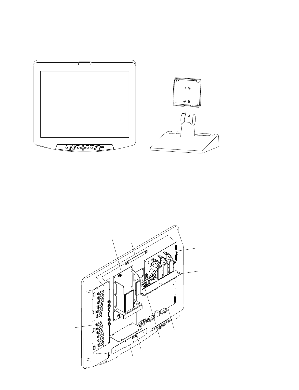
1-1. Appearance Figure
Section 1
Service Overview
LMD-2140MD
1-2. Board Locations
SU-560
Switching regulator
X
G1
T
LMD-2140MD
D2
B
B2
Q
H
1-1
Page 6
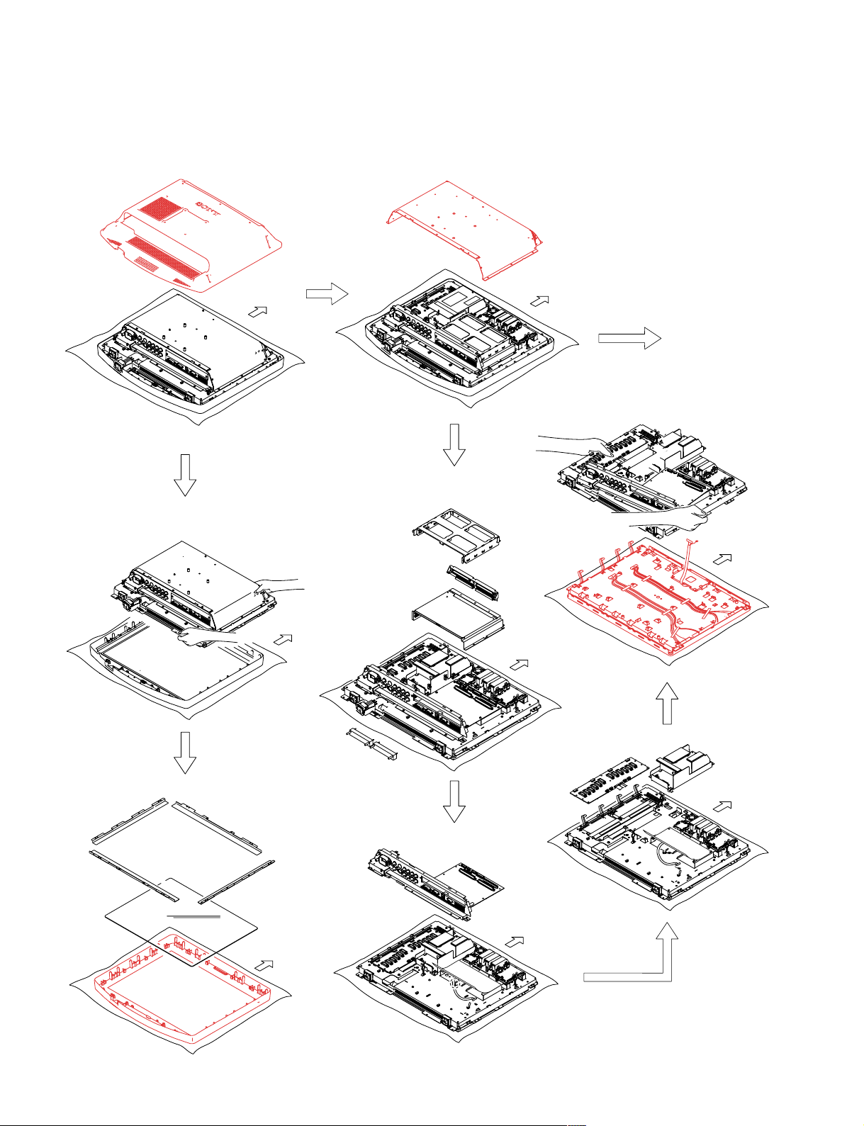
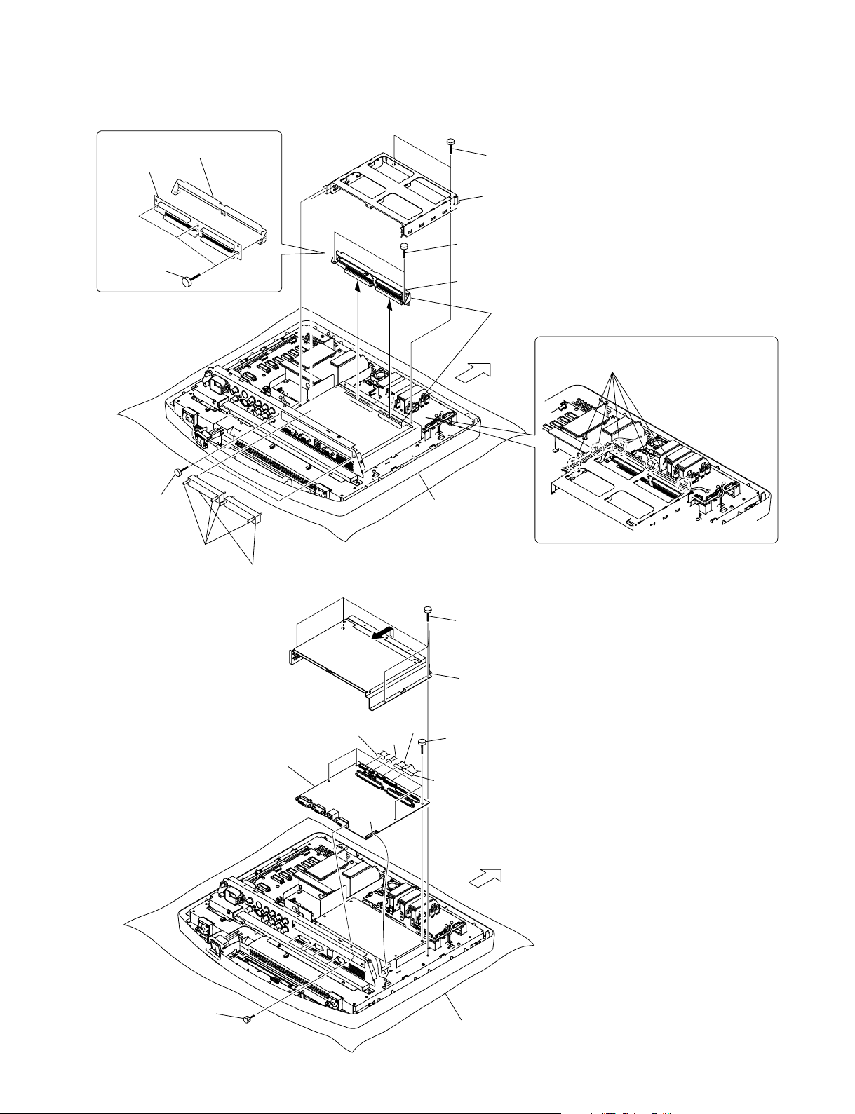
1-3. Disassembly
1-3-1. Rear Cabinet
1-3-3. Bezel Assembly
Upper
Side
1-3-2. Shield Case Assembly
Upper
Side
A
1-3-4. LCD Module-1
Upper
Side
Upper
Side
Upper
Side
!-
1-3-5. LCD Module-2
Upper
Side
Upper
Side
Upper
Side
1-2
LMD-2140MD
Page 7
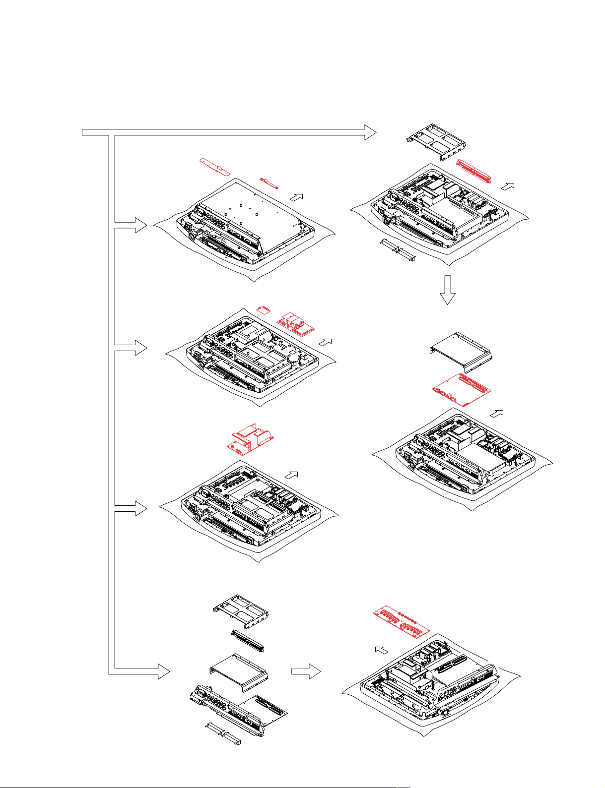
A
1-3-6. H Board and X Board
Upper
Side
1-3-7. G1 Board and B2 board
1-3-8. T Board
Upper
Side
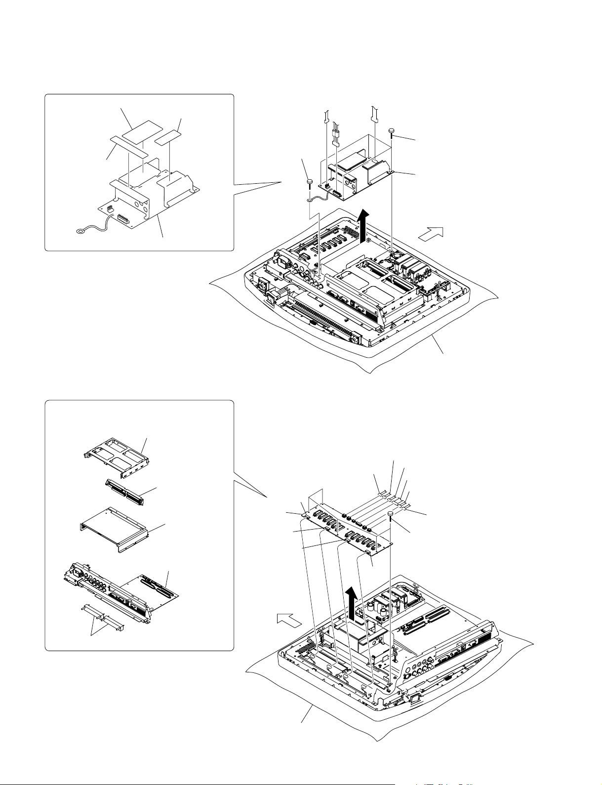
1-3-10. Switching Regulator
Upper
Side
For removal procedure,
refer to "LCD Module-1.-2".
Upper
Side
1-3-9. B Board
Upper
Side
1-3-11. D2 Board
LMD-2140MD
Upper
Side
1-3
Page 8
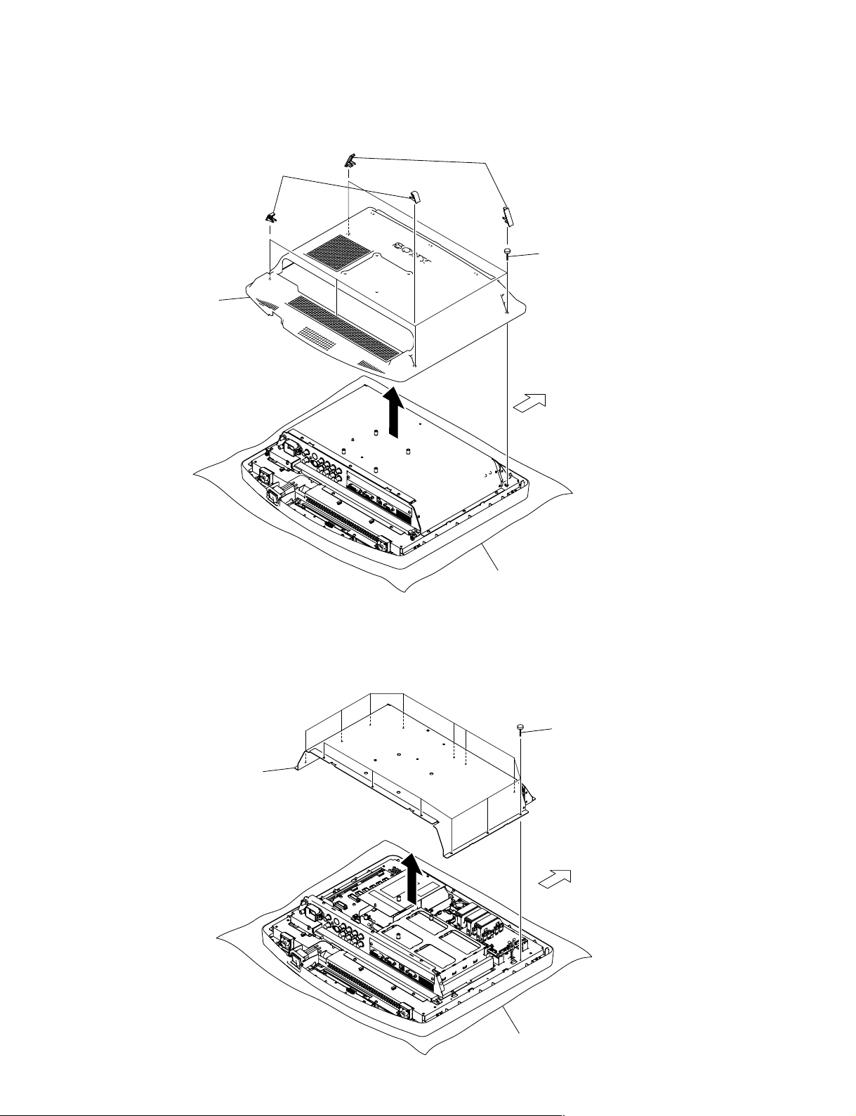
1-3-1. Rear Cabinet
4
Rear cabinet
2 Two s
A assemblies
crew cover
1 Two s
B assemblies
crew cover
3
Five screws
(+B 4 x10)
Upper
Side
1-3-2. Shield Case Assembly
2
Shield case assembly
Cushion
1
Thirteen screws
(+BVTT 3 x 6)
Upper
Side
1-4
Cushion
LMD-2140MD
Page 9
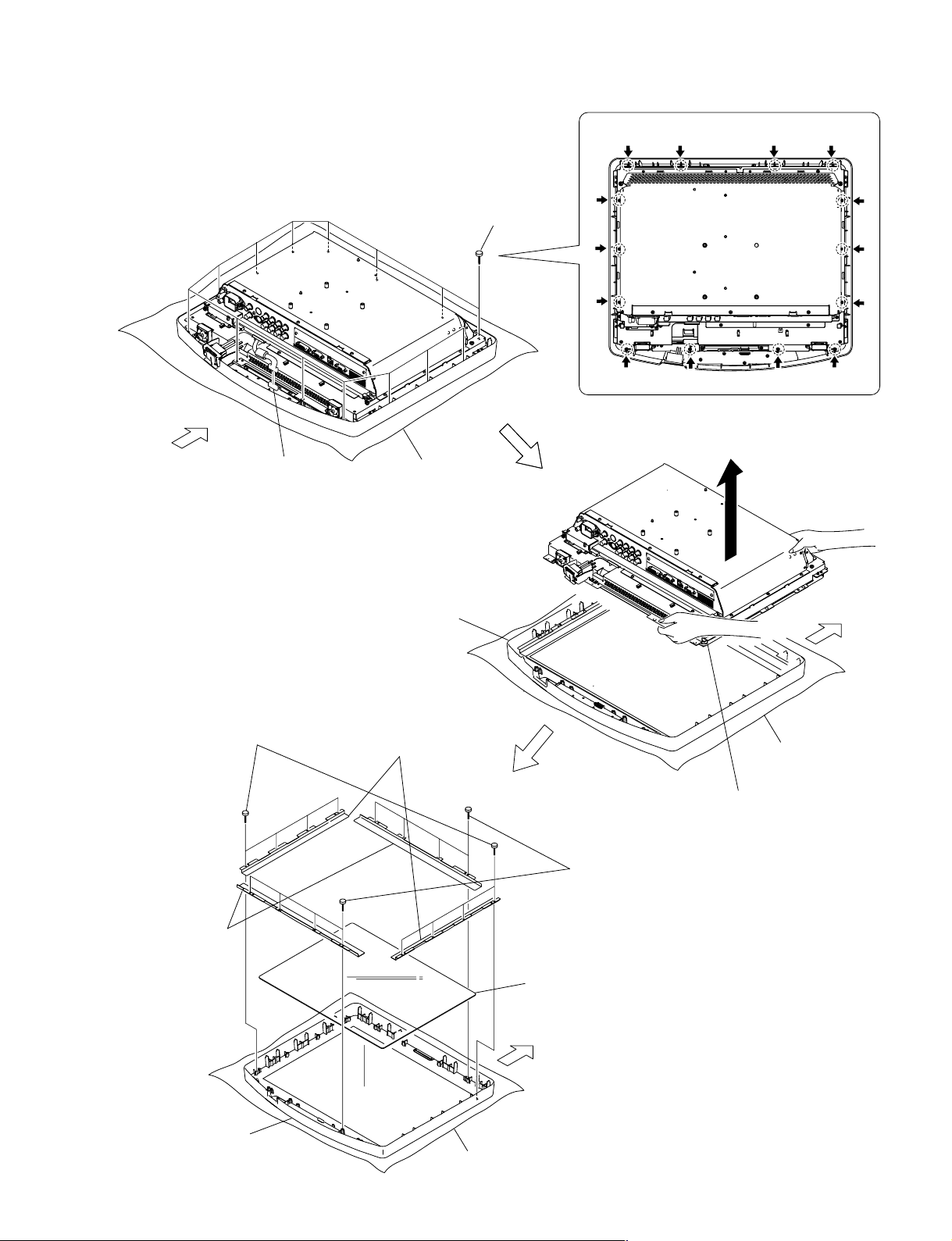
1-3-3. Bezel Assembly
2
Fourteen screws
(+BVTP 3 x10)
1
Connector
CN1001
3 LCD panel section,
Shield case assembly, etc.
4 Bezel section
5 Eight screws
(+BVTP 3 x 10)
6 Two bracket (A)
assemblies
8
Two bracket (B)
assemblies
7
Eight screws
(+BVTP 3 x 10)
0
Bezel assembly
9
Protection plate
Upper
Side
Upper
Side
Upper
Side
Cushion
Cushion
Cushion
LMD-2140MD
1-5
Page 10
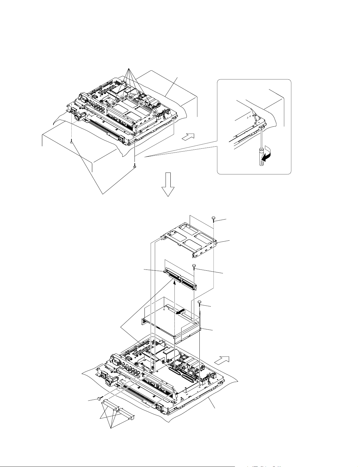
1-3-4. LCD Module-1
1
(+PSW 3 x 8)
Four screws
2
Four clamps
Cushion
Upper
Side
6
Two screws
(+BVTT 3 x 6)
9
5
Two screws
(+BVTT 3 x 6)
0 Bracket (T),
T board
Board to board
CN803
CN4100
CN804
CN4101
7
Option case assembly
8
Two screws
(+BVTT 3 x 6)
!- Five screws
(+BVTT 3 x 6)
!= Remove the case in the
direction of the arrow.
Upper
Side
1-6
Cushion
4 Two blank panel
assemblies
3 Loosen four screws
LMD-2140MD
Page 11
1-3-5. LCD Module-2
2
Six screws
(+BVTT 3 x 6)
Cushion
7 Two clamp
s
3
Screw
(+PSW 4 x 8)
1
Four screws
(+BVTT 3 x 6)
4
B board, Connector panel section
CN7501
6
Flip the shield sheet.
Upper
Side
5
Screw
(+BVTT 3 x 6)
!=
CN8202
D2 board
!- Five screws
(+BVTT 3 x 6)
CN8204
CN8203
0
Switching regulator, Sheet G,
Three radiation sheets
8
(+BVTT 3 x 6)
9
Screw
(+PSW 4 x 8)
CN8205
CN8209
CN8208
CN8207
CN8206
Four screws
!;
Connector panel section
,
Frame, G1 board, etc.
!\ Connector
!' LCD module
Upper
Side
![
Five screws
(+BVTT 3 x 6)
Upper
Side
Cushion
Upper
Side
LMD-2140MD
Cushion
!]
Four screws
(+PSW 3 x 8)
Cushion
1-7
Page 12
1-3-6. H Board and X Board
1
Four screws
(+BVTP 3 x 10)
2
H board
CN1001
CN1901
3
Two screws
(+BVTT 3 x 6)
4
X board
Upper
Side
1-3-7. G1 Board and B2 Board
4
Radiation sheet (C)
5
G1 board
6
Three screws
(+BVTT 3 x 6)
7 B board
CN1301
CN1302
CN601
CN606
Cushion
CN607
1
Four screws
(+BVTT 3 x 6)
3
G1 board,
Radiation sheet (C)
Upper
Side
CN602
CN603
CN605
CN604
1-8
2 Three
Cushion
clamps
LMD-2140MD
Page 13
1-3-8. T Board
Bracket (T)
!-
!=
T board
0
Three screws
(+PSW 3 x 6)
3
Two screws
(+BVTT 3 x 6)
CN803
CN4100
CN4101
CN804
Cushion
5
Two screws
(+BVTT 3 x 6)
6
Option case assembly
7
Two screws
(+BVTT 3 x 6)
9 T board,
Bracket (T)
8
Board to board
Upper
Side
4
Five clamps
1 Loosen four screws
1-3-9. B Board
2 Two blank panel
assemblies
5 B board
CN2702
CN7501
CN301
CN3
1
Five screws
(+BVTT 3 x 6)
2
Remove the case in the
direction of the arrow.
4
Four screws
(+BVTT 3 x 6)
CN501
Upper
Side
3Six hexagon
LMD-2140MD
screws
Cushion
1-9
Page 14
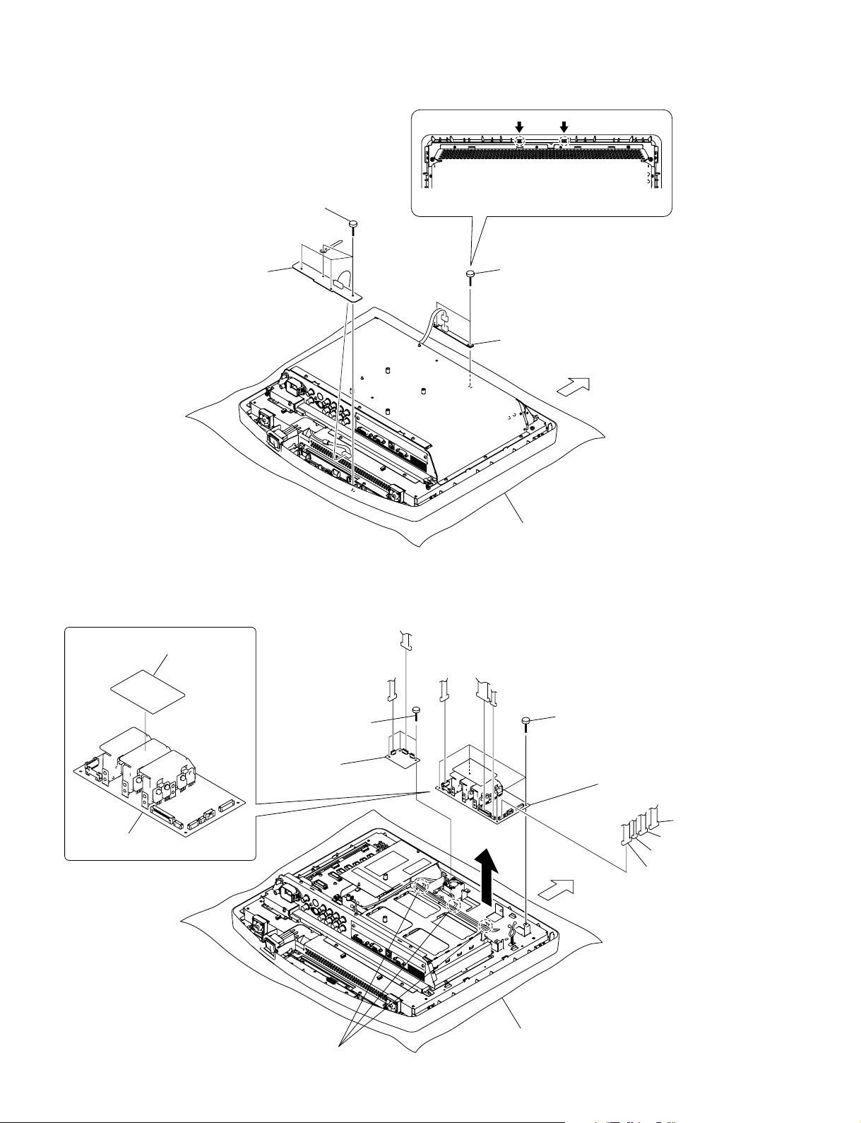
1-3-10. Switching Regulator
5
Radiation sheet (C)
6
Radiation sheet (D)
1-3-11. D2 Board
4
Radiation sheet (B)
7
Switching regulator
2
Screw
(+PSW 4 x 8)
CN1
CN2
CN103
1
Four screws
(+BVTT 3 x 6)
3
Switching regulator,
Three radiation sheets (B,C,D)
Upper
Side
Cushion
For removal procedure, refer to "LCD Panel-1.-2".
2
Option case assembly
3 Bracket (T),
5
B board, Connector panel section
1 Two blank panel assemblies
T board
4 Case B
7 D2
CN8205
board
CN8204
CN8203
Upper
Side
CN8208
CN8209
CN8202
CN8210
CN8201
CN8207
CN8206
6
Five screws
(+BVTT 3 x 6)
1-10
Cushion
LMD-2140MD
Page 15
1-4. Warning on Power Connection
Use a proper power cord for your local power supply
Plug type
Female end
Cord type
Rated Voltage & Current
Safety approval
The United States
HOSPITAL GRADE
E41395
E41395-A
10A/125V
UL
Canada
HOSPITAL GRADE
LL33182
LL76662
10A/125V
CSA
Continental Europe
LP-34A
LS-60
H05VV-F
10A/250V
VDE
LMD-2140MD
1-11
Page 16

Page 17

Section 2
Electrical Adjustments
2-1. Preparation
. Required tools and measuring equipment
Luminance meter :Minolta CA-210, CA-110 or equiva-
lent.
If Minolta CA-210, CA-110 or
equivalent, is not available, make
adjustment by comparing the LCD
monitor with the reference monitor
that has already been calibrated
correctly.
Signal generator : VG-854 or equivalent
. Warm-up time
Before starting adjustment, allow a warm-up of minimum
120 minutes to stabilize the back light of the LCD panel.
. How to enter service mode
1. Press MENU to display the MENU screen.
2. Press the APA and ENTER buttons simultaneously
with MENU screen appeared.
. HIGH adjustment
1. Select HIGH from COLOR TEMP and set it by
pressing ENTER.
Target value : x = 0.283, y = 0.298
2. Select ADJUST GAIN, and adjust the GAIN. Adjust
using R and B while G is fixed.
3. Select ADJUST BIAS, and adjust the BIAS. Adjust
using R and B while G is fixed.
4. Repeat steps 2 and 3 until all of the required specifications are met all at the same time.
. LOW adjustment
1. Select LOW from COLOR TEMP and set it by
pressing ENTER.
Target value : x = 0.313, y = 0.329
2. Select ADJUST GAIN, and adjust the GAIN.
Adjust using R and B while G is fixed.
3. Select ADJUST BIAS, and adjust the BIAS.
Adjust using R and B while G is fixed.
4. Repeat steps 2 and 3 until all of the required specifications are met all at the same time.
Preparing the power supply and signals
1. Connect the supplied power cord to AC IN of the set.
Power voltage : 100 to 240 V AC, 50/60Hz
2. Connect the signal coming from the VG-854 to the
VIDEO IN connector of the set. Because this signal is
used for synchronization, any type of signal can be
used as long as the signal has the receivable format.
3. Turn on the power of the LMD-2140MD. For set,
select the signal that is used for signal input.
2-2. White Balance Adjustment
1. Move the cursor to SIG using the Down ↓ key and
press ENTER to enter the SIGNAL layer.
2. Move the cursor to WHITE BALANCE using the
Down ↓ key and press ENTER to enter the SIGNAL/
WHITE BALANCE layer.
To move the cursor to select an item, use the Up ↑ or
Down ↓ key. To set the selected item, press the ENTER
key.
. LOW2 adjustment
1. Select LOW2 from COLOR TEMP and set it by
pressing ENTER.
Target value : x = 0.330, y = 0.345
2. Select ADJUST GAIN, and adjust the GAIN.
Adjust using R and B while G is fixed.
3. Select ADJUST BIAS, and adjust the BIAS.
Adjust using R and B while G is fixed.
4. Repeat steps 2 and 3 until all of the required specifications are met all at the same time.
. LOW3 adjustment
1. Select LOW3 from COLOR TEMP and set it by
pressing ENTER.
Target value : x = 0.316, y = 0.326
2. Select ADJUST GAIN, and adjust the GAIN.
Adjust using R and B while G is fixed.
3. Select ADJUST BIAS, and adjust the BIAS.
Adjust using R and B while G is fixed.
4. Repeat steps 2 and 3 until all of the required specifications are met all at the same time.
LMD-2140MD
2-1
Page 18

2-3. A/D Adjustment (COMPONENT)
2-4. A/D Adjustment (RGB)
1. Input the 575/50I 100% 8 color bar COMPONENT
signal to the LMD-2140MD.
2. Press the COMPONENT switch to accept the COMPONENT input signal.
3. Enter the Service menu, then select SIG → SIGNAL
LEVEL → AUTO ADJ. Perform the following
automatic adjustments.
. Y LEVEL
. PB LEVEL
. PR LEVEL
. Y OFFSET
. PB OFFSET
. PR OFFSET
4. Confirm that the A/D AUTO ADJ has terminated
normally and the monitor screen is normally displayed.
5. Perform the adjustments of items 1-2 to 1-4 in table 1
shown below by repeating the above described
procedures.
However, before performing AUTO ADJ, adjust the
COMPONENT level or NTSC SETUP appropriately
according to the respective conditions described in
table 1.
COMPONENT selection input
1-1 575/50I 100% 8 color bar signal
Y/G LEVEL
PB/B LEVEL Conditions :
PR/R LEVEL
Y/G OFFSET NTSC SETUP No specific conditions
PB/B OFFSET
PR/R OFFSET
1-2 480/60I BETA0 100% 8 color bar signal
Y/G LEVEL
PB/B LEVEL Conditions :
PR/R LEVEL COMPONENT LEVEL BETA 0
Y/G OFFSET NTSC SETUP No specific conditions
PB/B OFFSET
PR/R OFFSET
1-3 480/60I BETA7.5 100% 8 color bar signal
Y/G LEVEL
PB/B LEVEL Conditions :
PR/R LEVEL COMPONENT LEVEL BETA 7.5
Y/G OFFSET NTSC SETUP No specific conditions
PB/B OFFSET
PR/R OFFSET
1-4 1080/60I 100% 8 color bar signal
Y/G LEVEL
PB/B LEVEL Conditions :
PR/R LEVEL
Y/G OFFSET NTSC SETUP No specific conditions
PB/B OFFSET
PR/R OFFSET
COMPONENT LEVEL No specific conditions
COMPONENT LEVEL No specific conditions
Table 1
2-2
1. Input the 480/60I 100% 8 color bar RGB signal to the
LMD-2140MD.
2. Press the RGB switch to accept the RGB input signal.
3. Enter the Service menu, then select SIG → SIGNAL
LEVEL → AUTO ADJ. Perform the following
automatic adjustments.
. Y LEVEL
. PB LEVEL
. PR LEVEL
. Y OFFSET
. PB OFFSET
. PR OFFSET
4. Confirm that the A/D AUTO ADJ has terminated
normally and the monitor screen is normally displayed.
5. Perform the adjustment of item 1-6 in table 2 shown
below by repeating the above described procedures.
RGB selection input
1-5 480/60I RGB 100% 8 color bar signal
Y /G LEVEL
PB/B LEVEL
PR/R LEVEL Conditions :
Y/G OFFSET No specific conditions
PB/B OFFSET
PR/R OFFSET
1-6 1080/60I RGB 100% 8 color bar signal
Y /G LEVEL
PB/B LEVEL
PR/R LEVEL Conditions :
Y/G OFFSET No specific conditions
PB/B OFFSET
PR/R OFFSET
Table 2
LMD-2140MD
Page 19
2-5. A/D Adjustment (COMPOSITE)
2-6. A/D Adjustment (Y/C)
1. Input the NTSC 100% 8 color bar COMPOSITE signal
to the LMD-2140MD.
2. Press the COMPOSITE switch to accept the COMPOSITE input signal.
3. Enter the Service menu, then select SIG → SIGNAL
LEVEL → AUTO ADJ. Perform the following
automatic adjustments.
. Y LEVEL
. PB LEVEL
. PR LEVEL
4. Confirm that the A/D AUTO ADJ has terminated
normally and the monitor screen is normally displayed.
5. Perform the adjustments of items 1-8 and 1-9 in table 3
shown below by repeating the above described
procedures.
COMPOSITE selection input
1-7 NTSC SETUP 0 100% 8 color bar signal
Y /G LEVEL
PB/B LEVEL Conditions :
PR/R LEVEL NTSC SETUP NTSC SETUP 0
1-8 PAL 100% 8 color bar signal
Y /G LEVEL
PB/B LEVEL Conditions :
PR/R LEVEL No specific conditions
1-9 NTSC SETUP 7.5 100% 8 color bar signal
Y /G LEVEL
PB/B LEVEL Conditions :
PR/R LEVEL NTSC SETUP NTSC SETUP 7.5
Table 3
1. Input the NTSC 100% 8 color bar Y/C signal to the
LMD-2140MD.
2. Press the Y/C switch to accept the Y/C input signal.
3. Enter the Service menu, then select SIG → SIGNAL
LEVEL → AUTO ADJ. Perform the following
automatic adjustments.
. Y LEVEL
. PB LEVEL
. PR LEVEL
4. Confirm that the A/D AUTO ADJ has terminated
normally and the monitor screen is normally displayed.
5. Perform the adjustments of items 1-11 and 1-12 in
table 4 shown below by repeating the above described
procedures.
Y/C selection input
1-10 NTSC SETUP 0 100% 8 color bar signal
Y /G LEVEL
PB/B LEVEL Conditions :
PR/R LEVEL NTSC SETUP NTSC SETUP 0
1-11 PAL 100% 8 color bar signal
Y /G LEVEL
PB/B LEVEL Conditions :
PR/R LEVEL No specific conditions
1-12 NTSC SETUP 7.5 100% 8 color bar signal
Y /G LEVEL
PB/B LEVEL Conditions :
PR/R LEVEL NTSC SETUP NTSC SETUP 7.5
Table 4
LMD-2140MD
2-3
Page 20

2-7. A/D Adjustment (COMPUTER)
1. Input the 640 x 480 60 Hz 100% 8 color bar signal to
the LMD-2140MD.
2. Press the COMPUTER switch to accept the COMPUTER input signal.
3. Enter the Service menu, then select SIG → SIGNAL
LEVEL → AUTO ADJ. Perform the following
automatic adjustments.
. Y LEVEL
. PB LEVEL
. PR LEVEL
. Y OFFSET
. PB OFFSET
. PR OFFSET
4. Confirm that the A/D AUTO ADJ has terminated
normally and the monitor screen is normally displayed.
COMPUTER selection input
1-13 VGA60 100% 8 color bar signal
Y /G LEVEL
PB/B LEVEL
PR/R LEVEL Conditions :
Y/G OFFSET No specific conditions
PB/B OFFSET
PR/R OFFSET
Table 5
2-4
LMD-2140MD
Page 21
Section 3
1
TOP VIEW
1
2
3
4
5
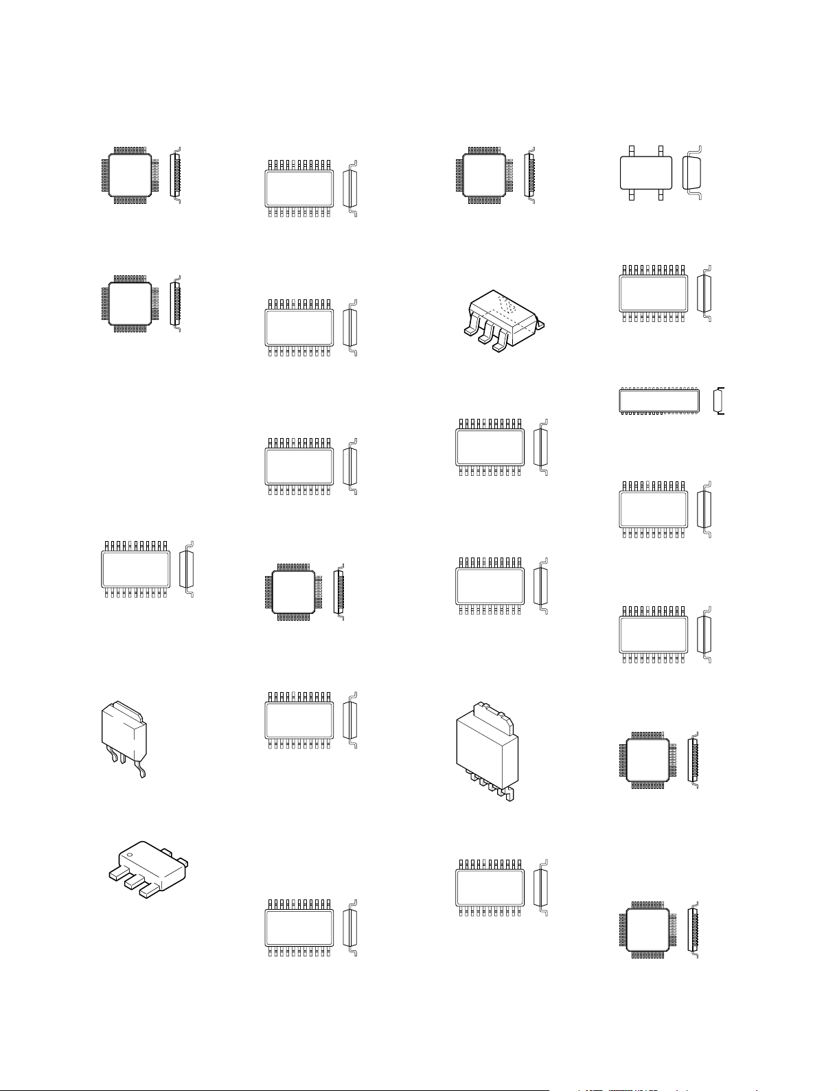
Semiconductors
IC
AD9882KSTZ-140
1
TOP VIEW
100pin QFP
AD9883AKST-110
1
TOP VIEW
80pin QFP
BA033FP
BA033FP-E2
BA10358FV-E2
FDS6690A
L5972D
L5972D013TR
NJM2903M
NJM2903M-TE2
TC7W53FU(TE12R)
TC7W53FU-TE12R
UPA1716G-E2
BD9766FV-E2
MB90098APF-G-168-ERE1
1
TOP VIEW
28pin SOP
BU9882F-WE2
TC74VHCT14AFT(EL)
1
TOP VIEW
14pin SOP
EMC6D102-CZC-TR
ICS1523MLFT-ER
1
TOP VIEW
24pin SOP
HD6417709SF133BV
IP00C713
256pin QFP
LP2985IM5X-3.3
PST9229NL
5
4
1
2
3
MBM29DL324BE-90PFTNLMD1100
1
TOP VIEW
48pin SOP
MSM56V16160F-8T3FM1
MSM56V16160F-8T4FM1
TC7W125FU-TE12R
1
8pin CHIP
THC63LVDM83R-T
1
TOP VIEW
56pin SOP
TL431CPK-E2
1
TOP VIEW
8pin DIP
TPS5103IDBR
1
TOP VIEW
20pin SOP
1
TOP VIEW
8pin SOP
BA18BC0FP-E2
BA25BC0FP-E2
BA25BC0FP-TE2
2
1
3
BD4831FVE-TR
BD4845FVE-TR
5
1
2
3
TPS5120DBTR
1
1
TOP VIEW
208pin QFP
HY57V641620HGTP-H
TOP VIEW
50pin SOP
PQ070XZ01ZPH
PQ1CZ41H2ZPH
1
TOP VIEW
30pin SOP
UPD64011AGM-8ED-A
1
TOP VIEW
54pin SOP
1
ICS1523M-ER
MAX202CSE
TOP VIEW
160pin QFP
MAX202CSE-T
TC74HC4053AFT(EL)
4
TC74LCX138FT(EL)
TC74VHC165FT (EL)
TC74VHC165FT(EL)
1
TOP VIEW
16pin SOP
TC7SZ125FU(TE85R)
1
TOP VIEW
5pin SOP
XC18V02-MEU1VP1-V100
XC18V02-MEU1VP1-V101
XC18V02-MEU1VS1-V101
XC9536XL-5-MEU1-V023
1
TOP VIEW
44pin QFP
LMD-2140MD
3-1
Page 22
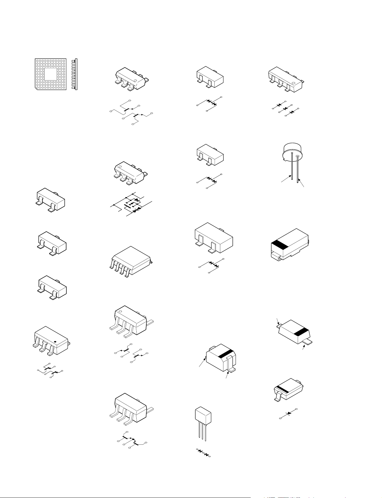
IC, Transistor, Diode
XC2S200E-6FTG256C
A
1
BOTTOM VIEW
256pin PGA
2SA1576A-T106-QR
2SA1610-T1Y34
2SA1610-Y33
2SC4081-R
2SC4081T106R
2SC4176-B34
2SC4176T1B33B34B35
DTC144EKA (T146)
DTC144EKA-T146
DTC144EUA-T106
MMBT3904
MMBT3904LT1
C
B
E
2SK3018-T106
D
G
S
DTA144EUA-T106
OUT
IN
GND
IMT2AT108
4
5
6
3
2
1
4
5
3
2
6
1
IMX2
IMX2-T109
4
3
2
1
4
3
2
1
RTQ035P02
RTQ035P02TR
6
1
2
3
1
2
3
SI4425DY-T1
D
S
S
S
G
UMH2NL02TN
1
2
3
6
1
2
3
UMW1NTR
1SS184
MA152WK-TX
5
6
2
5
6
2
3
1
3
1
1SS226
1SS226-TE85L
3
5
4
6
5
4
2
1
3
2
1
1SS302
1SS302-TE85L
HN1D03FU-TE85L
HN1D03FU-TE85R
4
5
6
3
2
1
4
5
3
2
6
1
MA3J14700LSO
CATHODE
ANODE
PTZ-TE25-27A
RB060L-40TE25
RB063L-30TE25
3
D
D
D
1
2
3
1
2
CATHODE
ANODE
RB160M-30TR
1SS352
1SS352-TPH3
1SS355TE-17
6
5
4
1SS357(T3SONY1)
MA111-TX
RD13SB-T1
UDZSTE-1713B
UDZSTE-173.9B
UDZS-TE17-5.1B
UDZSTE-175.1B
ANODE
RD3.3SB
RD3.3SB-T1
5
4
ANODE
CATHODE
RD12SB-T1
CATHODE
2
3-2
5
4
1
2
3
5
1
2
3
4
C10T03QL-11A
3
2
1
3
2
1
1
1
CATHODE
ANODE
2
LMD-2140MD
Page 23
SML-020MLTT87
SML-020MLTT87
4
3
1
3
4
1
UDZS-TE17-5.6B
ANODE
CATHODE
Diode
2
2
UDZSTE-175.6B
CATHODE
SML-011EBTT86
ã^ñ‚
ANODE
LMD-2140MD
3-3
Page 24

Page 25

4-1. Notes on Repair Parts
1. Safety Related Components Warning
w
Components marked ! are critical to safe operation.
Therefore, specified parts should be used in the case of
replacement.
2. Standardization of Parts
Some repair parts supplied by Sony differ from those
used for the unit. These are because of parts commonality and improvement.
Parts List has the present standardized repair parts.
3. Stock of Parts
Parts marked with “o” at SP (Supply Code) column of
the Spare Parts list may not be stocked. Therefore, the
delivery date will be delayed.
Items with no part number and no description are not
stocked because they are seldom required for routine
service.
Section 4
Spare Parts
4. Units for Capacitors, Inductors and Resistors
The following units are assumed in Schematic Diagrams, Electrical Parts List and Exploded Views
unless otherwise specified.
Capacitors : µF
Inductors : µH
Resistors : Ω
LMD-2140MD
4-1
Page 26
Cover
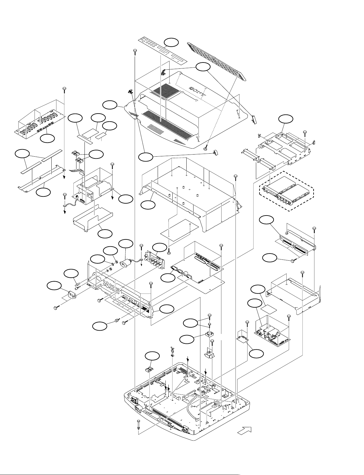
4-2. Exploded Views
27
28
5
+BVTT 3x6
C
+PSW 4x8
18
17
32
20
16
+BVTT 3x6
B
+B 4x10
11
22
14
8
+BVTT 3x6
+PWHTP 3x10
7
Option
+BVTT 3x6
BKM-227W,
BKM-229X
9
23
+PSW 3x12
D
24
26
+BVTT 3x6
31
19
25
13
+BVTT 3x6
+PSW 4x8
A
+BVTT 3x6
32
1
+BVTT 3x6
10
A
D
6
+BVTT 3x6
+BVTT 3x6
30
+BVTT 3x6
3
17
4
+BVTT 3x6
+BVTT 3x6
29
12
C
+BVTT 3x6
2
B
4-2
Upper
Side
LMD-2140MD
Page 27

No. Part No. SP Description
1 A-1088-792-A s MOUNTED CIRCUIT BOARD, Q
2 A-1088-794-A s MOUNTED CIRCUIT BOARD, B2
3 A-1088-800-A s MOUNTED CIRCUIT BOARD, B
4 A-1088-801-A s MOUNTED CIRCUIT BOARD, G1
5 A-1071-809-A s MOUNTED CIRCUIT BOARD, D2
6 A-1410-194-A s MOUNTED CIRCUIT BOARD, T
7 X-2025-299-1 s COVER ASSY(A), SCREW
8 X-2025-300-1 s ASSY, OPTION CASE
9 X-2025-301-2 s ASSY, SHIELD CASE
10 X-2025-356-3 s ASSY,CN PANEL
11 ! 1-468-893-11 s REGULATOR,SWITCHING
12 ! 1-787-034-11 s D.C. FAN
13 ! 1-819-054-11 s AC INLET
14 2-546-511-01 s COVER,SCREW(B)
16 ! 2-546-517-01 s SHEET,RADIATION(B)
17 ! 2-546-518-01 s SHEET,RADIATION(C)
18 ! 2-546-519-01 s SHEET,RADIATION(D)
19 ! 2-546-520-01 s SHEET G
20 ! 2-546-534-01 s CABINET, REAR
22 2-547-102-01 s LABEL, CONNECTOR
23 2-990-241-02 s HOLDER (A), PLUG
24 3-175-740-01 o TERMINAL
25 3-175-741-01 o NUT
26 3-175-742-01 o WASHER
27 4-095-186-01 o SHEET (D), RADIATION
Cover
28 4-095-194-01 o HEAT SINK (D)
29 4-382-854-21 s SCREW +PSW M3X14(EP-FE/ZN/CM2)
30 4-382-854-51 s SCREW +PSW M3X6(EP-FE/ZN/CM2)
31 4-635-966-01 s SCREW (HEX)
32 1-469-969-11 s CLAMP, FERRITE
7-682-562-04 s SCREW +B 4X10
7-682-950-09 s SCREW +PSW 3X12(EP-FE/ZNBK/CM2)
7-682-961-01 s SCREW +PSW 4X8
7-685-871-01 s SCREW,+BVTT 3X6
7-685-903-31 s SCREW,+PWHTP 3X10(EP-FE/ZNBK/C)
LMD-2140MD
4-3
Page 28

Panel
101
103
109
111
102
106
104
110
110
105
Upper
Side
+BVTP 3x10
+BVTT 3x6
+BVTP 3x10
+BVTP 3x10
+BVTP 3x10
+BVTP 3x10
+BVTP 3x10
+BVTT 3x6
+PSW 3x8
+BVTT 3x6
105
+BVTT 3x6
+BVTT 3x6
108
107
+BVTT 3x6
+BVTT 3x6
+BVTT 3x6
A
A
No. Part No. SP Description
101 A-1088-791-A s MOUNTED CIRCUIT BOARD, H
102 A-1088-796-A s MOUNTED CIRCUIT BOARD, X
103 ! X-2025-292-1 s ASSY,BEZEL
104 ! 1-762-179-21 s SWITCH, AC POWER
105 ! 1-787-034-11 s D.C. FAN
106 ! 1-805-323-51 s LCD MODULE
107 2-176-190-01 s CUSHION, PANEL
108 2-176-190-11 s CUSHION, PANEL
109 2-546-523-01 s PLATE,PROTECTION
110 4-382-854-21 s SCREW +PSW M3X14(EP-FE/ZN/CM2)
111 4-662-796-01 o CLIP,COATING
7-682-948-01 s SCREW +PSW 3X8
7-685-647-79 s SCREW +BVTP3X10(EP-FE/ZNBK/CM2)
7-685-871-01 s SCREW,+BVTT 3X6
4-4
LMD-2140MD
Page 29
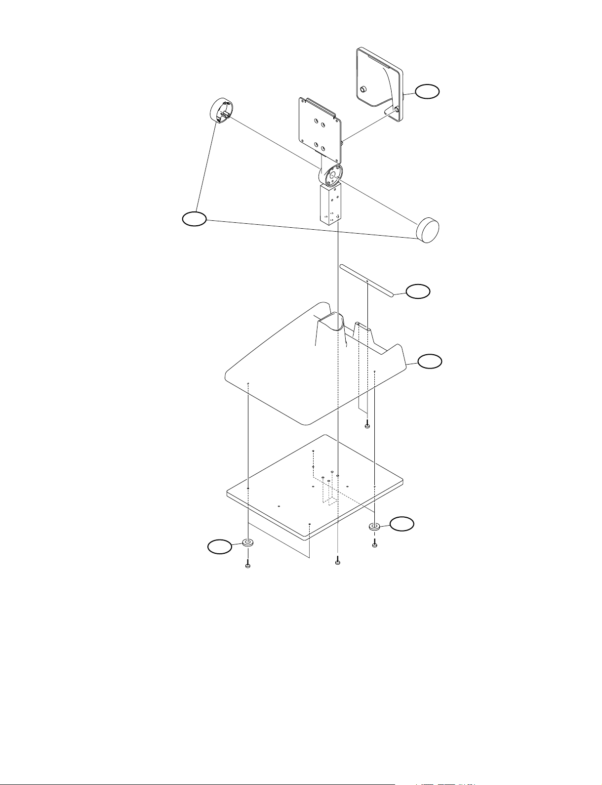
202
Display Stand (SU-560)
203
204
205
+B 3x10
No. Part No. SP Description
201 2-188-810-01 s COVER, BOTTOM
202 2-188-811-01 s COVER, HINGE
203 2-188-812-01 s COVER, VESA
204 2-541-782-01 s SHAFT. CABLE
205 4-310-333-01 s CUSHION, FOOT
201
+B 3x8
205
+BVTP 4x12
+B 4x10
7-685-647-71 s +B 3x10
7-685-661-14 s +BVTP 4x12(EP-FE/CU.NI.CR)
7-682-548-09 s SCREW +B 3x8
7-682-562-09 s +B 4x10 (EP-FE/ZNBK/CM2)
LMD-2140MD
4-5
Page 30

4-3. Electrical Parts List
CAUTION: DOUBLE POLE/NEUTRAL FUSING
------B BOARD
------ Ref. No.
or Q’ty Part No. SP Description
1pc A-1088-800-A s MOUNTED CIRCUIT BOARD, B
C1 1-162-970-11 s CAPACITOR CERAMIC 0.01MF/25V B
C2 1-107-826-11 s CAPACITOR,CHIP CERAMIC 0.1MF
C3 1-107-826-11 s CAPACITOR,CHIP CERAMIC 0.1MF
C4 1-107-826-11 s CAPACITOR,CHIP CERAMIC 0.1MF
C5 1-107-826-11 s CAPACITOR,CHIP CERAMIC 0.1MF
C6 1-107-826-11 s CAPACITOR,CHIP CERAMIC 0.1MF
C7 1-126-391-11 s CAPACITOR ELECT 47MF/6.3V(105)
C8 1-162-970-11 s CAPACITOR CERAMIC 0.01MF/25V B
C9 1-126-412-11 s CAPACITOR,ELECT 220MF/4V(CHIP)
C13 1-126-392-11 s CAPACITOR,CHIP ELECT100MF/6.3V
C14 1-125-837-91 s CAPACITOR,CHIP CERAMIC1MF/6.3V
C15 1-162-970-11 s CAPACITOR CERAMIC 0.01MF/25V B
C16 1-162-970-11 s CAPACITOR CERAMIC 0.01MF/25V B
C17 1-162-970-11 s CAPACITOR CERAMIC 0.01MF/25V B
C18 1-162-970-11 s CAPACITOR CERAMIC 0.01MF/25V B
C19 1-162-970-11 s CAPACITOR CERAMIC 0.01MF/25V B
C20 1-162-970-11 s CAPACITOR CERAMIC 0.01MF/25V B
C21 1-162-970-11 s CAPACITOR CERAMIC 0.01MF/25V B
C22 1-162-970-11 s CAPACITOR CERAMIC 0.01MF/25V B
C23 1-162-970-11 s CAPACITOR CERAMIC 0.01MF/25V B
C24 1-162-970-11 s CAPACITOR CERAMIC 0.01MF/25V B
C25 1-162-970-11 s CAPACITOR CERAMIC 0.01MF/25V B
C26 1-162-970-11 s CAPACITOR CERAMIC 0.01MF/25V B
C27 1-162-970-11 s CAPACITOR CERAMIC 0.01MF/25V B
C28 1-164-315-11 s CAPACITOR,CERAMIC 470PF/50V CH
C29 1-164-315-11 s CAPACITOR,CERAMIC 470PF/50V CH
C30 1-162-970-11 s CAPACITOR CERAMIC 0.01MF/25V B
C31 1-162-970-11 s CAPACITOR CERAMIC 0.01MF/25V B
C32 1-162-970-11 s CAPACITOR CERAMIC 0.01MF/25V B
C33 1-162-970-11 s CAPACITOR CERAMIC 0.01MF/25V B
C34 1-162-970-11 s CAPACITOR CERAMIC 0.01MF/25V B
C35 1-162-970-11 s CAPACITOR CERAMIC 0.01MF/25V B
C36 1-162-970-11 s CAPACITOR CERAMIC 0.01MF/25V B
C37 1-162-970-11 s CAPACITOR CERAMIC 0.01MF/25V B
C38 1-162-970-11 s CAPACITOR CERAMIC 0.01MF/25V B
C39 1-162-970-11 s CAPACITOR CERAMIC 0.01MF/25V B
C40 1-162-970-11 s CAPACITOR CERAMIC 0.01MF/25V B
C41 1-162-970-11 s CAPACITOR CERAMIC 0.01MF/25V B
C42 1-162-970-11 s CAPACITOR CERAMIC 0.01MF/25V B
C43 1-162-970-11 s CAPACITOR CERAMIC 0.01MF/25V B
C44 1-162-970-11 s CAPACITOR CERAMIC 0.01MF/25V B
C45 1-162-970-11 s CAPACITOR CERAMIC 0.01MF/25V B
C46 1-162-970-11 s CAPACITOR CERAMIC 0.01MF/25V B
C47 1-162-970-11 s CAPACITOR CERAMIC 0.01MF/25V B
C48 1-162-970-11 s CAPACITOR CERAMIC 0.01MF/25V B
C49 1-127-692-11 s CAP, CHIP CERAMIC 10MF B 3216
C50 1-127-692-11 s CAP, CHIP CERAMIC 10MF B 3216
C51 1-126-391-11 s CAPACITOR ELECT 47MF/6.3V(105)
C52 1-162-970-11 s CAPACITOR CERAMIC 0.01MF/25V B
C53 1-162-970-11 s CAPACITOR CERAMIC 0.01MF/25V B
C54 1-107-826-11 s CAPACITOR,CHIP CERAMIC 0.1MF
C55 1-131-998-11 s CAP, SOLID ELECT 82MF 6.3 V
C56 1-162-970-11 s CAPACITOR CERAMIC 0.01MF/25V B
C57 1-162-970-11 s CAPACITOR CERAMIC 0.01MF/25V B
C501 1-162-970-11 s CAPACITOR CERAMIC 0.01MF/25V B
(B BOARD)
Ref. No.
or Q’ty Part No. SP Description
C502 1-100-159-91 s CAP, CERAMIC 22MF B (SMD) 3216
C503 1-162-970-11 s CAPACITOR CERAMIC 0.01MF/25V B
C504 1-100-159-91 s CAP, CERAMIC 22MF B (SMD) 3216
C505 1-162-970-11 s CAPACITOR CERAMIC 0.01MF/25V B
C506 1-128-396-11 s CAPACITOR,ELECT 470MF/10V CHIP
C507 1-162-970-11 s CAPACITOR CERAMIC 0.01MF/25V B
C508 1-128-396-11 s CAPACITOR,ELECT 470MF/10V CHIP
C509 1-162-970-11 s CAPACITOR CERAMIC 0.01MF/25V B
C510 1-128-396-11 s CAPACITOR,ELECT 470MF/10V CHIP
C511 1-162-970-11 s CAPACITOR CERAMIC 0.01MF/25V B
C512 1-128-396-11 s CAPACITOR,ELECT 470MF/10V CHIP
C513 1-100-159-91 s CAP, CERAMIC 22MF B (SMD) 3216
C514 1-162-970-11 s CAPACITOR CERAMIC 0.01MF/25V B
C701 1-107-826-11 s CAPACITOR,CHIP CERAMIC 0.1MF
C702 1-107-826-11 s CAPACITOR,CHIP CERAMIC 0.1MF
C703 1-107-826-11 s CAPACITOR,CHIP CERAMIC 0.1MF
C704 1-127-692-11 s CAP, CHIP CERAMIC 10MF B 3216
C705 1-107-826-11 s CAPACITOR,CHIP CERAMIC 0.1MF
C706 1-162-967-11 s CAPACITOR,CERAMIC 3300PF/50V B
C707 1-164-217-11 s CAPACITOR,CERAMIC 150PF/50V CH
C708 1-127-692-11 s CAP, CHIP CERAMIC 10MF B 3216
C709 1-107-826-11 s CAPACITOR,CHIP CERAMIC 0.1MF
C710 1-107-826-11 s CAPACITOR,CHIP CERAMIC 0.1MF
C711 1-107-826-11 s CAPACITOR,CHIP CERAMIC 0.1MF
C712 1-127-692-11 s CAP, CHIP CERAMIC 10MF B 3216
C713 1-107-826-11 s CAPACITOR,CHIP CERAMIC 0.1MF
C714 1-127-692-11 s CAP, CHIP CERAMIC 10MF B 3216
C715 1-107-826-11 s CAPACITOR,CHIP CERAMIC 0.1MF
C2504 1-162-927-11 s CAPACITOR,CERAMIC 100PF/50V CH
C2505 1-162-927-11 s CAPACITOR,CERAMIC 100PF/50V CH
C2506 1-164-218-11 s CAPACITOR,CERAMIC 180PF/50V CH
C2507 1-164-218-11 s CAPACITOR,CERAMIC 180PF/50V CH
C2508 1-162-927-11 s CAPACITOR,CERAMIC 100PF/50V CH
C2509 1-162-927-11 s CAPACITOR,CERAMIC 100PF/50V CH
C2510 1-125-837-91 s CAPACITOR,CHIP CERAMIC1MF/6.3V
C2511 1-126-392-11 s CAPACITOR,CHIP ELECT100MF/6.3V
C2512 1-107-826-11 s CAPACITOR,CHIP CERAMIC 0.1MF
C2513 1-107-826-11 s CAPACITOR,CHIP CERAMIC 0.1MF
C2514 1-107-826-11 s CAPACITOR,CHIP CERAMIC 0.1MF
C2515 1-162-927-11 s CAPACITOR,CERAMIC 100PF/50V CH
C2516 1-162-927-11 s CAPACITOR,CERAMIC 100PF/50V CH
C2518 1-125-891-11 s CAPACITOR CERAMIC 0.47MF/10V
C2519 1-107-826-11 s CAPACITOR,CHIP CERAMIC 0.1MF
C2520 1-162-959-11 s CAPACITOR,CERAMIC 330PF/50V SL
C2521 1-107-826-11 s CAPACITOR,CHIP CERAMIC 0.1MF
C2524 1-135-344-11 s CAPACITOR,SOLID ELECT 270MF
C2525 1-162-970-11 s CAPACITOR CERAMIC 0.01MF/25V B
C2526 1-162-970-11 s CAPACITOR CERAMIC 0.01MF/25V B
C2527 1-165-875-11 s CAPACITOR, CHIP CERAMIC 10MF B
C2550 1-162-970-11 s CAPACITOR CERAMIC 0.01MF/25V B
C2551 1-137-894-21 s CAPACITOR,ELECT(CIHP TYPE) 470
C2552 1-162-970-11 s CAPACITOR CERAMIC 0.01MF/25V B
C2553 1-126-391-11 s CAPACITOR ELECT 47MF/6.3V(105)
C2554 1-162-966-11 s CAPACITOR,CERAMIC 2200PF/50V B
C2556 1-162-968-11 s CAPACITOR,CERAMIC 4700PF/50V B
C2557 1-162-966-11 s CAPACITOR,CERAMIC 2200PF/50V B
C2559 1-125-837-91 s CAPACITOR,CHIP CERAMIC1MF/6.3V
C2701 1-126-391-11 s CAPACITOR ELECT 47MF/6.3V(105)
C2702 1-162-970-11 s CAPACITOR CERAMIC 0.01MF/25V B
4-6
LMD-2140MD
Page 31

(B BOARD)
(B BOARD)
Ref. No.
or Q’ty Part No. SP Description
C2703 1-126-391-11 s CAPACITOR ELECT 47MF/6.3V(105)
C2704 1-162-970-11 s CAPACITOR CERAMIC 0.01MF/25V B
C2741 1-162-970-11 s CAPACITOR CERAMIC 0.01MF/25V B
C2742 1-162-970-11 s CAPACITOR CERAMIC 0.01MF/25V B
C2743 1-162-970-11 s CAPACITOR CERAMIC 0.01MF/25V B
C2761 1-162-970-11 s CAPACITOR CERAMIC 0.01MF/25V B
C2762 1-162-970-11 s CAPACITOR CERAMIC 0.01MF/25V B
C2763 1-162-970-11 s CAPACITOR CERAMIC 0.01MF/25V B
C2781 1-162-970-11 s CAPACITOR CERAMIC 0.01MF/25V B
C2782 1-162-970-11 s CAPACITOR CERAMIC 0.01MF/25V B
C2783 1-162-970-11 s CAPACITOR CERAMIC 0.01MF/25V B
C3101 1-107-826-11 s CAPACITOR,CHIP CERAMIC 0.1MF
C3102 1-107-826-11 s CAPACITOR,CHIP CERAMIC 0.1MF
C3103 1-127-760-11 s CAPACITOR,CERAMIC 4.7MF/6.3V
C3104 1-107-826-11 s CAPACITOR,CHIP CERAMIC 0.1MF
C3105 1-127-692-11 s CAP, CHIP CERAMIC 10MF B 3216
C3106 1-127-760-11 s CAPACITOR,CERAMIC 4.7MF/6.3V
C3107 1-107-826-11 s CAPACITOR,CHIP CERAMIC 0.1MF
C3108 1-107-826-11 s CAPACITOR,CHIP CERAMIC 0.1MF
C3109 1-162-970-11 s CAPACITOR CERAMIC 0.01MF/25V B
C3110 1-107-826-11 s CAPACITOR,CHIP CERAMIC 0.1MF
C3111 1-107-826-11 s CAPACITOR,CHIP CERAMIC 0.1MF
C3112 1-107-826-11 s CAPACITOR,CHIP CERAMIC 0.1MF
C3113 1-107-826-11 s CAPACITOR,CHIP CERAMIC 0.1MF
C3114 1-107-826-11 s CAPACITOR,CHIP CERAMIC 0.1MF
Ref. No.
or Q’ty Part No. SP Description
C3152 1-100-202-21 s CAP, CHIP ELECT 330MF
C3153 1-107-826-11 s CAPACITOR,CHIP CERAMIC 0.1MF
C3154 1-107-826-11 s CAPACITOR,CHIP CERAMIC 0.1MF
C3156 1-107-826-11 s CAPACITOR,CHIP CERAMIC 0.1MF
C3157 1-126-391-11 s CAPACITOR ELECT 47MF/6.3V(105)
C3158 1-107-826-11 s CAPACITOR,CHIP CERAMIC 0.1MF
C3159 1-162-970-11 s CAPACITOR CERAMIC 0.01MF/25V B
C3160 1-107-826-11 s CAPACITOR,CHIP CERAMIC 0.1MF
C3161 1-107-826-11 s CAPACITOR,CHIP CERAMIC 0.1MF
C3162 1-107-826-11 s CAPACITOR,CHIP CERAMIC 0.1MF
C3163 1-162-970-11 s CAPACITOR CERAMIC 0.01MF/25V B
C3164 1-107-826-11 s CAPACITOR,CHIP CERAMIC 0.1MF
C3165 1-165-176-11 s CAPACITOR,CERAMIC 47000PF/16V
C3166 1-162-927-11 s CAPACITOR,CERAMIC 100PF/50V CH
C3167 1-164-217-11 s CAPACITOR,CERAMIC 150PF/50V CH
C3168 1-107-826-11 s CAPACITOR,CHIP CERAMIC 0.1MF
C3169 1-107-826-11 s CAPACITOR,CHIP CERAMIC 0.1MF
C3170 1-107-826-11 s CAPACITOR,CHIP CERAMIC 0.1MF
C3171 1-162-915-11 s CAPACITOR,CERAMIC 10PF/50V CH
C3172 1-162-915-11 s CAPACITOR,CERAMIC 10PF/50V CH
C3173 1-107-826-11 s CAPACITOR,CHIP CERAMIC 0.1MF
C3174 1-126-391-11 s CAPACITOR ELECT 47MF/6.3V(105)
C3175 1-107-826-11 s CAPACITOR,CHIP CERAMIC 0.1MF
C3176 1-126-391-11 s CAPACITOR ELECT 47MF/6.3V(105)
C3177 1-107-826-11 s CAPACITOR,CHIP CERAMIC 0.1MF
C3115 1-107-826-11 s CAPACITOR,CHIP CERAMIC 0.1MF
C3116 1-127-760-11 s CAPACITOR,CERAMIC 4.7MF/6.3V
C3117 1-107-826-11 s CAPACITOR,CHIP CERAMIC 0.1MF
C3118 1-107-826-11 s CAPACITOR,CHIP CERAMIC 0.1MF
C3119 1-107-826-11 s CAPACITOR,CHIP CERAMIC 0.1MF
C3120 1-107-826-11 s CAPACITOR,CHIP CERAMIC 0.1MF
C3121 1-107-826-11 s CAPACITOR,CHIP CERAMIC 0.1MF
C3122 1-162-970-11 s CAPACITOR CERAMIC 0.01MF/25V B
C3123 1-107-826-11 s CAPACITOR,CHIP CERAMIC 0.1MF
C3124 1-107-826-11 s CAPACITOR,CHIP CERAMIC 0.1MF
C3125 1-107-826-11 s CAPACITOR,CHIP CERAMIC 0.1MF
C3126 1-127-760-11 s CAPACITOR,CERAMIC 4.7MF/6.3V
C3127 1-107-826-11 s CAPACITOR,CHIP CERAMIC 0.1MF
C3128 1-107-826-11 s CAPACITOR,CHIP CERAMIC 0.1MF
C3129 1-107-826-11 s CAPACITOR,CHIP CERAMIC 0.1MF
C3130 1-107-826-11 s CAPACITOR,CHIP CERAMIC 0.1MF
C3131 1-165-176-11 s CAPACITOR,CERAMIC 47000PF/16V
C3132 1-165-176-11 s CAPACITOR,CERAMIC 47000PF/16V
C3133 1-165-176-11 s CAPACITOR,CERAMIC 47000PF/16V
C3134 1-165-176-11 s CAPACITOR,CERAMIC 47000PF/16V
C3135 1-107-826-11 s CAPACITOR,CHIP CERAMIC 0.1MF
C3136 1-126-391-11 s CAPACITOR ELECT 47MF/6.3V(105)
C3140 1-107-826-11 s CAPACITOR,CHIP CERAMIC 0.1MF
C3141 1-162-970-11 s CAPACITOR CERAMIC 0.01MF/25V B
C3142 1-107-826-11 s CAPACITOR,CHIP CERAMIC 0.1MF
C3143 1-107-826-11 s CAPACITOR,CHIP CERAMIC 0.1MF
C3144 1-107-826-11 s CAPACITOR,CHIP CERAMIC 0.1MF
C3145 1-107-826-11 s CAPACITOR,CHIP CERAMIC 0.1MF
C3146 1-107-826-11 s CAPACITOR,CHIP CERAMIC 0.1MF
C3147 1-162-970-11 s CAPACITOR CERAMIC 0.01MF/25V B
C3178 1-126-391-11 s CAPACITOR ELECT 47MF/6.3V(105)
C3179 1-107-826-11 s CAPACITOR,CHIP CERAMIC 0.1MF
C3180 1-100-566-91 s CAP, CHIP CERAMIC 0.1MF B 1608
C3181 1-107-826-11 s CAPACITOR,CHIP CERAMIC 0.1MF
C3182 1-126-392-11 s CAPACITOR,CHIP ELECT100MF/6.3V
C3183 1-107-826-11 s CAPACITOR,CHIP CERAMIC 0.1MF
C3184 1-107-826-11 s CAPACITOR,CHIP CERAMIC 0.1MF
C3185 1-126-392-11 s CAPACITOR,CHIP ELECT100MF/6.3V
C3186 1-162-970-11 s CAPACITOR CERAMIC 0.01MF/25V B
C3189 1-107-826-11 s CAPACITOR,CHIP CERAMIC 0.1MF
C3190 1-107-826-11 s CAPACITOR,CHIP CERAMIC 0.1MF
C3191 1-126-391-11 s CAPACITOR ELECT 47MF/6.3V(105)
C3401 1-162-970-11 s CAPACITOR CERAMIC 0.01MF/25V B
C3402 1-162-970-11 s CAPACITOR CERAMIC 0.01MF/25V B
C3403 1-162-970-11 s CAPACITOR CERAMIC 0.01MF/25V B
C3404 1-162-970-11 s CAPACITOR CERAMIC 0.01MF/25V B
C3405 1-162-970-11 s CAPACITOR CERAMIC 0.01MF/25V B
C3406 1-162-970-11 s CAPACITOR CERAMIC 0.01MF/25V B
C3407 1-126-392-11 s CAPACITOR,CHIP ELECT100MF/6.3V
C3412 1-126-392-11 s CAPACITOR,CHIP ELECT100MF/6.3V
C3413 1-162-970-11 s CAPACITOR CERAMIC 0.01MF/25V B
C3414 1-162-970-11 s CAPACITOR CERAMIC 0.01MF/25V B
C3415 1-162-970-11 s CAPACITOR CERAMIC 0.01MF/25V B
C3416 1-162-970-11 s CAPACITOR CERAMIC 0.01MF/25V B
C3417 1-162-970-11 s CAPACITOR CERAMIC 0.01MF/25V B
C3418 1-162-970-11 s CAPACITOR CERAMIC 0.01MF/25V B
C3501 1-162-970-11 s CAPACITOR CERAMIC 0.01MF/25V B
C3502 1-162-970-11 s CAPACITOR CERAMIC 0.01MF/25V B
C3503 1-164-388-91 s CAPACITOR,CERAMIC 270PF/50V CH
C3504 1-162-921-11 s CAPACITOR,CERAMIC 33PF/50V CH
C3148 1-164-230-11 s CAPACITOR,CERAMIC 220PF/50V
C3149 1-162-959-11 s CAPACITOR,CERAMIC 330PF/50V SL
C3150 1-165-176-11 s CAPACITOR,CERAMIC 47000PF/16V
C3151 1-100-566-91 s CAP, CHIP CERAMIC 0.1MF B 1608
LMD-2140MD
C3505 1-162-970-11 s CAPACITOR CERAMIC 0.01MF/25V B
C3506 1-164-388-91 s CAPACITOR,CERAMIC 270PF/50V CH
C3507 1-162-921-11 s CAPACITOR,CERAMIC 33PF/50V CH
C3508 1-162-970-11 s CAPACITOR CERAMIC 0.01MF/25V B
4-7
Page 32

(B BOARD)
(B BOARD)
Ref. No.
or Q’ty Part No. SP Description
C3509 1-164-388-91 s CAPACITOR,CERAMIC 270PF/50V CH
C3510 1-162-921-11 s CAPACITOR,CERAMIC 33PF/50V CH
C3511 1-162-970-11 s CAPACITOR CERAMIC 0.01MF/25V B
C3512 1-115-340-11 s CAPACITOR CERAMIC 0.22MF/25V B
C3513 1-115-340-11 s CAPACITOR CERAMIC 0.22MF/25V B
C3514 1-115-340-11 s CAPACITOR CERAMIC 0.22MF/25V B
C3515 1-115-340-11 s CAPACITOR CERAMIC 0.22MF/25V B
C3516 1-115-340-11 s CAPACITOR CERAMIC 0.22MF/25V B
C3517 1-115-340-11 s CAPACITOR CERAMIC 0.22MF/25V B
C3518 1-107-826-11 s CAPACITOR,CHIP CERAMIC 0.1MF
C3519 1-162-970-11 s CAPACITOR CERAMIC 0.01MF/25V B
C3520 1-107-826-11 s CAPACITOR,CHIP CERAMIC 0.1MF
C3522 1-162-970-11 s CAPACITOR CERAMIC 0.01MF/25V B
C3523 1-107-826-11 s CAPACITOR,CHIP CERAMIC 0.1MF
C3524 1-107-826-11 s CAPACITOR,CHIP CERAMIC 0.1MF
C3526 1-107-826-11 s CAPACITOR,CHIP CERAMIC 0.1MF
C3527 1-162-970-11 s CAPACITOR CERAMIC 0.01MF/25V B
C3528 1-107-826-11 s CAPACITOR,CHIP CERAMIC 0.1MF
C3529 1-162-970-11 s CAPACITOR CERAMIC 0.01MF/25V B
C3530 1-107-826-11 s CAPACITOR,CHIP CERAMIC 0.1MF
C3531 1-131-998-11 s CAP, SOLID ELECT 82MF 6.3 V
C3532 1-107-826-11 s CAPACITOR,CHIP CERAMIC 0.1MF
C3533 1-162-970-11 s CAPACITOR CERAMIC 0.01MF/25V B
C3534 1-131-998-11 s CAP, SOLID ELECT 82MF 6.3 V
C3535 1-107-826-11 s CAPACITOR,CHIP CERAMIC 0.1MF
Ref. No.
or Q’ty Part No. SP Description
C3571 1-107-826-11 s CAPACITOR,CHIP CERAMIC 0.1MF
C3573 1-107-826-11 s CAPACITOR,CHIP CERAMIC 0.1MF
C3575 1-107-826-11 s CAPACITOR,CHIP CERAMIC 0.1MF
C3576 1-162-970-11 s CAPACITOR CERAMIC 0.01MF/25V B
C3577 1-107-826-11 s CAPACITOR,CHIP CERAMIC 0.1MF
C3578 1-162-970-11 s CAPACITOR CERAMIC 0.01MF/25V B
C3579 1-131-998-11 s CAP, SOLID ELECT 82MF 6.3 V
C3580 1-107-826-11 s CAPACITOR,CHIP CERAMIC 0.1MF
C3581 1-107-826-11 s CAPACITOR,CHIP CERAMIC 0.1MF
C3582 1-162-970-11 s CAPACITOR CERAMIC 0.01MF/25V B
C3583 1-107-826-11 s CAPACITOR,CHIP CERAMIC 0.1MF
C3584 1-165-176-11 s CAPACITOR,CERAMIC 47000PF/16V
C3585 1-162-968-11 s CAPACITOR,CERAMIC 4700PF/50V B
C3586 1-162-970-11 s CAPACITOR CERAMIC 0.01MF/25V B
C3587 1-162-928-11 s CAPACITOR,CERAMIC 120PF/50V CH
C3588 1-107-826-11 s CAPACITOR,CHIP CERAMIC 0.1MF
C3589 1-162-970-11 s CAPACITOR CERAMIC 0.01MF/25V B
C3590 1-107-826-11 s CAPACITOR,CHIP CERAMIC 0.1MF
C3591 1-162-970-11 s CAPACITOR CERAMIC 0.01MF/25V B
C3592 1-131-998-11 s CAP, SOLID ELECT 82MF 6.3 V
C3593 1-107-826-11 s CAPACITOR,CHIP CERAMIC 0.1MF
C3594 1-162-970-11 s CAPACITOR CERAMIC 0.01MF/25V B
C3595 1-162-970-11 s CAPACITOR CERAMIC 0.01MF/25V B
C3596 1-115-416-11 s CAPACITOR,CERAMIC 1000PF/25V
C3597 1-115-416-11 s CAPACITOR,CERAMIC 1000PF/25V
C3536 1-107-826-11 s CAPACITOR,CHIP CERAMIC 0.1MF
C3537 1-162-970-11 s CAPACITOR CERAMIC 0.01MF/25V B
C3538 1-107-826-11 s CAPACITOR,CHIP CERAMIC 0.1MF
C3539 1-165-176-11 s CAPACITOR,CERAMIC 47000PF/16V
C3540 1-162-968-11 s CAPACITOR,CERAMIC 4700PF/50V B
C3541 1-107-826-11 s CAPACITOR,CHIP CERAMIC 0.1MF
C3542 1-162-928-11 s CAPACITOR,CERAMIC 120PF/50V CH
C3543 1-107-826-11 s CAPACITOR,CHIP CERAMIC 0.1MF
C3544 1-162-970-11 s CAPACITOR CERAMIC 0.01MF/25V B
C3545 1-107-826-11 s CAPACITOR,CHIP CERAMIC 0.1MF
C3546 1-162-970-11 s CAPACITOR CERAMIC 0.01MF/25V B
C3547 1-131-998-11 s CAP, SOLID ELECT 82MF 6.3 V
C3548 1-107-826-11 s CAPACITOR,CHIP CERAMIC 0.1MF
C3549 1-162-970-11 s CAPACITOR CERAMIC 0.01MF/25V B
C3550 1-125-891-11 s CAPACITOR CERAMIC 0.47MF/10V
C3551 1-162-970-11 s CAPACITOR CERAMIC 0.01MF/25V B
C3552 1-125-891-11 s CAPACITOR CERAMIC 0.47MF/10V
C3553 1-162-970-11 s CAPACITOR CERAMIC 0.01MF/25V B
C3554 1-125-891-11 s CAPACITOR CERAMIC 0.47MF/10V
C3556 1-162-928-11 s CAPACITOR,CERAMIC 120PF/50V CH
C3557 1-164-677-11 s CAPACITOR,CERAMIC 0.033MF/16V
C3558 1-162-967-11 s CAPACITOR,CERAMIC 3300PF/50V B
C3559 1-165-176-11 s CAPACITOR,CERAMIC 47000PF/16V
C3560 1-164-677-11 s CAPACITOR,CERAMIC 0.033MF/16V
C3561 1-125-891-11 s CAPACITOR CERAMIC 0.47MF/10V
C3562 1-162-967-11 s CAPACITOR,CERAMIC 3300PF/50V B
C3563 1-107-826-11 s CAPACITOR,CHIP CERAMIC 0.1MF
C3564 1-107-826-11 s CAPACITOR,CHIP CERAMIC 0.1MF
C3565 1-131-998-11 s CAP, SOLID ELECT 82MF 6.3 V
C3566 1-107-826-11 s CAPACITOR,CHIP CERAMIC 0.1MF
C3598 1-115-416-11 s CAPACITOR,CERAMIC 1000PF/25V
C3599 1-115-416-11 s CAPACITOR,CERAMIC 1000PF/25V
C3600 1-115-416-11 s CAPACITOR,CERAMIC 1000PF/25V
C3601 1-115-416-11 s CAPACITOR,CERAMIC 1000PF/25V
C3602 1-115-416-11 s CAPACITOR,CERAMIC 1000PF/25V
C3603 1-100-159-91 s CAP, CERAMIC 22MF B (SMD) 3216
C3604 1-126-391-11 s CAPACITOR ELECT 47MF/6.3V(105)
C3605 1-107-826-11 s CAPACITOR,CHIP CERAMIC 0.1MF
C3606 1-126-391-11 s CAPACITOR ELECT 47MF/6.3V(105)
C3607 1-107-826-11 s CAPACITOR,CHIP CERAMIC 0.1MF
C3608 1-162-970-11 s CAPACITOR CERAMIC 0.01MF/25V B
C3610 1-162-970-11 s CAPACITOR CERAMIC 0.01MF/25V B
C3611 1-162-970-11 s CAPACITOR CERAMIC 0.01MF/25V B
C3612 1-107-826-11 s CAPACITOR,CHIP CERAMIC 0.1MF
C3613 1-162-970-11 s CAPACITOR CERAMIC 0.01MF/25V B
C3614 1-107-826-11 s CAPACITOR,CHIP CERAMIC 0.1MF
C3615 1-107-826-11 s CAPACITOR,CHIP CERAMIC 0.1MF
C3616 1-107-826-11 s CAPACITOR,CHIP CERAMIC 0.1MF
C3617 1-107-826-11 s CAPACITOR,CHIP CERAMIC 0.1MF
C3695 1-126-391-11 s CAPACITOR ELECT 47MF/6.3V(105)
C4002 1-107-826-11 s CAPACITOR,CHIP CERAMIC 0.1MF
C4003 1-107-826-11 s CAPACITOR,CHIP CERAMIC 0.1MF
C4004 1-126-392-11 s CAPACITOR,CHIP ELECT100MF/6.3V
C4006 1-126-392-11 s CAPACITOR,CHIP ELECT100MF/6.3V
C4007 1-126-392-11 s CAPACITOR,CHIP ELECT100MF/6.3V
C4008 1-107-826-11 s CAPACITOR,CHIP CERAMIC 0.1MF
C4009 1-107-826-11 s CAPACITOR,CHIP CERAMIC 0.1MF
C4010 1-162-970-11 s CAPACITOR CERAMIC 0.01MF/25V B
C4012 1-107-826-11 s CAPACITOR,CHIP CERAMIC 0.1MF
C4013 1-162-970-11 s CAPACITOR CERAMIC 0.01MF/25V B
C3567 1-162-970-11 s CAPACITOR CERAMIC 0.01MF/25V B
C3568 1-107-826-11 s CAPACITOR,CHIP CERAMIC 0.1MF
C3569 1-162-970-11 s CAPACITOR CERAMIC 0.01MF/25V B
C3570 1-107-826-11 s CAPACITOR,CHIP CERAMIC 0.1MF
C4014 1-107-826-11 s CAPACITOR,CHIP CERAMIC 0.1MF
C4015 1-107-826-11 s CAPACITOR,CHIP CERAMIC 0.1MF
C4016 1-126-392-11 s CAPACITOR,CHIP ELECT100MF/6.3V
C4017 1-126-392-11 s CAPACITOR,CHIP ELECT100MF/6.3V
4-8
LMD-2140MD
Page 33

(B BOARD)
(B BOARD)
Ref. No.
or Q’ty Part No. SP Description
C4018 1-107-826-11 s CAPACITOR,CHIP CERAMIC 0.1MF
C4019 1-107-826-11 s CAPACITOR,CHIP CERAMIC 0.1MF
C4020 1-107-826-11 s CAPACITOR,CHIP CERAMIC 0.1MF
C4021 1-125-837-91 s CAPACITOR,CHIP CERAMIC1MF/6.3V
C4022 1-107-826-11 s CAPACITOR,CHIP CERAMIC 0.1MF
C4023 1-125-837-91 s CAPACITOR,CHIP CERAMIC1MF/6.3V
C4024 1-162-970-11 s CAPACITOR CERAMIC 0.01MF/25V B
C4025 1-162-970-11 s CAPACITOR CERAMIC 0.01MF/25V B
C4026 1-162-970-11 s CAPACITOR CERAMIC 0.01MF/25V B
C4027 1-162-970-11 s CAPACITOR CERAMIC 0.01MF/25V B
C4028 1-162-970-11 s CAPACITOR CERAMIC 0.01MF/25V B
C4029 1-162-970-11 s CAPACITOR CERAMIC 0.01MF/25V B
C4030 1-126-412-11 s CAPACITOR,ELECT 220MF/4V(CHIP)
C4031 1-126-412-11 s CAPACITOR,ELECT 220MF/4V(CHIP)
C4032 1-107-826-11 s CAPACITOR,CHIP CERAMIC 0.1MF
C4033 1-107-826-11 s CAPACITOR,CHIP CERAMIC 0.1MF
C4034 1-162-970-11 s CAPACITOR CERAMIC 0.01MF/25V B
C4035 1-125-837-91 s CAPACITOR,CHIP CERAMIC1MF/6.3V
C4036 1-125-837-91 s CAPACITOR,CHIP CERAMIC1MF/6.3V
C4037 1-162-970-11 s CAPACITOR CERAMIC 0.01MF/25V B
C4038 1-162-970-11 s CAPACITOR CERAMIC 0.01MF/25V B
C4039 1-162-970-11 s CAPACITOR CERAMIC 0.01MF/25V B
C4040 1-107-826-11 s CAPACITOR,CHIP CERAMIC 0.1MF
C4041 1-107-826-11 s CAPACITOR,CHIP CERAMIC 0.1MF
C4042 1-107-826-11 s CAPACITOR,CHIP CERAMIC 0.1MF
Ref. No.
or Q’ty Part No. SP Description
C5031 1-107-826-11 s CAPACITOR,CHIP CERAMIC 0.1MF
C5032 1-107-826-11 s CAPACITOR,CHIP CERAMIC 0.1MF
C5033 1-107-826-11 s CAPACITOR,CHIP CERAMIC 0.1MF
C5034 1-107-826-11 s CAPACITOR,CHIP CERAMIC 0.1MF
C5035 1-107-826-11 s CAPACITOR,CHIP CERAMIC 0.1MF
C5036 1-107-826-11 s CAPACITOR,CHIP CERAMIC 0.1MF
C5501 1-126-392-11 s CAPACITOR,CHIP ELECT100MF/6.3V
C5502 1-107-826-11 s CAPACITOR,CHIP CERAMIC 0.1MF
C5503 1-107-826-11 s CAPACITOR,CHIP CERAMIC 0.1MF
C5504 1-107-826-11 s CAPACITOR,CHIP CERAMIC 0.1MF
C5505 1-107-826-11 s CAPACITOR,CHIP CERAMIC 0.1MF
C5506 1-107-826-11 s CAPACITOR,CHIP CERAMIC 0.1MF
C5507 1-107-826-11 s CAPACITOR,CHIP CERAMIC 0.1MF
C5508 1-107-826-11 s CAPACITOR,CHIP CERAMIC 0.1MF
C5509 1-107-826-11 s CAPACITOR,CHIP CERAMIC 0.1MF
C5510 1-107-826-11 s CAPACITOR,CHIP CERAMIC 0.1MF
C5511 1-162-970-11 s CAPACITOR CERAMIC 0.01MF/25V B
C5512 1-107-826-11 s CAPACITOR,CHIP CERAMIC 0.1MF
C5513 1-107-826-11 s CAPACITOR,CHIP CERAMIC 0.1MF
C5514 1-107-826-11 s CAPACITOR,CHIP CERAMIC 0.1MF
C5515 1-107-826-11 s CAPACITOR,CHIP CERAMIC 0.1MF
C5516 1-100-566-91 s CAP, CHIP CERAMIC 0.1MF B 1608
C5517 1-107-826-11 s CAPACITOR,CHIP CERAMIC 0.1MF
C5518 1-100-566-91 s CAP, CHIP CERAMIC 0.1MF B 1608
C5519 1-107-826-11 s CAPACITOR,CHIP CERAMIC 0.1MF
C4043 1-107-826-11 s CAPACITOR,CHIP CERAMIC 0.1MF
C4100 1-162-970-11 s CAPACITOR CERAMIC 0.01MF/25V B
C4101 1-162-970-11 s CAPACITOR CERAMIC 0.01MF/25V B
C4102 1-162-970-11 s CAPACITOR CERAMIC 0.01MF/25V B
C4103 1-162-970-11 s CAPACITOR CERAMIC 0.01MF/25V B
C5002 1-126-392-11 s CAPACITOR,CHIP ELECT100MF/6.3V
C5003 1-107-826-11 s CAPACITOR,CHIP CERAMIC 0.1MF
C5004 1-107-826-11 s CAPACITOR,CHIP CERAMIC 0.1MF
C5005 1-107-826-11 s CAPACITOR,CHIP CERAMIC 0.1MF
C5006 1-126-391-11 s CAPACITOR ELECT 47MF/6.3V(105)
C5007 1-107-826-11 s CAPACITOR,CHIP CERAMIC 0.1MF
C5008 1-107-826-11 s CAPACITOR,CHIP CERAMIC 0.1MF
C5009 1-104-610-11 s CAPACITOR, ELECT 47MF/4V(CHIP)
C5010 1-107-826-11 s CAPACITOR,CHIP CERAMIC 0.1MF
C5011 1-107-826-11 s CAPACITOR,CHIP CERAMIC 0.1MF
C5012 1-107-826-11 s CAPACITOR,CHIP CERAMIC 0.1MF
C5013 1-162-970-11 s CAPACITOR CERAMIC 0.01MF/25V B
C5014 1-107-826-11 s CAPACITOR,CHIP CERAMIC 0.1MF
C5015 1-107-826-11 s CAPACITOR,CHIP CERAMIC 0.1MF
C5016 1-162-970-11 s CAPACITOR CERAMIC 0.01MF/25V B
C5017 1-107-826-11 s CAPACITOR,CHIP CERAMIC 0.1MF
C5018 1-126-412-11 s CAPACITOR,ELECT 220MF/4V(CHIP)
C5019 1-104-610-11 s CAPACITOR, ELECT 47MF/4V(CHIP)
C5020 1-162-970-11 s CAPACITOR CERAMIC 0.01MF/25V B
C5021 1-107-826-11 s CAPACITOR,CHIP CERAMIC 0.1MF
C5022 1-107-826-11 s CAPACITOR,CHIP CERAMIC 0.1MF
C5023 1-104-610-11 s CAPACITOR, ELECT 47MF/4V(CHIP)
C5024 1-107-826-11 s CAPACITOR,CHIP CERAMIC 0.1MF
C5025 1-162-970-11 s CAPACITOR CERAMIC 0.01MF/25V B
C5026 1-107-826-11 s CAPACITOR,CHIP CERAMIC 0.1MF
C5520 1-107-826-11 s CAPACITOR,CHIP CERAMIC 0.1MF
C5521 1-107-826-11 s CAPACITOR,CHIP CERAMIC 0.1MF
C5522 1-107-826-11 s CAPACITOR,CHIP CERAMIC 0.1MF
C5523 1-107-826-11 s CAPACITOR,CHIP CERAMIC 0.1MF
C5524 1-107-826-11 s CAPACITOR,CHIP CERAMIC 0.1MF
C5525 1-107-826-11 s CAPACITOR,CHIP CERAMIC 0.1MF
C5526 1-162-970-11 s CAPACITOR CERAMIC 0.01MF/25V B
C5527 1-107-826-11 s CAPACITOR,CHIP CERAMIC 0.1MF
C5528 1-107-826-11 s CAPACITOR,CHIP CERAMIC 0.1MF
C5529 1-107-826-11 s CAPACITOR,CHIP CERAMIC 0.1MF
C5530 1-107-826-11 s CAPACITOR,CHIP CERAMIC 0.1MF
C5531 1-107-826-11 s CAPACITOR,CHIP CERAMIC 0.1MF
C5532 1-107-826-11 s CAPACITOR,CHIP CERAMIC 0.1MF
C5533 1-162-970-11 s CAPACITOR CERAMIC 0.01MF/25V B
C5534 1-107-826-11 s CAPACITOR,CHIP CERAMIC 0.1MF
C5535 1-107-826-11 s CAPACITOR,CHIP CERAMIC 0.1MF
C5536 1-107-826-11 s CAPACITOR,CHIP CERAMIC 0.1MF
C5537 1-107-826-11 s CAPACITOR,CHIP CERAMIC 0.1MF
C5538 1-107-826-11 s CAPACITOR,CHIP CERAMIC 0.1MF
C5540 1-107-826-11 s CAPACITOR,CHIP CERAMIC 0.1MF
C5541 1-107-826-11 s CAPACITOR,CHIP CERAMIC 0.1MF
C5542 1-162-970-11 s CAPACITOR CERAMIC 0.01MF/25V B
C5543 1-107-826-11 s CAPACITOR,CHIP CERAMIC 0.1MF
C5544 1-107-826-11 s CAPACITOR,CHIP CERAMIC 0.1MF
C5545 1-107-826-11 s CAPACITOR,CHIP CERAMIC 0.1MF
C5546 1-162-970-11 s CAPACITOR CERAMIC 0.01MF/25V B
C5547 1-107-826-11 s CAPACITOR,CHIP CERAMIC 0.1MF
C5548 1-107-826-11 s CAPACITOR,CHIP CERAMIC 0.1MF
C5549 1-126-391-11 s CAPACITOR ELECT 47MF/6.3V(105)
C5550 1-107-826-11 s CAPACITOR,CHIP CERAMIC 0.1MF
C5027 1-126-392-11 s CAPACITOR,CHIP ELECT100MF/6.3V
C5028 1-162-970-11 s CAPACITOR CERAMIC 0.01MF/25V B
C5029 1-107-826-11 s CAPACITOR,CHIP CERAMIC 0.1MF
C5030 1-162-970-11 s CAPACITOR CERAMIC 0.01MF/25V B
LMD-2140MD
C5551 1-107-826-11 s CAPACITOR,CHIP CERAMIC 0.1MF
C5552 1-107-826-11 s CAPACITOR,CHIP CERAMIC 0.1MF
C5553 1-107-826-11 s CAPACITOR,CHIP CERAMIC 0.1MF
C7022 1-107-826-11 s CAPACITOR,CHIP CERAMIC 0.1MF
4-9
Page 34

(B BOARD)
(B BOARD)
Ref. No.
or Q’ty Part No. SP Description
C7027 1-107-826-11 s CAPACITOR,CHIP CERAMIC 0.1MF
C7030 1-126-392-11 s CAPACITOR,CHIP ELECT100MF/6.3V
C7031 1-126-391-11 s CAPACITOR ELECT 47MF/6.3V(105)
C7203 1-107-826-11 s CAPACITOR,CHIP CERAMIC 0.1MF
C7204 1-162-970-11 s CAPACITOR CERAMIC 0.01MF/25V B
C7205 1-107-826-11 s CAPACITOR,CHIP CERAMIC 0.1MF
C7206 1-107-826-11 s CAPACITOR,CHIP CERAMIC 0.1MF
C7207 1-127-692-11 s CAP, CHIP CERAMIC 10MF B 3216
C7208 1-107-826-11 s CAPACITOR,CHIP CERAMIC 0.1MF
C7209 1-107-826-11 s CAPACITOR,CHIP CERAMIC 0.1MF
C7210 1-162-970-11 s CAPACITOR CERAMIC 0.01MF/25V B
C7211 1-162-970-11 s CAPACITOR CERAMIC 0.01MF/25V B
C7212 1-107-826-11 s CAPACITOR,CHIP CERAMIC 0.1MF
C7213 1-125-837-91 s CAPACITOR,CHIP CERAMIC1MF/6.3V
C7214 1-107-826-11 s CAPACITOR,CHIP CERAMIC 0.1MF
C7215 1-125-837-91 s CAPACITOR,CHIP CERAMIC1MF/6.3V
C7218 1-107-826-11 s CAPACITOR,CHIP CERAMIC 0.1MF
C7219 1-100-566-91 s CAP, CHIP CERAMIC 0.1MF B 1608
C7220 1-162-970-11 s CAPACITOR CERAMIC 0.01MF/25V B
C7222 1-100-566-91 s CAP, CHIP CERAMIC 0.1MF B 1608
C7223 1-107-826-11 s CAPACITOR,CHIP CERAMIC 0.1MF
C7224 1-107-826-11 s CAPACITOR,CHIP CERAMIC 0.1MF
C7226 1-107-826-11 s CAPACITOR,CHIP CERAMIC 0.1MF
C7227 1-107-826-11 s CAPACITOR,CHIP CERAMIC 0.1MF
C7228 1-162-970-11 s CAPACITOR CERAMIC 0.01MF/25V B
Ref. No.
or Q’ty Part No. SP Description
CN3 1-764-099-11 s PIN, CONNECTOR (PC BOARD) 14P
CN5 1-695-890-11 o PIN, CONNECTOR (PC BOARD) 12P
CN6 1-778-533-11 s CONNECTOR, BOARD TO BOARD 140P
CN501 1-815-889-21 s PIN, CONNECTOR (PC BOARD) 14P
CN2701 1-695-210-21 o PIN, CONNECTOR (PC BOARD) 15P
CN3501 1-817-074-11 s DVI CONNECTOR
CN3502 1-764-644-11 s JACK, MODULAR (TM11R-5L-88) 8P
CN3503 1-794-930-21 s CONNECTOR, D SUB
CN4001 1-764-080-21 o PIN, CONNECTOR (PC BOARD) 8P
CN7501 1-816-544-22 o PIN, CONNECTOR (PC BOARD) 20P
D1 8-719-069-55 s DIODE UDZS-TE17-5.6B
D2 8-719-069-55 s DIODE UDZS-TE17-5.6B
D3 8-719-037-25 s DIODE RD13SB-T1
D4 8-719-037-25 s DIODE RD13SB-T1
D5 8-719-037-25 s DIODE RD13SB-T1
D6 8-719-037-25 s DIODE RD13SB-T1
D7 8-719-037-25 s DIODE RD13SB-T1
D8 8-719-037-25 s DIODE RD13SB-T1
D9 8-719-083-58 s DIODE UDZSTE-173.9B
D10 8-719-083-58 s DIODE UDZSTE-173.9B
D11 8-719-083-58 s DIODE UDZSTE-173.9B
D12 8-719-083-58 s DIODE UDZSTE-173.9B
D13 8-719-083-58 s DIODE UDZSTE-173.9B
D18 8-719-404-50 s DIODE MA111-TX
D301 8-719-083-63 s DIODE UDZSTE-1713B
C7229 1-125-837-91 s CAPACITOR,CHIP CERAMIC1MF/6.3V
C7230 1-100-566-91 s CAP, CHIP CERAMIC 0.1MF B 1608
C7231 1-107-826-11 s CAPACITOR,CHIP CERAMIC 0.1MF
C7234 1-100-566-91 s CAP, CHIP CERAMIC 0.1MF B 1608
C7236 1-107-826-11 s CAPACITOR,CHIP CERAMIC 0.1MF
C7237 1-125-837-91 s CAPACITOR,CHIP CERAMIC1MF/6.3V
C7238 1-107-826-11 s CAPACITOR,CHIP CERAMIC 0.1MF
C7239 1-107-826-11 s CAPACITOR,CHIP CERAMIC 0.1MF
C7240 1-162-970-11 s CAPACITOR CERAMIC 0.01MF/25V B
C7241 1-107-826-11 s CAPACITOR,CHIP CERAMIC 0.1MF
C7244 1-126-412-11 s CAPACITOR,ELECT 220MF/4V(CHIP)
C7245 1-126-392-11 s CAPACITOR,CHIP ELECT100MF/6.3V
C7246 1-126-392-11 s CAPACITOR,CHIP ELECT100MF/6.3V
C7247 1-126-412-11 s CAPACITOR,ELECT 220MF/4V(CHIP)
C7248 1-126-392-11 s CAPACITOR,CHIP ELECT100MF/6.3V
C7501 1-107-826-11 s CAPACITOR,CHIP CERAMIC 0.1MF
C7502 1-162-908-11 s CAPACITOR,CERAMIC 3PF/50V 1608
C7503 1-162-970-11 s CAPACITOR CERAMIC 0.01MF/25V B
C7504 1-107-826-11 s CAPACITOR,CHIP CERAMIC 0.1MF
C7505 1-126-391-11 s CAPACITOR ELECT 47MF/6.3V(105)
C7506 1-162-970-11 s CAPACITOR CERAMIC 0.01MF/25V B
C7507 1-126-396-11 s CAPACITOR,ELECT 47MF/16V(CHIP)
C7508 1-107-826-11 s CAPACITOR,CHIP CERAMIC 0.1MF
C7509 1-126-391-11 s CAPACITOR ELECT 47MF/6.3V(105)
C7510 1-107-826-11 s CAPACITOR,CHIP CERAMIC 0.1MF
C7511 1-100-566-91 s CAP, CHIP CERAMIC 0.1MF B 1608
C7512 1-126-391-11 s CAPACITOR ELECT 47MF/6.3V(105)
C7514 1-107-826-11 s CAPACITOR,CHIP CERAMIC 0.1MF
C7515 1-107-826-11 s CAPACITOR,CHIP CERAMIC 0.1MF
C7516 1-100-566-91 s CAP, CHIP CERAMIC 0.1MF B 1608
D303 8-719-069-55 s DIODE UDZS-TE17-5.6B
D304 8-719-069-55 s DIODE UDZS-TE17-5.6B
D305 8-719-069-55 s DIODE UDZS-TE17-5.6B
D306 8-719-069-55 s DIODE UDZS-TE17-5.6B
D2501 8-719-016-74 s DIODE 1SS352
D2502 8-719-016-74 s DIODE 1SS352
D2503 8-719-016-74 s DIODE 1SS352
D2504 8-719-016-74 s DIODE 1SS352
D2553 8-719-016-74 s DIODE 1SS352
D2701 8-719-404-50 s DIODE MA111-TX
D2702 8-719-404-50 s DIODE MA111-TX
D2703 8-719-404-50 s DIODE MA111-TX
D2704 8-719-404-50 s DIODE MA111-TX
D2705 8-719-404-50 s DIODE MA111-TX
D2706 8-719-404-50 s DIODE MA111-TX
D2707 8-719-083-58 s DIODE UDZSTE-173.9B
D2721 8-719-404-50 s DIODE MA111-TX
D2722 8-719-404-50 s DIODE MA111-TX
D2741 8-719-404-50 s DIODE MA111-TX
D2742 8-719-404-50 s DIODE MA111-TX
D2761 8-719-404-50 s DIODE MA111-TX
D2762 8-719-404-50 s DIODE MA111-TX
D2781 8-719-404-50 s DIODE MA111-TX
D2782 8-719-404-50 s DIODE MA111-TX
D3101 8-719-404-50 s DIODE MA111-TX
D3501 8-719-069-55 s DIODE UDZS-TE17-5.6B
D3502 8-719-069-55 s DIODE UDZS-TE17-5.6B
D3503 8-719-069-55 s DIODE UDZS-TE17-5.6B
D3504 8-719-059-53 s DIODE MA3J14700LSO
D3505 8-719-059-53 s DIODE MA3J14700LSO
C7519 1-127-692-11 s CAP, CHIP CERAMIC 10MF B 3216
D3506 8-719-059-53 s DIODE MA3J14700LSO
D3507 8-719-069-55 s DIODE UDZS-TE17-5.6B
CN1 1-764-079-21 s PIN, CONNECTOR (PC BOARD) 4P
CN2 1-565-269-11 s SOCKET,CONNECTOR 9P
D3508 8-719-069-55 s DIODE UDZS-TE17-5.6B
D3509 8-719-069-55 s DIODE UDZS-TE17-5.6B
4-10
LMD-2140MD
Page 35

(B BOARD)
(B BOARD)
Ref. No.
or Q’ty Part No. SP Description
D3510 8-719-069-55 s DIODE UDZS-TE17-5.6B
D3511 8-719-069-55 s DIODE UDZS-TE17-5.6B
D3512 8-719-069-55 s DIODE UDZS-TE17-5.6B
D3513 8-719-069-55 s DIODE UDZS-TE17-5.6B
D3514 8-719-069-55 s DIODE UDZS-TE17-5.6B
D3515 8-719-069-55 s DIODE UDZS-TE17-5.6B
D3516 8-719-069-55 s DIODE UDZS-TE17-5.6B
D3519 8-719-059-53 s DIODE MA3J14700LSO
D3520 8-719-801-78 s DIODE 1SS184
D3521 8-719-024-77 s DIODE HN1D03FU-TE85L
D3522 8-719-024-77 s DIODE HN1D03FU-TE85L
D3523 8-719-024-77 s DIODE HN1D03FU-TE85L
D3524 8-719-024-77 s DIODE HN1D03FU-TE85L
D3525 8-719-069-55 s DIODE UDZS-TE17-5.6B
D3526 8-719-069-55 s DIODE UDZS-TE17-5.6B
D3527 8-719-069-55 s DIODE UDZS-TE17-5.6B
D3528 8-719-069-55 s DIODE UDZS-TE17-5.6B
D3529 8-719-801-78 s DIODE 1SS184
D3530 8-719-083-58 s DIODE UDZSTE-173.9B
D4001 8-719-404-50 s DIODE MA111-TX
D5001 8-719-404-50 s DIODE MA111-TX
D7506 8-719-073-39 s DIODE HZU5.6GTRF
D7510 8-719-404-50 s DIODE MA111-TX
Ref. No.
or Q’ty Part No. SP Description
FB3507 1-414-921-11 s INDUCTOR, FERRITE BEAD
FB3508 1-414-921-11 s INDUCTOR, FERRITE BEAD
FB3509 1-469-379-11 s FERRITE, EMI (SMD)
FB3511 1-469-379-11 s FERRITE, EMI (SMD)
FB3513 1-414-921-11 s INDUCTOR, FERRITE BEAD
FB3514 1-216-864-11 s CONDUCTOR, CHIP (1608)
FB3515 1-216-864-11 s CONDUCTOR, CHIP (1608)
FB3516 1-216-864-11 s CONDUCTOR, CHIP (1608)
FB3517 1-414-864-11 s INDUCTOR, MICRO (CHIP TYPE)
FB3518 1-414-921-11 s INDUCTOR, FERRITE BEAD
FB3519 1-414-921-11 s INDUCTOR, FERRITE BEAD
FB3520 1-414-921-11 s INDUCTOR, FERRITE BEAD
FB4002 1-414-864-11 s INDUCTOR, MICRO (CHIP TYPE)
FB4003 1-414-864-11 s INDUCTOR, MICRO (CHIP TYPE)
FB4004 1-414-864-11 s INDUCTOR, MICRO (CHIP TYPE)
FB4005 1-414-864-11 s INDUCTOR, MICRO (CHIP TYPE)
FB4006 1-469-379-11 s FERRITE, EMI (SMD)
FB5001 1-469-379-11 s FERRITE, EMI (SMD)
FB5002 1-469-379-11 s FERRITE, EMI (SMD)
FB5003 1-469-379-11 s FERRITE, EMI (SMD)
FB5004 1-469-379-11 s FERRITE, EMI (SMD)
FB5005 1-469-379-11 s FERRITE, EMI (SMD)
FB5501 1-469-379-11 s FERRITE, EMI (SMD)
FB5502 1-414-921-11 s INDUCTOR, FERRITE BEAD
FB1 1-469-379-11 s FERRITE, EMI (SMD)
FB7011 1-414-864-11 s INDUCTOR, MICRO (CHIP TYPE)
FB2 1-469-379-11 s FERRITE, EMI (SMD)
FB3 1-414-864-11 s INDUCTOR, MICRO (CHIP TYPE)
FB4 1-414-864-11 s INDUCTOR, MICRO (CHIP TYPE)
FB5 1-414-864-11 s INDUCTOR, MICRO (CHIP TYPE)
FB7016 1-414-864-11 s INDUCTOR, MICRO (CHIP TYPE)
FB7105 1-414-864-11 s INDUCTOR, MICRO (CHIP TYPE)
FB7111 1-469-379-11 s FERRITE, EMI (SMD)
FB7501 1-414-445-11 s FERRITE, EMI (SMD)
FB6 1-414-921-11 s INDUCTOR, FERRITE BEAD
FB7502 1-414-445-11 s FERRITE, EMI (SMD)
FB101 1-414-921-11 s INDUCTOR, FERRITE BEAD
FB102 1-414-921-11 s INDUCTOR, FERRITE BEAD
FB103 1-414-921-11 s INDUCTOR, FERRITE BEAD
FB104 1-414-921-11 s INDUCTOR, FERRITE BEAD
FB7503 1-414-445-11 s FERRITE, EMI (SMD)
FB7505 1-469-379-11 s FERRITE, EMI (SMD)
FB7506 1-414-864-11 s INDUCTOR, MICRO (CHIP TYPE)
FB7507 1-469-379-11 s FERRITE, EMI (SMD)
FB105 1-414-921-11 s INDUCTOR, FERRITE BEAD
FB106 1-414-921-11 s INDUCTOR, FERRITE BEAD
FB107 1-414-921-11 s INDUCTOR, FERRITE BEAD
FB108 1-414-921-11 s INDUCTOR, FERRITE BEAD
FB109 1-414-921-11 s INDUCTOR, FERRITE BEAD
FL1 1-239-825-11 s FILTER, CHIP EMI
FL2 1-239-825-11 s FILTER, CHIP EMI
FL3 1-239-825-11 s FILTER, CHIP EMI
FL3501 1-239-289-11 s FILTER, LOW PASS
FL3502 1-239-289-11 s FILTER, LOW PASS
FB701 1-414-864-11 s INDUCTOR, MICRO (CHIP TYPE)
FB702 1-414-864-11 s INDUCTOR, MICRO (CHIP TYPE)
FL3503 1-239-289-11 s FILTER, LOW PASS
FB703 1-414-921-11 s INDUCTOR, FERRITE BEAD
FB704 1-414-864-11 s INDUCTOR, MICRO (CHIP TYPE)
FB705 1-414-921-11 s INDUCTOR, FERRITE BEAD
IC1 8-759-252-59 s IC MAX202CSE
IC2 8-759-832-05 s IC BA18BC0FP-E2
IC3 6-704-560-01 s IC HD6417709SF133BV
FB3101 1-469-379-11 s FERRITE, EMI (SMD)
FB3102 1-469-379-11 s FERRITE, EMI (SMD)
IC4 8-759-592-49 s IC TC7SZ125FU(TE85R)
IC5 8-759-475-44 s IC TC74LCX138FT(EL)
FB3103 1-469-379-11 s FERRITE, EMI (SMD)
FB3104 1-469-379-11 s FERRITE, EMI (SMD)
FB3105 1-414-864-11 s INDUCTOR, MICRO (CHIP TYPE)
IC6 6-706-390-01 s IC HY57V641620HGTP-H
IC7 6-804-839-01 s IC MBM29DL324BE-90PFTN-LMD1100
IC8 6-804-111-01 s IC XC9536XL-5-MEU1-V023
FB3106 1-469-379-11 s FERRITE, EMI (SMD)
FB3107 1-216-864-11 s CONDUCTOR, CHIP (1608)
IC9 8-759-327-60 s IC TC7W125FU-TE12R
IC10 6-705-041-01 s IC BD4845FVE-TR
FB3108 1-216-864-11 s CONDUCTOR, CHIP (1608)
FB3109 1-469-379-11 s FERRITE, EMI (SMD)
FB3501 1-414-921-11 s INDUCTOR, FERRITE BEAD
IC11 6-705-042-01 s IC BD4831FVE-TR
IC12 8-759-327-60 s IC TC7W125FU-TE12R
IC701 6-707-183-01 s IC MB90098APF-G-168-ERE1
FB3502 1-414-921-11 s INDUCTOR, FERRITE BEAD
FB3503 1-414-921-11 s INDUCTOR, FERRITE BEAD
IC702 6-700-733-11 s IC ICS1523M-ER
IC2501 8-759-523-02 s IC TC74HC4053AFT(EL)
FB3504 1-414-921-11 s INDUCTOR, FERRITE BEAD
FB3505 1-414-864-11 s INDUCTOR, MICRO (CHIP TYPE)
FB3506 1-414-921-11 s INDUCTOR, FERRITE BEAD
IC2741 8-759-523-02 s IC TC74HC4053AFT(EL)
IC2761 8-759-523-02 s IC TC74HC4053AFT(EL)
IC2781 8-759-523-02 s IC TC74HC4053AFT(EL)
LMD-2140MD
4-11
Page 36

(B BOARD)
(B BOARD)
Ref. No.
or Q’ty Part No. SP Description
IC3101 6-705-238-01 s IC UPD64011AGM-8ED-A
IC3102 6-703-404-01 s IC MSM56V16160F-8T4FM1
IC3103 6-705-403-01 s IC PQ070XZ01ZPH
IC3104 8-759-460-72 s IC BA033FP
IC3401 8-759-564-49 s IC TC7W53FU-TE12R
IC3402 8-759-564-49 s IC TC7W53FU-TE12R
IC3403 8-759-564-49 s IC TC7W53FU-TE12R
IC3501 6-702-832-11 s IC BU9882F-WE2
IC3502 8-759-564-49 s IC TC7W53FU-TE12R
IC3503 8-759-659-65 s IC LP2985IM5X-3.3
IC3504 6-702-573-01 s IC AD9883AKST-110
IC3507 8-759-659-65 s IC LP2985IM5X-3.3
IC3508 6-707-179-01 s IC AD9882KSTZ-140
IC3509 8-759-524-20 s IC TC74VHC165FT (EL)
IC3510 8-759-564-49 s IC TC7W53FU-TE12R
IC3513 8-759-599-01 s IC TC74VHCT14AFT(EL)
IC4002 6-700-394-01 s IC BA25BC0FP-TE2
IC4004 8-759-666-13 s IC PST9229NL
IC4005 6-804-110-01 s IC XC18V02-MEU1VS1-V101
IC5002 6-703-404-01 s IC MSM56V16160F-8T4FM1
IC5003 6-700-394-01 s IC BA25BC0FP-TE2
IC5501 6-700-681-01 s IC IP00C713
IC5502 6-706-390-01 s IC HY57V641620HGTP-H
IC5503 6-706-390-01 s IC HY57V641620HGTP-H
IC5504 6-706-390-01 s IC HY57V641620HGTP-H
Ref. No.
or Q’ty Part No. SP Description
Q2511 8-729-026-53 s TRANSISTOR 2SA1576A-T106-QR
Q2512 8-729-905-35 s TRANSISTOR 2SC4081-R
Q2513 8-729-905-35 s TRANSISTOR 2SC4081-R
Q2514 6-550-154-01 s TRANSISTOR IMT2AT108
Q2515 8-729-026-53 s TRANSISTOR 2SA1576A-T106-QR
Q2516 8-729-905-35 s TRANSISTOR 2SC4081-R
Q2517 8-729-920-59 s TRANSISTOR IMX2
Q2518 8-729-143-07 s TRANSISTOR 2SA1610-Y33
Q2519 8-729-905-35 s TRANSISTOR 2SC4081-R
Q2557 8-729-026-53 s TRANSISTOR 2SA1576A-T106-QR
Q2559 8-729-905-35 s TRANSISTOR 2SC4081-R
Q2560 8-729-029-14 s TRANSISTOR DTC144EUA-T106
Q2561 8-729-026-53 s TRANSISTOR 2SA1576A-T106-QR
Q2562 8-729-905-35 s TRANSISTOR 2SC4081-R
Q2701 8-729-026-53 s TRANSISTOR 2SA1576A-T106-QR
Q2702 8-729-026-53 s TRANSISTOR 2SA1576A-T106-QR
Q2703 8-729-026-53 s TRANSISTOR 2SA1576A-T106-QR
Q2704 8-729-026-53 s TRANSISTOR 2SA1576A-T106-QR
Q2705 8-729-026-53 s TRANSISTOR 2SA1576A-T106-QR
Q2706 8-729-026-53 s TRANSISTOR 2SA1576A-T106-QR
Q2721 8-729-026-53 s TRANSISTOR 2SA1576A-T106-QR
Q2722 8-729-905-35 s TRANSISTOR 2SC4081-R
Q2723 8-729-028-91 s TRANSISTOR DTA144EUA-T106
Q2724 8-729-029-14 s TRANSISTOR DTC144EUA-T106
Q2741 8-729-905-35 s TRANSISTOR 2SC4081-R
IC7003 8-759-832-05 s IC BA18BC0FP-E2
IC7026 8-759-666-13 s IC PST9229NL
IC7101 6-804-112-01 s IC XC18V02-MEU1VP1-V100
IC7102 6-704-720-01 s IC XC2S200E-6FTG256C
IC7501 6-701-098-11 s IC THC63LVDM83R-T
IC7503 6-704-006-01 s IC BR24L64F-WE2
Q2761 8-729-905-35 s TRANSISTOR 2SC4081-R
Q2781 8-729-905-35 s TRANSISTOR 2SC4081-R
Q3101 8-729-026-53 s TRANSISTOR 2SA1576A-T106-QR
Q3102 8-729-026-53 s TRANSISTOR 2SA1576A-T106-QR
Q3401 8-729-026-53 s TRANSISTOR 2SA1576A-T106-QR
Q3402 8-729-026-53 s TRANSISTOR 2SA1576A-T106-QR
Q3403 8-729-026-53 s TRANSISTOR 2SA1576A-T106-QR
L501 1-416-345-11 s COIL, CHOKE 22UH
L502 1-416-948-21 s COIL, CHOKE (SMD)
L503 1-416-345-11 s COIL, CHOKE 22UH
Q3410 8-729-029-14 s TRANSISTOR DTC144EUA-T106
Q3501 8-729-026-53 s TRANSISTOR 2SA1576A-T106-QR
Q3502 8-729-905-35 s TRANSISTOR 2SC4081-R
L3101 1-414-195-31 s INDUCTOR, CHIP 39UH
L3102 1-412-008-31 s CHIP INDUCTOR 15.0UH (2012)
Q3503 8-729-026-53 s TRANSISTOR 2SA1576A-T106-QR
Q3504 8-729-905-35 s TRANSISTOR 2SC4081-R
L3501 1-469-523-91 s INDUCTOR 2.2UH (NLFV25)
L3502 1-469-523-91 s INDUCTOR 2.2UH (NLFV25)
Q3505 8-729-026-53 s TRANSISTOR 2SA1576A-T106-QR
Q3506 8-729-905-35 s TRANSISTOR 2SC4081-R
Q3507 8-729-026-53 s TRANSISTOR 2SA1576A-T106-QR
Q301 8-729-028-91 s TRANSISTOR DTA144EUA-T106
Q302 8-729-029-14 s TRANSISTOR DTC144EUA-T106
Q305 8-729-028-91 s TRANSISTOR DTA144EUA-T106
Q306 8-729-029-14 s TRANSISTOR DTC144EUA-T106
Q307 8-729-028-91 s TRANSISTOR DTA144EUA-T106
Q3508 8-729-905-35 s TRANSISTOR 2SC4081-R
Q3509 8-729-026-53 s TRANSISTOR 2SA1576A-T106-QR
Q3510 8-729-143-13 s TRANSISTOR 2SC4176-B34
Q3511 8-729-905-35 s TRANSISTOR 2SC4081-R
Q3512 8-729-905-35 s TRANSISTOR 2SC4081-R
Q308 8-729-029-14 s TRANSISTOR DTC144EUA-T106
Q309 8-729-028-91 s TRANSISTOR DTA144EUA-T106
Q310 8-729-029-14 s TRANSISTOR DTC144EUA-T106
Q311 8-729-028-91 s TRANSISTOR DTA144EUA-T106
Q312 8-729-029-14 s TRANSISTOR DTC144EUA-T106
Q3513 8-729-905-35 s TRANSISTOR 2SC4081-R
Q3514 8-729-026-53 s TRANSISTOR 2SA1576A-T106-QR
Q3515 8-729-143-13 s TRANSISTOR 2SC4176-B34
Q3516 8-729-905-35 s TRANSISTOR 2SC4081-R
Q3517 8-729-905-35 s TRANSISTOR 2SC4081-R
Q2501 8-729-029-14 s TRANSISTOR DTC144EUA-T106
Q2502 8-729-026-53 s TRANSISTOR 2SA1576A-T106-QR
Q2503 8-729-026-53 s TRANSISTOR 2SA1576A-T106-QR
Q2504 8-729-920-59 s TRANSISTOR IMX2
Q2505 8-729-905-35 s TRANSISTOR 2SC4081-R
Q3518 8-729-905-35 s TRANSISTOR 2SC4081-R
Q3519 8-729-026-53 s TRANSISTOR 2SA1576A-T106-QR
Q3520 8-729-143-13 s TRANSISTOR 2SC4176-B34
Q3521 8-729-905-35 s TRANSISTOR 2SC4081-R
Q3522 8-729-905-35 s TRANSISTOR 2SC4081-R
Q2506 8-729-920-59 s TRANSISTOR IMX2
Q2507 8-729-026-53 s TRANSISTOR 2SA1576A-T106-QR
Q2508 8-729-143-13 s TRANSISTOR 2SC4176-B34
Q2509 8-729-905-35 s TRANSISTOR 2SC4081-R
Q3601 8-729-905-35 s TRANSISTOR 2SC4081-R
Q7501 8-729-027-59 s TRANSISTOR DTC144EKA (T146)
Q7502 6-550-354-01 s TRANSISTOR RTQ035P02
Q2510 6-550-154-01 s TRANSISTOR IMT2AT108
4-12
LMD-2140MD
Page 37

(B BOARD)
(B BOARD)
Ref. No.
or Q’ty Part No. SP Description
R1 1-216-821-11 s RESISTOR,CHIP 1.0K 1/10W(1608)
R2 1-216-821-11 s RESISTOR,CHIP 1.0K 1/10W(1608)
R4 1-216-821-11 s RESISTOR,CHIP 1.0K 1/10W(1608)
R5 1-216-821-11 s RESISTOR,CHIP 1.0K 1/10W(1608)
R6 1-216-821-11 s RESISTOR,CHIP 1.0K 1/10W(1608)
R7 1-216-837-11 s RESISTOR,CHIP 22K 1/16W 1608
R8 1-216-839-11 s RESISTOR,CHIP 33K 1/10W 1608
R10 1-216-801-11 s RESISTOR,CHIP 22 1/10W (1608)
R11 1-216-801-11 s RESISTOR,CHIP 22 1/10W (1608)
R12 1-216-801-11 s RESISTOR,CHIP 22 1/10W (1608)
R13 1-216-801-11 s RESISTOR,CHIP 22 1/10W (1608)
R14 1-216-801-11 s RESISTOR,CHIP 22 1/10W (1608)
R15 1-216-801-11 s RESISTOR,CHIP 22 1/10W (1608)
R16 1-216-801-11 s RESISTOR,CHIP 22 1/10W (1608)
R17 1-216-801-11 s RESISTOR,CHIP 22 1/10W (1608)
R18 1-216-801-11 s RESISTOR,CHIP 22 1/10W (1608)
R19 1-216-801-11 s RESISTOR,CHIP 22 1/10W (1608)
R24 1-216-821-11 s RESISTOR,CHIP 1.0K 1/10W(1608)
R29 1-216-801-11 s RESISTOR,CHIP 22 1/10W (1608)
R30 1-216-801-11 s RESISTOR,CHIP 22 1/10W (1608)
R31 1-216-801-11 s RESISTOR,CHIP 22 1/10W (1608)
R32 1-216-801-11 s RESISTOR,CHIP 22 1/10W (1608)
R33 1-216-801-11 s RESISTOR,CHIP 22 1/10W (1608)
R34 1-216-833-11 s RESISTOR,CHIP 10K 1/10W (1608)
R35 1-216-833-11 s RESISTOR,CHIP 10K 1/10W (1608)
Ref. No.
or Q’ty Part No. SP Description
R82 1-216-801-11 s RESISTOR,CHIP 22 1/10W (1608)
R83 1-216-833-11 s RESISTOR,CHIP 10K 1/10W (1608)
R99 1-216-797-11 s RESISTOR,CHIP 10 1/10W 1608
R100 1-216-797-11 s RESISTOR,CHIP 10 1/10W 1608
R101 1-216-797-11 s RESISTOR,CHIP 10 1/10W 1608
R102 1-216-797-11 s RESISTOR,CHIP 10 1/10W 1608
R103 1-216-797-11 s RESISTOR,CHIP 10 1/10W 1608
R104 1-216-797-11 s RESISTOR,CHIP 10 1/10W 1608
R105 1-216-797-11 s RESISTOR,CHIP 10 1/10W 1608
R113 1-216-801-11 s RESISTOR,CHIP 22 1/10W (1608)
R114 1-216-801-11 s RESISTOR,CHIP 22 1/10W (1608)
R117 1-469-116-21 s FERRITE, EMI (SMD)
R118 1-216-801-11 s RESISTOR,CHIP 22 1/10W (1608)
R119 1-216-801-11 s RESISTOR,CHIP 22 1/10W (1608)
R120 1-216-801-11 s RESISTOR,CHIP 22 1/10W (1608)
R121 1-216-801-11 s RESISTOR,CHIP 22 1/10W (1608)
R123 1-216-801-11 s RESISTOR,CHIP 22 1/10W (1608)
R124 1-469-116-21 s FERRITE, EMI (SMD)
R125 1-216-801-11 s RESISTOR,CHIP 22 1/10W (1608)
R126 1-216-833-11 s RESISTOR,CHIP 10K 1/10W (1608)
R127 1-216-833-11 s RESISTOR,CHIP 10K 1/10W (1608)
R128 1-216-833-11 s RESISTOR,CHIP 10K 1/10W (1608)
R162 1-216-833-11 s RESISTOR,CHIP 10K 1/10W (1608)
R163 1-216-801-11 s RESISTOR,CHIP 22 1/10W (1608)
R164 1-216-797-11 s RESISTOR,CHIP 10 1/10W 1608
R36 1-216-833-11 s RESISTOR,CHIP 10K 1/10W (1608)
R38 1-216-833-11 s RESISTOR,CHIP 10K 1/10W (1608)
R39 1-216-801-11 s RESISTOR,CHIP 22 1/10W (1608)
R40 1-216-801-11 s RESISTOR,CHIP 22 1/10W (1608)
R41 1-216-833-11 s RESISTOR,CHIP 10K 1/10W (1608)
R42 1-216-833-11 s RESISTOR,CHIP 10K 1/10W (1608)
R43 1-216-833-11 s RESISTOR,CHIP 10K 1/10W (1608)
R44 1-216-833-11 s RESISTOR,CHIP 10K 1/10W (1608)
R45 1-216-801-11 s RESISTOR,CHIP 22 1/10W (1608)
R46 1-216-801-11 s RESISTOR,CHIP 22 1/10W (1608)
R47 1-216-801-11 s RESISTOR,CHIP 22 1/10W (1608)
R48 1-216-801-11 s RESISTOR,CHIP 22 1/10W (1608)
R49 1-216-801-11 s RESISTOR,CHIP 22 1/10W (1608)
R50 1-216-833-11 s RESISTOR,CHIP 10K 1/10W (1608)
R51 1-216-801-11 s RESISTOR,CHIP 22 1/10W (1608)
R52 1-216-833-11 s RESISTOR,CHIP 10K 1/10W (1608)
R53 1-216-833-11 s RESISTOR,CHIP 10K 1/10W (1608)
R54 1-216-833-11 s RESISTOR,CHIP 10K 1/10W (1608)
R55 1-216-833-11 s RESISTOR,CHIP 10K 1/10W (1608)
R56 1-216-833-11 s RESISTOR,CHIP 10K 1/10W (1608)
R57 1-216-833-11 s RESISTOR,CHIP 10K 1/10W (1608)
R58 1-216-805-11 s RESISTOR,CHIP 47 1/10W 1608
R66 1-216-801-11 s RESISTOR,CHIP 22 1/10W (1608)
R67 1-216-801-11 s RESISTOR,CHIP 22 1/10W (1608)
R68 1-216-833-11 s RESISTOR,CHIP 10K 1/10W (1608)
R73 1-216-829-11 s RESISTOR,CHIP 4.7K 1/10W(1608)
R74 1-216-829-11 s RESISTOR,CHIP 4.7K 1/10W(1608)
R75 1-216-801-11 s RESISTOR,CHIP 22 1/10W (1608)
R76 1-216-801-11 s RESISTOR,CHIP 22 1/10W (1608)
R77 1-216-801-11 s RESISTOR,CHIP 22 1/10W (1608)
R165 1-216-833-11 s RESISTOR,CHIP 10K 1/10W (1608)
R169 1-216-801-11 s RESISTOR,CHIP 22 1/10W (1608)
R170 1-216-801-11 s RESISTOR,CHIP 22 1/10W (1608)
R171 1-216-797-11 s RESISTOR,CHIP 10 1/10W 1608
R172 1-216-801-11 s RESISTOR,CHIP 22 1/10W (1608)
R173 1-216-801-11 s RESISTOR,CHIP 22 1/10W (1608)
R174 1-216-864-11 s CONDUCTOR, CHIP (1608)
R175 1-216-801-11 s RESISTOR,CHIP 22 1/10W (1608)
R176 1-216-864-11 s CONDUCTOR, CHIP (1608)
R177 1-216-864-11 s CONDUCTOR, CHIP (1608)
R178 1-216-801-11 s RESISTOR,CHIP 22 1/10W (1608)
R182 1-216-833-11 s RESISTOR,CHIP 10K 1/10W (1608)
R183 1-216-833-11 s RESISTOR,CHIP 10K 1/10W (1608)
R184 1-216-833-11 s RESISTOR,CHIP 10K 1/10W (1608)
R185 1-216-833-11 s RESISTOR,CHIP 10K 1/10W (1608)
R186 1-216-833-11 s RESISTOR,CHIP 10K 1/10W (1608)
R187 1-216-833-11 s RESISTOR,CHIP 10K 1/10W (1608)
R188 1-216-833-11 s RESISTOR,CHIP 10K 1/10W (1608)
R301 1-216-864-11 s CONDUCTOR, CHIP (1608)
R303 1-216-864-11 s CONDUCTOR, CHIP (1608)
R305 1-216-809-11 s RESISTOR,CHIP 100 1/10W 1608
R306 1-216-809-11 s RESISTOR,CHIP 100 1/10W 1608
R307 1-216-809-11 s RESISTOR,CHIP 100 1/10W 1608
R308 1-216-809-11 s RESISTOR,CHIP 100 1/10W 1608
R309 1-216-864-11 s CONDUCTOR, CHIP (1608)
R310 1-216-864-11 s CONDUCTOR, CHIP (1608)
R311 1-216-864-11 s CONDUCTOR, CHIP (1608)
R500 1-216-797-11 s RESISTOR,CHIP 10 1/10W 1608
R501 1-216-797-11 s RESISTOR,CHIP 10 1/10W 1608
R701 1-216-805-11 s RESISTOR,CHIP 47 1/10W 1608
R78 1-216-801-11 s RESISTOR,CHIP 22 1/10W (1608)
R79 1-216-801-11 s RESISTOR,CHIP 22 1/10W (1608)
R80 1-216-833-11 s RESISTOR,CHIP 10K 1/10W (1608)
R81 1-216-801-11 s RESISTOR,CHIP 22 1/10W (1608)
LMD-2140MD
R702 1-216-809-11 s RESISTOR,CHIP 100 1/10W 1608
R703 1-216-809-11 s RESISTOR,CHIP 100 1/10W 1608
R704 1-216-833-11 s RESISTOR,CHIP 10K 1/10W (1608)
R705 1-216-833-11 s RESISTOR,CHIP 10K 1/10W (1608)
4-13
Page 38

(B BOARD)
(B BOARD)
Ref. No.
or Q’ty Part No. SP Description
R706 1-216-797-11 s RESISTOR,CHIP 10 1/10W 1608
R707 1-218-867-11 s RESISTOR,CHIP 6.8K 1/10W(1608)
R708 1-216-825-11 s RESISTOR,CHIP 2.2K 1/10W 1608
R709 1-216-833-11 s RESISTOR,CHIP 10K 1/10W (1608)
R710 1-216-833-11 s RESISTOR,CHIP 10K 1/10W (1608)
R711 1-216-833-11 s RESISTOR,CHIP 10K 1/10W (1608)
R712 1-216-833-11 s RESISTOR,CHIP 10K 1/10W (1608)
R713 1-216-864-11 s CONDUCTOR, CHIP (1608)
R714 1-216-809-11 s RESISTOR,CHIP 100 1/10W 1608
R715 1-216-833-11 s RESISTOR,CHIP 10K 1/10W (1608)
R2501 1-216-833-11 s RESISTOR,CHIP 10K 1/10W (1608)
R2502 1-216-845-11 s RESISTOR,CHIP 100K 1/10W(1608)
R2503 1-216-864-11 s CONDUCTOR, CHIP (1608)
R2504 1-216-836-11 s RESISTOR, CHIP 18K 1/10W 1608
R2505 1-216-833-11 s RESISTOR,CHIP 10K 1/10W (1608)
R2506 1-216-842-11 s RESISTOR,CHIP 56K 1/16W(1608)
R2507 1-216-803-11 s RESISTOR,CHIP 33 1/16W (1608)
R2508 1-216-821-11 s RESISTOR,CHIP 1.0K 1/10W(1608)
R2509 1-216-803-11 s RESISTOR,CHIP 33 1/16W (1608)
R2510 1-216-821-11 s RESISTOR,CHIP 1.0K 1/10W(1608)
R2511 1-216-803-11 s RESISTOR,CHIP 33 1/16W (1608)
R2512 1-216-821-11 s RESISTOR,CHIP 1.0K 1/10W(1608)
R2513 1-216-825-11 s RESISTOR,CHIP 2.2K 1/10W 1608
R2514 1-216-825-11 s RESISTOR,CHIP 2.2K 1/10W 1608
R2515 1-216-821-11 s RESISTOR,CHIP 1.0K 1/10W(1608)
Ref. No.
or Q’ty Part No. SP Description
R2550 1-218-836-11 s RESISTOR,CHIP 360 1/10W (1608)
R2551 1-216-825-11 s RESISTOR,CHIP 2.2K 1/10W 1608
R2552 1-216-815-11 s RESISTOR,CHIP 330 1/10W 1608
R2553 1-218-855-11 s RESISTOR,CHIP 2.2K 1/10W(1608)
R2554 1-218-855-11 s RESISTOR,CHIP 2.2K 1/10W(1608)
R2555 1-218-855-11 s RESISTOR,CHIP 2.2K 1/10W(1608)
R2556 1-216-825-11 s RESISTOR,CHIP 2.2K 1/10W 1608
R2557 1-216-809-11 s RESISTOR,CHIP 100 1/10W 1608
R2558 1-216-833-11 s RESISTOR,CHIP 10K 1/10W (1608)
R2559 1-216-829-11 s RESISTOR,CHIP 4.7K 1/10W(1608)
R2560 1-216-809-11 s RESISTOR,CHIP 100 1/10W 1608
R2562 1-216-821-11 s RESISTOR,CHIP 1.0K 1/10W(1608)
R2563 1-216-809-11 s RESISTOR,CHIP 100 1/10W 1608
R2564 1-216-821-11 s RESISTOR,CHIP 1.0K 1/10W(1608)
R2701 1-216-813-11 s RESISTOR, CHIP 220 1/10W 1608
R2702 1-216-825-11 s RESISTOR,CHIP 2.2K 1/10W 1608
R2703 1-216-813-11 s RESISTOR, CHIP 220 1/10W 1608
R2704 1-216-825-11 s RESISTOR,CHIP 2.2K 1/10W 1608
R2705 1-216-813-11 s RESISTOR, CHIP 220 1/10W 1608
R2706 1-216-825-11 s RESISTOR,CHIP 2.2K 1/10W 1608
R2707 1-216-813-11 s RESISTOR, CHIP 220 1/10W 1608
R2708 1-216-825-11 s RESISTOR,CHIP 2.2K 1/10W 1608
R2709 1-216-813-11 s RESISTOR, CHIP 220 1/10W 1608
R2710 1-216-825-11 s RESISTOR,CHIP 2.2K 1/10W 1608
R2711 1-216-813-11 s RESISTOR, CHIP 220 1/10W 1608
R2516 1-216-828-11 s RESISTOR, CHIP 3.9K 1/10W 1608
R2517 1-216-823-11 s RESISTOR, CHIP 1.5K 1/10W
R2518 1-216-829-11 s RESISTOR,CHIP 4.7K 1/10W(1608)
R2519 1-218-883-11 s RESISTOR,CHIP 33K 1/10W (1608)
R2520 1-218-875-11 s RESISTOR,CHIP 15K 1/10W (1608)
R2521 1-216-845-11 s RESISTOR,CHIP 100K 1/10W(1608)
R2522 1-218-859-11 s RESISTOR,CHIP 3.3K 1/10W(1608)
R2523 1-218-855-11 s RESISTOR,CHIP 2.2K 1/10W(1608)
R2524 1-218-847-11 s RESISTOR, CHIP 1K 1/10W (1608)
R2525 1-218-851-11 s RESISTOR,CHIP 1.5K 1/10W(1608)
R2526 1-216-838-11 s RESISTOR CHIP 27K 1/10W(1608)
R2527 1-216-815-11 s RESISTOR,CHIP 330 1/10W 1608
R2528 1-216-817-11 s RESISTOR,CHIP 470 1/10W 1608
R2529 1-216-811-11 s RESISTOR, CHIP 150 1/16W(1608)
R2530 1-216-852-11 s RESISTOR,CHIP 390K 1/16W 1608
R2531 1-218-855-11 s RESISTOR,CHIP 2.2K 1/10W(1608)
R2532 1-216-834-11 s RESISTOR,CHIP 12K 1/16W 1608
R2533 1-218-877-11 s RESISTOR,CHIP 18K 1/10W (1608)
R2534 1-218-872-11 s RESISTOR,CHIP 11K 1/10W (1608)
R2535 1-218-865-11 s RESISTOR,CHIP 5.6K 1/10W(1608)
R2536 1-218-879-11 s RESISTOR,CHIP 22K 1/10W (1608)
R2537 1-216-826-11 s RESISTOR,CHIP 2.7K 1/10W(1608)
R2538 1-218-889-11 s RESISTOR,CHIP 56K 1/10W(1608)
R2539 1-218-911-11 s RESISTOR,CHIP 470K 1/10W(1608)
R2540 1-218-829-11 s RESISTOR,CHIP 180 1/10W (1608)
R2541 1-218-857-11 s RESISTOR,CHIP 2.7K 1/10W(1608)
R2542 1-216-845-11 s RESISTOR,CHIP 100K 1/10W(1608)
R2543 1-216-833-11 s RESISTOR,CHIP 10K 1/10W (1608)
R2544 1-216-846-11 s RESISTOR,CHIP 120K 1/16W (1608
R2545 1-218-892-11 s RESISTOR,CHIP 75K 1/10W (1608)
R2712 1-216-825-11 s RESISTOR,CHIP 2.2K 1/10W 1608
R2713 1-218-883-11 s RESISTOR,CHIP 33K 1/10W (1608)
R2714 1-218-889-11 s RESISTOR,CHIP 56K 1/10W(1608)
R2721 1-216-809-11 s RESISTOR,CHIP 100 1/10W 1608
R2722 1-216-825-11 s RESISTOR,CHIP 2.2K 1/10W 1608
R2723 1-216-833-11 s RESISTOR,CHIP 10K 1/10W (1608)
R2724 1-216-809-11 s RESISTOR,CHIP 100 1/10W 1608
R2725 1-216-833-11 s RESISTOR,CHIP 10K 1/10W (1608)
R2726 1-216-864-11 s CONDUCTOR, CHIP (1608)
R2727 1-216-833-11 s RESISTOR,CHIP 10K 1/10W (1608)
R2741 1-216-809-11 s RESISTOR,CHIP 100 1/10W 1608
R2742 1-216-809-11 s RESISTOR,CHIP 100 1/10W 1608
R2743 1-216-864-11 s CONDUCTOR, CHIP (1608)
R2744 1-216-864-11 s CONDUCTOR, CHIP (1608)
R2745 1-216-864-11 s CONDUCTOR, CHIP (1608)
R2746 1-216-833-11 s RESISTOR,CHIP 10K 1/10W (1608)
R2747 1-216-809-11 s RESISTOR,CHIP 100 1/10W 1608
R2748 1-216-833-11 s RESISTOR,CHIP 10K 1/10W (1608)
R2761 1-216-809-11 s RESISTOR,CHIP 100 1/10W 1608
R2762 1-216-809-11 s RESISTOR,CHIP 100 1/10W 1608
R2763 1-216-864-11 s CONDUCTOR, CHIP (1608)
R2764 1-216-864-11 s CONDUCTOR, CHIP (1608)
R2765 1-216-864-11 s CONDUCTOR, CHIP (1608)
R2766 1-216-833-11 s RESISTOR,CHIP 10K 1/10W (1608)
R2767 1-216-809-11 s RESISTOR,CHIP 100 1/10W 1608
R2768 1-216-833-11 s RESISTOR,CHIP 10K 1/10W (1608)
R2781 1-216-809-11 s RESISTOR,CHIP 100 1/10W 1608
R2782 1-216-809-11 s RESISTOR,CHIP 100 1/10W 1608
R2783 1-216-864-11 s CONDUCTOR, CHIP (1608)
R2784 1-216-864-11 s CONDUCTOR, CHIP (1608)
R2546 1-218-883-11 s RESISTOR,CHIP 33K 1/10W (1608)
R2547 1-218-855-11 s RESISTOR,CHIP 2.2K 1/10W(1608)
R2548 1-218-855-11 s RESISTOR,CHIP 2.2K 1/10W(1608)
R2549 1-218-867-11 s RESISTOR,CHIP 6.8K 1/10W(1608)
R2785 1-216-864-11 s CONDUCTOR, CHIP (1608)
R2786 1-216-833-11 s RESISTOR,CHIP 10K 1/10W (1608)
R2787 1-216-809-11 s RESISTOR,CHIP 100 1/10W 1608
R2788 1-216-833-11 s RESISTOR,CHIP 10K 1/10W (1608)
4-14
LMD-2140MD
Page 39

(B BOARD)
(B BOARD)
Ref. No.
or Q’ty Part No. SP Description
R3104 1-216-864-11 s CONDUCTOR, CHIP (1608)
R3111 1-216-809-11 s RESISTOR,CHIP 100 1/10W 1608
R3112 1-216-809-11 s RESISTOR,CHIP 100 1/10W 1608
R3121 1-216-809-11 s RESISTOR,CHIP 100 1/10W 1608
R3122 1-216-809-11 s RESISTOR,CHIP 100 1/10W 1608
R3123 1-216-809-11 s RESISTOR,CHIP 100 1/10W 1608
R3124 1-216-809-11 s RESISTOR,CHIP 100 1/10W 1608
R3125 1-216-809-11 s RESISTOR,CHIP 100 1/10W 1608
R3126 1-216-809-11 s RESISTOR,CHIP 100 1/10W 1608
R3127 1-216-809-11 s RESISTOR,CHIP 100 1/10W 1608
R3161 1-216-805-11 s RESISTOR,CHIP 47 1/10W 1608
R3162 1-216-805-11 s RESISTOR,CHIP 47 1/10W 1608
R3163 1-216-805-11 s RESISTOR,CHIP 47 1/10W 1608
R3164 1-216-805-11 s RESISTOR,CHIP 47 1/10W 1608
R3165 1-216-805-11 s RESISTOR,CHIP 47 1/10W 1608
R3166 1-216-805-11 s RESISTOR,CHIP 47 1/10W 1608
R3167 1-216-805-11 s RESISTOR,CHIP 47 1/10W 1608
R3168 1-216-837-11 s RESISTOR,CHIP 22K 1/16W 1608
R3169 1-216-809-11 s RESISTOR,CHIP 100 1/10W 1608
R3170 1-216-809-11 s RESISTOR,CHIP 100 1/10W 1608
R3171 1-216-837-11 s RESISTOR,CHIP 22K 1/16W 1608
R3172 1-216-809-11 s RESISTOR,CHIP 100 1/10W 1608
R3173 1-216-813-11 s RESISTOR, CHIP 220 1/10W 1608
R3174 1-218-269-11 s RESISTOR,CHIP 360 1/16W (1608)
R3175 1-216-864-11 s CONDUCTOR, CHIP (1608)
Ref. No.
or Q’ty Part No. SP Description
R3507 1-211-981-11 s RESISTOR,CHIP 33 1/10W (1608)
R3508 1-216-817-11 s RESISTOR,CHIP 470 1/10W 1608
R3509 1-216-797-11 s RESISTOR,CHIP 10 1/10W 1608
R3510 1-216-817-11 s RESISTOR,CHIP 470 1/10W 1608
R3511 1-211-981-11 s RESISTOR,CHIP 33 1/10W (1608)
R3512 1-211-981-11 s RESISTOR,CHIP 33 1/10W (1608)
R3513 1-216-817-11 s RESISTOR,CHIP 470 1/10W 1608
R3514 1-216-797-11 s RESISTOR,CHIP 10 1/10W 1608
R3515 1-216-817-11 s RESISTOR,CHIP 470 1/10W 1608
R3516 1-211-981-11 s RESISTOR,CHIP 33 1/10W (1608)
R3517 1-211-981-11 s RESISTOR,CHIP 33 1/10W (1608)
R3518 1-216-817-11 s RESISTOR,CHIP 470 1/10W 1608
R3522 1-216-801-11 s RESISTOR,CHIP 22 1/10W (1608)
R3523 1-216-801-11 s RESISTOR,CHIP 22 1/10W (1608)
R3524 1-216-833-11 s RESISTOR,CHIP 10K 1/10W (1608)
R3525 1-216-801-11 s RESISTOR,CHIP 22 1/10W (1608)
R3526 1-216-801-11 s RESISTOR,CHIP 22 1/10W (1608)
R3527 1-216-801-11 s RESISTOR,CHIP 22 1/10W (1608)
R3528 1-216-805-11 s RESISTOR,CHIP 47 1/10W 1608
R3529 1-218-857-11 s RESISTOR,CHIP 2.7K 1/10W(1608)
R3530 1-211-981-11 s RESISTOR,CHIP 33 1/10W (1608)
R3531 1-216-805-11 s RESISTOR,CHIP 47 1/10W 1608
R3532 1-216-809-11 s RESISTOR,CHIP 100 1/10W 1608
R3533 1-216-825-11 s RESISTOR,CHIP 2.2K 1/10W 1608
R3534 1-218-847-11 s RESISTOR, CHIP 1K 1/10W (1608)
R3177 1-216-805-11 s RESISTOR,CHIP 47 1/10W 1608
R3178 1-216-805-11 s RESISTOR,CHIP 47 1/10W 1608
R3179 1-216-805-11 s RESISTOR,CHIP 47 1/10W 1608
R3180 1-218-830-11 s RESISTOR,CHIP 200 1/10W (1608)
R3181 1-218-847-11 s RESISTOR, CHIP 1K 1/10W (1608)
R3188 1-216-809-11 s RESISTOR,CHIP 100 1/10W 1608
R3189 1-216-833-11 s RESISTOR,CHIP 10K 1/10W (1608)
R3190 1-216-833-11 s RESISTOR,CHIP 10K 1/10W (1608)
R3191 1-216-833-11 s RESISTOR,CHIP 10K 1/10W (1608)
R3192 1-216-813-11 s RESISTOR, CHIP 220 1/10W 1608
R3193 1-218-269-11 s RESISTOR,CHIP 360 1/16W (1608)
R3194 1-216-864-11 s CONDUCTOR, CHIP (1608)
R3196 1-216-864-11 s CONDUCTOR, CHIP (1608)
R3197 1-216-864-11 s CONDUCTOR, CHIP (1608)
R3198 1-216-864-11 s CONDUCTOR, CHIP (1608)
R3199 1-216-864-11 s CONDUCTOR, CHIP (1608)
R3401 1-216-817-11 s RESISTOR,CHIP 470 1/10W 1608
R3402 1-216-817-11 s RESISTOR,CHIP 470 1/10W 1608
R3403 1-216-817-11 s RESISTOR,CHIP 470 1/10W 1608
R3404 1-216-817-11 s RESISTOR,CHIP 470 1/10W 1608
R3405 1-216-797-11 s RESISTOR,CHIP 10 1/10W 1608
R3406 1-216-817-11 s RESISTOR,CHIP 470 1/10W 1608
R3407 1-216-797-11 s RESISTOR,CHIP 10 1/10W 1608
R3408 1-216-817-11 s RESISTOR,CHIP 470 1/10W 1608
R3409 1-216-797-11 s RESISTOR,CHIP 10 1/10W 1608
R3410 1-216-817-11 s RESISTOR,CHIP 470 1/10W 1608
R3415 1-216-833-11 s RESISTOR,CHIP 10K 1/10W (1608)
R3500 1-211-981-11 s RESISTOR,CHIP 33 1/10W (1608)
R3501 1-211-981-11 s RESISTOR,CHIP 33 1/10W (1608)
R3502 1-216-797-11 s RESISTOR,CHIP 10 1/10W 1608
R3535 1-218-847-11 s RESISTOR, CHIP 1K 1/10W (1608)
R3536 1-218-873-11 s RESISTOR,CHIP 12K 1/10W (1608)
R3537 1-218-871-11 s RESISTOR,CHIP 10K 1/10W (1608)
R3538 1-218-859-11 s RESISTOR,CHIP 3.3K 1/10W(1608)
R3539 1-216-822-11 s RESISTOR, CHIP 1.2K 1/10W 1608
R3540 1-216-825-11 s RESISTOR,CHIP 2.2K 1/10W 1608
R3541 1-216-809-11 s RESISTOR,CHIP 100 1/10W 1608
R3542 1-216-809-11 s RESISTOR,CHIP 100 1/10W 1608
R3543 1-216-825-11 s RESISTOR,CHIP 2.2K 1/10W 1608
R3544 1-216-825-11 s RESISTOR,CHIP 2.2K 1/10W 1608
R3545 1-216-809-11 s RESISTOR,CHIP 100 1/10W 1608
R3546 1-216-825-11 s RESISTOR,CHIP 2.2K 1/10W 1608
R3547 1-218-847-11 s RESISTOR, CHIP 1K 1/10W (1608)
R3548 1-218-847-11 s RESISTOR, CHIP 1K 1/10W (1608)
R3549 1-218-875-11 s RESISTOR,CHIP 15K 1/10W (1608)
R3550 1-218-871-11 s RESISTOR,CHIP 10K 1/10W (1608)
R3551 1-218-859-11 s RESISTOR,CHIP 3.3K 1/10W(1608)
R3552 1-216-822-11 s RESISTOR, CHIP 1.2K 1/10W 1608
R3553 1-216-825-11 s RESISTOR,CHIP 2.2K 1/10W 1608
R3554 1-216-809-11 s RESISTOR,CHIP 100 1/10W 1608
R3555 1-216-809-11 s RESISTOR,CHIP 100 1/10W 1608
R3556 1-216-825-11 s RESISTOR,CHIP 2.2K 1/10W 1608
R3557 1-216-825-11 s RESISTOR,CHIP 2.2K 1/10W 1608
R3558 1-216-809-11 s RESISTOR,CHIP 100 1/10W 1608
R3559 1-216-825-11 s RESISTOR,CHIP 2.2K 1/10W 1608
R3560 1-218-847-11 s RESISTOR, CHIP 1K 1/10W (1608)
R3561 1-218-847-11 s RESISTOR, CHIP 1K 1/10W (1608)
R3562 1-218-875-11 s RESISTOR,CHIP 15K 1/10W (1608)
R3563 1-218-871-11 s RESISTOR,CHIP 10K 1/10W (1608)
R3564 1-218-859-11 s RESISTOR,CHIP 3.3K 1/10W(1608)
R3503 1-216-817-11 s RESISTOR,CHIP 470 1/10W 1608
R3504 1-216-797-11 s RESISTOR,CHIP 10 1/10W 1608
R3505 1-216-817-11 s RESISTOR,CHIP 470 1/10W 1608
R3506 1-211-981-11 s RESISTOR,CHIP 33 1/10W (1608)
LMD-2140MD
R3565 1-216-822-11 s RESISTOR, CHIP 1.2K 1/10W 1608
R3566 1-216-825-11 s RESISTOR,CHIP 2.2K 1/10W 1608
R3567 1-216-809-11 s RESISTOR,CHIP 100 1/10W 1608
R3568 1-216-809-11 s RESISTOR,CHIP 100 1/10W 1608
4-15
Page 40

(B BOARD)
(B BOARD)
Ref. No.
or Q’ty Part No. SP Description
R3569 1-216-825-11 s RESISTOR,CHIP 2.2K 1/10W 1608
R3570 1-216-825-11 s RESISTOR,CHIP 2.2K 1/10W 1608
R3571 1-216-825-11 s RESISTOR,CHIP 2.2K 1/10W 1608
R3572 1-216-825-11 s RESISTOR,CHIP 2.2K 1/10W 1608
R3573 1-216-805-11 s RESISTOR,CHIP 47 1/10W 1608
R3574 1-216-805-11 s RESISTOR,CHIP 47 1/10W 1608
R3575 1-216-624-11 s RESISTOR,CHIP 75 1/10W(2012)
R3577 1-216-864-11 s CONDUCTOR, CHIP (1608)
R3578 1-216-864-11 s CONDUCTOR, CHIP (1608)
R3579 1-216-809-11 s RESISTOR,CHIP 100 1/10W 1608
R3580 1-216-624-11 s RESISTOR,CHIP 75 1/10W(2012)
R3581 1-216-805-11 s RESISTOR,CHIP 47 1/10W 1608
R3582 1-216-864-11 s CONDUCTOR, CHIP (1608)
R3583 1-216-864-11 s CONDUCTOR, CHIP (1608)
R3584 1-216-809-11 s RESISTOR,CHIP 100 1/10W 1608
R3585 1-216-624-11 s RESISTOR,CHIP 75 1/10W(2012)
R3586 1-216-805-11 s RESISTOR,CHIP 47 1/10W 1608
R3587 1-216-805-11 s RESISTOR,CHIP 47 1/10W 1608
R3588 1-216-805-11 s RESISTOR,CHIP 47 1/10W 1608
R3589 1-216-809-11 s RESISTOR,CHIP 100 1/10W 1608
R3592 1-216-805-11 s RESISTOR,CHIP 47 1/10W 1608
R3593 1-216-837-11 s RESISTOR,CHIP 22K 1/16W 1608
R3595 1-216-801-11 s RESISTOR,CHIP 22 1/10W (1608)
R3596 1-216-801-11 s RESISTOR,CHIP 22 1/10W (1608)
R3597 1-216-833-11 s RESISTOR,CHIP 10K 1/10W (1608)
Ref. No.
or Q’ty Part No. SP Description
R3642 1-216-829-11 s RESISTOR,CHIP 4.7K 1/10W(1608)
R3643 1-216-829-11 s RESISTOR,CHIP 4.7K 1/10W(1608)
R3644 1-216-845-11 s RESISTOR,CHIP 100K 1/10W(1608)
R3647 1-216-837-11 s RESISTOR,CHIP 22K 1/16W 1608
R3648 1-216-837-11 s RESISTOR,CHIP 22K 1/16W 1608
R3649 1-216-864-11 s CONDUCTOR, CHIP (1608)
R3650 1-216-833-11 s RESISTOR,CHIP 10K 1/10W (1608)
R3651 1-216-833-11 s RESISTOR,CHIP 10K 1/10W (1608)
R4006 1-216-805-11 s RESISTOR,CHIP 47 1/10W 1608
R4007 1-216-801-11 s RESISTOR,CHIP 22 1/10W (1608)
R4008 1-216-805-11 s RESISTOR,CHIP 47 1/10W 1608
R4009 1-216-805-11 s RESISTOR,CHIP 47 1/10W 1608
R4010 1-216-805-11 s RESISTOR,CHIP 47 1/10W 1608
R4011 1-216-864-11 s CONDUCTOR, CHIP (1608)
R4012 1-216-864-11 s CONDUCTOR, CHIP (1608)
R4013 1-216-864-11 s CONDUCTOR, CHIP (1608)
R4014 1-216-864-11 s CONDUCTOR, CHIP (1608)
R4016 1-216-864-11 s CONDUCTOR, CHIP (1608)
R4017 1-216-821-11 s RESISTOR,CHIP 1.0K 1/10W(1608)
R4018 1-216-801-11 s RESISTOR,CHIP 22 1/10W (1608)
R4019 1-216-833-11 s RESISTOR,CHIP 10K 1/10W (1608)
R4020 1-216-833-11 s RESISTOR,CHIP 10K 1/10W (1608)
R4021 1-216-801-11 s RESISTOR,CHIP 22 1/10W (1608)
R4022 1-216-829-11 s RESISTOR,CHIP 4.7K 1/10W(1608)
R4023 1-216-815-11 s RESISTOR,CHIP 330 1/10W 1608
R3601 1-216-805-11 s RESISTOR,CHIP 47 1/10W 1608
R3602 1-218-857-11 s RESISTOR,CHIP 2.7K 1/10W(1608)
R3603 1-216-805-11 s RESISTOR,CHIP 47 1/10W 1608
R3604 1-211-980-11 s RESISTOR,CHIP 30 1/10W(1608)
R3608 1-218-839-11 s RESISTOR,CHIP 470 1/10W (1608)
R3609 1-216-837-11 s RESISTOR,CHIP 22K 1/16W 1608
R3610 1-216-864-11 s CONDUCTOR, CHIP (1608)
R3611 1-216-864-11 s CONDUCTOR, CHIP (1608)
R3612 1-216-809-11 s RESISTOR,CHIP 100 1/10W 1608
R3613 1-216-833-11 s RESISTOR,CHIP 10K 1/10W (1608)
R3614 1-216-809-11 s RESISTOR,CHIP 100 1/10W 1608
R3615 1-216-805-11 s RESISTOR,CHIP 47 1/10W 1608
R3616 1-216-805-11 s RESISTOR,CHIP 47 1/10W 1608
R3617 1-216-845-11 s RESISTOR,CHIP 100K 1/10W(1608)
R3620 1-216-833-11 s RESISTOR,CHIP 10K 1/10W (1608)
R3621 1-216-864-11 s CONDUCTOR, CHIP (1608)
R3622 1-216-833-11 s RESISTOR,CHIP 10K 1/10W (1608)
R3623 1-216-864-11 s CONDUCTOR, CHIP (1608)
R3624 1-216-864-11 s CONDUCTOR, CHIP (1608)
R3625 1-216-864-11 s CONDUCTOR, CHIP (1608)
R3626 1-216-864-11 s CONDUCTOR, CHIP (1608)
R3627 1-216-864-11 s CONDUCTOR, CHIP (1608)
R3628 1-216-864-11 s CONDUCTOR, CHIP (1608)
R3629 1-216-864-11 s CONDUCTOR, CHIP (1608)
R3630 1-216-864-11 s CONDUCTOR, CHIP (1608)
R3632 1-216-845-11 s RESISTOR,CHIP 100K 1/10W(1608)
R3633 1-216-845-11 s RESISTOR,CHIP 100K 1/10W(1608)
R3634 1-216-845-11 s RESISTOR,CHIP 100K 1/10W(1608)
R3635 1-216-845-11 s RESISTOR,CHIP 100K 1/10W(1608)
R3636 1-216-845-11 s RESISTOR,CHIP 100K 1/10W(1608)
R4024 1-216-829-11 s RESISTOR,CHIP 4.7K 1/10W(1608)
R4025 1-216-864-11 s CONDUCTOR, CHIP (1608)
R4027 1-216-864-11 s CONDUCTOR, CHIP (1608)
R4028 1-216-864-11 s CONDUCTOR, CHIP (1608)
R4029 1-216-864-11 s CONDUCTOR, CHIP (1608)
R4030 1-216-801-11 s RESISTOR,CHIP 22 1/10W (1608)
R4031 1-216-801-11 s RESISTOR,CHIP 22 1/10W (1608)
R4032 1-216-801-11 s RESISTOR,CHIP 22 1/10W (1608)
R4033 1-216-809-11 s RESISTOR,CHIP 100 1/10W 1608
R4034 1-216-801-11 s RESISTOR,CHIP 22 1/10W (1608)
R4035 1-216-809-11 s RESISTOR,CHIP 100 1/10W 1608
R4036 1-216-801-11 s RESISTOR,CHIP 22 1/10W (1608)
R4037 1-216-801-11 s RESISTOR,CHIP 22 1/10W (1608)
R4038 1-216-801-11 s RESISTOR,CHIP 22 1/10W (1608)
R4039 1-216-801-11 s RESISTOR,CHIP 22 1/10W (1608)
R4040 1-216-801-11 s RESISTOR,CHIP 22 1/10W (1608)
R4041 1-216-821-11 s RESISTOR,CHIP 1.0K 1/10W(1608)
R4042 1-216-801-11 s RESISTOR,CHIP 22 1/10W (1608)
R4043 1-216-805-11 s RESISTOR,CHIP 47 1/10W 1608
R4044 1-216-801-11 s RESISTOR,CHIP 22 1/10W (1608)
R4045 1-216-801-11 s RESISTOR,CHIP 22 1/10W (1608)
R4046 1-216-801-11 s RESISTOR,CHIP 22 1/10W (1608)
R4047 1-216-805-11 s RESISTOR,CHIP 47 1/10W 1608
R4048 1-216-801-11 s RESISTOR,CHIP 22 1/10W (1608)
R4049 1-216-801-11 s RESISTOR,CHIP 22 1/10W (1608)
R4050 1-216-801-11 s RESISTOR,CHIP 22 1/10W (1608)
R4051 1-216-805-11 s RESISTOR,CHIP 47 1/10W 1608
R4052 1-216-805-11 s RESISTOR,CHIP 47 1/10W 1608
R4054 1-216-829-11 s RESISTOR,CHIP 4.7K 1/10W(1608)
R4055 1-216-829-11 s RESISTOR,CHIP 4.7K 1/10W(1608)
R3637 1-216-845-11 s RESISTOR,CHIP 100K 1/10W(1608)
R3638 1-216-845-11 s RESISTOR,CHIP 100K 1/10W(1608)
R3640 1-216-829-11 s RESISTOR,CHIP 4.7K 1/10W(1608)
R3641 1-216-829-11 s RESISTOR,CHIP 4.7K 1/10W(1608)
R4057 1-216-801-11 s RESISTOR,CHIP 22 1/10W (1608)
R4058 1-216-801-11 s RESISTOR,CHIP 22 1/10W (1608)
R4059 1-216-801-11 s RESISTOR,CHIP 22 1/10W (1608)
R4060 1-216-833-11 s RESISTOR,CHIP 10K 1/10W (1608)
4-16
LMD-2140MD
Page 41

(B BOARD)
(B BOARD)
Ref. No.
or Q’ty Part No. SP Description
R4061 1-216-833-11 s RESISTOR,CHIP 10K 1/10W (1608)
R4062 1-216-801-11 s RESISTOR,CHIP 22 1/10W (1608)
R4064 1-216-864-11 s CONDUCTOR, CHIP (1608)
R4065 1-216-801-11 s RESISTOR,CHIP 22 1/10W (1608)
R4066 1-216-864-11 s CONDUCTOR, CHIP (1608)
R4068 1-216-829-11 s RESISTOR,CHIP 4.7K 1/10W(1608)
R4069 1-216-829-11 s RESISTOR,CHIP 4.7K 1/10W(1608)
R4071 1-216-809-11 s RESISTOR,CHIP 100 1/10W 1608
R4073 1-216-809-11 s RESISTOR,CHIP 100 1/10W 1608
R4074 1-216-809-11 s RESISTOR,CHIP 100 1/10W 1608
R4075 1-216-809-11 s RESISTOR,CHIP 100 1/10W 1608
R4077 1-216-864-11 s CONDUCTOR, CHIP (1608)
R4078 1-216-864-11 s CONDUCTOR, CHIP (1608)
R4079 1-216-864-11 s CONDUCTOR, CHIP (1608)
R4080 1-216-864-11 s CONDUCTOR, CHIP (1608)
R4081 1-216-864-11 s CONDUCTOR, CHIP (1608)
R4082 1-216-864-11 s CONDUCTOR, CHIP (1608)
R4083 1-216-864-11 s CONDUCTOR, CHIP (1608)
R4086 1-216-864-11 s CONDUCTOR, CHIP (1608)
R4087 1-216-864-11 s CONDUCTOR, CHIP (1608)
R4088 1-216-864-11 s CONDUCTOR, CHIP (1608)
R4091 1-216-864-11 s CONDUCTOR, CHIP (1608)
R4100 1-216-797-11 s RESISTOR,CHIP 10 1/10W 1608
R4101 1-216-797-11 s RESISTOR,CHIP 10 1/10W 1608
R4102 1-216-797-11 s RESISTOR,CHIP 10 1/10W 1608
Ref. No.
or Q’ty Part No. SP Description
R4138 1-216-833-11 s RESISTOR,CHIP 10K 1/10W (1608)
R4139 1-216-833-11 s RESISTOR,CHIP 10K 1/10W (1608)
R4140 1-216-833-11 s RESISTOR,CHIP 10K 1/10W (1608)
R4141 1-216-833-11 s RESISTOR,CHIP 10K 1/10W (1608)
R4142 1-216-833-11 s RESISTOR,CHIP 10K 1/10W (1608)
R4143 1-216-833-11 s RESISTOR,CHIP 10K 1/10W (1608)
R4144 1-216-833-11 s RESISTOR,CHIP 10K 1/10W (1608)
R4145 1-216-833-11 s RESISTOR,CHIP 10K 1/10W (1608)
R4146 1-216-833-11 s RESISTOR,CHIP 10K 1/10W (1608)
R4147 1-216-797-11 s RESISTOR,CHIP 10 1/10W 1608
R5005 1-216-805-11 s RESISTOR,CHIP 47 1/10W 1608
R5006 1-216-805-11 s RESISTOR,CHIP 47 1/10W 1608
R5007 1-216-805-11 s RESISTOR,CHIP 47 1/10W 1608
R5008 1-216-805-11 s RESISTOR,CHIP 47 1/10W 1608
R5009 1-216-805-11 s RESISTOR,CHIP 47 1/10W 1608
R5010 1-216-809-11 s RESISTOR,CHIP 100 1/10W 1608
R5011 1-216-809-11 s RESISTOR,CHIP 100 1/10W 1608
R5012 1-219-570-11 s RESISTOR,CHIP 10M 1/16W
R5013 1-216-809-11 s RESISTOR,CHIP 100 1/10W 1608
R5015 1-216-833-11 s RESISTOR,CHIP 10K 1/10W (1608)
R5016 1-216-833-11 s RESISTOR,CHIP 10K 1/10W (1608)
R5018 1-216-833-11 s RESISTOR,CHIP 10K 1/10W (1608)
R5019 1-216-833-11 s RESISTOR,CHIP 10K 1/10W (1608)
R5020 1-216-833-11 s RESISTOR,CHIP 10K 1/10W (1608)
R5021 1-211-989-11 s RESISTOR,CHIP 68 1/10W (1608)
R4103 1-216-797-11 s RESISTOR,CHIP 10 1/10W 1608
R4104 1-216-797-11 s RESISTOR,CHIP 10 1/10W 1608
R4105 1-216-797-11 s RESISTOR,CHIP 10 1/10W 1608
R4106 1-216-797-11 s RESISTOR,CHIP 10 1/10W 1608
R4107 1-216-797-11 s RESISTOR,CHIP 10 1/10W 1608
R4108 1-216-805-11 s RESISTOR,CHIP 47 1/10W 1608
R4109 1-216-797-11 s RESISTOR,CHIP 10 1/10W 1608
R4110 1-216-797-11 s RESISTOR,CHIP 10 1/10W 1608
R4111 1-216-797-11 s RESISTOR,CHIP 10 1/10W 1608
R4112 1-216-797-11 s RESISTOR,CHIP 10 1/10W 1608
R4113 1-216-797-11 s RESISTOR,CHIP 10 1/10W 1608
R4114 1-216-797-11 s RESISTOR,CHIP 10 1/10W 1608
R4115 1-216-797-11 s RESISTOR,CHIP 10 1/10W 1608
R4116 1-216-797-11 s RESISTOR,CHIP 10 1/10W 1608
R4117 1-216-805-11 s RESISTOR,CHIP 47 1/10W 1608
R4118 1-216-797-11 s RESISTOR,CHIP 10 1/10W 1608
R4119 1-216-797-11 s RESISTOR,CHIP 10 1/10W 1608
R4120 1-216-797-11 s RESISTOR,CHIP 10 1/10W 1608
R4121 1-216-797-11 s RESISTOR,CHIP 10 1/10W 1608
R4122 1-216-797-11 s RESISTOR,CHIP 10 1/10W 1608
R4123 1-216-797-11 s RESISTOR,CHIP 10 1/10W 1608
R4124 1-216-797-11 s RESISTOR,CHIP 10 1/10W 1608
R4125 1-216-797-11 s RESISTOR,CHIP 10 1/10W 1608
R4126 1-216-797-11 s RESISTOR,CHIP 10 1/10W 1608
R4127 1-216-797-11 s RESISTOR,CHIP 10 1/10W 1608
R4128 1-216-797-11 s RESISTOR,CHIP 10 1/10W 1608
R4129 1-216-797-11 s RESISTOR,CHIP 10 1/10W 1608
R4130 1-216-797-11 s RESISTOR,CHIP 10 1/10W 1608
R4132 1-216-797-11 s RESISTOR,CHIP 10 1/10W 1608
R4133 1-216-797-11 s RESISTOR,CHIP 10 1/10W 1608
R5024 1-216-801-11 s RESISTOR,CHIP 22 1/10W (1608)
R5025 1-216-801-11 s RESISTOR,CHIP 22 1/10W (1608)
R5026 1-216-801-11 s RESISTOR,CHIP 22 1/10W (1608)
R5029 1-216-864-11 s CONDUCTOR, CHIP (1608)
R5030 1-216-833-11 s RESISTOR,CHIP 10K 1/10W (1608)
R5031 1-216-833-11 s RESISTOR,CHIP 10K 1/10W (1608)
R5032 1-216-833-11 s RESISTOR,CHIP 10K 1/10W (1608)
R5033 1-216-833-11 s RESISTOR,CHIP 10K 1/10W (1608)
R5034 1-216-833-11 s RESISTOR,CHIP 10K 1/10W (1608)
R5035 1-216-833-11 s RESISTOR,CHIP 10K 1/10W (1608)
R5036 1-216-833-11 s RESISTOR,CHIP 10K 1/10W (1608)
R5037 1-216-833-11 s RESISTOR,CHIP 10K 1/10W (1608)
R5038 1-216-833-11 s RESISTOR,CHIP 10K 1/10W (1608)
R5039 1-216-833-11 s RESISTOR,CHIP 10K 1/10W (1608)
R5040 1-216-833-11 s RESISTOR,CHIP 10K 1/10W (1608)
R5041 1-216-833-11 s RESISTOR,CHIP 10K 1/10W (1608)
R5043 1-216-801-11 s RESISTOR,CHIP 22 1/10W (1608)
R5044 1-216-801-11 s RESISTOR,CHIP 22 1/10W (1608)
R5501 1-216-809-11 s RESISTOR,CHIP 100 1/10W 1608
R5502 1-216-805-11 s RESISTOR,CHIP 47 1/10W 1608
R5504 1-216-805-11 s RESISTOR,CHIP 47 1/10W 1608
R5505 1-216-845-11 s RESISTOR,CHIP 100K 1/10W(1608)
R5506 1-216-805-11 s RESISTOR,CHIP 47 1/10W 1608
R5507 1-216-805-11 s RESISTOR,CHIP 47 1/10W 1608
R5508 1-216-805-11 s RESISTOR,CHIP 47 1/10W 1608
R5509 1-216-864-11 s CONDUCTOR, CHIP (1608)
R5520 1-216-864-11 s CONDUCTOR, CHIP (1608)
R5521 1-216-864-11 s CONDUCTOR, CHIP (1608)
R5522 1-216-864-11 s CONDUCTOR, CHIP (1608)
R5523 1-216-864-11 s CONDUCTOR, CHIP (1608)
R4134 1-216-845-11 s RESISTOR,CHIP 100K 1/10W(1608)
R4135 1-216-833-11 s RESISTOR,CHIP 10K 1/10W (1608)
R4136 1-216-833-11 s RESISTOR,CHIP 10K 1/10W (1608)
R4137 1-216-833-11 s RESISTOR,CHIP 10K 1/10W (1608)
LMD-2140MD
R7007 1-216-864-11 s CONDUCTOR, CHIP (1608)
R7008 1-216-864-11 s CONDUCTOR, CHIP (1608)
R7009 1-216-864-11 s CONDUCTOR, CHIP (1608)
R7010 1-216-801-11 s RESISTOR,CHIP 22 1/10W (1608)
4-17
Page 42

(B BOARD)
(B BOARD)
Ref. No.
or Q’ty Part No. SP Description
R7011 1-216-805-11 s RESISTOR,CHIP 47 1/10W 1608
R7012 1-216-864-11 s CONDUCTOR, CHIP (1608)
R7013 1-216-801-11 s RESISTOR,CHIP 22 1/10W (1608)
Ref. No.
or Q’ty Part No. SP Description
R7526 1-216-864-11 s CONDUCTOR, CHIP (1608)
R7527 1-216-829-11 s RESISTOR,CHIP 4.7K 1/10W(1608)
R7528 1-216-829-11 s RESISTOR,CHIP 4.7K 1/10W(1608)
R7015 1-216-801-11 s RESISTOR,CHIP 22 1/10W (1608)
R7016 1-216-801-11 s RESISTOR,CHIP 22 1/10W (1608)
RB1 1-234-370-11 s RES, NETWORK 22X4 (1005)
RB2 1-234-370-11 s RES, NETWORK 22X4 (1005)
R7017 1-216-801-11 s RESISTOR,CHIP 22 1/10W (1608)
R7018 1-216-801-11 s RESISTOR,CHIP 22 1/10W (1608)
R7019 1-216-801-11 s RESISTOR,CHIP 22 1/10W (1608)
RB3 1-234-370-11 s RES, NETWORK 22X4 (1005)
RB4 1-234-370-11 s RES, NETWORK 22X4 (1005)
RB5 1-234-370-11 s RES, NETWORK 22X4 (1005)
R7020 1-216-801-11 s RESISTOR,CHIP 22 1/10W (1608)
R7021 1-216-801-11 s RESISTOR,CHIP 22 1/10W (1608)
RB6 1-234-370-11 s RES, NETWORK 22X4 (1005)
RB7 1-234-370-11 s RES, NETWORK 22X4 (1005)
R7022 1-216-801-11 s RESISTOR,CHIP 22 1/10W (1608)
R7023 1-216-801-11 s RESISTOR,CHIP 22 1/10W (1608)
R7024 1-216-801-11 s RESISTOR,CHIP 22 1/10W (1608)
RB8 1-234-370-11 s RES, NETWORK 22X4 (1005)
RB9 1-234-370-11 s RES, NETWORK 22X4 (1005)
RB10 1-234-370-11 s RES, NETWORK 22X4 (1005)
R7026 1-216-864-11 s CONDUCTOR, CHIP (1608)
R7027 1-216-801-11 s RESISTOR,CHIP 22 1/10W (1608)
RB11 1-234-370-11 s RES, NETWORK 22X4 (1005)
RB12 1-234-370-11 s RES, NETWORK 22X4 (1005)
R7028 1-216-864-11 s CONDUCTOR, CHIP (1608)
R7030 1-216-864-11 s CONDUCTOR, CHIP (1608)
R7032 1-216-864-11 s CONDUCTOR, CHIP (1608)
RB13 1-234-370-11 s RES, NETWORK 22X4 (1005)
RB14 1-234-370-11 s RES, NETWORK 22X4 (1005)
RB15 1-234-371-11 s RES, NETWORK 47X4 (1005)
R7036 1-216-864-11 s CONDUCTOR, CHIP (1608)
R7038 1-216-864-11 s CONDUCTOR, CHIP (1608)
RB16 1-234-370-11 s RES, NETWORK 22X4 (1005)
RB17 1-234-370-11 s RES, NETWORK 22X4 (1005)
R7040 1-216-864-11 s CONDUCTOR, CHIP (1608)
R7041 1-216-829-11 s RESISTOR,CHIP 4.7K 1/10W(1608)
R7042 1-216-815-11 s RESISTOR,CHIP 330 1/10W 1608
RB18 1-234-370-11 s RES, NETWORK 22X4 (1005)
RB19 1-234-370-11 s RES, NETWORK 22X4 (1005)
RB20 1-234-370-11 s RES, NETWORK 22X4 (1005)
R7043 1-216-829-11 s RESISTOR,CHIP 4.7K 1/10W(1608)
R7044 1-216-864-11 s CONDUCTOR, CHIP (1608)
RB21 1-234-370-11 s RES, NETWORK 22X4 (1005)
RB22 1-234-370-11 s RES, NETWORK 22X4 (1005)
R7046 1-216-864-11 s CONDUCTOR, CHIP (1608)
R7047 1-216-805-11 s RESISTOR,CHIP 47 1/10W 1608
R7048 1-216-805-11 s RESISTOR,CHIP 47 1/10W 1608
RB23 1-234-370-11 s RES, NETWORK 22X4 (1005)
RB25 1-234-378-11 s RES, NETWORK 10KX4 (1005)
RB26 1-234-378-11 s RES, NETWORK 10KX4 (1005)
R7049 1-216-805-11 s RESISTOR,CHIP 47 1/10W 1608
R7050 1-216-833-11 s RESISTOR,CHIP 10K 1/10W (1608)
RB27 1-234-378-11 s RES, NETWORK 10KX4 (1005)
RB28 1-234-378-11 s RES, NETWORK 10KX4 (1005)
R7051 1-216-833-11 s RESISTOR,CHIP 10K 1/10W (1608)
R7052 1-216-833-11 s RESISTOR,CHIP 10K 1/10W (1608)
R7053 1-216-833-11 s RESISTOR,CHIP 10K 1/10W (1608)
RB29 1-234-378-11 s RES, NETWORK 10KX4 (1005)
RB30 1-234-378-11 s RES, NETWORK 10KX4 (1005)
RB31 1-234-378-11 s RES, NETWORK 10KX4 (1005)
R7054 1-216-801-11 s RESISTOR,CHIP 22 1/10W (1608)
R7055 1-216-864-11 s CONDUCTOR, CHIP (1608)
RB32 1-234-378-11 s RES, NETWORK 10KX4 (1005)
RB33 1-234-378-11 s RES, NETWORK 10KX4 (1005)
R7058 1-216-864-11 s CONDUCTOR, CHIP (1608)
R7063 1-216-864-11 s CONDUCTOR, CHIP (1608)
R7064 1-216-864-11 s CONDUCTOR, CHIP (1608)
RB34 1-234-370-11 s RES, NETWORK 22X4 (1005)
RB35 1-234-370-11 s RES, NETWORK 22X4 (1005)
RB36 1-234-377-21 s RES, NETWORK 4.7KX4 (1005)
R7065 1-216-864-11 s CONDUCTOR, CHIP (1608)
R7066 1-216-864-11 s CONDUCTOR, CHIP (1608)
RB37 1-234-378-11 s RES, NETWORK 10KX4 (1005)
RB100 1-234-370-11 s RES, NETWORK 22X4 (1005)
R7067 1-216-864-11 s CONDUCTOR, CHIP (1608)
R7068 1-216-864-11 s CONDUCTOR, CHIP (1608)
R7069 1-216-864-11 s CONDUCTOR, CHIP (1608)
RB101 1-234-370-11 s RES, NETWORK 22X4 (1005)
RB102 1-234-370-11 s RES, NETWORK 22X4 (1005)
RB103 1-234-370-11 s RES, NETWORK 22X4 (1005)
R7072 1-216-864-11 s CONDUCTOR, CHIP (1608)
R7073 1-216-864-11 s CONDUCTOR, CHIP (1608)
RB104 1-234-370-11 s RES, NETWORK 22X4 (1005)
RB105 1-234-370-11 s RES, NETWORK 22X4 (1005)
R7502 1-216-864-11 s CONDUCTOR, CHIP (1608)
R7503 1-216-833-11 s RESISTOR,CHIP 10K 1/10W (1608)
R7504 1-216-833-11 s RESISTOR,CHIP 10K 1/10W (1608)
RB106 1-234-370-11 s RES, NETWORK 22X4 (1005)
RB107 1-234-370-11 s RES, NETWORK 22X4 (1005)
RB108 1-234-370-11 s RES, NETWORK 22X4 (1005)
R7505 1-216-833-11 s RESISTOR,CHIP 10K 1/10W (1608)
R7507 1-216-797-11 s RESISTOR,CHIP 10 1/10W 1608
RB109 1-234-370-11 s RES, NETWORK 22X4 (1005)
RB110 1-234-370-11 s RES, NETWORK 22X4 (1005)
R7508 1-216-797-11 s RESISTOR,CHIP 10 1/10W 1608
R7509 1-216-864-11 s CONDUCTOR, CHIP (1608)
R7511 1-218-897-11 s RESISTOR,CHIP 120K 1/10W(1608)
RB111 1-234-370-11 s RES, NETWORK 22X4 (1005)
RB112 1-234-370-11 s RES, NETWORK 22X4 (1005)
RB114 1-234-370-11 s RES, NETWORK 22X4 (1005)
R7514 1-216-839-11 s RESISTOR,CHIP 33K 1/10W 1608
R7521 1-216-797-11 s RESISTOR,CHIP 10 1/10W 1608
RB115 1-234-370-11 s RES, NETWORK 22X4 (1005)
RB116 1-234-375-21 s RES, NETWORK 1KX4 (1005)
R7522 1-216-797-11 s RESISTOR,CHIP 10 1/10W 1608
R7523 1-216-797-11 s RESISTOR,CHIP 10 1/10W 1608
R7524 1-216-797-11 s RESISTOR,CHIP 10 1/10W 1608
RB117 1-234-375-21 s RES, NETWORK 1KX4 (1005)
RB118 1-234-375-21 s RES, NETWORK 1KX4 (1005)
RB701 1-234-371-11 s RES, NETWORK 47X4 (1005)
R7525 1-216-864-11 s CONDUCTOR, CHIP (1608)
4-18
LMD-2140MD
Page 43

(B BOARD)
(B BOARD)
Ref. No.
or Q’ty Part No. SP Description
RB702 1-234-371-11 s RES, NETWORK 47X4 (1005)
RB703 1-234-371-11 s RES, NETWORK 47X4 (1005)
RB3100 1-234-371-11 s RES, NETWORK 47X4 (1005)
RB3101 1-234-371-11 s RES, NETWORK 47X4 (1005)
RB3102 1-234-371-11 s RES, NETWORK 47X4 (1005)
RB3103 1-234-371-11 s RES, NETWORK 47X4 (1005)
RB3105 1-234-372-11 s RES, NETWORK 100X4 (1005)
RB3106 1-234-372-11 s RES, NETWORK 100X4 (1005)
RB3109 1-234-372-11 s RES, NETWORK 100X4 (1005)
RB3110 1-234-372-11 s RES, NETWORK 100X4 (1005)
RB3111 1-234-372-11 s RES, NETWORK 100X4 (1005)
RB3112 1-234-372-11 s RES, NETWORK 100X4 (1005)
RB3115 1-234-378-11 s RES, NETWORK 10KX4 (1005)
RB3116 1-234-378-11 s RES, NETWORK 10KX4 (1005)
RB3117 1-234-378-11 s RES, NETWORK 10KX4 (1005)
RB3118 1-234-378-11 s RES, NETWORK 10KX4 (1005)
RB3501 1-234-370-11 s RES, NETWORK 22X4 (1005)
RB3502 1-234-370-11 s RES, NETWORK 22X4 (1005)
RB3503 1-234-370-11 s RES, NETWORK 22X4 (1005)
RB3504 1-234-370-11 s RES, NETWORK 22X4 (1005)
RB3505 1-234-370-11 s RES, NETWORK 22X4 (1005)
RB3506 1-234-370-11 s RES, NETWORK 22X4 (1005)
RB3507 1-234-370-11 s RES, NETWORK 22X4 (1005)
RB3508 1-234-370-11 s RES, NETWORK 22X4 (1005)
RB3509 1-234-370-11 s RES, NETWORK 22X4 (1005)
Ref. No.
or Q’ty Part No. SP Description
RB4125 1-234-378-11 s RES, NETWORK 10KX4 (1005)
RB4127 1-234-378-11 s RES, NETWORK 10KX4 (1005)
RB4131 1-234-378-11 s RES, NETWORK 10KX4 (1005)
RB4132 1-234-378-11 s RES, NETWORK 10KX4 (1005)
RB4133 1-234-378-11 s RES, NETWORK 10KX4 (1005)
RB4134 1-234-378-11 s RES, NETWORK 10KX4 (1005)
RB4135 1-234-378-11 s RES, NETWORK 10KX4 (1005)
RB4136 1-234-378-11 s RES, NETWORK 10KX4 (1005)
RB4137 1-234-378-11 s RES, NETWORK 10KX4 (1005)
RB4138 1-234-378-11 s RES, NETWORK 10KX4 (1005)
RB4139 1-234-378-11 s RES, NETWORK 10KX4 (1005)
RB4140 1-234-378-11 s RES, NETWORK 10KX4 (1005)
RB4141 1-234-378-11 s RES, NETWORK 10KX4 (1005)
RB4142 1-234-378-11 s RES, NETWORK 10KX4 (1005)
RB5001 1-234-371-11 s RES, NETWORK 47X4 (1005)
RB5002 1-234-371-11 s RES, NETWORK 47X4 (1005)
RB5003 1-234-371-11 s RES, NETWORK 47X4 (1005)
RB5004 1-234-371-11 s RES, NETWORK 47X4 (1005)
RB5005 1-234-371-11 s RES, NETWORK 47X4 (1005)
RB5006 1-234-371-11 s RES, NETWORK 47X4 (1005)
RB5007 1-234-371-11 s RES, NETWORK 47X4 (1005)
RB5008 1-234-371-11 s RES, NETWORK 47X4 (1005)
RB5009 1-234-371-11 s RES, NETWORK 47X4 (1005)
RB5010 1-234-371-11 s RES, NETWORK 47X4 (1005)
RB5011 1-234-371-11 s RES, NETWORK 47X4 (1005)
RB3510 1-234-370-11 s RES, NETWORK 22X4 (1005)
RB3511 1-234-370-11 s RES, NETWORK 22X4 (1005)
RB3512 1-234-370-11 s RES, NETWORK 22X4 (1005)
RB3513 1-234-371-11 s RES, NETWORK 47X4 (1005)
RB3520 1-234-372-11 s RES, NETWORK 100X4 (1005)
RB3521 1-234-372-11 s RES, NETWORK 100X4 (1005)
RB4001 1-234-371-11 s RES, NETWORK 47X4 (1005)
RB4002 1-234-371-11 s RES, NETWORK 47X4 (1005)
RB4003 1-234-371-11 s RES, NETWORK 47X4 (1005)
RB4004 1-234-371-11 s RES, NETWORK 47X4 (1005)
RB4005 1-234-371-11 s RES, NETWORK 47X4 (1005)
RB4006 1-234-371-11 s RES, NETWORK 47X4 (1005)
RB4007 1-234-371-11 s RES, NETWORK 47X4 (1005)
RB4008 1-234-371-11 s RES, NETWORK 47X4 (1005)
RB4009 1-234-371-11 s RES, NETWORK 47X4 (1005)
RB4010 1-234-371-11 s RES, NETWORK 47X4 (1005)
RB4011 1-234-371-11 s RES, NETWORK 47X4 (1005)
RB4012 1-234-371-11 s RES, NETWORK 47X4 (1005)
RB4100 1-234-369-21 s RES, NETWORK 10X4 (1005)
RB4101 1-234-369-21 s RES, NETWORK 10X4 (1005)
RB4102 1-234-369-21 s RES, NETWORK 10X4 (1005)
RB4103 1-234-369-21 s RES, NETWORK 10X4 (1005)
RB4104 1-234-369-21 s RES, NETWORK 10X4 (1005)
RB4105 1-234-369-21 s RES, NETWORK 10X4 (1005)
RB4106 1-234-369-21 s RES, NETWORK 10X4 (1005)
RB4107 1-234-369-21 s RES, NETWORK 10X4 (1005)
RB4108 1-234-369-21 s RES, NETWORK 10X4 (1005)
RB4109 1-234-369-21 s RES, NETWORK 10X4 (1005)
RB4110 1-234-369-21 s RES, NETWORK 10X4 (1005)
RB4111 1-234-369-21 s RES, NETWORK 10X4 (1005)
RB5012 1-234-371-11 s RES, NETWORK 47X4 (1005)
RB5020 1-234-372-11 s RES, NETWORK 100X4 (1005)
RB5021 1-234-372-11 s RES, NETWORK 100X4 (1005)
RB5022 1-234-372-11 s RES, NETWORK 100X4 (1005)
RB5023 1-234-372-11 s RES, NETWORK 100X4 (1005)
RB5024 1-234-702-11 s RESISTOR, NETWORK 68X4 (1005)
RB5025 1-234-702-11 s RESISTOR, NETWORK 68X4 (1005)
RB5026 1-234-702-11 s RESISTOR, NETWORK 68X4 (1005)
RB5027 1-234-702-11 s RESISTOR, NETWORK 68X4 (1005)
RB5501 1-234-371-11 s RES, NETWORK 47X4 (1005)
RB5502 1-234-371-11 s RES, NETWORK 47X4 (1005)
RB5503 1-234-371-11 s RES, NETWORK 47X4 (1005)
RB5504 1-234-371-11 s RES, NETWORK 47X4 (1005)
RB5505 1-234-371-11 s RES, NETWORK 47X4 (1005)
RB5506 1-234-371-11 s RES, NETWORK 47X4 (1005)
RB5507 1-234-371-11 s RES, NETWORK 47X4 (1005)
RB5508 1-234-371-11 s RES, NETWORK 47X4 (1005)
RB5509 1-234-371-11 s RES, NETWORK 47X4 (1005)
RB5510 1-234-371-11 s RES, NETWORK 47X4 (1005)
RB5511 1-234-371-11 s RES, NETWORK 47X4 (1005)
RB5512 1-234-371-11 s RES, NETWORK 47X4 (1005)
RB5515 1-234-371-11 s RES, NETWORK 47X4 (1005)
RB5516 1-234-371-11 s RES, NETWORK 47X4 (1005)
RB5517 1-234-371-11 s RES, NETWORK 47X4 (1005)
RB5518 1-234-371-11 s RES, NETWORK 47X4 (1005)
RB5519 1-234-371-11 s RES, NETWORK 47X4 (1005)
RB5520 1-234-371-11 s RES, NETWORK 47X4 (1005)
RB5521 1-234-371-11 s RES, NETWORK 47X4 (1005)
RB5522 1-234-371-11 s RES, NETWORK 47X4 (1005)
RB5523 1-234-371-11 s RES, NETWORK 47X4 (1005)
RB4112 1-234-369-21 s RES, NETWORK 10X4 (1005)
RB4113 1-234-369-21 s RES, NETWORK 10X4 (1005)
RB4120 1-234-378-11 s RES, NETWORK 10KX4 (1005)
RB4124 1-234-378-11 s RES, NETWORK 10KX4 (1005)
LMD-2140MD
RB5524 1-234-371-11 s RES, NETWORK 47X4 (1005)
RB5525 1-234-371-11 s RES, NETWORK 47X4 (1005)
RB5526 1-234-371-11 s RES, NETWORK 47X4 (1005)
RB5527 1-234-371-11 s RES, NETWORK 47X4 (1005)
4-19
Page 44

(B BOARD)
Ref. No.
or Q’ty Part No. SP Description
--------
B2 BOARD
--------
Ref. No.
or Q’ty Part No. SP Description
RB7001 1-234-371-11 s RES, NETWORK 47X4 (1005)
1pc A-1088-794-A s MOUNTED CIRCUIT BOARD, B2
RB7002 1-234-371-11 s RES, NETWORK 47X4 (1005)
RB7004 1-234-371-11 s RES, NETWORK 47X4 (1005)
RB7005 1-234-371-11 s RES, NETWORK 47X4 (1005)
RB7006 1-234-371-11 s RES, NETWORK 47X4 (1005)
C1301 1-131-661-11 s CAPACITOR,ELECT 100MF/10V CHIP
C1302 1-126-405-11 s CAPACITOR,ELECT 10MF/50V(CHIP
C1303 1-100-566-91 s CAP, CHIP CERAMIC 0.1MF B 1608
C1304 1-126-405-11 s CAPACITOR,ELECT 10MF/50V(CHIP
RB7007 1-234-371-11 s RES, NETWORK 47X4 (1005)
C1305 1-100-566-91 s CAP, CHIP CERAMIC 0.1MF B 1608
RB7501 1-234-369-21 s RES, NETWORK 10X4 (1005)
RB7502 1-234-369-21 s RES, NETWORK 10X4 (1005)
C1306 1-128-536-11 s CAPACITOR ERECT 100MF/25V(CHIP
C1307 1-100-566-91 s CAP, CHIP CERAMIC 0.1MF B 1608
TP1 1-535-757-11 s CHIP, CHECKER (CONNECTOR)
TP2501 1-535-757-11 s CHIP, CHECKER (CONNECTOR)
C1308 1-128-536-11 s CAPACITOR ERECT 100MF/25V(CHIP
C1309 1-100-566-91 s CAP, CHIP CERAMIC 0.1MF B 1608
TP2701 1-535-757-11 s CHIP, CHECKER (CONNECTOR)
TP3501 1-535-757-11 s CHIP, CHECKER (CONNECTOR)
TP4000 1-535-757-11 s CHIP, CHECKER (CONNECTOR)
CN1301 1-766-376-11 o PIN, CONNECTOR (1.5MM)(SMD) 9P
CN1302 1-573-290-21 s PIN,CONNECTOR (4P)(SMD)(1.5MM)
CN1303 1-573-768-21 s PIN, CONNECTOR(5P)(SMD)(1.5MM)
TP4001 1-535-757-11 s CHIP, CHECKER (CONNECTOR)
TP4002 1-535-757-11 s CHIP, CHECKER (CONNECTOR)
TP4003 1-535-757-11 s CHIP, CHECKER (CONNECTOR)
TP5001 1-535-757-11 s CHIP, CHECKER (CONNECTOR)
D1301 8-719-073-39 s DIODE HZU5.6GTRF
D1302 8-719-073-39 s DIODE HZU5.6GTRF
D1303 8-719-073-39 s DIODE HZU5.6GTRF
TP5501 1-535-757-11 s CHIP, CHECKER (CONNECTOR)
FB1301 1-414-760-21 s INDUCTOR, MICRO (CHIP TYPE)
TP5502 1-535-757-11 s CHIP, CHECKER (CONNECTOR)
TP5503 1-535-757-11 s CHIP, CHECKER (CONNECTOR)
TP5504 1-535-757-11 s CHIP, CHECKER (CONNECTOR)
TP5505 1-535-757-11 s CHIP, CHECKER (CONNECTOR)
FB1302 1-414-760-21 s INDUCTOR, MICRO (CHIP TYPE)
FB1303 1-414-760-21 s INDUCTOR, MICRO (CHIP TYPE)
FB1304 1-414-760-21 s INDUCTOR, MICRO (CHIP TYPE)
FB1305 1-414-760-21 s INDUCTOR, MICRO (CHIP TYPE)
TP7000 1-535-757-11 s CHIP, CHECKER (CONNECTOR)
IC1301 6-706-658-01 s IC EMC6D102-CZC-TR
TP7001 1-535-757-11 s CHIP, CHECKER (CONNECTOR)
TP7002 1-535-757-11 s CHIP, CHECKER (CONNECTOR)
TP7003 1-535-757-11 s CHIP, CHECKER (CONNECTOR)
VD3501 1-805-043-11 s ABSORBER, CHIP SURGE
VD3502 1-805-043-11 s ABSORBER, CHIP SURGE
VD3503 1-805-043-11 s ABSORBER, CHIP SURGE
VD3504 1-805-043-11 s ABSORBER, CHIP SURGE
VD3505 1-805-043-11 s ABSORBER, CHIP SURGE
L1301 1-416-510-21 s COIL, CHOKE 100UH
L1302 1-416-510-21 s COIL, CHOKE 100UH
Q1301 8-729-027-59 s TRANSISTOR DTC144EKA (T146)
Q1302 8-729-027-59 s TRANSISTOR DTC144EKA (T146)
Q1303 6-550-354-01 s TRANSISTOR RTQ035P02
Q1304 6-550-354-01 s TRANSISTOR RTQ035P02
Q1305 8-729-027-59 s TRANSISTOR DTC144EKA (T146)
VD3506 1-805-043-11 s ABSORBER, CHIP SURGE
Q1306 6-550-354-01 s TRANSISTOR RTQ035P02
VD3507 1-805-043-11 s ABSORBER, CHIP SURGE
VD3508 1-805-043-11 s ABSORBER, CHIP SURGE
R1301 1-216-797-11 s RESISTOR,CHIP 10 1/10W 1608
R1302 1-216-797-11 s RESISTOR,CHIP 10 1/10W 1608
X1 1-781-975-21 s OSCILLATOR, CRYSTAL
X701 1-795-783-21 s OSCILLATOR, CRYSTAL
X3101 1-767-399-81 s VIBRATOR, CRYSTAL
R1303 1-216-833-11 s RESISTOR,CHIP 10K 1/10W (1608)
R1304 1-216-833-11 s RESISTOR,CHIP 10K 1/10W (1608)
R1305 1-216-833-11 s RESISTOR,CHIP 10K 1/10W (1608)
X5001 1-781-544-11 s VIBRATOR, CERAMIC
X5502 1-767-365-21 s OSCILLATOR, CRYSTAL
R1306 1-216-864-11 s CONDUCTOR, CHIP (1608)
R1307 1-216-864-11 s CONDUCTOR, CHIP (1608)
R1308 1-216-809-11 s RESISTOR,CHIP 100 1/10W 1608
R1310 1-216-864-11 s CONDUCTOR, CHIP (1608)
R1311 1-216-817-11 s RESISTOR,CHIP 470 1/10W 1608
R1313 1-216-833-11 s RESISTOR,CHIP 10K 1/10W (1608)
R1314 1-216-817-11 s RESISTOR,CHIP 470 1/10W 1608
R1315 1-216-864-11 s CONDUCTOR, CHIP (1608)
R1316 1-216-817-11 s RESISTOR,CHIP 470 1/10W 1608
R1317 1-216-864-11 s CONDUCTOR, CHIP (1608)
R1318 1-218-897-11 s RESISTOR,CHIP 120K 1/10W(1608)
R1319 1-216-839-11 s RESISTOR,CHIP 33K 1/10W 1608
R1320 1-218-897-11 s RESISTOR,CHIP 120K 1/10W(1608)
R1321 1-216-839-11 s RESISTOR,CHIP 33K 1/10W 1608
R1323 1-216-864-11 s CONDUCTOR, CHIP (1608)
R1325 1-216-829-11 s RESISTOR,CHIP 4.7K 1/10W(1608)
R1326 1-216-864-11 s CONDUCTOR, CHIP (1608)
R1327 1-216-829-11 s RESISTOR,CHIP 4.7K 1/10W(1608)
R1328 1-216-864-11 s CONDUCTOR, CHIP (1608)
4-20
LMD-2140MD
Page 45

(B2 BOARD)
Ref. No.
or Q’ty Part No. SP Description
-------D2 BOARD
------- Ref. No.
or Q’ty Part No. SP Description
R1329 1-216-864-11 s CONDUCTOR, CHIP (1608)
1pc A-1071-809-A s MOUNTED CIRCUIT BOARD, D2
R1330 1-216-864-11 s CONDUCTOR, CHIP (1608)
R1331 1-216-864-11 s CONDUCTOR, CHIP (1608)
R1332 1-216-817-11 s RESISTOR,CHIP 470 1/10W 1608
R1333 1-216-864-11 s CONDUCTOR, CHIP (1608)
C8201 1-107-826-11 s CAPACITOR,CHIP CERAMIC 0.1MF
C8202 1-107-826-11 s CAPACITOR,CHIP CERAMIC 0.1MF
C8203 1-100-628-91 s CAP, CERAMIC (SMD) 22PF CH
C8204 1-164-677-11 s CAPACITOR,CERAMIC 0.033MF/16V
R1334 1-218-897-11 s RESISTOR,CHIP 120K 1/10W(1608)
C8205 1-100-628-91 s CAP, CERAMIC (SMD) 22PF CH
R1335 1-216-839-11 s RESISTOR,CHIP 33K 1/10W 1608
R1336 1-216-829-11 s RESISTOR,CHIP 4.7K 1/10W(1608)
R1337 1-216-864-11 s CONDUCTOR, CHIP (1608)
C8206 1-164-677-11 s CAPACITOR,CERAMIC 0.033MF/16V
C8207 1-100-628-91 s CAP, CERAMIC (SMD) 22PF CH
C8208 1-164-677-11 s CAPACITOR,CERAMIC 0.033MF/16V
C8209 1-100-628-91 s CAP, CERAMIC (SMD) 22PF CH
C8210 1-164-677-11 s CAPACITOR,CERAMIC 0.033MF/16V
C8211 1-100-628-91 s CAP, CERAMIC (SMD) 22PF CH
C8212 1-164-677-11 s CAPACITOR,CERAMIC 0.033MF/16V
C8213 1-100-628-91 s CAP, CERAMIC (SMD) 22PF CH
C8214 1-164-677-11 s CAPACITOR,CERAMIC 0.033MF/16V
C8215 1-127-738-11 s CAPACITOR, CERAMIC 4.7MF/25V
C8216 1-127-738-11 s CAPACITOR, CERAMIC 4.7MF/25V
C8219 1-135-960-91 s CAP, CHIP CERAMIC 10MF B(3225)
C8220 1-135-960-91 s CAP, CHIP CERAMIC 10MF B(3225)
C8221 1-135-960-91 s CAP, CHIP CERAMIC 10MF B(3225)
C8222 1-135-960-91 s CAP, CHIP CERAMIC 10MF B(3225)
C8223 1-135-960-91 s CAP, CHIP CERAMIC 10MF B(3225)
C8224 1-135-960-91 s CAP, CHIP CERAMIC 10MF B(3225)
C8225 1-162-968-11 s CAPACITOR,CERAMIC 4700PF/50V B
C8226 1-107-826-11 s CAPACITOR,CHIP CERAMIC 0.1MF
C8227 1-162-968-11 s CAPACITOR,CERAMIC 4700PF/50V B
C8228 1-107-826-11 s CAPACITOR,CHIP CERAMIC 0.1MF
C8229 1-162-968-11 s CAPACITOR,CERAMIC 4700PF/50V B
C8230 1-162-970-11 s CAPACITOR CERAMIC 0.01MF/25V B
C8231 1-162-968-11 s CAPACITOR,CERAMIC 4700PF/50V B
C8232 1-107-826-11 s CAPACITOR,CHIP CERAMIC 0.1MF
C8233 1-162-968-11 s CAPACITOR,CERAMIC 4700PF/50V B
C8234 1-162-968-11 s CAPACITOR,CERAMIC 4700PF/50V B
C8235 1-165-176-11 s CAPACITOR,CERAMIC 47000PF/16V
C8236 1-165-176-11 s CAPACITOR,CERAMIC 47000PF/16V
C8237 1-162-968-11 s CAPACITOR,CERAMIC 4700PF/50V B
C8238 1-162-968-11 s CAPACITOR,CERAMIC 4700PF/50V B
C8239 1-162-970-11 s CAPACITOR CERAMIC 0.01MF/25V B
C8240 1-165-176-11 s CAPACITOR,CERAMIC 47000PF/16V
C8241 1-165-176-11 s CAPACITOR,CERAMIC 47000PF/16V
C8242 1-165-176-11 s CAPACITOR,CERAMIC 47000PF/16V
C8243 1-165-176-11 s CAPACITOR,CERAMIC 47000PF/16V
C8244 1-165-875-11 s CAPACITOR, CHIP CERAMIC 10MF B
C8245 1-165-875-11 s CAPACITOR, CHIP CERAMIC 10MF B
C8246 1-107-823-11 s CAPACITOR,CERAMIC 0.47MF/16V
C8247 1-107-823-11 s CAPACITOR,CERAMIC 0.47MF/16V
C8248 1-127-715-11 s CAPACITOR,CERAMIC 0.22MF B1608
C8249 1-107-826-11 s CAPACITOR,CHIP CERAMIC 0.1MF
C8250 1-107-823-11 s CAPACITOR,CERAMIC 0.47MF/16V
C8251 1-107-823-11 s CAPACITOR,CERAMIC 0.47MF/16V
C8252 1-127-715-11 s CAPACITOR,CERAMIC 0.22MF B1608
C8253 1-107-826-11 s CAPACITOR,CHIP CERAMIC 0.1MF
C8254 1-135-960-91 s CAP, CHIP CERAMIC 10MF B(3225)
C8255 1-135-960-91 s CAP, CHIP CERAMIC 10MF B(3225)
C8256 1-135-960-91 s CAP, CHIP CERAMIC 10MF B(3225)
C8257 1-135-960-91 s CAP, CHIP CERAMIC 10MF B(3225)
C8258 1-135-960-91 s CAP, CHIP CERAMIC 10MF B(3225)
C8259 1-135-960-91 s CAP, CHIP CERAMIC 10MF B(3225)
LMD-2140MD
4-21
Page 46

(D2 BOARD)
(D2 BOARD)
Ref. No.
or Q’ty Part No. SP Description
C8260 1-162-970-11 s CAPACITOR CERAMIC 0.01MF/25V B
C8261 1-107-823-11 s CAPACITOR,CERAMIC 0.47MF/16V
C8262 1-127-738-11 s CAPACITOR, CERAMIC 4.7MF/25V
C8263 1-127-738-11 s CAPACITOR, CERAMIC 4.7MF/25V
C8264 1-100-628-91 s CAP, CERAMIC (SMD) 22PF CH
C8265 1-164-677-11 s CAPACITOR,CERAMIC 0.033MF/16V
Ref. No.
or Q’ty Part No. SP Description
D8225 8-719-988-61 s DIODE 1SS355TE-17
D8226 8-719-988-61 s DIODE 1SS355TE-17
D8227 8-719-988-61 s DIODE 1SS355TE-17
D8228 8-719-988-61 s DIODE 1SS355TE-17
D8229 8-719-988-61 s DIODE 1SS355TE-17
D8230 8-719-988-61 s DIODE 1SS355TE-17
C8266 1-100-628-91 s CAP, CERAMIC (SMD) 22PF CH
C8267 1-164-677-11 s CAPACITOR,CERAMIC 0.033MF/16V
C8268 1-100-628-91 s CAP, CERAMIC (SMD) 22PF CH
C8269 1-164-677-11 s CAPACITOR,CERAMIC 0.033MF/16V
C8270 1-100-628-91 s CAP, CERAMIC (SMD) 22PF CH
C8271 1-164-677-11 s CAPACITOR,CERAMIC 0.033MF/16V
C8272 1-100-628-91 s CAP, CERAMIC (SMD) 22PF CH
C8273 1-164-677-11 s CAPACITOR,CERAMIC 0.033MF/16V
IC8201 6-704-253-01 s IC BD9766FV-E2
IC8202 6-704-253-01 s IC BD9766FV-E2
IC8203 6-702-593-01 s IC BA10358FV-E2
PS8201 1-576-736-21 s LINK, IC (SMD)
PS8202 1-576-736-21 s LINK, IC (SMD)
PS8203 1-576-736-21 s LINK, IC (SMD)
PS8204 1-576-736-21 s LINK, IC (SMD)
C8274 1-100-628-91 s CAP, CERAMIC (SMD) 22PF CH
Q8201 8-729-054-36 s TRANSISTOR UPA1716G-E2
C8275 1-164-677-11 s CAPACITOR,CERAMIC 0.033MF/16V
C8276 1-107-826-11 s CAPACITOR,CHIP CERAMIC 0.1MF
C8277 1-107-826-11 s CAPACITOR,CHIP CERAMIC 0.1MF
C8278 1-162-959-11 s CAPACITOR,CERAMIC 330PF/50V SL
Q8202 8-729-054-36 s TRANSISTOR UPA1716G-E2
Q8203 8-729-054-36 s TRANSISTOR UPA1716G-E2
Q8204 8-729-054-36 s TRANSISTOR UPA1716G-E2
Q8207 8-729-048-50 s TRANSISTOR 2SK3018-T106
C8279 1-164-230-11 s CAPACITOR,CERAMIC 220PF/50V
Q8208 8-729-046-04 s TRANSISTOR FDS6690A
C8280 1-164-230-11 s CAPACITOR,CERAMIC 220PF/50V
C8281 1-107-826-11 s CAPACITOR,CHIP CERAMIC 0.1MF
C8282 1-107-826-11 s CAPACITOR,CHIP CERAMIC 0.1MF
C8283 1-107-826-11 s CAPACITOR,CHIP CERAMIC 0.1MF
Q8209 8-729-046-04 s TRANSISTOR FDS6690A
Q8210 8-729-046-04 s TRANSISTOR FDS6690A
Q8211 8-729-046-04 s TRANSISTOR FDS6690A
Q8212 8-729-048-50 s TRANSISTOR 2SK3018-T106
C8284 1-107-826-11 s CAPACITOR,CHIP CERAMIC 0.1MF
Q8213 6-550-555-01 s TRANSISTOR UMH2NL02TN
CN8201 1-764-643-21 o PIN, CONNECTOR (SMD) 11P
CN8202 1-817-609-21 s PIN, CONNECTOR (PC BOARD) 3P
CN8203 1-817-609-21 s PIN, CONNECTOR (PC BOARD) 3P
CN8204 1-817-609-21 s PIN, CONNECTOR (PC BOARD) 3P
Q8214 6-550-555-01 s TRANSISTOR UMH2NL02TN
Q8215 8-729-050-11 s TRANSISTOR UMW1NTR
Q8216 6-550-555-01 s TRANSISTOR UMH2NL02TN
Q8217 6-550-555-01 s TRANSISTOR UMH2NL02TN
CN8205 1-817-609-21 s PIN, CONNECTOR (PC BOARD) 3P
Q8218 8-729-050-11 s TRANSISTOR UMW1NTR
CN8206 1-774-730-21 s PIN, CONNECTOR (PC BOARD) 3P
CN8207 1-774-730-21 s PIN, CONNECTOR (PC BOARD) 3P
CN8208 1-774-730-21 s PIN, CONNECTOR (PC BOARD) 3P
CN8209 1-774-730-21 s PIN, CONNECTOR (PC BOARD) 3P
CN8210 1-580-057-11 s PIN,CONNECTOR 4P
R8201 1-218-683-11 s RESISTOR CHIP 430 1/16W (1608)
R8202 1-218-651-11 s RESISTOR,CHIP 20 1/16W (1608)
R8203 1-218-683-11 s RESISTOR CHIP 430 1/16W (1608)
R8204 1-218-651-11 s RESISTOR,CHIP 20 1/16W (1608)
R8205 1-216-817-11 s RESISTOR,CHIP 470 1/10W 1608
D8201 8-719-820-41 s DIODE 1SS302
D8202 8-719-820-41 s DIODE 1SS302
D8203 8-719-988-61 s DIODE 1SS355TE-17
D8204 8-719-988-61 s DIODE 1SS355TE-17
D8205 8-719-820-41 s DIODE 1SS302
R8206 1-216-817-11 s RESISTOR,CHIP 470 1/10W 1608
R8207 1-218-738-11 s RESISTOR,CHIP 82K 1/16W(1608)
R8208 1-218-752-11 s RESISTOR,CHIP 330K 1/16W(1608)
R8209 1-218-738-11 s RESISTOR,CHIP 82K 1/16W(1608)
R8210 1-218-752-11 s RESISTOR,CHIP 330K 1/16W(1608)
D8206 8-719-820-41 s DIODE 1SS302
D8207 8-719-820-41 s DIODE 1SS302
D8208 8-719-820-41 s DIODE 1SS302
D8209 8-719-820-41 s DIODE 1SS302
D8210 8-719-820-41 s DIODE 1SS302
R8211 1-216-833-11 s RESISTOR,CHIP 10K 1/10W (1608)
R8212 1-218-740-11 s RESISTOR,CHIP 100K 1/16W(1608)
R8213 1-216-833-11 s RESISTOR,CHIP 10K 1/10W (1608)
R8214 1-218-740-11 s RESISTOR,CHIP 100K 1/16W(1608)
R8215 1-216-833-11 s RESISTOR,CHIP 10K 1/10W (1608)
D8211 8-719-069-54 s DIODE UDZS-TE17-5.1B
D8212 8-719-069-54 s DIODE UDZS-TE17-5.1B
D8213 8-719-069-54 s DIODE UDZS-TE17-5.1B
D8214 8-719-069-54 s DIODE UDZS-TE17-5.1B
D8215 8-719-820-41 s DIODE 1SS302
R8216 1-216-833-11 s RESISTOR,CHIP 10K 1/10W (1608)
R8217 1-218-725-11 s RESISTOR,CHIP 24K 1/16W(1608)
R8218 1-216-833-11 s RESISTOR,CHIP 10K 1/10W (1608)
R8219 1-216-833-11 s RESISTOR,CHIP 10K 1/10W (1608)
R8220 1-218-725-11 s RESISTOR,CHIP 24K 1/16W(1608)
D8216 8-719-820-41 s DIODE 1SS302
D8217 8-719-820-41 s DIODE 1SS302
D8218 8-719-820-41 s DIODE 1SS302
D8219 8-719-820-41 s DIODE 1SS302
D8220 8-719-820-41 s DIODE 1SS302
R8221 1-218-738-11 s RESISTOR,CHIP 82K 1/16W(1608)
R8222 1-218-738-11 s RESISTOR,CHIP 82K 1/16W(1608)
R8223 1-216-837-11 s RESISTOR,CHIP 22K 1/16W 1608
R8224 1-218-741-11 s RESISTOR,CHIP 110K 1/16W(1608)
R8225 1-218-736-11 s RESISTOR,CHIP 68K 1/16W(1608)
D8221 8-719-988-61 s DIODE 1SS355TE-17
D8222 8-719-988-61 s DIODE 1SS355TE-17
D8223 8-719-820-41 s DIODE 1SS302
D8224 8-719-820-41 s DIODE 1SS302
R8226 1-218-736-11 s RESISTOR,CHIP 68K 1/16W(1608)
R8227 1-216-864-11 s CONDUCTOR, CHIP (1608)
R8228 1-216-845-11 s RESISTOR,CHIP 100K 1/10W(1608)
4-22
LMD-2140MD
Page 47

(D2 BOARD)
Ref. No.
or Q’ty Part No. SP Description
-------G1 BOARD
------- Ref. No.
or Q’ty Part No. SP Description
R8229 1-218-718-11 s RESISTOR CHIP 12K 1/16W (1608)
1pc A-1088-801-A s MOUNTED CIRCUIT BOARD, G1
R8230 1-218-706-11 s RESISTOR,CHIP 3.9K 1/16W(1608)
R8231 1-218-707-11 s RESISTOR,CHIP 4.3K 1/16W(1608)
R8232 1-216-833-11 s RESISTOR,CHIP 10K 1/10W (1608)
R8233 1-216-833-11 s RESISTOR,CHIP 10K 1/10W (1608)
C601 1-100-756-91 s CAP,CHIPCERAMIC 47000PF B 1608
C602 1-100-756-91 s CAP,CHIPCERAMIC 47000PF B 1608
C603 1-165-629-11 s CAPACITOR,CERAMIC1000000PF B
C604 1-137-805-31 s CAP, ELECT 330MF
R8234 1-218-740-11 s RESISTOR,CHIP 100K 1/16W(1608)
C605 1-126-399-11 s CAPACITOR ELECT 10MF/35V(CHIP)
R8235 1-218-740-11 s RESISTOR,CHIP 100K 1/16W(1608)
R8236 1-218-752-11 s RESISTOR,CHIP 330K 1/16W(1608)
R8237 1-218-720-11 s RESISTOR,CHIP 15K 1/16W(1608)
R8238 1-218-738-11 s RESISTOR,CHIP 82K 1/16W(1608)
C606 1-125-827-11 s CAPACITOR,CERAMIC 1MF/25V
C607 1-100-756-91 s CAP,CHIPCERAMIC 47000PF B 1608
C608 1-162-923-11 s CAPACITOR,CERAMIC 47PF/50V CH
C609 1-162-970-11 s CAPACITOR CERAMIC 0.01MF/25V B
R8239 1-218-752-11 s RESISTOR,CHIP 330K 1/16W(1608)
C610 1-125-889-11 s CAPACITOR, CERAMIC 2.2MF
R8240 1-218-738-11 s RESISTOR,CHIP 82K 1/16W(1608)
R8241 1-218-752-11 s RESISTOR,CHIP 330K 1/16W(1608)
R8242 1-216-817-11 s RESISTOR,CHIP 470 1/10W 1608
R8243 1-216-817-11 s RESISTOR,CHIP 470 1/10W 1608
C611 1-100-756-91 s CAP,CHIPCERAMIC 47000PF B 1608
C612 1-162-964-11 s CAPACITOR,CERAMIC 1000PF/50V B
C613 1-127-715-11 s CAPACITOR,CERAMIC 0.22MF B1608
C614 1-127-715-11 s CAPACITOR,CERAMIC 0.22MF B1608
R8244 1-218-683-11 s RESISTOR CHIP 430 1/16W (1608)
C615 1-162-964-11 s CAPACITOR,CERAMIC 1000PF/50V B
R8245 1-218-651-11 s RESISTOR,CHIP 20 1/16W (1608)
R8246 1-218-683-11 s RESISTOR CHIP 430 1/16W (1608)
R8247 1-218-651-11 s RESISTOR,CHIP 20 1/16W (1608)
R8248 1-218-734-11 s RESISTOR,CHIP 56K 1/16W(1608)
C616 1-100-756-91 s CAP,CHIPCERAMIC 47000PF B 1608
C617 1-162-927-11 s CAPACITOR,CERAMIC 100PF/50V CH
C618 1-100-566-91 s CAP, CHIP CERAMIC 0.1MF B 1608
C619 1-162-970-11 s CAPACITOR CERAMIC 0.01MF/25V B
R8249 1-218-725-11 s RESISTOR,CHIP 24K 1/16W(1608)
C620 1-162-964-11 s CAPACITOR,CERAMIC 1000PF/50V B
R8250 1-218-719-11 s RESISTOR,METAL 13K 1/16
R8251 1-218-692-11 s RESISTOR,CHIP 1.0K 1/16W(1608)
R8252 1-218-692-11 s RESISTOR,CHIP 1.0K 1/16W(1608)
R8253 1-218-692-11 s RESISTOR,CHIP 1.0K 1/16W(1608)
C621 1-127-715-11 s CAPACITOR,CERAMIC 0.22MF B1608
C622 1-135-960-91 s CAP, CHIP CERAMIC 10MF B(3225)
C623 1-135-960-91 s CAP, CHIP CERAMIC 10MF B(3225)
C624 1-162-970-11 s CAPACITOR CERAMIC 0.01MF/25V B
R8256 1-218-742-11 s RESISTOR,METAL 120K 1/16
C625 1-162-970-11 s CAPACITOR CERAMIC 0.01MF/25V B
R8257 1-218-742-11 s RESISTOR,METAL 120K 1/16
R8258 1-218-726-11 s RESISTOR CHIP 27K 1/16W (1608)
R8259 1-216-817-11 s RESISTOR,CHIP 470 1/10W 1608
R8260 1-216-817-11 s RESISTOR,CHIP 470 1/10W 1608
C626 1-165-947-91 s CAP, CHIP CERAMIC 2.2MF (3225)
C627 1-100-756-91 s CAP,CHIPCERAMIC 47000PF B 1608
C628 1-165-629-11 s CAPACITOR,CERAMIC1000000PF B
C629 1-135-960-91 s CAP, CHIP CERAMIC 10MF B(3225)
R8261 1-216-864-11 s CONDUCTOR, CHIP (1608)
C630 1-165-947-91 s CAP, CHIP CERAMIC 2.2MF (3225)
R8262 1-216-864-11 s CONDUCTOR, CHIP (1608)
R8267 1-216-817-11 s RESISTOR,CHIP 470 1/10W 1608
R8268 1-216-817-11 s RESISTOR,CHIP 470 1/10W 1608
R8269 1-216-864-11 s CONDUCTOR, CHIP (1608)
C631 1-164-004-11 s CAPACITOR,CERAMIC 0.1MF/25V
C632 1-165-629-11 s CAPACITOR,CERAMIC1000000PF B
C633 1-135-373-31 s CAP, ELECT 560MF
C634 1-165-629-11 s CAPACITOR,CERAMIC1000000PF B
R8270 1-216-864-11 s CONDUCTOR, CHIP (1608)
C635 1-165-629-11 s CAPACITOR,CERAMIC1000000PF B
T8201 ! 1-439-851-11 s TRANSFORMER, INVERTER
T8202 ! 1-439-851-11 s TRANSFORMER, INVERTER
T8203 ! 1-439-851-11 s TRANSFORMER, INVERTER
T8204 ! 1-439-851-11 s TRANSFORMER, INVERTER
T8205 ! 1-439-851-11 s TRANSFORMER, INVERTER
T8206 ! 1-439-851-11 s TRANSFORMER, INVERTER
T8207 ! 1-439-851-11 s TRANSFORMER, INVERTER
T8208 ! 1-439-851-11 s TRANSFORMER, INVERTER
T8209 ! 1-439-851-11 s TRANSFORMER, INVERTER
T8210 ! 1-439-851-11 s TRANSFORMER, INVERTER
T8211 ! 1-439-851-11 s TRANSFORMER, INVERTER
T8212 ! 1-439-851-11 s TRANSFORMER, INVERTER
LMD-2140MD
C636 1-165-629-11 s CAPACITOR,CERAMIC1000000PF B
C637 1-128-959-31 s CAP, ELECT 1000MF
C638 1-165-676-21 s CAP, ELECT 270MF
C639 1-165-670-21 s CAP, ELECT 330MF
C640 1-165-676-21 s CAP, ELECT 270MF
C641 1-165-670-21 s CAP, ELECT 330MF
C642 1-135-960-91 s CAP, CHIP CERAMIC 10MF B(3225)
C643 1-137-894-21 s CAPACITOR,ELECT(CIHP TYPE) 470
C644 1-165-676-21 s CAP, ELECT 270MF
C645 1-100-633-21 s CAP, CHIP ELECT 47MF (8X10)
C646 1-100-566-91 s CAP, CHIP CERAMIC 0.1MF B 1608
C647 1-100-566-91 s CAP, CHIP CERAMIC 0.1MF B 1608
C648 1-115-339-11 s CAPACITOR,CERAMIC 0.1MF/50V
C649 1-107-877-11 s CAPACITOR, ELECT 1000MF/10V
C650 1-107-877-11 s CAPACITOR, ELECT 1000MF/10V
C651 1-165-670-21 s CAP, ELECT 330MF
C652 1-135-960-91 s CAP, CHIP CERAMIC 10MF B(3225)
C653 1-135-960-91 s CAP, CHIP CERAMIC 10MF B(3225)
C654 1-135-960-91 s CAP, CHIP CERAMIC 10MF B(3225)
C655 1-100-631-21 s CAP, ELECT 82MF (10X7.7)
C656 1-165-734-31 s CAPACITOR, ELECT 330MF 105
C657 1-100-566-91 s CAP, CHIP CERAMIC 0.1MF B 1608
C658 1-100-566-91 s CAP, CHIP CERAMIC 0.1MF B 1608
4-23
Page 48

(G1 BOARD)
(G1 BOARD)
Ref. No.
or Q’ty Part No. SP Description
C659 1-100-566-91 s CAP, CHIP CERAMIC 0.1MF B 1608
C661 1-125-827-11 s CAPACITOR,CERAMIC 1MF/25V
C662 1-100-309-21 s CAP, ELECT 22MF
Ref. No.
or Q’ty Part No. SP Description
FB611 1-469-775-21 s FERRITE, EMI (SMD)
FB612 1-414-581-21 s INDUCTOR, CHIP
FB613 1-414-581-21 s INDUCTOR, CHIP
C664 1-135-960-91 s CAP, CHIP CERAMIC 10MF B(3225)
C665 1-100-309-21 s CAP, ELECT 22MF
FH601 1-533-223-11 s CLIP,FUSE
FH602 1-533-223-11 s CLIP,FUSE
C666 1-100-566-91 s CAP, CHIP CERAMIC 0.1MF B 1608
C667 1-100-309-21 s CAP, ELECT 22MF
C668 1-128-992-11 s CAPACITOR ELECT 47MF 25V
C669 1-100-309-21 s CAP, ELECT 22MF
C670 1-107-826-11 s CAPACITOR,CHIP CERAMIC 0.1MF
IC601 8-759-183-53 s IC TL431CPK-E2
IC602 6-702-510-01 s IC TPS5120DBTR
IC603 6-702-259-01 s IC TPS5103IDBR
IC604 6-705-500-01 s IC L5972D
IC605 8-759-700-07 s IC NJM2903M
C672 1-100-309-21 s CAP, ELECT 22MF
C673 1-107-884-11 s CAPACITOR,ELECT 1000MF/16V
IC606 6-704-407-01 s IC PQ1CZ41H2ZPH
C674 1-100-566-91 s CAP, CHIP CERAMIC 0.1MF B 1608
C675 1-127-760-11 s CAPACITOR,CERAMIC 4.7MF/6.3V
C676 1-162-964-11 s CAPACITOR,CERAMIC 1000PF/50V B
L601 1-400-589-11 s INDUCTOR 10UH
L602 1-414-617-11 s INDUCTOR (POWER) 10UH
L603 1-469-848-21 s INDUCTOR (SMD)
C678 1-100-566-91 s CAP, CHIP CERAMIC 0.1MF B 1608
C679 1-163-021-91 s CAPACITOR, CERAMIC 0.01MF/50V
L604 1-400-589-11 s INDUCTOR 10UH
L605 1-414-617-11 s INDUCTOR (POWER) 10UH
C681 1-165-743-31 s CAP, ELECT 680MF 105
C682 1-128-959-31 s CAP, ELECT 1000MF
C683 1-164-227-11 s CAPACITOR,CERAMIC 0.022MF/25V
L607 1-406-978-11 s COIL, CHOKE 150UH
L608 1-406-975-21 s COIL, CHOKE 47UH
L609 1-469-848-21 s INDUCTOR (SMD)
C684 1-164-816-11 s CAPACITOR,CERAMIC 220PF/50V CH
C691 1-165-947-91 s CAP, CHIP CERAMIC 2.2MF (3225)
CN601 1-770-470-21 o PIN, CONNECTOR (PC BOARD) 6P
CN602 1-779-268-21 o PIN, CONNECTOR (11P)(SMD)(1.5M
L610 1-456-066-21 s COIL, CHOKE 220UH
L611 1-424-700-21 s COIL, CHOKE (SMD) 100UH
Q601 8-729-027-59 s TRANSISTOR DTC144EKA (T146)
Q602 8-729-047-32 s TRANSISTOR SI4425DY-T1
CN603 1-764-250-11 o PIN, CONNECTOR (PC BOARD) 4P
CN604 1-764-177-91 s PIN, CONNECTOR 7P
CN605 1-691-550-11 s PIN,CONNECTOR (3P)(SMD)(1.5MM)
R601 1-216-829-11 s RESISTOR,CHIP 4.7K 1/10W(1608)
R602 1-216-833-11 s RESISTOR,CHIP 10K 1/10W (1608)
R603 1-216-845-11 s RESISTOR,CHIP 100K 1/10W(1608)
CN606 1-794-519-11 s PIN, CONNECTOR (PC BOARD) 14P
CN607 1-573-768-21 s PIN, CONNECTOR(5P)(SMD)(1.5MM)
R604 1-216-821-11 s RESISTOR,CHIP 1.0K 1/10W(1608)
R605 1-218-873-11 s RESISTOR,CHIP 12K 1/10W (1608)
D601 8-719-077-19 s DIODE C10T03QL-11A
D602 8-719-057-08 s DIODE PTZ-TE25-27A
D603 8-719-081-34 s DIODE RB160M-30TR
D604 8-719-037-22 s DIODE RD12SB-T1
D605 8-719-404-50 s DIODE MA111-TX
D606 8-719-078-02 s DIODE 1SS357(T3SONY1)
D607 8-719-078-02 s DIODE 1SS357(T3SONY1)
D608 8-719-081-34 s DIODE RB160M-30TR
D609 8-719-073-92 s DIODE RB060L-40TE25
D610 8-719-073-92 s DIODE RB060L-40TE25
D611 8-719-073-92 s DIODE RB060L-40TE25
D612 8-719-073-92 s DIODE RB060L-40TE25
D614 8-719-080-41 s DIODE RB063L-30TE25
D615 8-719-073-92 s DIODE RB060L-40TE25
D617 8-719-083-63 s DIODE UDZSTE-1713B
F601 ! 1-576-048-11 s FUSE,GLASS 10A/125V(20MM)
F602 ! 1-576-819-11 s FUSE (SMD/FAST ACTING)
F603 ! 1-576-819-11 s FUSE (SMD/FAST ACTING)
F605 ! 1-576-819-11 s FUSE (SMD/FAST ACTING)
F606 ! 1-576-819-11 s FUSE (SMD/FAST ACTING)
FB601 1-414-581-21 s INDUCTOR, CHIP
FB602 1-414-581-21 s INDUCTOR, CHIP
FB603 1-414-581-21 s INDUCTOR, CHIP
FB604 1-414-581-21 s INDUCTOR, CHIP
FB605 1-469-775-21 s FERRITE, EMI (SMD)
FB606 1-469-775-21 s FERRITE, EMI (SMD)
FB607 1-469-775-21 s FERRITE, EMI (SMD)
FB608 1-414-581-21 s INDUCTOR, CHIP
FB609 1-414-581-21 s INDUCTOR, CHIP
FB610 1-469-775-21 s FERRITE, EMI (SMD)
R606 1-218-867-11 s RESISTOR,CHIP 6.8K 1/10W(1608)
R607 1-218-900-11 s RESISTOR,CHIP 160K 1/10W(1608)
R608 1-218-872-11 s RESISTOR,CHIP 11K 1/10W (1608)
R609 1-218-868-11 s RESISTOR,CHIP 7.5K 1/10W(1608)
R610 1-216-845-11 s RESISTOR,CHIP 100K 1/10W(1608)
R611 1-216-845-11 s RESISTOR,CHIP 100K 1/10W(1608)
R612 1-216-833-11 s RESISTOR,CHIP 10K 1/10W (1608)
R613 1-218-884-11 s RESISTOR,CHIP 36K 1/10W (1608)
R614 1-218-884-11 s RESISTOR,CHIP 36K 1/10W (1608)
R615 1-218-857-11 s RESISTOR,CHIP 2.7K 1/10W(1608)
R616 1-218-893-11 s RESISTOR, CHIP 82K 1/10W(1608)
R618 1-216-841-11 s RESISTOR, CHIP 47K 1/10W 1608
R619 1-218-847-11 s RESISTOR, CHIP 1K 1/10W (1608)
R620 1-218-884-11 s RESISTOR,CHIP 36K 1/10W (1608)
R622 1-216-793-11 s RESISTOR,CHIP 4.7 1/16W 1608
R623 1-216-793-11 s RESISTOR,CHIP 4.7 1/16W 1608
R625 1-218-879-11 s RESISTOR,CHIP 22K 1/10W (1608)
R626 1-218-879-11 s RESISTOR,CHIP 22K 1/10W (1608)
R627 1-218-887-11 s RESISTOR,CHIP 47K 1/10W (1608)
R628 1-216-795-11 s RESISTOR,CHIP 6.8 1/16W(1608)
R629 1-216-864-11 s CONDUCTOR, CHIP (1608)
R630 1-216-864-11 s CONDUCTOR, CHIP (1608)
R631 1-216-864-11 s CONDUCTOR, CHIP (1608)
R632 1-218-893-11 s RESISTOR, CHIP 82K 1/10W(1608)
R633 1-218-873-11 s RESISTOR,CHIP 12K 1/10W (1608)
R634 1-216-833-11 s RESISTOR,CHIP 10K 1/10W (1608)
R635 1-216-864-11 s CONDUCTOR, CHIP (1608)
R636 1-216-849-11 s RESISTOR,CHIP 220K 1/16W 1608
R638 1-216-851-11 s RESISTOR,CHIP 330K 1/16W 1608
R639 1-218-700-11 s RESISTOR,CHIP 2.2K 1/16W(1608)
4-24
LMD-2140MD
Page 49

(G1 BOARD)
Ref. No.
or Q’ty Part No. SP Description
------H BOARD
------ Ref. No.
or Q’ty Part No. SP Description
R640 1-216-826-11 s RESISTOR,CHIP 2.7K 1/10W(1608)
1pc A-1088-791-A MOUNTED CIRCUIT BOARD, H
R642 1-216-837-11 s RESISTOR,CHIP 22K 1/16W 1608
R643 1-218-861-11 s RESISTOR,CHIP 3.9K 1/10W(1608)
R644 1-218-850-11 s RESISTOR,CHIP 1.3K 1/10W(1608)
R645 1-216-864-11 s CONDUCTOR, CHIP (1608)
C1001 1-162-970-11 s CAPACITOR CERAMIC 0.01MF/25V B
C1002 1-131-661-11 s CAPACITOR,ELECT 100MF/10V CHIP
C1003 1-162-970-11 s CAPACITOR CERAMIC 0.01MF/25V B
C1004 1-162-970-11 s CAPACITOR CERAMIC 0.01MF/25V B
R648 1-218-863-11 s RESISTOR,CHIP 4.7K 1/10W(1608)
C1005 1-126-205-11 s CAPACITOR,ELECT 47MF/6.3
R651 1-218-879-11 s RESISTOR,CHIP 22K 1/10W (1608)
R652 1-218-867-11 s RESISTOR,CHIP 6.8K 1/10W(1608)
R653 1-218-859-11 s RESISTOR,CHIP 3.3K 1/10W(1608)
R655 1-216-864-11 s CONDUCTOR, CHIP (1608)
C1006 1-162-970-11 s CAPACITOR CERAMIC 0.01MF/25V B
C1007 1-162-970-11 s CAPACITOR CERAMIC 0.01MF/25V B
C1010 1-162-970-11 s CAPACITOR CERAMIC 0.01MF/25V B
C1020 1-162-964-11 s CAPACITOR,CERAMIC 1000PF/50V B
R656 1-216-864-11 s CONDUCTOR, CHIP (1608)
C1021 1-162-964-11 s CAPACITOR,CERAMIC 1000PF/50V B
R658 1-216-864-11 s CONDUCTOR, CHIP (1608)
R659 1-216-864-11 s CONDUCTOR, CHIP (1608)
C1022 1-162-964-11 s CAPACITOR,CERAMIC 1000PF/50V B
C1023 1-162-964-11 s CAPACITOR,CERAMIC 1000PF/50V B
TP601 1-535-877-22 s CHIP,CHECKER (TEST POINT)
TP602 1-535-877-22 s CHIP,CHECKER (TEST POINT)
TP603 1-535-877-22 s CHIP,CHECKER (TEST POINT)
C1024 1-162-964-11 s CAPACITOR,CERAMIC 1000PF/50V B
C1025 1-162-964-11 s CAPACITOR,CERAMIC 1000PF/50V B
C1026 1-162-964-11 s CAPACITOR,CERAMIC 1000PF/50V B
TP604 1-535-877-22 s CHIP,CHECKER (TEST POINT)
TP605 1-535-877-22 s CHIP,CHECKER (TEST POINT)
C1027 1-162-964-11 s CAPACITOR,CERAMIC 1000PF/50V B
C1032 1-162-964-11 s CAPACITOR,CERAMIC 1000PF/50V B
TP606 1-535-877-22 s CHIP,CHECKER (TEST POINT)
TP607 1-535-877-22 s CHIP,CHECKER (TEST POINT)
TP608 1-535-877-22 s CHIP,CHECKER (TEST POINT)
C1033 1-162-964-11 s CAPACITOR,CERAMIC 1000PF/50V B
C1034 1-162-964-11 s CAPACITOR,CERAMIC 1000PF/50V B
C1035 1-162-964-11 s CAPACITOR,CERAMIC 1000PF/50V B
C1036 1-162-964-11 s CAPACITOR,CERAMIC 1000PF/50V B
C1037 1-162-964-11 s CAPACITOR,CERAMIC 1000PF/50V B
C1038 1-162-964-11 s CAPACITOR,CERAMIC 1000PF/50V B
C1039 1-162-964-11 s CAPACITOR,CERAMIC 1000PF/50V B
C1040 1-162-966-11 s CAPACITOR,CERAMIC 2200PF/50V B
CN1001 1-695-209-21 s PIN, CONNECTOR (PC BOARD) 15P
D1001 8-719-054-22 s LED SML-020MLTT87
D1002 8-719-054-22 s LED SML-020MLTT87
D1003 8-719-054-22 s LED SML-020MLTT87
D1027 8-719-157-94 s DIODE RD3.3SB
D1028 8-719-157-94 s DIODE RD3.3SB
D1029 8-719-157-94 s DIODE RD3.3SB
D1030 8-719-157-94 s DIODE RD3.3SB
D1031 8-719-157-94 s DIODE RD3.3SB
D1032 8-719-157-94 s DIODE RD3.3SB
D1033 8-719-157-94 s DIODE RD3.3SB
D1034 8-719-157-94 s DIODE RD3.3SB
D1039 8-719-157-94 s DIODE RD3.3SB
D1040 8-719-157-94 s DIODE RD3.3SB
D1041 8-719-157-94 s DIODE RD3.3SB
D1042 8-719-157-94 s DIODE RD3.3SB
D1043 8-719-157-94 s DIODE RD3.3SB
D1044 8-719-157-94 s DIODE RD3.3SB
D1045 8-719-157-94 s DIODE RD3.3SB
D1046 8-719-157-94 s DIODE RD3.3SB
FB1002 1-469-379-11 s FERRITE, EMI (SMD)
FB1003 1-469-379-11 s FERRITE, EMI (SMD)
IC1003 8-759-524-20 s IC TC74VHC165FT (EL)
IC1004 8-759-524-20 s IC TC74VHC165FT (EL)
IC1005 8-759-564-49 s IC TC7W53FU-TE12R
Q1001 8-729-027-59 s TRANSISTOR DTC144EKA (T146)
Q1002 8-729-027-59 s TRANSISTOR DTC144EKA (T146)
Q1003 8-729-027-59 s TRANSISTOR DTC144EKA (T146)
LMD-2140MD
4-25
Page 50

(H BOARD)
Ref. No.
or Q’ty Part No. SP Description
------Q BOARD
------ Ref. No.
or Q’ty Part No. SP Description
Q1004 8-729-027-59 s TRANSISTOR DTC144EKA (T146)
1pc A-1088-792-A s MOUNTED CIRCUIT BOARD, Q
Q1005 8-729-027-59 s TRANSISTOR DTC144EKA (T146)
Q1006 8-729-027-59 s TRANSISTOR DTC144EKA (T146)
Q1007 T-941-615-31 s TRANSISTOR MMBT3904
C3001 1-100-159-91 s CAP, CERAMIC 22MF B (SMD) 3216
C3002 1-162-970-11 s CAPACITOR CERAMIC 0.01MF/25V B
C3003 1-162-970-11 s CAPACITOR CERAMIC 0.01MF/25V B
R1001 1-216-833-11 s RESISTOR,CHIP 10K 1/10W (1608)
R1002 1-216-833-11 s RESISTOR,CHIP 10K 1/10W (1608)
C3004 1-126-391-11 s CAPACITOR ELECT 47MF/6.3V(105)
C3005 1-162-970-11 s CAPACITOR CERAMIC 0.01MF/25V B
R1003 1-216-833-11 s RESISTOR,CHIP 10K 1/10W (1608)
R1004 1-216-833-11 s RESISTOR,CHIP 10K 1/10W (1608)
R1005 1-216-833-11 s RESISTOR,CHIP 10K 1/10W (1608)
C3006 1-162-970-11 s CAPACITOR CERAMIC 0.01MF/25V B
C3007 1-126-391-11 s CAPACITOR ELECT 47MF/6.3V(105)
C3021 1-100-159-91 s CAP, CERAMIC 22MF B (SMD) 3216
R1006 1-216-833-11 s RESISTOR,CHIP 10K 1/10W (1608)
R1007 1-216-833-11 s RESISTOR,CHIP 10K 1/10W (1608)
C3022 1-162-970-11 s CAPACITOR CERAMIC 0.01MF/25V B
C3023 1-162-970-11 s CAPACITOR CERAMIC 0.01MF/25V B
R1008 1-216-833-11 s RESISTOR,CHIP 10K 1/10W (1608)
R1009 1-216-833-11 s RESISTOR,CHIP 10K 1/10W (1608)
R1010 1-216-833-11 s RESISTOR,CHIP 10K 1/10W (1608)
C3024 1-126-391-11 s CAPACITOR ELECT 47MF/6.3V(105)
C3025 1-162-970-11 s CAPACITOR CERAMIC 0.01MF/25V B
C3026 1-162-970-11 s CAPACITOR CERAMIC 0.01MF/25V B
R1011 1-216-833-11 s RESISTOR,CHIP 10K 1/10W (1608)
R1012 1-216-833-11 s RESISTOR,CHIP 10K 1/10W (1608)
C3027 1-126-391-11 s CAPACITOR ELECT 47MF/6.3V(105)
C3041 1-100-159-91 s CAP, CERAMIC 22MF B (SMD) 3216
R1013 1-216-833-11 s RESISTOR,CHIP 10K 1/10W (1608)
R1014 1-216-833-11 s RESISTOR,CHIP 10K 1/10W (1608)
R1021 1-216-821-11 s RESISTOR,CHIP 1.0K 1/10W(1608)
C3042 1-162-970-11 s CAPACITOR CERAMIC 0.01MF/25V B
C3043 1-162-970-11 s CAPACITOR CERAMIC 0.01MF/25V B
C3061 1-100-159-91 s CAP, CERAMIC 22MF B (SMD) 3216
R1022 1-216-825-11 s RESISTOR,CHIP 2.2K 1/10W 1608
R1023 1-216-821-11 s RESISTOR,CHIP 1.0K 1/10W(1608)
C3062 1-162-970-11 s CAPACITOR CERAMIC 0.01MF/25V B
C3063 1-162-970-11 s CAPACITOR CERAMIC 0.01MF/25V B
R1024 1-216-825-11 s RESISTOR,CHIP 2.2K 1/10W 1608
R1025 1-216-825-11 s RESISTOR,CHIP 2.2K 1/10W 1608
R1026 1-216-821-11 s RESISTOR,CHIP 1.0K 1/10W(1608)
C3081 1-100-159-91 s CAP, CERAMIC 22MF B (SMD) 3216
C3082 1-162-970-11 s CAPACITOR CERAMIC 0.01MF/25V B
C3083 1-162-970-11 s CAPACITOR CERAMIC 0.01MF/25V B
R1045 1-216-809-11 s RESISTOR,CHIP 100 1/10W 1608
R1046 1-216-809-11 s RESISTOR,CHIP 100 1/10W 1608
C3101 1-126-405-11 s CAPACITOR,ELECT 10MF/50V(CHIP
C3102 1-100-159-91 s CAP, CERAMIC 22MF B (SMD) 3216
R1063 1-216-809-11 s RESISTOR,CHIP 100 1/10W 1608
R1064 1-216-845-11 s RESISTOR,CHIP 100K 1/10W(1608)
R1065 1-216-809-11 s RESISTOR,CHIP 100 1/10W 1608
C3103 1-162-970-11 s CAPACITOR CERAMIC 0.01MF/25V B
C3104 1-162-970-11 s CAPACITOR CERAMIC 0.01MF/25V B
C3105 1-100-159-91 s CAP, CERAMIC 22MF B (SMD) 3216
R1095 1-216-805-11 s RESISTOR,CHIP 47 1/10W 1608
R1096 1-216-805-11 s RESISTOR,CHIP 47 1/10W 1608
C3106 1-162-970-11 s CAPACITOR CERAMIC 0.01MF/25V B
C3107 1-162-970-11 s CAPACITOR CERAMIC 0.01MF/25V B
R1097 1-216-805-11 s RESISTOR,CHIP 47 1/10W 1608
R1098 1-216-805-11 s RESISTOR,CHIP 47 1/10W 1608
CN3103 1-695-210-21 o PIN, CONNECTOR (PC BOARD) 15P
R1099 1-216-805-11 s RESISTOR,CHIP 47 1/10W 1608
D3001 8-719-800-76 s DIODE 1SS226
RB1003 1-234-381-21 s RES, NETWORK 100KX4 (1005)
RB1004 1-234-381-21 s RES, NETWORK 100KX4 (1005)
RB1007 1-234-381-21 s RES, NETWORK 100KX4 (1005)
RB1008 1-234-381-21 s RES, NETWORK 100KX4 (1005)
D3021 8-719-800-76 s DIODE 1SS226
D3041 8-719-800-76 s DIODE 1SS226
D3061 8-719-800-76 s DIODE 1SS226
D3081 8-719-800-76 s DIODE 1SS226
S1001 1-762-586-21 s SWITCH
S1002 1-762-586-21 s SWITCH
S1003 1-762-586-21 s SWITCH
S1004 1-762-586-21 s SWITCH
S1005 1-762-586-21 s SWITCH
S1006 1-762-586-21 s SWITCH
S1007 1-762-586-21 s SWITCH
S1008 1-762-586-21 s SWITCH
S1009 1-762-586-21 s SWITCH
S1010 1-762-586-21 s SWITCH
S1011 1-762-586-21 s SWITCH
S1012 1-762-586-21 s SWITCH
S1013 1-762-586-21 s SWITCH
S1014 1-762-586-21 s SWITCH
4-26
D3082 8-719-016-74 s DIODE 1SS352
D3101 8-719-800-76 s DIODE 1SS226
D3104 8-719-800-76 s DIODE 1SS226
Q3001 8-729-905-35 s TRANSISTOR 2SC4081-R
Q3021 8-729-905-35 s TRANSISTOR 2SC4081-R
Q3041 8-729-905-35 s TRANSISTOR 2SC4081-R
Q3061 8-729-905-35 s TRANSISTOR 2SC4081-R
Q3081 8-729-905-35 s TRANSISTOR 2SC4081-R
Q3101 8-729-905-35 s TRANSISTOR 2SC4081-R
Q3106 8-729-905-35 s TRANSISTOR 2SC4081-R
R3001 1-214-837-11 s RESISTOR,METAL FILM 75,1/2W
R3002 1-216-845-11 s RESISTOR,CHIP 100K 1/10W(1608)
R3003 1-216-809-11 s RESISTOR,CHIP 100 1/10W 1608
R3004 1-216-823-11 s RESISTOR, CHIP 1.5K 1/10W
R3005 1-216-809-11 s RESISTOR,CHIP 100 1/10W 1608
R3021 1-214-837-11 s RESISTOR,METAL FILM 75,1/2W
LMD-2140MD
Page 51

(Q BOARD)
Ref. No.
or Q’ty Part No. SP Description
R3022 1-216-845-11 s RESISTOR,CHIP 100K 1/10W(1608)
R3023 1-216-809-11 s RESISTOR,CHIP 100 1/10W 1608
R3024 1-216-823-11 s RESISTOR, CHIP 1.5K 1/10W
R3025 1-216-809-11 s RESISTOR,CHIP 100 1/10W 1608
R3041 1-214-837-11 s RESISTOR,METAL FILM 75,1/2W
R3042 1-216-845-11 s RESISTOR,CHIP 100K 1/10W(1608)
R3043 1-216-809-11 s RESISTOR,CHIP 100 1/10W 1608
R3044 1-216-823-11 s RESISTOR, CHIP 1.5K 1/10W
R3045 1-216-809-11 s RESISTOR,CHIP 100 1/10W 1608
R3061 1-214-837-11 s RESISTOR,METAL FILM 75,1/2W
R3062 1-216-845-11 s RESISTOR,CHIP 100K 1/10W(1608)
R3063 1-216-809-11 s RESISTOR,CHIP 100 1/10W 1608
R3064 1-216-823-11 s RESISTOR, CHIP 1.5K 1/10W
R3065 1-216-809-11 s RESISTOR,CHIP 100 1/10W 1608
R3081 1-214-837-11 s RESISTOR,METAL FILM 75,1/2W
R3082 1-216-845-11 s RESISTOR,CHIP 100K 1/10W(1608)
R3083 1-216-809-11 s RESISTOR,CHIP 100 1/10W 1608
R3084 1-216-823-11 s RESISTOR, CHIP 1.5K 1/10W
R3085 1-216-809-11 s RESISTOR,CHIP 100 1/10W 1608
R3102 1-214-837-11 s RESISTOR,METAL FILM 75,1/2W
R3103 1-214-837-11 s RESISTOR,METAL FILM 75,1/2W
R3104 1-216-845-11 s RESISTOR,CHIP 100K 1/10W(1608)
R3105 1-216-809-11 s RESISTOR,CHIP 100 1/10W 1608
R3106 1-216-823-11 s RESISTOR, CHIP 1.5K 1/10W
R3107 1-216-809-11 s RESISTOR,CHIP 100 1/10W 1608
R3114 1-216-845-11 s RESISTOR,CHIP 100K 1/10W(1608)
------X BOARD
------ Ref. No.
or Q’ty Part No. SP Description
1pc A-1088-796-A s MOUNTED CIRCUIT BOARD, X
CN1901 1-691-550-11 s PIN,CONNECTOR (3P)(SMD)(1.5MM)
D1901 8-719-083-63 s DIODE UDZSTE-1713B
D1902 8-719-083-63 s DIODE UDZSTE-1713B
D1903 6-500-623-01 s DIODE SML-011EBTT86
D1904 6-500-623-01 s DIODE SML-011EBTT86
D1905 6-500-623-01 s DIODE SML-011EBTT86
D1906 6-500-623-01 s DIODE SML-011EBTT86
D1907 6-500-623-01 s DIODE SML-011EBTT86
D1908 6-500-623-01 s DIODE SML-011EBTT86
D1909 6-500-623-01 s DIODE SML-011EBTT86
D1910 6-500-623-01 s DIODE SML-011EBTT86
D1911 6-500-623-01 s DIODE SML-011EBTT86
D1912 6-500-623-01 s DIODE SML-011EBTT86
R1903 1-216-819-11 s RESISTOR,CHIP 680 1/10W 1608
R1904 1-216-819-11 s RESISTOR,CHIP 680 1/10W 1608
R1907 1-216-819-11 s RESISTOR,CHIP 680 1/10W 1608
R1908 1-216-819-11 s RESISTOR,CHIP 680 1/10W 1608
R1911 1-216-819-11 s RESISTOR,CHIP 680 1/10W 1608
R1912 1-216-819-11 s RESISTOR,CHIP 680 1/10W 1608
R1915 1-216-819-11 s RESISTOR,CHIP 680 1/10W 1608
R1916 1-216-819-11 s RESISTOR,CHIP 680 1/10W 1608
R1919 1-216-819-11 s RESISTOR,CHIP 680 1/10W 1608
R1920 1-216-819-11 s RESISTOR,CHIP 680 1/10W 1608
R3115 1-216-809-11 s RESISTOR,CHIP 100 1/10W 1608
R3116 1-216-823-11 s RESISTOR, CHIP 1.5K 1/10W
R3117 1-216-809-11 s RESISTOR,CHIP 100 1/10W 1608
------T BOARD
------ Ref. No.
or Q’ty Part No. SP Description
1pc A-1410-194-A s MOUNTED CIRCUIT BOARD, T
-------------------SUPPLIED ACCESSORIES
------------------- Ref. No.
or Q’ty Part No. SP Description
1pc ! 1-690-669-14 s CORD, POWER (See 1-4. Warning on
Power Connection)
1pc 2-546-653-01 s OPERATING INSTRUCTIONS(JAPANESE,
ENGLISH,FRENCH,GERMAN)
1pc 2-546-654-01 s CD-ROM
1pc 2-990-242-01 s HOLDER (B),PLUG (BLACK)
1pc 3-170-078-01 s HOLDER (B), PLUG (GRAY)
LMD-2140MD
4-27
Page 52

Page 53

Section 5
Block Diagrams
B, Q, B2, D2, G1, H, T, XB, Q, B2, D2, G1, H, T, X
VIDEO IN
S VIDEO IN
G/Y IN
B/B-Y IN
R/R-Y IN
EXT SYNC IN
VIDEO OUT
S VIDEO OUT
G/Y OUT
B/B-Y OUT
R/R-Y OUT
EXT SYNC OUT
H
S1001-1014
D1001-1003
IC1003-1005
KEY
SHIFT
REGISTER
Q1001-1006
LED
DRIVE
CN3502
PARALLEL
REMOTE
MEU-WX1
CN2
RS232C
CN3001
Q
MISO
SCLK
2
Q305-312
LED
4 4
DRIVE
IC3509,3510
SHIFT
REGISTER
IC1
TXD
RXD
RS232C
2
DRIVER
B
VIDEO
SY
SC
G/Y
B/B-Y
R/R-Y
EXT SYNC
CN500
DVI-D
CN500
RGB IN
MOSI
MISO
MISO
SCLK
SCLK
27
TXD2
RXD2
2 2
IC2741
IC2761
IC2781
G/Y/CVBS
INPUT
SEL
B/B-Y/SY
R/R-Y/SC
IC3502
SYNC
SEL
LED POWER0
LED PSAVE0
LED KEYLOCK0
LED REMOTE0
IC9,12
BUFFER
3
HD
LPF
FL3501-3503
SD
LPF
CSYNC
SDA
SCL
2
RX0+,RX0RX1+,RX1RX2+,RX2RXC+,RXC-
8
R
G
B
H SYNC
3
V SYNC
2 2
SDA
SCL
2
IC3
MICRO
CONTROLLER
TXD0
RXD0
SCK0
3
TXD2
RXD2
IC2501
SYNC
SEP
INVERTER
IC3501
EDID
ROM
BACK LIGHT
PANEL DET
DIMMER
3
TALLY G0
D0-7 D0-15 D0-15A0-2
AD0-25
D0-15
IC3501-3403
HD/15K SEL
15K Y CVBS
IC3102
16M
SDRAM
IC3513
IC8
CPLD
15K CB Y
15K CR C
D0-15
A0-10
LED
DRIVER
Q301,302
AD0-7
G
B
R
IC3504
A/D CONV.
SDA 3.3
SCL 3.3
IC3101
VIDEO
DECODER
SDA 3.3
SCL 3.3
2
IC3508
PC
A/D CONV.
SDA 3.3
SCL 3.3
2
IC6
16M
SDRAM
A1-14 A1-22
IC4003
DR RGB0-7 RL SEL-7
DG RGB0-7
DB RGB0-7
HD RGB
VD RGB
CLK RGB
2
Y DECO-7
UV DECO-7
HD DEC
VD DEC
FLD DEC
CLK DEC
ACT DEC
VBLK DEC
CSYNC SEP
VSYNC SEP
DR PCO-7
DG PCO-7
DB PCO-7
SONG PC
HD PCORG
VD PCORG
IC7
FLASH
MEMORY
3
6
2
HD PC
VD PC
CLK PC
5
2
AD0-7
DE
MULTIPLEXER
FPGA
A0-25
D0-15
CN6
D0
CCLK
PROG X
INT X
DONE
5
SDA 3.3
SCL 3.3
2
RR SEL-7
GL IPO-7
GR IPO-7
BL IPO-7
BR IPO-7
HD SEL
VD SEL
SONG SEL
CLK SEL
4
IC4005
PROM
SDA 3.3
SCL 3.3
2
IC5501
IP
CONVERTER
YBO-7
UBO-7
VBO-7
YAO-7
UAO-7
VAO-7
POWER SWITCH
AC IN
QD0-15
A0-11
G/Y/CVBS
B/B-Y/SY
R/R-Y/SC
CSYNC
4
IC5501
RL IP0-7 R SCNO-9 DR OUT0-7
RR IP0-7
GL IPO-7
GR IPO-7
BL IPO-7
BR IPO-7
IC5002
16M
SDRAM
HD IP
VD IP
FLD IP
CLK IP
4
3
MOSI
MISO
SCLK
CN4101
B
CN4100
A
SCAN
CONVERTER
CN804
T
CN803
SDA 3.3
SCL 3.3
2
MD0-47
MA0-11
IC702
DOTCLK
GEN
G SCNO-9
B SCNO-9
NCO-17
HD SCN
VD SCN
ACT SCN
CLK VCO
4
IC5502-5504
64MX3
SDRAM
DOTCLK
CLK BASE2
IC7102
FPGA SIG
DG OUT0-7
DB OUT0-7
PROGRAM
D0-3 OSD
VOB OSD
HD OSD
VD OSD
CLK OSD
DISP OSD
2
D2
B2
16.5V
-5V
5V
3.3V
12V
SDA 3.3
SCL 3.3
SWITCHING
REGULATOR
G1
24V
F601
IC601-606
DC/DC
CONVERTER
HD OUT
VD OUT
DE OUT
CLK OUT
4
D0
CCLK
INT
DONE
5
9
BACK LIGHT
PANEL DET
DIMMER
2
LVDS
TRANS MITTER
IC7503
EEPROM
IC7101
PROM
IC7101
OSD
3
IC1301
FAN
CONTROL
IC7501
SDA 3.3
SCL 3.3
2
MOSI
MISO
SCLK
3
IC8201-IC8203
INVERTER
DRIVE
FAN DRIVE1
FAN ERROR1
FAN DRIVE2
FAN ERROR2
FAN DRIVE3
FAN ERROR3
TX0+,TX0TX1+,TX1TX2+,TX2TX3+,TX3-
TXCLK+,TXCLK-
HOT1-12
12
COOL1-12
12
10
X
TALLY-G
LCD
UNIT
FAN1
FAN2
FAN3
D1903-1912
TALLY
LMD-2140MD
5-1
5-1
Page 54

VIDEO OUT
S VIDEO IN
G/Y IN
B/B-Y IN
R/R-Y IN
EXT SYNC IN
VIDEO OUT
S VIDEO OUT
G/Y OUT
B/B-Y OUT
R/R-Y OUT
EXT SYNC OUT
CN3001
CN3501
DVI-D
CN3503
RGB IN
Q
81624
1917
5V-3
+5V
-5V
BUFF
Q3001
BUFF
Q3101
BUFF
Q3106
BUFF
Q3021
BUFF
Q3041
BUFF
Q3061
BUFF
Q3081
5V-3
R
G
B
10
12
14
13
15
DDC SDA
V SYNC
H SYNC
DDC SCL
2
4
6
8
1
CN3103
VIDEO
SY
SC
G/Y
B/B-Y
R/R-Y
EXT SYNC
+5V
+5V
-5V
CN2701
VIDEO
G/Y
B/B-Y
R/R-Y
EXT SYNC
+5V
+5V
-5V
5V-2
B (1/4), QB (1/4), Q
IC3503
3.3V
B(1/4)
IC2741
INPUT SELECT
2/4
2/4
BUFF
Q2701
BUFF
Q2702
BUFF
Q2703
BUFF
Q2704
BUFF
Q2705
BUFF
Q2706
OE YC
OE VIDEO
Q2721,2722
2
SY
4
SC
6
8
10
12
14
Q2723,2724
OE RGBCSYNC
2/4
13
Q SENSE
1
15
4/4
5V-2
-5V
BUFF
SW
12
1
9,10,11
IC2761
INPUT SELECT
12
1
9,10,11
IC2781
INPUT SELECT
12
1
9,10,11
2/4
BUFF
4
Q2741
BUFF
4
Q2761
BUFF
4
Q2781
BUFF
Q3501
SW EXTSYNC
IC3502
CSYNC SEL
6
7
5
Q3401
G/Y/CVBS ANALOG
B/B-Y/SY ANALOG
R/R-Y/SC ANALOG
CSYNC ANALOG
CSYNC
3
2/4
2/4
2/4
2/4
BUFF
Q3401
BUFF
Q3402
BUFF
Q3403
BUFF
Q3508
BUFF
Q3513
BUFF
Q3518
HD LPF
Q3502,3503
HD LPF
Q3504,3505
HD LPF
Q3506,3507
SD LPF
FL3501
SD LPF
FL3502
SD LPF
FL3503
Q3509-3512
Q3514-3517
Q3519-3522
5V-2
AMP
AMP
AMP
IC3104
3.3V
5V-2
REG
AVDD
IC3103
1.5V
REG
IC2501(3/3)
SWITCH
5
3
9
1.5V
4
SW HD 5V
13
1
IC3507
3.3V
REG
IC3513
11
IC3513
2
1
5
4
12
2
3
DDC SDA
DDC SCL
DDC SDA
DDC SCL
IC3501
EDID ROM
AD PC PVD
10
4
PC A/D CONV.
41
RXC+
42
RXC-
RXO+
33
32
RXO-
RX1+
36
RX1-
35
RX2+
39
RX2-
38
RA IN
70
65
GA IN
BA IN
59
SOG IN
64
H SYNC
79
V SYNC
80
IC3508
SOG OUT
DARACK
BUFF
Q3601
HS OUT
VS OUT
SDA
DE
SCL
R0
99
92
R7
9
G0
2
G7
19
B0
12
B7
89
88
87
85
86
78
77
SONG PCORG
8
8
8
DR PC0-7
DG PC0-7
DB PC0-7
SONG PC
HD PC
VD PC
CLK PC
DE
HD PCORG
VD PCORG
2/4
2/4
2/4
2/4
2/4
2/4
2/4
2/4
2/4
2/4
IC2501(1/3)
SWITCH
13
12
11
14
2/4
2/4
IC2501(2/3)
SWITCH
15
SW PCSOG
SW HD
3.3V
Q2502
2
HD LPF
1
10
Q2503
SD LPF
Q2560
Q2501
REG
IC3401
HD/15K SEL
7
6
5
HD/15K SEL
7
6
5
IC3403
HD/15K SEL
7
6
5
4/4
RESET DEC
AD RGB PVD
1
IC3402
1
1
15K Y CVBS
15K CB Y
15K CR C
IC3102
16M
SDRAM
X3101
24.576MHz
BPF
Q3101
BPF
Q3102
Q2504-2419
CSYNC
SEP
AVDD
D0-15
A0-10
CONTROL
SIGNAL
A/D CONV.
GAIN
48
43
BAIN
54
RAIN
VIDEO DECODER
135
AY11
137
AY12
139
ACBI
149
AC11
151
AC12
XO
43
XI
42
84
RSTB
HLCO
79
HLCI
75
FSCO
45
48
FSCI
VSYNC
SEP
Q2557,2559,
2561,2562
2/4
SDA 3.3
2/4
SCL 3.3
IC3504
HS OUT
VS OUT
DATACK
HSYNC
VSYNC
CLAMP
IC3101
ROFDIE
SDA
SCL
ROY2
ROY9
ROC2
ROC9
ROCK
HD
VD
RDEO
VBLK
FILD
SDA
SCL
R0
77
R7
70
G0
9
G7
2
B0
19
12
B7
66
64
67
30
31
38
57
56
67
65
64
62
61
59
58
56
95
97
98
100
101
103
104
106
71
86
87
91
88
89
8
8
8
DR RGB0-7
DG RGB0-7
DB RGB0-7
HD RGB
VD RGB
CLK RGB
HD
VD
AD VIDEO CLAMP
55
83
82
8
8
2/4
2/4
2/4
Y DEC0-7
UV DEC0-7
CLK DEC
HD DEC
VD DEC
ACT DEC
VBLK DEC
FLD DEC
OE DEC
CSYNC SEP
VSYNC SEP
2/4
2/4
2/4
2/4
2/4
2/4
2/4
2/4
2/4
2/4
2/4
2/4
2/4
2/4
2/4
2/4
2/4
5-2
5-2
LMD-2140MD
Page 55

A
TO G1 BOARD
CN606
EPR
D5V
A5V
-5V
3.3V
3.3V
SCL 3.3V
SDA 3.3V
12V
CN4001
TDI
TDO
TMS
TCK
CN501
B(2/4)
1
2
3
7
8
11
12
14
3
4
5
6
5V
5V-2
-5V
3.3V
12V
5V-3
TMS1
TCK1
TMS2
TCK2
TDI CPLD
TDO FPGA SIG
TMS1
TCK1
1/4
DR RGB0-7
1/4
DG RGB0-7
1/4
DB RGB0-7
HD RGB
1/4
VD RGB
1/4
CLK RGB
1/4
HD
1/4
VD
1/4
AD VIDEO CLAMP
1/4
SW EXTSYNC
1/4
1/4
Y DEC0-7
1/4
UV DEC0-7
CLK DEC
1/4
HD DEC
1/4
VD DEC
1/4
ACT DEC
1/4
VBLK DEC
1/4
FLD DEC
1/4
OE DEC
1/4
CSYNC SEP
1/4
VSYNC SEP
1/4
SW HD
1/4
SW PCSOG
1/4
1/4
DR PC0-7
1/4
DG PC0-7
1/4
DB PC0-7
SONG PC
1/4
HD PC
1/4
VD PC
1/4
CLK PC
1/4
DE
1/4
HD PCORG
1/4
VD PCORG
1/4
OE VIDEO
1/4
OE YC
1/4
OE RGBSYNC
1/4
12C BASECLOCK
4/4
4/4
CS FPGA SEL
4/4
WRITE FPGA
RESET PLDSEL
4/4
4/4
AD0-7
4/4
R/W
A/D
4/4
CLK RW
4/4
IRQ SLOT PLD
4/4
TDO FPGA SEL
3/4
3/4
3/4
4/4
3/4
4/4
4/4
8
8
8
8
8
8
8
8
8
TDO PROM SEL
Y1,Y2
W1,W2
V1,V2
U1,U2
T1,T2
R1,R2
P2,N2
M2,L1
W3,V4
V3,U4
T4,T3
R4,P4
R5
T5
N5
V8
V20
V12
U12
K0,J1
H1,H2
G1,F1
F2,E1
P3,N4
N3,M4
M3,L4
L3,K4
L6
M6
L5
Y9
Y10
W11
D2
V7
U20
W10
E16
AA8,AB9
AB10,AB11
AA12,AB17
AA13,AA14
W5,W6
Y6,W7
Y7,W8
Y8,W9
AB3,AA4
AB4,AA5
AB5,AA6
AB6,AA7
V11
U11
V10
AB13
T19
Y12
J18
Y13
W14
AA15
W12
C19
A20
N18
R18,H22
H20,K20
N22,R21
T22,Y21
AB16
AB18
Y11
AB15
B20
A21
D3
C4
IC4003
MULTIPLEXER FPGA
DR RGB0
DR RGB7
DG RGB0
DG RGB7
DB RGB0
DB RGB7
HD RGB
VD RGB
CLK RGB
HD
VD
AD VIDEO CLAMP
SW EXTSYNC
Y DEC0
Y DEC7
UV DEC0
UV DEC7
CLK DEC
HD DEC
VD DEC
ACT DEC
VBLK DEC
FLD DEC
OE DEC
CSYNC SEP
VSYNC SEP
SW HD
SW PCSOG
DG PC0
DG PC7
SONG PC
HD PC
VD PC
CLK PC
DE
HD PCORG
VD PCORG
OE VIDEO
OE YC
OE RGBSYNC
12C BASECLOCK
CS FPGA SEL
WRITE FPGA
RESET PLDSEL
AD0
AD7
R/W
A/D
CLK RW
IRQ SLO PLD
TDI
TDO
TMS
TCK
HDA/CSYNCA
DR PC0
DR PC7
DB PC0
DB PC7
HDB/CSYNCB
RL SEL0
RL SEL7
RR SEL0
RR SEL7
GL SEL0
GL SEL7
GR SEL0
GR SEL7
BL SEL0
BL SEL7
BR SEL0
BR SEL7
SONG SEL
CLK SEL
YB0
YB9
UB0
UB9
VB0
VB9
HD SEL
VD SEL
YA0
YA9
UA0
UA9
VA0
VA9
CLKA
LRCKA
BICKA
SDTIA
MCLKA
LRCKB
BICKB
SDTIB
MCLKB
CLKB
CCLK
PROG X
INT X
DONE
SDA
SCL
VDA
VDB
F22,F21
G21,J22
J21,K22
K21,L22
L21,M22
N21,P21
T21,U22
U21,V22
E20,F20
F19,G20
G19,H19
J20,J19
M20,M19
N20,N19
P20,P19
R19,T20
V21,W22
W21,AA22
AB20,AA20
AB19,AA19
Y18,W18
Y17,W17
W16,Y16
Y15,Y14
F18
G18
M18
T18
K3,J3,H4
H3,G4,G3
F4,F3,E4
E3
A3,B3,A4
B4,A5,B5
B6,A7,B7
A8
C5,D5,C6
D6,C7,D7
D8,D9,C10
D10
B1
C1
A11
E9
E8
E7
E6
B8,A9,B9
B12,B13,B14
A15,B15,A16
A17
C13,D13,C14
D14,C15,D15
C16,D16,C17
D17
B17,A18,B18
A19,B19,C22
D22,D21,E22
E21
E10
E11
E14
F12
E12
D12
C11
D0
D20
B22
W20
V19
Y19
V14
V13
8
8
8
8
8
8
10
10
10
10
10
10
RL SEL0-7
RR SEL0-7
GL SEL0-7
GR SEL0-7
BL SEL0-7
BR SEL0-7
HD SEL
VD SEL
SONG SEL
CLK SEL
SDA 3.3
CLK 3.3
SDA 3.3
CLK 3.3
3/4
3/4
3/4
3/4
3/4
3/4
3/4
3/4
3/4
3/4
3/4
3/4
4/4
1/4
1/4
WR EEPROM
B (2/4)B (2/4)
3.3V
40
43
10
13
15
5
6
7
5V-3
IC4004
5 4
RESET
IC4005
PROM
D0/DATA
CLK
CF
RESET
CE
IC7503
EEPROM
SDA
SCL
WP
TDO
TMS
B45
5V-2
-5V
3.3V
5V
G/Y/CVBS ANALOG
1/4
B/B-Y/SY ANALOG
1/4
R/R-Y/SC ANALOG
1/4
CSYNC ANALOG
IC4002
2.5V
REG
TDI
3
31
5
TCK
7
TDO PROM SEL
TMS1
TCK1
2.5V-4
TDO CPLD
DONE FPGA SEL
4/4
4/4
1/4
CLK RW1
4/4
IRQ SLOT A
4/4
4/4
IRQ SLOT B
4/4
RESET SLOT
YA0
YA1
YA2
YA3
YA4
YA5
YA6
YA7
YA8
YA9
UA0
UA1
UA2
UA3
UA4
UA5
UA6
UA7
UA8
UA9
VA0
VA1
VA2
VA3
VA4
VA5
VA6
VA7
VA8
VA9
HDA/CSYNCA
VDA
CLKA
LRCKA
BICKA
SDTIA
MCLKA
YB0
YB1
YB2
YB3
YB4
YB5
YB6
YB7
YB8
YB9
UB0
UB1
UB2
UB3
UB4
UB5
UB6
UB7
UB8
UB9
VB0
VB1
VB2
VB3
VB4
VB5
VB6
VB7
VB8
VB9
HDB/CSYNCB
VDB
CLKB
LRCKB
BICKB
SDTIB
MCLKB
B44
B43
B42
B40
A40
B39
A39
B35
A35
B34
A34
B33
A33
A49
A48
A47
A50
A25
B23
B22
A23
A22
B20
B19
A20
A19
B17
B16
A17
A16
A14
A13
A14
A13
B11
B10
A11
A10
B8
B7
A8
A7
B5
B4
A5
A4
B2
A27
A26
B1
A40
A47
A48
A50
B41
A40
A39
B39
B38
A37
A36
B36
B35
A34
A33
B33
B32
A31
A30
B30
B29
A28
A27
B27
B26
A25
A24
B24
B23
A22
A21
B21
B20
A19
B43
B42
A18
A16
A14
A15
A17
B1
B2
A2
A3
5V-ANA
5V-ANA
-5V-ANA
-5V-ANA
3.3V
3.3V
3.3V
3.3V
5V
5V
5V
5V
5V
5V
Y
PB
PR
CS
Y0
Y1
Y2
Y3
Y4
Y5
Y6
Y7
Y8
Y9
U0
U1
U2
U3
U4
U5
U6
U7
U8
U9
V0
V1
V2
V3
V4
V5
V6
V7
V8
V9
HD
VD
CLK
LRCK
BICK
SDTI
MCLK
Y0
Y1
Y2
Y3
Y4
Y5
Y6
Y7
Y8
Y9
U0
U1
U2
U3
U4
U5
U6
U7
U8
U9
V0
V1
V2
V3
V4
V5
V6
V7
V8
V9
HD
VD
CLK
LRCK
BICK
SDTI
MCLK
CLK RW1
IRQ SLOT A
IRQ SLOT B
RESET
CN4100
A
CN4101
B
LMD-2140MD
5-3
5-3
Page 56

B (3/4)B (3/4)
B(3/4)
2/4
2/4
2/4
2/4
2/4
2/4
2/4
2/4
2/4
2/4
STANDBY IPCONV
4/4
RESET IPCON
4/4
3.3V
SDA 3.3
2/4
SCL 3.3
2/4
RL SEL0-7
RR SEL0-7
GL SEL0-7
GR SEL0-7
BL SEL0-7
BR SEL0-7
HD SEL
VD SEL
SONG SEL
CLK SEL
IC5003
X5001
40MHz
2.5V
REG
8
8
8
8
8
8
2.5V
IC5001
IP CONVERTER
129
126
71
RL10
130
|
3
182
RL17
4
72
127
179
65
RR10
68
|
178
66
RR17
67
128
124
175
GL10
123
63
|
120
GL17
180
125
64
58
122
173
GR10
61
|
174
62
GR17
177
60
216
170
171
BL10
57
|
119
59
BL17
172
121
115
215
54
BR10
116
|
55
169
BR17
117
56
47
IHD
46
HCS0
IVD
164
V0
109
SONG0
163
ADCLK
111
STBY
131
RESET
53
XT1
1
2
XT2
V14
IIC0DATA
V13
IIC0CLK
RLO0
|
RLO7
RRO0
|
RRO7
GLO0
|
GLO7
GRO0
|
GRO7
BLO0
|
BLO7
BRO0
|
BRO7
OCLK
OHD
OVD
OFLD
DSCK OUT
DSCK
103
160
105
134
199
154
149
153
155
152
151
101
100
206
158
157
102
205
156
42
27
146
22
195
88
24
87
145
92
148
26
90
25
147
91
89
30
95
29
28
93
96
33
97
94
36
35
98
34
31
32
38
37
5
QD0-15
A0-11
CONTROL
SIGNAL
RL IP0-7
RR IP0-7
GL IP0-7
GR IP0-7
BL IP0-7
BR IP0-7
CLK IP
HD IP
VD IP
FLD IP
IC5002
16M
SDRAM
4/4
4/4
4/4
4/4
4/4
8
8
8
8
8
8
MOSI
MISO
SCLK
CS SCANCONV
RESET SCANCONV
IC5501
SCAN CONVERTER
118
120
122
190
RL IP0-7 R SCN0-9
RR IP0-7
GL IP0-7
GR IP0-7
BL IP0-7
BR IP0-7
CLK IP
HD IP
VD IP
FLD IP
197
198
199
201
203
207
208
211
214
217
218
223
225
226
227
234
235
238
244
248
246
245
250
R0 OD
|
|
R7 OD
R0 EV
|
R7 EV
|
|
G0 OD
|
|
G7 OD
|
G0 EV
|
|
G7 EV
B0 OD
|
|
B7 OD
B0 EV
|
|
B7 EV
PICK
PIHS
PIVS
PIFLD
P0 D0
|
P0 D9
P0 D10
|
P0 D19
P0 D20
|
P0 D29
P0 D30
|
P0 D47
PO HS
PO VS
PO ACT
POCLK
123
124
125
127
129
131
132
135
138
140
142
145
148
152
155
159
162
166
169
173
176
179
181
183
185
115
116
186
105
|
|
|
|
G SCN0-9
B SCN0-9
NC0-17
TP5501
IC5502-5504
MD0-47
254
252
253
SI
1
SO
SCLK
SS
MA0-11
CONTROL
SIGNAL
TP5502
100
RST
MCLK
97
10
10
10
18
H
VD
ACT SCN
CLK VC
64MX3
SDRAM
100MHz
XTAL OSC
D
SCN
SCN
O
X5502
TP5504 TP5503
CS OSD
4/4
4/4
4/4
BUSY OSD
RESET OSD
MOSI
SCLK
2
3
15
13
3
4
CS FPGA SIG
4/4
WRITE FPGA
4/4
RESET PLDSIG
4/4
CS
SIN
SCLK
BUSY
RESET
DOTCLK GEN
SDA
SCL
R SCN0-9
G SCN0-9
B SCN0-9
NC0-17
IC701
OSD
DA0
DA1
DA2
DA3
VOBA
HSYNC
VSYNC
DCLKI
DISP
IC702
X701
4.00MHz
XTAL OSC
CLK
OSC
10
10
10
18
H
D
VD
ACT SCN
CLK VC
28
27
26
25
241
10
11
5
12
17
12
SC
SCN
N
O
T12
R12
T11
R11
R SCN0
T10
R10
|
P10
R SCN9
N10
P9
N9
P8
N8
T7
R7
G SCN0
P7
|
N7
G SCN9
M7
T6
R6
P6
N6
M6
P5
B SCN0
N5
T5
|
R5
B SCN9
T4
R4
P4
T3
N1,N2
M1,M2
L1,L2
M3,M4
L3,L4
K1,K2
J1,J2
K3,K4
J3,J4
HD SCN
P2
P1
VD SCN
ACT SCN
K5
N3
CLK VCO
CS
A14
WRITE
A13
RESET PLDSIG
E14
D0 OSD
H16
D1 OSD
G16
D2 OSD
F16
D3 OSD
E16
VOB OSD
D15
HD OSD
C16
VD OSD
D16
CLK OSD
B13
DISP OSD
D14
B8
DOT CLK
D9
CLK BASE2
C8
CLK BASE
NC0
|
NC17
IC7102
FPGA SIG
D0
CCLK
PROGRAM
INIT
DONE
DR OUT0
|
DR OUT7
DG OUT0
|
DG OUT7
DB OUT0
|
DB OUT7
HD OUT
VD OUT
DE OUT
CLK OUT
CLK OUT
TDI
TDO
TMS
TCK
LVDS TRANSMITTER
C1
D1
E1
F1
C2
D2
E2
F2
D3
E3
F3
G3
E4
F4
G4
H4
A3
A4
A5
A6
B3
B4
B5
B6
C4
C5
C6
A8
D5
DR OUT0-7
DG OUT0-7
DB OUT0-7
HD OUT
VD OUT
DE OUT
CLK OUT
51
52
54
|
56
8
3
50
2
TA6
4
6
TB0
7
|
11
12
TB4
8
14
TD2
8
10
TD3
TB5
15
TB6
19
20
TC1
22
|
|
8
TC3
24
TD4
16
18
TD5
27
28
30
31
IC7206
B16
A15
R16
P15
T15
C13
B14
B1
A2
3.3V
40
43
10
13
15
D0/DATA
CLK
CF
OE/RESET
CE
5 4
RESET
IC7101
PROM
IC7003
3.3V 1.8V-6
1.8V REG
IC7501
TA0
|
TA5
TD0
TD1
H
V
DE
CLK IN
TDI
TDO
TMS
TCK
TA+
TATB+
TBTC+
TCTD+
TDTCLK+
TCLK-
Q7501,7502
12V
PENVDD
4/4
CN7501
VCC
20
19
VCC
TX0+
4/4
2/4
2/4
2/4
2/4
15
TX0-
16
12
13
9
10
3
4
TXCLK+
6
TXCLK-
7
TX1+
TX1TX2+
TX2TX3+
TX3-
TO
LCD UNIT
47
48
45
46
41
42
37
38
39
40
3
31
5
7
DONE FPGA SIG
TDO FPGA SEL
TDO FPGA SIG
TMS2
TCK2
5-4
5-4
LMD-2140MD
Page 57

B (4/4), HB (4/4), H
H
D1002
D1003
D1001
3.3V
USER MEM
S1001
INPUT+
S1002
INPUT-
S1003
S1004
ENTER
S1005
RIGHT
S1006
LEFT
S1007
UP
S1008
DOWN
S1009
MENU
S1010
CONT+
S1011
CONT-
S1012
BRT+
S1013
BRT-
S1014
APA
SENSOR
IC1005
KEY SELECTOR
CH0
7
COMMON
IC1004
KEY SIFT
REGISTER1
QH
11
A
12
B
13
C
D
14
E
3
F
4
G
5
6
H
10
SI
IC1003
KEY SIFT
REGISTER2
QH
9
11
A
B
12
13
C
14
D
3
E
4
F
Q1007
Q1003
LED
DRIVE
Q1004
LED
DRIVE
Q1005
LED
DRIVE
Q1006
LED
DRIVE
Q1002
LED
DRIVE
Q1001
LED
DRIVE
CK
S/L
CK
S/L
B(4/4)
LED POWER0
LED PSAVE0
LED KEYLOCK0
LED REMOTE0
IC3510
MISO SW
CH0
COMMON
LOAD PREM
10
T2 IN
R2 OUT
9
T1 IN
11
TALLY GO
3.3V
A
CN1001
3.3V
A
29
1
1
2
3.3V
8
2
REMOTE+
3
REMOTE-
5V
10
11
LED POWER
12
LED PSAVE
13
LED KEYLOCK
LED REMOTE
14
5
6
CS KEY
1
4
MISO
SCLK
5
7
LOAD KEY
TO G1 BOARD
CN604
B
FOR
TOOL
CN3502
PARALLEL
REMOTE
CN2
RS232C
CN3
3.3V
REMOTE+
REMOTE-
5V
LED POWER
LED PSAVE
LED KEYLOCK
LED REMOTE
CS KEY
MISO
SCLK
LOAD KEY
MEU-WX1
CN1
TXD
+5V
RXD
CN5
TCK
TRST
TDO
ASEBRKAK
TMS
TDI
RESETP
CN301
PANEL DET
BACK LIGHT
DIMMER
TALLY G
TALLY R
8
2
3
10
11
12
13
14
6
4
5
7
2
3
4
1
2
3
4
5
6
7
1
2
3
5
6
3.3V
5V-3
LED DRIVE
Q305,306
LED DRIVE
Q307,308
LED DRIVE
Q309,310
LED DRIVE
Q311,312
IC3509
SHIFT REGISTER
A
11
B
12
QH
C
13
D
14
3
E
S/L
F
4
G
5
TXD
7
RXD
8
RTS
14
5V-3
9 7
2
CK
1
IC1
RS232C DRIVER
T2 OUT
R2 IN
T1 OUT
LED DRIVE
Q301,302
IC2
1.8V
1.8V
REG
X1
33MHz
XTAL OSC
IC9
MOSI
6
MISO
2
IC9
SCLK
3
CS KEY
5
1
CS PREM
IC12
EXTAL
156
PTB[5]
15
PTB[4]
16
PTB[3]
17
18
PTB[2]
164
TXD0
2
171
RXD0
6
165
SCK0
5
104
PTE[5]
PTE[4]
103
TXD2
168
RXD2
174
RTS2
170
166
TXD1
172
RXD1
139
136
120
128
137
138
199
AN[0]
23
PTA[7]
206
DA[1]
PTB[7]
13
MICRO CONTROLLER
TCK
TRST
TDO
ASEBRKAK
TMS
TDI
IC6
DQ0
|
DQ15
A0
|
A25
CKIO
IRQ0
CASLL
CKE
RAS3L
BACK
BREQ
BS
CS0
CS2
CS3
CS4
CS5
CS6
RD
WAIT
WE0
WE1
WE2
WE3
DACK0
DACK1
DREQ0
DREQ1
IRQ1
IRQ2
IRQ3
IRQ4
IRQ5
RD/WR
PTE[1]
PTE[2]
PTE[3]
RESETP
PTB[0]
RESET OUT
MCS[1]
MCS[3]
PTC[6]
PTJ[3]
PTJ[6]
PTJ[7]
PTJ[5]
MCS[2]
PTJ[1]
PTA[5]
MCS[0]
PTC[7]
PTE[6]
PTJ[4]
IC6
64M SDRAM
2
16
14
16
22
WE1
CS0
DQ0
|
|
13
DQ7
42
DQ8
|
|
53
DQ15
A0
23
|
|
A3
26
A4
29
|
|
A9
34
A10
22
A11
35
BA0
20
BA1
21
CKE
37
CAS
17
RAS
18
LDQM
15
UDQM
39
WE
16
CS
19
CLK
38
IC7
FLASH MEMORY
29
DQ0
|
|
45
DQ15
A0
25
|
|
A7
18
A8
8
|
|
A15
1
A16
48
A17
17
A18
16
A19
10
A20
9
A21
13
WE
11
RESET
12
CE
26
RD
OE
28
RY/BY
15
IC4
RESET SLOT
4
AD0
AD7
R/W
TDO
TMS
TCK
2
36
|
|
43
32
A/D
34
28
44
31
30
29
9
TDI
24
10
11
8
AD0-7
R/W
A/D
CLK RW
CLK RW1
IRQ SLOT PLD
IRQ SLOT A
IRQ SLOT B
TDI CPLD
TDO CPLD
TMS1
TCK1
IC8
CPLD
D0
13
D1
12
D2
8
|
|
D7
2
14
A0
16
A1
18
A2
1
CKIO
23
IRQ0
33
RESET
27
WAIT
22
RD/WR
21
RD
20
BS
19
CS
CLK RW
CLK RW1
IRQ SLOT PLD
IRQ SLOT A
IRQ SLOT B
3/4
2/4
2/4
2/4
2/4
2/4
2/4
2/4
2/4
2/4
2/4
2/4
2/4
BACK
BREQ
BS
CS0
CS2
CS3
CS4
CS5
CS6
RD
WAIT
WE0
WE1
WE2
WE3
RD/WR
RESET
52
|
48
D0-15
46
44
16
|
36
34
53
|
56
58
60
|
68
A1-25
70
14
72
|
78
80
82
84
CLPD CKIO
86
CKIO
162
IRQ0
8
CASLL
108
CKE
105
RAS3L
106
BACK
121
BREQ
122
BS
87
CS0
96
CS2
98
CS3
99
CS4
100
CS5
101
CS6
102
RD
88
WAIT
123
WE0
89
WE1
90
WE2
91
WE3
92
DACK0
114
DACK1
115
DREQ0
191
DREQ1
192
IRQ1
9
IRQ2
10
IRQ3
11
IRQ4
12
IRQ5
176
RD/WR
93
119
118
117
193
22
184
187
185
178
110
157
158
113
186
107
25
188
177
116
112
A
1
B
2
C
3
Q SENSE
RESET DEC
12C BASECLOCK
CS FPGA SEL
WRITE FPGA
DONE FPGA SEL
RESET PLDSEL
RESET IPCONV
STANDBY IPCONV
RESET SCANCONV
CS FPGA SIG
WRITE FPGA
RESET PLDSIG
PENVDD
WR EEPROM
DONE FPGA SIG
BUSY OSD
RESET OSD
IC5
CS SELECTOR
Y2
13
Y3
12
Y1
14
Y4
11
5V-3
3.3V-5
CS PREM
1/4
1/4
2/4
2/4
2/4
2/4
2/4
3/4
3/4
3/4
3/4
3/4
3/4
3/4
2/4
3/4
3/4
3/4
CS KEY
IC10
5 1
RESET
IC11
5 1
RESET
CS OSD
CS SCANCONV
MOSI
MISO
SCLK
3/4
3/4
3/4
3/4
3/4
RESET
D0-15
A1-14
CKE
CASLL
RAS3L
WE0
WE1
RD/WR
CS3
CKIO
D0-15
A1-22
RESET
IRQ1
D0-7
8
A0-2
3
CLPD CKIO
IRQ0
RESET
WAIT
RD/WR
RD
BS
CS2
B4
A4
B5
A5
B6
A6
B7
A7
B9
A9
B10
A10
B11
A13
B12
A12
B26
A26
B27
A27
B28
A28
B29
A29
B31
A31
B32
A32
B33
A33
B34
A34
B36
A36
B37
A37
B38
A38
B39
A39
B40
A40
B69
A68
A50
B45
B46
A46
B47
A47
B48
B50
B55
B52
A52
B53
A53
B2
B42
A42
B43
A43
B58
B69
A58
B59
A59
B60
A48
B65
CN6
D0
D1
D2
D3
D4
D5
D6
D7
D8
D9
D10
D11
D12
D13
D14
D15
A0
A1
A2
A3
A4
A5
A6
A7
A8
A9
A10
A11
A12
A13
A14
A15
A16
A17
A18
A19
A20
A21
A22
A23
A24
A25
BACK
BREQ
/BS
/CS0
/CS2
/CS3
/CS4
/CS5
/CS6
/RD
/WAIT
/WE0
/WE1
/WE2
/WE3
CKIO
/DACK0
/DACK1
/DREQ0
/DREQ1
/IRQ1
RDY FLASH
/IRQ2
/IRQ3
/IRQ4
/IRQ5
R/W
/RES
LMD-2140MD
5-5
5-5
Page 58

D2, G1, B2, XD2, G1, B2, X
CN8201
16.5V
16.5V
16.5V
D5V
PANEL DET
BACK LIGHT
DIMMER
CN8210
16.5V
16.5V
Q8202
PS8202
2
3
4
17
9
10
11
1
2
IC8201
INVERTER
28
VCC
15
FAIL
STB
16
1
DUTY
327
BCT
7
CT
PS8201
23
P2
N2
24
14
VS2
IS2
13
FB2
12
10
IS1
9
FB1
26
N1
P1
11
VS1
SW
1-3
4
Q8209
SW
1-3
4
Q8208
SW
1-3
4
Q8201
SW
1-3
4
5-8
5-8
Q8215
PROT COMP
5-8
5-8
Q8214
Q8213
COMP
T8204
T8205
T8206
T8201
T8202
T8203
D8219
D8201
D8205
D8215
D8221
D8228
D8203
D8227
D8207
D8217
D8223
D8208
CN8203
1
HOT-4
HOT-5
HOT-6
HOT-1
HOT-2
HOT-3
TO
LCD UNIT
TO
LCD UNIT
TO
LCD UNIT
TO
LCD UNIT
IC803(1/2)
3
COMP
1
IC803(2/2)
7
OSC
2
3
CN8207
COOL-4
1
COOL-5
2
3
COOL-6
CN8206
1
COOL-1
COOL-2
2
3
COOL-3
CN8202
1
2
3
Q8027
SW
Q8212
SW
D2
D8225
D8226
PS8204
IC8202
INVERTER
VCC
28
15
FAIL
16
STB
1
DUTY
3
BCT
CT
7
PS8203
23
P2
N2
24
14
VS2
13
IS2
12
FB2
10
IS1
9
FB1
N1
26
27
P1
11
VS1
Q8204
SW
1-3
5-8
4
Q8211
SW
5-8
1-3
4
Q8218
PROT
Q8210
SW
5-8
1-3
4
Q8203
SW
1-3
5-8
4
Q8217
COMP
Q8216
COMP
T8210
T8211
T8212
T8207
T8208
T8209
D8220
D8216
D8218
D8222
D8224
D8230
D8204
D8229
D8202
D8206
D8209
D8210
CN8205
1
HOT-10
HOT-11
HOT-12
TO
LCD UNIT
TO
LCD UNIT
TO
LCD UNIT
2
3
CN8209
COOL-10
1
COOL-11
2
COOL-12
3
CN8204
1
COOL-7
COOL-8
2
3
COOL-9
CN8208
1
HOT-7
HOT-8
2
HOT-9
3
AC
INLET
POWER SWITCH
SWITCHING
REGULATOR
AC (L)
1
NC
2
AC (N)
3
AC (L)
1
2
NC
AC (N)
3
4
AC (N)
5
NC
AC (L)
6
CN604
PANEL DET
1
BACK LIGHT
10
11
11
12
14
2
3
5
6
2
3
4
7
9
3
4
2
3
1
2
4
5
1
2
3
7
8
DIMMER
LED-G
CN602
16.5V
16.5V
16.5V
PANEL DET
BACK LIGHT
DIMMER
CN603
16.5V
16.5V
CN605
LED-G
LED-R
CN607
FAN
3.3V
SCL 3.3V
SDA 3.3V
CN606
D5V
A5V
-5V
3.3V
3.3V
SCL 3.3V
SDA 3.3V
12V
LED
5V
B
TO B BOARD
CN301
A
TO B BOARD
CN501
TALLY-G
TALLY-R
CN1901
X
2
3
D1903-1912
CN1303
FAN
3.3V
SCL 3.3V
SDA 3.3V
B2
1
2
4
5
3.3V
IC1301
FAN DRIVE
24
PWM1
10
PWM2
13
SCLK
SDAT
PWM3
TACH1
TACH2
TACH3
REMOTE1+
REMOTE1-
REMOTE2+
REMOTE2-
11
12
9
18
17
16
15
2
1
Q1301
SW
Q1302
SW
Q1305
SW
4
4
4
Q1303
Q1304
Q1306
1,2,5,6
3
1,2,5,6
3
1,2,5,6
3
1
2
4
5
7
8
1
2
3
4
CN1301
FAN DRIVE1
FAN ERROR1
FAN DRIVE2
FAN ERROR2
FAN DRIVE3
FAN ERROR3
CN1302
REMOTE1+
REMOTE1+
REMOTE2+
REMOTE2+
FAN1
FAN2
FAN3
G1
24V
1
24V
2
24V
3
GND
4
GND
5
GND
6
CN601
24V 1
24V
24V
GND
GND
GND
8
IC605
L611
Q602
F603
D617
Q601
5
+
6
-
D614
RECT
2
L610
3
4
2
F601
3
4
5
F602
6
12V REG
8
VIN
IC601
2.5V REF
1
5
IC604
VOUT
VIN
ON/OFF
ADJ
IC606
-5V REG
1
5
D603
7
COMPARATOR
VOUT
COM
ADJ
D615
IC603
PWM CONTROL
13
VCC
14
VCC SENS
10
STBY
IC602
PWM CONTROL
24
VCC
OUT U
OUT D
OUT1 U
OUT1 D
INV1
REG 5V IN
OUT2 U
OUT2 D
INV2
Q611,615
16.5V
19
REG
LL
18
Q612,616
16.5V
17
REG
2
INV
Q604
5V
29
REG
28
LL1
LL2
Q606
5V
27
REG
1
21
Q610
3.3V
17
REG
18
Q608
3.3V
19
REG
15
L601
L602
L603
L604
TP604
F605
F606
TP608
L605
TP603
TP601
TP607
L608
L607
TP605
5-6
5-6
LMD-2140MD
Page 59

Section 6
Diagrams
Board Name Function Page
B Video Process, Scan Converter 6-5
B2 Fan Control/Driver 6-25
D2 Inverter 6-28
G1 Regurator 6-26
H Key Matrix 6-30
Q Signal Input Buffer 6-4
T Connector 6-32
X Tally LED 6-32
LMD-2140MD
6-1 6-1
Page 60

Frame
Frame
1
AC INLET
100-240V
50/60Hz
6-1. Frame Schematic Diagram
1
AC(L)
2
NC
3
AC(N)
1
AC(L)
2
NC
3
AC(N)
4
NC
5
AC(N)
6
NC GND
7
AC(L)
2
CN1302 CN1303
1
REMOTE1
2
GND
3
3
1
2
3
1
2
3
FAN
FAN
FAN DRIVE FAN DRIVE1
FAN ERROR FAN ERROR1
GND GND
FAN DRIVE
FAN ERROR
GND
REMOTE2
4
GND
CN1301
1
2
3
4
FAN DRIVE2
5
FAN ERROR2
6
GND
7
FAN DRIVE3
8
FAN ERROR3
9
GND
4
FAN
FAN DRIVE
FAN ERROR
GND
1
2
3
5
SWITCHING
REGULATOR
24V
24V
GND GND
GND GND
GND
CN1901
LED-R
X
LED-G LED-G
GND GND
5V 5V
3.3V 3.3V
GND GND
SCL SCL
SDA SDA
B2
CN601 CN602 CN8201
1
1
2
3
4
5
6
1
2
3
2
3
4
5
6
1
2
3
24V
24V24V
24V
CN605
LED-R
G1
CN607
1
2
3
4
5
1
2
3
4
5
PANEL
GND GND
16.5V 16.5V
16.5V 16.5V
16.5V 16.5V
GND GND
GND GND
5V 5V
GND GND
PANEL DET PANEL DET
BACK LIGHT BACK LIGHT
DIMMER DIMMER
CN603
GND
16.5V GND
16.5V GND
CN604
PANEL DET
DIMMER DIMMER
GND GND
LED-G LED-G
LED-R LED-R
GND GND
CN606
D5V D5V
A5V A5V
-5V -5V
GND GND
GND GND
GND GND
3.3V
3.3V
GND
GND GND
SCL SCL
SDA SDA
GND GND
12V 12V
NC GAMMA
GND GND
TX3+ TX3+
TX3- TX3-
GND GND
TXCLK+ TXCLK+
TXCLK- TXCLK-
GND GND
TX2+ TX2+
TX2- TX2-
GND GND
TX1+ TX1+
TX1- TX1-
GND GND
TX0+ TX0+
TX0- TX0-
GND GND
GND GND
VCC VCC
VCC VCC
1
2
3
4
5
6
7
8
9
10
11
1
2
3
4
1
2
3
4
5
6
7
1
2
3
4
5
6
7
8
9
10
11
12
13
14
20
19
18
17
16
15
14
13
12
11
10
9
8
7
6
5
4
3
2
1
1
2
3
4
5
6
7
8
9
10
11
CN8210
1
16.5VGND
2
16.5V
3
4
CN301 CN1
1
PANEL DETBACK LIGHT
2
BACK LIGHT
3
4
5
6
7
CN501
1
2
3
4
5
6
7
3.3V
8
3.3V
9
GND
10
11
12
13
14
CN7501
1
2
3
4
5
6
7
8
9
10
11
12
13
14
15
16
17
18
19
20
CN4100 CN4101
D2
B
GND
TXD
+5V
RXD
CN3
GND
REMOTE+
REMOTE-
MISO
SCLK
CS-KEY
LOAD-KEY
3.3V
GND
5V
LED-POWER
LED-PSAVE
LED-KEYLOCK
LED-REMOTE
GND
CN5
TCK
TRST
TDO
ASEBREAK
TMS
TDI
RESETP
GND
GND
GND
N.C.
GND
CN2701
+5V +5V
VIDEO VIDEO
GND GND
SY SY
GND GND
SC SC
GND GND
G/Y G/Y
GND GND
B/B-Y B/B-Y
GND GND
R/R-Y R/R-Y
GND GND
EXTSYNC EXTSYNC
-5V -5V
1
2
3
4
1
2
3
4
5
6
7
8
9
10
11
12
13
14
15
1
2
3
4
5
6
7
8
9
10
11
12
1
2
3
4
5
6
7
8
9
10
11
12
13
14
15
FOR TOOL
CN1001
1
2
3
4
5
6
7
8
9
10
11
12
13
14
15
1
2
3
4
5
6
7
8
9
10
11
12
13
14
15
GND
REMOTE+
REMOTE-
MISO
SCLK
CS-KEY
LOAD-KEY
3.3V
GND
5V
LED-POWER
LED-PSAVE
LED-KEYLOCK
LED-REMOTE
GND
CN3103
H
Q
CN803 CN804
T
FRAME
LMD-210MD
6-26-2
LMD-2140MD
AB C D E F G H
Page 61

6-2. Schematic Diagrams and Board Layouts
CN3001
VIDEO IN
35 36
S IN
G/Y IN
B/B-Y IN
R/R-Y IN
EXT SYNC IN
VIDEO OUT
S OUT
G/Y OUT
B/B-Y OUT
R/R-Y OUT
EXT SYNC OUT
132
31
33 34
18
15
13 14
12
9
11 12
38
37
30
29
28
27
26
25
24
23
22
21
34
8
7
6
5
4
3
2
1
QQ
Q3001
C3001
22
6.3V
B
3216
R3002
100k
1/10W
RN-CP
D3001
1SS226-TE85L
PROT
-5V
C3021
22
6.3V
B
3216
R3022
100k
1/10W
RN-CP
D3021
1SS226-TE85L
PROT
32
4
R3001
75
10
R3081
75
1/2W
RN
1/2W
RN
R3061
75
1/2W
RN
R3041
75
1/2W
RN
R3102
75
1/2W
RN
R3021
75
1/2W
RN
C3101
10
50V
R3103
75
1/2W
RN
20
19
17
16
C3041
22
6.3V
B
3216
C3061
22
6.3V
B
3216
C3081
22
6.3V
B
3216
C3102
22
6.3V
B
3216
C3105
22
6.3V
B
3216
-5V
-5V
-5V
-5V
-5V
-5V
R3042
100k
1/10W
RN-CP
D3041
1SS226-TE85L
PROT
R3062
100k
1/10W
RN-CP
D3061
1SS226-TE85L
PROT
R3082
100k
1/10W
RN-CP
1SS352-TPH3
D3081
1SS226-TE85L
PROT
R3104
100k
1/10W
RN-CP
D3101
1SS226-TE85L
PROT
R3114
100k
1/10W
RN-CP
D3104
1SS226-TE85L
PROT
2SC4081T106R
BUFFER
R3003
100
1/10W
RN-CP
R3004
1.5k
1/10W
RN-CP
C3002
0.01
25V
B
1608
Q3021
2SC4081T106R
BUFFER
R3023
100
1/10W
RN-CP
R3024
1.5k
1/10W
RN-CP
C3022
0.01
25V
B
1608
Q3041
2SC4081T106R
BUFFER
R3043
100
1/10W
RN-CP
R3044
1.5k
1/10W
RN-CP
C3042
0.01
25V
B
1608
Q3061
2SC4081T106R
BUFFER
R3063
100
1/10W
RN-CP
R3064
1.5k
1/10W
RN-CP
C3062
0.01
25V
B
1608
Q3081
2SC4081T106R
BUFFER
R3083
100
1/10W
RN-CP
D3082
PROT
R3084
1.5k
1/10W
RN-CP
C3082
0.01
25V
B
1608
Q3101
2SC4081T106R
BUFFER
R3105
100
1/10W
RN-CP
R3106
1.5k
1/10W
RN-CP
C3103
0.01
25V
B
1608
Q3106
2SC4081T106R
BUFFER
R3115
100
1/10W
RN-CP
R3116
1.5k
1/10W
RN-CP
C3106
0.01
25V
B
1608
C3006
0.01
25V
1608
R3025
1/10W
RN-CP
C3026
0.01
25V
B
1608
C3003
0.01
1608
B
C3023
100
C3083
0.01
25V
B
1608
D3083
XX
PROT
C3104
0.01
25V
B
1608
C3107
0.01
25V
B
1608
25V
B
0.01
25V
B
1608
C3027
6.3V
C3043
0.01
25V
B
1608
C3063
0.01
25V
B
1608
R3085
100
1/10W
RN-CP
C3004
R3005
100
1/10W
RN-CP
C3007
47
6.3V
C3024
47
R3045
100
1/10W
RN-CP
R3065
100
1/10W
RN-CP
R3107
100
1/10W
RN-CP
R3117
100
1/10W
RN-CP
47
6.3V
47
6.3V
C3005
0.01
25V
B
1608
C3025
0.01
25V
B
1608
1
+5V
2
VIDEO
3
GND
4
SY
5
GND
6
SC
7
GND
8
G/Y
9
GND
10
B/B-Y
11
GND
12
R/R-Y
13
+5V
14
EXTSYNC
15
-5V
CN3103
15P
-5V
Q
(VIDEO IN BUFFER)
BRN
TO B(1/17)
BOARD
CN2701
1
2
3
4
5
LMD-2140MD
6-3 6-3
A BCDEFGH
Page 62

QQ
R3001
R3102
R3021
R3041
R3061
R3081
C3004
C3027
CN3001
R3103
C3101
C3024
C3007
CN3103
C3001
R3005
C3103
R3107
C3104
C3106
R3117
C3021
R3025
R3045
C3061
R3065
R3085
C3082
D3083
R3084
C3081
D3001 D3021 D3041 D3061 D3081
R3002
R3003
Q3001 Q3021 Q3041 Q3061
R3004
C3002
C3006
R3106
Q3101
C3102
C3105
D3104
R3114
R3115
R3116
R3022
R3023
R3024
C3022
C3026
C3041
R3042
R3043
R3044
C3042
R3062
R3063
R3064
C3062
Q3081
D3082
R3083
R3082
C3003
C3005
R3104
R3105
C3107
Q3106
C3023
C3025
C3043
C3063
C3083
D3101
Q -A SIDE-
SUFFIX: -11
Q -B SIDE-
SUFFIX: -11
6-46-4
LMD-2140MD
Page 63

B (1/17)B (1/17)
CN2701
15P
1
+5V
GND
SY
GND
SC
GND
G/Y
GND
GND
+5V
-5V
2
3
4
5
6
7
8
9
10
11
12
13
14
15
VIDEO
B/B-Y
R/R-Y
EXTSYNC
TO Q BOARD
CN3103
Q_SENSE
5V-2
C2701
6.3V
:HT-CP
47
R2701
:CHIP
:RN-CP
:HT-CP
220
33k
47
6.3V
+5V
C2702
0.01
25V
B:CHIP
BIAS
2SA1576A
BUFFER
R2714R2713
56k
:RN-CP
C2704C2703
0.01
25V
B:CHIP
TP2701
D2701
MA111
Q2701
D2720
R2702
2.2k
:CHIP
D2702
MA111
BIAS
R2703
220
:CHIP
D2707
UDZSTE-173.9B
5V-2
D2721
MA111
BIAS
R2721
100
:CHIP
Q2721
#
2SA1576A
BUFFER
-5V
R2704
2.2k
:CHIP
D2703
MA111
BIAS
Q2702
2SA1576A
BUFFER
R2705
220
:CHIP
Q2723
DTA144EUA
SW
R2722
2.2k
:CHIP
R2724
100
:CHIP
R2723
10k
:CHIP
-5V
R2706
2.2k
:CHIP
Q2703
2SA1576A
BUFFER
R2707
220
:CHIP
R2725
10k
:CHIP
D2704
MA111
BIAS
2SA1576A
+5V
Q2722
2SC4081
BUFFER
D2722
MA111
BIAS
R2726
:CHIP
R2708
2.2k
:CHIP
Q2704
BUFFER
R2709
220
:CHIP
-5V
0
D2705
MA111
BIAS
R2727
10k
:CHIP
R2710
2.2k
:CHIP
D2706
MA111
BIAS
Q2705
2SA1576A
BUFFER
R2711
220
:CHIP
OE_RGBCSYNC
(P8)
Q2724
DTC144EUA
SW
R2712
2.2k
:CHIP
Q2706
2SA1576A
BUFFER
-5V
CSYNC_ANALOG
(P2,P6)
R2741
100
:CHIP
R2742
100
:CHIP
R2761
100
:CHIP
R2762
100
:CHIP
R2781
100
:CHIP
R2782
100
:CHIP
C2741
0.01
25V
B:CHIP
C2761
0.01
25V
B:CHIP
C2781
0.01
25V
B:CHIP
5V-2
16 15 14 13 12 11 10 9
5V-2
16 15 14 13 12 11 10 9
5V-2
16 15 14 13 12 11 10 9
+5V
IC2741
TC74HC4053AFT
INPUT SELECT
R2743
R2744
0
0
:CHIP
:CHIP
+5V
IC2761
TC74HC4053AFT
INPUT SELECT
R2763
R2764
0
0
:CHIP
:CHIP
+5V
IC2781
TC74HC4053AFT
R2783
R2784
0
0
:CHIP
:CHIP
R2745
:CHIP
C2742
0.01
25V
B:CHIP
R2765
:CHIP
C2762
0.01
25V
B:CHIP
R2785
:CHIP
C2782
0.01
25V
B:CHIP
0
0
0
R2746
10k
:CHIP
R2766
10k
:CHIP
R2786
10k
:CHIP
D2741
MA111
SW
C2743
0.01
25V
B:CHIP
Q2741
2SC4081
10k
BUFFER
D2742
MA111
BIAS
R2747
100
87654321
:CHIP
R2748
:CHIP
OE_YC
(P8)
G/Y/CVBS_ANALOG
(P2,P6)
1
2
-5V
-5V
D2761
MA111
SW
C2763
0.01
25V
B:CHIP
Q2761
2SC4081
10k
BUFFER
D2762
MA111
BIAS
R2767
100
87654321
:CHIP
R2768
:CHIP
OE_VIDEO
(P8)
3
B/B-Y/SY_ANALOG
(P2,P6)
-5V
-5V
D2781
MA111
SW
C2783
0.01
25V
B:CHIP
Q2781
2SC4081
10k
BUFFERINPUT SELECT
D2782
MA111
BIAS
R2787
100
87654321
:CHIP
R2788
:CHIP
OE_VIDEO
(P8)
R/R-Y/SC_ANALOG
(P2,P6)
4
5
-5V
-5V
(1/17)
B
(INPUT SELECT)
LMD-2140MD
6-5 6-5
A BCDEFGH
Page 64

B (2/17) B (2/17)
SW_HD_5V
(P4)
IC3401
TC7W53FU
HD/15K SW
8 7 6 5
CH1
CH0
VCC
VEE
INH
COMMON
8 7 6 5
CH1
CH0
VCC
VEE
INH
COMMON
8 7 6 5
CH1
CH0
VCC
VEE
INH
COMMON
IC3403
TC7W53FU
HD 15K SW
Q3512Q3511
2SC40812SC4081
BUFFER
R3544
2.2k
:CHIP
BUFFER
R3557R3556
2.2k
:CHIP
BUFFER
R3570
2.2k:CHIP
:CHIP
A
GND
4321
A
GND
4321
A
GND
4321
C3415
0.01
25V
B:CHIP
C3417
0.01
25V
B:CHIP
Q3517
2SC4081
Q3522
2SC4081
C3416
0.01
25V
B:CHIP
C3418
0.01
25V
B:CHIP
C3404
0.01
25V
B:CHIP
C3405
0.01
25V
B:CHIP
C3406
0.01
25V
B:CHIP
C3512
0.22
JL3503
B:CHIP
#
C3513
0.22
25V
B:CHIP
IC3402
TC7W53FU
HD/15K SW
C3514
0.22
JL3504
B:CHIP
#
C3515
0.22
25V
B:CHIP
C3521
C3516
B:CHIP
JL3505
#
C3517
0.22
25V
B:CHIP
25V
25V
#
0.22
25V
15K_Y_CVBS
15K_CB_Y
15K_CR_C
R3522
SCL_3.3
SDA_3.3
C3524
0.1
16V
B:CHIP
AD_RGB_PVD
B:CHIP
B:CHIP
B:CHIP
B:CHIP
R3524
B:CHIP
:CHIP
:CHIP22
R3523
C3525
#
(P3)
(P3)
(P3)
3.3V-2
C3518
0.1
16V
C3519
0.01
25V
C3520
0.1
16V
C3522
0.01
25V
C3523
0.1
16V
10k
:CHIP22
C3526
0.1
16V
B:CHIP
+3.3V
+3.3V
+5V
B:CHIP16V0.1
C3535
40393837363534333231302928272625242322
VD
GND
GND
CLAMP
VD
BAIN
GND
VD
VD
GND
GAIN
SOGIN
GND
VD
VD
GND
RAIN
A0
SCL
SDA
REFBYPASS
VD
GND
60 59 58 57 56 55 54 53 52 51 50 49 48 47 46 45 44 43 42 41
GND
GND
VD
63
62
61
C3527
0.01
25V
B:CHIP
5V-2
FB3509
0UH
C3604
47
6.3V
:HT-CP
C3532
0.1
16V
B:CHIP
C3503
270p
CH:CHIP
R3507R3506
33
:RN-CP
C3506
270p
CH:CHIP
R3512R3511
33
:RN-CP
C3509
270p
CH:CHIP
R3517R3516
33
:RN-CP
Q3503
2SA1576A
R3508
470
:CHIP
C3504
33p
CH:CHIP
R3513
470
:CHIP
C3507
33p
CH:CHIP
R3518
470
:CHIP
C3510
33p
CH:CHIP
Q3507
2SA1576A
C3505
0.01
25V
B:CHIP
C3595
0.01
25V
B:CHIP
C3414
0.01
B:CHIP
Q3505
2SA1576A
C3511
0.01
25V
B:CHIP
C3508
0.01
25V
B:CHIP
R3519
25V
R3520
R3521
#
#
#
5V-2
R3405
10
:CHIP
R3407
:CHIP
10
R3406
470
:CHIP
R3408
470
:CHIP
2SA1576A
BUFFER
2SA1576A
BUFFER
1
G/Y/CVBS_ANALOG
(P1,P6)
B/B-Y/SY_ANALOG
(P1,P6)
C3407
100
6.3V
:HT-CP
R3401
470
:CHIP
R3402
:CHIP
470
C3401
0.01
25V
B:CHIP
Q3401
Q3402
+5V
C3402
0.01
25V
B:CHIP
+5V
-5V
-5V
Q3502
2SC4081
BUFFER
R3504
10
:CHIP
R3509
10
:CHIP
Q3504
2SC4081
BUFFER
R3505
470
:CHIP
R3510
470
:CHIP
R3500
33
:RN-CP
C3542
120p
CH:CHIP
R3501
33
:RN-CP
C3556
120p
CH:CHIP
HD_LPF
33
:RN-CP
33
:RN-CP
2
R3410
470
R/R-Y/SC_ANALOG
(P1,P6)
R3403
470
:CHIP
C3412
100
6.3V
:HT-CP
R3409
10
:CHIP
Q3403
2SA1576A
BUFFER
:CHIP
C3403
0.01
25V
B:CHIP
C3413
0.01
25V
B:CHIP
+5V
-5V
R3514
10
:CHIP
Q3506
2SC4081
BUFFER
R3515
470
:CHIP
R3530
33
:RN-CP
C3587
120p
CH:CHIP
33
:RN-CP
-5V
3
4
CSYNC_ANALOG
(P1,P6)
5
SW_EXTSYNC
(P8)
(P1,P4,P6,P7,P8)
CSYNC
R3404
470
:CHIP
Q3410
DTC144EUA
SW
R3502
10
:CHIP
R3415
10k
:CHIP
R3503
470
:CHIP
2SA1576A
BUFFER
C3501
0.01
25V
B:CHIP
Q3501
8 7 6 5
CH1
CH0
VCC
VEE
INH
COMMON
A
GND
4321
5V-2
-5V
IC3502
TC7W53FU
COMMON
C3502
0.01
25V
B:CHIP
R3545
:CHIP
R3558
100
:CHIP
R3532
100
:CHIP
Q3508
2SC4081
BUFFER
R3533
100
Q3513
2SC4081
BUFFER
R3546
Q3518
2SC4081
BUFFER
R3559
2.2k
2.2k
2.2k
R3534
1k
:RN-CP
R3547
1k
:RN-CP
R3560
1k
:RN-CP
SD_LPF
FL3501
18 16 15 13 12 10
FL3502
18 16 15 13 12 10
FL3503
18 16 15 13 12 10
9875 64321
R3535
1k
:RN-CP
9875 64321
R3548
1k
:RN-CP
9875 64321
R3561
1k
:RN-CP
R3537
10k
:RN-CP
R3536
12k
:RN-CP
Q3509
2SA1576A
AMP
R3539
2SC4176
1.2k:CHIP
:CHIP
R3550
10k
:RN-CP
R3549
15k
:RN-CP
Q3514
2SA1576A
AMP
R3552
2SC4176
1.2k:CHIP
:CHIP
R3563
10k
:RN-CP
R3562
15k
:RN-CP
Q3519
2SA1576A
AMP
R3565
2SC4176
1.2k:CHIP
:CHIP
R3538
3.3k
:RN-CP
C3420
R3605
Q3510
AMP
R3551
3.3k
:RN-CP
C3421
R3606
Q3515
AMP
R3564
3.3k
:RN-CP
C3422
R3607
Q3520
AMP
R3540
2.2k
:CHIP
#
#
R3542
100
:CHIP
BUFFER
R3553
2.2k
:CHIP
#
Q3516
2SC4081
#
R3555
100
:CHIP
BUFFER
R3566
2.2k
:CHIP
#
Q3521
2SC4081
#
R3568
100
:CHIP
BUFFER
R3541
100
:CHIP
R3554
100
:CHIP
R3567
100
:CHIP
R3543
2.2k
:CHIP
2.2k
:CHIP
R3569
2.2k
B:CHIP16V0.033
B:CHIP16V0.1
B:CHIP0.0033
B:CHIP0.0047
C3557
C3538
C3558
C3540
B:CHIP16V0.1
B:CHIP25V0.01
C3536
C3537
PVD
PVD
GND
MIDSCV
AD9883AKST-110
DATACK
HSOUT
SOGOUT
VSOUT
67
66
65
64
:CHIP22
:CHIP22
:CHIP47
B:CHIP
RB3501
R3527
R3528
R3526
HD_RGB
CLK_RGB
IC3511
VCC OUT
IC3503
VOUT
BYPASS
B:CHIP16V0.047
R3529
2.7k
C3539
:RN-CP
GND
FILT
IC3504
A/D
VDD
GND
69
68
0.1
16V
22x4
D3517
#
#
GND
54
C3533
0.01
25V
B:CHIP
DR_RGB7
C3541
B:CHIP
#
R3576
:CHIP22
R3525
VD_RGB
C3605
0.1
16V
B:CHIP
LP2985IM5X-3.3
3.3V REG
VIN
GND
3 2 1
ON/ OFF
VSYNC
HSYNC
R6
R7
71
70
DR_RGB6
DR_RGB5
0.1
16V
:CHIP47
R3531
GND
COAST
R4
R5
73
72
2143658
DR_RGB4
DR_RGB3
3.3V
C3530
0.1
16V
B:CHIP
C3534
82
6.3V
:AL-CP
AGND
B:CHIP25V0.01
B:CHIP16V0.1
C3543
C3544
PVD
PVD
R2
R3
75
74
DR_RGB2
DR_RGB1
L3501
2.2µH
:FR-CP
C3531
6.3V
:AL-CP
GND
GND
R0
R1
77
76
7
RB3502
DR_RGB0
82
B:CHIP16V0.1
C3545
VDD
VDD
78
C3529C3528
0.01
25V
B:CHIP
22x4
B:CHIP25V0.01
C3546
21
GND
VDD
VDD
GND
80
79
3.3V-2
FB3510
#
VDD
R3577
:CHIP
R3578
0
:CHIP
C3547
82
6.3V
:AL-CP
2019181716151413121110987654321
GND
BO
B1
B2
B3
B4
B5
B6
B7
GND
G0
G1
G2
G3
G4
G5
G6
G7
GND
+3.3V
AD_RGB_PVD
B
(A/D CONV.)
0
JL3502
#
JL3501
#
3.3V
C3548
0.1
16V
B:CHIP
(2/17)
FB3503
0UH
RB3506
22x4
RB3504
22x4
RB3503
22x4
+3.3V
I2C_3.3V
AD_VIDEO_CLAMP
BUS_AD_RGB
DB_RGB0
21
DB_RGB1
43
DB_RGB2
65
DB_RGB3
87
DB_RGB4
DB_RGB5
DB_RGB6
DB_RGB7
RB3505
22x4
DG_RGB0
21
DG_RGB1
43
DG_RGB2
65
DG_RGB3
87
DG_RGB4
DG_RGB5
DG_RGB6
DG_RGB7
VD
HD
6-66-6
LMD-2140MD
AB C D E F G H
Page 65

+5V
15K_Y_CVBS
(P2)
15K_CR_C
(P2)
15K_CB_Y
(P2)
3.3V
FB3105
0UH
+3.3V
100
0.1
6.3V
16V
:HT-CP
B:CHIP
5V-2
FB3109
OUH
C3189
C3191 C3190
0.1
47
16V
6.3V
B:CHIP
:HT-CP
D3101
MA111
VCC OUT
GND
IC3104
BA033FP-E2
C3103
C3131
C3106
IC3103
PQ070XZ01ZPH
1.5V REG
GND
ADJ
OUT
VC
IN
54321
R3180
200
:RN-CP
3.3V
B:CHIP
C3132
0.047
16V
B:CHIP
0.1
16V
B:CHIP
L3103
#
0.1
16V
B:CHIP6.3V4.7
B:CHIP16V0.047
B:CHIP6.3V4.7
C3116
1k
:RN-CP
C3185C3184R3181C3183C3182
100
6.3V
:HT-CP
DGND
C3133
0.047
16V
B:CHIP
C3118
0.1
16V
B:CHIP
C3126
4.7
6.3V
B:CHIP
C3134
0.047
16V
B:CHIP
JL3181
C3152
330
6.3V
:HT-CP
B:CHIP6.3V4.7
1.5V
+1.5V
#
+3.3V
C3135
0.1
16V
B:CHIP
C3104
C3105
C3107
C3108
C3109
C3110
C3111
C3112
C3113
C3114
C3115
C3117
C3119
C3120
C3121
C3122
C3123
C3124
C3125
AGND
RB3118
10kx4
87
65
43
21
R3104
C3102
B:CHIP16V0.1
B:CHIP6.3V10
B:CHIP16V0.1
B:CHIP16V0.1
B:CHIP25V0.01
B:CHIP16V0.1
B:CHIP16V0.1
B:CHIP16V0.1
B:CHIP16V0.1
B:CHIP16V0.1
B:CHIP16V0.1
C3137
#
B:CHIP16V0.1
B:CHIP16V0.1
B:CHIP16V0.1
B:CHIP16V0.1
B:CHIP25V0.01
B:CHIP16V0.1
B:CHIP16V0.1
B:CHIP16V0.1
C3138
#
B (3/17)B (3/17)
RB3103RB3102
47x447x4
R3172
SDA_3.3
:CHIP100
R3169
RSTB
RGRED
SDRDQ1
SDRDQ13
D14
D1
RB3112RB3111RB3110RB3109
SCL_3.3
SDA
SCL
SDRDQ0
SDRDQ14
D0
100x4100x4100x4100x4
:CHIP100
R3170
100
:CHIP
R3171
:CHIP
BCKM
ROFDIE
SDRDQ15
40393837363534333231302928272625242322212019181716151413121110987654321
214365872143658
D15
22k
DGND
HLCO
DVDD3
AVDD3
AVDD1
HLCI
AGND
BLCK8
DVDD1
ROCK
DVDD1
ROY0
ROY1
ROY2
DGND
ROY3
ROY4
DVDD1
ROY5
ROY6
DVDD3
ROY7
ROY8
DVDD1
ROY9
DGND
FCLK8
DVDD1
SLA0
FCKM
AGND
FSCI
AVDD1
AVDD3
FSCO
DVDD3
DGND
80
79
78
77
76
75
74
73
72
71
70
69
68
67
66
65
64
63
62
61
60
59
58
57
56
55
54
53
52
51
50
49
48
47
46
45
44
XO
43
XI
42
41
R3189
R3188
C3163
R3190
R3191
C3168
DGND
R3176
#
:CHIP10k
:CHIP10k
B:CHIP16V0.1
R3196
0
:CHIP
24.576MHz
C3147
0.01
25V
B:CHIP
C3158
0.1
16V
B:CHIP
C3159
0.01
25V
B:CHIP
C3160
0.1
16V
B:CHIP
C3161
0.1
16V
B:CHIP
C3162
0.1
16V
B:CHIP
:CHIP10k
:CHIP100
C3170
0.1
16V
B:CHIP
X3101
220
:CHIP
C3187
#
C3154
R3177
47
:CHIP
R3178
R3179
B:CHIP25V0.01
C3164
0.1
16V
B:CHIP
C3169
0.1
16V
B:CHIP
C3171
10p
CH:CHIP
C3172
10p
CH:CHIP
Q3101
2SA1576A
BUFFER
360
:CHIP
220p
CH:CHIP
C3153
0.1
16V
B:CHIP
B:CHIP16V0.1
C3155
#
CLK_DEC
:CHIP47
:CHIP47
21
43
65
87
21
43
65
87
R3192
220
:CHIP
C3188
#
Q3102
2SA1576A
BUFFER
L3101
39µH
:IN-CP
330p
CH:CHIP
Y_DEC0
Y_DEC1
Y_DEC2
Y_DEC3
Y_DEC4
Y_DEC5
Y_DEC6
Y_DEC7
FB3108
0
:CHIP
R3193
360
:CHIP
C3177
0.1
16V
B:CHIP
C3179
0.1
16V
B:CHIP
A10
A0
A1
A2
R3175R3174R3173
0
:CHIP
C3150C3149C3148
0.047
16V
B:CHIP
RB3101
47x4
RB3100
47x4
L3102
15µH
:IN-CP
100p
CH:CHIP
FB3106
C3186
0.01
25V
B:CHIP
D0
D1
D2
D3
D4
D5
D6
R3197
0
:CHIP
R3198
0
:CHIP
FB3107
:CHIP
B:CHIP
CH:CHIP
0.1
16V
B:CHIP
0UH
C3180
0.1
25V
B:CHIP
0
C3165
0.047
16V
C3167C3166
150p
C3151
0.1
25V
B:CHIP
C3156
B:CHIP
0.1
16V
FB3101
C3136
47
6.3V
:HT-CP
FB3102
C3157
47
6.3V
:HT-CP
AGND
R3194
0
:CHIP
R3195
#
FB3103
C3175
0.1
16V
B:CHIP
VSS
DQ16
DQ15
VSSQ
DQ14
DQ13
VCCQ
DQ12
DQ11
VSSQ
DQ10
DQ9
VCCQ
N.C
UDQM
CLK
CKE
N.C
VSS
A9
A8
A7
A6
A5
A4
0UH
C3178
50494847464544434241403938373635343332313029282726
C3174C3173
47
6.3V
:HT-CP
VCC
DQ1
DQ2
VSSQ
DQ3
DQ4
VCCQ
DQ5
DQ6
VSSQ
DQ7
DQ8
VCCQ
LDQM
WE
CAS
RAS
CS
A11
A10
A0
A1
A2
A3
VCC
25 24 23 22 21 20 19 18 17 16 15 14 13 12 11 10 9 8 7 6 5 4 3 2 1
IC3102
MSM56V16160F
16M SDRAM
0UH
0UH
C3176
47
6.3V
:HT-CP
(P2,P5,P6,P8,P10,P13,P14)
3.3V
+3.3V+1.5V
1.5V
3.3V
+3.3V
FB3104
0UH
:HT-CP6.3V47
D15
D14
D13
D12
D11
D10
D9
D8D7
C3181
0.1
16V
B:CHIP
R3199
0
:CHIP
A9
A8
A7
A6
A5
A4A3
RB3117 RB3116 RB3115
10kx4 10kx4 10kx4
21436587214365872143658
B:CHIP16V0.1
C3140
0.1
16V
B:CHIP
C3101
0.1
16V
B:CHIP
:CHIP0
B:CHIP16V0.1
120 119 118 117 116 115 114 113 112 111 110 109 108 107 106 105 104 103 102 101 100
DVDD1
FCKQ
121
DVDD3
122
FOCP
123
FCSI
124
N3DI
125
DVDD1
126
TEST
127
TM0
128
DGND
129
TM1
130
TM2
131
SMC
132
SCKSET
133
AGND
134
AYI1
135
VCLY
136
AYI2
137
VRTY
138
AYI3
139
140
AVDD3
AYI4
141
VCOMY
142
AYI5
143
VRBY
144
AYI6
145
AGND
146
AGND
147
VRBC1
148
ACI1
149
VCOMC1
150
ACI2
151
ARTC1
152
ACI3
153
AVDD3
154
AVDD3
155
VRTC2
156
VCOMC2
157
VRBC2
158
ACBI
159
AGND
160
SDRA9
100
:CHIP
R3111
A9A8A7A6A4A3A2A1A0
FDIO9
SDRA8
:CHIP100
R3112
FDIO8
SDRA7
7
C3141
B:CHIP
FDIO7
FDIO6
DGND
SDRA6
0.01
25V
A5
DVDD1
SDRA5
2143658
FDIO5
SDRA4
B:CHIP
FDIO4
SDRA3
16V0.1
C3127
7
C3142
0.1
16V
FDIO3
DVDD1
DVDD3
SDRA2
B:CHIP
RB3106RB3105
100x4100x4
FDIO2
SDRA1
2143658
7
FDIO1
SDRA0
:CHIP100
R3121
A10
C3143
DGND
FDIO0
SDRCS
SDRABP
:CHIP100
R3122
:CHIP100
R3123
UV_DEC4
UV_DEC5
UV_DEC6
UV_DEC7
214365872143658
ROC9
DVDD1
SDRRAS
SDRCKE
:CHIP100
R3124
B:CHIP16V0.1
C3144
ROC8
ROC7
ROC6
DVDD3
IC3101
µPD64011AGM-8ED
VIDEO DECODER
SDRWE
DVDD1
SDRCAS
SDRCLK
:CHIP100
:CHIP100
:CHIP100
B:CHIP16V0.1
R3127
R3125
R3126
C3128
UV_DEC0
UV_DEC1
UV_DEC2
UV_DEC3
7
B:CHIP16V0.1
C3145
:CHIP47
:CHIP47
R3162
R3161
ACT_DEC
:CHIP47
R3163
99 98 97 96 95 94 93 92 91 90 89 88 87 86 85 84 83 82 81
ROC5
DGND
ROC4
ROC3
ROC2
ROC1
DGND
SDRDQ7
SDRDQ8
7
DGND
DVDD1
SDRDQ9
SDRDQ6
DVDD1
B:CHIP16V0.1
SDRDQ10
SDRDQ5
7
ROC0
DGND
2143658
C3129
D8D7D6
D9
D10
D5
D4
VD_DEC
HD_DEC
FLD_DEC
VBLK_DEC
B:CHIP16V0.1
R3168
:CHIP47
:CHIP47
:CHIP47
:CHIP47
22k
:CHIP
R3164
R3166
R3165
C3146
R3167
VD
FILD
DVDD3
B:CHIP16V0.1
VBLK
SDRDQ3
7
HD
SDRDQ2
SDRDQ12
RDEO
DVDD1
SDRDQ11
SDRDQ4
2143658
C3130
D13
D12
D11
D3
D2
(3/17)
B
(VIDEO DECODER)
BUS_DECODER
RESET_DEC
I2C_3.3V
OE_DEC
(P7)
(P7)
(P6)
1
2
3
4
5
LMD-2140MD
6-7 6-7
A BCDEFGH
Page 66

B (4/17) B (4/17)
5V-2
1
SOG_PCORG
(P5)
CSYNC
(P1,P2,P6,P7,P8)
R2505
10k
:CHIP
SW_PCSOG
(P8)
2
(P2,P7)
SW_HD_5V
(P2)
SW_HD
R2503
0
:CHIP
R2501
10k
:CHIP
Q2560
DTC144EUA
Q2501
DTC144EUA
SYNC AGC
SYNC AGC
3
12
13
Q2504
IMX2
5
Q2505
2SC4081
IC2501(1/3)
TC74HC4053AFT
SWITCH
C2525
0.01
25V
16
B:CHIP
VCC
X0
X1
14
AXGNDVEE
87116
R2517
1.5k
:CHIP
1
4
2
3
6
C2510
1
6.3V
B:CHIP
R2515
1k
:CHIP
R2516
3.9k
:CHIP
R2502
100k
:CHIP
C2527
10
10V
B:CHIP
C2526
0.01
25V
B:CHIP
Q2506
IMX2
SYNC AGC
4
5
6
+5V
R2504
18k
:CHIP
IC2501(2/3)
TC74HC4053AFT
SWITCH
15
YY1Y0
B
10
R2506
56k
:CHIP
2
C2504
1
100p
CH:CHIP
R2508
:CHIP
R2507
33
:CHIP
1k
C2505
100p
CH:CHIP
R2509
33
:CHIP
D2504D2503
1SS3521SS352
R2510
1k
:CHIP
C2506
180p
CH:CHIP
R2511
33
:CHIP
R2512
1k
:CHIP
Q2502
2SA1576A
BUFFER
C2508
100p
CH:CHIP
C2507
180p
CH:CHIP
C2509
100p
CH:CHIP
R2513
2.2k
:CHIP
IC2501(3/3)
R2514
TC74HC4053AFT
2.2k
SWITCH
:CHIP
5
Z0 Z
3
Z1
C
Q2503
2SA1576A
BUFFER
R2547
2.2k
4
9
:RN-CP
Q2517
IMX2
SYNC AGC
2
R2548
2.2k
:RN-CP
1
3
4
5
6
C2520
330p
CH:CHIP
R2549
6.8k
:CHIP
C2521
0.1
16V
B:CHIP
R2550
360
:RN-CP
Q2518
2SA1610
SYNC AGC
D2502
1SS352
SYNC AGC
R2551
2.2k
:CHIP
R2552
330
:CHIP
Q2519
2SC4081
SYNC AGC
-5V-5V
+5V +5V
1
3
C2511
100
6.3V
:HT-CP
R2518
4.7k
:CHIP
C2524
270
R2519
33k
:RN-CP
2
R2520
15k
:RN-CP
R2522
3.3k
:RN-CP
R2521
100k
:CHIP
Q2507
2SA1576A
SYNC AGC
R2523
2.2k
:RN-CP
B:CHIP
R2524
:RN-CP
C2512
0.1
16V
1k
R2526
27k
D2501
1SS352
SYNC AGC
R2525
1.5k
:RN-CP
R2527
330:CHIP
:CHIP
Q2508
2SC4176
SYNC AGC
Q2509
2SC4081
SYNC AGC
TP2501
R2528
470
:CHIP
10V
:AL-CP
R2529
150
:CHIP
2
3
1
R2530
390k
:CHIP
Q2510
IMT2A
SYNC AGC
6
5
4
0.1
16V
B:CHIP
R2531
2.2k
:RN-CP
0.1
16V
B:CHIP
2SC4081
SYNC AGC
R2532C2514C2513
:CHIP
Q2512
12k
R2533
18k
:RN-CP
R2534
11k
:RN-CP
C2515
CH:CHIP
C2516
CH:CHIP
Q2511
2SA1576A
SYNC AGC
R2535
5.6k
:RN-CP
100p
100p
Q2513
2SC4081
SYNC AGC
R2537
2.7k
:CHIP
R2536
22k
:RN-CP
R2538
56k
:RN-CP
2
Q2514
IMT2A
SYNC AGC
R2539
470k
:RN-CP
C2517 R2545
#
CH:CHIP
6
3
5
C2519
0.1
4
1
16V
B:CHIP
C2518
0.47
10V
B:CHIP
-5V-5V
+5V
R2553
2.2k
:RN-CP
2.2k
:RN-CP
C2554
0.0022
B:CHIP
R2555R2554
2.2k
:RN-CP
C2556
0.0047
B:CHIP
C2557
0.0022
B:CHIP
R2556
2.2k
:CHIP
C2559
1
R2557
6.3V
100
B:CHIP
:CHIP
Q2557
2SA1576A
V SYNC SEP
R2558
10k
:CHIP
V SYNC SEP
D2553
1SS352
Q2559
2SC4081
R2559
4.7k
:CHIP
Q2561
2SA1576A
R2540
180
:RN-CP
R2541
2.7k
:RN-CP
R2542
100k
:CHIP
Q2516
2SC4081
SYNC AGC
Q2515
2SA1576A
SYNC AGC
R2562
1k
:CHIP
R2563
100
:CHIP
R2544
120k
:CHIP
R2543
:CHIP
Q2562
2SC4081
R2564
1k
:CHIP
10k
C2550
0.01
25V
B:CHIP
R2561
#
75k
:RN-CP
R2546
33k
:RN-CP
B:CHIP
-5V
C2551
470
25V
:HT-CP
R2560
100
:CHIP
0.01
25V
C2553C2552
47
6.3V
:HT-CP
JL2501
#
CSYNC_SEP
JL2502
#
VSYNC_SEP
CSYNC_SEP
VSYNC_SEP
(P7)
(P8)
4
B
(4/17)
(V SYNC SEP.)
5
6-86-8
LMD-2140MD
AB C D E F G H
Page 67

SIGNALPIN
DATA2-
1
DATA2+
2
2/4 SHIELD
3
4
DATA4-
5
DATA4+
DDC CLK
6
DDC DATA
7
NC
8
DATA1-
9
DATA1+
10
1/3 SHIELD
11
DATA3-
12
DATA3+
13
+5V POWER
14
GND
15
HOT PLUG DET
16
DATA0-17
DATA0+18
0/5 SHIELD
19
DATA5-20
DATA5+21
CLK SHIELD
22
CLK+23
CLK-24
CN3501
DVI-D
CN3503
UDZSTE-175.6B
PROTECTOR
UDZSTE-175.6B
PROTECTOR
15P
D3526
D3525
R3593
JL3571
#
JL3570
FB3520
OUH
FB3519
OUH
UDZSTE-175.6B
PROTECTOR
TMDS DATA2-
TMDS DATA2+
TMDS DATA1-
TMDS DATA1+
TMDS DATA0-
TMDS DATA0+
:CHIP22k
JL3576
FB3504
R3587
47
:CHIP
#
FB3501
0UH
UDZSTE-175.6B
PROTECTOR
D3503
TMDS CLK+
TMDS CLK-
3.3V-3
#
0UH
FB3518
UDZSTE-175.6BUDZSTE-175.6B
D3502
R3572
2.2k
:CHIP
PROTECTOR
VD3508VD3507
PROTECTOR
VD3506VD3505
VD3504VD3503
PROTECTOR
VD3502VD3501
FB3513
D3529
MA152WK
PROT
OUH
D3528D3527
UDZSTE-175.6B
0UH
UDZSTE-175.6B
PROTECTORPROTECTOR PROTECTOR
D3508
PROTECTOR
R3574
47
:CHIP
R3573
47
:CHIP
R3571
2.2k
:CHIP
3.3V
+3.3V
D3524
HN1D03FU
D3523
HN1D03FU
D3522
HN1D03FU
PROTECTOR
D3521
HN1D03FU
FB3502
0UH
D3507
D3509
UDZSTE-175.6B
PROTECTOR
TC74VHCT14AFT
INVERTOR
C3616
0.1
16V
B:CHIP
D3530
UDZSTE173.9B
C3615
0.1
16V
B:CHIP
R3603
47
:CHIP
FB3517
0UH
JL3580
#
MA152WK-TX
R3581
47
:CHIP
R3586
47
:CHIP
D3501
UDZSTE-175.6B
PROTECTOR
IC3513
3.3V
14 13 12 11 10 9 8
C3586
0.01
25V
B:CHIP
VCC
1A
FB3516
:CHIP
R3609
22k
:CHIP
D3520
EDID
DDC_SCL
DDC_SDA
C3617
0.1
16V
B:CHIP
6A
2A
0
:CHIP
R3588
:CHIP
5A
2Y1Y3A
R3615
R3616
47
47
5Y6Y4A
FB3515
5V-3
FB3505
0UH
4.7k
:CHIP
4Y
GND
3Y
7654321
:CHIP47
:CHIP47
FB3514
0
:CHIP
:CHIP0
R3641R3640R3592
4.7k
:CHIP
HD_PCORG
VD_PCORG
R3642
4.7k
:CHIP
R3575
75
:RN-CP
R3580
75
:RN-CP
C3553
0.01
25V
B:CHIP
R3585
75
:RN-CP
4.7k
:CHIP
(P8)
(P8)
C3549
0.01
25V
B:CHIP
C3550
0.47
10V
B:CHIP
C3551
C3552
0.47
10V
B:CHIP
C3559
B:CHIP16V0.047
C3561
0.47
10V
B:CHIP
C3554
0.47
10V
B:CHIP
D3506
MA3J4700LSC
PROTECTOR
7 6 5 4 3 2 1
IC3501
BU9882F-WE2
EDID_ROM
3.3V-3
FB3506
0UH
B:CHIP25V0.01
C3614
0.1
16V
B:CHIP
R3644R3643
100k
:CHIP
141312111098
R3649
+3.3V
JL3574
#
D3504
MA3J4700LSC
PROTECTOR
JL3572
#
D3505
MA3J4700LSC
PROTECTOR
JL3575
#
D3519
MA3J4700LSC
PROTECTOR
5V-2
22
B:CHIP
R3646R3645
:CHIP0
R3650
:CHIP
R3584
100
:CHIP
R3614
100
:CHIP
JL3573
#
R3618C3603
##
10k
R3651
10k
:CHIP
R3579
100
:CHIP
R3589
100
:CHIP
#
R3617R3619
100k#
:CHIP
R3647
22k
:CHIP
R3620
10k
:CHIP
-5V
Q3601
2SC4081
BUFFER
R3621
0
:CHIP
R3648
22k
:CHIP
B (5/17)B (5/17)
AD_PC_PVD
3.3V-3
SOG_PCORG
+3.3V
C3567
0.01
25V
B:CHIP
C3568
0.1
16V
B:CHIP
C3569
0.01
25V
B:CHIP
C3570
0.1
16V
B:CHIP
C3613
0.01
25V
B:CHIP
C3573
0.1
16V
B:CHIP
C3572
#
C3571
0.1
16V
B:CHIP
TP3501
C3588
0.1
16V
B:CHIP
C3566
0.1
16V
B:CHIP
C3581
0.1
16V
B:CHIP
C3562
0.0033
B:CHIP
DDCSCL
DDCSDA
SOGIN
75 74 73 72 71 70 69 68 67 66 65 64 63 62 61 60 59 58 57 56 55 54 53 52 51
R3610
:CHIP
R3611
:CHIP
+5V
C3584
0.047
16V
GND
HSYNC
79
C3589
0.01
25V
B:CHIP
PVD
GND
MCL
VSYNC
81
80
C3590
0.1
16V
B:CHIP
R3596R3595
22
:CHIP
C3560
0.033
16V
B:CHIP
:CHIP0
R3623
VD
PVD
VDD
MDA
83
82
RB3513
47x4
R3601
47
:CHIP
B:CHIP25V0.01
:CHIP0
R3624
C3610
RXC_
RXC+
DATACK
GND
85
84
CLK_PC
DE
B:CHIP16V0.1
:CHIP0
:CHIP0
:CHIP0
R3626
R3625
R3627
C3580
GND
GND
RX2+
RX2_
IC3508
AD9882KST
PC A/D
SOGOUT
HSOUT
VSOUT
DE
89
88
87
86
B:CHIP
SONG_PC
HD_PC
VD_PC
:CHIP0
R3628
RX1+
VDD
90
0.1
16V
B:CHIP25V0.01
:CHIP0
R3629
C3611
GND
RX1_
R7
GND
92
91
2143658
DR_PC6
DR_PC7
:CHIP0
R3630
RX0+
RX0_
R5
R6
94
93
DR_PC5
B:CHIP16V0.1
C3612
GND
R4
95
7
DR_PC4
C3585
0.0047
B:CHIP
B:CHIP
C3583
R3602
0.1
2.7k
16V
:RN-CP
B:CHIP
C3582
0.01
25V
B:CHIP
50494847464544434241403938373635343332313029282726
PVD
GND
GND
FILT
PVD
GND
VD
GND
VD
BAIN
GND
VD
GND
VD
GAIN
GND
VD
GND
VD
RAIN
GND
VD
REFBYPASS
MIDBYPASS
GND
SDA
SCL
AO
78
77
76
R3597
10k
:CHIP
22
:CHIP
0
0
SDA_3.3
SCL_3.3
5V-2
FB3511
0UH
C3606
47
6.3V
:HT-CP
C3577
0.1
16V
B:CHIP
VD
VD
R2
R3
97
96
DR_PC2
DR_PC3
DR_PC1
C3607
0.1
16V
B:CHIP
LP2985IM5X-3.3
3.3V REG
VIN
GND
3 2 1
ON/ OFF
R3608
470
:RN-CP
R3604
30
:RN-CP
VD
GND
RTERM
CTL3
CTL2
CTL1
CTL0
GND
VDD
BO
B1
B2
B3
B4
B5
B6
B7
GND
VDD
G0
G1
G2
G3
G4
G5
G6
G7
GND
VDD
R0
R1
99
98
100
C3576C3575
0.01
25V
B:CHIP
RB3508RB3507
22x422x4
DR_PC0
(5/17)
B
(PC A/D)
D3518
IC3512
VCC OUT
GND
IC3507
VOUT
BYPASS
#
#
0.1
16V
B:CHIP
C3578
0.01
25V
B:CHIP
54
L3502
2.2µH
:FR-CP
C3563
0.1
16V
B:CHIP
3.3V
C3565C3564
82
6.3V
:AL-CP
C3579
82
6.3V
:AL-CP
FB3512
AGND
3.3V
+3.3V
FB3507
C3592
82
6.3V
:AL-CP
25242322212019181716151413121110987654321
+3.3V
(P2,P3,P6,P8,P10,P13,P14)
0UH
C3591
0.01
25V
RB3512
B:CHIP
22x4
DB_PC0
21
DB_PC1
43
DB_PC2
65
DB_PC3
87
DB_PC4
DB_PC5
DB_PC6
DB_PC7
RB3511
22x4
C3593
B:CHIP16V0.1
RB3510
22x4
DG_PC0
DG_PC1
DG_PC2
DG_PC3
RB3509
22x4
DG_PC4
DG_PC5
DG_PC6
DG_PC7
87
65
43
21
I2C_3.3V
3.3V-3
#
AD_PC_PVD
(P7,P8)
BUS_AD_PC
+3.3V
1
2
3
4
5
LMD-2140MD
6-9 6-9
A BCDEFGH
Page 68

B (6/17) B (6/17)
CN4100
100P
1
A
AGND
B50
CS
A50
AGND
B49
Y
A49
AGND
B48
PB
A48
AGND
B47
PR
A47
AGND
CSYNC_ANALOG
G/Y/CVBS_ANALOG
B/B-Y/SY_ANALOG
R/R-Y/SC_ANALOG
2
:CHIP
AGND
AGND
AGND
LEFT
RIGHT
B46
A46
5V-ANA
B45
A45
5V-ANA
B44
A44
5V-2 5V
-5V-ANA
-5V-ANA
B43
A43
B42
AGND
A42
3.3V
DGND
B41
DGND
A41
3.3V
B40
3.3V
A40
3.3V
B39
3.3V
A39
DGND
B38
DGND
A38
-5V
0.01
0.01
25V
25V
B:CHIP
B:CHIP
R4133R4132
10
10
:CHIP
0.01
25V
B:CHIP
DGND
B37
DGND
A37
DGND
B36
DGND
A36
5V
B35
5V
5V
A35
B34
C4103C4102C4101C4100
0.01
25V
B:CHIP
5V
A34
5V
B33
5V
A33
DGND
B32
A32
DGND
DGND
B31
A31
DGND
DGND
B30
DGND
A30
DGND
B29
DGND
A29
DGND
B28
R4100
:CHIP
DGND
A28
HD
DGND
B27
A27
10
HDA/CSYNCA
DGND
B26
A26
VDA
10
:CHIP
CN4101
VD
100P
DGND
B25
YA0
R4102R4101
10
:CHIP
Y0
A25
DGND
B24
YA1
DGND
A24
YA2
Y1
B23
Y3
A23
YA5
Y2
B22
YA6
Y4
A22
DGND
B21
A21
YA3
Y5
DGND
B20
YA4
RB4101
10x4
Y7
A20
YA7
Y6
B19
YA8
DGND
Y8
A19
B18
R4103
10
:CHIP
DGND
A18
UA0
YA9
10
:CHIP
Y9
B17
A17
V6
DGND
DGND
V8
V7
V5
DGND
DGND
V4
V2
V3
V1
DGND
DGND
V0
U8
U9
U7
DGND
DGND
U6
U4
U5
U3
DGND
DGND
U2
U0
U1
B16
A16
B15
A15
B14
A14
B13
A13
B12
A12
B11
B9A9B8A8B7A7B6A6B5A5B4A4B3A3B2A2B1
A11
B10
A10
DGND
CLK
DGND
V9
A1
DGND
UA1
UA2
UA5
UA6
UA3
UA4
UA7
UA8
R4104
10
:CHIP
UA9
VA0
R4106R4105
10
:CHIP
VA1
VA2
VA5
VA6
VA3
RB4105RB4104RB4103RB4102RB4100
VA4
10x410x410x410x410x4
VA7
VA8
R4107
10
:CHIP
VA9
R4108
:CHIP
CLKA
47
BUS_OPTION_A
B
NC
NC
DGND
DGND
DGND
DGND
BICK
DGND
SDTI
DGND
LRCK
DGND
MCLK
DGND
CLK
DGND
V9
DGND
DGND
V8
V6
V7
V5
DGND
DGND
V4
V2
V3
V1
DGND
DGND
V0
U8
U9
U7
DGND
DGND
U6
U4
U5
U3
DGND
DGND
U2
U0
U1
Y9
DGND
DGND
Y8
Y6
Y7
Y5
DGND
DGND
Y4
Y2
Y3
Y1
DGND
DGND
Y0
DGND
VD
DGND
HD
DGND
DGND
DGND
DGND
DGND
DGND
BICK
DGND
SDTI
DGND
LRCK
DGND
MCLK
DGND
B50
A50
B49
A49
B48
A48
B47
A47
B46
A46
B45
A45
B44
A44
B43
A43
B42
A42
B41
A41
B40
A40
B39
A39
B38
A38
B37
A37
B36
A36
B35
A35
B34
A34
B33
A33
B32
A32
B31
A31
B30
A30
B29
A29
B28
A28
B27
A27
B26
A26
B25
A25
B24
A24
B23
A23
B22
A22
B21
A21
B20
A20
B19
A19
B18
A18
B17
A17
B16
A16
B15
A15
B14
A14
B13
A13
B12
A12
B11
JL4101
BICKB
10
:CHIP
VA1
7
VA3
VB3
7
VB1
RB4135
10kx4
VA5
VA2
VA7
VA4
RB4136
10kx4
RB4141
10kx4
VB7
VB4
VB5
VB2
RB4142
10kx4
#
VA6
2143658
VA8
VB8
2143658
VB6
VA9
VB9
R4109
10
3
C513C514
0.01
6.3V
D5V
A5V
-5V
GND
GND
GND
GND
GND
GND
10
11
12
13
14
1
2
3
4
5
6
7
8
9
25V
B:CHIP
B:CHIP
C505
0.01
25V
B:CHIP
B:CHIP
C503
0.01
25V
4
CN501
14P
3.3V
3.3V
SCL_3.3
SDA_3.3
5
+12V
TO G1 BOARD
CN606
22
B:CHIP
C501
0.01
25V
3.3V
12V
R4118
10
:CHIP
5V
C502
22
6.3V
B:CHIP
C504
22
6.3V
B:CHIP
C506
470
10V
:AL-CP
R501
MCLKA
R500
10
:CHIP
LRCKA
10
:CHIP
L502
10
L501
22
L503
22
:CHIP10
SCL_3.3
SDA_3.3
SDTIA
R4120R4119
10
:CHIP
C511
0.01
25V
B:CHIP
C507
0.01
25V
B:CHIP
C509
0.01
25V
B:CHIP
R4121
:CHIP
BICKA
C512
470
10V
:AL-CP
C508
470
10V
:AL-CP
C510
470
10V
:AL-CP
10
DIGTAL 5V
5V-3
ANALOG 5V
5V-2
-5V
I2C_3.3V
:CHIP
HDB/CSYNCB
VDB
10
:CHIP
YB0
R4111R4110
10
:CHIP
YB1
YB2
YB5
YB6
YB3
YB4
YB7
YB8
10
:CHIP
YB9
:CHIP
UB0
10
UB1
UB2
UB5
UB6
UB3
UB4
UB7
UB8
UB9
10
:CHIP
VB0
10
:CHIP
VB1
VB2
VB5
VB6
VB3
RB4120
10kx4
7
VDA
HDA/CSYNCA
VDB
HDB/CSYNCB
RB4125
10kx4
RB4111RB4110RB4109RB4108RB4107RB4106
VB4
10x410x410x410x410x410x4
2143658
YA0
YB0
VB7
VB8
YA1
7
YA3
YB3
7
YB1
RB4131
10kx4
YA5
YA2
YA7
YA4
RB4132
10kx4
RB4137
10kx4
YB7
YB4
YB5
YB2
RB4138
10kx4
VB9
R4116R4115R4114R4113R4112
10
:CHIP
YA6
2143658
YA8
YB8
2143658
YB6
YA9
YB9
CLKB
R4117
47
:CHIP
UA0
:CHIP10k
:CHIP10k
R4135
R4136
:CHIP10k
:CHIP10k
R4142
R4141
UB0
MCLKB
10
:CHIP
RB4133
10kx4
UA3
7
UA1
RB4134
10kx4
RB4139
10kx4
UB2
UB1
7
UB4
UB3
RB4140
10kx4
UA4
UA2
LRCKB
10
:CHIP
UA8
UA7
2143658
UA6
UA5
UB6
UB5
2143658
UB8
UB7
SDTIB
10
:CHIP
:CHIP10k
R4137
UA9
UB9
:CHIP10k
R4143
:CHIP10k
R4138
VA0
VB0
:CHIP10k
R4144
DGND
AD7
DGND
B9A9B8A8B7A7B6A6B5A5B4A4B3A3B2A2B1
A11
B10
A10
JL4102
#
R4134
100k
:CHIP
AD7
AD4
CLKA
RB4124
10kx4
7
:CHIP10k
:CHIP10k
R4140
R4139
:CHIP10k
R4145
:CHIP10k
R4146
CLKB
LRCKA
MCLKA
RB4127
10kx4
7
LRCKB
MCLKB
DGND
AD3
AD1
SDTIA
SDTIB
AD4
AD6
RB4113RB4112
2143658
BICKA
2143658
BICKB
AD5
10x410x4
AD3
DGND
AD6
AD1
AD5
AD2
AD2
DGND
AD0
AD0
R/W
R4126R4125R4124R4123R4122
10
:CHIP
R4127
:CHIP
R/
10
A/D
R4128
:CHIP
/DA
IRQ_SLOT_B
IRQ_SLOT_A
RESETWDGND
CLK_RW
IRQ_SLOT_B
IRQ_SLOT_A
RESET_SLOT
CLK_RW
R4130
10
10
:CHIP
R4129
R4131
#
10
:CHIP
(6/17)
B
(+5V REG)
A1
R4147
10
:CHIP
CLK_RW1
DGND
VM_BUS
BUS_OPTION_B
6-106-10
LMD-2140MD
AB C D E F G H
Page 69

(P3)
(P6,P9)
BUS_DECODER
BUS_OPTION_A
TMS1
(P17)
OE_DEC
(P3)
(P2)
BUS_AD_RGB
BUS_AD_PC
(P5,P8)
M1-0
MASTER-SERIAL
00
SUB-SERIAL
11
SUB-PARALLEL
10
BOUNDARY-SCAN
01
R4079
:CHIP
R4006
:CHIP
OE-DEC
R4007
:CHIP
R4008
:CHIP
R4009
:CHIP
0
47
22
47
47
MODE
HDA/CSYNCA
YA8
VDA
YA9
YA6
YA7
Y_DEC7
YA4
YA5
Y_DEC6
Y_DEC5
YA2
DG_RGB0
DB_RGB6
DG_RGB1
DR_RGB6
HD_RGB
DR_RGB4
VD_RGB
DR_RGB7
DB_RGB5
DB_RGB4
DR_RGB2
DR_RGB5
DB_RGB3
DR_RGB0
DR_RGB3
DB_RGB2
DB_RGB1
DR_RGB1
DB_RGB0
3.3V-43.3V-4
2.5V-4
115
114
137
113
138
136
135
159
112
111
158
1
A1
D3
B1
E4
C1
F5
A22
D2
E3
F4
G5
F3
B2
G6
E2
E1
G4
G3
H5
F2
F1
H4
GND
TMS
I/O
I/O
I/O
I/O
GND
I/O
I/O
I/O
I/O
I/O
GND
VCCO
I/O,VREF
I/O
I/O
I/O
I/O
I/O
I/O
I/O,VREF
R4010
47
:CHIP
R4019
10k
:CHIP
DG_RGB7
69
23
92
45
22
68
91
24
90
89
YA3
YA1
YA0
SW0
Y_DEC4
Y_DEC3
Y_DEC2
Y_DEC1
Y_DEC0
UV_DEC7
CLK_DEC
R4011
VD_DEC
UV_DEC5
UV_DEC6
133
G1
43
160
93
157
156
155
173
170
171
193
189
47
174
191
192
214
209
:CHIP0
213
212
211
64
I/O
B21
GND
H6
VCCO
E5
VCCINT
H3
I/O
H2
I/O
H1
I/O
J5
I/O
J2
I/O
J3
I/O
K5
I/O
K1
I/O
C3
GND
J6
VCCO
K3
I/O,VREF
K4
I/O
L6
I/O
L1
I/O
L5
I/O
L4
I/O
L3
I/O,IRDY(1)
C20
GND
3.3V-43.3V-4
IC4003(5/22)IC4003(4/22)
329
180
436
294
312
394
373
437
353
181
396
416
438
374
397
196
313
417
439
354
418
440
XC2S150-5FGG456CXC2S150-5FGG456C
U5
J13
AB2
R6
T10
Y4
W5
AB3
V7
J14
Y6
AA4
AB4
W6
Y7
K9
T11
AA5
AB5
V8
AA6
AB6
M1
GND
M0
VCCO
VCCO
M2
I/O
I/O
I/O
GND
I/O
I/O
I/O
I/O
I/O
GND
VCCO
I/O,VREF
I/O
I/O
I/O
I/O
MULTIPLEXER FPGA MULTIPLEXER FPGA
303
T1
R4
T2
U1
R5
V1
T5
U2
T3
P6
J11
T4
W1
V2
U4
Y1
J12
W2
V3
V4
Y2
W3
I/O
I/O,VREF
I/O
I/O
I/O
I/O
I/O
I/O
I/O,VREF
VCCO
GND
I/O
I/O
I/O
I/O
I/O
GND
I/O
I/O
I/O
I/O
I/O
CSYNC_SEP
(P4)
(P2,P4,P5,P8)
292
304
325
293
347
307
326
305
274
178
306
369
348
328
391
179
370
349
350
392
371
R4013
0
#
R4018
22
:CHIP
R4063
#
R4016
0
:CHIP
DG_PC0
DB_PC0
DG_PC2
DB_PC1
DB_PC2
DG_PC1
DG_PC4
DB_PC3
DB_PC4
DB_PC5
DB_PC6
:CHIP
R4014
0
:CHIP
R4015
#
R4017
1k
:CHIP
R4076
HD
R4020
10k
:CHIP
SW_HD
(P2,P4)
SW3
R4012
0
:CHIP
R4089
#
R4021
22
:CHIP
HD_DEC
UV_DEC4
UV_DEC3
UV_DEC2
UV_DEC1
UV_DEC0
ACT_DEC
VBLK_DEC
FLD_DEC
3.3V-4
2.5V-4
DG_RGB6
DG_RGB5
CLK_RGB
DG_RGB4
DB_RGB7
DG_RGB2
DG_RGB3
3.3V-4
B (7/17)B (7/17)
2.5V-4
DB_PC7
DG_PC3
DG_PC5
DG_PC6
DR_PC0
DG_PC7
DR_PC1
VD_PC
DR_PC2
SONG_PC
DR_PC3
HD_PC
5V-3
194
235
229
106
234
231
232
233
250
254
176
251
252
253
270
272
289
271
290
116
255
177
MULTIPLEXER FPGAMULTIPLEXER FPGAMULTIPLEXER FPGA
419
375
376
398
197
331
127
420
355
377
443
399
356
378
444
198
332
400
357
379
445
335
3.3V-43.3V
FB4006
0UH
FB4007
#
+5V +2.5V
C4006
100
6.3V
:HT-CP
IC4003(3/22)IC4003(2/22)IC4003(1/22)
XC2S150-5FGG456CXC2S150-5FGG456CXC2S150-5FGG456C
K6
VCCO
M7
VCCO
M1
I/O,TRDY(1)
E18
VCCINT
M6
I/O
M3
I/O
M4
I/O
M5
I/O
N2
I/O,VREF
N6
VCCO
J9
GND
N3
I/O
N4
I/O
N5
I/O
P2
I/O
P4
I/O
R1
I/O
P3
I/O
R2
I/O
F6
VCCINT
N7
VCCO
J10
GND
IC4003(6/22)
XC2S150-5FGG456C
MULTIPLEXER FPGA
AA7
I/O
W7
I/O
W8
I/O,VREF
Y8
I/O
K10
GND
U7
VCCO
F17
VCCINT
AA8
I/O
V9
I/O
W9
I/O
AB9
I/O
Y9
I/O
V10
I/O
W10
I/O
AB10
I/O
K11
GND
U8
VCCO
Y10
I/O,VREF
V11
I/O
W11
I/O
AB11
I/O
U11
I/O
D4001
MA111-TX
PROTECTOR
VCC OUT
C4002
0.1
IC4002
16V
B:CHIP
BA25BCOFP
2.5V REG
MUX_FPGA_CONFIG
(P8)
3.3V
FB4008
#
C4011
11 10 9 8 7 6 5 4 3 2 1
+3.3V
5 4
IC4004
PST9229NL
RESET
#
R4086
0
:CHIP
CCLK
4443424140393837363534
TDI
TMS
GND
TCK
VCCO
D4
CF
12
R4083R4082
0
:CHIP
:CHIP
2.5V-4
FB4003FB4002
0UH0UH
GND
C4004
C4003
100
0.1
6.3V
16V
:HT-CP
B:CHIP
R4087
0
:CHIP
R4080
R4078
R4024
4.7k
:CHIP
0
:CHIP
R4077
:CHIP0
C4008
0.1
16V
B:CHIP
R4022
4.7k
:CHIP
:CHIP0
R4025
0
:CHIP
R4023
330
:CHIP
(P8,P17)
TDO_CPLD TDO_PROM_SEL
TMS1
(P17)
TCK1
(P9,P17)
PROG_X
INIT_X
DONE
C4014
0.1
16V
B:CHIP
321
C4013
C4012
0.01
0.1
25V
16V
B:CHIP
B:CHIP
D0
D2
VCC
GND
CLK
D0/DATA
IC4005
XC18V02-MEU1VS1
PROM
RESETOE/
CE
D7
GND
VCC
VCCO
D6
14
13
0
16
15
C4009
0.1
16V
B:CHIP
17
R4084
#
:CHIP
R4085
#
:CHIP
19
18
C4010
0.01
25V
B:CHIP
C4007
100
6.3V
:HT-CP
3.3V
FB4005
0UH
VCC
VCCO
TDO
D1
GND
D3
VCCO
D5
CEO
22
21
20
INIT_FPGA
DONE_FPGA_SEL
PROGRAM_FPGA
+3.3V
3332313029282726252423
C4015
0.1
16V
B:CHIP
(P14,P16)
(P16)
(P14,P16)
3.3V
CN4001
FB4004
8P
0UH
EPR
1
VCC
2
NC
3
TDI
4
TDO
5
TMS
6
TCK
7
MODE
8
GND
(P17)
(P8,P17)
TDO_FPGA_SIG
(P12)
(P9,P17)
(P12,P14)
(P12,P14)
TDI_CPLD
TDO_CPLD
TMS1
(P17)
TCK1
TMS2
TCK2
R4070
R4071
R4073
R4074
R4075
R7066
0
:CHIP
R7067
0
:CHIP
R4072
:CHIP#
:CHIP100
#
:CHIP100
:CHIP100
:CHIP100
B
(MULTIPLEXER)
(7/17)
1
2
(P8)
3
4
5
LMD-2140MD
6-11 6-11
A BCDEFGH
Page 70

B (8/17) B (8/17)
MUX_FPGA_CONFIG
(P7)
3.3V-4
1
BUS_AD_PC
(P5,P7)
I2C_BASECLOCK
(P16)
SW_EXTSYNC
(P2)
AD_VIDEO_CLAMP
(P2)
(P8)
HD_PCORG
3.3V-4
4.7k
2
OE_VIDEO
(P1)
(P1)
:CHIP
SCL_3.3
OE_YC
SDA_3.3
OE_RGBCSYNC
(P1)
R4069R4068
4.7k
:CHIP
R4029
R4030
R4031
DR_PC4
CLK_PC
DR_PC6
R4032
DR_PC7
R4035
R4037
22
:CHIP
:CHIP0
:CHIP22
:CHIP22
R4028
:CHIP22
R4033
R4034
:CHIP100
R4057
:CHIP
3.3V-4
:CHIP0
:CHIP100
:CHIP22
22
2.5V-4
XC2S150-5FGG456C
MULTIPLEXER FPGA
139
G7
401
Y11
333
U9
314
T12
199
K12
380
W12
336
U12
358
V12
402
Y12
424
AA12
DR-PC4
447
AB13
DR-PC5
425
AA13
315
T13
200
K13
403
Y13
359
V13
382
W14
426
AA14
360
V14
404
Y14
449
AB15
427
AA15
IC4003(7/22)
VCCINT
I,GCK1
VCCO
VCCO
GND
I,GCK0
I/O
I/O
I/O
I/O
I/O
I/O,VREF
VCCO
GND
I/O
I/O
I/O
I/O
I/O
I/O
I/O
I/O
RB4001
47x4
RB4002
47x4
R4039
22
:CHIP
R4041
1k
:CHIP
R/W
~
A/D
~
BR_SEL6
BR_SEL4
BR_SEL5
BR_SEL7
BL_SEL6
BL_SEL4
BL_SEL7
BL_SEL5
BR_SEL2
BR_SEL3
BR_SEL0
BR_SEL1
DR_PC5
RB4003
47x4
R4040
R4036
22
:CHIP
:CHIP22
R4038
43
87
65
21
21
65
43
87
43
21
65
87
:CHIP22
I2C_3.3V
(P2,P3,P5,P6,P10,P13,P14)
(P6,P12,P16,P17)
VM_BUS
~~~~~~~~~~~~~~~~~~~~~~~
CLK_RW
IRQ_SLOT_PLD
R4062
2.5V-4
3.3V-4
IC4003(8/22)
XC2S150-5FGG456C
MULTIPLEXER FPGA
140
G8
U13
K14
Y15
AB16
AB17
V15
Y16
AA17
W16
AB18
AB19
U14
Y17
V16
AA18
W17
AB20
L10
AA19
V17
L9
VCCINT
VCCO
GND
I/O
I/O,VREF
I/O
I/O
I/O
I/O
I/O
I/O
I/O,VREF
VCCO
GND
I/O
I/O
I/O
I/O
I/O
GND
I/O
I/O
DONE
PROG_X
INIT_X
(P2)
VD
R4059
R4042
BL_SEL3
BL_SEL2
BL_SEL0
BL_SEL1
CLK_SEL
VSYNC_SEP
(P4)
:CHIP22
AD7
:CHIP22
R4043
47
:CHIP
337
201
405
450
451
361
406
429
384
452
453
338
216
407
362
430
385
454
217
431
363
:CHIP22
21
43
87
65
R4058
22
:CHIP
RB4004
47x4
3.3V-4
408
432
386
218
409
339
242
388
365
411
366
434
389
219
344
343
367
320
390
220
262
345
Y18
AA20
W18
L11
Y19
U15
M16
W20
V19
Y21
V20
AA22
W21
L12
U20
U19
V21
T18
W22
L13
N16
U21
I/O
I/O
I/O
GND
DONE
VCCO
VCCO
PROGRAM
I/O(INIT)
I/O(D7)
I/O
I/O
I/O
GND
I/O
I/O
I/O
I/O
I/O
GND
VCCO
I/O,VREF
AD0
AD6
AD5AD7
R4065
22
:CHIP
R4044
22
:CHIP
AD6
AD5
R4045
22
:CHIP
RR_SEL7
RR_SEL4
RR_SEL5
RR_SEL6
RB4005
47x4
GR_SEL7
GR_SEL6
GR_SEL5
GR_SEL4
GR_SEL3
GR_SEL2
GR_SEL1
GR_SEL0
RB4007
DE
RB4006
47x4
47x4
21
87
65
43
21
43
65
87
2.5V-4
322
321
368
323
298
346
299
324
221
263
141
301
284
285
286
287
265
264
266
236
283
267
MULTIPLEXER FPGAMULTIPLEXER FPGA
IC4003(10/22)IC4003(9/22)
XC2S150-5FGG456CXC2S150-5FGG456C
T20
T19
V22
T21
R18
U22
R19
T22
L14
N17
G9
R21
P18
P19
P20
P21
N19
N18
N20
M9
P17
N21
I/O
I/O
I/O
I/O
I/O
I/O
I/O,VREF
I/O(D6)
GND
VCCO
VCCINT
I/O(D5)
I/O
I/O
I/O
I/O
I/O
I/O
I/O
GND
VCCO
I/O,VREF
RESET_PLDSEL
(P16)
3
BUS_PLDSEL
(P10)
BUS_OPTION_B
(P6,P9)
3.3V-4
2.5V-4
IC4003(11/22)
R4046
22
RB4008
SW1
SW2
RB4009
AD4
47x4
AD3
47x4
:CHIP
R4047
47
:CHIP
R4048
22
:CHIP
65
87
43
21
21
43
65
87
4
AD4
SONG_SEL
RR_SEL1
RR_SEL0
RR_SEL2
RR_SEL3
R4060
10k
:CHIP
5
VD_PCORG
(P5)
R4061
10k
:CHIP
AD3
RL_SEL7
RL_SEL6
RL_SEL5
RL_SEL4
XC2S150-5FGG456C
MULTIPLEXER FPGA
268
N22
I/O(D4)
245
M19
M20
M18
G14
M22
R17
G17
M10
L20
L17
I/O
L18
L21
L22
K20
K21
H17
M11
K22
J21
J20
J18
I/O
I/O
I/O
VCCINT
I/O,TRDY(1)
VCCO
VCCO
GND
I/O,IRDY(1)
I/O
I/O
I/O
I/O
I/O(D3)
I/O,VREF
VCCO
GND
I/O
I/O
I/O
I/O
246
244
146
248
297
149
237
226
223
224
227
228
206
207
163
238
208
187
186
184
AD2
AD1
AD2
AD1
R4049
22
:CHIP
R4050
22
:CHIP
GL_SEL7
GL_SEL5
GL_SEL4
GL_SEL6
VD_SEL
RL_SEL3
RL_SEL2
RL_SEL0
RL_SEL1
GL_SEL3
GL_SEL2
GL_SEL1
GL_SEL0
HD_SEL
VB8
VB9
RB4011
47x4
RB4010
47x4
R4051
R4052
:CHIP47
21
65
43
87
21
43
87
65
21
87
65
43
RB4012
:CHIP47
47x4
3.3V-4
2.5V-4
JL4001
#
188
185
165
166
147
183
239
168
164
153
150
152
151
132
129
131
202
240
130
128
110
VB8
109
VB9
IC4003(12/22)
XC2S150-5FGG456C
MULTIPLEXER FPGA
J22
I/O
J19
I/O
H19
I/O
H20
I/O(D2)
G15
VCCINT
J17
VCCO
M12
GND
H22
I/O(D1)
H18
I/O,VREF
G21
I/O
G18
I/O
G20
I/O
G19
I/O
F22
I/O
F19
I/O
F21
I/O,VREF
K16
VCCO
M13
GND
F20
I/O
F18
I/O
E22
I/O
E21
I/O
(P4)
(P12,P16)
(P12,P14)
TDO_FPGA_SEL
TDO_CPLD
(P7,P17)
TDO_PROM_SEL
(P7)
TP4003
SW_PCSOG
(P16)
R4064
0
:CHIP
D0
R4066
:CHIP0
CCLK
R4026
#
:CHIP
R4027
0
:CHIP
R4088
0
:CHIP
~~~~~~~~~~
CS_FPGA_SEL
~~~~~~~~~~~
WRITE_FPGA
~~~~~~~~~~
~~~~~~~~~
R4056
VB6
VB7
VB5
R4053
#
R4055
4.7k
:CHIP
VB4
UB9
VB3
VB2
#
R4054
4.7k
:CHIP
CLK_RW
R4067
#
:CHIP
UB8
UB7
VB1
VB0
YB9
UB5
UB6
UB3
LRCKB
YB8
UB4
YB7
YB6
BICKB
UB2
YB5
3.3V-4
2.5V-4
61
82
258
124
18
39
103
17
81
60
80
102
16
259
125
148
59
37
15
122
58
36
XC2S150-5FGG456CXC2S150-5FGG456C
C17
D16
N11
F14
A18
B17
E15
A17
D15
C16
D14
E14
A16
N12
F15
G16
C15
B15
A15
F12
C14
B14
3.3V-4
MULTIPLEXER FPGA MULTIPLEXER FPGA
88
D22
M14
E20
87
D21
66
C22
86
D20
65
C21
44
B22
K17
F13
21
A21
N9
42
B20
63
C19
20
A20
41
B19
62
C18
83
D17
N10
19
A19
40
B18
E16
I/O
GND
I/O
I/O
I/O
I/O(DIN,D0)
I/O(DOUT,BUSY)
CCLK
VCCO
VCCO
TDO
GND
TDI
I/O(CS)
I/O(WRITE)
I/O
I/O
I/O
GND
I/O
I/O
I/O
241
108
203
123
256
257
104
IC4003(14/22)IC4003(13/22)
I/O,VREF
I/O,VREF
I/O
I/O
GND
VCCO
I/O
I/O
I/O
I/O
I/O
I/O
I/O
GND
VCCO
VCCINT
I/O
I/O
I/O
I/O
I/O
I/O
(8/17)
B
(MULTIPLEXER)
AD0
6-126-12
LMD-2140MD
AB C D E F G H
Page 71

B (9/17)B (9/17)
(P6,P8)
(P6,P7)
TP4002
TP4001 TP4000
BUS_OPTION_B
BUS_OPTION_A
R4091
0
:CHIP
CLKA
VA8
UB1
UB0
YB4
SDTIB
YB3
MCLKB
CLKB
VDB
YB1
3.3V-4
2.5V-4
IC4003(15/22)
XC2S150-5FGG456C
MULTIPLEXER FPGA
79
D13
C13
N13
F16
B13
E12
B12
D12
C12
D11
A11
N14
G12
F7
C11
H7
E11
A10
B10
C10
A9
F8
I/O
I/O
GND
VCCO
I/O,VREF
I/O
I/O
I/O
I/O
I/O
I,GCK2
GND
VCCO
VCCO
I,GCK3
VCCINT
I/O
I/O
I/O
I/O
I/O,VREF
VCCO
57
260
126
35
100
34
78
56
77
11
261
144
117
55
161
99
10
32
54
9
118
VA9
UA9
VA7
LRCKA
UA7
UA8
BICKA
VA6
VA4
VA5
UA6
UA4
VA3
VA2
3.3V-4
YB2
HDB/CSYNCB
YB0
2.5V-4
IC4003(16/22)
XC2S150-5FGG456C
MULTIPLEXER FPGA
276
P9
31
B9
98
E10
76
D10
8
A8
75
D9
30
B8
97
E9
7
A7
162
H16
29
96
74
51
73
28
72
50
F9
P10
B7
E8
D8
C7
D7
B6
5
A5
D6
C6
F10
VCCINT
I/O,VREF
I/O,VREF
119
277
120
GND
I/O
I/O
I/O
I/O
I/O
I/O
I/O
I/O
VCCO
GND
I/O
I/O
I/O
I/O
I/O
I/O
I/O
VCCO
R4081
:CHIP
TCK1
(P7,P17)
3.3V-4
1
IC4003(17/22)
XC2S150-5FGG456C
MULTIPLEXER FPGA
278
P11
UA5
SDTIA
UA2
MCLKA
UA3
27
95
4
94
26
279
UA0
UA1
VA1
VA0
0
3
25
71
49
48
142
195
B5
E7
A4
E6
B4
P12
A3
B3
D5
C5
C4
G10
K7
GND
I/O
I/O
I/O
I/O
I/O
GND
I/O
I/O
I/O
I/O
TCK
VCCO
VCCO
3.3V-4
C4016
100
6.3V
:HT-CP
2.5V-4
220
4V
:HT-CP
100
6.3V
:HT-CP
220
4V
:HT-CP
C4019C4018 C4023C4021
0.1
0.1
16V
16V
B:CHIP
B:CHIP
C4033C4032
0.1
0.1
16V
16V
B:CHIP
B:CHIP
0.1
16V
B:CHIP
0.01
25V
B:CHIP
1
6.3V
B:CHIP
1
6.3V
B:CHIP
0.1
16V
B:CHIP
C4036C4035
1
6.3V
B:CHIP
1
6.3V
B:CHIP
0.01
25V
B:CHIP
0.01
25V
B:CHIP
0.01
25V
B:CHIP
0.01
25V
B:CHIP
0.01
25V
B:CHIP
0.01
25V
B:CHIP
0.1
16V
B:CHIP
0.01
25V
B:CHIP
0.1
16V
B:CHIP
0.01
25V
B:CHIP
0.1
16V
B:CHIP
C4029C4028C4027C4026C4025C4024C4022C4020C4017
0.01
25V
B:CHIP
C4043C4042C4041C4040C4039C4038C4037C4034C4031C4030
0.1
16V
B:CHIP
2
12
13
14
33
38
46
52
53
67
70
84
85
101
105
107
121
134
154
167
169
3
3.3V-4
IC4003(19/22)IC4003(18/22)
XC2S150-5FGG456CXC2S150-5FGG456C
MULTIPLEXER FPGAMULTIPLEXER FPGA
2
A2
A6
A12
A13
A14
B11
B16
C2
C8
C9
D1
D4
D18
D19
E13
E17
E19
F11
G2
G22
H21
J1
NC
NC
NC
NC
NC
NC
NC
NC
NC
NC
NC
NC
NC
NC
NC
NC
NC
NC
NC
NC
NC
NC
6
172
190
204
205
210
225
230
243
247
249
269
273
288
291
300
302
327
342
352
372
381
383
J4
K2
K18
K19
L2
L19
M2
M17
M21
N1
P1
P5
P22
R3
R20
R22
U3
U18
V6
W4
W13
W15
NC
NC
NC
NC
NC
NC
NC
NC
NC
NC
NC
NC
NC
NC
NC
NC
NC
NC
NC
NC
NC
NC
2.5V-4
IC4003(20/22)
XC2S150-5FGG456C
MULTIPLEXER FPGA
387
W19
395
Y5
412
Y22
413
AA1
415
AA3
421
AA9
422
AA10
423
AA11
428
AA16
441
AB7
442
AB8
446
AB12
448
AB14
455
AB21
175
J7
182
J16
275
P7
282
P16
295
R7
296
R16
309
T7
310
T8
NC
NC
NC
NC
NC
NC
NC
NC
NC
NC
NC
NC
NC
NC
VCCINT
VCCINT
VCCINT
VCCINT
VCCINT
VCCINT
VCCINT
VCCINT
2.5V-4
311
T9
316
T14
317
T15
318
T16
330
U6
341
U17
351
V5
364
V18
143
G11
145
G13
222
L16
319
T17
340
U16
334
U10
308
T6
215
L7
280
P13
281
P14
393
Y3
410
Y20
414
AA2
433
AA21
VCCINT
VCCINT
VCCINT
VCCINT
VCCINT
VCCINT
VCCINT
VCCINT
VCOO
VCOO
VCOO
VCOO
VCOO
VCOO
VCOO
VCOO
GND
GND
GND
GND
GND
GND
435
456
IC4003(22/22)IC4003(21/22)
XC2S150-5FGG456CXC2S150-5FGG456C
MULTIPLEXER FPGAMULTIPLEXER FPGA
AB1
GND
AB22
GND
4
5
(9/17)
B
(MULTIPLEXER)
LMD-2140MD
6-13 6-13
A BCDEFGH
Page 72

B (10/17) B (10/17)
(P2,P3,P5,P6,P8,P13,P14)
I2C_3.3V
1
2
3
BUS_PLDSEL
(P8)
RL_SEL7
RL_SEL6
RL_SEL5
RL_SEL4
RL_SEL3
RL_SEL2
RL_SEL1
RL_SEL0
GL_SEL7
GL_SEL6
GL_SEL5
GL_SEL4
GL_SEL3
GL_SEL2
GL_SEL1
GL_SEL0
BL_SEL7
BL_SEL6
BL_SEL5
BL_SEL4
BL_SEL3
BL_SEL2
BL_SEL1
TP5001
IP CONVERTOR
72
RL17
4
RL16
182
RL15
3
RL14
130
RL13
71
RL12
126
RL11
129
RL10
64
GL17
125
GL16
180
GL15
120
GL14
63
FL13
123
GL12
175
GL11
124
GL10
121
BL17
172
BL16
59
BL15
119
BL14
57
BL13
171
BL12
170
BL11
216
BL10
RCLMP/OSD R
GCLMP/OSD G
BCLMP/OSD B
RR17
RR16
RR15
RR14
RR13
RR12
RR11
RR10
GR17
GR16
GR15
GR14
GR13
GR12
GR11
GR10
BR17
BR16
BR15
BR14
BR13
BR12
BR11
BR10
128
67
66
178
68
65
179
127
60
177
62
174
173
122
58
56
117
169
116
215
115
112
165
48
RB5010
47x4
BUS_IPCONV
(P11)
CLK_SEL
HD_SEL
VD_SEL
R5042
SONG_SEL
SDA_3.3
SCL_3.3
#
R5043
22
:CHIP
R5010
R5011
R5016
R5018
R5019
R5020
R5025
22
:CHIP
R5026
22
:CHIP
R5024
22
:CHIP
R5044
22
:CHIP
X5001
40MHz
R5014
:CHIP100
:CHIP100
:CHIP10k
R5017
:CHIP10k
:CHIP10k
:CHIP10k
JL5016
#
JL5017
#
JL5014
#
JL5015
#
R5012
10M
:CHIP
#
#
R5013
100
:CHIP
R5015
:CHIP10k
R5028
R5029
R5030
R5031
R5032
10k
:CHIP
R5033
R5034
R5035
R5036
R5037
R5038
R5039
R5040
R5041
10k
:CHIP
#
:CHIP0
:CHIP10k
:CHIP10k
:CHIP10k
:CHIP10k
:CHIP10k
:CHIP10k
:CHIP10k
:CHIP10k
:CHIP10k
:CHIP10k
RB5001
47x4
RR_SEL7
RR_SEL6
RR_SEL5
RR_SEL4
RR_SEL3
RR_SEL2
RR_SEL1
RR_SEL0
GR_SEL7
GR_SEL6
GR_SEL5
GR_SEL4
GR_SEL3
61
GR_SEL2
GR_SEL1
GR_SEL0
BR_SEL7
BR_SEL6
BR_SEL5
BR_SEL4
55
BR_SEL3
BR_SEL2
54
BR_SEL1
BR_SEL0BL_SEL0
JL5001
#
JL5002
#
JL5003
#
RB5004
47x4
RB5005
47x4
RB5006
47x4
RL_IP7
RL_IP6
RL_IP5
RL_IP4
RL_IP3
RL_IP2
RL_IP1
RL_IP0
GL_IP7
GL_IP6
GL_IP5
GL_IP4
GL_IP3
GL_IP2
GL_IP1
GL_IP0
GR_IP3
BL_IP4
BL_IP5
BL_IP3
GR_IP0
BR_IP7
BL_IP1
BL_IP2
JL5004
#
JL5019
#
JL5008
#
JL5007
#
JL5006
#
RB5002
47x4
RB5003
47x4
R5003
#
145
RLO7
87
RLO6
24
RLO5
88
RLO4
195
RLO3
22
RLO2
146
RLO1
27
RLO0
153
GLO7
28
GLO6
149
GLO5
154
GLO4
29
GLO3
199
GLO2
95
GLO1
30
32
12
34
56
78
12
34
56
78
100
101
168
118
31
34
98
35
36
52
50
51
49
BLO7
BLO6
BLO5
BLO4
BLO3
BLO2
BLO1
BLO0
PLLHD
COAST
FLD
CBLNK/YM
VSO
CLMPO/YS
RRO7
RRO6
RRO5
RRO4
RRO3
RRO2
RRO1
RRO0
GRO7
GRO6
GRO5
GRO4
GRO3
GRO2
GRO1
GRO0GLO0
BRO7
BRO6
BRO5
BRO4
BRO3
BRO2
BRO1
BRO0
OCLK
OHD
OVD
OFLD
ACTIVE
PULSE
89
91
147
25
90
26
148
92
94
97
151
152
33
96
93
155
156
37
38
205
102
157
158
206
103
42
160
105
207
39
RB5007
47x4
RB5008
47x4
JL5009
JL5011
JL5012
RB5009
#
#
#
RB5012
47x4
JL5013
#
JL5010
#
47x4
R5005
R5006
R5007
R5008
:CHIP47
:CHIP47
:CHIP47
:CHIP47
12
34
56
78
12
34
56
78
RB5011
47x4
21
43
65
87
21
43
65
87
RR_IP7
RR_IP6
RR_IP5
RR_IP4
RR_IP3
RR_IP2
RR_IP1
RR_IP0
GR_IP1
GR_IP7
GR_IP5
GR_IP4
GR_IP6
BL_IP7
GR_IP2
BL_IP6
BR_IP6
BL_IP0
BR_IP5
BR_IP3
BR_IP2
BR_IP4
BR_IP0
BR_IP1
CLK_IP
HD_IP
VD_IP
FLD_IP
134
183
131
209
162
106
108
111
161
164
110
166
109
163
208
167
113
219
220
223
222
221
214
53
45
44
47
46
43
5
1
2
R5009
:CHIP
IC5001(3/4)IC5001(2/4)IC5001(1/4)
CXD9763GGCXD9763GGCXD9763GG
IP CONVERTORIP CONVERTOR
RESET
DSCLK
DSCLKOUT
XT1
XT2
MODE
STBY
IIC0DATA
IIC0CLK
IICOCS
IIC1DATA
IIC1CLK
IIC1CS
ADCLK
PULL22
IHD
IVD
IFLD
ICLAMP
HCS0
V0
SONG0
HCS1
V1
SONG1
DEBUG
SMC
AMC
TMC2
TMC1
BUNRI
TRST
47
MA10
MA9
MA8
MA7
MA6
MA5
MA4
MA3
MA2
MA1
MA0
MBA0
MA15
MA14
MA13
MA12
MD11
MD10
MD9
MD8
MD7
MD6
MD5
MD4
MD3
MD2
MD1
MD0
RMDQM
RMCS
RMRAS
RMCAS
RMWE
JL5018
#
21
16
18
142
85
86
143
144
20
19
83
192
9
76
135
77
136
78
79
12
139
138
81
140
11
137
10
7
13
141
14
15
190
RB5024
68x4
RB5027
68x4
R5021
68
:CHIP
A8
21
A0
43
A9
65
A4
87
A3
21
A10
43
A11
65
A5
87
A2
21
A6
43
A1
65
A7
87
DQ15
DQ14
DQ13
DQ12
DQ11
DQ10
DQ9
DQ8
DQ7
DQ6
DQ5
DQ4
DQ3
DQ2
DQ1
DQ0
3.3V
RB5025
68x4
RB5026
68x4
FB5002
0UH
C5002
100
6.3V
:HT-CP
RB5020
100x4
DQ0
DQ1
DQ2
DQ3
C5004
0.1
16V
B:CHIP
DQ4
87
DQ5
65
43
DQ6
21
DQ7
RB5021
100x4
A11
A10
A0
A1
A2
A3
C5003
0.1
16V
B:CHIP
+3.3V
IC5002
MSM56V16160F
16M SDRAM
VCC
VSS.
DQ16
DQ15
VSSQ
DQ14
DQ13
VCCQ
DQ12
DQ11
VSSQ
DQ10
DQ9
VCCQ
UDOM
CLK
CKE
ADDR9
ADDR8
ADDR7
ADDR6
ADDR5
ADDR4
VSS
50494847464544434241403938373635343332313029282726
DQ15
DQ14
DQ13
DQ12
DQ11
DQ10
DQ9
DQ8
NC
NC
DQ1
DQ2
VSSQ
DQ3
DQ4
VCCQ
DQ5
DQ6
VSSQ
DQ7
DQ8
VCCQ
LDQM
WE
CAS
RAS
CS
ADDR11
ADDR10
ADDR0
ADDR1
ADDR2
ADDR3
VCC
25 24 23 22 21 20 19 18 17 16 15 14 13 12 11 10 9 8 7 6 5 4 3 2 1
STANDBY_IPCONV
RESET_IPCONV
RB5022
100x4
DQ15
43
DQ14
65
DQ13
87
DQ12
21
DQ11
87
DQ10
65
21
43
C5005
0.1
16V
B:CHIP
DQ9
DQ8
RB5023
100x4
A9
A8
A7
A6
A5
A4
(P16)
(P16)
5V-3
3.3V
D5001
MA111
0.1
16V
B:CHIP
PROTECTOR
VCC OUT
GND
IC5003
BA25BCOFP
2.5V REG
C5008C5007
0.1
16V
B:CHIP
JL5005
#
C5009
47
4V
:HT-CP
B:CHIP
C5010
0.1
16V
B:CHIP
C5011
0.1
16V
C5013
B:CHIP
0.1
16V
B:CHIP
0.01
25V
+2.5V
B:CHIP
C5014C5012
0.1
16V
B:CHIP
0.1
16V
B:CHIP
C5016
0.01
25V
B:CHIP
0.1
16V
C5035
0.1
16V
B:CHIP
3.3V
FB5005
0UH
C5036
0.1
16V
B:CHIP
(10/17)
B
(IP CONVERTER)
FB5004FB5003
0UH0UH
C5023
0.01
47
25V
C5022
0.1
16V
B:CHIP
4V
:HT-CP
B:CHIP
0.1
16V
B:CHIP
B:CHIP
0.1
16V
C5027
100
6.3V
:HT-CP
C5020
0.01
25V
B:CHIP
+3.3V
C5021
0.1
16V
B:CHIP
C5017C5015
0.1
16V
184
132
AVDD
AGND
133
75
AVDD
AGND
159
41
:HT-CP
AVDD
AGND
C5019
47
4V
C5018
220
4V
:HT-CP
23
2.5VDD
GND
8
69
2.5VDD
GND
70
99
2.5VDD
GND
73
189
2.5VDD
GND
80
191
82
213
210
2.5VDD
2.5VDD
2.5VDD
IC5001(4/4)
GND
GND
GND
84
104
17
217
2.5VDD
3.3VDD
CXD9763GG
GND
GND
GND
GND
187
114
107
176
194
188
186
3.3VDD
3.3VDD
3.3VDD
3.3VDD
197
3.3VDD
150
IP CONVERTOR
GND
GND
GND
GND
GND
201
200
193
196
198
204
3.3VDD
GND
202
211
3.3VDD
GND
212
218
3.3VDD
GND
224
74
DVDD
DGND
181
6
185
DVDD
DGND
40
DVDD
DGND
203
0.01
25V
B:CHIP
B:CHIP
0.1
16V
C5030C5028C5025
0.01
25V
B:CHIP
B:CHIP
C5031C5029C5026C5024
0.1
16V
C5032
0.1
16V
B:CHIP
B:CHIP
C5033
0.1
16V
C5034
B:CHIP
+5V
4
FB5006
#
FB5001
0UH
C5006
47
6.3V
:HT-CP
5
6-146-14
LMD-2140MD
AB C D E F G H
Page 73

B (11/17)B (11/17)
BUS_IPCONV
(P13,P14,P16)
SCLK
(P16)
CS_SCANCONV
(P14,P16)
(P13,P16)
MOSI
MISO
(P10)
FB5501
0UH
C5501
:HT-CP
RL_IP3
RL_IP4
RL_IP5
RL_IP6
RL_IP7
RR_IP0
RR_IP1
RR_IP2
C5502
B:CHIP16V0.1
RR_IP3
RR_IP4
RR_IP5
RR_IP6
RR_IP7
GL_IP0
GL_IP1
GL_IP2
GL_IP3
C5503
B:CHIP
GL_IP4
GL_IP5
GL_IP6
GL_IP7
GR_IP0
GR_IP1
GR_IP2
GR_IP3
GR_IP4
GR_IP5
GR_IP6
GR_IP7
BL_IP0
BL_IP1
BL_IP2
BL_IP3
BL_IP4
BL_IP5
BL_IP6
BL_IP7
BR_IP0
C5504
B:CHIP
BR_IP1
BR_IP2
BR_IP3
BR_IP4
BR_IP5
BR_IP6
BR_IP7
VD_IP
HD_IP
CLK_IP
C5505
B:CHIP16V0.1
FLD_IP
RB5527
47x4
100
6.3V
0.1
16V
0.1
16V
3.3V
+3.3V
43
65
87
21
C5506
0.1
16V
B:CHIP
NC1
C5512
B:CHIP
POD34
MD14
MD15
MD14
0.1
16V
POD33
MD15
MD16
NC0
RB5505RB5504
47x447x4
B_SCN9
B_SCN8
C5514
B:CHIP
VDD
GND
POD32
POD31
POD30
IC5501
IP00C713
SCAN CONVERTER
VDD
GND
MD18
MD17
MD16
0.1
16V
B:CHIP
MD18
MD17
0.1
16V
POD29
MD19
MD19
B_SCN7
POD28
MD20
MD21
MD20
B_SCN6
POD27
POD26
MD22
MD21
MD22
B_SCN5
B_SCN4
C5516
B:CHIP
VDD
POD25
GND
MD23
0.1
16V
B:CHIP
MD23
0.1
25V
GND
VDD
POD24
MD24
MD24
B_SCN3
B_SCN2
POD23
POD22
MD26
MD25
MD26
MD25
B_SCN1
B_SCN0
POD21
POD20
MD28
MD27
MD28
MD27
C5518
0.1
25V
B:CHIP
VDD
GND
VDD
GND
C5519C5517C5515
0.1
16V
B:CHIP
G_SCN9
G_SCN8
POD19
POD18
MD30
MD29
MD30
MD29
RB5508
47x4
G_SCN7
G_SCN6
C5520
0.1
16V
B:CHIP
POD17
POD16
MD32
MD31
C5521
0.1
16V
B:CHIP
MD32
MD31
VDD
GND
G_SCN5
POD15
MD33
MD33
G_SCN4
GND
POD14
MD34
VDD
MD34
RB5509RB5507RB5506
47x447x447x4
G_SCN3
G_SCN2
POD13
POD12
MD36
MD35
MD36
MD35
NC5
NC4
NC3
NC6
POD36
MD12
MD12
POD35
MD13
MD13
VDD
GND
VDD
GND
C5513
0.1
16V
B:CHIP
NC2
NC9
NC8
47x4
RB5503
0.1
16V
VDD
GND
VDD
GND
C5511
0.01
25V
B:CHIP
POD39
MD9
MD9
NC7
POD38
MD10
MD11
MD10
POD37
MD11
RB5501
NC16
NC17
NC15
NC14
NC13
NC12
NC11
47x4
RB5502
GND
POD43
MD5
VDD
MD5
POD42
MD6
MD6
POD41
MD7
MD7
NC10
C5510
B:CHIP
POD40
MD8
MD8
POD47
MD1
MD2
MD1
POD46
POD45
MD3
MD2
MD3
47x4
B:CHIP
VDD
GND
B:CHIP
MD4
C5508
0.1
16V
POD44
MD4
C5509
0.1
16V
ACT_SCN
RL_IP1
R2_OD
R1_OD
CS
SO
CS
RL_IP0
C5507
0.1
16V
B:CHIP
R0_OD
POEXT
DQM1
DQMO
UDQM
LDQM
R5502
47
:CHIP
VDD
GND
GND
VDD
POACT
MD0
MD0
RL_IP2
R5501
100
:CHIP
192 191 190 189 188 187 186 185 184 183 182 181 180 179 178 177 176 175 174 173 172 171 170 169 168 167 166 165 164 163 162 161 160 159 158 157 156 155 154 153 152 151 150 149 148 147 146 145 144 143 142 141 140 139 138 137 136 135 134 133 132 131 130 129
193
R3_OD
194
R4_OD
195
R5_OD
196
R6_OD
197
R7_OD
198
R0_EV
199
R1_EV
200
GND
201
R2_EV
202
VDD
203
R3_EV
204
R4_EV
205
R5_EV
206
R6_EV
207
R7_EV
208
G0_OD
209
G1_OD
210
G2_OD
211
G3_OD
212
GND
213
VDD
214
G4_OD
215
G5_OD
216
G6_OD
217
G7_OD
218
G0_EV
219
G1_EV
220
G2_EV
221
G3_EV
222
G4_EV
223
G5_EV
224
GND
225
G6_EV
226
G7_EV
227
B0_OD
228
B1_OD
229
B2_OD
230
B3_OD
231
B4_OD
232
B5_OD
233
B6_OD
234
B7_OD
235
B0_EV
236
GND
237
VDD
238
B1_EV
239
B2_EV
240
B3_EV
241
B4_EV
242
B5_EV
243
B6_EV
244
B7_EV
245
PIVS
246
PIHS
247
GND
248
PICLK
249
VDD
250
PIFLD
251
PIVSGO
252
SCLK
253
SS
254
SI
255
GND
256
VDD
VDD
POD11
GND
MD37
C5523
0.1
16V
B:CHIP
MD37
G_SCN1
G_SCN0
GND
POD10
MD38
VDD
605958575655545352515049484746454443424140393837363534333231302928272625242322212019181716151413121110987654321
MD38
R_SCN9
R_SCN8
RB5510
POD9
POD8
MCLKSEL
MD40
MD39
MD40
MD39
47x4
C5522
0.1
16V
B:CHIP
POD7
POD6
POD5
POD4
POD3
POD2
POD1
POD0
POFLD
POVS
POHS
OSDDT3
OSDDT2
OSDDT1
AVDD
AGND
OSDDT0
OSDEN
POCLK
PODMD
TESTH
TEST1
TEST0
MCLK
MA11
MA10
MD47
MD46
MD45
MD44
MD43
MD42
MD41
64636261
MD41
128
VDD
127
126
GND
125
124
123
122
121
VDD
120
119
GND
118
117
116
115
114
GND
113
VDD
112
111
110
109
108
107
106
105
104
103
102
101
100
RST
99
98
VDD
97
96
GND
95
GND
94
VDD
93
92
91
MA9
90
MA8
89
MA7
88
MA6
87
MA5
86
MA4
85
VDD
84
GND
83
MA3
82
MA2
81
MA1
80
MA0
79
CAS
78
RAS
77
MWR
76
BA0
75
BA1
74
VDD
73
72
GND
71
70
69
68
67
VDD
66
65
GND
+3.3V
C5524
0.1
16V
B:CHIP
C5532
0.1
16V
B:CHIP
C5525
0.1
16V
B:CHIP
C5526
C5527
0.1
16V
B:CHIP
R5509
0
:CHIP
C5528
0.1
16V
B:CHIP
C5529
0.1
16V
B:CHIP
MA11
MA10
MA9
MA8
MA7
MA6
MA5
MA4
MA3
MA2
MA1
MA0
CAS
RAS
WE
BA0
BA1
C5531
0.1
16V
B:CHIP
MD47
MD46
MD45
MD44
MD43
MD42
R5507
R5508
C5530
0.1
16V
B:CHIP
RB5511
47x4
RB5512
47x4
R5506
47
:CHIP
TP5501
TP5502
RB5515
MD0
MD1
MD2
MD3
RB5516
MD4
MD5
MD6
MD7
LDQM
WE
CAS
RAS
CS
BA0
MA10
MA0
MA1
MA2
MA3
:CHIP47
B:CHIP25V0.01
47x4
47x4
TP5503
:CHIP47
OCLK
MCLK
C5534
0.1
16V
B:CHIP
C5535
0.1
16V
B:CHIP
R_SCN7
R_SCN6
R_SCN5
R_SCN4
R_SCN3
R_SCN2
R_SCN1
R_SCN0
SCHSSCVS
TP5504
VD_SCN
HD_SCN
C5533
0.01
25V
B:CHIP
87
65
43
21
87
65
43
21
C5536
0.1
16V
B:CHIP
R5505
100k
:CHIP
R5503
#
3.3V
FB5502
0UH
X5502
100MHz
IC5502
HY57V641620HG
64M SDRAM
VSS
VDD
DQ0
VDDQ
DQ1
DQ2
VSSQ
DQ3
DQ4
VDDQ
DQ5
DQ6
VSSQ
DQ7
VDD
LDQM
WE
CAS
RAS
CS
BA0
BA1
A10/AP
A0
A1
A2
A3
VDD
27 26 25 24 23 22 21 20 19 18 17 16 15 14 13 12 11 10 9 8 7 6 5 4 3 2 1
DQ15
VSSQ
DQ14
DQ13
VDDQ
DQ12
DQ11
VSSQ
DQ10
DQ9
VDDQ
DQ8
VSS
NC/RFU
UDQM
CLK
CKE
N.C
A11
A9
A8
A7
A6
A5
A4
VSS
545352515049484746454443424140393837363534333231302928
VDDCONT
OUT
:CHIP
+3.3V
C5537
0.1
16V
B:CHIP
B:CHIP
0
C5538
BUS_SCANCONV
TP5505
DGND
MD16
MD17
MD18
MD19
MD20
MD21
MD22
C5540
0.1
16V
B:CHIP
R5504
47
:CHIP
R5523
0
:CHIP
RB5518
47x4
MD15
87
MD14
65
MD13
43
MD12
21
RB5517
47x4
MD11
87
MD10
65
MD9
43
MD8
21
0.1
16V
UDQM
MA9
MA8
MA7
MA6
MA5
MA4
(P12)
LDQM
WE
CAS
RAS
CS
BA0
BA1
MA10
MA0
MA1
MA2
MA3
MD32
MD33
MD34
MD35
MD36
MD38
MD37
MD39
LDQM
WE
CAS
RAS
CS
BA0
BA1BA1
MA10
MA0
MA1
MA2
MA3
C5546
0.01
25V
B:CHIP
RB5519
47x4
C5547
B:CHIP
R5521R5520
:CHIP
R5522
:CHIP
B:CHIP
RB5523
47x4
87
65
43
21
0.1
16V
0
0
C5542
0.01
25V
C5543
0.1
16V
B:CHIP
C5545
0.1
16V
B:CHIP
C5548
0.1
16V
B:CHIP
C5541
0.1
16V
B:CHIP
87
65
43
21
C5544
0.1
16V
B:CHIP
IC5504
HY57V641620HG
64M SDRAM
VSS
VDD
DQ0
VDDQ
DQ1
DQ2
VSSQ
DQ3
DQ4
VDDQ
DQ5
DQ6
VSSQ
DQ7
VDD
LDQM
WE
CAS
RAS
CS
BA0
BA1
A10/AP
A0
A1
A2
A3
VDD
27 26 25 24 23 22 21 20 19 18 17 16 15 14 13 12 11 10 9 8 7 6 5 4 3 2 1
HY57V641620HG
64M SDRAM
VDD
DQ0
VDDQ
DQ1
DQ2
VSSQ
DQ3
DQ4
VDDQ
DQ5
DQ6
VSSQ
DQ7
VDD
LDQM
WE
CAS
RAS
CS
BA0
BA1
A10/AP
A0
A1
A2
A3
VDD
27 26 25 24 23 22 21 20 19 18 17 16 15 14 13 12 11 10 9 8 7 6 5 4 3 2 1
DQ15
VSSQ
DQ14
DQ13
VDDQ
DQ12
DQ11
VSSQ
DQ10
DQ9
VDDQ
DQ8
VSS
NC/RFU
UDQM
CLK
CKE
N.C
A11
A9
A8
A7
A6
A5
A4
VSS
IC5503
VSS
DQ15
VSSQ
DQ14
DQ13
VDDQ
DQ12
DQ11
VSSQ
DQ10
DQ9
VDDQ
DQ8
VSS
NC/RFU
UDQM
CLK
CKE
N.C
A11
A9
A8
A7
A6
A5
A4
VSS
545352515049484746454443424140393837363534333231302928
545352515049484746454443424140393837363534333231302928
B
(11/17)
(SCAN CONVERTER)
C5552
0.1
16V
B:CHIP
RB5522
47x4
87
MD30
65
MD29
43
MD28
21
RB5521RB5520
47x447x4
MD27
MD26
MD25
MD24MD23
C5553
0.1
16V
B:CHIP
UDQM
MA11
MA9
MA8
MA7
MA6
MA5
MA4
C5549
47
6.3V
:HT-CP
C5550
0.1
16V
B:CHIP
RB5526
47x4
87
MD47
65
MD46
43
MD45
MD44
21
RB5525RB5524
47x447x4
87
MD43
65
MD42
MD41
43
21
MD40
C5551
0.1
16V
B:CHIP
UDQM
MA11MA11
MA9
MA8
MA7
MA6
MA5
MA4
RESET_SCANCONV
(P16)
(P12)
CLK_VCO
MD31
1
2
3
4
5
LMD-2140MD
6-15 6-15
A BCDEFGH
Page 74

B (12/17) B (12/17)
BUS_OUT
(P13)
OSD
BUS_SCANCONV
(P11)
1
XC2S200E-6FTG256
R7054
R7020
R7019
R7015
R7014
:CHIP0
:CHIP0
#
R7045
:CHIP0
:CHIP0
:CHIP0
#
TP7003
TP7002
TP7001
TP7000
JL7009
#
87
65
43
21
:CHIP22
:CHIP22
:CHIP22
:CHIP22
#
R7056
:CHIP#
TMS2
DR_OUT0
RB7001
47x4
DR_OUT1
DR_OUT2
DR_OUT3
DR_OUT4
RB7002
47x4
2
DR_OUT5
DR_OUT6
DR_OUT7
DG_OUT0
RB7004
47x4
DG_OUT1
DG_OUT2
DG_OUT3
DG_OUT4
RB7005
47x4
DG_OUT5
DG_OUT6
DG_OUT7
JL7002
JL7003
NC17
21
43
65
87
21
43
65
87
21
43
65
87
21
43
65
87
#
#
R7037
#
NC13
NC16
NC12
3
NC10
NC11
NC14
NC4
NC5
NC15
ACT_SCN
NC8
NC3
NC2
NC0
NC9
NC6
3.3V-6
R7031
R7033
#
R7032
0
:CHIP
#
R7030
0
:CHIP
4
R7040
0
:CHIP
R7039
#
NC7
NC1
CLK_VCO
VD_SCN
HD_SCN
B_SCN8
B_SCN7
B_SCN9
B_SCN6
B_SCN3
R7038
:CHIP0
B_SCN2
M1-0
00
11
5
10
01
MODE
MASTER-SERIAL
SUB-SERIAL
SUB-PARALLEL
BOUNDARY-SCAN
B_SCN5
B_SCN4
B_SCN0
G_SCN9
G_SCN8
G_SCN7
B_SCN1
G_SCN5
114
115
158
159
116
194
195
117
160
161
118
67
162
68
119
9
10
69
120
11
70
163
198
121
71
12
13
164
199
122
165
72
123
14
73
15
17
75
125
76
18
19
167
126
77
20
168
127
78
21
201
169
2
62
3
63
4
64
5
65
6
66
7
8
B1
D3
C2
C1
D2
D1
E3
E4
E2
E1
F4
F3
F2
F1
F5
G5
G3
G4
G2
G1
H4
H3
H2
H1
J4
J2
J3
J1
K1
K2
K3
L1
L2
K4
K5
L3
M2
M1
N1
L4
L5
M3
M4
N2
N3
P1
P2
R1
T2
R3
P4
R4
T3
T4
N5
P5
R5
T5
N6
P6
R6
T6
M6
N7
TMS
I/O
I/O
I/O,VREF
I/O
I/O
I/O,VREF
I/O
I/O
I/O
I/O,VREF
I/O
I/O
I/O
I/O
I/O
I/O
I/O
I/O,VREF
I/O
I/O
I/O
I/O
I/O
I/O
I/O
I/O
I/O
I/O,VREF
I/O
I/O
I/O
I/O
I/O
I/O
I/O
I/O,VREF
I/O
I/O
I/O
I/O,VREF
I/O
I/O
I/O
I/O,VREF
I/O
I/O
M1
M0
M2
I/O
I/O
I/O,VREF
I/O
I/O
I/O
I/O,VREF
I/O
I/O
I/O
I/O,VREF
I/O
I/O
I/O
G_SCN4
G_SCN3
G_SCN2
G_SCN6
G_SCN1
G_SCN0
R_SCN8
R_SCN9
R_SCN4
R_SCN5
R_SCN6
R_SCN3
R_SCN2
R_SCN7
R_SCN1
R_SCN0
D0_OSD
D1_OSD
D2_OSD
R7035
R7036
CLK_RW
R7013
R7028
JL7004
#
JL7005
#
DONE
PROGRAM
INIT
R7027
AD7
R7017
R/W
R7018
A/D
IRQ_SLOT_PLD
R7016
JL7006
#
JL7007
#
JL7008
#
R7024
AD6
R7023
AD5
R7022
AD4
AD3
R7021
#
:CHIP22
:CHIP0
R7025
#
:CHIP22
:CHIP22
:CHIP22
:CHIP22
:CHIP22
:CHIP22
R7034
:CHIP22
128
P7
R7
T7
M7
N8
P8
R8
T8
T9
R9
P9
N9
T10
R10
P10
R11
T11
N10
M10
P11
R12
T12
T13
N11
M11
P12
N12
R13
P13
T14
R14
T15
R16
P15
I/O(INIT)
P16
N15
N16
N14
M14
M15
M16
M13
L14
L15
L16
L13
K14
K15
K16
L12
K12
K13
J14
J15
J16
J13
H16
G16
H14
H15
G15
F16
H13
G14
I/O
I/O
I/O
I/O,VREF
I/O
I/O
I/O(DLL)
I,GCK1
I,GCK0
I/O(DLL)
I/O
I/O
I/O
I/O,VREF
I/O
I/O
I/O
I/O
I/O
I/O
I/O,VREF
I/O
I/O
I/O
I/O,VREF
I/O
I/O
I/O,VREF
I/O
I/O
I/O
DONE
PROGRAM
I/O,D7
I/O
I/O,VREF
I/O
I/O
I/O,VREF
I/O
I/O
I/O
I/O,VREF
I/O,D6
I/O,D5
I/O
I/O
I/O
I/O
I/O
I/O,VREF
I/O,D4
I/O
I/O
I/O
I/O
I/O
I/O
I/O
I/O,D3
I/O,VREF
I/O
I/O
(P16)
RESET_PLDSIG
(P7)
TDO_FPGA_SIG
(P8,P14)
TDO_FPGA_SEL
(P14)
TDO_PROM_SIG
(P16)
CS_FPGA_SIG
WRITE_FPGA
(P8,P16)
CLK_BASE2
(P14)
(P14)
DOT_CLK
CLK_BASE
(P14)
79
22
202
170
129
80
:CHIP0
23
24
81
130
171
25
82
131
83
26
172
205
132
84
27
28
173
206
133
174
85
134
29
86
30
32
88
33
89
34
136
137
90
35
176
138
91
36
177
139
92
#
37
208
209
178
140
93
38
179
39
40
141
94
:CHIP22
95
41
180
142
D3_OSD
VD_OSD
VOB_OSD
HD_OSD
DISP_OSD
CLK_OSD
3.3V-6
DB_OUT7
DB_OUT6
DB_OUT5
DB_OUT4
DB_OUT3
DB_OUT2
DB_OUT1
DB_OUT0
CLK_OUT
VD_OUT
HD_OUT
DE_OUT
AD2
AD1
AD0
CLK_RW
R7026
0
:CHIP
R7055
D0
R7058
CCLK
R7057
R7046
R7007
R7008
R7059
R7053
10k
:CHIP
R7052
10k
:CHIP
R7051
10k
:CHIP
R7010
:CHIP22
R7050
10k
:CHIP
R7012
:CHIP0
R7009
:CHIP0
R7029
#
RB7007
47x4
21
43
65
87
RB7006
47x4
R7047
:CHIP47
R7049
:CHIP47
R7048
:CHIP47
R7011
:CHIP47
TCK2
IC7102(3/4)IC7102(2/4)IC7102(1/4)
XC2S200E-6FTG256XC2S200E-6FTG256
FPGA_SIGFPGA_SIGFPGA_SIG
96
F15
42
181
143
97
43
182
144
98
44
212
213
183
145
45
99
#
47
101
147
48
49
102
148
103
50
185
215
186
149
104
51
216
187
150
105
52
188
151
106
53
54
107
152
189
55
219
190
153
108
56
109
154
57
110
191
220
192
155
111
156
58
59
112
60
I/O
E16
I/O
G13
I/O
F14
I/O,D2
E15
I/O,D1
D16
I/O,VREF
F13
I/O
E14
I/O
D15
I/O
C16
I/O,VREF
G12
I/O
F12
I/O
E13
I/O
D14
I/O,VREF
B16
I/O(DIN,D0)
I/O(DOUT,BUSY)
C15
A15
CCLK
B14
TDO
C13
TDI
A14
I/O(CS)
A13
I/O(WRITE)
B13
I/O,VREF
C12
I/O
B12
I/O
A12
I/O
D12
I/O,VREF
E11
I/O
D11
I/O
C11
I/O
B11
I/O,VREF
A11
I/O
E10
I/O
D10
I/O
C10
I/O
B10
I/O
A10
I/O
D9
I/O,VREF
C9
I/O
B9
I/O
A9
I/O,VREF
A8
I/O(DLL)
B8
I,GCK2
C8
I,GCK3
D8
I/O(DLL)
A7
I/O,VREF
E7
I/O
D7
I/O,VREF
C7
I/O
B7
I/O
A6
I/O
B6
I/O
C6
I/O
A5
I/O
B5
I/O
D6
I/O
E6
I/O
D5
I/O
C5
I/O
B4
I/O
C4
I/O
A4
I/O
A3
I/O
B3
I/O
A2
TCK
(P14)
(P6,P8,P16,P17)
VM_BUS
FPGA_SIG_CONFIG
(P14)
C7222
B:CHIP25V0.1
C7224
B:CHIP16V0.1
C7228
B:CHIP25V0.01
C7239
B:CHIP16V0.1
C7237
B:CHIP6.3V1
C7236
B:CHIP16V0.1
C7229
B:CHIP6.3V1
C7225
#
C7223
B:CHIP16V0.1
C7211
B:CHIP25V0.01
C7212
B:CHIP16V0.1
C7214
B:CHIP16V0.1
C7219
B:CHIP25V0.1
C7220
B:CHIP25V0.01
C7226
B:CHIP16V0.1
C7230
B:CHIP25V0.1
C7241
B:CHIP16V0.1
C7240
B:CHIP25V0.01
C7238
B:CHIP16V0.1
C7235
#
C7234
B:CHIP25V0.1
C7231
B:CHIP16V0.1
C7227
B:CHIP16V0.1
C7221
#
C7218
B:CHIP16V0.1
C7210
B:CHIP25V0.01
C7213
B:CHIP6.3V1
C7215
B:CHIP6.3V1
3.3V-6
1.8V-6
IC7102(4/4)
XC2S200E-6FTG256
FPGA_SIG
113
C3
C14
D4
D13
E5
E12
M5
M12
N4
N13
P3
P14
E8
VCCO(BANK0)
F7
VCCO(BANK0)
F8
VCCO(BANK0)
E9
VCCO(BANK1)
F9
VCCO(BANK1)
F10
VCCO(BANK1)
G11
VCCO(BANK2)
H11
VCCO(BANK2)
H12
VCCO(BANK2)
J11
VCCO(BANK3)
J12
VCCO(BANK3)
K11
VCCO(BANK3)
L9
VCCO(BANK4)
L10
VCCO(BANK4)
M9
VCCO(BANK4)
L7
VCCO(BANK5)
L8
VCCO(BANK5)
M8
VCCO(BANK5)
J5
VCCO(BANK6)
J6
VCCO(BANK6)
K6
VCCO(BANK6)
G6
VCCO(BANK7)
H5
VCCO(BANK7)
H6
VCCO(BANK7)
1
A1
46
A16
61
B2
B15
F6
F11
G7
G8
G9
G10
H7
H8
H9
H10
J7
J8
J9
J10
K7
K8
K9
K10
L6
L11
R2
R15
T1
T16
VCCINT
VCCINT
VCCINT
VCCINT
VCCINT
VCCINT
VCCINT
VCCINT
VCCINT
VCCINT
VCCINT
VCCINT
GND
GND
GND
GND
GND
GND
GND
GND
GND
GND
GND
GND
GND
GND
GND
GND
GND
GND
GND
GND
GND
GND
GND
GND
GND
GND
GND
GND
146
157
184
193
214
200
207
166
175
124
135
218
240
239
217
238
237
235
234
211
233
210
232
229
230
204
227
228
203
197
224
225
222
196
223
100
221
236
241
252
251
250
242
253
256
249
243
254
255
248
244
245
246
247
226
231
74
87
16
31
(12/17)
B
(FPGA SIG)
6-166-16
LMD-2140MD
AB C D E F G H
Page 75

3.3V
Q7502
RTQ035P02TR
PROTECTOR
R7510
#
:CHIP
6 5 4
HZU5.6GTRF
SDD
G
DD
321
D7506
R7511
:RN-CP
120k
+12V
5V-3
C7511
0.1
25V
B:CHIP
FB7504
#
12V
FB7505
0UH
B (13/17)B (13/17)
1
C7501
0.1
16V
B:CHIP
(P16)
SW_EEPROM
WR_EEPROM
(P16)
R7501
#
R7502
0
:CHIP
C7504
0.1
16V
B:CHIP
C7505
47
6.3V
:HT-CP
C7503
0.01
25V
B:CHIP
FB7501
+3.3V
BLM11A601S
R7503
:CHIP
R7504
:CHIP
FB7506
0UH
C7519
10
6.3V
B:CHIP
R7521
10
:CHIP
10k
10k
3.3V
DR_OUT7
DR_OUT5
DG_OUT0
DG_OUT1
DG_OUT2
DG_OUT6
DG_OUT7
DG_OUT3
DG_OUT4
DG_OUT5
DB_OUT0
DB_OUT6
DB_OUT7
DB_OUT1
DB_OUT2
DB_OUT3
DB_OUT4
DB_OUT5
HD_OUT
VD_OUT
DE_OUT
CLK_OUT
R7525
0
:CHIP
SCL_3.3
THC63LVDM83R-T
LVDS TRANSMITTER
RS
TD1
TA5
TA6
GND
TB0
TB1
TD2
VCC
TD3
TB2
TB3
GND
TB4
TB5
TD4
R/F
TD5
TB6
TC0
GND
TC1
TC2
TC3
TD6
VCC
H
V
28 27 26 25 24 23 22 21 20 19 18 17 16 15 14 13 12 11 10 9 8 7 6 5 4 3 2 1
IC7502
#
VCC
OUT1
CONT1
IN1
OUT2
CONT2
4 3 2 1
IN2
GND
0.1
16V
B:CHIP
IC7501
LVDS GND
LVDS VCC
LVDS GND
LVDS GND
PLL GND
PLL VCC
PLL GND
C7502
3p
CJ:CHIP
+3.3V
8765
TA4
TA3
TA2
GND
TA1
TA0
TD0
TA-
TA+
TB-
TB+
TC-
TC+
TCLK-
TCLK+
TD-
TD+
PDWN
CLK IN
DE
GND
R7526
0
:CHIP
SDA_3.3
DR_OUT4
56555453525150494847464544434241403938373635343332313029
DR_OUT3
DR_OUT2
DR_OUT1
DR_OUT0
DR_OUT6
3.3V
BR24L64F-WE2
A0
A1
A2
4 3 2 1
GND
FB7502
BLM11A601S
IC7503
NVMI2C SW
VCC
WP
SCL
SDA
C7515C7514
0.1
16V
B:CHIP
FB7507
RB7501
10x4
R7508
R7507
R7505
10k
:CHIP
R7506
#
FB7503
BLM11A601S
R7527
4.7k
:CHIP
8765
0UH
C7508
RB7502
:CHIP10
:CHIP10
C7512
47
6.3V
:HT-CP
R7528
4.7k
:CHIP
R7524
10
:CHIP
10x4
C7510
B:CHIP
R7522
10
:CHIP
R7523
10
:CHIP
0.1
16V
R7514
33k
:CHIP
B:CHIP16V0.1
C7509
47
6.3V
:HT-CP
Q7501
DTC144EKA
C7506
C7507
47
0.01
16V
25V
:HT-CP
B:CHIP
BUS_OUT
B:CHIP
PDWN
C7516
0.1
25V
JL7507
JL7508
R7509
0
:CHIP
(P16)
PENVDD
(P16)
CN7501
20
19
18
17
16
15
14
13
12
11
10
9
8
7
6
5
4
3
2
1
20P
VCC
VCC
GND
GND
TX0TX0+
GND
TX1TX1+
GND
TX2TX2+
GND
TXCLKTXCLK+
GND
TX3TX3+
GND
GAMMA
#
#
TO PANEL
(P12)
(P2,P3,P5,P6,P8,P10,P14)
I2C_3.3V
RB3520
100x4
IC3509
TC74VHC165FT
SHIFT REGISTER
S/L
VCC
CK
CKINH
E
F
G
H
QH
8 7 6 5 4 3 2 1
GND
CH:CHIP
C3596
0.001
25V
D
C
B
A
SI
QH
C3597
0.001
25V
CH:CHIP
3.3V
161514131211109
C3598
0.001
25V
CH:CHIP
FB3508
0UH
C3594
0.01
25V
B:CHIP
100
:CHIP
C3599
0.001
CH:CHIP
R3582
:CHIP
R3583
:CHIP
25V
0
0
C3695
47
6.3V
:HT-CP
RB3521
R3613R3612
10k
:CHIP
CH:CHIP
C3600
0.001
25V
CH:CHIP
DGNDAGND
+3.3V
100x4
C3601
0.001
25V
C3602
0.001
25V
CH:CHIP
100k
:CHIP
D3510
UDZSTE-175.6B
PROTECTOR
UDZSTE-175.6B
:CHIP
:CHIP
UDZSTE-175.6B
D3512
UDZSTE-175.6B
PROTECTOR
D3511
PROTECTOR
(13/17)
B
100k
100k
IC3510
TC7W53FU
MISO SW
8765
VCC
COMMON
CH0
INH
CH1
VEE
4 3 2 1
GND
A
PARALLEL REMOTE
100k
:CHIP
:CHIP
:CHIP
100k
100k
D3513
PROTECTOR
D3515
UDZSTE-175.6B
D3514
UDZSTE-175.6B
PROTECTOR
PROTECTOR
R3622
10k
:CHIP
R3638R3637R3636R3635R3634R3633R3632
100k
:CHIP
C3608
0.01
25V
B:CHIP
1
2
3
4
5
6
7
8
D3516
UDZSTE-175.6B
PROTECTOR
DGND
LOAD_PREM
MISO
CN3502
8P
7
5
3
1
2
4
6
8
SCLK
(P11,P14,P16)
(P16)
(P11,P16)
CS_PREM
(P16)
2
3
4
5
LMD-2140MD
6-17 6-17
A BCDEFGH
Page 76

(P12)
B (14/17) B (14/17)
OSD
3.3V
FB704
0UH
12
34
56
78
C714
10
6.3V
B:CHIP
C702
0.1
16V
B:CHIP
C703
0.1
16V
B:CHIP
RB703
1
CS_OSD
(P16)
(P11,P16)
(P11,P13,P16)
MOSI
SCLK
47x4
RB702
47x4
CLK_OSD
HD_OSD
VD_OSD
DISP_OSD
2
(P16)
(P16)
RESET_OSD
BUSY_OSD
(P2,P3,P5,P6,P8,P10,P13)
I2C_3.3V
3
3.3V
+3.3V
FB702
0UH
SDA_3.3
SCL_3.3
4
3.3V
0.0033
B:CHIP
C709
0.1
16V
B:CHIP
5
R707
CH:CHIP
B:CHIP
R702
R703
R704
R705
R706
C707C706
150p
FB703
0UH
C704
10
6.3V
:CHIP100
:CHIP100
:CHIP10k
:CHIP10k
:CHIP10
:CHIP6.8k
C708
10
6.3V
B:CHIP
FB705
0UH
C715
B:CHIP
C705
0.1
16V
B:CHIP
C710
0.1
16V
B:CHIP
3.3V
0.1
16V
R715
10k
:CHIP
+3.3V
IC701
MB90098APF-G-168
OSD CONTROLLER
CS
DA0
2827262524232221201918171615
SIN
GND
VCC
VCC
14 13 12 11 10 9 8 7 6 5 4 3 2 1
DA1
SCLK
DA2
DA3
VOBA
DCLKI
GND
GND
DCLKO
TCLKI
VCC
DB0
HSYNC
DB1
VSYNC
DB2
DISP
DB3
VOBB
RESET
BUSY
TEST
IC702
ICS1523M
C701
B:CHIP
FB701
0UH
DOTCLK GEN
VDDD
VSSD
SDA
SCL
PDEN
EXTFB
7 6 5 4 3 2 1
HSYNC
8
EXTFIL
XFILTER
VDDA
VSSA
OSC
12 11 910
IREF
CLK/2+
CLK/2-
CLK+
CLK-
VSSQ
VDDQ
CLK
CLK/2
FUNC
LOCK/REF
12CADR
242322212019181716151413
R713
:CHIP
R714
:CHIP
+3.3V
43
2 1
X701
4.00MHz
0.1
16V
0
100
RB701
47x4
R701
47
:CHIP
C711
0.1
16V
B:CHIP
D0_OSD
D1_OSD
D2_OSD
D3_OSD
VOB_OSD
R708
R709
R710
R711
R712
C712
C713
R7073 R7072
0
:CHIP
FPGA_SIG_CONFIG
(P12)
R7063
0
R7065
R7064
C7203
0.1
16V
B:CHIP
R7044
0
:CHIP
:CHIP
:CHIP0
:CHIP0
R7043
4.7k
:CHIP
TDO_FPGA_SEL
(P8,P12)
TMS2
TCK2
PROGRAM
:CHIP2.2k
:CHIP10k
:CHIP10k
:CHIP10k
:CHIP10k
B:CHIP6.3V10
B:CHIP16V0.1
DOT_CLK
CLK_BASE2
(P12)
(P12)
INIT
DONE
+3.3V
C7031
47
6.3V
:HT-CP
C7245
100
6.3V
:HT-CP
C7022
0.1
16V
B:CHIP
+3.3V
FB7111
0UH
CLK_BASE
(P12)
C7246
100
6.3V
:HT-CP
5 4
IC7026
PST9229NL
RESET
C7256
#
0
:CHIP
CCLK
4443424140393837363534
CLK
TDI
TMS
GND
TCK
VCCO
D4
CF
11 10 9 8 7 6 5 4 3 2 1
RESETOE/
13
4.7k
:CHIP
D7510
GND
100
6.3V
12
0
:CHIP
R7069R7068
0
:CHIP
C7027
0.1
16V
B:CHIP
R7042 R7041
330
:CHIP
MA111-TX
PROTECTOR
VCC OUT
IC7003
BA18BCOFP-E2
1.8V REG
C7248
:HT-CP
C7208
0.1
16V
B:CHIP
321
C7206 C7207
0.1
10
16V
6.3V
B:CHIP
B:CHIP
D0
D2
GND
D0/DATA
IC7101
XC18V02-MEU1VP1
VCC
VCCO
VCC
PROM
D6
14
:HT-CP
CE
VCCO
16
15
C7204
0.01
25V
B:CHIP
FB7016FB7011
C7030
100
6.3V
VCC
0UH0
17
D7
GND
19
18
C7205
0.1
16V
B:CHIP
R7070
#
:CHIP
R7071
#
:CHIP
JL7001
C7244
:HT-CP
20
#
220
4V
CEO
21
3.3V-6
B
(OSD CONT.)
3.3V
+3.3V
3332313029282726252423
TDO
D1
GND
D3
VCCO
D5
C7209
B:CHIP
22
INIT_FPGA
DONE_FPGA_SIG
PROGRAM_FPGA
1.8V-63.3V
+1.8V
C7247
220
4V
:HT-CP
(14/17)
FB7105
0UH
TDO_PROM_SIG
0.1
16V
(P7,P16)
(P16)
(P7,P14)
(P12)
6-186-18
LMD-2140MD
AB C D E F G H
Page 77

CN301
7P
PANEL_DET
BACK LIGHT
DIMMER
GND
TALLY-G
TALLY-R
GND
TO G1 BOARD
CN604
1
2
3
4
5
6
7
(P16)
(P16)
(P16)
(P16)
:CHIP0
R309
:CHIP0
R310
:CHIP0
R311
LED_POWER
LED_PSAVE
LED_KEYLOCK
LED_REMOTE
PANEL_DET
BACK_LIGHT
DIMMER
UDZSTE-175.6B
UDZSTE-175.6B
PROT
UDZSTE-175.6B
UDZSTE-175.6B
R301
:CHIP
R302
#
D303
PROT
D304
D305
PROT
D306
PROT
(P16)
(P16)
(P16)
0
5V
12V
+12V
R303
0
:CHIP
D301
UDZSE-1713
PROT
R304
#
D302
#
PROT
R305
100
:CHIP
R306
100
:CHIP
R307
100
:CHIP
R308
100
:CHIP
B (15/17)B (15/17)
Q301
DTA144EUA
LED_DRV
Q303
#
LED_DRV
Q305
DTA144EUA
LED_DRV
Q307
DTA144EUA
LED_DRV
Q309
DTA144EUA
LED_DRV
Q311
DTA144EUA
LED_DRV
Q302
DTC144EUA
LED_DRV
Q304
#
LED_DRV
Q306
DTC144EUA
LED_DRV
Q308
DTC144EUA
LED_DRV
Q310
DTC144EUA
LED_DRV
Q312
DTC144EUA
LED_DRV
TALLY_G0
TALLY_R0
LED_POWER0
LED_PSAVE0
LED_KEYLOCK0
LED_REMOTE0
(P16)
(P16)
B
(LED DRIVE)
1
2
(P16)
3
(P16)
(P16)
4
(P16)
(15/17)
5
LMD-2140MD
6-19 6-19
A BCDEFGH
Page 78

B (16/17) B (16/17)
(P14)
R100
R101
R102
R103
R104
21
43
65
CS6
87
CS5
21
CS4
43
CS3
65
CS2
87
CS0
RD/WR
21
WE3
43
WE2
65
WE1
WE0
87
RD
BS
RB6
22x4
RB5
22x4
RB4
22x4
RB3
22x4
RB2
22x4
RB1
22x4
(16/17)
BUSY_OSD
R99
10
:CHIP
:CHIP10
:CHIP10
:CHIP10
:CHIP10
:CHIP10
R105
10
:CHIP
RB18
22x4
RB17
22x4
RB16
22x4
R118
R119
1
2
3
4
5
6
7
8
9
10
11
12
LOAD_PREM
RB26
10kx4
:CHIP22
:CHIP22
RB25
10kx4
TCK
TRST
TD0
ASEBRKAK
TMS
TDI
RESETP
GND
GND
GND
N.C
GND
CN5
12P
3.3V-5
CPU ADDR
CPU DATA
CPU CTRL
(P13)
(P17)
(P17)
(P17)
5V-3
IC1
MAX202CSE
RS232C DRIVER
C1+
V+
C1-
C2+
C2-
V-
T2 OUT
8 7 6 5 4 3 2 1
R2 IN
3.3V-5
R117
:CHIP
R124
:CHIP
C56
0.01
25V
JL101
B:CHIP
R50
10k
:CHIP
JL51
#
TP1
T1 OUT
R1 OUT
R2 OUT
JL102
#
B:CHIP25V0.01
C57
JL103
R1 IN
T1 IN
T2 IN
#
#
DGND
VCC
161514131211109
GND
8 7 6 5
TC7W125FU
BUSS_DRV
3.3V-5
8 7 6 5
IC12
TC7W125FU
BUSS_DRV
IC9
0.1
16V
B:CHIP
4321
JL104
4321
3.3V-5
+3.3V
C15
0.01
25V
B:CHIP
#
C7C6
47
6.3V
:HT-CP
R7
22k
:CHIP
R8
33k
:CHIP
3.3V
MA111-TX
PROT
IC2
BA18BCOFP-E2
1.8V REG
VCC OUT
C54
GND
0.1
16V
B:CHIP
RB31
10kx4
CPLD_CKIO
CKIO
R16
:CHIP22
:CHIP22
R114
RB32
10kx4
IRQ5
87
65
43
21
RB34
RESET
CS_SEL0
CS_SEL1
CS_SEL2
22x4
87
65
43
21
RB35
R29
22x4
22
:CHIP
DREQ0
R32
DREQ1
R33
(P15)
PANEL_DET
R1
R2
R4
R5
R6
DIMMER
(P15)
A
B
C
G2A
G2B
G1
Y7
8 7 6 5 4 3 2 1
GND
IC5
TC74LCX138FT
CS SELECTER
3.3V-5
FB2
0UH
C13
100
6.3V
:HT-CP
D18
C8
0.01
25V
B:CHIP
2143658
R17
(P13)
SW_EEPROM
:CHIP22
:CHIP22
10k
:CHIP
:CHIP1k
:CHIP1k
:CHIP1k
:CHIP1k
:CHIP1k
VCC
Y0
Y1
Y2
Y3
Y4
Y5
Y6
1.8V
C9
220
4V
:HT-CP
7
R51
161514131211109
:HT-CP
B:CHIP
:CHIP22
C17
0.01
25V
B:CHIP
RB33
10kx4
R128R127
:CHIP
RB15
47x4
R58
47
:CHIP
3.3V
FOR TOOL
1
1
2
3
4
5
6
7
8
9
RS-232C
RESET_IPCONV
(P10)
STANDBY_IPCONV
(P10)
(P11,P13,P14)
(P11,P13)
(P11,P14)
2
CN3
14P
TO H
BOARD
CN1001
LED_REMOTE
(P15)
LED_KEYLOCK
(P15)
(P15)
(P15)
CN1
4P
GND
TXD
+5V
RXD
CN2
9P
TXD
RXD
GND
RTS
RD13SB-T1
PROT
RD13SB-T1
PROT
SCLK
MISO
MOSI
GND
MOSI
MISO
SCLK
_CS-KEY
_LOAD-KEY
3.3V
GND
+5V
_LED-POWER
_LED-PSAVE
_LED-KEYLOCK
LED_REMOTE
GND
LED_PSAVE
LED_POWER
D3
D4
3
DONE_FPGA_SIG
(P14)
DONE_FPGA_SEL
(P7)
INIT_FPGA
(P7,P14)
(P7,P14)
PROGRAM_FPGA
RESET_DEC
(P3)
WRITE_FPGA
(P8,P12)
CS_FPGA_SIG
(P12)
CS_FPGA_SEL
(P8)
WR_EEPROM
(P13)
RESET_SLOT
IC4
TC7SZ125FU
RESET EXTENDER
VM_BUS
(P6,P8,P12,P17)
R56
10k
:CHIP
1
2
3
4
D1
UDZSTE-175.6B
PROT
D5
RD13SB-T1
D6
RD13SB-T1
PROT
5V-3
3.3V
FB109FB108FB107FB106
0UH0UH0UH0UH
C1
0.01
25V
B:CHIP
FB101
UDZSTE-173.9B
1
2
3
4
5
6
7
8
9
10
11
12
13
14
+3.3V
D2
UDZSTE-175.6B
PROT
FL1
EMI
FL2
EMI
EMI
FL3
D7
RD13SB-T1
PROT
D8
RD13SB-T1
PROT
0UH
R125
FB102
22
0UH
:CHIP
FB103
0UH
FB104
0UH
FB105
0UH
PROT
PROT
D9
D11
UDZSTE-173.9B
UDZSTE-173.9B
D10
PROT
3.3V-5
5 4
Y
VCCG
A
GND
321
C2
0.1
16V
B:CHIP
C3
0.1
16V
B:CHIP
C4
0.1
16V
B:CHIP
C5
0.1
16V
B:CHIP
PROT
D13
UDZSTE-173.9B
D12
UDZSTE-173.9B
PROT
4
5V-3
+5V
C52
0.01
25V
B:CHIP
5 4
5
321
+3.3V
3.3V-5
5 4
IC11IC10
BD4831FVEBD4845FVE
3.3V RESET5V RESET
321
C53
0.01
25V
B:CHIP
C55
82
6.3V
:CHIP22
C16
0.01
25V
10k
R39
:CHIP
B:CHIP
22
:CHIP
R12
R13
R15
R18
R19
C18
0.01
25V
R30
R31
R34
R35
R36
0UH
FB1
C14
6.3V
B:CHIP
CS_PREM
(P13)
I2C_BASECLOCK
+3.3V
X1
33MHz
R66
22
+1.8V
R11
22
:CHIP
157
158
:CHIP22
159
:CHIP22
160
R14
161
22
:CHIP
162
:CHIP22
163
164
165
166
167
168
:CHIP22
169
170
171
172
173
R126
174
10k
:CHIP
175
176
177
:CHIP22
178
179
180
R24
1k
181
:CHIP
182
183
184
185
186
187
188
:CHIP22
189
190
:CHIP22
191
192
193
:CHIP10k
194
:CHIP10k
195
196
:CHIP10k
197
R38
10k
R37
198
:CHIP
#
199
200
201
202
203
204
205
206
207
1
208
C19
0.01
25V
B:CHIP
22
:CHIP
CS_OSD
CS_SCANCONV
(P14)
(P11)
RB36
4.7kx4
FB6
0UH
VDDCONT
OUT
STATUS0/PTJ
STATUS1/PTJ
TCLK/PTH
IRQOUT
VSSQ
CKIO
VCCQ
TXD0/SCPT
SCK0/SCPT
TXD1/SCPT
SCK1/SCPT
TXD2/SCPT
SCK2/SCPT
RTS2/SCPT
RXD0/SCPT
RXD1/SCPT
VSS
RXD2/SCPT
VCC
CTS2/IRQ5/SCPT
MCS /PTC /PINT
MCS /PTC /PINT
MCS /PTC /PINT
MCS /PTC /PINT
VSSQ
WAKEUP/PTD
VCCQ
RESETOUT/PTD
MCS /PTC /PINT
MCS /PTC /PINT
MCS /PTC /PINT
MCS /PTC /PINT
DRAK0/PTD
DRAK1/PTD
DREQ0/PTD
DREQ1/PTD
RESETP
CA
MD3
MD4
MD5
AVSS
AN /PTL
AN /PTL
AN /PTL
AN /PTL
AN /PTL
AN /PTL
AVCC
AN /DA /PTL
AN /DA /PTL
AVSS
C25
0.01
25V
B:CHIP
:CHIP
C31
C27
XTAL
7
2
MD2
R67
:CHIP
VSS
VCC
7
5
4
3
2
1
0
XTAL2
VCC-RTC
10k
:CHIP
:CHIP10k
:CHIP10k
R54
R55
22
B:CHIP
VSS
AUDCK/PTH
VSS-RTC
EXTAL2
R44R43
10k
:CHIP
R52
10k
:CHIP
:CHIP10k
R57
0.01
25V
470p
CH:CHIP
CAP2
VCC-PLL2
0
IRQ0/IRL0/PTH
NMI
IRQ0
:CHIP22
R45
C30
0.01
C29C28
470p
25V
CH:CHIP
B:CHIP
CAP1
VCC-PLL1
VSS-PLL1
VSS-PLL2
321
4
IRQ3/IRL3/PTH
IRQ4/PTH
IRQ2/IRL2/PTH
IRQ1/IRL1/PTH
IRQ1
IRQ2
IRQ3
IRQ4
:CHIP22
:CHIP22
:CHIP22
:CHIP22
R47
R48
R49
R46
R68
10k
:CHIP
8
91
MDO
10
0
2
IRLS1/PTF /PINT
IRLS0/PTF /PINT
IRS2/PTF /PINT
432
765
D28/PTB
D29/PTB
D30/PTB
D31/PTB
7
RB14
22x4
TALLY_R0
TALLY_G0
LED_PSAVE0
LED_POWER0
111514
3
IRS3/PTF /PINT
D27/PTB
LED_KEYLOCK0
R10
22
:CHIP
C26
0.01
25V
B:CHIP
156 155 154 153 152 151 150 149 148 147 146 145 144 143 142 141 140 139 138 137 136 135 134 133 132 131 130 129 128 127 126 125 124 123 122 121 120 119 118 117 116 115 114 113 112 111 110 109 108 107 106 105
EXTAL
6
7
7
0
1
2
3
4
5
6
0
2
4
77
666
55
44
3
33
22
11
00
1
0
4
6
0
0
1
1
2
2
3
3
44
5
5
16
6
07
7
MD1
R41R40
10k
:CHIP
R42
10k
:CHIP
C20
0.01
25V
:CHIP10k
R53
(P15)
0.01
B:CHIP
22
:CHIP
0
13
12
0
7
4
6
5
AUDATA /PTG
TMS/PTF /PINT
TCK/PTF /PINT
TDI/PTF /PINT
TRST/PTF /PINT
0
1
D24/PTB
VCCQ
D25/PTB
VSSQ
D26/PTB
C21
0.01B:CHIP
25V
214365872143658
B:CHIP
RB13
22x4
Q_SENSE
LED_REMOTE0
(P1)
25V
VCC
7654321
D23/PTA
7
BACK_LIGHT
(P15)
RB37
10kx4
2143658
:CHIP4.7k
R73
R80
10k
R76R75
22
:CHIP
R77
22
:CHIP
1
2
VSS
1
AUDATA /PTG
AUDATA /PTG
HD6417709SF133BV
MICRO CONTROLLER
D20/PTA
D21/PTA
D22/PTA
:CHIP22
:CHIP22
R78
R79
4
5
PTG
332
ASEMD0/PTG
ASEBRKAK/PT
AUDATA /PTG
IC3
D18/PTA
VCC
D19/PTA
VSS
7
:CHIP22
:CHIP22
R81
R82
IOIS16/PTG
D17/PTA
7
C22
0.01
25V
B:CHIP
2143658
RB12
22x4
PENVDD
(P13)
RB11 RB10 RB9 RB8
22x4 22x4 22x4 22x4
PDWN
(P13)
576
ADTRG/PTH
D16/PTA
2143658
WAIT
RB23
22x4
2143658
:CHIP10k
R83
WAIT
RESETM
D15
VSSQ
0.01
25V
B:CHIP
BREQ
BREQ
VCCQ
7
D15
R74
BACK
4.7k
:CHIP
7
2143658
0
BACK
TDO/PTE
D13
D14
D14
D13
RB21
22x4
2143658
CS_SEL2
CS_SEL1
CS_SEL0
7
1
3
2
CAS2H/PTE
RAS3U/PTE
RAS2U/PTE
D11
D12
D12
D11
D10D9D8D6D5
RB22
22x4
6
CAS2L/PTE
DACK0
DACK1
7
7
5
DACK0/PTD
DACK1/PTD
D7
3.3V-5
RB30
10kx4
214365872143658
B:CHIP
3
5
4
VCCQ
CASHL/PTJ
CASHH/PTJ
CASLH/CASU/PTJ
VCCQ
D5
VSSQ
D6D7D8D9D10
C24C23
0.01
25V
21436587214365872143658
B:CHIP
D4
RAS3L
CASLL
RB20 RB19
22x4 22x4
C32
0.01
25V
501
2
VSSQ
CE2B/PTE
5
CKE/PTK
RAS3L/PTJ
RAS2L/PTJ
CE2A/PTE
CS6/CE1B
CASLL/CASL/PTJ
CS5/CE1A/PTK
CS4/PTK
CS3/PTK
CS2/PTK
C/CS0//MCS
AUDSYNC/PTE
WE3/DQMUU/ICIOWR/PTK
WE2/DQMUL/ICIORD/PTK
RD/WR
WE1/DOMLU/WE
WE0/DQMLL
4
BS/PTK
D0D1D2D3D4
52515049484746454443424140393837363534333231302928272625242322212019181716151413121110987654321
7
22x4
2143658
D3D2D1
D0
VCCQ
VSSQ
A25
VCCQ
A24
VSSQ
A23
VCC
A22
VSS
A21
A20
A19
A18
A17
A16
A15
VCCQ
A14
VSSQ
A13
A12
A11
A10
VCCQ
VSSQ
RB7
CKE
7
4
3
0
7
RD
A9
A8
A7
A6
A5
A4
A3
A2
A1
A0
104
103
102
101
100
99
98
97
96
95
94
93
92
91
90
89
88
87
86
85
84
83
82
81
80
79
78
77
76
75
74
73
72
71
70
69
68
67
66
65
64
63
62
61
60
59
58
57
56
55
54
53
(P11)
RESET_SCANCONV
RESET_OSD
(P14)
RESET_PLDSEL
(P8)
RESET_PLDSIG
(P12)
3.3V-5
RB29
10kx4
RB28 RB27
10kx4 10kx4
C33
C34
R120
R121
R113
22
:CHIP
:CHIP22
:CHIP22
B:CHIP25V0.01
B:CHIP25V0.01
C35
0.01
25V
B:CHIP
B:CHIP
B:CHIP
+3.3V
+1.8V
R123
:CHIP22
A25
A24
A23
21
A22
43
A21
65
A20
87
A19
21
A18
43
A17
65
A16
87
C36
0.01
25V
A15
21
A14
43
A13
65
A12
87
A11
21
A10
43
A9
65
A8
87
A7
21
A6
43
A5
65
A4
87
C37
0.01
25V
A3
21
A2
43
A1
65
A0
87
B
(MICRO CONTROLLER)
6-206-20
LMD-2140MD
AB C D E F G H
Page 79

GND
GND
B1
A1
CPU ADDR
(P16)
CPU CTRL
(P16)
GND
A2
CKIO
B2
GND
A3
GND
B3
B (17/17)B (17/17)
CN6
140P
1
2
A6
A6
B29
GND
A30
GND
B30
A9
A9
A31
A8
A8
B31
A11
A32
A11
A10
B32
A10
A13
A33
A13
A12
A12
B33
A15
A34
A15
A14
B34
A14
GND
A35
GND
B35
A17
A36
A17
A16
B36
A16
A19
A37
A19
A18
B37
A18
A21
A38
A21
A20
B38
A20
A23
A39
A23
A22
B39
A22
A25
A40
A25
A24
B40
A24
GND
A41
GND
B41
/DACK1
/DACK0
B42
A42
/DREQ1
/DREQ0
B43
A43
GND
A44
GND
B44
R188
10k
:CHIP
/CS1
A45
/CS0
B45
/CS3
A46
/CS2
B46
/CS5
A47
/CS4
B47
R/W
A48
/CS6
B48
GND
A49
GND
B49
/BS
A50
/RD
B50
GND
A51
GND
B51
/WE1
A52
/WE0
B52
/WE3
A53
GND
/WE2
B53
A54
10k
:CHIP
GND
B54
/WAIT1
/WAITO
B55
A55
10k
:CHIP
/WAIT3
/WAIT2
B56
A56
R183R182
10k
:CHIP
GND
A57
GND
B57
/IRQ2
/IRQ1
B58
A58
/IRQ4
/IRQ3
B59
A59
IRQ4IRQ2BSDREQ1DACK1A25 IRQ5IRQ3IRQ1WAITDREQ0DACK0A24
R185R184
10k
:CHIP
/IRQ6
/IRQ5
B60
A60
:CHIP
/IRQ8
A61
R187
10k
+5V
/IRQ7
B61
A62
R186
10k
:CHIP
+5V
B62
+5V
A63
+5V
+5V
B63
A64
5V-3
NC1
B64
+5V
A65
/RES
B65
+5V
A66
A+5V
B66
NC2
A67
A+5V
B67
BREQ
A68
NC8
NC6
BACK
RDY_FLASH
B69
B68
A70
A69
NC7
B70
D1
A4
D0
D1
D4
D2
D0
B6
B5
B4
A5
D3
A7
A6
D6
D7
D4
D5
D2
D8
D6
GND
GND
B8
B7
A9
A8
D9
D13
D11
D10
B9
B10
A11
A10
D13
D12
D11
D10
D8
D12
B11
D15
A12
D15
D14
B12
D14
GND
A13
GND
B13
D17
A14
D16
B14
D19
A15
D18
B15
D21
A16
D20
B16
D23
A17
D22
B17
GND
A18
GND
B18
D25
A19
D24
B19
D27
A20
D26
B20
D29
A21
D28
B21
D31
A22
D30
B22
3.3V
A23
3.3V
B23
D9
D7
D5
D3
3.3V
A24
3.3V
3.3V
B24
3.3V
A25
NC0
B25
A1
A1
A26
A4
A2
A0
B28
B27
B26
A3
A0
A27
A29
A28
A7
A5
A4
A2
A7
A5
A3
3.3V
CKIO
DACK0
DACK1
DREQ0
DREQ1
CS0
CS3
CS2
CS5
CS4
BS
CS6
RD/WR
WE1
WE0
WE3
WE2
WAIT
IRQ2
IRQ1
IRQ4
IRQ3
IRQ5
RESET
(P6,P8,P12,P16)
BREQ
VM_BUS
BACK
RD
3.3V
CPU DATA
(P16)
WE0
RD/WR
CASLL
RAS3L
CS3
CKE
CKIO
WE1
C58
#
5 4
21
43
65
87
C48
0.01
25V
:HT-CP
(P7)
(P9)
C51
47
6.3V
RD/WR
(P7)
FB5
CS2
IC13
#
321
R179
C59
#
#
RD
BS
A2
A1
A0
WAIT
:CHIP10
R171
WAIT
D3
R176
0
C47
0.01
25V
B:CHIP
GND
VCCIO
TDI
D2
IRQ0
TDO
VCCINT
TMS
1110987654321
R173
22
:CHIP
IRQ
RD/WR
GND
TCK
R177
0:CHIP
:CHIP
RD
BS
CS
A2
A1
A0
D0
D1
R174
0
:CHIP
22
21
20
19
18
17
16
15
14
13
12
+3.3V
7
D3D2D1
(P7,P8)
TDO_CPLD
RB114
22x4
RB112
22x4
RB109
22x4
2143658
D0
TCK1
TMS1
B:CHIP
TDI_CPLD
3.3V
FB3
3.3V
+3.3V
C49
10
6.3V
B:CHIP
RB104
22x4
D0
D1
D2
D3
RB105
22x4
D4
D5
D6
D7
A13
A14
A11
A1
A2
A3
A4
A5
C38
0.01
25V
B:CHIP
C39
0.01
25V
B:CHIP
C40
0.01
25V
B:CHIP
C41
0.01
25V
B:CHIP
C45
0.01
25V
B:CHIP
CASLL
RAS3L
A1
A2
A3
IC6
HY57V641620HG
64M SDRAM
VSS
VDD
DQ0
VDDQ
DQ1
DQ2
VSSQ
DQ3
DQ4
VDDQ
DQ5
DQ6
VSSQ
DQ7
VDD
LDQM
WE
CAS
RAS
CS
BA0
BA1
A10/AP
A0
A1
A2
A3
VDD
27 26 25 24 23 22 21 20 19 18 17 16 15 14 13 12 11 10 9 8 7 6 5 4 3 2 1
DQ15
VSSQ
DQ14
DQ13
VDDQ
DQ12
DQ11
VSSQ
DQ10
DQ9
VDDQ
DQ8
VSS
NC/RFU
UDQM
CLK
CKE
N.C
A11
A9
A8
A7
A6
A5
A4
VSS
5453525150494847464544434241403938373635343332
CKIO
CKE
A10
A9
A8
31302928
A7
A6
A5A4
C42
0.01
25V
B:CHIP
C43
0.01
25V
B:CHIP
RB106
22x4
RB107
22x4
D15
D14
D13
D12
D11
D10
A12
A10
+3.3V
A17
A16
A15
A14
A13
A12
WE1
RESET
:CHIP
R164
10
A11
A10
A9
A20
A21
A22
A19
A18
A8
A7
A6
A5
A4
A3
A2
D9
D8
R162
10k B:CHIP
:CHIP
R163
22
:CHIP
A9
A8
A7
A6
A1
CS0
RD
MBM29DL324BE
FLASH MEMORY
A15
A16
A14
A15
A13
A14
A12
A13
A11
A12
A10
A11
A9
A8
A19
A20
A20
A21
WE
RESET
A21
A22
WP/ACC
RY/BY
A18
A19
A17
A18
A7
A6
A5
A4
A3
A2
A1
24 23 22 21 20 19 18 17 16 15 14 13 12 11 10 9 8 7 6 5 4 3 2 1
IC7
DQ15/A1
A16
BYTE
VSS
DQ7
DQ14
DQ6
DQ13
DQ5
DQ12
DQ4
VCC
DQ11
DQ3
DQ10
DQ2
DQ9
DQ1
DQ8
DQ10
VSS
OE
CE
A0
FB4
C50
10
6.3V
B:CHIP
R165
10k
484746454443424140393837363534333231302928272625
A17
:CHIP
D15
21
D7
43
RB100
D14
22x4
65
D6
87
D13
21
D5
43
RB101
D12
22x4
65
D4
87
21
43
65
87
21
43
65
87
D11
D10
C44
0.01
25V
D3
RB102
22x4
D2
D9
D1
RB103
D8
22x4
D0
CPLD_CKIO
VM_BUS
(P6,P8)
(P12,P16)
RB110
22x4
RB111
22x4
C46
0.01
25V
B:CHIP
87
RB118
65
1kx4
43
21
A/D
:CHIP22
R169
AD0
87
AD1
65
AD2
43
AD3
21
AD4
87
AD5
65
AD6
43
AD7
21
CLK_RW1
RB117
1kx4
R178
22
:CHIP
DGND
R175
:CHIP
RESET
22
:CHIP
RB115
22x4
R/W
RB116
1kx4
4365872
IRQ_SLOT_PLD
1
33 32 31 30 29 28 27 26 25 24 23
R/W
RESET
34
/DA
35
VCCINT
36
AD0
37
AD1
38
AD2
39
AD3
40
AD4
41
AD5
42
AD6
43
AD7
44
CLK_RW1
IRQ_SLOT_FPGA
XC9536XL-5-MEU1
D6
D7
CKIO
7
RB108
22x4
22
D7D6D5
R172R170
22
:CHIP
CLK_RW
IRQ_SLOT_B
IRQ_SLOT_A
CLK_RW
IRQ_SLOT_B
IRQ_SLOT_A
IC8
CPLD
GND
D4
D5
2143658
D4
CLK_RW
CLK_RW1
5 4
IC14
#
321
(17/17)
B
(FLASH MEMORY)
3
4
(P16)
CPU ADDR
5
LMD-2140MD
6-21 6-21
A BCDEFGH
Page 80

B BOARD
* : B SIDE
D1 B-5
D2 B-5
D3 * E-1
D4 * E-1
D5 * E-1
D6 * E-1
D7 E-1
D8 E-1
D9 * B-5
D10 * B-5
D11 * B-5
D12 * B-5
D13 * C-5
D18 C-3
D301 * B-5
D302 * B-5
D303 * C-5
D304 * C-5
D305 * C-5
D306 * C-5
D2501 * A-2
D2502 * A-2
D2503 B-2
D2504 B-2
D2553 A-2
D2701 * A-5
D2702 * A-5
D2703 * A-5
D2704 * A-5
D2705 * A-5
D2706 * A-5
D2707 A-5
D2720 * A-5
D2721 * B-5
D2722 * B-5
D2741 A-4
D2742 * A-4
D2761 A-4
D2762 * A-4
D2781 A-4
D2782 * A-4
D3101 A-4
D3501 B-1
D3502 B-1
D3503 B-1
D3504 * B-1
D3505 * B-1
D3506 * B-1
D3507 A-1
D3508 A-1
D3509 B-1
D3510 * C-1
D3511 * C-1
D3512 * C-1
D3513 * C-1
D3514 * C-1
D3515 * C-1
D3516 * C-1
D3517 * B-2
D3518 * A-2
D3519 * B-1
D3520 B-1
D3521 A-1
D3522 A-1
D3523 A-1
D3524 A-1
D3525 B-1
D3526 B-1
D3527 B-1
D3528 B-1
D3529 B-1
D3530 * A-1
D4001 * E-3
D5001 * F-5
D7506 E-1
D7510 * D-1
IC1 * E-1
IC2 * C-2
IC3 * C-3
IC4 C-4
IC5 * C-3
IC6 * D-5
IC7 * E-5
IC8 C-4
IC9 C-3
IC10 C-3
IC11 C-4
IC12 * C-3
IC701 * D-1
IC702 D-1
IC2501 B-2
IC2741 * A-4
IC2761 * A-4
IC2781 * A-4
IC3101 B-4
IC3102 * B-3
IC3103 * B-5
IC3104 * A-4
IC3401 A-3
IC3402 A-3
IC3403 B-3
IC3501 A-1
IC3502 B-3
IC3503 * B-3
IC3504 * B-2
IC3507 * A-2
IC3508 B-1
IC3509 * C-1
IC3510 C-1
IC3511 * B-2
IC3512 * A-1
IC3513 B-1
IC4002 * D-3
IC4003 D-4
IC4004 * C-1
IC4005 C-2
IC5001 E-4
IC5002 * E-3
IC5003 * F-5
IC5501 E-2
IC5502 * E-2
IC5503 * E-3
IC5504 * E-2
IC7003 * D-1
IC7026 C-1
IC7101 C-2
IC7102 D-2
IC7501 F-1
IC7502 * E-1
IC7503 E-1
Q301 * B-5
Q302 * B-5
Q303 * B-5
Q304 * B-5
Q305 * B-5
Q306 * B-5
Q307 * B-5
Q308 * B-5
Q309 * B-5
Q310 * B-5
Q311 * B-5
Q312 * B-5
Q2501 A-2
Q2502 A-2
Q2503 B-2
Q2504 * B-2
Q2505 * B-2
Q2506 * A-2
Q2507 * A-2
Q2508 * A-2
Q2509 * A-2
Q2510 * A-2
Q2511 * A-2
Q2512 * A-2
Q2513 * A-2
Q2514 * A-2
Q2515 * A-2
Q2516 * A-2
Q2517 * A-2
Q2518 * A-2
Q2519 * A-2
Q2557 A-2
Q2559 A-2
Q2560 B-2
Q2561 * A-2
Q2562 A-2
Q2701 * A-5
Q2702 * A-5
Q2703 * A-5
Q2704 * A-5
Q2705 * A-5
Q2706 * A-5
Q2721 * B-5
Q2722 * B-5
Q2723 * A-5
Q2724 * B-5
Q2741 * A-4
Q2761 * A-4
Q2781 * A-4
Q3101 * B-4
Q3102 * B-4
Q3401 * A-3
Q3402 * A-3
Q3403 * B-3
Q3410 B-3
Q3501 * B-3
Q3502 * A-3
Q3503 * A-3
Q3504 * A-3
Q3505 * A-3
Q3506 * B-3
Q3507 * A-3
Q3508 A-4
Q3509 * A-3
Q3510 * A-3
Q3511 * A-3
Q3512 * A-3
Q3513 A-4
Q3514 * A-3
Q3515 * A-3
Q3516 * A-3
Q3517 * A-3
Q3518 B-4
Q3519 * B-3
Q3520 * B-3
Q3521 * B-3
Q3522 * B-3
Q3601 * B-1
Q7501 E-2
Q7502 F-2
TP1 C-3
TP2501 A-2
TP2701 A-5
TP3501 B-2
TP4000 D-4
TP4001 D-4
TP4002 D-4
TP4003 E-4
TP5001 F-4
TP5501 E-3
TP5502 E-3
TP5503 E-3
TP5504 E-3
TP5505 F-3
TP7000 D-2
TP7001 D-2
TP7002 D-2
TP7003 D-2
B -A SIDE-
SUFFIX: -11
CN7501
JL7507
TP5505
C5501
TP5001
JL5012
JL5013
JL5007
JL5015
JL5008
JL5017
JL5002
JL5006
R7509
R7507
R7508
JL7508
C7506
C7507
RB5527
C5549
C5517C5519
C5523
C5018
RB5003
JL5010
JL4102
JL5009
JL5003
JL5005
C5009
FB5001
FB7502
FB7503
C7512
RB7501RB7502
C5506
C5532
C5550
FB5501
RB5010
JL5011
FB5006
C7509
IC7501
C7511
R7510
R7511
Q7502
D7506
FB7507
R7514
C5504
C5505
C5530C5531
C5529
RB5526
RB5525
R5503
R5505
JL5018
C5005
FB5002
C5002
RB5021
C5004
RB5024RB5025RB5026 RB5027
IC5001
R5008
R5006
R5011
C5006
FB7501
C7505
R7504
Q7501
C7516
IC5501
C5528
TP5502
TP5501
C5003
RB5022
RB5023
RB5020
JL5016
R5019
R5010
R5020
JL4101
R163
R162
R164
C5503
C5526
C5527
R5509
R5009
JL5019
R5030
R5018
C5502
R5506
R5507
R5508
TP5503TP5504
C4016
C5019
C5023
JL5014
JL5001
R5003
RB4127
R188
C7
FL1
FL2
FL3
C7515
IC7503
RB5512
C5027
JL5004
R5035
C50
FB4
CN6
D7 D8
R7522
R7523
R7524
C704
R5502
R5501
C5507
RB5501RB5502RB5503RB5504RB5505RB5506RB5507
C5508
C5510
C5516
RB5508
RB5509
RB5510
RB5511
C4004
R4062
RB4001RB4002RB4003RB4004RB4005RB4006RB4007RB4008RB4009
RB4010RB4011RB4012
C44
R165
BB
CN2
C712
FB701
C713
IC702
FB702
C705
TP7001
TP7000
RB7006
C7248
C7218
RB7001
JL7002
JL7003
C4006
FB4002
R4028
R4032
R4034
R4038
R4039
R4041
RB4137RB4138RB4139RB4140
R4141
R4142
R4143
R4144
RB104 RB105
C43
R714
TP7003
TP7002
C7221
C4017
FB4007
C4031
R4037
IC4003
C42
C7031
FB704
C714
C708
FB703
C710
X701
R7009
R7058
R7057
JL7009
IC7102
R7025
JL7004
R4014
TP4000TP4001TP4002TP4003
RB4124RB4125
FB3
C7030
C702
RB703
C709
JL7005
RB26
C49
C514
C703
RB702
C701
FB705
R715
C715
C7238
R7055
R7056
R7034
C32
C33
RB28RB29RB30
C34
C35
RB25
C36
C37
C24
C4030
CN501
C7245
FB7016
JL7001
R3583
C7244
C7246
C7225
C7247
JL7008
JL7006
JL7007
RB37
RB20RB21
RB27
R119
RB5 RB6 RB16RB17RB18RB19
RB3
RB1
C51
RB117RB118
R178
R175
RB108
RB109
L502
CN3502
C3596
C4007
R4084
R4082
TP1
IC10
C52
R81
R83
C31
R123
R118
R120
R121
RB4
RB2
C22C23
FB5
IC8
RB112
C3597
JL51
R73
R78
R74
R113
IC11
C21
R43
R169
C512
C3598
C3601
C3602
R3582
R4080
C4008
IC4005
C4015
C9
D18
R76
C27C30
RB36
R19
R24
R33
R32
R50
R34
C53
R36
R37
R38
R41
R42
C46
IC4
C1
R170
C48
R173
C3599
C3600
C55
R66
C26
R15
R51
R126
R8
R7
C17
R128
R127
R30
R31
FB1
C20
R172
R174
C508
FB3508
R3612
R3622
C3594
IC3510
C3695
C13
JL101
R11
R12
C16
RB31
R18
R114
C18C19
R29
R3190
C14
R3189
FB3102
C7256
IC7026
C7208
C7203
IC7101
C56
RB32RB33
X3101
R3191
R3188
RB3100RB3101
R3179
R3178
R3177
R3176
C3155
C3156
C3157
C510
CN3503
FB3519
R7063
JL102
IC9
C3173
FB3103
JL103
C57
JL104
R3196
C3171 C3172
FB106
FB107
FB108
D3525
JL3570
R3573R3574
CN4001
C3586
C3543
C3544
JL3501
JL3502
C3174
FB3106
C3186
R3169
R3170
R3171
C506
FB109
D3528
FB3520
FB3518
D3529
JL3571
FB3504
FB3501
D3502D3503
R3571R3572
R3610
R3611
IC3513
TP3501
C3537
R3577
R3578
C3178
C3181
R3127
R3126
IC3101
R3161
R3162
R3172
CN4100CN4101
D1
R56
CN1
FB102
FB103
FB104
FB105
CN3
BCDEF
R3587
D3527
JL3580
D3526
R3593
JL3576
C3561
JL3575
C3552
C3550
R3579
C3581
RB3513
RB3507RB3508
C3576
RB3509RB3510
C3534
C3530
C3531
C3180
R3121
RB3105RB3106RB3109RB3110RB3111RB3112
R3122
C3175
FB3104
R309
JL3572
C3547
C3541
Q3410
R3415
FB3101
C3176
JL3574
R3595
R3596
R3601
C3535
C3518
C3519
C3520
C3522
C3523
C3526
C3527
L3501
R3123
R3125
R3124
RB3102RB3103
RB3115RB3116RB3117RB3118
D2
R310
R311
FB101
D3520
FB3505
R3603
R3609
D3501
JL3573
R3584
IC3508
C3593
RB3511RB3512
FB3503
R2502
R2503
R2508
C2505
C3605
C3604
C3502
IC3502
C3136
R3111
R3112
R3104
C3183
FB3105
R105
C3554
R3614
R3589
R2504
R2505
C2525
IC2501
C2527
C2507
D2503
D2504
R2510
C2509
R2512
C3508
C3501
R3558
C3138
C3118
C3137
C3132 C3133 C3134
C3131
C3103
R102
R103
R104
CN301
R3592
R3588
FB3517
IC3501
D3509
R3650
R3651
C3583
Q2560
Q2501
C2526
R2507
R2509
R2511
C2504
JL3505
R3521
C3406
C3511
FL3503
R3560
R3559
C3126
L3103
C3116
C3152
C3106
C3190
JL3181
C3182
R99
R100
R101
CN5
CN3501
D3507D3508
C3617
R3649
C3592
FB3507
C2511
R2501
R2513R2514
C2506
Q2502Q2503
C2508
C3513 C3515C3517
C3595
IC3401 IC3402IC3403
C3505
Q3508 Q3513Q3518
R3532
R2784
C3191
D3101
C3185
C3184
D3521 D3522D3523D3524
R3623
R3624
R3625
R3626
TP2501
C2553
C2552
C2524
JL3503
R3519
C3404
FL3501
R3534
R3533
D2781
R2786
R2781
R2783
TP2701
C2704
D2707
R2713
R2714
A
R3627
R3628
C3565
JL2501
JL3504
C3414
R3545
D2761
R2766
C2763C2783
R2765
R2764
R2763
C2703
C2702
R3629
R3630
C3564
R2553
R2554
Q2557
C2554
C2557
R3520
C3405
FL3502
R3547
R3546
R2745
R2744
R2761
R2743
C2701
CN2701
C3579
JL2502
C2556
R2555
R2556
D2553
C2550
C2551
C3407
C3412
D2741
R2746
C2743
R2741
C3606
C3607
FB3511
R2560R2561
C2559
R2557
R2558
Q2559
R2559
R2564
Q2562
1
2
3
4
5
6-226-22
LMD-2140MD
Page 81

BB
1
2
3
4
C3578
C3563
Q2561
R2562
R2563
IC3512
D3518
C3577
IC3507
R2550
Q2517
Q2519
R2551R2552
Q2518
R2540
R2541
R2543
R2546
Q2514
R2544R2545
R2542
Q2515Q2516
R3511
C3506
Q3505
Q2741
R2747
C2742
IC2741
C2741
VD3503
L3502
FB3512
C2520
C2521
R2547R2548
R2549
D2502
R2538 R2539
C2517 C2518
C2519
C3556
R3512
C3507
R3513
R3402
R3550
R3556R3557
Q3516
Q3517
D2742
R2748
Q2761
R2767
R2742
C2761
A
VD3504
R2528
Q2509
R2527
R2537
Q2513
R3510
Q3504
R3407
R3408
R3549
VD3502
VD3505
VD3506
VD3507
VD3508
C3615
C3616
D3530
R2526
D2501
R2525
C2514
R2536
R2535
R2533R2534
C2515C2516
Q2510
Q2512
R2532
Q2511
C3521
R3506
C3542
C3512C3514 C3516
C3503
R3500R3501
R3507
R3509
C3504
Q3503
R3508
R3401
R3548
R3551
R3605R3606 R3607
C3420C3421 C3422
R3543R3544
Q3511
Q3514
Q3512
Q3515
R3553R3554R3555
C3417
R3552
C3415 C3416
R2768
D2762
Q2781
C2762
R2787
IC2761
R2762
C2781
R3643
R3640
VD3501
R3586
R3581
R3644
FB3502
FB3513
C3560
C3584
R3602
R3604
R2518
C2512
R2522
R2523R2524
Q2507Q2508
R2520
R2529 R2530
R2531
C2513
C3587
R3505
Q3502
C3402
R3504
Q3401Q3402 Q3403
Q3507
C3401
R3405
R3406
R3535
R3536
R3537
R3538
Q3509
Q3510
R3540R3541R3542
R3539
D2782
R2788
R2785
C2782
IC2781
R2782
IC3104
R3641R3642
R3645
R3646
R3647
C3562
C3585
C3589
R3608
Q2504Q2505Q2506
C2510
R2519
R2521
R3516
R3530
C3509
R3517
C3413
C3510
R3409
R3518
R3403
R3563
R3569R3570
Q3521
Q3522
C3418
C3124
C3120
C3117
C3114
C3112
C3135
C3110
C3107
FB3109
C3189
R3181
R3180
C3614
D3506
R3648
FB3506
C3588
C3582
C3610
C3612
C3611
C3580
R2517
R2516
R2506
R3515
Q3506
C3403
R3410
R3562
R3564
Q3519
Q3520
R3566R3567R3568
R3565
C3125
C3123
C3119
C3115
C3113
C3111
C3108
C3104
C3105
IC3103
C3553
FB3516
R3585
D3519
D3505
C3566
C3568
C3569
C3567
C3591
R2515
IC3511
D3517
FB3509
R3514
R3404
R3502
Q3501
R3503
C3151
R3561
R4132
BCDEF
C2
C6
C3559
FB3515
D3504
C3613
C3570
C3572
C3571
FB3510
C3532
C3122
C3121
C3109
C3102
C3101
R4133
FB3514
C3551
R3580
C3573
R3597
C3590
C3575
C3536
R3576
R3524
R3522
R3523
C3524
IC3503
C3533
FB3108
R3194
R3195
C3166
C3140
C3141
R3613
RB3521
C3603
C3549
R3575
R3617
R3619
R3620R3621
C3557
C3558
C3540
C3538
C3525
R3525
R3526
R3527
R3528
C3528 C3529
R3197R3198
IC3102
R3199
C3127
C3128
C3188
C3165
R3175
L3102
C3167
C3148
R3192R3193
R3163
R3164
C3142
C3143
C3144
RB4120RB4131RB4132 RB4133RB4134 RB4135RB4136
R4100
R7067
R7066
R4075
R4074
Q3601
R3618
R4073
R4072
R4071
FB4004
R4070
R7073
FB7105
R3616
R3615
C7207
C7206
R3529
C3539
C3545
R3531
IC3504
RB3501RB3502
C3177C3179
C3129
C3130
C3168
C3164
C3169
C3150
L3101
C3149
FB3107
C3187
Q3101Q3102
R3173R3174
R3165
R3166
R3167
R3168
C3145
C3146
R4101
R4102
RB4100RB4101 RB4102RB4103 RB4104RB4105
R7072
R7044
R7064R7065
C3546
C3548
IC12
C3170
C3163
C3162
C3161
C3160
C3159
C3158
C3154
C3153
C3147
R4135
R4136
R4103
R4105
IC3509
R7043
R7042
R7041
R7070
R7069
C7204
C7205
C7209
RB3503RB3504RB3505RB3506
C25
R124
R13
R117
R14
R16
R125
R17
R35
R1 R2
R4
R5
R6
R39
R40
RB3520
R7068
FB6
X1
RB34RB35
R52
R4137
R4138
R4104
R4106
C4012
C4013
R3632
D3510
R7071
FB4005
IC2
FB2
C54
R67
R10
C28 C29
R44
R45
R53
R54
R55
RB116
R3633
R3634
D3511
D3512
D3513
R4077
R4078
R4023
R68
R46
R47
R48
R57
R4139
R4107
R4108
R3635
R3636
R3637
D3514
D3515
C4014
C4011
IC4004
R4087
R4024
R4086
R4025
R4085
R4022
R4083
C4009
C4010
R58
RB15
C15
IC5
C8
R75
R77
IC3
R49
RB110
R176
RB115
C47
R4140
RB114
C3608
R3638
D3516
FB4008
R79
R80
R82
RB111
R177
R171
IC701
FB7111
R7019
R7054
R7020
C7239
RB22RB23
R7007
R7046
R7045
R7014
R7022
R7021
R7027
R7018
RB7RB8RB9RB10RB11RB12RB13RB14
D7510
R701
RB701
R7051
R7008
R7050
R7052
C7224
R7015
C7227
C7236
R7024
C7240
R7023
C7237
C7211
C7214
R7016
R7017
R4012
R4020
R4011
R4019
R4010
R4009
R4008
R4006
R4007
C4032
R4118
R4119
R4120
C7022C7027
FB7011
IC7003
R7010
R7012
C7226
R7011
R7049
R7059
R7053
R7026
C7231
C7210
C7213
C7222
C7219
C7230
C7215
C7220
C7223
C7234
R7036
R7035
R7028
R7013
FB4006
C4018
C4033
R4089
R4076
R4017
R4013
R4015
R4063
R4016
C4037
C4022
C4024 C4025
C4038
R4079
R4081
R4109
R4110
R4111
R4121
RB4106RB4107 RB4108RB4109 RB4110
R713
C706
R707
C707
R7048
RB7004RB7005
R7029
R7047
C7229
C7228
R7038
C7212
R7039
R7040
R4021
R4018
R4029
C4023
C4027 C4028
C4041 C4042
C4021
R711
R712
R710
R704
R705
R706
R702
R703
RB7007
R7037
R7030
R7031
R7032
R7033
C7241
IC4002
C4002
R4031
R4033
C4026
C4040
C4020
C4029
C4043
R4091
R4112
R4113
D4001
R4068
R4030
R708
R709
R7525
C711
R7521
IC7502
R7526
FB7506
RB7002
C7235
FB4003
R4069
R4057
R4035
R4036
C4034
C4035
R4061
R4060
JL4001
C4039
C4036
R4088
R4026
R4027
R4054
R4055
R4067
RB4142
R4114
C3 C4
IC1
C5
D3D4D5
D6
R7527
R7528
C7514
C7519
C5512
FB5502
C5540
C5514
X5502
C5518
C5520
C4003
R4059
R4040
R4042
R4043
R4065
R4044
R4045
R4047
R4046
R4048
R4049
R4050
R4051
R4052
R4056
R4064
R4053
R4066
RB4141
R4115
R5504
C5522
R5521
R5523
R5520
R5522
C5524
C5525
R4058
C4019
FB5004
FB5003
X5001
C5011
R5039
R5040
R5037
FB5005
R5036
R4145
R4146
R4116
R4117
RB4111 RB4112RB4113
C5536
C5548
C5544
R5012
R5013
R5038
C5035
C5017
R5031
C5036
R5026
R5043
R4125
R4124
R4122
R4123
R5014
R5015
C5025
C5024
C5021
C5020
R5041
R5033
R5025
R5042
IC5502
RB5520
IC5504
C5553
RB5521
C5543
IC5503
C5551
IC5002
C5013
C5014
C5030
C5031
C5015
C5016
R5024
R5044
R5034
R4126
C7503
R7503
C7504
C7501
R7501
R7502
FB7504
FB7505
C5535
C5537C5538
C5547
C5552
R5021
C5028
C5032
C5029
C5034
C5022
C5026
R5007
R5032
R4127
R4128
R7506
C7502
R7505
C7510
C7508
C5534
C5545
C5546
C5542
C5010
C5033
C5012
R5005
R5028
R5029
R4129
R4130
R4147
C5533
RB5515RB5516
RB5517RB5518
C5509C5511
C5513
RB5519
RB5522
C5521
RB5523
C5541
RB5524
RB5001RB5002
RB5007
RB5008
RB5004
RB5009
RB5005
RB5006
RB5011
RB5012
R5016
R5017
R4131
C5515
5
LMD-2140MD
R2702
R2704
R2706
D2701
D2702
Q2701Q2702
R2701
R2703
D2703
Q2704Q2705
Q2703
R2705
R2707
R2708
R2710
D2704
D2705
R2709
R2711
Q2706
R2727
R2712
Q2724
D2706
R2722
D2720
D2722
Q2722Q2723
R2724
Q2721
R2721
C4100
C4101
R2725R2726
Q302
R2723
Q301
D2721
R303
R301
D301
C4102
Q306
Q305
Q304
Q303
R304
R302
D302
Q308
Q307
Q309
R305
C4103
Q310
Q312
Q311
R306
R307
R308
D9
D10
D11
D12
D13
D303
D304
D305
D306
C509
L503
L501
R500
R501
C507
C505
C511
C503
C504
C502
C501
C38
C39C40
C41
C513
IC6
RB107
RB106
6-23 6-23
C45
RB101RB102RB103
RB100
IC7
R4134
R182
R183
R184
R185
R186
R187
IC5003
C5007
C5008
D5001
B -B SIDE-
SUFFIX: -11
Page 82

BB
B (1/17) TC74HC4053AFT (IC2741, IC2761, IC2781)
GND
1
X1
2
X0
Y1
YC
Y0
EN
V
EE
OPEN
3
4
5
OPEN
6
7
8
OPEN
16
DD
V
15
XC
ZC
14
13
Z1
12
Z0
11
AZ
AX
10
9
AY
B (2/17) TC7W53FU (IC3401, IC3402, IC3403, IC3502)
COM
INH
1
5
A
2
3
4
V
GND
EE
LOGIC
LEVEL
CONVERTER
OUT IN
OUT IN
8
Vcc
C
7
CH0
C
6
CH1
B (2/17) AD9883AKST-110 (IC3504)
GND
VDD
VDD
RED0
RED1
RED2
RED3
RED4
RED5
RED6
RED7
VDD
GND
DATACK
80 79 78 77 76 75 74 73 72 71 70 69 68 67 66 65 64 63 62 61
PROCESSING
AND CLOCK GEN
VDD
VDD
GND
8
8
8
GND
VD
VD
GND
COAST
HSYNC
GND
GREEN7
GREEN6
GREEN5
GREEN4
GREEN3
GREEN2
GREEN1
GREEN0
GND
VDD
BLUE7
BLUE6
BLUE5
BLUE4
BLUE3
BLUE2
BLUE1
BLUE0
GND
1
2
3
4
5
6
7
8
9
10
11
12
13
14
15
16
17
18
19
20
21 22 23 24 25 26 27 28 29 30 31 32 33 34 35 36 37 38 39 40
GND
HSOUT
SYNC
VSYNC
SOGOUT
VSOUT
FILT
GND
GNDVDGND
SERIAL REGISTER
POWER MANAGEMENT
ADC
ADC CLAMP
ADC CLAMP
PVD
PVD
GND
CLAMP
MIDSCV
VD
AND
GND
REF
CLAMP
60
59
58
57
56
55
54
53
52
51
50
49
48
47
46
45
44
43
42
41
GND
VD
REF BYPASS
SDA
SCL
A0
R AIN
GND
VD
VD
GND
SOGIN
G AIN
GND
VD
VD
GND
B AIN
VD
GND
B (13/17) TC7W53FU (IC3510)
COM
1
5
INH
A
2
3
4
GND
EE
V
LOGIC
LEVEL
CONVERTER
B (16/17) MAX202CSE (IC1)
C1+
116
V+
215
VOLTAGE
314
C1-
413
C2+
C2-
512
V-
611
710
T2OUT
R2IN
89
DOUBLER
VOLTAGE
INVERTER
Vcc
GND
T1OUT
R1IN
R1OUT
T1IN
T2IN
R2OUT
C
OUT IN
C
OUT IN
8
Vcc
7
CH0
6
CH1
B (5/17) TC74VHCT14AFT (IC3513)
V
DD
14 13 12 11 10 9 8
1 2 3 4 5 6 7
GND
B (13/17) TC74VHC165FT (IC3509)
SERIAL
INPUT
CLOCK
CLOCK
INHIBIT
SHIFT
/LOAD
VCC A B C D E F G H
10
15
1
GND
11 12 13 14 3 4 5 6
16
PD
DCKQ
S/L
8
PD
DCKQ
S/L
PD
DCKQ
S/L
PD
DCKQ
S/L
PD
DCKQ
S/L
PD
DCKQ
S/L
PD
DCKQ
S/L
PD
DCKQ
S/L
B (16/17) TC7W125FU (IC9, IC12)
OE1
1
IN1
2
OUT2
3
GND
4
9
QH
72
QH
8 Vcc
OE2
7
OUT1
6
IN2
5
6-246-24
LMD-2140MD
Page 83

B2B2
+3.3V
3.3V
L1301
100uH
C1301
100
10V
C1302
10
50V
R1301
1/10W
RN-CP
R1302
1/10W
RN-CP
C1303
0.1
25V
1608
10
10
B
R1304
10k
1/10W
RN-CP
R1303
10k
1/10W
RN-CP
C1304
10
50V
C1305
25V
1608
R1305
10k
1/10W
RN-CP
EMC6D102-CZC-TR
FAN CONTROL
SDAT
SCLK
VSS
VCC
VID0
0.1
VID1
VID2
B
87654321
VID3
TACH3
PWM2
TACH1
1211109
TACH2
IC1301
PWM1
VCCP
2.5V
12V
VID4
REMOTE1+
REMOTE1-
REMOTE2+
REMOTE2-
TACH4/AS
PWM3/AE
5V
24
17181920212223
13141516
R1308
100
1/10W
RN-CP
R1311
470
1/10W
RN-CP
R1309
XX
R1310
0
CHIP
R1312
XX
5V
R1314
470
1/10W
RN-CP
L1302
100uH
C1306
100
25V
C1307
25V
1608
R1313
10k
1/10W
RN-CP
R1315
0
CHIP
0.1
B
R1316
470
1/10W
RN-CP
C1308
100
25V
+5V
C1309
0.1
25V
B
1608
R1317
0
CHIP
R1318
120k
1/10W
0.5%
RN-CP
R1319
33k
1/10W
RN-CP
R1320
120k
1/10W
0.5%
RN-CP
D1301
HZU5.6GTRF
PROTECT
Q1301
DTC144EKA
SWITCH
Q1303
RTQ035P02TR
FAN_DRV
654
SDD
DDG
321
654
SDD
DDG
321
Q1304
RTQ035P02TR
FAN_DRV
R1322
XX
R1325
4.7k
1/10W
RN-CP
R1323
0
CHIP
R1324
XX
R1327
4.7k
1/10W
RN-CP
R1326
0
CHIP
FB1301
0uH
FB1302
0uH
R1328
0
CHIP
R1329 0 CHIP
R1330 0 CHIP
R1331
0
FB1303
0uH
CHIP
FB1304
0uH
R1336
4.7k
1/10W
RN-CP
R1337
0
CHIP
R1338
XX
JL1301
JL1302
JL1303
JL1304
FB1305
0uH
CN1301
9P
1
FAN DRIVE1
2
FAN ERROR1
3
GND
4
FAN DRIVE2
5
FAN ERROR2
6
GND
7
FAN DRIVE3
8
FAN ERROR
9
GND
NOT USED
1
REMOTE1+
2
REMOTE1-
3
REMOTE2+
4
REMOTE2-
CN1302
4P
FAN1
FAN2
FAN3
L1301
C1301
C1302
C1306
CN1303
C1303
R1311
C1309
JL1305JL1306JL1307
C1304
L1302
C1305
IC1301
R1304
C1308
JL1302JL1303JL1304
CN1301
B2 -A SIDE-
SUFFIX: -11
R1328
R1329
R1330
R1331
JL1301
1
2
CN1302
3
R1306
0
CHIP
R1307
0
CHIP
3.3V
R1332
470
1/10W
RN-CP
R1333
0
CHIP
R1321
33k
1/10W
RN-CP
Q1302
DTC144EKA
SWITCH
R1334
120k
1/10W
RN-CP
0.5%
R1335
33k
1/10W
RN-CP
Q1305
DTC144EKA
SWITCH
D1302
HZU5.6GTRF
PROTECT
D1303
HZU5.6GTRF
PROTECT
654
SDD
RTQ035P02TR
DDG
321
+3.3V
Q1306
FAN_DRV
+5V
JL1305
JL1306
JL1307
B2
(FAN CONT/DRV)
CN1303
5P
1
5V
2
3.3V
3
GND
4
SCL_3.3V
5
SDA_3.3V
TO G1 BOARD
CN607
Q1301
R1318
D1301
Q1303
R1314
R1309
C1307
R1310
R1312
R1308
R1313
R1315
R1319
R1322
FB1301
R1332R1333
R1305
R1301
R1302
R1303
R1316
R1324
Q1302
R1326
R1327
R1323
FB1302
FB1304
R1325
Q1305
R1335
D1303
Q1306
R1334
R1317
R1321
R1320
D1302
Q1304
FB1303
FB1305
R1338
R1336R1337
B2 -B SIDE-
SUFFIX: -11
R1306
R1307
4
5
LMD-2140MD
6-25 6-25
A BCDEFGH
Page 84

A604 A605
R658R659
C626
C631
R627
C630
D608
Q611Q612 Q615Q616
R630
R628
R655 R656
C650
IC603
C691
R645
C640
C638
R620
C656
R632
R633
C658
C666
C681
IC601
C633
R602
C605
D603
F602
CN601
FH601 FH602
C643
F603
C604
F601
A601
L604
C642
C682
C637
L601
D601
A602
C620C621
R621
R615
R619
C679
L602
L608
R623
Q604Q606
C649
TP602
C623
C612
R609
R607
C614
R606
C660
R637
C628
IC602
C607
R613
F605
C627
C608
L605
C644
A603
R608
C609
C610
L607
C622
R622
C613
R605
C615
C611
R647
C671
R614
BCDE
Q608Q610
TP605
G1 G1
L603
C639
C641
F606
L609
C651
TP603
C673
R631
C670
C667
C645
L611
C655
L610
TP607TP608
CN606
C674
TP601
A
C665
C662
C669
C672
FB609
IC606
C668
CN607
A606
FB608
TP606
C678
CN602
TP604
CN603
CN604 CN605
1
2
3
G1 -A SIDE-
SUFFIX: -11
G1 BOARD
* : B SIDE
D601 D-3
D602 * E-3
D603 E-2
D604 * E-2
D605 * E-2
D606 * C-1
D607 * C-1
D608 D-1
D609 * D-2
D610 * D-2
D611 * C-2
D612 * B-1
D614 * A-2
D615 * A-1
D617 * D-1
D618 * C-1
IC601 E-2
IC602 C-1
IC603 D-1
IC604 * A-1
IC605 * E-1
Q601 * E-2
Q602 * E-2
Q604 C-2
Q608 B-2
Q610 B-2
Q611 D-2
Q612 D-2
Q615 D-1
Q616 D-3
TP601 A-3
TP602 C-3
TP603 B-3
TP604 A-1
TP605 B-3
TP606 A-2
TP607 A-3
TP608 B-3
1
2
3
JL603
JL605
JL607
JL606
JL610
JL611
JL612
JL615
FB610
FB607
C675
FB611
R642
JL609
JL613
JL614
A
FB613
JL608
R635
R649
C685
FB612
C664
R639
C661
C648
D615
R641
R636
JL618
IC604
R650
C686
R634
C657
D614
C683
C684
R652
R651
R644
R643
C676
R648
R653
JL604
JL619
BCDE
C636
JL620
JL681 JL682
JL621
JL616JL617
D612
D607
R612
R624
R610
R611
C629
D618
R661
R662
D606
R626
C625
R625
R629
C624
C635
D611
C616
C617
C618
R616
C619
R618
D617
C689
R657
C632
D609
FB605
D610
FB606
R660
C690
FB602
C647
C646
FB601
C654
Q602
C601C602
FB604
D602
C634
C652
C603
JL602
FB603
IC605
C663
R638
R640
C606
Q601
R604
D604
R603
JL601
C653
C659
R601
D605
G1 -B SIDE-
SUFFIX: -11
6-266-26
LMD-2140MD
Page 85

CN601
6P
WHT
24V
24V
24V
GND
GND
GND
TO SWITCHING
REGULATOR
1
2
3
4
5
6
JL601
FH601
JL602
F601
10A
125V
F602
10A
250V
FH602
C10T03QL-11A
G1 NJM2903M-TE2 (IC605)
1234
8765
D601
PROTECT
D602
PTZ-TE25-27A
PROTECT
C601
0.047
50V
B
1608
FB601
0uH
FB602
0uH
FB603
0uH
FB604
0uH
C603
C602
0.047
1
50V
50V
B
B
1608
3225
C604
330
35V
R601
4.7k
1/10W
RN-CP
1
TL431CPK-E2
2.5V REF
D618
XX
D603
RB160M-30TR
PROTECT
R603
100k
1/10W
RN-CP
C605
10
35V
R602
10k
1/10W
RN-CP
3
2
IC601
Q601
DTC144EKA
SWITCH
R661
XX
R662
XX
D604
RD12SB-T1
PROTECT
R604
1k
1/10W
RN-CP
C606
1
25V
B
3216
C608
47p
50V
CH
1608
C609
0.01
25V
B
1608
C610
2.2
6.3V
B
2012
SI4425DY-T1
S1 S2 S3 G
4321
D605
MA111-TX
PROTECT
R606
6.8k
1/10W
RN-CP
0.5%
R607
160k
1/10W
RN-CP
0.5%
C612
1000p
50V
B
1608
C607
0.047
0.5%
50V
B
1608
C611
0.047
50V
B
1608
R608
11k
1/10W
RN-CP
0.5%
C613
0.22
16V
B
1608
R605
12k
1/10W
RN-CP
0.5%
Q602
SWITCH
C614
0.22
16V
B
1608
R609
7.5k
1/10W
RN-CP
R610
1/10WRN-CP100k
R611
1/10WRN-CP100k
R612
1/10WRN-CP10k
C615
1000p
50V
B
1608
8765
R615
2.7k
D1D2D3D4
1/10W
RN-CP
0.5%
C620
1000p
50V
B
1608
C616
0.047
50V
B
1608
C617
100p
50V
CH
1608
R616
82k
1/10W
RN-CP
0.5%
C618
0.1
25V
B
1608
D617
UDZSTE-1713B
R618
47k
1/10W
RN-CP
C619
0.01
25V
B
1608
C660
XX
R613
36k
1/10W
RN-CP
0.5%
IC602
TPS5120DBTR
PWM CONTROL
123456789101112131415
INV1
FB1
SOFTSTART1
PWM/SKIP
CT
OUTGND1
CTSV_STBY
GND
REF
STBY1
STBY2
REGSV_IN
FLT
OUTGND2
POWERGOOD
SOFTSTART2
FB2
INV2 LH2
C671
R647
XX
XX
R614
36k
1/10W
RN-CP
0.5%
R619
1k
1/10W
RN-CP
0.5%
C621
0.22
16V
B
1608
R637
XX
LH1
OUT1_U
LL1
OUT1_D
TRIP1
VCC
TRIP2
VREF5
OUT2_D
LL2
OUT2_U
C679
0.01
R645
50V
B
2012
CHIP
R620
36k
1/10W
RN-CP
0.5%
R621
XX
0.5%
TPS5103IDBR
PVM CONTOROL
SOFT START
INV
FB
CT
RT
GND
REF
COMP
PWM/SKIP
10987654321
STBY VREG 5V_IN
C623
3225
161718192021222324252627282930
C622
10
25V
B
3225
F603
10A
250V
0
IC603
20 19 18 17 16 15 14 13 12 11
LH
OUT_u
LL
OUT_d
OUT GND
TRIP
VCC_SENSE
VCC
VREF 5
C691
2.2
25V
B
3225
R623
4.7
1/10W
RN-CP
10
25V
B
D606
1SS357(T3SONY1)
PROT
D607
1SS357(T3SONY1)
PROT
R622
4.7
1/10W
RN-CP
D608
RB160M-30TR
PROTECT
47k
R627
RN-CP
1/10W
C631
0.1
25V
2012
C626
2.2
25V
B
3225
R625
1/10WRN-CP22k
R626
1/10WRN-CP22k
R624
XX
G1G1
C652
C653
C654
10
10
10
25V
25V
25V
B
B
B
C656
330
3225
3225
25V
R633
C658
12k
0.1
1/10W
25V
RN-CP
B
0.5%
1608
R650
D615
C686
RB060L-40TE25
R631
0
CHIP
1/10W
RN-CP
0.5%
0
0
L609
10uH
C646
0.1
25V
C683
0.022
25V
B
1608
R648
4.7k
B
TP603
C647
0.1
25V
B
C684
220p
50V
CH
1608
C651
330
6.3V
3225
C633
560
35V
C630
2.2
25V
B
3225
0.5%
C632
B
1
50V
B
3225
C624
0.01
25V
B
1608
0.5%
0.5%
C625
0.01
25V
B
1608
35V
R628
6.8
1/10W
RN-CP
R658
CHIP
C627
680
0
C628
C629
160825V0.01 B
3225
R655
0
CHIP
322525V4.7 B
322525V10 B
50V
B
R656
0
CHIP
S
Q611
XX XX
R659
0
CHIP
S
Q612
XX XX
D609
RB060L-40TE25
RECT
S
Q604
XX
Q606
XX
S
Q608
XX
S
S
Q615
FB605
0uH
S
Q616
RB060L-40TE25
C645
47
35V
C635
10
25V
B
3225
D611
RB060L-40TE25
RECT
C636
10
25V
B
3225
D610
RECT
R657
XX
C689
XX
L601
10uH
R660
FB606
XX
0uH
C690
XX
C648
0.1
50V
B
2012
L602
10uH
RB060L-40TE25
C637
1000
35V
R649
8765
F605
10A
250V
L605
10uH
C638
C640
270
270
10V
10V
L603
10uH
D612
RECT
VCC
GND
GND
FB
C634
1
C681
L604
10uH
C643
470
25V
C642
C682
10
1000
25V
35V
B
C685
XX
OUT
GND
GND
4321
COMP
IC604
L5972D013TR
REG.
R635
TP601
0
CHIP
L607
150uH
C649
1000
10V
L608
47uH
C650
1000
10V
C644
270
10V
TP602
C641
C639
330
330
6.3V
6.3V
XX
F606
10A
250V
R629
CHIP
R630
CHIP
C662
22
25V
C665
25V
C663
XX
R632
82k
1/10W
RN-CP
0.5%
8765
IC605
NJM2903M-TE2
COMPARATOR
4321
C659
0.1
25V
B
1608
L611
100uH
R651
22k
1/10W
RN-CP
0.5%
R652
C655
6.8k
XX
XX
1/10W
RN-CP
1/10W
RN-CP
82
20V
0.5%
R653
3.3k
0.5%
VIN
VOUT
COM
ADJ
12345
C661
1
25V
B
R636
220k
1/10W
RN-CP
C667
22
22
25V
R638
330k
R640
1/10W
2.7k
RN-CP
1/10W
RN-CP
C666
0.1
25V
B
1608
C657
0.1
25V
1/10W
B
RN-CP
1608
IC606
PQ1CZ41H2ZPH
-5VREG
ON/OFF
R639
2.2k
1/10W
RN-CP
C664
RB063L-30TE25
10
25V
B
C669
25V
R634
10k
C668
25V
L610
220uH
D614
RECT
C672
22
22
25V
FB607
0uH
C675
4.7
6.3V
B
R642
22k
1/10W
RN-CP
R641
XX
47
C676
1000p
50V
C670
C673
0.1
1000
16V
16V
B
C674
0.1
25V
1608
B
B
TP604
R643
3.9k
1/10W
RN-CP
0.5%
R644
1.3k
1/10W
RN-CP
0.5%
FB608
0uH
FB609
0uH
FB612
FB613
TP606
JL603
FB610
0uH
FB611
0uH
0uH
0uH
JL604
C678
25V
TP605
0.1
B
JL605
JL606
JL607
JL608
TP608
TP607
JL609
JL621
JL610
JL611
JL612
JL613
JL614
JL615
JL620
CN602
1
GND
2
16.5V
3
16.5V
4
16.5V
5
GND
6
GND
7
5V
8
GND
9
PANEL DET
10
BACK LIGHT
11
DIMMER
TO D2 BOARD
CN8201
CN603
1
GND
2
GND
3
16.5V
4
16.5V
TO D2 BOARD
CN8210
1
PANEL DET
2
BACKLIGHT
3
DIMMER
4
GND
5
LED-G
6
LED-R
7
SW-DC12V
TO B(15/17) BOARD
CN301
LED-R
3
LED-G
2
GND
1
TO X BOARD
CN1901
CN607
1
FAN
2
3.3V
3
GND
4
SCL_3.3V
5
SDA_3.3V
TO B2 BOARD
CN1303
JL616
1
D5V
JL617
2
A5V
JL618
3
-5V
4
GND
5
GND
6
GND
JL619
7
3.3V
8
3.3V
9
GND
10
GND
JL681
11
SCL_3.3V
JL682
12
SDA_3.3V
13
GND
14
12V
TO B(6/17) BOARD
CN501
11P
4P
CN604
7P
CN605
3P
5P
CN606
14P
1
2
3
4
5
G1
(REGULATOR)
S
Q610
XX
LMD-2140MD
6-27 6-27
A BCDEFGH
Page 86

D2 D2
D2
*:B SIDE
IC8201 B-3
IC8202 B-4
IC8203 B-3
Q8201 B-1
Q8202 B-2
Q8203 B-5
Q8204 B-6
Q8207 B-4
Q8208 B-2
Q8209 B-3
Q8210 B-4
Q8211 B-5
Q8212 B-3
Q8213 B-2
Q8214 B-3
Q8215 B-2
Q8216 B-4
Q8217 B-5
Q8218 B-4
D8201 B-2
D8202 B-4
D8203 B-2
D8204 B-4
D8205 B-2
D8206 B-5
D8207 B-2
D8208 B-1
D8209 B-4
D8210 B-4
D8211 B-1
D8212 B-5
D8213 B-2
D8214 B-6
D8215 B-3
D8216 B-6
D8217 B-2
D8218 B-5
D8219 B-3
D8220 B-6
D8221 B-3
D8222 B-5
D8223 B-3
D8224 B-5
D8225 B-3
D8226 B-3
D8227 B-2
D8228 B-3
D8229 B-4
D8230 B-4
123456
A
B
D2 -A SIDE-
SUFFIX: -11
123456
A
B
D2 -B SIDE-
SUFFIX: -11
6-286-28
LMD-2140MD
Page 87

CN8202
3P
HOT-1
HOT-2
HOT-3
TO LCD UNIT
CN8206
3P
COOL-1
COOL-2
COOL-3
TO LCD UNIT
CN8204
3P
HOT-7
HOT-8
HOT-9
TO LCD UNIT
CN8208
3P
COOL-7
COOL-8
COOL-9
TO LCD UNIT
1
2
3
1
2
3
1
2
3
1
2
3
1SS302-TE85L
R8201
430
1/10W
RN-CP
R8202
1/10W
RN-CP
CHIP
XX
R8265
D8202
1SS302-TE85L
R8273
D8201
20
CHIP
XX
C8203
22p
4kV
CH
5720
1608
B
16V
0.033
C8204
R8205
470
1/10W
CHIP
5720
C8205
CH
4kV
22p
1608
B
16V
0.033
C8206
CHIP
1/10W
470
R8259
R8203
430
1/10W
RN-CP
R8204
20
1/10W
RN-CP
5720
C8207
CH
4kV
22p
1608
B
16V
0.033
C8208
CHIP
1/10W
470
R8206
5720
C8209
CH
4kV
22p
1608
B
16V
0.033
C8210
CHIP
1/10W
470
R8267
C8211
D8205
1SS302-TE85L
R8207
82k
1/10W
RN-CP
R8208
330k
1/10W
RN-CP
D8207
1SS302-TE85L
1SS355
D8203
D8208
1SS302-TE85L
D8227
1SS355
C8213
22p
4kV
CH
5720
D8206
1SS302-TE85L
R8209
82k
1/10W
RN-CP
R8210
330k
1/10W
RN-CP
1SS302-TE85L
D8204
1SS355
D8210
1SS302-TE85L
D8229
1SS355
5720
CH
4kV
22p
C8212
0.033
B
16V
1608
C8214
0.033
B
16V
1608
D8209
T8201
81
7
1608
B
16V
0.1
C8201
1608
B
16V
0.1
C8281
1608
B
16V
0.1
C8202
1608
B
16V
0.1
C8283
2
3
4
5
6
3225
B
25V
4.7
C8215
T8202
81
7
81
7
81
7
81
7
2
3
4
5
6
T8203
2
3
4
5
6
T8207
2
3
4
5
6
C8216
4.7
25V
B
3225
T8208
2
3
4
5
6
T8209
81
7
2
3
4
5
6
CHIP
10k
1/10W
R8211
2
Q8213
UMH2NL02TN
2
Q8216
UMH2NL02TN
CN8210
4P
3225
3225
3225
B
B
B
25V
25V
25V
10
10
10
C8221
C8219
C8223
D1D2D3D4
8765
Q8208
FDS6690A
D1D2D3D4
8765
Q8201
UPA1716G-E2
RN-CP
Q8215
UMW1NTR
1
4
2
3
1
4
5
6
3
UMH2NL02TN
C8222
C8220
10
10
25V
25V
B
B
3225
3225
D1D2D3D4
8765
Q8210
FDS6690A
D1D2D3D4
8765
Q8203
UPA1716G-E2
Q8218
UMW1NTR
CHIP
1/10W
10k
R8215
1
4
5
6
3
UMH2NL02TN
TO G1 BOARD
CN603
GND
GND
16.5V
4
CN8210 3P CN8201 8P
4321
S1 S2 S3 G
CHIP
1/10W
10k
R8218
4321
S1 S2 S3 G
R8212
100k
1/10W
2
C8224
S1 S2 S3 G
S1 S2 S3 G
C8225
4700p
50V
B
1608
R8213
10k
1/10W
5
CHIP
1
4
6
3
Q8214
10
25V
B
3225
4321
R8219
10k
1/10W
CHIP
4321
D8212
UDZS-TE17-5.1B
R8214
100k
1/10W
RN-CP
1
2
3
Q8217
C8229
4700p
50V
1608
CHIP
1/10W
R8216
16.5V
DIMMER
123
11
RN-CP
1/10W
82k
R8221
1608
B
16V
0.1
C8228
R8222
82k
1/10W
RN-CP
D8211
C8235
0.047
16V
UDZS-TE17-5.1B
B
1608
B
5
C8232
0.1
16V
B
1608
C8279
220p
50V
CH
1608
C8227
C8231
4700p
4700p
50V
50V
B
B
1608
1608
10k
4
5
6
TO G1 BOARD
CN602
D5V
GND
PANEL DET
BACK LIGHT
9
10
CHIP
1/10W
22k
R8223
1608
B
25V
0.01
C8230
R8224
110k
R8225
1/10W
68k
RN-CP
1/10W
RN-CP
R8255
1/10W
XX
RN-CP
C8280
220p
50V
CH
1608
C8238
50VB1608
C8234
4700p
50V
B
1608
C8236
R8226
0.047
68k
16V
1/10W
B
RN-CP
1608
R8254
1/10W
XX
RN-CP
R8217
1/10W
RN-CP
1608
B
50V
4700p
C8233
GND
678
R8253
1k
1/10W
RN-CP
R8220
1/10W
24k
RN-CP
R8252
1k
1/10W
RN-CP
24k
GND
PS8201
3.15A
R8257
120k
1/10W
RN-CP
4700p
PS8203
R8256
120k
1/10W
RN-CP
1608
B
50V
4700p
C8237
16.5V
87654321
14131211109
3.15A
87654321
14131211109
16.5V
CN8201
11P
WHT
GND
16.5V
12345
R8227
0
CHIP
R8228
100k
1/10W
CHIP
C8244
IC8201
BD9766FV
DRIVE
DUTY
VCC
BRT
P1
BCT
N1
RDIS
PGND
RT
N2
SRT
P2
CT
SCP2
GND
SCP1
FB1
SS
IS1
REG
VS1
COMP2
FB2
COMP1
IS2
STB
VS2 FAIL
PS8204
3.15A
IC8202
BD9766FV
DRIVE
VCC
DUTY
P1
BRT
N1
BCT
PGND
RDIS
N2
RT
P2
SRT
SCP2
CT
SCP1
GND
SS
FB1
REG
IS1
COMP2
VS1
FB2
COMP1
IS2
STB
VS2 FAIL
PS8202
3.15A
10
10V
B
3216
28 27 26 25 24 23 22 21
C8241
0.047
16V
B
20 19 18 17 16 15
1608
3216
B
10V
10
C8245
28 27 26 25 24 23 22 21
C8242
0.04716V B 1608
20 19 18 17 16 15
C8240
0.047
16V
B
1608
C8243
0.047
16V
B
1608
C8253
C8250
0.47
16V
B
2012
0.1
16V
B
1608
C8246
0.47
16V
B
2012
C8249
0.1
16V
B
1608
CHIP
R8261
C8251
0.47
16V
2012
C8252
0.22
16V
1608
C8239
0.01
25V
1608
C8247
0
B
B
B
D2D2
D8213
UDZS-TE17-5.1B
0.47
16V
B
2012
CHIP
C8248
1/10W
0.22
10k
16V
R8232
B
1608
R8262
R8229
12k
1/10W
RN-CP
R8230
3.9k
1/10W
RN-CP
R8231
4.3k
1/10W
RN-CP
D8214
UDZS-TE17-5.1B
R8271
XX
CHIP
CHIP
R8270
CHIP
0
R8269
R8264
R8263
XX
CHIP
CHIP
0
1/10W
0
CHIP
R8233
CHIP
XX
BA10358FV-E2
-
+
4321
C8255
10
25V
B
3225
10k
R8272
XX
CHIP
3225
3225
3225
B
B
B
25V
25V
25V
10
10
10
C8258
C8254
C8256
S1 S2 S3 G
4321
S1 S2 S3 G
4321
Q8202
UPA1716G-E2
B
16V
0.1
C8276
1608
1608
B
16V
0.1
C8282
R8234
100k
1/10W
RN-CP
IC8203
8765
R8250
1/10W
RN-CP
-
+
C8257
C8259
10
10
25V
25V
B
B
3225
3225
S1 S2 S3 G
4321
4321
FDS6690A
Q8211
S1 S2 S3 G
SN
GN
SP
GP
Q8204
UPA1716G-E2
B
16V
0.1
C8277
1608
1608
B
16V
0.1
C8284
R8235
100k
1/10W
RN-CP
D1D2D3D4
D1D2D3D4
FDS6690A
Q8209
8765
D1D2D3D4
8765
D1D2D3D4
C8260
0.01
25V
1608
B
R8248
R8251
56k
1k
1/10W
1/10W
RN-CP
RN-CP
13k
R8236
330k
C8278
1/10W
330p
RN-CP
50V
CH
1608
R8249
24k
1/10W
RN-CP
8765
8765
3225
B
25V
4.7
C8262
Q8207
2SK3018-T106
R8237
15k
1/10W
RN-CP
C8226
0.1
16V
B
1608
C8261
0.47
16V
B
2012
2
3
4
5
6
3225
B
25V
4.7
C8263
2
3
4
5
6
T8212
2
3
4
5
6
2
3
4
5
6
2
3
4
5
6
S
D8226
1SS355
1SS355
T8210
T8211
T8204
T8205
1SS302-TE85L
D8225
81
7
81
7
81
7
D8215
2
3
4
5
6
T8206
Q8212
2SK3018-T106
D8217
1SS302-TE85L
S
R8258
1/10W
27k
RN-CP
81
7
81
D8216
1SS302-TE85L
7
1SS302-TE85L
1SS302-TE85L
D8219
81
7
1SS302-TE85L
D8220
D8218
(INVERTER)
1608
B
16V
0.033
C8267
D2
R8238
RN-CP
1/10W
82k
R8239
RN-CP
1/10W
330k
5720
C8264
CH
4kV
22p
1608
B
16V
0.033
C8265
5720
C8268
CH
4kV
22p
1608
B
16V
0.033
C8269
R8240
RN-CP
1/10W
82k
R8241
RN-CP
1/10W
330k
5720
C8266
CH
4kV
22p
5720
C8270
CH
4kV
22p
1608
B
16V
0.033
C8271
5720
C8272
CH
4kV
22p
1608
B
16V
0.033
C8273
D8221
1SS355
D8228
1SS355
5720
C8274
CH
4kV
22p
1608
B
16V
0.033
C8275
D8223
1SS302-TE85L
RN-CP
1/10W
430
R8244
RN-CP
1/10W
20
R8245
CHIP
CHIP
1/10W
XX
470
R8242
R8266
CHIP
470
1/10W
R8260
1SS302-TE85L
D8224
RN-CP
1/10W
430
R8246
RN-CP
1/10W
20
R8247
CHIP
1/10W
470
R8243
D8222
1SS355
CHIP
D8230
1/10W
1SS355
470
R8268
CHIP
XX
R8274
CN8203
1
HOT-4
2
HOT-5
3
HOT-6
TO LCD UNIT
CN8207
COOL-4
1
COOL-5
2
COOL-6
3
TO LCD UNIT
CN8205
HOT-10
1
HOT-11
2
HOT-12
3
TO LCD UNIT
CN8209
COOL-10
1
COOL-11
2
COOL-12
3
TO LCD UNIT
1
3P
3P
2
3
3P
4
3P
5
LMD-2140MD
6-29 6-29
A BCDEFGH
Page 88

R1025
C1040
CN1001
D1047
Q1001Q1002
Q1003Q1004
Q1005Q1006
Q1007
R1095
R1096
R1097
R1098
R1026
R1022
D1001
R1021
D1002
R1023R1024
D1003
C1004
C1005
FB1001
FB1002
S1001
S1002
R1001
R1002
HH
S1008
C1036
C1037
C1038
C1039
D1043
D1044
RB1008
IC1004
S1003 S1004 S1005 S1006
R1003
D1033
D1034
C1024
RB1004
D1032
C1025
C1026
R1046
D1031
C1027
R1004
C1006
R1005
D1045
D1046
R1008
R1006
S1007
R1007
R1099
IC1005
R1064
R1065
C1010
S1009
R1063
C1023
R1009
C1002
C1003
D1027
D1028
C1022
FB1003
D1029
C1020
C1021
S1010
C1001
S1011
D1030
RB1003
R1010
R1011
IC1003
R1045
C1007
D1039
D1040
C1034
C1035
RB1007
S1012
S1013
D1041
D1042
C1033
R1012
R1013
C1032
H -A SIDE-
SUFFIX: -11
R1014
S1014
H TC74VHC165FT(EL) (IC1003, IC1004)
SERIAL
INPUT
CLOCK
CLOCK
INHIBIT
SHIFT
/LOAD
VCC A B C D E F G H
10
15
1
GND
11 12 13 14 3 4 5 6
16
PD
S/L
PD
DCKQ
S/L
DCKQ
8
PD
DCKQ
S/L
H TC7W53FU(TE12R) (IC1005)
COM
1
5
A
LOGIC
LEVEL
CONVERTER
C
OUT IN
DCKQ
8
7
PD
S/L
Vcc
CH0
PD
DCKQ
S/L
PD
DCKQ
S/L
PD
DCKQ
S/L
PD
DCKQ
S/L
H -B SIDE-
SUFFIX: -11
9
QH
72
QH
C
6
INH
2
3
4
GND
EE
V
OUT IN
6-306-30
CH1
LMD-2140MD
Page 89

HH
3.3V
C1020
1000p
50V
B
1608
C1032
1000p
50V
B
1608
C1021
1000p
50V
B
1608
C1033
1000p
50V
B
1608
C1022
1000p
50V
B
1608
C1007
0.01
25V
1608
C1034
1000p
50V
B
1608
BRT+BRT- CONT- CONT+ MENUAPA DOWN UP LEFT RIGHT ENTER USER MEM INPUT- INPUT+
C1001
R1001
10k
1/10W
RN-CP
0.01
25V
B
1608
S1007
R1007
1/10W
RN-CP
7
10k
S1006
R1006
1/10W
RN-CP
6
10k
5
S1005
R1005
1/10W
RN-CP
432
10k
S1004
R1004
10k
1/10W
RN-CP
4
1
S1003
R1003
10k
1/10W
RN-CP
3
S1002
R1002
10k
1/10W
RN-CP
2
S1001
1
10k
S1011
R1011
10k
1/10W
RN-CP
11
S1010
R1010
1/10W
RN-CP
10
10k
S1009
R1009
1/10W
RN-CP
9
S1014
R1014
1/10W
RN-CP
14
10k
13
S1013
R1013
10k
1/10W
RN-CP
121110
S1012
R1012
1/10W
RN-CP
1212
9
10k
S1008
R1008
10k
1/10W
RN-CP
8
1
2
C1025
1000p
50V
B
1608
C1037
1000p
50V
B
1608
C1026
1000p
50V
B
1608
C1006
0.01
25V
1608
C1038
1000p
50V
B
1608
C1027
1000p
50V
B
1608
RB1004
100k
D1031
RD3.3SB-T1
PROTECTOR PROTECTOR
D1032
RD3.3SB-T1
D1033
RD3.3SB-T1
PROTECTOR PROTECTOR
D1034
RD3.3SB-T1
3.3V
+3.3V
R1046
100
1/10W
B
16 15 14 13 12 11 10 9
IC1004
TC74VHC165FT(EL)
KEY SHIFT REGISTER 1KEY SHIFT REGISTER 2
R1097
47
1/10W
RN-CP
R1098
47
1/10W
RN-CP
RB1008
100k
C1039
1000p
50V
B
1608
567
RN-CP
87654321
D1043
RD3.3SB-T1
PROTECTOR PROTECTOR
8
D1044
RD3.3SB-T1
D1045
RD3.3SB-T1
PROTECTOR PROTECTORPROTECTORPROTECTOR
C1010
0.01
25V
1608
IC1005
TC7W53FU(TE12R)
KEY SELECTOR
B
D1046
RD3.3SB-T1
R1099
47
1/10W
RN-CP
R1021
1k
1/10W
RN-CP
R1064
100k
1/10W
RN-CP
8765
CH1
CH0
VCC
COMMON
INH
VEE
GND A
4321
G
Q1002
DTC144EKA
DTC144EKA
D1002
R
SML-020MLTT87
SML-020MLT
D1001
SML-020MLTT87
SML-020MLT
REMOTE
R1022
2.2k
1/10W
RN-CP
REMOTE
Q1001
Q1007
MMBT3904LT1
D1047
XX
+5V
D1003
R
R1024
2.2k
1/10W
RN-CP
Q1004
DTC144EKA
P-SAVE
Q1003
POWERREMOTE
SML-020MLTT87
SML-020MLT
R1026
1k
1/10W
RN-CP
Q1006
DTC144EKA
KEY LOCK
G
POWER KEY LOCK
R1023
1k
1/10W
RN-CP
DTC144EKA
3.3V
C1002
100
10V
FB1001
C1005
Q1005
SW
XX
47
6.3V
FB1003
0uH
C1003
0.01
25V
B
1608
FB1002
0uH
CN1001
15P
BRN
1
GND
2
REMOTE+
3
REMOTE-
4
MISO
5
SCLK
6
CS-KEY
7
LOAD-KEY
8
3.3V
9
GND
10
5V
11
LED-POWER
12
LED-PSAVE
13
LED-KEYLOCK
14
LED-REMOTE
15
GND
TO B(16/17)
3
4
+3.3V
C1040
2200p
50V
B
1608
100
1/10W RN-CP
R1065
R1063
100
1/10W
RN-CP
R
R1025
2.2k
1/10W
RN-CP
C1004
0.01
25V
B
1608
DTC144EKA
G
BOARD
CN3
5
C1023
1000p
50V
B
1608
RB1003
100k
B
16 15 14 13 12 11 10 9
IC1003
TC74VHC165FT(EL)
R1095
47
1/10W
RN-CP
R1096
47
1/10W
RN-CP
RB1007
100k
C1035
1000p
50V
B
1608
13
14
D1027
RD3.3SB-T1
PROTECTOR PROTECTOR
R1045
100
1/10W
RN-CP
87654321
D1039
RD3.3SB-T1
D1028
RD3.3SB-T1
D1029
RD3.3SB-T1
PROTECTOR PROTECTOR
D1040
RD3.3SB-T1
PROTECTORPROTECTOR
D1041
RD3.3SB-T1
C1024
1000p
50V
B
1608
D1030
RD3.3SB-T1
C1036
1000p
50V
B
1608
D1042
RD3.3SB-T1
H
(KEY MATRIX)
LMD-2140MD
A BCDEFGH
6-31 6-31
Page 90

X, T X, T
D1901
1
D1902
R1904 R1907
R1903
R1908
D1903
D1904
D1905
D1906
D1907
D1908
D1909
D1910
2
R1911
R1912 R1915
D1911
D1912
R1920
R1916R1919
X -A SIDE-
SUFFIX: -11
X -B SIDE-
SUFFIX: -11
CN1901
GND
TALLY-G
TALLY-R
TO G1 BOARD
CN605
3P
D1901
UDZSTE-1713B
PROTECT
1
2
3
D1902
UDZSTE-1713B
PROTECT
R1903
680
1/10W
RN-CP
SML-011EBTT86
D1903
SML-011EBTT86
R1904
680
1/10W
RN-CP
D1904
SML-011EBTT86
R1908
R1907
680
1/10W
RN-CP
D1905
680
1/10W
RN-CP
D1906
SML-011EBTT86
R1911
R1912
680
680
1/10W
1/10W
RN-CP
RN-CP
D1908
SML-011EBTT86
D1907
SML-011EBTT86
D1909
SML-011EBTT86
CN1901
R1915
1/10W
RN-CP
R1916
680
680
1/10W
RN-CP
D1910
SML-011EBTT86
R1920
R1919
680
680
1/10W
1/10W
RN-CP
RN-CP
SML-011EBTT86
D1912
D1911
SML-011EBTT86
X
(TALLY LED)
3
JL801
CN801CN802
JL802
JL803JL804
4
CN803CN804
T -A SIDE-
SUFFIX: -11
5
T -B SIDE-
SUFFIX: -11
6-326-32
AB C D E F G H
LMD-2140MD
Page 91

AGNDCSAGNDYAGNDPBAGNDPRRIGHT
A1B1A2B2A3B3A4B4A5B5A6B6A7B7A8B8A9
AGNDCSAGNDYAGNDPBAGNDPRRIGHT
A1B1A2B2A3B3A4B4A5B5A6B6A7B7A8B8A9
LEFT
LEFT
5V-ANA
DGND
-5V-ANA
DGNDHDDGNDVDDGNDYDGND
HD
5V-ANA
DGND
-5V-ANA
DGNDHDDGNDVDDGNDYDGND
VD
B9
B9
(0)
A10
Y0
(0)
A10
(1)
DGNDYYYY
B10
A11
B11
Y1
(1)
DGNDYYYY
B10
A11
B11
(2)
(3)
A12
B12
Y3Y2Y4
(2)
(3)
A12
B12
(4)
A13
(4)
A13
DGND
B13
DGND
B13
(5)
(6)
(7)
DGNDYYYY
A14
B14
A15
B15
Y5Y7Y6
(5)
(6)
(7)
DGNDYYYY
A14
B14
A15
B15
(8)
A16
Y8
(8)
A16
(9)
DGND
DGNDYUUU
B16
A17
B17
Y9U1U0
(9)
DGND
DGNDYUUU
B16
A17
B17
(1)
A18
(1)
A18
(0)
B18
(0)
B18
(2)
A19
U2
(2)
A19
(3)
DGND
DGNDUUUU
B19
A20
B20
U3U5U4
(3)
DGND
DGNDUUUU
B19
A20
B20
(5)
A21
(5)
A21
(4)
B21
(4)
B21
(6)
A22
U6
(6)
A22
(7)
DGND
DGNDUUUV
B22
A23
B23
U7
(7)
DGND
DGNDUUUV
B22
A23
B23
U9
(9)
A24
(9)
A24
U8
(8)
B24
(8)
B24
(0)
A25
V0
(0)
A25
(1)
DGND
DGNDVVVV
B25
A26
B26
V1V3V2
(1)
DGND
DGNDVVVV
B25
A26
B26
(3)
A27
(3)
A27
TT
(2)
B27
(2)
B27
V4
(4)
A28
(4)
A28
DGND
B28
DGND
B28
(5)
(6)
(7)
DGNDVVVV
A29
B29
A30
B30
V5V7V6
(5)
(6)
(7)
DGNDVVVV
A29
B29
A30
B30
(8)
A31
V8
(8)
A31
(9)
DGND
DGNDVDGND
B31
A32
B32
V9
(9)
DGND
DGNDVDGND
B31
A32
B32
A33
A33
CLK
B33
CLK
CLK
B33
DGND
A34
B34
MCLK
DGND
A34
B34
MCLK
MCLK
DGND
A35
B35
LRCK
DGND
A35
B35
LRCK
LRCK
DGND
A36
B36
SDTI
DGND
A36
B36
SDTI
DGND
A37
SDTI
DGND
A37
BICK
B37
BICK
BICK
B37
3.3V
A38
3.3V
A38
3.3V5VDGND5V5V
B38
A39
B39
A40
B40
JL801
3.3V5VDGND5V5V
B38
A39
B39
A40
B40
N.C
DGNDADN.C
A41
B41
N.C
DGNDADN.C
A41
B41
(7)
A42
AD7
(7)
A42
B42
B42
(3)
(4)
(5)
(6)
DGNDADADADAD
A43
B43
A44
B44
A45
AD3
AD6
AD4
AD5
(3)
(4)
(5)
(6)
DGNDADADADAD
A43
B43
A44
B44
A45
(1)
DGNDADAD
B45
A46
AD1
AD2
(1)
DGNDADAD
B45
A46
(2)
DGNDADR/W
B46
A47
(2)
DGNDADR/W
B46
A47
(0)
B47
AD0
(0)
B47
A48
R/W
A48
A/D
B48
A/D
A/D
B48
RESET
IRQ/SLOT
A49
B49
RESET
CN802
RESET
IRQ/SLOT
A49
B49
CLK RW
A50
CLK RW
100P
CLK RW
A50
CN801
100P
DGND
B50
DGND
B50
1
2
AGNDCSAGNDYAGNDPBAGNDPRRIGHT
A48
B48
A49
B49
A50
B50
DGND
MCLK
DGND
LRCK
DGND
SDTI
A48
B48
A49
B49
A50
B50
B47
DGND
B47
B46
A47
BICK
B46
A47
DGND
LEFT
A46
DGND
A46
HD
5V-ANA
DGND
5V-ANA
DGND
A44
B44
A45
B45
DGND
DGND
DGND
DGNDHDDGNDVDDGNDYDGND
A44
B44
A45
B45
VD
-5V-ANA
DGND
-5V-ANA
B42
A43
B43
B42
A43
B43
Y0
DGND
B41
A42
B41
A42
DGND
DGND
A41
(0)
A41
Y3Y2Y4
Y1
3.3V
3.3V
3.3V
3.3V
A39
B39
A40
B40
(1)
(2)
(3)
DGNDYYYY
A39
B39
A40
B40
DGND
B38
(4)
B38
DGND
A38
DGND
A38
Y7Y6Y8
Y5
DGND
DGND
DGND
DGND5V5V5V5V5V5V
A36
B36
A37
B37
(5)
(6)
(7)
DGNDYYYY
A36
B36
A37
B37
B35
(8)
B35
A35
DGND
A35
Y9U1U0
A33
B33
A34
B34
(9)
(1)
(0)
DGNDYUUU
A33
B33
A34
B34
U2
DGND
B32
(2)
B32
U3
DGND
DGND
DGND
A31
B31
A32
(3)
DGND
DGNDUUUU
A31
B31
A32
U5U4U6
DGND
DGND
A30
B30
(4)
(5)
A30
B30
DGND
B29
(6)
B29
DGND
A29
DGND
A29
U7U9U8
DGND
DGND
DGNDHDDGNDVDDGND
A27
B27
A28
B28
HD
(7)
(8)
(9)
DGNDUUUV
A27
B27
A28
B28
V0
B26
VD
(0)
B26
V1V3V2
(0)
Y
A25
B25
A26
Y0
(1)
DGND
DGNDVVVV
A25
B25
A26
V4
(1)
DGND
DGNDYYYY
B23
A24
B24
Y1Y3Y2
(2)
(3)
(4)
B23
A24
B24
V5V7V6
(2)
(3)
(4)
A22
B22
A23
Y4
(5)
DGND
DGNDVVVV
A22
B22
A23
V8
(5)
DGND
DGNDYYYY
B20
A21
B21
Y5Y7Y6
(6)
(7)
(8)
B20
A21
B21
V9
(6)
(7)
(8)
A19
B19
A20
Y8
(9)
DGND
DGNDVDGND
A19
B19
A20
CLK
DGND
B18
B18
(9)
DGND
Y
B17
A18
Y9U1U0
CLK
DGND
B17
A18
MCLK
(1)
UUU
A17
MCLK
A17
LRCK
(0)
A16
B16
U2
DGND
A16
B16
(2)
LRCK
DGND
B15
DGND
B15
SDTI
BICK
(3)
(5)
DGNDUUUU
A14
B14
A15
U3U5U4
SDTI
DGND
BICK
A14
B14
A15
(4)
B13
U6
DGND
B13
(6)
A13
DGND
A13
DGND
B12
DGND
B12
JL802
(7)
(8)
(9)
DGNDUUUV
B10
A11
B11
A12
U7U9U8
V0
DGND
DGNDADDGNDADADADAD
N.C
N.C
B10
A11
B11
A12
(0)
A10
(7)
A10
AD7
DGND
B9
N.C
B9
AD6
AD4
(1)
(2)
(3)
DGNDVVVV
B7
A8
B8
A9
V1V3V2
(4)
(5)
(6)
B7
A8
B8
A9
AD5
(4)
A7
V4
(3)
A7
AD3
AD1
(5)
DGND
DGNDVVVV
B5
A6
B6
V5V7V6
(1)
(2)
DGNDADAD
B5
A6
B6
AD2
AD0
(6)
(7)
B4
A5
V8
(0)
DGNDADR/W
B4
A5
R/W
(8)
A4
A4
A/D
DGND
B3
A/D
B3
RESET
DGND
A3
V9
RESET
A3
CLK RW
CN803
100P
(9)IRQ/SLOT_A
DGND
CLK
DGND
V
A1
B1
A2
B2
CLK
CN804
100P
CLK RW
DGND
IRQ/SLOT_B
A1
B1
A2
B2
3
4
JL803
JL804
5
AD7
AD6
AD4
AD5
AD3
AD1
AD2
AD0
R/W
A/D
RESET
CLK RW
MCLK
LRCK
SDTI
BICK
HD
VD
Y0
Y1Y3Y2
Y4
Y5Y7Y6
Y8
Y9U1U0
U2
U3U5U4
U6
U7
U9
U8
V0
V1V3V2
V4
V5
V7V6V8
V9
CLK
MCLK
LRCK
SDTI
BICK
T
B-SS9758-T
LMD-2140MD
A BCDEFGH
6-33 6-33
Page 92

Page 93

SAFETY CHECK-OUT
After correcting the original service problem,
perform the following safety checks before
releasing the set to the customer :
Check the metal trim, “metallized” knobs,
screws, and all other exposed metal parts for AC
leakage. Check leakage as described below.
LEAKAGE TEST
The AC leakage from any exposed metal part to
earth ground and from all exposed metal parts to
any exposed metal part having a return to
chassis, must not exceed 0.5 mA. Leakage
current can be measured by any one of three
methods.
1. A commercial leakage tester, such as the
Simpson 229 or RCA WT-540A. Follow the
manufacturers’ instructions to use these
instruments.
2. A battery-operated AC milliammeter. The
Data Precision 245 digital multimeter is
suitable for this job.
3. Measuring the voltage drop across a resistor
by means of a VOM or battery-operated AC
voltmeter. The “limit” indication is 0.5 V, so
analog meters must have an accurate lowvoltage scale. The Simpson 250 and Sanwa
SH-63Trd are examples of a passive VOM
that is suitable. (See Fig. A)
LMD-2140MD
To Exposed Metal
Parts on Set
10 k
Z
AC
Z
Earth Ground
0.015 µF
1.0 k
Fig A. Using an AC voltmeter to check AC leakage.
voltmeter
(0.5V)
Page 94

LMD-2140MD (SY) E
9-878-404-01
Printed in Japan
Sony Corporation 2004. 11 16
B&P Company ©2004
 Loading...