

Page 1

LCD MONITOR
LMD-2041W
SERVICE MANUAL
1st Edition
Page 2

!警告
このマニュアルは,サービス専用です。
お客様が,このマニュアルに記載された設置や保守,点検,修理などを行うと感電や火災,
人身事故につながることがあります。
危険をさけるため,サービストレーニングを受けた技術者のみご使用ください。
! WARNING
This manual is intended for qualifi ed service personnel only.
To reduce the risk of electric shock, fi re or injury, do not perform any servicing other than that
contained in the operating instructions unless you are qualifi ed to do so. Refer all servicing to
qualifi ed service personnel.
! WARNUNG
Die Anleitung ist nur für qualifi ziertes Fachpersonal bestimmt.
Alle Wartungsarbeiten dürfen nur von qualifi ziertem Fachpersonal ausgeführt werden. Um die
Gefahr eines elektrischen Schlages, Feuergefahr und Verletzungen zu vermeiden, sind bei
Wartungsarbeiten strikt die Angaben in der Anleitung zu befolgen. Andere als die angegeben
Wartungsarbeiten dürfen nur von Personen ausgeführt werden, die eine spezielle Befähigung
dazu besitzen.
! AVERTISSEMENT
Ce manual est destiné uniquement aux personnes compétentes en charge de l’entretien. Afi n
de réduire les risques de décharge électrique, d’incendie ou de blessure n’effectuer que les
réparations indiquées dans le mode d’emploi à moins d’être qualifi é pour en effectuer d’autres.
Pour toute réparation faire appel à une personne compétente uniquement.
LMD-2041W
Page 3

警告
万一,異常が起きた際に,お客様が電源を切ることがで
きるように,設置の際には,機器近くの固定配線内に専
用遮断装置を設けるか,機器使用中に,容易に抜き差し
できるコンセントに電源プラグを接続してください。
本機をラックに設置するとき
熱の適切な排気・発散を得るために,ラックと本機の
間には,以下の空間を確保してください。
.上面 4cm 以上
.後面 10cm 以上
WARNING
When installing the unit, incorporate a readily accessible
disconnect device in the fi xed wiring, or connect the
power cord to a socket-outlet which must be provided
near the unit and easily accessible, so that the user can
turn off the power in case a fault should occur.
WARNUNG
Beim Einbau des Geräts ist daher im Festkabel ein
leicht zugänglicher Unterbrecher einzufügen, oder
das Netzkabel muß mit einer in der Nähe des Geräts
befi ndlichen, leicht zugänglichen Wandsteckdose
verbunden werden, damit sich bei einer Funktionsstörung
die Stromversorgung zum Gerät jederzeit unterbrechen
läßt.
安全のために,周辺機器を接続する際は,過大電圧を持
つ可能性があるコネクターを以下のポートに接続しない
でください。
: PARALLEL REMOTE コネクター
: SERIAL REMOTE コネクター
上記のポートについては本書の指示に従ってください。
For safety, do not connect the connector for peripheral device wiring that might have excessive voltage to the following ports.
: PARALLEL REMOTE connector
: SERIAL REMOTE connector
Follow the instructions for the above port.
Attention-when the product is installed in Rack:
1. Prevention against overloading of branch circuit
When this product is installed in a rack and is
supplied power from an outlet on the rack, please
make sure that the rack does not overload the supply
circuit.
2. Providing protective earth
When this product is installed in a rack and is
supplied power from an outlet on the rack, please
confi rm that the outlet is provided with a suitable
protective earth connection.
3. Internal air ambient temperature of the rack
When this product is installed in a rack, please make
sure that the internal air ambient temperature of the
rack is within the specifi ed limit of this product.
4. Prevention against achieving hazardous
condition due to uneven mechanical loading
When this product is installed in a rack, please
make sure that the rack does not achieve hazardous
condition due to uneven mechanical loading.
5. Install the equipment while taking the operating
temperature of the equipment into consideration
For the operating temperature of the equipment, refer
to the specifi cations of the Operating Instructions
6. When performing the installation, keep the following space away from walls in order to obtain
proper exhaust and radiation of heat.
Top: 4 cm (1.6 inches) or more
Rear: 10 cm (4 inches) or more
.
LMD-2041W
1 (P)
Page 4

Page 5

Table of Contents
Manual Structure
Purpose of this manual ............................................................ 3 (E)
Related manuals ...................................................................... 3 (E)
Trademarks .............................................................................. 3 (E)
1. Service Overview
1-1. Appearance Figure ....................................................1-1 (E)
1-2. Board Location ..........................................................1-1 (E)
1-3. Disassembly ..............................................................1-2 (E)
1-3-1. Rear Cover ....................................................... 1-2 (E)
1-3-2. DC Fan .............................................................1-3 (E)
1-3-3. BI Board ........................................................... 1-4 (E)
1-3-4. G1 Board .......................................................... 1-5 (E)
1-3-5. G2 Board .......................................................... 1-6 (E)
1-3-6. G3 Board .......................................................... 1-7 (E)
1-3-7. QB Board ......................................................... 1-8 (E)
1-3-8. Bezel Assembly................................................1-9 (E)
1-3-9. H1 Board and X Board ..................................1-10 (E)
1-3-10. H2 Board and Speaker ................................... 1-11 (E)
1-3-11. LCD Panel......................................................1-12 (E)
1-4. Software Update ......................................................1-13 (E)
1-4-1. System Software ............................................1-13 (E)
1-4-2. FPGA Software .............................................. 1-16 (E)
1-5. Lead-free Solder ......................................................1-25 (E)
1-6. Circuit Description .................................................. 1-26 (E)
1-6-1. G1 Board ........................................................ 1-26 (E)
1-6-2. G2 Board ........................................................ 1-26 (E)
1-6-3. G3 Board ........................................................ 1-26 (E)
1-6-4. QB Board ....................................................... 1-26 (E)
1-6-5. BI Board ......................................................... 1-26 (E)
1-6-6. H1 Board ........................................................ 1-26 (E)
1-6-7. H2 Board ........................................................ 1-26 (E)
1-6-8. X Board .......................................................... 1-26 (E)
3. Troubleshooting
3-1. Backlight Does Not Light .........................................3-1 (E)
3-2. System Does Not Start ..............................................3-2 (E)
3-3. Control Operation of This Unit Is Abnormal ............3-2 (E)
3-4. Image Is Abnormal ....................................................3-3 (E)
3-5. TALLY Lamp Is Not Lit ............................................ 3-3 (E)
3-6. Fan Is Abnormal ........................................................3-4 (E)
4. Spare Parts
4-1. Notes on Repair Parts ...................................................... 4-1
4-2. Exploded Views ...............................................................4-2
4-3. Packing Materials & Supplied Accessories ..................... 4-6
5. Block Diagrams
Overall ............................................................................. 5-1
6. Frame Wiring
Frame Wiring...................................................................6-1
2. Electrical Alignments
2-1. Preparation ................................................................2-1 (E)
2-2. White Balance Adjustment ........................................ 2-1 (E)
2-3. A/D Adjustment (COMPOSITE) .............................. 2-2 (E)
LMD-2041W
1 (E)
Page 6

Page 7

Purpose of this manual
Related manuals
Trademarks
Manual Structure
This manual is the Service Manual of the LCD Monitor LMD-2041W.
This manual contains the service overview, electrical alignments, troubleshooting,
spare parts, block diagrams, and frame wiring.
The service of this unit is basically performed by the replacement of board.
Therefore, the schematic diagram, board layout and electrical parts list are not
contained.
In addition to this Service Manual the following manual is provided.
. “Operating Instructions” (supplied with this unit)
This manual is necessary for application and operation of this unit.
Trademarks and registered trademarks used in this manual are as follows.
. Ethernet is a registered trademark of Xerox corporation.
Other system names, product names, and company names appearing in this manual
are trademarks or registered trademarks of their respective holders.
LMD-2041W
3 (E)
Page 8

Page 9
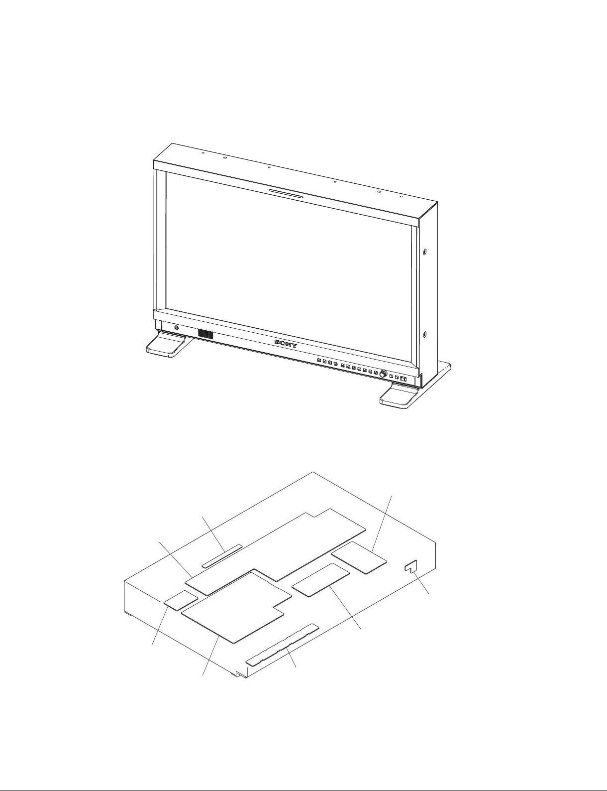
1-1. Appearance Figure
Section 1
Service Overview
1-2. Board Location
G1 board
G3 board
X board
QB board
G2 board
H2 board
BI board
H1 board
LMD-2041W
1-1 (E)
Page 10
1-3. Disassembly
m
. In this section, remove parts in the order of numbers shown in the fi gure.
. When removing/installing the cabinet and replacing the board, place the unit on the conductive cushion.
1-3-1. Rear Cover
5 Two screws
(B4 x 10)
9 Eleven screws
(3 x 6)
Upper side
7 Two screws
(3 x 6)
6 Two screws
(B4 x 10)
8 VESA bracket
0 Screw
(3 x 6)
!- Rear cover
3 Three screws
(B3 x 8)
1-2 (E)
Conductive cushion
4 Stand (*)
1 Three screws
(B3 x 8)
2 Stand (*)
*: Supplied with this unit
LMD-2041W
Page 11
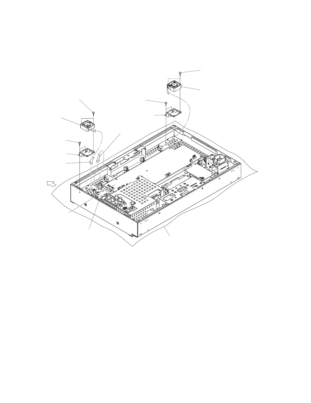
1-3-2. DC Fan
. Remove the rear cover. (Refer to Section 1-3-1.)
9 Two screws
(P3 x 20)
5 DC fan
2 Two screws
(PWH3 x 6)
3 Fan bracket
1 Harness
Upper side
4 Two screws
(P3 x 20)
J5
G3 board
7 Two screws
(PWH3 x 6)
8 Fan bracket
6 Harness
J1
0 DC fan
Conductive cushion
LMD-2041W
1-3 (E)
Page 12
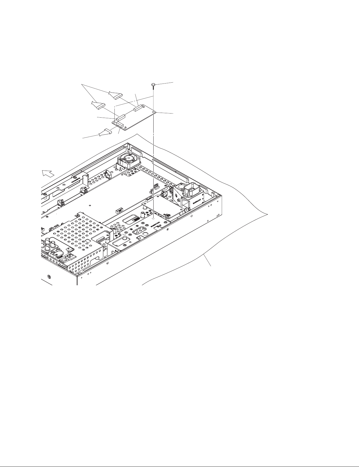
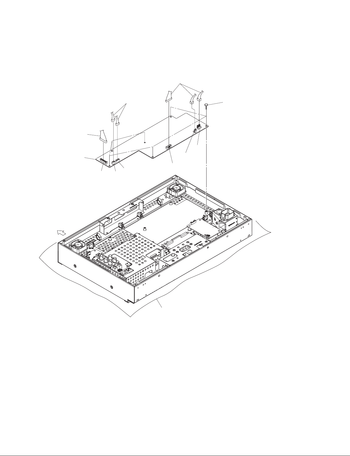
1-3-3. BI Board
. Remove the rear cover. (Refer to Section 1-3-1.)
2 Two harnesses
Upper side
1 Harness
J1
J4
J2
3 Two screws
(PWH3 x 6)
4 BI board
Conductive cushion
1-4 (E)
LMD-2041W
Page 13
1-3-4. G1 Board
. Remove the rear cover. (Refer to Section 1-3-1.)
3 Three harnesses
1 Harness
5 G1 board
Upper side
2 Two harnesses
CN702
J52
4 Six screws
(PWH3 x 6)
CN601
CN701
CN703
J51
LMD-2041W
Conductive cushion
1-5 (E)
Page 14

1-3-5. G2 Board
. Remove the rear cover. (Refer to Section 1-3-1.)
1 Harness
3 Two screws
(PWH3 x 6)
Upper side
CN801
4 G2 board
CN802
2 Flexible flat cable
Conductive cushion
1-6 (E)
LMD-2041W
Page 15

1-3-6. G3 Board
. Remove the rear cover. (Refer to Section 1-3-1.)
1 Two harnesses
J6
2 Harness
Upper side
J1
J5
J2
3 Two screws
(PWH3 x 6)
4 G3 board
2 Harness
LMD-2041W
Conductive cushion
1-7 (E)
Page 16
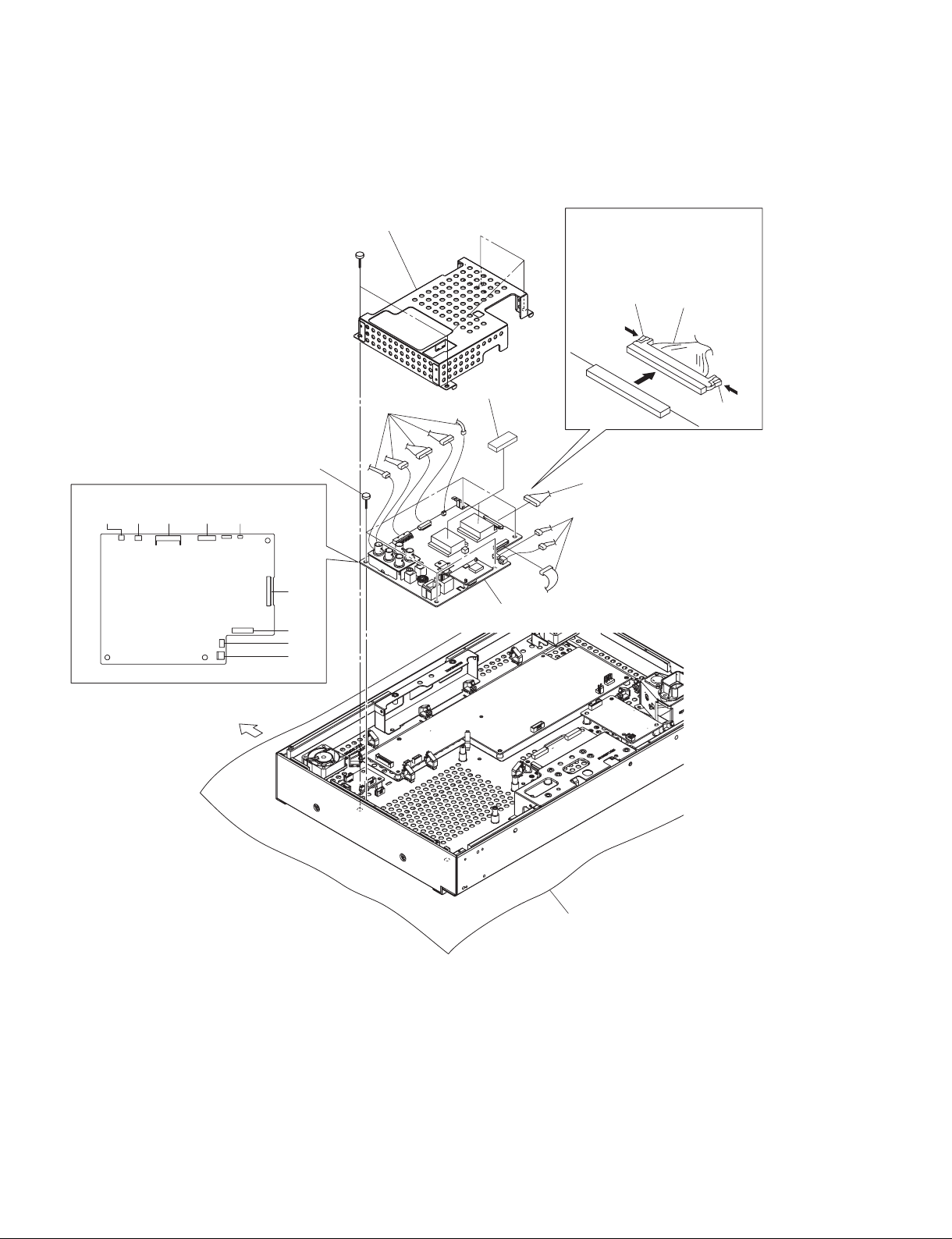
1-3-7. QB Board
. Remove the rear cover. (Refer to Section 1-3-1.)
7 QB board
J20J21 J14 J22 J7
1 Four screws
(PWH3 x 6)
6 Five screws
(PWH3 x 6)
J17
J9
J19
J18
2 QB shield assembly
3 Five harnesses
8 Two cushions
7 QB board
When removing the LVDS cable,
remove it in the direction of the
arrow C while holding the two
hooks in the direction of the
arrows A and B.
Hook
4 LVDS cable
A
C
4 LVDS cable
5 Three harnesses
B
Hook
Upper side
Conductive cushion
1-8 (E)
LMD-2041W
Page 17

1-3-8. Bezel Assembly
. Remove the rear cover. (Refer to Section 1-3-1.)
1 Harness
J7
7 Main frame assembly
J18
J19
QB board
J9
4 Two screws
(PWH3 x 6)
2 Two harnesses
3 Harness
5 Two screws
(3 x 6)
8 Bezel assembly
Upper side
6 Two screws
(3 x 6)
Conductive cushion
LMD-2041W
1-9 (E)
Page 18

1-3-9. H1 Board and X Board
. Remove the rear cover. (Refer to Section 1-3-1.)
. Remove the bezel assembly. (Refer to Section 1-3-8.)
!= Two screws
(B3 x 4)
!- Harness
![ X board
!] Tally cover
J1
Bezel assembly
2 Two screws
(B3 x 8)
4 H1 board
9 Standby button
7 Two hooks
3 Two screws
(PTPWH3 x 8)
5 Six hooks
8 Control keypad
assembly
1 Harness
J1
0 Encoder knob
6 Input keypad
assembly
Upper side
Conductive cushion
1-10 (E)
LMD-2041W
Page 19

1-3-10. H2 Board and Speaker
. Remove the rear cover. (Refer to Section 1-3-1.)
. Remove the bezel assembly. (Refer to Section 1-3-8.)
1 Harness
Bezel assembly
Upper side
3 Two screws
(TAPPING PWH2.5 x 6)
7 Two screws
(TAPPING PWH2.5 x 6)
8 Speaker
J1
6 H2 board
2 Screw
(B3 x 8)
4 Phone jack
bracket
5 Nut
LMD-2041W
Conductive cushion
1-11 (E)
Page 20

1-3-11. LCD Panel
. Remove the rear cover. (Refer to Section 1-3-1.)
. Remove the bezel assembly. (Refer to Section 1-3-8.)
3 Main frame
1 Two screws
(3 x 6)
6 LCD panel
2 Two screws
(3 x 6)
4 LVDS cable
Upper side
Conductive cushion
5 Flexible flat cable
When removing the LVDS cable, remove
it in the direction of the arrow C while
holding the two hooks in the direction of
the arrows A and B.
C
A
Hook
Hook
B
4 LVDS cable
1-12 (E)
LMD-2041W
Page 21

1-4. Software Update
1-4-1. System Software
Required equipment/tool
. Personal computer (hereafter referred to as PC)
. Connecting cable: Dedicated cable (1-831-247-11) and USB-serial conversion cable (for USB con-
nection).
. Writing application: Pixelworks FlashUpgrader
n
To obtain the writing application and the update fi le, please contact your local Sony Sales Offi ce/Service
Center.
Procedure
1. Create a folder at an arbitrary place on PC, and then store the writing application and the update fi le
in it. Turn off the power of PC.
2. Remove the screw, then remove the connector cover.
3. Connect the service connector (QB board) of this unit to PC as shown below.
Personal computer
USB-serial
conversion cable
Screw
Connector
cover
Service
connector
Dedicated cable
Rear surface of this unit
LMD-2041W
1-13 (E)
Page 22

4. Turn on the power of PC to start the writing application.
5. Select the connected serial port number of PC in the COM Port box.
n
To check the serial port number, select My Computer → Properties → Hardware tab → Device
Manager → Port (COM and LPT) on PC.
6. Check that only fl asher.hex and appcode.hex are displayed in the Files To Download box.
7. Click the [Flash] button.
“Waiting for target reset...” is displayed.
1-14 (E)
LMD-2041W
Page 23

8. Turn on the power of this unit.
The update is started and the progress bar is displayed.
After the update is completed, “Flash Completed!” is displayed and the area setting menu is displayed
on this unit.
9. Check SYS SW VERSION in VERSION INFO of the service menu.
LMD-2041W
1-15 (E)
Page 24

1-4-2. FPGA Software
Required equipment/tool
. RE connector assembly 9P (1-900-264-82)
. Personal computer (hereafter referred to as PC)
. Writing tool: Platform Cable USB manufactured by Xilinx
. Writing application: iMPACT (supplied with writing tool)
n
As for the writing application, refer to the Operating Instructions of the writing tool.
Connection
n
When connecting to the QB board and the BI board, remove the rear cover.
For the removal procedure of the rear cover, refer to Section 1-3-1.
For QB board
J15/QB board
Personal computer
For BI board
USB cable
(supplied with writing tool)
USB cable
(supplied with writing tool)
STATUS
indicator
Writing tool
QB board
Connecting
cable
Rear surface of this unit
J3/BI board
BI board
STATUS
indicator
Connecting
cable
Personal computer
1-16 (E)
Writing tool
Rear surface of this unit
LMD-2041W
Page 25

Preparation
n
It is the usage example of the writing software iMPACT Ver10.1.
1. Store the writing application and the update fi le in an arbitrary place on PC.
Turn off the power of PC.
2. Remove the rear cover from this unit. (Refer to Section 1-3-1.)
3. Connect each device as shown in Connection.
4. Turn on the power of each equipment.
5. Check that the STATUS indicator of the writing tool lights up green.
6. Start the writing application on PC.
The iMPACT Project window is displayed.
7. Select “create a new project (ipf)”, and then click the [OK] button.
iMPACT- Welcome to iMPACT window is displayed.
LMD-2041W
1-17 (E)
Page 26

8. Select “Confi gure devices using Boundary- Scan (JTAG)”, and then click the [Finish] button.
The Assign New Confi guration File window is opened.
Writing
1. QB board
1. Select the update fi le *****.mcs, and then click the [Open] button.
The Assign New Confi guration File window is opened.
n
***** represents the fi le name.
1-18 (E)
LMD-2041W
Page 27

2. Click the [Cancel] button.
The Device Programming Properties window is opened.
3. Click the [Cancel] button.
The iMPACT window is opened.
4. Check that the display of the Boundary Scan tab is as shown below.
Left device: xcf16p, *****.
Right device: xc3s2000
m
. The device name may vary depending on the confi guration.
. ***** represents the fi le name.
LMD-2041W
Boundary Scan tab
1-19 (E)
Page 28

5. Click the left device.
The display is changed to green.
6. Right-click on the left device, and then select Program.
1-20 (E)
LMD-2041W
Page 29

7. Place a check mark in the Verify check box, and then click the [OK] button.
The update is started. After it is completed, “Program Succeeded” is displayed.
8. Check FPGA VERSION in VERSION INFO of the service menu.
LMD-2041W
1-21 (E)
Page 30

2. BI board
1. Select the update fi le *****.mcs, and then click the [Open] button.
The Assign New Confi guration File window is opened.
n
***** represents the fi le name.
2. Click the [Cancel] button.
The Device Programming Properties window is opened.
1-22 (E)
LMD-2041W
Page 31

3. Click the [Cancel] button.
The iMPACT window is opened.
4. Check that the display of the Boundary Scan tab is as shown below.
Left device: xcf04s, *****_1
Center device: xcf04s, *****_0
Right device: xc3s1600e
n
Write the device of *****_1 to the left device and *****_0 the center device.
Boundary Scan tab
5. Click the left device.
The display is changed to green.
LMD-2041W
1-23 (E)
Page 32

6. Right-click on the left device, and then select Program.
7. Place a check mark in the Verify check box, and then click the [OK] button.
1-24 (E)
LMD-2041W
Page 33

The update is started. After it is completed, “Program Succeeded” is displayed.
8. Write to the center device in the same way as the left device. (Refer to steps 5 to 7.)
9. Check BI FPGA VERSION and BI SOFT VERSION in VERSION INFO of the service menu.
1-5. Lead-free Solder
Boards requiring use of lead-free solder are printed with a lead free mark (LF) indicating the solder
contains no lead.
(Caution: Some printed circuit boards may not come printed with the lead free mark due to their particular
size.)
: LEAD FREE MARK
m
. Be sure to use the lead-free solder for the printed circuit board printed with the lead free mark.
. The lead-free solder melts at a temperature about 40 dC higher than the ordinary solder, therefore, it is
recommended to use the soldering iron having a temperature regulator.
. The ordinary soldering iron can be used but the iron tip has to be applied to the solder joint for a slightly
longer time. The printed pattern (copper foil) may peel away if the heated tip is applied for too long, so
be careful.
LMD-2041W
1-25 (E)
Page 34

1-6. Circuit Description
1-6-1. G1 Board
The G1 board mounts the AC/DC converter and the DC/DC converter.
1-6-2. G2 Board
The G2 board is board for the LED backlight drivers.
1-6-3. G3 Board
The G3 board controls fans.
1-6-4. QB Board
The QB board performs input/output terminal, signal processing, audio processing and system control.
1-6-5. BI Board
The BI board controls T/C (Time code) and IMD (In-monitor display).
1-6-6. H1 Board
The H1 board mounts the control switches on the front panel.
1-6-7. H2 Board
The H2 board mounts a headphone output terminal.
1-6-8. X Board
The X board mounts a tally LED.
1-26 (E)
LMD-2041W
Page 35

Section 2
Electrical Alignments
2-1. Preparation
Required tools and measuring equipment
. Luminance meter: Konica Minolta Display color analyzer CA-310, CA-210, CA-110
or equivalent.
If none of them is available, make visual adjustment by comparing the LCD moni-
tor with the reference monitor that has already been calibrated correctly.
. Signal generator: Astrodesign VG-873, VG-854, Tektronix TG-700, or equivalent.
Warm-up time
Before starting adjustment, allow a warm-up of minimum 120 minutes to stabilize the back light of the
LCD panel.
How to enter service mode
1. Press the [MENU] button to display the MENU screen.
2. Press the [RETURN] and [F6] buttons simultaneously to enter the service mode.
How to exit the service mode
1. Press the [MENU] button to hide the MENU screen.
2-2. White Balance Adjustment
When replacing the LCD panel, perform the white balance adjustment.
1. Move the cursor to SIGNAL and press the [ENTER] button to enter the SIGNAL layer.
2. Move the cursor to WHITE BALANCE and press the [ENTER] button to enter the SIGNAL/WHITE
BALANCE layer.
Here, you can move the cursor and select the item by rotating and pressing the rotary encoder knob,
respectively.
When adjusting the D93
1. Set D93 in COLOR TEMP.
Target value : x = 0.283, y = 0.298
2. Adjust the highlight side in R Gain and B Gain.
3. Adjust the lowlight side in R BIAS and B BIAS.
4. Repeat steps 2 and 3 until all of the required specifi cations are met all at the same time.
LMD-2041W
2-1 (E)
Page 36

When adjusting the D65
1. Set D65 in COLOR TEMP.
Target value : x = 0.313, y = 0.329
2. Adjust the highlight side in R Gain and B Gain.
3. Adjust the lowlight side in R BIAS and B BIAS.
4. Repeat steps 2 and 3 until all of the required specifi cations are met all at the same time.
2-3. A/D Adjustment (COMPOSITE)
1. Input the NTSC 100% 8 color-bar COMPOSITE signal to this unit.
2. Press the COMPOSITE button to accept the COMPOSITE input signal.
Set NTSC SETUP to “0”.
3. Enter the service menu, then select SIGNAL → SIGNAL LEVEL → AUTO. Perform the following
automatic adjustments.
. Y/G LEVEL
. PB LEVEL
. PR LEVEL
4. Perform the adjustments of items 1-2 and 1-3 in table 1 by repeating the above described procedures.
As for 1-3, set NTSC SETUP to “7.5” before performing AUTO ADJ.
COMPOSITE selection input
1-1 NTSC SETUP 0 100% 8 color-bar signal
Y/G LEVEL
PB/B LEVEL
PR/R LEVEL
1-2 PAL 100% 8 color-bar signal
Y/G LEVEL
PB/B LEVEL
PR/R LEVEL
1-3 NTSC SETUP 7.5 100% 8 color-bar signal
Y/G LEVEL
PB/B LEVEL
PR/R LEVEL
Conditions:
NTSC SETUP 0
Conditions:
No specifi c conditions
Conditions:
NTSC SETUP 7.5
Table 1
2-2 (E)
LMD-2041W
Page 37

3-1. Backlight Does Not Light
Backlight does not light.
Section 3
Troubleshooting
Is harness
connected correctly?
Yes
Is the LED of
the standby switch lit?
No
Is the
backlight lit when
G1 board (in full working
order) is installed?
No
Yes
Yes
No
Connect the harness
correctly.
Replace the QB board.
(Refer to Section 1-3-7.)
Replace the G1 board.
(Refer to Section 1-3-4.)
Is the
backlight lit when
G2 board (in full working
order) is installed?
Replace the LCD panel.
(Refer to Section 1-3-11.)
LMD-2041W
No
Yes
Replace the G2 board.
(Refer to Section 1-3-5.)
3-1 (E)
Page 38

3-2. System Does Not Start
System does not start.
Is harness
connected correctly?
Yes
Is the LED of
the standby switch lit?
No
Is the
symptom improved
when G1 board (in full
working order) is
installed?
No
Is the
symptom improved
when G2 board (in full
working order) is
installed?
No
Replace the LCD panel.
Yes
Yes
Yes
No
Connect the harness
correctly.
Replace the QB board.
(Refer to Section 1-3-7.)
Replace the G1 board.
(Refer to Section 1-3-4.)
Replace the G2 board.
(Refer to Section 1-3-5.)
3-3. Control Operation of This Unit Is Abnormal
Control operation of this unit is
abnormal.
Is harness
connected correctly?
Yes
Is the symptom
improved by the external
operation of PARALLEL
REMOTE connector?
Yes
Replace the H1 board.
(Refer to Section 1-3-9.)
3-2 (E)
No
No
n
For the external operation of PARALLEL REMOTE connector,
refer to the Operating Instructions.
Connect the harness
correctly.
Replace the QB board.
(Refer to Section 1-3-7.)
LMD-2041W
Page 39

3-4. Image Is Abnormal
Image is abnormal.
Is harness
connected correctly?
Yes
Is the
symptom improved
when BI board (in full
working order) is
installed?
No
Is the
symptom improved
when QB board (in full
working order) is
installed?
No
Replace the LCD panel.
(Refer to Section 1-3-11.)
No
Yes
Yes
3-5. TALLY Lamp Is Not Lit
Connect the harness
correctly.
Replace the BI board.
(Refer to Section 1-3-3.)
Replace the QB board.
(Refer to Section 1-3-7.)
TALLY lamp is not lit.
Is harness
connected correctly?
Is the
symptom improved
when X board (in full
working order) is
installed?
Replace the QB board.
(Refer to Section 1-3-7.)
LMD-2041W
Yes
No
Yes
No
Connect the harness
correctly.
Replace the X board.
(Refer to Section 1-3-9.)
3-3 (E)
Page 40

3-6. Fan Is Abnormal
Fan is abnormal.
Is harness
connected correctly?
Yes
Replace the abnormal fan.
(Refer to Section 1-3-2.)
Is the symptom improved?
No
Is the
symptom improved
when G3 board (in full
working order) is
installed?
No
No
Yes
Yes
Connect the harness
correctly.
No problem.
Replace the G3 board.
(Refer to Section 1-3-6.)
Replace the QB board.
(Refer to Section 1-3-7.)
3-4 (E)
LMD-2041W
Page 41

Section 4
Spare Parts
4-1. Notes on Repair Parts
1. Safety Related Components Warning
w
Components marked ! are critical to safe operation.
Therefore, specifi ed parts should be used in the case of
replacement.
2. Standardization of Parts
Some repair parts supplied by Sony differ from those
used for the unit. These are because of parts commonality and improvement.
3. Stock of Parts
Parts marked with “o” at SP (Supply Code) column of
the spare parts list may not be stocked. Therefore, the
delivery date will be delayed.
4. Harness
Harnesses with no part number are not registered as
spare parts.
4-1. 補修部品注意事項
1. 安全重要部品
! 警告
! 印のついた部品は安全性を維持するために重要
な部品です。したがって,交換する時は必ず指定
の部品を使ってください。
2. 部品の共通化
ソニーから供給する補修用部品は,セットに使われて
いるものと異なることがあります。
これは部品の共通化,改良等によるものです。
3. 部品の在庫
部品表の SP(Supplycode)欄に“o”で示される部品は
在庫していないことがあり,納期が長くなることがあ
ります。
4. ハーネス
部品番号の記載されていないハーネスは,サービス部
品として登録されていません。
The components identifi ed by mark contain confi dential
information.
Strictly follow the instructions whenever the components
are repaired and/or replaced.
印の部分には,秘密情報が含まれています。
修理の際は,指示に従った対応を行ってください。
LMD-2041W
4-1
Page 42

Cover Block
4-2. Exploded Views
21
B4 x 10
22
21
B4 x 10
20
21
3
PWH3 x 6
PWH3 x 6
9
B3 x 8
12
13
2
PTPWH
3 x 8
15
8
5
1
B3 x 8
10
4
TAPPING
PWH2.5 x 6
TAPPING
PWH2.5 x 6
21
18
21
B3 x 8
11
7
B3 x 8
B3 x 4
6
PTPWH
3 x 8
16
21
PTPWH
3 x 8
21
17
14
B3 x 8
*
*
23
21
19
14
B3 x 8
* : Supplied accessory
4-2
LMD-2041W
Page 43

No. Part No. SP Description
1 X-2560-420-1 s KEYPAD ASSY, INPUT
2 X-2580-278-1 s KEYPAD ASSY, CONTROL
3 X-2583-530-1 s COVER ASSY, REAR
4 1-857-413-11 s MOUNTED CIRCUIT BOARD, H2
5 1-857-863-11 s MOUNTED CIRCUIT BOARD, H1
6 1-857-864-11 s MOUNTED CIRCUIT BOARD, X
7 1-858-749-11 s SPEAKER
8 1-910-401-91 o CONNECTOR ASSY DF13 15P
9 1-910-401-92 o CONNECTOR ASSY SHR 3P
10 1-910-401-95 o CONNECTOR ASSY DF13 4P
11 3-061-234-01 s NUT (M6X0.5)
12 4-146-124-01 s BUTTON, STANDBY
13 4-146-125-02 s KNOB, ROTARY ENCODER
14 4-262-134-01 s COVER, MYLAR
15 4-262-141-01 s SHIELD, KEYPAD
16 4-414-978-01 s BEZEL(TOP)
17 4-414-979-01 s BEZEL(BTM)
18 4-414-980-01 s BEZEL(LEFT)
19 4-414-981-01 s BEZEL(RIGHT)
20 4-414-985-01 s BRACKET, VESA
21 4-670-040-02 s SCREW
22 4-414-986-01 s LABEL, CONTROL
Cover Block
7-681-000-61 s TAPPING +PWH 3X8 TYPE2 N-S
7-682-146-13 s SCREW +P 3X5
7-682-545-09 s SCREW +B 3X4
7-682-562-09 s SCREW +B 4X10
7-682-903-19 s SCREW +PWH 3X6
7-685-902-01 s TAPPING +PWH 2.6X5 TYPE2 N-S
LMD-2041W
4-3
Page 44

Chassis Block
110
E
113
PWH
B
3 x 6
C
D
101
PWH
3 x 6
J
G
E
F
114
116
D
119
PWH
3 x 10
F
A
108
PWH
3 x 6
104
112
P3 x 20
106
PWH
121
3 x 6
PWH
H
3 x 6
107
PWH
3 x 6
109
111
122
118
G
PWH
A
115
PWH
PWH
3 x 6
3 x 6
105
PWH
3 x 6
P3 x 20
103
H
J
123
3 x 6
120
B
C
123
4-4
117
102
124
LMD-2041W
Page 45

No. Part No. SP Description
101 ! 1-576-231-51 s FUSE (H.B.C.) (4A/250V)
102 ! 1-811-502-11 s MODIFIED LCD PANEL
103 ! 1-855-155-11 s D.C. FAN
104 ! 1-855-155-21 s D.C. FAN
105 1-857-860-11 s MOUNTED CIRCUIT BOARD, BI
106 1-895-156-11 s MOUNTED CIRCUIT BOARD, G3
107
1-895-004-31 s MOUNTED CIRCUIT BOARD, QB
108 ! 1-895-125-11 s MOUNTED CIRCUIT BOARD, G1
109 1-895-126-11 s MOUNTED CIRCUIT BOARD, G2
110 1-910-400-62 o CONNECTOR ASSY DF13 3P
111 1-910-400-69 o CONNECTOR ASSY XLR
112 1-910-401-27 o CONNECTOR ASSY, DF13 2-3P
113 1-910-401-90 o CONNECTOR ASSY PHDR 24P
114 1-910-401-93 o CONNECTOR ASSY DF13 12P
115 1-910-401-94 o CONNECTOR ASSY PHR 5P
116 1-910-401-96 s CONNECTOR ASSY LVDS 40-30P
117 1-910-401-97 s CONNECTOR ASSY LVDS 40P
118 ! 1-910-401-98 s CONNECTOR ASSY AC INLET
119 1-910-401-99 o CONNECTOR ASSY PAP 8P
120 2-434-609-11 s SCREW (M4X8 CR)
121 2-990-241-02 s HOLDER (A), PLUG
122 4-148-038-01 s SCREW F 2.5X6
123 4-670-040-02 s SCREW
124 9-885-165-31 s FLEXIBLE FLAT CABLE
Chassis Block
7-682-153-01 s SCREW +P 3X20
7-682-545-09 s SCREW +B 3X4
7-682-548-09 s SCREW +B 3X8
7-682-903-19 s SCREW +PWH 3X6
7-682-903-39 s SCREW +PWH M3X10
LMD-2041W
4-5
Page 46

4-3. Packing Materials & Supplied
Accessories
---------------------------------------PACKING MATERIALS & SUPPLIED ACCESSORIES
--------------------------------------- Ref. No.
or Q'ty Part No. SP Description
2pcs A-1860-455-A s STAND COMPLETE ASSY
1pc 2-990-242-01 s HOLDER (B), PLUG
1pc 4-256-685-03 s OPERATING INSTRUCTIONS
(JAPANESE, ENGLISH)
1pc 4-256-686-03 s CD-ROM
OPERATING INSTRUCTIONS
(JAPANESE, ENGLISH, FRENCH,
GERMAN, ITALIAN, SPANISH,
SIMPLIFIED CHINESE, TRADITIONAL
CHINESE, KOREAN)
MANUAL, INTERFACE
(JAPANESE, ENGLISH)
2pcs 4-414-990-01 s MOUNTING BRACKET
6pcs 7-682-548-09 s SCREW +B 3X8
8pcs 7-682-561-09 s SCREW +B 4X8
4-6
LMD-2041W
Page 47

Section 5
Block Diagrams
OverallOverall
SERIAL
REMOTE
FOR
SERVICE
SDI1
SDI2
SDI OUT
COMPOSITE
COMPOSITE
OUT
HDMI IN
H2
HEAD
PHONE
AUDIO IN
AUDIO OUT
QB
SDI_OUT
IN
D0_ to D2_,D0+ to D2+,CK+,CK_
SPEAKER+
SPEAKER_
PHONE_ROUT
PHONE_LOUT
PHONE_DET
AUDIO_A_INR
AUDIO_A_INL
AUDIO_OUT_R
AUDIO_OUT_L
EQ
EQ
CD
TXO+
TXO_
75
RXO+
RXO_
RELOCKER
Z
24.576MHz
28.6368MHz
SDI
EQ
SDO
/SDO
27MHz
AUDIO
AUDIO
PROCESSOR
SDI
SDIb
AMP
AUDIO_R
AUDIO_L
SDI DES
VIDEO
DECODER
HDMI RX
EPR
SPI_TDI1_GS2965
SPI_CS1_GS2965
SPI_TDO
SPI_SCLK
SDI_DOUT[0-19]
SDI_CLK
SDI_HS
SDI_VS
SDI_FD
SDI_MCLK
SDI_LRCK
SDI_BICK
SDI_SDTI_0-3
SPI_CS0_GS2970
SPI_TDI0_GS2970
DEC_Y[0-9]
DEC_U[0-9]
DEC_V[0-9]
DEC_CLK
DEC_HSOUT
DEC_VSOUT
DEC_FIELD
DEC_ACT
HDMI_YG[0-9]
HDMI_UB[0-9]
HDMI_VR[0-9]
HDMI_CLK
HDMI_HSYNC
HDMI_VSYNC
HDMI_DE
HDMI_FIELD
HDMI_MCLK
HDMI_BICK
HDMI_LRCK
HDMI_SDTI
J15
8 PIN
PROM_TDO
CN
TDI
AUDIO_D_INR
AUDIO_D_INL
FPGA
PROM_TCK
PROM_TMS
PROM_TDI
PROM_D[0-7]
PROM
PROG_B
PROM_CLK
DONE
DAC
UART_TX
UART_RX
INV
RS232_SEL
25.175MHz
OVD_A_YG_[0-9]
OVD_A_UB_[0-9]
OVD_A_VR_[0-9]
OVD_A_HS
OVD_A_VS
OVD_A_CK
OVD_A_DE
OVD_A_VBI
OVD_A_FD
OVD_A_SG
OVD_B_YG_[0-9]
OVD_B_UB_[0-9]
OVD_B_VR_[0-9]
OVD_B_HS
OVD_B_VS
OVD_B_CK
OVD_B_DE
OVD_B_VBI
OVD_B_FD
OVD_B_SG
OAD_MCLK
OAD_BICK
OAD_SDTI
OAD_LRCK
DAC_PDN
DAC_MUTE
DAC_DFS
DAC_DIF
DAC_DZF
PHONE_DET
TRANCEIVER
PAR_PIN1
PAR_PIN2
PAR_PIN3
PAR_PIN4
PAR_PIN6
PAR_PIN7
PAR_PIN8
RS-232
RX_SP
TX_SP
MPX
SCALER
I/O
PAR_PIN7_SW
SW
TXO+
TXO_
TRANSFORMER
RXO+
RXO_
TXD_ETHERNET
RXD_ETHERNET
TALLY_EN_HW
PAR_PIN8_SW
PAR_PIN7_HW
TPOP
TPON
TPIP
TPIN
ETHERNET
BOARD
PMT
PPAT
TX_SW2
RX_SW2
RX_PW318
TX_PW318
ROTARY_A,ROTARY_B,ROTARY_INT
BL_ON,BL_CTL_PWM
TCON_ON
SDA_3.3V,SCL_3.3V
A[1-21]
D[0-15]
16 x 16M
TXE0_/TXE0+
TXE1_/TXE1+
TXE2_/TXE2+
TXE3_/TXE3+
TXE4_/TXE4 +
TXECK_/TXECK+
TXO0_/TXO0+
TXO1_/TXO1+
TXO2_/TXO2+
TXO3_/TXO3+
TXO4_/TXO4+
TALLY_G
TALLY_R
PAR_PIN8_HW
DONE_FPGA2
+3.3V_ETH,+2.5V_ETH
ON_ETH
RED_LED_ON
ETH_INT
Flash
16M
DDR
x 2
+3.3VA
SDA_FPGA
SCL_FPGA
RST_IMDSYS
TX_IMD
RX_IMD
J17
J22
SENSOR
SW
X
TALLY RED
TALLY GREEN
TEMP
RX_IMD
TX_IMD
BI
J1
V_TCON
LVDS
OSD
CTRL
J4
+3.3VA
SDA_FPGA
SCL_FPGA
DONE_FPGA2
RST_IMDSYS
TX_IMD
RX_IMD
G3
FAN
CTRL
32.768kHz
G1
+5V,+9V,+3.3VA
H1
I
IPD_R1[0-7]
IPD_G1[0-7]
IPD_B1[0-7]
IPD_R2[0-7]
IPD_G2[0-7]
IPD_B2[0-7]
I/F
IPD_HSYNC
IPD_VSYNC
IPD_DE
IPD_CLK
OSD_DAI[3-0]
OSD_DBI[3-0]
OSD_CLKI
OSD_CLKO
OSD_HSO_X
OSD_VSO_X
OSD_DISPO
OSD_ENAI
OSD_ENBI
2
C I/O
SCI
STANDBY
POWER
POWER IC
2
I
DIMMER
FAN
DRV
FAN
DRV
C BUS,
LED
FPGA
+9V,+5V,SDA_3.3VA, SCL_3.3VA
FAN
FAN
POWER
+
5V_PANEL
ROTARY
ENCODER
OPD_R1[0-7]
OPD_G1[0-7]
OPD_B1[0-7]
OPD_R2[0-7]
OPD_G2[0-7]
OPD_B2[0-7]
OPD_HSYNC
OPD_VSYNC
OPD_DE
OPD_CLK
RAM_DQ[0-15]
RAM_ADO[0-11]
RAM_DQML
RAM_DQMH
RAM_CAS
RAM_RAS
CLK
CKE
CS
WE
PROM
LVDS
I/F
4Mx16
SDRAM
BL_ON, BL_ADJ
ODDEVEN
PROM
AC/DC
G2
LED BACKLIGHT
CONTROLLER
J2
AC IN
DC IN
ISEN
LCD
PANEL
LMD-2041W
PARALLEL
REMOTE
5-1
Overall
5-1
Page 48

Page 49

J6
Frame WiringFrame Wiring
Section 6
Frame Wiring
1
CN601
!
AC IN
CN701
DC IN
J51
G3
J5
!
FAN
J2
J1
!
FAN
J21
J52
J20
CN702
J14
J7
J15
FOR
SERVICE
J17 J1
J22 J4
G2
CN703
CN801
J1
CN802
!
G1
2
!
LCD
PANEL
X
3
J2
J3
FOR
SERVICE
BI
J19
J2
H2
Note: The components identified by mark contain
confidential information.
Strictly follow the instructions whenever the
components are repaired and/or replaced.
QB
J18
SPEAKER
J9
J1
H1
Frame Wiring
LMD-2041W
A B C D E F G H
6-1
6-1
4
5
Page 50

Page 51

Page 52

LMD-2041W (CN)
LMD-2041W (SY) J, E
9-968-890-01
Sony Corporation
Printed in Japan
2011. 11 32
©2011
 Loading...