

Page 1
SERVICE MANUAL
MODEL COMMANDER DEST. CHASSIS NO.
RE-3W
CHASSIS
KP-44PS2 RM-903 AEP SCC-P38E-A
KP-44PS2U RM-903 UK SCC-P64A-A
KP-51PS2 RM-903 AEP SCC-P38D-A
TV
D
O
I
E
V
1
2
3
4
5
6
7
8
9
0
PROGR
MENU
RM
S
RM-903
903
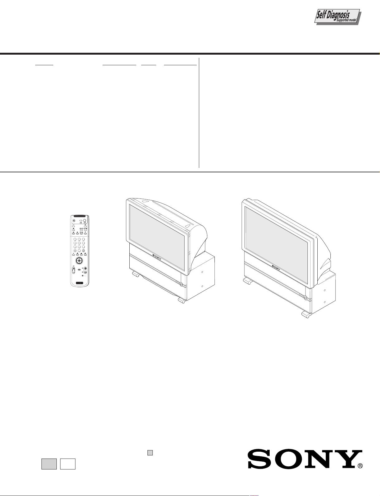
KP-44PS2/44PS2U
KP-51PS2
∗ Please file according to model size. ...
44
51
PROJECTION TV
Page 2

KP-44PS2/44PS2U/51PS2
RM-903
SPECIFICATIONS
TV system
B/G/H, D/K, I, L
Colour system
PAL, SECAM
NTSC 3.58, 4.43 (only Video In)
Channel coverage
VHF: E2-E12
UHF: E21-E69
CATV: S1-S20
HYPER: S21-S41
D/K: R1-R12, R21-R69
I: UHF B21-B69
L: F2-F10, B-Q, F21-F69
Projected picture size
KP-44PS2/44PS2U:
44 inches (approx. 112 measured diagonally).
KP-51PS2:
51 inches (approx. 130 measured diagonally).
Rear Terminals
C
• Centre speaker input terminals (2
terminals)
• (L, R) audio outputs (phono jacks)
• i1/ 21-pin Euro connector (CENELEC
standard)
including audio/video input, RGB
input,
TV audio/video output.
• i2/r 2 21-pin Euro connector (CENELEC
(SMARTLINK)
• i3/r 3 21-pin Euro connector (CENELEC
Front Terminals
r 4 S video input - 4 pin DIN
t 4 video input - phono jack
4 audio inputs - phono jacks
Headphones jack - minijack stereo
standard) including audio/video
input, S video input,
selectable audio/video output and
Smartlink interface.
standard)
including audio/video input, S video
input,
audio/video output (monitor out).
Sound output
2 x 30 W (music power)
2 x 15 W (RMS)
Centre SP input
30 W (RMS) (using as the centre speaker)
Power consumption
225 W
Standby Power consumption
< 0.7 W
Dimensions (w x h x d)
KP-44PS2/44PS2U: Approx. 1100 x 1161 x 543 mm
KP-51PS2: Approx. 1256 x 1264 x 633 mm
Weight
KP-44PS2/44PS2U: Approx. 87 kg
KP-51PS2: Approx. 97 kg
Accessories supplied
1 Remote Control (RM-903)
2 Batteries (IEC designated)
Other features
DRC 100 Hz picture
Digital Comb filter (High resolution)
TELETEXT, Fastext, TOPtext (2000 page TEXT memory)
NexTView
NICAM
Sleep Timer
Smartlink
Digital Noise detection
Graphic Equaliser
Personal ID
Auto Format
Design and specifications are subject to change without notice.
CAUTION
SHORT CIRCUIT THE ANODE OF HTE PICTURE TUBE
AND THE ANODE CAP TO THE METAL CHASSIS, CRT
SHIELD, OR CARBON PAINTED ON THE CRT, AFTER
REMOVING THE ANODE.
SAFETY-RELATED COMPONENT WARNING!!
COMPONENTS IDENTIFIED BY SHADING AND MARK
! ON THE SCHEMATIC DIAGRAMS, EXPLODED
VIEWS AND IN THE PARTS LIST ARE CRITICAL TO
SAFE OPERATION. REPLACE THESE COMPONENTS
WITH SONY PARTS WHOSE PART NUMBERS APPEAR AS SHOWN IN THIS MANUAL OR IN SUPPLEMENTS PUBLISHED BY SONY.
– 2 –– 2 –
Page 3

TABLE OF CONTENTS
1. SELF DIAGNOSIS FUNCTION
1-1. RE-3W Self Diagnostic Software ...................... 4
1-2. Error Detection Monitor..................................... 5
1-2-1. Error Monitor Menu....................................... 5
1-2-2. Error Reader Display ..................................... 6
2. GENERAL ................................................................. 7
3. DISASSEMBLY
3-1. Rear Board Removal ......................................... 21
3-2. Main Bracket Block Removal ........................... 21
3-3. Service Position ................................................. 21
3-4. Control Panel Block Removal .......................... 22
3-5. Resistor Assembly (Focus Pack) Removal ....... 22
3-6. HB, HA and Control Panel Block Removal ...... 23
3-7. Beznet Block Removal ...................................... 23
3-8. Chassis Block Removal...................................... 24
3-9. Terminal Board Removal ................................... 25
3-10. AP and D Boards Removal ................................ 25
3-11. G Board Removal ............................................... 26
3-12. J, B3, E, M and S Boards Removal ................... 26
3-13. A Board Removal ............................................... 27
3-14. High-Voltage Cable Removal and Installation.. 27
3-15. Picture Tube Removal ........................................ 27
4. SET-UP ADJUSTMENTS
4-1. Screen Voltage Adjustment
(Rough Alignment) ........................................... 28
4-2. Screen (G2) Adjustment .................................... 28
4-3. Focus Rough Adjustment .................................. 28
4-4. Deflection Yoke Tilt Adjustment ...................... 28
4-5. 2-Pole Magnet Adjustment ................................ 29
4-6. 4-Pole Magnet Adjustment ................................ 29
4-7. Green, Red and Blue Focus Adjustment............ 29
4-7-1. Green, Red and Blue Lens Focus
Adjustment .................................................... 29
4-7-2. Green, Red and Blue Electrical Focus
Adjustment .................................................... 29
5. SAFETY RELATED ADJUSTMENT
5-1. HV Hold-Down Adjustment ............................. 30
6. ELECTRICAL ADJUSTMENTS
6-1. Adjustments with Commander .......................... 31
6-1-1. How to Select Each Mode ............................. 31
6-1-2. How to Enter TT Mode .................................. 31
6-1-3. How to Enter Service Menu .......................... 31
6-1-4. Screen Display for Service Menu .................. 32
6-1-5. Service List (Projector Engine) ..................... 37
6-2. Registration Adjustment .................................... 39
KP-44PS2/44PS2U/51PS2
RM-903
Section Title PageSection Title Page
6-2-1. Setup for Adjustment ..................................... 39
6-2-2. Main Deflection Adjustment ......................... 39
6-2-3. Operation Method for
Projector Engine Mode .................................. 40
6-2-4. Projector Engine Adjustment
(Sub Deflection Adjustment)......................... 41
6-3. Auto Convergence Offset................................... 44
6-4. Picture Center Adjustment ................................. 44
6-5. White Balance Adjustment ................................ 44
6-6. Sub Bright Adjustment....................................... 45
6-7. Sub Color Adjustment........................................ 45
6-8. Auto Convergence Error Code List ................... 46
6-9. Test-Test Mode................................................... 47
7. DIAGRAMS
7-1. Block Diagrams .................................................. 49
7-2. Frame Schematic Diagram................................. 75
7-3. Circuit Boards Location ..................................... 78
7-4. Schematic Diagrams and Printed Wiring
Boards ................................................................. 79
(1) Schematic Diagram of J (1/2) Board ................. 80
(2) Schematic Diagram of J (2/2) Board ................ 83
(3) Schematic Diagram of A Board ........................ 91
(4) Schematic Diagram of B3 (1/5) Board .............. 94
(5) Schematic Diagram of B3 (2/5) Board .............. 97
(6) Schematic Diagram of B3 (3/5) Board .............. 100
(7) Schematic Diagram of B3 (4/5) Board .............. 103
(8) Schematic Diagram of B3 (5/5) Board .............. 107
(9) Schematic Diagram of HA and HB Boards ....... 109
(10) Schematic Diagram of E Board ......................... 113
(11) Schematic Diagram of AP Board....................... 117
(12) Schematic Diagram of D Board ......................... 120
(13) Schematic Diagrams of CR, CG, CB, ZR, ZG
and ZB Boards.................................................... 129
(14) Schematic Diagram of M Board ........................ 132
(15) Schematic Diagram of S Board.......................... 135
(16) Schematic Diagram of G Board ......................... 138
7-5. Semiconductors ................................................. 143
7-6. IC Block Diagrams............................................. 146
8. EXPLODED VIEWS
8-1. Screen and Cover Block (KP-44) ..................... 149
8-2. Control Panel and Cabinet Block (KP-44) ....... 150
8-3. Screen and Cover Block (KP-51) ...................... 151
8-4. Control Panel and Cabinet Block (KP-51) ........ 152
8-5. Main Bracket Block ........................................... 153
8-6. Picture Tube Block............................................. 154
9. ELECTRICAL PARTS LIST ............................ 155
– 3 –– 3 –– 3 –
Page 4
KP-44PS2/44PS2U/51PS2
RM-903
SECTION 1
SELF DIAGNOSIS FUNCTION
1-1. RE-3W SELF DIAGNOSTIC SOFTWARE
The identification of errors within the RE-3W chassis is triggered in one of two ways : - 1: Busy or 2: Device failure to respond to IIC.
In the event of one of these situations arising the software will first try to release the bus if busy (Failure to do so will report with a
continuous flashing LED) and then communicate with each device in turn to establish if a device is faulty. If a device is found to be
faulty the relevant device number will be displayed through the LED (Series of flashes which must be counted) See table 1., non fatal
errors are reported using this method.
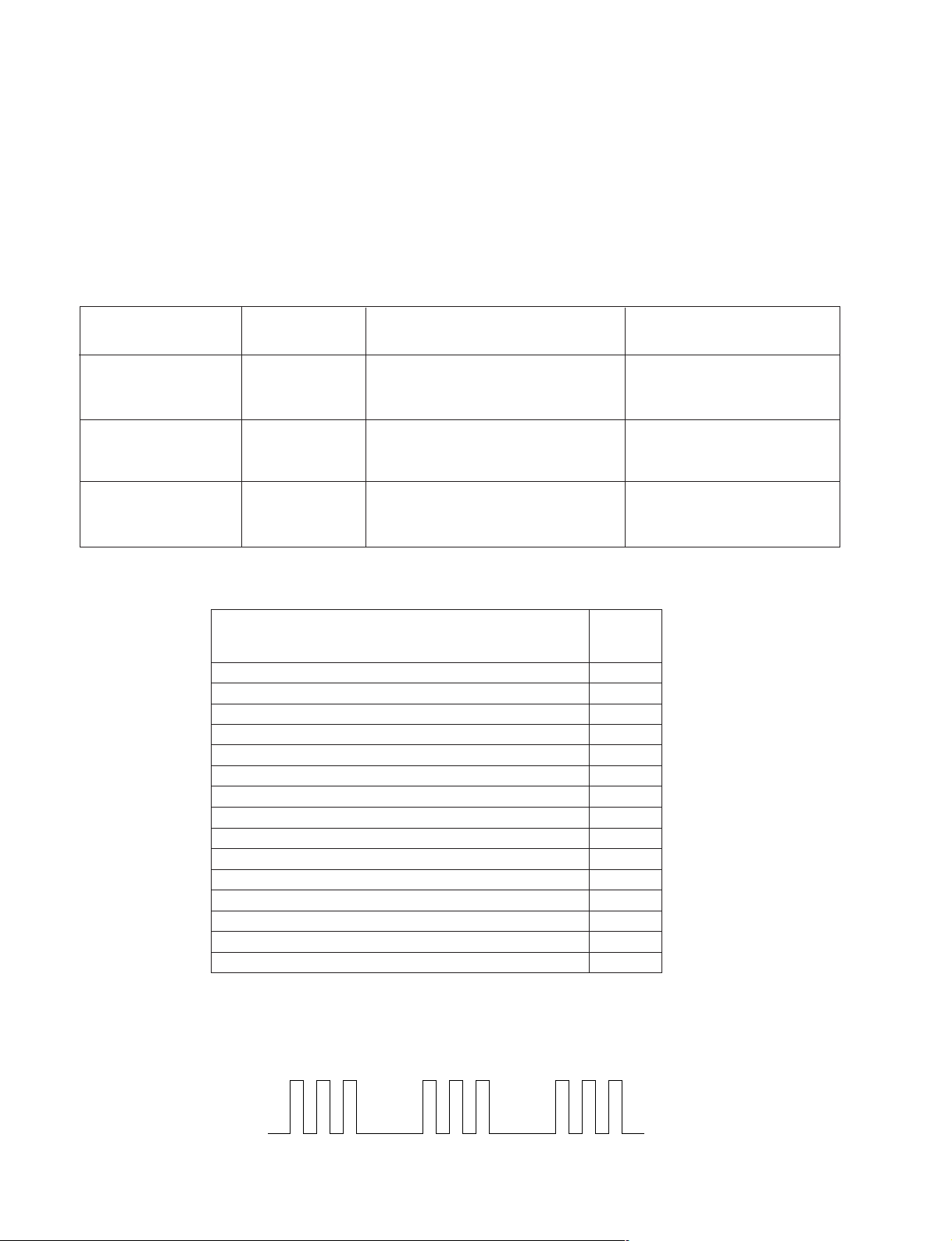
Diagnostic Item
Description
Power does not turn on Does not light
+B Overcurrent (OCP) 2 times Linearity FET (Q5105) is shorted (D Board)
Vertical Deflection stopped 4 times –15 V is not supplied R5341 open (D Board)
No. of times Standby
LED Flashes
Probable cause Location
Power cord is not plugged in
Fuse is open circuit
H. OUT (Q5104) is shorted (D Board)
IC6004 Power IC is shorted (G Board)
+15 V is not supplied R5340 open (D Board)
IC5302 is shorted (D Board)
ERROR ERROR
COUNT
No error 00
Not allowed (may be confused with Sircs response flash) 01
Over Current Protection 02
Over Voltage Protection 03
Vertical Protection 04
Not used 05
Horizontal Protection 06
Speaker Protection 07
General IIC Line 0 error 08
MEGATEXT (IC9502) 09
NVM (IC9108) 10
Main colour decoder (IC8301) 11
Backend (IC4301) 14
Multi sound processor (IC4702) 15
External RAM (IC9107) 17
Detected Symptoms
Power does not come on
No power is supplied to the TV
AC power supply is faulty
Power does not come on
Load on power line has shorted
Vertical deflection pulse has stopped
Power line has shorted
LED
Flash Timing Example : e.g. error number 3
ON
OFF OFF
ON ONStandby LED
– 4 –
Page 5

KP-44PS2/44PS2U/51PS2
1-2. ERROR DETECTION MONITOR
Device acknowledge is used to check IIC errors. Device acknowledge is checked by sending an IIC start sequence during CRT power
on. Each device is checked three times, if there is no acknowledge after each attempt, it will be regarded as an error.
There are three steps to check for errors.
1. IIC line 0
If all devices except the NVM have errors, IIC line 0 error is displayed.
2. Board check
If all devices mounted on one board have errors, board error is displayed.
3. Each device check
if IIC line error and board error are not detected then the device with an error is displayed.
The detected errors can be displayed as follows:
1. Error Monitor Menu
2. Error Reader
RM-903
1-2-1. Error Monitor Menu
The error monitor menu is displayed by selecting TT33. The following menu will be displayed:
Error Monitor
Ignore Errors OFF
1
Operating Time :
Stored Errors :
1. A-Board
2. B3-B CXA2100 MID
3. J-B CXA2123 Main Col Dec
4. Error Code Not Valid
5. Error Code Not Valid
Current Error :
Start Error Sequence
000021 h 40 min
ON ON
– 5 –
Page 6
KP-44PS2/44PS2U/51PS2
RM-903
1-2-2. Error Reader Display
The error reader display is connected to the service connector to read actual error codes. The part number for the error reader display
is S-188-900-10.
Once an error has been detected it will then be displayed on the two digit error reader. The errors displayed refer to the following table:
Send Data to Error Reader
Error Code Data High Data Low Error Type Function
00 00h – f0h no device
Gen. IIC Error
00 01h f0h 01h IIC 0 line
00 02h f0h 02h IIC 1 line not used
Board Error
01 00h f1h 00h A Board
04 00h f4h 00h B3 Board
06 00h f6h 00h E Board
07 00h f7h 00h J/S Board
08 00h f8h 00h M Board
Device Error
A Board
01 01h f1h 01h CXA1875 Port Expander
01 02h f1h 02h TU1301 Main Tuner
01 03h f1h 03h TU1302 Sub Tuner
B3 Board
04 01h f4h 01h CXD9509 MID
E Board
06 01h f6h 01h CXA2100 Backend
J Board
04 04h f4h 04h TDA9178 Picture Booster
07 01h f7h 01h CXA2057 Auto Wide
07 03h f7h 03h CXA2123 Sub Colour
07 04h f7h 04h CXA2123 Main Colour
07 0Ah f7h 0Ah CXA2149 AV SW
S Board
07 05h f7h 05h CXA1875 Sub Sound
07 08h f7h 08h MSP3410D Sound Proc
M Board
08 01h f8h 01h ST24C32 NVM
– 6 –
Page 7
The operating instructions mentioned here are partial abstracts
5
GB
One Remote Control
(RM-903)
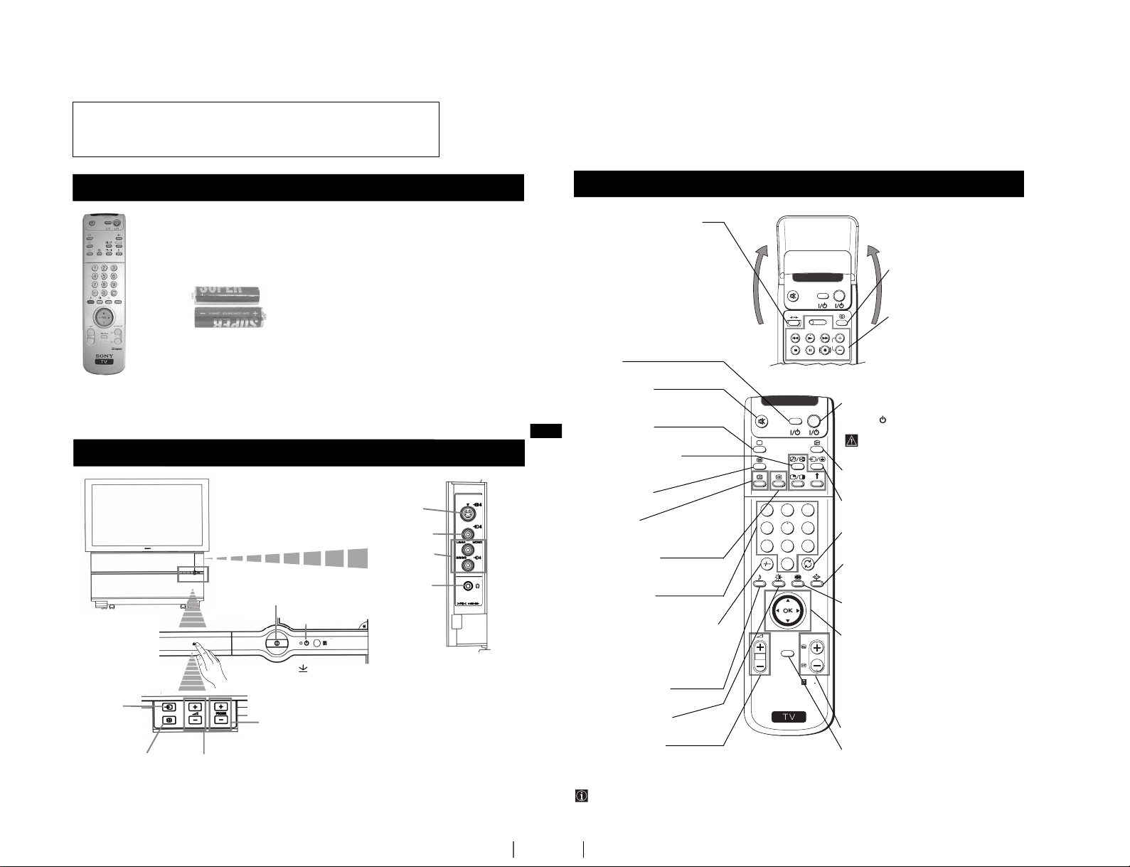
Overview of TV Buttons
Checking the Accessories Supplied
Overview
Two batteries (R6 type)
Overview
s
Programme up
or down buttons
(selects TV channels)
On/Off Switch
Selecting
input source
Auto
Convergence
button
Volume control
buttons
Press on the mark , on the front
of the projection TV to reveal the front
buttons.
Standby indicator
S Video
Input jack
Video Input
jack
Audio Input
jacks
Headphone
jack
6
S
RM
903
PROGR
MENU
1
4
7
2
5
8
0
3
6
9
K
VIDEO TV
VIDEO TV
VT
R 1 2 3 4 DVD
CH
Overview
Overview of Remote Control Buttons
Resetting to factory set levels
Press the to return the picture and sound
settings to factory set levels. This will also
return the set to the install condition, the
“Auto Tuning” menu will appear on the
screen, refer to the section “Switching on the
set and automatically Tuning” (step 4) of this
manual.
VCR on/off
Press to switch your VCR on or off.
Muting the Sound
Press to mute TV sound.
Press again to restore the sound.
Selecting TV mode
Press to switch off Teletext or video input.
PAP (Picture And Picture)
For more details, please refer to the section
"Using PAP (Picture And Picture)".
Selecting Teletext
Press to switch on Teletext.
Displaying EPG
Press to display the Electronic Programme
Guide (EPG). Press again to switch off EPG.
Freezing the picture
Press to freeze the picture. Press again to
return to the normal picture.
Selecting channels
Press to select channels.
For double-digit programme numbers, e.g.
23, press -/-- first, then the buttons 2 and 3.
If you enter an incorrect first digit, this
should be corrected by entering another digit
(0-9) and then selecting -/-- button again to
enter the programme number of your choice.
Selecting Sound mode
Press repeatedly to change the sound mode.
Selecting Picture mode
Press repeatedly to change the picture mode.
Adjusting TV Volume
Press to adjust the volume of the TV.
Displaying the time
Press to switch the time on or off
(available only when teletext is
broadcast).
VCR operation
For more details, please refer to the
section "Remote Control of other
Sony Equipment".
Besides TV functions, all coloured buttons as well as green
symbols are also used for Teletext operation. For more details,
please refer to the "Teletext" section of this instruction manual.
Overview
To Temporarily Switch Off
Press to temporarily switch off TV (the standby
indicator
on the set lights up in red). Press
again to switch on TV from standby mode.
After 15-30 minutes without a signal and
without any button being pressed, the set
switches automatically into standby mode.
Displaying On Screen Information
Press to display all on-screen indications.
Press again to cancel.
Selecting Input source
Press repeatedly until the desired input symbol of
the source appears on the screen.
Back to the channel last watched
Press to watch the last channel selected (watched for
at least 5 seconds).
Selecting Screen format
Press repeteadly to change the format of the screen
(for more details, please refer to the section
“Changing the Screen format”).
Displaying Multi PIP (Picture In Picture)
Press to display Multi PIP mode. Press again to
cancel.
Joystick for menu selection
• When MENU is switched on:
4
Scroll Up
$
Scroll Down
Z
Previous menu or selection
z
Next menu or selection
OK
Confirms your selection
• When MENU is switched off:
Z
Return to the last menu screen.
OK
Shows a channel overview
Selecting channels
Press to select the next or previous channel.
Displaying the menu system
Press to display the menu on the screen. Press again
to remove the menu display from the screen.
from the Operating Instruction Manual. The page numbers of
the Operating Instruction Manual remain as in the manual.
– 7 –
SECTION 2
GENERAL
Page 8
8
First Time Operation
The first time you switch on your TV, a sequence of menu screens appear on the TV enabling you to 1) choose the language
of the menu screen, 2) choose the country in which you wish to operate the set, 3) search and store all available channels
(TV Broadcast) and 4) change the order in which the channels (TV Broadcast) appear on the screen.
However, if you need to change the language menu, change the country, change or repeat the tuning (e.g. when you move
house) or rearrange the order of the channels, you can do that by selecting the appropriate menu in the (Set Up)
.
Switching on the set and Automatically Tuning
1
Connect the set plug to the mains socket (220-240V AC, 50 Hz). Press
the
on/off button on your set to switch on. The first time you press
this button the Language/Country menu displays automatically on
the screen.
2
Push the joystick on the remote control $ or 4 to select the language,
then press OK to confirm your selection. From now on all the menus
will appear in the selected language.
3
Push the joystick $ or 4 to select the country in which you will
operate the set, then press OK to confirm your selection.
If the country in which you want to use the TV set does not
appear in the list, select “-” instead of a country.
If you are operating the projection TV in the UK, we
reccommend you not to select "Off". Otherwise the On Screen
clock will not show the correct UK time.
4
The Auto Tuning menu appears on the screen in the selected
language, then press the OK button on the remote control to select
Yes.
5
A new menu appears automatically on the screen asking you to
check that the aerial is connected. Confirm that the aerial is connected
and then press the OK button to start the automatic tuning.
• The TV starts to automatically search and store all available
channels (TV Broadcast) for you.
• If you have selected the “Off” option in the Country menu and
you activate autotuning again, the TV Broadcasts will be
stored from the programme number selected at that time.
This procedure could take some minutes. Please, be patient and
do not press any button. Otherwise the automatic tuning will
not be completed.
continued...
First Time Operation
Language/Country
Language
Country
Select Language: Confirm: OK
4 Italiano
Français
Español
English
Deutsch
Dansk
Čeština
Language/Country
Language
Country
Select Language: Confirm: OK
4 Italiano
Français
Español
English
Deutsch
Dansk
Čeština
Language/Country
Language
Country
Select Language: Confirm: OK
4 Italiano
Français
Español
English
Deutsch
Dansk
Čeština
Language/Country
Language
Country
Select Country:
Confirm: OK
4
Finland
Denmark
Czech Rep.
Bulgaria
Belgium
Austria
Off
Do you want to start
automatic tuning?
Yes: OK No:
Please confirm that
aerial is connected!
Yes: OK No:
1
2
3
4
5
CO2
CO3
CO4
CO7
CO8
Searching...
S
RM
903
PROGR
MENU
1
4
7
2
5
8
0
3
6
9
TV
V
I
D
E
O
7
GB
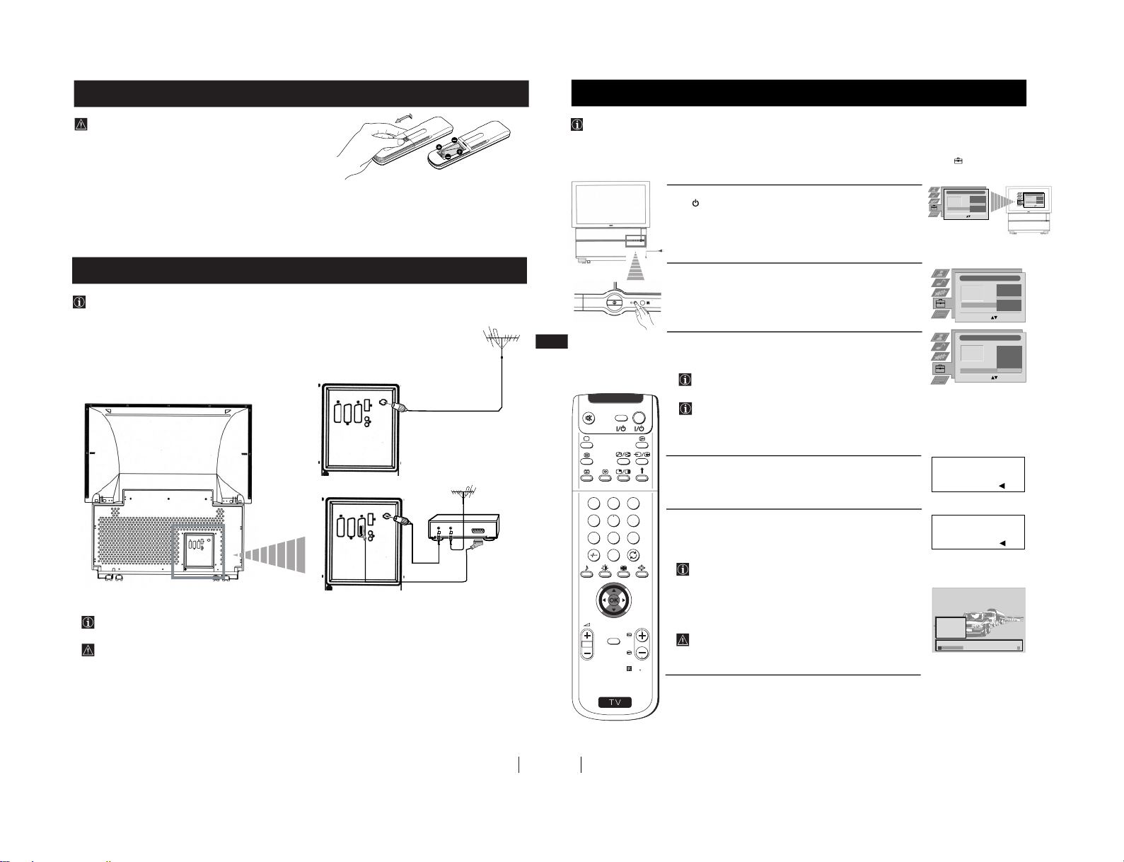
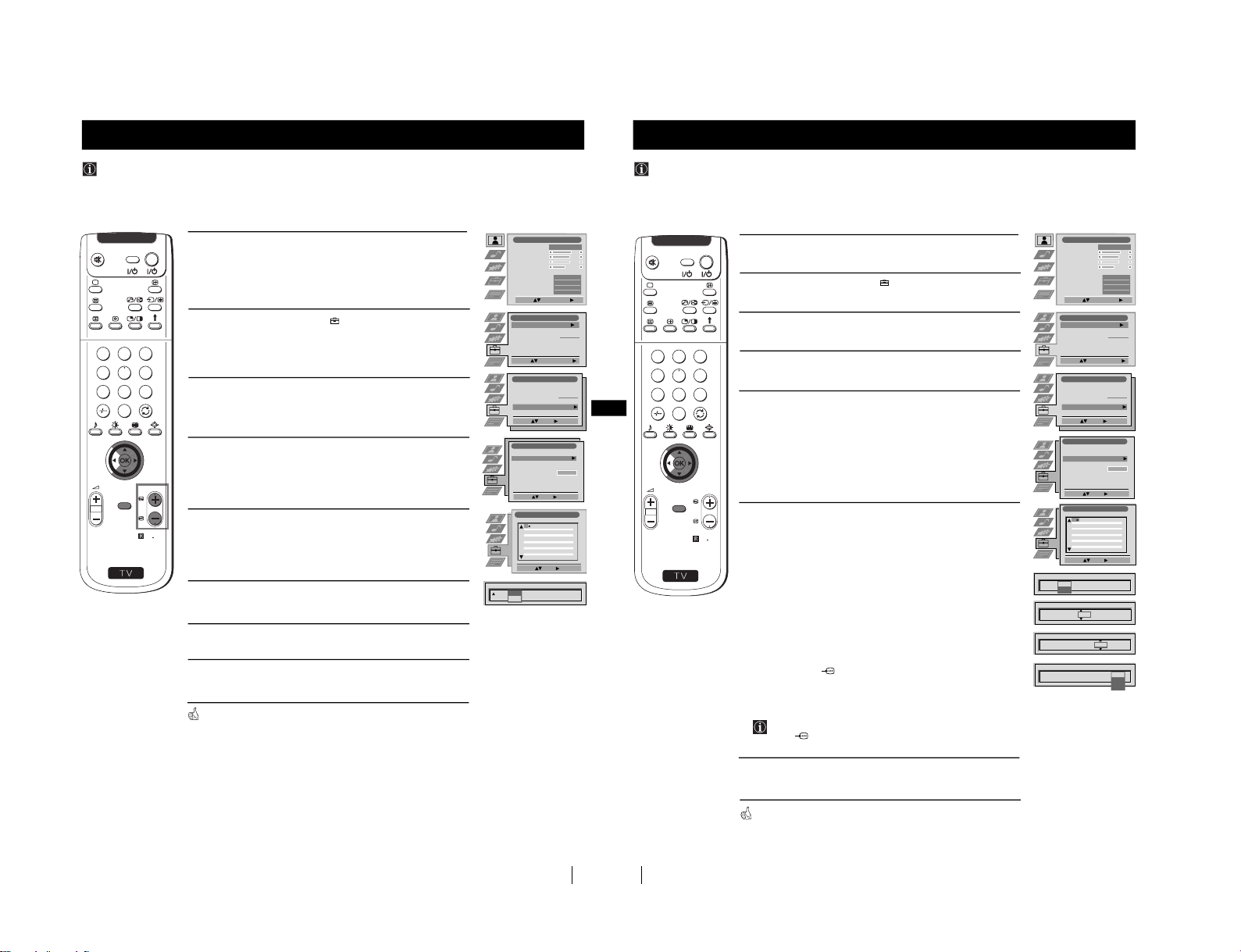
Installation
Make sure you insert the batteries using the correct
polarities.
Always remember to dispose of used batteries in an
environmental friendly way.
Inserting Batteries into the Remote Control
Connecting cables are not supplied.
Connecting the Aerial and VCR
or
VCR
The Scart lead is optional.
If you use this optional connection it can improve picture and sound quality when using a VCR.
If you do not use a SCART lead, after automatically tuning the projection TV refer to the "Manually Tuning the TV"
section of this instruction manual, to tune in the set to the output of your VCR. Also refer to your VCR instruction manual
to find out how to find the output channel of your VCR.
OUT
IN
Installation
– 8 –
Page 9
9
GB
First Time Operation
S
RM
903
PROGR
MENU
1
4
7
2
5
8
0
3
6
9
V
I
DETV
O
Programme Sorting
Select Prog: Confirm:
PROG CH LABEL
1
2
3
4
5
6
7
8
9
10
11
C03
C05
C07
C08
C09
C11
C12
C13
C14
C15
C16
TV 5
PRO 7
EU-SP
SWF
RTL
SAT
MDR
DDI
DSF
RTL 2
KAB 1
Programme Sorting
Select Position: Move: OK
C03 TV 5
PROG CH LABEL
C03
C05
C07
C08
C09
C11
C12
C13
C14
C15
C16
TV 5
PRO 7
EU-SP
SWF
RTL
SAT
MDR
DDI
DSF
RTL 2
KAB 1
1
2
3
4
5
6
7
8
9
10
11
6
After all available channels are captured and stored, the
Programme Sorting menu appears automatically on the screen
enabling you to change the order in which the channels appear
on the screen.
a) If you do not wish to change the channel order, go to step 7.
b) If you wish to change the channel order:
1Push the joystick on the remote control $ or 4 to select the
programme number with the channel (TV Broadcast) you wish to
rearrange, then push z to enter.
2 Push the joystick $ or 4 to select the new programme number
position for your selected channel (TV Broadcast), then press OK.
The selected channel now moves to its new programme
position and the other channels move accordingly.
3Repeat steps b1) and b2) if you wish to change the order of the
other channels.
7
Press the MENU button to exit and return to the normal TV screen.
The set is now ready for use.
First Time Operation
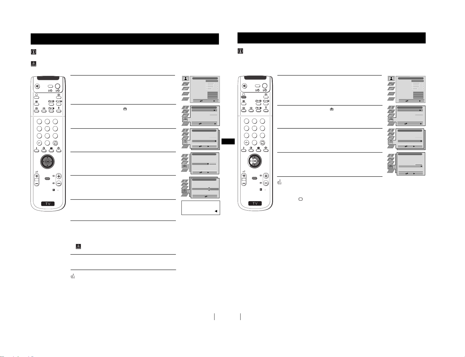
Due to the earth’s magnetism, the picture might become undefined and you could see different colours on the outlines of the images.
In that case, proceed as follows.
Adjusting Colour Registration (Convergence)
Auto converge the Red, Green, and
Blue Lines
1
Press on the mark , on the front of the projection TV to reveal the
front connectors.
2
Press button.
The Auto Convergence function works for about 10 seconds. When the white
cross disappears from the screen, your projection TV is ready for use.
Notes:
The Auto Convergence function does not work when:
• no signal is input.
• the input signal is weak.
• the screen is exposed to spotlights or direct sunlight.
• you watch the teletext broadcast.
• you watch NexTView.
10
GB
1
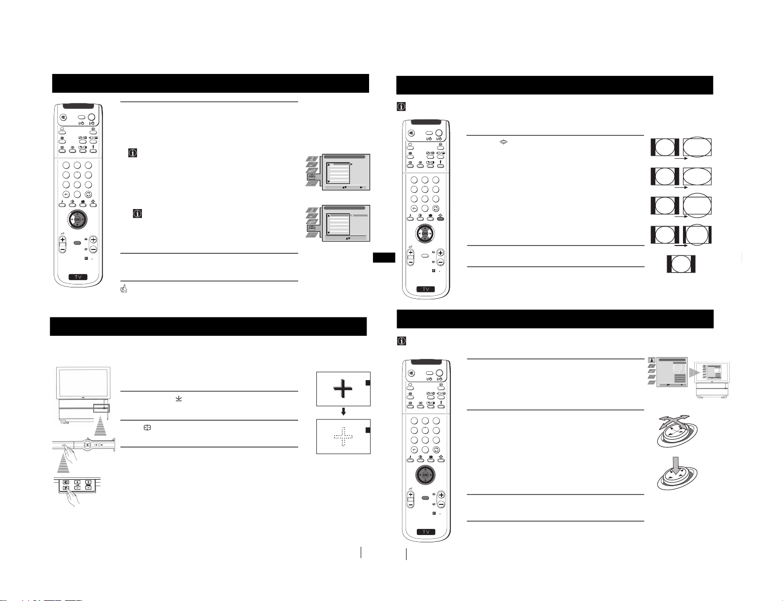
Press the button on the remote control repeatedly to select one
of the following formats.
Smart: imitation of wide screen effect for 4:3 broadcast.
4:3: conventional 4:3 picture size, full picture information.
14:9: compromise between 4:3 and 16:9 picture size.
Zoom: widescreen format for letterbox movies.
Wide: for 16:9 broadcast.
In Smart, Zoom and 14:9 modes parts of the top and bottom of the
screen are cut off. Press $ or 4 to adjust the position of the image on
screen (eg to read subtitles).
2
Press the OK button to confirm your selection.
Menu System
This feature allows you to change the size of the TV picture.
Changing the Screen Format
1
Press the MENU button to switch the first level menu on.
2
•To higlight the desired menu or option, push the joystick
4 or $.
•To enter to the selected menu or option, push z
•To return to the last menu or option, push Z.
•To alter settings of your selected option, push $/4/Z or z.
•To confirm and store your selection, press OK.
3
Press the MENU button to remove the menu from the screen.
Your set uses an on-screen menu system to guide you through the operations. Use the following buttons on the
Remote Control to operate the menu system:
Introducing the Menu system
OK
push
$/4/Z or z
press OK
Picture Adjustment
Select: Enter Menu:
Picture Mode
Contrast
Brightness
Colour
Sharpness
Reset
AI
Noise Detection
Digital Mode
Colour Tone
Personal
On
On
DRC 50
Normal
Picture Adjustment
Select: Enter Menu:
Picture Mode
Contrast
Brightness
Colour
Sharpness
Reset
AI
Noise Detection
Digital Mode
Colour Tone
Personal
On
On
DRC 50
Normal
S
RM
903
PROGR
MENU
1
4
7
2
5
8
0
3
6
9
TV
V
I
D
E
O
Joystick:
S
RM
903
PROGR
MENU
1
4
7
2
5
8
0
3
6
9
TV
V
I
D
E
O
4:3
14:9
Zoom
Wide
Smart
10
Menu System
– 9 –
Page 10
11
GB
1
Press the MENU button on the remote control to display the menu
on the screen.
2
Push the joystick z to enter the Picture Adjustment menu.
3
Push the joystick $ or 4 to select the item you wish to change,
then push z to enter.
Refer to the table below to chose the item and for the effect of
each control:
Picture Mode $ Live (for live broadcast programmes)
Personal (for individual settings)
Movie (for films)
4 Game (for computer games)
Contrast Z Less z More
Brightness
*
Z Darker z Brighter
Colour
*
Z Less z More
Sharpness
*
Z Softer z Sharper
Hue
**
Z Reddish z Greenish
Reset Resets picture to the factory preset levels.
AI (Artificial 4 Off: Normal
Intelligence) $ On: Automatic optimization of contrast level
according to the TV signal
Noise 4 Off: Normal
Detection $ On: Reduces picture noise in the case of a
weak/noisy broadcast signal.
Digital Mode $ DRC 50: improves picture resolution and is optimal
for viewing scrolling characters.
4 DRC 100: improves picture resolution creating
flicker-free pictures.
Colour Tone $ Warm: Gives a warm tint to the picture.
---Normal: Normal.
4 Cool: Gives a cool tint to the picture.
*
Can only be altered if Personal Picture Mode is selected.
**
Only avalaible for NTSC colour signal (e.g: USA video tapes).
4
Push the joystick 4, $, Z or z to alter the selected item, then
press the OK button to store the new adjustment.
5
Repeat steps 3 and 4 to alter the other items.
6
Press the MENU button to exit and return to the normal TV screen.
Changing the Picture Mode Quickly
You can quickly change the Picture Mode without entering the
Picture Control menu screen.
1
Press the button on the remote control repeatedly to directly
access and select your desired picture mode (Live, Personal, Movie,
or Game).
2
Press the OK button to remove the display from the screen.
Menu System
Although the picture is adjusted at the factory, you can modify it to suit your own taste.
Adjusting the Picture
Picture Adjustment
Select: Enter Menu:
Picture Mode
Contrast
Brightness
Colour
Sharpness
Reset
AI
Noise Detection
Digital Mode
Colour Tone
Personal
On
On
DRC 50
Normal
Picture Mode
Live
Personal
Movie
Game
Contrast
AI
On
Off
Picture Mode
Live
Personal
Movie
Game
Colour Tone
Warm
Normal
Cool
Picture Adjustment
Select: Enter:
Picture Mode
Contrast
Brightness
Colour
Sharpness
Reset
AI
Noise Detection
Digital Mode
Colour Tone
Personal
On
On
DRC 50
Normal
Digital Mode
DRC 50
DRC 100
Noise Detection
On
Off
S
RM
903
PROGR
MENU
1
4
7
2
5
8
0
3
6
9
TV
V
I
D
E
O
K
Menu System
12
Menu System
Menu System
Although the sound is adjusted at the factory, you can modify it to suit your own taste.
Adjusting the Sound
1
Press the MENU button on the remote control to display the menu
on the screen.
2
Push the joystick $ to select the symbol, then push z to enter to the
Audio Adjustment menu.
3
Push the joystick $ or 4 to select the item you wish to change,
then push z to enter.
Refer to the table below to chose the item and for the effect of
each control:
Equaliser Mode $ Personal (for individual settings)
Vocal
Jazz
Rock
Pop
4 Flat (fixed setting, cannot be adjusted)
*Equaliser Push to
z
or
Z
to select the frequency band you
Adjustment want to alter and push to
$
or
4
to adjust. Finally,
press the OK button to store the new adjustment.
Balance Z Left z Right
Loudness $ Off: normal
4 On: for music broadcasts
Space $ Off: normal
4 On: acoustic sound effect
Auto Vol. $ Off: volume level changes according to the
Control broadcast signal
4 On: volume level of the channels will stay the same
independent of the broadcast signal (e.g. in
case of advertisement)
Dual Sound • For a stereo broadcast:
$ Mono
4 Stereo
• For a bilingual broadcast:
$ Mono (for mono channel if available)
A (for channel 1)
4 B (for channel 2)
Headphones:
l
Volume Z Less z More
l
Dual Sound • For a stereo broadcast:
$ Mono
4 Stereo
• For a bilingual broadcast:
$ Mono (for mono channel if available)
A (for channel 1)
B (for channel 2)
4 PAP (only when PAP is switched on)
*
Can only be permanently stored if Personal Equaliser Mode is selected,
the other modes (Vocal, Jazz, Rock or Pop) store until the next mode
change.
S
RM
903
PROGR
MENU
1
4
7
2
5
8
0
3
6
9
TV
V
I
D
E
O
Picture Adjustment
Select: Enter Menu:
Picture Mode
Contrast
Brightness
Colour
Sharpness
Reset
AI
Noise Detection
Digital Mode
Colour Tone
Personal
On
On
DRC 50
Normal
Audio Adjustment
Equaliser Mode
Equaliser
Adjustment
Balance
Loudness
Space
Auto Vol. Control
Dual Sound
Volume
Dual Sound
Personal
Mono
Off
Off
Off
Mono
Select: Enter:
0
.
0
0
Audio Adjustment
Equaliser Mode
Equaliser
Adjustment
Balance
Loudness
Space
Auto Vol. Control
Dual Sound
Volume
Dual Sound
Personal
Mono
Off
Off
Off
Mono
Personal
Vocal
Jazz
Rock
Pop
Flat
Select Mode: Confirm: OK
0
.
0
0
Equaliser Adjustment
Sel: Adjust: Confirm:OK
(Personal)
+
0
–
120 500 1,5K 5 K 10 K
Balance
.
Loudness
Off
On
Space
Off
On
Auto Vol. Control
Off
On
Dual Sound
Mono
A
B
Volume
Dual Sound
B
A
continued...
– 10 –
Page 11
13
GB
Menu System
4
Push the joystick $, 4, Z or z to alter the selected item, then
press the OK button to store the new adjustment.
5
Repeat steps 3 and 4 to alter the other items.
6
Press the MENU button to exit and return to the normal TV screen.
Changing Sound Mode Quickly
You can quickly change Sound mode without entering the Sound
Control menu screen.
1
Press the button on the remote control repeatedly to directly
access and select your desired sound mode (Personal, Vocal, Jazz,
Rock, Pop or Flat).
2
Press the OK button to remove the display from the screen.
Menu System
Equaliser Mode
Personal
Vocal
Jazz
Rock
Pop
Flat
S
RM
903
PROGR
MENU
1
4
7
2
5
8
0
3
6
9
TV
V
I
D
E
O
14
Menu System
Menu System
Using the Features menu you can:
a) Select if you want to listen to the sound from the set directly or through an external amplifier.
b) Adjust automatically the size of picture.
c) Select a time period after which the set switches itself into standby mode.
d)
Lock the buttons on the set. In this way, the set only works by using the remote control buttons.
e) Select the source to be output from the Scart connector :2/q2 (SMARTLINK). In this way you can record from this scart
connector while watching another source. If your VCR supports Smartlink, this procedure is not necessary.
Using the Features Menu
1
Press the MENU button on the remote control to display the menu
on the screen.
2
Push the joystick $ to select the symbol, then push z to enter to
the Features menu.
3
Push the joystick $ or 4 to select the desired menu item, then
push z to enter (see the table below for the effect of each menu item).
4
Push $ or 4 to select the desired setting and press the OK button
to store.
5
Press the MENU button to exit and return to the normal TV screen.
Features Effect / Operation
Speaker $ Main (sound from the set)
4 Centre In (sound from external amplifier)
Auto Format $ Off: Size of picture is not automatically adjusted.
(only for aerial Normal: Size of picture is automatically adjusted
signal) according to the broadcaster information.
4 Full: The set automatically adjusts the picture size
to eliminate any dark areas on the TV picture (as
shown on the section
“Changing the Screen
Format)”.
Format Correction
$ Off: 4:3/14:9 is selected.
(only if Auto Format
is set to “Normal”
4 On: Smart mode is selected automatically for
or “Full”)
4:3/14:9 broadcast.
Sleep Timer
4 Off
10 min.
20 min.
...
$ 90 min.
• One minute before the set switches into standby
mode, the time remaining is displayed on the
screen automatically.
• When watching the TV, press the
button on
the remote control to display the time remaining.
• To return to normal operation from standby
mode, press the TV
button on the remote
control.
Parental lock $ Off (Normal mode)
4 On (The set can only be switched on using the
remote control, the buttons on the TV do not
work)
AV2 Output $ TV (audio/video signal from the aerial)
AV1
(audio/video signal from the Scart
connector :1/
).
AV2 (audio/video signal from the Scart
connector
:
2/q2 (SMARTLINK).
AV3 (audio/video signal from the Scart
connector
:
3/q3).
4 AV4 (audio/video signal from the connector … 4
placed in the front of the set).
If you have connected a decoder, please remember
to change back the AV2 Output to "TV" for correct
unscrambling.
Picture Adjustment
Select: Enter Menu:
Picture Mode
Contrast
Brightness
Colour
Sharpness
Reset
AI
Noise Detection
Digital Mode
Colour Tone
Personal
On
On
DRC 50
Normal
Features
Auto Format
Format Correction
Sleep Timer
Parental Lock
AV2 Output
Normal
On
Off
Off
TV
Select: Enter:
Speaker
Main
Speaker
Main
Centre In
10 min
Sleep Timer
Parental Lock
Off
On
AV2 Output
TV
AV1
AV2
AV3
AV4
Auto Format
Off
Normal
Full
Format Correction
Off
On
S
RM
903
PROGR
MENU
1
4
7
2
5
8
0
3
6
9
TV
V
I
D
E
O
– 11 –
Page 12
15
GB
1
Press the MENU button on the remote control to display the
menu on the screen.
2
Push the joystick $ to select the symbol, then push z to enter
the Set Up menu.
3
Push the joystick $ or 4 to select Manual Set Up, then push
z to enter.
4
Push the joystick $ or 4 to select Manual Programme Preset,
then push z to enter.
5
Push the joystick $ or 4 to select on which programme number
you want to preset a channel (for VCR select programme number
"0"), then push twice z. The column SYS is highlighted.
6
Push the joystick $ or 4 to select the system for TV Broadcast
and VCR channel (B/G for western european countries, L for
France, I for Great Britain or D/K for eastern european countries)
or a external input source (EXT), then push z. The column CH
is highlighted.
7
Push the joystick $ or 4 to select the channel tuning, "C" for
terrestrial channels (for TV Broadcast or VCR channel), "S" for
cable channels or F for, direct frequency input then push z.
8
a) If you know the channel number of the TV Broadcast, the VCR
test signal channel or the frequency, press the number buttons
to enter directly the channel number. Then press the OK button
to store.
b) If you do not know the channel number, push the joystyck $
to select SEARCH and the set starts automatically to search for
the next available TV Broadcast channel or the channel of the
VCR signal. Then press the OK button to store or push $ to
continue searching the desired channel.
c) For external input sources (EXT), push $ to select the input
source where you have connected your equipment (AV1, AV2,
AV3 or AV4). Then press the OK button to store.
9
Repeat steps 4 to 8 a), b) or c) if you wish to store more channels.
10
Press the MENU button to exit and return to the normal TV screen.
The set is now ready for use.
Menu System
Picture Adjustment
Select: Enter Menu:
Picture Mode
Contrast
Brightness
Colour
Sharpness
Reset
AI
Noise Detection
Digital Mode
Colour Tone
Personal
On
On
DRC 50
Normal
Set Up
Auto Tuning
Programme Sorting
Select NexTView
AV Preset
Manual Set Up
Select:
Start Auto Tuning
Start
- - - - - - -
Enter:
Set Up
Auto Tuning
Programme Sorting
Select NexTView
AV Preset
Manual Set Up
Select:
- - - - - - -
Manual Set Up
Select: Enter :
Language/Country
Manual Programme Preset
Further Programme Preset
RGB Set Up
Personal ID
Demo
- - - - - - -
Manual Programme Preset
Select: Enter :
PROG CHSYSSKIP LABEL
C09
C10
ARD
BBC
B/G
B/G
Off
Off
Off
Off
Off
Off
Off
Off
Off
Off
Off
1
2
3
4
5
6
7
8
9
10
11
PROG CHSYS
Off
SKIP LABEL
1
B/G
L
I
D/K
EXT
PROG SYS
Off
SKIP LABEL
1 B/G
CH
C
S
F
- -
PROG SYS
Off
SKIP LABEL
1 B/G
CH
03
SEARCH
C
PROG CHSYS
Off
SKIP LABEL
3 EXT
AV1
AV2
AV3
AV4
S
RM
903
PROGR
MENU
1
4
7
2
5
8
0
3
6
9
TV
V
I
D
E
O
Menu System
Use this function to preset channels (TV Broadcast) or a video input source one by one to the programme order of your choice.
Manually Tuning the TV
16
Menu System
Menu System
Names for channels (TV Broadcasts) are usually taken automatically from Teletext if available. You can however name a channel or
an input video source using up to five characters (letters or numbers). Using this function, you can easily identify which channel
(TV Broadcasts) or video source you are watching.
Labelling a channel
1
Press the MENU button on the remote control to display the
menu on the screen.
2
Push the joystick $ to select the symbol, then push z to enter
the Set Up menu.
3
Push the joystick $ or 4 to select Manual Set Up, then push
z to enter.
4
Push the joystick $ or 4 to select Manual Programme Preset,
then push z to enter.
5
Push the joystick $ or 4 to select the programme number with
the channel you wish to name.
6
Push the joystick z repeatedly until the first element of the
LABEL column is highlighted.
7
Push the joystick $ or 4 to select a letter, number, "+" or a
blank, then push z to confirm this character. Select the other
four characters in the same way.
8
After selecting all the characters, press the OK button.
9
Repeat steps 5 to 8 if you wish to label other channels.
10
P
ress the MENU button to exit and return to the normal TV
screen.
When you select a named channel, the name appears for a few seconds
on the screen.
S
RM
903
PROGR
MENU
1
4
7
2
5
8
0
3
6
9
TV
V
I
D
E
O
Picture Adjustment
Select: Enter Menu:
Picture Mode
Contrast
Brightness
Colour
Sharpness
Reset
AI
Noise Detection
Digital Mode
Colour Tone
Personal
On
On
DRC 50
Normal
Set Up
Auto Tuning
Programme Sorting
Select NexTView
AV Preset
Manual Set Up
Select:
Start Auto Tuning
Start
- - - - - - -
Enter:
Set Up
Auto Tuning
Programme Sorting
Select NexTView
AV Preset
Manual Set Up
Select:
- - - - - - -
Manual Set Up
Select: Enter :
Language/Country
Manual Programme Preset
Further Programme Preset
RGB Set Up
Personal ID
Demo
- - - - - - -
Manual Programme Preset
Select: Enter:
PROG CHSYSSKIP LABEL
C09
C10
ARD
BBC
B/G
B/G
Off
Off
Off
Off
Off
Off
Off
Off
Off
Off
Off
1
2
3
4
5
6
7
8
9
10
11
PROG SYS
Off
SKIP LABEL
1 B/G
CH
C 03
A
– 12 –
Page 13
17
GB
1
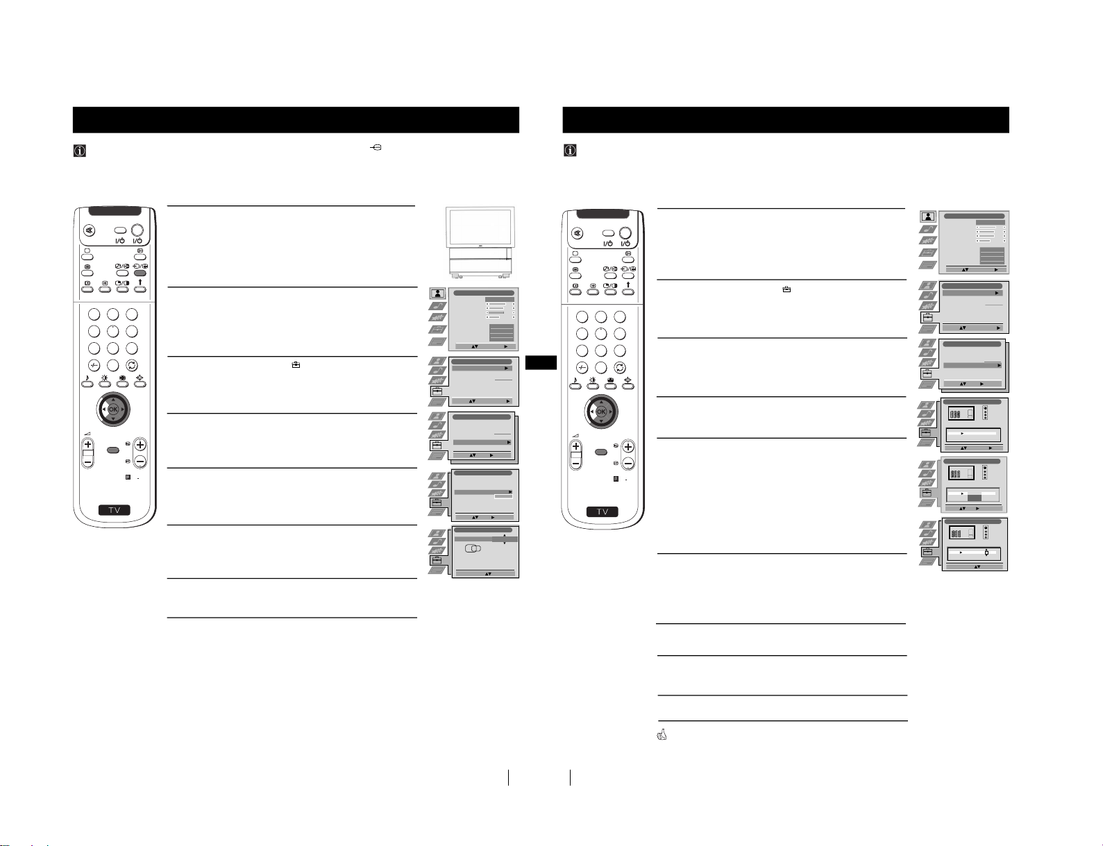
Press the MENU button on the remote control to display the menu
on the screen.
2
Push the joystick $ to select the symbol, then push z to enter
the Set Up menu.
3
Push the joystick $ or 4 to select Manual Set Up, then push z to
enter.
4
Push the joystick $ or 4 to select Manual Programme Preset,
then push z to enter.
5
Push the joystick $ or 4 to select the programme position you
want to skip, then push z to enter the SKIP column.
6
Push the joystick $ to select On, then press the OK button to
store.
7
Repeat steps 5 and 6 to skip other unused programme positions.
8
Press the MENU button to exit and return to the normal TV screen.
When changing channels (TV Broadcasts) with the PROGR +/- buttons,
the skipped programme positions do not appear. You can, however, still
select them using the number buttons.
Menu System
Menu System
You can programme this set to skip any unwanted programme numbers when they are selected with the PROGR +/buttons. To cancel this function afterwards, proceed in the same way as described below by selecting Off instead of On in step 6.
Skipping Programme positions
S
RM
903
PROGR
MENU
1
4
7
2
5
8
0
3
6
9
TV
V
I
D
E
O
Picture Adjustment
Select: Enter Menu:
Picture Mode
Contrast
Brightness
Colour
Sharpness
Reset
AI
Noise Detection
Digital Mode
Colour Tone
Personal
On
On
DRC 50
Normal
Set Up
Auto Tuning
Programme Sorting
Select NexTView
AV Preset
Manual Set Up
Select:
Start Auto Tuning
Start
- - - - - - -
Enter:
Set Up
Auto Tuning
Programme Sorting
Select NexTView
AV Preset
Manual Set Up
Select:
- - - - - - -
Manual Set Up
Select: Enter:
Language/Country
Manual Programme Preset
Further Programme Preset
RGB Set Up
Personal ID
Demo
- - - - - - -
PROG SYSSKIP LABEL
1 B/G
CH
C 09
ARD
Off
On
Manual Programme Preset
Select: Enter:
PROG CHSYSSKIP LABEL
C09
C10
ARD
BBC
B/G
B/G
Off
Off
Off
Off
Off
Off
Off
Off
Off
Off
Off
1
2
3
4
5
6
7
8
9
10
11
18
Menu System
Menu System
With this feature you can:
a) Individually attenuate the strength of a channel signal in case of a strong local aerial signal (striped picture).
b) Individually adjust the volume level of each channel.
c) Normally the automatic fine tuning (AFT) is operating, however you can manually fine-tune the TV to obtain better
reception if the picture is distorted.
d) Preset the AV output for the programme positions of channels with scrambled signals (eg from a pay TV decoder). In this way
a connected VCR records the unscrambled signal.
Using the "Further Programme Preset" function
1
Press the MENU button on the remote control to display the menu
on the screen.
2
Push the joystick $ to select the symbol, then push z to enter
the Set Up menu.
3
Push the joystick $ or 4 to select Manual Set Up then push to z
to enter.
4
Push the joystick $ or 4 to select Further Programme Preset,
then push z to enter.
5
Push the joystick $ or 4 to select the relevant programme number,
then push z repeatedly to select:
a) ATT (RF attenuator)
b) VOL (Volume Offset)
c) AFT (Automatic Fine Tuning) or
d) DECODER
The selected item changes colour.
6
a) ATT
Push the joystick $ to select On, then press the OK button.
Repeat steps 5 and 6 a) to attenuate other channels.
b) VOL
Push the joystick $ or 4 to adjust the volume level of the channel
over a range of -7 to +7, then press the OK button. Repeat steps 5
and 6b) to adjust the volume level of the other channels.
c) AFT
Push the joystick $ or 4 to fine tune the channel frequency over
a range of -15 to +15, then press the OK button. Repeat steps 5 and
6c) if you wish to fine tune other channels.
d) DECODER
Push the joystick $ or 4 to select AV1 (for a decoder connected
to the Scart :1/ ) or AV2 (for a decoder connected to the Scart
:2/q 2 (SMARTLINK)), then press the OK button.
Repeat steps 5 and 6d) to select the AV1 or AV2 output for other
programme positions.
The picture from the decoder connected to the Scart connector
:1/ or :2/q 2 (SMARTLINK) on the back of the
set will appear on this programme number.
7
Press the MENU button to exit and return to the normal TV screen.
The set is now ready for use.
S
RM
903
PROGR
MENU
1
4
7
2
5
8
0
3
6
9
TV
V
I
D
E
O
Picture Adjustment
Select: Enter Menu:
Picture Mode
Contrast
Brightness
Colour
Sharpness
Reset
AI
Noise Detection
Digital Mode
Colour Tone
Personal
On
On
DRC 50
Normal
Set Up
Auto Tuning
Programme Sorting
Select NexTView
AV Preset
Manual Set Up
Select:
Start Auto Tuning
Start
- - - - - - -
Enter:
Set Up
Auto Tuning
Programme Sorting
Select NexTView
AV Preset
Manual Set Up
Select:
- - - - - - -
Manual Set Up
Select: Enter :
Language/Country
Manual Programme Preset
Further Programme Preset
RGB Set Up
Personal ID
Demo
- - - - - - -
Further Programme Preset
Select: Enter:
PROG AFTVO LATT DECODER
On
On
On
Off
Off
Off
0
0
0
Off
Off
Off
1
2
3
4
5
6
7
8
9
10
11
PROG AFTVOLATT DECODER
1
Off
On
PROG AFTVOLATT DECODER
1 On -5
2
PROG AFTVO LATT DECODER
1 On -5 2
Off
AV1
AV2
PROG AFTVOLATT DECODER
1On
- 5
– 13 –
Page 14
19
GB
1
Press the MENU button on the remote control to display the menu
on the screen.
2
Push the joystick $ to select the symbol, then push z to
enter the Set Up menu.
3
Push the joystick $ or 4 to select Manual Set Up, then push z to
enter.
4
Push $ or 4 to select Personal ID, then push z to enter.
5
Push the joystick $ or 4 to select a letter, number, + or a blank;
then push z to confirm this character. Select the other ten
characters in the same way.
6
After selecting all the characters, press the OK button. A new menu
appears automatically on the screen asking you to be sure that you
want to save this ID.
7
a) If you do not wish to store this ID, push the joystick Z and
repeat steps 4 to 6 to enter a new ID.
b) If you wish to store this ID, press the OK button.
Remember that this code can only be input once.
8
Press the MENU button to return to the normal TV screen.
When you enter the Manual Set Up menu, in the "Personal ID" option the
code you entered above will be displayed. You will not be able to select and
change this option.
Menu System
Menu System
You can programme this set with a personal code, using up to eleven characters (letters and numbers). Then using
this fuction it will be possible to identify your set if it was ever stolen.
This code can only be input once!
Make sure to write it down in this instruction manual.
Inputting Your Personal ID
S
RM
903
PROGR
MENU
1
4
7
2
5
8
0
3
6
9
TV
V
I
D
E
O
Picture Adjustment
Select: Enter Menu:
Picture Mode
Contrast
Brightness
Colour
Sharpness
Reset
AI
Noise Detection
Digital Mode
Colour Tone
Personal
On
On
DRC 50
Normal
Set Up
Auto Tuning
Programme Sorting
Select NexTView
AV Preset
Manual Set Up
Select:
Start Auto Tuning
Start
- - - - - - -
Enter:
Set Up
Auto Tuning
Programme Sorting
Select NexTView
AV Preset
Manual Set Up
Select:
- - - - - - -
Manual Set Up
Select: Enter:
Language/Country
Manual Programme Preset
Further Programme Preset
RGB Set Up
Personal ID
Demo
- - - - - - -
Manual Set Up
Select A-Z, 0-9: Store: OK
Language/Country
Manual Programme Preset
Further Programme Preset
RGB Set Up
Personal ID
Demo
A----------
Are you sure?
Save: OK Cancel:
20
Menu System
This function provides an overview of some of the features available on this set.
Using the Demo Mode
Menu System
1
Press the MENU button on the remote control to display the menu
on the screen.
2
Push the joystick $ to select the symbol, then push z to
enter the Set Up menu.
3
Push the joystick $ or 4 to select Manual Set Up, then push to z to
enter.
4
Push $ or 4 to select Demo, then push z to enter and start
the demonstration.
The set starts the demonstration and shows most of the
available picture functions.
Note:
Press the button on the remote control to stop the Demo mode
and return to the normal TV screen.
S
RM
903
PROGR
MENU
1
4
7
2
5
8
0
3
6
9
TV
V
I
D
E
O
Picture Adjustment
Select: Enter Menu:
Picture Mode
Contrast
Brightness
Colour
Sharpness
Reset
AI
Noise Detection
Digital Mode
Colour Tone
Personal
On
On
DRC 50
Normal
Set Up
Auto Tuning
Programme Sorting
Select NexTView
AV Preset
Manual Set Up
Select:
Start Auto Tuning
Start
- - - - - - -
Enter:
Set Up
Auto Tuning
Programme Sorting
Select NexTView
AV Preset
Manual Set Up
Select:
- - - - - - -
Manual Set Up
Select: Enter :
Language/Country
Manual Programme Preset
Further Programme Preset
RGB Set Up
Personal ID
Demo Start
- - - - - - -
– 14 –
Page 15
21
GB
1
Press the … button repeatedly on the remote control until the
symbol …1 appears on the screen.
2
Push the MENU button to display the menu on the screen.
3
Push the joystick $ to select the symbol, then push z to enter the
Set Up menu.
4
Push $ or 4 to select Manual Set Up then push z to enter.
5
Push the joystick $ or 4 to select RGB Set Up then push z to enter.
6
Push the joystick z to enter H Centre, then push $ or 4 to
adjust the centre of the picture over a range of -10 to +10. Press
the OK button to store.
7
Press the MENU button to exit and return to the normal TV screen.
Menu System
S
RM
903
PROGR
MENU
1
4
7
2
5
8
0
3
6
9
TV
V
I
D
E
O
Menu System
When connecting an RGB source, such as a DVD player, to the Scart connector :1/ you may need to readjust the H Centre
of the picture.
Adjusting the H Centre picture for an RGB source
Picture Adjustment
Select: Enter Menu:
Picture Mode
Contrast
Brightness
Colour
Sharpness
Reset
AI
Noise Detection
Digital Mode
Colour Tone
Personal
On
On
DRC 50
Normal
Set Up
Auto Tuning
Programme Sorting
Select NexTView
AV Preset
Manual Set Up
Select:
Start Auto Tuning
Start
- - - - - - -
Enter:
Set Up
Auto Tuning
Programme Sorting
Select NexTView
AV Preset
Manual Set Up
Select:
- - - - - - -
Manual Set Up
Select: Enter:
Language/Country
Manual Programme Preset
Further Programme Preset
RGB Set Up
Personal ID
Demo
- - - - - - -
RGB Set Up
RGB Set Up
Adjust Position: Confirm: OK
H Centre
O
… 1
22
Menu System
Menu System
This function enables you to select the size of the picture coming from the input source as well as designate a name to the optional
equipment you have connected to the sockets of this set. This name can contain up to 5 characters (letters or numbers).
Labelling and Selecting the screen format of Input Sources
1
Press the MENU button on the remote control to display the menu
on the screen.
2
Push the joystick $ to select the symbol, then push z to
enter the Set Up menu.
3
Push the joystick $ or 4 to select AV Preset, then push z to enter.
4
Push the joystick $ or 4 to select the input source. Then push z to
enter.
5
Push the joystick $ or 4 to select:
$ Off (size of picture is not automatically adjusted).
Normal (size of picture is automatically adjusted according to the
broadcaster information).
4 Full (The set automatically adjusts the picture size to eliminate
any dark areas on the TV picture (as shown on the section
“Changing the Screen Format”).
Next push z .
6
With the first element of the LABEL column highlighted, push the
joystick $ or 4 to select a letter, number, "+" or blank;
then push z to confirm this character. Select the other four
characters in the same way.
7
After selecting all the characters, press the OK button.
8
Repeat steps 4 to 7 if you wish to select the picture size or label other
input sources.
9
Press the MENU button to exit and return to the normal TV screen.
Whenever the equipment with the labelled input is selected for use, the name
appears for a few seconds on the screen
S
RM
903
PROGR
MENU
1
4
7
2
5
8
0
3
6
9
TV
V
I
D
E
O
Picture Adjustment
Select: Enter Menu:
Picture Mode
Contrast
Brightness
Colour
Sharpness
Reset
AI
Noise Detection
Digital Mode
Colour Tone
Personal
On
On
DRC 50
Normal
Set Up
Auto Tuning
Programme Sorting
Select NexTView
AV Preset
Manual Set Up
Select:
Start Auto Tuning
Start
- - - - - - -
Enter:
Set Up
Auto Tuning
Programme Sorting
Select NexTView
AV Preset
Manual Set Up
Select:
- - - - - - -
AV Preset
Select: Enter:
INPUT LABEL
VIDEO
VIDEO
VIDEO
AV1
AV2
AV3
AV4
AUTO FORMAT
Off
Off
Normal
Full
AV Preset
Select A-Z, 0-9: Confirm: OK
INPUT LABEL
IDEO
V
VIDEO
VIDEO
AV1
AV2
AV3
AV4
AUTO FORMAT
Off
Off
Normal
Normal
AV Preset
Select: Next: Confirm: OK
INPUT LABEL
VIDEO
VIDEO
VIDEO
AV1
AV2
AV3
AV4
AUTO FORMAT
Off
Off
Normal
Full
– 15 –
Page 16
23
GB
1
Press the button on the remote control to select the PIP mode.
Now 13 programme positions appear on the screen, with the current
channel in the centre.
2
Push the joystick $, 4, Z or z to move within the 13 displayed
channels.
3
Press the OK button to select the framed channel. The selected
channel moves to the centre.
4
Press to return to the normal TV mode.
Menu System
Menu System
Multi PIP (Picture in Picture) mode displays a succession of 12 still pictures and a 13th that is live. You can manually select which
channel you wish to watch, either full-screen or in the PIP.
Using Multi PIP (Picture In Picture)
S
RM
903
PROGR
MENU
1
4
7
2
5
8
0
3
6
9
TV
V
I
D
E
O
03 05
01 06
11 09 08
02
10
07
13
12
04
Switching PAP on and off
Press the button / on the remote control to display the two screens
in format 4:3. Press / again to switch PAP off.
Selecting PAP source
1
To change the source of the left screen:
With PAP switched on, press the number buttons (to select a TV
channel) or press … (to select a video source).
2
To change the source of the right screen:
With PAP switched on, press the button on the remote control.
When the symbol appears at the bottom of the right screen,
press the number buttons (to select a TV channel) or press … (to
select a video source).
Swapping screens
With PAP switched on, press the / button on the remote control to
swap the two screens.
Zooming the screens
With PAP switched on, push the joystick repeatedly Z or z to
change the size of the two screens.
Selecting the sound of the right screen
You can select the sound of the right screen via headphones. With
PAP switched on, refer to the "Adjusting the Sound" section of this
instruction manual and set the option "l Dual Sound" to "PAP".
PAP divides the screen into two for watching two channels simultaneously. One of the pictures can be selected to come from a
video source.
The sound of the left screen comes through the set loudspeakers, the sound of the right screen is selectable via
headphones.
Using PAP (Picture And Picture)
S
RM
903
PROGR
MENU
1
4
7
2
5
8
0
3
6
9
TV
V
I
D
E
O
24
Teletext
Teletext
Most TV channels broadcast information via Teletext. The index page of the teletext service (usually page 100) gives you
information on how to use the service.
! Please use a TV channel with a strong signal, otherwise there may be Teletext errors.
Teletext
Switching Teletext on and off
1
Select the TV channel which carries the teletext service you want
to view.
2
Press the button once for Picture and Teletext (P&T). The screen
is divided in two, with the TV channel in the right corner and the
Teletext display on the left.
P&T mode: Press / then press PROGR +/- to change
the channel of the TV screen. Push the joystick Z or z to
change the size of the TV screen then press / again to
resume normal teletext reception.
3
Press twice to get Teletext only.
4
Press three times for Mix mode.
5
Press a fourth time or press to switch off Teletext.
Selecting a Teletext page
Input three digits for the page number using the numbered buttons on
the control. If you make a mistake, type in any three digits then re-enter
the correct page number.
Using Other Teletext Functions
Selecting the next or preceding page
Press the (PROG+) or (PROGR-) buttons on the remote
control to select the previous or next page.
Selecting a sub page
A teletext page may consist of several sub pages. In this case, after a
few seconds, an information line is displayed showing the number of
subpages.
Select the sub page by pressing 4 or $.
To freeze a Teletext page
Press the button to freeze the page. Press again to cancel the freeze.
Revealing the index page
Press the button to reveal the index page (normally page 100).
Fastext
(only available if the TV station broadcasts Fastext signals)
When the colour coded menu appears at the bottom of a teletext page,
press a coloured button on the remote control (red, green, yellow or blue)
to access the corresponding page.
Using the feature "Page Catching"
1
Press the numbered buttons on the remote control to select a teletext
page which has several page numbers on it (eg the index page).
2
Press the OK button.
3
Push the joystick 4 or $ to select the desired page number then
press the OK buttons. The requested page is displayed after
some seconds.
continued...
S
RM
903
PROGR
MENU
1
4
7
2
5
8
0
3
6
9
TV
V
I
D
E
O
TELETEXT
Index
Programme
News
Sport
Weather
25
153
101
98
01
TELETEXT
Index
Programme
News
Sport
Weather
25
153
101
98
TELETEXT
Index
Programme
News
Sport
Weather
25
153
101
98
TELETEXT
Index
Programme
News
Sport
Weather
25
153
101
98
TELETEXT
Index
Programme
News
Sport
Weather
25
153
101
98
TELETEXT
Index
Programme
News
Sport
Weather
25
153
101
98
TELETEXT
Index
Programme
News
Sport
Weather
25
153
101
98
TELETEXT
Index
Programme
News
Sport
Weather
25
153
101
98
TELETEXT
Index
Programme
News
Sport
Weather
25
153
101
98
01
TELETEXT
Index
Programme
News
Sport
Weather
25
153
101
98
216-02
01 03 04 05 06 07 08
02
– 16 –
Page 17
25
GB
Using the Teletext menu
1
With Teletext switched on, press the MENU button on the remote
control to display the teletext menu on the TV screen.
2
Push the joystick 4 or $ to select your chosen item, then push to z
to display the relevant sub menu.
3
To remove the teletext menu from the screen, press the MENU
button.
Top / Bottom / Full
The Top/Bottom/Full sub menu allows you to enlarge different
sections of the Teletext page. Push the joystick 4 to enlarge the
upper half of the screen, push $ to enlarge the lower half. Press
the OK button to restore the page to normal size.
Text Clear
After having selected this function, you can watch a TV channel while
waiting for a requested Teletext page. As soon as the page is available,
the symbol changes colour. To view the page, press .
Reveal
Some teletext pages contain hidden information (eg for a quiz),
which you can reveal. The hidden information appears on screen.
Time Page
(depending on availability of teletext service)
You can call up a time-coded page such as an alarm page at a time
specified by you. After you have displayed the Time Page sub menu:
1
Press the numbered buttons on the remote control to enter the
three digits of the desired page.
2
Press the numbered buttons again to enter the four digits of the
desired time.
3
Press the OK button to store the desired time. The time is displayed
in the top left corner of the screen. At the requested time the page is
displayed.
Page Overview
(depending on availability of teletext service)
In the Page Overview menu the block and group pages of TOP- Text
are sorted into two columns, so that the customer can easily select this
page. For each block page in the first column, the corresponding
group pages are shown in the second column. Push the joystick 4 or $
to select the desired block page, then push z to enter to the group pages
column. Push 4 or $ to select the desired group page .
Finally, press the OK button to display the page.
Teletext
Teletext
S
RM
903
PROGR
MENU
1
4
7
2
5
8
0
3
6
9
TV
V
I
D
E
O
Teletext
Top / Bottom / Full
Text Clear
Reveal
Time Page
Page Overview
Select: Enter:
Top: Bottom: Full: OK
Time Page
PAGE TIME
Select Page: 0-9 Next:
- - : - -
– – –
26
NexTView
NexTView
* (depending on availability of service)
NexTView is an on-screen electronic programme guide (EPG), providing you with programme information for different
broadcasters.
NexTView *
Selecting your NexTView provider
The set automatically selects the best NexTView provider for you.
This provider is available about 30 minutes after the channel tuning.
You can however change this selection of provider if you wish.
1
Press the MENU button on the remote control to display the menu
on the screen.
2
Push the joystick 4 or $ to select the symbol, then push z
to enter the Set Up menu.
3
Push 4 or $ to highlight Select NexTView then push z to enter. A list
is displayed containing all available NexTView providers.
4
Push 4 or $ to select the desired provider then press the OK
button to store.
5
Press the MENU button to remove the menu from the screen.
Displaying NexTView
1
Press the button repeatedly on the remote control to switch
NexTView on and off.
* In some cases, you may also need to push the joystick Z to
display the Sony electronic programme guide.
2
Push the joystick 4, $, Z or z to move the cursor around the screen.
3
Press the OK button to confirm a selection.
a) If you press the OK button in the date, time or icon (themes)
columns, you change the programme list according to the
selection.
b) If you press the OK button in the programme list, you directly
display the channel if the broadcast is currently running, or,
you display the "Long Info" menu if the broadcast is running at
some future time.
Using the "Individual Setting" menu
You can make a personal list of the types of programmes you
wish to view on the programme guide.
1
Push the joystick 4 or $ to select the icon then push to z to
display the "Individual Setting" menu.
2
Push the joystick 4 or $ to select your chosen item on the screen
then press the OK button to confirm your choice.
3
Repeat step 2 for all the items you wish to have in your list.
4
When you have finished the list, push z to select the icon.
5
Press the OK button to return to the previous menu.
6
Push the joystick 4 or $ to select the icon then press the OK
button again to activate your "Individual Setting" filter.
S
RM
903
PROGR
MENU
1
4
7
2
5
8
0
3
6
9
TV
V
I
D
E
O
Picture Adjustment
Select: Enter Menu:
Picture Mode
Contrast
Brightness
Colour
Sharpness
Reset
AI
Noise Detection
Digital Mode
Colour Tone
Personal
On
On
DRC 50
Normal
Set Up
Auto Tuning
Programme Sorting
Select NexTView
AV Preset
Manual Set Up
Select:
Start Auto Tuning
Start
- - - - - - -
7
Tue
07 Tue
12:38
8
Wed
10
Fri
11
Sat
12
Sun
13
Mon
9
Thu
12
SWISS
Star Wars
Super RTL
Hat der alte Hexenmeister sich doch
einmal fortbegeben, und nun sollen
seine Geister auch nach meinem Willen
leben.
Werner - Beinhart
Pro 7
Flui grüsst den Rest der Welt
Kabel 1
Once upon a time in the West
Euronews
International News
RTL Plus
10:35 - 12:45
10:20 - 12:00
10:45 - 10:50
11:00 - 11:20
11:45 - 12:50
TXT TPS / RINGIER
Tue 07. 04 .98
Index
full selection list
personal selection
news broadcasts
movies
sports
entertainment
children
return to last menu
Enter:
Set Up
Auto Tuning
Programme Sorting
Select NexTView
AV Preset
Manual Set Up
Select:
- - - - - - -
continued...
– 17 –
Page 18
27
GB
Using the Long Info menu
With this menu screen, you can set timers or record selected
programmes.
1
Push 4 or $ to select a future programme in the programme list
column.
2
Press the OK button to display the Long Info menu on the TV
screen.
To set the timer
Push the joystick 4 or $ to highlight the icon then press the OK
button repeatedly to "set the timer" or "cancel the timer". If you choose
to set the timer, the programme is marked with a clock symbol and a
message appears on the screen shortly before the programme is due
to start asking whether you wish to still view this programme.
To view the timer table
Push the joystick Z or z to highlight the icon then press the OK
button repeatedly to switch on/off the timer table. This table shows the
programmes on which you have already set a timer. (You can set a timer
on up to 5 programmes).
To record programmes
(only with Smartlink VCRs)
1
Connect your Smartlink VCR.
2
Push the joystick Z or z to select then press the OK button
to download the information to your VCR.
3
To set up the VCR:
VPS/PDC
Push the joystick Z or z to select VPS/PDC then press the OK
button repeatedly to select On or Off. With this setting on you have
the guaranteed recording of the whole broadcast should there be a
change in the TV programme. This only works if the selected
channel broadcasts a VPS/PDC signal.
Speed
Push the joystick $ to select Speed then press the OK button
repeatedly to select between SP for standardplay or LP for longplay.
With longplay you can record twice as much on a videotape.
The picture quality however may suffer.
VCR Setup
Push the joystick $ to select VCR Setup then press the OK
button repeatedly to select which VCR you wish to programme,
namely VCR1 or VCR2.
4
Finally, push the joystick z to select the icon then press the
OK button to remove the menu from the TV screen.
NexTView
NexTView
07 Tue
12:38
Address Mapping
The position of the addresses in the
OSDA is shown in the following diagram.
The position values of the DPW are set
to '0'.
If other values are set, the complete
combination will be scrolled.
Example:
if the DPWC is set to '63', the char-
Speed
Timer Prog
VPS/PDC
SP
VCR1
On
This channel has been set for a timer
First nextTView/EPG-Providers in Europe
SWISS TXT TPS / RINGIER nexTView
Tue 07. 04 .98
Speed
VCR Setup
VPS/PDC
SP
VCR1
On
S
RM
903
PROGR
MENU
1
4
7
2
5
8
0
3
6
9
TV
V
I
D
E
O
28
Optional Connections
Acceptable input signal
A Audio/video and RGB signal
B Audio/video and S video signal
C Audio/video and S video signal
D Centre speaker input Set “Speaker”
on the Features menu to “Centre in”.
E No inputs
F S Video signal
G Video signal
H Audio signal
I No input
B
A
C
H
I
DVD
VCR
S.VHS/Hi8/DVC
camcorder
Dolby
Surround
Amplifier
Hi-Fi
F
G
8mm/Hi8/
DVC
camcorder
Decoder
D
E
Available output signal
Video/audio from TV tuner.
Video/audio from selected source.
Video/audio displayed on TV screen (monitor out).
No outputs.
Audio signal.
No output.
No output.
No output.
Audio signal to headphones.
To avoid picture
distortion:
• Do not connect
equipment to
F and G
connectors at
the same time.
VCR
Optional Connections
Using the following instructions, you can connect a wide range of optional equipment to this set.
Connecting Optional Equipment
– 18 –
Page 19
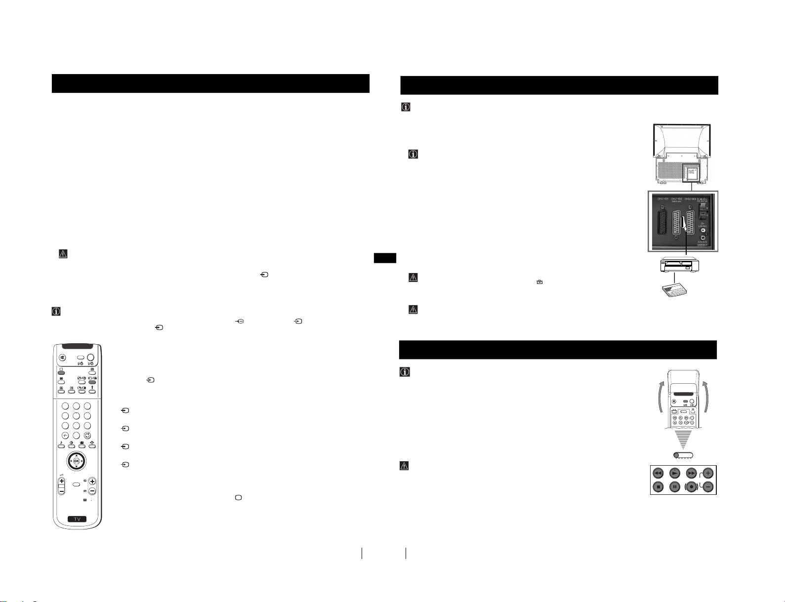
29
GB
Additional Information when connecting equipment
Connecting a VCR
We recommend you connect your VCR to the B or C socket using a scart lead. If you do not have a scart lead, use the “Manually
Tuning the TV” section of this instruction manual to tune in the channel of the VCR test signal to TV programme number “0”.
Also refer to your VCR instruction manual to get the VCR test signal.
If your video supports Smartlink please refer to the "Smartlink" section of this instruction manual.
Connecting to External Audio Equipment
1 To listen to the audio of the set on the Hi-Fi equipment:
Plug in your Hi-Fi equipment to the E sockets on the rear of the set if you wish to amplify the audio output
from the TV.
The output level from E sockets can be varied by adjusting the volume of the headphones. Refer to the “Adjusting the sound”
section of this instruction manual to adjust the volume of the headphones.
2 To listen to the Dolby Prologic system sound on the set speakers:
Plug in your Dolby Prologic system decoder amplifier to the D socket on the rear of the set if you wish to listen to the audio
output from your equipment on the TV speaker. If you have a Dolby amplifier, connect the centre output from your amplifier
to the D socket to use the set as a centre speaker. Refer to the “Using the Features menu” section of this instruction manual
and set the option “Speaker” to “Centre in”.
Remember that the maximum input level of this input is 30 W. Be careful never to over this limit.
For mono equipment
Connect the phono plug to the L/G/S/I socket on the front of the TV and select the 4 input signal using the instructions on
this page below.
Select and View the Input Signal
In order to get the input signal of a connected equipment onto the TV screen, you need to select the symbol of the
connector to which you have connected the device.
e. g. : Your VCR is connected to the connector with the symbol
Y
1/ 1. Press the button on the remote control
repeatedly until you see the symbol 1 on the screen.
Optional Connections
S
RM
903
PROGR
MENU
1
4
7
2
5
8
0
3
6
9
TV
V
I
D
E
O
Optional Connections
Using Optional Equipment
1
Connect your equipment to the designated socket, as it is indicated on the previous page.
2
Switch on the connected equipment.
3
Press the button repeatedly on your remote control until the correct input symbol
appears on the screen.
Symbol Input signals
11
11
• Audio/video input signal through the Scart connector A or * RGB
through Scart connector A.
22
22
• Audio/Video input signal through the Scart connector B or * S Video
through Scart connector B.
33
33
• Audio/Video input signal through the Scart connector C or * S Video
through Scart connector C.
44
44
• S Video input signal through the 4-pin DIN connector F or * video input
signal through phono jack G and audio input signal through phono jacks H.
* (automatic detection of the signal according to the connected equipment)
4
To return to the normal TV picture, press the button on the remote control.
30
Optional Connections
Optional Connections
Smartlink is a direct link between the set and a VCR.
For Smartlink you need:
• A VCR which supports Smartlink, NextView Link, Easy Link or Megalogic.
Megalogic is a trademark of Grundig Corporation.
EasyLink is a trademark of Philips Corporation.
• A fully-wired 21 pin SCART cable to connect your VCR to the Scart connector :2/q2
(SMARTLINK) on the rear of the set.
The features of Smartlink are:
• Tuning information such as the channel overview are downloaded from the set to the VCR.
• Direct recording: While watching TV you need to press just one button on the VCR to record
this programme.
• Automatically switching on: With the set in standby mode, pressing the “Play z” button on
your VCR automatically switches the TV on.
If you have connected a decoder to a VCR which supports Smartlink feature, select
the menu “Further Programme Preset” in the (Manual Set Up) menu and select
DECODER AV2 to each coded channel. For more details, please refer to the section
"Using the Further Programme Preset function" of this instruction manual.
For more information on Smartlink, please refer to the Instruction Manual of your
VCR.
Smartlink
VCR
Decoder
Using the buttons underneath the cover of the remote control you can
control other Sony equipment.
1
Open the cover of the Remote Control.
2
Set the selector VTR 1234 DVD according to the equipment you want to control:
VTR 1 Beta VCR
VTR 2 8 mm VCR
VTR 3 VHS VCR
VTR 4 Digital Video (DCR-VX 1000/9000 E, VHR-1000)
DVD Digital Video Disk
3
Use the buttons underneath the cover on the remote control to operate the equipment.
• If your equipment has a COMMAND MODE selector, set this
selector to the same position as the VTR 1234 DVD selector on this set Remote Control.
• If the equipment does not have a certain function, the corresponding
button on the remote control will not work.
Remote Control of other Sony Equipment
VIDEO TV
VTR 1 2 3 4 DVD
CH
CH
VTR 1 2 3 4 DVD
Rear
– 19 –
Page 20
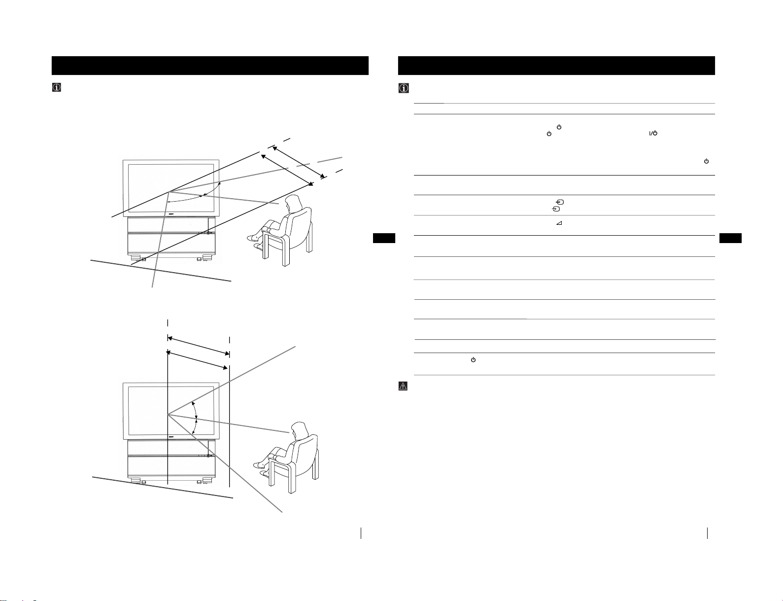
31
GB
Additional Information
Additional Information
For the best picture quality, try to position the set so that you can view the screen from within the areas shown below.
Optimum Viewing Area
Horizontal viewing area
(Optimum viewing position)
Vertical viewing area
(Optimum viewing position)
KP-44PS2: º
KP-51PS2: 60º
KP-44PS2: m
m
inim
um
distance
KP-51PS2: 1.9 m
m
inim
um
distance
KP-44PS2: m
m
inim
um
distance
KP-51PS2: 1.9 m
m
inim
um
distance
KP-44PS2: º
KP-51PS2: 60º
KP-44PS2: º
KP-51PS2: 20º
KP-44PS2: º
KP-51PS2: 20º
KP-44PS2: º
KP-51PS2: 20º
33
GB
Problem
No picture (screen is dark), no sound.
Poor or no picture (screen is dark),
but good sound.
Poor picture quality when watching a
RGB video source.
Good picture, no sound
No colour on colour programmes
Distorted picture when changing
programmes or selecting teletext
Wrong characters appear when viewing
teletext.
Striped picture
Noisy picture when viewing TV channel
Remote control does not function
The standby indicator on the set
flashes.
Additional Information
Additional Information
Here are some simple solutions to the problems which may affect the picture and sound.
Troubleshooting
Solution
• Plug the set in.
• Press the
button on the front of the set.
• If the indicator is on in red colour, press TV button on the remote
control.
• Check the aerial connection.
• Check that the selected video source is on.
• Turn the set off for 3 or 4 seconds and then turn it on again using the
button on the front of the set.
• Using the MENU system, select the Picture Adjustment menu. Adjust the
brightness, contrast and colour balance levels.
• Press the button repeatedly on the remote control until the RGB
symbol 1 is displayed on the screen.
• Press the +/- button on the remote control.
• Check that "Main" speaker is selected in the "Features" menu.
• Using the MENU system, select the Picture Adjustment menu. Adjust the
colour balance.
• Turn off any equipment connected to the Scart connectors on the rear of
the set.
• Using the menu system, enter to the “Language/Country menu and select
the country in which you operate the TV set.
• Adjust the RF Atenuator (ATT). For details, please refer to the section
"Using the Further Programme Preset function".
• Adjust Fine Tuning (AFT) to obtain better picture reception. For details,
please refer to the section "Using the Further Programme Preset function"
• Replace the batteries.
• Contact your nearest Sony service centre.
• If you continue to have these problems, have your TV serviced by qualified personnel.
• NEVER open the casing yourself.
– 20 –
Page 21
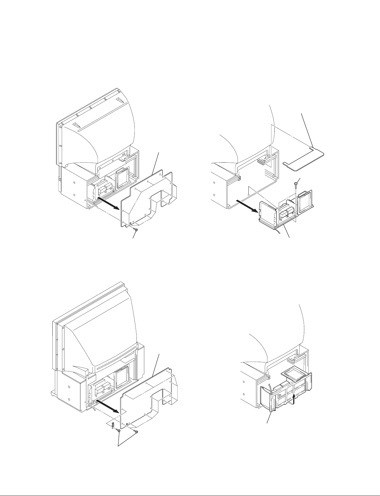
SECTION 3
DISASSEMBLY
KP-44PS2/44PS2U/51PS2
RM-903
3-1. REAR BOARD REMOVAL
• KP-44
3-2. MAIN BRACKET BLOCK
REMOVAL
• KP-44/51
1 Shield board
2 Rear board
2 Two screws
(Hexagon head)
• KP-51
1 Thirteen screws
(Hexagon head)
2 Rear board
3 Main bracket block
3-3. SERVICE POSITION
• KP-44/51
1
1 Thirteen screws
(Hexagon head)
Main bracket block
– 21 –
Page 22
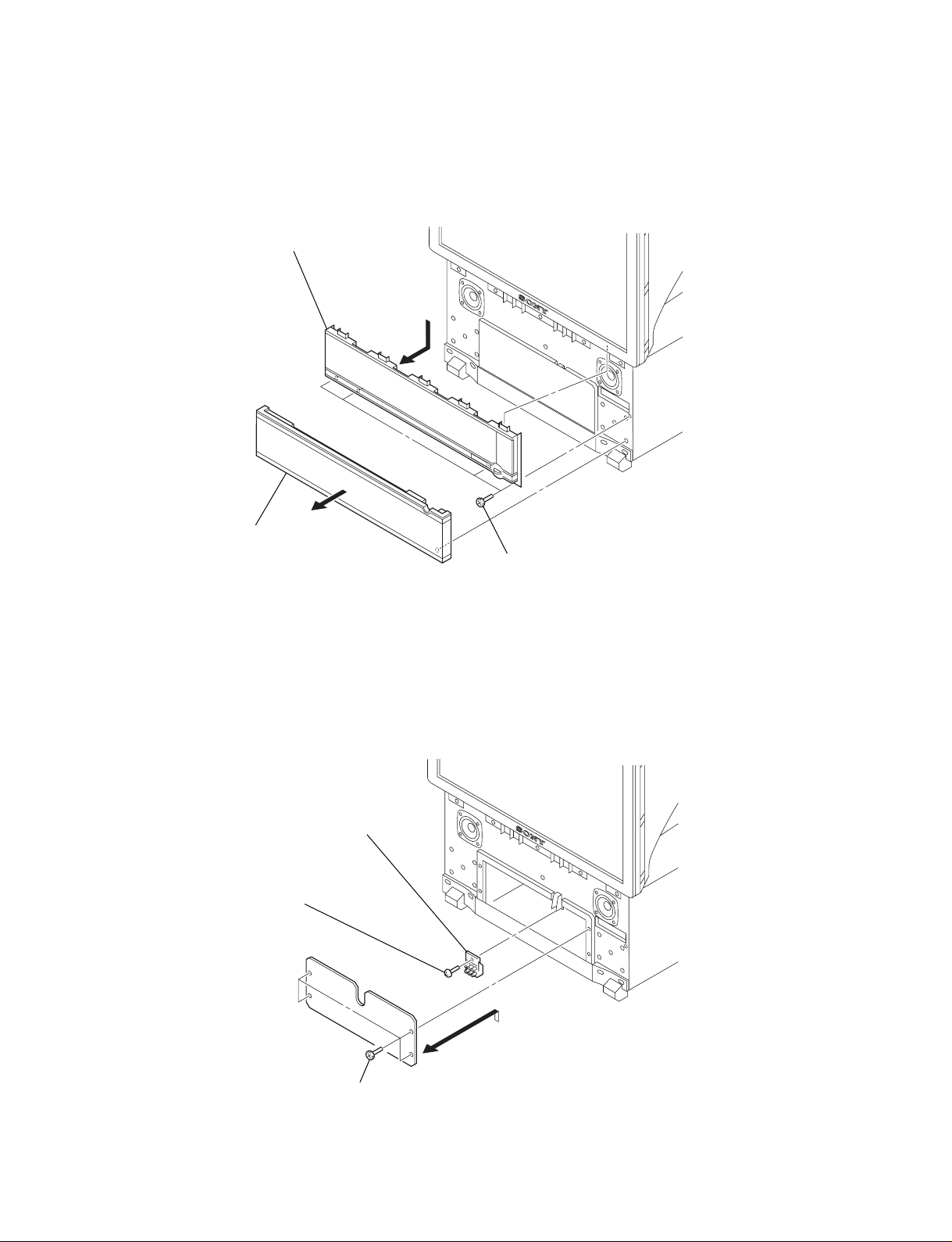
KP-44PS2/44PS2U/51PS2
RM-903
3-4. CONTROL PANEL BLOCK REMOVAL
• KP-44/51
3 Control panel block
1 Front cover
block assembly
2 Four screws
(Hexagon head)
3-5. RESISTOR ASSEMBLY (FOCUS PACK) REMOVAL
• KP-44/51
3 Resistor assembly
(Focus pack)
2 Screw
(+BVTP 4 x 16)
1 Four screws
(Hexagon head): (KP-44)/
Two screws
(Hexagon head): (KP-51)
– 22 –
Page 23
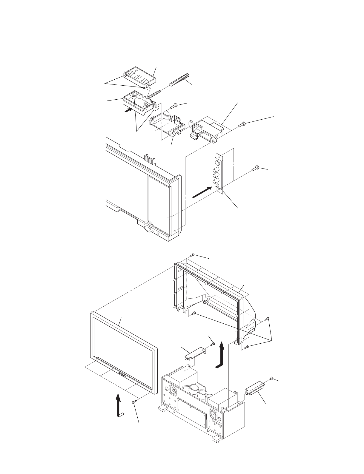
3-6. HB, HA AND CONTROL PANEL BLOCK REMOVAL
!= Control panel block
• KP-44/51
KP-44PS2/44PS2U/51PS2
RM-903
!- Two claws
9 Tray
7
8 Two claws
3-7. BEZNET BLOCK REMOVAL
• KP-44/51
6 Tray bracket
0 Spring (T)
5 Two screws
(+BVTP 4 x 16)
6 Eleven screws
4 HA board
3 Two screw
(+BVTP 4 x 16)
1 Two screw
(+BVTP 3 x 12)
2 HB board
(+BVTP 4 x 16)
9 Beznet block
8 Four screws
(Hexagon head)
3 Screw
(Hexagon head)
(KP-51)
4 Cabinet cover (L)
(KP-51)
7 Mirror cover block
5 Four screws
(Hexagon head)
1 Screw
(Hexagon head)
(KP-51)
2 Cabinet cover (R)
(KP-51)
– 23 –
Page 24
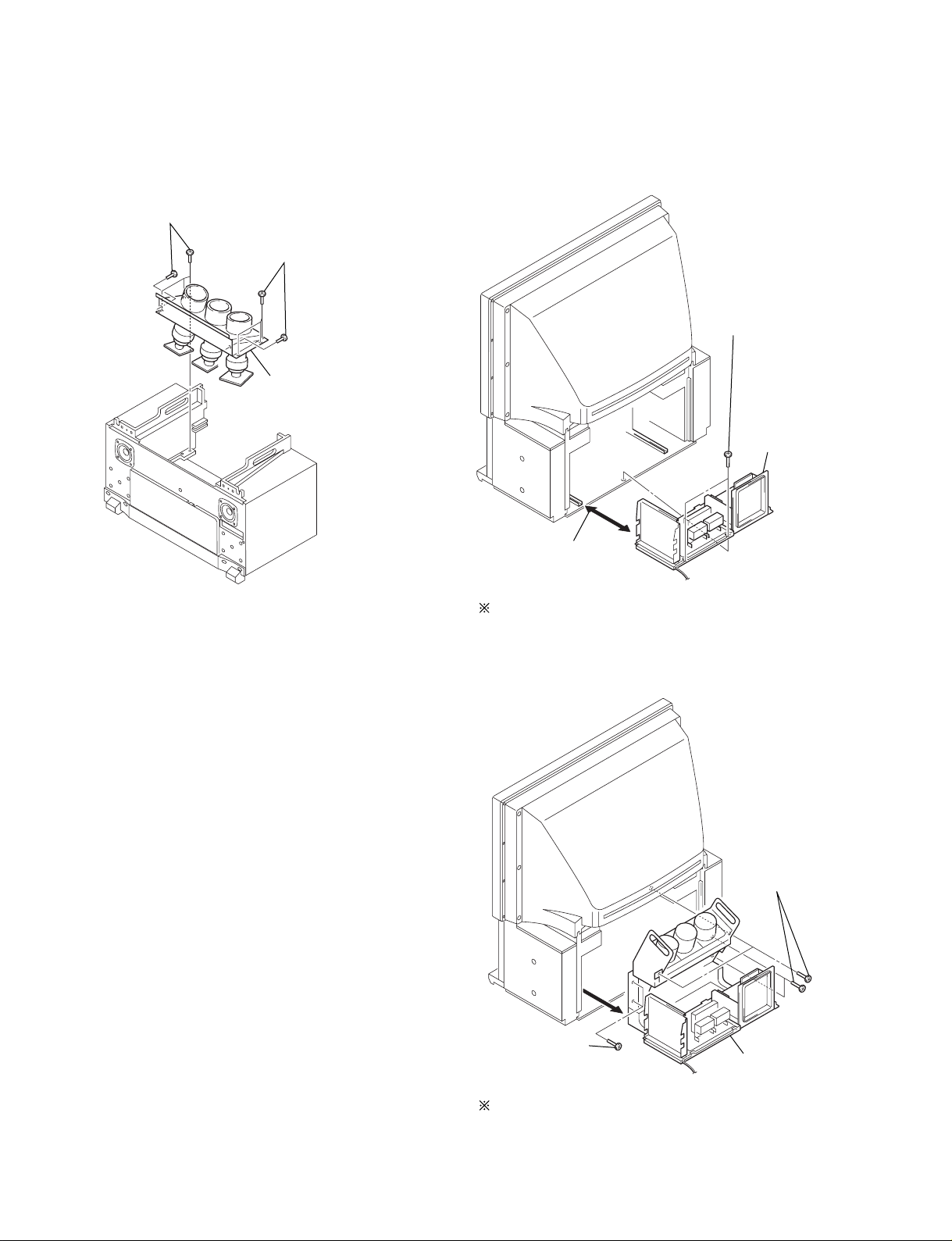
KP-44PS2/44PS2U/51PS2
RM-903
3-8. CHASSIS BLOCK REMOVAL
(1) PICTURE TUBE BLOCK REMOVAL
• KP-44
1 Four screws
(Hexagon head 4 x 20)
1 Four screws
(Hexagon head 4 x 20)
(2) MAIN BRACKET REMOVAL
• KP-51
1 Two screws
(Hexagon head)
2 Picture tube block
2 Pull the main
bracket, and
remove each
connectors
on main bracket.
3 Set the
main bracket.
Pay particular attention to the wires of each Printed circuit
boards when puling out the main bracket.
(3) CHASSIS BLOCK REMOVAL
• KP-51
– 24 –
1 Four screws
(Hexagon head)
1 Two screws
(Hexagon head)
2 Pull out the
chassis block
Pull out the chassis block by gripping the handles as shown in
the diagram.
At this time, pay particular attention to the components
removed in (2).
Page 25
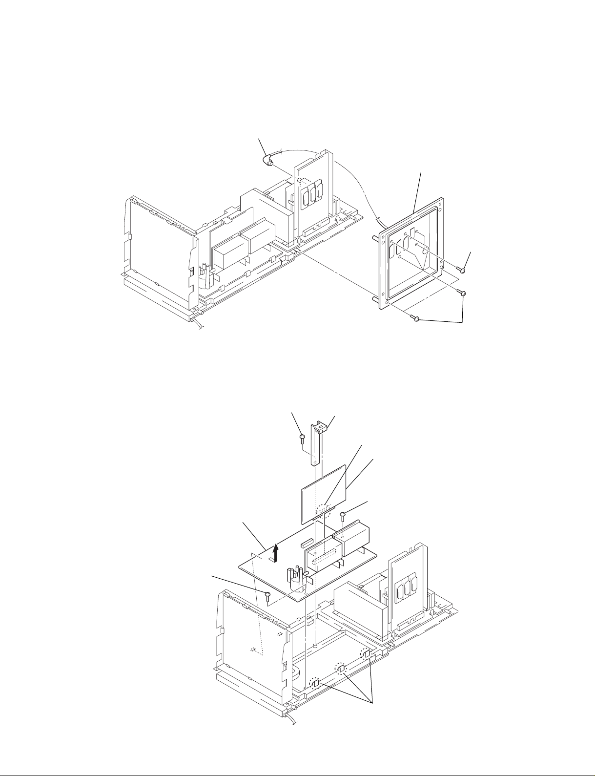
3-9. TERMINAL BOARD REMOVAL
1 RF cable
KP-44PS2/44PS2U/51PS2
RM-903
4 Terminal board
3 Two screws
(+BVTP 3 x 12)
3-10. AP AND D BOARDS REMOVAL
1 Screw
(+BVTP 3 x 12)
7 D board
5 Screw
(+BVTP 3 x 12)
2 Five screws
(+BVTP 4 x 16)
2 Printed circuit
board support
3 Claw
4 AP board
5 Screw
(+BVTP 3 x 12)
– 25 –
6 Three claws
Page 26
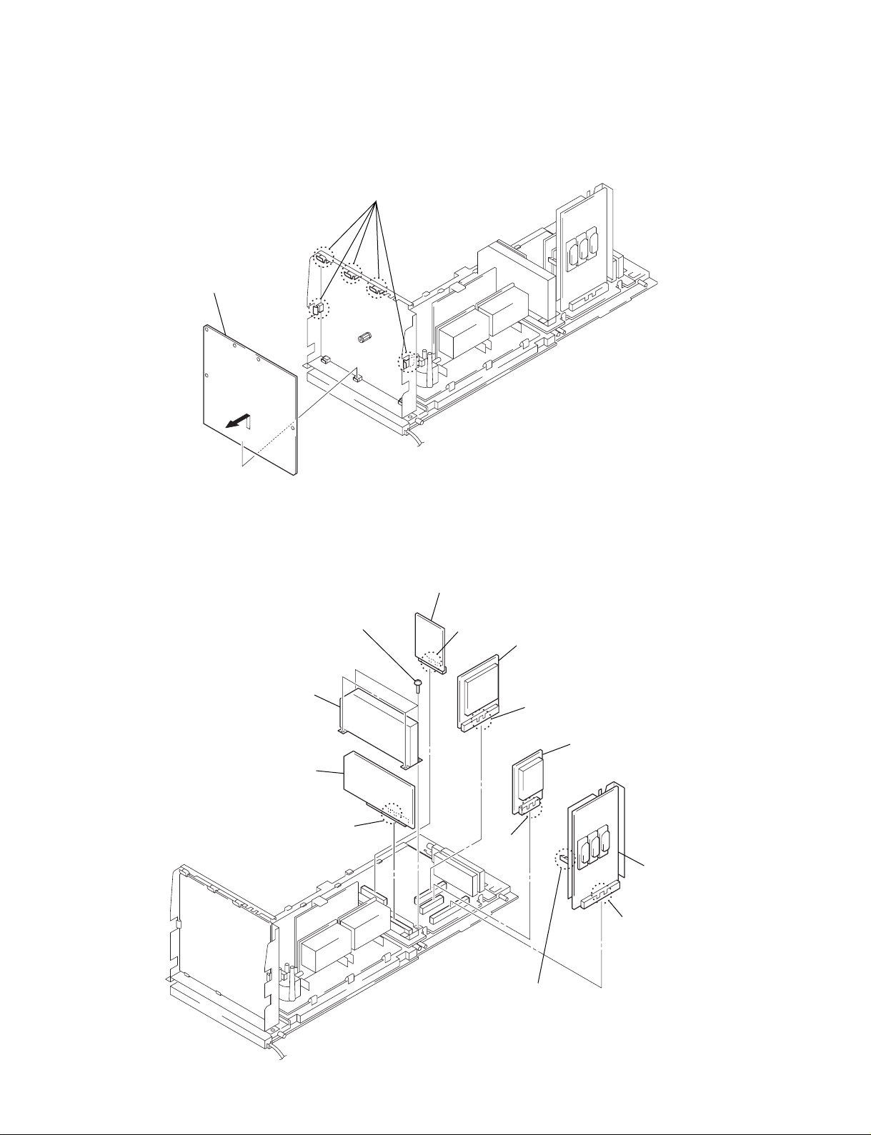
KP-44PS2/44PS2U/51PS2
RM-903
3-11. G BOARD REMOVAL
2 G board
1 Five claws
3-12. J, B3, E, M AND S BOARDS REMOVAL
4 Four screws
(+BVTP 3 x 8)
5 Shield case
7 B3 board
6 Claw
9 E board
8 Claw
!- M board
0 Claw
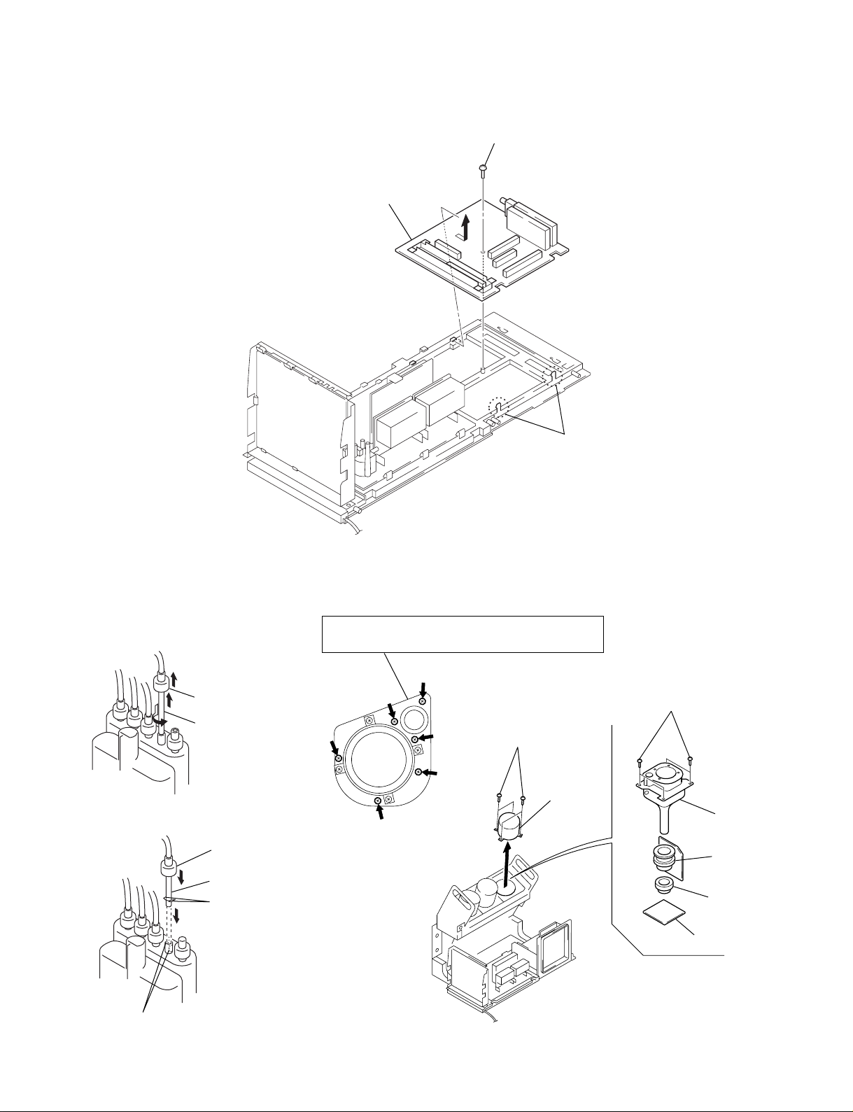
KP-44PS2/44PS2U/51PS2
RM-903
3-13. A BOARD REMOVAL
1 Screw
(+BVTP 3 x 12)
3 A board
2 Two claws
3-14. HIGH-VOLTAGE
CABLE REMOVAL
AND INSTALLATION
(1) Removal
1 Rubber cap
2 HV cable
turn 90°
(2) Installation
2 Rubber cap
1 HV cable
Hook
3-15. PICTURE TUBE REMOVAL
Removing the arrow-marked screw is strictly inhibited.
If removed, it may cause liquid spill
6 Four screws
(+BVTP 4 x 16)
1 Four screws
(+BVTP 4 x 16)
2 Lens
7 Picture
tube
5 Deflection
yoke
4 Neck
assembly
3 CR board
Gutter
– 27 –
Page 28
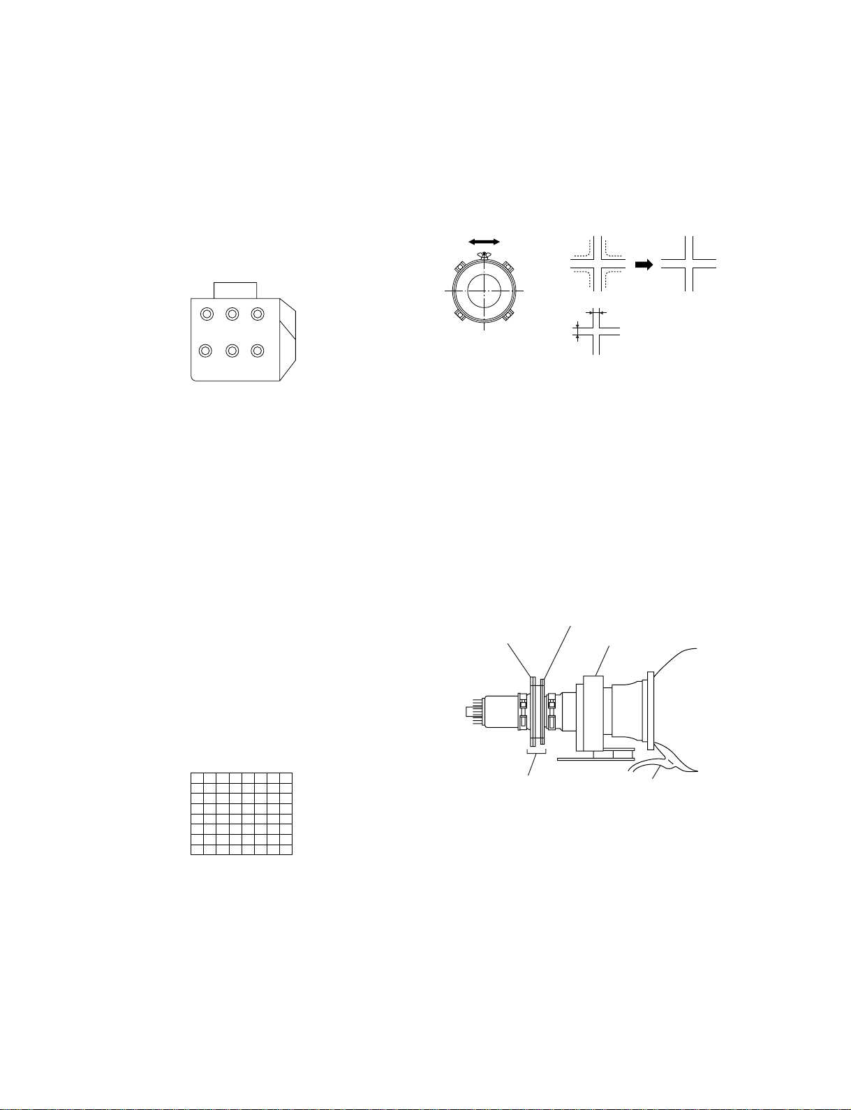
KP-44PS2/44PS2U/51PS2
RM-903
SECTION 4
SET-UP ADJUSTMENTS
4-1. SCREEN VOLTAGE ADJUSTMENT
(ROUGH ALIGNMENT)
1. Receive the Monoscope signal.
2. Set 50% BRIGHTNESS and minimum PICTURE.
3. Turn the red VR on the focus pack all the way to the left and
then gradually turn it to the right until the point where you
can see the retrace line.
4. Next gradually turn it to the left to the position where the
retrace line disappears.
RG
RG
B
SCREEN
B
FOCUS
Focus Pack
Fig. 4-1
4-2. SCREEN (G2) ADJUSTMENT
1. Turn on the power of the set.
2. Select VIDEO1 mode without signals.
3. Supply DC 175 ±0.5 V from external power supply to
TP7103 (KR), TP7203 (KG) or TP7303 (KB) of CR board,
CG board and CB board.
3. Adjust red, green and blue screen voltage to until retrace
line disappears with screen VR on the focus pack.
5. Rotate the green lens and align to obtain the best lens focus
at the center area.
6. Rotate the green focus VR on the focus pack and align to
obtain the best electrical focus in the top right corner.
7. Perform the same alignment for red and blue lenses and electric focus.
8. Fix lens screw.
A
Minimize both A and B.
Lens
Fig. 4-3
B
Fig. 4-4
4-4. DEFLECTION YOKE TILT ADJUSTMENT
1. Receive the Monoscope signal.
2. Place the caps on the red and blue lens so that only the green
color.
3. Loosen the deflection yoke setscrew and align the tilt of the
Deflection yoke so that the bars at the center of the
monoscope pattern are horizontal.
4. After aligning the deflection yoke, fasten it securely to the
funnel-shaped portion (neck) of the CRT.
5. The tilt of the deflection yoke for red and blue is aligned the
same as was done for green.
4-3. FOCUS ROUGH ADJUSTMENT
1. Loose the lens screw.
2. Enter the TT mode. (Refer to SECTION 6.)
3. Place the caps on the red and blue lens so that only the green
color is shown.
4. Press “MENU” twice on the commander and select “Device
Register Setting” b “Projector Engine”, press “6” three
times on the Commander to display the test signal (crosshatch) on the screen.
Test signal
Fig. 4-2
4-pole magnet
2-pole magnet
Neck Assy
Make sure deflection yoke is
touching CRT closely.
Fig. 4-5
Deflection yoke
Anode cap
– 28 –
Page 29
KP-44PS2/44PS2U/51PS2
RM-903
4-5. 2-POLE MAGNET ADJUSTMENT
1. Receive the Dot signal.
2. Place the caps on the red and blue lens so that only the green
color is shown.
3. Turn the green focus VR on the focus pack to the right and
set to over focus to enlarge the spot.
4. Now align the 2-Pole Magnet so that the enlarged spot is in
the center of the just focus spot.
(center of the dot doesn't move)
5. Align the green focus VR and set for just (precise) focus.
6. Perform the same alignment for red and blue.
Use the center dot
Fig. 4-6
4-6. 4-POLE MAGNET ADJUSTMENT
1. Receive the Dot signal.
2. Place the caps on the red and blue lens so that only the green
color is shown.
3. Turn the green focus VR on the focus pack to the left and set
to under focus to enlarge the spot.
4. Now align the 4-Pole Magnet so that the enlarged spot becomes a perfect circle.
5. Perform the same alignment for red and blue.
4-7. GREEN, RED AND BLUE FOCUS
ADJUSTMENT
4-7-1. Green, Red and Blue Lens Focus Adjustment
1. Receive the Monoscope signal.
2. Place the caps on the red and blue lens so that only the green
color is shown.
3. Rotate the green lens and adjust to obtain the best lens focus
at the center area.
4. Fix lens screw.
5. Repeat above process for red and blue.
4-7-2. Green, Red and Blue Electrical Focus
Adjustment
1. Receive the Monoscope signal.
2. Place the caps on the red and blue lens so that only the green
color is shown.
3. Rotate the green focus VR on the focus pack and adjust to
obtain the best electrical focus at the center area.
4. Repeat above process for red and blue.
Use the center dot
Fig. 4-7
OKNG NG
Adjust Point
Fig. 4-8
– 29 –
Page 30
KP-44PS2/44PS2U/51PS2
RM-903
SECTION 5
SAFETY RELATED ADJUSTMENT
When replacing the following components marked with ] on
the schematic diagram, always check hold-down voltage and
if necessary re-adjust.
Part Replaced ([)
R9901
Part Replaced (])
D Board C5123, C5127, C5130, C5143, D5115,
D5204, Q5104, R5136, R5138, R5140,
R9901, T5102, T5104, T5103 (FBT)
5-1. HV HOLD-DOWN ADJUSTMENT
1. Connect HV static voltmeter to HV Block.
2. Mount a resistor (R9901 : 43 k , 1/4 W, METAL
FILM) at CN5003.
3. Remove CN5002 and connect External Power Supply to
CN5002 1 pin (+135 V) and 2 pin (GND).
4. Turn on the set.
Power
Supply
+
–
Fig. 5-1
Remove the cap off
from the unused
terminal and connect a
HV static voltmeter
there.
1
CN5002
2
D BOARD
CN5002
– CONDUCTOR SIDE –
CN5003
Fig. 5-3
CN5003
R9901
Fig. 5-4
5. Receive the Dot signal and set PICTURE/BRIGHTNESS
to minimum.
6. Slowly up the supply voltage from 0 V to 135 V until
hold-down circuit works (picture disappear).
7. Read the HV static voltmeter of peak HV voltage.
Spec : 33.7 ~ 35.3 kV
8. If Hold-down voltage is less than 33.7 kV then replace
R9901 of 43 k with that of 39 k , and check if the
voltage is within the spec.
9. If hold-down voltage is over than 35.3 kV then replace
R9901 of 43 k with that of 47 k , and check if the voltage is within the spec.
Fig. 5-2
– 30 –
Page 31

SECTION 6
Enter the
“TT MODE”
5
(DIGIT 5) (VOLUME +) (TV MODE)ON SCREEN
DISPLAY
(
)
ELECTRICAL ADJUSTMENTS
KP-44PS2/44PS2U/51PS2
RM-903
6-1. ADJUSTMENTS WITH COMMANDER
Service adjustment to this model can performed with the supplied remote commander RM-903.
MUTE
TV MODE
JOYSTICK
VOLUME +
MENU
1
4
7
2
5
8
0
OK
MENU
SONY
TV
VIDE O TV
3
6
9
PROGR
RM
903
RM-903
6-1-1. How to Select Each Mode
The adjustment requires the following modes:
TV STANDBY
ON SCREEN
DISPLAY
SCREEN
FORMAT
Wide
Zoom
14 : 9
4 : 3
Smart
3. Selection of Screen Format
1) Press “ (BLUE)” button on the commander.
2) Press v or V key on the joystick to select “Wide”, “Zoom”,
“14 : 9”, “4 : 3” or “Smart”, and press “ (OK)” button. At
this time, normal screen comes back. (In the TT mode, the
menu is switched to the Service menu.)
6-1-2.How to Enter TT Mode
1. Turn on the main power switch to place this set in standby
mode. (LED will light in red.)
2. Press the buttons on commander as follows, and the TT
mode will be selected.
“TT - -” will appear in the top right corner of the screen.
Other status information will also be displayed.
3. If “ (TV MODE)” button or “- ” + “- ” button is
pressed, the set exits from the TT mode and returns to normal TV mode.
6-1-3.How to Enter Service Menu
1. Enter the TT mode.
2. Press “MENU” button on the commander once, and normal
menu screen will appear, or press it once more, and the following service menu screen will appear.
Service AE5(A)
Wide Zoom 14 : 9 4 : 3 Smart
DRC 100 (PAL) aaa× a
DRC 50 (PAL) aaa× a
DRC 100 (NTSC) aaa× a
DRC 50 (NTSC) aaa× a
1. Selection of Mode Between PAL and NTSC
PAL mode : Enter PAL signal.
NTSC mode: Enter NTSC signal. (VIDEO input only)
2. Selection of Digital Mode
1) Press “MENU” button on the commander, and the menu
screen will appear.
2) Press B key on the joystick to enter the “Picture Adjustment” menu.
3) Press v or V key on the joystick to select “Digital Mode”,
and press B key.
4) Press v or V key on the joystick to select“Normal”,
“DRC50” or “DRC100”, and press “
5) Press “MENU” button to return to normal screen.
(In the TT mode, the menu is switched to the Service menu)
(OK)”.
Initialising
Reset Devices
Monitoring
Device Register Setting
Special Adjustment
Select : v V Next menu : B
3. Following the screen, press v or V key on the joystick to
select the desired item, and press B key to enter the selected
item.
4. Press v or V key on the joystick to change data of each item,
and press “
(OK)” button to write changed data.
(Except Projector Engine mode)
5. To return from each item, press b key on the joystick. Or, to
return to the TT mode, press the “MENU” button.
(Except Projector Engine mode)
– 31 –
Page 32

KP-44PS2/44PS2U/51PS2
RM-903
6-1-4. Screen Display for Service Menu
If each item of service menu is selected, the following screen is
displayed.
• Initialising
Initialising
Model Setting
Destination Setting
Basic Setting
Feature Setting
Select : v V Next menu : B
• Initialising b Model Setting
Model Setting
1 KV-29FX60
2 KV-29FC60
3 KV-29FS60
4 KV-28FX60
5 KV-32FX60
6 KV-32FS60
7 KV-28FC60
8 KV-32FC60
9 KV-28FC60Z
10 KV-32FC60Z
11 KV-28FS70
12 KV-32FS70
13 KV-36FS70
14 KP-48PS1
15 KP-53PS1
16 KP-61PS1
17 KP-44PS2
18 KP-51PS2
19 KF-50SX100
Select : v V Last menu : b Set Model : B
• Initialising b Basic Setting
Basic Setting
No Descr. Min Max Data
1 Sys. B/G OFF ON ON
2 Sys. D/K OFF ON ON
3 Sys. L OFF ON ON
4 Sys. I (UK) OFF ON ON
5 Sys. I (IRL) OFF ON ON
6 TXT Nat. Option 1 4 3
7 Simple PAT OFF ON OFF
8 16 : 9 CRT OFF ON ON
9 Sub-Woofer OFF ON OFF
10 Auto Stand-By OFF ON ON
11 Comb-Filter OFF ON ON
12 Auto YC det OFF ON ON
13 Auto Comb det OFF ON ON
14 AV2 Available OFF ON ON
15 AV3 Available OFF ON ON
16 AV4 Available OFF ON ON
17 AV3 Front & Rear OFF ON OFF
18 SECAM Tape OFF ON ON
19 AV1 Sound Mute OFF ON OFF
Select : v V Last menu : b Enter Item : B
• Initialising b Feature Setting
Feature Setting
No Descr. Min Max Data
1 PAP OFF ON ON
2 PAT OFF ON ON
3 INDEX OFF ON ON
4 EPG OFF ON ON
5 Full EPG OFF ON ON
6 PictBoostBypass OFF ON OFF
Select : v V Last menu : b Enter Item : B
• Initialising b Destination Setting
Destination Setting
Multi
A
B
D
E
K
R
U
Select : v V Last menu : b Set Dest. : B
• Reset Devices
Reset Devices
Backend
Deflection
Ext. Deflection
Dynamic Convergence
Colour Decoder 1
Colour Decoder 2
Audio/Video Switch
MID-X
External PLL MID-X
Panorama Chip
Autowide
Sound
Picture Booster
Select : v V Last menu : b Reset Dev. : B
– 32 –
Page 33

KP-44PS2/44PS2U/51PS2
RM-903
• Monitoring
Monitoring
Device Status Monitor
Error Monitor
Production Monitor
NVM Monitor
Format Monitor
CNI Monitor
Select : v V Next menu : B
• Device Register Setting
Device Register Setting
Backend
Deflection
Ext. Deflection
Dynamic Convergence
Colour Decoder 1
Colour Decoder 2
Audio/Video Switch
MID-X
External PLL MID-X
Panorama Chip
Autowide
Sound
Projector Engine
Picture Booster
Select : v V Next menu : B
• Device Register Setting b Backend
Backend
No Descr. Def. Min Max Data
1 D-Col OFF OFF ON OFF
2 Contrast 44 0 63 31
3 Limit-Lvl 3 0 3 3
4 Hue 32 0 63 32
5 Colour 31 0 63 26
6 CTI-Level 2 0 3 2
7 Brightness 31 0 63 31
8 Gamma 3 0 3 3
9 Sharpness 31 0 63 16
10 R-Drive 31 0 63 27
11 G-Drive 31 0 63 31
12 B-Drive 31 0 63 25
13 Sub Bright 31 0 63 31
14 VM-Level 2 0 3 2
15 R-Cutoff 31 0 63 31
16 Pre/Over 2 0 3 2
17 G-Cutoff 31 0 63 31
18 DPIC-Level 1 0 3 1
19 B-Cutoff 31 0 63 31
20 DC-Tran. 0 0 3 0
21 Sub-Cont. 10 0 15 10
22 LRGB2-Lvl 8 0 15 8
23 P-Abl 15 0 15 15
24 Sharp. F0 ON OFF ON ON
25 CB-Offset1 7 0 15 7
26 CR-Offset1 7 0 15 7
27 CB-Offset2 7 0 15 7
28 CR-Offset2 7 0 15 7
29 Sub Colour 0 –8 8 –1
Select : v V Last menu : b Enter Item : B
– 33 –
Page 34

KP-44PS2/44PS2U/51PS2
RM-903
• Device Register Setting b Deflection
Deflection
No Descr. Def. Min Max Data
1 V-Size 31 0 63 34
2 V-Position 31 0 63 36
3 V-Comp 1 0 3 1
4 V-Linear 7 0 15 7
5 S-Corr 7 0 15 7
6 H-Size 31 0 63 51
7 Ew-Dc OFF OFF ON OFF
8 Pin-Amp 31 0 63 31
9 Up-CPin 31 0 63 31
10 M-Pin 2 0 3 2
11 Lo-CPin 31 0 63 31
12 Trapezium 7 0 15 7
13 H-Position 31 0 63 47
14 AFC-Bow 7 0 15 7
15 AFC-Angle 7 0 15 7
16 Up-Vlin 0 0 15 0
17 Lo-Vlin 0 0 15 0
18 MPIP PAmp –5 –10 10 –5
19 MPIP UCPin 0 –10 10 0
20 MPIP LCPin 0 –10 10 0
21 MPIP Trap 0 –10 10 0
22 EPG PAmp –3 –10 10 –3
23 EPG UCPin 0 –10 10 0
24 EPG LCPin 1 –10 10 1
25 EPG Trap 0 –10 10 0
Select : v V Last menu : b Enter Item : B
• Device Register Setting b Dynamic Convergence
Dynamic Convergence
No Descr. Def. Min Max Data
1 Range 63 0 63 63
2 H stat 33 0 63 33
3 H amp l 37 0 63 37
4 H amp r 36 0 63 36
5 Up Y 31 0 63 31
6 Low Y 33 0 63 33
7 Y up l 30 0 63 30
8 Y up r 30 0 63 30
9 Y low l 31 0 63 31
10 Y low r 30 0 63 30
11 Mbow up l 31 0 63 31
12 Mbow up r 32 0 63 32
13 Mbow low l 32 0 63 32
14 Mbow low r 32 0 63 32
15 V stat 32 0 63 32
16 TCorPCtrl OFF OFF ON OFF
17 TopCorPin 31 0 63 31
18 BCorPCtrl OFF OFF ON OFF
19 BotCorPin 31 0 63 31
Select : v V Last menu : b Enter Item : B
• Device Register Setting b Colour Decoder 1
Colour Decoder 1
• Device Register Setting b EXT. Deflection
EXT. Deflection
No Descr. Def. Min Max Data
1 Linearity 127 0 255 127
2 H Centre 31 0 63 31
3 H Trap 31 0 63 31
4 Rotation 0 0 255 0
5 FocusPhase 127 0 255 127
Select : v V Last menu : b Enter Item : B
No Descr. Def. Min Max Data
1 TINT 31 0 63 31
2 SUB COLOUR 7 0 15 7
3 SUB CONTR 7 0 15 7
4 SHARP GAIN 8 0 15 8
5 Y-OUT LEV. 50 0 63 40
6 C-OUT LEV. 50 0 63 45
7 Y-DL 8 0 10 3
8 Cr OFF. 1 7 0 15 7
9 Cb OFF. 1 7 0 15 7
10 Cr OFF. 2 7 0 15 7
11 Cb OFF. 2 7 0 15 7
12 V CD FREQ 3 0 7 3
13 V CD MODE 1 0 3 1
14 MVM OFF OFF ON OFF
15 S R-Y ADJ 7 0 15 7
16 S B-Y ADJ 2 0 15 5
17 BELL/HPF 2 0 3 2
18 BELL F0 OFF OFF ON OFF
19 S GP 0 0 3 0
Select : v V Last menu : b Enter Item : B
– 34 –
Page 35

KP-44PS2/44PS2U/51PS2
RM-903
• Device Register Setting b Colour Decoder 2
Colour Decoder 2
No Descr. Def. Min Max Data
1 TINT 31 0 63 31
2 SUB COLOUR 7 0 15 7
3 SUB CONTR 7 0 15 7
4 SHARP GAIN 8 0 15 8
5 Y-OUT LEV. 50 0 63 31
6 C-OUT LEV. 50 0 63 45
7 Y-DL 8 0 10 3
8 Cr OFF. 1 7 0 15 7
9 Cb OFF. 1 7 0 15 7
10 Cr OFF. 2 7 0 15 7
11 Cb OFF. 2 7 0 15 7
12 V CD FREQ 3 0 7 3
13 V CD MODE 1 0 3 1
14 MVM OFF OFF ON OFF
15 S R-Y ADJ 7 0 15 7
16 S B-Y ADJ 2 0 15 5
17 BELL/HPF 2 0 3 2
18 BELL F0 OFF OFF ON OFF
19 S GP 0 0 3 0
Select : v V Last menu : b Enter Item : B
• Device Register Setting b MID-X
• Device Register Setting b External PLL MID-X
External PLL MID-X
No Descr. Def. Min Max Data
1 VCO7-0PAL 184 0 255 184
2 VCO7-0NTSC 172 0 255 172
3 VCO11-8 6 0 15 6
4 DIV1, 2, 4, 8 2 0 3 2
5 Fine Delay 0 0 63 0
6 Coar. Delay 0 0 3 0
7 Ch. Pump 0 0 3 0
8 PD Pol. ON OFF ON ON
9 DSync Wdth 3 0 3 3
10 Dsync Del OFF OFF ON OFF
11 Sync Pol ON OFF ON ON
12 DSync Pol ON OFF ON ON
13 Clk En ON OFF ON ON
14 NClk En OFF OFF ON OFF
15 Clk/2 En OFF OFF ON OFF
16 NClk/2 En OFF OFF ON OFF
17 DSync En ON OFF ON ON
18 Unlock En OFF OFF ON OFF
19 VCO Bypass ON OFF ON ON
20 Synth Pwr ON OFF ON ON
21 Rdout Pwr OFF OFF ON OFF
22 DIVOUT En ON OFF ON ON
23 DSync Byp OFF OFF ON OFF
24 DSync Hold OFF OFF ON OFF
Select : v V Last menu : b Enter Item : B
MID-X
No Descr. Def. Min Max Data
1 M H POS 0 –31 31 0
2 S H POS 0 –8 8 0
3 D YS SEL 1 0 3 1
4 D YS DELAY 7 0 7 7
5 D SYNC MOD ON OFF ON ON
6 Text Sharp OFF OFF ON OFF
Select : v V Last menu : b Enter Item : B
• Device Register Setting b Panorama Chip
Panorama Chip
No Descr. Def. Min Max Data
1 ROM speed 25 0 255 25
2 Prog. No. 0 0 11 3
3 HSize Offs 3 0 15 3
4 IMODE 0 0 255 0
5 Disable OFF OFF ON OFF
6 Send AUX OFF OFF ON OFF
7 AUX0 67 0 255 67
8 AUX1 0 0 255 0
9 AUX2 68 0 255 68
10 AUX3 0 0 255 0
11 AUX4 12 0 255 12
12 AUX5 81 0 255 81
13 AUX6 7 0 255 7
14 AUX7 0 0 255 0
15 AUX8 65 0 255 65
16 AUX9 244 0 255 244
17 AUX10 32 0 255 32
18 AUX11 209 0 255 209
19 AUX12 7 0 255 7
20 AUX13 0 0 255 0
Select : v V Last menu : b Enter Item : B
– 35 –
Page 36

KP-44PS2/44PS2U/51PS2
RM-903
• Device Register Setting b Autowide
Autowide
No Descr. Def. Min Max Data
1 Upara ON OFF ON ON
2 Upthin OFF OFF ON OFF
3 Enjtoz OFF OFF ON OFF
4 X149J ON OFF ON ON
5 Syncslc OFF OFF ON OFF
6Tm 1 0 3 1
7 Uprlvl OFF OFF ON OFF
8 Ofslvl OFF OFF ON OFF
9 Alpf 3 0 3 3
10 eddec2 3 0 3 3
11 Lnstblz ON OFF ON ON
12 Lnhys OFF OFF ON OFF
13 Drkpri ON OFF ON ON
Select : v V Last menu : b Enter Item : B
• Device Register Setting b Sound
Sound
No Descr. Def. Min Max Data
1 Carr.-Mute ON OFF ON ON
2 SCART1 Vol 79 0 127 79
3 SCART2 Vol 79 0 127 79
4 SCART-Pr. 27 0 127 27
5 I2S1-Pr. 16 0 127 16
6 I2S2-Pr. 16 0 127 16
7 FM Pr. 27 0 127 27
8 BG Nic. Pr. 53 0 127 53
9 L Nic. Pr. 59 0 127 59
10 DK Nic.Pr. 53 0 127 53
11 I Nic. Pr. 97 0 127 97
12 Irl NicPr. 97 0 127 97
13 SubW. Vol. 0 –127 0 0
14 Bass Offs 0 –3 3 0
15 TrebleOffs 2 –3 3 2
16 Loudn. Offs 0 0 9 0
17 HP-VolOffs –2 –5 5 –2
18 M-S Limit 30 –128 127 30
19 M-B Limit –30 –128 127 –30
20 S-M Limit 12 –128 127 12
21 S-B Limit –20 –128 127 –20
22 B-M Limit –12 –128 127 –12
23 B-S Limit 20 –128 127 20
24 Err. Max 40 0 255 40
25 Err. Min 18 0 255 18
26 Vol.Offset –3 –6 0 –3
• Device Register Setting b Picture Booster
Picture Booster
No Descr. Def. Min Max Data
1 DEM OFF OFF ON OFF
Select : v V Last menu : b Enter Item : B
• Special Adjustment
Special Adjustment
No Descr. Min Max Data
1 RGB Level 0 7 0
2 RGB Gain 0 31 6
3 RGB PAT Level 0 7 0
4 RGB PAT Gain 0 31 12
5 Extra FW 0 255 255
6 EPG ChkS Check OFF ON ON
7 Slicer High OFF ON ON
8 FCW Wide OFF ON OFF
9 Mpeg NR OFF ON OFF
10 Notch Filter OFF ON OFF
11 NLD step –7 0 –1
12 PKD step –15 0 –5
13 CRD step 0 15 5
14 SHP step –7 0 –5
15 COL step –7 0 –1
16 NTSC AutoYc AV2 OFF ON ON
17 NTSC AutoYc AV3 OFF ON ON
18 RGB Disable OFF ON OFF
19 Telop C/M OFF ON ON
20 Intern GD OFF ON OFF
21 AV2 YC mix out OFF ON OFF
22 Line 318 TXT OFF ON OFF
Select : v V Last menu : bEnter Item : B
Select : v V Last menu : b Enter Item : B
– 36 –
Page 37

Name/Description
KP-44PS2/44PS2U/51PS2
RM-903
Standard Data
: Fixed data. xxxx : Cannot change.
000000
000000
00
00
59
15151515
35172309
5011001440880
994211652
26
26
00
26
31
239648
20
37
14
01
1056
4095
14
01
1056
4095
14
00
4095
1056
71339346
67
00
00
00
100
1110
67
100
1110
67
100
1110
000000000000000000000000000000
—90
—40
127
000000000000000000000000000000
—90
—40
127
00
00
00
00
—90
00
—40
127
00
000000
00
00
00
00
00
00
00
00
00
159
1253
00
00
00
00
00
00
00
00
00
159
1253
00
00
00
00
00
00
00
00
00
00
000000
00
159
1253
00
000000
26
DRC 100 (PAL) DRC 50 (PAL) DRC100 (NTSC) DRC 50 (NTSC)
Wide Zoom 14 : 9 Smart Wide Zoom 14 : 9 Smart Wide Zoom 14 : 9 Smart Wide Zoom 14 : 9 Smart
00, 01
00, 01
00, 01
00 ~ 15
01 ~ 255
Data Range
Item
00 FDIS Switch of display for fine adjustment data
6-1-5. Service List (Projector Engine)
No. Name
01 ~ 255
01 COPY Service copy adjustment
02 ALCP Service all copy adjustment
03 OSDH OSD horizontal position of PJED service menu
04 OSDV 32 75 24 62 OSD vertical position of PJED service menu
05 FVSL 00 14 00 14 00 14 00 14 Start position of fine adjustment
40
00
1056
00 ~ 255
00 ~ 255
00 ~ 255
00 ~ 255
00 ~ 4095
00 ~ 4095
06 FVSP 05 17 15 39 05 16 14 29 Start line of fine adjustment
07 V1DL 01 77 01 148 01 52 01 135 Value of V1 delay
08 V1CU 750 985 375 491 897 1183 449 592 Value of V1 count up
09 V1OH 30 03 Value of V1 offset higher data
10 V1OL Value of V1 offset lower data
11 OEVP Odd/Even select position
14
00
67
100
1110
4095
00 ~ 31
00 ~ 31
00 ~ 4095
12 COHP Horizontal phase for rough adjustment
13 34CS Start center clamp position of H3 and H4 pulse
00 ~ 255
00 ~ 4095
00 ~ 4095
00 ~ 4095
14 34CW Width center clamp position of H3 and H4 pulse
15 FIHP Horizontal phase for fine adjustment
16 TPHP Horizontal phase for test pattern
17 TPVP 26 58 53 117 20 49 47 103 Vertical phase for test pattern
18 DFHP Horizontal phase for dynamic focus
000000000000000000000000000000
—90
—40
127
—128 ~ 127
19 DFHG Value of horizontal parabola wave for dynamic focus
00 ~ 4095
—128 ~ 127
—128 ~ 127
—128 ~ 127
—128 ~ 127
20 DFVG Value of vertical parabola wave for dynamic focus
21 DFDC Value of center for dynamic focus
22 DFV1 Value of V1 saw wave for dynamic focus
23 SDHP Compensation of horizontal phase for shading
24 SDH1 Value of horizontal saw wave for dynamic focus
– 37 –
00 ~ 31
00 ~ 31
00 ~ 31
00 ~ 31
00 ~ 31
00 ~ 31
00 ~ 31
00 ~ 31
00 ~ 31
00 ~ 31
25 RVCS Start position of RED vertical clamp
26 RVCW Width of RED vertical clamp
27 GVCS Start position of GREEN vertical clamp
28 GVCW Width of GREEN vertical clamp
29 BVCS Start position of BLUE vertical clamp
30 BVCW Width of BLUE vertical clamp
31 RHCS Start position of RED horizontal clamp
32 RHCW Width of RED horizontal clamp
33 GHCS Start position of GREEN horizontal clamp
34 GHCW Width of GREEN horizontal clamp
00
00
00
00
00
00
159
1253
00 ~ 31
00 ~ 31
00 ~ 2047
00 ~ 2047
00 ~ 2047
00 ~ 2047
00 ~ 4095
00 ~ 4095
00 ~ 4095
—128 ~ 127
—128 ~ 127
—128 ~ 127
35 BHCS Start position of BLUE horizontal clamp
36 BHCW Width of BLUE horizontal clamp
37 BDVU 23 18 27 21 23 18 27 21 23 18 27 21 23 18 27 21 Vertical position for border line 1
38 BDVL 905 686 1061 811 905 686 1061 811 905 686 1061 811 905 686 1061 811 Vertical position for border line 2
39 BDHL Horizontal position for border line 1
40 BDHR Horizontal position for border line 2
41 HBLD Horizontal phase for output of H.Blank out
42 HBLW Width for output of H.Blank out
43 PWM2 PWM2 output width setting of Regi. IC
44 COGV GREEN vertical center offset data for Auto Regi.
45 CORV RED vertical center offset data for Auto Regi.
46 COBV BLUE vertical center offset data for Auto Regi.
00
00
00
—128 ~ 127
—128 ~ 127
—128 ~ 127
47 COGH GREEN horizontal center offset data for Auto Regi.
48 CORH RED horizontal center offset data for Auto Regi.
49 COBH BLUE horizontal center offset data for Auto Regi.
Page 38

KP-44PS2/44PS2U/51PS2
RM-903
Name/Description
00000000000000000000000000
00000000000000000000000000
Standard Data
00000000000000000000000000
120
120
80
45
45
31
00
475
00
47500930
00
29000560
00
930
13500645
13500645
13500640
1170
000000
00
1170
000000
00
1170
00
00
000/000
000/000
000/000
000/000
000/000
000/000
000/–200
000/–200
000/–200
000/000
xxxx/000
000/000
xxxx/000
000/000
xxxx/000
000/250
000/xxxx
000/250
000/xxxx
000/250
000/xxxx
000/000
000/xxxx
000/000
000/xxxx
000/000
000/xxxx
000/000
000/–200
000/000
000/–200
000/000
000/–200
000/000
xxxx/000
000/000
xxxx/000
000/000
xxxx/000
000/250
000/xxxx
000/250
000/xxxx
000/250
000/xxxx
000/000
000/xxxx
000/000
000/xxxx
000/000
000/xxxx
000/000
000/–200
000/000
000/–200
000/000
000/–200
000/000
xxxx/000
000/000
xxxx/000
000/000
xxxx/000
000/250
000/xxxx
000/250
000/xxxx
000/250
000/xxxx
000/xxxx
000/xxxx
000/xxxx
00
000000
00
00000000000000000000000000
DRC 100 (PAL) DRC 50 (PAL) DRC100 (NTSC) DRC 50 (NTSC)
Wide Zoom 14 : 9 Smart Wide Zoom 14 : 9 Smart Wide Zoom 14 : 9 Smart Wide Zoom 14 : 9 Smart
Data Range
–128 ~ 127
–128 ~ 127
–128 ~ 127
–128 ~ 127
–128 ~ 127
Item
50 SOGV GREEN vertical skew offset data for Auto Regi.
51 SORV RED vertical skew offset data for Auto Regi.
52 SOBV BLUE vertical skew offset data for Auto Regi.
53 SOGH GREEN horizontal skew offset data for Auto Regi.
No. Name
54 SORH RED horizontal skew offset data for Auto Regi.
–128 ~ 127
–128 ~ 127
–128 ~ 127
55 SOBH BLUE horizontal skew offset data for Auto Regi.
56 ZOGH GREEN horizontal size offset data for Auto Regi.
57 ZORH RED horizontal size offset data for Auto Regi.
–128 ~ 127
–128 ~ 127
–128 ~ 127
58 ZOBH BLUE horizontal size offset data for Auto Regi.
59 LOGH GREEN horizontal linearity offset data for Auto Regi.
60 LORH RED horizontal linearity offset data for Auto Regi.
80
00 ~ 255
00 ~ 127
–128 ~ 127
61 LOBH BLUE horizontal linearity offset data for Auto Regi.
62 ERR Auto Regi. Error code
63 ADTM A/D data input timing of Auto Regi.
31
00
29000560
00 ~ 2047
00 ~ 2047
00 ~ 2047
64 VUP Auto Regi. Pattern upper vertical position
65 VUPM Auto Regi. Pattern upper middle vertical position
66 VMID Auto Regi. Pattern middle vertical position
13500640
00 ~ 2047
00 ~ 2047
00 ~ 4095
67 VLOM Auto Regi. Pattern lower middle vertical position
68 VLOW Auto Regi. Pattern lower vertical position
69 HLE Auto Regi. Pattern left horizontal position
00
1170
00 ~ 4095
00 ~ 4095
00 ~ 4095
00 ~ 4095
70 HLEM Auto Regi. Pattern left middle horizontal position
71 HMID Auto Regi. Pattern middle horizontal position
72 HRIM Auto Regi. Pattern right middle horizontal position
73 HRIV Auto Regi. Pattern right horizontal position
000000
00, 01
00 ~ 255
00 ~ 255
74 SFTF Switch of shift fast 00 : Normal 01 : Quick
75 ACTL Account time counter lower byte
76 ACTH Account time counter higher byte
– 38 –
00
000/000
000/000
000/000
000/250
xxxx/000
000/–200
00 ~ 03
–512 ~ 511
–512 ~ 511
–512 ~ 511
–512 ~ 511
–512 ~ 511
–512 ~ 511
LIN GREEN Horizontal/Vertical linearity
PIN GREEN Horizontal/Vertical pincushion
KEY GREEN Vertical keystone
SIZE GREEN Horizontal/Vertical size
CENT GREEN Horizontal/Vertical center
SKEW GREEN Horizontal/Vertical skew
77 SLSW Auto Regi. Adjustment item select
GRN
000/000
000/xxxx
000/xxxx
–512 ~ 511
–512 ~ 511
–512 ~ 511
MLIN GREEN Horizontal mid linearity
MSIZ GREEN Horizontal mid size
CENT BLUE Horizontal/Vertical center
000/000
000/000
000/–200
–512 ~ 511
–512 ~ 511
–512 ~ 511
LIN BLUE Horizontal/Vertical linearity
SIZE BLUE Horizontal/Vertical size
SKEW BLUE Horizontal/Vertical skew
000/250
xxxx/000
–512 ~ 511
–512 ~ 511
PIN BLUE Horizontal/Vertical pincushion
KEY BLUE Vertical keystone
BLU
000/000
000/xxxx
000/xxxx
–512 ~ 511
–512 ~ 511
–512 ~ 511
MLIN BLUE Horizontal mid linearity
MSIZ BLUE Horizontal mid size
CENT RED Horizontal/Vertical center
000/000
000/000
000/–200
–512 ~ 511
–512 ~ 511
–512 ~ 511
LIN RED Horizontal/Vertical linearity
SIZE RED Horizontal/Vertical size
SKEW RED Horizontal/Vertical skew
000/250
xxxx/000
–512 ~ 511
–512 ~ 511
PIN RED Horizontal/Vertical pincushion
KEY RED Vertical keystone
RED
000/xxxx
000/xxxx
–512 ~ 511
–512 ~ 511
MLIN RED Horizontal mid linearity
MSIZ RED Horizontal mid size
Page 39

KP-44PS2/44PS2U/51PS2
RM-903
6-2. REGISTRATION ADJUSTMENT
6-2-1.Setup for Adjustment
1. Marking
1) At the 4 insides of the screen, locate the middle. Use a tape
measure to identify the middle.
: middle
2. Data Setting
1) Set DRC100 (PAL-Wide) mode.
2) Enter the Service menu, and select “Device Register Setting” b “Projector Engine”.
3) Press “7” + “-” (READ) buttons on the commander to read
the data from NVM. Then all the default data are restored.
Note : When you replaced printed circuit boards or devices or
CRTs, and when correction is drastically necessary, press
“5” + “-” (PJE INITIAL) buttons to initialize the data
in the Projector Engine mode.
Press “ (MUTE)” + “-” buttons on the commander to
write the data.
5. Adjust “1 V-Size” and “6 H-Size” so that the picture size is
within the specification.
SPEC Overscan Spec. = 7.5%
Input Signal H SIZE V SIZE
PAL SPCB 16.7 ± 0.1 sq. 12.5 ± 0.1 sq.
1 V -Size
6 H-Size
6. Adjust the following items so as to attain the optimum
picture.
4 V -Linear
5 S-Corr
8 Pin Amp
6-2-2. Main Deflection Adjustment
The data values are same in all modes, and therefore the adjustment for the DRC100 (PAL-Wide) mode only is performed here.
1. Place the caps on the red and blue lenses so that only the
green color is displayed.
2. Enter the PAL SPCB signal to set the DRC100 (PAL) mode.
3. Set the screen format to “Wide”.
4. Enter the Service menu, and select “Device Register Setting” b “Deflection”.
5. Adjust “2 V-Position” and “13 H-Position” so that the picture is displayed in the center of screen.
2 V -P osition
13 H-Position
9 Up-CPin
11 Lo-CPin
12 T r apezium
14 AFC-Bow
15 AFC-Angle
– 39 –
Page 40

KP-44PS2/44PS2U/51PS2
RM-903
6-2-3. Operation Method for Projector Engine
Mode
MUTE
Write data to NVM
TV MODE
Copy data to all
mode
Adjustment item
up
Adjustment item
down
Read data from
NVM
JOYSTICK
VOLUME +
MENU
1
4
7
2
5
8
0
OK
MENU
SONY
TV
VIDE O TV
3
6
9
PROGR
RM
903
TV STANDBY
ON SCREEN
DISPLAY
Copy PAL data
to NTSC
Color change
Internal test signal
Initialize data
(Not stored)
Mode select
(Fine or Rough)
SCREEN
FORMAT
Wide
Zoom
14 : 9
4 : 3
Smart
RM-903
1. Functions of Keys on Commander
• 1 : Changes adjustment item. (item No. moves up)
: Marker moves clockwise from center to out-
side. (in fine adjustment mode)
• 4 : Changes adjustment item.
(item No. moves down)
: Marker moves counterclockwise from outside
to center. (in fine adjustment mode)
• v V b B : Changes data value. (up or down)
: Marker moves up, down, or to the left or right.
(in fine adjustment mode)
• 3 : Changes adjustment color.
(except item No. 00~77) GRN c BLU c RED
• 6 : Displays or changes internal test signals.
: crosshatch + external signal c dot + external
signal c crosshatch only c dot only c off
• 9 : Switches adjustment mode.
rough adjustment mode c fine adjustment
mode
•
(OK) : Switches marker moving method.
(in fine adjustment mode)
joystick (v, V, b, B) keys c 1 and 4 buttons
Commander Function
Buttons Mode Description
+ - WRITE Writes data to NVM.
7 + - READ Reads data from NVM.
5 + - PJE Service data initialization. Not stored.
2 + - PJE Copies and writes data of DRC1250
INITIAL
COPY
+ - PJE Copies data of PAL mode to NTSC mode.
WRT5060
(Be sure not to use usually)
(50Hz) mode to all other modes.
2. Operation Method for Rough Adjustment
1) Enter the Service menu, and select “Device Register Setting” b “Projector Engine”.
2) Press “1” or “4” button on the commander to select the
item, and press v, V, b, B key on the joystick to change the
data.
Item No.
PJE 00 00
FDIS |
Adjustment Item
Data
v, B : Data up
V, b : Data down
3) Select “GRN CENT” . When BLU or RED is displayed,
press “3” button on the commander to change the adjustment color in the order of GRN c BLU c RED.
4) In the GRN, BLU, or RED mode, v, V keys on the joystick
can change the data in vertical direction, or b, B keys in
horizontal direction.
Color
GRN 000 000
CENT
Data (H)
Data (V)
b : Data (H) up
B : Data (H) down
Adjustment Item
v : Data (V) up
V : Data (V) down
5) Before returning to the Service menu, press “
(MUTE)”
+“-” buttons on the commander to write the data.
(Omission of this operation causes the set data to be returned
to the data before adjustment)
6) Press “MENU” button on the commander to return to the
Service menu.
– 40 –
Page 41

KP-44PS2/44PS2U/51PS2
RM-903
3. Operation Method for Fine Adjustment
(in GRN, BLU, or RED Mode)
1) Select the Projector Engine mode.
2) Select FDIS so that the data at each position can be displayed
in the fine adjustment mode, and set the data to “01”.
3) Press “9” button on the commander, and the fine adjustment mode will be active where a green marker appears in
the center of screen (in the case of GRN mode).
4) Press “
switched between green (GRN mode) and white alternately.
5) Use “1” or “4” button on the commander, or the joystick
to move the marker to the position to be adjusted, where fine
adjustment can be made.
• When marker color is white.
(in this case, fine adjustment is disabled)
• When marker color is green. (GRN mode)
(OK)” button, and the marker color will be
Operating the joystick can move the marker
up, down, or to the left or right freely.
6-2-4.Projector Engine Adjustment
(Sub Deflection Adjustment)
Adjustment a : Yes – : No
Adjustment Type
Adjustment Item GRN RED BLU
H / V H / V H / V
CENT a / aa / aa / a
SKEW a / aa / aa / a
SIZE a / aa / aa / a
LIN a / aa / aa / a
KEY – / a – / a – / a
PIN a / aa / aa / a
MLIN a / – a / – a / –
MSIZ a / – a / – a / –
<Adjustment for DRC100 (PAL-Wide) Mode>
1. Green Adjustment
1) Place the caps on the red and blue lenses so that only the
green color is displayed.
2) Enter the PAL SPCB signal to set the DRC100 (PAL) mode.
3) Set the screen format to “Wide”.
4) Select the Projector Engine mode.
5) Press “6” button on the commander to display internal test
signal (crosshatch).
6) Select “GRN CENT”, and adjust so that the picture coincide
in the center of screen.
1 : moves the marker clockwise from center to outside.
4 : moves the marker counterclockwise from outside to center.
• Fine adjustment can be made on the basis of marker
position using v, V, b, B keys on the joystick.
Movement when v key
on joystick is pressed.
CROSSHATCH
Movement when B key
on joystick is pressed.
CROSSHATCH
6) Press “9” button on the commander to return to the rough
adjustment mode.
• GRN CENT (horizontally/vertically)
Push the joystick
to B
Push the joystick
to v
Push the joystick
to b
Push the joystick
to V
– 41 –
Page 42

KP-44PS2/44PS2U/51PS2
RM-903
7) Select “GRN SKEW”, and correct the tilt of horizontal lines
and vertical lines.
• GRN SKEW (horizontally/vertically)
Push the joystick
to B
Push the joystick
to v
Push the joystick
to b
Push the joystick
to V
8) Select “GRN SIZE”, and adjust so that each distance from
center to left end and to right end is equal. Adjust so that
each distance from center to top and to bottom is equal.
• GRN SIZE (horizontally/vertically)
Push the joystick
to B
Push the joystick
to b
10) Select “GRN KEY”, and adjust so that upper and lower hori-
zontal lines on the screen become parallel.
• GRN KEY (vertically)
Push the joystick
to v
Push the joystick
to V
11) Select “GRN PIN”, and adjust so that right and left vertical
lines on the screen become straight. Adjust so that upper and
lower horizontal lines on the screen become straight.
• GRN PIN (horizontally/vertically)
Push the joystick
to B
Push the joystick
to b
Push the joystick
to v
Push the joystick
to V
9) Select “GRN LIN”, and adjust so that each space at the right
end and at the left end of screen is equal. Adjust so that each
space at the top and at the bottom of screen is equal.
• GRN LIN (horizontally/vertically)
Push the joystick
to B
Push the joystick
to v
Push the joystick
to b
Push the joystick
to V
Push the joystick
to v
Push the joystick
to V
12) Select “GRN MLIN”, and correct the sizes of the horizontal
line at the center of the screen are symmetrical left and right.
• GRN MLIN (horizontally)
Push the joystick
to B
Push the joystick
to b
13) Select “GRN MSIZ”, and correct the space intervals for the
horizontal section of the screen are equal.
• GRN MSIZ (horizontally)
Push the joystick
to B
Push the joystick
to b
14) Press “9” button on the commander to enter the fine adjustment mode.
15) Make fine adjustment so that horizontal lines and vertical
lines become straight.
16) Press “9” button on the commander to return to the rough
adjustment mode.
– 42 –
Page 43

KP-44PS2/44PS2U/51PS2
DRC100
(PAL)
Zoom
14 : 9
Smart
DRC50
(PAL)
Wide
Zoom
14 : 9
Smart
DRC100
(PAL)
Wide
DRC100
(NTSC)
Wide
Zoom
14 : 9
Smart
DRC50
(NTSC)
Wide
Zoom
14 : 9
Smart
Copy Registration Data.
RM-903
2. Blue Adjustment
1) Place a cap on the red lens so that green and blue colors are
displayed.
2) Press “3” button on the commander to select BLU mode.
3) Adjust the following items so that blue lines overlap with
green lines.
• BLU CENT (horizontally/vertically)
• BLU SKEW (horizontally/vertically)
• BLU SIZE (horizontally/vertically)
• BLU LIN (horizontally/vertically)
• BLU KEY (vertically)
• BLU PIN (horizontally/vertically)
• BLU MLIN (horizontally)
• BLU MSIZ (horizontally)
4) Press “9” button on the commander to enter the fine adjustment mode.
5) Make fine adjustment so that horizontal lines and vertical
lines overlap with green lines.
6) Press “9” button on the commander to return to the rough
adjustment mode.
3. Red Adjustment
1) Place a cap on the blue lens so that green and red colors are
displayed.
2) Press “3” button on the commander to select RED mode.
3) Hereinafter, use same manner as that of blue adjustment to
adjust so that the red lines overlap with green lines.
4. Registration Data Writing
1) After each adjustment of green, blue, and red for the
DRC100 (PAL-Wide) mode finished, press “ (MUTE)”+
“-” buttons on the commander to write registration data to
the NVM.
<Copy of All Registration Data>
1. Make sure that the adjustment for DRC100 (PAL-Wide)
mode finished and the data have already been written.
2. Select the Projector Engine mode.
3. Select ALCP and set the data to “01”, and press “
(MUTE)”+“-” buttons on the commander.
4. The data of DRC100 (PAL-Wide) mode are copied to all
other modes.
<Adjustment for DRC100 (PAL-Smart) Mode>
SPEC Overscan Spec. = 7.5%
Input Signal H SIZE V SIZE
PAL SPCB 17.0 ± 0.1 sq. 11.2 ± 0.1 sq.
1. Place the caps on the red and blue lenses so that only the
green color is displayed.
2. Enter the PAL SPCB signal to set the DRC100 (PAL) mode.
3. Set the screen format to “Smart”.
4. Select the Projector Engine mode.
5. Press “6” button on the commander to display internal test
signal (crosshatch).
6. Hereinafter, use same manner as that of adjustment for
DRC100 (PAL-Wide) mode to perform the green adjustments.
9. Press “9” button on the commander to enter the fine adjust-
ment mode.
10. Make a fine adjustment so that horizontal lines and vertical
lines become straight.
11. Press “9” button on the commander to return to the rough
adjustment mode.
12. Hereinafter, use same manner as that of adjustment for
DRC100 (PAL-Wide) mode to perform the blue and red adjustments.
13. After each adjustment of green, blue, and red
for the DRC100 (PAL-Smart) mode finished, press
“
(MUTE)”+“-” buttons on the commander to write reg-
istration data to the NVM.
– 43 –
Page 44

KP-44PS2/44PS2U/51PS2
RM-903
<Copy of Smart Mode Registration Data>
1. Make sure that the adjustment for DRC100 (PAL-Smart)
mode finished and the data have already been written.
2. Set the screen format to “Smart”.
3. Select the Projector Engine mode.
4. Select COPY and set the data to “01”, and press “
(MUTE)”+“-” buttons on the commander.
5. The data of DRC100 (PAL-Smart) mode are copied to all
other Smart modes.
DRC100
(PAL)
Smart
Copy Registration Data.
DRC50
(PAL)
Smart
DRC100
(NTSC)
Smart
DRC50
(NTSC)
Smart
6-3. AUTO CONVERGENCE OFFSET
This adjustment must be performed after the registration adjustment was made or after readjustment was made by any reason.
1. Darken the periphery of this set.
2. Enter the PAL SPCB signal to set the DRC100 (PAL) mode.
3. Set the screen format to “Wide”.
4. Select the Projector Engine mode.
5. Press “
panel of the set.
(The offset value is now automatically stored)
6. Select “62 ERR” of Projector Engine mode.
Confirm ERR is “00”. If ERR is not “00”, recheck. (Refer to
6-8.)
7. Exit the TT mode.
8. Enter the NTSC monoscope signal, and perform the same
steps in the DRC50 (NTSC-Wide) mode respectively.
(AUTO CONVERGENCE)” button on the front
6-4. PICTURE CENTER ADJUSTMENT
1. Enter the SPCB signal.
2. Select the TT mode, and press “3”+“2” buttons on the
commander.
TT32 : Horizontal center adjustment for MID-X input
3. Pressing b or B key on the joystick, move the picture in
horizontal direction to center the picture on the OSD mark.
4. Press “
mander to return to normal TV mode.
6-5. WHITE BALANCE ADJUSTMENT
1. Enter the monoscope signal.
2. Press “MENU” button on the commander to enter the Picture
Adjustment menu.
3. Set the Picture Mode to “Personal”, and the Digital Mode to
“DRC100”, and the screen format to “Wide”.
4. Enter the Service menu, and select “Device Register Setting” b “Backend”.
5. Adjust “13 Sub Bright” so that 10 IRE section barely grows.
6. Enter all-white pattern signal.
7. Fix “17 G-Cutoff” to “31”, and adjust “15 R-Cutoff” and “19
B-Cutoff” so as to attain the optimum white balance.
Condition: All-White Pattern 20 IRE
8. Adjust “13 Sub Bright” so that 100 IRE section barely
grows.
9. Adjust “10 R-Drive” and “12 B-Drive” so as to attain the
optimum white balance.
10. Repeatedly adjust the white balance for the minimum and
maximum picture setting.
(TV MODE)” or “ (OK)” button on the com-
Adjust picture center to
the position of this OSD mark.
– 44 –
Page 45

KP-44PS2/44PS2U/51PS2
RM-903
6-6. SUB BRIGHT ADJUSTMENT
1. Enter the monoscope signal.
2. Press “MENU” button on the commander to enter the Picture
Adjustment menu.
3. Set respective items as follows:
• Picture Mode c Personal
• AI (Artificial Intelligence) c OFF
• Contrast c Minimum
• Brightness c 50%
4. Enter the Service menu, and select “Device Register Setting” b “Backend”.
5. Adjust “13 Sub Bright” so that the border between 0 IRE and
10 IRE becomes distinct.
6-7. SUB COLOR ADJUSTMENT
1. Enter the color bar signal.
2. Connect the oscilloscope probe to the CN4500 pin 5 on the E
board.
3. Enter the Service menu, and set respective items as follows.
However, record current set values so that they can be restored later.
1) Select “Device Register Setting” b “Backend”.
• 1 D-Col c OFF
• 2 Contrast c 31
• 5 Color c 31
• 18 DPIC-Level c 0
• 20 DC-Tran. c 0
2) Select “Initializing” b “Feature Setting”.
• 6 PictBoostBypass c ON
4. Select “Device Register Setting” b “Backend”.
5. Measure waveform, and adjust “29 Sub Color” so that the
height of “a”, “b” and “c” is same as shown in figure.
6. Return the data set in step 3 to original values.
Same level
abc
– 45 –
Page 46

KP-44PS2/44PS2U/51PS2
RM-903
6-8. AUTO CONVERGENCE ERROR CODE LIST
If an error code is displayed after the set has been fully adjusted, correctly, plese check the following items : position, tilt and sizing. If
either of these adjustments are off, even slightli, the auto registration pattern will not hit the four sensors properly. This occurs when the
internal generator patterns is being flashed on the screen for the sensor to read. Therefore, auto registration (called auto convergence)
cannot operate properly causing an error code to be displayed. In order for this function to operate properly, correct position, tilt and
size must be adjusted properly.
ERROR CODE LIST
ERROR
CODE
00 No Error
10 Sensor 0 low output Check sensor 0, connection/wiring, circuit, and pattern position
11 Sensor 1 low output Check sensor 1, connection/wiring, circuit, and pattern position
12 Sensor 2 low output Check sensor 2, connection/wiring, circuit, and pattern position
13 Sensor 3 low output Check sensor 3, connection/wiring, circuit, and pattern position
20 Sensor 0 high output Check sensor 0 and circuit.
21 Sensor 1 high output Check sensor 1 and circuit.
22 Sensor 2 high output Check sensor 2 and circuit.
23 Sensor 3 high output Check sensor 3 and circuit.
30 V CENT or SKEW adjustment Check “66 VMID” data and check registration condition.
31 H CENT or SKEW adjustment Check “71 HMID” data and check registration condition.
32 H LIN or SIZE adjustment Check “71 HMID” data and check registration condition.
40 V CENT regi data overflow Check “66 VMID” data and confirm V CENT data (all mode) is not near 511.
41 H CENT regi data overflow Check “71 HMID” data and confirm H CENT data (all mode) is not near 511.
42 V SKEW regi data overflow Check “66 VMID” data and confirm V SKEW data (all mode) is not near 511.
43 H SKEW regi data overflow Check “71 HMID” data and confirm H SKEW data (all mode) is not near 511.
44 H LIN regi data overflow Check “71 HMID” data and confirm H CENT data (all mode) is not near 511.
45 H SIZE regi data overflow Check “71 HMID” data and confirm H CENT data (all mode) is not near 511.
50 V CENT regi data overdrow Check “66 VMID” data and confirm V CENT data (all mode) is not near –512.
51 H CENT regi data overdrow Check “71 HMID” data and confirm H CENT data (all mode) is not near –512.
52 V SKEW regi data overdrow Check “66 VMID” data and confirm V SKEW data (all mode) is not near –512.
53 H SKEW regi data overdrow Check “71 HMID” data and confirm H SKEW data (all mode) is not near –512.
54 H LIN regi data overdrow Check “71 HMID” data and confirm H CENT data (all mode) is not near –512.
55 H SIZE regi data overdrow Check “71 HMID” data and confirm H CENT data (all mode) is not near –512.
60 H or V CENT offset overflow Check “71 HMID” data and check “66 VMID” data.
61 H or V SKEW offset overflow Check SKEW adjustment.
62 H SiZE or LIN offset overflow Check “71 HMID” data, check “66 VMID” data and check SIZE and LIN adjustment.
70 H or V CENT offset overdrow Check “71 HMID” data and check “66 VMID” data.
71 H or V SKEW offset overdrow Check SKEW adjustment.
72 H SIZE or LIN offset overdrow Check “71 HMID” data, check “66 VMID” data and check SIZE and LIN adjustment.
DESCRIPTION REMEDY
(Is pattern over sensor ?) Adjust “64 VUP” if necessary.
(Is pattern over sensor ?) Adjust “69 HLE” if necessary.
(Is pattern over sensor ?) Adjust “73 HRIV” if necessary.
(Is pattern over sensor ?) Adjust “68 VLOW” if necessary.
loop overflow
loop overflow
loop overflow
[SENSOR POSITION]
0 : UPPER SENSOR
1 : LEFT SENSOR
2 : RIGHT SENSOR
3 : LOWER SENSOR
0
12
SCREEN
3
– 46 –
Page 47

KP-44PS2/44PS2U/51PS2
6-9. TEST-TEST MODE
Is available by pressing “OSD”, “5”, “Volume minus”, “TV” button in the standby mode, OSD “TT--” appears. The functions described below are available by pressing the two numbers. To release the Test-Test mode, Press “-” twice or switch the TV set into
standby mode. Pressing the two PROGR (+ and –) buttons during Power ON will also switch into “TT” mode.
In “TT” mode, it is possible to remove the Menu from the screen by pressing the Speaker OFF button once. Pressing the Speaker OFF
button a second time will cause the menu to reappear. The Function is kept even when the menu is not displayed !!.
RM-903
00 Switch back to normal mode - “TT” mode off
01 Set picture maximum
02 Set picture minimum
03 Set speaker/headphone Volume to 30%
04 Set speaker/headphone Volume to 50%
05 Set speaker/headphone Volume to 65%
06 Set speaker/headphone Volume to 80%
07 Ageing Mode
08 Shipping Condition
09 Enter PJ Engine service mode
10 No function
11 Sub picture adjustment
12 Sub colour adjustment
13 Displayed software version and TV set configuration
14 Production Info Display
15 Picture Rotation
16 Picture level 50%
17 Audio mute on
18 No function
19 Sub brightness adjustment
20 No function
21 Destination A includes text settings, display TV status
22 Destination L includes text settings, display TV status
23 Destination E includes text settings, display TV status
24 Destination U includes text settings, display TV status
25 Destination D includes text settings, display TV status
26 Destination B includes text settings, display TV status
27 Destination K includes text settings, display TV status
28 Destination R includes text settings, display TV status
30 No function
31 Geometry adjustment 1
32 Geometry adjustment 2
33 Error monitor
34 No function
35 CRT 4:3 <–> 16:9 ; Display TV status
36 Line 23 detection switch
37 Velocity Modulation (VM) test
38 No function
39 No function
40 No function
41 Screen mode check
42 Reinitialize geometry
43 No function
44 Screen mode DRC100
45 Screen mode DRC50
46 Reserved for dealer commander
47 Reinitialize NVM with program 99
48 Set NVM as non virgin
49 Set NVM as virgin
50 No function
51 Set Dolby volume to 90%
52 Dolby on left speaker only
53 Dolby on right speaker only
54 Dolby on left centre only
55 Dolby surround speaker only
56
ı No function
59
60 No function
61 Service mode
62 Production mode
65 Reset error codes
68 Ignore errors on
69 Ignore errors off
70 No function
71 No function
72 No function
73 Clear programs
74
ı No function
79
80 No function
82 PAP H adjustment left image
83
ı No function
86
87 Personal ID reset with program 99
88 Parental Lock off
89 No function
90 No function
– 47 –
Page 48

KP-44PS2/44PS2U/51PS2
RM-903
MEMO
– 48 –
Page 49

SECTION 7
7-1. BLOCK DIAGRAMS
J
CN8900
AV4
4
S VIDEO
s
VIDEO
(MONO)
J3502
HEAD
PHONE
AV1
1/
AV2
2/ 2
AV3
3/ 3
L
R
BLUE IN
GREEN IN
RED IN
BLANKING
VIDEO IN
VIDEO OUT
RIGHT IN
LEFT IN
RIGHT OUT
LEFT OUT
VIDEO/Y IN
VIDEO OUT
RIGHT IN
LEFT IN
RIGHT OUT
LEFT OUT
AV LINK
VIDEO/Y IN
RIGHT IN
LEFT IN
RIGHT OUT
LEFT OUT
VIDEO OUT
J3501
MODE
CN8901
C IN
MODE
CN8902
C IN
MODE 8
7
11
15
16
20
19
2
6
1
3
8
15
20
19
2
6
1
3
8
10
15
20
2
6
1
3
19
HB
(AV INPUT,HP OUT)
DIAGRAMS
(AV SELECT SW,VIDEO PROCESS)
IC8451
AV SIGNAL SELECT SW
MAIN
Y OUT
MAIN
C OUT
SUBTU-L
SUBTU-R
VIDEO OUT
SUB Y OUT
SUB C OUT
SUB TV
HP LOUT3
HP ROUT3
AV3-R
AV3-L
AV3-V
AV3-C
Q8811
BUFF
Q8452
BUFF
Q8904
BUFF
Q8903
BUFF
Q8901
BUFF
MAIN L
MAIN R
L-TV
AV LINK
R-TV
CN3501
3
1
5
7
9
CN3502
HP R OUT1
HP L OUT4
– 49 –
60
AV1-V
AV1-R
36
AV1-L
29
32
RTV
25
LTV
18
MODE1
AV2-C
52
AV2-V
58
AV2-OUT
9
35
AV2-R
28
AV2-L
40
AV2-R OUT
41
AV2-L OUT
MODE2
19
AV4-C
49
AV4-V
54
AV4-R
33
AV4-L
26
MODE3
20
MAIN ROUT
38
MAIN LOUT
39
C
Y
V
L
R
I
TO A BOARD
CN1301
11
13
30
37
43
45
47
LD1
8
62
LD0
5
64
TV
23
24
34
27
56
51
CN8903
C
Y
V
L
R
IC8301
MAIN COLOR DECODER
23
25
B1
26
G1
27
R1
15
YS3
COMB
45
SYS
SFC
46
CVBS
1
/Y1
48
C1
Q8451
BUFF
Y/V
3
1
5
7
9
C
Y/V
OUT
CVBS
3
OUT
HP L OUT
HP R OUT
R
L
C
L
R
Q8902
BUFF
Q8501
BUFF
Q8700
BUFF
X8700
14.3MHz
Q8814,8815
AMP
IC8304
+5V REG
+6.5V +DIG5V
IO
IC8500
DIGITAL COMB FILTER
23
PNR
LUMINANCE
NTPL1
26
CLOCK IN
37
A/D IN
2
6
A/D IN
XO
25
XI
26
AUTO WIDE
OUT
CHROMA
OUT
IC8700
SCL
SDA
Q8809,8810,8812,8813
AMP,BUFF,DL SW
+6.5V +ANA5V
15
16
9
7
Q8502,8503
BUFF
Q8302,8504
BUFF
X8301
16.2MHz
IC8305
+5V REG
IO
5
7
38
13
14
Q8801,8804,8805,8807
AMP,BUFF,DL SW
COMB Y
COMB C/
FORCED S
Xtal
SCL
SDA
Cr OUT
22
Cb OUT
Y OUT
21 3 7
SCP
10
HS
9
VS
4
Q8620,8621,8623
AMP,BUFF
Q8612,8614,8615
AMP,BUFF
Q8602,8607
BUFF
Q8639,8640
BUFF
Q8636-8638
INV
IC8401
SUB COLOR
DECODER
X8401
16.2MHz
HP R OUT
HP L OUT
48
38
1
CVBS/Y1
C1
Xtal
7
RIN(+) ROUT
LIN(+)
YIN
CVIN
1
IC8452
HP AMP
IC8602
NOISE DET
Y OUT
SW
2
13
SCL
SDA
14
V OUT
23
U OUT
22
Y OUT
21
HS
9
VS
4
1
36
LOUT
– 50 –
IC8601
PICTURE BOOSTER
9
-VIN
-V OUT
8
-UIN
-U OUT
Y OUT
6
YIN
Q8628-8631
AMP,BUFF
Q8906
MUTE SW
SDA
SCL
16
17
19
14
11
+ANA 5V
Q8905
MUTE SW
Q8604,8609
AMP,BUFF
Q8601,8603
AMP,BUFF
Q8605,8610,8611
AMP,BUFF
IC8302(1/2)
+ANA 5V
7
6
5
Q8309
MUTE SW
+ANA 5V
Q8626,8627,8633,8634
AMP,BUFF
2
1
IC8303(2/2)
SYNC BUFF
Q8311
MUTE SW
Q8606
BUFF
Q8616
TRAP SW
3
+ANA 5V
Q8624,8625,8632,8635
6
3
5
2
1
IC8302(1/2)
AMP,BUFF
IC8303(1/2)
SYNC BUFF
AV LINK
R-TV
L-TV
MAIN R
MAIN L
7
+9V
+6.5V
CN8101
V MAIN IN
A24
A25
U MAIN IN
Y MAIN IN
B25
B3
HP MAIN IN
A22
A23
VP MAIN IN
A16
A17
A6
B6
V SUB IN
A20
U SUB IN
B20
B21
Y SUB IN
A19
HP SUB IN
B19
VP SUB IN
CVBS2 OUT
A2
A12
CVBS1 OUT
A1
A11
SUB AUDIO
A3
A4
A8
A9
A10
B9
MAIN R OUT
B10
MAIN L OUT
B11
HP R OUT
B12
HP L OUT
B2
CENTER(-)
B1
CENTER(+)
TB8101
J8901
– 51 –
TRAP
+9V IN
+6.5V
SDA
SCL
CVBS IN
HP MUTE
AV LINK
SW2(NC)
R-TV
L-TV
+
-
CENTER SP IN
C
R
VARIABLE OUT
L
TO A BOARD
A
CN1801
Page 50

A
TO J BOARD
CN8101
CN1801
CVBS IN
AV LINK
TRAP
SDA
SCL
HP MAIN IN
VP MAIN IN
V MAIN IN
U MAIN IN
Y MAIN IN
HP SUB IN
VP SUB IN
V SUB IN
U SUB IN
Y SUB IN
+9V
+6.5V
HP MUTE
CENTER(+)
CENTER(-)
HP R OUT
HP L OUT
SW2(NC)
SUB AUDIO
R-TV
L-TV
MAIN R OUT
MAIN L OUT
CVBS1 OUT
CVBS2 OUT
A12
A4
B3
A6
B6
A22
A23
A24
A25
B25
A19
B19
A20
B20
B21
A16
A17
A3
B1
B2
B11
B12
A8
A11
A9
A10
B9
B10
A1
A2
TO H1 BOARD
CN3102
CN1302
+5V
SDA
SCL
HP M
VP M
V M
U M
Y M
HP S
VP S
V S
U S
Y S
+9V
+6.5V
SW2
SUB A
R-TV
L-TV
MAIN R
MAIN L
B
+5V
KEY1
R.LED
STBY +5V
410256
KEY1
R.LED
+5V
STBY
C SP +
C SP -
HP R
HP L
Q1301,1302
BUFF,CLAMP
Q1305,1306
BUFF,CLAMP
KEY2
SIRCS
8
KEY2
SIRCS
Q1106
HP MUTE
CN1001
SIRCS
A11
KEY2
SIRCS
VIDEO
LED
KEY2
KEY1
RESPONS
A12
B12
B13
KEY1
R LED
SDA
SDA
TU1302
SUB TUNER
CVBS IN
AV LINK
B4B6A6
SCL
SCL
TO M BOARD
CN9001
PROT
ST-BY
AC ON/OFF
AUDIO RESET
B15A7A24A8A18
PROT
STBY
AC ON/OFF
TRAP
STBY
AM2
QSS2
AM
QSS
C1 C2 E1 E2
FOR CHECK
CN1504 CN1502 CN1201 CN1501
SDA
TXTR
TXTG
AUDIO MUTE
A19
TXTR
TXTG
TXTB
A MUTE
TXTB
TXTBLK
A20
A21
TXTBLK
VIDEO
SCL
SDA
A16
A17
SCL
SDA
TXT R
TXT G
TXT B
TU1301
MAIN TUNER
+5V
A10
+5V
SDA
SDA
+5V
B10
+5V
Q1402
BUFF
SCL
SCL
VP100
HP100
STBY +5V
A13
A22
A23
VP100
HP100
+5V STBY
Q1404
BUFF
AM1
AM
QSS
RE-R
RE-G
RESET100
B22
A1B1A2
RE-R
RE-G
HP 100
VP 100
RE-B
RE-YS
DISABLE
A25
B2
RE-B
RE-YS
Y S
U S
V S
HP S
VP S
Q1406
BUFF
Q1303,1304
BUFF,CLAMP
SCL
DISABLE
432
SDA
SCL
28
YINA
27
UINA
26
VINA
25 21
HPINA
24
VPINA
6
HPINB
7 20
VPINB
5
RINB
3
GINB
4
BINB
CN1901 CN1301
B13
QSS1
AM1
A14
AM1
HPOUT
VPOUT
YOUT
UOUT
VOUT
QSS2
TO D BOARD
CN5016
RE-B
RE-G
RE-YS
DISABLE
178
9
RE-B
RE-G
RE-YS
IC1402
RGB MATRIX
17
16
19
1
YSB
AM2
SCL
SDA
MAIN L
B15
A16
A5B5A1A2A3A4B8A9A7B2B3
AM2
SCL
SDA
QSS2
MAIN L IN
D
SDA
H SYN
V SYN
VP 100
Q1412
BUFF
Q1413
BUFF
R-TV
L-TV
R-TV
H2H1
SCL
+5V STBY
2
3
171915514
SDA
SCL
HP SUB
VP SUB
Y SUB
U SUB
V SUB
SW2
SUB A
SW2
SUB R
A RESET
TO S BOARD
CN4701
RE-R
101213
RE-R
HP 100
Q1401,1410,1411
BUFF,CLAMP
MAIN R
L-TV
MAIN R IN
+33V
+5V STBY
VCOMP(NC)
VCOMP
+33V
+5V STBY
+5V
+9V
B10
+9V
+5V
L OUT
ABL
ABL
A11
R OUT
HP
11
HP
HP 100 OUT
VP 100 OUT
A6
B6
HP 100
VP 100
CP1301
RF SPLITTER
HP R
HP L
1
4
HP R OUT
HP L OUT
TO HB BOARD
I
CN3502
RESET 100
A11
Y MAIN IN
U MAIN IN
A21
A22
Y M
U M
ATT SW
TO B3 BOARD
CN502
VP M IN
HP M IN
V MAIN IN
A23
A24
A25
V M
VP M
HP M
HP SUB
Q1307
SW
Q1408
SW
IC1101
AUDIO AMP
7
L+IN
11
R+IN
V SUB IN
HP SUB IN
VP SUB IN
A15
B16
A17
VP SUB
V SUB
5
M
SDA
U SUB IN
Y SUB IN
A18
A19
A12
U SUB
Y SUB
SDA
SDA
14
SCL
15
TRAP
VCOMP
Q1201,1206,1207
L OUT
R OUT
SCL
+5V
+2.5V
B12
A13
B13
+5V
+2.5V
SCL
IC1401
I/O EXPANDER
SDA
OC PROT
SCL
SPLITTER
5
SW
3
TRAP
6
VCOMP
7
MUTE SW
4
2
A5V
+3.3V
A14
B14
+3.3V
+5V-B3
CNT SP
OV
PROT
AUDIO
PROT
DPC SW
+9V(NC)
A16
A10
+9V
4
10
1
9
Y 100 OUT
U 100 OUT
V 100 OUT
A7A8A9
Y 100
U 100
V 100
RY1101
RY1102
TO D BOARD
CN5017
HD
VD(-)
VD(+)
135
HD
VD-
VD+
PROT SW
Q1202-1204
AUDIO DET,PROT
A MUTE
F
E-W
VTIM
H SHIFT
1113172019
EW
VTIM
VPROT
HSHIFT
Q1205
STBY
Q1103-1105
RELAY DRV.
CN1102
SP OUT L
1
AUDIO GND
2
SP OUT R
3
AUDIO GND
4
V-PROT
HV-PROT
XRAY
STBY
P-CONT
18
PROT
L
R
+10.5V
STBY
TO G BOARD
CN6303
STBY +5V
AC ON/OFF SW
A
(AUDIO OUT,TUNER,AUDIO PROTECT)
G
CN1606
OCP
OVP
STBY+5V
AC ON/OFF
532
1
Q1409
AC ON/OFF
VCOMP
Q1421,1422
INV,SW
Q1101,1102
PROTECT
+9V +10.5V
+5V-TU +6.5V
+3.3V
+2.5V
+5V-B3
+10.5V
IC1602
+9V REG
IO
IC1601
+5V REG
IO
IC1603
+3.3V REG
IO
IC1604
+2.5V REG
IO
IC1605
+5V REG
IO
Y100
U100
V100
HP100
VP100
SDA
SCL
TXT R
TXT G
TXT BLK
TXT B
+12V
DEF +9V
+17V
-17V
+6.5V
+10.5V
DEF +9V
+12V
HD
HP
VTIM
EW
V+
V-
VPROT
XRAY
ABL
H SHIFT
+5V
+9V
CN1404
A2
B2
FB PLUSE
A3
VTIM/TEST
B3
A4
A5
A7
VPROT
A8
XRAY
B8
H SHIFT
A15
Y100
B18
U100
B19
V100
B20
DPIC SW
A20
A1
H DEFL
A6
V DEFL
A16
B16
A10
TEXT RED
B10
TEXT GREEN
A11
TEXT BLK
B11
TEXT BLUE
B7
ABL2
B4
+12V
B17
DEF +9V
CN1605
+17V
1
-17V
2
CN1603
+6.5V
3
+6.5V
4
+6.5V
5
+10.5V
9
+10.5V
10
CN1503
DEF +9V
1
D+5V
3
5
+12V
7
HD
EW
V+
V-
ABL
SDA
SCL
+9V
J
TO E BOARD
CN4101
K
TO G BOARD
CN1605
L
TO G BOARD
CN6303
M
TO D BOARD
CN5018
– 52 – – 53 – – 54 –
Page 51

E1
TO A BOARD
CN1201
CN502(1/2)
Y MAIN IN
U MAIN IN
V MAIN IN
VP M IN
HP M IN
SDA
SCL
Y SUB IN
U SUB IN
V SUB IN
HP SUB IN
VP SUB IN
A21
A22
A23
A24
A25
A12
B12
A19
A18
A17
A15
B16
Q501,521
BUFF
Q503,523
BUFF
Q502,522
BUFF
Q601
BUFF
Q602
BUFF
Q510
BUFF
Q511
BUFF
Q512
BUFF
IC501
MAIN A/D CONVERTER
63
VIN(A)
31
VIN(C)
50
VIN(B)
4 3
FINA VCO OUT
I/O EXPANDER
14
SDA
15
SCL
LEVEL SHIFT
LEVEL SHIFT
D(A)1
D(A)8
D(B)1
D(B)8
EXTCLP
XSYNC
IC603
WRITE PLL
FINB
IC504
READ PLL
VCO OUT
FINA
FINB
IC604
DAC3
DAC2
DAC1
DAC0
DAC4
SW0
SW3
SW2
Q904
Q905
|
|
CLK
10
5
3
4
5
4
5
6
7
3
2
9
13
17
24
55
58
56
IC701
181
|
VIN16
188
190
VIN24
|
197
1
VIN0
|
7
VIN7
208
VIN8
199
|
206
VIN15
17
HSYNC0,1
21
16
VSYNC0,1
22
18
SCK0,1
20
35
CLK
23
56
89
11 12
39 40
42 43
45 46
48 49
19
|
24
27
|
32
15
|
18
14
36
PANORAMA
|
|
|
IC602
16M DRAM
DQ0
|
DQ15
ADDR0
|
ADDR11
WE
CAS
RAS
CS
LDQM
UDOM
4
90
|
VOUT24
93
|
95
VOUT32
|
98
100
70
|
VOUT8
73
|
75
VOUT15
|
78
60
|
VOUT0
63
|
65
VOUT7
|
68
60
|
VOUT0
63
|
VOUT7
XRST
PLLRST
IC313
SUB WRITE PLL
VCO OUT
FINA
PFD INHBIT
O16-23
65
|
68
48 22XROMENA CE
15
105
SDA
13I2CSDA
SCL
12I2CSCL
57PCKREF
3
5
FINB
9
DY0-8
DB0-7
DR0-7
13-15 17-21 2-4 23 25-29
D0-7 A8-A16
A0
5
|
|
12
A7
IC705
2671
DB0-7
IC704
EP ROM
X702
15.0MHz
42
IC316
DY0-8
X802
17.28MHz
SDA
SCL
Q513
BUFF
Q515
BUFF
Q514
BUFF
42
IC315
DY0-7
DB0-7
DR0-7
31
|
35
39
|
41
11
|
17
20
21
|
24
26
|
29
10
9
37
91
88
93
94
215
168
210
169
208
170
194
202
196
201
IC601
DRC
DYO2
122
|
129
147
|
154
133
|
140
102
100
117
13
|
20
25
|
32
35
|
42
46
|
49
7
|
9
11
10
IC314
Q304
BUFF
DSY2-9
DSB2-9
DSR2-9
DQ0-15
A0-11
6
|
Y0-7
|
C0-7
SDA
SCL
174
|
181
164
|
171
156
157
161
162
160
97
96
95
69
80
81
86
93
59
57
58
DIY0
|
DIY7
DIC0
|
DIC7
CLP
ADHD
W13I
IVD
WPLLHD
C54I
RPLLHD
HREF
GAME
S0
S1
INSEL
FFSW
PXI
FV
FH
|
DYO9
DBO2
|
DBO9
DRO2
|
DRO9
HD2
V9O
C54O
DQ0
|
DQ15
ADDR0
|
ADDR11
XCAS
XRAS
XWE
XCS
DOM
24
CRCYIN0
|
CRCYIN7
CRCCBIN0
|
CRCCBIN7
DRCCRIN0
|
DRCCRIN7
XDRCHS
XDRCVS
DRCDCLK
DXT1IN
DXT1OUT
IICSDA
IICSCL
ANVGIN
VDOYCLVL
ANCBIN
VDOCBCLVL
ANCRIN
VDOCRCLVL
VDOCLKIN
XVDOHS
VDOCLKOUT
XVDOVS
IC801
MID-X
DSPY0
|
DSPY7
DSPCB0
|
DSPCB7
DSPCR0
|
DSPCR7
DSPCLK
XDSPHS
XDSPVS
XDSPYS
XRESET
SDDAT0
|
SDDAT31
SDADR0
|
SDADR12
SDDQM0
SDDQM1
SDCKE
SDCLKIN
SDCLK
44
|
51
52
53
56
|
61
62
|
65
68
|
71
79
72
73
74
199
99
100
103
|
106
108
|
113
116
|
119
148
149
151
|
155
157
|
161
164
|
167
120
|
125
128
|
134
147
146
142
137
140
D0-31
A0-12
G0-7
B0-7
R0-7
64M DRAM
2
45
79
10 11
13 31
33 34
36 37
39 40
42 45
DQ31
47 48
50 51
53 54
56 74
76 77
79 80
82 83
85
22
|
A0
27
|
60
A12
|
66
16
DQM0
71
DQM1
28
DQM2
59
DQM3
67
CKE
68
CLK
IC802
DQ0
|
IC901
D/A CONVERTER
G2
13
|
|
20
G9
23
B2
24
|
25
B9
|
30
R2
3
|
|
10
R9
RCK
31
|
GCK
33
BCK
GO
BO
RO
44
46
42
+4.2V
3.3VGR
A3.3V
Q901,908
BUFF
Q902,907
BUFF
Q903,909
BUFF
24
24
Q519
Q517
+4.2V REG
Q516
+3.3V REG
Q524
+3.3V REG
INV
IC506
IC505
+5V
+2.5V
+3.3V
A5V
+5V
CN502(2/2)
Y 100 OUTA7
U 100 OUTA8
V 100 OUTA9
HP 100 OUTA6
VP 100 OUTB6
DPC SW
A10
RESET 100
A11
A13
+2.5V
B13
+3.3V
A14
B14
+9V(NC)
A16
+5V
A5V
E2
TO A BOARD
CN1201
B3
(DRC,MID-X,VIDEO PROCESS)
– 55 –
– 56 –
– 57 –
Page 52

AP(PJED,REGI CORRECTION)
SENSOR
SENSOR
SENSOR
SENSOR
TO D BOARD
CN5015
UPPER
LOWER
RIGHT
LEFT
N1
TO JIG
CN2602
UPPER 1
LOWER 3
RIGHT 5
LEFT 7
CN2603(1/2)
V SHIFT
H SHIFT
DISABLE
SDA
SCL
REGI MUTE B6
VP B5
-5V -5VB7
-5V A8
+5V A9
+5V B9
D+5V
D+5V
+9V
+9V
HP A5
VS
HS(NC)
CN2601
SCL 2
SDA 3
/BINT 4
PSCL 6
PSDA 7
D+5V 5
B20
A20
B10
A13
B13
A11
B11
A19
B19
A15
A10
IC2601(1/2)
SENSOR AMP
2
1
-
3
+
IC2601(2/2)
SENSOR AMP
6
7
-
5
+
IC2602(1/2)
SENSOR AMP
2
1
_
3
+
IC2602(2/2)
SENSOR AMP
6
7
-
5
+
IC2610
+3.3V REG
D+5V +3.3V
+5V
D+5V
+9V
D+5V
OI
Q2603
INV
X2601
12MHz
IC2603
PJED-CPU
18 I AREGI D0
15 I AREGI D3
16 I AREGI D2
17 I AREGI D1
11 O OSC
12 I OSC
52 O VSHIFT
53 O HSHIFT
6 I/BINT
48 MAIN SDA
50 MAIN SCL
62 O DREGI MUTE
44 I VP
8 I VBLK
46 I DREG SDA
47 O DREG SDA
49 DREG SCL
DIGITAL-REGI
56 RIN
33O G
IC2605
DEF5V RESET
IC2606
PJED NVM
7WP
5 PDAT
6 PCLK
D+5V
IC2607
42
RESET 9
38O XLC
39I EXLC
I EXODD OVF 32 ODVOUT
26I/DREG OVF
27I/DREG BSY
28I/DREG ACK
59O/NVM STOP
61O/DREGI RST
60O/I2C RST
64O/RAM CLR
55O/NVM WRITE PROT
4
7I HP
4 RST 5VCC
57 GIN
58 BIN
60 YSIN
17 XOFDET
10 XBUSY
9 XACKM
8 XSTOP
14 XRESET
11 XI2CRES
13 XRAMCLR
5 XWC
37 HPIN
30 VSYNCIN
18 SDAS
19 SCLS
23 VBLKOUT4
12 XMUTE
7 SCLM
6 SDAM
IC2604
39ROUT
44GOUT
51BOUT
55YSOUT
84DF
IC2611
D/A CONVERTER
69RHOUT
64RVOUT
70GHOUT
67GVOUT
71BHOUT
68BVOUT
62WCLK1
61BCLK
48 DRH
46 DRV 12RV
47 DGH 16GH
2 DGV 33GV
1 DBH 37BH
3 DBV
5 WCLK
4 BCLK
8RH
41BV
25OUTC
IC2608(1/2)
AMP
3
+
2
-
IC2609(1/2)
AMP
3
+
2
-
IC2613(1/2)
AMP
3
+
2
-
IC2612(1/2)
AMP
3
+
2
-
IC2615(1/2)
AMP
3
+
2
-
IC2614(1/2)
AMP
3
+
2
-
Q2609
BUFF
Q2608
BUFF
Q2607
BUFF
IC2608(2/2)
FILTER,AMP
1
1
1
1
1
1
6
7
-
5
+
IC2609(2/2)
FILTER,AMP
6
7
-
5
+
IC2613(2/2)
FILTER,AMP
6
7
-
5
+
IC2612(2/2)
FILTER,AMP
6
7
-
5
+
IC2615(2/2)
FILTER,AMP
6
7
-
5
+
IC2614(2/2)
FILTER,AMP
6
7
-
5
+
CN2603(2/2)
RE-R
A17
RE-G
B16
RE-B
A16
RE-YS
B17
D FOCUSB4
HRA4
VRB3
HGA3
VGB2
HBA2
VBB1
N2
TO D BOARD
CN5015
45 MUTED
– 58 – – 59 – – 60 –
Page 53

E
(R/G/B/VM OUT,YCJ)
CR
(R CRT DRIVE)
CN7104
G21
TO FOCUS
BLOCK
CG
(G CRT DRIVE)
CN7205
G21
TO FOCUS
BLOCK
CB
(B CRT DRIVE)
CN7304
G21
TO FOCUS
BLOCK
J
TO A BOARD
CN1404
CN4101
Y 100
U 100
V 100
H DEFL
V DEFL
TEXT RED
TEXT GREEN
TEXT BLUE
TEXT BLK
SDA
SCL
DPIC SW
HD
FB PULSE
VTIM/TEST
EW
B18
B19
B20
A1
A6
A10
B10
B11
A11
A16
B16
A20
A2
B2
A3
B3
Q4320
BUFF
Q4321
BUFF
Q4322
BUFF
Y1 IN
52
CB1 IN
53
CR1 IN
54
HS IN
59
VS IN
60
R2 IN
36
G2 IN
35
B2 IN
34
YS/YM2
33
SDA
61
SCL
62
DPIC DCTR
43
HD
17
HP IN
18
VIIM/TEST
10
EW
1
IC4301
YCJ
R OUT
G OUT
B OUT
IKIN
VM OUT
30
28
26
25
45
Q4307,4316
BUFF
Q4308,4317
BUFF
Q4310,4318
BUFF
Q4301,4302,4304
Q4601,4602
MUTE
AMP,BUFF
+12V
+12V
+12V
1
3
5
7
8
1
2
CN4500
R OUT
G OUT
B OUT
+12V
IK
CN4502
VM
+12V
CN7101
R OUT
IK
+12V
G OUT
BOUT
IC7101
VIDEO OUT
+12V
Q7101
BUFF
Q7104
BUFF
Q7103
MUTE
3
V IN
V OUT
8
9
VOF
IK
5
+200V
+12V
1
8
7
3
5
10
1
8
6
7
1
2
6
1
3
7
5
2
J7101
G2
FV
KR
H2
H1
CN7103
H(+)
H(-)
+200V
CN7102
MUTE
IK
G OUT
B OUT
+12V
V901
PICTURE TUBE
TO HV BLOCK
CN7204
+200V
H(+)
H(-)
CN7201
G OUT
IK
MUTE
B OUT
+12V
Q7201
BUFF
Q7203
MUTE
+12V
+200V
Q7202
PEAK
+12V
6
1
2
7
3
1
5
2
VIDEO OUT
V IN
3
VOF
9
IK
5
IC7201
V OUT
8
+200V
+12V
10
1
8
7
6
2
1
6
5
1
3
2
J7201
G2
FV
KG
H1
H2
CN7203
H(-)
H(+)
+200V
CN7202
B OUT
MUTE
IK
+12V
V902
PICTURE TUBE
TO HV BLOCK
CN7302
+200V
H(+)
H(-)
CN7301
B OUT
IK
MUTE
+12V
IC7301
VIDEO OUT
Q7301
BUFF
Q7303
MUTE
+12V
+200V
Q7302
PEAK
+12V
6
1
2
5
3
1
2
V IN
3
9
5
Q7305,7306
VOLTAGE DET,MUTE DRV
VOF
IK
V OUT
8
+200V
+12V
10
1
8
7
6
1
2
6
J730
G2
FV
KB
H1
H2
CN7303
H(+)
H(-)
+200V
V902
PICTURE TUBE
TO HV BLOCK
P
TO D BOARD
CN5006
V+
V-
VPROT
X RAY
ABL2
ABL
H SHIFT
+12V
DEF +9V
A4
A5
A7
A8
B7
B8
A15
B4
B17
Q4303
ABL CORRECT
+12V
+9V
VDP
5
VDN
6
V PROT1
16
X RAY
20
ABL IN
22
L2 FIL
19
TO D BOARD
CN5009
TO D BOARD
CN5010
CN7401
+135V
+135V
+12V
Q7401-7405,7410
BUFF,CORE
CN7405
Q
R-H DEF
R-H RET14
CN7404
RV SUB DEF
RV SUB RET
1
2
Q7408,7409
VM AMP
R
RH SUB DEF
RH SUB RET
4
3
1
+12V
4
VM
3
VM
H
V
SUB
H
SUB
V
DY7401
TO D BOARD
CN5008
TO D BOARD
CN5011
TO D BOARD
CN5020
S
T
U
CN7608
+12VVM2
CN7601
VM
+135
+12V
CN7606
G-H DEF
G-H RET14
CN7603
GV SUB DEF
GV SUB RET12
GH SUB DEF
GH SUB RET
CN7607
+135V +135V1
+135V
1
3
1
4
4
3
+12V
Q7601,7604-7607,7610
+135V
+12V
BUFF,CORE
+12V
Q7608,7609
VM AMP
1
4
3
CN7602
+135V
+12V
VM
VM
V
SUB
H
SUB
V
CN7801
+135
1
+12V
4
VM
3
CN7804
TO D BOARD
CN5007
H
DY7601
TO D BOARD
CN5012
V
W
B-H DEF
B-H RET14
CN7802
BV SUB DEF
BV SUB RET12
BH SUB DEF
BH SUB RET43
+135V
+12V
Q7801,7804-7807,7810
BUFF,CORE
Q7808,7809
VM AMP
VM
V
SUB
H
SUB
V
H
DY7807
TO D BOARD
CN5001
X
ZR
(DY,VM DRIVE)
3
CN7403
V DEF
V RET
CN7605
V DEF
V RET13
ZG
(DY,VM DRIVE)
1
3
CN7604
V DEF
V RET
CN7805
V DEF
V RET13
ZB
(DY,VM DRIVE)
1
3
CN7803
V DEF
V RET
– 61 – – 62 – – 63 – – 64 –
Page 54

N1 N2
TO AP BOARD
CN2603
TO ZB BOARD
W
CN7802
TO ZG BOARD
T
CN7603
TO ZR BOARD
R
CN7404
TO PICTURE TUBE
V901(R)
TO PICTURE TUBE
V902(G)
TO PICTURE TUBE
V903(B)
TO A BOARD
CN1502
TO A BOARD
CN1501
TO A BOARD
CN1503
HV BLOCK
TO G BOARD
CN6302
HV
CN5015 CN5012
VS
HP
SDA
SCL
RE-B
RE-G
RE-R
RE-YS
DISABLE
B10
A13
B13
B17
CN5016
DISABLE
D
VCOMP(NC)
+5V STBY
+5V STBY
CN5017
H-SHIFT
F
HV-PROT
V-PROT
P-CONT
CN5018
DEF +9V
M
CN5019
P-CONT
P-CONT
HV REG
CN5013
P.CONT
Y
SDA
SCL
RE-YS
RE-B
RE-G
RE-R
H SYN
V SYN
HP
ABL
+33V
VTIM
VD(-)
VD(+)
E-W
HD
D+5V
+9V
+12V
PROT
+22V
-22V
+15V
-15V
+6.5V
10
12
13
11
14
17
19
15
13
17
11
19
20
18
1
2
3
7
8
9
5
1
3
5
1
3
5
7
2
1
3
5
6
1
2
3
4
9
VD-
VD+
DEF +9V
D+5V
+9V
+12V
Q5709
PROT
+22V
-22V
+15V
-15V
+6.5V
+5V STBY
+33V
A16
B16
A17
HS(NC)
A10
VP
-5V
-5V
+5V
+5V
D+5V
A11
+5V
D+5V
2
+
3
IC5303(1/2)
6
+
5
IC5303(2/2)
D+5V
B11
1
7
H-SHIFT
A15A5A20
B5B7A8A9B9
-5V
VD+
VD-
D
(H/V-DEF,HV,DY DRIVE)
VBHBVGHGVR
+9V
+9V
D FOCUS
A19
B19
B4B1A2B2A3B3A4
VBHBVGHGVR
+9V
11
10
4
5
Q5302,5303
VDEF PROT,DELAY
Q5006,5009
HDEF PROT,DELAY
HR
HR
9
IC5301(2/2)
6
IC5301(1/2)
V-SHIFT
REG1 MUTE
B20
B6
Q5503-5506
REGI MUTE
7
+
-
1
BV SUB RET
BH SUB RET
2
3
Q5501,5502
SW
HB
VB
IC5302
V OUT
V+
5
3
V-
2
+
3
IC5703(1/3)
IC5502(2/3)
7
+
6
IC5502(1/3)
5
+
4
IC5501,5502
CONV OUT
Q5102,5106
BUFF,HOUT DRV
1
Q5201
PROT
CN5011 CN5011
BH SUB DEF
BV SUB DEF
GV SUB RET
+
GH SUB RET
2
3
IC5502(3/3)
9
+
10
IC5501(1/3)
5
+
4
VG
HG
9
-
7
+
10
IC5703(3/3)
+6.5V
Q5710,5711
PROT
4
20
22
1
T5101
HDT
6
5
IC5703(2/3)
21
22
Q5104
H OUT
8
GH SUB DEF
GV SUB DEF
4
1
Q5704,5705
DF AMP
Q5706,5707
G2 MUTE
RV SUB RET
RH SUB RET
2
3
IC5501(3/3)
9
+
10
IC5501(2/3)
7
+
6
VR
HR
V+
V-
RH SUB DEF
4
21
20
2
1
1
3
RV SUB DEF
1
CN5014
DF
G2
CN5001
V DEF
V RET
FOCUS PACK
X
MV
1
IC5201(2/4)
TO CB BOARD J7301
TO CG BOARD J7201
TO CR BOARD J7101
TO CB BOARD CN7304
TO CG BOARD CN7205
TO CR BOARD CN7104
TO ZG BOARD
CN7607
TO G BOARD
CN6304
6
+
7
R9901
IC5201(1/4)
2
U
Z
4
+
5
+13.5V
CN5003
R1(1)
R1(2)12
CN5020
+135V 1
CN5002
+135V 1
+12V +12V
+33V +135V
+135V
9
10
-
13
+
11
IC5201(4/4)
+12V +16.5V
-12V -16.5V
DEF+9V +12V
+
8
-
IC5201(3/4)
IC5103
+12V REG
IC5104
-12V REG
IC5105
+5V REG
+5V +12V
IC5106
-5V REG
-5V -12V
IC5107
+9V REG
14
Q5105
PIN AMP
IO
IO
IO
IO
IO
T5104
PMT
H(+)
H(-)
+ +
+200V
+135V
10
CN5006
+200V
+200V
H(-)
H(+)
T5103
FBT
1
5
6
4
2
7
9
8
11
HV
MV
HV
MV
6
2
1
1
4
1
4
1
4
H(-)
H(+)
CN5009
R-H DEF
R-H RET
CN5007
B-H DEF
B-H RET
CN5008
G-H DEF
G-H RET
TO CB BOARD
P
CN7303
TO ZR BOARD
Q
CN7405
TO ZB BOARD
V
CN7804
TO ZG BOARD
S
CN7606
– 65 – – 66 – – 67 – – 68 –
Page 55

TO A BOARD
CN1001
C1
CN9001(1/2)
RE-R A1
RE-G A2
RE-B B1
RE-YS B2
CVBS IN B4
VP 100
HP 100
DISABLE
SDA
SCL
PROT A7
SIRCS
RESPONS LED
AC ON/OFF
ST-BY
A22
A23
A25
A17
A16
A11
B13
B15
A24
IC9103
I2C BUS SW
5 6
2 1
M
(MICRO CONTROL,TEXT)
X9101
16MHz
Q9110
INV
7 3
IC9108
MAIN NVM
4
SCL
SDA
5
WP
7
3
VP100
4
HP100
6
XTAL1
7
XTAL2
95
CS/DISABLE
30
WP
86
SDA1
87
SCL1
10
SDA0
9
SCL0
92
PROT
89
SIRCS
12
RESP LED
93
AC ON/OFF
13
ST.BY
IC9105
MICRO CONTROL
M3LEN
SCLK
MRST
MTSR
WDT EN
WDT CLK
RSTIN
/STR
DATA
CLOCK
/RSOUT
AD15
WR
RD
CS2
CS1
CS0
AD0
|
14
15
23
79
34
33
83
82
81
16
22
17
18
31
32
78
40
47
50
57
I9112
RGB-SW
2
X0
12
Z0
5
Y0
1
X1
13
Z1
3
Y1
Q9503
Q9502
BUFF
Q9501
BUFF
Q9500
BUFF
IC9111(2/2)
5
3
6
IC9111(1/2)
1
7
2
2
3
1
IC9500(1/2)
BLK MIX
AYAXAZ
9 10 11
5
6
4
IC9500(2/2)
BUFF
23
12
15
19
21
5
RES
4
WE
CAS
6
8
|
A0
|
A11
|
IC9502
MEGA TEXT
D0
D3
|
PAGE RAM
2
3
24
25
IC9501
40
43
61
R
62
G
63
B
64
BLAN
Q9504
D0
|
|
D3
10
CVBS
4
VS
5
HS
68
IICEN
66
TXD
67
RXD
6
17
7
XOUT
XIN
RES
IC9104
RESET
6
ENABLE
7
RESET
8
PULSE
1
RESET
IC9110
I/O EXPANDER
1
/STR
2
DATA
3
CLOCK
15
EO
RES.PICTURE
|
|
6
MTX RES
7
OSD OFF
14
RES.AUDIO
11
AUDIO MUTE
13
X9500
20.480MHz
RAS
WE
CAST
A0
|
A11
38
39
45
26
37
|
XC
ZC
YC
15
14
4
Q9105
BUFF
Q9106
BUFF
Q9104
BUFF
CN9001(2/2)
TXTR
A18
TXTG
A19
TXTB
A20
TXTBLK
A21
AUDIO RESET
A6
AUDIO MUTEA8
RESET100
B22
C2
TO A BOARD
CN1001
AV LINK B6
KEY2
A12
KEY1
B12
+5V
A10
+5V
STBY +5V
B10
A13
STBY +5V
+5V
STBY +5V
Q9101-9103
BUFF,SW
Q9100
OUTPUT
5
+
6
-
3
+
2
-
– 69 –
IC9100(2/2)
KEY DET
7
1
IC9100(1/2)
KEY DET
90
AV LINK IN
11
AV LINK OUT
99 AN0 KEY2
AN1 KEY1
100
94
TC INT
A0
|
A19
26
29
59
65
68
75
15-22 25-32
D0
A0
2-11 35-43
|
|
|
12
14
E
|
D15
|
A18
G
IC9109
EPROM
13-15 17-21
D0|D7
|
A0
A18
1-12 23 25-30
22
24RD31
CS
WR
IC9400
FLASH ROM
13-15 17-21
D0|D7
|
A0
A18
3-12 23 25-28
– 70 –
22
24RD29
CE
IC9107
WR
SRAM
– 71 –
Page 56

T6002
LFT
T6001
LFT
KEY22
LED1
CN6004
AC(W) 1
AC IN
220-240V
50Hz
AC(L) 2
CN3101
KEY2 2
LED 1
SW DET4 SW DET 4
KEY13KEY13
CN3104
CN3102
AC(N)IN 4
AC(L)IN 1
CN3103
AC(L)OUT 1
AC(N)OUT 5
CN6007
AC(L)OUT1
AC(N)OUT5
CN6006
AC(N)IN4
AC(L)IN1
SW1
PROGR +
SW4
PROGR -
SW5
+
SW6
(STANDBY)
(OPEN/CLOSE)
D3102
S3101
-
SW2
SW3
STBY +5V
+5V
+5V
TO A BOARD
CN1302
8
5
KEY1
10
+5V
4
STBY +5V
6
KEY2
2
R.LED
SIRCS
OUT
IC3101
IR RECEIVER
Q3101
LED SW
Q3102,3103
LED SW
HA(USER CONTROL,MAIN SW)
1 2
4 3
2 1
3 4
T6003
PFT
1 11
IC6004
SWITCHING IC
1 19
15 7
17
2
16
18
14
VD
VC2
VB
VC1
VS
RT
COM
VG(H)
VG(L)
3 14
D6015
RECT
RY6000
D6100,D6106
RECT
D6104
RECT
STBY+5V
IC6007
MAIN SW
Q6004
MCM SW
Q6100,6102
PROTECT
T6100
SBT
5
9
6
1
IC6302
STBY 5V REG
5
4
3
4
8
IN OUT
IC6304
REF VOLTAGE
3
1
2A K
REF
Q6304
VOLTAGE DET
Q6301,6302
PROTECT
STBY +5V
IC6002
FEED BACK
IC6301
+B REG
1
4
D6304
RECT
D6300
RECT
T6005
PIT
13
15
7
9
10
12
16
18
1
3
D6308
RECT
D6302
RECT
D6309
RECT
D6310
RECT
D6301
RECT
+
T6004
PIT AUDIO
2 8
IC6303
OVP
3
1
4 12
REF
K
G(POWER SUPPLY)
1
CN6302
2
-22V
3
15V
4
-15V
9
+6.5V
6
PROT
5
P.CONT
+22V
TO A BOARD
CN1605
TO D BOARD
CN5013
5
CN6300
2
OVP
3
OCP
1
AC ON/OFF
STBY +5V
TO A BOARD
CN1606
1
CN6301
2
-17V
+17V
TO A BOARD
CN1603
3
CN6303
9
+10.5V
+6.5V
4
+6.5V
5
+6.5V
10
+10.5V
TO D BOARD
CN5002
1
CN6304
+135V
F6001
5A
Q6303
OCP
CONTROL PANEL
B
K
Y
L
Z
G
CN4701(1/2)
MAIN L IN A1
MAIN R IN A2
S(AUDIO PROCESS)
56
AV MAIN L IN
57
AV MAIN R IN
IC4702
SOUND PROCESSOR
TV OUT L
TV OUT R
37
36
CN4701(2/2)
L-TVA3
R-TVA4
H1
TO A BOARD
CN1901
QSS-1
AM1
A RESET
SCL
SDA
AM2
QSS-2
+9V
+5V B3
B13
A14
A7
A5
B5
A16
B15
B2
Q4701
BUFF
15
14
+9V
+5V
IC4705
I2C SW
SCL
SDA
Q4706
BUFF
Q4702
BUFF
18.432MHz
9
SW2
4
DA3
3
DA4
5
DA2
6
DA1
7
DA0
TRAP
(6.5MHz)
X4701
Q4710
61
IF IN1
69
IF IN2
60
MONO IN(AM)
72
XTAL OUT
71
XTAL IN
21
POWER ON RESET
2
SCL
3
SCA
Q4709
Q4708
SPEAKER
OUT L
SPEAKER
OUT R
Q4707
MUTE SW
BPF
(5.5MHz)
BPF
(6.0MHz)
BPF
(6.5MHz)
28
27
Q4712
LPF
Q4711
LPF
FM DEMODULATOR
5
13
1
3
Q4703
BIAS
IC4703(1/2)
OUTPUT AMP
6
5
9
10
IC4703(2/2)
OUTPUT AMP
IC4704
MUTE
AF OUT
SW
AM IN
FM SIF
+
+
12
+9V
7
8
L-OUT
B10
R-OUT
A11
SUB RA9
SW2B8
TO A BOARD
H2
CN1901
– 72 – – 73 – – 74 –
Page 57

7-2. FRAME SCHEMATIC DIAGRAM
7-3. CIRCUIT BOARDS LOCATION
A
B
C
D
E
F
G
H
J
K
L
M
123456
7
8 9 10 11 12 13
14
15 16 17 18 19 20 21 22
ZG
CN1404
GND
GND
TEXT RED
B9
A10
B9
A10
GND
GND
TEXT RED
4
NC
DF
GND
CN5014
4P
HA
AC(L)OUT
AC(N)OUT
AC(L)IN
AC(N)IN
CN9001
50P
40P
:B TO B
GND
TEXT BLK
TEXT BLUE
TEXT GREEN
R1 IN(GND)
G1 IN(GND)
B10
A11
B11
A12
B12
A13
B10
A11
B11
A12
B12
A13
GND
TEXT BLK
TEXT BLUE
TEXT GREEN
R1 IN(GND)
G1 IN(GND)
CN4101
40P
:B TO B
123
G2
FV
FBT
IC5501(HEAT SINK)
FASTON
1
2
NC
3
NC
4
NC
5
1
2
NC
3
NC
4
GND
SDA
B14
A15
B15
B14
A15
B15
GND
H-SHIFT H-SHIFT
SWITCH (PORT 3) SWITCH (PORT 3)
A16
A16
SDA
SCL
B16
B16
SCL
B1 IN(GND)
YS1 IN(GND)
B13
A14
B13
A14
B1 IN(GND)
YS1 IN(GND)
G2(R)G2(G)G2(B)
FOCUS
PACK
FV(R)FV(G)FV(B)
HV
CRT BRACKET(A)
GND
GND
Y100
DEF +9V
FPD(NC)FPD(NC)
A17
B17
A18
B18
A19
A17
B17
A18
B18
A19
GND
GND
Y100
DEF+9V
R 0UT
G OUT
9P
WHIT
:S-MICRO
CN4502
4P
WHT
:S-MICRO
B OUT
E(HV)
E
HV REG
IC5502(HEAT SINK)
FASTON
G BRACKET
U100
DPIC SW
B19
A20
B19
A20
U100
DPIC SW
GND
GND
GND
+12V
IK
GND
VM
+12V
GND
GND
V100
B20
B20
V100
1
2
3
4
5
6
7
8
9
1
2
3
4
123
4
GND
HV-REG
P-CONT
P-CONT
CN5019
4P
WHT
:S-MICRO
CRT BRACKET(C)
TO CRT(R)
1
R OUT
GND
2
3
G OUT
4
5
B OUT
6
7
8
9
GND
GND
+12V
IK
GND
CN7101CN4500
9P
WHT
:S-MICRO
CR
(R CRT DRIVE)
J7101
G1
GND
FGND
ZR
(DY,VM DRIVE)
CN7404
:S.MICRO
R-H SUB DEF
4
4
R-H SUB DEF
CN5010 CN5006CN5012
:S-MICRO
CRT BRACKET(B)
GND(Z)
1
1
GND(Z)
AC(L)OUT
1
NC
2
NC
3
NC
4
AC(N)OUT
5
AC(L)IN
1
NC
2
NC
3
4
AC(N)IN
CN6308
CN6002
1P
1P
:FASTON
:FASTON
4P
RED
R-H SUB RET
R-H SUB RET
4P
RED
CN6307
:FASTON
CN6306
:FASTON
CN6007
CN6006
CN7405
R-H RET
R-V SUB DEF
R-V SUB RET
4
123
123
4
R-H RET
R-V SUB DEF
R-V SUB RET
CN5004
1P
:FASTON
GND
1
1P
1P
CN6004
5B3P
:VH
G
4B2P
:VH
(POWER SUPPLY)
CN6301
3P
:MINI
CRT GND
G1
G2
10
11
12
13
1
4P
WHT-L
NC
NC
R-H DEF
123
123
NC
NC
R-H DEF
4P
WHT
:VH
1
2
AC(L)
AC(W)
2P
CN6300
5P
WHT
:S-MICRO
CN7103
9P
RED
:S-MICRO
CN7102
7P
WHT
:S-MICRO
KR
H1
789
H2
6
5
G1
4
G1
FV
CN7403
3P
BLK-L
:S.MICRO
GND
GND
+6.5V
10
10
GND
GND
+6.5V
TO CRT(G)
1
H(+)
2
H(-)
NC
3
GND
4
NC
5
6
+200V
7
NC
8
NC
NC
9
MUTE
1
+12V
2
IK
3
GND
4
B OUT
5
GND
6
G OUT
7
CN7104 CN7304
1P
WHT
:ONE TOUCH
G2
1
1
V DEF
2
NC
3
V RET
1
+135V
2
NC
3
VM
4
+12V
5
GND
6
GND
CN7401
6P
WHT
:S.MICRO
CN5013
10P
RED
:S-MICRO
GND
PROT
GND
PROT
CN6302
10P
RED
:S-MICRO
-15V
P.CONT
-15V
P.CONT
+15V
+15V
-22V
-22V
+22V
123456789
123456789
+22V
1
2
3
4
5
6
7
8
9
1
2
3
4
5
6
7
1
2
3
4
1
2
3
1
2
3
4
5
6
123
NC
NC
GND
CN5401
3P
WHT
:S-MICRO
CN5002
3P
MINI-LOCK
GND
GND
+135V
123
123
GND
GND
+135V
CN6304
3P
MINI-LOCK
H(+)
H(-)
NC
GND
CN7204
NC
+200V
NC
NC
NC
MUTE
+12V
IK
GND
B OUT
GND
G OUT
VM
+12V
GND
GND
V DEF
NC
V RET
+135V
NC
VM
+12V
GND
GND
CN7601
6P
WHT
:S.MICRO
9P
RED
:S-MICRO
(G CRT DRIVE)
CN7201 CN7301
7P
WHT
:S-MICRO
CN7210
3P
WHT
:S-MICRO
NC
NC
GND
123
CN7608
4P
WHT
:S-MICRO
CN7605
3P
BLK
:S.MICRO
(DY,VM DRIVE)
CN7603 CN7607
4P
BLK
:S.MICRO
G-H SUB RET
G-H SUB DEF
4
4
G-H SUB RET
G-H SUB DEF
CN5011 CN5020
4P
BLK
:S-MICRO
CN5018
8P
WHT
:S-MICRO
GND
+9V
GND
GND
+12V
8
8
GND
GND
+9V
GND
+12V
CN1503
8P
WHT
:S-MICRO
:FASTON:FASTON
CRT GND
CG
J7201
G1
G2
10
G1
11
GND
12
13
FGND
ZG
G-V SUB RET
G-V SUB DEF
123
123
G-V SUB RET
G-V SUB DEF
GND
D+5V
DEF +9V
1234567
1234567
GND
D+5V
DEF +9V
CN7208CN7107
CN7203
9P
RED
:S-MICRO
CN7202
6P
WHT
:S-MICRO
KG
H1
789
6
1
FV
CN7604
3P
RED
:S.MICRO
CN7602
6P
WHT
:S.MICRO
CN7606
4P
WHT
:VH
NC
NC
G-H RET
4
4
NC
NC
G-H RET
CN5008 CN5007CN5009
4P
WHT
:VH
V-PROT
HV-PROT
P-CONT
18
19
20
20
18
19
V-PROT
P-CONT
HV-PROT
H(+)
H(-)
+200V
MUTE
+12V
B OUT
H2
5
:ONE TOUCH
G1
4
G1
G2
FV
V DEF
V RET
+135V
+12V
:S.MICRO
GND
G-H DEF
123
123
GND
G-H DEF
:S-MICRO
NC
VTIM
SCP(NC)
15
16
17
15
16
17
NC
VTIM
SCP(NC)
NC
GND
NC
NC
NC
NC
IK
GND
GND
CN7205
1P
WHT
G2
1
NC
NC
VM
GND
GND
3P
YEL
NC
+135V
123
123
NC
+135V
3P
YEL
AMP20PMAL
GND
GND
H SHIFT
12
13
14
12
13
14
GND
GND
H SHIFT
CN1501
AMP20PMAL
1
2
3
4
5
6
7
8
9
1
2
3
4
5
6
1
2
3
1
2
3
4
5
6
CN5017
20P
E-W
GND
10
11
10
11
E-W
GND
20P
1
2
3
4
5
6
7
8
9
1
2
3
4
5
6
1
2
3
1
2
3
4
5
6
GND
GND
RGB AFC(NC)
EXT PARA(NC)
GND
GND
RGB AFC(NC)
EXT PARA(NC)
TO CRT(B)
CB
G2
10
G1
11
GND
12
FGND
CN7804
4P
WHT-L
NC
B-H RET
4
4
NC
B-H RET
4P
WHT
:VH
GND
+5V STBY
18
19
18
19
GND
+5V STBY
CN7307
:FASTON
CRT GND
G1
13
1
NC
B-H DEF
123
123
NC
B-H DEF
GND
+5V STBY
16
17
16
17
GND
+5V STBY
H(+)
H(-)
NC
GND
CN7302
NC
+200V
NC
NC
NC
MUTE
+12V
IK
GND
B OUT
GND
9P
RED
:S-MICRO
(B CRT DRIVE)
6P
WHT
:S-MICRO
J7301
V DEF
V RET
HD
HD
CN7805
NC
+135V
NC
VM
+12V
GND
GND
GND
GND
3P
RED
:S-MICRO
(DY,VM DRIVE)
CN7801
6P
WHT
:S-MICRO
CN7802 CN7803
4P
YEL
:S-MICRO
B-H SUB RET
B-H SUB DEF
B-V SUB RET
B-V SUB DEF
123
4
123
4
B-H SUB RET
B-H SUB DEF
B-V SUB RET
B-V SUB DEF
4P
YEL
:S-MICRO
GND
GND
VD(-)
VD(+)
123456789
20
123456789
20
GND
GND
VD(-)
VD(+)
CN7303
9P
WHT
:S-MICRO
KB
H1
789
H2
6
5
G1
4
G1
FV
ZB
3P
BLK
:S-MICRO
NC
V RET
NC
V RECT
CN5001
3P
BLK
:S-MICRO
AMP20PMAL
+33V
ABL
H SYN
V SYN
12
13
14
15
12
13
14
15
ABL
+33V
H SYN
V SYN
V DEF
123
123
V DEF
CN5016
HP
11
11
HP
AMP20PMAL
A
CN6303
10P
WHT
:S-MICRO
1
H(+)
2
H(-)
3
NC
4
GND
5
NC
6
+200V
7
NC
8
NC
NC
9
1P
WHT
:ONE TOUCH
G2
1
123456789
NC
NC
GND
+200V
9P
WHT
:S-MICRO
NC
H(+)
H(-)
NC
NC
20P
GND
SCL
RE-R
RE-G
RE-B
RE-YS
10
10
RE-R
RE-G
RE-B
RE-YS
CN1502
20P
B-SS737,<AEP>-KESSENZU-05
-12V
VCOMP(NC)
GND
-12V
VCOMP(NC)
SCL
SDA
DISABLE
123456789
123456789
SDA
DISABLE
A
B
C
D
E
F
G
H
J
K
L
M
ZB
ZR
HA
CR
E
M
S
HB
CG
J
A
CB
B3
AP
G
D
I
CN1901
A
CN1102
4P
WHT
:S-MICRO
SP OUT L
AUDIO GND
SP OUT R
AUDIO GND
CN1201
50P
:B TO B
GND
GND
GND
GND
GND
GND
GND
MID BUSY(NC)
FPD(NC)
GND
HP 100 OUT
VP 100 OUT
Y 100 OUT
GND
U 100 OUT
GND
V 100 OUT
GND
DPC SW DPC SW
GND
RESET 100
GND
SDA
SCL
+5V
+2.5V
+3.3V
A5V
HP SUB IN HP SUB IN
GND
+9V
V SUB IN
GND
U SUB IN
GND
Y SUB IN
GND
GND
GND
Y MAIN IN
GND
U MAIN IN
GND
V MAIN IN
GND
VP M IN
GND
HP M IN
GND
CN1504
5P
RED
:S-MICRO
GND
SCL
SDA
DISABLE
NC
NC
I
R.LED
GND
STBY +5V
KEY1
KEY2
GND
SIRCS
NC
+5V
CN1302
10P
WHT
:S-MICRO
SP MUTE
HP L OUT
GND
GND
HP R OUT
CN1301
5P
BLK
:S-MICRO
1
2
3
4
A1
B1
A2
B2
A3
B3
A4
B4
A5
B5
A6
B6
A7
B7
A8
B8
A9
B9
A10
B10
A11
B11
A12
B12
A13
B13
A14
B14
A15
B15
A16
B16
A17
B17
A18
B18
A19
B19
A20
B20
A21
B21
A22
B22
A23
B23
A24
B24
A25
B25
1
2
3
FOR CHECK
4
5
1
2
3
4
5
6
7
8
9
10
L(MONO)
S-VIDEO
5
4
3
2
1
TUNER
A1
B1
A2
B2
A3
B3
A4
MID BUSY(NC)
B4
A5
B5
A6
B6
A7
B7
A8
B8
A9
B9
A10
B10
A11
B11
A12
B12
A13
B13
A14
B14
A15
B15
A16
B16
A17
B17
A18
B18
A19
B19
A20
B20
A21
B21
A22
B22
A23
B23
A24
B24
A25
B25
R
VIDEO
S
SMP5P
SMR5P
+
-
TB8101
GND
GND
GND
GND
GND
GND
GND
FPD(NC)
GND
CN502
HP 100 OUT
VP 100 OUT
Y 100 OUT
GND
U 100 OUT
GND
V 100 OUT
GND
GND
RESET 100
GND
SDA
SCL
+5V
+2.5V
+3.3V
A5V
GND
+9V
VP SUB INVP SUB IN
V SUB IN
GND
U SUB IN
GND
Y SUB IN
GND
GND
GND
Y MAIN IN
GND
U MAIN IN
GND
V MAIN IN
GND
VP M IN
GND
HP M IN
GND
R
50P
:B TO B
HB
AV INPUT,
L
HP OUT
J3501
V
AV4
12
34
SP MUTE(NC)
5
HP L OUT
4
GND
3
GND
2
HP R OUT
1
CN3502
5P
WHT-L
:S-MICRO
J8901
2P
VARIABLE OUT
NC
NC
GND
+9V
MAIN-L IN
MAIN-R IN
A1B1A2B2A3B3A4B4A5B5A6B6A7B7A8B8A9
A1B1A2B2A3B3A4B4A5B5A6B6A7B7A8B8A9
GND
+9V
MAIN-L IN
MAIN-R IN
UPPER
GND
LEFT
GND
GND
GND
GND
GND
NC
GND
RIGHT
GND
LOWER
GND
Y
C
V
L
R
(DRC,MID-X,VIDEO PROCESS)
PHOTO
SENSOR
B3
11P
WHT-L
:S-MICRO
Y
GND
C
GND
V
GND
L
GND
R
GND
NC
CN8101
50P
:B TO B
1
2
3
4
5
6
7
8
9
10
11
J M
CN8903CN3501
11P
RED-L
:S-MICRO
1
2
3
4
5
6
7
8
9
10
11
(AV SELECT SW,VIDEO PROCESS)
+5V
L-TV
R-TV
+5V
L-TV
R-TV
CN4701
40P
+
-
+
-
AV1
RIGHT OUT
RIGHT IN
LEFT OUT
GND
GND
LEFT IN
BLUE IN
MODE
GND
GREEN IN
GND
GND
RED IN
BLANKING
GND
GND
VIDEO OUT
VIDEO IN
GND
SCL
SDA
SCL
SDA
+3.3V(NC) +3.3V(NC)
SP
L
SP
R
1
2
1
2
1
2
1
2
TO JIG
NC
NC
1
2
3
4
5
6
7
8
9
10
11
12
13
14
15
16
17
18
19
20
21
GND
GND
A RESET
NC
NC
GND
GND
A RESET
S
AP
PJED,
REGI CORRECTION
1
UPPER
2
GND
3
LOWER
4
GND
5
RIGHT
6
GND
7
LEFT
8
GND
1
GND
SCL
2
SDA
3
4
/BINT
5
D 5V
PSCL
6
PSDA
7
10
11
12
13
14
15
16
17
18
19
20
21
AUDIO OUT,AUDIO PROTECT,
40P
NC
NC
GND
GND
AM1
SW2
SW2
SUB-R
B9
B9
SUB-R
HP-L(NC) HP-L(NC)
A10
A10
HP-R(NC) HP-R(NC)
R OUT
L OUT
B10
A11
B10
A11
R-OUT
L-OUT
B11
B11
NC
A12
A12
NC
GND
B12
B12
GND
A13
A13
GND
QSS-1
B13
A14
B13
A14
AM1
QSS-1
B14
B14
GND
GND
A15
A15
GND
QSS-2
B15
B15
QSS-2
(AUDIO PROCESS)
CN2603
40P
:B TO B
CN2602
8P
WHT
:S-MICRO
CN2601
7P
YEL-L
:S-MICRO
CN8901CN8900
21P(ORG)21P(BLK)
1
RIGHT OUT
2
RIGHT IN
3
LEFT OUT
4
5
6
LEFT IN
7
8
9
AV LINK
VIDEO OUT
VIDEO IN
AV2
GND
GND
NC
MODE
GND
NC
NC
GND
GND
C IN
NC
GND
GND
GND
CN8902
21P(ORG)
AV3
RIGHT OUT
RIGHT IN
LEFT OUT
GND
GND
LEFT IN
NC
MODE
GND
NC
NC
NC
GND
GND
C IN
NC
GND
GND
VIDEO OUT
VIDEO IN
GND
1
2
3
4
5
6
7
8
9
10
11
12
13
14
15
16
17
18
19
20
21
NCNCNCNCNCNCNC
NC
AM2
A16
B16
A17
B17
A16
B16
A17
B17
NCNCNCNCNCNCNC
NC
AM2
A18
A18
B18
B18
A19
A19
B19
B19
A20
A20
NC
B20
B20
NC
HD
EW
V+
+12V
FB PULSE
VTIM/TEST
A1B1A2B2A3B3A4B4A5B5A6B6A7B7A8B8A9
A1B1A2B2A3B3A4B4A5B5A6B6A7B7A8B8A9
HD
EW
V+
FB PULSE
VTIM/TEST
+12V
H DEFL H DEFL
PARABOLA EXTRA PARABOLA EXTRA
E
(R/G/B/VM OUT,Y-C/J)
A1
B1
A2
B2
A3
B3
A4
B4
A5
B5
A6
B6
A7
B7
A8
B8
A9
B9
A10
B10
A11
B11
A12
B12
A13
B13
A14
B14
A15
B15
A16
B16
A17
B17
A18
B18
A19
B19
A20
B20
CONTROL
PANEL
A1
B1
A2
B2
A3
B3
A4
B4
D.FOCUS
A5
B5
A6
INV-VP(NC)INV-VP(NC)
B6
REGI MUTE
A7
B7
A8
B8
A9
B9
A10
B10
A11
B11
A12
B12
A13
B13
A14
PJ SDA(NC)
B14
PJ SCL(NC)
A15
B15
A16
B16
A17
B17
A18
B18
A19
B19
A20
H SHIFT
B20
V SHIFT
GND
VB
HB
VG
HG
VR
HR
VPVP
GND
-5V
-5V
GND
+5V
+5V
HS
DISABLE
D+5V
D+5V
GND
GND
SDA
SCL
RE-B
RE-G
RE-R
RE-YS
GND
GND
+9V
+9V
CN5015
40P
:BTOB-S
D
H/V-DEF,HV,
DY DRIVE
1
NC
2
R.LED
3
GND
4
STBY +5V
5
KEY1
6
KEY2
7
GND
8
SIRCS
9
NC
10
+5V
1
LED
2
KEY2
3
KEY1
SW DET
4
GND
5
GND
VB
HB
VG
HG
VR
HR
D FOCUS
HP HP
REGI MUTE
GND
-5V
-5V
GND
+5V
+5V
HS
DISABLE
D+5V
D+5V
GND
GND
SDA
SCL
PJ SDA(NC)
PJ SCL(NC)
VS VS
NC NC
RE-B
RE-G
RE-R
RE-YS
GND
GND
+9V
+9V
H SHIFT
V SHIFT
(MICRO CONTROL,TEXT)
V-
SCP
ABL
XRAY
VPROT
V DEFL
RGB AFC
V-
SCP
ABL
XRAY
ABL2 ABL2
V DEFL
VPROT
RGB AFC
DET
G2
FV
DF
HV BLOCK
HV(R)
HV(G)
HV(B)
:MINI-LOCK
(MAIN SWITCH)
CN3102
10P
WHT
:S-MICRO
CN3103
5B3PS
WHT
:VH
CN3101
5P
WHT
:S-MICRO
CN3104
4B2PS
WHT
:VH
:B TO B
NCNCNC
GND
V MAIN IN
SCP MAIN(NC)
B23
A24
B24
B23
A24
B24
GND
V MAIN IN
SCP MAIN(NC)
GND
Y SUB IN
VP MAIN IN
HP MAIN IN
B21
A22
B22
A23
B21
A22
B22
A23
GND
Y SUB IN
HP MAIN IN
VP MAIN IN
SCP SUB(NC)
A21
A21
SCP SUB(NC)
Y MAIN IN
U MAIN IN
A25
B25
A25
N
B25
Y MAIN IN
U MAIN IN
U SUB IN
V SUB IN
VP SUB IN
B19
A20
B20
B19
A20
B20
V SUB IN
U SUB IN
VP SUB IN
GND
GND
HP SUB IN
EXT-Y(NC)
B17
A18
B18
A19
B17
A18
B18
A19
GND
GND
HP SUB IN
EXT-Y(NC)
+9V
+6.5V
EXT-U(NC)
A16
B16
A17
A16
B16
A17
+6.5V
+9V OUT
EXT-U(NC)
EXT-V(NC)
B15
B15
EXT-V(NC)
GNDGND
A14
B14
A15
A14
B14
A15
NCNCNC
50P
:B TO B
B13
B13
NC
HP L OUT
B12
A13
B12
A13
NC
HP L OUT
CVBS IN
HP R OUT
SUB AUDIO
A11
B11
A12
A11
B11
A12
CVBS IN
HP R OUT
SUB AUDIO
L-TV
R-TV
MAIN L OUT
MAIN R OUT
A9
B9
A10
B10
A9
B9
A10
B10
R-TV
L-TV
MAIN R OUT
MAIN L OUT
NC
SW2(NC)
A8
B8
A8
B8
NC
SW2(NC)
GND
+5V(NC)+5V(NC)
A7
B7
A7
B7
GND
SCL
B6
B6
SCL
SDA
3CS(NC)
B5
A6
B5
A6
SDA
3CS(NC)
3DAT(NC)
3CLK(NC)
AV LINK
A4
B4
A5
A4
B4
A5
3DAT(NC)
3CLK(NC)
AV LINK
TRAP
HP MUTE
A3
B3
A3
B3
TRAP
HP MUTE
CVBS1 OUT
CVBS2 OUT
CENTER(-)
CENTER(+)
A1
B1
A2
B2
A1
B1
A2
B2
CVBS2 OUT
CVBS1 OUT
CENTER(+)
CENTER(-)
NC
ST-BY
DISABLE
HS0(NC)
MID-BUSY(NC)
B23
A24
B24
A25
B25
B23
A24
B24
A25
B25
NC
ST-BY
DISABLE
HS0(NC)
MID-BUSY(NC)
HP100
VP100
RESET100RESET100
A22
B22
A23
A22
B22
A23
VP100
HP100
TXTBLK
B20
A21
B21
B20
A21
B21
NC
TXTBLK
AUDIO PROT(NC)
TXTB
A20
A20
TXTB
GND
B19
B19
GND
TXTG
A19
A19
TXTG
GND
B18
B18
GND
TXTR
A18
A18
TXTR
GND
B17
B17
GND
SDA0
A17
A17
SDA
GND
B16
B16
GND
SCL0
A16
A16
SCL
OVP(NC)
OCP(NC)
AC ON/OFF
LED 2(NC)
A14
B14
A15
B15
A14
B14
A15
B15
OCP(NC)
OVP(NC)
AC ON/OFF
LED 2(NC)
KEY2
KEY1
STBY+5V
RESPONS LED
TOP CONT LED(NC)TOP CONT LED(NC)
B11
A12
B12
A13
B13
B11
A12
B12
A13
B13
KEY2
KEY1
STBY+5V
RESPONS LED
+5V
+5V
SIRCS
A10
B10
A11
A10
B10
A11
+5V
+5V
SIRCS
CN1001
50P
:B TO B
GND
3CS(NC)
3CLK(NC)
B8
A9
B9
B8
A9
B9
GND
3CS(NC)
3CLK(NC)
3DAT(NC)
AUDIO MUTE
B7
A8
B7
A8
3DAT(NC)
AUDIO MUTE
NC
NC
– 75 – – 76 –
PROT
AV LINK
AUDIO RESET
A6
B6
A7
A6
B6
A7
PROT
AV LINK
AUDIO RESET
NC
CVBS IN
TRAP(NC)
B4
A5
B5
B4
A5
B5
NC
CVBS IN
TRAP(NC)
NC
NC
RE-G
RE-YS
A2
B2
A3
B3
A4
A2
B2
A3
B3
A4
NC
NC
RE-G
RE-YS
AGC MONITOR(NC) AGC MONITOR(NC)
RE-B
B1
B1
RE-B
RE-R
A1
A1
RE-R
1
GND
CN1661
1P
:FASTON
GND(ANT)
1
1
GND(ANT)
CN1665
1P
:FASTON
GND(ANT)GND(ANT)
1
1
CN1666
1P
:FASTON
+17V
-17V
AUDIO GND
123
123
+17V
-17V
AUDIO GND
CN1605CN1801
3P
:MINI
OVP
OCP
GND
STBY+5V
OVP
OCP
GND
STBY+5V
CN1606
5P
WHT
:S-MICRO
AC ON/OF
+10.5V
+10.5V
12345
10
12345
10
+10.5V
+10.5V
AC ON/OFF
GNDGND
GNDGND
GND
+6.5V
GND
+6.5V
CN1603
10P
WHT
:S-MICRO
+6.5V
+6.5V+6.5V
+6.5V
GND
GND
GND
123456789
123456789
GND
– 77 –
N
– 78 –
Page 58

7-4. SCHEMATIC DIAGRAMS AND PRINTED WIRING BOARDS
(
)
(1) Schematic Diagram of J (1/2) Board
Note:
• The parts marked “#” on schematic diagrams are not mounted.
• All capacitors are in µF unless otherwise noted. (pF: µµF)
Capacitors without voltage indication are all 50 V.
• Indication of resistance, which does not have one for rating
electrical power, is as follows.
Pitch: 5 mm
Rating electrical power 1/4 W (CHIP : 1/10 W)
• All resistors are in ohms.
•
: nonflammable resistor.
• 5 : fusible resistor.
•
•
: internal component.
: panel designation, and adjustment for repair.
• All variable and adjustable resistors have characteristic curve B,
unless otherwise noted.
•
•
: earth-ground.
: earth-chassis.
• All voltages are in V.
• Readings are taken with a 10 M digital multimeter.
• Readings are taken with a color-bar signal input.
• Voltage variations may be noted due to normal production
tolerances.
•
• NO MARK: Common
: Can not be measured.
*
• < > : SECAM
• ( ) : NTSC 3.58 MHz
• Circled numbers are waveform references.
•
•
V
: B + bus.
V
:B – bus.
• F : Signal path.
Reference information
RESISTOR : RN METAL FILM
: RC SOLID
: FPRD NONFLAMMABLE CARBON
: FUSE NONFLAMMABLE FUSIBLE
: RW NONFLAMMABLE WIREWOUND
: RS NONFLAMMABLE METAL OXIDE
: RB NONFLAMMABLE CEMENT
COIL : LF-8L MICRO INDUCTOR
CAPACITOR : TA TANTALUM
: PS STYROL
: PP POLYPROPYLENE
: PT MYLAR
: MPS METALIZED POLYESTER
: MPP METALIZED POLYPROPYLENE
: ALB BIPOLAR
: ALT HIGH TEMPERATURE
: ALR HIGH RIPPLE
Note: The components identified by shading and mark
¡ are critical for safety. Replace only with part
number specified.
Terminal name of semiconductors in silk screen
printed circuit ( )
Device Printed symbol Terminal name
Transistor
1
Transistor
2
3
Diode
4
Diode
Diode
5
Diode
6
Diode
7
8
Diode
Diode
9
Diode
0
!-
Diode
Diode
!=
Transistor
![
(FET)
Transistor
!]
(FET)
Transistor
!\
(FET)
Transistor
!;
Discrete semiconductot
–
Chip semiconductors that are not actually used are included.
*
Collector
Base
Collector
Base
Cathode
Cathode
Anode
Cathode
Anode
Common
Anode
Common
Anode Cathode
Common
Anode
Common
Anode Anode
Common
Cathode
Common
Cathode
Anode
Anode
Cathode
Drain
Drain
– 79 –
Emitter
Emitter
Anode
(NC)
(NC)
Cathode
Anode
Cathode
Cathode
Cathode
Anode
Anode
Source
Gate
Source
G
Gate
Source
Drain
Gate
Emitter
Collector
Base
D
S
Schematic diagram
J (1/2) board ,
Circuit
D
S
D
G
S
D
G
S
Ver.1.5
123456
7
8 9 10 11 12 13
14
15 16 17 18 19 20 21 22
• J (1/2) BOARD WAVEFORMS
!=
![
!]
!\
!;
!'
!,
!,
!.
!.
@/
@/
PAL/NTSCSECAMPAL/NTSCSECAMPAL/NTSCSECAMPAL/NTSCSECAMPAL/NTSCSECAMPAL/NTSC
SECAM
0.3 Vp-p (H)
1.1 Vp-p (H)
1.1 Vp-p (H)
0.8 Vp-p (H)
5.1 Vp-p (H)
5.0 Vp-p (V)
PAL/NTSC
1.1 Vp-p (H)
SECAM
1.2 Vp-p (H)
PAL/NTSC
2.0 Vp-p (H)
SECAM
2.2 Vp-p (H)
PAL/NTSC
1.1 Vp-p (H)
SECAM
1.2 Vp-p (H)
A
122334556789900!-!=
PAL : 0.8 Vp-p (4.43 MHz)
SECAM: 0.8 Vp-p (4.43 MHz)
NTSC : 0.9 Vp-p (3.58 MHz)
1.6 Vp-p (H)
1.8 Vp-p (H) 1.0 Vp-p (H) 0.7 Vp-p (H) 1.4 Vp-p (H) 1.6 Vp-p (H) 1.6 Vp-p (H) 2.5 Vp-p (14.5MHz) 0.3 Vp-p (16.2 MHz)
PAL : 0.8 Vp-p (4.43 MHz)
SECAM: 0.8 Vp-p (4.43 MHz)
NTSC : 0.9 Vp-p (3.58 MHz)
1.1 Vp-p (H) 1.1 Vp-p (H) 2.2 Vp-p (H) 2.4Vp-p (H) 0.8 Vp-p (H) 0.5 Vp-p (H)
B
R8517
0
:CHIP
R8512
0
C8511
0.1
25V
B:CHIP
R8903
47k
:CHIP
R8905
470k
:CHIP
R8904
47k
:CHIP
R8918
470k
:CHIP
R8917
R8933
47k
:CHIP
R8935
470k
:CHIP
R8934
47k
:CHIP
R8936
470k
:CHIP
D8907
UDZ-12B
D8908
UDZS-8.2B
D8909
UDZS-8.2B
D8910
UDZS-8.2B
D8911
UDZS-8.2B
R8953
270
:CHIP
R8950
47k
R8954
:CHIP
2.2k
:CHIP
R8952
470k
R8964
:CHIP
270
:CHIP
R8958
47k
R8965
:CHIP
2.2k
:CHIP
R8963
470k
:CHIP
D8912
UDZ-12B
D8913
UDZ-12B
R8987
0
:CHIP
0
Q8906
2SC2412K
MUTE
R8470
75
:CHIP
R8975
2.2k
:CHIP
D8916
UDZ-12B
2.2 16V F:CHIP
2.2k :CHIP
R8906
C8921
270
:CHIP
C8922
R8907
2.2k
:CHIP
F:CHIP
R8908
C8923
270
:CHIP
C8924
R8919
2.2k
:CHIP
F:CHIP
D8900
UDZS-8.2B
D8901
UDZS-8.2B
47 :CHIP
D8902
UDZS-8.2B
D8903
UDZS-8.2B
D8904
UDZS-8.2B
D8905
UDZS-8.2B
D8906
UDZS-8.2B
R8937
C8925
270
:CHIP
C8926
R8938
2.2k
:CHIP
F:CHIP
R8939
C8927
270
:CHIP
C8928
R8940
2.2k
:CHIP
F:CHIP
C8934
39p
CH:CHIP
R8986
4.7k
:CHIP
C8929
47
16V
C8930
2.2
16V
F:CHIP
C8931
47
16V
C8932
2.2
16V
F:CHIP
D8914
UDZ-12B
D8915
UDZ-12B
47k
0
Q8905
2SC2412K
MUTE
0
R8988
47k
:CHIP
R8469
47
:CHIP
C8919
2.2
16V
F:CHIP
C8920
R8977
47
16V
R-TV(1)
D8922
UDZ-12B
2.2
16V
R-IN(2)
D8923
UDZ-12B
47
16V
L-TV(3)
D8924
UDZ-12B
2.2
16V
L-IN(4)
D8925
UDZ-12B
BLUE-IN(1)
MODE-1(1)
GREEN-IN(2)
RED-IN(3)
V-OUT(2)
V-IN(3)
C8933
39p
CH:CHIP
47
16V
R-OUT(5)
D8926
UDZ-12B
2.2
16V
R-IN(6)
D8927
UDZ-12B
47
16V
L-OUT(7)
D8928
UDZ-12B
2.2
16V
L-IN(8)
D8929
UDZ-12B
MODE-2(2)
C-IN(5)
V-OUT(6)
V/Y-IN(7)
Q8904
2SC2412K
BUFF
4.4
3.7
3.7
MAIN-R-OUT
D8930
UDZ-12B
R-IN(10)
D8931
UDZ-12B
D8932
UDZ-12B
L-IN(12)
D8933
UDZ-12B
MODE-4(3)
C8935
39p
CH:CHIP
TO J(1/2)
HP-MUTE
R8972
680
:CHIP
R8973
680
:CHIP
D8918
UDZ-6.8B
D8919
UDZ-6.8B
D8450
UDZ-12B
C
AUDIO(L)
AUDIO(R)
D8917
UDZ-12B
BLK(4)
+9V
Q8903
2SC2412K
BUFF
4.4
R8985
4.7k
:CHIP
AV4(4)
AV4(3)
D8920
UDZ-6.8B
AV3-L
AV3-R
R/G/B
L8919
10µH
:LB2016
C8914
47
16V
VIDEO
+9V
+9V
MAIN-L-OUT
D8921
UDZ-6.8B
VIDEO
C8915
0.1
25V
B:CHIP
2SC2412K
1.8
R8982
2.2k
:CHIP
R8978
2.7k
:CHIP
R8979
1.9
:CHIP
2SA1037AK
R8809
33k
:CHIP
R8810
47k
:CHIP
C8823
100
16V
AUDIO(R)
AUDIO(L)
VIDEO/Y
C8501
0.01
1
R8507
0
:CHIP
+DIG 5V
C8506
0.022
B:CHIP
FL8500
EMI
EMI
C8504
0.1
25V
B:CHIP
R8508
560
:CHIP
C8505
B:CHIP
C8503
0.1
25V
B:CHIP
100
16V
R8506
56k
:CHIP
C8507
0.1
25V
B:CHIP
CLOCK IN
37
2.4
PLL CONTROL
38
GND
39
CLOCK OUT
40
3.3
CLOCK IN
41
PLL COMP OUT
42
7.9
A GND
43
VCO VOLTAGE IN
44
1.9
+5V
45
+5V
46
CLAMP ENABLE
47
A GND
48
2
EMI
FL8501
EMI
R8509
180
:CHIP
C8508
0.1
25V
B:CHIP
1 2 3
FL8502
LPF
46
C8509
100
16V
2.7
R8534
0
:CHIP
R8510
5.6k
:CHIP
+9V
R8533
1k
:CHIP
C8510
47
16V
3.3
Q8501
2SA1037AK
BUFF
DIGITAL COMB FILTER
MODE-1(1).V-OUT(2).V-IN(3).MODE-2(2).C-IN(5).V-OUT(6).V/Y-IN(7).MODE
VIDEO
R8981
47k
:CHIP
Q8901
BUFF
2.4
C8916
R8983
18k
:CHIP
470
1.3
VIDEO
Q8902
BUFF
Q8801
2SC2412K
BUFF
4.4
R8804
220
:CHIP
R8801 R8805
270
2.7k
:CHIP
:CHIP
VIDEO
AUDIO(L)
100
16V
3.8
R8984
:CHIP
VIDEO
VIDEO
VIDEO
VIDEO
0
AUDIO(R)
VAR-R-OUT
VAR-L-OUT
+DIG 5V
+DIG 5V
Q8804
2SC2412K
Q8700
2SC2412K
BUFF
C8702
470p CH:CHIP
C8703
0.1 25V B:CHIP
C8704
0.01 B:CHIP
EMI
FL8700
C8700
EMI
MAIN-CV
R8812
330
:CHIP
C8805
AMP
1.9
120p
CH:CHIP
3.8
C8806
1.3
CH:CHIP
Q8805
BSS83
DL SW
R8813
330
:CHIP
CH:CHIP
TO J(1/2) TO J(1/2)
(R)
AUDIO
(R)
AUDIO
(L)
R8909
:CHIP
AUDIO
R8910
:CHIP
R8911
:CHIP
B
R8912
:CHIP
G
R8920
:CHIP
R
R8921
:CHIP
R8922
:CHIP
R8929
:CHIP
1k
AUDIO
AUDIO
R8931
390
:CHIP
AUDIO
R8932
:CHIP
R8941
:CHIP
C
R8943
:CHIP
VIDEO
VIDEO/Y
R8947
:CHIP
R8948
:CHIP
AUDIO
R8955
:CHIP
AUDIO
(L)
R8956
:CHIP
R8957
:CHIP
C
VIDEO
VIDEO/Y
AUDIO(R)
AUDIO(L)
VIDEO/Y
R8996
1k
:CHIP
R8997
1k
:CHIP
1k
(L)
0
100
0
0
0
75
390
(R)
(L)
(L)
1k
100
75
390
1k
(L)
390
1k
100
R8966
:CHIP
R8967
:CHIP
R8475
75
:CHIP
R8900
390
:CHIP
R8901
1k
:CHIP
R8902
390
:CHIP
VIDEO
AUDIO
(R)
R8942
22
:CHIP
C8909
0.0047
B:CHIP
C8908
100p
CH:CHIP
C8911
0.0047
B:CHIP
C8910
100p
CH:CHIP
R8962
8.2k
:CHIP
R8960
47 :CHIP
R8959
75
:CHIP
R8961
75
:CHIP
330
B:CHIP
330
C8913
0.001
B:CHIP
R8474
47
:CHIP
C8917
100p
CH:CHIP
C8918
100p
CH:CHIP
C8901
0.0047
B:CHIP
C8900
100p
CH:CHIP
C8902
0.0047
B:CHIP
C8903
100p
CH:CHIP
R8916
47 :CHIP
R8913
75
:CHIP
R8914
8.2k
:CHIP
R8915
75
:CHIP
R8926
47 :CHIP
R8923
75
:CHIP
R8927
47 :CHIP
R8924
75
:CHIP
R8928
47
:CHIP
R8925
75
:CHIP
C8906
0.0047
B:CHIP
C8904
100p
CH:CHIP
C8907
0.0047
B:CHIP
C8905
100p
CH:CHIP
R8944
8.2k
:CHIP
R8946
47
:CHIP
R8945
75
:CHIP
R8951
47
:CHIP
R8949
75
:CHIP
R8969
47 :CHIP
R8968
75
:CHIP
C8912
0.001
D8451
UDZ-12B
R8974
470k
:CHIP
R8976
470k
:CHIP
AUDIO
C
CN8900
21P(BLK)
AV1
D
E
F
G
H
K
L
RIGHT OUT
RIGHT IN
LEFT OUT
LEFT IN
BLUE IN
GREEN IN
BLANKING
VIDEO OUT
VIDEO IN
21P(ORG)
(SMARTLINK)
RIGHT OUT
RIGHT IN
LEFT OUT
LEFT IN
AV LINK
VIDEO OUT
I
VIDEO IN
21P(ORG)
J
RIGHT OUT
RIGHT IN
LEFT OUT
LEFT IN
VIDEO OUT
VIDEO IN
VARIABLE OUT
R
GND
GND
MODE
GND
NC
NC
GND
GND
RED IN
GND
GND
GND
CN8901
AV2
GND
GND
NC
MODE
GND
NC
NC
GND
GND
C IN
NC
GND
GND
GND
CN8902
AV3
GND
GND
NC
MODE
GND
NC
NC
NC
GND
GND
C IN
NC
GND
GND
GND
J8901
2P
1
2
3
4
5
6
7
8
9
10
11
12
13
14
15
16
17
18
19
20
21
R8930
:CHIP
1
2
3
4
5
6
7
8
9
10
11
12
13
14
15
16
17
18
19
20
21
AUDIO
(R)
1
2
AUDIO(R)
3
4
5
6
7
8
9
10
11
12
13
14
15
16
17
18
19
20
21
M
L
1
Y
2
GND
3
C
4
G
N
O
GND
V
GND
L
GND
R
GND
NC
CN8903
11P
RED-L
:S-MICRO
TO HB BOARD
CN3501
5
6
7
8
9
10
11
:CHIP
GND
+5V
GND
GND
GND
TRAP
D GND
APCN
D GND
IC8500
CXD2064Q-T6
DIGITAL COMB FILTER
4
1.4
0.5
0.9
A/D REF VOLTAGE
A GND
+5V
A/D REF VOLTAGE
C8513
0.1
3
25V
B:CHIP
C8514
0.1
25V
B:CHIP
1k
:CHIP
R8523
220
:CHIP
C8710
R8709
R8708
22k
2.7k
47k
:CHIP
:CHIP
3.2
C8701
47
16V
C8705
0.01
B:CHIP
100
VIDEO
0
R8701
10k
:CHIP
2.6
CHROMA OUT
+5V
LUMINANCE OUT
C8516
C8518
0.1
25V
B:CHIP
B:CHIP
R8519R8532
:CHIP
1.6
Q8504
2SA1037AK
BUFF
0.9
100
16V
CXD2057M-T6
AUTO WIDE
1891011121314
NC
234567
NC
NC
NC
0.5
VRB
1.4
AD IN
A GND
+5V
2.6
VRT
+5V
1.4
CIRP
A GND
3.7 4.8
ISET
TEST
CLAMP OUT
A/D IN
1 2 3 4 5 6 7 8 9 10 11 12
C8512
0.1
25V
B:CHIP
VIDEO
R8514
47
:CHIP
BLUE-IN(1).GREEN-IN(2).RED-IN(3).BLK(4)
R8707
:CHIP
2.6
R8700
1k
:CHIP
R8702
:CHIP
R8705
:CHIP
10
TO J(2/2)
+ANA5V
L8801
18µH
:CHIP
82p
C8807
82p
R8815
1k
:CHIP
Y.M(3)
U.M(1)
47 :CHIP
R8338
Y
B-Y
B25
Y MAIN IN
R8816
10k
:CHIP
S
1.3
C8808
10p
CH:CHIP
R8818
430
:RN-CP
V.M(2)
47 :CHIP
47 :CHIP
R8339
R8302
B-Y
A24
B24
A25
GND
U MAIN IN
V MAIN IN
R8823
1.2k
5.0
:CHIP
G
1.3
D
1.3
R8821
100
:CHIP
SCP.M
Y.S(7)
VP.M(5)
HP.M(6)
47 :CHIP
0 :CHIP
R8428
R8342
Y
B21
A22
B22
A23
B23
GND
Y SUB IN
VP MAIN IN
HP MAIN IN
SCP MAIN (NC)
– 80 –
C8515
0.1
25V
B:CHIP
252627282930313233343536
+5V
GND
NTPL 1
5.0(0)
5.0(0)
0.9
2.8
A GNDVGVRF
C8517
0.1
25V
B:CHIP
R8522
470
0.1
:CHIP
25V
0.9
330
Q8503
R8520
470 :CHIP
R8528
820
:CHIP
IC8700
NC
NC
2.6
XI
3.3
XO
GND
5
GND
GND
+5V
+5V
+5V
5.0
RESET
ADR
SDA
4.8
SCL
C8811 C8812
0.01
B:CHIP4725V
1.9
U.S(8)
V.S(9)
SCP.S(10)
47 :CHIP
47 :CHIP
R8427
R8426
B-Y
A20
B20
A21
U SUB IN
V SUB IN
SCP SUB (NC)
+DIG 5V
R8535
0
:CHIP
GND
24
PNR
23
VEH 1
22
GND
21
GND
20
GND
19
D GND
18
GND
17
+5V
16
GND
15
VB
14
1.0
IRF
13
1.8
1.8
R8526
R8521 R8529
3.3k
1.8k
3.3k
:CHIP
:CHIP
:CHIP
C8521
B:CHIP
R8527
820 :CHIP
1.6
1 2 3
FL8503
LPF
BUFF
2SA1037AK
1 2 3
FL8504
BPF
14.3MHz
22 23 24 25 26 27
15 16 17 18 19 20 21 28
R8703
100
:CHIP
L8805
10µH
:LB2016
Q8807
2SA1037AK
BUFF
VIDEO
VP.S(11)
HP.S(12)
R-Y
A18
B18
A19
B19
GND
GND
VP SUB IN
HP SUB IN
R8536
0
:CHIP
C8519
0.1
25V
B:CHIP
0.1
25V
46
R8531
1.5k
:CHIP
46
6
C8706
CH:CHIP
X8700
C8707
CH:CHIP
C8708 C8709
0.1
25V
B:CHIP
R8706
1k
:CHIP
R8704
100
:CHIP
+ANA 5V
TO J(1/2)
TO J(1/2)
EXT-U
EXT-Y
+6.5V
B16
A17
B17
+6.5V
EXT-Y(NC)
EXT-U(NC)
R8300
C8502
47
16V
0
:CHIP
C8524
B:CHIP
R8502
:CHIP
0.1
25V
27k
R8501
68k
:CHIP
2.4
Q8502
2SC2412K
R8524
0
:CHIP
C8520
0.1
25V
B:CHIP
Y
R8530
1.2k
:CHIP
+9V
R8995
C8424
0.22
25V
B:CHIP
47k
:CHIP
R8994
10k
:CHIP
C
AUTO WIDE
22p
22p
FL8701
EMI
+DIG 5V
EMI
10
SDA
TO J(1/2)
SCL
L8804
R8827
10µH
0
:LB2016
:CHIP
R8854
33k :CHIP
C8824
100
16V
100 :CHIP
R8301
TO J(1/2)
EXT-V
+9V
A15
B15
A16
NCNCNC
+9V
EXT-V(NC)
R8853
47k
:CHIP
1.8
2SC2412K
VIDEO
A14
B14
GND
4.2
R8826
0
:CHIP
VIDEO
330 :CHIP
3.8
R8833
0
:CHIP
Q8810
AMP
TO J(1/2)
(L)
AUDIO
A13
B13
NC
R8834
R8835
330
:CHIP
HP-L-OUT
B12
HP L OUT
R8537
:CHIP
VIDEO
BUFF
R8503
0
:CHIP
1.7
R8504
1k
:CHIP
1.5
0.9
R/G/B
Q8809
2SC2412K
BUFF
3.5
R8828
150 :CHIP
R8831
180
:CHIP
R8832
1.8k :CHIP
L8802
C8815
18µH
120p
:CHIP
CH:CHIP
C8816
82p
CH:CHIP
Q8812
1.1
BSS83
DL SW
C8818
C8817
82p
CH:CHIP
R8838
1k
:CHIP
TO J
(1/2)
SUB AUDIO
HP-R-OUT
AUDIO(R)
AUDIO
A11
B11
A12
CVBS IN
HP R OUT
SUB AUDIO
0
COMB.OUT
L8552
10µH
:LB2016
C8525
47
16V
R8505
0
:CHIP
Y
Q8302
2SC2412K
BUFF
C
R8309
1k
:CHIP
C8814
100
16V
:BP
2.4 1.8
R8840
10k
:CHIP
1.2
S
10p CH:CHIP
R8841
430
:RN-CP
(L)
(R)
AUDIO
AUDIO
R-TV(1)
L-TV(3)
AUDIO(L)
AUDIO
A9
B9
A10
B10
L-TV
R-TV
MAIN L OUT
MAIN R OUT
+9V
COMB.Y
C8526
0.1
25V
B:CHIP
COMB.C
+9V
R8836
47k
:CHIP
R8837
18k
:CHIP
VIDEO
5.0
G
1.1
D
2SA1037AK
R8842
:CHIP
(R)
B7
A8
B8
NC
GND
SW2(NC)
Q8811
2SC2412K
BUFF
R8839
2.2k
:CHIP
C8820
B:CHIP
R8843
1.2k
:CHIP
1.8
Q8813
BUFF
1.1
100
TO J
(1/2)
SCL
SDA
A6
B6
A7
SCL
SDA
+5V(NC)
MAIN-C
MAIN-Y
VIDEO Y/C
+ANA 5V
C8819
0.22
25V
B:CHIP
R8851
0
:CHIP
C8821
47
0.01
25V
Q8814
2SC2412K
AMP
1.8
R8844
0
:CHIP
R8846
470
:CHIP
VIDEO
R8336
B4
A5
B5
3CS(NC)
3DAT(NC)
3CLK(NC)
R/G/B
+ANA 5V
0.01 B:CHIP
VIDEO/Y
R8419
100
:CHIP
C8825
100
16V
+ANA 5V
L8806
10µH
:LB2016
R8845
470
:CHIP
8.1
Q8815
2SA1037AK
AMP
1.2
R8847
470 :CHIP
VIDEO
VIDEO
C8305
C
FL8302
R8317
0
:CHIP
FL8304
FL8451
V-OUT(2)
1.8
R8850
0 :CHIP
+6.5V
6.2 5.0
C8347
0.22
25V
B:CHIP
R8318
0
:CHIP
C8306
0.47
16V
B:CHIP
R8319
C8309
2.2
C8301
0.022 B:CHIP
C8302
EMI
EMI
EMI
EMI
EMI
EMI
VIDEO
C8822
0.22
25V
B:CHIP
0.1 25V B:CHIP
VIDEO
D8301
UDZ-4.7B
IO
G
IC8304
LF50CDT-TR
5V REG
FL8303
EMI
EMI
R8306
27k
:CHIP
R8321
470 :CHIP
R8340
0.01 B:CHIP
C8311
47
16V
C8318
47
16V
FL+9V
C8463
47
16V
AV4(4)
AV3(2)
C-IN(5)
AV4(3)
AV3(1)
VIDEO/Y
V/Y-IN(7)
VIDEO/Y
V-IN(3)
VIDEO
C8451
C8452
0.1
25V
B:CHIP
C8348
0.22
25V
B:CHIP
C8321
47
16V
C8322
10p
CH:CHIP
8
0 :CHIP
3.9k :CHIP
C8345
B:CHIP
R8327
:CHIP
C8314
0.01
B:CHIP
C8313
0.01
B:CHIP
C8466
0.01
B:CHIP
C
C
VIDEO/Y
C8455
10
VIDEO/Y
+DIG 5V
C8349
47
16V
C8323
0.1
25V
B:CHIP
C8325
10
X8301
16.2MHz
7
C3
39
1.7
APC-Fil
40
3.3
CVBS/Y3
41
2.1
ADD(88H)
42
C2
43
1.7
CVBS/Y2
44
2.2
COMB SYS
45
5.0(0)
SFC OUT
46
2.4
AFC.Fi
47
3.7
C1
48
1.8
1 2 3 4 5 6 7 8 9 10 11 12 13 14
1
16V
9
10
1M
C8324
0.1
25V
B:CHIP
C8308
0.1
25V
B:CHIP
Xtal
YS/YM
1.0
4.0
BPH-Fil
2.3
1.9
1.4
CVBS/Y1
SYNC IN
CVBS OUT(2VPpp)
COMB.OUT
1 2 3 4
+6.5V
C8350
0.22
25V
B:CHIP
C8335
0.01
B:CHIP
R2
B2
G2
CXA2123BQ
COLOR DECODER
12
11
0.2
2.3
D-VDD
VS
COMB Y
1 16V B:CHIP
COMB.C
COMB.Y
C8327
0.2
17
0.1
R8481
2.2k
0.1
25V
:CHIP
4.6
Q8451
2SC2412K
BUFF
C8465C8464
0.1
25V
B:CHIP
AV2-C
52
4.5
TRAP3
53
3.4
AV4-V
54
4.0
VBIAS
55
4.5
AV3-V
56
4.0
VGND
57
AV2-V
58
4.0
VVCC
59
AV1-V
60
4.4
TC2
61
5.0
SUB TV
62
4.9
TC1
63
5.0
TV
64
4.8
C8444
R8453
0.1 25V B:CHIP
:RN-CP
C8448
100
16V
C
0.1 25V B:CHIP
C8461
0.1 25V B:CHIP
C8460
0.1 25V B:CHIP
C8459
0.1 25V B:CHIP
C8458
0.1 25V B:CHIP
C8457
0.1 25V B:CHIP
C8456
0.1 25V B:CHIP
C8454
0.1 25V B:CHIP
C8453
68k
:CHIP
C
C8462
0.1
25V
B:CHIP
R8440
0
:CHIP
3.9
B:CHIP
R8452R8451
68k
:CHIP
R8441
0
:CHIP
AV3(2)
AV3(1)
+ANA 5V
D8302
UDZ-4.7B
6.2
Y2U2V2
Y/C Vcc
IC8301
MAIN
COMB C/FORCED S
C8331
0.01
B:CHIP
5.0
IO
G
IC8305
LF50CDT-TR
B:CHIP
5V REG
R8315
0
:CHIP
C8334 # 25V B:CHIP
C8333 # 25V B:CHIP
C8332 # 25V B:CHIP
0.1 25V B:CHIP
C8336
Y2
Cr2
Cb2
Y/C GND
0.4
2.6
0.8
2.5
D-GNDHSSCP
Y FOR SYNC
C8329
0.01 B:CHIP
C8351
0.22
25V
R8316
:CHIP
R8307
:CHIP
R
0.1 25V B:CHIP
0.1 25V B:CHIP
C8338
C8337
2526272829303132333435363738
G1
R1
2.5
2.5
13
14
15
SYNC-GND
4.8
SCL
SYNC-Vcc
R8407
8.2k
:CHIP
C8352
47
16V
0
0
RED-IN(3)
G
GREEN-IN(2)
B
BLUE-IN(1)
B1
2.5
YS1
Cr out
1.9
Cb out
1.8
Y OUT
1.7
APL FIL
2.3
Y1
Cb1
Cr1
YS3
0.1
4.8
SDA
R8329
100
:CHIP
R8328
100
:CHIP
24
23
22
21
20
19
18
17
16
15
R8303
0
:CHIP
C8346
BLK(4)
4.7
SDA
SCL
SCP.M
R-Y
B-Y
Y
TO J(1/2)
TO J(1/2)
+ANA5V
5678
0.4
0.4
R8326
47
:CHIP
16
IC8302
TC7W08F
SYNC BUF
R8323
47
:CHIP
+9V
VIDEO
SUB-C
SUB-Y
CY
C8470
AUDIO(L)
0.1 25V B:CHIP
AUDIO(R)
AUDIO(L)
AUDIO(R)
GND
GND
AV4-C
AV3-C
4.5
4.5
3.6
SUB-CONT
18
1.8
5.3
4.3
4.3
TV OUT
R8454
560
:RN-CP
R8477
:CHIP
R8468
1.8
:CHIP
RGD4
RGD3
C8441
47k
Q8452
2SC2412K
2.5
R8478
18k
:CHIP
2.2k
5.0
LD0
10p CH:CHIP
C8446
100p
:CHIP
C8445
100p
:CHIP
BUFF
C8449
100
16V
REXT
1 2 3 4 5 6 7 8 9 10 11 12 13 14 15 16 17 18 19
39k
V-OUT(6)
DVCC
TRAP2
4.5
4.3
3.4
SUB-YOUT
VIDEO OUTAV2 OUT
19
IC8451
CXA2149AQ-TL
AV SW
4.3
4.3
5.0
5.4
RGD1
LO1
RGD2
20
C8442
10p CH:CHIP
R8455
560 :RN-CP
VIDEO
DGND
4.4
AV2-L OUT
AV2-R OUT
3.3
3.8
TRAP1
VCC
MAIN-YOUT
C8447
0.1
25V
B:CHIP
VIDEO/Y
C
MAIN-Y
4.4
4.4
4.4
MAIN R OUT
MAIN L OUT
4.5
4.9
SCL
MAIN-COUT
220 :CHIP
R8458
SCL
TO J
(1/2)
MAIN-C
AV1-R
4.4
SUBTU-R
4.9
SDA
ADR
220 :CHIP
R8459
SDA
TRAP
M-R-Y
M-B-Y
SCP.M
AUDIO
C8479
33343536373839404142434445464748495051
AV3-R
AV2-R
4.4
4.4
4.4
SUBTU-L
HP ROUT3
HP LOUT3
0
MUTE
MODE1
MODE-1(1)
MODE-2(2)
M-Y
SDA
SCL
2.2 16V F:CHIP
AUDIO(R)
AV4-R
4.4
RTV
32
4.4
AGND
31
30
4.4
AV1L
29
4.4
AV2L
28
4.4
AV3L
27
4.4
AV4L
26
4.4
LTV
25
4.4
24
4.4
23
4.4
AUDIO(L)
ABIAS
22
4.4
AVCC
21
4.4
MODE3
20
4.4
0
MODE2
R8479
0
:CHIP
HP.M(6)
VP.M(5)
C8492
2.2
16V
F:CHIP
AUDIO(R)
AUDIO
AUDIO(L)
C8486
2.2 16V F:CHIP
AUDIO(R)
0.1
25V
B:CHIP
C8497
47
16V
MODE-4(3)
Y/C
L-OUT(7)
R-OUT(5)
MAIN-L-OUT
MAIN-R-OUT
R-IN(2)
R-IN(6)
AV3-R
R-IN(10)
R-TV(1)
C8491
2.2
16V
F:CHIP
L-IN(4)
L-IN(8)
AV3-L
L-IN(12)
L-TV(3)
C8494C8493
0.1
25V
B:CHIP
C8495
10
EMI
FL8452
EMI
+ANA 5V
SUB-C
SUB-Y
+ANA 5V
R8401
0
:CHIP
100 :CHIP
100 :CHIP
R8466
R8467
R8402
0
:CHIP
C8401
0.47
16V
B:CHIP
C8404
2.2
3.9k :CHIP
0.022 B:CHIP
0.1 25V B:CHIP
FL8402
EMI
EMI
FL8401
EMI
EMI
AUDIO
SUB AUDIO
C8356
100
16V
C8355
470
16V
L8454
47µH
C8450
470
16V
EMI
EMI
C8403
0.01
B:CHIP
R8403
27k :CHIP
# :CHIP
R8405
C8402
C8408
C8406
47
16V
C8405
47
16V
C8353
1
F:CHIP
C8354
1
F:CHIP
+9V
C8414FL8403
47
16V
C8415
CH:CHIP
R8404
C
Y
C8411
0.01
B:CHIP
C8410
0.01
B:CHIP
TO J(1/2)
AUDIO(R)
C8357
100
16V
3.9
3.9
R8432
22k
:CHIP
R8433
22k
:CHIP
10p
AUDIO(R)
0.01
B:CHIP
C8419
10
X8401
16.2MHz
B2
G2
R2
Xtal
YS/YM
0.9
4.0
BPH-Fil
C3
39
1.8
APC-Fil
40
3.3
CVBS/Y3
41
2.4
ADD(8AH)
42
C2
43
1.8
CVBS/Y2
44
2.4
COMB SYS
45
SFC OUT
46
2.2
AFC.Fi
47
3.7
C1
48
1.8
2.8
CVBS/Y1
1 2 3 4 5 6 7 8 9 10 11 12 13 14
C8417
1
C8418
16V
0.1
B:CHIP
25V
B:CHIP
C8319
0.1
25V
B:CHIP
CXA2123BQ
SUB COLOR
2.0
0.2
2.3
SYNC IN
CVBS OUT(2VPpp)
VS
COMB Y
0.2
1 2 3 4
0.1
TO J(2/2)
IC8401
DECODER
D-VDD
0.4
AUDIO(L)
C8360
5 6 7 8
C8358
100
16V
B:CHIP
R8437
4.7
:CHIP
R8434
2.2k
:CHIP
R8435
2.2k
:CHIP
C8359
100
16V
IC8452
TDA2822D013TR
HP AMP
1234
RIN(-)
ROUT
0.6
RIN(+)
VCC
0.1
LIN(+)
LOUT
0.1
LIN(-)
GND
0.6
AUDIO(L)
+9V
C8427C8416
0.01
B:CHIP
V2
U2
Y2
C8430 # 25V B:CHIP
C8429 # 25V B:CHIP
C8428 # 25V B:CHIP
Y2
Cr2
Cb2
Y/C Vcc
Y/C GND
2.6
0.4
0.8
COMB C/FORCED S
D-GNDHSSCP
Y FOR SYNC
R8411
8.2k
:CHIP
IC8303
TC7W08F
SYNC BUFF
5678
0.4
YUV_M/S
C8361
0.1
0.1
25V
25V
B:CHIP
R8436
4.7
:CHIP
R8438
220
:CHIP
R8439
220
:CHIP
R8482
150
:CHIP
0
Q8309
2SC2412K
MUTE
2SC2412K
R1
3.0
SYNC-Vcc
+ANA5V
R8483
150
:CHIP
R8484
150
:CHIP
Q8311
MUTE
2526272829303132333435363738
B1
G1
V OUT
1.9
U OUT
1.9
Y OUT
1.8
APL Fil
2.4
SYNC-GND
4.8
4.8
SCL
SDA
R8413
100 :CHIP
R8412
100 :CHIP
R8409
47
:CHIP
R8406
47
:CHIP
AUDIO(R)
AUDIO(L)
AUDIO(R)
0
0
AUDIO(L)
R8416
:CHIP
YS1
Y1
Cb1
Cr1
YS3
R8485
150
:CHIP
AUDIO(L/R)
J
AV SELECT SWITCH,
VIDEO PROCESS
100 :CHIP
B3
A4
TRAP
AV LINK
A2
B2
A3
HP MUTE
CENTER(-)
CVBS 2 OUT
HP-MUTE
A1
B1
:BTOB-P
CENTER(+)
TO A BOARD
CVBS 1 OUT
CN8101
50P
GRY
CN1801
TO J(1/2)
AUDIO
L8102
L8101
+
-
TB8101
CENTER SP IN
– 81 – – 82 –
Y2
U2
V2
0
R8417
0 :CHIP
R8418
0 :CHIP
R8429
:CHIP
24
23
22
21
20
C8437
19
4.7
18
17
16
15
SDA
SCL
V.S(9)
U.S(8)
Y.S(7)
V.M(2)
U.M(1)
Y.M(3)
R8430
47k
:CHIP
0
R8431
C8431
47k
:CHIP
(1/2)
R8410
100 :CHIP
R8414
100 :CHIP
R8415
100 :CHIP
0
R-Y
B-Y
Y
TO J(1/2)
VAR-R-OUT
VAR-L-OUT
HP-R-OUT
HP-MUTE
HP-L-OUT
22
25V
:BP
S-R-Y
S-B-Y
S-Y
Y/B-Y/R-Y_M/S
TO J(2/2)
EXT-Y
TO J(1/2)
EXT-U
EXT-V
SCP.S(10)
V.S(9)
U.S(8)
Y.S(7)
V.M(2)
U.M(1)
Y.M(3)
R-Y
B-Y
Y
R-Y
B-Y
Y
TO J(1/2)
B-SS737.<AEP>-J..-P1-05
HP.S(12)
VP.S(11)
V.S(9)
U.S(8)
Y.S(7)
V.M(2)
U.M(1)
Y.M(3)
Page 59

(2) Schematic Diagram of J (2/2) Board
(j)
AV SELECT SW
VIDEO PROCESS
A
B
C
D
E
F
G
H
123456
7
8 9 10 11 12 13
+9V
FL+9V
SCP.M
M-Y
M-B-Y
L8455
47µH
C8422
470
16V
Y
B-Y
EMI
C8631
FL8601
C8614
0.22
25V
B:CHIP
Q8614
2SC2412K
AMP
1.8
47
16V
R8644
560
:CHIP
R8724
82k
:CHIP
C8601
0.1
25V
B:CHIP
7.2
1.2
R8652
330
:CHIP
R8695
:CHIP
R8723
47k
:CHIP
0.2
2SC2412K
R8725
47k
:CHIP
R8601
56k
:CHIP
C8607
100
16V
R8623
22k
:CHIP
R8645
:CHIP
C8616
47
16V
R8649
:CHIP
33
3.4
Q8638
INV
56k
18k
R8722
100k
0.2
:CHIP
Q8637
C8639
0.0022
DTC144EKA
CH:CHIP
INV
R8602
0
:CHIP
Q8607
2SC2412K
BUFF
R8633
470
:CHIP
R8646
0
:CHIP
Q8612
2SC2412K
BUFF
2.0
R8653
470
:CHIP
0.2
5.2
Q8636
DTC144EKA
INV
1.62.2
R8614
0
2SA1037AK
:CHIP
+9V
1.3
R8650
0
:CHIP
R8721
10k
:CHIP
C8636
0.47
16V
B:CHIP
C8638
2.2
16V
F:CHIP
1.6
Q8602
BUFF
1.3
21
22
R8642
1.2k
:CHIP
IC8602
MM1115XFBE
NOISE DET
1234
CVIN
3.1
SW
5.2
YIN
2.7
NC
R8603
1.2k
:CHIP
C8609
0.22
25V
B:CHIP
2.2
2.0
Q8615
2SA1037AK
BUFF
GND
YOUT
VCC
NC
B-Y
Q8639
2SC2412K
BUFF
3.4
2.0
5 6 7 8
R8613
100
:CHIP
Y
24
R-Y
25
23
R8647
100
:CHIP
1234567
SC
0.8
NC
ADEXT1
ADEXT2
ADEXT3
YIN
2.0
ADR
8
-UIN
2.0
-VIN
2.0
NC
10 91112
SCL
4.8
NC
IC8601
TDA9178T
PIC BOOSTER
+9V
M-R-Y
SCL
SDA
R-Y
C8622
0.22
R8670
25V
B:CHIP
:CHIP
Q8623
2SC2412K
AMP
1.8
430
7.4
1.2
R8675
330
:CHIP
R8696
33
:CHIP
R8671
56k
:CHIP
C8623
47
16V
R8673
18k
:CHIP
R8672
0
:CHIP
Q8621
2SC2412K
BUFF
2.0 1.4
R8677
470
:CHIP
R8676
0
:CHIP
1.4
R8661
1.2k
:CHIP
2.0
Q8620
2SA1037AK
BUFF
+9V
I
Y/B-Y/R-Y_M/S
TO J(1/2)
R8727
680
:CHIP
+9V
4.1
2.6
3.1
-UOUT
2.7
-VOUT
2.7
5.1
4.8
SOUT
VCC
YOUT
VEE
DEC
SDA
R8728
680
:CHIP
R8729
220
:CHIP
2SA1037AK
NC
NC
CF
NC
13 14 15 16 17 18 19 20 21 22 23 24
R8648
:CHIP
1.9
Q8640
BUFF
C8605
B:CHIP
100
VIDEO
0.1
25V
R-Y
C8613
0.1
25V
B:CHIP
L8606
10µH
:LB2016
L8601
10µH
:LB2016
R8726
0
:CHIP
D8601
MA113
C8606
47
16V
B-Y
TRAP
S-Y
S-B-Y
S-R-Y
MAIN-CV
C8632
47
16V
Y
P-Y
P-BY
P-RY
TO J(1/2)
P-RY
R8606 R8607 R8608
100
680
:CHIP
:CHIP
6.2
2.7
2.1
Q8609
2SC2412K
AMP
R8627
470
:CHIP
C8604
47
16V
B-Y
R-Y
Q8604
2SC2412K
22k
:CHIP
4.0
R8628
22k
:CHIP
Y
BUFF
R8629
470
:CHIP
R8612
100
:CHIP
3.3
2SC2412K
26
L8607
10µH
:LB2016
C8624
47
16V
P-BY
2.7
Q8603
AMP
6.7
R8624
470
:CHIP
R8604
510
:RN-CP
C8603
47
16V
2.1
C8625
0.22
25V
B:CHIP
C8629
0.22
25V
B:CHIP
Q8601
2SC2412K
BUFF
R8605
22k
:CHIP
4.0
3.3
R8625
22k
R8626
:CHIP
:CHIP
27
R8686
56k
:CHIP
C8628
47
16V
C8627
0.22
25V
B:CHIP
R8711
:CHIP
C8621
47
16V
C8620
R8659
47
56k
16V
:CHIP
470
56k
P-Y
C8608
R8610
47k
:CHIP
2.7
R8630
100
47
:CHIP
16V
Q8629
2SC2412K
AMP
R8688
2.4
22k
:CHIP
1.8
Q8627
2SC2412K
AMP
R8712
2.3
22k
:CHIP
1.7
Q8625
2SC2412K
AMP
R8660
2.3
22k
:CHIP
1.7
R8635
22k
:CHIP
R8636
470
:CHIP
R8694
470
:CHIP
8.1
R8689
:CHIP
R8690
470
:CHIP
R8693
470
:CHIP
8.1
R8683
:CHIP
R8685
470
:CHIP
R8692
470
:CHIP
8.1
R8679
470
:CHIP
R8681
470
:CHIP
B:CHIP
470
470
C8602
R8611
:CHIP
8.1
2SC2412K
2.1
0.1
25V
470
8.1
3.5
R8634
Q8610
360
:RN-CP
AMP
Q8628
2SA1037AK
AMP
Q8631
2SA1037AK
BUFF
2.9
Q8626
2SA1037AK
AMP
2.8
2.8
R8684
0
:CHIP
Q8624
2SA1037AK
AMP
2.8
2.8
R8680
0
:CHIP
+9V
Q8605
2SA1037AK
AMP
Q8611
2SC2412K
BUFF
R8631
0
3.5
:CHIP
R8632
1k
:CHIP
R8730
R8654
0
5.6k
:CHIP
:CHIP
+9V
R8710
1k
:CHIP
3.5
R8667
560
:CHIP
+9V
R8714
1k
:CHIP
3.4
Q8634
2SA1037AK
BUFF
FL8604
H354LAI-7848
+9V
R8713
1k
:CHIP
3.4
Q8635
2SA1037AK
BUFF
FL8603
H354LAI-7848
(2/2)
J
(PICTURE BOOSTER)
R8609
1k
:CHIP
2.8
R8655
1.2k
:CHIP
F:CHIP
R8719
560
:CHIP
R8716
560
:CHIP
0.1
C8618
B:CHIP
C8635
0.1
25V
R8617
R8619
390
0
:RN-CP
:CHIP
R8618
680
:RN-CP
L8602
47µH
:LAV35
C8615
27p
CH:CHIP
0.5
Q8616
2SC2412K
TRAP SW
0.01
1 3 6
2 4 5
FL8602
H35LNK-8407
912
R8678
1.8k
:CHIP
1 2 3
IN
OUT
46
R8697
1.8k
:CHIP
1 2 3
IN
OUT
46
R8600
0
:CHIP
710
R8682
180
:CHIP
R8687
330
:CHIP
R8720
3.3k
:CHIP
R8698
:CHIP
R8717
330
:CHIP
R8699
3.3k
:CHIP
R8621
100
:CHIP
R8640
2.2k
:CHIP
180
2.8
R8665
3.3k
:CHIP
R8666
0
:CHIP
R8718
:CHIP
2.0
2.0
1.2k
2.7
R8715
1.2k
:CHIP
2.7
3.5
2SA1037AK
R-Y
R8664
1.2k
:CHIP
2.6
Y
R8616
0
:CHIP
Q8606
28
BUFF
B-Y
Y
Q8630
2SA1037AK
BUFF
1.9
B-Y
Q8633
2SA1037AK
BUFF
R-Y
Q8632
2SA1037AK
BUFF
B-SS737.<AEP>-J..-P2-05
Y.M(3)
U.M(1)
V.M(2)
Y.S(7)
U.S(8)
V.S(9)
YUV_M/S
TO J(1/2)
14
• J (2/2) BOARD WAVEFORMS
PAL/NTSC
@- @\
1.1 Vp-p (H)
@;
1.3 Vp-p (H)
@'
1.3 Vp-p (H)
@,
1.6 Vp-p (H)
@-
@=
@[
1.6 Vp-p (H)
SECAM
1.7 Vp-p (H)
0.8 Vp-p (H)
0.8 Vp-p (H)
@]
1.3 Vp-p (H)
• J BOARD SEMICONDUCTOR LOCATION
IC
Component
()
IC8301 C-2
Conductor
()
Side
Side
IC8302 D-2
IC8303 D-2
IC8304 D-3
IC8305 D-2
IC8401 D-2
IC8451 A-2
IC8452 A-2
IC8500 C-3
IC8601 D-1
IC8602 C-1
IC8700 D-2
TRANSISTOR
Component
()
Q8302 D-1 1
Q8309 A-1 1
Q8311 A-1 1
Q8451 A-2 1
Q8452 A-2 1
Q8501 D-1 1
Q8502 D-1 1
Q8503 D-1 1
Q8504 D-1 1
Q8601 D-1 2
Q8602 C-1 2
Q8603 D-3 1
Q8604 D-1 2
Q8605 D-3 1
Q8606 D-3 1
Q8607 C-2 1
Q8609 D-2 1
Q8610 D-1 2
Q8611 D-1 2
Q8612 C-1 2
Q8614 A-2 1
Q8615 D-1 2
Q8616 D-1 2
Q8620 C-1 2
Q8621 C-1 2
Q8623 C-3 1
Q8624 D-1 2
Q8625 D-2 1
Q8626 E-1 2
Q8627 E-3 1
Q8628 E-1 2
Q8629 D-3 1
Q8630 E-2 1
Q8631 E-3 1
Q8632 E-2 1
Q8633 E-2 1
Q8634 E-1 2
Q8635 E-1 2
Q8636 C-2 1
Q8637 C-2 1
Q8638 D-2 1
Q8639 C-2 1
Q8640 C-2 1
Q8700 D-1 1
Q8801 A-3 1
Q8804 A-1 2
Q8805 A-1 !\
: Refer to Terminal name of semiconductors in silk
*
screen printed circuit (see page 79)
Conductor
()
Side
Side
Q8807 A-1 2
Q8809 A-3 1
Q8810 A-1 2
*
Q8811 A-3 1
Q8812 A-1 2
Q8813 A-1 2
Q8814 A-3 1
Q8815 A-3 1
Q8901 E-1 1
Q8902 D-1 1
Q8903 C-1 1
Q8904 C-1 1
Q8905 C-1 1
Q8906 B-1 1
DIODE
Component
()
D8301 D-3 3
*
D8302 D-2 3
D8450 A-1 3
Side
D8451 A-1 3
D8601 D-1 3
D8900 B-3 3
D8901 B-2 3
D8902 B-3 3
D8903 B-3 3
D8904 B-2 3
D8905 B-3 3
D8906 B-2 3
D8907 B-2 3
D8908 B-2 3
D8909 B-2 3
D8910 B-2 3
D8911 B-2 3
D8912 B-1 3
D8913 B-2 3
D8914 B-2 3
D8915 B-1 3
D8916 A-2 3
D8917 A-2 3
D8918 B-1 3
D8919 B-1 3
D8920 C-1 3
D8921 C-1 3
D8922 C-3 3
D8923 C-2 3
D8924 C-3 3
D8925 B-2 3
D8926 C-2 3
D8927 C-2 3
D8928 C-2 3
D8929 B-2 3
D8930 C-2 3
D8931 C-1 3
D8932 C-2 3
D8933 B-1 3
CRYSTAL
Component
()
X8301 C-1
X8401 D-1
X8700 D-3
Side
Conductor
()
Side
Conductor
()
Side
– J BOARD – (Component Side)
1
A
23
(Conductor Side)
A
1
23
*
B
C
D
E
B
C
D
E
– 83 – – 84 – – 85 – – 86 –
Page 60

1
A
B
C
D
E
2345
(a)
AUDIO OUT, AUDIO PROTECT,
TUNER
– A BOARD – (Component Side) (Conductor Side)
1
2345
• A BOARD SEMICONDUCTOR LOCATION
IC
Component
()
IC1101 D-3 D-3
IC1401 D-3
IC1402 A-4 A-2
IC1601 E-2 E-4
IC1602 E-1 E-4
IC1603 E-3 E-3
IC1604 E-3 E-3
IC1605 D-1 D-5
Conductor
()
Side
Side
TRANSISTOR
Component
()
Q1101 E-4 1
Q1102 E-4 1
Q1103 D-4 1
Q1104 D-4 1
Q1105 C-4 1
Q1201 D-4 1
Q1202 D-4 1
Q1203 D-4 1
Q1204 D-4 1
Q1205 C-3 1
Q1206 D-4 1
Q1207 D-3 1
Q1301 A-5 1
Q1302 A-5 1
Q1303 B-5 1
Q1304 B-5 1
Q1305 A-5 1
Q1306 A-5 1
Q1307 D-5 1
Q1308 E-2 1
Q1401 A-2 1
Q1402 B-3 1
Q1404 B-3 1
Q1406 B-3 1
: Refer to Terminal name of
*
semiconductors in silk screen
printed circuit (see page 79)
Conductor
()
Side
Side
Q1408 A-2 1
Q1409 C-3 1
Q1410 A-2 1
Q1411 A-1 1
Q1412 A-1 1
Q1413 A-1 1
Q1421 D-1 1
Q1422 D-1 1
DIODE
Component
()
D1101 D-4 3
D1102 D-4 3
D1103 D-4 3
*
D1104 D-4 3
D1105 D-3 6
D1106 D-4 6
D1107 C-3 4
D1108 D-4 3
D1109 C-4 3
D1110 C-3 4
D1111 C-3 4
D1112 C-3 4
D1201 C-3 8
D1202 E-2 4
D1203 C-3 8
D1204 E-3 8
D1205 E-3 3
D1206 D-3 3
D1401 C-3 3
D1402 B-3 3
D1403 B-3 3
D1404 C-3 3
D1405 C-3 3
D1406 C-3 8
D1410 D-3 4
D1411 E-3 4
D1421 D-1 3
Side
Conductor
()
Side
*
A
B
C
Schematic diagram
< J (2/2) board
D
E
– 87 – – 88 – – 89 – – 90 –
Page 61

(3) Schematic Diagram of A Board
G
M
O
+5V
EU
R1217
100k
:CHIP
R
R1458
4.7k
:CHIP
EU
HP-SW
R1220
47k
:CHIP
R1405
100
EU
:CHIP
C1401
0.1
63V
R1412
100
:CHIP
BEM(8)
R1452
0
:CHIP
BEM(9)
EU
7
Q1202
2SC2412K
PROT
C1220
22
16V
:BP
D1202
DAN202K
R1406
10k
:CHIP
R1409
100
:CHIP
C1403
0.1
63V
EU
R1614
:CHIP
+9V
C1308
100
16V
MEV(1)
MEV(2)
MEV(4)
MEV(3)
R/G/B
Q1204
2SC2412K
AUDIO DET
4.9
4.9
0
D1204
DAN202K
0.1
R1457
100
:CHIP
4.6
0.4
4.6
0.4
0.4
R1459
100
:CHIP
C1409
0.1
:MPS
C1426
0.1
25V
F:CHIP
10k
CP1301
RF SPLITTER
MAIN
OUT
SUB
OUT
BST +B
L1303
10µH
C1307
R1326
0.01
10k
B:CHIP
:CHIP
Q1307
2SC2412K
SW
DE(4)
DE(6)
DE(3)
DE(7)
DE(2)
DE(8)
+12V
DE(10)
DE(15)
DE(5)
DE(9)
ABL2
DE(13)
DE(14)
DE(16)
R1404
SDA
100
:CHIP
SCL
DEF +9V
BE(1)
BE(2)
BE(3)
BE(4)
Y/R-Y/B-Y
Y/R-Y/B-Y
8 9 10 11 12 13
+5V
4.9
R1213
R1212
47k
47k
:CHIP
:CHIP
Q1203
2SA1037K
PROT
R1221
10k
:CHIP
+5V
SCL
SDA
SA2
SA1
SAO
OC PROT
EU
+5V
9 10 11 12 13 14 15 16
IC1401
CXA1875AM-T4
I/O EXPANDER
OV PROT
12345678
CNTSP
SPLITTER SW
TRAP
VCOMP
GND
AUDIO PROT
ANTIN
ATT SW
12
R1327
10k
:CHIP
0
0.6
C1617
470
10V
R1328
22k
:CHIP
CN1404
40P :B TO B
TO E BOARD CN4101
H DEFL AUDIO RESET
A1
PARABOLA EXTRA
B1
A2
FB PULSE
B2
VTIM/TEST
A3
B3
A4
B4
A5
RGB AFC
B5
V DEFL
A6
B6
VPROT
A7
B7
A8
B8
A9
B9
TEXT RED
A10
TEXT GREEN
B10
TEXT BLK
A11
TEXT BLUE
B11
A12
R1 IN(GND)
B12
G1 IN(GND)
A13
B1 IN(GND)
B13
YS1 IN(GND)
A14
B14
H-SHIFT
A15
SWITCH (PORT 3)
B15
A16
B16
FPD(NC)
A17
DEF +9V
B17
A18
B18
Y
A19
B19
B-Y
R-Y
A20
B20
DPIC SW
AUDIO(L/R)
JB(10)
JB(11)
JB(12)
A24
B24
A25
B25
GND
Y MAIN IN
U MAIN IN
V MAIN IN
OCP
APROT
0
D1201
DAN202K
D1203
1SS355
SCL
R1407
100
:CHIP
4.8
4.8
R1408
100 :CHIP
C1402
0.1
63V
0
0
C1404
0.1
63V
+6.5V
IC1603
PQ30RV21
+3.3V REG
6.4
C1612
470
10V
IC1604
PQ30RV21
+2.5V REG
6.4
R1453
0
:CHIP
HD
EW
V+
+12V
V-
SCP
ABL2
XRAY
ABL
GND
GND
GND
GND
SDA
SCL
GND
Y100
GND
U100
V100
BJ(7)
BJM(7)
A22
B22
A23
B23
GND
HP MAIN IN
VP MAIN IN
SCP MAIN (NC)
OVP
PROT
0.2
R1218
47k
:CHIP
SDA
R1411
100
:CHIP
EU
R1410
10k
:CHIP
R1414
100
:CHIP
R1413
10k
:CHIP
R1612
100
:CHIP
EU
1.2
IO
G
3.4
1.2
IO
G
2.5
BE(1)
BE(2)
BE(4)
BE(3)
JV(4)
JV(5)
JV(6)
A20
B20
A21
B21
Y SUB IN
U SUB IN
V SUB IN
SCP SUB (NC)
+5V STBY
R1215
47k
:CHIP
4.9
Q1205
2SC2412K
PROT SW
OVP
OCP
EU
APROT
TRAP
+3.3V
R1608
680
:RN-CP
R1610 C1610
C1611
390
1000
:RN-CP
6.3V
+2.5V
R1611
390
:RN-CP
R1613 C1615
C1616
390
1000
:RN-CP
6.3V
TO B3(1/5)BOARD CN502
Y
B-Y
R-Y
SDA
SCL
+5V
+2.5V
+3.3V
+5V-B3
BV(1)
+9V
BV(3)
BV(4)
R-Y
BV(5)
B-Y
BV(6)
Y
JB(12)
Y
JB(11)
B-Y
JB(10)
R-Y
BJ(7)
BJM(7)
+9V
+6.5V
JV(3)
JV(1)
B16
A17
B17
A18
B18
A19
B19
GND
GND
+6.5V
HP SUB IN
VP SUB IN
EXT-Y(NC)
EXT-U(NC)
D1410 D1411
MA3220M-TX MA3220M-TX
R1469
5.6
1W
:RS
C1601
0.1
25V
0.1
25V
B:CHIP
B:CHIP
+10.5V
C1602
CN1201
0.1
25V
B:CHIP
0.1
25V
B:CHIP
50P :B TO B
GND
A1
GND
B1
GND
A2
GND
B2
GND
A3
GND
B3
GND
A4
MID-BUSY(NC)
B4
FPD(NC)
A5
GND
B5
HP 100 OUT
A6
VP 100 OUT
B6
Y 100 OUT
A7
GND
B7
U 100 OUT
A8
GND
B8
V 100 OUT
A9
GND
B9
DPC SW
A10
GND
B10
RESET 100
A11
GND
B11
SDA
A12
SCL
B12
+5V
A13
+2.5V
B13
+3.3V
A14
A5V
B14
HP SUB IN
A15
GND
B15
+9V(NC)
A16
VP SUB IN
B16
V SUB IN
A17
GND
B17
U SUB IN
A18
GND
B18
Y SUB IN
A19
GND
B19
GND
A20
GND
B20
Y MAIN IN
A21
GND
B21
U MAIN IN
A22
GND
B22
V MAIN IN
A23
GND
B23
VP M IN
A24
GND
B24
HP M IN
A25
GND
B25
R/G/B
A13
B13
A14
B14
A15
B15
A16
NCNCMC
GND
NC
+9V
EXT-V(NC)
6.4
6.4
11.8
11.8
JM(3)
JM(2)
JM(4)
JM(5)
JM(6)
HP-R OUT
HP-L OUT
JM(3)
B11
A12
B12
CVBS IN
HP L OUT
HP R OUT
IO
G
IO
G
BEM(9)
BEM(8)
JS(1)
JS(5)
JS(3)
B10
A11
SUB-AUDIO
MAIN-L OUT
TO HA BOARD
+5V STBY
IC1601
PQ05RF11
+5V REG
5.0
C1604
100
16V
IC1602
PQ09RF11
+9V REG
8.9
C1606 C1607
100
16V
TRAP
PROT
A MUTE
OCP
OVP
GM(1)
APROT
ST-BY
JS(2)
JS(4)
B8
A9
B9
A10
NC
L-TV
R-TV
MAIN-R OUT
CN1302
10P
WHT
:S-MICRO
CN3102
+5V-TU
C1605
0.1
25V
B:CHIP
+9V
0.1
25V
B:CHIP
HM(4)
HM(1)
+5V STBY
HM(2)
HM(3)
HM(5)
DM(1)
AUDIO
JS(6)
+5V
A7
B7
A8
GND
SW2(NC)
+5V(NC)
NC
GND
KEY1
R.LED
STBY+5V
123456789
HM(3)
HM(2)
HM(5)
+6.5V
IC1605
PQ05RF11
6.4
+5V REG
6.4
IO
G
C1603
0.1
25V
B:CHIP
+5V-TU
JR1601
0
:CHIP
50P :B TO B
TO M BOARD CN9001
+5V
RE-R
RE-B
RE-G
RE-YS
SCL
SDA
MEV(1)
MEV(2)
MEV(3)
MEV(4)
BJM(7)
RE-R
A1
RE-B
B1
RE-G
A2
RE-YS
B2
NC
A3
NC
B3
AGC MONITOR(NC)
A4
CVBS IN
B4
NC
A5
TRAP(NC)
B5
A6
AV LINK
B6
PROT
A7
3DAT(NC)
B7
AUDIO MUTE
A8
3CLK(NC)
B8
GND
A9
3CS(NC)
B9
+5V
A10
+5V
B10
SIRCS
A11
TOP CONT LED(NC)
B11
KEY2
A12
KEY1
B12
STBY +5V
A13
RESPONS LED
B13
LED 2(NC)
A14
OCP(NC)
B14
OVP(NC)
A15
AC ON/OFF
B15
SCL
A16
GND
B16
SDA
A17
GND
B17
TXTR
A18
GND
B18
TXTG
A19
GND
B19
TXTB
A20
AUDIO PROT(NC)
B20
TXTBLK
A21
NC
B21
VP100
A22
RESET100
B22
HP100
A23
NC
B23
ST-BY
A24
H50(NC)
B24
DISABLE
A25
MID-BUSY(NC)
B25
TRAP
SDA
SCL
B6
SCL
A6
SDA
JM(6)
JM(4)
A5
B5
3CS(NC)
3DAT(NC)
JM(2)
JM(5)
A4
B4
AV LINK
3CLK(NC)
KEY2
HM(1)
C1608
+5V
CN1001
B3
TRAP
GND
SIRCS
HM(4)
+5V-B3
4.9
100
16V
HP MUTE
CNT SP(-)
CVBS2
A2
B2
A3
HP MUTE
SENTER(-)
CVBS2 OUT
NC
+5V
10
UDZ-6.2B
UDZ-6.2B
UDZ-6.2B
UDZ-6.2B
C1619
0.1
25V
B:CHIP
CNT SP(+)
CVBS1
A1
B1
TO J(1/2)BOARD
SENTER(+)
CVBS1 OUT
CN1605
3P
:MINI
TO G BOARD
CN6301
+5V
D1401
D1402
D1403
D1404
EU
EU
JS(1)
JS(2)
JS(3)
JS(4)
+3.3V
JS(6)
JS(5)
HP-L OUT
HP-R OUT
APRI-L
APRI-R
EU
AUDIO(L/R)
AUDIO
EU
CN1801
50P
CN8101
+9V
+5V
SCL
SDA
QSS1
AM1
QSS2
AM2
123456
Q1101
A
D1104
+10.5V
1SS355
R1103
100
CHIP
B
HP MUTE
HP-MUTE
D1102
D1101
1SS355
1SS355
R1106
47k
:CHIP
R1128
1k
:CHIP
Q1104
2SC2412K
RELAY DRV
11.8
C1101
1000
16V
C
Q1105
2SC2412K
RELAY DRV
11.8
2SC2412K
Q1102
2SA1037AK
PROT
11.8
11.8
R1104
100k
:CHIP
C1102
10
R1125
47k
:CHIP
2SC2412K
RELAY DRV
R1108
10k
:CHIP
R1109
0
470
:CHIP
R1111
0
470
:CHIP
R1110
10k
:CHIP
PROT
0
R1105
47k
:CHIP
Q1103
0
R1102
:CHIP
D1105
DAN202K
+10.5V
0
D1103
1SS355
100k
0
C1115
0.47
50V
R1107
2.2k
:CHIP
+17V
C1221
0.01
:PT
ST-BY
R1222
22k
:CHIP
3.3
3.2
R1223
4.7k
:CHIP
2SC2412K
3.8
D1106
DAN202K
R1219
10k
:CHIP
A MUTE
Q1207
2SC2412K
MUTE SW
3.8
C1223
0.1
25V
B:CHIP
Q1201
MUTE
R1127
:CHIP
R1211
4.7k
:CHIP
0.1
R1214
10k
:CHIP
10k
0
Q1206
2SC2412K
MUTE
D1205
1SS355
R1224
22k
:CHIP
+5V
C1222
2.2
ST-BY
C1219
100p
CH:CHIP
3.8
D1206
1SS355
R1201
1/10
:CHIP
22k
R1216
100k
:CHIP
L
D
IC1101
TDA7265
AUDIO AMP
M
0
R+IN
0
R-IN
GND
0
L-IN
0
L+IN
3.3
VS
L OUT
0
0
+VCC
-VCC
R OUT
1234567891011
APRI-R
E
APRI-L
F
CN1102
4P
WHT
SPEAKER
L
R
:S-MICRO
SP OUT L
AUDIO GND
SP OUT R
AUDIO GND
1
2
3
4
H
+10.5V
R1112
0
:CHIP
R1116
0
:CHIP
D1112
MA3220M
D1107
MA3220M
AUDIO
AUDIO
D1110D1111
MA3220MMA3220M
AUDIO(R)
R1113 R1114
C1103
1k
10
:CHIP
R1117
C1104
1k
10
:CHIP
RY1101
33K
1SS355
RY1102
R1123
1
:FPRD
47k
:CHIP
R1120
560
:CHIP
C1108
47
16V
D1108
1SS355
+
-
D1109
+
-
R1115
47k
:CHIP
R1118
:CHIP
AUDIO
18k
R1121
560
:CHIP
C1109
47
16V
R
L
CNT SP(+)
AUDIO
AUDIO
CNT SP(-)
R1119
18k
:CHIP
AUDIO(L)
R1122
4.7
1W
:RS
C1110
0.1
25V
B:CHIP
MEV(1)
MEV(2)
MEV(3)
AUDIO(L)
R1124
4.7
1W
:RS
C1114
C1105
0.1
2200
25V
B:CHIP
+17V -17V
Q1402
2SA1037K
BUFF
1.3
R1417
47
:CHIP
Q1404
2SA1037K
BUFF
1.3
R1424
47
:CHIP
Q1406
2SA1037AK
BUFF
1.3
R1431
47
:CHIP
AUDIO(R)
C1106
C1111
0.1
2200
:MPS
35V 35V
R1416
L1401
2.2k
6.8µH
:CHIP
:CHIP
2.0
R1418
470
:CHIP
R1423
L1402
2.2k
6.8µH
:CHIP
:CHIP
2.0
R1425
470
:CHIP
R1430
L1403
2.2k
6.8µH
:CHIP
:CHIP
2.0
R1432
470
:CHIP
C1107
0.1
:MPS
C1427
33pF
CH:CHIP
C1428
33pF
CH:CHIP
C1429
33pF
CH:CHIP
+9V
VO(2)
VO(3)
R
L
AUDIO(L/R)
C1405
47
16V
VO(1)
I
J
Q1408
SW
C1414
C1416
C1418
R1444
R1446
4.5
R1403
1k
:CHIP
0
0.7
47
JV(6)
47
JV(5)
47
JV(4)
100 :CHIP
JV(1)
100 :CHIP
JV(3)
Q1410
2SA1037K
CLAMP
Q1411
2SA2412K
BUFF
3.8
BV(6)
R1463
:CHIP
BV(5)
BV(4)
BV(1)
BV(3)
R1454
22k
:CHIP
+9V
47
EU
2SC2412K
C1410
YINA
6.3
UINA
6.3
VINA
6.2
HPINA
0.4
0.1
GND
AMP SW
YOUT
4.0
UOUT
4.0
4.0
VCC
HPOUT
0.4
VPOUT
0.1
F:CHIP
16 17 18 19 20 21 22 23 24 25 26 27 28 29 30
0.1
25V
FL1401
C1411
100
16V
VO(3)
VO(1)
VO(2)
EMI
EMI
BEM(8)
BEM(9)
C1412
F:CHIP
C1419
0.22
25V
F:CHIP
C1420
0.22
25V
F:CHIP
C1421
0.22
25V
F:CHIP
C1422
0.22
25V
F:CHIP
C1423
0.22
25V
F:CHIP
9VBIN
0.1
25V
+9V
C1413
C1415
C1417
R1443
1k :CHIP
R1445
1k :CHIP
6.5
5.5
5.5
1.8
1.8
CXA1815S
RGB MATRIX
123456789101112131415
YS B
0
CONVB
GINB
6.2
47
BINB
5.5
47
RINB
5.5
47
HPINB
0.4
VPINB VPINA
0
CONVC
GND
YINC
UINC
VINC VOUT
HPINC
VPINC
YS C
Y/R-Y/B-Y
IC1402
C CLAMP
Y CLAMP
K
L
C1424
0.1
25V
F:CHIP
R1442
4.7k
:CHIP
Q1401
2SA2412K
R1447
100
:CHIP
Q1412
2SA2412K
BUFF
4.0
R1448
100
:CHIP
R1464
1k
:CHIP
R1449
100
:CHIP
4.0
R1451
47 :CHIP
R1450
47 :CHIP
BUFF
4.0
R1401
:CHIP
+9V
R1468
:CHIP
3.3
+9V
2SA2412K
3.3
R1466
1k
:CHIP
R1456
:CHIP
150
8.2
3.3
470
R1465
:CHIP
Q1413
BUFF
4.7k
Y_S
U_S
V_S
HP_S
VP_S
R1402
390
:CHIP
47
R1467
47
:CHIP
N
14
CN1504
5P
RED
:S-MICRO
-17V
+17V
AUDIO GND
123
+17V
-17V
DM(1)
HP-SW
CN1901
40P
TO S BOARD CN4701
MAIN-L IN
A1
GND
B1
MAIN-R IN
A2
+9V
B2
L-TV
A3
+5V
B3
R-TV
A4
+3.3V(NC)
B4
SCL
A5
SDA
B5
GND
A6
NC
B6
A RESET
A7
NC
B7
GND
A8
SW2
B8
SUB-R
A9
HP-L(NC)
B9
HP-R(NC)
A10
L OUT
B10
R OUT
A11
NC
B11
NC
A12
GND
B12
GND
A13
QSS-1
B13
AM1
A14
GND
B14
GND
A15
QSS-2
B15
AM2
A16
NC
B16
NC
A17
NC
B17
NC
A18
NC
B18
NC
A19
NC
B19
NC
A20
NC
B20
AUDIO(L/R)
VIDEO
FOR CHECK
NC
SCL
SDA
DISABLE
SDA
SCL
15 16 17 18 19 20 21 22
AMP20PMAL
TO D BOARD
GND
12345
+5V STBY
CN1502
20P
CN5016
VCOMP
EU
GND
GND
+5V STBY
20
18
19
AGCASSCL
R1303
100
:CHIP
SCL
R1321
10k
:CHIP
R1322
100
:CHIP
AGCASSCL
GND
+33V
+5V STBY
15
16
17
+33V
DE(14)
SDA
R1304
100
:CHIP
+33V
SDA
SDASCL
R1323 R1324
100
:CHIP
SDA
ABL
V SYN
13
14
BEM(9)
10k
:CHIP
H SYN
12
BEM(8)
+33V
R1305
:CHIP
C1306
0.01
B:CHIP
+33V
HP
RE-G
RE-R
RE-B
10
11
DE(3)
RE-YS
RE-R
RE-B
RE-G
R1420
47k
:CHIP
GND
+5VAMQSS
10k
C1302
0.01
B:CHIP
C1301
220
10V
C1305
220
10V
AM2 AM1
GND
+5VAMQSS
AUDIO(L/R)
GND
RE-YS
C1430
1
16V
F:CHIP
L1302
10µH
VIDEO
SDA
SCL
-12V
VCOMP(NC)
-12V
SCL
SDA
2SA1037AK
VIDEO
NC
MAIN TUNER
VIDEO VIDEO
NC
TU1302
VIDEO
SUB TUNER
DISABLE
123456789
R1422
3.7
1k
:CHIP
4.6
Q1421
INV.
TU1301
L1301
10µH
2.3
R1306
100
:CHIP
2.3
R1319
100
:CHIP
+9V
4.3
1.7
4.3
1.6
QSS2
V-PROT
20
DE(9)
ABL2
R1426
68k
:CHIP
R1427
47k
:CHIP
-8.6
-8.6
R1301
470
:CHIP
Q1302
2SA2412K
BUFF
R1310
470
:CHIP
R1317
470
:CHIP
Q1306
2SA2412K
BUFF
R1325
R1320
470
:CHIP
:CHIP
VTIM
P-CONT
HV-PROT
17
18
19
DE(13)
DE(7)
ST-BY
Q1422
2SC2412K
1.2
SW
-8.0
R1428
30k
:RN-CP
4.3
2.8
R1307
470
:CHIP
4.3
2.7
470
HP-L OUT
HP-R OUT
NC
GND
SCP(NC)
H SHIFT
13
14
15
16
DE(16)
DE(5)
D1405
UDZ-6.8B
R1429
4.7k
:RN-CP
D1421
UDZ-3.9B
Q1301
2SA1037K
CLAMP
Q1305
2SA1037K
CLAMP
VIDEO
CVBS2
R1332
0
:CHIP
R1333
0
:CHIP
GND
E-W
11
12
DE(2)
+10.5V
VIDEO
CVBS1
ST-BY
OVP
OCP
APROT
GND
GND
RGB AFC(NC)
EXT PARA(NC)
10
DE(15)
DE(4)
D1406
DAN202K
R1462
10k
:CHIP
-12V
+5V-TU
R1308
12k
:CHIP
3.2
R1312
C1304
100
100p
:CHIP
CH:CHIP
R1313 R1314
6.8k
:CHIP
R1233
0 :CHIP
R1234
0 :CHIP
R1231
0 :CHIP
R1232
0 :CHIP
ST-BY
POWER DOWN
POWER DOWN
POWER DOWN
HD
GND
DE(6)
4.5
R1461
10k
:CHIP
R1309
470
:CHIP
8.2
2.5
R1330
2.2k
:CHIP
H
GND
+9V
470
:CHIP
R1329
2.2k
:CHIP
8.9
GND
VD(-)
VD(+)
123456789
DE(8)
DE(10)
4.4
Q1409
2SA1037AK
AC ON/OFF
SW
R1311
10
8.2
:CHIP
Q1304
2SA2412K
BUFF
R1315
470
:CHIP
R1318
560
:CHIP
+9V
2SA1037K
0
R1331
560
:CHIP
AUDIO(L)
AUDIO(R)
L
POWER ON
POWER ON
POWER ON
POWER ON
CN1501
20P
AMP20PMAL
TO D BOARD
CN5017
GM(1)
OVP
OCP
+5V STBY
+6.5V
+10.5V
Q1303
2SA1037K
CLAMP
4.5
DEF +9V
+5V
+9V
+12V
QSS1
Q1308
SP MUTE
R1460
1k
:CHIP
CN1606
5P
WHT
:S-MICRO
TO G BOARD
CN6300
1
AC ON/OFF
0VP
2
0CP
3
GND
4
STBY+5V
5
GND
1
GND
2
+6.5V
3
+6.5V
4
+6.5V
5
6
GND
7
GND
GND
8
9
+10.5V
10
+10.5V
CN1603
10P
WHT
:S-MICRO
TO G BOARD
CN6303
1
DEF +9V
2
GND
3
D+5V
4
GND
5
+9V
GND
6
+12V
7
GND
8
CN1503
8P
WHT
:S-MICRO
TO D BOARD
CN5018
5
SP MUTE(NC)
4
HP L OUT
3
GND
2
GND
1
HP R OUT
CN1301
5P
BLK
:S-MICRO
TO HB BOARD
CN3502
1
GND(ANT)
CN1665
1P
:FASTON
TO G BOARD
CN6308
1
GND(ANT)
CN1666
1P
:FASTON
TO G BOARD
CN6002
1
GND
CN1661
1P
:FASTON
TO CRT BRACKET
A
AUDIO OUT,AUDIO PROTECT
TUNER
B-SS624.<AEP>-A..-05
A
B
C
D
E
F
G
H
I
J
K
L
M
N
O
– 91 –
Schematic diagram
– 92 – – 93 –
< A board
Schematic diagram
(b3) (1/5) board ,
Page 62

(b3)
DRC, MID-X, VIDEO
PROCESS
• B3 BOARD SEMICONDUCTOR LOCATION
IC
Component
()
IC313 A-4
IC314 A-4
IC315 A-4
IC316 A-4
IC501 B-1
IC504 A-2
IC505 B-3
IC506 B-2
IC601 A-1
IC602 B-1
IC603 A-1
IC604 B-3
IC701 A-2
IC704 A-2
IC705 A-3
IC801 B-3
IC802 B-4
IC901 B-2
: Refer to Terminal name of
*
semiconductors in silk screen
printed circuit (see page 79)
Conductor
()
Side
Side
TRANSISTOR
Component
()
Q304 B-2 1
Q501 B-1 2
Q502 B-1 2
Q503 B-1 2
Q510 B-1 2
Q511 B-1 2
Q512 B-1 2
Q513 B-4 1
Q514 B-4 1
Q515 B-4 1
Q516 B-3 1
Q517 A-3 1
Q518 A-3 1
Q519 A-3 1
Q521 B-1 2
Q522 B-1 2
Q523 B-1 2
Q524 B-3 1
Q601 A-4 1
Conductor
()
Side
Side
Q602 A-4 1
Q901 B-3 1
Q902 B-3 1
*
Q903 B-3 1
Q904 A-1 !;
Q905 A-1 !;
Q907 B-2 2
Q908 B-2 2
Q909 B-2 2
DIODE
Component
()
Side
D501 B-3 3
CRYSTAL
Component
()
X702 A-2
X802 B-3
Side
Conductor
()
Side
*
Conductor
()
Side
– B3 Board – (Component Side)
1
A
B
234
(Conductor Side)
A
B
1
234
(4) Schematic Diagram of B3 (1/5) Board
123456
A
B
• B3 (1/5) BOARD WAVEFORMS
1
2
C
1.1Vp-p (H)
3
1.1 Vp-p (H)
4
D
1.1 Vp-p (H)
5
E
1.2 Vp-p (H)
7
F
4.9 Vp-p (H)
1.2 Vp-p (H)
6
1.2 Vp-p (H)
8
9
G
H
I
J
1.4 Vp-p (53.7 MHz)
4.9 Vp-p (V)
TO B3(2/5)
TO B3(2/5)
TO B3(4/5)
A5V-1
WSYNC
YMCK
W1
ADTB
D3.3V-1
C520
F:CHIP
R578
:RN-CP
R577
:RN-CP
Y/C
Y/R-Y/B-Y
DSP Y/CR/CB
DSPCLK
A5V-1
C519
0.1
25V
F:CHIP
0.1
25V
47
47
:AL-CP
C524
10
16V
R571
0
:CHIP
R572
47
:RN-CP
R575
82
:RN-CP
R576
82
:RN-CP
1.4
GND(A)
12345678910111213141516
VRB(A)
OE(A)
NT/PAL
TEST
DGND(QA)
Y7
D(A)8
0.5
Y6
D(A)7
1.3
Y5
D(A)6
1.5
Y4
D(A)5
1.8
Y3
D(A)4
1.8
Y2
D(A)3
1.7
Y1
D(A)2
1.9
Y0
D(A)1
1.8
VDD(QA)
DGND(QB)
C523
0.01
B:CHIP
VDD(QB)
D(B)8
C7
CKD510JB1A105ST CKD510JB1A105ST
EMI
G0
G2
13
1.4
G1
G3
14
1.5
G2
G4
15
1.1
G3
G5
16
1.3
G4
G6
17
2.3
G5
G7
18
1.3
G6
G8
19
1.1
G7
G9
20
0.5
B0
21
B1
22
B0
B2
23
1.5
B1
B3
24
1.7
EMI
FL905
G
CKD510JB1A105ST
7
R557
1k
:CHIP
R558
C514
100
C516
:CHIP
0.1
C517
25V
0.01
B:CHIP
B:CHIP
R560
R559
47
15k
:RN-CP
:CHIP
59
60
61
62
63
64
1.5
1.5
3.3
2.0
VIN(A)
VCC(A)
VRT(A)
CLPV(A)
IBIAS(A)
TLC5733AIPM
MAIN A/D CONVERTER
1.8
1.9
2.2
2.1
1.9
D(B)7
171819202122232425262728293031
C6
(Y)
25 26 27 28 29 30 31 32 33 34 35 36
B2B3B4B5B6
2.2
D(B)6
D(B)5
D(B)4
D(B)3
C1
C2
C3
C4
C5
FL511FL510
C525
10
16V
EMI
:AL-CP
R5
R6
R7
R7R8R9G0G1
1.1
2.1
IC901
CXD2309Q-T6
D/A CONVERTER
1.4
1.4
1.3
1.2
B4B5B6B7B8B9RCK
57
58
XSYNC
CLPEN
3.3
IC501
2.2
D(B)2
D(B)1
C0
R579
15k
:CHIP
C526
0.01
B:CHIP
R3
R4
1.5
1.6
(CR)
(CB)
1.4
1.4
B7
CLK
2.1
DGND
1.3
2.1
56
R555
:CHIP
55
1.9
EXTCLP
VDD
C527
B:CHIP
R1
R2
R4R5R6
1.9
1.2
GCK
0.1
25V
B:CHIP
15k
54
0
2.3
IBIAS(B)
2.3
IBIAS(C)
B:CHIP
0.1
25V
R0
1.5
1.2
BCK
D-VSSVBIREF
C901
F:CHIP
C515
0.01
B:CHIP
R554
47
:RN-CP
52
53
2.3
VRT(B)
CLPV(B)
2.3
CLPV(C)
VRT(C)
C528
0.01
123456789101112
R1R2R3
1.4
4
5
6
0.9
0.1
25V
51
3.3
VCC(B)
21
3
3.3
VCC(C)
R0
D-VDD
A-VSS
1.0
A-VSS
0.5
A-VSS
1.0
A-VDD
A-VDD
A-VDD
2.5
VREF
1.8
1.8
:CHIP
R901
3.3k
8 9 10 11 12 13
Y
R-Y
R553
0
:CHIP
49
50
1.4
2.3
VIN(B)
GND(B)
VRB(B)
OE(B)
MODE0
MODE1
DGND(QC)
D(C)1
D(C)2
D(C)3
D(C)4
D(C)5
D(C)6
D(C)7
D(C)8
VDD(QC)
OE(C)
VRB(C)
1.4
2.3
VIN(C)
GND(C)
32
R580
0
:CHIP
48
47
BO
46
45
GO
44
43
RO
42
41
40
39
VG
38
37
C902
0.1
25V
F:CHIP
R552
47
:RN-CP
C907
0.01
B:CHIP
R551
82
:RN-CP
33 34 35 36 37 38 39 40 41 42 43 44 45 46 47 48
C511
0.1
25V
F:CHIP
C906
10
16V
:AL-CP
R904
R902
2.2k
:RN-CP
C904
10
16V
:AL-CP
R905
FL512
CKD510JB1A105ST
C518
47
16V
EMI
R550
82
:RN-CP
R548
47
:RN-CP
R549
47
:RN-CP
C521
0.01
B:CHIP
C522
0.1
25V
F:CHIP
A5V-1
B-Y
D5V
EMI
G
FL904
CKD510JB1A105ST
R906
220
:RN-CP
220 :RN-CP
220 :RN-CP
C905
1
10V
R961
B:CHIP
220
:RN-CP
R903
3.3k
:RN-CP
1.0
Q909
2SA1037K
BUFFER
C903
0.01
B:CHIP
R959
220
:RN-CP
1.2
0.5
1.6
:RN-CP
C503
10
16V
:AL-CP
C505
10
16V
:AL-CP
Q503
2SC2412K
BUFFER
:AL-CP
R957
220
:RN-CP
Q907
2SA1037K
BUFFER
1.6
1.0
Q908
2SA1037K
BUFFER
R962
220
2SA1037K
BUFFER
R528
330
:CHIP
2SC2412K
BUFFER
C507
10
16V
R960
220
:RN-CP
Q501
2.6
1.9
Q502
R529
5.6k
:RN-CP
2.4
R530
5.6k
:RN-CP
1.7
R531
180
:CHIP
2.4
R532
5.6k
:RN-CP
1.7
R533
180
:CHIP
FL901
LPF
1 3 6
2 4 5
R958
220
:RN-CP
1 2 3
46
1 2 3
46
1 3 6
2 4 5
710
912
R907
220
:RN-CP
2SA1037K
R908
220
:RN-CP
FL902
LPF
R909
220
:RN-CP
FL903
LPF
912
1 2 3
1 2 3
R910
1k
:CHIP
0.6
Q901
BUFFER
0.8
Q902
2SA1037K
BUFFER
C502
10
16V
:AL-CP
FL501
710
FL502
LPF
46
FL503
LPF
46
R911
1k
:CHIP
1.2
0.8
Q903
2SA1037K
BUFFER
B:CHIP
LPF
1.4
C501
0.01
560
:RN-CP
R523
560
:RN-CP
R526
560
:RN-CP
1.4
R518R520
:CHIP
R912
1k
:CHIP
R-Y
B-Y
0
R521
0
:CHIP
R524
0
:CHIP
Y
A5V-1
Y
R-Y
B-Y
A5V-1
Y 100 OUT
U 100 OUT
V 100 OUT
R561
560
:CHIP
R562
560
:CHIP
R563
560
:CHIP
Q521
2SC2412K
BUFFER
2.7
2.1
Q522
2SC2412K
BUFFER
3.3
2.7
Q523
2SC2412K
BUFFER
3.3
2.6
TO B3(1/5)
Y MAIN IN
V MAIN IN
U MAIN IN
TO B3(1/5)
14
7
C560
0.01
B:CHIP
8
C559
0.01
B:CHIP
TO B3(2/5)
IC506
TC7SET04F
INVERTER
45
OUT
GND
0.3
VCC
IC505
TC7SET04F
INVERTER
45
OUT
GND
0
VCC
TO B3(4/5)
TO B3(4/5)
CK54
R1
HREF
15 16 17 18 19 20 21 22
L511
1µH
C542
47
16V
:AL-CP
R566
4.7k
:CHIP
R587
1k
:CHIP
B:CHIP
Q513
2SC2412K
BUFFER
1k
L509
10µH
:CHIP
R985
470k
:CHIP
C535
0.01
:CHIP
1.8
:CHIP
:CHIP
L504
1.2
L503
1µH
B:CHIP
1µH
HP SUB PLL
C538
0.01
B:CHIP
R586
1k
:CHIP
Q517
2SC2412K
LEVEL SHIFT
(+4.2V REG)
C551
0.01
A5V-1
3.3VGR
CKD510JB1A105ST
C539
C540
47
0.01
16V
B:CHIP
:AL-CP
A5V
Q512
2SC2412K
BUFFER
Q515
2SC2412K
BUFFER
Q516
2SC2412K
+3.3V REG
FL504
+3.3V
EMI
TO B3(3/5,4/5)
TO B3(5/5)
L512
CKD510JB1A105ST
1µH
:CHIP
C512
0.01
B:CHIP
3.3
2.7
Q511
2SC2412K
BUFFER
R594
470
:CHIP
4.9
4.9
4.2
R993
47k
:CHIP
3.2
R983
47k
:CHIP
:CHIP
R982
330
D501
UDZ-3.9B
B:CHIP
R597
10k
3.3
:CHIP
XRST
Q519
DTC144EKA
INVERTER
FL505
EMI
3.3
2.7
Q510
2SC2412K
BUFFER
2.4
R584 R582
470
470
:CHIP
:CHIP
C546
0.01
C550
C549
0.01
47
B:CHIP 0.01
16V
:AL-CP
R981
4.7
330
:CHIP
+3.3V REG
3.93.9
3.3
R956
47k
:CHIP
+2.5V
3.0
TO B3(1/5)
TO B3(2/5)
L505
10µH
:CHIP
C545
47
16V
:AL-CP
Q524
2SC2412K
0
B:CHIP
:CHIP
B3
TO B3(1/5)
TO B3(4/5)
C510
0.01
L502
1µH
C543
B:CHIP
:CHIP
CKD510JB1A105ST
L506
1µH
R501
100 :CHIP
R502
100 :CHIP
Y 100 OUT
U 100 OUT
V 100 OUT
DPIC SW
:CHIP
FL506
EMI
R536
1k
R534
2.2k
:CHIP
R535
2.2k
:CHIP
SDA
SCL
+5V
L501
1µH
:CHIP
C509
0.01
B:CHIP
R537
2.2k
:RN-CP
TO B3
(2/5,4/5)
FL508
+2.5V-1
Y MAIN IN
U MAIN IN
V MAIN IN
VP MAIN IN
HP MAIN IN
C548
0.01
B:CHIP
CKD510JB1A105ST
EMI
(1/5)
BLM21B102S
FB504
BLM21B102S
0 :CHIP
1k :CHIP
R540
R596
1k :CHIP
R506
BLM21B102S
100 :CHIP
R507 100 :CHIP
BLM21B102S
+3.3V
100 :CHIP
R508
100 :CHIP
R509
560 :CHIP
R510
560 :CHIP
R511
560 :CHIP
R512
FL509
CKD510JB1A105ST
R513
560 :CHIP
R514
560 :CHIP
R515
560 :CHIP
R516
1k :CHIP
R517
1k :CHIP
D5V
+5V
A5V
A3.3V
FB503
R503
R504
0 :CHIP
R505
0 :CHIP
FB501
FB502
EMI
IN
1 2 3
NC
IN
1 2 3
NC
HP SUB IN
(OPEN)
Y SUB IN
V SUB IN
U SUB IN
VDOCBCLVL
VDOCRCLVL
VDOYCLVL
3.0
3.3
A5V-1
HP 100 OUT
VP 100 OUT
R996
330
:CHIP
Y
R-Y
B-Y
C554
0.01
B:CHIP
R991
0 :CHIP
R990
R989
470k
22k
:CHIP
:CHIP
TO B3(4/5)
R994
:CHIP
TO B3(4/5)
R943
220
:CHIP
R942
330
:CHIP
3.3
1.6
1.9
C557
0.01
R988
B:CHIP
220
:CHIP
C556
100
6.3V
:AL-CP
220
VP SUB IN
R564
R565
R590
:CHIP
C536
0.01
B:CHIP
TLC2933IPWR-12
9
LEAD PLL
1234567
LOGIC VDD
TEST
VCO OUT
FINA
FINB
PFD OUT
LOGIC GND
R987
1k
3.2
:CHIP
C555
R986
0.1
3.3k
25V
:CHIP
F:CHIP
D3.3V
D3.3V-1
D3.3V-MID
A5V-1
4.7k :CHIP
4.7k :CHIP
Q514
2SC2412K
BUFFER
1k
1.8
1.2
R591
1k
1.4
:CHIP
C537
0.01
0.8
B:CHIP
L508
10µH
:CHIP
IC504
VCO VDD
R BIAS
VCO IN
VCO GND
VCO INHBIT
PFD INHBIT
NC
2.0
R995
220
:CHIP
C529
10
16V
:AL-CP
C531
10
16V
:AL-CP
C533
10
16V
:AL-CP
R589
1k
:CHIP
R592
:CHIP
R984
3.3k
:CHIP
2.2
2.02.0
8 9 10 11 12 13 14
Q518
2SA1037K
LIMITTER
(A/D-D/A CONVERTER)
GND
A1
GND
B1
GND
A2
GND
B2
GND
A3
GND
B3
GND
A4
MID-BUSY(NC)
B4
FPD(NC)
A5
GND
B5
HP 100 OUT
A6
VP 100 OUT
B6
Y 100 OUT
A7
GND
B7
U 100 OUT
A8
GND
B8
V 100 OUT
A9
GND
B9
DPC SW
A10
GND
B10
RESET 100
A11
GND
B11
SDA
A12
SCL
B12
+5V
A13
+2.5V
B13
+3.3V
A14
A5V
B14
HP SUB IN
A15
GND
B15
+9V(NC)
A16
VP SUB IN
B16
V SUB IN
A17
GND
B17
U SUB IN
A18
GND
B18
Y SUB IN
A19
GND
B19
A20
GND
B20
GND
A21
Y MAIN IN
B21
GND
A22
U MAIN IN
B22
GND
A23
V MAIN IN
B23
GND
A24
VP M IN
B24
GND
HP M IN
A25
B25
GND
CN502
50P
:BTOB
TO A BOARD
CN1201
– 94 – – 95 –
B-SS737.<AEP>-B3.-P1-05
– 96 –
Page 63

(5) Schematic Diagram of B3 (2/5) Board
A
B
C
D
E
F
G
H
123456
7
8 9 10 11 12 13
14
15
• B3 (2/5) BOARD WAVEFORMS
TO B3(1/5)
ADTB
168
DIC4
2.0
0.3
FFSW
R653
100
:CHIP
DAC4
167
1.9
DIC3
VD6
166
DIC2
1.9
1.6
HREF
Y/C
C0C1C2C3C4C5C6
C627C628
0.01
B:CHIP
164
165
DIC0
DIC1
2.0
2.2
3.3
1.6
RPLLHD
C54I
16
162
163
0
VS15
XH9O
100
:CHIP
IVD
XV9O
FL601
EMI
G
EMI
G
R601
10k :CHIP
R602
10k :CHIP
R603
10k :CHIP
DQ7
DQ6
DQ5
DQ4
DQ3
DQ2
DQ1
DQ0
DQ15
DQ14
DQ13
DQ12
DQ11
DQ10
DQ9
DQ8
47
D3.3V-1
A11
A10
A3
A2
A1
A0
C601
10
16V
:AL-CP
C602
10
16V
:AL-CP
XCAS
XRAS
XWE
DOM
C604
0.01
B:CHIP
C605
0.01
B:CHIP
C606
0.01
B:CHIP
C607
0.01
B:CHIP
A9
A8
A7
A6
A5
A4
C608
0.01
B:CHIP
C609
0.01
B:CHIP
C603
0.01
B:CHIP
XCS
+2.5V-1
10k :CHIP
10k :CHIP
10k :CHIP
10k :CHIP
10k :CHIP
10k :CHIP
10k :CHIP
10k :CHIP
10k :CHIP
10k :CHIP
10k :CHIP
10k :CHIP
10k :CHIP
10k :CHIP
10k :CHIP
R672
R673
R674
R675
R676
R677
R678
R679
R680
R681
R682
R683
R684
R685
R686
203
DIYD4
3.3
201
202
DIYD2
DIYD3
0
PXI
VSTILL1
R619
10k
:CHIP
C630
0.01
B:CHIP
198
199
200
VS18
DIYD0
DIYD1
3.2
VSTILL0
VDPR
VDCL
R629
:CHIP
:CHIP
195
196
197
0000000
VD12
DICD6
DICD7
3.2
3.2
0
VDL0
VDL1
VS7
R617
0
:CHIP10k
R616
C611
10k
0.01
B:CHIP
194
DICD5
XRST
R628
0
:CHIP
193
DICD4
0
CRCT
R618
:CHIP
:CHIP
C631
0.01
B:CHIP
204
205
206
207
208
0000000
AVD6
AVS6
DIYD5
DIYD6
12345678910111213141516171819202122232425262728293031323334353637383940414243444546474849505152
DIYD7
VD1
VS1
W13ID
0
IHDD
0
IVDD
0
MODE
XCAS
3.2
XRAS
3.2
XWE
3.2
DOM
0.6
XCS
0.3
VS2
DQ7
1.1
DQ6
1.5
DQ5
1.7
DQ4
1.8
DQ3
1.7
DQ2
1.6
DQ1
1.9
DQ0
1.8
VD2
VS3
AVD1
AVS1
DQ15
0.8
DQ14
1.6
DQ13
2.0
DQ12
2.0
DQ11
1.7
DQ10
1.8
DQ9
1.8
DQ8
1.8
TENA3
VS4
ADDR11
0
ADDR10
0
ADDR9
0
ADDR8
0
ADDR7
0
ADDR6
0
ADDR5
0
ADDR4
0
VD3
VS5
C13O
ADDR3
0
ADDR2
0
ADDR1
0
ADDR0
0
AVD2
AVS2
VD4
C610
0.01
B:CHIP
:CHIP
R609
10k
:CHIP
R605
0
3.3
0
VS6
DVSFT
DLINIT
IFPCTFVFH
5354555657585960616263646566676869707172737475767778798081828384858687888990919293949596979899
R608
0
:CHIP
R613
10k
R611
:CHIP
10k
:CHIP
191
192
DICD2
DICD3
0
GAME
OCKSLM0M1
0
R631
0
:CHIP
R671
10k
:CHIP
189
190
DICD0
DICD1
0
R635 R638
0
:CHIP0:CHIP
R634
0
B:CHIP
188
0
VS17
RBSL
C629
0.01
187
TRST
0
VD5
C612
0.01
B:CHIP
:CHIP
184
185
186
TDI
TMS
TDO
0
VS8B2CYD0
R642
R643 R645
0
0
:CHIP0:CHIP
Y7
181
182
183
TCK
DIY7
VD11
0.5
IC601
CXD2090Q
DRC
0.3
0
CYD1
FSELS0S1
DAC2
179
180
DIY5
DIY6
1.8
0.3
AVD3
C613
0.01
B:CHIP
DAC1
178
DIY4
1.8
1.4
AVS3
C614
0.01
B:CHIP
177
DIY3
1.8
VS9
R651
0
:CHIP
176
DIY2
1.6
ORDER
DAC0
Y0Y1Y2Y3Y4Y5Y6
0.01
B:CHIP
174
175
DIY0
DIY1
1.9
0.3
INSEL
LEVEL
R655
0
:CHIP
1.9
173
VS16
XCLH
C7
172
VD10
RXI
171
DIC7
1.9
XOC
170
DIC6
1.8
FPO
169
DIC5
2.1
1.8
FPD
C637
CKD510JB1A105ST
0.01
B:CHIP
+2.5V-1
FL602
C640
CKD510JB1A105ST
0.01
B:CHIP
D3.3V-1
C632
FL603
100
CKD510JB1A105ST
6.3V
:AL-CP
C633
0.01
B:CHIP
RB023
47
DQ0
DQ1
DQ2
DQ3
DQ4
DQ5
DQ6
DQ7
RB027
47
:CHIP
DOM
XWE
XCAS
XRAS
XCS
A11
A10
RB019
47
A0
:CHIP
A1
A2
A3
TO B3(1/5,4/5)
:CHIP
RB024
47
:CHIP
R640
78
78
56
56
22 :CHIP
56 :CHIP
R639
56
56
78
78
RB020
47
:CHIP
SDA
SCL
D5V
C645
0.01
B:CHIP
C635
0.01
B:CHIP
I
R625
0
:CHIP
EMI
G
12345678910111213141516171819202122232425
VSS
VCC
DQ15
DQ0
1.8
0.8
DQ14
DQ1
1.9
1.6
VSSQ
VSSQ
DQ13
DQ2
1.6
2.0
DQ12
DQ3
1.7
2.0
VCCQ
VCCQ
DQ11
DQ4
1.8
1.7
DQ10
DQ5
1.7
1.8
VSSQ
VSSQ
DQ9
DQ6
1.5
1.1
0.6
3.2
3.2
3.2
0.3
VCC
SW1
1 2 3 4 5 6 7 8
1.8
DQ8
DQ7
1.8
VCCQ
VCCQ
NC
LDQM
UDOM
WE
0.6
CLK
CAS
1.2
CKE
RAS
NC
CS
ADDR9
ADDR11
ADDR8
ADDR10
0
ADDR7
ADDR0
0
ADDR6
ADDR1
0
ADDR5
ADDR2
0
ADDR4
ADDR3
0
4.8
VSS
VCC
IC602
MB81F161622C-80FN
16M DRAM
R626
10k
:CHIP
4.8
4.9
3.2
SCL
SDA
SW3
SAD2
SAD1
SAD0
DAC0
DAC1
DAC2
DAC3
DAC4
SW0
0
0.4
0.3
0.4
DAC0
DAC1
DAC2
DAC4
26 27 28 29 30 31 32 33 34 35 36 37 38 39 40 41 42 43 44 45 46 47 48 49 50
3.3
910111213141516
SW2GND
0.3
R657
22
:CHIP
D3.3V-1
C634
0.01
B:CHIP
RB026
47
:CHIP
C636
0.01
B:CHIP
C54O
0
0
0
0
0
0
RB022
47
:CHIP
IC604
CXA1875AM
I/O EXPANDER
R621R622R623
0
0
:CHIP
:CHIP
:CHIP
RB025
47
:CHIP
DQ15
DQ14
DQ13
DQ12
DQ11
DQ10
DQ9
DQ8
TO B3(2/5)
RB021
:CHIP
0
YMCK
R670
0
:CHIP
160
161
W13I
1.9
WPLLHD
1817
0
V9O
VD2O
100
101
R661R660
100
:CHIP
R658
:CHIP
159
BCON
1.3
HD2
102
1k
1210
15
0.2
158
RCON
VD7
103
W1
11
157
ADHD
VS10
104
B:CHIP
3.3
CLP
0
VS14
DBO9
1.6
DBO8
1.9
DBO7
1.9
DBO6
1.8
DBO5
1.6
DBO4
1.8
DBO3
2.2
DBO2
2.1
DBO1
DBO0
AVS5
AVD5
VS13
VD9
DRO9
1.8
DRO8
1.6
DRO7
2.1
DRO6
2.7
DRO5
1.8
DRO4
2.3
DRO3
1.9
DRO2
1.9
DRO1
DRO0
VS12
DYO9
0.5
DYO8
1.2
DYO7
1.4
DYO6
2.1
DYO5
1.6
DYO4
1.4
DYO3
1.8
DYO2
1.8
DYO1
DYO0
C27O
VS11
C54O
1.3
VD8
AVS4
AVD4
ABO
0.5
DAVS
DAVD
2.2
ARO
0.5
1.1
IRF
1.0
VRF
1.0
AYO
0.3
C615
0.01
13
VG
VB
+2.5V-1
C626
0.01
B:CHIP
105106107 108109110 111112113114 115116117118 119120121 122123124125 126127128129 130131132 133134135136 137138139140 141142143 144145146147 148149150151 152153154 155156
HDMID
VDMID
CK54
R1
HREF
VP MAIN IN
R687
:CHIP
TO B3(3/5,4/5)
TO B3(1/5)
0
0.1
R688 R689
3.3k
:CHIP
D3.3V-1
C625
0.01
B:CHIP
C624
0.01
B:CHIP
C623
0.01
B:CHIP
C622
0.01
B:CHIP
C621
0.01
B:CHIP
R604
220 :CHIP
R610
220
:CHIP
F:CHIP
:RN-CP
R654
220
:CHIP
D5V
R668
:CHIP
C618
0.1
25V
R667
3.3k
0
:CHIP
DSY9
DSY8
DSY7
DSY6
DSY5
DSY4
DSY3
DSY2
22
Q601
2SC2412K
BUFFER
2.2k
FB601
BLM21B201S
R659
100
:CHIP
WSYNC
DSB9
DSB8
DSB7
DSB6
DSB5
DSB4
DSB3
DSB2
B-Y
DSR9
DSR8
DSR7
DSR6
DSR5
DSR4
DSR3
DSR2
R-Y
Y
EMI
G
FL606
NFM51R30P507
C620
0.01
B:CHIP
C619
0.1
25V
F:CHIP
TO B3(1/5)
HP MAIN IN
Q602
2SC2412K
BUFFER
R691
R690
3.3k
0
:CHIP
:CHIP
TO B3(1/5)
RB001
100
:CHIP
B-Y
RB002
100
:CHIP
RB003
100
:CHIP
R-Y
RB004
100
:CHIP
RB005
100
:CHIP
Y
RB006
100
:CHIP
C617
0.1
25V
F:CHIP
R665
270
:CHIP
R666
620
:RN-CP
C616
47
16V
:AL-CP
D5V
14
0.2
R693
22
:CHIP
0.2
R694
0
:CHIP
R692
2.2k
:CHIP
R695
820
:CHIP
Y/R-Y/B-Y
R669
0
:CHIP
R664
22
:CHIP
1.9
0.2
1.3
B:CHIP
C639
0.01
1.3
C644
:AL-CP
B3
L604
10µH
:CHIP
IC603
TLC2932IPWR
WRITE PLL
1234567
LOGICVDD
VCO VDD
SELECT
R BIAS
VCO OUT
VCO IN
FINA
VCO GND
FINB
VCO INHBIT
PFD OUT
PFD INHBIT
LOGIC GND
NC
R696
1k
R697
:CHIP
680k
:CHIP
4.7
35V
DS OUT
CK54 OUT1
DRCDCLK
C54O
(2/5)
3.3VGR
C638
0.01
B:CHIP
L605
10µH
:CHIP
R600
5.1k
2.1
:CHIP
1.3
0
8 9 10 11 12 13 14
C643
0.01
B:CHIP
TO B3(3/5)
TO B3(4/5)
TO B3(2/5)
B:CHIP
R699
0
:CHIP
R698
680k
:CHIP
C642
0.01
0
3.1 Vp-p (V)
!=
3.6 Vp-p (H)
!]
3.2 Vp-p (H)
!;
1.4 Vp-p (53.7 MHz)
!,
3.4Vp-p (H)
!-
3.9 Vp-p (13.4 MHz)

(6) Schematic Diagram of B3 (3/5) Board
123456
7
8 9 10 11 12 13
14
15 16
A
B
C
D
E
F
G
H
I
J
A3.3V
D3.3V
D3.3V
D3.3V
D3.3V
Y/R-Y/B-Y
Y/R-Y/B-Y
B-Y
R-Y
Y
A3.3V
1.7 2.1
2.1
0.4
1.7
1.9
0.9
0.7
0.7
*
*
*
1.5
1.5
1.7
1.6
1.6
1.2
1.4
1.7
1.7
1.9
1.7
3.2
2.1
1.4
1.4
1.2
1.5
1.2
0.4
1.4
1.9
1.9
1.7
1.6
1.6
1.7
1.6
1.6
1.8
2.0
1.6
1.4
1.6
1.6
1.8
3.2
0
0.3
0.3
0
3.0
3.0
0.4
1.3
1.4
1.9
1.9
1.7
1.6
1.6
1.8
1.8
3.0
1.5
1.5
1.7
1.6
1.5
1.6
2.1
1.1
1.2
1.4
1.3
2.1
1.4
2.1
1.5
1.4
1.2
1.5
1.6
1.6
1.7
0.9
1.7
1.7
1.7
1.9
0.7
0.7
*
*
*
1.5
1.7
0.4
1.2
1.4
1.9
3.2
1.3
1.5
1.3
2.1
EMI
G
157
158
159
160
161
162
163
164
165
166
167
168
169
170
171
172
173
174
175
176
177
178
179
180
181
182
183
184
185
186
187
188
189
190
191
192
193
194
195
196
197
198
199
200
201
202
203
204
205
206
207
208
1 2 3 4 5 6 7 8 9
10 11 12 13 14 15 16 17 18 19 20 21 22 23 24 25 26 27 28 29 30 31 32 33 34 35 36 37 38 39 40 41 42 434445 46 47
48 49 50 51 52
53
54
55
56
57
58
59
60
61
62
63
64
65
66
67
68
69
70
71
72
73
74
75
76
77
78
79
80
81
82
83
84
85
86
87
88
89
90
91
92
93
94
95
96
97
98
99
100
101
102
103
104
105106107108109110111112113114115116117118119120121122123124125126127128129130131132133134135136137138139140141142143144145146147148149150151152153154155156
R703
R713
C730
C706
C715
C726
0.01
B:CHIP
C729
0.01
B:CHIP
C728
0.01
B:CHIP
0.01
B:CHIP
0.01
B:CHIP
0.01
B:CHIP
0
:CHIP
R705
0
:CHIP
R704
0
:CHIP
0
:CHIP
R663
0
:CHIP
D3.3V
D OUT
C714
0.01
B:CHIP
TO B3(1/5,3/5,4/5)
TO B3(4/5)
DS OUT
TO B3(2/5)
TO B3(4/5)
TO B3(2/5,4/5)
TO B3(1/5,3/5,4/5)
TO B3(2/5)
SDA6
SDA5
SDA4
VSS
SDD18
SDD19
SDD110
SDD111
VDD
SDD112
SDD113
SDD114
SDD115
VSS
SDD17
SDD16
SDD15
SDD14
VDD
SDD13
SDD12
SDD11
SDD10
VSS
VIN31
VIN30
VIN29
VIN28
VIN27
VIN26
VIN25
VIN24
VDD
VIN23
VIN22
VIN21
VIN20
VIN19
VIN18
VIN17
VIN16
VSS
VIN15
VIN14
VIN13
VIN12
VIN11
VIN10
VIN9
VIN8
VDD
VIN7
VIN6
VIN5
VIN4
VIN3
VIN2
VIN1
VIN0
VSS1
I2CAD0
I2CAD1
I2CAD2
I2CSCL
I2CSDA
VDD
XRST
VSYNC0
HSYNC0
SCK0
VSS
SCK1
HSYNC1
VSYNC1
VSYNC2
HSYNC2
SCK2
VDD
SCK3
HSYNC3
VSYNC3
IGFLGC
IGFLGD
VSS
TESTMD
TESTGD
BIST
BURNIN
TESTBE
TESTAK
CKSEL
MINTEST
VDD
TDI
TMS
TCK
TRSTZ
TDO
XROMENA
VSS
PDIV2
PDIV1
PDIV0
SCANEN
B3
B-SS737.<AEP>-B3.-P3-05
(3/5)
(PANORAMA)
EMI
G
FL704
C717
0.01
B:CHIP
C719
0.01
B:CHIP
CKD510JB1A105ST
A3.3V
C705
0.01
B:CHIP
C704
0.01
B:CHIP
C725
0.01
B:CHIP
C724
0.01
B:CHIP
C723
0.01
B:CHIP
C722
0.01
B:CHIP
C738
0.01
B:CHIP
C716
0.01
B:CHIP
PLLRST
PLLTST
VDD
SDIV2
SDIV1
SDIV0
SVCORNG
AVSS
SLF
AVCC
SDCKREF
SDPLLPDN
VSS
SDD00
SDDO1
SDD02
SDD03
VDD
SDD04
SDD05
SDD06
SDD07
VSS
SDWE
SDCAS
SDRAS
VDD
VDDP
SDA11
SDA10
SDA0
SDA1
SDA2
SDA3
VSS
SDD015
SDD014
SDD013
SDD012
VDD
SDD011
SDD010
SDD09
SDD08
VSS
SDCK
VDD
SDCKE
SDA9
SDA8
VDD
SDA7
VSS
VOUT35
VOUT34
VOUT33
VOUT32
VDD
VOUT31
VOUT30
VOUT29
VOUT28
VSS
VOUT27
VOUT26
VOUT25
VOUT24
VDD
VOUT23
VOUT22
VOUT21
VOUT20
VSS
VOUT19
VOUT18
VOUT17
VOUT16
VDD
VOUT15
VOUT14
VOUT13
VOUT12
VSS
VOUT11
VOUT10
VOUT9
VOUT8
VDD
VOUT7
VOUT6
VOUT5
VOUT4
VSS
VOUT3
VOUT2
VOUT1
VOUT0
VDD
PPLLFDN
PCKREF
AVCC
PLF
AVSS
PVCORNG
C727
0.01
B:CHIP
R710
2.2k
:CHIP
EMI
G
FL705
C708
0.01
B:CHIP
C709
0.33
16V
B:CHIP
CKD510JB1A105ST
A3.3V
EMI
G
FL703
CKD510JB1A105ST
D3.3V
XRST
DY5
DY4
DY6
DY7
DY1
DY0
DY2
DY3
DY8
O21
O20
O22
DY0
O23
O17
O16
O18
O19
C713
0.01
B:CHIP
DB5
DB4
DB6
DB7
DB1
DB0
DB2
DB3
C712
0.01
B:CHIP
C711
0.01
B:CHIP
DR5
DR4
DR6
DR7
DR1
DR0
DR2
DR3
R709
15
:CHIP
R714
1M
:CHIP
R715
220
:CHIP
C710
6800p
B:CHIP
1 2 3 4
5678
GND
2A
3Y
1A
IC705
TC7WU04F
PANORAMA
CLOCK REF
VCC
1Y3A2Y
C739
10p
CH:CHIP
C735
0.01
B:CHIP
C740
10p
CH:CHIP
IC701
TMC57127-MMP-54
PANORAMA IC
12345678910111213141516
17 18 19 20 21 22 23 24 25 26 27 28 29 30 31 32
VPP
A16
A15
A12
A7
A6
A5
A4
A3
A2
A1
A0
D0
D1
D2
VSS
DY1
DY3
DY2
DB7
DB6
DB5
DB4
DB3
DB2
DSB2
DSB3
DSB4
DSB5
DSB6
DSB7
DSB8
DSB9
DSR2
DSR3
DSR4
DSR5
DSR6
DSR7
DSR8
DSR9
DSY2
DSY3
DSY4
DSY5
DSY6
DSY7
DSY8
DSY9
DSY2
DSY3
DSY4
DSY5
DSY6
DSY7
DSY8
DSY9
DY5
DY6
DB1
DB0
O16
O17
O18
O19
O20
O21
O22
O23
DY4
DY7
DY8
IC704
MSM534031E-22GS-KR1
EPROM
VCC
A18
A17
A14
A13
A8
A9
A11
OE
A10
CE
D6
D5
D4
D3
D7
R712
1k
:CHIP
CK54 OUT1
HDMID
VDMID
XRST
SDA-MID
SCL-MID
FL701
CKD510JB1A105ST
C703
10
16V
:AL-CP
C707
47
16V
:AL-CP
X702
15.0MHz
C718
47
16V
:AL-CP
FB702
BLM21B2015
FB701
BLM21B2015
– 100 – – 101 – – 102 –
Page 65

(7) Schematic Diagram of B3 (4/5) Board
A
B
C
D
E
F
G
H
Y7
VDOYIN7
VDOYIN6
VDOYIN5
0
XDRCVS
XDRCHS
DTVHSYNC
7
VDOYCLVL
VDOCBCLVL
VDOCRCLVL
1.8
1.8
VDOYCLVL
VDOCBCLVL
VDOCRCLVL
0.2
1.8
1.9
DRCCBIN7
DRCCBIN6
DRCCBIN5
CB7
CB6
CB5
D8
D9
1.6
1.4
SDDAT8
1.9
1.9
DRCCBIN4
B-Y
CB4
CB3
D10
D11
1.8
1.9
SDDAT9
SDDAT11
SDDAT10
2.5
1.8
DRCCBIN3
DRCCBIN2
DRCCBIN1
CB2
CB1
C823
0.01
B:CHIP
VSS
2.2
VDD2
C809
0.01
B:CHIP
D12
VDD1
0.8
SDDAT12
VSS
DRCCBIN0
B-Y
CB0
D13
D14
2.8
1.9
SDDAT14
SDDAT13
2.1
1.9
DRCCRIN7
DRCCRIN6
CR7
CR6
8 9 10 11 12 13
TO B3TO B3
(4/5)(1/5)
SDCLK
SDCLKIN
R817
CS
47
RAS
:RN-CP
0.01
B:CHIP
VSS
SDCLK
SDRAS
1.5
3.2
1.8
1.7
1.4
1.6
VDD1
DRCYIN1
DRCYIN0
C811 C812
0.01
B:CHIP
RB007 RB008
Y
150
:CHIP
Y0
Y1
DRCDCLK
HDMID
VDMID
VDD2
VSS
1.5
SDCLKIN
0.5
DSPY7
G7
A11
A12
SDCS
VSSSD
1.7
1.7
3.2
SDADR11
SDADR12
1.1
1.3
2.7
1.2
DSPY6
DSPY5
DSPY4
DSPY3
TO B3(2/5)
TO B3(2/5,3/5)
A0A1A2
A10
SDADR0
SDADR10
1.2
DSPY2
DSPY1
SDADR1
1.5
DSPY0
G0G1G2G3G4G5G6
000
SDADR2
1.5
DSPCB7
0.01
B:CHIP
150
:CHIP
A9
B:CHIP
2.9
SDADR9
2.2
DSPCB6
C821C822
0.01
0
VSS
1.3
VDD2
B7
VDD2
VSS
121122123124125126127128129130131132133134135136137138139140141142143144145146147148149150151152153154155156157158159160161162163164165166167168169170171172173174175176177178179180
0
2.8
1.8
1.7
SDADR5
SDADR6
SDADR7
SDADR8
IICCKSEL
22
23
24
25
1.3
1.3
1.2
1.2
DSPCB5
DSPCB4
DSPCB3
DSPCB2
RB009 RB010
150
150
:CHIP
:CHIP
A4A5A6A7A8
2.6
SDADR4
SDADR3
2.6
SDDAT16
1.8
SDDAT17
2.1
SDDAT18
0.8
SDDAT19
2.1
VSS
VDD2
SDDAT20
2.0
SDDAT21
1.9
SDDAT22
2.2
SDDAT23
0.6
SDDAT24
1.7
SDDAT25
2.1
VDDSD
SDDAT26
1.0
SDDAT27
2.2
SDDAT28
2.0
SDDAT29
2.1
VSS
VDD1
SDDAT30
2.2
SDDAT31
0.5
XSM
3.3
MST
0
TMODENB
3.3
IICSCL
3.2
IICSDA
3.2
OVDD21
DXT1IN
1.7
VSS
VDD1
DXT1OUT
2.0
AVCCSD
AVSSSD
AVSSDSP
DSPLPFI
0.2
DSPLPFO
2.0
AVCCDSP
DXT2OUT
3.3
XTST
DSPCLK
1.3
VSS
VDD1
DXT2IN
OVSS3
0.9
XDSPYS
3.3
XDSPVS
XDSPHS
3.0
DSPCR0
1.4
DSPCR1
1.5
DSPCR2
1.8
DSPCR3
1.3
VSS
VDD2
DSPCR4
1.5
DSPCR5
1.5
DSPCR6
1.1
DSPCR7
2.2
DSPCB0
1.5
1.2
DSPCB1
B0B1B2B3B4B5B6
120
119
118
117
116
115
114
113
112
111
110
109
108
107
106
105
104
103
102
101
100
99
98
97
96
95
94
93
92
91
90
89
88
87
86
85
84
83
82
81
80
79
78
77
76
75
74
73
72
71
70
69
68
67
66
65
64
63
62
61
A3
R806
5.6k
:RN-CP
R804
10k :CHIP
C814
0.01
B:CHIP
D3.3V-MID+2.5V
D16
D17
D18
D19
C820
0.01
B:CHIP
D20
D21
D22
D23
D24
D25
D26
D27
D28
D29
C819
0.01
B:CHIP
D30
D31
R816
10k :CHIP
R815
10k :CHIP
R814
10k :CHIP
R813
0 :CHIP
BLM21B201S
C817
12p
BLM21B201S
CH:CHIP
C816
0.01
B:CHIP
C815
0.01
G
B:CHIP
FL808
EMI
CKD510JB1A105ST
C851
0.01
B:CHIP
G
EMI
FL807
CKD510JB1A105ST
22 :CHIP
R802
C813
0.01
B:CHIP
Y/B-Y
+2.5V
FB801
SCL-MID
SDA-MID
FB802
X802
17.28MHz
C818
12p
CH:CHIP
R807
680
:RN-CP
DSPCLK
DPIC SW
VP 100 OUT
HP 100 OUT
R0
R1
R2
R3
R4
R5
R6
R7
R-Y
Y/R-Y/B-Y
:CHIP
R941
0
:CHIP
B:CHIP
RB012
150
:CHIP
RB011
150
:CHIP
R940
0
C848
4700p
D0D1D2D3D4D5D6
D15
VDD1
1.8
1.3
1.6
1.5
2.0
SDDAT15
1.5
DRCCRIN5
SDDAT0
2.0
2.0
VDD1
DRCCRIN4
SDDAT2
SDDAT1
1.7
2.1
DRCCRIN3
DRCCRIN2
SDDAT3
IC801
CXD9509AQ
MID-X
1.8
DRCCRIN1
B:CHIP
R-Y
CR5
CR4
CR3
CR2
CR1
CR0Y7Y6Y5Y4
*
0.1
SDDAT5
SDDAT4
1.7
VSS
DRCCRIN0
C810
0.01
VSS
2.6
SDDAT6
0.6
1.1
DRCYIN7
DRCYIN6
D7
2.2
SDDAT7
1.4
DRCYIN5
Y
SDDQM0
SDDQM1
0
SDDQM1
SDDQM0
2.1
DRCYIN4
DRCYIN3
R801
22
:CHIP
Y3
0
1.6
VDD1
VDD1
WE
CAS
SDWE
SDCAS
3.2
1.4
DRCDCLK
OVSS1
SDCKE
SDCKE
3.2
DRCYIN2
Y2
TO B3
(3/5,4/5)
TO B3
(1/5)
DSP Y/CR/CB
TO B3
(4/5)
TO B3(4/5)
SDDQM0
R853
R854
R855
R856
R857
R858
R859
R860
R861
R862
SDDQM1
R863
R864
R865
R866
R867
R868
R869
R870
R871
TO B3
(1/5)
22 :CHIP
22 :CHIP
22 :CHIP
22 :CHIP
22 :CHIP
22 :CHIP
22 :CHIP
22 :CHIP
22 :CHIP
22 :CHIP
22 :CHIP
47 :CHIP
47 :CHIP
47 :CHIP
47 :CHIP
47 :CHIP
47 :CHIP
47 :CHIP
47 :CHIP
123456
Y0Y1Y2Y3Y4Y5Y6
C824
0.01
B:CHIP
D5V
VSS
C7
TO B3(5/5)
R833
0
:CHIP
R2808
R2807
0
:CHIP
C801
C802
10
0.01
16V
:AL-CP
B:CHIP
C6
C5
C4
C3
C2
C1
C0
XVDOHS
VDOCLAMP
:CHIP
0
CKD510JB1A105ST
FL801
CKD510JB1A105ST
EMI
G
EMI
G
FL802
CKD510JB1A105ST
FL803
CKD510JB1A105ST
EMI
C806
0.01
B:CHIP
G
10k :CHIP
10k :CHIP
C829
0.01
B:CHIP
R2813
:CHIP
R2815
:CHIP
FL806
R2817
:CHIP
+2.5V
C803
10
16V
:AL-CP
C827
0.01
B:CHIP
R823
R824
0
0
G
0
EMI
C804
10
16V
:AL-CP
C807
10
16V
:AL-CP
R2822
:CHIP
0
+2.5V
D3.3V-MID
Y/R-Y/B-Y
Q304
2SC2412K
BUFFER
CR7
CR6
CR5
CR4
CR3
CR2
CR1
CR0
0
R825
:RN-CP
R826
100
:RN-CP
R827
:RN-CP
Y7
Y6
Y5
Y4
Y3
Y2
Y1
Y0
120
15
R361
3.3k
:CHIP
RB018
22
:CHIP
RB017
22
:CHIP
RB014
22
:CHIP
RB013
22
:CHIP
RB016
22
:CHIP
RB015
22
:CHIP
0.2
R362
2.2k
:CHIP
R834
120
:RN-CP
R835
75
:RN-CP
R836
22
:RN-CP
D3.3V-MID
C850
0.01
B:CHIP
C834
0.1
25V
F:CHIP
C835
0.1
25V
F:CHIP
+2.5V
0.1
R364
0
:CHIP
:CHIP
:CHIP
R831
0
R832
0
TO B3(1/5)
TO B3(5/5)
TO B3(5/5)
TO B3(1/5)
TO B3(5/5)
I
Y/R-Y/B-Y
D OUT
TO B3(3/5)
VP SUB IN
SUB Y/C
VDO CLK IN
VDOPLLHLD
TO B3(1/5,3/5)
Y SUB AD
U SUB AD
Y SUB IN
U SUB IN
V SUB IN
V SUB AD
ANREF1
ANREF2
A5V-1
DY7
DY6
DY5
DY4
DY3
DY2
DY1
DY0
DR7
DR6
DR5
DR4
DR3
DR2
DR1
DR0
DB7
DB6
DB5
DB4
DB3
DB2
DB1
DB0
XRST
Y
R-Y
B-Y
:RN-CP
:RN-CP
:RN-CP
R2801
120
R2802
68
R2803
10
Y
B-Y
R-Y
R2809
R2810
R979
:CHIP
# :CHIP
# :CHIP
R2804
120
:RN-CP
R2805
75
:RN-CP
R2806
22
:RN-CP
CB7
CB6
CB5
CB4
CB3
CB2
CB1
CB0
VDOYIN1
VDOYIN0
VDOCIN7
181
VDOCIN6
182
VDOCIN5
183
VDOCIN4
184
VDOCIN3
185
AUXC IN7
186
AUXC IN6
187
AUXC IN5
188
AUXC IN4
189
VDOCIN2
190
VDOCIN1
191
VDOCIN0
192
OVDD22
193
19
VDOCLKIN
194
2.1
OVDD11
195
20
VDOCLKOUT
196
1.5
VDD1
197
VSS
198
XRESET
199
3.3
VPDTEST
200
21
XVDOVS
201
0
XVDOHS
202
0.3
XOSDHS
203
0
XOSDVS
204
0
VDOCLAMP
205
0.1
AVCCAD3
206
AVSSAD3
207
ANCRIN
208
1.1
AVCCAD2
209
ANCBIN
210
1.0
AVSSAD2
211
ANREF2
212
1.1
ANREF1
213
1.1
AVCCAD1
214
ANYGIN
215
1.1
AVSSAD1
216
DTVYIN7
217
DTVYIN6
218
DTVYIN5
219
DTVYIN4
220
VDD1
221
VSS
222
DTVCLKIN
223
OVSS2
224
DTVYIN3
225
DTVYIN2
226
DTVYIN1
227
DTVYIN0
228
DTVCIN7
229
DTVCIN6
230
DTVCIN5
231
AUXC IN3
232
AUXC IN2
233
AUXC IN1
234
AUXC IN0
235
DTVCIN4
236
DTVCIN3
237
238
DTVCIN2
239
DTVCIN1
240
DTVCIN0
DTVVSYNC
DTVPHLD
1 2 3 4 5 6 7 8 9 10 11 12 13 14 15 16 17 18 19 20 21 22 23 24 25 26 27 28 29 30 31 32 33 34 35 36 37 38 39 40 41 42 43 44 45 46 47 48 49 50 51 52 53 54 55 56 57 58 59 60
0.01 B:CHIP
R2818
0
:CHIP
VDOYIN3
VDOYIN2
DTVYCLVL
DTVCLAMP
C808
VDD2
VDOYIN4
VDD2
VSS
DTVCLKOUT
J
– 103 –
– 104 –
R844
47 :CHIP
R845
47 :CHIP
R846
47 :CHIP
R847
47 :CHIP
R848
47 :CHIP
R849
47 :CHIP
R850
47 :CHIP
R851
47
:CHIP
R852
22
:CHIP
14
15 16 17 18
D3.3V-MID
12345678910111213141516171819202122232425262728293031323334353637383940414243
D0
D1
D2
D3
D4
D5
D6
D7 D8
WE
CAS
RAS
CS
A12
A11
A10
A0
A1
C841
0.01
B:CHIP
D16
D17
D18
D19
D20
D21
D22
D23
C843
0.01
B:CHIP
VCC
DQ0
1.5
VCCQ
DQ1
1.6
DQ2
1.3
VSSQ
DQ3
1.8
DQ4
0.1
VCCQ
DQ5
*
DQ6
2.6
VSSQ
DQ7
2.2
N.C.
VCC
0.1
DQM0
3.2
WE
MB81F643242C-10FN
CAS
3.2
RAS
3.2
CS
3.2
N.C.
A12
1.7
A11
1.7
A10
0
A0 A5
0
A1
0
A2
2.9
DQM2
0.1
VCC
N.C.
DQ16
1.8
VSSQ
DQ17
2.1
DQ18
0.8
VCCQ
DQ19
2.1
DQ20
2.0
VSSQ
DQ21
1.9
DQ22
2.2
VCCQ
DQ23
1.7
VCC VSS
IC802
64M DRAM
2.0
2.8
1.9
0.8
1.8
1.9
1.5
1.7
1.4
2.7
1.7
1.8
2.8
2.6
2.6
0.1
0.5
2.1
1.8
2.0
2.2
1.0
2.1
DQ15
VSSQ
DQ14
DQ13
VCCQ
DQ12
DQ11
VSSQ
DQ10
VCCQ
N.C.
DQM1
N.C.
N.C.
DQM3
N.C.
DQ31
VCCQ
DQ30
DQ29
VSSQ
DQ28
DQ27
VCCQ
DQ26
DQ25
VSSQ
DQ24
VSS
DQ9
DQ8
VSS
0
CLK
CKE
A9
0
A8
0
A7
A6
A4
A3
VSS
44 45 46 47 48 49 50 51 52 53 54 55 56 57 58 59 60 61 62 63 64 65 66 67 68 69 70 71 72 73 74 75 76 77 78 79 80 81 82 83 84 85 86
D3.3V-MID
3.3
R914
4.7k
:CHIP
S
Q904
2SK2036
LEVEL SHIFT
4.8 3.2
SDA
SCL
R917
0
4.8 3.2
:CHIP
R919
0
:CHIP
3.3
(4/5)
B3
(MID-X)
C840
100
C839
0.01
B:CHIP
R898
R897
R896
R895
R894
R893
R892
R891
R888
R887
R886
R885
R884
R883
R882
R881
R879
R878
R877
R876
R875
0.01 B:CHIP
R874
R873
R872
R951
2.2k
:CHIP
FL804
CKD510JB1A105ST
EMI
G
47 :CHIP
47 :CHIP
47 :CHIP
47 :CHIP
47 :CHIP
47 :CHIP
47 :CHIP
47 :CHIP
22 :CHIP
22 :CHIP
22 :CHIP
22 :CHIP
22 :CHIP
22 :CHIP
22 :CHIP
22 :CHIP
47 :CHIP
47 :CHIP
47 :CHIP
47 :CHIP
47 :CHIP
C842
47 :CHIP
47 :CHIP
47 :CHIP
C849
0.01
B:CHIP
R890
22
:CHIP
0 :CHIP
R880
22
:CHIP
R952
2.2k
:CHIP
6.3V
:AL-CP
C844
0.1
25V
F:CHIP
R889
A9
A8
A7
A6
A5
A4
A3A2
D31
D30
D29
D28
D27
D26
D25
D24
D15
D14
D13
D12
D11
D10
D9
R916
4.7k
:CHIP
SDA-MID
S
Q905
2SK2036
LEVEL SHIFT
SCL-MID
Schematic diagram
< (b3) (4/5) board
D3.3V-MID
SDCLKIN
SDCLK
SDCKE
TO B3(4/5)
TO B3(3/5,4/5)TO B3(1/5,2/5)
B-SS737.<AEP>-B3.-P4-05
• B3 (4/5) BOARD WAVEFORMS
!.
3.2 Vp-p (23 MHz)
@/
4.5 Vp-p (36 MHz)
@-
1.9 Vp-p (V)
@[
@]
@\
@=
1.5 Vp-p (17.28 MHz)
– 105 –
1.1 Vp-p (54 MHz)
3.4 Vp-p (V)
3.4 Vp-p (H)
Schematic diagram
(b3) (5/5) board ,
Page 66

123456
7
8 9 10 11 12 13
14
15
A
B
C
D
E
F
G
H
I
J
(8) Schematic Diagram of B3 (5/5) Board
28
26
1.2
0.4
0.3
1.6
2.4
0
0
0
0
1.2
2.4
0.4
1.8
3.5
27
A5V-1A5V-1
1 2 3 4 5 6 7 8 9 10 11 12 13 14 15 16 17 18 19 20 21 22 23 24
25
26
27
28
29
30
31
32
33
34
35
36
37
38
39
40
414243444546474849505152535455565758596061626364
65
66
67
68
69
70
71
72
73
74
75
76
77
78
79
80
EMI
G
EMI
G
EMI
G
1 2 3
45
R310
R324
R323
R321
R318
R313
R309
R311
R316
C333
R339
R350
FL306
R333
22
:CHIP
0
:CHIP
0
:CHIP
0
:CHIP
NFM51R10P107
#
SUB Y/C
VDOPLLHLD
VDO CLK IN
VDOCLAMP
U SUB AD
ANREF2
ANREF1
Y SUB AD
V SUB AD
XVDOHS
D5V
A5V-1
D3.3V-MID
C0C1C2C3C4C5C6
C7
Y0Y1Y2Y3Y4Y5Y6
Y7
B3
(5/5)
(PLL)
B-SS737.<AEP>-B3.-P5-05
TO B3(4/5)
TO B3(4/5)
TO B3(4/5)
TO B3(4/5)
NCINGND
VCC
OUT
TO B3(4/5)
AVSS
CIN
CIO
AVDD
CRT
CRTS
DVSS
DVSS
C0
C1
C2
C3
C4
C5
C6
C7
DVDD
DVDDB0B1B2B3B4B5B6B7
DVSS
DVSSA0A1A2A3A4A5A6A7
TGR
AVSS
DVDD
DVDD
ARBS
ARB
AVSS
AIN
AIO
AVDD
ART
ARTS
BRTS
BRT
AVDD
BIO
BIN
AVSS
BRB
BRBS
AVDD
AVDD
TEST
XAOE
XBOE
XCOE
CTL0
CTL1
CTL2
SY
SEL
CLK
CLP
REF0
REF1
REF2
REF3
CLE
TEST
AVSS
AVSS
AVDD
CRBS
CRB
R351
#
IN B
IN A
GND
VCC
OUT Y
IC309
#
INVERTER
C378
0.01
B:CHIP
C306
#
R302
#
C302
#
C305
#
C309
#
RB301
#
RB302
#
###
#
###
#
C330
#
C337
#
C353
#
FL305
#
Q301
#
BUFFER
R330
#
C338
#
R335#C354#R331
#
C346
#
Q302
#
BUFFER
R332
#
C355
#
R336
#
Q303
#
BUFFER
C339
#
FL304
#
C350
#
C340
#
C331
#
C327
#
R319
#
R305
#
C313
#
C310
#
IC302
#
SUB A/D CONVERTER
123
45
IC314
TC7SET08F
BUFFER
VCC
OUT Y
123
45
IC316
TC7SET08F
BUFFER
IN A
IN B
GND
VCC
OUT Y
123
45
IC315
TC7SET08F
BUFFER
IN A
IN B
GND
R334
0
:CHIP
C376
0.01
B:CHIP
C375
0.01
B:CHIP
C377
0.01
B:CHIP
C369
0.01
B:CHIP
C372
0.01
B:CHIP
1234567
8 9 10 11 12 13 14
IC313
TLC2932IPWR
SUB WRITE PLL
C368
0.01
B:CHIP
LOGIC VDD
SELECT
VCO OUT
FINA
FINB
PFD OUT
LOGIC GND
VCO VDD
R BIAS
VCO IN
VCO INHBIT
PFD INHBIT
NC
VCO GND
R372
22
:CHIP
R373
5.1k
:CHIP
R363
330
:CHIP
R365
820
:CHIP
R366
1k
:CHIP
R367
680k
:CHIP
C373
0.01
B:CHIP
R368
680k
:CHIP
R369
0
:CHIP
R370
#
R371
2.2k
:CHIP
HP SUB PLL
TO B3(1/5)
C374
4.7
35V
:AL-CP
L304
10µH
:CHIP
L305
10µH
:CHIP
A5V-1
• B3 (5/5) BOARD WAVEFORMS
@;
3.2 Vp-p (H)
@'
3.4 Vp-p (23 MHz)
@,
4.6 Vp-p (36 MHz)
– 106 – – 107 – – 108 –
Page 67

(9) Schematic Diagram of HA and HB Boards
(ha)
USER CONTROL,
MAIN SWITCH
(hb)
AV INPUT,
HP OUT
R3108
:CHIP
DTA114EKA
10k
0
R3109
1k
5.0
:CHIP
R3107
1k
:CHIP
(OPEN/CLOSE)
LED SW
CONTROL
PANEL
Q3102
C3102
1
16V
:CHIP
R3106
:CHIP
4
5
GND
KEY1
SW DET
FUNCTION
KEY
0.2
0
KEY2
123
LED
Q3103
2SD1664
0
LED SW
5.0
CN3101
5P
WHT
:S-MICRO
R3110
10
:CHIP
10
+5V
NC
GND
SIRCS
KEY2
R3101
:CHIP
KEY1
STBY +5V
470
GND
123456789
NC
R.LED
SBX3081-11
IR RECEIVER
R3104
0
:CHIP
0
R3103
0
:CHIP
0
CN3102
10P
WHT
:S-MICRO
TO A BOARD
CN1302
IC3101
4.9
VCC
OUT
GND
C3101
10
16V
Q3101
2SC2412K
LED SW
R3105
330
:CHIP
STANDBY
D3102
SLA-580LT3F
LED
S3101
POWER
HA
USER CONTROL,
MAIN SWITCH
B-SS737.<AEP>-HA.-05
CN3103
5B3PS
TO G BOARD
CN6007
1
AC(L)OUT
2
3
4
5
AC(N)OUT
CN3104
4B2PS
TO G BOARD
CN6006
1
AC(L)IN
2
3
AC(N)IN
4
WHT
:VH
NC
NC
NC
WHT
:VH
NC
NC
HA BOARD
Terminal name of semiconductors
in silk screen printed circuit (
Ref.
Q3101 – 3103
: Refer to Terminal name of
*
semiconductors in silk screen
printed circuit (see page 79)
)
*
*
1
AV4 INPUT
R
L
(MONO)
VIDEO
S-VIDEO
CN3501
11P
WHT-L
:S-MICRO
TO J(1/2)BOARD
CN8903
J3501
R
L
V
12
34
S
R3501
100
:CHIP
R3502
100
:CHIP
AUDIO(R)
AUDIO(L)
VIDEO
HEAD PHONE
HB
(AV INPUT,HP OUT)
HB BOARD
R
L
V
C
NC
GND
GND
GND
10
11
C
Y
J3502
GND
Y
GND
123456789
R3503 R3505
220
:CHIP
L3501
100µH
L3502
100µH
C3503
0.022
B:CHIP
D3502
DAN202K-T-146
D3501
DAN202K-T-146
AUDIO(L)
220
:CHIP
AUDIO(R)
R3506
220
:CHIP
R3504
220
:CHIP
C3504
0.022
B:CHIP
B-SS737.<AEP>-HB.-05
SP MUTE(NC)
5
HP L OUT
4
GND
3
GND
2
1
HP R OUT
CN3502
5P
WHT-L
:S-MICRO
TO A BOARD
CN1301
Terminal name of semiconductors
in silk screen printed circuit (
Ref.
D3501, 3502
: Refer to Terminal name of
*
semiconductors in silk screen
printed circuit (see page 79)
)
*
*
8
– 110 –– 109 –
Page 68

(e)
R/G/B/VM OUT, Y-C/J
– E BOARD – (Component Side)
1
A
B
(Conductor Side)
2
1
2
A
• E BOARD SEMICONDUCTOR LOCATION
IC
Conductor
Component
()
()
IC4301 B-1
TRANSISTOR
Component
()
Q4301 A-2 1
Q4302 A-2 1
Q4303 B-1 1
Q4304 B-1 2
Q4307 A-1 2
Q4308 A-1 2
Q4310 A-1 2
Q4316 A-1 2
Q4317 A-1 2
Q4318 A-2 2
Q4320 B-2 1
: Refer to Terminal name of
*
semiconductors in silk screen
printed circuit (see page 79)
Side
Side
Conductor
()
Side
Side
Q4321 B-2 1
Q4322 B-1 2
Q4601 B-2 1
Q4602 A-1 1
DIODE
Component
()
*
D4304 A-2 3
D4305 A-1 3
D4601 A-2 4
D4602 A-1 8
D4603 A-1 8
X4300 A-1
Side
CRYSTAL
Component
()
Side
Conductor
()
Side
Conductor
()
Side
*
B
Schematic diagrams
< (ha) (hb) boards
– 111 –
• E BOARD WAVEFORMS
1
0.5 Vp-p (H)
6
1.5 Vp-p (V) 1.5 Vp-p (V) 5.7 Vp-p (H) 2.3 Vp-p (H)
0.6 Vp-p (H)
7
!=!-
2.3 Vp-p (H) 2.2 Vp-p (H) 2.3 Vp-p (H)
0.6 Vp-p (H) 5.0 Vp-p (H) 4.9 Vp-p (V)
8
0.1 Vp-p (503.5 kHz)

(10) Schematic Diagram of E Board
G
123456
100
YS
C4317
C4318
C4319
DEF+9V
+12V
0.1 25V B:CHIP
0.1 25V B:CHIP
0.1 25V B:CHIP
R4384
R4301
R4335
R4336
9V
A
12V
R,G,B,BLK
B
R/G/B
CN4101
40P
:BTOB
C
D
E
F
H
TO A BOARD
CN1404
H DEFL
PARABOLA EXTRA
HD
FB PULSE
VTIM/TEST
EW
V+
+12V
V-
RGB AFC
V DEFL
SCP
VPROT
ABL2
XRAY
ABL
GND
GND
TEXT RED
TEXT GREEN
TEXT BLK
TEXT BLUE
GND
R1 IN(GND)
G1 IN(GND)
B1 IN(GND)
YS1 IN(GND)
GND
H-SHIFT
SWITCH (PORT 3)
SDA
SCL
FPD(NC)
DEF +9V
GND
Y100
GND
U100
DPIC SW
V100
A1
B1
A2
B2
A3
B3
A4
B4
A5
B5
A6
B6
A7
B7
A8
B8
A9
B9
A10
B10
A11
B11
A12
B12
A13
B13
A14
B14
A15
B15
A16
B16
A17
B17
A18
B18
A19
B19
A20
B20
R4302
100
:CHIP
R4303
R4305
R4304
100
:CHIP
Y
B-Y
R
100 :CHIP
G
100 :CHIP
B
C4325
10p
:CHIP
R4306
100 :CHIP
C4371 C4370
R-Y
BLK
HS
VPROT
R
G
B
470.1 25V B:CHIP
R1
R4520
100
:CHIP
R4521
100
:CHIP
R4524
:CHIP
R4504
100
1.3
:CHIP
Q4320
2SA1037AK
Y.BUFF
1k
1.9
R4516
1k
:CHIP
1.5
R4522
100
Q4321
:CHIP
2SA1037AK
U.BUFF
1.5
R4523
100
:CHIP
2SA1037AK
VS
G1
2.1
R4517
1k
:CHIP
Q4322
V.BUFF
2.1
B1
R4334
100
:CHIP
C4313
0.1
25V
B:CHIP
C4311
C4312
0.1
0.1
25V
25V
B:CHIP
B:CHIP
R4337
:CHIP
R4393
100
:CHIP
Y100
Y
U100
B-Y
V100
R-Y
7
T/BLKT/BT/GT/R
R4398
100
:CHIP
:RN-CP
3
5.8
100 :CHIP
100 :CHIP
100 :CHIP
100 :CHIP
5.5
Q4303
2SA1037AK
ABL CORRECT
C4307
R4324
100k
680p
:RN-CP
CH:CHIP
8 9 10 11 12 13
+12V
L4302 L4305
C4333
10µH
:CHIP
R4396
R4395
0 :CHIP
:CHIP
VCC
5.1
VM_OUT
VM_MOD
67
4.4(5.0)
3.4
3.5
VDP
VDN
REG
100 :CHIP
R4348
100
:CHIP
R4347
0 :CHIP
R4341
R4380
10k
:CHIP
DEF+9V
R4321
220k
:CHIP
10µH
:CHIP
R4343
100
VMI
:CHIP
R4345
12k
:CHIP
0.1 25V B:CHIP
C4343
0
0.1 25V B:CHIP
C4382
0
GND
G1IN
R1_IN
4.8
0.9
6.2
DPIC_DCTR
VM/SHC_OFF
IC4301
CXA2100AQ-TL
Y-C/J
0
7.6
0.5
1.7
GND
VTIM/TEST
IREF_J
VCC(H.V)
NC
47
R4518
100
C4336
:CHIP
R4354
10k
:RN-CP
C4338
0.1 25V B:CHIP
L4303
10µH :CHIP
0.1
25V
C4334
B:CHIP
47
R/G/B
C4331
R4340
0.47
390k :CHIP
C4329
4.7
R4346
18k
NC
12
BPH
CLP_C
2.4
4.0
Y1IN
52
CB1IN
53
CR1IN
54
FS
55
Y2IN
56
CB2IN
57
CR2IN
58
HS_IN
59
VS_IN
60
SDA
61
SCL
62
EXTRA_PARA
63
DF_PARA
64
IREF_SIG
6.0
5.8
5.8
0
5.8
5.8
4
0.3
0
5
4.8
4.8
3.4
3.8
4.4
EW
GND
V_OSC
V_AGC
1 2 3 4 5 6 7 8 9 10 11 12 13 14 15 16 17 18 19
R4344
100
:CHIP
C4330
0.1
100V
:MPP
C4332
0.1
25V
B:CHIP
R4350
100
:CHIP
R4319 R4320
10k
4.9
39k
:CHIP
:CHIP
3.3
R4322
R4323
10k
56k
:CHIP
:CHIP
2SA1037AK
0.1 25V B:CHIP
0.1 25V B:CHIP
C4383
C4384
YSYM1
B1_IN
4.8
4.8
8
5.0
SCP
AFC_FIL
1.0
503.5KHz
0.01 B:CHIP
47
X4300
C4342
C4340
C4344
L4304
10µH
:CHIP
0
R4358
Q4304
6.9
BUFF
6.2
RGB
BLK
47
C4345
0.1 25V B:CHIP
0.1 25V B:CHIP
0.1 25V B:CHIP
C4346
C4349
C4348
33343536373839404142434445464748495051
G2_IN
R2_IN
4.8
4.8
11
12
13
910
0
2.5
V_PROT1HDHP_IN
3.6
470 :CHIP
0.1 25V B:CHIP
R4359
C4350
1
0.1
25V
0
B2_IN
4.8
R_OUT
2.5
G_OUT
2.8
B_OUT
5.0
PABL_FIL
ABL_FIL
ABL_IN
1.7
RGB_AFC
6.0
3.3
4.8
L2_FIL YS/YM2
R4355
C4351
0.0022
B:CHIP
R4382
10k
:CHIP
R4360
3.3k
:CHIP
R_SH
G_SH
B_SH
IKIN
XRAY
VCC
6.6<5.7>(6.8)
500K
8.2k :RN-CP
1
C4377
C4347
B:CHIP
R4307
:CHIP
C4304
0.1
25V
B:CHIP
VCC
0
0
JR4301
0
:CHIP
0
32
3.3
31
30
3.8
29
28
3.3
27
2.6
26
C4353
25
24
23
R4361
22
21
20
R4519
100
:CHIP
0 :CHIP
R4339
220
R4314
1k
:CHIP
JR4302
330
:CHIP
R4313
5.2
390
:CHIP
0.9
R4316
330
:CHIP
0.47 16V B:CHIP
3.3M :CHIP
R4385
6.8M
:CHIP
C4316
47
25V
R4315
3.9k
:CHIP
1.5
Q4301
2SC2412K
AMP
R4317
:CHIP
C4352
47
C4355
0.1 25V B:CHIP
C4356
0.1 25V B:CHIP
C4357
0.1 25V B:CHIP
C4358
0.1 25V B:CHIP
C4354
0.47 16V B:CHIP
R4601
4.7M
:CHIP
C4601
0.0022
B:CHIP
C4324
0.1
25V
B:CHIP
2SC2412K
C4306
820
Q4302
BUFF
5.2
10
L4306
:CHIP
IK
L4301
10µH
:CHIP
4.5
R4318
330
10µH
R
G
B
R4363
:CHIP
C4359
0.0022
B:CHIP
C4360
33
100
D4601
MA3062M-TX
L4308
47µH
:CHIP
L4309
47µH
:CHIP
C4372
C4369
2.2
0.1
16V
25V
F:CHIP
B:CHIP
R4352
10k
:CHIP
R4602
2.2k
:CHIP
47 :CHIP
47 :CHIP
47 :CHIP
C4364
R4365
R4366
R4367
R4332 100 :CHIP
R4603
4.7k
:CHIP
5.8
Q4601
DTC144EKA
MUTE-1
C4363
47
Q4316
2SA1037AK
R.BUFF-1
R4372
4.7k
:CHIP
47
8.6
2.5
Q4308
2SA1037AK
G.BUFF-2
C4362
0.1
25V
B:CHIP
R4357
22k
:RN-CP
4.4
0
Q4602
2SC2412K
MUTE-2
DAN202K-T-146
C4368
0.1
25V
B:CHIP
R4349
220
9.2
:CHIP
3.2
R4375
220
:CHIP
8.6
2.8
Q4318
2SA1037AK
B.BUFF-1
Q4310
2SA1037AK
B.BUFF-2
D4304
UDZ-9.1B
PROT
D4602
DAN202K-T-146
MUTE
D4603
MUTE
Q4307
2SA1037AK
R.BUFF-2
C4373
0.1
25V
9.2
B:CHIP
Q4317
2SA1037AK
G.BUFF-1
3.4
R4377
220
9.2
:CHIP
8.6
3.3
2.6
R4309
0
:CHIP
R4370
1.0k
:CHIP
R
G
C4374
0.1
25V
B:CHIP
R4387
47
:CHIP
R4388
47
:CHIP
R4389
47
:CHIP
B
FB4387
0
:CHIP
FB4388
0
:CHIP
FB4389
0
:CHIP
D4305
UDZ-9.1B
PROT
14
1
VM
+12V
2
GND
3
GND
4
CN4502
WHT
:S-MICRO
TO ZG BOARD
CN7608
1
R 0UT
2
GND
3
G OUT
4
GND
5
B OUT
6
GND
7
+12V
8
IK
9
GND
CN4500
9P
WHT
:S-MICRO
TO CR BOARD
CN7101
15
4P
I
E
(R/G/B/VM OUT,Y-C/J)
B-SS624.<AEP>-E..-05
J
– 114 –– 113 –
Page 70

(ap)
PJED,
REGI CORRECTION
– AP BOARD – (Component Side)
1
A
B
234
• AP BOARD SEMICONDUCTOR LOCATION
IC2601 A-1
IC2602 B-1
IC2603 B-2
IC2604 A-2
IC2605 A-2
IC2606 A-2
IC2607 B-2
IC2608 B-3
IC2609 B-3
IC2610 B-1
IC2611 A-3
IC2612 B-3
IC2613 A-3
IC2614 A-3
IC2615 B-3
TRANSISTOR
Q2603 A-2 1
Q2607 B-2 2
Q2608 B-2 2
Q2609 A-2 1
: Refer to Terminal name of
*
semiconductors in silk screen
printed circuit (see page 79)
IC
Component
Side
Component
Side
Conductor
()
Side
Conductor
()
Side
()
()
DIODE
Component
()
D2601 A-1 3
D2602 B-1 3
D2603 B-1 3
D2604 A-1 3
D2605 A-2 3
X2601 B-2
Side
CRYSTAL
Component
()
Side
*
Conductor
()
Side
*
Conductor
()
Side
• AP BOARD WAVEFORMS
1
4.9 Vp-p (500 kHz)
2
4.9 Vp-p (8.9 MHz)
3
4.9 Vp-p (H)
4
4.9 Vp-p (V)
8
1.0 Vp-p (V)
9
0.9 Vp-p (V)
0
1.3 Vp-p (V)
!-
1.9 Vp-p (V)
C
(Conductor Side)
A
B
5
4.9 Vp-p (V)
1
234
6
0.9 Vp-p (15.5 MHz)
!=
1.4 Vp-p (V)

(11) Schematic Diagram of AP Board
M
A
B
C
D
E
F
G
H
K
L
N
O
123456
+5V
DBH
DGH
DRH
DBV
DGV
DRV
7
8 9 10 11 12 13
+5V
FB2604
D+5V
C2643
100
16V
HM601
:CHIP
RE-YS
+3.3V
R2649
R2650
2.2k
1/16W
:CHIP
0
51525354555657585960616263646566676869707172737475
BOUT
YMOUT
DIVOUT
E2
PDOUT
VCOIN
XTEST4
VVDD
GOUT
VCOSEL
EXCKIN
VSS4
ROUT
E1
HPIN
VVSS
EO
XTEST3
ODEVIN
VSS3
VDDE1
CKOUT
PWM2
HBLKOUT
PWM1
4
1k
1/16W
:CHIP
D2605
MA111-TX OR
330
1/16W
:CHIP
C2637
0.1
25V
50
F:CHIP
49
1.2
48
1.2
47
46
45
2.2k 1/16W :CHIP
R2652
44
0
R2662
43
0
42
41
40
0
39
R2653
2.2k 1/16W :CHIP
38
0.8
37
36
35
34
33
2.5
32
31
0.1
1k 1/16W :CHIP
30
29
28
27
C2636
26
0.1
25V
F:CHIP
0.1 25V F:CHIP
IC2605
PST9143NL
DEF5V RESET
123
NC
E
E
1234
A0
A1
A2
E
IC2606
M24128-BWMN6T
PJED NVM
-5V
+9V
0 :CHIP
R2651
C2635
VCC
RST
VDD
WP
PCLK
PDAT
C2638
100 16V
4 5
5 6 7 8
4.9
C2639
0.1
25V
F:CHIP
4.9
4.4
4.3
100 1/16W :CHIP
100 1/16W :CHIP
AE
h
R2656
330
1/16W
:CHIP
R2666
1/16W
:CHIP
R2657
390
1/16W
:CHIP
+3.3V
+3.3V
#
R2658
1/16W
:CHIP
R2654
R2655
L2602
10µH
:CHIP
10k
R2659
4.7k
1/16W
:CHIP
R2660
2.4k
1/16W
:RN-CP
FB2602
HM601
:CHIP
R2661
750
1/16W
:RN-CP
+3.3V
C2642
0.068
16V
B:CHIP
D+5V
FB2603
HM601
:CHIP
C2644
+5V
+3.3V
100
16V
D+5V
R2663
22k
1/16W
:CHIP
4.7
0.2
Q2603
2SC2412K
INV
C2645
F:CHIP
FB2605
0
:CHIP
0.1
25V
TC7SET08FU(TE85L)
123
0.8
GND
+3.3V
IC2607
BUFF
VCC
EMI
FL2602
STC332B
EMI
FL2601
STC332B
RE-B
RE-G
RE-R
4 5
0.8
Q2607
2SA1037AK
BUFF
Q2608
2SA1037AK
BUFF
Q2609
2SA1037AK
BUFF
CN2603
40P
WHT
:BTOB-P
TO D BOARD
CN5015
RE-B
0
RE-G
RE-R
RE-YS
FB2609
HM601
:CHIP
R2675
1/16W
:RN-CP
R2676
1/16W
:RN-CP
C2647
0.001
CH:CHIP
FB2607
HM601
:CHIP
FB2608
HM601
:CHIP
+5V
R2671 R2673
2.2k
1/16W
:CHIP
0.7
0
A20
B20
H SHIFT
V SHIFT
+5V +5V
1k
C2650
0.0022
B:CHIP
1k
2.7
2.7
C2654
C2651
0.1
100
25V
16V
F:CHIP
R2677
1k
1/16W
:RN-CP
C2652
R2678
0.0022
1k
B:CHIP
1/16W
:RN-CP
2.6
C2649
0.001
CH:CHIP
C2653
100
16V
D+5V
-5V
R2679
2.2k
2.2k
1/16W
1/16W
:CHIP
:CHIP
0.7
0.7
0
C2648
0.1
25V
F:CHIP
B17
A18
B18
A19
B19
GND
GND
+9V
+9V
RE-YS
YMIN
YSIN
XOFDET
VDD2
4.3
5.0
R2641
O R
R2646
C2634
100 1/16W :CHIP
0.1 25V F:CHIP
0
0
RIN
GIN
BIN
VSSS
YSOUT
VDD3
EXCKSEL
3
ODEVOUT
ODEVSEL
VSYNCIN
VBLKOUT4
VBLKOUT3
VBLKOUT2
VBLKOUT1
SCLS
SDAS
0.1
4.4
R2642
100 1/16W :CHIP
100 1/16W :CHIP
+3.3V
+3.3V
D+5V D+5V
32
31
R2643 R2644
30
29
28
27
26
25
24
23
22
21
20
R2645
10k
1/16W
:CHIP
5.0
4.7
5.0
1k
1/16W
:CHIP
R2627R2628
100 1/16W :CHIP
100 1/16W :CHIP100 1/16W :CHIP
100 1/16W :CHIP100 1/16W :CHIP
3.0
2.4
4.0
RHOUT2
76
GHOUT2
77
C2610
0.1
25V
F:CHIP
0.1 25V F:CHIP
C2618
C2608
0.1
25V
F:CHIP
FB2601
C2605
HM601
100
:CHIP
16V
C2609
0.1
25V
F:CHIP
CN2601
7P
YEL-L
:S-MICRO
1
GND
2
SCL
3
SDA
4
/BINT
5
D 5V
6
PSCL
7
PSDA
TO JIG
I
R2606
1k
1/16W
:CHIP
R2607
10k
1/16W
:CHIP
C2606
C2607
0.1
47
25V
16V
J
R2605
47k
1/16W
:CHIP
F:CHIP
R2611
100
1/16W
:CHIP
C2619
C2620
C2621
C2622
C2623
R2608
1k
1/16W
:CHIP
R2609
10k
1/16W
:CHIP
C2615
47
16V
0.1 25V F:CHIP
0.1 25V F:CHIP
0.1 25V F:CHIP
0.1 25V F:CHIP
0.1 25V F:CHIP
R2615
C2617
0.0022
1/16W
B:CHIP
:CHIP
C2616
0.1
25V
F:CHIP
4.9
4.9
4.9
4.9
4.9
4.9
4.7
4.9
1k
BHOUT2
78
VDDE2
79
VSS7
80
TEST1
81
DAVDD1
1.4
82
VRN1
2.0
83
VRP1
1.2
84
DF
1.7
85
SG1
86
DAVSS1
87
NC1
88
DAVDD2
1.4
89
VRN2
2.0
90
VRP2
91
SHADING
1.7
92
SG2
93
DAVSS2
94
NC2
95
XTEST5
96
XTEST6
97
TEST2
98
TEST3
99
XTEST7
100
TEST4
1 2 3 4 5 6 7 8 9 10 11 12 13 14 15 16 17 18 19 20 21 22 23 24 25
R2617
2.2k
1/16W
:CHIP
R2616
R2618
R2619
R2621
100 1/16W :CHIP
100 1/16W :CHIP
100 1/16W :CHIP
4.8
4.4
4.8
52
O VSHIFT
53
O HSHIFT
54
55
O/NVM WRITE PROT
56
57
58
59
O/NVM STOP
60
0/I2C RST
61
O/DREGI RST
62
O/DREGI MUTE
63
64
0/RAM CLR
DREG SCL
MAIN SDA
MAIN SCL
I EXODD
1 2 3 4 5 6 7 8 9 10 11 12 13 14 15 16 17 18 19
2.5
CN2602
8P
WHT
:S-MICRO
TO SENSOR
UPPER
GND
LOWER
GND
RIGHT
GND
LEFT
GND
1
2
3
4
5
6
7
8
R2601
1k
1/16W
:CHIP
D2601
UDZS-5.1B
R2602
470k
C2601
1/16W
0.0068
:CHIP
B:CHIP
C2603
0.1
25V
F:CHIP
R2603
680k
C2602
1/16W
0.0039
:CHIP
B:CHIP
R2604
1k
1/16W
:CHIP
SENSE 3 SENSE 1 SENSE 2 SENSE 0
IC2601
NJM4558M-TE2
SENSOR AMP
5678
0
0
IC2602
NJM4558M-TE2
SENSOR AMP
5678
0
0
C2604
0.1
25V
F:CHIP
D2602
UDZS-5.1B
0
1 2 3 4
0
0
1 2 3 4
0
C2611
0.1
25V
F:CHIP
R2610
C2612
470k
0.0068
1/16W
B:CHIP
:CHIP
C2613
0.1
25V
F:CHIP
R2612
680k
1/16W
:CHIP
R2613
C2614
1k
0.0039
1/16W
B:CHIP
:CHIP
D2603
UDZS-5.1B
R2614
1k
1/16W
:CHIP
D2604
UDZS-5.1B
BHOUT1
RHOUT1
GHOUT1
RVOUT2
GVOUT2
BVOUT2
XTEST2
XTEST1
R2622
C2625
100
16V
100 1/16W :CHIP
100 1/16W :CHIP
4.3
4.3
O DREG SDA
I DREG SDA
CXP86448-634Q
I EXPLL
I/BINT
4.3
R2623
1k 1/16W :CHIP
SCLM
SDAM
XWC
VSS1
VDD1
4.4
4.3
4.9
C2624
0.1 25V F:CHIP
R2620
2.2k
1/16W
:CHIP
C2627
0.1
25V
F:CHIP
4.7
GND
I/VP
56
IC2603
PJED-CPU
A
6
h
I HP
GND
RESET
I/VBLK
2.6
4.9
0.1
0.8
R2629
470
1/16W
:CHIP
X2601
12MHz
AT-49
C2628
27p
CH:CHIP
C2626
0.1
25V
F:CHIP
-5V
+9V
100 1/16W :CHIP
100 1/16W :CHIP
3.3
3.8
GVOUT1
BVOUT1
XACKM
XSTOP
5.0
4.9
C2630
10p
CH:CHIP
10p
C2631
CH:CHIP
10µH
:CHIP
L2601
2.8
NC
VDD
7
I OSC
O OSC
2.5
C2629
CH:CHIP
4.7
3.4
I EXLC
15p
100 1/16W :CHIP
100 1/16W :CHIP
100 1/16W :CHIP
0.1 25V F:CHIP
3.9
3.2
3.5
BCLK
VSS8
VDD4
WCLK1
WCLK2
RVOUT1
21
IC2604
CM0017AF
DIGITAL REGI
8Ch
XRESET
XRAMCLR
X12CRES
XMUTE
XBUSY
4.9
O XLC
R2633
4.9
4.9
4.6
R2635
1k 1/16W :CHIP
1k 1/16W :CHIP
R2632
O I
O YS
O YM
I DPJE SVA0
I DPJE SVA1
I DPJE SVA2
I/DREG ACK
I/DREG BSY
I/DREG OVF
I AREGI D1
I AREGI D2
I AREGI D3
000
0
R2636
R2637
R2639
220 1/16W :CHIP
220 1/16W :CHIP
220 1/16W :CHIP
SENSE 1
SENSE 2
SENSE 3
VSS2
C2633
0.1 25V F:CHIP
0
33343536373839404142434445464748495051
O B
I AREGI D0
220 1/16W :CHIP
SENSE 0
O G
R2634
R2638
R2640
C2632
R2630
R2631
R2624
R2625R2626
14
DBV
C2659
C2656
0.1
100
25V
16V
F:CHIP
C2660
C2657
0.1
100
25V
16V
F:CHIP
C2658
100
16V
1234
NJM2068V-TE2
RH FILTER & AMP
2.6
C2655
0.1
25V
F:CHIP
B16
A17
RE-G
RE-R
C2666
C2661
0.1
25V
F:CHIP
+5V
+VCC
-VCC
IC2608
11 12
1234
+VCC
-VCC
IC2609
NJM2068V-TE2
RV-FILTER & AMP
OPEN
R2680
22k
1/16W
:CHIP
A14
B14
A15
B15
A16
NC
VS
RE-B
PJ SCL(NC)
DGV
DBH
100 1/16W :CHIP
R2688
100 1/16W :CHIP
R2689
100 1/16W :CHIP
R2690
100 1/16W :CHIP
R2691
100 1/16W :CHIP
R2692
C2664
C2674
100
0.1 25V
16V
F:CHIP
C2675
C2665
0.1
100
25V
16V
F:CHIP
C2676
0.1
100
25V
16V
F:CHIP
-0.2
2.0
5 6 7 8
R2683
33k
1/16W
CH:CHIP
2.0
:RN-CP
:RN-CP
R2681
C2669
100p
33k
CH:CHIP
1/16W
:RN-CP
0
2.0
5 6 7 8
R2684
33k
1/16W
2.0
:RN-CP
R2682
C2673
33k
100p
1/16W
CH:CHIP
:RN-CP
C2670
100
16V
C2678
0.1
25V
F:CHIP
B11
A12
B12
A13
B13
SCL
SDA
GND
GND
D+5V
PJ SDA(NC)
15 16 17 18 19 20 21 22
DRV
DGH
DRH
IC2611
3.9
3.2
3.7
3.6
3.3
0
2.7
3.5
2.6
3.5
2.6
3.5
C2662
100
16V
C2663
0.1
25V
F:CHIP
R2695
C2677
10k
5p
1/16W
:RN-CP
R2686
10k
1/16W
C2667
100
16V
C2668
0.1
25V
F:CHIP
R2694
C2679
5p
10k
CH:CHIP
1/16W
:RN-CP
R2685
10k
1/16W
:RN-CP
RV
IC2610
µPC29M33T-E1
+3.3V REG
5.0 3.4
IO
G
C2671
1000
6.3V
C2680
0.1
25V
F:CHIP
C2682
0.1
25V
F:CHIP
C2683
0.1
25V
F:CHIP
C2672
0.1
25V
F:CHIP
CD0031AM
D/A CONVERTER
123456789101112131415161718192021222324
DRHDBH
DGH
DGV
DRV
DBV
BCLK
MUTED
DVDD
WCLK
DVSS
DVSS
VSSBV
VSSRH
RH
BV
REFBV
REFRH
VDDRH
VDDBV
VSSRV
VSSBV
RV
BH
REFRV
REFBH
VDDRV
VDDBH
VSSGH
VSSBH
GV
GH
REFGH
REFGV
VDDGH
VDDGV
NC
NC
VSSC2
NC
NC
NC
NC
NC
VDDC
VSSC1
OUTC
NC
R2704
1/16W
:RN-CP
R2705
1/16W
:RN-CP
C2686
0.001
CH:CHIP
R2702
1k
1/16W
:RN-CP
R2703
1k
1/16W
:RN-CP
C2685
0.001
CH:CHIP
RH
C2684
100
16V
R2700
1k
1/16W
:CHIP
25 26 27 28 29 30 31 32 33 34 35 36 37 38 39 40 41 42 43 44 45 46 47 48
1k
1k
3.0
2.4
3.4
4.6
2.6
3.5
2.4
3.5
2.6
3.5
2.0
C2691
0.0022
B:CHIP
C2688
100
16V
FB2612
HM601
:CHIP
100 1/16W :CHIP
R2707
100 1/16W :CHIP
R2708
100 1/16W :CHIP
R2709
100 1/16W :CHIP
R2710
C2689
0.0022
B:CHIP
2.6
GH FILTER & AMP
C2693
0.1
100
25V
16V
F:CHIP
C2687
2.6
1234
2.6
-VCC
NJM2068V-TE2
GV FILTER & AMP
C2692
0.1
25V
F:CHIP
C2690
22p
CH:CHIP
RHRVGHGVBH
F:CHIP
F:CHIP
F:CHIP
C2734
100
16V
98
1234
+VCC
IC2613
+5V
-5V
+VCC
5 6 7 8
:RN-CP
0
2.0
5 6 7 8
-VCC
NJM2068V-TE2
IC2612
R2711
33k
1/16W
:RN-CP
BV
C2694
0.1
25V
C2695
0.1
25V
C2696
0.1
25V
0
2.0
2.0
R2712
33k
1/16W
2.0
C2701
100
16V
C2702
100
16V
C2703
100
16V
R2714
33k
1/16W
:RN-CP
C2705
100p
CH:CHIP
R2713
33k
1/16W
:RN-CP
C2704
100p
CH:CHIP
C2706
0.0047
B:CHIP
C2707
0.1
25V
F:CHIP
C2708
0.1
25V
F:CHIP
C2709
F:CHIP
C2710
F:CHIP
C2699
100
16V
C2700
0.1
25V
F:CHIP
C2712
5p
CH:CHIP
R2715
10k
1/16W
:RN-CP
C2697
100
16V
C2698
0.1
25V
F:CHIP
C2711
5p
CH:CHIP
R2717
10k
1/16W
:RN-CP
0.1
25V
0.1
25V
R2719
10k
1/16W
:RN-CP
-5V
R2720
10k
1/16W
:RN-CP
C2713
100
16V
C2714
100
16V
C2715
100
16V
C2716
100
16V
C2717
100
16V
R2725
1k
1/16W
:RN-CP
C2722
0.0022
C2720
0.001
CH:CHIP
R2726
1k
1/16W
:RN-CP
B:CHIP
2.42.6
C2724
100
16V
2.4
C2725
F:CHIP
10
1234
+VCC
-VCC
IC2615
NJM2068V-TE2
BH FILTER & AMP
0.1
25V
5 6 7 8
+5V
R2723
1k
1/16W
:RN-CP
C2719
R2724
0.0022
1k
B:CHIP
1/16W
:RN-CP
C2718
0.001
CH:CHIP
2.6
2.6
C2723
C2721
100
F:CHIP
16V
GH
GV
13
1234
+VCC
-VCC
IC2614
NJM2068V-TE2
BV FILTER & AMP
0.1
25V
0.2
2.0
5 6 7 8
2.0
R2727
33k
1/16W
:RN-CP
R2728
33k
1/16W
:RN-CP
C2728
100p
CH:CHIP
0.6
2.0
2.0
R2729
33k
1/16W
:RN-CP
C2726
100
16V
C2727
0.1
25V
F:CHIP
C2731
CH:CHIP
R2731
10k
1/16W
:RN-CP
R2730
33k
1/16W
:RN-CP
C2732
100p
CH:CHIP
5p
:RN-CP
C2729
100
16V
C2730
0.1
25V
F:CHIP
C2733
5p
CH:CHIP
R2734
10k
1/16W
:RN-CP
R2733
10k
1/16W
R2736
10k
1/16W
:RN-CP
BV
BH
AP
A10
B10
A11
HS
D+5V
DISABLE
B9
+5V
A9
+5V
B8
GND
A8
-5V
B7
-5V
R2699
22k
1/16W
:CHIP
B5
A6
B6
A7
GND
REGI MUTE
INV-VP(NC)
VP
A5
HP
HM601 :CHIP
HM601 :CHIP
FB2614
FB2613
B3
A4
B4
VR
HR
D FOCUS
HM601 :CHIP
HM601 :CHIP
FB2615
FB2616
B2
A3
VG
HG
HM601 :CHIP
HM601 :CHIP
FB2617
FB2618
B1
A2
VB
HB
(PJED,REGI CORRECTION)
A1
B-SS737.<AEP>-AP.
GND
A
B
C
D
E
F
G
H
I
J
K
L
M
N
O
Schematic diagram
– 117 – – 118 – – 119 –
< (ap) board
Schematic diagram
D board ,
Page 72

(12) Schematic Diagram of D Board
A
B
TO PICTURE TUBE
TO PICTURE TUBE
TO PICTURE TUBE
C
D
E
F
G
H
I
J
K
L
M
N
O
123456
V901(R)
V902(G)
V903(B)
HV(R)
R
HV(G)
G
HV(B)
B
3000P
1000M
1000M
HV
(HV BLOCK)
TO D BOARD
T5103
CN5019
4P
WHT
:S-MICRO
P-CONT
P-CONT
HV-REG
GND
NC
NC
GND
CN5401
3P
WHT
:S-MICRO
TO CG BOARD
CN7201
CN5018
8P
WHT
:S-MICRO
TO A BOARD TO A BOARD
GND
GND
+9V
GND
GND
+12V
D+5V
DEF +9V
1234567
R5765
4.6
1k :CHIP
Q5709
2SC2412K
PROT
R5764R5763
0
10k
4.7k
:CHIP
1
2
3
4
1
2
3
:CHIP
C5401
47
(OPEN)
JR5301
0
:CHIP
C5301 R5302
47
25V
8
D5731
1SS133T
C5217
C5402
C5333
0.01 B:CHIP
R5303
27k
:CHIP
10k
:CHIP
D5302
1SS133T
PROT
C5302
100
25V
0.01
F
47
25V
C5303
100 16V
R5306
10k
:RN-CP
R5305
6.2k
:RN-CP
2SC2412K
V-DEF PROT
R5307
47k
:CHIP
VTIM
P-CONT
V-PROT
HV-PROT
17
18
19
20
R5309
100k
:CHIP
D5306D5301
MTZJ-15
MTZJ-15
1 2 3 4 5 6 7
0
IC5302
STV9379
V OUT
C5304
470p
C5305
B:CHIP
0.1
100V
:PT
R5308
R5310
2.2
2.2
1W
1W
:RS
:RS
Q5303
R5311
0
10k
:CHIP
0.6
D5305
1SS133T
PROT
R5304
22k
:CHIP
13.8
6.6
C5319
470
25V
CN5017
20P
AMP20PMAL
CN1501CN1503
NC
GND
E-W
GND
GND
H-SHIFT
SCP(NC)
14
15
16
R5718
4.7k
D5704
1SS133T
R5345
150k
:CHIP
0.1 25V B:CHIP
R5316
0
-0.3
0
-0.3
R5313
27k
:CHIP
1
D5309
MTZJ-24
R5315
220
3W
:RS
L5301
8.2µH
:LHL08
R5314
10k
:CHIP
R5312
10k
:CHIP
Q5302
2SA1037AK
PROT DELAY
RGB AFC(NC)
10
11
12
13
R5344
0
:CHIP
C5307
47k :CHIP
10
C5310
0
891011121314
0
1.1 -12.8
VCC
FLY
1 2 3 4 5 6 7
C5312
0.01
B:CHIP
R5317
1k
:CHIP
D5303
GP08DPKG23
PEAK DET
C5308
1
HD
GND
GND
GND
EXT PARA(NC)
VD+
GND
HD
+12V
C5334
JR5302
1
:CHIP
R5318
100k
:CHIP
C5332 C5313 C5317
100
16V
IC5301
CA0007AM
10
47
16V
IC5303
LM358DR
R5323
:CHIP
0.2
D5308
0.01
B:CHIP
V-SIZE COMP.
C5315
GEN
C5314
220
2
C5316
0.22
100V
D5304
:PT
R5320
1.5
:FPRD
C5311
1
:MPS
R5319
33k
:CHIP
VD(+)
DEF +9V
0
B:CHIP
LPF
27k
MTZJ-24
GP08DPKG23
GND
VD(-)
123456789
VD-
D5307
C5318
0.01
R5321
47k
:CHIP
13.7
3
C5320
1000
R5331
10k
:CHIP
MTZJ-15
3.4
1 2 3 4
3.5
3.5
1.1
C5321
47p
CH:CHIP
C5323
0.01
C5326
B:CHIP
1000
TO ZB BOARD
7
GND
+5V STBY
19
20
R5328
47k
:CHIP
3.4 3.4
3.5
R5330
0
:CHIP
R5329
100
:CHIP
R5326
10k
:RN-CP
R5325
6.2k
:RN-CP
R5324
JW(5)
C5328
0.01
B:CHIP
3P
BLK
:S-MICRO
CN7803
GND
+5V STBY
17
18
5678
GND
+33V
15
16
R5338
:CHIP
C5329
100p
CH:CHIP
C5327
100p
CH:CHIP
L5303
JW(5)
L5302
JW(5)
V-
V RET
8 9 10 11 12 13
AMP20PMAL
TO A BOARD
ABL
V SYN
H SYN
12
13
14
R5339
0
100
R5341
0.47
:FPRD
R5340
0.47
:FPRD
V+
123
NC
V DEF
TO ZG BOARD
CN5016
20P
CN1502
HP
RE-R
RE-G
10
11
9
C5133 C5135
100
25V
VD-
VD+
CN5020CN5001
3P
YEL
:S-MICRO
CN7606
GND
SCL
SDA
-12V
RE-B
RE-YS
VCOMP(NC)
IO
G
IC5107
+9V.REG
123
NC
+135V
123
HD
GND
CN5002
:MINI LOCK
TO G BOARD
CN6304
678
8.9 12.1
0.0022
B:CHIP
NJM78M09FA
GND
DISABLE
123456789
C5136
0.0022
B:CHIP
Q5201
2SC2412K
PROT
3P
V-SHIFT
H-SHIFT
A20
B20
+12V
C5145
100
25V
R5229
680
10.1
:CHIP
C5215
2.7
10
R5234
1k
:CHIP
D5101
MTZJ-36B
R5101
33k
3W
:RS
R5149
100
GND
GND
+9V
+9V
A19
B19
PIN
ABL
+12V
3.4
C5214
470
16V
5
R5171
10k
123
+135V
GND
B18
R5230
100k
:CHIP
R5232
:CHIP
2
R1(2)
GND
RE-YS
B17
A18
678
C5714
0.001
C5713
0.01 B:CHIP
R5723
C5727
:CHIP
47k
R5233
100
3.7
3.3
1
CN5003
:LARGE
R1(1)
R9901
RE-R
RE-G
B16
A17
9
:PT
100
25V
10k
C5712
1
:MPS
R5172
1k
Q5106
2SA1309A
BUFF
2P
R
VS
NC
RE-B
A15
B15
A16
R5724
100
7.1
R5726
8.2k
:CHIP
D5719
MTZJ-15
R5725
68k
:CHIP
C5715
0.01
:PT
D5201
1SS133T
HV.REF
D5202
MTZJ-5.1B
C5224
47
C5115
100
160V
H-OUT-DRIVE
6
C5103
-1.7
1
3.3k
1
GND
PJ SCL(NC)
PJ SDA(NC)
A14
B14
3
1 2 3 4 5 6 7
7.0
0
0
0 7.4
IC5703
NJM2058D
DF AMP
R5228
12V
R5231
:CHIP
R5201
2.7k
:CHIP
L5101
100µH
:LHL10
Q5102
2SC2688-LK
C5105
100p
CH
CN5004
1P
:FASTON
TO CRT BRACKET
CN5015
40P
:BTOB-S
TO AP BOARD
CN2603
SCL
SDA
GND
B12
A13
B13
2
D5002
1SS133T
C5002
4.7
-2.2
0
0
0
0
JW(5)
4.7k
R5236
4.7k
:CHIP
C5225
0.01
B:CHIP
C5158
100
160V
R5119
6.8k
:RS
C5112
100p
500V
133.9
R5115
2.7k
1W
:RS
NL5101 NL5102
HS
GND
D+5V
D+5V
DISABLE
A10
B10
A11
B11
A12
1
R5013
47k
:CHIP
R5004
47k
:CHIP
D5721
R5734
3.3k
MTZJ-15
:CHIP
R5728
1.2k
:CHIP
C5728
0.01
B:CHIP
C5716
100
25V
R5727
33k
:CHIP
R5730
15k
891011121314
R5729
100
:CHIP
R5202
1k
:CHIP
R5205
2.7k
:CHIP
R5204
2.7k
:CHIP
4
IC5201
µPC339G2-T2
PROT
D5203
C5223
MTZJ-15
1
C5216
0.01
F
3W
5
6
B
7
C5113R5112
0.047
250V
:MPS
PROT
GND
-5V
-5V
+5V
B9
H-PROT
0
H-DEF-PROT
R5732
100k
R5731
10k
:CHIP
R5206
12Ok
:CHIP
9.6
0.1
R5120
8.2k
3W
:RS
RGP15GPKG23
T5101
HDT
GND
+5V
A9
D5006
1SS133T
CLAMP
Q5006
DTC144EKA
R5212
8.2k
:CHIP
1 2 3 4 5 6 7
0.8 3.2 1.8 8.2 7.8
R5203
47k
1W
:RS
D5116
B7
A8
B8
R5023
:CHIP
C5011
220
16V
4.4
D5724
RGP02-20EL
R5213
47k
:CHIP
R5210
470k
:CHIP
1.9
R5211
22k
:CHIP
C5204
100
16V
R5139
1.5
:RS
3
2
4
1
REGI MUTE
INV-VP(NC)
A6
B6
A7
4.7k
12.1
R5735
C5718
0.0047 2kV E
R5738
:FPRD
R5737
:CHIP
C5205
0.1
:PT
R5219
12k
:CHIP
R5218
1k
:CHIP
1.9
R5216
470k
47k :CHIP
R5214
8.2k
:CHIP
Q5104
2SC5047-YB
H-OUT
3W
-0.2
R5122
10
3W
:RS
2.2k :CHIP
R5740
:RS
100
R5739
100
:CHIP
47k
0.9
R5215
C5206
8
HRVRHGVGHB
VP
HP
D.FOCUS
B3
A4
B4
A5
B5
HRVRHGVGVB
Q5009
2SA1037AK
PROT.DELAY
12.1
4.4
C5020
2.2
C5760
3300p B:CHIP
1k
2W
C5717
100
C5719
100
+12V
R5220
220k
:CHIP
C5226
2200p
B:CHIP
D5208
1SS133T
C5208
0.022
B:CHIP
891011121314
R5235
2.9
1.8
:RN-CP
C5207
22
D5207
1SS133T
PROT
R5217
8.2k
:CHIP
D5205
1SS133T
HV.REF
1
680p 2kV B
219
7
VB
GND
A1
B1
A2
B2
A3
HB
D5701
1SS133T
D5001
1SS133T
CLAMP
C5001
47
16V
D5008
1SS133T
PEAK.DET
R5048
470
:CHIP
R5746
R5747
22k
22k
3W
3W
:RS
:RS
Q5705
2SC5022-02
DF AMP
R5750
100
R5745
:CHIP
120k
:CHIP
2.8
Q5704
2SC3311A
DF AMP
R5744
47k
:CHIP
R5748
470
:CHIP
47µH :LAV35
L5201
R5223
22k
R5224
:CHIP
100
:FPRD
R5225
10k
:RN-CP
R5221
3.3k
:CHIP
C5209
0.001
CH:CHIP
15k
PROT
C5211
R5222
R5226
0.1
47k
220k
:PT
:CHIP
:CHIP
D5204
MTZJ-7.5B
HV.REF
C5127
C5120
C5117
C5118
0.0047
100V
:PT
D5107
ERD08M-15
H-DAMP1
FB5102
123456789
H(+)
H(-)
680p 2kV B
C5119
680p
C5123
0.022
630V
:PP
NC
GND
9100p
1.2kV
2kV
B
FB5103
D5108
FMG-36S
H-DAMP2
NCNCNC
+200V
CN5013
10P
RED
:S-MICRO
TO G BOARD
CN6302
R5758
R5759
22k
3W
:RS
660
11.5
11.0
2.2
C5720
0.022
:PT
R5749
100
:CHIP
HP-IN
PIN OUT G
R5227
1M
1/2W
R5209
120
:RN-CP
C5130
0.82
250V
:MPP
:S-MICRO
NC
TO CB BOARD
14
22k
3W
:RS
-12V
CN5006
9P
WHT
CN7303
P.CONT
+6.5V
DEF +9V
+5V
-5V
R5136
8.2k
:RN
R5138
4
3
5
1
2
4
+22V
-22V
+15V
-15V
PROT
GND
GND
GND
R5751
1k
1/2W
SG5702
R5762
100
1/2W
:RC
P/N OUT D
26.6
R5140
15k
:RN
33k
:RN
T5102
HLC
2
1
ABL
+15V
-15V
15 16 17 18 19 20 21 22
1
2
3
4
5
6
7
8
9
10
9.6
S
Q5105
2SK2251
PIN AMP
C5102
100p
D5115
EL1Z-V1
C5138
22
R5143
1/2W
:FPRD
R5141
C5137
0.0047
400V
:MPS
9
T5104
PMT
6
D5114
ERC38-06
C5141
0.1
250V
:MPS
CH
47
100
3W
:RS
PS5501
PS5502
PS5503
PS5504
C5142
100p
500V
C5140
10
250V
C5143
0.82
250V
:PP
5A
5A
5A
IC5502
STK392-020
CONV.OUT
1 2 3 4 5 6 7 8 9 10 11 12 13 14 15 16 17 18 19 20 21 22
R5772
10k
-18.5
R5506
VB
HB
HG
VG
VR
HR
B
100
R5505
100
R5504
100
IC5501
STK392-020
CONV.OUT
1 2 3 4 5 6 7 8 9 10 11 12 13 14 15 16 17 18 19 20 21 22
-18.4
R5503
100
R5502
100
R5501
100
R5507
3.3k
PS5101
1A
R5146
R5147
68
68
3W
3W
:RS
:RS
1
3
4
L5105
10mH
L5104
1.5mH
R5508
3.3k
0
0
0
C5508
100p
0
C5507
100p
CH
+22V
-22V
CH
R5509
3.3k
VB
0.2
0.2
C5510
100p
CH
R5510
3.3k
VG
-0.1
-0.1
C5509
100p
CH
L5108
47µH
:LHL08
L5107
47µH
:LHL08
D5117
RGP10GPKG23
200V-RECT
C5146
47
250V
D5118
RGP15GPKG23
HB
VR
C5147
470p
500V
B
R5154
220k
1/2W
R5156
JW(5)
R5155
68k
1/2W
:RN
R5162
2.2
3W
:RS
R5163
1.8
3W
:RS
0.1
C5512
100p
CH
-0.2
C5511
100p
HG
+35 -35 -35 +35 +P -P -P +P -P
0.1
R5516
JW(5)
Q5502
2SC3311A
SW
-18.6
R5512
1k
R5515
3.3k
HR
+35 -35 -35 +35 +P -P -P +P -P
-0.2
R5514
JW(5)
Q5501
2SC3311A
SW
-18.6
R5511
1k
C5149
470
25V
C5148
470
25V
-14.1
-16.5V
C5151
0.0022
B:CHIP
13.8
+16.5V
C5150
0.0022
B:CHIP
4.7 2W :RS
H(+)
R5513
3.3k
R5152
C5152
1000
C5153
1000
CH
R5520
R5518
1k
R5519 C5521
10k
R5517
1k
IO
G
NJM79M12FA
IO
G
NJM7812FA
L5109
3.3µH
:LHL08
C5104
0.0068 100V :PT
R5157
82
3W:RS
1 1W :RS
C5160
470
16V
R5159
82
3W:RS
C5520C5518
22022
C5219
0.01
C5522
0.1
10k
:PT
R5522
R5527
4.7
4.7
1/2W
1/2W
:RN
:RN
C5519C5517
22022
C5221
0.01
0.1
:PT
R5521
R5525
4.7
4.7
1/2W
1/2W
:RN
:RN
-12.0
-12V
IC5104
-12V.REG
12.1
+12V
IC5103
+12V.REG
L5111
JW(5)
C5159
470
16V
GP08DPKG23
GP08DPKG23
C5524
R5523
F
R5524
10k
R5530
1/2W
C5523
F
R5526
100
R5528
10k
R5529
1/2W
R5164
10
:FPRD
D5121
D5122
2SC3311A
0.5
0.2
0.1
470
C5528
220
100
R5532
4.7
:RN
470
R5531
4.7
:RN
C5164
0.0022
B:CHIP
C5163
0.0022
B:CHIP
0.68 :FPRD
C5220
0.01
1k
R5534
4.7
1/2W
:RN
C5222
0.01
1k
R5533
4.7
1/2W
:RN
910
F
PS5540 PS5544
3.15A
R5538 R5542 R5546
4.7
4.7
1/2W
1/2W
:RN
:RN
R5536
4.7
1/2W
:RN
C5527
220
12 13 14
F
PS5539
3.15A
R5537 R5541 R5545 R5551 R5555
4.7
4.7
1/2W
1/2W
:RN
:RN
R5535
4.7
1/2W
:RN
C5166 C5168 C5170 C5173
R5166 R5174
47
10
3W
:RS
C5165
R5173 R5175
47
10
3W
:RS
C
4
+200V
2
+B
5
R5153
6
7
R5148
0.47
:FPRD
3
9
R5160R5158
0.47
:FPRD
8
10
R5161
0.47
:FPRD
T5103
FBT
NX-4010
3.15A
4.7
1/2W
:RN
-0.2
4.7
1/2W
:RN
PS5543
3.15A
10
3W
:RS
10
3W
:RS
11
R5552
4.7
1/2W
:RN
R5548
4.7
1/2W
:RN
-0.2
4.7
1/2W
:RN
R5547
4.7
1/2W
:RN
PS5550
3.15A
R5556
4.7
1/2W
:RN
R5554
4.7
1/2W
:RN
0.1
PS5549
3.15A
4.7
1/2W
:RN
R5553
4.7
1/2W
:RN
-7.9
47 0.1
C5167
47
HV1
MV
11
REGI MUTE
L5502
47µH
:LHL08
L5501
47µH
:LHL08
R5558
R5560
4.7
4.7
R5562
1/2W
1/2W
:RN
:RN
L5504
47µH
:LHL08
L5503
47µH
:LHL08
R5557
R5559
4.7
4.7
1/2W
1/2W
:RN
:RN
IO
G
:MPS
9.6
IO
G
C5172 C5174
0.1
:MPS
Q5706
2SA1309A
G2 MUTE
R5754
10k
:CHIP
6.5
0
C5721
330
R5756
16V
4.7k
:CHIP
R5753
4.7k
:CHIP
D5726
1SS133T
R5755
NL5103
:CHIP
C5171
0.068
200V
:PT
R5563
10k
0.6
Q5504
0.6
0.6
Q5506
2SC3311A
REGI MUTE
4.7
1/2W
:RN
0.7
0.6
R5561
4.7
1/2W
:RN
-5.1
-5V
IC5106
NJM79M05FA
-5V REG
5.0
+5V
IC5105
NJM78M05FA
+5V REG
D5727
1SS133T
G2 MUTE
5.9
C5722
220
16V
672
R5757
100k
1/2W
0
:RC
Q5707
2SC4634LS
G2 MUTE
4.7k
R5169
3.9k
C5529
0.01
R5568
10k
1.3
R5567
10k
R5564
10k
Q5503
2SA1309A
REGI MUTE
R5565
10k
C5530
0.7
1.3
R5569
10k
R5566
10k
Q5505
2SA1309A
REGI MUTE
C5175
0.1
:MPS
C5176
0.1
:MPS
Q5710
2SA1037AK
PROT
Q5711
2SC2412K
R5768
10k
:PT
0.01
:PT
R5570
10k
47
47
PROT
5A
D
(H/V-DEF,HV,DY DRIVE)
TO ZB BOARD
123
4
NC
NC
B-H DEF
B-H RET
CN5007
4P
WHT
:VH
CN7804
123
4
123
4
NC
NC
NC
G-H RET
G-H DEF
CN5008
4P
WHT
:VH
TO ZG BOARD TO ZR BOARD
CN7606 CN7405
NC
R-H DEF
R-H RET
CN5009
4P
WHT
:VH
CN5014
4P
:MINI LOCK
4
NCDFG2
GND
DET
G2 DF FV
123
TO ZB BOARD
B-V SUB DEF
1
2
B-V SUB RET
3
B-H SUB RET
B-H SUB DEF
4
DP5001
CN5009-5007
:S-MICRO
TO ZG BOARD
1
G-V SUB DEF
G-V SUB RET
2
3
G-H SUB RET
G-H SUB DEF
4
R-V SUB DEF
1
2
R-V SUB RET
3
R-H SUB RET
4
R-H SUB DEF
:S-MICRO
TO ZR BOARD
R5769
10k
:CHIP
R5770
10k
C5759
:CHIP
10
12.0
12.1
0
D5732
1SS133T
0
C5711
R5771
100k
0.1
:CHIP
:MPS
B-SS737.<AEP>-D..-05
CN5012
4P
YEL
:S-MICRO
CN7802
CN5011
4P
BLK
CN7603
CN5010
4P
RED
CN7404
TO
HV BLOCK
A
B
C
D
E
F
G
H
I
J
K
L
M
N
O
TO CB BOARD
CN7304
TO CG BOARD
CN7205
P
TO CR BOARD
CN7104
(FOCUS PACK)
FV(B) TO CB BOARD
J7301
TO CG BOARD
FV(G)
J7201
TO CR BOARD
FV(R)
J7101
P
– 120 – – 121 – – 122 –
Page 73

– D BOARD –
(d)
H/V-DEF, HV,
DY DRIVE
• D BOARD WAVEFORMS
1
1.0 Vp-p (V)
2
56.0 Vp-p (V)
3
0.8 Vp-p (V)
4
12.5 Vp-p (H)
5
8
1245 Vp-p (H)
9
0
!-
!=
22.8 Vp-p (V)
17.8 Vp-p (V)
38.3 Vp-p (V)
A
B
1
2345 67
• D BOARD SEMICONDUCTOR LOCATION
IC
IC5103 C-6
IC5104 C-5
IC5105 C-4
IC5106 C-5
IC5107 D-5
IC5201 E-3
IC5301 E-6
IC5302 E-5
IC5303 E-6
IC5501 A-6
IC5502 A-3
IC5703 D-4
TRANSISTOR
Q5006 D-6 1
: Refer to Terminal name of
*
semiconductors in silk screen
printed circuit (see page 79)
Q5009 D-6 1
Q5102 E-1 –
Q5104 C-1 –
Q5105 E-1 –
Q5106 E-3 –
Q5201 E-4 1
Q5302 E-6 1
Q5303 E-6 1
Q5501 B-6 –
Q5502 B-4 –
Q5503 A-5 –
Q5504 A-5 –
Q5505 B-5 –
Q5506 B-5 –
Q5704 E-1 –
Q5705 E-2 –
Q5706 E-3 –
Q5707 E-3 –
Q5709 E-7 1
Q5710 E-3 1
*
Q5711 E-3 1
DIODE
D5001 D-6 –
D5002 D-6 –
D5006 D-6 –
D5008 D-6 –
D5101 A-1 –
D5107 C-2 –
D5108 D-2 –
D5114 D-1 –
D5115 A-2 –
D5116 D-1 –
D5117 A-1 –
D5118 A-1 –
D5121 B-3 –
D5122 B-3 –
D5201 E-4 –
D5202 E-4 –
D5203 E-4 –
D5204 E-3 –
D5205 E-3 –
D5207 E-3 –
D5208 E-3 –
*
D5301 E-6 –
D5302 E-6 –
D5303 E-4 –
D5304 E-4 –
D5305 E-6 –
D5306 E-6 –
D5307 E-6 –
D5308 D-4 –
D5309 E-5 –
D5701 D-7 –
D5704 E-7 –
D5719 D-4 –
D5721 D-4 –
D5724 C-3 –
D5726 E-3 –
D5727 E-3 –
D5731 E-7 –
D5732 E-3 –
5.4 Vp-p (H)
6
221.5 Vp-p (H)
7
9.0 Vp-p (H)
31.3 Vp-p (V)
![
22.3 Vp-p (V)
!]
22.3 Vp-p (V)
C
D
E
– 123 –
NOTE:
The circuit indicated as left contains high voltage of over
600 Vp-p. Care must be paid to prevent an electric shock in
inspection or repairing.
– 124 –
– 125 –
Page 74

(cr)
NOTE:
The circuit indicated as left contains high voltage of over
600 Vp-p. Care must be paid to prevent an electric shock in
inspection or repairing.
DY, VM DRIVE
R CRT DRIVE
(zr)
DY, VM DRIVE
(cg)
G CRT DRIVE
(zg)
DY, VM DRIVE
(cb)
B CRT DRIVE
(zb)
– CR BOARD –
CR BOARD
Terminal name of semiconductors
in silk screen printed circuit (
Ref.
D7108
Q7101, 7104
: Refer to Terminal name of
*
semiconductors in silk screen
printed circuit (see page 79)
)
*
*
3
1
– CG BOARD –
CG BOARD
Terminal name of semiconductors
in silk screen printed circuit (*)
Ref.
D7208
Q7201, 7202
: Refer to Terminal name of
*
semiconductors in silk screen
printed circuit (see page 79)
*
3
1
– CB BOARD –
CB BOARD
Terminal name of semiconductors
in silk screen printed circuit (*)
Ref.
D7307, 7309
Q7301, 7302, 7305,
7306
: Refer to Terminal name of
*
semiconductors in silk screen
printed circuit (see page 79)
*
3
1
– ZR BOARD –
ZR BOARD
Terminal name of semiconductors
in silk screen printed circuit (*)
Ref.
Q7401 – 7405, 7410
: Refer to Terminal name of
*
semiconductors in silk screen
printed circuit (see page 79)
*
1
– ZG BOARD –
ZG BOARD
Terminal name of semiconductors
in silk screen printed circuit (*)
Ref.
Q7601, 7604 – 7607,
Q7610
: Refer to Terminal name of
*
semiconductors in silk screen
printed circuit (see page 79)
*
1
– ZB BOARD –
ZB BOARD
Terminal name of semiconductors
in silk screen printed circuit (*)
Ref.
Q7801, 7804 – 7807,
Q7810
: Refer to Terminal name of
*
semiconductors in silk screen
printed circuit (see page 79)
*
1
– 126 – – 127 – – 128 –
Page 75

(13) Schematic Diagrams of CR, CG, CB, ZR, ZG and ZB Boards
0
3
3.9
3.8
10.7
180.5
187.8
183
2
3.8
4.5
3.8
3.9
3.2
3.2
4.1
11.6
11.1
11.1
11.7
1
B
B
B
1
1 2 3 4 5 6 7 8 9
1
2
3
4
5
6
7
8
9
1
2
3
4
5
6
7
8
9
4
5
6
789
10
11
12
1
13
G1
G1
H2
H1
KBG1
G2
G1
GND
FGND
FV
1
2
3
4
5
6
SG7301
IC7301
C7304
R7317
R7306
R7302
R7321
C7303
C7302
R7308R7301
R7314
L7303
R7304
D7302
D7303
D7304
D7305
C7308
C7315
R7328
R7329 R7330
R7331
D7308
CN7301
R7332
C7305
D7306
D7307
R7313
L7304
L7301
CN7303
CN7302
R7310
R7311
SG7303
CN7304
C7306
C7311
NL7301
NL7303
NL7304
NL7305
TP7304
TP7303
R7318
Q7302
R7326
R7327
C7314
R7315
C7312
C7307
R7335
Q7301
R7324
R7307
C7318
TP7302
D7309
R7316
R7323
R7336
R7322
NL7302
C7313
C7309
R7309
R7319
R7312
CN7307
Q7303
Q7305
Q7306
J7301
2200
16V
MTZJ-13
BIAS
1SS83TD
PROT.4
1SS83TD
PROT.2
1SS83TD
PROT.1
TDA6111Q/N4
VIDEO OUT
4.7µH
:LAV35
100
1/2W
560k
1/2W
0
:CHIP
1k
1/2W
680k
1/2W
3.9k
330
1/2W
33k
1/2W
47
1
6P
WHT
:S-MICRO
MTZJ-13B
10k
:CHIP
56k
:CHIP
22k
:CHIP
1.8k
:CHIP
22k
:CHIP
0.1
25V
F:CHIP
1SS83TD
PROT.3
1SS355
220
:CHIP
47µH
:LAV35
470µH
:LAV35
9P
RED
:S-MICRO
330p
2kV
B
330p
2kV
B
9P
WHT
:S-MICRO
0
:CHIP
12k
:RN-CP
1P
ONE-TOUCH
0.1 25V F:CHIP
0.01
500V
E
0
:CHIP
2SA1037AK
PEAK
8.2k
:RN-CP
5.1k
:RN-CP
10
10
250V
4700p
500V
E
0
:CHIP
1k
:FPRD
2SA1037AK
BUFF
6.2k
:RN-CP
0
:CHIP
1
250V
100
:CHIP
1.5k
:CHIP
1k
:RN-CP
1SS355
100k
3W
:RS
2p
CK:CHIP
2.4k
:RN-CP
3.9k
:RN-CP
2.4k
:RN-CP
8p
CH:CHIP
:FASTON
2SC5510
MUTE
2SC2412K
VOLTAGE DET.
2SA1037AK
MUTE DRV.
G2
H(+)
H(-)
+12V
NC
IK
NC
MUTE
H(+)
H(-)
NC
NC
NC
GND
+200V
NC
NC
GND
NC
+200V
NC
NC
KB
GND
GND
6
7
H
8K
410
G4G2G1
G3 G5
1,2
(B)
V903
B-SS737.<AEP>-CB.-05
(B CRT DRIVE)
CB
TO D BOARD
CN5006
TO CG BOARD
CN7203
B OUT
TO CG BOARD
CN7202
VB
12V
V-INEIK
210VVFV-OUT
VOF
TO FOCUS PACK
HV BLOCK
PICTURE
TUBE
TO FOCUS PACK
GND
+135V
+12V
1.5
1.0
79.1
134
133.4
4.9
5.4
6.0 6.0
6.5
7.0
4.9
5.7
3.8
4.5
1
2
3
1
2
3
4
1
2
3
4
1
2
3
1
2
3
4
5
6
V
VM
H
H.SUB
V.SUB
C7801
C7802
R7801
R7802
R7803
C7803
L7802
R7807
C7804
Q7804
Q7805
R7811
Q7806
Q7807
R7813
C7807
R7816
R7817
R7818
D7801
D7802
R7819
R7820
C7808 R7821
Q7808
Q7809
C7812
C7814
C7816
CN7803
CN7805
CN7801
R7812
R7804
C7813
C7809
R7828
C7806
C7805
R7831
DY7801
L7801
R7832
C7815
R7833
R7834
R7815
R7814
R7827
R7824
R7826
R7825
CN7804
R7810
Q7810
Q7801
CN7802
0.01
B:CHIP
0.01
B:CHIP
0.1
25V
F:CHIP
47
16V
2.2
160V
0.001
:PT
0.0068
200V
:PT
100
0.0047
500V
E
6P
WHT
:S-MICRO
3P
BLK
:S-MICRO
3P
RED
:S-MICRO
MTZJ-13
BIAS
MTZJ-13
BIAS
47µH
:LAV35
2SA1037AK
BUFF
2SC2412K
BUFF
2SA1037AK
BUFF
2SC2412K
BUFF
10k
:RN-CP
2.2k
:RN-CP
6.8k
:RN-CP
120 3W :RS
120 3W :RS
560 560
680
:FPRD
15k
15k
680
:FPRD
10k
:FPRD
220
:CHIP
10k
:RN-CP
100
0.001
:PT
2SC5511
VM.AMP
2SA2005
VM.AMP
330
3W
:RS
0.0022
200V
:PT
0.0022
200V
:PT
1k
:CHIP
1.1µH
22
200V
100
:CHIP
10
:CHIP
10
:CHIP
33
:FPRD
1.8
:FPRD
1.8
:FPRD
33
:FPRD
0
:CHIP
0
:CHIP
4P
WHT-L
2.2
:FPRD
2SC2412K
BUFF
2SC2412K
CORE
4P
YEL
:S-MICRO
B-H SUB DEF
B-V SUB DEF
B-V SUB RET
B-H SUB RET
NC
NC
B-H DEF
B-H RET
NC
V DEF
V RET
NC
V DEF
V RET
+12V
NC
+135V
VM
GND
GND
ZB
(DY,VM DRIVE)
TO D BOARD
CN5012
TO ZG BOARD
CN7602
B-SS737.<AEP>-ZB.-05
TO D BOARD
CN5007
TO D BOARD
CN5001
TO ZG BOARD
CN7604
R7829
JW(10)
A
B
C
D
E
F
G
H
123456
G4G2G1
410
1,2
G3 G5
V901
PICTURE
TUBE
(R)
TO FOCUS PACK
CN7104
1P
ONE-TOUCH
G2
H(+)
H(-)
NC
GND
NC
+200V
NC
NC
NC
CN7103
9P
RED
:S-MICRO
TO CG BOARD
CN7204
MUTE
+12V
IK
GND
B OUT
GND
G OUT
CN7102
7P
WHT
:S-MICRO
TO CG BOARD
CN7201
R OUT
GND
G OUT
GND
B OUT
GND
+12V
IK
GND
CN7101
9P
WHT
:S-MICRO
TO E BOARD
CN4500
• CR BOARD WAVEFORMS
13
CR
(R CRT DRIVE)
R7101
560k
1
1
2
3
4
5
6
7
8
9
1
2
3
4
5
6
7
G
1
2
3
4
5
6
7
8
9
Q7104
IK BUFF
2SA1037AK
R7130
6.8k
:CHIP
B
R7124
10k
:CHIP
4.6
R7134
1k
:CHIP
10.3
R7128
33k
0
:RN-CP
R7131
1k :CHIP
1/2W
R7102
4.7
:FPRD
R
R7132
0
:CHIP
R7133
150k
:RN-CP
C7118
0.1
25V
B:CHIP
+200V
TP7105
R7122
:CHIP
2
NL7103
R7103
:CHIP
100
+12V
GND
0
Q7101
2SA1037AK
BUFF
R7106
100
1/2W
L7102
470µH
:LAV35
C7103
10
250V
L7104
47µH
:LAV35
1
3.1
3.8
R7105
33k
1/2W
C7102
330p
2kV
B
C7105
330p
2kV
R7135
1.5k
:CHIP
0
TO FOCUS PACK
FGND
12
GND
11
10
G1
G2
SG7101
NL7101
R7108
680k
B
1/2W
IC7101
TDA6111Q/N4
VIDEO OUT
TP7102
D7102
MTZJ-13
BIAS
C7107
0.1 25V F:CHIP
D7103
1SS83TD
PROT.4
C7104
2200
16V
R7123
0
:CHIP
FV
J7101
1
13
G1
C7108
47
G1
4
R7119
1k
G1
1/2W
5
6
H2
789
H1
12V
R
TP7103
NL7104
R7112
3.9k
3.8
V-INEIK
D7108
1SS355
R7110
2.2k :RN-CP
R7111
220
:CHIP
C7114
2p
CK:CHIP
KR
10.7
C7110
0.01
500V
R7129
:FPRD
1SS83TD
PROT.3
KR
NL7102
3.9
VB
1 2 3 4 5 6 7 8 9
R7109
12k
:RN-CP
R7107
6.2k
:RN-CP
C7106
0.1
25V
F:CHIP
R
R7121
C7116
0
1
:CHIP
250V
SG7103
3
NL7105
L7103
4.7µH
:LAV35
171
168.2
D7105
1SS83TD
PROT.1
C7111
4700p
500V
E
R7113
0
:CHIP
3.8
169.4
VOF
2
1SS83TD
PROT.2
R7116
100k
3W
:RS
3.9
2SC5510
210VVFV-OUT
E
1k
D7104
C7112
CH:CHIP
R7115
R7114
1k
2.4k
:RN-CP
:RN-CP
B-SS737.<AEP>-CR.-05
R
R7117
330
1/2W
R
D7106
4.5
Q7103
MUTE
7p
6
H
7
8K
CN7107
:FASTON
R7120
22k
:CHIP
7
TO HV BLOCK
8 9 10 11 12 13
410
6
H
7
8K
TO FOCUS PACK
CN7205
1P
ONE-TOUCH
G2
CN7204
9P RED :S-MICRO
TO CR BOARD
CN7103
H(+)
H(-)
NC
GND
NC
+200V
NC
NC
NC
CN7203
9P RED :S-MICRO
TO CB BOARD
CN7302
H(+)
H(-)
NC
GND
NC
+200V
NC
NC
NC
MUTE
+12V
IK
GND
B OUT
GND
CN7202
6P WHT :S-MICRO
TO CB BOARD
CN7301
MUTE
+12V
IK
GND
B OUT
GND
G OUT
CN7201
7P
WHT
:S-MICRO
TO CR BOARD
CN7102
CG
(G CRT DRIVE)
1
1
2
3
4
5
6
7
8
9
1
2
3
4
5
6
7
8
9
1
2
3
4
5
6
+200V
+12V
B
1
2
3
4
5
6
7
Q7202
2SA1037AK
R7202
:CHIP
G
R7222
0
:CHIP
PEAK
0
R7201
560k
1/2W
NL7202
TP7205
GND
L7204
47µH
:LAV35
1
R7220
100
:CHIP
3.4
5.3
R7224
4.7k
:RN-CP
C7202
330p
2kV
B
R7204
100
1/2W
TP7202
C7203
2200
16V
R7235
1.5k
:CHIP
3.4
0
R7223
6.8k
:RN-CP
FGND
GND
G1
R7205
33k
1/2W
SG7201
C7207
330p
2kV
B
IC7201
TDA6111Q/N4
VIDEO OUT
D7202
MTZJ-13
BIAS
L7201
470µH
:LAV35
C7204
10
250V
4.1
Q7201
2SA1037AK
BUFF
R7219
0
:CHIP
C7214
10
TO FOCUS PACK
FV
J7201
1
13
12
11
10
G2
NL7201
R7209
680k
1/2W
R7206
6.2k
:RN-CP
R7208
220
:CHIP
G1
4
G1
5
6
H2
789
H1
KGG1
NL7203
3.9
VB
12V
1 2 3 4 5 6 7 8 9
C7205
0.1
25V
F:CHIP
C7208
47
C7206
0.1
25V
F:CHIP
R7207
1SS83TD
12k
:RN-CP
PROT.4
1SS355
V-INEIK
G
D7203
D7208
KG
NL7204 NL7205
R7211
3.9k
3.8
C7209
0.01
500V
TP7203
3
G
10.5
210VVFV-OUT
1SS83TD
E
PROT.1
R7210
2.2k
:RN-CP
R7203
470k
:RN-CP
G
SG7203
R7218
1k
1/2W
L7203
4.7µH
:LAV35
154.3
158.6
155.3
VOF
D7204
2
R7229
1k
:FPRD
C7216
1
250V
C7211
R7213
4700p
100k
500V
3W
E
:RS
2SC5510
3.8
4.5
3.8
C7212C7213
2p
CK:CHIP
R7217
0
:CHIP
7p
CH:CHIP
R7215
1k
:RN-CP
R7212
2k
:RN-CP
B-SS737.<AEP>-CG.-05
R7216
330
1/2W
G
D7205
1SS83TD
PROT.2
D7206
1SS83TD
PROT.3
R7214
0
:CHIP
Q7203
MUTE
R7225
22k
:CHIP
CN7208
:FASTON
1
2
3
:S-MICRO
TO D BOARD
CN7210
G4G2G1
1,2
G3 G5
NC
NC
GND
3P
WHT
CN5401
14
V902
PICTURE
TUBE
(G)
TO HV BLOCK
• CG BOARD WAVEFORMS
1
4.7 Vp-p (H)
2
114 Vp-p (H)
3
114 Vp-p (H)
15 16 17 18 19 20 21 22
• CB BOARD WAVEFORMS
1
4.6 Vp-p (H)
2
126 Vp-p (H)
3
128 Vp-p (H)
A
B
C
D
E
F
G
H
I
J
K
L
M
N
O
R-V SUB DEF
R-V SUB RET
R-H SUB RET
R-H SUB DEF
TO D BOARD
TO ZG BOARD
CN5010
+135V
CN7401
:S-MICRO
CN7601
1
2
3
4
CN7404
4P
RED
:S-MICRO
1
2
NC
3
VM
4
+12V
5
GND
6
GND
6P
WHT
4.8 Vp-p 86 Vp-p (H)
ZR
(DY,VM DRIVE)
L7401
1.1µH
C7401
0.1
25V
F:CHIP
+135V
+12V
R7432
100
2SC2412K
:CHIP
4.5
3.8
C7403
0.01
B:CHIP
5.6
C7402
0.01
B:CHIP
C7404
47
16V
Q7410
BUFF
R7431
1k
:CHIP
R7402
6.8k
:RN-CP
R7401
2.2k
:RN-CP
R7403
10k
:RN-CP
DY7401
R7405
120 3W :RS
L7402
47µH
:LAV35
R7404
10k
:RN-CP
Q7403
2SC2412K
BUFF
7.0
Q7401
2SC2412K
CORE
4.9
5.5
Q7402
2SA1037AK
BUFF
4.9
CN7606
4P
88 Vp-p (H)
ZG
(DY,VM DRIVE)
H.SUB
V.SUB
R7408
120 3W :RS
Q7405
2SC2412K
BUFF
6.5
R7406
220
:CHIP
Q7404
2SA1037AK
BUFF
H
R7407
2.2
:FPRD
R7410
10
6.06.0
:CHIP
R7409
10
:CHIP
V
R7411 R7417
560
R7429
JW(10)
VM
560
R7422
680
:FPRD
C7407
0.0022
R7421
200V
15k
:PT
D7404
MTZJ-13
BIAS
D7403
MTZJ-13
BIAS
C7408
0.0022
200V
:PT
C7409
2.2
160V
R7433
0
:CHIP
133.5
C7410
0.001
R7420
15k
R7434
:CHIP
R7419
680
:FPRD
R7427
33
:FPRD
134
83.3
C7411
0.001
:PT
R7423
10k
:FPRD
:PT
83.3
1.5
0
1.0
R7424
33
:FPRD
C7416
0.0047
500V
E
C7414
100
R7426
1.8
:FPRD
Q7409
2SA2005
VM.AMP
C7412
0.0068
200V
:PT
R7428
330
3W
Q7408
2SC5511
VM.AMP
R7425
1.8
:FPRD
:RS
C7413
100
B-SS737.<AEP>-ZR.-05
C7415
22
200V
1
2
3
4
1
2
3
R-H DEF
NC
NC
R-H RET
CN7405
4P
WHT-L
TO D BOARD
CN5009
V DEF
NC
V RET
CN7403
3P
BLK-L
:S-MICRO
TO ZG BOARD
CN7605
:S-MICRO
TO D BOARD
G-V SUB DEF
G-V SUB RET
G-H SUB RET
G-H SUB DEF
:S-MICRO
TO D BOARD
:S-MICRO
TO ZR BOARD
TO E BOARD
:S-MICRO
TO ZB BOARD
+135V
NC
GND
CN7607
3P
YEL
CN5020
CN7603
4P
BLK
CN5011
+135V
NC
VM
+12V
GND
GND
CN7601
6P
WHT
CN7401
VM
+12V
GND
GND
CN7608
4P
WHT
:S-MICRO
CN4502
+135V
NC
VM
+12V
GND
GND
CN7602
6P
WHT
CN7801
1
2
3
DY7601
R7605
120 3W :RS
1
2
3
4
1
2
3
4
5
6
1
2
3
4
1
2
3
4
5
6
L7601
1.1µH
Q7610
2SC2412K
BUFF
R7632
100
:CHIP
C7603
F:CHIP
4.5
R7631
1k
:CHIP
C7602
0.01
B:CHIP
C7601
0.01
B:CHIP
0.1
25V
5.7
L7602
:LAV35
R7604
:RN-CP
3.8
R7603
6.8k
:RN-CP
R7602
:RN-CP
R7601
:RN-CP
47µH
10k
2.2k
10k
7.0
Q7601
2SC2412K
CORE
4.9
H.SUB
V.SUB
R7611
120 3W :RS
C7604
47
16V
H
R7612
560
+135V
R7610
2.2
:FPRD
+12V
Q7605
2SC2412K
BUFF
7.0 6.5
Q7606
2SA1037AK
BUFF
Q7604
2SA1037AK
BUFF
4.9
C7606
0.0022
200V
:PT
D7602
R7629
MTZJ-13
JW(10)
BIAS
D7601
MTZJ-13
BIAS
C7605
0.0022
200V
:PT
C7607
2.2
160V
VM
V
R7613
220
:CHIP
5.5
R7614
560
R7620
:CHIP
R7619
:CHIP
R7618
680
:FPRD
10
10
R7617
15k
R7616
15k
R7615
680
:FPRD
Q7607
2SC2412K
BUFF
6.06.0
R7633
0
:CHIP
C7609
133.4
0.001
:PT
C7608
0.001
:PT
R7627
:FPRD
R7626
:FPRD
R7621
10k
:FPRD
1.5
R7634
0
:CHIP
R7625
:FPRD
R7624
:FPRD
33
1.8
134
77.5
1.8
33
C7615
22
200V
C7616
C7614
0.0047
100
500V
E
Q7609
2SA2005
VM.AMP
C7612
0.0068
200V
:PT
Q7608
2SC5511
VM.AMP
R7628
1.0
330
3W
:RS
C7613
100
B-SS737.<AEP>-ZG.-05
C7618
0.1
100V
C7617
0.1
100V
:PT
– 129 – – 130 – – 131 –
WHT
:VH
TO D BOARD
CN5008
1
G-H DEF
2
NC
3
NC
4
G-H RET
CN7605
3P
BLK
:S-MICRO
TO ZR BOARD
CN7403
1
V DEF
2
NC
3
V RET
1
V DEF
2
NC
3
V RET
CN7604
3P
RED
:S-MICRO
TO ZB BOARD
CN7805
Schematic diagrams
(cb) (cg) (cr)
< (zb)
(zg) (zr) boards
I
J
K
L
M
N
O
Schematic diagram
M board ,
Page 76

(14) Schematic Diagram of M Board
(m)
MICRO CONTROL TEXT
A
B
C
D
E
F
G
H
I
J
K
L
M
N
O
123456
C9104
100
10k
16V
+5VST.BY
4.3
Q9103
2SC2412K
SW1
+5V
VP100.HP100.VIDEO
+5V
+5V
RE-YS
TXT-YS
L9401
10µH
:CHIP
C9503
10
+5V-2
CN9001
50P
GRY
:BTOB-P
TO A BOARD
CN1001
RE-R
RE-B
RE-G
RE-YS
NC
NC
AGC MONITOR(NC)
CVBS IN
NC
TRAP(NC)
AUDIO RESET
AV LINK
PROT
3DAT(NC)
AUDIO MUTE
3CLK(NC)
GND
3CS(NC)
A10
+5V
B10
+5V
A11
SIRCS
TOP CONT LED(NC)
RESPONS LED
AC ON/OFF
AUDIO PROT(NC)
MID BUSY(NC)
KEY2
KEY1
STBY+5V
LED2(NC)
OCP(NC)
OVP(NC)
SCL
GND
SDA
GND
TXTR
GND
TXTG
GND
TXTB
TXTBLK
NC
VP100
RESET100
HP100
HS0(NC)
ST-BY
NC
DISABLE
B11
A12
B12
A13
B13
A14
B14
A15
B15
A16
B16
A17
B17
A18
B18
A19
B19
A20
B20
A21
B21
A22
B22
A23
B23
A24
B24
A25
B25
STBY 5V
C9133
0.1
25V
B:CHIP
C9134
0.1
25V
B:CHIP
RE-YS
RE-G
G
R
4.9
0.7
0.7
0.7
0.6
0.7
0.7
0.6
RE-B
R9199
390
:CHIP
0.7
R9201
390
:CHIP
R9203
:CHIP
R9104
10k
:CHIP
C9101
100p
CH:CHIP
R9105
10k
:CHIP
C9102
100p
CH:CHIP
C9100
0.22
25V
B:CHIP
VDD
OUT2
4.9
3.4
4.9
3.4
OUT1-1+1
1 2 3 4
R9123
:CHIP
100
100
910111213141516
GND
1.4
2SA1037AK
TXT-B BUFF
47
R9109
:CHIP
-2
4.9
4.9
10k
XCZCZ1Z0AZAXAY
VDD
0.7
0.6
X1X0Y1YCY0ENVEE
1 2 3 4 5 6 7 8
RE-R
TXTB
TXTR
C9135
B
0.22
25V
B:CHIP
R9198
390
:CHIP
1.4
0.7
R9202
47
:CHIP
1.4
Q9105
2SA1037AK
0.7
TXT-R BUFF
Q9106
2SA1037AK
TXT-G BUFF
R9101
220
:CHIP
KEY1.1
R9102
220
:CHIP
KEY2.1
R9100
10k
:CHIP
KEY.1.KEY2.1
RE-R
A1
RE-B
B1
RE-G
A2
RE-YS
B2
A3
R9131
100
B3
:CHIP
A4
B4
R9132
47
A5
:CHIP
B5
A6
B6
A7
B7
A8
B8
A9
B9
R9133
47
:CHIP
KEY2.1
KEY1.1
C9106
100p
CH:CHIP
R9134
100
:CHIP
R9124
10k
:CHIP
R
R9107
:CHIP
R9108
:CHIP
G
B
100 :CHIP
R9135
100 :CHIP
R9136
C9108
100p
CH:CHIP
C9109
100p
CH:CHIP
4.9
1 2 3 4
0
4.9
G
IC9112
TC74HC4053AFT
RGB-SW
R/B
R9200
47
:CHIP
TXT-B
Q9104
TXT-R
TXT-G
D9100
1SS355TE-17
KEY1
D9101
1SS355TE-17
D9102
1SS355TE-17
KEY2
D9103
1SS355TE-17
+5VST.BY
10k
KEY2
R9111
100
5678
:CHIP
IC9100
LM393PS-E20
KEY DET
VSS +2
R9112
100
:CHIP
KEY1
R9110
22k
:CHIP
TC-INT
AGC.M
PIN 8
PROT
D9107
02CZ5.6-TE85L
SIRCS
RESP.LED
ACON/OFF
SCL0
SDA0
ST.BY
DISABLE
5678
0.2
EMI
FL9500
TXT-R
TXT-G
TXT-B
IC9111
TC7W00F
INV
R/G/B
EMI
R/G/B
TXTG
R9173
:CHIP
R9114
27k
:CHIP
D9105
1SS355TE-17
R9113
220
:CHIP
Q9100
R9195
100k
:CHIP
R9193
:CHIP
0
01
MTX RES
000
100k
00
TC LED
2SC2412K
OUTPUT
000
DATA
CLOCK
RES.PICTURE
RES.AUDIOEOVDD
4.9
4.9
R9189
100
:CHIP
R9186
100
:CHIP
D9104
UDZ-TE-17-6.8B
R9194
100k
R9192
:CHIP
100
:CHIP
R9191
0
100
:CHIP
VSS
OSD OFF
OSOSAUDIO MUTE
9 10 11 12 13 14 15 16
R9103
100
:CHIP
R9185
100
:CHIP
VIDEO
0
FL9501
EMI
EMI
+5V
Q9101
2SC2412K
BUFFER
4.9
4.3
R9117 R9120
10k
3.0
:CHIP
0
R9116
:CHIP
12345678
/STR
IC9110
MC14094BF-T2
I/O EXPANDER
R9175
100
:CHIP
C9132
0.1
25V
B:CHIP
VIDEO
VP100
HP100
EMI
FL9101
EMI
B:CHIP
Q9102
2SA1037AK
SW2
4.52.5
10k
:CHIP
TC-INT.AGC.M
+5VST.BY
+5VST.BY
A1(8)
A1(7)
A1(6)
A1(5)
A1(4)
A1(3)
A1(2)
A1(1)
A1(0)
A1(9)
A1(10)
A1(11)
/RAS
/WE
D1(1)
D1(0)
D1(2)
D1(3)
R/G/B
C9504
0.1
25V
B:CHIP
1 2 3 4 5 6 7
7
C9105
0.1
25V
R9119
10k
:CHIP
0
R9127
R9122
1k
1k
:CHIP
:CHIP
R9115
22k
:CHIP
C9505
100
R9502
16V
:CHIP
C9507
0.22
25V
B:CHIP
A7
27
0.4
A6
28
0.1
A5
29
0.2
A4
30
0.4
A3
31
0.4
A2
32
0.4
A1
33
0.3
A0
34
2.4
A9
35
0.4
A10
36
3.2
A11
37
0
RAS
38
1.9
WE
39
0.2
D1
40
3.8
D0
41
3.8
D2
42
3.8
D3
43
3.8
C9506
100p
CH:CHIP
R9503
0
:CHIP
891011121314
IC9500
BLK MIX
0
0
3A3B4Y4A4B
0
R9501
:CHIP
VCC
TC74AC32F(EL)
0.2
1A1B1Y2A2B2YGND 3Y
8 9 10 11 12 13
SDA1
IC9103
TC7W66FU
I2C BUS SW
STBY 5V
SCL0
SDA0
RESP.LED
ST.BY
R9141 R9143
1k
:CHIP1k:CHIP
VP100
HP100
VIDEO
0
44 45 46 47 48 49 50 51 52 53 54 55 56 57 58 59 60
47
C9508
0.22
R9504
470
:CHIP
R9505
1.2k
:CHIP
A8
VDD
3.7
VSS
CAS+NCNCNCNCNCNCNCNCNCNCNCVSSA
CAS
R9506
25V
10k
B:CHIP
:CHIP
C9509
100p
CH:CHIP
NC
NCNCNC
VDD
VREF
3.5
IC9502
SDA5275-3PC02-22
MEGA TEXT
VSS
VSS
VCC
1 2 3 4 5 6 7 8 9 10 11 12 13
B:CHIP
NC
D1(3)
D3
D0D1WE
D1(0)
C9501
0.1
25V
3.6
3.8
SCL1
0
4.8
VCCI/O1
O/I2
CONT1
0
4.8
4.8 4.8
O/I1
CONT2
1 2 3 4
R9140 R9144
2.2k
2.2k
:CHIP
:CHIP
R9142
C9127
33p
CH:CHIP
R9188
100
:CHIP
PULSE
RESET
IC9104
RESET
MB3793-42PNF-ER
1 2 3 4
C9116
0.33
16V
B:CHIP
B:CHIP
C9511
0.1
25V
B:CHIP
NC
NC
0
RES
VDD
VSSA
4
-1.8
C9510
0.22
R9507
25V
100k
B:CHIP
:CHIP
IC9501
MSM5116400D-60SJR1
PAGE RAM
CAS
A1(9)
D1(2)
D2
D1(1)
3.8
3.8
/WE
CAS
OE
3.7
0.2
RAS
/RAS
R9533
:CHIP
A9
N.C
0.4
0
1.9
A11NCA10
A1(11)
+5V
R9532
0
:CHIP
A1(8)
A1(10)
0
5678
GND I/O2
470 :CHIP
R9129
100
:CHIP
WP
R9138
1k
:CHIP
4.9
*
RESETTWO
ENABLE
4.904.9
TRST
C9110
0.33
16V
VIDEO
VIDEO
C9512
0.1
25V
B:CHIP
1011121314151617181920212223242526
VDD
VDDA
CVBS
1.0
GPO
5
X IN
1.9
X OUT
1.8
0.4
0
TCS
CLK
INT
IICEN
2.4-4.9
RXD
*
TXD
4.4-4.9
COR
BLAN
0.2
0
0
0
RGB GND
VSS
A1(7)
A1(6)
A1(5)
A8A7A6A5A4
0.5
0.4
0.1
3.2
2.4
0.3
A0A1A2A3VCC
A1(0)
A1(1)
A1(2)
CH:CHIP
C9112
0.1
25V
B:CHIP
5678
GND VDD
C9111
0.068
B:CHIP
R9121
:CHIP
TM
9
8
7
6
HS
5
VS
4
3
2
1
68
67
66
65
64
B
63
G
62
R
61
A1(4)
14151617181920212223242526
0.2
0.4
0.4
0.4
A1(3)
C9123
0.1
25V
B:CHIP
C9126
33p
25V
47
VSS
C9513
0.1
25V
B:CHIP
X9101
16MHz
1
22p
CH:CHIP
6
7
B
G
R
R9196
22k
:CHIP
AGC.M
0
Q9110
2SC2412K
INV
R9147
1k
:CHIP
0
2.4
2.4
M3LEN
DATA
CLK
A(16)
A(17)
A(18)
A(19)
4.9
R9509
1k
:CHIP
C9515C9514
22p
CH:CHIP
X9500
20.480MHz
C9516
100p
CH:CHIP
R9510
47
:CHIP
R9512
47
:CHIP
R9513
47
:CHIP
KEY2
KEY1
0.7
R9197
10k
:CHIP
1k :CHIP
1k :CHIP
C9122
0.22 25V B:CHIP
R9145
R9146
4.9
4.9
97
98
99
100
P5.0
KEY1
VAGND
123456789101112131415161718192021222324252627282930
P5.2
/MID BUSY
P5.3/AN3
AGC.MON
P5.14 VP100
0
P5.15 HP100
0.4
VSS
XTAL1
XTAL2
VCC
P3.0 SCL0
4.8
P3.1 SDA0
4.8
P3.2 AVLINK OUT
0
P3.3 RESP LED
0
P3.4 ST.BY
0
P3.5 /STR
0
P3.6 DATA
0
P3.7 M3LEN
2.4-4.9
P3.8 MRST
P3.9 MTSR
*
P3.10 TXDO
P3.11 RXDO
P3.12
P3.12 SCLK
4.4-4.9
P3.15 CLOCK
0
VSS
0
VCC
P4.0 A16
*
P4.1 A17
*
P4.2 A18
*
P4.3 A19
*
P4.4 WP
4.9
VP100
HP100
VAREF
P5.1/AN1
/AN0 KEY2
2
3
/RD
/WR
P4.5
WDT EN
P4.6
WDT CLK
31323334353637383940414243444546474849
*
*
4.9
CH:CHIP
/RD
/WR
DATA.CLK.M3LEN
TC-INT
DISABLE
ACON/OFF
100 :CHIP
100 :CHIP
R9149
R9150
94
95
96
4.9
3.6
P2.15T
TC INT
AC ON/OFF
P2.14 CS/DISABLE
/READY
ALE
/EA
VSS
C9128
33p
C9113
0.1
25V
B:CHIP
PROT
PIN 8
100 :CHIP
100 :CHIP
R9151
R9153
90
91
92
93
0
PROT
PIN B
4.9
4.9
AVLINK IN
IC9105
SAB-C161PI-LM
MICRO
VCC
POL.0/AD0
POL.1/AD1
*******
D(0)
D(1)
M3LEN
+5V
R9511
:CHIP
C9517
1000p
B:CHIP
0
0.7
0
0.7
0
1k
0.2
0.2
0
Q9503
DTC144EKA
BLK SW
R9518
1k
:CHIP
R9514
47
:CHIP
R9515
0
:CHIP
0.7
R9519
390
:CHIP
Q9500
2SA1037AK
BUFFER-B
R9516
0
:CHIP
Q9501
2SA1037AK
BUFFER-G
R9517
0
:CHIP
Q9502
2SA1037AK
BUFFER-R
DTC144EKA
R9520
390
:CHIP
0
Q9504
BLK SW
C9518
0.22
25V
B:CHIP
R9524
:CHIP
R9522
:CHIP
R9521
390
:CHIP
0
0
R9523
0
:CHIP
R9525
2.2k
:CHIP
R9527
2.2k
:CHIP
R9526
2.2k
:CHIP
TXTB
TXTG
TXTR
SIRCS
100 :CHIP
R9184
C9121
100p CH:CHIP
88
89
0
P6.7
SIRCS
4.9
POL.2/AD2
POL.3/AD3
D(2)
D(3)
CLK
DATA
R/G/B
R9187
4.7k
:CHIP
R9159
6.8k
:CHIP
R9161
6.8k
:CHIP
86
87
4.8
4.8
P6.5 SDA1
P6.6 SCL1
POL.4/AD4
POL.5/AD5
D(4)
D(5)
D(6)
R9162
6.8k :CHIP
/RD./WR
R9529
100
:CHIP
R9528
100
:CHIP
R9530
100
:CHIP
CS2
83
84
85
P6.2 CS2
P6.3 CS3
P6.4 CS4
VSS
POL.6/AD6
POL.7/AD7
*
D(7)
CS0
CS1
81
82
0.1
-0.8
4.9
/NMI
P6.0 CS0
P6.1 CS1
/RSOUT
4.5-4.8
RSTIN
P1H.7/A15
P1H.6/A14
P1H.5/A13
P1H.4/A12
P1H.3/A11
P1H.2/A10
P1H.1/A9
P1H.0/A8
P1L.7/A7
P1L.6/A6
P1L.5/A5
P1L.4/A4
P1L.3/A3
P1L.2/A2
P1L.1/A1
P1L.0/A0
POH.7/AD15
POH.6/AD14
POH.5/AD13
POH.4/AD12
POH.3/AD11
POH.2/AD10
POH.1/AD9
VCC
POH.0
/AD8
50
*
R9164
6.8k
:CHIP
C9114
0.1
25V
B:CHIP
C9129
33p
CH:CHIP
STBY 5V
VCC
*
VSS
VCC
*
VSS
4.9
4.9
4.9
C9131 C9125
33p CH:CHIP
*
*
*
*
*
*
*
*
*
C9130
33p CH:CHIP
*
*
*
*
*
*
*
*
*
*
*
*
*
*
*
51 52 53 54 55 56 57 58 59 60 61 62 63 64 65 66 67 68 69 70 71 72 73 74 75 76 77 78 79 80
*
R9168
6.8k :CHIP
STBY 5V
A(0-19)
CSO.CS1.CS2
R9166
10k
:CHIP
R9169
6.8k :CHIP
L9400
10µH
:CHIP
C9519
10
B:CHIP
0.1 25V B:CHIP
A(15)
A(14)
A(13)
A(12)
A(11)
A(10)
C9124
0.1
25V
B:CHIP
D(15)
D(14)
D(13)
D(12)
D(11)
D(10)
D(9)
R9172
6.8k
:CHIP
D(8)
100
:CHIP
C9400
0.22
25V
B:CHIP
+5VST.BY_2
C9115
0.22
25V
STBY 5V
A(9)
A(8)
A(7)
A(6)
A(5)
A(4)
A(3)
A(2)
A(1)
A(0)
/WR
A(7)
A(6)
A(5)
A(4)
A(3)
A(2)
A(1)
A(0)
A(14)
A(12)
A(7)
A(6)
A(5)
A(4)
A(3)
A(2)
A(1)
A(0)
D(0)
D(1)
D(2)
14
+5VST.BY
D(0-15)
/RD
/RD
R9177R9174
100
:CHIP
D(0)
RB9101
100
:CHIP
15 16 17
STBY 5V
R9178
100
:CHIP
R9176
100
:CHIP
DAP202K-T-146
PROT-1
A(5)
A(4)
A(3)
A(2)
A(1)
CS0
D(0)
D(8)
D(1)
A(15)
A(12)
4
***
A12
5678910111213
A7
*
A6
*
A5
*
A4
*
A3
M29F040B-70K1T
*
A2
*
A1
*
A0
*
D0
*
*****
D1
14151617181920
D(1)
D(2)
D9109
MA3056M-TX
PROT-3
D9110D9108
DAN202K-T-146
PROT-2
A(7)
A(6)
6
A5A6A7
*****
7891011121314151617
A4
*
*
A2
*
A1
*
A0
0.1-0.8
E
*
VSS
G
*
D0
*
D8
*
D1
*
*****
D2
D9
1819202122232425262728
D(9)
D(2)
A(17)
A(18)
A(16)
123
30
31
32
*
A15
A16
IC9400
FLASH ROM
D2
IS62C1024L-70Q
12345678910111213141516
*
A18
VCCWRA17
4.9
A14
*
A13
*
*
*
A11
*
*
A10
*
4.9
*
*
D6D5D4D3GND
D(3)
D(4)
D(5)
D(6)
IC9107
SRAM
VCC
A18
4.8
A15
A16
4.8
4.8
A17
A14
*
4.8
A12
WR
4.9
*
A7
A13
**
A8
A6
*
*
A5
A9
*
*
A4
A11
*
*
A3
RD
*
*
A2
A10
*
*
A1
CE
*
4.5-4.8
A0
D7
*
*
D0
D6
*
*
D1
D5
*
*
D2
D4
*
*
GND
D3
*
*
WP
VCCCS0
D9111
MA3056M-TX
PROT-4
A(8)
A(19)
A(18)
12345
A17
A18
VSS
IC9109
M27C800-100K1-RE201
EPROM
NC
D11
D3
D10
D(10)
D(3)
D(11)
A8
A9
RD
CS
D7
21 22 23 24 25 26 27 28 29
17 18 19 20 21 22 23 24 25 26 27 28 29 30 31 32
A(9)
44
NCA8A9
VCC
D(4)
A(14)
A(13)
A(8)
A(9)
A(11)
A(10)
A(13)
A(8)
A(9)
A(11)
A(10)
43
D4
CS1
1 2 3 4
A(12)
A(11)
A(10)
40
41
42
***
A10
A11
D15A-1
***
D13
D5
D12
D(12)
D(5)
D(13)
M
(MICRO CONTROL,TEXT)
C9118
47
16V
C9117
0.1
25V
B:CHIP
C9119
5678
220p
CH:CHIP
SCL
4.9
4.8
4.8
IC9108
M24C32-MN6T
MAIN-NVM
VSS SDA
CS2
A(0-19)
*
A(13)
A12
*
A(14)
A13A3
*
A(15)
A14
*
A(16)
A15
*
A(17)
A16
*
VDD
VSS
D(15)
*
*
D14
*
*
*
D(7)
D7
D(14)
D(6)
D6
29 30 31 32 33 34 35 36 37 38 39
D(7)
D(7)
D(6)
D(5)
D(4)
D(3)
B-SS624.<AEP>-M..-05
CS1
CS2
– M BOARD – (Component Side)
1
2
A
B
(Conductor Side)
1
2
A
B
• M BOARD SEMICONDUCTOR LOCATION
IC
Component
()
IC9100 A-1
IC9103 B-1
Conductor
()
Side
Side
IC9104 B-2
IC9105 B-1
IC9107 A-1
IC9108 B-1
IC9109 A-2
IC9110 B-1
IC9111 B-2
IC9112 B-2
IC9400 A-1
IC9500 B-2
IC9501 A-2
IC9502 B-2
: Refer to Terminal name of
*
semiconductors in silk screen
printed circuit (see page 79)
• M BOARD WAVEFORMS
14
5.1 Vp-p (V)
SECAM
5.1 Vp-p (H)
54
TRANSISTOR
Component
()
Q9100 A-2 1
Q9101 A-2 1
Conductor
()
Side
Side
Q9102 A-2 1
Q9103 A-2 1
Q9104 A-2 1
Q9105 B-2 2
Q9106 B-2 2
Q9110 B-2 2
Q9500 B-2 2
Q9501 B-2 2
Q9502 B-2 2
Q9503 A-2 1
Q9504 A-2 1
32
1.0 Vp-p (16 MHz)
67
DIODE
Component
()
*
D9100 A-2 3
D9101 A-1 3
Side
D9102 A-2 3
D9103 A-2 3
D9104 A-2 3
D9105 A-2 3
D9107 B-1 5
D9108 B-1 9
D9109 B-1 5
D9110 B-1 9
D9111 B-1 5
CRYSTAL
Component
()
Side
X9101 B-1
X9500 B-2
2.1 Vp-p (H)
Conductor
()
Side
*
Conductor
()
Side
PAL/NTSC
2.3 Vp-p (H) 1.5 Vp-p (20.48 MHz)
– 132 – – 133 – – 134 –
5.1 Vp-p (H)
5.1 Vp-p (V)
Page 77

(15) Schematic Diagram of S Board
(s)
AUDIO PROCESS
A
B
C
D
E
F
G
H
J
K
L
M
N
O
123456
7
8 9 10 11 12 13
14
15 16
– S BOARD – (Component Side)
1
Q4701
Q4702
2SC2412K
BUFFER2
1.1
R4707
330
:CHIP
L4701
C4709
10µH
4p
:LAV35
CH:CHIP
C4708
4p
CH:CHIP
X4701
75
NC
SOUND PROCESSOR
0
SUBWOOFER OUT
C4735
1000p
B:CHIP
C4714
47p CH:CHIP
2.4
70
71
72
73
74
NC
TEST
2.4
XTAL IN
XTAL OUT
1
AUDIO CLOCK OUT
IC4702
NC
A GND
AV4 OUT R
AV4 OUT L
V REF 1
D4702
UDZ-12B
D4703
UDZ-12B
AUDIO(R)
C4715
69
1.5
IF IN 2
3.8
TV OUT R
AUDIO(L)
CN4701
40P
GRY
:BTOB-P
T0 A BOARD
CN1901
MAIN-L IN
GND
MAIN-R IN
+9V
L-TV
+5V
R-TV
+3.3V(NC)
SCL
SDA
GND
NC
A RESET
NC
GND
SW2
SUB-R
HP-L(NC)
HP-R(NC)
L-OUT
R-OUT
NC
NC
GND
GND
QSS-1
AM1
GND
GND
QSS-2
AM2
NC
NC
NC
NC
NC
NC
NC
NC
NC
A1
B1
A2
B2
A3
B3
A4
B4
A5
B5
A6
B6
A7
B7
A8
B8
A9
B9
A10
B10
A11
B11
A12
B12
A13
B13
A14
B14
A15
B15
A16
B16
A17
B17
A18
B18
A19
B19
A20
B20
MAIN-L IN
MAIN-R IN
+9V
L-TV
+5V
R-TV
SCL
SDA
ARESET
SW2
AUDIO
L-OUT
R-OUT
QSS-1
AM1
QSS-2
AM2
AUDIO(L)
AUDIO(R)
R4741
100
:CHIP
R4742
100 :CHIP
R4743
100 :CHIP
AUDIO(L)
AUDIO(R)
AUDIO(L)
AUDIO(R)
SCL
SDA
SUB-R
R4725
100 :CHIP
R4727
100 :CHIP
R4732 R4733
100
:CHIP
C4731 C4732
0.47
16V
B:CHIP
100
:CHIP
0.47
16V
B:CHIP
AUDIO(L)
AUDIO(R)
ARESET
AUDIO(L)
AUDIO(R)
R4711
R4712
+5V
R4720
0
:CHIP
FL4705
EMI
R4730
22k
:CHIP
AUDIO(L)
100 :CHIP
100 :CHIP
C4722 C4723
47
16V
(OPEN)
R4731
0
:CHIP
C4729
2.2
16V
F:CHIP
AUDIO(R)
+5V
0.1
25V
B:CHIP
R4726
0
:CHIP
C4745
0.001
B:CHIP
C4711
0.1
25V
B:CHIP
123456789101112131415161718192021222324
NC
SCL
4.8
SDA
4.8
I2S CLOCK
I2S WS
I2S DATA OUT
I2S DATA IN 1
ADR DATA OUT
ADR WS
ADR CLOCK OUT
+5V
+5V
+5V
D GND
D GND
D GND
I2S DATA IN
NC
NC
NC
POWER ON RESET
4.9
NC
NC
0
CENTER OUT
R4737
0
:CHIP
AUDIO(L)
CF4701
6.5MHz
R4710
100
:CHIP
18.432MHz
76
77
78
79
80
NCNC
0
STANDBY Q
ADDRESS SELECT
DIGITAL CONTROL OUT 1
DIGITAL CONTROL OUT 0
MSP3410D-C5QA-B4
0.1
0.1
0
V REF 2
SPEAKER OUT R
SPEAKER OUT L
SURROUND
OUT
252627282930313233343536373839
0 :CHIP
0 :CHIP
0 :CHIP
R4738
R4739
R4740
AUDIO(R)
AUDIO(L)
C4746
0.001
B:CHIP
C4747 C4748
0.0022
0.0022
B:CHIP
B:CHIP
AUDIO(R)
22k
:CHIP
5.6k
:CHIP
4.8
SW2
R4787
560
:CHIP
0.4
R4769
100
:CHIP
22k
:CHIP
R4788
560
:CHIP
5.6k
:CHIP
4.8
0.4
Q4708
DTC144EKA
SW3
AM2
I
R4777
2.2k
:CHIP
Q4706
2SC2412K
C4755
100p
BUFFER
CH:CHIP
QSS-2
R4779
6.8k
:CHIP
3.6
R4781
270
:CHIP
D4705
MA73-TW
D4706
MA73-TW
D4707
MA73-TW
Q4710
DTC144EKA
SW1
AUDIO
2.9
R4782 R4783 R4784
22k
:CHIP
R4786
560
:CHIP
R4789 R4790 R4791
5.6k
:CHIP
0
Q4709
DTC144EKA
4.6
R4796
0
:CHIP
C4757
1
R4778
16V
1k
B:CHIP
:CHIP
C4756
0.0047
B:CHIP
C4758
1
16V
B:CHIP
CF4702
5.5MHz
CF4703
6.0MHz
CF4704
6.5MHz
0 :CHIP
R4780
C4759 C4761
1
16V
B:CHIP
IC4704
µ2861B-MFP-G3
FA DEMODULATOR
1234567
AM IN
3.0
DEC
2.4
FM SIF
1.7
GND
MUTE
0
REF
4.2
+5V
C4762
2.2
C4763 C4764
16V
0.01
F:CHIP
B:CHIP4716V
Q4707
DTC144EKA
0
MUTE SWITCH
4.6
DEM
AF OUT
VOL
2.5
SW
4.6
2.4
R4785
0
:CHIP
8 9 10 11 12 13 14
SUB TUNER
+5V
AUDIO
0.01
B:CHIP
4.6
0.4
0.4
4.6
+5V
CXA1875AM-T4
I2C SWITCH
12345678
SW1
SW0
DA4
DA3
DA2
DA1
DA0
GND SW2
R4701 R4702
6.8k
:CHIP
1.8
R4703 R4704 R4706
6.8k
1k
:CHIP
:CHIP
C4713
C4712
0.1
25V
B:CHIP
B:CHIP
65
66
+5V
+5V
NC
NC
A GND
A GND
3.7
NC
2.6
3.7
3.7
A GND
AV R IN 2
AV L IN 2
A GND
AV R IN 3
AV L IN 3
A GND
AV R IN 4
AV L IN 4
A GND
3.7
A GND
A GND
NC
NC
8.1
7.1
+8V
SP CAP
40
C4737
10
D4704
BAS216
C4738
100
16V
0.1
25V
B:CHIP
+5V
:LAV35
C4701
100p
CH:CHIP
2.4
1k
:CHIP
0.1
25V
C4710
47
16V
C4717
0.33
16V
B:CHIP
C4727 C4728
4.7
16V
41 42 43 44 45 46 47 48 49 50 51 52 53 54 55 56 57 58 59 60 61 62 63 64
F:CHIP
FB4701
HM102
:CHIP
L4703
100µH
R4773
0
:CHIP
2SC2412K
BUFFER1
1.8
C4716
47p CH:CHIP
47p CH:CHIP
67
68
1.5
1.5
IF IN 1
IF COMMON IN
MONO IN (AM)
REF VOLTAGE
AV MAIN R IN
AV MAIN L IN
REF VOLTAGE
3.8
7.2
TV OUT L
HP CAP
10
C4736
C4739 C4740
0.1
25V
B:CHIP
IC4705
4.8
4.84.6
+5V
SCL
SDA
SA2
SA1
SA0
SW3
100 :CHIP
R4792
100 :CHIP
R4793
0
9 10 11 12 13 14 15 16
C4702
39p
CH:CHIP
FL4704
EMI
C4718
4.7
16V
F:CHIP
0.1
F:CHIP
R
L
4 6
R4709
0
:CHIP
R4715
100
:CHIP
C4719
0.1
25V
B:CHIP
AUDIO(L)
+9V
AUDIO(R)
AUDIO(L)
R4794
0
:CHIP
SCL
SDA
1k
:CHIP
123
FL4701
FILTER
+5V
AM1
AUDIO(R)
QSS-1
AUDIO(R)
AUDIO(L)
R4799
4.7k
:CHIP
R4802
4.7k
:CHIP
C4766
0.0022
B:CHIP
0.2
R4798
4.7k
:CHIP
C4767
680p
B:CHIP
C4768
0.0022
B:CHIP
0.2
R4801
4.7k
:CHIP
C4769
680p
B:CHIP
R4797
4.7k
:CHIP
+9V+9V
+9V
0.8
Q4711
2SA1037AK
LPF
R4800
4.7k
:CHIP
0.8
Q4712
2SA1037AK
LPF
L4702
100µH
:LAV35
C4741
100
16V
B:CHIP
C4751
0.47
16V
B:CHIP
AUDIO(L)
AUDIO(R)
REF
GND
REF
+9V
4.84.8
4.9
8 9 10 11 12 13 14
4.9
AUDIO(R)
AUDIO(R)
:CHIP
4.9
IC4703
NJM3403AM
OUTPUT AMP
1234567
SUR OUT
CENTER OUT
REF
CENTER IN
+9V
RIGHT IN
LEFT IN
REF
RIGHT OUT
LEFT OUT
4.9
SUR IN
R4749
47k
:CHIP
C4742
0.01
AUDIO(L)
R4758 R4759
47k
:CHIP
R4760 R4761
47k
:CHIP
AUDIO(L)
AUDIO(R)
S
(AUDIO PROCESS)
47k
R4757
47k
:CHIP
47k
:CHIP
Q4703
2SC2412K
BIAS
R4747
3.9k
5.5
:CHIP
C4743
R4748
:CHIP
47
16V
6.8k
B-SS624.<AEP>-S..
C4752
0.47
16V
B:CHIP
4.9
C4744
10
R4752
560
:CHIP
• S BOARD WAVEFORM
1
1.6 Vp-p (18.432 MHz)
A
B
(Conductor Side)
1
A
B
• S BOARD SEMICONDUCTOR LOCATION
IC
Component
()
Conductor
()
Side
Side
IC4702 B-1
IC4703 B-1
IC4704 A-1
IC4705 A-1
TRANSISTOR
Component
()
Q4701 B-1 2
Q4702 B-2 2
Q4703 B-1 2
Q4706 A-1 2
Q4707 A-1 2
Q4708 A-1 2
Q4709 B-1 1
Q4710 A-1 2
Q4711 B-1 2
Q4712 B-1 2
: Refer to Terminal name of
*
semiconductors in silk screen
printed circuit (see page 79)
Conductor
()
Side
Side
D4702 A-1 3
D4703 B-1 3
D4704 B-1 3
D4705 A-1 3
D4706 A-1 3
D4707 A-1 3
*
X4701 B-2
DIODE
Component
()
Side
CRYSTAL
Component
()
Side
Conductor
()
Side
Conductor
()
Side
2
2
*
Schematic diagram
– 135 – – 136 – – 137 –
< S board
Schematic diagram
(g) board ,
Page 78

(16) Schematic Diagram of G Board
+17V
-17V
1.9
9.9
+22V
+15V
-22V
-15V
+6.5V
+10.5V
+135V
STBY+5V
3.1
2.0
4.2
17.817.8
17.1
0
0
3.4
4.7
3.7
10.8
331
342
5.0
16.7
2.2
342
3.4
11.2
10.1
0
1.1
395
1.1
0.4
5.07.0
4.9
4.2
-23.2
-22.4
-25.1
0.6
0.2
7.0
0.1
7.0
0.1
9.3
2.4
134.6
-0.7
134.9
135.2
318
*
1
2
1
1
1
2
4
3
123
4
6
5
4
3
2
8
10
11
12
9
1 2 3 4
567
1
2
3
4
5
6
7
8
9
10
11
12
13
14
15
16
17
18
19
1
1
3
2
4
6
17
16
18
10
11
12
13
14
15
7
8
9
1 2 3
1
1
2
4
3
1
2
3
4
5
6
7
8
9
10
1
2
3
1
3
4
5
6 8
9
2
10
11
12345
1
2 3
4
1
2 3
4
1
2
3
4
6
7 8
9
10
11
13
14
5
1
2
3
1
2
3
1
2
3
4
5
1
2
3
4
5
6
7
8
9
10
S
145 3
R6101
R6102
R6104
R6106
C6101
C6103
C6106
C6107
D6105
C6025
D6302
D6305
D6307
C6313
C6314
C6315
C6321
C6322
C6323
C6325
C6331
L6309
R6311
R6316
R6318
FB6301
FB6302
C6000
L6307
L6308
L6310
L6311
CN6301
C6324
D6315
C6312
C6334
C6335
C6317
R6103
D6309
D6308
C6327
C6328
C6332
C6333
L6304
R6107
D6318
CN6303
CN6304
CN6300
CN6302
D6316
D6317
D6319
D6320
D6312
D6301
PS6304
PS6305
C6302
C6303
C6307
C6311
L6303
L6313
L6312
D6300
FB6303
FB6304
D6102
D6103
R6108
D6323
C6110
D6304
C6306
L6314
L6315
C6337
C6104
C6105
R6302
D6310
R6003
R6026
R6043
R6054
R6055
R6056
R6057
R6058
R6059
R6060
R6061
R6065
R6067
D6017
D6019
D6021
D6022
CN6004
R6300
R6301
R6304
R6305
R6306
R6307
R6308
R6309
R6310
R6312
R6313
R6317
R6319
R6001
R6000
Q6004
C6003
C6009
C6010
C6011
C6020
C6026
C6027
C6029
C6031
C6033
C6034
C6035
C6036
C6037
C6039
C6018
C6017
C6015
C6013
CN6306
CN6307
CN6308
C6338
R6320
C6339
R6321
FB6305
FB6306
PS6300
PS6301
C6028
C6038
C6308
R6072
R6052
R6322
R6323
R6074
D6023
C6041
R6075
R6076C6042
R6324
R6326
R6100
R6105
FB6002
CN6002
C6044
R6079
VD6001
D6100
TH6100
R6333
R6334
R6335
D6303
C6341
R6336
C6040
C6024
D6020
D6015
R6069
R6049
R6068
R6035
F6001
R6062
C6023
C6022
RY6000
C6329
C6330
D6101
R6109
D6108
R6328
C6109
D6010
D6104
D6106
C6102
C6100
FB6103
FB6308
FB6307
C6342
FB6309
FB6310
R6329
D6311
R6002C6030
R6327
R6325
R6053
IC6303
T6004
T6005
IC6301
T6003
IC6004
T6001
T6002
Q6100
T6100
IC6302
CN6007
CN6006
PS6310
PS6311
C6032
IC6007
C6301
C6300
C6309
C6310
PS6302
PS6303
PS6306
PS6307
IC6002
R6314
Q6303
Q6302
Q6301
D6306
Q6102
Q6304
IC6304
Q6300
1
470
6.3V
220
160V
2P
470
:RN-CP
10k
:CHIP
10k
:CHIP
470
:CHIP
10k
:CHIP
4.7k
:CHIP
1k
:CHIP
0.47
250V
:AC
0.22
250V
:AC
0.22
250V
:AC
0.018
800V
10
450V
470p
B:CHIP
0.01
250V
330
25V
47
1M 1/2W
8.2M
1W
220k
1/4W
:RN
220k
1/4W
:RN
220k
1/4W
:RN
680
:CHIP
4.7
1/4W
:FPRD
2.2k
:CHIP
47k
:CHIP
220k
1/4W
:RN
1k
1/4W
:FPRD
220k
1/4W
:RN
200k
1/4W
:RN
22k
1/4W
:RN
4.7
0.47
160V
100
25V
100
25V
10µH
:LHL10
10µH
:LHL08
10µH
:LHL08
10µH
:LHL08
10µH
:LHL08
10µH
:LHL08
0.1
1W
:RF
22
:CHIP
1k
1/4W
:RD
100
25V
UF4005PKG23
1SS355TE-17
1SS355TE-17
D10SC6MR
D10SC6M-4012
1SS355TE-17
7.5k
:RN-CP
3300
35V
3300
35V
D1NS4
10P
WHT
:S-MICRO
3P
:MINI LOCK
5P
WHT
:S-MICRO
1SS355TE-17
1SS355TE-17
UDZ-TE-17-4.7B
UDZ-TE-17-4.7B
1SS355TE-17
100
25V
100
25V
18
:CI
8200p
:2%
100
:CI
100
:CI
2.2M
1/2W
:RD
22M
1/2W
:RD
1M
1/4W
:RN
10µH
:LHL08
470
1/4W
D10SC6M
100p
500V
22
1/4W
:FPRD
1SS355
2.2M
1/2W
:RD
UDZ-TE-17-15B
D10SC4M-F
D1NS6-TA2
100p
500V
0.001
B:CHIP
0.1
25V
B:CHIP
680p
1kV
680p
1kV
ERA22-08TP3
4.7k
:CHIP
JW(5)
JW(5)
D4SBS4
2SB734-T-4
MCM SW
100
470k
1/2W
470k
1/2W
0.01
:PT
0.018
800V
0.0047
250V
F
0.0047
250V
F
1P
:FASTON
1P
:FASTON
1P
:FASTON
1k
1/4W
:RD
2200p
250V
:E
2200p
250V
:E
0.001
B:CHIP
0.001
B:CHIP
0.001
200V
:PT
UF4005PKG23
JW(7.5)
JW(7.5)
4.7
:FPRD
2.2k
:CHIP
470
:CHIP
1k
:CHIP
4.7k
RN-CP
470p
B:CHIP
0.001
B:CC-CP
3.3
1/2W
:FPRD
10k
:CHIP
3P
:MINI
100p
B:CC
100k
:CHIP
100k
:ZZ-CP
JW(5)
JW(5)
100p
500V
:PT
10k
:RN-CP
47k
:RN-CP
0.05
2W
:MF
3300
35V
3300
35V
MP250
MP250
10
470
25V
4700
16V
:CI
RBV-406B
10µH
:LHL08
10µH
:LHL08
10k
:CHIP
0.0047
250V
0.0047
250V
0.0047
250V
1000
100V
1000
100V
10P
RED
:S-MICRO
2200
25V
2200
25V
1200
250V
1200
250V
1
450V
:CQ
1
450V
D4SB60L
D5L60
5A
1
10W
1
10W
1k
1/4W
:CHIP
3.9k
:RN-CP
1
10W
1
10W
1k
1/4W
:CHIP
470
:CHIP
470
:CHIP
6.8k
:RN-CP
22
50V
1SS355TE-17
PROTECT
0.0082
1.25kV
0.0047
250V
0.0047
250V
0.0082
1.25kV
0.01
D1NL20U-TR
ERC04-06SE
MTZJ-T-72-18B
ERC04-06SE
ERC04-06-SE
D1N20R
D4SBL20U
0.1
1P
D1NL20U-TR
ERZV14D621
470p
470p
1SS355TE-17
11k
:RN-CP
10k
:RN-CP
8.2k
:CHIP
1.1UH
1.1UH
1.1UH
1.1UH
1.1UH
1.1UH
1.1UH
1.1UH
1.1UH
1.1UH
2.2k
:CHIP
0.1
250V
:MPS
1k
:RN-CP
36k
RN-CP
2.4k
:RN-CP
MTZJ-T-72-13B
10k
:CHIP
15
3W
JW(5)
JW(5)
MTZJ-T-77-13B
µPC1093J
OVP
PIT AUDIO
PIT
DM-58
+B REG
PFT
MCR5152
SWITCHING IC
LFT
LFT
2SK2663
STBY SW
SBT
MM1476AF
STBY 5V REG
5P
:VH
4P
:VH
MP250
2.5A
MP250
2.5A
0.039
1kV
ON3171-R
MAIN SW
100p
500V
100p
500V
100p
500V
100p
500V
MP400
4A
MP400
4A
MP250
2.5A
MP250
2.5A
ON3171-R
FEED BACK
0.47
3W
:RS
2SA1208
OCP
2SA1037AK
PROTECT
2SC2412K
PROTECT
1SS355TE-17
VOLTAGE DET
2SD2114KT146
PROTECT
2SA933AS-AT
REF VOLTAGE
TL431CLP-Z20
REF VOLTAGE
2SD2114KT146
RELAY/SW DRIVE
G
(POWER SUPPLY)
+17V
-17V
AUDIO GND
TO A BOARD
CN1605
REFAK
VD
RESET
SS
RT
NC
VOVP
VOCP
VC2
COM
VS
VB
VC1
COCP
GND
ROCP
CT
NC
VG(H)
VG(L)
TO D BOARD
CN5013
GND
GND
+22V
-22V
P.CONT
PROT
GND
GND
GND
GND
+15V
-15V
GND
GND
+6.5V
+6.5V
+6.5V
+10.5V
+10.5V
+6.5V
TO D BOARD
GND
GND
+135V
OVP
OCP
GND
AC ON/OFF
STBY+5V
TO A BOARD
CN1606
CN5002
TO A BOARD
CN1603
GND
IN OUT
GND
RESET OVP
CD
NC
NC
NC
NC
NC
GND(ANT)
TO HA BOARD
CN3103
AC(N)OUT
AC(L)OUT
AC(L)IN
AC(N)IN
TO HA BOARD
CN3104
TO A BOARD
CN1665
AC(W)
AC(L)
GND(ANT)
AC IN
220-240V
50Hz
TO A BOARD
CN1666
GND(Z)
GND(Z)
TO G BOARD
SHIELD
TO CRT BRACKET
B-SS624.<AEP>-G..-05
C6316
100p
500V
C6336
100p
500V
C6320
100p
500V
C6319
100p
500V
123456
7
8 9 10 11 12 13
14
15 16 17 18 19
A
B
C
D
E
F
G
H
I
J
K
L
M
N
– 138 – – 139 – – 140 –
Page 79

– G BOARD –
G
POWER SUPPLY
A
B
1
2345
• G BOARD SEMICONDUCTOR LOCATION
IC
IC6002 B-3
IC6004 A-4
IC6007 C-3
IC6301 A-2
IC6302 D-3
IC6303 A-1
IC6304 D-2
TRANSISTOR
Q6004 C-4 –
Q6100 D-4 –
Q6102 D-4 1
Q6300 D-2 1
Q6301 D-1 1
Q6302 D-1 1
Q6303 A-1 –
Q6304 D-2 –
DIODE
D6010 C-3 3
D6015 C-5 –
D6017 E-4 –
D6019 A-4 –
D6020 B-5 –
D6021 A-5 –
D6022 A-5 –
D6023 A-5 –
D6100 E-5 –
D6101 D-4 –
D6102 D-4 3
D6103 D-4 3
D6104 E-4 –
D6105 D-4 –
D6106 E-4 –
D6108 D-4 –
D6300 C-2 –
D6301 C-2 –
D6302 A-2 –
*
D6303 D-2 –
D6304 B-2 –
D6305 D-2 3
D6306 D-2 3
D6307 D-1 3
D6308 C-2 –
D6309 C-2 –
D6310 C-3 –
D6311 D-2 3
D6312 C-1 3
D6315 C-1 3
D6316 D-1 3
D6317 D-1 3
*
D6318 A—1 –
D6319 D-1 3
D6320 D-1 3
D6323 D-3 –
C
D
: Refer to Terminal name of semiconductors in silk
*
screen printed circuit (see page 79)
E
NOTE:
The circuit indicated as left contains high voltage of over
600 Vp-p. Care must be paid to prevent an electric shock in
inspection or repairing.
– 141 – – 142 –
Page 80

7-5. SEMICONDUCTORS
1
22
CA0007AM
LM339NS
NJM3403AM
NJM3403AM(TE2)
TC74AC32F
TC74AC32F(EL)
TLC2932IPWR
TLC2933IPWR-12
U2861B-MFP-G3
µPC339G2-E2
1
TOP VIEW
14pin SOP
CD0031AM
1
TOP VIEW
48pin SOP
CM0017AF
1
TOP VIEW
100pin QFP
CXA1815S
1
TOP VIEW
36pin DIP
CXA1875AM-T4
MC14094BF
MC14094BFEL
TC74HC4053AFT(EL)
1
TOP VIEW
16pin SOP
CXA2100AQ-TL
CXA2149AQ-TL
CXP86448-634Q
3351
52
64
TOP VIEW
191
CXA2123BQ-T6
39
48
CXD2057M-T6
1
TOP VIEW
CXD2064Q-T6
CXD2309Q-T6
1
CXD2090Q
TMC57127-MMP-54
1
CXD9509AQ
1
DM-58
32
IS62C1024L-70Q
MSM534031E-22GS-KR1
20
1
TOP VIEW
TOP VIEW
28pin SOP
TOP VIEW
48pin QFP
TOP VIEW
208pin QFP
TOP VIEW
240pin QFP
5
4
3
1
32pin SOP
LF50CDT-TR
µPC29M33T-E1
2538
24
2
15
141
1
3
LM358D
LM358DR
LM393PS
LM393PS-E20
M24128-BWMN6T
M24C32-MN6T
MB3793-42PNF
MB3793-42PNF-ER
NJM2068V-TE2
NJM4558M-TE2
TC7W00F(TE12R)
TC7W08F
TC7W08F(TE12R)
TC7W66FU(TE12R)
TC7WU04F
TC7WU04F(TE12R)
TDA2822D013TR
µPC4558G2
1
TOP VIEW
8pin SOP
LM7912CT
NJM79M05FA
1
3
2
MB81F161622C-80FN
W981616AH-7
1
TOP VIEW
50pin SOP
MB81F643242C-10FN
1
TOP VIEW
86pin SOP
MCR5152
2
1
MM1115XFBE
MARKING SIDE VIEW
1
MM1476AF(TP)
1
MSM5116400D-60SJR1
26
MSP3410D-C5QA-B4
65
80
M27C800-100K1-RE201
TOP VIEW
M29F040B-70K1T
5
13
2
8pin SIP
2
3
4
TOP VIEW
TOP VIEW
1
44pin QFJ
14
TOP VIEW
NJM2058D
1
TOP VIEW
14pin DIP
NJM7812FA
19
18
NJM78M05FA
NJM78M09FA
NJM79M12FA
SDA5275-3PC02-22
1
TOP VIEW
68pin QFJ
STK392-020
TDA9178T/N1.118
1
TOP VIEW
24pin SOP
TLC5733AIPM
2SA1208
2SA1208T-TP
2SC2551-O
2SC2551O-TPE2
E
C
B
2SK2251-01-F19
G
S
D
2SK2663
DTZ-TT11-6.8B
MA111-TX
MA113-(TX)
UDZ-TE-17-3.9B
UDZ-TE-17-8.2B
UDZS-TE17-12B
UDZS-TE17-15B
UDZSTE-173.9B
UDZSTE-174.7B
UDZSTE-175.1B
UDZSTE-176.2B
UDZSTE-176.8B
UDZSTE-178.2B
UDZSTE-179.1B
2SA2005
1SS355TE-17
2SC4634LS-CB11
2SC5022-02
1
TOP VIEW
64pin QFP
1
2
3
TL431CLP
TL431CLP-Z20
PQ05RF11
5
PQ09RA1
PQ09RF11
7
6
STV9379
UPC1093J-1-T
2SC5511
2SB733-34
2SB734-T-4
G
D
S
B
C
E
02CZ5.6-TE85L
MA3056M-TX
MA3062M-TX
MA3220M-TX
RD5.6M-B2
ANODE
CA THODE
D1NL20U-TR
D1NS6
D1NS6-TA2
EGP20G
EL1Z
EL1Z-V1
ERA22-08
3
REF
141921
1
2
3
4
1
7
BSS83
PQ30RV21
13168
4164
40
1
4
TC7SET04F(TE85R)
TC7SET08F(TE85L)
TC7SET08FU(TE85L)
1
5pin CHIP
DTA114EKA-T146
DTC144EKA
DTC144EKA-T146
2SA1037AK-T146-QR
2SA1037AK-T146-R
PST9143NL
25
241
TDA6111Q/N4
2SA1037K-T-146-R
2SA1162-G
2SC1623-L5L6
2SC2412K-T-146-QR
2SC2412K-T-146-R
1
2
3
4
5
1
2SC2412K-T-146-S
2SD2114K
2SD2114KT146
SAB-C161PI-LM
5180
81
INDEX
100
14
3032
20
29
21
SBX3081-11
3
50
31
301
2
1
TDA7265
9
2SA1175-HFE
2SA1309A-QRSTA
2SA933AS-QT
2SA933AS-RT
2SC3311A-QRSTA
ANODE
G1
S
B
E
LETTER SIDE
E
C
B
CATHODE
G2
C
2
2
CATHODE
2
2
1
3
1
ANODE
3
1
3
1
E
C
B
2SC2688-LK
D
LETTER SIDE
E
C
B
2SC5047-YB
B
C
E
2SD1615A-GP
2SD1664-T101-R
BAS216
DAN202K
DAN202K-T-146
DAP202K
DAP202K-T-146
2SK2036 (TE85L)
3
2
B
C
E
1
3
2
1
ERA22-08TP3
GP08D
GP08DPKG23
RGP02-20EL-6394
RGP10GPKG23
RGP15GPKG23
UF4005PKG23
1SS83
1SS83TD
CA THODE
ANODE
D1N20R
D1N20R-TA2
D1NS4
MTZJ-13
MTZJ-13B
MTZJ-7.5B
MTZJ-T-72-13B
MTZJ-T-72-18B
MTZJ-T-77-13
MTZJ-T-77-13B
MTZJ-T-77-15
MTZJ-T-77-24
MTZJ-T-77-36B
MTZJ-T-77-5.1B
MTZJ-T-77-7.5B
RD13ES-B2
RD5.1ESB2
1SS133T-77
CA THODE
ANODE
– 143 – – 144 –
Page 81

D10SC4M
D10SC4M-F
D10SC6M-4012
ERD08M-15
7-6. IC BLOCK DIAGRAMS
• J (2/2) BOARD IC8601
TDA9178T
LUMINANCE VECTOR PROCESSING SPECTRAL PROCESSING
21
S OUT
1
D10SC6MR
1
2
3
D4SB60L
D4SBL20U
D4SBS4
D4SBS4-F
RBA-406B
RBV-406B
+
D5L60
DELAY
CONTROL
COLOUR
SMART PEAKING
LTI
VDC
CDS
CTI
ADEXT1(LOW FREQUENCIES)
ADEXT2(LOW FREQUENCIES)
ADC
ADEXT3(LOW FREQUENCIES)
OUTPUT
STAGE
19
Y OUT
U OUT
17
V OUT
16
CF
22
3
ADXT1
4
ADXT2
5
ADXT3
CA THODE
1
2
3
2
3
1
2
(~)
(+)
3
(~)
or
1
2
(~)
(–)
3
(~)
FMG-36S-LF024-104
ANODE
1
2
3
1
2
3
MA73-TW
DEC
Y IN
U IN
V IN
V
V
6
8
9
DIG
15
CC
20
18
EE
INPUT
STAGE
SUPPLY
MA73-TX
SAND-
CASTLE
WINDOW
1
SC
ANODE
CA THODE
~
~
–
+
~
~
–
ON3171-R
1
1
4
3
2
4
3
2
SDA
• A BOARD IC1401
GENERATION
CALIBRATE
2
I C
14
Y
LUMINANCE
PROCESSING
U,V
SKIN TONE CORRECTION
GREEN ENHANCEMENT
BLUE STRETCH
BLACK STRETCH
HISTOGRAM PROCESSING
GAMMA CONTROL
COLOUR VECTOR
PROCESSING
SATURATION
CORRECTION
NOISE
MEASURING
FEATUREMODE
DETECTION
2
I C CONTROL
PROCESSING
'CUE FLASH'
• B3 (2/5) BOARD IC604
SLA-580LT3F
• S BOARD IC4705
CXA1875AM
1
ERC04-06SE
CA THODE
ERC38-06
CA THODE
1
2
ANODE
ANODE
VCC
2
ANODE
CATHODE
REG
SW1
SCL
15
LEVEL
CONVERTER
POWER
ON
RESET
–
+
2
SW0
SDA
14 11
VCC
3 6
DAC4
LATCH
DAC
AMP
SAD2
LEVEL
CONVERTER
LATCH
DAC
AMP
DAC3
SAD1
12 916 13 10
I2C DECODER
5 81 4 7
DAC2
LATCH
LATCH
DAC
AMP
SAD0
CONVERTER
LATCH
DAC
AMP
DAC1
LEVEL
SW3
LATCH
DAC0
OPEN
COLLECTOR
DAC
AMP
SW2
GND
– 145 – – 146 –
Page 82

• B3 (1/5) BOARD IC504
TLC2933IPWR
13
BIAS
VCO IN
VCO INHIBIT
FIN A
FIN B
PFD INHIBIT
12
10
4
5
9
Bias
Control
Detector
Voltage Control Oscillator
Ring Oscillator
Phase Frequency Detector
Charge Pump
VCO
Output
VDD
3 VCO OUT
2 TEST
6 PFD OUT
• B3 (2/5) BOARD IC603
• B3 (5/5) BOARD IC313
TLC2932IPWR
Voltage Control Oscillator
BIAS
VCO IN
VCO INHIBIT
FIN A
FIN B
PFD INHIBIT
13
Bias
12
Control
10
4
5
9
Ring Oscillator
Phase Frequency Detector
Detector
VCO
Output
Charge Pump
VDD
• CR BOARD IC7101
• CG BOARD IC7201
• DB BOARD IC7301
TDA6111Q
• G BOARD IC6301
DM-58
1 3 4
R1
IC1
200V
1/2
MUX
3 VCO OUT
2 SELECT
MIRROR
7V
6
9
VOF
R2
5
MIRROR
FOLLOWERS
7
VF
8
VO
IK
5
6 PFD OUT
V
FOLLOWERS
–
3
VI
VB
1
DIFFERENTIAL
STAGE
+
MIRROR
CURRENT
SOURCE
MIRROR
• E BOARD IC4301
CXA2100AQ
Y1-IN
Cb1-IN
Cr1-IN
Y2-IN
Cb2-IN
Cr2-IN
SCL
SDA
HS-IN
500k
AFC-FIL
SCP-OUT
VTIM-OUT
VS-IN
52
53
54
FS
55
56
57
58
62
61
59
15
14
13
10
60
Y/Cb/Cr
CLP SW
Y/Cb/Cr
CLP
2
I CBUS
DECODER
COUNT
•V-FREERUN
•AKB-TIM1
•AKB-TIM2
•VBLKW
DPIC-DCTR
CLP-C
VM/C-OFF
VM-OUT
VM-MOD
VM
•VM-LEVEL
•SHARPNESS
•PRE/OVER
•LTI-LEVEL
•SHP-F0
YY
SW
Cb/Cr
CLP PULSE
BLK PULSE
AFC
SCP
SHP
LTI
REG
CLP DPIC
•DC-TRAN
COL
HUE
Cb/Cr
•COLOR
•HUE
•CB-OFFSET1
•CR-OFFSET1
•CB-OFFSET2
•CR-OFFSET2
16fHVCO
1/16 DIV
PULSE
GEN
AGC
VOSC
V-OSC
•DL-PASS
SW
CTI
•CTI-LEVEL
IREF REG
49 11 7 3 4
IREF-J
IREF-SIG
•COLOR-AXIS
•NTSC-JPN
•NTSC-US
•PAL
•OTH
•H-LOCK
•LEFT-BLK
•RIGHT-BLK
V-AGC
AXIS
G1-IN
R1-IN
8PF
•DPIC-LEVEL
•AGING W
•AGING B
YR
R-Y
G
G-Y
MAT
B-Y
B
•H-POSITION
•AFC-BOW
•AFC-ANGLE
W-FUNC
•V-SCROLL
•V-ASPECT
•UP-VLIN
•LO-VLIN
•U-SCAN
•ZOOM-SW
YS
YM
B1-IN
YSYM1
•PICTURE
•SUB-CON
•BRIGHT
•SUB-BRIGHT
PIC
BRT
R2-IN
0~–9dB
B2-IN
G2-IN
3334353638394041504348444546
YS
YM
•H-SIZE
•PIN-AMP
YSYM2
•LRGB2-LEV
•GAMMA
•D-COL
•DCOL-TEMP
•LIMIT-LEV
GAM
DCOL
LIMT
HDLOOP2
V-FUNC
•V-SIZE
•V-POSITION
•S-CORRECTION
EW-FUNC
•UP-CORNERPIN
•LO-CORNERPIN
DF-FUNC
EXTRA
•M-PIN
•R-DRIVE
•G-DRIVE
•B-DRIVE
DRV
•ABL-MODE
•ABL-TH
•P-ABL
ABL
•V-LINEARITY
•V-COMP
•V-ON
•TRAPEZIUM
•EW-DC
•H-COMP
•R-CUTOFF
•G-CUTOFF
•B-CUTOFF
•BLK-BOTTOM
•PIC-ON
•R-ON
•G-ON
•B-ON
AKB
BLK
PABL
24
PABL-FIL
30
R-OUT
28
G-OUT
26
B-OUT
31
R-SH
29
G-SH
27
B-SH
25
IK-IN
22
ABL-IN
23
ABL-FIL
21
PGB-AFC-OUT
19
L2-FIL
18
HP-IN
20
XRAY-IN
17
HD-OUT
16
VPROT
5
VDP-OUT
6
VDN-OUT
1
EW-OUT
64
DF-PARA
63
EXTRA-PARA
• G BOARD IC6004
MCR5152
14VC1
+
–
13V/8V
VC2 10V
+
10V
TSD
6
–
10V
Delay
–
+
7 11 5 3 12 10
CT
RT
S
R
RQ
S
Q
VOVP
Vref 5V
5V
4
GND
CUOS
5V
+
–
5V
4V 4V
5V
–
+
SS
2
Vcc
VD
1
VB
18
Q
Pulse
Delay
Refresh
One Shot
Gen.
GND
COCP
Pulse
Gen.
Vref/VC2
Level Shift
Vref/VC2
Level Shift
5V
TSD
+
–
Q
T
Q
–
+
7V
0/3V
2k
RESET
R
S
Q
10V
–
+
20p
0.2V
2
VG(H)
50k
19
VS
15
VC2
16
VG(L)
50k
17
COM
5k
13 VOCP
50k
– 147 – – 148 –
Page 83

SECTION 8
The components identified by shading
and mark
¡
are critical for safety.
Replace only with part number specified.
EXPLODED VIEWS
KP-44PS2/44PS2U/51PS2
RM-903
NOTE:
• Items with no part number and no
description are not stocked because they
are seldom required for routine service.
• The construction parts of an assembled
part are indicated with a collation number
in the remark column.
• Items marked " * " are not stocked since
they are seldom required for routine
service. Some delay should be anticipated
when ordering these items.
8-1. SCREEN AND COVER BLOCK (KP-44)
: 7-685-661-79 +BVTP 4X12
: 7-685-663-79 +BVTP 4X16
: 7-685-663-71 +BVTP 4X16
6
8
7
6
8
5
4
3
7
11
10
10
13
2
2
9
12
8
7
6
11
8
7
14
6
2
CONTROL PANEL
1
BLOCK
CABINET
BLOCK
15
2
16
18
2
17
REF.NO. PART NO. DESCRIPTION REMARK REF.NO. PART NO. DESCRIPTION REMARK
1 X-4038-781-1 BEZEL (44) ASSY
2 4-378-522-31 SCREW, TAPPING, HEXAGON HEAD
3 4-081-957-11 SCREEN (44W), DIFFUSION
4 4-081-955-11 PLATE (44WL), DIFFUSION
5 4-081-956-11 PLATE (44WF), DIFFUSION
10 *4-076-698-01 HOLDER, SCREEN
11 *4-076-698-41 HOLDER, SCREEN
12 4-082-042-01 MIRROR (44)
13 *4-082-319-01 COVER (44), MIRROR (PAINTED)
14 *4-082-046-01 BOARD (44), REAR
6 * 4-205-155-01 COVER, SENSOR
7 1-528-864-11 BATTERY, SOLER
8 * 4-066-132-01 HOLDER, SENSOR
9 * 4-082-036-01 HOLDER (44), MIRROR
15 4-082-317-01 HOLDER (U), GLASS (44) (PAINTED)
16 4-082-316-01 COVER (44), FRONT (PAINTED)
17 4-082-318-01 HOLDER (L), GLASS (44) (PAINTED)
18 4-082-056-11 GLASS, ORNAMENTAL
– 149 –
Page 84

KP-44PS2/44PS2U/51PS2
RM-903
8-2. CONTROL PANEL AND CABINET BLOCK (KP-44)
: 7-685-648-79 +BVTP 3X12
: 7-685-663-71 +BVTP 4X16
57
60
59
76
53
56
55
61
62
54
63
52
65
51
The components identified by shading
and mark
Replace only with part number specified.
¡
are critical for safety.
PICTURE TUBE
BLOCK
76
MAIN BRACKET
BLOCK
77
67
66
58
64
71
75
74
68
75
70
72
69
74
73
75
REF.NO. PART NO. DESCRIPTION REMARK REF.NO. PART NO. DESCRIPTION REMARK
51 X-4038-780-1 PANEL ASSY, DOOR
52 4-045-250-31 DAMPER
53 X-4038-782-1 PANEL (44) ASSY, CONTROL 67
54 4-074-464-01 CATCHER, PUSH
55 *4-082-242-01 TRAY (PAINTED)
56 4-205-682-01 DAMPER
57 1-476-692-11 PANEL BLOCK, CONTROL
58 4-083-469-01 LABEL, FRONT TERMINAL
59 *A-1372-922-A HA BOARD, COMPLETE
60 *4-081-933-01 BRACKET, HA
61 4-082-040-01 SPRING (T)
62 4-083-097-01 BUTTON, POWER (PAINTED)
63 *4-081-932-01 BRACKET, TRAY
64 4-083-930-01 COVER, DOOR (PAINTED)
65 *A-1372-923-A HB BOARD, COMPLETE
66 4-081-608-01 GUIDE, LED
67 4-072-192-01 CATCHER, PUSH
68 4-082-315-01 SKIRT (44), FRONT (PAINTED)
69 ! 1-223-925-71 RESISTOR ASSY (HIGH-VOLTAGE)
(FOCUS PACK)
70 *4-054-825-01 BRACKET, FOCUS PACK
71 1-544-880-11 SPEAKER (13 CM)
72 *X-4038-777-1 CABINET (44) ASSY, BOTTOM 73,74
73 4-075-244-01 CASTER (30 DIA.)
74 4-063-421-02 LATCK (K)
75 4-378-522-31 SCREW, TAPPING, HEXAGON HEAD
76 4-052-894-01 SCREW (4X20), HEAD TAPPING
77 4-378-522-01 SCREW, TAPPING, HEXAGON HEAD
– 150 –
Page 85

8-3. SCREEN AND COVER BLOCK (KP-51)
KP-44PS2/44PS2U/51PS2
RM-903
: 7-685-661-79 +BVTP 4X12
: 7-685-663-79 +BVTP 4X16
: 7-685-663-71 +BVTP 4X16
108
107
106
105
104
103
111
101
106
110
108
107
106
109
107
110
106
111
108
102
108
107
112
113
102
102
102
114
102
CONTROL PANEL
BLOCK
115
116
117
118
101 X-4038-697-1 BEZEL (51), ASSY
102 4-378-522-31 SCREW, TAPPING, HEXAGON HEAD
103 4-076-575-11 SCREEN (51W), CONTRAST
104 4-076-573-11 PLATE (51WL), DIFFUSION
105 4-076-574-11 PLATE (51WF), DIFFUSION
106 * 4-205-155-01 COVER, SENSOR
107 1-528-864-11 BATTERY, SOLER
108 * 4-066-132-01 HOLDER, SENSOR
109 * 4-075-234-01 HOLDER (TOP), MIRROR
102
102
CABINET
BLOCK
102
102
REF.NO. PART NO. DESCRIPTION REMARKREF.NO. PART NO. DESCRIPTION REMARK
110 * 4-075-269-02 HOLDER (53) L, SCREEN
111 * 4-076-698-31 HOLDER, SCREEN
112 4-075-872-02 MIRROR (51)
113 * 4-082-053-01 COVER (51) (PAINTED), MIRROR
114 * 4-082-050-01 BOARD (51), REAR
115 4-082-240-01 HOLDER (U), GLASS (51) (PAINTED)
116 4-082-239-01 COVER (51) (PAINTED), FRONT
117 4-082-241-01 HOLHDER (L), GRASS (51) (PAINTE)
118 4-082-056-01 GLASS, ORNAMENTAL
– 151 –
Page 86

KP-44PS2/44PS2U/51PS2
RM-903
8-4. CONTROL PANEL AND CABINET BLOCK (KP-51)
: 7-685-648-79 +BTP 3X12
: 7-685-663-71 +BVTP 4X16
157
160
159
153
156
155
161
162
154
163
152
165
151
167
158
166
164
The components identified by shading
and mark
Replace only with part number specified.
175
¡
are critical for safety.
176
PICTURE TUBE
BLOCK
175
171
170
175
169
MAIN BRACKET
BLOCK
168
174
175
172
174
173
175
REF.NO. PART NO. DESCRIPTION REMARK REF.NO. PART NO. DESCRIPTION REMARK
151 X-4038-780-1 PANEL ASSY, DOOR
152 4-054-250-31 DAMPER
153 X-4038-779-1 PANEL (51) ASSY, CONTROL 167
154 4-074-464-01 CATCHER, PUSH
155 * 4-082-242-01 TRAY (PAINTED)
156 4-205-682-01 DAMPER
157 1-476-692-11 PANEL BLOCK, CONTROL
158 4-083-469-01 LABEL, FRONT TERMINAL
159 * A-1372-922-A HA BOARD, COMPLETE
160 * 4-081-933-01 BRACKET, HA
161 4-082-040-01 SPRING (T)
162 4-083-097-01 BUTTON, POWER (PAINTED)
163 * 4-081-932-01 BRACKET, TRAY
164 4-083-930-01 COVER, DOOR (PAINTED)
165 * A-1372-923-A HB BOARD, COMPLETE
166 4-081-608-01 GUIDE, LED
167 4-072-192-01 CATCHER, PUSH
168 * 4-082-238-01 SKIRT (51) (PAINTED), FRONT
169 1-544-880-11 SPEAKER (13 CM)
170 ! 1-223-925-71 RESISTOR ASSY (HIGF-VOLTAGE)
(FOCUS PACK)
171 * 4-054-825-01 BRACKET, FOCUS PACK
172 * X-4038-778-1 CABINET (51) ASSY, BOTTOM 173,174
173 4-075-244-01 CASTER (30 DIA.)
174 4-063-421-02 LATCH (K)
175 4-378-522-31 SCREW, TAPPING, HEXAGON HEAD
176 4-052-894-01 SCREW (4X20), HEAD TAPPING
– 152 –
Page 87

8-5. MAIN BRACKET BLOCK
The components identified by shading
and mark
¡
are critical for safety.
Replace only with part number specified.
: 7-685-648-79 +BVTP 3X12
: 7-685-663-71 +BVTP 4X16
: 7-685-663-79 +BVTP 4X16
: 7-685-872-09 +BVTT 3X8
KP-44PS2/44PS2U/51PS2
RM-903
204
203
206
205
208
207
202
209
210
218
219
213
211
212
220
214
214
201 * 4-062-537-01 BRACKET, MAIN
202 * A-1299-119-A A BOARD, COMPLETE
203 * A-1348-063-A E BOARD, COMPLETE
204 * A-1306-599-A M BOARD, COMPLETE
205 * 1-555-110-00 CABLE, PIN
206 1-543-982-11 CORE, FERRITE
207 * A-1394-969-A S BOARD, COMPLETE
208 * A-1620-145-A B3 BOARD, COMPLETE
209 * A-1395-023-A J BOARD, COMPLETE
210 * A-1299-413-A AP BOARD, COMPLETE
211 4-075-243-03 BOARD, TERMINAL
201
REF.NO. PART NO. DESCRIPTION REMARKREF.NO. PART NO. DESCRIPTION REMARK
– 153 –
216
215
217
212 1-790-082-11 CABLE, RF
213 * 3-657-516-11 SUPPORT, PC BOARD
214 * 4-316-015-00 HOLDER, WIRE
215 * A-1316-512-A G BOARD, COMPLETE
216 ! 1-765-286-11 CORD, POWER (44PS2/51PS2)
216 ! 1-776-860-11 POWER CORD, FILTER (UK) (44PS2U)
217 4-022-115-00 HOLDER, AC CORD
218 * A-1348-062-A D BOARD, COMPLETE 219
219 ! 1-453-335-11 TRANSFORMER ASSY, FLYBACK
220 * 4-046-677-11 HOLDER (B), PWB
(NX-4010//M3P4)
Page 88

KP-44PS2/44PS2U/51PS2
RM-903
8-6. PICTURE TUBE BLOCK
: 7-685-663-71 +BVTP 4X16
256
255
253
254
258
252
251
256
257
254
252
259
256
260
252
254261
262
The components identified by shading
and mark
Replace only with part number specified.
¡
are critical for safety.
KP-44
263
264
265
264
265
263
267
266
KP-51
REF.NO. PART NO. DESCRIPTION REMARK REF.NO. PART NO. DESCRIPTION REMARK
251 * A-1332-181-A CR BOARD, COMPLETE
252 ! 1-452-790-41 NECK ASSY (NA-295)
253 * A-1391-132-A ZR BOARD, COMPLETE 254
254 ! 1-451-465-21 DEFLECTION YOKE
255 ! 8-733-571-35 PICTURE TUBE 07MXC2 (R)
(NEW GUN) (KP44PS2/KP44PS2U)
255 ! 8-733-572-35 PICTURE TUBE 07MXC3 (R)
(NEW GUN) (KP51PS2)
256 4-056-258-11 LENS (DELTA 78)
257 ! A-1501-273-A SEAL (G) ASSY, MECHANICAL
258 * A-1391-133-A ZG BOARD, COMPLETE 254
259 * A-1332-182-A CG BOARD, COMPLETE
260 ! 8-733-574-15 PICTURE TUBE 07MAC2 (B) (C/D CPL)
(KP44PS2/KP44PS2U)
260 ! 8-733-575-15 PICTURE TUBE 07MAC3 (B) (C/D CPL)
(KP51PS2)
261 * A-1391-134-A ZB BOARD, COMPLETE 254
262 * A-1332-183-A CB BOARD, COMPLETE
263 4-373-137-01 CAP (Z), RUBBER
264 ! 8-598-955-13 BLOCK ASSY, HIGH-VOLTAGE
HVB-1030
265 * 4-063-176-01 HOLHDER, HVR
266 * 4-066-135-01 STAY (R), SIDE (51PS2)
267 * 4-066-134-01 STAY (L), SIDE (51PS2)
– 154 –
Page 89

The components identified by shading
and mark
Replace only with part number specified.
REF.NO. PART NO. DESCRIPTION REMARK REF.NO. PART NO. DESCRIPTION REMARK
NOTE:
The components identified by shading
and mark
Replace only with part number specified.
When indicating parts by reference
number, please include the board name.
¡
are critical for safety.
¡
are critical for safety.
ELECTRICAL PARTS LIST
The components identified by [ in this
manual have been carefully factoryselected for each set in order to satisfy
regulations regarding X-ray radiation.
Should replacement be required, replace
only with the value originally used.
• All variable and adjustable resistors have
characteristic curve B, unless otherwise
noted.
RESISTORS
• All resistors are in ohms
• F : nonflammable
SECTION 9
• Items marked " * " are not stocked since
they are seldom required for routine
service. Some delay should be anticipated
when ordering these items.
• CAPACITORS
PF : µµF
• There are some cases the reference
number on one board overlaps on the
other board. Therefore, when ordering
parts by the reference number, please
include the board name.
KP-44PS2/44PS2U/51PS2
HA HB
RM-903
REF.NO. PART NO. DESCRIPTION REMARK
*A-1372-922-A HA BOARD, COMPLETE
*****************************
<CAPACITOR>
C3101 1-126-157-11 ELECT 10µF 20% 16V
C3102 1-164-346-11 CERAMIC CHIP 1µF 16V
<CONNECTOR>
CN3101 *1-564-508-11 PLUG, CONNECTOR 5P
CN3102 *1-764-333-11 PLUG, CONNECTOR 10P
CN3103 *1-695-292-11 PIN, CONNECTOR (POWER)
CN3104 *1-580-689-11 PIN, CONNECTOR (PC BOARD) 4P
<DIODE>
D3102 8-719-992-06 DIODE SLA-580LT3F (STANDBY)
<IC>
IC3101 8-742-200-20 HYB IC SBX3081-11
<TRANSISTOR>
Q3101 8-729-120-28 TRANSISTOR 2SC1623-L5L6
Q3102 8-729-027-23 TRANSISTOR DTA114EKA-T146
Q3103 8-729-106-68 TRANSISTOR 2SD1615A-GP
REF.NO. PART NO. DESCRIPTION REMARK
<SWITCH>
S3101 ! 1-571-433-31 SWITCH, PUSH (AC POWER) (POWER)
*******************************************************************************
*A-1372-923-A HB BOARD, COMPLETE
*****************************
<CAPACITOR>
C3503 1-163-037-11 CERAMIC CHIP 0.022µF 10% 50V
C3504 1-163-037-11 CERAMIC CHIP 0.022µF 10% 50V
<CONNECTOR>
CN3501 *1-564-526-11 PLUG, CONNECTOR 11P
CN3502 *1-564-520-11 PLUG, CONNECTOR 5P
<DIODE>
D3501 8-719-914-43 DIODE DAN202K
D3502 8-719-914-43 DIODE DAN202K
<JACK>
J3501 1-568-807-21 TERMINAL BLOCK, (S) 4P (AV 4)
J3502 1-691-293-11 JACK (HEAD PHONE)
<COIL>
<RESISTOR>
R3101 1-216-041-00 RES-CHIP 470 5% 1/10W
R3103 1-216-295-91 SHORT 0
R3104 1-216-295-91 SHORT 0
R3105 1-216-037-00 RES-CHIP 330 5% 1/10W
R3106 1-216-295-91 SHORT 0
R3107 1-216-049-11 RES-CHIP 1K 5% 1/10W
R3108 1-216-073-91 RES-CHIP 10K 5% 1/10W
R3109 1-216-049-11 RES-CHIP 1K 5% 1/10W
R3110 1-249-393-11 CARBON 10 5% 1/4W
– 155 –
L3501 1-414-189-31 INDUCTOR 100µH
L3502 1-414-189-31 INDUCTOR 100µH
<RESISTOR>
R3501 1-216-025-00 RES-CHIP 100 5% 1/10W
R3502 1-216-025-00 RES-CHIP 100 5% 1/10W
R3503 1-216-033-00 RES-CHIP 220 5% 1/10W
R3504 1-216-033-00 RES-CHIP 220 5% 1/10W
R3505 1-216-033-00 RES-CHIP 220 5% 1/10W
R3506 1-216-033-00 RES-CHIP 220 5% 1/10W
*******************************************************************************
Page 90

KP-44PS2/44PS2U/51PS2
RM-903
The components identified by shading
and mark
Replace only with part number specified.
¡
are critical for safety.
ZR ZG
REF.NO. PART NO. DESCRIPTION REMARK REF.NO. PART NO. DESCRIPTION REMARK
*A-1391-132-A ZR BOARD, COMPLETE
*****************************
4-382-854-11 SCREW (M3X10), P, SW (+)
(Q7408, Q7409)
<CAPACITOR>
C7401 1-163-038-91 CERAMIC CHIP 0.1µF 25V
C7402 1-163-021-91 CERAMIC CHIP 0.01µF 10% 50V
C7403 1-163-021-91 CERAMIC CHIP 0.01µF 10% 50V
C7404 1-104-660-91 ELECT 47µF 20% 16V
C7407 1-104-989-91 MYLAR 0.0022µF 10% 200V
C7408 1-104-989-91 MYLAR 0.0022µF 10% 200V
C7409 1-107-667-11 ELECT 2.2µF 20% 160V
C7410 1-130-471-00 MYLAR 0.001µF 5% 50V
C7411 1-130-471-00 MYLAR 0.001µF 5% 50V
C7412 1-106-363-00 MYLAR 0.0068µF 99% 200V
C7413 1-126-968-11 ELECT 100µF 20% 50V
C7414 1-126-968-11 ELECT 100µF 20% 50V
C7415 1-107-645-11 ELECT 22µF 20% 200V
C7416 1-161-830-00 CERAMIC 0.0047µF 500V
<CONNECTOR>
CN7401 *1-564-509-11 PLUG, CONNECTOR 6P
CN7403 *1-564-518-11 PLUG, CONNECTOR 3P
CN7404 *1-564-507-11 PLUG, CONNECTOR 4P
CN7405 *1-580-844-11 PIN, CONNECTOR (POWER)
<RESISTOR>
R7401 1-208-790-11 METAL CHIP 2.2K 0.5% 1/10W
R7402 1-208-802-11 METAL CHIP 6.8K 0.5% 1/10W
R7403 1-208-806-11 METAL CHIP 10K 0.5% 1/10W
R7404 1-208-806-11 METAL CHIP 10K 0.5% 1/10W
R7405 1-216-475-11 METAL OXIDE 120 5% 3W
R7406 1-216-033-00 RES-CHIP 220 5% 1/10W
R7407 1-249-385-11 CARBON 2.2 5% 1/4W
R7408 1-216-475-11 METAL OXIDE 120 5% 3W
R7409 1-216-001-00 RES-CHIP 10 5% 1/10W
R7410 1-216-001-00 RES-CHIP 10 5% 1/10W
R7411 1-249-414-11 CARBON 560 5% 1/4W
R7417 1-249-414-11 CARBON 560 5% 1/4W
R7419 1-249-415-11 CARBON 680 5% 1/4W
R7420 1-249-431-11 CARBON 15K 5% 1/4W
R7421 1-249-431-11 CARBON 15K 5% 1/4W
R7422 1-249-415-11 CARBON 680 5% 1/4W
R7423 1-249-429-11 CARBON 10K 5% 1/4W
R7424 1-249-399-11 CARBON 33 5% 1/4W
R7425 1-249-384-11 CARBON 1.8 5% 1/4W
R7426 1-249-384-11 CARBON 1.8 5% 1/4W
R7427 1-249-399-11 CARBON 33 5% 1/4W
R7428 1-215-914-11 METAL OXIDE 330 5% 3W
R7431 1-216-049-11 RES-CHIP 1K 5% 1/10W
R7432 1-216-025-11 RES-CHIP 100 5% 1/10W
R7433 1-216-296-11 SHORT 0
R7434 1-216-295-91 SHORT 0
*******************************************************************************
<DIODE>
D7403 8-719-921-86 DIODE MTZJ-13
D7404 8-719-921-86 DIODE MTZJ-13
<DEFLECTION YOKE>
DY7401! 1-451-465-21 DEFLECTION YOKE (R)
<COIL>
L7401 1-412-911-11 FERRITE 0µH
L7402 1-414-187-11 INDUCTOR 47µH
<TRANSISTOR>
Q7401 8-729-120-28 TRANSISTOR 2SC1623-L5L6
Q7402 8-729-026-49 TRANSISTOR 2SA1037AK-T146-R
Q7403 8-729-120-28 TRANSISTOR 2SC1623-L5L6
Q7404 8-729-026-49 TRANSISTOR 2SA1037AK-T146-R
Q7405 8-729-120-28 TRANSISTOR 2SC1623-L5L6
Q7408 8-729-045-04 TRANSISTOR 2SC5511
Q7409 8-729-045-05 TRANSISTOR 2SA2005
Q7410 8-729-120-28 TRANSISTOR 2SC1623-L5L6
*A-1391-133-A ZG BOARD, COMPLETE
*****************************
4-382-854-11 SCREW (M3X10), P, SW (+)
(Q7608, Q7609)
<CAPACITOR>
C7601 1-163-021-91 CERAMIC CHIP 0.01µF 10% 50V
C7602 1-163-021-91 CERAMIC CHIP 0.01µF 10% 50V
C7603 1-163-038-91 CERAMIC CHIP 0.1µF 25V
C7604 1-104-660-91 ELECT 47µF 20% 16V
C7605 1-104-989-91 MYLAR 0.0022µF 10% 200V
C7606 1-104-989-91 MYLAR 0.0022µF 10% 200V
C7607 1-107-667-11 ELECT 2.2µF 20% 160V
C7608 1-130-471-00 MYLAR 0.001µF 5% 50V
C7609 1-130-471-00 MYLAR 0.001µF 5% 50V
C7612 1-106-363-00 MYLAR 0.0068µF 99% 200V
C7613 1-126-968-11 ELECT 100µF 20% 50V
C7614 1-126-968-11 ELECT 100µF 20% 50V
C7615 1-107-645-11 ELECT 22µF 20% 200V
C7616 1-161-830-00 CERAMIC 0.0047µF 500V
C7617 1-106-220-00 MYLAR 0.1µF 10% 100V
C7618 1-106-220-00 MYLAR 0.1µF 10% 100V
– 156 –
Page 91

The components identified by shading
and mark
Replace only with part number specified.
¡
are critical for safety.
KP-44PS2/44PS2U/51PS2
ZG ZB
REF.NO. PART NO. DESCRIPTION REMARK REF.NO. PART NO. DESCRIPTION REMARK
RM-903
<CONNECTOR>
CN7601 *1-564-509-11 PLUG, CONNECTOR 6P
CN7602 *1-564-509-11 PLUG, CONNECTOR 6P
CN7603 *1-564-507-11 PLUG, CONNECTOR 4P
CN7604 *1-564-506-11 PLUG, CONNECTOR 3P
CN7605 *1-564-506-11 PLUG, CONNECTOR 3P
CN7606 *1-580-689-11 PIN, CONNECTOR (PC BOARD) 4P
CN7607 *1-564-506-11 PLUG, CONNECTOR 3P
CN7608 *1-564-507-11 PLUG, CONNECTOR 4P
<DIODE>
D7601 8-719-921-86 DIODE MTZJ-13
D7602 8-719-921-86 DIODE MTZJ-13
<DEFLECTION YOKE>
DY7601! 1-451-465-21 DEFLECTION YOKE (G)
<COIL>
L7601 1-412-911-11 FERRITE 0µH
L7602 1-414-187-11 INDUCTOR 47µH
<TRANSISTOR>
R7626 1-249-384-11 CARBON 1.8 5% 1/4W
R7627 1-249-399-11 CARBON 33 5% 1/4W
R7628 1-215-914-11 METAL OXIDE 330 5% 3W
R7631 1-216-049-11 RES-CHIP 1K 5% 1/10W
R7632 1-216-025-11 RES-CHIP 100 5% 1/10W
R7633 1-216-296-11 SHORT 0
R7634 1-216-295-91 SHORT 0
*******************************************************************************
*A-1391-134-A ZB BOARD, COMPLETE
*****************************
4-382-854-11 SCREW (M3X10), P, SW (+)
(Q7808, Q7809)
<CAPACITOR>
C7801 1-163-021-91 CERAMIC CHIP 0.01µF 10% 50V
C7802 1-163-021-91 CERAMIC CHIP 0.01µF 10% 50V
C7803 1-163-038-91 CERAMIC CHIP 0.1µF 25V
C7804 1-104-660-91 ELECT 47µF 20% 16V
C7805 1-104-989-91 MYLAR 0.0022µF 10% 200V
C7806 1-104-989-91 MYLAR 0.0022µF 10% 200V
C7807 1-107-667-11 ELECT 2.2µF 20% 160V
C7808 1-130-471-00 MYLAR 0.001µF 5% 50V
C7809 1-130-471-00 MYLAR 0.001µF 5% 50V
C7812 1-106-363-00 MYLAR 0.0068µF 99% 200V
Q7601 8-729-120-28 TRANSISTOR 2SC1623-L5L6
Q7604 8-729-026-49 TRANSISTOR 2SA1037AK-T146-R
Q7605 8-729-120-28 TRANSISTOR 2SC1623-L5L6
Q7606 8-729-026-49 TRANSISTOR 2SA1037AK-T146-R
Q7607 8-729-120-28 TRANSISTOR 2SC1623-L5L6
Q7608 8-729-045-04 TRANSISTOR 2SC5511
Q7609 8-729-045-05 TRANSISTOR 2SA2005
Q7610 8-729-120-28 TRANSISTOR 2SC1623-L5L6
<RESISTOR>
R7601 1-208-806-11 METAL CHIP 10K 0.5% 1/10W
R7602 1-208-790-11 METAL CHIP 2.2K 0.5% 1/10W
R7603 1-208-802-11 METAL CHIP 6.8K 0.5% 1/10W
R7604 1-208-806-11 METAL CHIP 10K 0.5% 1/10W
R7605 1-216-475-11 METAL OXIDE 120 5% 3W
R7610 1-249-385-11 CARBON 2.2 5% 1/4W
R7611 1-216-475-11 METAL OXIDE 120 5% 3W
R7612 1-249-414-11 CARBON 560 5% 1/4W
R7613 1-216-033-00 RES-CHIP 220 5% 1/10W
R7614 1-249-414-11 CARBON 560 5% 1/4W
R7615 1-249-415-11 CARBON 680 5% 1/4W
R7616 1-249-431-11 CARBON 15K 5% 1/4W
R7617 1-249-431-11 CARBON 15K 5% 1/4W
R7618 1-249-415-11 CARBON 680 5% 1/4W
R7619 1-216-001-00 RES-CHIP 10 5% 1/10W
C7813 1-126-968-11 ELECT 100µF 20% 50V
C7814 1-126-968-11 ELECT 100µF 20% 50V
C7815 1-107-645-11 ELECT 22µF 20% 200V
C7816 1-161-830-00 CERAMIC 0.0047µF 500V
<CONNECTOR>
CN7801 *1-564-509-11 PLUG, CONNECTOR 6P
CN7802 *1-564-507-11 PLUG, CONNECTOR 4P
CN7803 *1-564-506-11 PLUG, CONNECTOR 3P
CN7804 *1-580-844-11 PIN, CONNECTOR (POWER)
CN7805 *1-564-506-11 PLUG, CONNECTOR 3P
<DIODE>
D7801 8-719-921-86 DIODE MTZJ-13
D7802 8-719-921-86 DIODE MTZJ-13
<DEFLECTION YOKE>
DY7801! 1-451-465-21 DEFLECTION YOKE (B)
<COIL>
L7801 1-412-911-11 FERRITE 0µH
L7802 1-414-187-11 INDUCTOR 47µH
R7620 1-216-001-00 RES-CHIP 10 5% 1/10W
R7621 1-249-429-11 CARBON 10K 5% 1/4W
R7624 1-249-399-11 CARBON 33 5% 1/4W
R7625 1-249-384-11 CARBON 1.8 5% 1/4W
– 157 –
<TRANSISTOR>
Q7801 8-729-120-28 TRANSISTOR 2SC1623-L5L6
Page 92

KP-44PS2/44PS2U/51PS2
RM-903
The components identified by shading
and mark
Replace only with part number specified.
¡
are critical for safety.
ZB CR
REF.NO. PART NO. DESCRIPTION REMARK REF.NO. PART NO. DESCRIPTION REMARK
Q7804 8-729-026-49 TRANSISTOR 2SA1037AK-T146-R
Q7805 8-729-120-28 TRANSISTOR 2SC1623-L5L6
Q7806 8-729-026-49 TRANSISTOR 2SA1037AK-T146-R
Q7807 8-729-120-28 TRANSISTOR 2SC1623-L5L6
Q7808 8-729-045-04 TRANSISTOR 2SC5511
Q7809 8-729-045-05 TRANSISTOR 2SA2005
Q7810 8-729-120-28 TRANSISTOR 2SC1623-L5L6
<RESISTOR>
R7801 1-208-806-11 METAL CHIP 10K 0.5% 1/10W
R7802 1-208-790-11 METAL CHIP 2.2K 0.5% 1/10W
R7803 1-208-802-11 METAL CHIP 6.8K 0.5% 1/10W
R7804 1-208-806-11 METAL CHIP 10K 0.5% 1/10W
R7807 1-216-475-11 METAL OXIDE 120 5% 3W
R7810 1-249-385-11 CARBON 2.2 5% 1/4W
R7811 1-216-475-11 METAL OXIDE 120 5% 3W
R7812 1-216-033-00 RES-CHIP 220 5% 1/10W
R7813 1-249-414-11 CARBON 560 5% 1/4W
R7814 1-216-001-00 RES-CHIP 10 5% 1/10W
R7815 1-216-001-00 RES-CHIP 10 5% 1/10W
R7816 1-249-414-11 CARBON 560 5% 1/4W
R7817 1-249-415-11 CARBON 680 5% 1/4W
R7818 1-249-431-11 CARBON 15K 5% 1/4W
R7819 1-249-431-11 CARBON 15K 5% 1/4W
R7820 1-249-415-11 CARBON 680 5% 1/4W
R7821 1-249-429-11 CARBON 10K 5% 1/4W
R7824 1-249-399-11 CARBON 33 5% 1/4W
R7825 1-249-384-11 CARBON 1.8 5% 1/4W
R7826 1-249-384-11 CARBON 1.8 5% 1/4W
R7827 1-249-399-11 CARBON 33 5% 1/4W
R7828 1-215-914-11 METAL OXIDE 330 5% 3W
R7831 1-216-049-11 RES-CHIP 1K 5% 1/10W
R7832 1-216-025-11 RES-CHIP 100 5% 1/10W
R7833 1-216-296-11 SHORT 0
C7118 1-164-004-11 CERAMIC CHIP 0.1µF 10% 25V
<CONNECTOR>
CN7101 *1-564-512-11 PLUG, CONNECTOR 9P
CN7102 *1-564-510-11 PLUG, CONNECTOR 7P
CN7103 *1-564-512-11 PLUG, CONNECTOR 9P
CN7104 1-785-879-11 CONNECTOR, ONE TOUCH
CN7107 1-695-915-11 TAB (CONTACT)
<DIODE>
D7102 8-719-921-86 DIODE MTZJ-13
D7103 8-719-901-83 DIODE 1SS83
D7104 8-719-901-83 DIODE 1SS83
D7105 8-719-901-83 DIODE 1SS83
D7106 8-719-901-83 DIODE 1SS83
D7108 8-719-988-61 DIODE 1SS355TE-17
<IC>
IC7101 8-759-360-83 IC TDA6111Q/N4
<SOCKET>
J7101 ! 1-251-182-41 SOCKET, PICTURE TUBE
<COIL>
L7102 1-414-223-11 INDUCTOR 470µH
L7103 1-414-181-11 INDUCTOR 4.7µH
L7104 1-414-187-11 INDUCTOR 47µH
<NEON LAMP>
R7834 1-216-295-91 SHORT 0
*******************************************************************************
*A-1332-181-A CR BOARD, COMPLETE
******************************
4-382-854-01 SCREW (M3X8), P, SW (+) (IC7101)
<CAPACITOR>
C7102 1-162-115-00 CERAMIC 330pF 10% 2KV
C7103 1-107-652-11 ELECT 10µF 20% 250V
C7104 1-126-768-11 ELECT 2200µF 20% 16V
C7105 1-162-115-00 CERAMIC 330pF 10% 2KV
C7106 1-163-038-91 CERAMIC CHIP 0.1µF 25V
C7107 1-163-038-91 CERAMIC CHIP 0.1µF 25V
C7108 1-126-967-11 ELECT 47µF 20% 50V
C7110 1-102-050-00 CERAMIC 0.01µF 99% 500V
C7111 1-161-830-00 CERAMIC 0.0047µF 500V
C7112 1-163-224-11 CERAMIC CHIP 7pF 0.25pF 50V
C7114 1-163-085-00 CERAMIC CHIP 2pF 0.25pF 50V
C7116 1-107-957-11 ELECT 1µF 20% 250V
– 158 –
NL7101 1-576-354-21 GAP, SPARK
NL7102 1-517-729-31 GAP, SPARK
NL7103 1-576-354-21 GAP, SPARK
NL7104 1-576-354-21 GAP, SPARK
NL7105 1-576-354-21 GAP, SPARK
<TRANSISTOR>
Q7101 8-729-026-49 TRANSISTOR 2SA1037AK-T146-R
Q7103 8-729-255-12 TRANSISTOR 2SC2551-O
Q7104 8-729-026-49 TRANSISTOR 2SA1037AK-T146-R
<RESISTOR>
R7101 1-260-132-11 CARBON 560K 5% 1/2W
R7102 1-249-389-11 CARBON 4.7 5% 1/4W
R7103 1-216-295-91 SHORT 0
R7105 1-260-117-11 CARBON 33K 5% 1/2W
R7106 1-219-743-11 CARBON 100 5% 1/2W
R7107 1-208-801-11 METAL CHIP 6.2K 0.5% 1/10W
R7108 1-260-133-11 CARBON 680K 5% 1/2W
R7109 1-208-808-11 METAL CHIP 12K 0.5% 1/10W
Page 93

The components identified by shading
and mark
Replace only with part number specified.
¡
are critical for safety.
KP-44PS2/44PS2U/51PS2
CR CG
REF.NO. PART NO. DESCRIPTION REMARK REF.NO. PART NO. DESCRIPTION REMARK
RM-903
R7110 1-208-790-11 METAL CHIP 2.2K 0.5% 1/10W
R7111 1-216-033-00 RES-CHIP 220 5% 1/10W
R7112 1-249-424-11 CARBON 3.9K 5% 1/4W
R7113 1-216-295-91 SHORT 0
R7114 1-216-660-11 METAL CHIP 2.4K 0.5% 1/10W
R7115 1-208-782-11 METAL CHIP 1K 0.5% 1/10W
R7116 1-215-929-11 METAL OXIDE 100K 5% 3W
R7117 1-260-093-11 CARBON 330 5% 1/2W
R7119 1-260-328-11 CARBON 1K 5% 1/2W
R7120 1-216-081-00 RES-CHIP 22K 5% 1/10W
R7121 1-216-295-91 SHORT 0
R7122 1-216-025-11 RES-CHIP 100 5% 1/10W
R7123 1-216-295-91 SHORT 0
R7124 1-216-073-91 RES-CHIP 10K 5% 1/10W
R7128 1-216-818-11 METAL CHIP 33K 0.5% 1/10W
R7129 1-249-417-11 CARBON 1K 5% 1/4W
R7130 1-216-069-00 RES-CHIP 6.8K 5% 1/10W
R7131 1-216-049-11 RES-CHIP 1K 5% 1/10W
R7132 1-216-295-91 SHORT 0
R7133 1-208-834-11 METAL CHIP 150K 0.5% 1/10W
R7134 1-216-049-11 RES-CHIP 1K 5% 1/10W
R7135 1-216-053-00 RES-CHIP 1.5K 5% 1/10W
<SPARK GAP>
SG7101 1-519-422-11 GAP, SPARK
SG7103 1-519-422-11 GAP, SPARK
*******************************************************************************
CN7208 1-695-915-11 TAB (CONTACT)
CN7210 *1-564-506-11 PLUG, CONNECTOR 3P
<DIODE>
D7202 8-719-921-86 DIODE MTZJ-13
D7203 8-719-901-83 DIODE 1SS83
D7204 8-719-901-83 DIODE 1SS83
D7205 8-719-901-83 DIODE 1SS83
D7206 8-719-901-83 DIODE 1SS83
D7208 8-719-988-61 DIODE 1SS355TE-17
<IC>
IC7201 8-759-360-83 IC TDA6111Q/N4
<SOCKET>
J7201 ! 1-251-182-41 SOCKET, PICTURE TUBE
<COIL>
L7201 1-414-223-11 INDUCTOR 470µH
L7203 1-414-181-11 INDUCTOR 4.7µH
L7204 1-414-187-11 INDUCTOR 47µH
<NEON LAMP>
*A-1332-182-A CG BOARD, COMPLETE
******************************
4-382-854-01 SCREW (M3X8), P, SW (+) (IC7201)
<CAPACITOR>
C7202 1-162-115-00 CERAMIC 330pF 10% 2KV
C7203 1-126-768-11 ELECT 2200µF 20% 16V
C7204 1-107-652-11 ELECT 10µF 20% 250V
C7205 1-163-038-91 CERAMIC CHIP 0.1µF 25V
C7206 1-163-038-91 CERAMIC CHIP 0.1µF 25V
C7207 1-162-115-00 CERAMIC 330pF 10% 2KV
C7208 1-126-967-11 ELECT 47µF 20% 50V
C7209 1-102-050-00 CERAMIC 0.01µF 99% 500V
C7211 1-161-830-00 CERAMIC 0.0047µF 500V
C7212 1-163-224-11 CERAMIC CHIP 7pF 0.25pF 50V
C7213 1-163-085-00 CERAMIC CHIP 2pF 0.25pF 50V
C7214 1-126-964-11 ELECT 10µF 20% 50V
C7216 1-107-957-11 ELECT 1µF 20% 250V
<CONNECTOR>
CN7201 *1-564-510-11 PLUG, CONNECTOR 7P
CN7202 *1-564-509-11 PLUG, CONNECTOR 6P
CN7203 *1-564-512-11 PLUG, CONNECTOR 9P
CN7204 *1-564-512-11 PLUG, CONNECTOR 9P
CN7205 1-785-879-11 CONNECTOR, ONE TOUCH
NL7201 1-576-354-21 GAP, SPARK
NL7202 1-576-354-21 GAP, SPARK
NL7203 1-517-729-31 GAP, SPARK
NL7204 1-576-354-21 GAP, SPARK
NL7205 1-576-354-21 GAP, SPARK
<TRANSISTOR>
Q7201 8-729-026-49 TRANSISTOR 2SA1037AK-T146-R
Q7202 8-729-026-49 TRANSISTOR 2SA1037AK-T146-R
Q7203 8-729-255-12 TRANSISTOR 2SC2551-O
<RESISTOR>
R7201 1-260-132-11 CARBON 560K 5% 1/2W
R7202 1-216-295-91 SHORT 0
R7203 1-208-846-11 METAL CHIP 470K 0.5% 1/10W
R7204 1-219-743-11 CARBON 100 5% 1/2W
R7205 1-260-117-11 CARBON 33K 5% 1/2W
R7206 1-208-801-11 METAL CHIP 6.2K 0.5% 1/10W
R7207 1-208-808-11 METAL CHIP 12K 0.5% 1/10W
R7208 1-216-033-00 RES-CHIP 220 5% 1/10W
R7209 1-260-133-11 CARBON 680K 5% 1/2W
R7210 1-208-790-11 METAL CHIP 2.2K 0.5% 1/10W
R7211 1-249-424-11 CARBON 3.9K 5% 1/4W
R7212 1-208-789-11 METAL CHIP 2K 0.5% 1/10W
R7213 1-215-929-11 METAL OXIDE 100K 5% 3W
R7214 1-216-295-91 SHORT 0
R7215 1-208-782-11 METAL CHIP 1K 0.5% 1/10W
– 159 –
Page 94

KP-44PS2/44PS2U/51PS2
RM-903
The components identified by shading
and mark
Replace only with part number specified.
¡
are critical for safety.
CG CB
REF.NO. PART NO. DESCRIPTION REMARK REF.NO. PART NO. DESCRIPTION REMARK
R7216 1-260-093-11 CARBON 330 5% 1/2W
R7217 1-216-295-91 SHORT 0
R7218 1-260-328-11 CARBON 1K 5% 1/2W
R7219 1-216-295-91 SHORT 0
R7220 1-216-025-11 RES-CHIP 100 5% 1/10W
R7222 1-216-295-91 SHORT 0
R7223 1-208-802-11 METAL CHIP 6.8K 0.5% 1/10W
R7224 1-208-798-11 METAL CHIP 4.7K 0.5% 1/10W
R7225 1-216-081-00 RES-CHIP 22K 5% 1/10W
R7229 1-249-417-11 CARBON 1K 5% 1/4W
R7235 1-216-053-00 RES-CHIP 1.5K 5% 1/10W
<SPARK GAP>
SG7201 1-519-422-11 GAP, SPARK
SG7203 1-519-422-11 GAP, SPARK
*******************************************************************************
*A-1332-183-A CB BOARD, COMPLETE
*****************************
4-382-854-01 SCREW (M3X8), P, SW (+) (IC7301)
<CAPACITOR>
C7302 1-162-115-00 CERAMIC 330pF 10% 2KV
C7303 1-162-115-00 CERAMIC 330pF 10% 2KV
C7304 1-126-768-11 ELECT 2200µF 20% 16V
C7305 1-163-038-91 CERAMIC CHIP 0.1µF 25V
C7306 1-163-038-91 CERAMIC CHIP 0.1µF 25V
C7307 1-107-652-11 ELECT 10µF 20% 250V
C7308 1-126-967-11 ELECT 47µF 20% 50V
C7309 1-163-085-00 CERAMIC CHIP 2pF 0.25pF 50V
C7311 1-102-050-00 CERAMIC 0.01µF 99% 500V
C7312 1-161-830-00 CERAMIC 0.0047µF 500V
C7313 1-163-091-00 CERAMIC CHIP 8pF 0.25pF 50V
C7314 1-126-964-11 ELECT 10µF 20% 50V
C7315 1-126-960-11 ELECT 1µF 20% 50V
C7318 1-107-957-11 ELECT 1µF 20% 250V
<CONNECTOR>
CN7301 *1-564-509-11 PLUG, CONNECTOR 6P
CN7302 *1-564-512-11 PLUG, CONNECTOR 9P
CN7303 *1-564-512-11 PLUG, CONNECTOR 9P
CN7304 1-785-879-11 CONNECTOR, ONE TOUCH
CN7307 1-695-915-11 TAB (CONTACT)
<DIODE>
D7302 8-719-921-86 DIODE MTZJ-13
D7303 8-719-901-83 DIODE 1SS83
D7304 8-719-901-83 DIODE 1SS83
D7305 8-719-901-83 DIODE 1SS83
D7306 8-719-901-83 DIODE 1SS83
D7307 8-719-988-61 DIODE 1SS355TE-17
D7308 8-719-921-88 DIODE MTZJ-13B
D7309 8-719-988-61 DIODE 1SS355TE-17
<IC>
IC7301 8-759-360-83 IC TDA6111Q/N4
<SOCKET>
J7301 ! 1-251-182-41 SOCKET, PICTURE TUBE
<COIL>
L7301 1-414-223-11 INDUCTOR 470µH
L7303 1-414-181-11 INDUCTOR 4.7µH
L7304 1-414-187-11 INDUCTOR 47µH
<NEON LAMP>
NL7301 1-576-354-21 GAP, SPARK
NL7302 1-517-729-31 GAP, SPARK
NL7303 1-576-354-21 GAP, SPARK
NL7304 1-576-354-21 GAP, SPARK
NL7305 1-576-354-21 GAP, SPARK
<TRANSISTOR>
Q7301 8-729-026-49 TRANSISTOR 2SA1037AK-T146-R
Q7302 8-729-026-49 TRANSISTOR 2SA1037AK-T146-R
Q7303 8-729-255-12 TRANSISTOR 2SC2551-O
Q7305 8-729-120-28 TRANSISTOR 2SC1623-L5L6
Q7306 8-729-026-49 TRANSISTOR 2SA1037AK-T146-R
<RESISTOR>
R7301 1-219-743-11 CARBON 100 5% 1/2W
R7302 1-260-132-11 CARBON 560K 5% 1/2W
R7304 1-216-295-91 SHORT 0
R7306 1-260-328-11 CARBON 1K 5% 1/2W
R7307 1-208-801-11 METAL CHIP 6.2K 0.5% 1/10W
R7308 1-260-133-11 CARBON 680K 5% 1/2W
R7309 1-216-660-11 METAL CHIP 2.4K 0.5% 1/10W
R7310 1-216-295-91 SHORT 0
R7311 1-208-808-11 METAL CHIP 12K 0.5% 1/10W
R7312 1-216-660-11 METAL CHIP 2.4K 0.5% 1/10W
R7313 1-216-033-00 RES-CHIP 220 5% 1/10W
R7314 1-249-424-11 CARBON 3.9K 5% 1/4W
R7315 1-216-295-91 SHORT 0
R7316 1-215-929-11 METAL OXIDE 100K 5% 3W
R7317 1-260-093-11 CARBON 330 5% 1/2W
R7318 1-216-295-91 SHORT 0
R7319 1-208-796-11 METAL CHIP 3.9K 0.5% 1/10W
R7321 1-260-117-11 CARBON 33K 5% 1/2W
R7322 1-208-782-11 METAL CHIP 1K 0.5% 1/10W
R7323 1-216-025-11 RES-CHIP 100 5% 1/10W
R7324 1-216-295-91 SHORT 0
R7326 1-208-804-11 METAL CHIP 8.2K 0.5% 1/10W
R7327 1-208-799-11 METAL CHIP 5.1K 0.5% 1/10W
– 160 –
Page 95

The components identified by shading
and mark
Replace only with part number specified.
¡
are critical for safety.
KP-44PS2/44PS2U/51PS2
CB B3
REF.NO. PART NO. DESCRIPTION REMARK REF.NO. PART NO. DESCRIPTION REMARK
RM-903
R7328 1-216-073-91 RES-CHIP 10K 5% 1/10W
R7329 1-216-091-00 RES-CHIP 56K 5% 1/10W
R7330 1-216-081-00 RES-CHIP 22K 5% 1/10W
R7331 1-216-055-00 RES-CHIP 1.8K 5% 1/10W
R7332 1-216-081-00 RES-CHIP 22K 5% 1/10W
R7335 1-249-417-11 CARBON 1K 5% 1/4W
R7336 1-216-053-00 RES-CHIP 1.5K 5% 1/10W
<SPARK GAP>
SG7301 1-519-422-11 GAP, SPARK
SG7303 1-519-422-11 GAP, SPARK
*******************************************************************************
*A-1620-145-A B3 BOARD, COMPLETE
*****************************
<CAPACITOR>
C333 1-216-295-91 SHORT 0
C368 1-163-021-91 CERAMIC CHIP 0.01µF 10% 50V
C369 1-163-021-91 CERAMIC CHIP 0.01µF 10% 50V
C372 1-163-021-91 CERAMIC CHIP 0.01µF 10% 50V
C373 1-163-021-91 CERAMIC CHIP 0.01µF 10% 50V
C374 1-126-603-11 ELECT CHIP 4.7µF 20% 35V
C375 1-163-021-91 CERAMIC CHIP 0.01µF 10% 50V
C376 1-163-021-91 CERAMIC CHIP 0.01µF 10% 50V
C377 1-163-021-91 CERAMIC CHIP 0.01µF 10% 50V
C378 1-163-021-91 CERAMIC CHIP 0.01µF 10% 50V
C501 1-163-021-91 CERAMIC CHIP 0.01µF 10% 50V
C502 1-124-779-00 ELECT CHIP 10µF 20% 16V
C503 1-124-779-00 ELECT CHIP 10µF 20% 16V
C505 1-124-779-00 ELECT CHIP 10µF 20% 16V
C507 1-124-779-00 ELECT CHIP 10µF 20% 16V
C509 1-163-021-91 CERAMIC CHIP 0.01µF 10% 50V
C510 1-163-021-91 CERAMIC CHIP 0.01µF 10% 50V
C511 1-163-038-91 CERAMIC CHIP 0.1µF 25V
C512 1-163-021-91 CERAMIC CHIP 0.01µF 10% 50V
C514 1-164-004-11 CERAMIC CHIP 0.1µF 10% 25V
C515 1-163-021-91 CERAMIC CHIP 0.01µF 10% 50V
C516 1-164-004-11 CERAMIC CHIP 0.1µF 10% 25V
C517 1-163-021-91 CERAMIC CHIP 0.01µF 10% 50V
C518 1-126-204-11 ELECT CHIP 47µF 20% 16V
C519 1-163-038-91 CERAMIC CHIP 0.1µF 25V
C520 1-163-038-91 CERAMIC CHIP 0.1µF 25V
C521 1-163-021-91 CERAMIC CHIP 0.01µF 10% 50V
C522 1-163-038-91 CERAMIC CHIP 0.1µF 25V
C523 1-163-021-91 CERAMIC CHIP 0.01µF 10% 50V
C524 1-124-779-00 ELECT CHIP 10µF 20% 16V
C525 1-124-779-00 ELECT CHIP 10µF 20% 16V
C526 1-163-021-91 CERAMIC CHIP 0.01µF 10% 50V
C527 1-164-004-11 CERAMIC CHIP 0.1µF 10% 25V
C528 1-163-021-91 CERAMIC CHIP 0.01µF 10% 50V
C529 1-124-779-00 ELECT CHIP 10µF 20% 16V
C531 1-124-779-00 ELECT CHIP 10µF 20% 16V
C533 1-124-779-00 ELECT CHIP 10µF 20% 16V
C535 1-163-021-91 CERAMIC CHIP 0.01µF 10% 50V
C536 1-163-021-91 CERAMIC CHIP 0.01µF 10% 50V
C537 1-163-021-91 CERAMIC CHIP 0.01µF 10% 50V
C538 1-163-021-91 CERAMIC CHIP 0.01µF 10% 50V
C539 1-126-204-11 ELECT CHIP 47µF 20% 16V
C540 1-163-021-91 CERAMIC CHIP 0.01µF 10% 50V
C542 1-126-204-11 ELECT CHIP 47µF 20% 16V
C543 1-163-021-91 CERAMIC CHIP 0.01µF 10% 50V
C545 1-126-396-11 ELECT CHIP 47µF 20% 16V
C546 1-163-021-91 CERAMIC CHIP 0.01µF 10% 50V
C548 1-163-021-91 CERAMIC CHIP 0.01µF 10% 50V
C549 1-126-204-11 ELECT CHIP 47µF 20% 16V
C550 1-163-021-91 CERAMIC CHIP 0.01µF 10% 50V
C551 1-163-021-91 CERAMIC CHIP 0.01µF 10% 50V
C554 1-163-021-91 CERAMIC CHIP 0.01µF 10% 50V
C555 1-163-038-91 CERAMIC CHIP 0.1µF 25V
C556 1-126-392-11 ELECT CHIP 100µF 20% 6.3V
C557 1-163-021-91 CERAMIC CHIP 0.01µF 10% 50V
C559 1-163-021-91 CERAMIC CHIP 0.01µF 10% 50V
C560 1-163-021-91 CERAMIC CHIP 0.01µF 10% 50V
C601 1-124-779-00 ELECT CHIP 10µF 20% 16V
C602 1-126-394-11 ELECT CHIP 10µF 20% 16V
C603 1-163-021-91 CERAMIC CHIP 0.01µF 10% 50V
C604 1-163-021-91 CERAMIC CHIP 0.01µF 10% 50V
C605 1-163-021-91 CERAMIC CHIP 0.01µF 10% 50V
C606 1-163-021-91 CERAMIC CHIP 0.01µF 10% 50V
C607 1-163-021-91 CERAMIC CHIP 0.01µF 10% 50V
C608 1-163-021-91 CERAMIC CHIP 0.01µF 10% 50V
C609 1-163-021-91 CERAMIC CHIP 0.01µF 10% 50V
C610 1-163-021-91 CERAMIC CHIP 0.01µF 10% 50V
C611 1-163-021-91 CERAMIC CHIP 0.01µF 10% 50V
C612 1-163-021-91 CERAMIC CHIP 0.01µF 10% 50V
C613 1-163-021-91 CERAMIC CHIP 0.01µF 10% 50V
C614 1-163-021-91 CERAMIC CHIP 0.01µF 10% 50V
C615 1-163-021-91 CERAMIC CHIP 0.01µF 10% 50V
C616 1-126-396-11 ELECT CHIP 47µF 20% 16V
C617 1-163-038-91 CERAMIC CHIP 0.1µF 25V
C618 1-163-038-91 CERAMIC CHIP 0.1µF 25V
C619 1-163-038-91 CERAMIC CHIP 0.1µF 25V
C620 1-163-021-91 CERAMIC CHIP 0.01µF 10% 50V
C621 1-163-021-91 CERAMIC CHIP 0.01µF 10% 50V
C622 1-163-021-91 CERAMIC CHIP 0.01µF 10% 50V
C623 1-163-021-91 CERAMIC CHIP 0.01µF 10% 50V
C624 1-163-021-91 CERAMIC CHIP 0.01µF 10% 50V
C625 1-163-021-91 CERAMIC CHIP 0.01µF 10% 50V
C626 1-163-021-91 CERAMIC CHIP 0.01µF 10% 50V
C627 1-163-021-91 CERAMIC CHIP 0.01µF 10% 50V
C628 1-163-021-91 CERAMIC CHIP 0.01µF 10% 50V
C629 1-163-021-91 CERAMIC CHIP 0.01µF 10% 50V
C630 1-163-021-91 CERAMIC CHIP 0.01µF 10% 50V
C631 1-163-021-91 CERAMIC CHIP 0.01µF 10% 50V
C632 1-126-206-11 ELECT CHIP 100µF 20% 6.3V
C633 1-163-021-91 CERAMIC CHIP 0.01µF 10% 50V
C634 1-163-021-91 CERAMIC CHIP 0.01µF 10% 50V
C635 1-163-021-91 CERAMIC CHIP 0.01µF 10% 50V
C636 1-163-021-91 CERAMIC CHIP 0.01µF 10% 50V
– 161 –
Page 96

KP-44PS2/44PS2U/51PS2
RM-903
The components identified by shading
and mark
Replace only with part number specified.
¡
are critical for safety.
B3
REF.NO. PART NO. DESCRIPTION REMARK REF.NO. PART NO. DESCRIPTION REMARK
C637 1-163-021-91 CERAMIC CHIP 0.01µF 10% 50V
C638 1-163-021-91 CERAMIC CHIP 0.01µF 10% 50V
C639 1-163-021-91 CERAMIC CHIP 0.01µF 10% 50V
C640 1-163-021-91 CERAMIC CHIP 0.01µF 10% 50V
C642 1-163-021-91 CERAMIC CHIP 0.01µF 10% 50V
C643 1-163-021-91 CERAMIC CHIP 0.01µF 10% 50V
C644 1-126-603-11 ELECT CHIP 4.7µF 20% 35V
C645 1-163-021-91 CERAMIC CHIP 0.01µF 10% 50V
C703 1-126-394-11 ELECT CHIP 10µF 20% 16V
C704 1-163-021-91 CERAMIC CHIP 0.01µF 10% 50V
C705 1-163-021-91 CERAMIC CHIP 0.01µF 10% 50V
C706 1-163-021-91 CERAMIC CHIP 0.01µF 10% 50V
C707 1-126-204-11 ELECT CHIP 47µF 20% 16V
C708 1-163-021-91 CERAMIC CHIP 0.01µF 10% 50V
C709 1-110-501-11 CERAMIC CHIP 0.33µF 10% 16V
C710 1-163-019-00 CERAMIC CHIP 0.0068µF 10% 50V
C711 1-163-021-91 CERAMIC CHIP 0.01µF 10% 50V
C712 1-163-021-91 CERAMIC CHIP 0.01µF 10% 50V
C713 1-163-021-91 CERAMIC CHIP 0.01µF 10% 50V
C714 1-163-021-91 CERAMIC CHIP 0.01µF 10% 50V
C715 1-163-021-91 CERAMIC CHIP 0.01µF 10% 50V
C716 1-163-021-91 CERAMIC CHIP 0.01µF 10% 50V
C717 1-163-021-91 CERAMIC CHIP 0.01µF 10% 50V
C718 1-126-204-11 ELECT CHIP 47µF 20% 16V
C719 1-163-021-91 CERAMIC CHIP 0.01µF 10% 50V
C722 1-163-021-91 CERAMIC CHIP 0.01µF 10% 50V
C723 1-163-021-91 CERAMIC CHIP 0.01µF 10% 50V
C820 1-163-021-91 CERAMIC CHIP 0.01µF 10% 50V
C821 1-163-021-91 CERAMIC CHIP 0.01µF 10% 50V
C822 1-163-021-91 CERAMIC CHIP 0.01µF 10% 50V
C823 1-163-021-91 CERAMIC CHIP 0.01µF 10% 50V
C824 1-163-021-91 CERAMIC CHIP 0.01µF 10% 50V
C827 1-163-021-91 CERAMIC CHIP 0.01µF 10% 50V
C829 1-163-021-91 CERAMIC CHIP 0.01µF 10% 50V
C834 1-163-038-91 CERAMIC CHIP 0.1µF 25V
C835 1-163-038-91 CERAMIC CHIP 0.1µF 25V
C839 1-163-021-91 CERAMIC CHIP 0.01µF 10% 50V
C840 1-126-206-11 ELECT CHIP 100µF 20% 6.3V
C841 1-163-021-91 CERAMIC CHIP 0.01µF 10% 50V
C842 1-163-021-91 CERAMIC CHIP 0.01µF 10% 50V
C843 1-163-021-91 CERAMIC CHIP 0.01µF 10% 50V
C844 1-163-038-91 CERAMIC CHIP 0.1µF 25V
C848 1-164-004-11 CERAMIC CHIP 0.1µF 10% 25V
C849 1-163-021-91 CERAMIC CHIP 0.01µF 10% 50V
C850 1-163-021-91 CERAMIC CHIP 0.01µF 10% 50V
C851 1-163-021-91 CERAMIC CHIP 0.01µF 10% 50V
C901 1-163-038-91 CERAMIC CHIP 0.1µF 25V
C902 1-163-038-91 CERAMIC CHIP 0.1µF 25V
C903 1-163-021-91 CERAMIC CHIP 0.01µF 10% 50V
C904 1-124-779-00 ELECT CHIP 10µF 20% 16V
C905 1-109-982-11 CERAMIC CHIP 1µF 10% 10V
C906 1-124-779-00 ELECT CHIP 10µF 20% 16V
C907 1-163-021-91 CERAMIC CHIP 0.01µF 10% 50V
C724 1-163-021-91 CERAMIC CHIP 0.01µF 10% 50V
C725 1-163-021-91 CERAMIC CHIP 0.01µF 10% 50V
C726 1-163-021-91 CERAMIC CHIP 0.01µF 10% 50V
C727 1-163-021-91 CERAMIC CHIP 0.01µF 10% 50V
C728 1-163-021-91 CERAMIC CHIP 0.01µF 10% 50V
C729 1-163-021-91 CERAMIC CHIP 0.01µF 10% 50V
C730 1-163-021-91 CERAMIC CHIP 0.01µF 10% 50V
C735 1-163-021-91 CERAMIC CHIP 0.01µF 10% 50V
C738 1-163-021-91 CERAMIC CHIP 0.01µF 10% 50V
C739 1-163-227-11 CERAMIC CHIP 10pF 0.5pF 50V
C740 1-163-227-11 CERAMIC CHIP 10pF 0.5pF 50V
C801 1-124-779-00 ELECT CHIP 10µF 20% 16V
C802 1-163-021-91 CERAMIC CHIP 0.01µF 10% 50V
C803 1-124-779-00 ELECT CHIP 10µF 20% 16V
C804 1-124-779-00 ELECT CHIP 10µF 20% 16V
C806 1-163-021-91 CERAMIC CHIP 0.01µF 10% 50V
C807 1-124-779-00 ELECT CHIP 10µF 20% 16V
C808 1-163-021-91 CERAMIC CHIP 0.01µF 10% 50V
C809 1-163-021-91 CERAMIC CHIP 0.01µF 10% 50V
C810 1-163-021-91 CERAMIC CHIP 0.01µF 10% 50V
C811 1-163-021-91 CERAMIC CHIP 0.01µF 10% 50V
C812 1-163-021-91 CERAMIC CHIP 0.01µF 10% 50V
C813 1-163-021-91 CERAMIC CHIP 0.01µF 10% 50V
C814 1-163-021-91 CERAMIC CHIP 0.01µF 10% 50V
C815 1-163-021-91 CERAMIC CHIP 0.01µF 10% 50V
C816 1-163-021-91 CERAMIC CHIP 0.01µF 10% 50V
C817 1-163-229-11 CERAMIC CHIP 12pF 5% 50V
C818 1-163-229-11 CERAMIC CHIP 12pF 5% 50V
C819 1-163-021-91 CERAMIC CHIP 0.01µF 10% 50V
<CONNECTOR>
CN502 1-695-302-11 CONNECTOR, BOARD TO BOARD 50P
<DIODE>
D501 8-719-083-58 DIODE UDZSTE-173.9B
<FERRITE BEAD>
FB501 1-414-235-11 FERRITE 0µH
FB502 1-414-235-11 FERRITE 0µH
FB503 1-414-235-11 FERRITE 0µH
FB504 1-414-235-11 FERRITE 0µH
FB601 1-414-766-21 FERRITE 0µH
FB701 1-414-766-21 FERRITE 0µH
FB702 1-414-766-21 FERRITE 0µH
FB801 1-414-766-21 FERRITE 0µH
FB802 1-414-766-21 FERRITE 0µH
<FILTER>
FL306 1-239-558-11 FILTER, CHIP EMI
FL501 1-233-877-11 FILTER, LOW PASS
FL502 1-233-504-21 FILTER, LOW PASS
FL503 1-233-504-21 FILTER, LOW PASS
FL504 1-234-177-21 FILTER, CHIP EMI
FL505 1-234-177-21 FILTER, CHIP EMI
FL506 1-234-177-21 FILTER, CHIP EMI
– 162 –
Page 97

The components identified by shading
and mark
Replace only with part number specified.
¡
are critical for safety.
KP-44PS2/44PS2U/51PS2
B3
REF.NO. PART NO. DESCRIPTION REMARK REF.NO. PART NO. DESCRIPTION REMARK
RM-903
FL508 1-234-177-21 FILTER, CHIP EMI
FL509 1-234-177-21 FILTER, CHIP EMI
FL510 1-234-177-21 FILTER, CHIP EMI
FL511 1-234-177-21 FILTER, CHIP EMI
FL512 1-234-177-21 FILTER, CHIP EMI
FL601 1-234-177-21 FILTER, CHIP EMI
FL602 1-234-177-21 FILTER, CHIP EMI
FL603 1-234-177-21 FILTER, CHIP EMI
FL606 1-239-560-11 FILTER, CHIP EMI
FL701 1-234-177-21 FILTER, CHIP EMI
FL703 1-234-177-21 FILTER, CHIP EMI
FL704 1-234-177-21 FILTER, CHIP EMI
FL705 1-234-177-21 FILTER, CHIP EMI
FL801 1-234-177-21 FILTER, CHIP EMI
FL802 1-234-177-21 FILTER, CHIP EMI
FL803 1-234-177-21 FILTER, CHIP EMI
FL804 1-234-177-21 FILTER, CHIP EMI
FL806 1-234-177-21 FILTER, CHIP EMI
FL807 1-234-177-21 FILTER, CHIP EMI
FL808 1-234-177-21 FILTER, CHIP EMI
FL901 1-234-509-21 FILTER, LOW PASS
FL902 1-233-876-11 FILTER, LOW PASS
FL903 1-233-876-11 FILTER, LOW PASS
FL904 1-234-177-21 FILTER, CHIP EMI
FL905 1-234-177-21 FILTER, CHIP EMI
<IC>
IC313 8-759-669-75 IC TLC2932IPWR
IC314 8-759-525-10 IC TC7SET08F(TE85L)
IC315 8-759-525-10 IC TC7SET08F(TE85L)
IC316 8-759-525-10 IC TC7SET08F(TE85L)
IC501 8-759-447-90 IC TLC5733AIPM
IC504 8-759-669-78 IC TLC2933IPWR-12
IC505 8-759-640-16 IC TC7SET04F(TE85R)
IC506 8-759-640-16 IC TC7SET04F(TE85R)
IC601 8-752-398-47 IC CXD2090Q
IC602 8-759-836-98 IC W981616AH-7
L506 1-412-026-11 INDUCTOR CHIP 1µH
L508 1-412-029-11 INDUCTOR CHIP 10µH
L509 1-412-029-11 INDUCTOR CHIP 10µH
L511 1-412-026-11 INDUCTOR CHIP 1µH
L512 1-412-026-11 INDUCTOR CHIP 1µH
L604 1-412-029-11 INDUCTOR CHIP 10µH
L605 1-412-029-11 INDUCTOR CHIP 10µH
<TRANSISTOR>
Q304 8-729-120-28 TRANSISTOR 2SC1623-L5L6
Q501 8-729-216-22 TRANSISTOR 2SA1162-G
Q502 8-729-120-28 TRANSISTOR 2SC1623-L5L6
Q503 8-729-120-28 TRANSISTOR 2SC1623-L5L6
Q510 8-729-120-28 TRANSISTOR 2SC1623-L5L6
Q511 8-729-120-28 TRANSISTOR 2SC1623-L5L6
Q512 8-729-120-28 TRANSISTOR 2SC1623-L5L6
Q513 8-729-120-28 TRANSISTOR 2SC1623-L5L6
Q514 8-729-120-28 TRANSISTOR 2SC1623-L5L6
Q515 8-729-120-28 TRANSISTOR 2SC1623-L5L6
Q516 8-729-120-28 TRANSISTOR 2SC1623-L5L6
Q517 8-729-120-28 TRANSISTOR 2SC1623-L5L6
Q518 8-729-216-22 TRANSISTOR 2SA1162-G
Q519 1-801-806-11 TRANSISTOR DTC144EKA
Q521 8-729-120-28 TRANSISTOR 2SC1623-L5L6
Q522 8-729-120-28 TRANSISTOR 2SC1623-L5L6
Q523 8-729-120-28 TRANSISTOR 2SC1623-L5L6
Q524 8-729-120-28 TRANSISTOR 2SC1623-L5L6
Q601 8-729-120-28 TRANSISTOR 2SC1623-L5L6
Q602 8-729-120-28 TRANSISTOR 2SC1623-L5L6
Q901 8-729-216-22 TRANSISTOR 2SA1162-G
Q902 8-729-216-22 TRANSISTOR 2SA1162-G
Q903 8-729-216-22 TRANSISTOR 2SA1162-G
Q904 8-729-028-28 TRANSISTOR 2SK2036 (TE85L)
Q905 8-729-028-28 TRANSISTOR 2SK2036 (TE85L)
Q907 8-729-216-22 TRANSISTOR 2SA1162-G
Q908 8-729-216-22 TRANSISTOR 2SA1162-G
Q909 8-729-216-22 TRANSISTOR 2SA1162-G
IC603 8-759-669-75 IC TLC2932IPWR
IC604 8-752-072-94 IC CXA1875AM-T4
IC701 8-759-640-18 IC TMC57127-MMP-54
IC704 8-759-640-17 IC MSM534031E-22GS-KR1
IC705 8-759-242-70 IC TC7WU04F
IC801 8-759-672-57 IC CXD9509AQ
IC802 8-759-713-79 IC MB81F643242C-10FN
IC901 8-752-369-84 IC CXD2309Q-T6
<COIL>
L304 1-412-029-11 INDUCTOR CHIP 10µH
L305 1-412-029-11 INDUCTOR CHIP 10µH
L501 1-412-026-11 INDUCTOR CHIP 1µH
L502 1-412-026-11 INDUCTOR CHIP 1µH
L503 1-412-026-11 INDUCTOR CHIP 1µH
L504 1-412-026-11 INDUCTOR CHIP 1µH
L505 1-412-029-11 INDUCTOR CHIP 10µH
<RESISTOR>
R310 1-216-009-91 RES-CHIP 22 5% 1/10W
R334 1-216-295-91 SHORT 0
R339 1-216-295-91 SHORT 0
R350 1-216-295-91 SHORT 0
R361 1-216-061-91 RES-CHIP 3.3K 5% 1/10W
R362 1-216-057-00 RES-CHIP 2.2K 5% 1/10W
R363 1-216-037-00 RES-CHIP 330 5% 1/10W
R364 1-216-295-91 SHORT 0
R365 1-216-047-91 RES-CHIP 820 5% 1/10W
R366 1-216-049-11 RES-CHIP 1K 5% 1/10W
R367 1-216-117-00 RES-CHIP 680K 5% 1/10W
R368 1-216-117-00 RES-CHIP 680K 5% 1/10W
R369 1-216-295-91 SHORT 0
R371 1-216-057-00 RES-CHIP 2.2K 5% 1/10W
R372 1-216-009-91 RES-CHIP 22 5% 1/10W
– 163 –
Page 98

KP-44PS2/44PS2U/51PS2
RM-903
The components identified by shading
and mark
Replace only with part number specified.
¡
are critical for safety.
B3
REF.NO. PART NO. DESCRIPTION REMARK REF.NO. PART NO. DESCRIPTION REMARK
R373 1-216-066-00 RES-CHIP 5.1K 5% 1/10W
R501 1-216-025-11 RES-CHIP 100 5% 1/10W
R502 1-216-025-11 RES-CHIP 100 5% 1/10W
R503 1-216-295-91 SHORT 0
R504 1-216-295-91 SHORT 0
R505 1-216-295-91 SHORT 0
R506 1-216-025-11 RES-CHIP 100 5% 1/10W
R507 1-216-025-11 RES-CHIP 100 5% 1/10W
R508 1-216-025-11 RES-CHIP 100 5% 1/10W
R509 1-216-025-11 RES-CHIP 100 5% 1/10W
R510 1-216-043-91 RES-CHIP 560 5% 1/10W
R511 1-216-043-91 RES-CHIP 560 5% 1/10W
R512 1-216-043-91 RES-CHIP 560 5% 1/10W
R513 1-216-043-91 RES-CHIP 560 5% 1/10W
R514 1-216-043-91 RES-CHIP 560 5% 1/10W
R515 1-216-043-91 RES-CHIP 560 5% 1/10W
R516 1-216-049-11 RES-CHIP 1K 5% 1/10W
R517 1-216-049-11 RES-CHIP 1K 5% 1/10W
R518 1-216-295-91 SHORT 0
R520 1-208-776-11 METAL CHIP 560 0.5% 1/10W
R521 1-216-295-91 SHORT 0
R523 1-208-776-11 METAL CHIP 560 0.5% 1/10W
R524 1-216-295-91 SHORT 0
R526 1-208-776-11 METAL CHIP 560 0.5% 1/10W
R528 1-216-037-00 RES-CHIP 330 5% 1/10W
R529 1-208-800-11 METAL CHIP 5.6K 0.5% 1/10W
R530 1-208-800-11 METAL CHIP 5.6K 0.5% 1/10W
R531 1-216-031-00 RES-CHIP 180 5% 1/10W
R532 1-208-800-11 METAL CHIP 5.6K 0.5% 1/10W
R533 1-216-031-00 RES-CHIP 180 5% 1/10W
R534 1-216-057-00 RES-CHIP 2.2K 5% 1/10W
R535 1-216-057-00 RES-CHIP 2.2K 5% 1/10W
R536 1-216-049-11 RES-CHIP 1K 5% 1/10W
R537 1-208-790-11 METAL CHIP 2.2K 0.5% 1/10W
R540 1-216-049-11 RES-CHIP 1K 5% 1/10W
R548 1-208-750-11 METAL CHIP 47 0.5% 1/10W
R549 1-208-750-11 METAL CHIP 47 0.5% 1/10W
R550 1-208-756-11 METAL CHIP 82 0.5% 1/10W
R551 1-208-756-11 METAL CHIP 82 0.5% 1/10W
R552 1-208-750-11 METAL CHIP 47 0.5% 1/10W
R553 1-216-295-91 SHORT 0
R554 1-208-750-11 METAL CHIP 47 0.5% 1/10W
R555 1-216-077-91 RES-CHIP 15K 5% 1/10W
R557 1-216-049-11 RES-CHIP 1K 5% 1/10W
R558 1-216-025-11 RES-CHIP 100 5% 1/10W
R559 1-216-077-91 RES-CHIP 15K 5% 1/10W
R560 1-208-750-11 METAL CHIP 47 0.5% 1/10W
R561 1-216-043-91 RES-CHIP 560 5% 1/10W
R562 1-216-043-91 RES-CHIP 560 5% 1/10W
R563 1-216-043-91 RES-CHIP 560 5% 1/10W
R564 1-216-065-91 RES-CHIP 4.7K 5% 1/10W
R565 1-216-065-91 RES-CHIP 4.7K 5% 1/10W
R566 1-216-065-91 RES-CHIP 4.7K 5% 1/10W
R571 1-216-295-91 SHORT 0
R572 1-208-750-11 METAL CHIP 47 0.5% 1/10W
R575 1-208-756-11 METAL CHIP 82 0.5% 1/10W
R576 1-208-756-11 METAL CHIP 82 0.5% 1/10W
R577 1-208-750-11 METAL CHIP 47 0.5% 1/10W
R578 1-208-750-11 METAL CHIP 47 0.5% 1/10W
R579 1-216-077-91 RES-CHIP 15K 5% 1/10W
R580 1-216-295-91 SHORT 0
R582 1-216-041-00 RES-CHIP 470 5% 1/10W
R584 1-216-041-00 RES-CHIP 470 5% 1/10W
R586 1-216-049-11 RES-CHIP 1K 5% 1/10W
R587 1-216-049-11 RES-CHIP 1K 5% 1/10W
R589 1-216-049-11 RES-CHIP 1K 5% 1/10W
R590 1-216-049-11 RES-CHIP 1K 5% 1/10W
R591 1-216-049-11 RES-CHIP 1K 5% 1/10W
R592 1-216-049-11 RES-CHIP 1K 5% 1/10W
R594 1-216-041-00 RES-CHIP 470 5% 1/10W
R596 1-216-049-11 RES-CHIP 1K 5% 1/10W
R597 1-216-073-91 RES-CHIP 10K 5% 1/10W
R600 1-216-066-00 RES-CHIP 5.1K 5% 1/10W
R601 1-216-073-91 RES-CHIP 10K 5% 1/10W
R602 1-216-073-91 RES-CHIP 10K 5% 1/10W
R603 1-216-073-91 RES-CHIP 10K 5% 1/10W
R604 1-216-033-00 RES-CHIP 220 5% 1/10W
R605 1-216-295-91 SHORT 0
R608 1-216-295-91 SHORT 0
R609 1-216-073-91 RES-CHIP 10K 5% 1/10W
R610 1-216-033-00 RES-CHIP 220 5% 1/10W
R611 1-216-073-91 RES-CHIP 10K 5% 1/10W
R613 1-216-073-91 RES-CHIP 10K 5% 1/10W
R616 1-216-073-91 RES-CHIP 10K 5% 1/10W
R617 1-216-295-91 SHORT 0
R618 1-216-295-91 SHORT 0
R619 1-216-073-91 RES-CHIP 10K 5% 1/10W
R621 1-216-295-91 SHORT 0
R622 1-216-295-91 SHORT 0
R623 1-216-295-91 SHORT 0
R625 1-216-295-91 SHORT 0
R626 1-216-073-91 RES-CHIP 10K 5% 1/10W
R628 1-216-295-91 SHORT 0
R629 1-216-073-91 RES-CHIP 10K 5% 1/10W
R631 1-216-295-91 SHORT 0
R634 1-216-295-91 SHORT 0
R635 1-216-295-91 SHORT 0
R638 1-216-295-91 SHORT 0
R639 1-216-019-00 RES-CHIP 56 5% 1/10W
R640 1-216-009-91 RES-CHIP 22 5% 1/10W
R642 1-216-295-91 SHORT 0
R643 1-216-295-91 SHORT 0
R645 1-216-295-91 SHORT 0
R651 1-216-295-91 SHORT 0
R653 1-216-025-11 RES-CHIP 100 5% 1/10W
R654 1-216-033-00 RES-CHIP 220 5% 1/10W
R655 1-216-295-91 SHORT 0
R657 1-216-009-91 RES-CHIP 22 5% 1/10W
R658 1-216-049-11 RES-CHIP 1K 5% 1/10W
R659 1-216-025-11 RES-CHIP 100 5% 1/10W
R660 1-216-025-11 RES-CHIP 100 5% 1/10W
R661 1-216-025-11 RES-CHIP 100 5% 1/10W
– 164 –
Page 99

The components identified by shading
and mark
Replace only with part number specified.
¡
are critical for safety.
KP-44PS2/44PS2U/51PS2
B3
REF.NO. PART NO. DESCRIPTION REMARK REF.NO. PART NO. DESCRIPTION REMARK
RM-903
R663 1-216-295-91 SHORT 0
R664 1-216-009-91 RES-CHIP 22 5% 1/10W
R665 1-216-035-00 RES-CHIP 270 5% 1/10W
R666 1-216-646-11 METAL CHIP 620 0.5% 1/10W
R667 1-208-794-11 METAL CHIP 3.3K 0.5% 1/10W
R668 1-216-009-91 RES-CHIP 22 5% 1/10W
R669 1-216-295-91 SHORT 0
R670 1-216-295-91 SHORT 0
R671 1-216-073-91 RES-CHIP 10K 5% 1/10W
R672 1-216-073-91 RES-CHIP 10K 5% 1/10W
R673 1-216-073-91 RES-CHIP 10K 5% 1/10W
R674 1-216-073-91 RES-CHIP 10K 5% 1/10W
R675 1-216-073-91 RES-CHIP 10K 5% 1/10W
R676 1-216-073-91 RES-CHIP 10K 5% 1/10W
R677 1-216-073-91 RES-CHIP 10K 5% 1/10W
R678 1-216-073-91 RES-CHIP 10K 5% 1/10W
R679 1-216-073-91 RES-CHIP 10K 5% 1/10W
R680 1-216-073-91 RES-CHIP 10K 5% 1/10W
R681 1-216-073-91 RES-CHIP 10K 5% 1/10W
R682 1-216-073-91 RES-CHIP 10K 5% 1/10W
R683 1-216-073-91 RES-CHIP 10K 5% 1/10W
R684 1-216-073-91 RES-CHIP 10K 5% 1/10W
R685 1-216-073-91 RES-CHIP 10K 5% 1/10W
R686 1-216-073-91 RES-CHIP 10K 5% 1/10W
R687 1-216-295-91 SHORT 0
R688 1-216-061-91 RES-CHIP 3.3K 5% 1/10W
R689 1-216-057-00 RES-CHIP 2.2K 5% 1/10W
R690 1-216-295-91 SHORT 0
R691 1-216-061-91 RES-CHIP 3.3K 5% 1/10W
R692 1-216-057-00 RES-CHIP 2.2K 5% 1/10W
R693 1-216-009-91 RES-CHIP 22 5% 1/10W
R694 1-216-295-91 SHORT 0
R695 1-216-047-91 RES-CHIP 820 5% 1/10W
R696 1-216-049-11 RES-CHIP 1K 5% 1/10W
R697 1-216-117-00 RES-CHIP 680K 5% 1/10W
R698 1-216-117-00 RES-CHIP 680K 5% 1/10W
R699 1-216-295-91 SHORT 0
R703 1-216-295-91 SHORT 0
R704 1-216-295-91 SHORT 0
R705 1-216-295-91 SHORT 0
R709 1-216-005-00 RES-CHIP 15 5% 1/10W
R710 1-216-057-00 RES-CHIP 2.2K 5% 1/10W
R712 1-216-049-11 RES-CHIP 1K 5% 1/10W
R713 1-216-295-91 SHORT 0
R714 1-216-121-11 RES-CHIP 1M 5% 1/10W
R715 1-216-033-00 RES-CHIP 220 5% 1/10W
R801 1-216-009-91 RES-CHIP 22 5% 1/10W
R802 1-216-009-91 RES-CHIP 22 5% 1/10W
R804 1-216-073-91 RES-CHIP 10K 5% 1/10W
R806 1-208-800-11 METAL CHIP 5.6K 0.5% 1/10W
R807 1-208-778-11 METAL CHIP 680 0.5% 1/10W
R813 1-216-295-91 SHORT 0
R814 1-216-073-91 RES-CHIP 10K 5% 1/10W
R815 1-216-073-91 RES-CHIP 10K 5% 1/10W
R816 1-216-073-91 RES-CHIP 10K 5% 1/10W
R817 1-216-017-91 RES-CHIP 47 5% 1/10W
R823 1-216-073-91 RES-CHIP 10K 5% 1/10W
R824 1-216-073-91 RES-CHIP 10K 5% 1/10W
R825 1-208-760-11 METAL CHIP 120 0.5% 1/10W
R826 1-208-758-11 METAL CHIP 100 0.5% 1/10W
R827 1-216-607-11 METAL CHIP 15 0.5% 1/10W
R831 1-216-295-91 SHORT 0
R832 1-216-295-91 SHORT 0
R833 1-216-295-91 SHORT 0
R834 1-208-760-11 METAL CHIP 120 0.5% 1/10W
R835 1-208-755-11 METAL CHIP 75 0.5% 1/10W
R836 1-211-960-11 METAL CHIP 22 0.5% 1/10W
R844 1-216-017-91 RES-CHIP 47 5% 1/10W
R845 1-216-017-91 RES-CHIP 47 5% 1/10W
R846 1-216-017-91 RES-CHIP 47 5% 1/10W
R847 1-216-017-91 RES-CHIP 47 5% 1/10W
R848 1-216-017-91 RES-CHIP 47 5% 1/10W
R849 1-216-017-91 RES-CHIP 47 5% 1/10W
R850 1-216-017-91 RES-CHIP 47 5% 1/10W
R851 1-216-017-91 RES-CHIP 47 5% 1/10W
R852 1-216-009-91 RES-CHIP 22 5% 1/10W
R853 1-216-009-91 RES-CHIP 22 5% 1/10W
R854 1-216-009-91 RES-CHIP 22 5% 1/10W
R855 1-216-009-91 RES-CHIP 22 5% 1/10W
R856 1-216-009-91 RES-CHIP 22 5% 1/10W
R857 1-216-009-91 RES-CHIP 22 5% 1/10W
R858 1-216-009-91 RES-CHIP 22 5% 1/10W
R859 1-216-009-91 RES-CHIP 22 5% 1/10W
R860 1-216-009-91 RES-CHIP 22 5% 1/10W
R861 1-216-009-91 RES-CHIP 22 5% 1/10W
R862 1-216-009-91 RES-CHIP 22 5% 1/10W
R863 1-216-009-91 RES-CHIP 22 5% 1/10W
R864 1-216-017-91 RES-CHIP 47 5% 1/10W
R865 1-216-017-91 RES-CHIP 47 5% 1/10W
R866 1-216-017-91 RES-CHIP 47 5% 1/10W
R867 1-216-017-91 RES-CHIP 47 5% 1/10W
R868 1-216-017-91 RES-CHIP 47 5% 1/10W
R869 1-216-017-91 RES-CHIP 47 5% 1/10W
R870 1-216-017-91 RES-CHIP 47 5% 1/10W
R871 1-216-017-91 RES-CHIP 47 5% 1/10W
R872 1-216-017-91 RES-CHIP 47 5% 1/10W
R873 1-216-017-91 RES-CHIP 47 5% 1/10W
R874 1-216-017-91 RES-CHIP 47 5% 1/10W
R875 1-216-017-91 RES-CHIP 47 5% 1/10W
R876 1-216-017-91 RES-CHIP 47 5% 1/10W
R877 1-216-017-91 RES-CHIP 47 5% 1/10W
R878 1-216-017-91 RES-CHIP 47 5% 1/10W
R879 1-216-017-91 RES-CHIP 47 5% 1/10W
R880 1-216-009-91 RES-CHIP 22 5% 1/10W
R881 1-216-009-91 RES-CHIP 22 5% 1/10W
R882 1-216-009-91 RES-CHIP 22 5% 1/10W
R883 1-216-009-91 RES-CHIP 22 5% 1/10W
R884 1-216-009-91 RES-CHIP 22 5% 1/10W
R885 1-216-009-91 RES-CHIP 22 5% 1/10W
R886 1-216-009-91 RES-CHIP 22 5% 1/10W
R887 1-216-009-91 RES-CHIP 22 5% 1/10W
R888 1-216-009-91 RES-CHIP 22 5% 1/10W
– 165 –
Page 100

KP-44PS2/44PS2U/51PS2
RM-903
The components identified by shading
and mark
Replace only with part number specified.
¡
are critical for safety.
B3 A
REF.NO. PART NO. DESCRIPTION REMARK REF.NO. PART NO. DESCRIPTION REMARK
R889 1-216-295-91 SHORT 0
R890 1-216-009-91 RES-CHIP 22 5% 1/10W
R891 1-216-017-91 RES-CHIP 47 5% 1/10W
R892 1-216-017-91 RES-CHIP 47 5% 1/10W
R893 1-216-017-91 RES-CHIP 47 5% 1/10W
R894 1-216-017-91 RES-CHIP 47 5% 1/10W
R895 1-216-017-91 RES-CHIP 47 5% 1/10W
R896 1-216-017-91 RES-CHIP 47 5% 1/10W
R897 1-216-017-91 RES-CHIP 47 5% 1/10W
R898 1-216-017-91 RES-CHIP 47 5% 1/10W
R901 1-216-061-91 RES-CHIP 3.3K 5% 1/10W
R902 1-208-790-11 METAL CHIP 2.2K 0.5% 1/10W
R903 1-208-794-11 METAL CHIP 3.3K 0.5% 1/10W
R904 1-216-635-11 METAL CHIP 220 0.5% 1/10W
R905 1-216-635-11 METAL CHIP 220 0.5% 1/10W
R906 1-216-635-11 METAL CHIP 220 0.5% 1/10W
R907 1-216-635-11 METAL CHIP 220 0.5% 1/10W
R908 1-216-635-11 METAL CHIP 220 0.5% 1/10W
R909 1-216-635-11 METAL CHIP 220 0.5% 1/10W
R910 1-216-049-11 RES-CHIP 1K 5% 1/10W
R911 1-216-049-11 RES-CHIP 1K 5% 1/10W
R912 1-216-049-11 RES-CHIP 1K 5% 1/10W
R914 1-216-065-91 RES-CHIP 4.7K 5% 1/10W
R916 1-216-065-91 RES-CHIP 4.7K 5% 1/10W
R917 1-216-295-91 SHORT 0
R919 1-216-295-91 SHORT 0
R940 1-216-295-91 SHORT 0
R941 1-216-295-91 SHORT 0
R942 1-216-037-00 RES-CHIP 330 5% 1/10W
R943 1-216-033-00 RES-CHIP 220 5% 1/10W
R951 1-216-057-00 RES-CHIP 2.2K 5% 1/10W
R952 1-216-057-00 RES-CHIP 2.2K 5% 1/10W
R956 1-216-089-91 RES-CHIP 47K 5% 1/10W
R957 1-216-635-11 METAL CHIP 220 0.5% 1/10W
R958 1-216-635-11 METAL CHIP 220 0.5% 1/10W
R959 1-216-635-11 METAL CHIP 220 0.5% 1/10W
R960 1-216-635-11 METAL CHIP 220 0.5% 1/10W
R961 1-216-635-11 METAL CHIP 220 0.5% 1/10W
R962 1-216-635-11 METAL CHIP 220 0.5% 1/10W
R979 1-216-295-91 SHORT 0
R981 1-216-037-00 RES-CHIP 330 5% 1/10W
R982 1-216-037-00 RES-CHIP 330 5% 1/10W
R983 1-216-089-91 RES-CHIP 47K 5% 1/10W
R2802 1-208-754-11 METAL CHIP 68 0.5% 1/10W
R2803 1-216-603-11 METAL CHIP 10 0.5% 1/10W
R2804 1-208-760-11 METAL CHIP 120 0.5% 1/10W
R2805 1-208-755-11 METAL CHIP 75 0.5% 1/10W
R2806 1-211-960-11 METAL CHIP 22 0.5% 1/10W
R2807 1-216-295-91 SHORT 0
R2808 1-216-295-91 SHORT 0
R2813 1-216-295-91 SHORT 0
R2815 1-216-295-91 SHORT 0
R2817 1-216-295-91 SHORT 0
R2818 1-216-295-91 SHORT 0
R2822 1-216-295-91 SHORT 0
<NETWORK RESISTOR>
RB001 1-239-412-11 NETWORK RESISTOR (CHIP) 100
RB002 1-239-412-11 NETWORK RESISTOR (CHIP) 100
RB003 1-239-412-11 NETWORK RESISTOR (CHIP) 100
RB004 1-239-412-11 NETWORK RESISTOR (CHIP) 100
RB005 1-239-412-11 NETWORK RESISTOR (CHIP) 100
RB006 1-239-412-11 NETWORK RESISTOR (CHIP) 100
RB007 1-239-414-11 NETWORK RESISTOR (CHIP) 150
RB008 1-239-414-11 NETWORK RESISTOR (CHIP) 150
RB009 1-239-414-11 NETWORK RESISTOR (CHIP) 150
RB010 1-239-414-11 NETWORK RESISTOR (CHIP) 150
RB011 1-239-414-11 NETWORK RESISTOR (CHIP) 150
RB012 1-239-414-11 NETWORK RESISTOR (CHIP) 150
RB013 1-239-621-11 NETWORK RESISTOR (CHIP) 22
RB014 1-239-621-11 NETWORK RESISTOR (CHIP) 22
RB015 1-239-621-11 NETWORK RESISTOR (CHIP) 22
RB016 1-239-621-11 NETWORK RESISTOR (CHIP) 22
RB017 1-239-621-11 NETWORK RESISTOR (CHIP) 22
RB018 1-239-621-11 NETWORK RESISTOR (CHIP) 22
RB019 1-239-409-11 NETWORK RESISTOR (CHIP) 47
RB020 1-239-409-11 NETWORK RESISTOR (CHIP) 47
RB021 1-239-409-11 NETWORK RESISTOR (CHIP) 47
RB022 1-239-409-11 NETWORK RESISTOR (CHIP) 47
RB023 1-239-409-11 NETWORK RESISTOR (CHIP) 47
RB024 1-239-409-11 NETWORK RESISTOR (CHIP) 47
RB025 1-239-409-11 NETWORK RESISTOR (CHIP) 47
RB026 1-239-409-11 NETWORK RESISTOR (CHIP) 47
RB027 1-239-409-11 NETWORK RESISTOR (CHIP) 47
R984 1-216-061-91 RES-CHIP 3.3K 5% 1/10W
R985 1-216-113-00 RES-CHIP 470K 5% 1/10W
R986 1-216-061-91 RES-CHIP 3.3K 5% 1/10W
R987 1-216-049-11 RES-CHIP 1K 5% 1/10W
R988 1-216-033-00 RES-CHIP 220 5% 1/10W
R989 1-216-081-00 RES-CHIP 22K 5% 1/10W
R990 1-216-113-00 RES-CHIP 470K 5% 1/10W
R991 1-216-295-91 SHORT 0
R993 1-216-089-91 RES-CHIP 47K 5% 1/10W
R994 1-216-033-00 RES-CHIP 220 5% 1/10W
R995 1-216-033-00 RES-CHIP 220 5% 1/10W
R996 1-216-037-00 RES-CHIP 330 5% 1/10W
R2801 1-208-760-11 METAL CHIP 120 0.5% 1/10W
– 166 –
<CRYSTAL>
X702 1-781-694-21 VIBRATOR, CRYSTAL (15MHz)
X802 1-795-112-11 VIBRATOR, CRYSTAL (17.28MHz)
*******************************************************************************
*A-1299-119-A A BOARD, COMPLETE
***************************
4-202-373-01 SPRING, IC (IC1101)
4-363-414-11 SPACER, MICA
4-382-854-11 SCREW (M3X10), P, SW (+)
(IC1601,IC1602)
 Loading...