

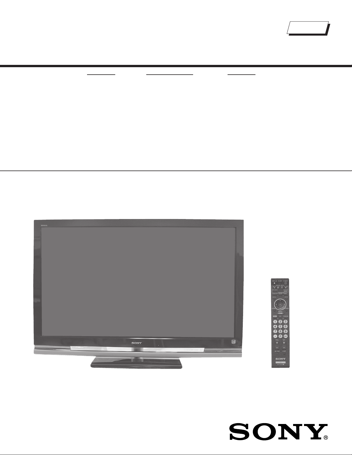
Sony KLV-52V410A, KLV-52W410A Service Manual

HISTORY INFORMATION FOR THE FOLLOWING MANUAL:
SERVICE MANUAL
MODEL NAME REMOTE COMMANDER DESTINATION
KLV-52V410A
KLV-52W410A
RM-YD023 BRAZIL
RM-YD023 BRAZIL
EX1
CHASSIS
ORIGINAL MANUAL ISSUE DATE: 6/2008
REVISION DATE SUBJECT
62008 No revisions or updates are applicable at this time.
LCD COLOR TELEVISION
9-883-793-01
Self Diagnosis
Supported model
SERVICE MANUAL
MODEL NAME REMOTE COMMANDER DESTINATION
KLV-52V410A
KLV-52W410A
RM-YD023 BRAZIL
RM-YD023 BRAZIL
EX1
CHASSIS
9-883-793-01
KLV-52W410A RM-YD023
LCD COLOR TELEVISION

KLV-52V410A/52W410A
TABLE OF CONTENTS
SECTION TITLE PAGE SECTION TITLE PAGE
Specifi cations ................................................................................. 4
Warnings and Cautions .................................................................. 6
Safety-Related Component Warning .............................................. 7
Safety Check-Out ........................................................................... 9
Self-Diagnostic Function ............................................................... 10
SECTION 1: DISASSEMBLY ............................................................... 12
1-1. Rear Cover Removal ............................................................ 12
1-2. Switch Unit Removal (Contains H1 Board) .......................... 12
1-3. Side Jack Bracket, BU Shield and BU Board Removal ........
1-4. G5 Board (Power Unit) and D4Z Board, and D5 Board
Removal .............................................................................. 13
1-5. Table-Top Stand and Under Cover Removal ........................ 14
1-6. AC Inlet Removal ................................................................. 14
1-7. Structural Frames and Brackets Removal ........................... 15
1-8. Speakers, Under Bar, H3E Board,
H4 Board, and Light Guide Removal ................................... 16
1-9. LCD Panel Removal ............................................................. 17
1-9-1. Cleaning the LCD Panel .......................................... 17
1-10. Balancer (ETC-Inverter MT) Board Removal ....................... 18
SECTION 2: SERVICE ADJUSTMENTS ............................................. 19
2-1. Viewing Service Adjustment Data ........................................ 19
2-2. Accessing Service Adjustment Mode ................................... 19
2-3. Viewing the Service Menus .................................................. 19
2-4. Using the Remote Commander to View Service Data ......... 20
2-5. Resetting to Factory Defaults ............................................... 20
13
SECTION 3: DIAGRAMS ..................................................................... 21
3-1. Circuit Boards Location ........................................................ 21
3-2. Printed Wiring Boards and
Schematic Diagrams Information ......................................... 21
3-3. Block Diagram ...................................................................... 23
3-4. Schematics and Supporting Information .............................. 24
BU Board Schematic Diagram (1 of 12) ............................... 24
BU Board Schematic Diagram (2 of 12) ............................... 25
BU Board Schematic Diagram (3 of 12) ............................... 26
BU Board Schematic Diagram (4 of 12) ............................... 27
BU Board Schematic Diagram (5 of 12) ............................... 28
BU Board Schematic Diagram (6 of 12) ............................... 29
BU Board Schematic Diagram (7 of 12) ............................... 30
BU Board Schematic Diagram (8 of 12) ............................... 31
BU Board Schematic Diagram (9 of 12) ............................... 32
BU Board Schematic Diagram (10 of 12) ............................. 33
BU Board Schematic Diagram (11 of 12) ............................. 34
BU Board Schematic Diagram (12 of 12) ............................. 35
D4Z Board Schematic Diagram ........................................... 37
D5 Board Schematic Diagram .............................................. 39
G5 Board Schematic Diagram ............................................. 41
H3E Board Schematic Diagram ........................................... 44
H4 Board Schematic Diagram .............................................. 46
3-5. Semiconductors ................................................................... 48
SECTION 4: EXPLODED VIEWS ........................................................ 49
4-1. Rear Cover Assembly and Table-Top Stand Assembly ....... 49
4-2. Chassis ................................................................................ 50
4-3. Connectors ........................................................................... 51
4-4. Bezel Assembly and LCD Panel ......................................... 52
4-5. Screw Legend ...................................................................... 53
KLV-52V410A/52W410A
SECTION 5: ELECTRICAL PARTS LIST ............................................ 54
APPENDIX A: ENCRYPTION KEY COMPONENTS ..........................A-1
3

SPECIFICATIONS
KLV-52V410A/52W410A
Power Requirements
Power Consumption (W)
In Use (Max)
In Standby
110V- 220V CA, 50/60Hz
285W (KLV-52V410A Only)
295W (KLV-52W410A Only)
Less than 0.1W
VIDEO (IN) 1/2/3:
S Video (4-Pin Mini DIN (VIDEO 1 Only)
Y: 1.0 Vp-p, 75 ohms unbalanced, sync negative
C: 0.286 Vp-p (Burst signal), 75 ohms
Video
1.0 Vp-p, 75 ohms unbalanced, sync negative
Audio
500 mVrms (Typical)
Impedance:47 kilohms
COMPONENT IN 1/2:
YP
Y:1.0 Vp-p, 75 ohms unbalanced, sync negative
PB:0.7 Vp-p, 75 ohms
PR:0.7 Vp-p, 75 ohms
Signal format: 480i, 480p, 576i, 576p, 720p, 1080i, 1080p
AUDIO
500 mVrms (Typical)
Impedance: 47 kilohms
(Component Video)
BPR
HDMI IN 1/2/3/4:
HDMI: Video: 480i, 480p, 576i, 576p, 720p, 1080i,1080p, 1080/24p
Audio: Two channel linear PCM 32, 44.1 and
48 kHz, 16, 20 and 24 bits, Dolby Digital
AUDIO (for HDMI IN 4 only):
500 mVrms (Typical)
Impedance: 47 kilohms
AUDIO OUT:
500 mVrms (Typical)
DIGITAL OUT (OPTICAL):
PCM/Dolby Digital optical signal
PC IN:
D-sub 15-pin, analog RGB, 0.7 Vp-p, 75 ohms, positive
PC AUDIO INPUT:
Stereo mini jack, 500 mVrms (Typical)
Impedance: 47 kilohms
KLV-52V410A/52W410A
Trademark Information
Blu-ray Disc is a trademark.
“BRAVIA” and , S-Force,
BRAVIA Sync, , DMe
trademarks or registered marks of Sony
Corporation.
x
and “x.v. Color” are
“XMB” and “XrossMediaBar” are the
trademarks of Sony Corporation and Sony
Computer Entertainment Inc.
“PLAYSTATION” is a registered trademark
and “PS3” is a trademark of Sony Computer
Entertainment Inc.
Adobe is a registered trademark or a trademark
of Adobe Systems Incorporated in United
States and/or other countries.
Macintosh is a trademark of Apple Inc.,
registered in the U.S. and other countries.
HDMI, the HDMI logo and High-Definition
Multimedia Interface are trademarks or
registered trademarks of HDMI Licensing,
LLC.
Manufactured under license from Dolby
Laboratories. “Dolby” and double-D symbol
are trademarks of Dolby Laboratories.
Design and specifi cations are subject to change without notice.
4
KLV-52V410
A
KLV-52W410A
Speaker Output
mm 65 X 150 mm
Dimensions (W x H x D)
with stand
mm 1,262 x 871 x 347 mm
without stand
mm 1,262 x 829 x 119 mm
wall-mount hole pattern 300 x 300 mm
wall-mount screw size
Mass
with stand
kg 38 kg
without stand
kg 32 kg
All measurements are approximations.
KLV-52V410A/52W410A
10W+10W
M6 x 12-18
Television system
NTSC PAL-M/PAL-N
Channel coverage
VHF: 2-13
UHF: 14-69
CATV: 1-125
Antenna
75-ohm external terminal for RF inputs
Panel System
LCD (Liquid Crystal Display) Panel
Display Resolution (horizontal x vertical)
1,920 dots x 1,080 lines
Screen Size (measured diagonally)
~ 132 cm (52 inches)
Supplied Accessories
Remote Commander RM-YD023
Two Size AA (R6) Batteries
AC Power Cord
Cable Holder (1 attached to the TV)
Operating Instructions
Quick Setup Guide
Warranty Card
Attaching the Table-Top Stand
Optional Accessories
Connecting Cables
Suport Belt Kit
DMX-DT1
KLV-52V410A/52W410A
5

KLV-52V410A/52W410A
WARNINGS AND CAUTIONS
CAUTION
These servicing instructions are for use by qualifi ed service personnel only. To reduce the risk of electric shock, do not perform any servicing other
than that contained in the operating instructions unless you are qualifi ed to do so.
CARRYING THE TV
Be sure to follow these guidelines to protect your
property and avoid causing serious injury.
• Before carrying the TV, disconnect all cables.
• Carrying the large size TV requires two or more
people.
• When carrying the TV, place your hand as
illustrated and hold it securely. Do not subject the
TV to shocks, vibration, or excessive force.
• Lift the TV by placing your palm directly
underneath the panel but do not:
• squeeze the speaker grill area
• place your fingers in the groove above the
speaker grill area
• put stress on the LCD panel.
• Do not lift the TV from the bottom center.
WARNING!!
An isolation transformer should be used during any service to avoid possible shock hazard, because of live chassis. The chassis of this receiver is
directly connected to the ac power line.
! SAFETY-RELATED COMPONENT WARNING!!
Components identifi ed by shading and ! mark on the schematic diagrams, exploded views, and in the parts list are critical for safe operation. Replace
these components with Sony parts whose part numbers appear as shown in this manual or in supplements published by Sony. Circuit adjustments that
are critical for safe operation are identifi ed in this manual. Follow these procedures whenever critical components are replaced or improper operation is
suspected.
KLV-52V410A/52W410A
6
SAFETY-RELATED COMPONENT WARNING
KLV-52V410A/52W410A
There are critical components used in LCD color TVs that are important for safety. These components are identifi ed with shading and
mark on the schematic diagrams and the electrical parts list. It is essential that these critical parts be replaced only with the part number
specifi ed in the electrical parts list to prevent electric shock, fi re, or other hazard.
NOTE: Do not modify the original design without obtaining written permission from the manufacturer or you will void the original parts and
labor guarantee.
!
USE CAUTION WHEN HANDLING THE LCD PANEL
When repairing the LCD panel, be sure you are grounded by using a wrist band.
When installing the LCD panel on a wall, the LCD panel must be secured using the 4 mounting holes on the rear cover.
To avoid damaging the LCD panel:
do not press on the panel or frame edge to avoid the risk of electric shock.
do not scratch or press on the panel with any sharp objects.
do not leave the module in high temperatures or in areas of high humidity for an extended period of time.
do not expose the LCD panel to direct sunlight.
avoid contact with water. It may cause a short circuit within the module.
disconnect the AC adapter when replacing the backlight (CCFL) or inverter circuit.
(High voltage occurs at the inverter circuit at 650Vrms.)
always clean the LCD panel with a soft cloth material.
use care when handling the wires or connectors of the inverter circuit. Damaging the wires may cause a short.
protect the panel from ESD to avoid damaging the electronic circuit (C-MOS).
LEAKAGE CURRENT HOT CHECK CIRCUIT
KLV-52V410A/52W410A
7
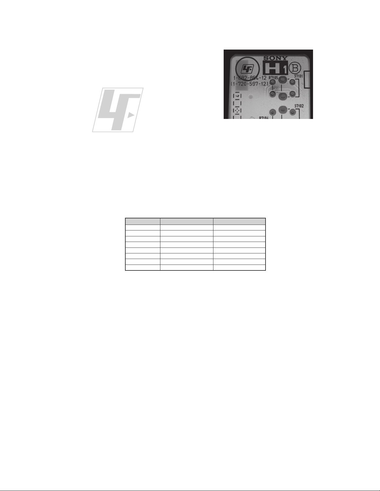
The circuit boards used in these models have been processed using
Lead Free Solder. The boards are identified by the LF logo located
close to the board designation e.g. H1 etc [ see example ]. The
servicing of these boards requires special precautions to be taken as
outlined below.
KLV-52V410A/52W410A
example 1
It is strongly recommended to use Lead Free Solder material in order to guarantee optimal quality of new solder joints.
Lead Free Solder is available under the following part numbers :
rebmuntraP retemaiD skrameR
91-500-046-7mm3.0gK52.0
02-500-046-7mm4.0gK05.0
12-500-046-7mm5.0gK05.0
22-500-046-7mm6.0gK52.0
32-500-046-7mm8.0gK00.1
42-500-046-7mm0.1gK00.1
52-500-046-7mm2.1gK00.1
62-500-046-7mm6.1gK00.1
Due to the higher melting point of Lead Free Solder the soldering iron tip temperature needs to be set to 370 degrees centigrade.
This requires soldering equipment capable of accurate temperature control coupled with a good heat recovery characteristics.
For more information on the use of Lead Free Solder, please refer to
http://www.sony-training.com
KLV-52V410A/52W410A
8
SAFETY CHECK-OUT
KLV-52V410A/52W410A
After correcting the original service problem, perform the following
safety checks before releasing the set to the customer:
1. Check the area of your repair for unsoldered or poorly soldered
connections. Check the entire board surface for solder splashes and
bridges.
2. Check the interboard wiring to ensure that no wires are “pinched” or
touching high-wattage resistors.
3. Check that all control knobs, shields, covers, ground straps, and
mounting hardware have been replaced. Be absolutely certain that
you have replaced all the insulators.
4. Look for unauthorized replacement parts, particularly transistors,
that were installed during a previous repair. Point them out to the
customer and recommend their replacement.
5. Look for parts which, though functioning, show obvious signs of
deterioration. Point them out to the customer and recommend their
replacement.
6. Check the line cords for cracks and abrasion. Recommend the
replacement of any such line cord to the customer.
7. Check the antenna terminals, metal trim, “metallized” knobs, screws,
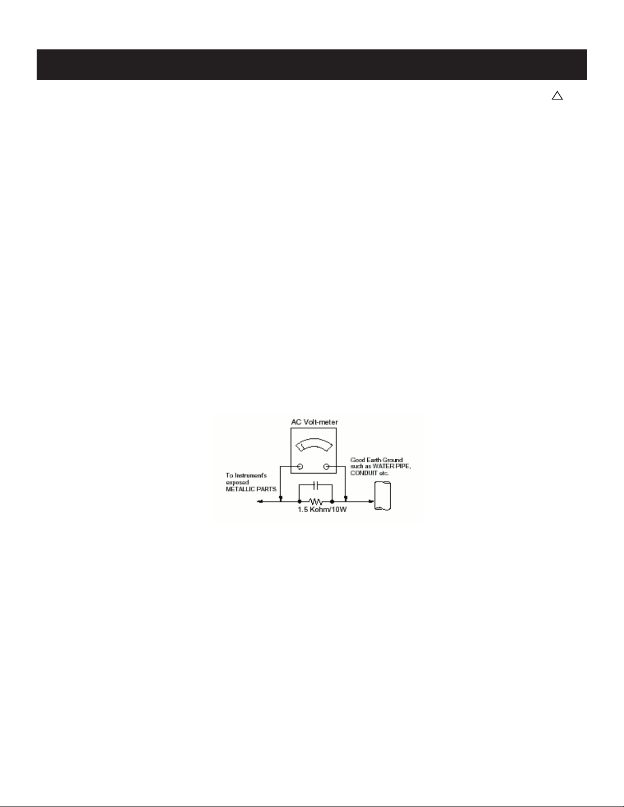
and all other exposed metal parts for AC leakage. Check leakage as
described below.
The AC leakage from any exposed metal part to earth ground and
from all exposed metal parts to any exposed metal part having a
return to chassis, must not exceed 0.5 mA (500 microamperes).
Leakage current can be measured by any one of three methods.
1. A commercial leakage tester, such as the Simpson 229 or RCA
WT-540A. Follow the manufacturers’ instructions to use these
instructions.
2. A battery-operated AC milliampmeter. The Data Precision 245
digital multimeter is suitable for this job.
3. Measuring the voltage drop across a resistor by means of a VOM
or battery-operated AC voltmeter. The “limit” indication is 0.75
V, so analog meters must have an accurate low voltage scale.
The Simpson’s 250 and Sanwa SH-63TRD are examples of
passive VOMs that are suitable. Nearly all battery-operated digital
multimeters that have a 2 VAC range are suitable (see Figure A).
How to Find a Good Earth Ground
A cold-water pipe is a guaranteed earth ground; the cover-plate
retaining screw on most AC outlet boxes is also at earth ground. If the
retaining screw is to be used as your earth ground, verify that it is at
ground by measuring the resistance between it and a cold-water pipe
with an ohmmeter. The reading should be zero ohms.
If a cold-water pipe is not accessible, connect a 60- to 100-watt
trouble- light (not a neon lamp) between the hot side of the receptacle
and the retaining screw. Try both slots, if necessary, to locate the hot
side on the line; the lamp should light at normal brilliance if the screw
is at ground potential (see Figure B).
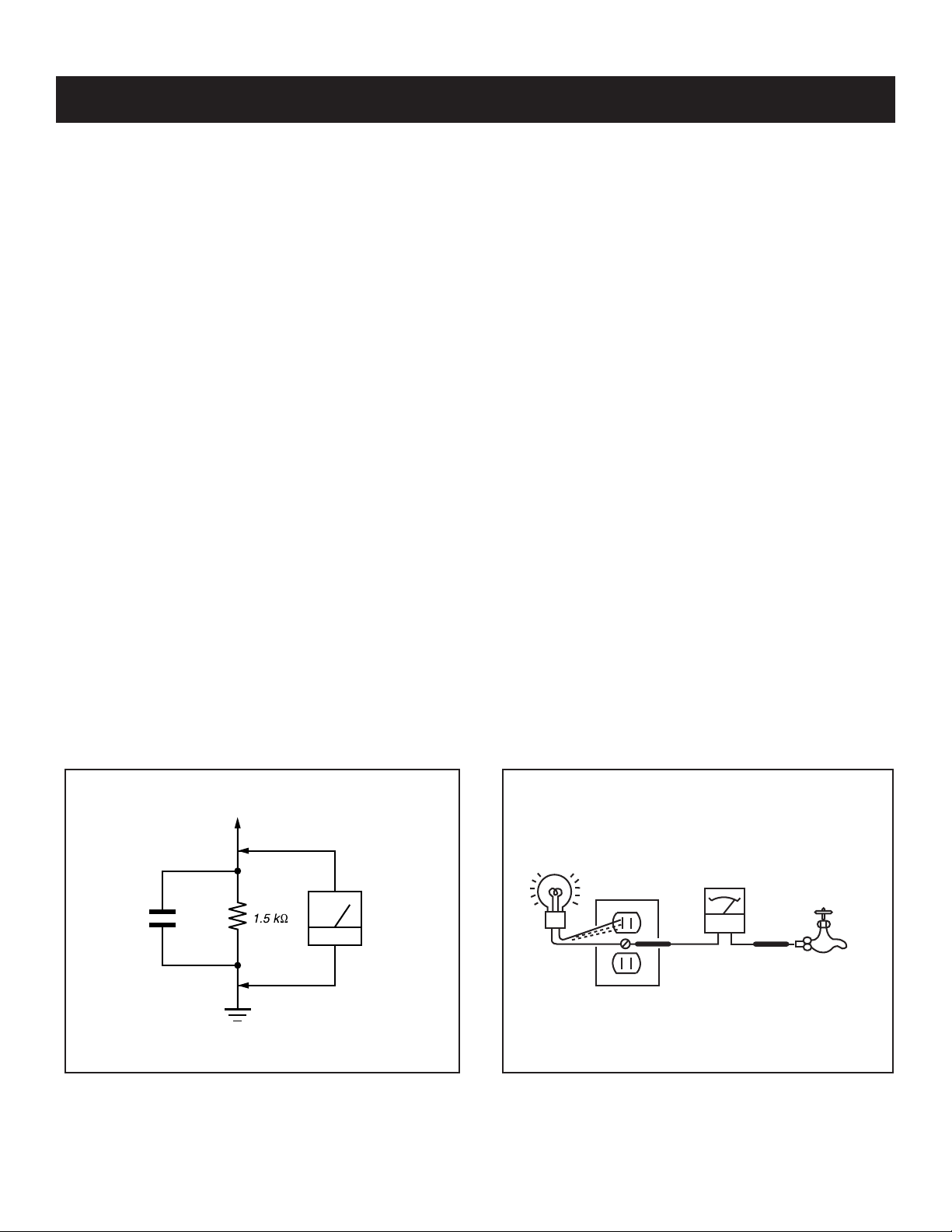
Leakage Test
0.15 μF
Figure A. Using an AC voltmeter to check AC leakage. Figure B. Checking for earth ground.
To Exposed Metal
Parts on Set
Earth Ground
AC
Voltmeter
(0.75V)
Trouble Light
AC Outlet Box
Ohmmeter
Cold-water Pipe
KLV-52V410A/52W410A
9
KLV-52V410A/52W410A
SELF-DIAGNOSTIC FUNCTION
The units in this manual contain a self-diagnostic function. If an error occurs, the STANDBY LED indicator will automatically begin to fl ash. The number
of times the LED fl ashes translates to a probable source of the problem. A defi nition of the STANDBY LED fl ash indicators is listed in the instruction
manual for the user’s knowledge and reference. If an error symptom cannot be reproduced, the Remote Commander can be used to review the failure
occurrence data stored in memory to reveal past problems and how often these problems occur.
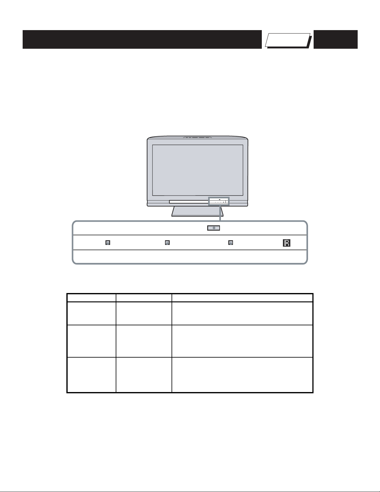
1. Diagnostic Test Indicators
When an error occurs, the STANDBY LED indicator will fl ash a set number of times to indicate the possible cause of the problem. If there is more than
one error, the indicator will identify the fi rst of the problem areas.
Control Buttons
Self Diagnosis
Supported model
Description of LED Indictors
LED LED Type Description
POWER LED
STANDBY LED
PIC OFF/
TIMER
LED
PIC OFF/TIMER STANDBY PO WE
Green LED
Red LED
* Light when the TV set is on
* Lights up in red when TV is in PC standby mode.
* If LED blinks continuously, this may indicate
that the TV needs servicing.
Green or Orange
LED
* Lights up in green when Picture Off is activated
* Lights up in orange when the timer is set
When timer is set, the LED remains lit even
when the TV is turned off.
R
KLV-52V410A/52W410A
10

KLV-52V410A/52W410A
2 times
5 times
LED ON 0.3 sec.
LED OFF 0.3 sec.
Viewing the Self Check Diagnostic List
1. TV must be in standby mode. (Power off).
2. Press the following buttons on the Remote Commander within a second of each other:
DISPLAY
The Self Check list displays. This differs from accessing Service Adjustments.
Results for all of the following diagnostic items are displayed on screen. No error has occurred if the screen displays a “0”.
Channel 5 Volume -
POWER
LED OFF
3 sec.
.
NOTE: If the Self Check display text is not completely visible, press the Menu
button on the Remote Commander to refresh the display.
HOME
SELF CHECK PAGE 1
002 MAIN_POWER 01
003 DC_ALERT1 00
Í 1 indicates an error was detected
Í 0 indicates no error was detected
005 PANEL_ALERT 00
006 BACKLIGHT 00
013 BACKLIGHT_BALANCE 00
00001 00027 00009 00000
3. Press the Channel 1 button on the Remote Commander to go to Page 2 of the Self Check list.
SELF CHECK PAGE 2
007 TEMP 00
008 SP_PROT 00
011 TRIDENT_IC 00
012 HFR_ERROR 00
012 TCON_ERROR 00
00001 00027 00009 00000
4. Press the Channel 4 button on the Remote Commander to go back to Page 1 of the Self Check list.
5. To exit Self Check display, turn the power off.
Clearing the Self Check Diagnostic List
1. In Service Mode, press the Channel 8 Channel 0.
KLV-52V410A/52W410A
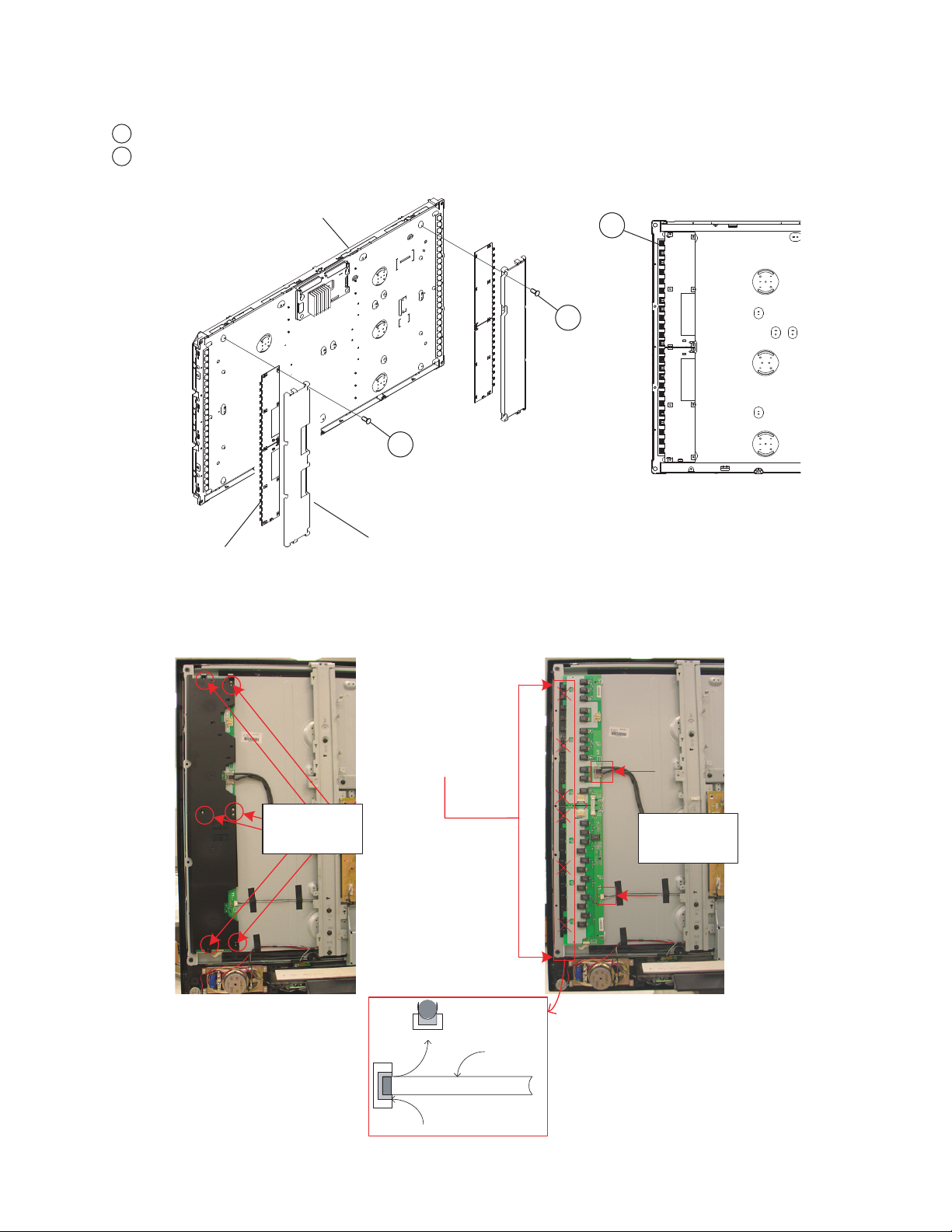
11

1-1. REAR COVER REMOVAL
1
Remove 2 screws from Terminal Position
2
Remove 6 screws
3
Remove 21 screws
KLV-52V410A/52W410A
SECTION 1: DISASSEMBLY
Rear Cover
1
3
1-2. SWITCH UNIT REMOVAL (CONTAINS H1 BOARD)
1
Remove Switch Unit from bezel (Contains H1 Board)
2
Disconnect 1 connector
Switch Unit
1
2
2
Bezel
KLV-52V410A/52W410A
12
1-3. SIDE JACK BRACKET, BU SHIELD AND BU BOARD REMOVAL
1
Release hook and slide out Side Jack Bracket from BU Board
2
Remove 2 HEX screws
3
Disconnect 5 connectors
4
Remove 9 screws
Main Bracket
1
BU Board
Side Jack Bracket
BU Shield
2
KLV-52V410A/52W410A
4
3
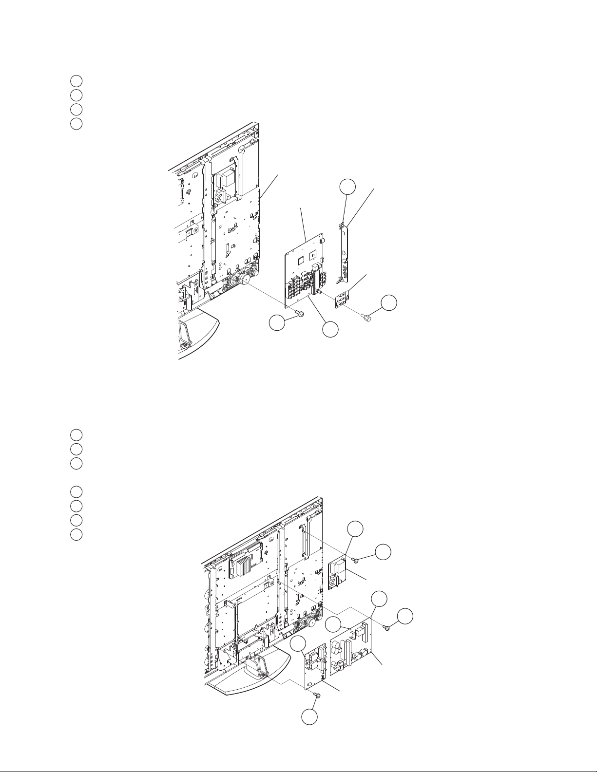
1-4. G5 BOARD (POWER UNIT) AND D4Z BOARD, AND D5 BOARD REMOVAL
1
Disconnect 3 connectors
2
Remove 4 screws
3
Disconnect 6 connectors (KLV-52V410A ONLY)
Disconnect 7 connectors (KLV-52W410A ONLY)
4
Remove 6 screws
5
Release 5 Board Holders
6
Disconnect 5 connectors
7
Remove 4 screws
1
2
D5 Board
3
KLV-52V410A/52W410A
5
4
6
G5 Board (Power Unit)
D4Z Board
7
13

1-5. TABLE-TOP STAND AND UNDER COVER REMOVAL
1
Remove 4 screws
2
Remove 1 screw
Under Cover
1
KLV-52V410A/52W410A
Table-Top Stand Assembly
2
1-6. AC INLET REMOVAL
1
Remove 2 screws
2
Remove 1 screw
AC Bracket
2
AC Inlet
1
Bottom Bracket
KLV-52V410A/52W410A
14
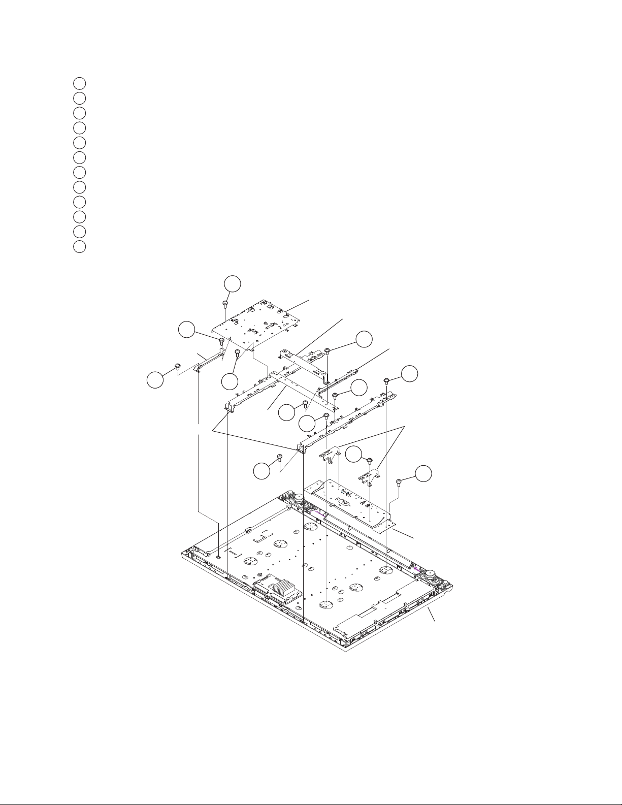
1-7. STRUCTURAL FRAMES AND BRACKETS REMOVAL
1
Remove 1 screw from D5 Support and LCD Panel
2
Remove 1 screw from D5 Support Frame
3
Remove 1 screw from Main Bracket and Bezel
4
Remove 3 screws from Main Bracket and Spine frame
5
Remove 2 screws from Top Vesa Bracket
6
Remove 2 screws from G5 Board Support
7
Remove 2 screws from Center Frame
8
Remove 2 screws from Spine Frames and Bottom Bracket
9
Remove 8 screws from Spine Frames
10
Remove 2 screws from Spine Frames and Bezel
11
Remove 4 screws from both Bottom Vesa Brackets
12
Remove 4 screws from Bottom Bracket
3
Main Bracket
Top Vesa Bracket
2
D5 Support
Frame
5
KLV-52V410A/52W410A
G5 Board Suport
1
Spine Frame
4
Center
Frame
10
8
7
6
9
11
Bottom Vesa Bracket
12
Bottom Bracket
Bezel
KLV-52V410A/52W410A
15

KLV-52V410A/52W410A
1-8. SPEAKERS, UNDER BAR, H3E BOARD, H4 BOARD, AND LIGHT GUIDE REMOVAL
1
Slide out Speaker (L) unit from Bezel
2
Slide out Speaker (R) unit from Bezel
3
Remove 2 screws from Under Bar
4
Disconnect 1 connector and Slide out H3E Board from Clear Panel
5
Release hooks and remove from Bezel
6
Remove 1 screw and Release hooks from Clear Panel
7
Disconnect 1 connector and Slide out H4 Board from Light Guide
8
Disconnect 1 connector and
Remove Illumination Module from Bezel. (KLV-52W410A ONLY)
3
Under Bar
1
4
H3E Board
Speaker Unit (L)
6
7
8
Illumination
Module
Bezel
5
Clear Panel
Light Guide
2
Speaker Unit (R)
KLV-52V410A/52W410A
16

1-9. LCD PANEL REMOVAL
NOTE: The LVDS cable can only be installed one way. There is colored tape on the cable to determine which side is attached
to the TCON and which side is attached to the BU Board.
1
Disconnect 3 connectors
2
Remove 2 screws
KLV-52V410A/52W410A
1
2
LCD Panel
Bezel
1-9-1. CLEANING THE LCD PANEL
CAUTION: When cleaning the TV, be sure to unplug the power cord to avoid any chance of electric shock.
1
Clean the cabinet of the TV with a dry soft cloth.
2
Wipe the LCD screen gently with a soft cloth.
Stubborn stains may be removed with a cloth slightly moistened with a solution of mild soap and warm water.
If using a chemically pretreated cloth, please follow the instruction provided on the package.
Never use strong solvents such as a thinner, alcohol or benzine for cleaning.
Periodic vacuuming of the ventilation openings is recommended to ensure to proper ventilation.
KLV-52V410A/52W410A
17
1-10. BALANCER (ETC-INVERTER MT) BOARD REMOVAL
1
Remove 7 screws from each Inverter Cover
2
Pull out the Balancer board from the Lamp Socket.
KLV-52V410A/52W410A
Balancer Board
LCD Panel
2
1
1
Cover
REMOVE SCREWS
SECURING
SHIELD
SHIELD REMOVAL
WARNING
NEVER REMOVE THE
SCREWS SECURING THE
PLASTIC STRIP HOLDING
THE LAMP SOCKETS
DAMAGE TO THE
BACKLIGHT TUBES WILL
OCC UR!
END VIEW
SOCKET
!
.
BACKLIGHT
REMOVE
CONNECTORS AND
PULL BOARDS TO
THE RIGHT
BALANCER (ETC-INVERTER) BOARD REMOVAL
Only remove the screws securing the inverter
cover which may be metal or plastic. The
remaining plastic strip contains sockets for the
fluorescent backlights and should never be
loosened. The backlights will pop out of the
sockets and/or break the backlight requiring a
LCD panel replacement.
KLV-52V410A/52W410A
18
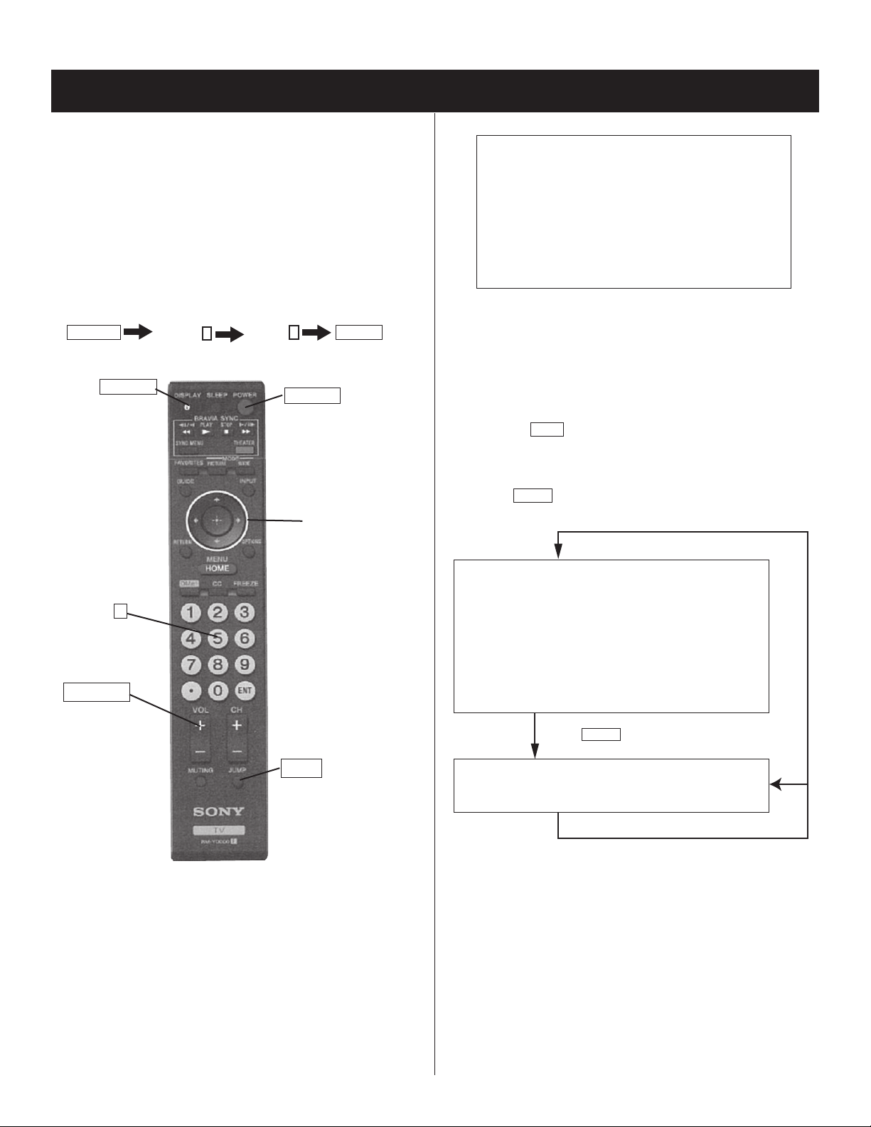
SECTION 2: SERVICE ADJUSTMENTS
2-1. VIEWING SERVICE ADJUSTMENT DATA
There are no adjustments necessary for these models. All data has
been set for optimal viewing for our customers. The following sections
are for informational purposes only.
2-2. ACCESSING SERVICE ADJUSTMENT
MODE
1. TV must be in standby mode. (Power off).
2. Press the following buttons on the Remote Commander within a
second of each other:
DISPLAY
Channel 5 Volume +
DISPLAY
POWER
POWER
.
KLV-52V410A/52W410A
TVLF CHECK
001 COLOR ADJ
001 R_DRV
DIGITAL PROGRAM
DATA
BE PROGRAM
NVM
PACK
BOOT
Sample TV Service Menu
SERVICE
00100
: H801.03 0070
: S001000
: TM1.000
: TD1.000
: TP1.000
: TB1.000
2-3. VIEWING THE SERVICE MENUS
Use the Remote Commander to view the BE and Digital service menus
options.
1. To display the Service Menu that contains the Category you want to
adjust, press
(For a complete list of the service Categories refer to Service Menus)
JUMP
on the Remote Commander.
5
VOLUME+
RM-YD023
Onscreen cursor
and select button
JUMP
NOTE: If the Service Menu display text is not completely visible, press
the Menu
display.
TVLF CHECK
001 COLOR ADJ
001 R_DRV
DIGITAL PROGRAM
DATA
BE PROGRAM
NVM
PACK
BOOT
QM 0 0
INFO
button on the Remote Commander to refresh the
HOME
SERVICE
00100
: H801.03 0070
: S001000
: TM1.000
: TD1.000
: TP1.000
: TB1.000
Press JUMP
SERVICE
DTV
Sample Service Menus
The fi rst service menu (TV) displays.
KLV-52V410A/52W410A
19

2-4. USING THE REMOTE COMMANDER TO
VIEW SERVICE DATA
Use the buttons on the Remote Commander to access the service menu
items and adjust the data values.
1. Access Service Mode.
Press the following buttons on the Remote Commander within a
second of each other:
DISPLAY
Category
Number
Adjustment
Item Number
The screen displays the fi rst category in the selected service menu.
NOTE: If the Service Menu display text is not completely visible,
press the Menu
the display.
2. To change the category, press 2 or 5 on the Remote Commander.
Note: Pressing 2 or 5 only changes the categories within the service
menu displayed.
To change a category on one of the other service menus, press the
JUMP
3. To change the adjustment item, press 1 or 4 on the Remote
Commander.
4. To exit service mode, turn the power off.
Channel 5 Volume +
POWER
Adjustment
Category
TVLF CHECK
001 COLOR ADJ
001 R_DRV
DIGITAL PROGRAM
DATA
BE PROGRAM
NVM
PACK
BOOT
button on the Remote Commander to refresh
HOME
Item
SERVICE
00100
: H801.03 0070
: S001000
: TM1.000
: TD1.000
: TP1.000
: TB1.000
Data Value
button until the correct service menu is displayed.
.
Next item
Read data
from last
saved NVM
2-5. RESETTING TO FACTORY DEFAULTS
Previous
item
1
4
0
MUTING
Write into
memory
RM-YD023
KLV-52V410A/52W410A
POWER
2
Next
Category
Previous
5
Category
8
Restore User Control
and Channel Memory
ENT
JUMP
Displays
Service
Menus
Use the following instructions to restore the User Controls and
Channel Memory settings to the preset factory conditions.
1. While holding down the
on the Remote Commander, press the
POWER button on the Front Panel of the set.
The set restarts and displays the initial setup screen. This may take
several minutes.
KLV-52V410A/52W410A
20

3-1. CIRCUIT BOARDS LOCATION
KLV-52V410A/52W410A
SECTION 3: DIAGRAMS
D5
SWITCH UNIT (CONTAINS H1)
G5
BU
D4Z
ILLUMINATION
MODULE
(KLV-52W410A ONLY)
H4
H3E
3-2.
PRINTED WIRING BOARDS AND SCHEMATIC DIAGRAMS INFORMATION
All capacitors are in μF unless otherwise noted. pF : μμF 50WV or
less are not indicated except for electrolytics and tantalums.
All electrolytics are in 50V unless otherwise specifi ed.
All resistors are in ohms. kΩ=1000Ω, MΩ=1000kΩ
Indication of resistance, which does not have one for rating
electrical power, is as follows: Pitch : 5mm
Rating electrical power :
1
/
W in resistance, 1/
4
W and 1/
10
W in chip resistance.
16
1
/
4
: nonfl ammable resistor
All voltages are in V.
S : Measurement impossibility.
: B+line.
: B-line. (Actual measured value may be different).
: signal path. (RF)
Circled numbers are waveform references.
W
The components identifi ed by shading and ! symbol are critical for safety. Replace
only with part number specifi ed.
: fusible resistor
: internal component
The symbol indicates a fast operating fuse and is displayed on the component
side of the board. Replace only with fuse of the same rating as marked.
: panel designation and adjustment for repair
: earth ground
: earth-chassis
All variable and adjustable resistors have characteristic curve B,
unless otherwise noted.
NOTE: The components identifi ed by a red outline and a mark contain confi dential
information. Specifi c instructions must be adhered to whenever these components
are repaired and/or replaced.
See Appendix A: Encryption Key Components in the back of this manual.
Readings are taken with a color-bar signal input.
Readings are taken with a 10MΩ digital multimeter.
Voltages are DC with respect to ground unless otherwise noted.
Voltage variations may be noted due to normal production
tolerances.
KLV-52V410A/52W410A
21
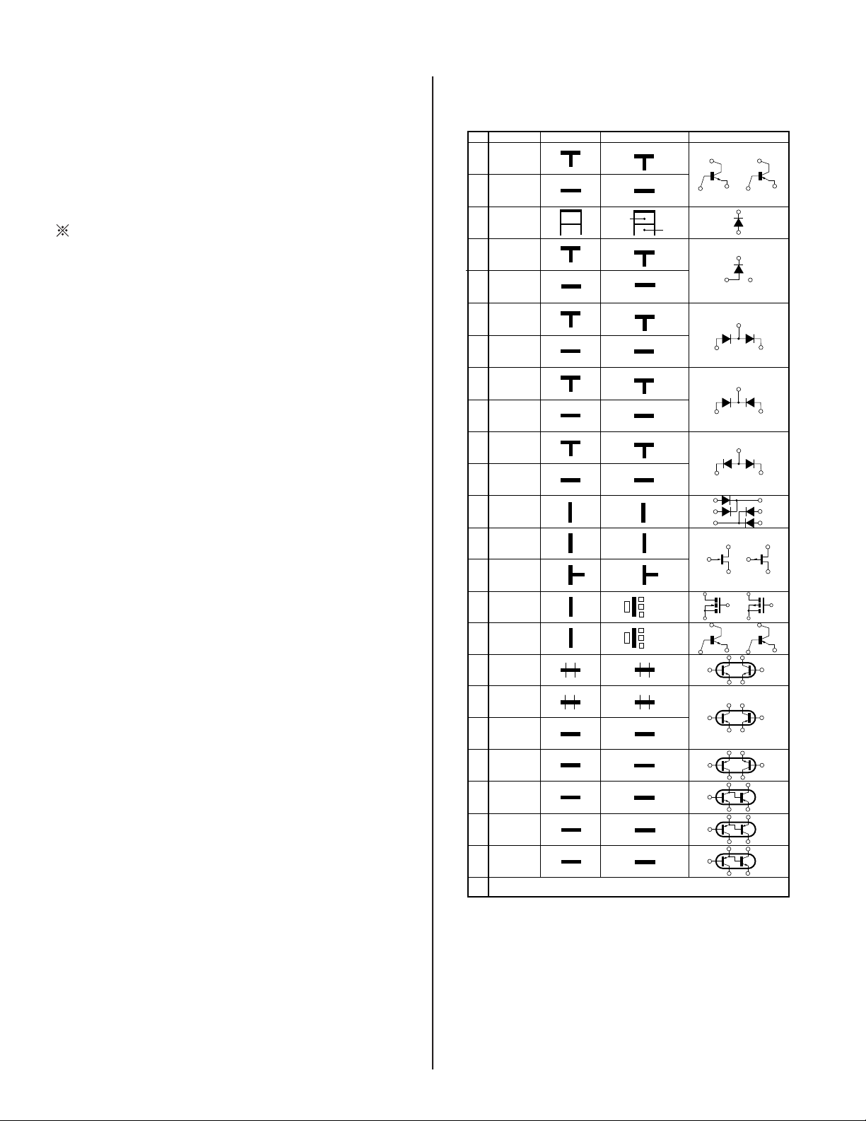
KLV-52V410A/52W410A
REFERENCE INFORMATION
RESISTOR
: RN METAL FILM
: RC SOLID
: FPRD NONFLAMMABLE CARBON
: FUSE NONFLAMMABLE FUSIBLE
: RW NONFLAMMABLE WIREWOUND
: RS NONFLAMMABLE METAL OXIDE
: RB NONFLAMMABLE CEMENT
: ADJUSTMENT RESISTOR
COIL
: LF-8L MICRO INDUCTOR
CAPACITOR
: TA TANTALUM
: PS STYROL
: PP POLYPROPYLENE
: PT MYLAR
: MPS METALIZED POLYESTER
: MPP METALIZED POLYPROPYLENE
: ALB BIPOLAR
: ALT HIGH TEMPERATURE
: ALR HIGH RIPPLE
Terminal name of semiconductors in silk screen
printed circuit ( )
Device Printed symbol Terminal name
Transistor
1
Transistor
2
3
Diode
4
Diode
Diode
5
Diode
6
Diode
7
8
Diode
Diode
9
Diode
0
Diode
!¡
Diode
!™
Transistor
!£
(FET)
Transistor
!¢
(FET)
Transistor
!?
(FET)
Transistor
!§
Transistor
!¶
Transistor
!•
Transistor
!ª
Transistor
@º
Transistor
@¡
Transistor
@™
Transistor
@£
Discrete semiconductot
–
(Chip semiconductors that are not actually used are included.)
*
Collector
Base
Collector
Base
Cathode
Cathode
Anode
Cathode
Anode
Common
Anode
Common
Anode Cathode
Common
Anode
Common
Anode Anode
Common
Cathode
Common
Cathode
Anode
Anode
Cathode
Drain
Drain
B1 E1
C2
B2 C1E2
B2 E2
C1
B1 C2
E1
B2 E2
C1
B1 C2E1
B2 E2
C1
B1 C2E1
E2
B1 E1
C2
(B2)
E1
B1
C1
(B2)
E1
E2
C2
Emitter
Emitter
Anode
(NC)
(NC)
Cathode
Anode
Cathode
Cathode
Cathode
Anode
Anode
Source
Gate
Source
Gate
Source
Drain
Gate
Emitter
Collector
Base
C1(B2)
E2
C2
B1
C1
Circuit
D
G
D
S
B1
B1
B1
B1
B1
B1
D
G
S
S
D
G
C1
E1
C1
E1
E1
C1
E2
C1
C1
G
S
C2
B2
E2
C2
B2
E2
E2
B2
C2
C2C1(B2)
E2
E2E1(B2)
C2
C2E1(B2)
C2
Ver.1.6
KLV-52V410A/52W410A
22
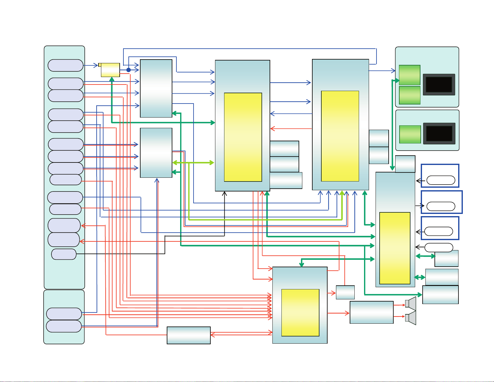
3-3. BLOCK DIAGRAM
㱍
KLV-52V410A/52W410A
Rear Inputs
RF
S + Video1
Video3
Component1
Component2
HDMI1
HDMI3
HDMI4
Audio
for DVI
PC (HD15)
Audio
for PC
Audio out
(Var./Fix)
Optical
Audio Out
USB1.1
Side Inputs
Video2
HDMI2
Tu.
Tu.
Video SW
Video SW
CXA2241
CXA2241
( 90h )
( 90h )
HDMI
HDMI
EQ_SW
EQ_SW
AD8197
AD8197
to 1
44to 1
( 9Eh )
( 9Eh )
for ATSC
CVBS for PAP
for Slicer
DDC
Audio
Compound IC
IIC
YOUT for Slicer
x245
x245
CPU
Demod.
MPEG2 Dec.
3D GPX
CC/PL
Sub Chroma
EPG(Gemstar)
USB
Ether
SPDIF
Digital Video
ITU-R BT.656
ITU-R BT.1120
Digital GPX
RGB
HV Sync/CLK
One NAND
One NAND
64MB
64MB
DDR2
DDR2
64MB
64MB
EEPROM
EEPROM
8kB ( A0h )
8kB ( A0h )
CVBS
YUV
YUV
TMDS
RGB
IIC
IIS
CXD9926TP
H/V/CLK
for GPX
IIS(HDMI)
IIC
CXD9926TP
( 68h )
( 68h )
Audio SW
ADC
DSP
Surround
DAC
CXD9937GB
CXD9937GB
ADC
3D Comb.
Chroma Dec.
IPC
HDMI Rx
ME/MC
YC Process
Scalar
RGB Process
PIP Process
GPX Mix
LVDS Tx
8bit bus
UART
SPDIF
for UI
sound
ADC
ADC
Audio Amp.
TPA3100D2
LVDS
DDR2
DDR2
32MB
32MB
DDR2
DDR2
32MB
32MB
IIC
Flash
Flash
2MB
2MB
BE Micro
MB91305
[Control]
Trident
ATI
Video SW
HDMI SW
Power
TAS
HFR
CEC
Audio Mute
HFR
FHD
( 18h )
T-Con
FHD
T-Con
FHD
FHD Panel
with HFR
LCD
FHD
FHD Panel
LCD
FHD
H1 board
Buttons
H3E board
LEDs
H4 board
SIRCS
ECS
IIC
EEPROM
EEPROM
32kB ( A0h )
32kB ( A0h )
IIC
Temperature
Temperature
Sensor
Sensor
( 92h )
( 92h )
RTC
RTC
( 64h )
( 64h )
KLV-52V410A/52W410A
23

3-4. SCHEMATICS AND SUPPORTING INFORMATION
BU BOARD SCHEMATIC DIAGRAM (1 OF 12)
1 | 2 | 3 | 4 | 5 | 6 | 7 | 8 | 9 | 10 | 11 | 12 | 13 | 14 | 15 | 16 | 17 | 18 | 19 | 20 | 21 | 22 | 23 | 24
KLV-52V410A/52W410A
A
—
B
—
C
—
D
—
E
—
F
—
G
—
H
—
I
VideoInput1
VideoInput3
VideoInput2
J1051
D3.3V
A_V1_IN_C,A_V1_IN_S2SW,A_V1_IN_SSW,A_V1_IN_V,A_V1_IN_Y
A_V1_IN_Y
R1021
75
C1052
6.3V
X6S
1005
C1053
6.3V
X6S
1005
1/10W
RN-CP
0.5%
VD1004
R1007
1/16W
CHIP
VD1005
R1009
1/16W
CHIP
R1011
1/16W
CHIP
GND
R1005
1M
1/16W
CHIP
1M
1M
1M
R1004
75
1/10W
RN-CP
VD1002
C1001
1
10V
X7R
1608
GND
R1023
75
1/10W
RN-CP
0.5%
C1002
1
R1025
1/10W
RN-CP
0.5%
6.3V
X6S
1005
C1003
1
6.3V
X6S
1005
75
C1004
1
6.3V
X6S
1005
C1005
1
6.3V
X6S
1005
R1006
2.2k
1/16W
CHIP
5%
R1008
2.2k
1/16W
CHIP
5%
GND
R1010
2.2k
1/16W
CHIP
5%
R1012
2.2k
1/16W
CHIP
5%
A_V1_IN_C
A_V1_IN_S2SW
Opt/Audio Output
A_V1_IN_SSW
A_V1_IN_V
A_V_IN
V1_IN_L
V1_IN_R
A_V3_IN_V
PC_LR IN
V3_IN_L
V3_IN_R
AMEM & XBR = 1-821-899-11
SYMBOL/MACRONOT READY
AUDIO IN
A_V2_IN_V
1
V2_IN_L
V2_IN_R
1
A_V_IN
VD1001
GND
6
34
3
4
12
12
5
V1
9
V1_DET
10
7
8
L1
11
12
R1
13
15
14
V2
18
V3_DET
19
16
17
GND
L2
20
21
R2
22
24
23
*J1001
VD1006
V
GND
L
R
4
3
VD1052
12
4
3
12
GND
VD1051
GND
VD1007
R1053
1/16W
CHIP
1005
R1055
1M
1/16W
CHIP
5%
1005
D3.3V
1M
5%
GND
4
3
12
R1051
10k
1/16W
CHIP
5%
GND
R1054
2.2k
1/16W
CHIP
5%
1005
R1056
2.2k
1/16W
CHIP
5%
1005
R1052
100
1/16W
CHIP
5%
1005
VD1003
GND
V2_DET
R1057
75
1/10W
RN-CP
0.5%
*J1201
7P
VIN
VCC
GND
*J1202
*J1203
*J1204
L
R
VD1203
L
R
1
2
3
4
4
12
GND
D3.3V
VD1205
C1204
0.1
16V
1005
VD1201
GND
3
4
12
GND
4
3
12
GND
3
R1205
1/16W
CHIP
Q1401
RT3N77M-TP-1
7
5
10k
RB1401
2143658
1
4
2
6
3
R1415
GND
2.2k
1/16W
R1416
100
1/16W
C1403
10V
X7R
2012
4.7
C1405
0.01
25V
X7R
1005
MAZ8039G0LS0
AU_13V
D1410
STBY3.3V
R1418
330k
1/16W
RN-CP
0.5%
AC_OFF_DET
POWER1
JL1410
JL1411
214
X7R
25V
0.01
C1401
3
REG12V
GND
1005CHIP
1005CHIP
1608CHIP
600
FB1401
1
3
5
7
2
4
6
8
R1413
CHIP
2012
600
FB1402
FB1403
0uH
0
R1410
R1411
R1412
0
0
0
REG12V
JL1407
2
4
6
8
C1411
0.001
50V
X7R
1005
JL1403
1
3
5
7
JL1406
JL1401
JL1402
GND_AU
JL1404
GND
JL1405
CL1401
BAL_ERR(42_CMO-INV)
1
GND
2
INV_ERR
3
BACKLIGHTON/OFF
4
DIMMER
5
HEATER_ON
6
REG12V
7
CN1401
POWERON
1
AC OFF DET
2
STBY 3.3V
3
UNREG13V
4
UNREG13V
5
UNREG13V_GND
6
UNREG13V_GND
7
REG12V_GND
8
REG12V_GND
9
REG12V_GND
10
REG12V
11
REG12V
12
REG12V
13
CN1411
WHT
TO PWRBOARD
CN6154
7P
TO PWRBOARD
CN6150
13P
A_LINEOUT
A_SPDIF_OUT
GND TERMINAL
E
ET1001
E
ET1002
E
ET1003
E
1005
R1420
330k
1/16W
CHIP
5%
E
E
E
E
E
MAZ8150G0LS0
R1421
1/16W
1005
CHIP
C1421
0.1
16V
1005
ET1004
ET1005
ET1006
ET1007
ET1008
ET1009
D1421
33k
5%
Q1424
UNR52A1G0LS0
GND
TPC8109(TE12L)
Q1423
S1 S2 S3 G
4321
D1D2D3D4
R1208
1/16W
CHIP
R1206
2.2k
1/16W
CHIP
2.2k
C1212
0.001
50V
X7R
1005
C1215
0.001
50V
X7R
1005
R1202
220k
1/16W
CHIP
5%
1005
R1204
220k
1/16W
CHIP
1005
5%
A_LINEOUT_L
A_LINEOUT_R
C1213
C1214
GND
6.3V
X6S
1005
6.3V
X6S
1005
F1422
POWER3
GND
5A
C1420
24V
1
25V
X7R
2012
1
PC_IN_L
PC_IN_R
1
C1210
1
6.3V
X6S
1005
DVI_IN_L
DVI_IN_R
C1211
1
6.3V
X6S
1005
A_PC_IN
REG12V
A_DVI_IN
HP_DET
R1201
2.2k
1/16W
CHIP
5%
R1203
2.2k
1/16W
CHIP
5%
1M
5%
R1207
1M
R1212
2.2k
1/16W
CHIP
R1211
1M
R1215
2.2k
1/16W
CHIP
R1214
1M
1/16W
CHIP
5%
BALANCER_ERR
8765
INVERTER_ERR
BACKLIGHT
DIMMER_DRV_OUT
PANEL12V
—
J
—
K
—
L
—
M
—
N
—
O
—
P
ComponentInput1
ComponentInput2
*J1101
GND
D1_IN_CB,D1_IN_CR,D1_IN_Y
D1_IN_Y
D1_IN_CB
D1_IN_CR
C1101
6.3V
X6S
1005
C1102
6.3V
X6S
1005
C1103
6.3V
X6S
1005
C1104
6.3V
X6S
1005
R1115
75
1/10W
RN-CP
0.5%
1
D1_IN_L
D1_IN_R
1
D2_IN_Y
D2_IN_CB
D2_IN_CR
R1121
75
1/10W
RN-CP
0.5%
1
D2_IN_L
D2_IN_R
1
A_D_IN
VSW_OUT_Y/CV
VSW_OUT_C,VSW_OUT_Y/CV
VSW_OUT_C
D2_IN_CB,D2_IN_CR,D2_IN_Y
A_ATI_GRA_V
A_ATI_CC_VY
A_D_IN
GND
R1113
1/10W
RN-CP
0.5%
R1119
1/10W
RN-CP
0.5%
75
75
75
75
R1102
2.2k
1/16W
CHIP
1005
R1104
2.2k
1/16W
CHIP
1005
R1106
2.2k
1/16W
CHIP
1005
R1108
2.2k
1/16W
CHIP
1005
5%
5%
5%
5%
R1111
1/10W
RN-CP
0.5%
R1117
1/10W
RN-CP
0.5%
G1
BL1
R1
L1
R2
G2
BL2
R3
L2
R4
D1_DET
VD1101 VD1102 VD1103
R1101
1M
1/16W
CHIP
1005
R1103
1M
1/16W
CHIP
4
3
1005
D2_DET
GND
VD1104
12
GND
VD1121 VD1122 VD1123
GND
4
3
VD1124
12
GND
R1105
1/16W
CHIP
1005
R1107
1M
1/16W
CHIP
1005
1M
REG5V
FB1301
0uH
C1310
16V
47
GND
RT3S02M-T111-1
Q1301
47 680
321
47
RT3S02M-T111-1
Q1302
47 680
321
47
RT3S02M-T111-1
Q1303
47 680
321
47
RT3S02M-T111-1
Q1304
47 680
321
47
C1309
0.1
25V
X7R
1608
654
DC1.0V / 1VppOUT
654
DC1.8V
2VppOUT
654
sub-Display
Graphics
R1314
1k
1/16W
RN-CP
0.5%
654
2VppOUT
AMD-CC
R1316
1k
1/16W
RN-CP
0.5%
R1313
1/16W
RN-CP
0.5%
1k
R1315
1/16W
RN-CP
0.5%
Analog Tu
A_480I_Y
C1307
1
25V
2012
X7R
R1307
100
1/16W
CHIP
21 22 23 24 25 26 27 28 29 30
NC
S2_4
IN5_C
CV/YOUT1
20
COUT1
19
NC
18
CV/YOUT2
17
COUT2
16
NC
15
CVOUT3
14
CV/YOUT3
13
COUT3
12
DCOUT
11
GND
1k
IN5_Y
CXA2241Q-T4
VideoSW
IN1_CV
NC
NC
GND
1005CHIP
C1308
X7R
2012
R1308
1/16W
VCC
IC1301
90HEX
GND
1/16W
5%
R1301100
1
25V
100
S1_4
IN2_CV
201225V
X7R
TV_M_MON_V
IN5_CV
S1_1
R1317
100
1/16W
CHIP
5%
C13011
IIC
SCL_DEVICE
SDA_DEVICE
SCL
SDA
IN2_C
IN2_Y
A_V3_IN_V
ADR
IN4_C
IN4_Y
IN4_CV
IN3_C
IN3_Y
IN3_CV
S2_1
12345678910
1005CHIP
1005CHIP
1005CHIP
S2_3
S1_3
S2_2
S1_2
1/16W
1/16W
1/16W
31
32
33
1/16W
34
5%
35
R1305100
36
37
38
39
40
5%
R1302100
201225V
5%
X7R
R1303100
201225V
5%
X7R
R1304100
201225V
X7R
C13021
C13031
C13041
1005CHIP
201225V
X7R
R1306
100
1/16W
CHIP
5%
A_V1_IN_S2SW
A_V1_IN_C
A_V1_IN_Y
A_V1_IN_SSW
A_V1_IN_V
C1306
25V
X7R
2012
C13051
1
Video2
A_V2_IN_V
A_DMP_V
for DMPort-CV
Video3
A_V1_IN_C,A_V1_IN_S2SW,A_V1_IN_SSW,A_V1_IN_V,A_V1_IN_Y
Video1
1
3
GND
RB1302
100
RB1303
100
RB1304
100
C1223
1k
RB1307
10k
3
RB1306
214
2
4
RB1305
10k
10k
V1_DET
V3_DET
D1_DET
D2_DET
A_DMP_DET
PC_DET
BU 1/12
VIDEO SW & I/O
A-1506-055-A <EX1> BU-P1
KLV-52V410A/52W410A 24
 Loading...