

Sony klv23hr1 schematic

SERVICE MANUAL
SPECIFICATIONS
KLV-23HR1
US Model
Canadian Model
Television system:
American TV standard
Channel coverage:
VHF: 2-13/UHF: 14-69/CATV: 1-125
Antenna:
75 ohm external terminal for VHF/UHF
Screen size (measured diagonally):
23 inches
Panel System:
a-Si TFT Active Matrix LCD panel
(Effective dots: more than 99.99%)
Display resolution:
1280 dots (horizontal) x 768 lines (vertical)
VIDEO 1/2 IN:
S VIDEO IN (4-pin mini DIN):
Y: 1 Vp-p, 75-ohms unbalanced,
sync negative
C: 0.286 Vp-p (Burst signal),
75 ohms
VIDEO: 1 Vp-p, 75-ohms unbalanced,
sync negative
AUDIO: 500 mVrms (100% modulation)
Impedance: 47 kilohms
VIDEO 3 IN:
COMPONENT VIDEO (Y, PB, PR) IN:
Y: 1.0 Vp-p, 75 ohms
unbalanced, sync negative
B
: 0.7 Vp-p, 75 ohms
P
P
R
: 0.7 Vp-p, 75 ohms
Signal format:
480i, 480p, 720p, 1080i
AUDIO: 500 mVrms (100% modulation)
Impedance: 47 kilohms
AUDIO OUT:
500 mVrms (100% modulation)
More than 500 mVrms at the maximum volume setting
(Variable)
More than 500 mVrms (Fixed)
Headphones:
Stereo minijack
Impedance: 16 ohms
Speaker:
55 mm (2 1/4 inches) dome woofer (2)
17 mm (
Speaker output:
4 W x 2, 12 ohms
11
/16 inches) dome tweeter (2)
LCD Colour TV

Power requirement:
120 V AC, 60 Hz
DC input:
14.5 V DC
Power consumption:
In use (Max.): 88 W
In standby: 1.2 W
Dimensions (W/H/D):
Including TV stand: 601 x 497 x 184 mm
3
(23
/4 x 19 5/8 x 7 1/4 inches)
Without TV stand: 601 x 433 x 91 mm
3
/4 x 17 1/8 x 3 5/8 inches)
(23
Mass:
Including TV stand: 9.0 kg (19 lb 13 oz)
Without TV stand: 7.8 kg (17 lb 3 oz)
Supplied accessories:
Remote control RM-928Y (1)
Batteries size AA (2)
75-ohm coaxial cable (1)
AC power cord (1)
AC power adaptor AC-FD002 (1)
Operating Instructions
Warranty Card
Optional accessorios:
Note that some optional accessories may be out of
stock.
Headphones plug adaptor
Connecting cables
VMC-810S/820S, YC-15V/30V,
RK-74A, VMC-10HG, SMF-403
Wall-Mount Bracket
SU-W200
Design and specifications are subject to change
without notice.
KLV-23HR1 (UC) 2
SAFETY CHECK-OUT
After correcting the original service problem, perform the
following safety checks before releasing the set to the customer:
1. Check the area of your repair for unsoldered or poorly-soldered connections. Check the entire board surface for solder
splashes and bridges.
2. Check the interboard wiring to ensure that no wires are
“pinched” or contact high-wattage resistors.
3. Check that all control knobs, shields, covers, ground straps,
and mounting hardware have been replaced. Be absolutely
certain that you have replaced all the insulators.
4. Look for unauthorized replacement parts, particularly transistors, that were installed during a previous repair. Point them
out to the customer and recommend their replacement.
5. Look for parts which, though functioning, show obvious signs
of deterioration. Point them out to the customer and recommend their replacement.
6. Check the line cords for cracks and abrasion. Recommend
the replacement of any such line cord to the customer.
7. Check the B+ and HV to see if they are specified values.
Make sure your instruments are accurate; be suspicious of
your HV meter if sets always have low HV.
8. Check the antenna terminals, metal trim, “metallized” knobs,
screws, and all other exposed metal parts for AC Leakage.
Check leakage as described right.
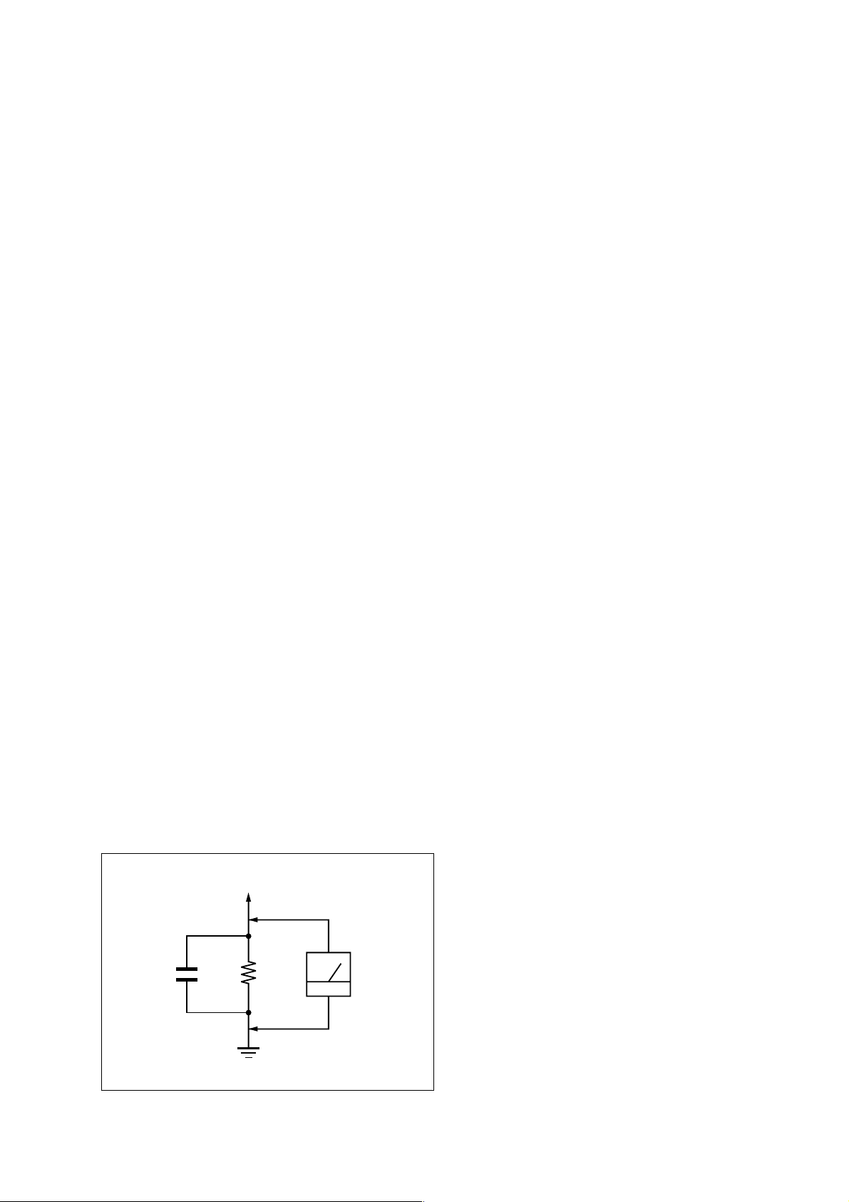
LEAKAGE TEST
The AC leakage from any exposed metal part to earth ground
and from all exposed metal parts to any exposed metal part
having a return to chassis, must not exceed 0.5 mA (500
microamperes).
Leakage current can be measured by any one of three methods.
1. A commercial leakage tester, such as the Simpson 229 or RCA
WT -540A. Follow the manuf acturers’ instructions to use these
instruments.
2. A battery-operated A C milliammeter . The Data Precision 245
digital multimeter is suitable for this job.
3. Measuring the voltage drop across a resistor by means of a
VOM or battery-operated AC voltmeter. The “limit” indication is 0.75 V, so analog meters must have an accurate lowvoltage scale. The Simpson 250 and Sanwa SH-63Trd are
examples of a passive V OMs that are suitable. Nearly all battery operated digital multimeters that have a 2 V AC range
are suitable. (See Fig. A)
WARNING!!
SAFETY-RELATED COMPONENT WARNING!!
COMPONENTS IDENTIFIED BY SHADING AND MARK
! ON THE SCHEMATIC DIAGRAMS, EXPLODED
VIEWS AND IN THE PARTS LIST ARE CRITICAL FOR
SAFE OPERATION. REPLACE THESE COMPONENTS
WITH SONY PARTS WHOSE PART NUMBERS APPEAR AS SHOWN IN THIS MANUAL OR IN SUPPLEMENTS PUBLISHED BY SONY. CIRCUIT ADJUSTMENTS THAT ARE CRITICAL FOR SAFE OPERATION
ARE IDENTIFIED IN THIS MANUAL. FOLLOW THESE
PROCEDURES WHENEVER CRITICAL COMPONENTS
ARE REPLACED OR IMPROPER OPERATION IS
SUSPECTED.
AVERTISSEMENT!!
ATTENTION AUX COMPOSANTS RELATIFS À LA
SÉCURITÉ!!
LES COMPOSANTS IDENTIFIÉS PAR UNE TRAME ET
UNE MARQUE ! SONT CRITIQUES POUR LA
SÉCURITÉ. NE LES REMPLACER QUE PAR UNE
PIÈCE PORTANT LE NUMÉRO SPECIFIÉ. LES
RÉGLAGES DE CIRCUIT DONT L’IMPORTANCE EST
CRITIQUE POUR LA SÉCURITÉ DU
FONCTIONNEMENT SONT IDENTIFIÉS DANS LE
PRÉSENT MANUEL. SUIVRE CES PROCÉDURES
LORS DE CHAQUE REMPLACEMENT DE
COMPOSANTS CRITIQUES, OU LORSQU’UN
MAUVAIS FONCTIONNEMENT EST SUSPECTÉ.
To Exposed Metal
Parts on Set
0.15 µF
1.5 k
Ω
Earth Ground
AC
Voltmeter
(0.75 V)
Fig. A. Using an AC voltmeter to check AC leakage.
KLV-20HR1(UC) 3

TABLE OF CONTENTS
1. DISASSEMBLY
1-1. Rear Panel Assy Removal ................................... 1-1
1-2. Stand Assy and Rear Cover Assy Removal ........ 1-1
1-3. H2 Board and Speaker Removal ......................... 1-2
1-4. U1 Board Removal .............................................. 1-2
1-5. TU Board Removal .............................................. 1-3
1-6. A, B2, and G Boards Removal ............................ 1-3
1-7. LCD Panel Removal ............................................ 1-4
1-8. H3 Board Removal .............................................. 1-4
1-9. H1 Board Removal .............................................. 1-5
2. ADJUSTMENTS .................................... 2-1
3. DIAGRAMS
3-1. Block Diagrams ....................................................3-1
3-2. Frame Diagram .....................................................3-6
3-3. Circuit Boards Location ....................................... 3-7
3-4. Schematic Diagrams and Printed Wiring Boards 3-7
(1) A Board .................................................................3-8
(2) B2 Board .............................................................3-14
(3) G Board ............................................................... 3-20
(4) H1, H2 and H3 Boards .......................................3-22
(5) TU Board ............................................................3-20
(6) U1 Board .............................................................3-22
3-5.Semiconductors ........................................................ 3-25
4. EXPLODED VIEWS
4-1. Chassis .................................................................4-2
4-2. Packing Materials ................................................ 4-3
5. ELECTRICAL PARTS LIST...................5-1
KLV-23HR1 (UC) 4
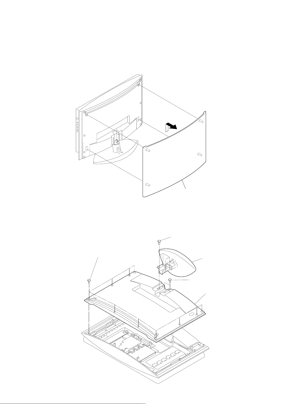
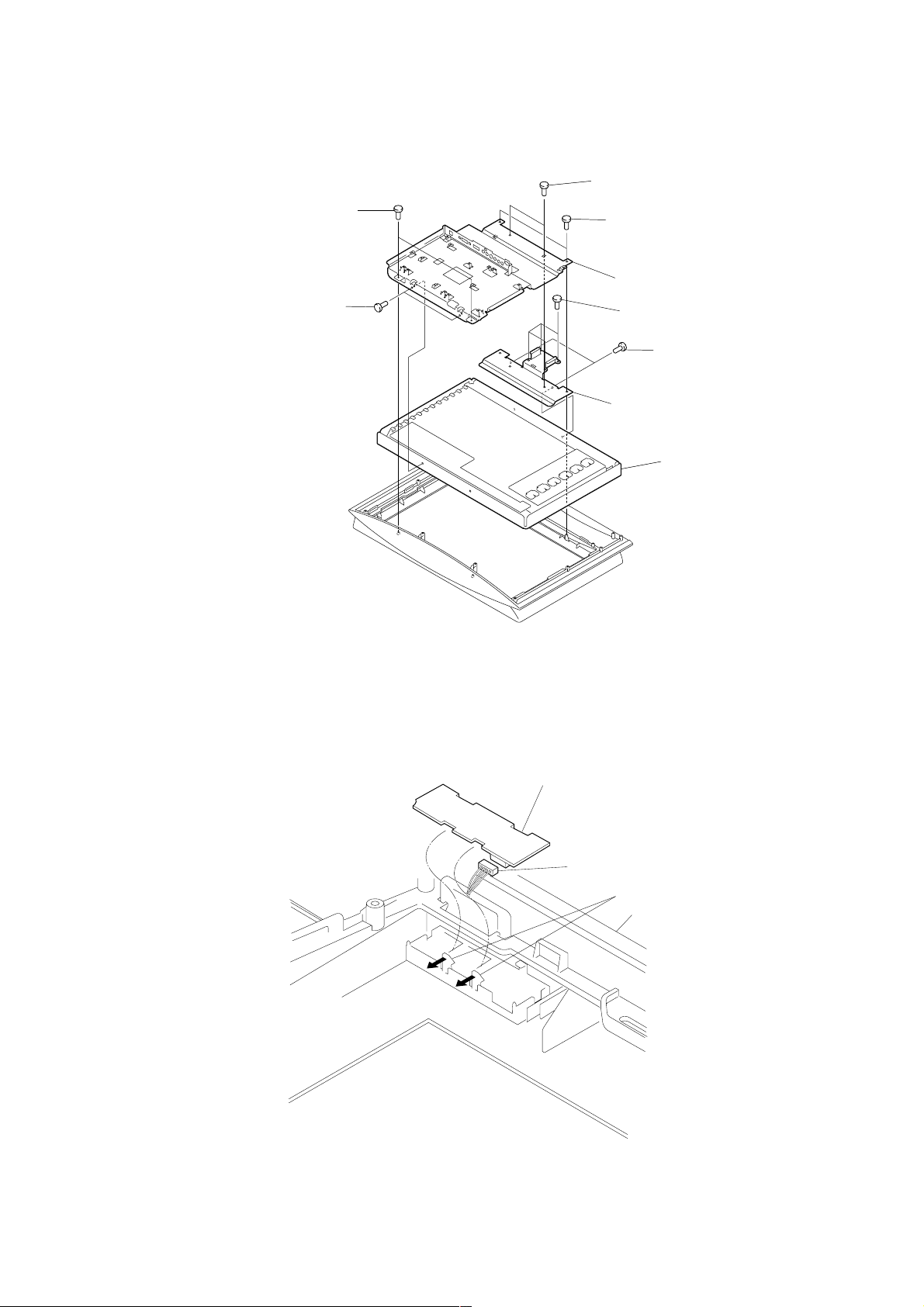
1-1. REAR PANEL ASSY REMOVAL
SECTION 1
DISASSEMBLY
1-2. STAND ASSY AND REAR COVER ASSY REMOVAL
1 Four screws
(+PS 4x12)
3 Ten screws
(+BVTP 3x10)
1 Rear panel assy
2 Stand assy
3Two screws
(+BVTP 3x10)
4 Rear cover
KLV-23HR1 (UC) 1-1
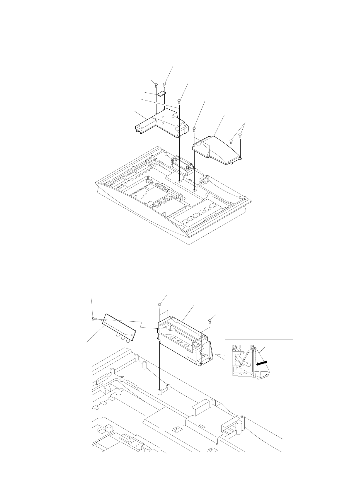
1-3. H2 BOARD AND SPEAKER REMOVAL
1 Screw
4 Screw
(+BVTP 3x10)
2 H2 board
5 Speaker(L)
(+BVTP 3x12)
3 Two screw
(+BVTT 3x6)
6 Two screw
(+BVTT 3x6)
8 Speaker(R)
7 Two screw
(+BVTP 3x10)
1-4. U1 BOARD REMOVAL
3 Two screws
(+BVTP 3x10)
5 U1 board
1 Twe screws
(+BVTP 3x10)
2 Front terminal block assy
1 Twe screws
(+BVTP 3x10)
Cover
4 Push
KLV-23HR1 (UC) 1-2
1-5. TU BOARD REMOVAL
1 Two screws
(+BVTT 3x6)
2 Tuner bracket
Cord
4 TU board
3 Nut, Washer
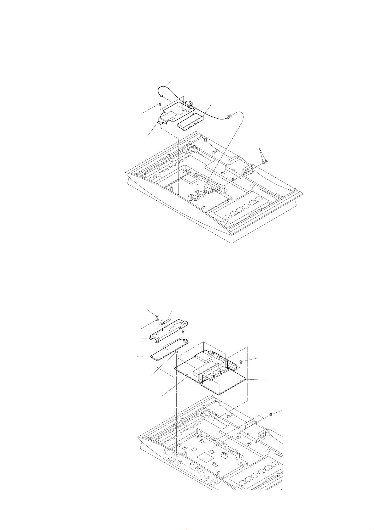
1-6. A, B2, AND G BOARDS REMOVAL
1 Two screws
(+BVTT 3x6)
2 Two mini guide spacer
3 Shield case G1
5 G board
6 Four screws
(+BVTT 3x6)
9 A board
Lead clamper
4 Three screws
(+BVTT 3x6)
7 Five screws
(+BVTT 3x6)
!º B2 board
8 Two screws
(+BVTP 3x10)
KLV-23HR1 (UC) 1-3
1-7. LCD PANEL REMOVAL
2 Two screws
(+BVTP 4x12)
3 Two screws
(+PSW 3x12)
1 Two screws
(+BVTT 3x6)
2 Two screws
(+BVTP 4x12)
4 LCD bracket assy
5 Four screws
(+BVTP 4x12)
6 Two screws
(+PSW 3x12)
7 Hinge supporter
8 LCD panel
1-8. H3 BOARD REMOVAL
2 H3 board
1 Connecter
CN1502
Two claw
Cabnet assy
KLV-23HR1 (UC) 1-4
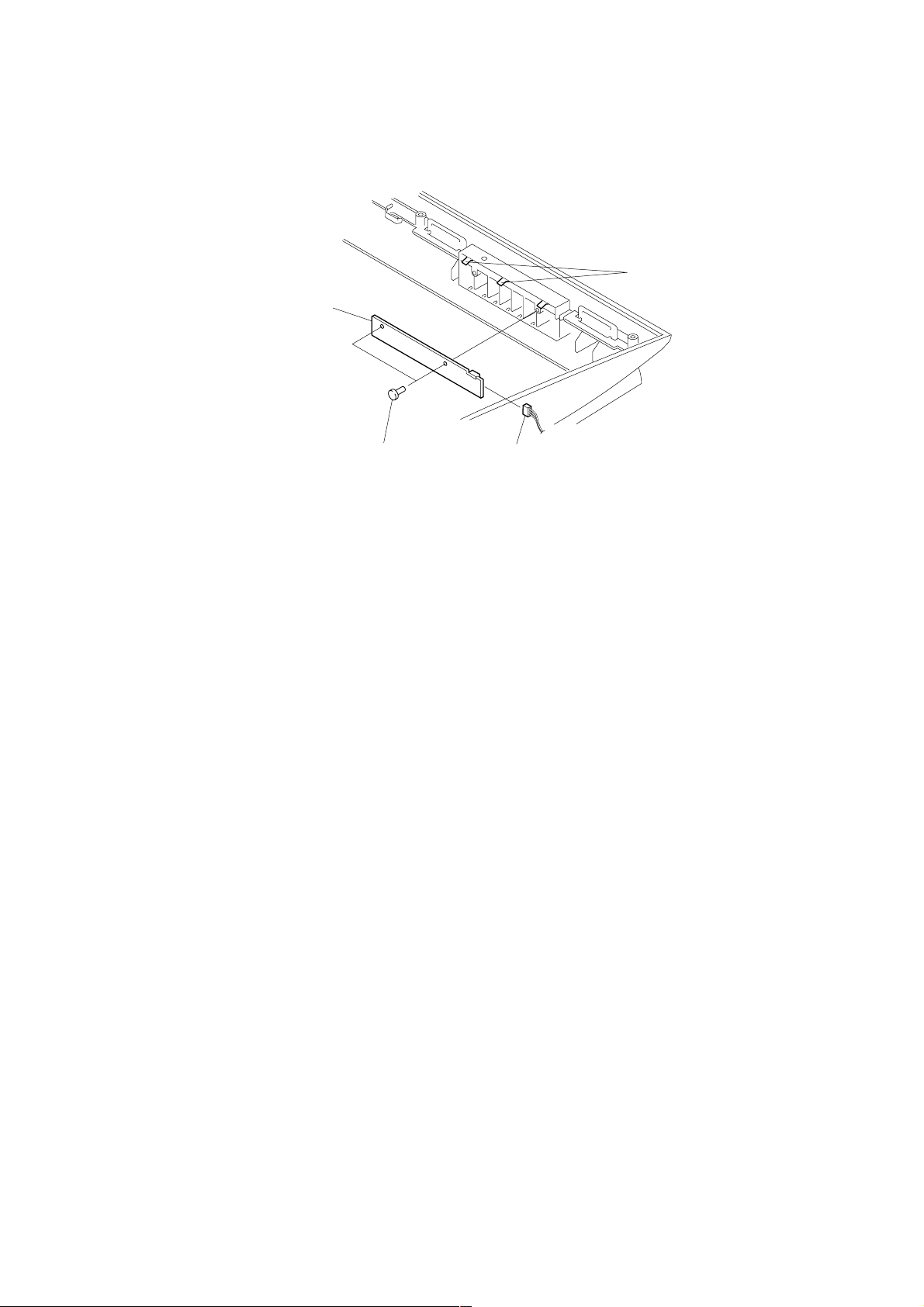
1-9. H1 BOARD REMOAVL
3 H1 board
Claw (three places)
1 Two screws
(+BVTP 3x10)
2 Connector
CN1501
KLV-23HR1 (UC) 1-5E
SECTION 2
ADJUSTMENTS
< PREPARATIONS >
1.Aging
•Input no signal and set the monitor to aging mode.
•Aging Setting
IMON_CON_REG_2 = 152
2. Aging condition
Applied voltage: Rated +10%
Interval of time: Over 10 min
Ambient temperature: 22dC to 28dC
Brightness: The value is set by aging mode
Note:
When the power is cycled between aging and W/B adjustment,
perform the aging in 30sec or more before the W/B adjustment.
2-1. AD calibration adjustment of TV/Video input
1. Check TIMING_INDEX=0 (Auto-detect mode).
2. Set the vgport_sel to 1 (YCbCr determination mode) of hardware register.
Caution: This item is set 0 automatically when powered on.
3. Input All black signal (0 IRE) with burst into the video (composite) input.
4. Check that the average value of the 2 registers is in above
value with 2 registers of
sony_input_r_ymin and sony_input_r_y_max from the ECS.
Reference Adjustment Adjustment
item condition register
sony_input_r_y_min+sony_input_r_y_max 16 ± 3 Not adjusted
2
5. Input All white signal (100 IRE) with burst.
6. Check that the average value of the 2 registers is in above
value with 2 registers of
sony_input_r_ymin and sony_input_r_y_max from the ECS.
Reference Adjustment Adjustment
item condition register
sony_input_r_y_min+sony_input_r_y_max 160 ± 5 Not adjusted
2 (CT)
Note:Video1 and Video2 has common setting
“TIMING_INDEX=2”.
2-2. AD calibration adjustment of component input
1. Set the vgport_sel to 1 (YCbCr determination mode) of hardware register.
Caution: This item is set 0 automatically when powered on.
2. Input All black signal (0 IRE) of [480i :D1] into the component input.
3. Check that the average value of the 2 registers is in above
value with 2 registers of
sony_input_r_ymin and sony_input_r_y_max from the ECS.
Reference Adjustment Adjustment
item condition register
sony_input_r_y_min+sony_input_r_y_max 16 ± 3 Not adjusted
2
4. Input All white signal (100 IRE) into the component input.
5. Adjust av erage v alue of the 2 registers to abo ve with reading 2
registers of sony_input_r_ymin and
sony_input_r_y_max from the ECS.
Reference Adjustment Adjustment
item condition register
sony_input_r_y_min+sony_input_r_y_max 160 ± 3 CIP CT
2
6. Repeat step 2 to 5 until the detection set value in step 2 and 4
above are obtained.
7. Perform the Service Save.
8. Copy the adjusted value of CIP_CT (step 2-5) in [480i :D1]
signal area of TIMING_INDEX=3.
9. Set the TIMING_INDEX to 0 (Auto-detect mode) and perform the Service Save.
2-3. AD calibration adjustment of [1080i :D3] input
1. Set the vgport_sel to 1 (YCbCr determination mode) of hardware register.
Caution: This item is set 0 automatically when powered on.
2. Input All black signal (0 IRE) of [1080i :D3] into the component input.
3. Adjust v alue of the AD_OFFSET_D3_Y as follo ws with reading 2 registers of sony_input_r_y_min
and sony_input_r_y_max from the ECS.
Reference Adjustment Adjustment
item condition register
sony_input_r_y_min+sony_input_r_y_max 16 ± 2
2
sony_input_r_y_min 16
sony_input_r_y_max 16
AD_OFFSET_D3_Y
-5
+0
-0
+5
KLV-23HR1 (UC) 2-1
4. Adjust v alue of the AD_OFFSET_D3_PR as f ollows with reading 2 registers of sony_input_g_cr_min
and sony_input_g_cr_max from the ECS.
Reference Adjustment Adjustment
item condition register
sony_input_g_cr_min+sony_input_g_cr_max 128 ± 1
2
sony_input_g_cr_min 128
sony_input_g_cr_max 128
5. Adjust v alue of the AD_OFFSET_D3_PB as f ollows with reading 2 registers of
sony_input_b_cb_min and sony_input_ b_cb _max from the
ECS.
Reference Adjustment Adjustment
item condition register
sony_input_b_cb_min+sony_input_b_cb_max 128 ± 1
2
sony_input_b_cb_min 128
sony_input_b_cb_max 128
6. Input All white l (100 IRE) of [1080i :D3] into the component
input.
7. Adjust v alue of the AD_GAIN_D3_Y as follows with reading
2 registers of sony_input_r_y_min and
sony_input_r_y_max from the ECS.
Reference Adjustment Adjustment
item condition register
sony_input_r_y_min+sony_input_r_y_max 178 ± 1
2
sony_input_r_y_min 178
sony_input_r_y_max 178
8. Input All red (50 IRE) of [1080i :D3] into the component input.
9. Adjust value of the AD_GAIN_D3_PR as follows with reading 2 registers of sony_input_g_cr_min
and sony_input_ g_cr _max from the ECS.
Reference Adjustment Adjustment
item condition register
sony_input_g_cr_min+sony_input_g_cr_max 230 ± 1
2
sony_input_g_cr_min 230
sony_input_g_cr_max 230
10. Input All blue (50 IRE) of [1080i :D3] into the component
input.
11. Adjust v alue of the AD_GAIN_D3_PB as follows with reading 2 registers of sony_input_b_cb_min
and sony_input_ b_cb _max from the ECS.
Reference Adjustment Adjustment
item condition register
sony_input_b_cb_min+sony_input_b_cb_max 230 ± 1
2
sony_input_b_cb_min 230
sony_input_b_cb_max 230
AD_OFFSET_D3_PR
-5
+
0
-0
+5
AD_OFFSET_D3_PB
-5
+
0
-0
+5
AD_OFFSET_D3_Y
-5
+
0
-0
+5
AD_OFFSET_D3_PR
-5
+
0
-0
+5
AD_OFFSET_D3_PB
-5
+
0
-0
+5
12 Repeat step 3-2 to 3-11 until the detection set value in step 3-
3 to 3-5, 3-7, 3-9 and 3-11 above are obtained.
13. Copy the adjusted value in register for [480p :D2] and [720p
:D4] .
AD_OFFSET_D2_Y AD_OFFSET_D3_Y
AD_OFFSET_D4_Y
AD_OFFSET_D2_PB AD_OFFSET_D3_ PB
AD_OFFSET_D4_ PB
AD_OFFSET_D2_PR AD_OFFSET_D3_ PR
AD_OFFSET_D4_ PR
AD_GAIN_D2_Y AD_ GAIN _D3_Y
AD_ GAIN_D4_Y
AD_ GAIN _D2_PB AD_ GAIN _D3_ PB
AD_ GAIN_D4_ PB
AD_ GAIN _D2_ PR AD_ GAIN _D3_ PR
AD_ GAIN _D4_ PR
14. Perform the Service Save.
2-4. AD calibration adjustment of [480p :D2] input
1. Set the vgport_sel to 1 (YCbCr determination mode) of hardware register.
Caution: This item is set 0 automatically when powered on.
2. Input All black signal (0 IRE) of [480p :D2] into the component input.
3. Adjust v alue of the AD_OFFSET_D2_Y as follo ws with reading 2 registers of sony_input_r_y_min
and sony_input_r_y_max from the ECS.
Reference Adjustment Adjustment
item condition register
sony_input_r_y_min+sony_input_r_y_max 16 ± 2
2
sony_input_r_y_min 16
sony_input_r_y_max 16
4. Adjust v alue of the AD_OFFSET_D2_PR as f ollows with reading 2 registers of sony_input_g_cr_min
and sony_input_g_cr_max from the ECS.
Reference Adjustment Adjustment
item condition register
sony_input_g_cr_min+sony_input_g_cr_max 128 ± 1
2
sony_input_g_cr_min 128
sony_input_g_cr_max 128
5. Adjust v alue of the AD_OFFSET_D2_PB as f ollows with reading 2 registers of
sony_input_b_cb_min and sony_input_ b_cb _max from the
ECS.
Reference Adjustment Adjustment
item condition register
sony_input_b_cb_min+sony_input_b_cb_max 128 ± 1
2
sony_input_b_cb_min 128
sony_input_b_cb_max 128
KLV-23HR1 (UC) 2-2
AD_OFFSET_D2_Y
-5
+0
-0
+5
AD_OFFSET_D2_PR
-5
+
0
-0
+5
AD_OFFSET_D2_PB
-5
+
0
-0
+5
6. Input All white l (100 IRE) of [480p :D2] into the component
input.
7. Adjust v alue of the AD_GAIN_D3_Y as follows with reading
2 registers of sony_input_r_y_min and
sony_input_r_y_max from the ECS.
Reference Adjustment Adjustment
item condition register
sony_input_r_y_min+sony_input_r_y_max 178 ± 1
2
sony_input_r_y_min 178
sony_input_r_y_max 178
8. Input All red (50 IRE) of [480p :D2] into the component input.
9. Adjust value of the AD_GAIN_D2_PR as follows with reading 2 registers of sony_input_g_cr_min
and sony_input_ g_cr _max from the ECS.
Reference Adjustment Adjustment
item condition register
sony_input_g_cr_min+sony_input_g_cr_max 230 ± 1
2
sony_input_g_cr_min 230
sony_input_g_cr_max 230
10. Input All blue (50 IRE) of [480p :D2] into the component
input.
11. Adjust v alue of the AD_GAIN_D2_PB as follows with reading 2 registers of sony_input_b_cb_min
and sony_input_ b_cb _max from the ECS.
Reference Adjustment Adjustment
item condition register
sony_input_b_cb_min+sony_input_b_cb_max 230 ± 1
2
sony_input_b_cb_min 230
sony_input_b_cb_max 230
12. Repeat step 2 to 11 until the detection set value in step 3 to 5,
7, 9 and 11 above are obtained.
13. Perform the Service Save.
AD_OFFSET_D2_Y
-5
+
0
-0
+5
AD_OFFSET_D2_PR
-5
+
0
-0
+5
AD_OFFSET_D2_PB
-5
+
0
-0
+5
2-5. AD calibration adjustment of [720 :D4] input
1. Set the vgport_sel to 1 (YCbCr determination mode) of hardware register.
Caution: This item is set 0 automatically when powered on.
2. Input All black signal (0 IRE) of [720p :D4] into the component input.
3. Adjust v alue of the AD_OFFSET_D4_Y as follo ws with reading 2 registers of sony_input_r_y_min
and sony_input_r_y_max from the ECS.
Reference Adjustment Adjustment
item condition register
sony_input_r_y_min+sony_input_r_y_max 16 ± 2
2
sony_input_r_y_min 16
sony_input_r_y_max 16
AD_OFFSET_D4_Y
-5
+0
-0
+5
4. Adjust v alue of the AD_OFFSET_D4_PR as f ollows with reading 2 registers of sony_input_g_cr_min
and sony_input_g_cr_max from the ECS.
Reference Adjustment Adjustment
item condition register
sony_input_g_cr_min+sony_input_g_cr_max 128 ± 1
2
sony_input_g_cr_min 128
sony_input_g_cr_max 128
5. Adjust v alue of the AD_OFFSET_D4_PB as f ollows with reading 2 registers of
sony_input_b_cb_min and sony_input_ b_cb _max from the
ECS.
Reference Adjustment Adjustment
item condition register
sony_input_b_cb_min+sony_input_b_cb_max 128 ± 1
2
sony_input_b_cb_min 128
sony_input_b_cb_max 128
6. Input All white l (100 IRE) of [720p :D4] into the component
input.
7. Adjust value of the AD_GAIN_D4_Y as follows with reading
2 registers of sony_input_r_y_min and
sony_input_r_y_max from the ECS.
Reference Adjustment Adjustment
item condition register
sony_input_r_y_min+sony_input_r_y_max 178 ± 2
2
sony_input_r_y_min 178
sony_input_r_y_max 178
8. Input All red (50 IRE) of [720p :D4] into the component input.
9. Adjust value of the AD_GAIN_D4_PR as follows with reading 2 registers of sony_input_g_cr_min
and sony_input_ g_cr _max from the ECS.
Reference Adjustment Adjustment
item condition register
sony_input_g_cr_min+sony_input_g_cr_max 230 ± 1
2
sony_input_g_cr_min 230
sony_input_g_cr_max 230
10. Input All blue (50 IRE) of [720p :D4] into the component
input.
AD_OFFSET_D4_PR
-5
+
0
-0
+5
AD_OFFSET_D4_PB
-5
+
0
-0
+5
AD_OFFSET_D4_Y
-5
+0
-0
+5
AD_OFFSET_D4_PR
-5
+
0
-0
+5
KLV-23HR1 (UC) 2-3
11. Adjust v alue of the AD_GAIN_D4_PB as follows with reading 2 registers of sony_input_b_cb_min
and sony_input_ b_cb _max from the ECS.
Reference Adjustment Adjustment
item condition register
sony_input_b_cb_min+sony_input_b_cb_max 230 ± 1
2
sony_input_b_cb_min 230
sony_input_b_cb_max 230
12. Repeat step 2 to 11 until the detection set value in step 3 to 5,
7, 9 and 11 above are obtained.
13. Perform the Service Save.
AD_OFFSET_D4_PB
-5
+
0
-0
+5
2-6. Shift of each OFFSET value
Adjust the adjustment value to -3 against the following black
level adjustment register.
2-7.White Balance Adjustment
• Set to PICTURE_MODE=2(Pro) and change to Register Setting as follows.
Register Save mode ItemSetting
Setting
Picture Save PICTURE 100 (max)
BRIGHTNESS 50 (center)
COLOR_INDEX 1 (“Cool”)
DYNA_PICT 0 (off)
PW_HDPIC_ENABLE 0 (off)
GAMMA 0 (Pro standard)
PW_DCTRANS_ENABLE 0 (off)
U_BACKLIGHT 10 (max)
Default Save ECO_MODE 1 (standard)
Color Save R_DRIVE 128 (initial value)
G_DRIVE 128 (initial value)
B_DRIVE 128 (initial value)
R_BKG 128 (initial value)
G_BKG 128 (initial value)
B_BKG 128 (initial value)
• Input 22% All-gray signal into the video input.
Note: Perform the White Balance Adjustment with ECS.
2-7-1.White Balance Adjustment of color temperature “Cool”
1. Set to PICTURE_MODE=2(Pro) and change to Register Setting as follows.
2. Show 40%x25% Window pattern into video input.
3. Input 22% gray signal (above Window pattern).
4. Adjust the Color Temperature (R_BKG, B_BKG) to the following value.
Background Adjustment Standard
Item Setting
x 0.275 ± 0.004
y 0.279 ± 0.004
Y No object
5. Input 70% gray signal (above Window pattern).
6. Adjust the Color Temperature (R_DRIVE, B_ DRIVE) to the
following value.
High light Adjustment Standard
Item Setting
x 0.264 ± 0.003
y 0.267 ± 0.004
Y No object
7. Repeat step 1 to 4 until the detection set value in step 4 and 6
above are obtained.
8. When unadjusted, set G_DRIVE to 124 and retry from step 1.
9. Perform the Color Save.
KLV-23HR1 (UC) 2-4
2-7-2. White Balance Adjustment of color temperature “Natural”
1. Set the COLOR_INDEX to 2 (Natural).
2. Set the R_DRIVE, G_DRIVE, B_DRIVE, R_BKG, G_BKG,
and B_BKG to the following calculated value.
Setting of Color Temperature “Natural”
Item Formula 23
R_DRIVE Adjusted value of Color Temperature “Cool” x 1.016
G_DRIVE Adjusted value of Color Temperature “Cool”
B_DRIVE Adjusted value of Color Temperature “Cool” x 0.884
R_BKG Adjusted value of Color Temperature “Cool” x 1.000
G_BKG Adjusted value of Color Temperature “Cool”
B_BKG Adjusted value of Color Temperature “Cool” x 1.017
3. Perform the Color Save.
2-7-3.White Balance Adjustment of color temperature
“Warm”
1. Set the COLOR_INDEX to 3 (Warm).
2. Set the R_DRIVE, G_DRIVE, B_DRIVE, R_BKG, G_BKG,
and B_BKG to the following calculated value.
Setting of Color Temperature “Warm”
Item Formula 23
R_DRIVE Adjusted value of Color Temperature “Cool” x 1.063
G_DRIVE Adjusted value of Color Temperature “Cool”
B_DRIVE Adjusted value of Color Temperature “Cool” x 0.791
R_BKG Adjusted value of Color Temperature “Cool” x 0.984
G_BKG Adjusted value of Color Temperature “Cool”
B_BKG Adjusted value of Color Temperature “Cool” x 1.042
3. Perform the Color Save.
4. After the adjustment, reset unsaved items (not included the
Color Save) to initial value.
KLV-23HR1 (UC) 2-5E
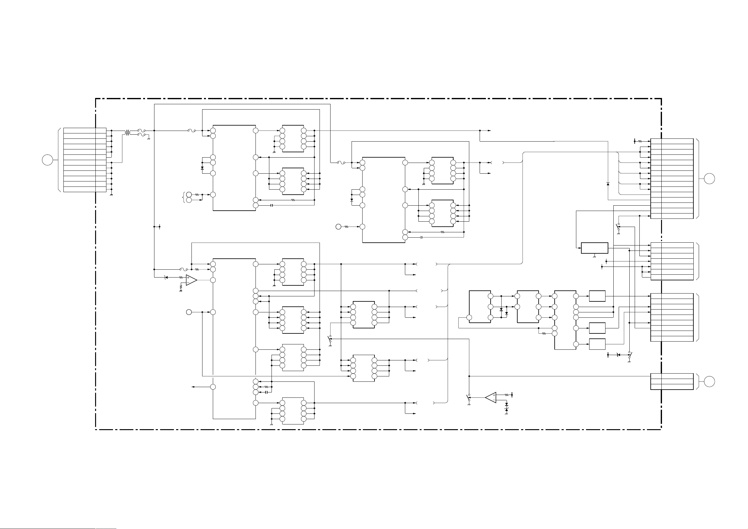
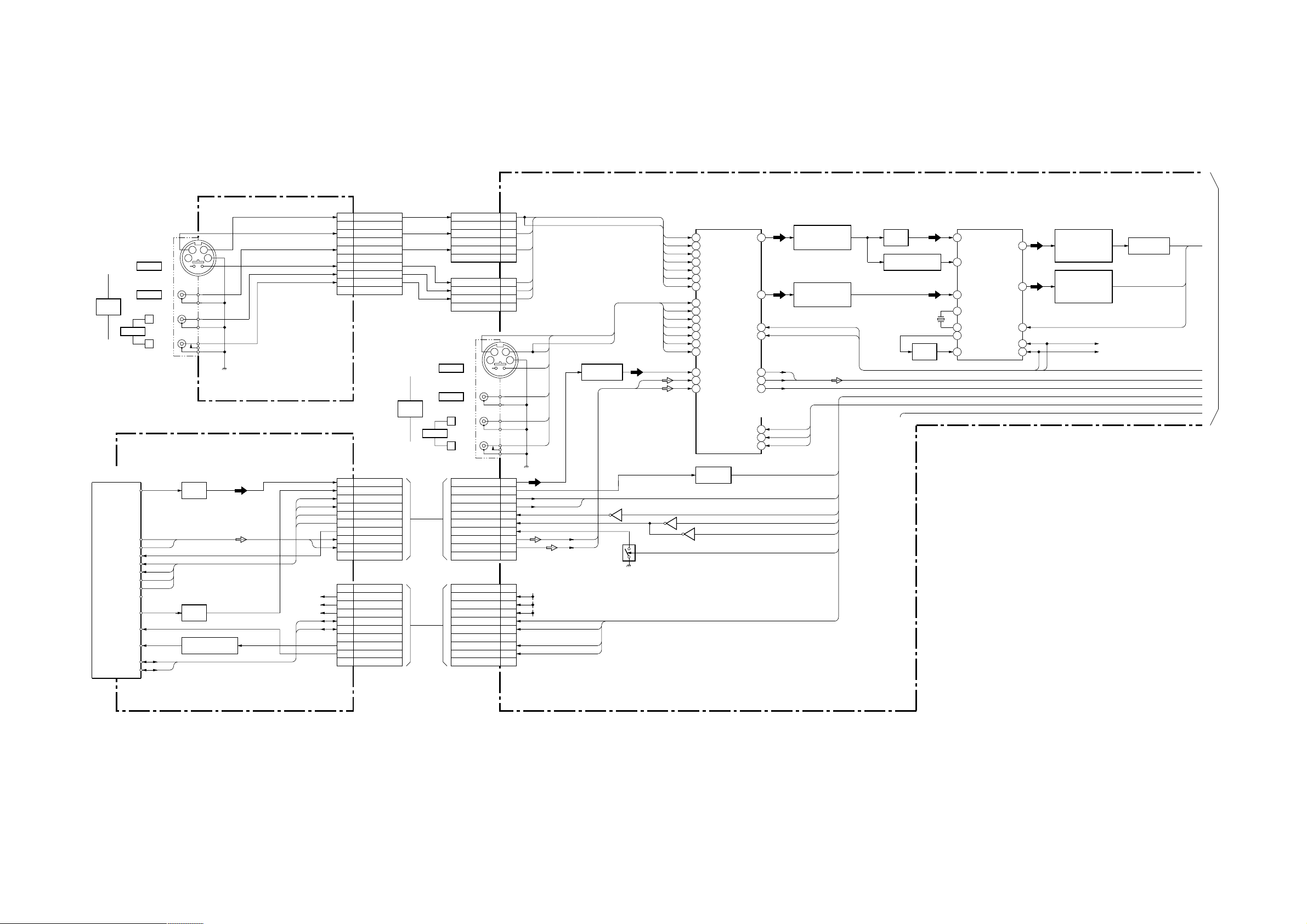
3-1. BLOCK DIAGRAMS
SECTION 3
DIAGRAMS
D
TO G BAORD
CN8803
CN8605
16.5V
16.5V
16.5V
16.5V
16.5V
16.5V
GND
GND
GND
GND
GND
GND
10
11
12
IC8401
1
2
3
4
5
6
7
8
9
L8610 F8601
F8602
16.5V
D8432
TO 2/2
F8403
VREF5V
F8401
D8401
2
5
7
6
IC8408(1/2)
CONVERTER
VCC_SENSE14
VREF5
13
14
COMP
LH
17
10 STBY1
IC8402
CONVERTER
VCC24
6 CTSV_STBY
9
STBY1
POWERGOOD
10 STBY24TO 2/2
22
VREF5
OUT_d
LL
OUT_u
INV
FB
OUT1_D
REGSV-IN
LL1
OUT1_u
OUT2_u
LL2
INV2
FB2
OUT2_D
1713 VCC
18
19
2
3
27
12
21
28
29
17
18
15
14
19
Q8402
SW
G
D1
4
S1
D2
1
S2
D3
2
S3 D4
3 8
Q8401
SW
4
D1
G
1 6
D2
S1
2
D3
S2
D4S3
3
Q8407
SW
D1
G
4
D2
S1
1 6
D3
S2
2
D4S3
3
Q8405
SW
G
D1
4
S1
D2
1
S2
D3
2
S3 D4
3 8
Q8411
SW
D1
G
4
D2
S1
1 6
D3
S2
2
D4S3
3
Q8409
SW
G
D1
4
S1
D2
1
S2
D3
2
S3 D4
3 8
5
6
7
IC8404
F8405
5
7
8
D8420
TO 2/2
5
7
8
5
6
7
5
7
8
5
6
7
3 STBY10
1
2 6
3
4
Q8406
1
2
3
4 8G
CONVERTER
VCC13
14 VCC_SENSE
13
VREF5
14
COMP
17
LH
Q8404
SW
D1
S1
D2
S2
D3
S3
D4
G8
Q8408
SW
S1
D1
S2
D2
S3D4D3
OUT_d
OUT_u
5
7
5
6
7
LL
INV
FB
17
18
19
2
3
Q8417
G
4
S1
1 6
S2
2
3
Q8418
G
4
S1
1
S2
2
S3 D4
3 8
STBY5V
STBY5V
3.3V ALERT
PANEL5V
PANEL5V
D5V
D5V
D3.3V
D3.3V
SW
SW
D1
D2
D3
D4S3
D1
D2
D3
5
7
8
5
6
7
2 9LOAD
AU12V
IC8601
OUTA
14
OUTB
13
IC8408(2/2)
1
Q8413
9V
9V
CN8602
DCIN ALERT
16.5V
D8406
Q8627
Q8621,8622
SW
D5V
16.5V
IC8602
DECODER
Y0
1A
2 5
3
VREF5V
2
D8431
D8434
7
Y2
B
Y3
3
7
9
11
2
4
IC8603
Q8623
1
6
8
10
13
14
INV
Q8625
INV
Q8624
INV
16.5V
D8606
Q8619
A(1/2)
1
D3.3V
3
D3.3V
4
D3.3V
5
9
10
PANEL5V
13
PANEL5V
14
STBY5V
17
STBY5V
18
3.3V ALERT
21
5V ALERT
22
DIMMER
23
BACK LIGHT
24
PANEL DET
25
CN8603
DIMMER
10
BACK LIGHT
9
PANEL DET
8
6
16.5V
3
16.5V
2
16.5V
1
CN8606
9
BRTP-C
8
7
BRTP-B
6
BRTP-A
5
4
BRT C
3
2
1
CN8402
1
B/L VCC
2
3
PANEL DET(NC)
D5V
D5V
D5V
G
NC
OLS
G
G
G
F
TO B2 BOARD
CN1003
TO PANEL UNIT
INVERTER
TO PANEL UNIT
INVERTER
C
TO G BOARD
CN8804
(POWER SUPPLY)
KLV-23HR1 (UC) 3-1
VIDEO 2
INPUT
AUDIO
S VIDEO
VIDEO
L
R
J9501
34
12
V
L
R
U1
CN9501
1
C2
2
G
3
Y2
4
G
5
V2
6
G
7
S-2
8
LV2
9
RV2
10
G
(INPUT TERMINAL)
VIDEO 1
INPUT
AUDIO
S VIDEO
VIDEO
L
R
CN9003
C2
G
Y2
G
V2
G
CN9004
S-2
LV2
RV2
G
J9003
A(2/2)-1
1
2
Y2
3
4
V2
5
6
S2
1
LV2
2
RV2
3
4
Y1
43
V
L
R
C1
21
S1
V1
LV1
RV1
S2-1
Q6020,6011
BUFFER
S2-1
VIDEO
AUDIO L
AUDIO R
C2
Y210
12
C2
9
LV2
11 RV2
1314S2-1
S2
V11
3Y1
52C1
LV1
RV14
S2-1
6
S1
7
47
TV
48 LTV
RTV46
IC3201
AV SW
YOUT1
COUT1
SDA
SCL
ROUT1
LOUT1
VOUT2
V3
LV3
RV3
IC2004
438V2
45
27
26
41
39
33
15
16
18
Q3209,2019,2018
Y
Q3207,2016,2012
C
FL2004
LPF
FL2003
LPF
SDA_B_5V
SCL_B_5V
AUDIO L/R
Q2014
BUFFER
Q2011,2013,2015
SYNC SEP.
X2001
20MHz
Q2002
OSC
Y
C
3D COMB FILTER
AYI88
CSI
76
96 ACI
XI47
48
XO
50 FSCO
52 FSCI
AYO
ACO
RSTB
SCL
SDA
Q2004,2005,2008
Y
Q2003,2006,2007
C
Q2010,2022
FL2002
L-P.F
Q2009,2023
FL2001
L-P.F
84
83
Q3210,-3212
BUFFER
YOUT
COUT
TO
A(2/2)-2
57
59
60
SDA_B_5V
SCL_B_5V
3DRST
TU6400
TUNER
DET OUT2
L OUT
R OUT
MUTE
FMONO
MODE
BIL LED
ST LED
DET OUT
RFAGC
AFT
SCL
SDA
TU
Q6402
BUFFER
Q6403
BUFFER
Q6401,6404,6405
VIDEO
AUDIO L/R
BUFFER
(TUNER)
9V
30V
5V
10
9
8
7
6
5
4
3
2
1
10
9
8
7
6
5
4
3
2
1
CN6401
CN6400
DETOUT2
DETOUT
STIND
BIIND
MODE
FMONO
MUTE
ROUT
LOUT
GND
GND
9V
30V
5V
SCL
SDA
AGC DET(NC)
RF AGC
AFT
GND
CN6007
DETOUT2
DETOUT
STIND
BIIND
MODE
FMONO
MUTE
ROUT
LOUT
GND
CN6006
GND
9V
30V
5V
SCL
SDA
AGC DET(NC)
RF AGC
AFT
GND
SYNC DET
STLED
BILED
FMONO1
FMONO2
MUTE
Q6062
INV
Q6025,6026
SYNC,SEP
Q6063
INV
VIDEO
10
9
8
7
6
5
4
AUDIO R
3
2
1
10
9
8
7
6
5
4
3
2
1
AUDIO L
9V
30V
5V
SCL TU
SDA TU
AGC
AFT
Q6060
INV
Q6011
MUTE
KLV-23HR1 (UC) 3-2
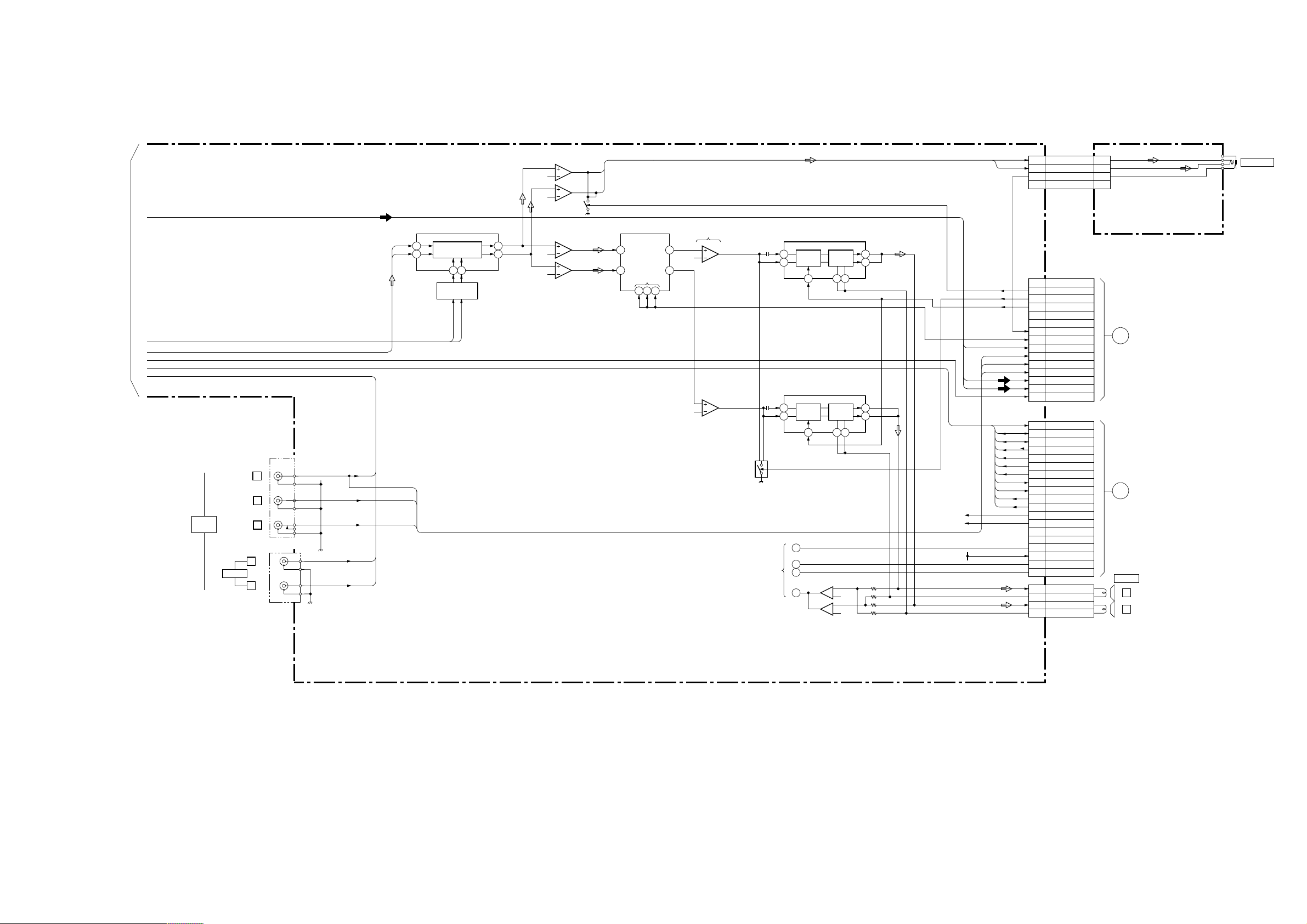
TO
A(2/2)-1
VIDEO 3
INPUT
AUDIO
PR
PB
Y
AUDIO R
AUDIO L
CN7001
C
Y
1
2
3
4
1
2
3
4
5
6
8
9
11
13
15
17
19
21
25
24
23
22
21
20
19
18
17
16
15
9
8
6
5
4
3
2
1
4
3
2
1
HP-R
HP-L
HP-DET
HP-GND 4
CN3201
LINE MUTE
HP MUTE
SP MUTE
SLEEP MUTE
TU-HS(NC)
TU-VS(NC)
HP DET
SRS CONT
DEVICE RST
Pr
Pb
Y
3D-C
3D-Y
V OUT23
CN3202
SYNC DET
SCL TU
SDA TU
MUTE
FMONO2
FMONO1
MODE
BILINGUAL
STEREO
AGC
AFT
SDA B 5V
SCL B 5V
SCL B(NC)
SDA B(NC)
POWER1
POWER2
POWER3
POWER4
CN7002
SP R+
SP R-
SP L+
SP L-
IC7013
HP AMP
5
7
6
3
1
2
AUDIO R
Y/C
L
11
R
AUDIO L/R
J9002
Y
PB
PR
L
R
V
L
R
J9004
V3
Y
PB
PR
L3
R3
IC7003
VOL/AP
BASS/TREBLE
VOL LOUD/ ATT
1920
Q7006,7007
LEVEL SHIFT
AUDIO L
IC7004
COMPARATOR
3
17
166
1
2
AUDIO L
5
7
6
AUDIO R
Q7001,7008,7009
MUTE
IC7002
AP
42
41
INL
INR
MODE
OUTL
OUTR
262322
IC7006
AMP
2
30
29
1
3
5
7
6
AUDIO L/R
IC7010
AUDIO AMP(L)
1
GAIN
ADJ
2 11
51415
IC7009
AUDIO AMP(R)
1
GAIN
ADJ
Q7011,7012,7016
4
TO 1/2
1
3
IC7011
2
COMP
7
1
GATE
DRIVE
GATE
DRIVE
15145
5
6
3
2
10
AUDIO L
10
112
AUDIO R
SDA B 5V
SCL B 5V
PANEL 5V
CN7601
1
AUDIO R
2
3
H2
AUDIO L
(HEADPHONE)
H
TO B2 BOARD
CN3001
G
TO B2 BOARD
CN1007
SPEAKER
R
L
J7601
HEADPHONE
A(2/2)-2
(AV SW,3D COMB FILTER,SUB CPU,AUDIO AMP)
KLV-23HR1 (UC) 3-3

H
TO A(2/2)BOARD
CN3201
G
TO A(2/2)BOARD
CN3202
F
TO A(1/2)BOARD
CN8602
B
TO H1 BOARD
CN1501
A
TO H3 BOARD
CN1602
CN3001
V OUT
3D-Y
3D-C
Y
Pb
Pr
SRS CONT
HP DET
SLEEP MITE
SP MUTE
HP MUTE
LINE MUTE
CN1007
SDA B 5V
SCL B 5V
SDA B
SCL B
POWER 4
POWER 3
POWER 2
POWER 1
AGC
STEREO
BILINGUAL
MODE
FMONO1
FMONO2
MUTE
SYNC DET
CN1003
PANEL DET
BACK LIGHT
DIMMER
5V ALERT
3.3V ALERT
PANEL 5V
PANEL 5V
DC IN ALERT
CN1002
TXD
RXD
RES
MD0
MD1
MD2
P-TXD
P-RXD
SCK
P-RES
B INT
RXD
TXD
CN1006
SCL A
SDA A
B INT
CN1004
KEY 1
KEY 2(NC)
POWER INT
P SAVE LED
STBY LED
POWER LED
SIRCS
3
5
7
9
11
13
15DEVICE RET
17
18
22
23
24
25
18
17
21
20
25
24
23
22
10
11AFT
9
8
7
6
5
4
1
25
24
23
22
21
14
13
1
2
3
4
6
7
8
9
10
11
12
15
16
17
4
3
2
1
2
3
7
8
9
10
Q3501
BUFF
X3501
14.318MHz
3D-Y
3D-L
Y
Pb
Pr
SCL B 5V
SDA B 5V
Q1009
Q1010
LEVEL
SHIFT
Q1001
(NC)
STBY 3.3V
Q1013,1014
14
6 AD IN
IO
11
X0
25
26
X1
STBY3.3V
LEVEL
SHIFT
IC1010
AUTO WIDE
IC1007
IC3601
Q3601,3602 BUFF
IC3501
16SDA
15
SCL
Y/C Y
Y
Pb
Pr
SDA B
SCL B
TEMPERATURE
1 SDA
2
HP DET
DEVICE RST
FMONO2
HP MUTE
SP MUTE
SLEEP MUTE
LINE MUTE
BILINGUAL
SRS CONT
Q1015
RESET
GEN
Q1016
D1002
Q1006
IC1008
EEPROM
SCL
SDA
WC
V-CHIP/CCD
53 59
IC3603
COMPONENT-TEXT
1
YIN1
2
PbIN1
PrIN1
3
YO
PbO
PrO
IC1011
SENSOR
SCL
120
121
74
73
8
7
6
5
128
AGC
126
15
MODE
16
22 PB7
23
24
2926PA5
AFT
STEREO
12
13
63
FMONO 1
17
119
125
123
124
115
117
141
139
92
143
144
1
55
54
14
IC1009
24
39
32
1
6
5
7
79
77
78
88
113
114
60
36
37
35
48
62
63
73
74
68
69
3D-Y
3D-C
R
9
R
G
10
G
B
B
11
YS
YS
20
YM
YM
21
D-Y
16
D-PB
17
D-PR
18
IC1006
MICROCOMPUTER
P47
P90
PD1
PD0
PC3
PC2
PC1
PC0
P97
P95
PB1
PB2
PA0
PA1
PA2
P96127
RXD3
SCK3
PE0
PB3
P46
PA428
P94
P92
P93
P42
P44
TXD1
RXD1
RES
MD0
MD1
MD2
RXD4
TXD4
PB0
WDTOVFN
EMLE
PD6
PD4
PD5
PF4
P40
P41
P84
PH1
PH2
PH0
P16
OSD R
OSD G
OSD B
OSD YS
OSD YM
OSD VS
OSD HS
FL3402,Q3403,3404,3407,3408
FL3401,Q3401,3402,3405,3406
P26
57
P25 56
PF3
87
PF2
86
85
PF1
84
PF0
46
P14
42
P10
PE5 68
P63
104
105
P64
81
P60
PC5 11
27PA3
P65
106
97XTAL
96EXTAL
LPF
LPF
R
G
B
BUFF
D-Y
D-PB
D-PR
A
HSDEC
VSDEC
EXT V
EXT H
POL V
POL H
H COUNT1
V COUNT1
PANEL 5V
CLKEN
PW-BSY1
PW-BSY2
PANEL V
POWER 6
PIC MUTE
PW RST DET
P-TXD
P-RXD
PW RST
X1001
16.384MHz
C
B
A
Q3309
Q3307,3606
BUFF
Q3306,3605
BUFF
Q3308,3607
BUFF
X3001
20.25MHz
CLKDEC
HSDEC
VSDEC
SDA B
SCL B
DEV RST
B
V COMP
VSDEC
IC5508
BUFFER
12
16
14
18
9
713
IC3001
VIDEO DECODER
VN172
71 CN1
YN4
3 R1 IN
2
G1 IN
1
B1 IN
YN3
74
5
Y2 IN
4
CB2 IN
6
CR2 IN
6263XTAL1
XTAL2
HS
56
57
VS
28
LLC1
SDA
SCL1413
15
RESQ
IC3608
VS-SW
1 5
ACOM
6
I
B
7
8
15
4
17
6
16
2
18
11
13
11
3.3V
Y
0-7
C
0-7
FB1 IN
P52
YS SW
IC5503
SYNC SEP
EXIV
EXIH
POLV
POLH
HDRV
VDRV
31-34,
37-40
41-44,
47-50
79
135
1 4
VIDEO
ACTIVE
FILTER
IC3604
SW
SW OUT
IN1
Y
Pb
Pr
3
Q3002
8
8
R-Y/B-Y
2
D3.3V
D5V
Y DT0-7
UV DT0-7
CLKDEC
SDA B
SCL B
DEV RST
C
LPF
LPF
LPF
D3.3V
HSDEC
VSDEC
IC5507
+3.3V
REG
IC5506
+3.3V
REG
FL5504
FL5502
FL5503
199-206
189-196
3 W13ID
4
IHDD
5
IVDD
RXI
9089XOC
XRST67
54
RAIN
43
BAIN
48
GAIN
SOG IN49
IC3302
DRC-MF
DIYD
0-7
DICD
0-7
ADDR0-11
DYO2-9
DRO2-9
DBO2-9
XV9O
XH9O
CS4I
RPLHD
HREF
CS4O
DQ0-15
XCAS
XRAS
IC5505
AD CONV
RED 0-7
GREEN 0-7
BLUE 0-7
122-129
133-140
147-154
99
98
97
96
95
117
13-20,
25-32
35-42,
46-49
10
DOM
XWE
9
7
8
XCS
DATACK
HSOUT
CLAMP
COAST
IC3301
+1.8V
REG
8
8
8
DQ0-15
8
12
70-77
2-9
12-19
SDA
SCL
XDRCVS
XDRCHS
4
5
A0-11
67
66
64VSOUT
38
29
65SOGOUT
57
56
Y0-7
V0-7
U0-7
IC3304
PLL WRITE
FREQ
DET
IC3303 DRAM
35
CLK
2,3,5
6,8,9
11
,12,
39
40,42,43
,46,
48
45
49
19-24,
27-32
36
UBOM
14
LBOM
15
WE
16
CAS
17
RAS
1811
CS
ADR 0-7
8
ADG 0-7
8
ADB 0-7
8
ADCLK
HSOUT
VSOUT
CLAMP(BLKSPL)
COAST
SOGOUT
ADSDA
ADSCL
D5V
DRC Y/U/V
Q3305
D5V
VCC
DROP
DQ0-15
ADDR0-11
Q3304
Y/R-Y/B-Y
VCO12 36 LPF
54CLK
B2
Y0-7
ADR0-7
V0-7
ADG0-7
U0-7
ADB0-7
XDRCVS
XDRCHS
54CLK
CLKEN
ADCLK
HSOUT
VSOUT
CLAMP(BLKSPL)
COAST
SOGOUT
IC5013
PW-BSY1
PW-BSY2
PANEL V
POWER 6
PANEL 5V
IC5011
AWITCH
9 8
2 3
1,10,13
IC5014
2
1 RST
89,10
8
8
8
8
8
8
R-Y
8
8
8
B-Y
X5001
14.31818MHz
1112
IC5014
12
LATCH
11
ADSDA
ADSCL
PIC MUTE
P-TXD
P-RXD
PW RST DET
PW RST
Y
953
155,
158-164
147-154
131,132
139-141,
144-146
137
XOXI138
120
GVS
126
VVS
119
GFBK
127
VHS
118
GCLK
125
VCLK
PORTA68
GCOAST
124
GHSSOG
123
129
VFIELD
PORTA4
10
9
PARTA5
PORTA014
PORTA1
13
7
POTRA7
TXD
45
46
RXD
IC5003
SCAN CONVERTER
VGR0-7
VGG0-7
VGB0-7
DR0-7
DG0-7
DB0-7
D0-15
A1-19
PORTA2
72-76,
81-83
62-67,
70,71
54-61
DEN
DHS
DVS
DCLK
165-174
177-180,
185,186
187-199,
202-207
ROMWE
ROMOE
NMI
CS0
CS1
TRSTN4447
RESET
1
1
86
85
84
88
4
3
208
5
6
12
8
8
8
PANEL V
POWER6
IC5009
RESET
VOLTAGE
DET
IC5006
RESET
VOLTAGE
DET
50-52,
54-56
10-12,
15,16
18-20,
22-24
PANEL 5V
16 16
19 19
6
IC5013
11
2
2
2,3
4,
6-8,
14
TC6
30
TC4
27
TC5
28
CLK IN
31
PDWN
32
IC5013
P1.8V
P3.3V
IC5004
LVDS TX
TD0,1
TA0-5
TD2,3
TA6,
TB0-4
TD4,5,
TB5-6,
TC0-3
PROM(FLASH MEMORY)
16
29-36,
38-45
1-8,
19
16-25,
48
11
WE
28
OE
26
CE
RESET
12
IC5013
5
3
4
12
13
IC5007
+1.8V
REG
IC5008
+3.3V
REG
TA-
TA+
TB-
TB+
TC-
TC+
TCLK-
TCLK+
TD-
TD+
IC5002
DQ0-15
A0-18
2
1
D3.3V
D5V
48
47
46
45
42
41
40
39
38
37
12,13
18
17
15
14
12
11
9
8
6
5
2
1
A25-A32
B25-B32
A5-A12
B1-B11
B17
B15
B21
B18
B19
B23
B22
B26
CN5001
TX0-
TX0+
TX1-
TX1+
TX2-
TX2+
TCLK-
TCLK+
TX3-
TX3+
CN5002
D0-15
A1-19
ROMWEN
ROMOEN
BOOTWE
FCEN
ROMWEN
VCC
VCC
NMI
CS2
CS3
TO LCD
PANEL
TO LCD
PANEL
(CPU,VIDEO DECODER,DRC-MF,AD CONVERTER)
KLV-23HR1 (UC) 3-4

(KEY)
12
11
10
9
8
7
6
5
4
3
2
1
GND
GND
GND
GND
GND
GND
16.5V
16.5V
16.5V
16.5V
16.5V
16.5V
CN8803
CN8801
DC IN
14.5V
9A
3
5
7
1
2
6
8 4
D
D
D
DS
S
S
S
Q8801
SW
SW
Q8802
D
D
D
D
4
8
62
1
7
5
3
19
13
14
18
20
17
OUT_U
LL
VREF5
IC8801
COMP
12
8
STBY
10
F8802,8801
F8803
FL8001
VCC
VCC-SENSE
OUT_d
D8801
10
9
8
7
6
5
4
3
2
1 GND
GND
GND
GND
GND
12V
12V
12V
12V
12V
10P
CN8802
TO
INVERTER
3
2
1
PANEL DET(NC)
GND
B/L VCC
3P
CN8804
L8801
D
TO A(1/2)BOARD
C
TO A(1/2)BOARD
(POWER SUPPLY)
G
F8807
CN8605
BOARD
CN8401
F8806
H1
S1501-1504
KEY
S1508
POWER
CN1501
1
KEY1
2
KEY2(NC)
3
POWER INT
4 GND
B
TO B2 BOARD
CN1004
H3
Q1601
D1604
POWER
Q1602
VCC OUT
IC1601
SIRCS
1
2
3
4
5
6
D1605
STBY
Q1603
(SIRCS,LED)
CN1602
GND
STBY5V
P SAVE LED
STBY LED
POWER LED
SIRCS
A
TO B2 BOARD
CN1004
KLV-23HR1 (UC) 3-5
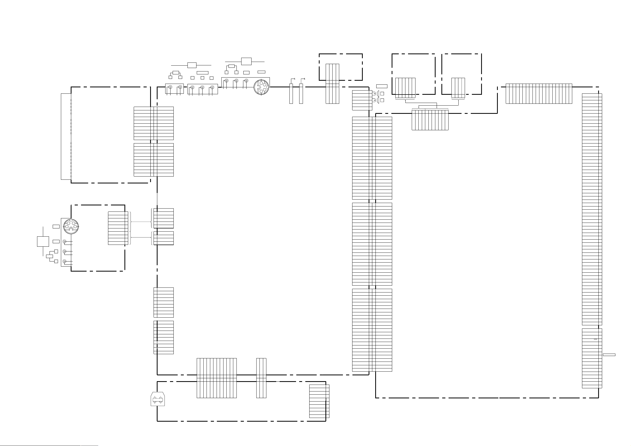
3-2. FRAME DIAGRAM
30V
5V
SCL
SDA
AS
RF AGC
VIF
9V
AFT OUT
GND
TU6400
DET OUT2
DET OUT
ST IND
BIL IND
MODE
F MONO
NC
MUTE
M OUT
R OUT
L OUT
S
VIDEO
INPUT
34
12
VIDEO
S1
2
AUDIO
VIDEO
V
J9501
L
L
R
R
U1
CN9501
10P
WHT
TU
C2
GND
Y2
GND
V2
GND
S-2
LV2
RV2
GND
CN6400
10P
WHT
CN6401
10P
WHT
1
2
3
4
5
6
7
8
9
10
GND
30V
SCL
SDA
GND
RF AGC
AFT
GND
DET OUT2
DET OUT
ST IND
SAP IND
MODE
FMONO
MUTE
R OUT
L OUT
GND
TO INVERTER
TO INVERTER
DC IN
14.5V
9V
5V
10
1
9
2
8
3
7
4
6
5
5
6
4
7
3
8
2
9
1
10
10
1
9
2
8
3
7
4
6
5
5
6
4
7
3
8
2
9
1
10
1
2
3
4
5
6
1
2
3
4
1
2
3
4
5
6
7
8
9
1
2
3
4
5
6
7
8
9
10 DIMMER
GND
9V
30V
5V
SCL
SDA
AGC DET
RF AGC
AFT
GND
OUT2
DET OUT
ST
BIL
MODE
FMONO
MUTE
R
L
GND
C2
GND
Y2
GND
V2
GND
S-2
LV2
RV2
GND
GND
GND
OLS
BRT C
NC
BRTP-A
BRTP-B
GND
BRTP-C
16.5V
16.5V
16.5V
GND
GND
D5V
GND
PANEL DET
BACK LIGHT
AUDIO
RL
LR
J9004
CN6006
10P
CN6007
10P
CN9003
6P
CN9004
4P
CN8606
9P
CN8603
10P
CN8801
VIDEO 3
INPUT
COMPONENT
PR PB
J9002
16.5V
123456789
123456789
16.5V
16.5V
16.5V
16.5V
16.5V
16.5V
16.5V
Y
16.5V
16.5V
CN8605
12P
16.5V
GND
GND
16.5V
CN8803
12P
WHT
CN7601
VIDEO
2
INPUT
AUDIO
VIDEO
VIDEO
S1
S
1
V
3
4
2
1
GND
CN9001
1P
1
GND
CN9002
1P
L
R
L
R
J9003
A
CN8402
4P
B/L VCC
GND
GND
GND
GND
GND
GND
101112
101112
GND
GND
GND
GND
GND
G
123
123
GND
B/L VCC
CN8804
3P
WHT
PANEL DET
12V
10P
WHT
12V
12V
12V
GND
GND
PANEL DET
CN8802
4P
STBY LED
POWER LED
10
SIRCS
11
NC
CN1501
4P
WHT
KEY1
KEY2
123
POWER INT
4 GND
B2
TO
LCD PANEL
1011121314151617181920
TX0-
TX0+
GND
GND
GND
TX1+
GND
CN5001
20P
BRN
TX2+
TX2-
TX1-
TX3-
GND
GND
TCLK-
TCLK+
TX3+
123456789
VCC
VCC
GND
GND
CN5002
70P
(N.C.)
CN1002
18P
GND
GND
GND
GND
A10
GND
BHENN
GND
ROMOEN
GND
ROMOEN
3.3V
ROMWEN
3.3V
ROMWEN
3.3V
CS2
3.3V
CS3
GND
RESETN
GND
NM1
GND
FCEN
GND
BOOTWE
GND
VPPEN
GND
TXD
RXD
RES
MD0
MD1
MD2
P-TXD
P-RXD
SCK
P-RES
B_INT
RXD
TXD
GND
A19
A18
A17
A16
A15
A14
A13
A12
A11
A9
A8
A7
A6
A5
A4
A3
A2
A1
A0
D15
D14
D13
D12
D11
D10
D9
D8
D7
D6
D5
D4
D3
D2
D1
D0
NC
NC
6V
6V
6V
6V
VIN
VIN
A1
B1
A2
B2
A3
B3
A4
B4
A5
B5
A6
B6
A7
B7
A8
B8
A9
B9
A10
B10
A11
B11
A12
B12
A13
B13
A14
B14
A15
B15
A16
B16
A17
B17
A18
B18
A19
B19
A20
B20
A21
B21
A22
B22
A23
B23
A24
B24
A25
B25
A26
B26
A27
B27
A28
B28
A29
B29
A30
B30
A31
B31
A32
B32
A33
B33
A34
B34
A35
B35
1
2
3
4
5
6
7
8
CPU&PWROM
9
10
11
12
13
14
15
16
17
18
H2 H1H3
HP DET
HP-L
HP-R
GND
123
4
123
4
GND
HP-L
HP-R
HP-DET
CN7002
CN7001
4P
CN8602
CN3202
CN3201
1
2
12V
3
12V
4
5
TO INVERTER
6
7
GND
8
GND
9
10
6P
WHT
25P
25P
25P
SP L SP L +
SP R SP R +
NC
NC
PANEL DET
BACK LIGHT
DIMMER
5V ALERT
3.3V ALERT
GND
GND
STBY 5V
STBY 5V
GND
GND
PANEL 5V
PANEL 5V
GND
GND
D 5V
D 5V
GND
GND
GND
D 3.3V
D 3.3V
D 3.3V
GND
DCIN ALERT
SYNC DET
SCL TU
SDA TU
MUTE
FMONO2
FMONO1
MODE
BILINGUAL
STEREO
AGC
AFT
GND
GND
9V
9V
GND
SCL B 5V
SDA B 5V
GND
SCL B
SDA B
POWER1
POWER2
POWER3
POWER4
LINE MUTE
HP MUTE
SP MUTE
SLEEP MUTE
TU HP
TU VP
GND
HP DET
SRS CONT
GND
DEVICE RST
GND
Pr
GND
Pb
GND
Y
GND
3D-C
GND
3D-Y
GND
V OUT
GND
GND
SPEAKER
1
L
2
3
R
4
5
6
25
25
PANEL DET
24
BACK LIGHT
24
23
DIMMER
23
22
5V ALERT
22
21
3.3V ALERT
21
20
GND
20
19
GND
19
18
STBY 5V
18
17
STBY 5V
17
16
GND
16
GND
15
15
14
PANEL 5V
14
13
PANEL 5V
13
12
GND
12
11
GND
11
10
D 5V
10
9
9
D 5V
8
GND
8
7
GND
7
6
GND
6
5
D 3.3V
5
4
D 3.3V
4
3
D 3.3V
3
2
GND
2
1
1
DCIN ALERT
SYNC DET
1
1
2
SCL TU
2
3
SDA TU
3
4
MUTE
4
FMONO2
5
5
6
FMONO1
6
MODE
7
7
BILINGUAL
8
8
STEREO
9
9
AGC
10
10
AFT
11
11
GND
12
12
13
GND
13
14
9V
14
9V
15
15
16
GND
16
17
SCL B 5V
17
18
18
SDA B 5V
19
GND
19
20
20
SCL B
21
21
SDA B
22
POWER1
22
23
POWER2
23
24
POWER3
24
25
POWER4
25
LINE MUTE
25
1
24
HP MUTE
2
23
SP MUTE
3
22
SLEEP MUTE
4
TU HP
21
5
TU VP
20
6
GND
19
7
18
HP DET
8
SRS CONT
17
9
GND
16
10
DEVICE RST
15
11
GND
14
12
Pr
13
13
GND
12
14
11
Pb
15
10
GND
16
9
Y
17
8
GND
18
7
3D-C
19
6
GND
20
3D-Y
5
21
4
GND
22
3
V OUT
23
2
GND
24
1
GND
25
GND
1
CN1003
25P
CN1007
25P
CN3001
25P
CN1602
6P
P SAVE LED
STBY5V
STBY LED
POWER LED
SIRCS
65432
123456789
GND
GND
KEY2
KEY1
POWER INT
CN1004
11P
STBY 5V
P SAVE LED
KLV-23HR1 (UC) 3-6
3-3. CIRCUIT BOARDS LOCATION 3-4. SCHEMATIC DIAGRAMS AND PRINTED WIRING BOARDS
Note:
• All capacitors are in µF unless otherwise noted. (pF: µµF)
Capacitors without voltage indication are all 50 V.
• Indication of resistance, which does not have one for rating electrical power, is as follows.
Pitch: 5 mm
Rating electrical power 1/4 W (CHIP : 1/10 W)
• All resistors are in ohms.
• : nonflammable resistor.
• : fusible resistor.
• : internal component.
• : panel designation, and adjustment for repair.
• All variable and adjustable resistors have characteristic curve B, unless otherwise noted.
• : earth-ground.
• : earth-chassis.
• When replacing the part in below table, be sure to perform the related adjustment.
• All voltages are in V.
• Readings are taken with a 10 M digital multimeter.
• Readings are taken with a color-bar signal input.
• Voltage variations may be noted due to normal production tolerances.
•
• Circled numbers are waveform references.
: Can not be measured.
*
• : B + bus.
• : B – bus.
Note: The components identified by shading and
mark ! are critical for safety. Replace only
with part number specified.
Note: Les composants identifiés par un tramé et
une marque ! sont critiques pour la
sécurité. Ne les remplacer que par une pièce
portant le numéro spécifié.
• Divided circuit diagram
Schematic diagrams of A and B2 boards are divided into serveral pieces.
Information to where the line is to be connected is printed at the end of
wach line.
For example, [ TO A1/5, A2/5 ] means the line is connected to
Ref. No. 1 of A (1/5) and A (2/5) schematic diagrams.
TO A1/5, A2/5
Circuit diagram division code
H1 board
H3 board
B2 board
TU board
A board
G board
H2 board
U1 board
Terminal name of semiconductors in silk screen
printed circuit ( )
Device Printed symbol Terminal name
Transistor
1
Transistor
2
3
Diode
4
Diode
Diode
5
Diode
6
Diode
7
8
Diode
Diode
9
Diode
0
Diode
!¡
Diode
!™
Transistor
!£
(FET)
Transistor
!¢
(FET)
Transistor
!∞
(FET)
Transistor
!§
Transistor
!¶
Transistor
!•
Transistor
!ª
Transistor
@º
Transistor
@¡
Transistor
@™
Transistor
@£
Discrete semiconductot
–
(Chip semiconductors that are not actually used are included.)
*
Collector
Base
Collector
Base
Cathode
Cathode
Anode
Cathode
Anode
Common
Anode
Common
Anode Cathode
Common
Anode
Common
Anode Anode
Common
Cathode
Common
Cathode
Anode
Anode
Cathode
Drain
Drain
B1 E1
C2
B2 C1
E2
B2 E2
C1
B1 C2
E1
B2 E2
C1
B1 C2
E1
B2 E2
C1
B1 C2
E1
E2
B1 E1
C2
(B2)
E1
B1
C1
(B2)
E1
E2
C2
Emitter
Emitter
Anode
(NC)
(NC)
Cathode
Anode
Cathode
Cathode
Cathode
Anode
Anode
Source
Gate
Source
Gate
Source
Drain
Gate
Emitter
Collector
Base
C1(B2)
E2
C2
B1
C1
Circuit
D
G
D
S
B1
B1
B1
B1
B1
B1
D
G
S
S
D
G
C1
E1
C1
E1
E1
C1
E2
C1
C1
G
S
C2
B2
E2
C2
B2
E2
E2
B2
C2
C2C1(B2)
E2
E2E1(B2)
C2
C2E1(B2)
C2
Ver.1.6
KLV-23HR1 (UC) 3-7
(1) A Board
0
1
VIDEO
AUDIO L
AUDIO R
VIDEO
VIDEO
VIDEO
VIDEO
VIDEO
0
0
0
0
0
0
0
TU5V
D5V
9V
30V
9V
TO(2/5)
TO(2/5)
(NC)
(NC)
(VIDEO AMP)
B-SS11640<UC.>-A..-P1
SYNC SEP
SYNC SEP
TO(2/5)
BUFF
INV
INV
INV
INV
TO(2/5)
DC-DC CONV.
TO TU BOARD
CN6401CN6400
TO TU BOARD
VPHS-SEP
A(1/5)
PIAKING
GND
GND
MUTE
AGC DET
GND
LOUT
ROUT
FMONO
MODE
BILED
STLED
DET OUT
DET OUT2
AFT
RFAGC
SDA
SCL
5V
30V
9V
VD
GND
T1
DK
OSC
VIN
1
2
3
4
5
6
7
8
9
10
123
4 5 6
1
2
3
4
5
6
7
8
9
10
CN6007
IC6001
C6012
C6014
JL6031
JL6032
C6010
C6011
C6007
C6016
C6008
JL6048
JL6049
JL6050
JL6051
JL6052
JL6053
JL6054
JL6055
JL6056
JL6057
JL6058
JL6059
JL6060
JL6061
JL6062
JL6063
C6015
CN6006
L6006
C6085
C6022
L6020
L6021
Q6022
Q6021
C6086
C6088
L6002
L6003
L6004
L6005
L6022
D6005
R6054
JL6064
C6002
C6003
C6020
C6021
C6023
C6024
C6087
C6089
C6090
C6091
C6092
C6093
C6121
Q6060
Q6061
Q6062
Q6063
R6005
R6008
R6020
R6021
R6022
R6023
R6024
R6025
R6026
R6027
R6028
R6029
R6030
R6031
R6047
R6050
R6051
R6052
R6053
R6055
R6056
R6057
R6058
R6059
R6060
R6061
R6089
R6090
R6091
R6092
R6093
R6094
R6095
R6096
R6116
R6117
R6118
R6119
R6122
Q6011
Q6020
Q6025
Q6026
L6001
C6070
C6071
C6072
C6073
C6074
C6075
C6076
R6121
Q6070
Q6071
Q6072
Q6073
R6070
R6071
R6072
R6073
R6074
R6075 R6076
R6077
R6078
R6079
R6080
R6081
R6082
10P
TK11819MTL
10
16V
:AL-CP
47
16V
:AL-CP
100
10V
:AL-CP
47
16V
:AL-CP
2.2
:AL-CP
47
16V
:AL-CP
4.7
:AL-CP
2.2 :AL-CP
10P
100µH
:CHIP
47
16V
:AL-CP
#
#
#
#
#
47
16V
:AL-CP
4.7
35V
:AL-CP
22µH
:FR-CP
22µH
:FR-CP
22µH
:FR-CP
22µH
:FR-CP
1mH
MA111
#
0.1
25V
F:CHIP
0.022
F:CHIP
#
#
#
#
0.1
16V
B:CHIP
0.22
16V
B:CHIP
0.001
B:CHIP
0.0047
B:CHIP
0.022
25V
B:CHIP
0.1
16V
B:CHIP
0.1
16V
B:CHIP
DTC114EUA
DTC114EUA
DTC114EUA
DTC114EUA
1k
:RN-CP
47
:CHIP
220
:CHIP
#
470
:RN-CP
#
750
:RN-CP
#
#
#
#
#
#
#
47
:CHIP
0 :CHIP
0 :CHIP
0 :CHIP
0 :CHIP
0 :CHIP
0 :CHIP
47k
:CHIP
47k
:CHIP
3.3k
:CHIP
10k
:CHIP
1k
:CHIP
1.5k
:CHIP
1M
:CHIP
3.9k
:CHIP
2.7k
:CHIP
4.7k
:CHIP
1M
:CHIP
4.7k
:CHIP
#
100
:CHIP
#
1k
:CHIP
#
0
:CHIP
2PD601AR-115
2PB709AR-115
2PD601AR-115
2PB709AR-115
1.2mH
#
#
#
#
#
#
#
0 :CHIP
#
#
#
#
#
#
#
#
#
##
#
#
#
#
#
#
TUNER VID
TUNER L
TUNER R
9V
TU5V
TU CTL
D3.3V
D5V
TU 9V
TU
5V
TU 9V
TU5V
TU
9V
SYNC_DET
TU HS
TU VP
TU5V
RF_AGC
SCL_TU
SDA_TU
AFT
STLED
BILED
MODE
MUTE
FMONO1
FMONO2
C
D
G
H
A
B
E
F
I
J
1
2
• A(1/5)BOARD WAVEFORM
1
1.1Vp-p ( H )
43
98765
10
11
12
13
14
15
KLV-23HR1 (UC) 3-8
 Loading...