

SONY KE-P37XS1, KE-P42XS1, KDE-P37XS1, KDE-P42XS1, KE-MX42A1 Service Manual
...
MODIFICATION HISTORY
MODEL NAME : KE-P37XS1/P42XS1
SERVICE MANUAL
PARTS No. : 9-878-248-02
* Blue characters are linking.
No. DATA CONTENTS
KE-MX42A1/MX42S1/MX42M1
KDE-P37XS1/P42XS1
1
2004. 6 Addition of Hong Kong, ME, China, OCE and UK Models.
Correction of The Parts Information. (P.83)

KE-P37XS1/P42XS1
KDE-P37XS1/P42XS1
KE-MX42A1/MX42S1/MX42M1
PANEL MODULE SERVICE MANUAL
PDP Module Name
FPF37C128128UB
FPF42C128128UC
KE-P37XS1 AEP Model
KE-P42XS1 AEP Model
KDE-P37XS1 UK Model
KDE-P42XS1 UK Model
KE-MX42A1 Hong Kong Model
KE-MX42A1 ME Model
KE-MX42M1 China Model
KE-MX42S1 OCE Model
FLAT PANEL COLOR TV

CONTENTS
1 OUTLINE
1.1 Panel Dimension ................................................................................................................1
1.2 Feature...............................................................................................................................1
1.3 Specification ....................................................................................................................... 2
1.3.1 Functional specification ...............................................................................................2
1.3.2 Display quality specification......................................................................................... 3
1.3.3 I/O Interface Specification............................................................................................ 4
1.3.4 Connector Specifications ............................................................................................. 7
2 SAFETY HANDLING of THE PLASMA DISPLAY
2.1 Notes to Follow During Servicing ..................................................................................... 10
3 NAME and FUNCTION
3.1 Configuration .................................................................................................................... 11
3.2 Block Diagrams ................................................................................................................12
3.2.1 Signal Diagrams ........................................................................................................12
3.2.2 Power Diagrams ........................................................................................................ 13
3.3 Function............................................................................................................................14
3.3.1 Logic board Function .................................................................................................14
3.3.2 Function of X-SUS Board ..........................................................................................23
3.3.3 Function of Y-SUS Board ..........................................................................................23
3.4 Protection function............................................................................................................24
4 PROBLEM ANALYSIS
4.1 Outline of Repair Flow......................................................................................................25
4.2 Outline of PDP Module Repair Flow................................................................................. 26
4.3 Checking the Product Requested for Repair....................................................................29
4.4 Operation Test Procedure ................................................................................................31
4.5 Fault Symptom .................................................................................................................32
4.6 Problem Analysis Procedure............................................................................................ 35
4.6.1 "The entire screen does not light.(Main power is turned off)” Problem analysis
procedure............................................................................................................................35
4.6.2 "Vertical line/Vertical bar" Problem analysis procedure..............................................42
4.6.3 "Horizontal bar" Problem analysis procedure ............................................................46
4.7 Problem Analysis Using a Personal Computer................................................................. 47
4.7.1 Connecting a computer..............................................................................................47
4.7.2 Preparing a computer ................................................................................................47
4.7.3 Problem Analysis Procedure......................................................................................48
5 Disassembling and Reassembling
5.1 Exploded View..................................................................................................................52

5.2 X-SUS Circuit Board Removal/Installation Procedure......................................................53
5.3 Y-SUS Circuit Board Removal/Installation Procedure......................................................55
5.4 ABUS-L Circuit Board Removal/Installation Procedure....................................................57
5.5 ABUS-R Circuit Board Removal/Installation Procedure ................................................... 59
5.6 LOGIC Board Removal/Installation Procedure................................................................. 61
5.7 Complete Panel Chassis Removal/Installation Procedure ............................................... 63
6 Operation Check and Adjustment Method
6.1 List of Check and Adjustment Items.................................................................................66
6.2 Check and Adjustment Method ........................................................................................ 67
6.2.1 Check and adjustment procedure..............................................................................67
6.2.2 Parameter adjustment ...............................................................................................68
6.2.3 Operation performance check items..........................................................................70
6.2.4 Heat Run Test............................................................................................................72
6.2.5 Logic board parameter forwarding.............................................................................74
6.2.6 Accumulation time reset ............................................................................................76
6.2.7 Setup before shipment...............................................................................................77
7 37A1 Mechanical drawing
FPF37C128128UB-63, 73 ................................................................................................78
8 THE PARTS INFORMATION ..................................................................................................83

Scope; 42A1 series
Caution
(Model name; FPF42C128128UC)
Before doing the service operation please be sure to read this service
analysis manual. This module has a lot of devices to secure the safety
against the fire, electric shock, injury and harmful radiation.
To maintain the safety control, please follow the instructions and remarks
described in this service analysis manual.

1 OUTLINE
The module is a plasma display module which can be designed in there is no fan in addition to a
general feature of the plasma display such as a flat type, lightness, and high-viewing-angle and
terrestrial magnetism.
1.1 PANEL DIMENSION
994
921.6
585
522.24
Pixel pitch(horizontal)
0.90mm
R G B
R G B
R G B
R G B
R G B
R G B
R G B
R G B
R G B
R G B
Sub- pixel pitch(horizontal)
0.30mm
R G B
R G B
R G B
R G B
R G B
1.2 FEATURE
1. For high definition television by ALIS method
2. For FAN Less design(Low consumption electric power)
3. Flat type・Lightness
4. Customizing of module equipped with communication function
Pixelpitch(Vertical)
0.51 mm
– 1 –
R G B
R G B
R G B

1.3 SPECIFICATION
1.3.1
Functional specification
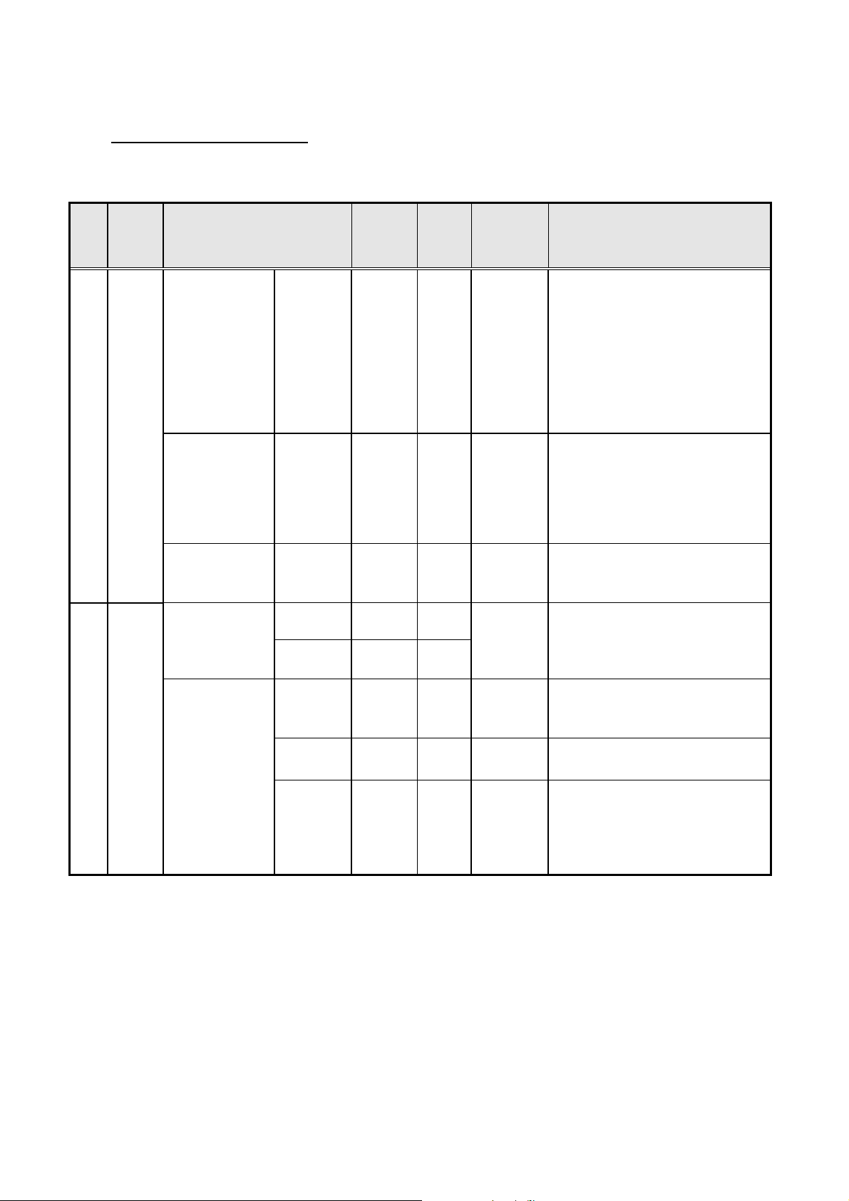
Item NO
Externals
Display panel
Color Grayscale(standard)
BrightNess
Chromaticity
Coordinates
Module size
Weight
Display size
Resolution
Pixel pitch
Sub pixel pitch
White(display load Ratio 100%)
White(display load Ratio 1%,standard)
(x,y)、white 10%
Specification
UC-5X
1 994 × 585 × 66mm
2 16kg
3 921.60 × 522.24mm
(42inch: 16:9)
4 1024 × 1024 pixel
5 0.90(H) × 0.51(V)mm
6 0.30(H) × 0.51(V)mm
7 RGB each color 256 Grayscale
8 140cd/ m2
2
9 (1000) cd/ m
10 (0.300,0.300)
Contrast Contrast in Darkroom(60Hz)
Data signal
Sync Signal
Powersupply
Noise Shade noise at 18dB(A) or less
Guarantee
environment
Video signal (RGB each color)
Dot clock(max)
Horizontal Sync Signal(max)
Vertical Sync Signal
Input voltage/current
Standby electric power(max)
Temperature(operation)
Temperature(storage)
Humidity(operation)
Humidity(storage)
11 (1000:1)
12 LVDS(10bit)
13 52MHz
14 50KHz(LVDS)
15 50Hz ± 1.9 / 60 ± 1.7Hz (LVDS)
16 +3.3/+5/+75-90/+50-65VDC, 0.05/6/4/2A
17 1W
18 25dB(A) or less
19
20
21 20 ~ 85 %RH (no condensation)
22 20 ~ 80 %RH (no condensation)
0 ~ 45 °C
0 ~ 45 °C
*It is made to give priority when there is a delivery specification according to the customer.
– 2 –

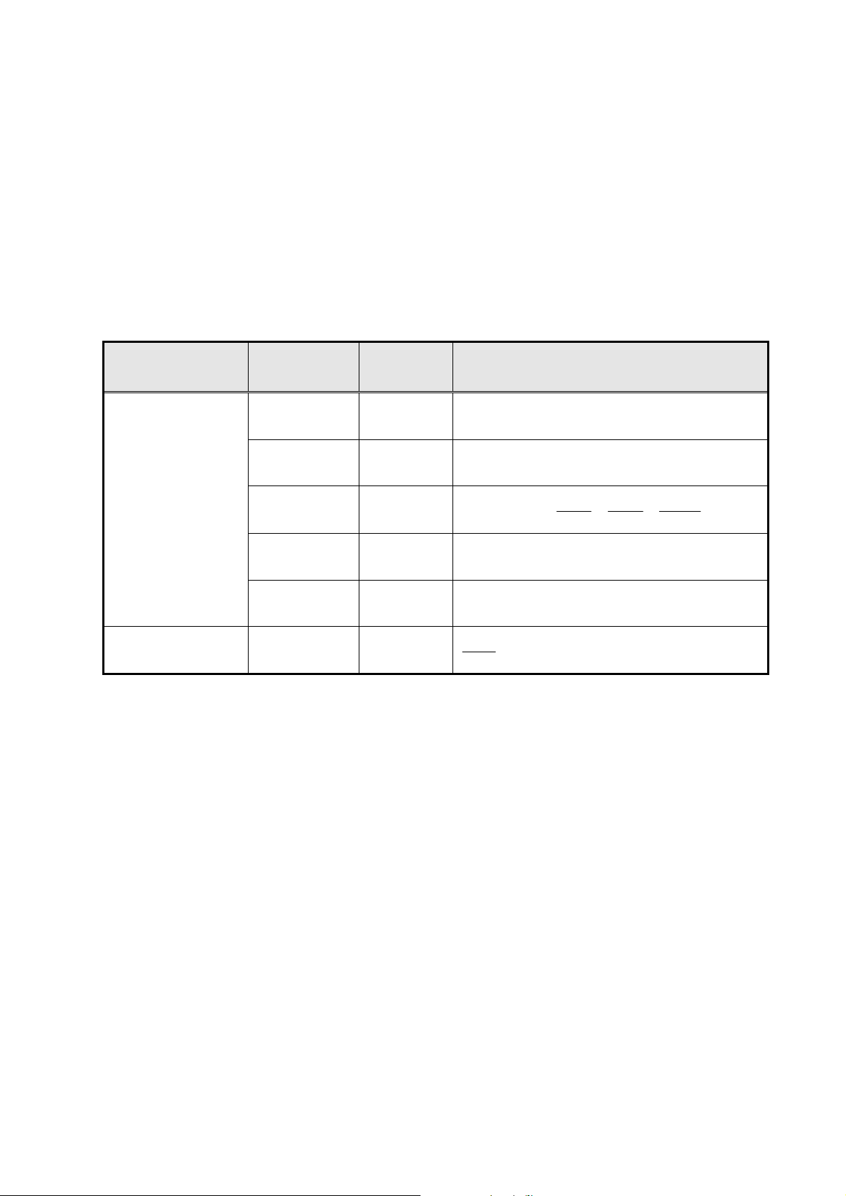
1.3.2
Display quality specification
Non-lighting cell
defect
Non-extinguishing
cell defect
Flickering cell defect
High intensity cell
defect
Item NO
Total number (subpixel)
Density (subpixel/cm2)
Size (H x V) (subpixel)
Total number (subpixel)
Density (subpixel/ cm
Flickering lighting cell defect
(sub pixel/cm
Flickering non-extinguishing cell defect
Twice or more bright point
2
)
2
)
Specification
UC-51 (Standard)
1 15 or less
2 2 or less
(However,1 continuousness or less)
3 1x2 or less, Or 2x1 or less
4
5 Each color 2 cells max
6 5 or less
7 Number on inside of
8 0
6 or less(each color 2 or less)
(
However,1 continuousness or less)
Non-extinguishing cell defect
Brightness variation
Color variation White block of 10% load [9 point]
White block of 10% load [9 point] (%)
In area adjacent 20mm [White] (%)
9 20 or less
10 10 or less
11
X: Average ± 0.015
y: Average ± 0.015
*It is made to give priority when there is a delivery specification according to the customer.
– 3 –
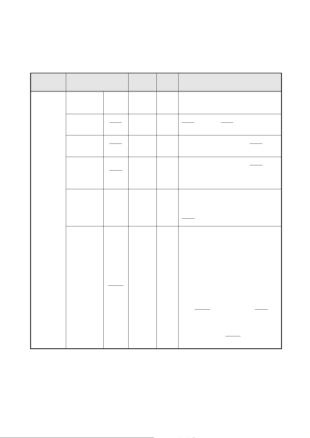
1.3.3
I/O Interface Specification
(1) I/O Signal
No. Item Signal Name
Video Signal
Timing Signal
1
Display data
Clock
RA-
RA+
RB-
RB+
RC-
RC+
RD-
RD+
RE-
RE+
RXCLKIN-
RXCLKIN+
Number
of
signals
1
1
1
1
1
1
1
1
1
1
1
1
I/O Form Content of definition
Differential serial data signal.
Input video and timing signals after
differential serial conversion using a
dedicated transceiver.
The serial data signal is transmitted
seven times faster than the base
signal.
Differential clock signal.
Input the clock signal after
differential conversion using a
dedicated transceiver.
The clock signal is transmitted at
the same speed as the base signal.
Input
Input
LVDS
Differential
LVDS
Differential
Power down
Signal
Communication
2
Control
MPU Communication / Control
PDWN 1 Input LVTTL
SDA 1 I/O
SCL 1 I/O
CPUGO 1 Input LVTTL
PDPGO 1 Input LVTTL
IRQ 1 Output LVTTL
LVTTL
2
(I
C)
Low :LVDS receiver outputs are all
“L”.
High: Input signals are active.
2
I
C bus serial data communication
signal.
Communication with the control
MPU of this product is enabled.
Low power consumption mode of
the control MPU of this product is
released.
“High”: This product is started.
(CPUGO=“High” Effective)
It changes into "Low" → "High"
when this product enters the
undermentioned state.
1. Vcc/Va/Vs output decrease
2. Circuit abnormality detection
– 4 –
(2) LVDS Signal Definition and Function
A video signal (display data signal and control signal) is converted from parallel data to serial
data with the LVDS transmitter and further converted into four sets of differential signals before
input to this product.
These signals are transmitted seven times faster than dot clock signals.
The dot clock signal is converted into one set of differential signals by the transmitter before
input to this product.
The LVDS signal definition and function are summarized below:
Signal name Symbol Number of
Video signal
Timing signal
Transmission line
Clock transmission
line
RA-
RA+
RB-
RB+
RC-
RC+
RD-
RD+
RE-
RE+
RXCLKIN-
RXCLKIN+
signals
1
1
1
1
1
1
1
1
1
1
1
1
Signal definition and function
Display data signal
R2, R3, R4, R5, R6, R7, G2
Display data signal
G3, G4, G5, G6, G7, B2 B4
Display data signal,Sync Signal,Control signal
B4, B5, B6, B7,
Display data signal, Control signal
R8, R9, G8, G9, B8, B9, PARITY
Display data signal, Control signal
R0, R1, G0, G1, B0, B1, N.S
Clock signal
DCLK
Hsync , Vsync ,
BLANK
– 5 –
(3) Video Signal Definition and Function
The table below summarizes the definitions and functions of input video signals before LVDS
conversion.
Item Signal name
Original
Display signal
(before LVDS
transmittance)
Video signal
(digital RGB)
Data Clock
Horizontal
sync signal
Vertical sync
signal
Parity signal
Number
of signals
DATA-R
DATA-G
DATA-B
DCLK
Hsync
Vsync
PARITY 1 Input
10
10
10
1 Input
1 Input
1 Input
Input/
output
Input
Signal definition and function
Display data signal
R9/G9/B9 is the highest intensity bit.
R0/G0/B0 is the lowest intensity bit.
Display data timing signal: Data are read when
DCLK is lowerd. DCLK is continuously
input.
Regulates one horizontal line of data: Begins
control of the next screen when
lowered.
Screen starts up control timing signal: Begins
control of the next screen when
lowered.
Input the same frequency in both
odd-numbered and even-numbered fields.
This signal specifies the display field.
H: Odd-numbered field
L: Even-numbered field
Parity signal should be alternated in every
Vsync cycle.
Hsync is
Vsync is
Display period timing signal.
H indicates the display period and L indicates
the non display period.
Note:
Set this timing properly like followings, as is
used internally for signal processing.
・Set the blanking period so that the number of
effective display data items in one horizontal
Blanking
signal
BLANK
1 Input
period is 1024.
・Set the number of blanking signals in one
vertical period to 512, which is one half the
number of effective scan lines.
If the
BLANK changes when the Vsync
frequency is switched, the screen display may
be disturbed or brightness may change.
The screen display is restored to the normal
state later when the
constant again.
BLANK
length is
*This product does not correspond to the progressive display mode by the parity signal fixation.
When the parity signal is fixed, this product is reversed arbitrarily internally and used.
– 6 –

1.3.4
Connector Specifications
The connector specification is shown below. Please do not connect anything with the terminal
NC.
(1) Signal connector [CN1]
Pin No.
1 RA- 2 GND(LVDS)
3 RA+ 4 SCL
5 RB- 6 GND
7 RB+ 8 SDA
9 RC- 10 GND(LVDS)
11 RC+ 12 CPUGO
13 RXCLKIN- 14 PDPGO
15 RXCLKIN+ 16 IRQ
17 RD- 18 PDWN
19 RD+ 20 GND(LVDS)
Signal name
Pin No.
Signal name
21 RE- 22 GND
23 RE+ 24 GND
25 GND 26 GND
27 GND 28 GND
29 GND 30 GND
DF13-30DP-1.25 V (tin-plated) (Maker: HIROSE DENKI)
[Conforming connector] Housing: DF13-30DS-1.25C
Contact: DF13-2630SCF
(2) Power Source Connectors (PSU only is used on repair working)
(a) Power input connector [CN61]
Pin No.
1 AC(L)
2 N.C
Symbol
3 AC(N)
4 N.C
5 N.C
6 F.G
B06P-VH (Maker: JST)
[Conforming connector]
Housing: VHR-06N(or M)
Contact: SVH-21T-P1.1
– 7 –
(b) Power supply output connector for system [CN62]
Pin No.
Symbol
B03P-VH (Maker: JST)
1 V
2 N.C
3 GND
AUX
[Conforming connector]
Housing: VHR-06N(or M)
Contact: SVH-21T-P1.1
(c) Power supply output connector for system [CN63]
Pin No.
1 Vpr1
2 N.C.
3 Vpr2
4 N.C.
5 GND
Symbol
B5B-XH-A (Maker: JST)
[
Conforming connector]
Housing: XHP-5
Contact:
SXH
(iii) Power Source Connectors
(a) Power supply output connector for system [CN6]
-001T-P0.6
Pin No.
1 Vpr2
2 N.C.
3 GND
4 GND
5 N.C.
6 Vcc
Symbol
B6B-PH-SM3(JST)
[Conforming connector]
Housing: PHR-6
Contact: SPH-002T-P0.5L
– 8 –
(b) [CN23]
Pin No.
1 Va
2 N.C.
3 Vcc
4 GND
5 GND
6 GND
7 N.C.
8 Vs
9 Vs
10 Vs
Symbol
B10P-VH(JST)
[Conforming connector]
Housing: VHR-10N
Contact: SVH-21T-P1.1
(c) Power supply output connector for system [CN7]
Pin No. Symbol Pin No. Symbol
1 N.C. 11 GND
2 N.C. 12 Vra
3 N.C. 13 GND
4 N.C. 14 Vrs
5 GND 15 GND
6 VSAGO 16 Iak
7 GND 17 GND
8 VCEGO 18 Vak
9 GND 19 GND
10 PFCGO 20 Vsk
00 6200 520 330 000 [ZIF Right Angle Connector] (Kyocera elco)
– 9 –

2 SAFETY HANDLING of THE PLASMA DISPLAY
2.1 NOTES TO FOLLOW DURING SERVICING
The work procedures shown with the Note indication are important for ensuring the
safety of the product and the servicing work. Be sure to follow these instructions.
Before starting the work, secure a sufficient working space.
At all times other than when adjusting and checking the product, be sure to turn OFF the
main POWER switch and disconnect the power cable from the power source of the display
(jig or the display itself) during servicing.
To prevent electric shock and breakage of PC board, start the servicing work at least 30
seconds after the main power has been turned off. Especially when installing and removing
the power supply PC board and the SUS PC board in which high voltages are applied, start
servicing at least 2 minutes after the main power has been turned off.
While the main power is on, do not touch any parts or circuits other than the ones specified.
The high voltage power supply block within the PDP module has a floating ground. If any
connection other than the one specified is made between the measuring equipment and
the high voltage power supply block, it can result in electric shock or activation of the
leakage-detection circuit breaker.
When installing the PDP module in, and removing it from the packing carton, be sure to
have at least two persons perform the work while being careful to ensure that the flexible
printed-circuit cable of the PDP module does not get caught by the packing carton.
When the surface of the panel comes into contact with the cushioning materials, be sure to
confirm that there is no foreign matter on top of the cushioning materials before the surface
of the panel comes into contact with the cushioning materials. Failure to observe this
precaution may result in the surface of the panel being scratched by foreign matter.
When handling the circuit PC board, be sure to remove static electricity from your body
before handling the circuit PC board.
Be sure to handle the circuit PC board by holding the such large parts as the heat sink or
transformer. Failure to observe this precaution may result in the occurrence of an
abnormality in the soldered areas.
Do not stack the circuit PC boards.
Failure to observe this precaution may result in problems resulting from scratches on the
parts, the deformation of parts, and short-circuits due to residual electric charge.
Routing of the wires and fixing them in position must be done in accordance with the
original routing and fixing configuration when servicing is completed.
All the wires are routed far away from the areas that become hot (such as the heat sink).
These wires are fixed in position with the wire clamps so that the wires do not move,
thereby ensuring that they are not damaged and their materials do not deteriorate over
long periods of time. Therefore, route the cables and fix the cables to the original position
and states using the wire clamps.
Perform a safety check when servicing is completed.
Verify that the peripherals of the serviced points have not undergone any deterioration
during servicing. Also verify that the screws, parts and cables removed for servicing
purposes have all been returned to their proper locations in accordance with the original
setup.
– 10 –

3 NAME and FUNCTION
3.1 CONFIGURATION
(1) FPF42C128128UC-53 (LOGIC set out left side)
– 11 –

Y
O
O
S
3.2 BLOCK DIAGRAMS
3.2.1
Signal Diagrams
-SUS B.
Y-SUS
POS /NEG
RE
CN31
EVEN SW
Y-SCAN
EVEN SW
Y-SUS
ODD SW
Y-SCAN
ODD SW
ET SW
S
D
M
S
D
M
X-SUS B.
ADM1 ADM2 ADM3 ADM5 ADM6 ADM7 ADM8
ABUSL B
CN51
....
ADM4
ABUSR B.
CN41
X
B
B
X
B
B
X-SUS
X-SCAN
EVEN SW
X-SUS
DD SW
X-SCAN
DD SW
POS
RESET
CN21
SIGNAL
INPUT
CN3
24MHz
CN1
10MHz
OSC
LVDS
I2C
Analog Sw
OSC
DATA PROCESSOR
γ comp.
V-SYNC cont
Failure DET.
FLASH MEMORY
RGB
GAIN
.
SCI.
SCAN CONTROLLER
DITHER
MPU
.
APC cont
I/O
CN7
TIMMING ROM
DATA CONVERTER
SUB FIELD
PRC.
PFCgo
Vsago
Vcego
OSC
80MH
Vrs
Vra
Vrw
Vrx
OSC
40MH
EEPROM
D/A
CN69
LOGIC B.
MEMORY
CONTROLLER
FRAME
MEMORY
PSU B.
CN2
*
CN5
CN4
– 12 –

Y
g
g
V
p
V
p
V
a
s
w
3.2.2
Power Diagrams
-SUS B.
Y-SUS
EVEN SW
Y-SCAN
EVEN SW
Y-SUS
ODD SW
Y-SCAN
ODD SW
POS/NEG
RESET SW
YFVE Vy VE
18V 18V 17V
CONVERTER
CN36
Vcc 5V
Vs 85V
Va 63V
Vw 190V
Vu 55V
DC/DC
S
D
M
S
D
M
CN32
CPUgo
PDPgo
CN52
ADM1
Va 63V
Vcc 5V
Vpr2 3.3V
ABUSR B....
....
Vr
Vr
Vr
Va 63V
Vcc 5V
ADM4 ADM2 ADM5
ADM3 ADM6 ADM7 ADM8
ABUSL B
D/A
MPU
Vcc 5V
Vrst
RST
CN42
CN22
Vxwgo
X
B
B
X
B
B
CN26
X
18V 20V 17V
X-SUS B.
X-SUS
EVEN SW
X-SCAN
EVEN SW
X-SUS
ODD SW
X-SCAN
ODD SW
POS/NEG
RESET SW
DC/DC
CONVERTER
FVE
Vxx VE
DC/DC
CONVERTER
Vcc 5V
Vs 85V
Va 63V
Vx
55V
Vs 85V
AC100
~240V
PFCgo
Vsago
10A
CN61
control
PSU B.
Servce
PFC
Vsago
SW
o
PFC
380V
r2 3.3V
r1 5V
LOGIC B.
CN6
Vsago
Vce
ra
Vcc 5V
63V
5V
CN68
CN64
o
85V
CN23
Vs
85V
*1:Power supply(jig)
– 13 –

3.3 FUNCTION
3.3.1
Logic board Function
(1) Data Processor
- γ adjustment(1 / 2.2 / 2.4 / 2.6 / 2.8)
- NTSC/EBU format(Color matrix) Switch
- RGB gain Control(White balance adjustment, Amplitude limitation)
- Error Diffusion Technology(Grayscale adjustment)
- Dither(Grayscale adjustment)
- Burn-in Pattern generation
(2) Data Converter
- Quasi out-line adjustment (luminous pattern control)
(3) Scan Controller
- Address driver control signal generator(ADM)
- scan driver control signal generator(SDM)
- X/Y sustain control signal generator
(4) Waveform ROM
- Waveform Pattern for drive / Timing memory
(5) MPU
- Synchronous detection
- System control
- Driving voltage(Va, Vs, Vr, Vw) Minute adjustment
- Abnormal watch (breakdown detection)/abnormal processing
- Is(sustain) current control (sustain pulse control)
- Ia(address) current control (sub-field control)
- External communication control
- Flash memory (firmware)
(6) EEPROM
- Control parameter memory
- The accumulation energizing time (Every hour).
- Abnormal status memory (16 careers)
– 14 –
Sub
Address
Data
bit
Symbol Item Function
Setting [hex]
RANGE
INITIAL
value
00 7-0 MAPVER
7 ERRF
01
02 7-0 ERRC ERRor Code
6 OHRF
5 PSDF
4-0 CNDC
address MAP
VERsion
update of
ERRor Flag
update of
Operation
HouRs Flag
Power Shut
Down Flag
CoNDition
Code
Indicates the version number of the
address map.
Indicates that an error has occurred.
It can be cleared with the ErrRST
setting.
If this flag is set, Error code is
written. Cannot enter the PDP-ON
mode.
Indicates that the drive hours are
counted.
Indicates that shutdown of the AC
power is detected and the PDP has
executed the OFF-sequence. It can
be cleared with the PSDRST setting.
Indicates status of the module.
Indicates error code.
The error codes of as many as 16
errors in the past can be retrieved
with the ERRS setting.
code is not stored continuously.
. Same error
00 ~ FF 01
0: Not updated
1: Updated
0: Not updated
1: Updated
0: Not detected
1: Detected
Refer to 4.11.2.6
condition codes.
00~FF 00
0
0
0
Irregular
03 7-0 OHRH
04 7-0 OHRL
Operation
HouRs
Higher bits
Operation
HouRs Lower
bits
Indicates the higher 8 bits of the
module driving hours.
Indicates the lower 8 bits of the
module driving hours.
00~FF 00
00~FF 00
– 15 –

Sub
Address
Data
bit
7 PATSEL
Symbol Item Function
Selecting
patterns
It selects the built-in test pattern
signals of this display. This setting is
valid when the PATON setting is 1.
Setting [hex]
RANGE
0: The single color
display is switched
every 2 seconds. A
total of 8 colors are
displayed.
1:All white (Different
from actual white.)
INITIAL
value
0
20
6 PATON
5 ADEN
4 - -
3 DSPPOL
2 PFCON
1 PDPON
Built-in
pattern
display is set
to ON.
Address
data enable
DiSPlay
POLarity
forcing PFC
ON
High voltage
power supply
ON
Display of the built-in pattern signal
in this product is turned ON/OFF.
The black screen is displayed.
0 is set when the input video signal
has disturbance.
Be sure to use the display with the
setting fixed to 0.
Input reflection polarity setting
When PFCON = 0, If a high voltage
power is switched on, PFCGO is set
high before a high voltage power is
output.
When PDPON = 1, PFCGO is set
high irrespective of the state of a
high voltage power.
Use it for a power control when a
high voltage power is off.
Switches ON/OFF the high voltage
power supply of PDP.
0: Displaying the
input signal
1: Displaying the
built-in pattern
0: Blank
1: Displaying the
input signal
0~1 0
0:Emits light by LOW
1:Emits light by High
0: Power OFF
1: Power ON
0: Power OFF
1: Power ON
0
1
1
0
0
0 DSPBIT Input Data bit Switches 8 bit input / 10 bit input
– 16 –
0: 10 bit input
1: 8bit input
1

Sub
Address
Data
bit
Symbol Item Function
Setting [hex]
RANGE
INITIAL
value
21
7-5 - -
4 CCFMD
3 DCBON
2 PPAON
1 APSON
Color
correction
mode
Dynamic
Color
Balance
Panel Protect
Apc function
Auto Peak
Save
function
Be sure to use the display with the
setting fixed to 0.
Selecting the color correction modes.
Valid when the CCFON setting is 1
Tracking correction of white balance
between the high luminance and the
low luminance.
When a picture with high
luminance/small area is displayed for
about 3 minutes or longer, the
number of pulses is reduced to about
20% at a maximum. This item can be
used to reduce panel
temperature/extend useful life when
the display is used to show a still
image.
If a low display load picture (less
than 2%) is inputted continuously 3
minutes or more, the brightness is
reduced about 50 %.
0~7 0
0:Luminance has
priority.
0
1:Gradation has
priority
0: OFF
0
1: ON
0: OFF
1
1: ON
0: OFF
1
1: ON
22
0 DSETEN
7 CCFON
6 CCFORM
5-3 - -
2-0 GAMSEL
Data
Set
Enable
Color
correction
Color
correction
format
Selecting the
reverse γ
correction
Whether the register value is
reflected to the operating status of
this product, selected by this item.
The following switch is executed.
0:The received register value is
reflected from the next field.
1:The received register value is
stored so that the DSET setting is
reflected from the next field.
(DSET setting: Setting bit 0 of
address FF)
Color collection process is turned
ON/OFF.
Color collection process is switched.
This item is valid when CCFON
setting is 1.
Be sure to use the display with the
setting fixed to 0.
Reverse γ correction level is set.
The setup 7 is the test mode. Do not
select the setup 7.
When the setup 6 is selected, setting
of the addressed in the range of
31~51 become valid.
0: Invalid
1: Valid
0: OFF
1: ON
0: NTSC
1: EBU
0~7 0
0: OFF
1: 1.0 th power
2: 2.2 nd power
3: 2.4 th power
4: 2.6 th power
5: 2.8 th power
6: USER
7: TEST
1
0
0
2
– 17 –
Sub
Address
23 7-0 CONTrast
Data
bit
Symbol Item Function
Peak
luminance
Peak luminance is adjusted.
When the display picture load is
heavy, the peak luminance is
automatically limited.
Setting [hex]
RANGE
00~FF FF
INITIAL
value
24 7-0 R-RATIO R ratio 00~FF FF
25 7-0 G-RATIO G ratio 00~FF FF
26 7-0 B-RATIO B ratio
Clearing the
7 IRQRST
6 ERRRST
5 OHRRST Clearing the
27
4 PSDRST Clearing the
IRQ output
signal
Clearing the
ERRF flag
OHRF flag
PSDF flag
White balance is adjusted.
Use the display with at least one item
being set to FF (hex).
This item implements control to
return the IRQ signal from "HIGH" to
"Low" level when an error occurs.
When this item is set to 1, the IRQ
signal is returned to "Low" level.
This item implements control to
return the ERRF flag to 0 when an
error occurs.
When this item is set to 1, this
setting automatically returns to 0
after returning the ERRF flag to 0.
The control by which the OHRF flag
is returned to 0 is done. This setting
automatically returns to the state of 0
after returning 0 the ERRF flag when
this setting is set to one.
This item exercise control to return
the PSDF flag to 0 when this
machine performs the OFF
sequence at AC power shutdown.
When this item is set to 1, this
setting automatically returns to 0
after returning the PSDF flag to 0.
00~FF FF
0: Normal
1: IRQ signal clear
0: Normal
1: ERRFflag clear
0: Normal
1: OHRF
flag clear
0: Normal
1: PSDF flag clear
0
0
0
0
3-0 ERRS Error code
selection
When this setting is changed and the
ERRC setting is read out, the error
contents (as many as 16 errors) of
the module that have occurred in the
past can be checked.
If more than 16 errors have occurred,
the error code is updated starting
from the oldest error.
– 18 –
0: Latest error
1: Previous error
2:
|
E:
F: Oldest error
0
Sub
Address
Data
bit
Symbol Item Function
Setting [hex]
RANGE
INITIAL
value
7 PWMP
6 - -
28
5-4 PWMAX
3-0
29 7-0
- -
PWM
PASS
Power
Maximam
peek control
Maximum
power
consumption
Password of
peak electric
power setting
The PWMAX setting is switched to
constant brightness (peak electric
power) control. The password setting
is necessary to turn on this setting.
Be sure to use the display with the
setting fixed to 0.
PWMP=0 Setting of the maximum
electric power.
PWMP=1 Setting of peak electric
power. Electric power by
which electric power is
permitted in addition to
improve practical
brightness to the
maximum electric power
set 3:+20W
Be sure to use the display with the
setting fixed to 0.
Password of peak electric power
setting.The password is described to
the delivery specifications. When the
password setting is normally done,
the reading value of the real thing
ground becomes 51.
When password is
set
0:OFF 1:ON
0-1 0
0: -40W
1: -20W
2: ±0W
3: +20W
0: ±0W
1: +20W
2: +30W
3: +40W
0~F 0
51: Permission of
PWMP ON
Another: Prohibition
0
2
FF
Password of
2A 7-0 VRPASS
7-4 - -
2B
3-0 RISTIM RISe TIMe
2C 7-0 PsTPW
2D 7-0 PsTTM
VRPOL
setting
Ps-Tank
PoWer
Ps-Tank
TiMe
If ‘AA” is written, VRPOL setting can
be changed. 00~FF 00
-
Setting of wait time for Vs/Va
stabilization at the time of start up
sequence.
Wait time [ms] = 200×Set value
(Ma x:3000[ms])
The maximum
electric power
setting:
The maximum
over electric
power from +20W
Time which can
operate by the
maximum over
electric power
(*10sec)
When the
amount of an
over electric
power becomes
PsTPW×PsTTM
or less at
PWMP=1, the
control by which
brightness is
lowered is
done.
0~F 0
0~F 5
00-FF 28
00-FF 3C
– 19 –

Sub
Address
Data
bit
Symbol Item Function
Setting [hex]
RANGE
INITIAL
value
7-4 - -
Voltage
30
31 7-0 GAM00
32
33 7-0 GAM01[7: 0]
34
35 7-0 GAM02[7: 0]
36
3 VRPOL
2-0 - -
7-2 - <no use> -
1-0 GAM01[9: 8]
7-3 - <no use> -
2-0 GAM02[10: 8]
7-4 - <no use> -
3-0 GAM03[11:8]
Reference
POLarity
Reverse γ
correction
DC
Reverse γ
coefficient 01
Reverse γ
correction 02
Reverse γ
correction 03
Be sure to use the display with the
setting fixed to C.
Setting of Vrs/Vra output polarity.
Set in the following procedures.
1) Write “AA” in the address 2A.
2) Write “0” or “1” in this address.
3) Write other than “AA” in the
address 2A.
Be sure to use the display with the
setting fixed to 0.
Sets the input level that implements
the forced 0 [LSB] output.
Reverse γ coefficient value is set.
Input Output value of 8 [LSB]
Reverse γ coefficient value is set.
Input Output value of 16 [LSB]
Reverse γ coefficient value is set.
Input Output value of 24 [LSB]
0: POSI
0
1:NEGA
00~FF 1F
00~FF 00
00~FF 04
00~FF 00
00~FF 24
00~FF 00
37 7-0
7-4 - <no use> -
38
3-0
39 7-0
7-5 - <no use> -
3A
4-0
7-1
3B
0
7-5 - <no use> -
3C
4-0
7-1
3D
0 - <no use> -
7-5 - <no use> -
3E
4-0
7-2
3F
1-0
GAM03
GAM04
GAM04
GAM05
GAM05
- <no use> -
GAM06
GAM06
GAM07
GAM07
- <no use> -
[7: 0]
[11: 8]
[7: 0]
[12: 8]
[7: 1]
[12: 8]
[7: 1]
[12: 8]
[7: 2]
00~FF 58
Reverse γ
correction 04
00~FF A7
Reverse γ
correction 05
Reverse γ
correction 06
Reverse γ
correction 07
Reverse γ coefficient value is set.
Input Output value of 32 [LSB]
Reverse γ coefficient value is set.
Input Output value of 40 [LSB]
Reverse γ coefficient value is set.
Input Output value of 48 [LSB]
Reverse γ coefficient value is set.
Input Output value of 56 [LSB]
00~FF 00
00~FF 01
00~FF 12
00~FF 01
00~FF 9A
00~FF 02
00~FF 40
– 20 –

Sub
Address
Data
bit
Symbol Item Function
Setting [hex]
RANGE
INITIAL
value
40
41
42
43
44
45
46
47
48
49
7-5 - <no use> -
[12: 8]
[7: 2]
[13: 8]
[7: 4]
[13: 8]
[7: 4]
[13: 8]
[7: 4]
[13: 8]
[7: 4]
Reverse γ
correction 08
Reverse γ
correction 09
Reverse γ
correction 10
Reverse γ
correction 11
Reverse γ
correction 12
4-0
7-2
1-0 - <no use> -
7-6 - <no use> -
5-0
7-4
3-0
7-6 - <no use> -
5-0
7-4
3-0
7-6 - <no use> -
5-0
7-4
3-0
7-6 - <no use> -
5-0
7-4
3-0
GAM08
GAM08
GAM09
GAM09
- <no use> -
GAM11
GAM11
- <no use> -
GAM11
GAM11
- <no use> -
GAM12
GAM12
- <no use> -
00~FF 03
Reverse γ coefficient value is set.
Input Output value of 64 [LSB]
00~FF 04
00~FF 04
Reverse γ coefficient value is set.
Input Output value of 80 [LSB]
00~FF F0
00~FF 07
Reverse γ coefficient value is set.
Input Output value of 96 [LSB]
00~FF 60
00~FF 0A
Reverse γ coefficient value is set.
Input Output value of 112 [LSB]
00~FF 50
00~FF 0D
Reverse γ coefficient value is set.
Input Output value of 128 [LSB]
00~FF D0
4A
4B
4C
4D
4E
4F
50
51
7-6 - <no use> -
5-0
7-4
3-0 - <no use> -
7-6 - <no use> -
5-0
7-4
3-0
7-6 - <no use> -
5-0
7-4
3-0
7 - <no use> -
6-0
7-5
4-0
GAM13
GAM13
GAM14
GAM14
- <no use> -
GAM15
GAM15
- <no use> -
GAM16
GAM16
- <no use> -
[13: 8]
[7: 4]
[13: 8]
[7: 4]
[13: 8]
[7: 4]
[14: 8]
[7: 5]
Reverse γ
correction 13
Reverse γ
correction 14
Reverse γ
correction 15
Reverse γ
correction 16
Reverse γ coefficient value is set.
Input Output value of 160 [LSB]
Reverse γ coefficient value is set.
Input Output value of 192 [LSB]
Reverse γ coefficient value is set.
Input Output value of 224 [LSB]
Reverse γ coefficient
Input Output value of 256 [LSB]
00~FF 16
00~FF A0
00~FF 21
00~FF E0
00~FF 2F
00~FF 90
00~FF 40
00~FF 00
– 21 –

Sub
Address
Data
bit
Symbol Item Function
Setting [hex]
RANGE
INITIAL
value
E5 7-0 UVrs USER Vrs
E6 7-0 UVra USER Vra
7-3
2 RCLVr
FE
1 EWRVr
0
7-1
FF
0 DSET Data setup
- -
UVrs/UVra
RECALL
UVrs/UVra
Write
- -
- -
Setting Vrs voltage Standard
equation: Vrs=2.99*UVrs/255
Setting Vra voltage Standard
equation: Vra=2.99*UVra/255
Be sure to use the display with the
setting fixed to 0.
Resetting the UVrs, UVra in both of
register and EEPROM to the initial
value by setting RCLVr to 1.
This setting automatically returns to
0 after resetting the UVrs,Uvra.
Storing the UVrs,UVra in register
to EEPROM by setting EWRVr to 1.
This setting automatically returns to
0 after resetting the UVrs,UVra.
Be sure to use the display with the
setting fixed to 0.
Be sure to use the display with the
setting fixed to 0.
When the DSETEN setting is 1,
setting this bit causes all the register
setups that have been set up to now,
to be reflected to the operation status
of this product. They are reflected
from the next field after this bit is
accepted.
00~AA
00~AA
0 0
0:Normal
1: UVrs,UVra
initialized
0:Normal
1: UVrs,UVra
stored in EEPROM
0 0
0 0
0: Normal
1: Execute
Adjusted
in factory
Adjusted
in factory
0
0
0
– 22 –
 Loading...