

Page 1

XS1
RM-Y1011
SERVICE MANUAL
MODEL
KDE-P37XS1
COMMANDER DEST
RM-Y1011 UK
XS1
MODEL
KDE-P42XS1
CHASSIS
COMMANDER DEST
RM-Y1011 UK
KDE-P37/42XS1
- 1 -
RM-Y1011
FLAT PANEL COLOR TV
Page 2

XS1
RM-Y1011
TABLE OF CONTENTS
Section Title Page Section Title Page
Caution ................................................................ 3
Specifications ...................................................... 4
Connectors .......................................................... 5
Self Diagnosis ..................................................... 6
1. GENERAL ................................................................... 7
2. DISASSEMBLY
2-1. Rear Cover Removal ........................................... 21
2-2. Speaker Cover Removal ..................................... 21
2-3. Speaker Removal ................................................ 22
2-4. H1 Board Removal ............................................. 22
2-5. H2 Board Removal ............................................. 23
2-6. H3 Board Removal ............................................. 23
2-7. H4 Board Removal ............................................. 24
2-8. HMP Board Removal ......................................... 24
2-9. U1 Board Removal ............................................. 25
2-10. APS-202 Board Removal ................................... 25
3. SET-UP ADJUSTMENTS
3-1. CVBS PAL System Adjustment ....................... 26
3-2. CVBS NTSC System Adjustment .................... 26
3-3. CVBS SECAM System Adjustment ................. 27
3-4. YC PAL System Adjustment ............................ 27
3-5. YC NTSC System Adjustment .......................... 28
3-6. YC SECAM System Adjustment ...................... 28
3-7. RGB System Adjustment .................................. 29
3-8. YUV System Adjustment .................................. 29
3-9. HDTV Component System Adjustment ............ 30
3-10. White Balance Adjustment ................................. 30
4. DIAGRAMS
4-1. Block Diagrams (1) ............................................ 31
Block Diagrams (2) ............................................ 32
4-2. Circuit Board Location ........................................ 32
4-3. Schematic Diagrams and Printed Wiring
Boards ................................................................. 32
H1 Board Schematic Diagram ............................ 33
H1 Printed Wiring Board .................................. 34
H2 Board Schematic Diagram ............................ 33
H2 Printed Wiring Board .................................. 34
H3 Board Schematic Diagram ............................ 35
H3 Printed Wiring Board .................................. 36
H4 Board Schematic Diagram ............................ 35
H4 Printed Wiring Board .................................. 36
U1 Schematic Diagram ....................................... 37
U1 Printed Wiring Board .................................. 43
N1 Schematic Diagram ....................................... 45
N1 Printed Wiring Board .................................. 46
4-4. Semiconductors .................................................. 47
4-5. IC Blocks ........................................................... 48
5. EXPLODED VIEWS
5-1. Rear Cover and Stand ......................................... 49
5-2. Display Panel, Boards, and Speakers ................. 50
6. ELECTRICAL PARTS LIST .................................. 52
WARNING !!
AN ISOLATION TRANSFORMER SHOULD BE USED DURING
ANY SERVICE WORK TO AVOID POSSIBLE SHOCK HAZARD
DUE TO LIVE CHASSIS, THE CHASSIS OF THIS RECEIVER IS
DIRECTLY CONNECTED TO THE POWER LINE.
SAFETY-RELATED COMPONENT WARNING !!
COMPONENTS IDENTIFIED BY SHADING AND MARKED
THE SCHEMATIC DIAGRAMS, EXPLODED VIEWS AND IN THE
PARTS LIST ARE CRITICAL FOR SAFE OPERATION. REPLACE
THESE COMPONENTS WITH SONY PARTS WHOSE PART
NUMBERS APPEAR AS SHOWN IN THIS MANUAL OR IN
SUPPLEMENTS PUBLISHED BY SONY.
ON
- 2 -
Page 3

CAUTION
Lead Free Soldered Boards
The circuit boards listed below [Table 1] used in these models
may have been processed using Lead Free Solder. The boards are
identified by the LF logo located close to the board designation
e.g. F1, H1 etc [ see examples ]. The servicing of these boards
requires special precautions to be taken as outlined below.
Table 1
XS1
RM-Y1011
example 1
example 2
draoB noitcnuF
1HhctiwS
2HlanimreTtupnI
3HrevieceRRI&DEL
4HDEL
1NrenuTlatigiD
1UoiduA,WSVA,lanimreTtupnI
It is strongly recommended to use Lead Free Solder material in order to guarantee optimal quality of new solder joints. Lead Free Solder is
available under the following part numbers :
rebmuntraP retemaiD skrameR
91-500-046-7mm3.0gK52.0
02-500-046-7mm4.0gK05.0
12-500-046-7mm5.0gK05.0
22-500-046-7mm6.0gK52.0
32-500-046-7mm8.0gK00.1
42-500-046-7mm0.1gK00.1
52-500-046-7mm2.1gK00.1
62-500-046-7mm6.1gK00.1
Due to the higher melting point of Lead Free Solder the soldering iron tip temperature needs to be set to 370 degrees centigrade. This
requires soldering equipment capable of accurate temperature control coupled with a good heat recovery characteristics.
For more information on the use of Lead Free Solder, please refer to http://www.sony-training.com
- 3 -
Page 4

LEDOMMETI metsySnoisiveleT metsySoeretS egarevoClennahC metsySroloC
How to replace the fuse.
Open the fuse compartment with
a screwdriver blade and replace
the fuse.
FUSE
XS1
RM-Y1011
UT-BVD,IoeretSMACIN96B-12B:FHU
)lenaPyalpsiDamsalP(PDP
eziSerutciP
rotcennocoruEnip-12:1
)dradnatsCELENEC(
rotcennocoruEnip-12:2
)dradnatsCELENEC(
rotcennocoruEnip-12:3
)dradnatsCELENEC(
skcaJonohP
tekcoSAICMCP.eludoMsseccAlanoitidnoC
tekcoSMEDOM.noitcennoCmedoM
kcajiniM.rotcennoCesuoMVA
kcajenohpdaeHkcajinimoerets
stupnioiduAskcajonohp
stupnioediVskcajonohp
kcitSyromeMtolSkcitSyromeM
tupnioediVSNIDnip4
]RAER[slanimreTtuptuO/tupnI snoitacificepSlareneG
.BGRrofstupnI
.slangis
.BGRrofstupnI
.oediVSrofstupnI
.slangiS
.tuptuorefooWbuS
]EDIS[slanimreTtuptuO/tupnI lortnocderarfnI:metsyslortnocetomeR
.xorppa(sehcni73:1SX73P-EDK
.)yllanogaidderusaemmc49
.xorppa(sehcni24:1SX24P-EDK
)yllanogaidderusaemmc701
.slangisoediVdnaoiduArofstupnI
oiduAdnaoediVVTfostuptuO
.slangisoediVdnaoiduArofstupnI
dnaoediVelbatceleSrofstuptuO
.ecafretnIkniltramS.slangisoiduA
.slangisoediVdnaoiduArofstupnI
dnaoediVelbatceleSrofstuptuO
ecafretnIkniltramS.slangisoiduA
oiduArofelbairavsrotcennoCtuptuO
LAP
)NIOEDIV(
tuptuOdnuoS
rekaepstfeLdnathgiR)SMR(W51x2
stnemeriuqeRrewoPV042-022
ybdnatS
snoisnemiD
thgieW
/noitpmusnoCrewoP
seirosseccAdeilppuS
serutaeFrehtO
cdV3
stnemeriuqerrewoP
)2(elbaClaixaoC
)1(esuoMVA
noitangisedCEIseirettab2
)AAezis(30R
.ecitontuohtiwegnahcottcejbuserasnoitacificepsdnangiseD
)1SX73P-EDK(W1.2/W513xorppA
)1SX24P-EDK(W1.2/W373xorppA
)1SX73P-EDK(gk0.83xorppA
)1SX24P-EDK(gk5.34xorppA
)1(rednammoCetomeR1101Y-MR
)2(yrettab30RdetangisedCEI
34.4CSTN,85.3CSTN
LM@PM2-GEPM
)1SX73P-EDK(mm682x296x5311xorppA
)1SX24P-EDK(mm682x357x9221xorppA
,CRD,txeteleT,noitpecerlairtserretlatigiD
yromeM,EBBlatigiD,ybloDlautriV,kniltramS
.noitcennocMAC,tamroFotuA,GPE,kcitS
metI
PAPFFOFFO
TAPFFOFFO
CRDNONO
1tracSNONO
2tracSNONO
3tracSNONO
ImroNNONO
LmroNFFOFFO
MmroNFFOFFO
txeteleTNONO
emaNledoM
ytiroirPBGRNONO
)4(nitnorFNONO
rotcejorPFFOFFO
G/BmroNFFOFFO
K/DmroNFFOFFO
SUAmroNFFOFFO
TASmroNFFOFFO
oeretSmaciNNONO
1SX73P-EDK 1SX24P-EDK
WARNING (UK Models only)
The flexible mains lead is supplied connected to a B.S. 1363 fused
plug having a fuse of 5 AMP rating. Should the fuse need to be
replaced, use a 5AMP FUSE approved by ASTA to BS 1362, ie one
that carries the
IF THE PLUG SUPPLIED WITH THIS APPLIANCE IS NOT SUITABLE FOR THE OUTLET SOCKETS IN YOUR HOME, IT SHOULD
BE CUT OFF AND AN APPROPRIATE PLUG FITTED. THE PLUG
SEVERED FROM THE MAINS LEAD MUST BE DESTROYED AS A
PLUG WITH BARED WIRES IS DANGEROUS IF ENGAGED IN A
LIVE SOCKET.
When an alternative type of plug is used, it should be fitted with a
5 AMP FUSE, otherwise the circuit should be protected by a 5AMP
FUSE at the distribution board.
- 4 -
ASA
T
mark.
Page 5
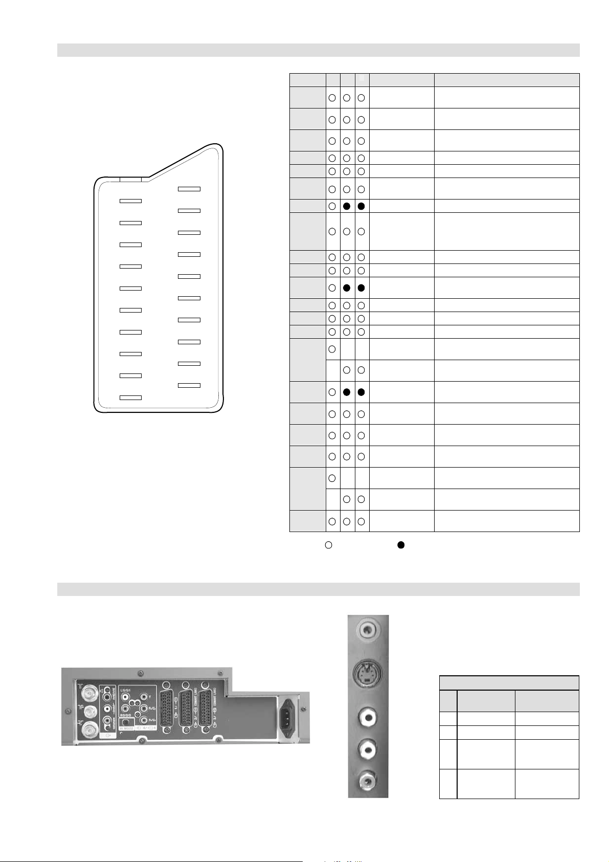
21 pin connector
XS1
RM-Y1011
21
19
17
15
13
11
9
7
5
3
1
20
18
16
14
12
10
8
6
4
2
Pin No 1 2 4 Signal Signal level
1 Audio output B
2
3
4 Ground (audio)
5 Ground (blue)
6 Audio input A
7 Blue input 0.7 +/- 3dB, 75 ohms positive
8 Function select
9 Ground (green)
10 Open
11 Green Green signal : 0.7 +/- 3dB, 75 ohms,
12 Open
13 Ground (red)
14 Ground (blanking)
15
16 Blanking input
17 Ground (video
18 Ground (video
19 Video output 1V +/- 3dB, 75ohms, positive sync 0.3V
20
21 Common ground
3
(right)
Audio input B
(right)
Audio output A
(left)
(left)
(AV control)
_ _ Red input 0.7 +/- 3dB, 75 ohms, positive
_ (S signal Chroma
input)
(Ys signal)
output)
input)
_ _ Video input 1V +/- 3dB, 75ohms, positive sync 0.3V
_ Video input
Y (S signal)
(plug, shield)
Standard level : 0.5V rms
Output impedence : Less than 1kohm*
Standard level : 0.5V rms
Output impedence : More than 10kohm*
Standard level : 0.5V rms
Output impedence : Less than 1kohm*
Standard level : 0.5V rms
Output impedence : More than 10kohm*
High state (9.5-12V) : Part mode
Low state (0-2V) : TV mode
Input impedence : More than 10K ohms
Input capacitance : Less than 2nF
positive
0.3 +/- 3dB, 75 ohms, positive
High state (1-3V) Low state (0-0.4V)
Input impedence : 75 ohms
(-3+10dB)
(-3+10dB)
1V +/- 3dB, 75ohms, positive sync 0.3V
(-3+10dB)
Connected Not Connected (open) * at 20Hz - 20kHz
Rear Connection Panel Side Connection Panel
S-Video
socket
noitarugifnocniptekcosoediVS
niP
oN
1dnuorG-
2dnuorG-
3tupni)langisS(Y,mho57Bd3-/+V1
4tupni)langisS(CBd3-/+V3.0
langiS leveLlangiS
V3.0.cnySevitisop
Bd01+3-
evitisop,mho57
.cnyS
- 5 -
Page 6

XS1
RM-Y1011
XS1 SELF DIAGNOSTIC SOFTWARE
The identification of errors within the XS1 chassis is triggered in one of two ways :- 1: Busy or 2: Device failure to respond to IIC. In the event
of one of these situations arising the software will first try to release the bus if busy (Failure to do so will report with a continuous flashing
LED) and then communicate with each device in turn to establish if a device is faulty. If a device is found to be faulty the relevant device number
will be displayed through the LED (Series of flashes which must be counted).
Flash Timing Example : e.g. error number 3
StBy LED
ON ON
OFF
LED Error Code
DEL
RORRE
EDOC
20rorrEc2I
30rorrErednapxEtroP
40rorrEMORPEE
50)3742S8H(rorrEnoitacinummoCihcatiH
60rorrEkcolCemiTlaeR
70rorrEhctiwSVA
80rorrEhctiwSVUY
90rorrEredoceDamorhCniaM
01)9102AXC(redoceDamorhCretliFbmoCD3
11rorrEretliFbmoCD3
21rorrErenuT
31rorrEFI
41rorrEPSM
51)3612AXC(rorrEredocedamorhCbuS
61)0831ADU(noisrevnoCFIDPSoteugolanA
71)9802AXC(rorrEhctiwSVAbuS
81)4114KA(rorrEnoisrevnoCFIDPSotS2I
91)0246AET(rorrEhctiwSoiduA
02)0515PVT(rorrEredoceDamorhCsaxeT
12gninraWerutarepmeThgiH
22rorrEerutarepmeThgiH
32rorrEnoitcetorPnaF
42rorrEnoitcetorPrekaepS
52detcennoctonelnaClenaP2RM
62rorrEeciveDihcatiH
72tsoLnoirartibrACII
82rorrEeciveDAMME
OFF
NOITPIRCSEDRORRE
- 6 -
Page 7

SECTION 1 GENERAL
a/DIGITAL
XS1
RM-Y1011
DVD
OK
Yes No
automatic tuning?
Do you want to start
Please connect your equipment
according to this chart
on/off button on
most equipment can be connected to more than one type of
TV socket. Once the TV has completed the automatic
tuning process, refer to the ‘Connection Guide’ section on
page 27 for further information on getting the best set up for
The connection diagram should be used as a guide only as
equipment to your TV set. Follow the instructions and press the
OK button to remove the picture and continue the automatic
process.
The first time that the TV set is connected, it is usually
the TV set to turn on the TV.
AC, 50Hz).
Connect the TV plug to the mains socket (220-240V
1
The first time you switch on your TV, a sequence of menu screens appear on the TV enabling you to: 1) check
However, if you need to change any of these settings at a later date, you can do that by selecting the appropriate
how to connect optional equipment to your TV, 2) search and store all available channels (TV Broadcast) and
3) change the order in which the analogue channels (analogue TV Broadcast) appear on the screen.
option in the (Set Up menu) or by pressing the Auto Start Up button on the right side of TV set.
turned on. If the TV is off, press the
2
A diagram appears showing you how to connect a wide range of
3
your equipment.
The Auto Tuning menu appears on the screen. Press the OK button
to select Yes.
4
continued...
Switching On the TV and Automatically Tuning
The operating instructions mentioned here are partial abstracts
from the Operating Instruction Manual. The page numbers of
the Operating Instruction Manual remain as in the manual.
or
OUTIN
VCR
• Use the supplied main lead (Type BF, see page 10).
• Use one of the supplied coaxial cable for aerial connection, and the other one for digital connection.
Connecting the Aerial and VCR
– 7 –
For more details regarding VCR connection, refer to
“Connecting Equipment to the TV” on page 50.
After setting up, secure the TV set to a wall, pillar,
etc, using the supplied anchor attachments, for safety
purposes.
Stabilizing the TV set
of the TV set.
Remove the two screws attached to the upper rear side
1
attachments.
Replace the two screws with the two supplied anchor
2
pillar.
Secure a wall anchor bracket (not supplied) to a solid wall or
3
attachments and then secure to a wall or pillar, etc.
Pass a strong cord or chain through both holes of the anchor
4
Page 8

XS1
5
The TV starts to automatically search and store all available
broadcast channels for you as follows:
a)
The Digital autotune display appears on screen and the search
and store procedure begins. All the available Digital channels
will now be captured and stored. As this may take some time,
a message is included in the display to inform you of the
tuning progress. b)When Digital tuning is complete, the analogue display
appears automatically and the search and store procedure for
the analogue channels begins.
• This procedure could take some minutes. Please be
patient and do not press any buttons, otherwise automatic
tuning will not be completed.
• If no Digital and no Analogue channels were found
during the auto tuning process then a new menu appears
automatically on the screen asking you to connect the
aerial. Please connect the aerial (see page 15) and press
OK. The auto tuning process will start again.
• Once all Digital and Analogue channels have been
captured and stored, the TV returns to normal operation
and displays the first Digital channel tuned.
If no Digital channels are captured, the Analogue channel
that is stored on channel number 1 is displayed.
6
After all available digital and analogue channels are captured and
stored, the Programme Sorting menu automatically appears
on the screen enabling you to change the order in which the analogue
channels are stored.
This menu only appears if the TV has captured analogue
channels.
a)
If you wish to keep the broadcast channels in the tuned order, go
to step 7.
b)
If you wish to store the channels in a different order:
1
Press the
v
or
V
button to select the programme
number with the channel (TV Broadcast) you wish
to move. Press the
b
button.
2
Press the
v
or
V
button to select the new
programme number position for your selected
channel (TV Broadcast). Press the OK button to store.
3
Repeat steps b)1 and b)2 if you wish to change
the order of the other channels.
7
Press the MENU button to remove the menu from the screen.
No channel found.
Please connect aerial
Confirm
Programme Sorting
01020304050607
08
TVE
TVE2
TV3
C33
C27
C58
S02
S06
Programme Sorting
01 TVE
01020304050607
08
TVE
TVE2
TV3
C33
C27
C58
S02
S06
Auto Tuning
The number of stored services 16
0% 100%
Searching. . . 63 %
Press Blue key to cancel Auto Tuning.
Cancel
AutoTuning
Programmes found: 4
Tuning the Digital channels
Tuning the Analogue channels
Your TV set is now ready for use
RM-Y1011
>
ITV
CH4
CH5
BBC1
BBC2
- - - - -
- - - - -
01020304050607
B or b).
Next, press v or V to select an available input signal. Finally press
again the OK button to watch the selected channel.
switched to TV and MENU is switched off, press OK to display a
channel or input signal index. Once you have pressed OK:
screen.
1 W ith t he TV in An alog ue mo de, p ress the OK button to display the “Programme Index table” on
1 To select a channel: press v or V to select a channel and next press
2 a) Displaying a channel or an input signal index: If Media Selector is
again the OK button to watch the selected input signal.
to display the input signal (you can always switch from the channel
index to the input signal index and vice versa by pressing
2 To select an input signal: while watching the channel index, press b
in the list.
c) Store programmes into a list of favourites.
b) Search for a programme quickly by selecting from different categories of programmes.
The “Programme Index table” is only available in Analogue mode.
The ”Programme Index table” is a quick and easy way to search for an Analogue channel (TV Broadcast) or
video input you wish to view.
Selecting Digital or Analogue mode
• Press the DIGITAL button on the remote control to switch to Digital mode.
• Press the button on the remote control to switch to Analogue mode.
The Programme Index table
The Channel Index menu
a) View a complete list of the programmes available for selection, with a preview of the programmes contained
The “Channel Index menu” is only available in Digital mode.
The “Channel Index menu” provides you with a quick and easy way to:
– 8 –
Page 9
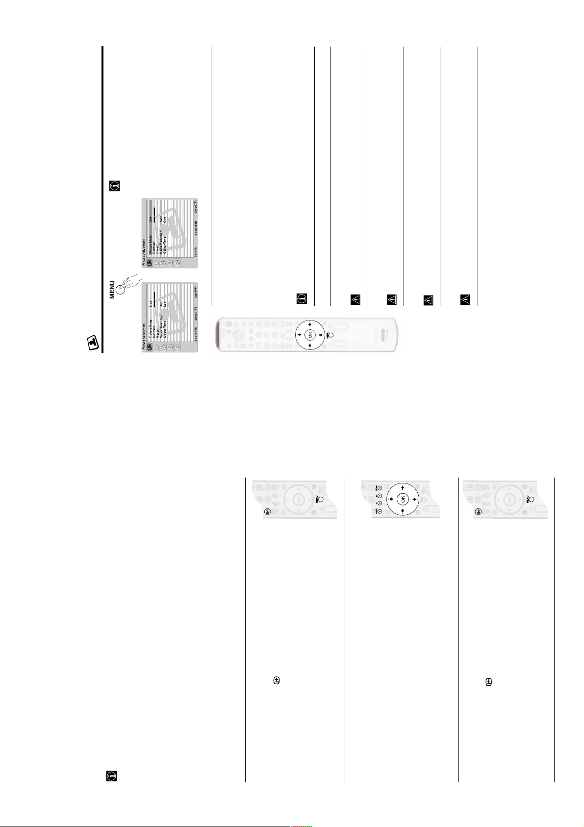
The “Picture Adjustment” menu allows you to
alter the picture settings.
MENU
To do this:
Press the MENU button and then press OK to
Picture Mode: Live
Picture Adjustment
XS1
RM-Y1011
v or V to sele ct the
desired option and press OK. Finally, read below
how to operate into each option.
enter this menu. Next, press
OK
Enter:
Select:Back:
Contrast:
Reset:
Noise Reduction: Auto
Colour Tone: Cool
,
MENU
Exit:
Picture Mode This option allows you to customise the Picture Mode based on the programme
OK
receivers).
V to select:
Live (for live broadcast programmes, DVD and Digital Set Top Box
Movie (for films).
Personal (for individual settings).
or
you are watching. After selecting this option press OK. Next, press repeatedly v
Once you have selected your desired option, press OK to store.
factory to get the best picture quality.
"Brightness", "Colour" and "Sharpness" level of "Live" and "Movie" mode are fixed on the
Contrast Press B or b to reduce or enhance picture contrast. Next, press OK to store.
This option only appears and can only be adjusted if “Picture Mode” is set to “Personal”.
Brightness Press B or b to darken or brighten the picture. Next, press OK to store.
This option only appears and can only be adjusted if “Picture Mode” is set to “Personal”.
Colour Press B or b to decrease or to increase color intensity. Next press OK to store.
This option only appears for NTSC signal (e.g. USA video tapes).
Hue Press B or b to decrease or to increase the green tones. Next press OK to store.
This option only appears and can only be adjusted if “Picture Mode” is set to “Personal”.
Sharpness Press B or b to soften or to sharpen the picture. Next press OK to store.
The Picture Adjustment Menu
Picture Mode: Live
Picture Adjustment
Contrast:
Reset:
Noise Reduction: Auto
Colour Tone: Cool
Select: Enter:
.
b
or
B
/
.
v
or
V
v
/
V
.
.
b
B
Your TV uses an On-Screen Display menu system to guide you through the operations.
Introducing and Using the different Menu systems
This TV has 2 different Menu Systems as follows:
• To navigate through the “Digital Menus”:
some of the screens. For details, please refer to the relevant sections.
• Coloured buttons (red, green, yellow and blue) are basically used to display
• "General TV Menus", press the MENU button.
• "Digital Menus" press the button.
To switch off the:
3
• To enter the selected menu or option, press
• To alter the settings of your selected option, press
• "General TV Menus", press the MENU button.
• "Digital Menus", press the button.
To operate any of the above menu systems, use the following buttons:
To switch on the:
1
system will help you to alter the picture settings, sound settings etc. For more details, please refer to the relevant
sections of the chapter "The General TV Menus" (pages 22 - 32).
programmes currently being shown, etc. This menu also contains a submenu called “Main Menu” which allows
you to customise the Digital side of your TV etc. For more details, please refer to the relevant sections of the
This menu system is available when watching both, Digital and Analogue channels. The displays of this menu
a) "General TV Menus"
b) "Digital Menus"
chapter "The Digital Menus" (pages 33 - 39).
This menu system is only available when watching Digital channels and gives you information on the
• To highlight the desired menu or option, press
• To navigate through the “General TV Menus”:
2
• To confirm and store your selection, press OK.
• To return to the last menu or option, press
– 9 –
Page 10
XS1
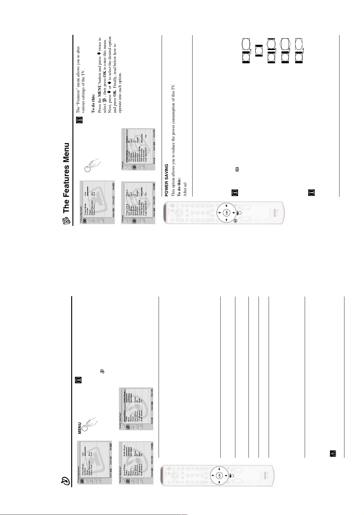
The Sound Adjustment Menu
The “Sound Adjustment” menu allows you to
alter the sound settings.
To do this:
Press the MENU button and press
v
to select
, then press OK to enter this menu. Next,
press
v
or
V
to select the desired option and
press OK. Finally, read below how to opera te
into each option.
Sound This option allows you to customise the Sound Effect. After selecting this
Effect option press OK. Next, press repeatedly
v
or
V
to select:
Dolby* (Dolby Virtual, simulates the sound effect of “Dolby Surround Pro
Virtual Logic”).
Natural (Enhances clarity, detail and presence of sound by using “BBE High
Definition Sound system”**).
Dynamic (“BBE High Definition Sound system”** intensifies clarity and presence
of sound for better intelligibility and musical realism).
Off (Flat response).
Once you have selected your desired option, press OK to store.
Treble Press
B
or
b
to decrease or to increase higher-frequency sounds. Next, press OK to
store.
Bass Press
B
or
b
to decrease or to increase the lower-frequency sounds. Next, press OK
to store.
Balance Press
B
or
b
to emphasise the left or the right speaker. Next, press OK to store.
Reset Press OK to reset the sound to the factory preset levels.
Dual Press
b
. Next:
Sound • For a Stereo broadcast:
Press
v
or
V
to select Stereo or Mono. Next press OK to store.
• For a bilingual broadcast:
Press
v
or
V
to select Mono (for mono channel if available), A (for channel 1) or B
(for channel 2). Next press OK to store.
Auto Press
b
. Next press
v
or
V
to select On (the volume level of the channels will
Volume stay the same, independent of the broadcast signal, e.g. in the case of advertisements)
or Off (the volume level changes according to the broadcast signal). Next press OK to
store.
If you select “Dolby Virtual” on the “Sound Effect” option, the “Auto Volume” option will
automatically be switched to “Off”.
,
m
Sound Adjustment
Sound Effect: Dolby Virtual
Treble:
Bass:
Balance:
Reset
Dual Sound: Stereo
AutoVolume: Off
TV Speakers: Main
Audio Output: Fix
Select: Enter:
OK
Exit:
MENU
Picture Adjustment
Picture Mode: Live
Contrast:
Reset:
Noise Reduction: Auto
Colour Tone: Cool
Select: Enter:
OK
Exit:
MENU
Sound Adjustment
Sound Effect: Dolby Virtual
Treble:
Bass:
Balance:
Reset
Dual Sound: Stereo
AutoVolume: Off
TV Speakers: Main
Audio Output: Fix
Select:Back:
Enter:
OK
MENU
RM-Y1011
The Features Menu
The “Features” menu allows you to alter
various settings of the TV.
MENU
Picture Mode: Live
Picture Adjustment
twice to
v
to select the desired option
V
or
v
to s elec t Reduce. Next, press OK to store.
V
Press the MENU button and press
To do this:
select , then press OK to enter this menu.
Next, press
and press OK. Finally, read below how to
operate into each option.
OK
Enter: :
Select:Back:
Powersaving Reduce
Auto Format On
Film Mode Auto
AV2Output TV
AV3Output TV
SmartLink Output
Connection Guide
RGB Centering
Screen Saver
Logo Illumination Yes
Features
or
v
to select On (if you wish the TV set to
V
or
v
,
MENU
Exit:
OK
m
Contrast:
Reset:
Noise Reduction: Auto
Colour Tone: Cool
Powersaving Reduce
Auto Format On
Film Mode Auto
AV2Output TV
Select: Enter:
AV3Output TV
Features
SmartLink Output
Connection Guide
MENU
Exit:
POWER SAVING
This option allows you to reduce the power consumption of this TV.
To d o th i s:
After selecting the option, press OK. Then, press
AUTO FORMAT
This option allows you to automatically change the aspect ratio of the screen.
To do this:
OK
RGB Centering
Screen Saver
Logo Illumination Yes
Select: Enter:
After selecting the option, press OK. Then, press
pressing repeatedly on the remote control to select one of the following formats:
Even if you have selected “On” or “Off”, you can always modify the format of the screen by
automatically switch the screen format according to the broadcast signal) or Off (if you wish to
keep your preference). Finally, press OK to store.
4:3
SMART
SMART: Imitation of wide screen effect for 4:3 broadcast.
14:9
4/3: Conventional 4:3 picture size, full picture
information.
14/9: Compromise between 4:3 and 16:9 picture size.
WIDE
ZOOM
to adjust the position of the image on the screen (e.g. to read
V
or
v
subtitles).
selected mode.
cut off. Press
• According to the format of diffussion, black bands can always appear whatever the
ZOOM: Widescreen format for letterbox movies.
• In “SMART”, “ZOOM” and “14/9” modes, parts of the top and bottom of the screen are
WIDE: For 16:9 broadcast. Full picture information.
– 10 –
Page 11

XS1
RM-Y1011
continued...
on the programmes currently being shown as well
as the those programmes which are on next.
To do this:
With the TV in Digital mode, press the button
to access this menu. Next read below how to
The “Digital INFO” menu gives you information
operate each option.
button repeatedly until the description for the current
B
button to highlight the language required then press OK to select.
v
or
V
button to highlight the language required then press OK to select.
v
or
V
The Digital INFO Menu
Tue 18 Mar
Channel 5
four times
v
05
15:27
The Wright Stuff
09:05-09:25
Pickid Lake
09:05-09:25
to select the desired option
V
or
v
button. If the programme box is blank, there is no information currently available. To
b
“Off”.
To change channels while the “Digital INFO display” is on screen, press the relevant
numbered buttons on the remote control.
return to the starting point, press the
To do this:
programme reappears.
Press the
DIGITAL INFO DISPLAY
This display gives you a brief description of the next programme in the schedule.
Subtitles Set-upAudio REC
American talk show. Today's guests are sporting a variety of
"faice" books.
Press the button to exit from this display.
9
7
13
46
SUBTITLES
This feature will place Digital subtitles on the screen (similar to selecting p.888 in analogue
Teletext mode).
To do this:
To remove subtitles from the TV screen, access the “Subtitles” pop-up menu and select
pop-up menu. Press the
With the “Digital INFO display” on the TV screen, press the RED button to access the “Subtitles”
Press the button to exit from this menu.
AUDIO
This feature allows you to listen to the broadcast in different languages when the programme is
broadcast in multiple languages.
To do this:
Press the button to exit from this menu.
With the “Digital INFO display” on the TV screen, press the GREEN button to access the “Audio”
pop-up menu. Press the
The Set Up Menu
The “Set Up” menu allows you to alter various
options on this TV.
MENU
Picture Mode: Live
Picture Adjustment
and press OK. Finally, read below how to
operate into each option.
to select , then press OK to enter this menu.
Next, press
To do this:
Press the MENU button and press
OK
Enter:
Select:Back:
AutoTuning
Programme Sorting
Programme Labels
AVPreset
Manual Programme Preset
Set Up
,
MENU
Exit:
OK
m
AutoTuning
Programme Sorting
Programme Labels
AVPreset
Contrast:
Reset:
Noise Reduction: Auto
Colour Tone: Cool
Select: Enter:
Manual Programme Preset
Set Up
MENU
OK
Enter:
Select: Exit:
AUTO TUNING
This option allows you to automatically search for and store all available TV channels.
To do this:
After selecting the option, press OK and then proceed in the same way as in the steps 4 and 5 of
the section “Switching On the TV and Automatically Tuning” on pages 16 and 17.
PROGRAMME SORTING
This option allows you to change the order in which the channels (TV Broadcast) appear on the
screen.
To do this:
After selecting the option, press OK and then proceed in the same way as in the step 6 of the section
“Switching On the TV and Automatically Tuning” on page 17.
– 11 –
Page 12
XS1
RM-Y1011
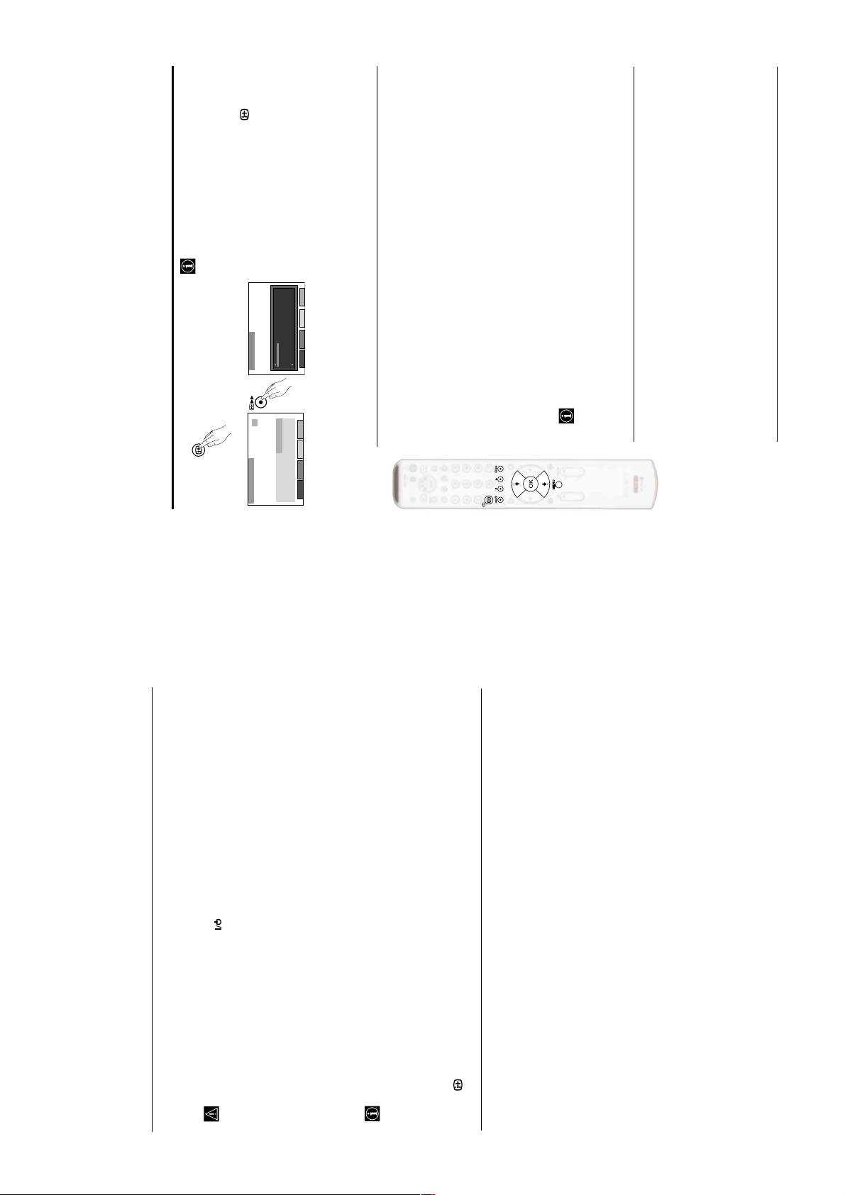
allow you to customise the Digital side of your
TV.
This menu contains several features that will
To do this:
With the TV in Digital mode, press the button to
access the “Digital INFO display” on the TV screen,
then press the BLUE button to access the “Set-up”
(“Main Menu”). Next read below how to operate each
option.
Exit
Main Menu
Favourite Programme
Wallpaper
Parental Control
Auto Tuning
Detail Set-up
CAM Set-up
Digital Set-up
15:27
Tue 18 Mar
Press OK key to enter.
• Press the YELLOW button if you wish to delete (clear) all favorite settings
3 When you have found and highlighted a programme you want to register as a favourite, press
• Press the OK button again to cancel your selection.
“Wallpaper” then press the OK button to display the “Wallpaper” menu.
the OK button. A tick appears alongside that programme in the display.
4 Repeat steps 2 and 3 to store other programmes as favourites.
5 Press the BLUE button to return to the “Main Menu”.
WALLPAPER
This option allows you to customise the background pattern of the Digital menus.
To do this:
the OK button to store.
1 Once you have entered into the “Main Menu”, press the V or v button to highlight
2 Press the V or v button to select your choice of wall paper (4 different choices) followed by
3 Press the BLUE button to return to the “Main Menu”.
05
FAVOURITE PROGRAMME
This option allows you to store your favourite channels (TV Broadcast) in a list for quick access.
The Wright Stuff
09:05-09:25
To do this:
Set” menu.
“Favourite Programme” then press the OK button to display the “Favourite Programme
1 Once you have entered into the “Main Menu” press the V or v button to highlight
favourite is highlighted. If you do not wish to select one of these channels as a favourite, press
the RED or GREEN button to display the previous or next 5 channels in the list.
2 Press the V or v button to scroll through the list until the channel you wish to store as a
BLUE
The Digital Set-up Menu
Channel 5
Subtitles Set-upAudio REC
American talk show. Today's guests are sporting a variety of
"faice" books.
Pickid Lake
09:05-09:25
REC
This feature allows you to automatically record on your VCR the selected programme*.
*Only for SmartLink VCRs.
programme being recorded, press the TV button on the remote control to switch the TV into standby
mode.
the recording will be cancelled.
that a programme has been set to be recorded.
• Do not switch off the TV once a programme has been set to record. If you do not wish to view the
• With the TV in standby mode, the standby indicator will flash green and red periodically to remind you
• Do not change channels or switch the TV to analogue mode once a programme has started recording or
To d o th i s:
With the “Digital INFO display” on the TV screen, press the YELLOW button to access the “REC” pop-up menu.
If you highlight a future programme, the Timer feature allows you to automatically set your VCR to record
Press the RED button and your VCR will automatically record the selected programme when it starts (only
the selected programme, or have the TV switch to the correct channel automatically when the selected
programme starts.
if your VCR has SmartLink facility), or press the GREEN button if you wish the programme to appear on
your TV screen when transmission begins.
If your VCR does not have SmartLink, a message is displayed reminding you to manually set your VCR. Press
the RED button to continue or press the BLUE button to return to the INFO display.
Press the button to exit from this menu.
– 12 –
Page 13

XS1
RM-Y1011
v or V buttons. Once the two
Analogue Teletext
screens are overlapped, they can be swapped by
pressing the OK button.
screen by pressing
the teletext service you wish to view.
(PAT) mode. The screen is divided into two with the
Text display on the left and the TV channel in the
bottom right corner.
1 Select the Analogue broadcast channel which carries
2 Press the button once to enter Picture And Text
To switch on Teletext :
service (usually page 100) gives you information on how to use the service. To operate teletext, use the remote
control buttons as indicated below.
Teletext is an information service transmitted by most Analogue TV stations. The index page of the teletext
Teletext errors may occur if you use a channel (TV Broadcast) with a weak signal.
to select “Detail Set-up”
v
or
V
While viewing PAT, you can zoom the picture
9
7
13
46
the button a second time.
3 If you wish to view the Text in full screen mode, press
To select a Teletext page:
is not available. If this is the case, input another page number.
Input 3 digits for the page number, using the numbered buttons.
• If you make a mistake, retype the correct page number.
• If the counter on the screen continues searching, it is because the page
To access the next or preceding page:
Press PROG + ( ) or PROG - ( ) .
To freeze a teletext page:
Press / . Press it again to cancel the freeze.
To select a sub page:
button to highlight
v
or
V
B or b.
the bottom of the teletext page. Press the appropriate coloured button (red, green, yellow
or blue) to access the page corresponding to your menu choice.
Fastext service lets you access Teletext pages with one button push.
When you are in Teletext mode and Fastext is broadcast, a colour coded menu appears at
A teletext page may consist of several sub pages. In this case, one or more arrows appear next
showing the number of sub pages contained on this page. As soon as sub pages are available, they
start to automatically run. If you want to stop the show and select your desired sub page, press
repeatedly
to the page number. Press B or b to display an information line at the bottom of the screen
button to
b
To Switch Off Teletext:
Fastext
Press .
customise your TV.
The “Detail Set-up” menu allows you to further
and press the OK button. Next read below now to
To do this:
With the TV in Digital mode, press the button.
05
The Wright Stuff
09:05-09:25
15:27
Tue 18 Mar
Subtitles Set-upAudio REC/Timer
American talk show. Today's guests are sporting a variety of
"faice" books.
Channel 5
Ricki Lake
The Digital Detail Set-up Menu
09:05-09:25
operate each option.
Next press the BLUE button to access the “Main
Menu”. Then press
Detail Set-up
Manual Tuning
PIN Code
Software Download
System Information
Press OK key to enter.
BLUE
Main Menu
Favorite Programme
Wallpaper
Parental Control
Auto Tuning
Detail Set-up
CAM Set-up
Press OK key to enter.
Back
Exit
MANUAL TUNING
This option allows you to select a channel number from the displayed list and change the digital
services of that channel.
– 13 –
To do this:
button to highlight the chosen channel number for your new channel. If you
v
or
V
“Manual Tuning” then press the OK button to display the “Manual Tuning” menu.
do not wish to select any of the programme numbers listed, press the RED or GREEN button
Once you have entered into the “Detail Set-up” menu, press the
1
to display the previous or next 5 programme numbers on the list.
Press the
2
With your channel number highlighted, press the OK button to display the “Manual
Programme Search” screen.4Press the
3
button to begin the search process. The words “Searching Down” or
button if you wish to change the channel number, then press the
v
v
or
or
V
V
make the select search box active.
Press the
“Searching Up” appear in the select search box to indicate that the TV is searching. If no
Digital services are found on the channel you have chosen, the channel number changes up or
5
button to find and highlight the service you wish to allocate to the channel
v
or
V
Press the
down automatically and the search continues. When all services allocated to the selected
channel have been found, the service selection screen is displayed.
Repeat Steps 2 to 6 if you wish to manually add more channels to your TV. 8Press the BLUE button to return to the “Digital Set-up” menu.
number selected in Step 2, then press the OK button to display the channel selection screen.
6
7
Page 14

EPG
XS1
RM-Y1011
continued...
buttons to move left and
B
buttons to move the
v
or
b
or
V
on the remote control.
The EPG menu (Electronic Programme Guide) is an onscreen
electronic programme guide that provides you with a quick and easy
way to: View a complete list of the programmes available with a
preview of the programmes currently being broadcast, reduce the
size of the list by selecting a category of programme, e.g. Sports or
Movies, and record programmes.
To do this:
With the TV in Digital mode, press the button to access to the
Pet Rescue
Countdown
By The Light of The Silvery Moon
Fifteen to One
Watercolour Chal
i
i
04 Channel 4
05 Channel 5
EPG. Next read below how to operate each option.
LIST OF PROGRAMMES
This screen consists of an information window, a preview window, a 2 hour timer bar (divided
into 30 minute intervals) and a 5 channel programme list covering the 2 hour period. You can
select different programmes to get information.
Previous Timer ListCategoryNext
DIGITAL
To do this:
button once more after highlighting the last programme on the right,
b
buttons to highlight the category you want, then press the OK button. The
v
or
V
For information on the types of Categories along with instructions on how to add and
remove programmes from the Favourite list, please refer to “The Channel Index menu”
right. If you press the
coloured cursor bar up or down the programme list and the
the programmes scheduled for the next 2 hour period are displayed.
As each programme is highlighted, a brief description of the programme appears in the event
information box at the top left of the screen.
If you do not wish to select a programme from the 5 channels listed, press the GREEN button
to display the next 5 channels or RED button to display the previous 5 channels.
preview in the preview window. If you have previously set a viewing age limit in the
“Parental Control” option (see page 36), and the programme exceeds that age limit, you will
be asked to enter your PIN code before the preview is allowed.
With the EPG menu on screen by pressing , press the
1
If a programme you highlight is currently being broadcast, press the OK button to obtain a
2
to exit the EPG menu and view the programme at full size.
When the programme in the preview screen is the one you wish to watch, press the button
3
THE CATEGORY POP-UP LIST
The “Category” pop-up list allows you to quickly search for a programme by choosing from
different categories of programmes. For example, select the “News” option from the “Category”
With the EPG menu on screen by pressing , press the YELLOW button to display the
Press the
EPG programme list will now only contain programmes of the type selected.
“Category” pop-up list.
pop-up list to display programme information only for News channels.
To do this:
1
2
section of this instruction manual on page 18.
• The EPG menu is only available when watching Digital channels.
• If the TV is not already in Digital mode, press the DIGITAL button
BykerGrove
Celebrity!
16:30
Sabrina, The Teen
16:00
Snooker
Rugrats why5 New
collect, tame and train the wild Pokemon and earn the
title Pokemon Master
Max Steel
15:30
Pokemon
Tweenies Ar thur
15:00
Press i+ key to continue,
OK key to preview.
01 BBC ONE
02 BBC TWO
03 ITV Channel 3
Tue 18 Mar
15:27
All category
15
03 ITV channel 3
Pokemon
15:35 – 16:00 Tue 28 Nov
The adventures of 10-year-old Ash in his quest to
• The “Digital Teletext” is only available when watching Digital channels.
Digital Teletext
09:07 18 Mar
Press BLUE to change section.
B B C SHOURTCUTS CHANGE TV BACK MENU
Entertainment News
Lottery
Films
Soups
Singles and Albums Charts
Web Guide
On This Day
Entertainment
B
,
v
,
V
buttons to select the symbol then press
b
or
B
,
v
,
buttons (to move around the screen),
b
and
B
,
v
,
V
• The OK button (to select items on screen),
• The button (to cancel a selection or exit Digital Teletext),
• The button to load and exit Digital Teletext.
This Digital service includes high quality text and graphics along with advanced navigation options.
For example, Digital Text from the BBC may look different to Digital Text from ITV which may use
• If the TV is not already in Digital mode, press the DIGITAL button on the remote control.
• Many Digital broadcasters now provide a Digital Teletext service in the form of a dedicated Teletext channel.
different navigation methods.
• The appearance, content and navigation methods of all Digital Text services are decided by the broadcaster.
•The
buttons:
• Most of the Digital Text services currently available use simple navigation methods based on the following
With the TV in Digital mode, press . Next press the numbered
buttons on the remote control to select a dedicated Teletext
channel number. To find out the channel number of a dedicated
Digital Teletext channel, use the “Channel Index menu”. (Please
refer to “The Channel Index menu” section of this instruction
manual, on page 18)
Dedicated Digital Teletext channels
1
• The four coloured buttons (to access shortcuts).
DIGITAL
9
-/--
7
13
46
Instructions on-screen will tell you how to change the
displayed programme.
On some pages the TV programme is also displayed.
Normal Teletext services may also be available on other Digital
instructions to access the required information.
Once the Teletext channel is displayed, follow the on-screen
2
“OK” or “Cancel”, press the OK button for “OK” and the
If when viewing the Teletext pages, you are requested to select
3
button to exit.
button for “Cancel”.
When you have finished viewing Teletext, press again the
4
channels. Sometimes this is indicated by a small symbol or text
Selecting Teletext from other Digital channels
V
buttons, the coloured buttons and/or the numbered buttons to
display on your TV screen, superimposed on the channel you are
watching.
Press the
Alternatively, you may be requested to use the numbered and
the OK button to display the chosen information.
coloured buttons on your remote control to display the various
pages of text information. If when viewing the teletext pages, you
are requested to select “OK” or “Cancel”, press the OK button for
1
2
b
Once the text information is displayed on screen, use the
“OK” and the button for “Cancel”.
3
When you have finished viewing Teletext, press the button
or
access the chosen information.
and then select an alternative Digital channel.
4
– 14 –
Page 15
XS1
RECORDING PROGRAMMES
To select a programme for recording or timed display:
1
With the EPG menu on screen by pressing , press the
V
,
v
,
B
or
b
buttons to highlight a programme in the
EPG menu that you wish to record, then press the OK button. The Timer screen appears.
2
Press the RED button and your VCR will automatically record the selected programme when it starts (only if
your VCR has SmartLink facility), or press the GREEN button if you wish the programme to appear on your
TV screen when transmission begins.
• If you do not have a SmartLink VCR, a message appears on screen to inform you. Press the RED button
to store the programme settings on the TV, then set the timer recording function on your VCR to
correspond with the programme you have stored for recording.
• When a programme has been stored for recording, a solid bar appears in the EPG display directly
under the timer bar. This solid bar sh ows you the a mount of time allocated t o a rec ording, and remind s
you that you are unable to record any other programmes during that period of time.
To set the Manual Timer:
1
With the EPG menu on screen by pressing , press the BLUE button to display the Timer List menu. 2Press the RED button.
If your VCR does not have SmartLink a message will be displayed reminding you to set your VCR
timer.
3
Press the
V
or
v
buttons to select the correct date. Press the
b
button to highlight the start time.
4
Press the
V
or
v
buttons to select the start time. Press the
b
button to highlight the stop time.
5
Press the
V
or
v
buttons to select the stop time. Press the
b
button to highlight the programme.
6
Press the
V
or
v
buttons to select the programme. Press the OK button to store. The Timer List menu is
displayed. The event is now set to the Timer List. Press the YELLOW button to delete the timed event or press
the BLUE button to return to the main EPG screen.
7
Press the RED button and repeat steps 3 to 6 if you wish to store further programmes for recording. 8Press the button to return to normal TV operation. 9If you have selected to record the event onto a VCR, set the timer recording function on your VCR to switch on
and off to correspond with the programmes you have stored for recording.
• Once a programme has started recording, do not switch channels or the recording will be cancelled.
• When a programme has been set to record and the TV is in standby mode, the standby indicator on the
front of the TV will flash green and red periodically to remind you that a programme has been set to
record.
To cancel a previously set event:
1
With the EPG menu on screen by pressing , press the BLUE button to display the Timer List.2Press the
V
,
v
,
B
or
b
buttons to highlight the programme/event you wish to cancel.
3
Press the YELLOW button to cancel the programme/event.
RM-Y1011
equipments may not be
displayed on this
television screen.
precautions, we
recommend that you
carefully read the
instructions supplied
with the "Memory
Stick".
non-Sony brand "Memory Stick" media, it is
possible that some images cannot be displayed and
some features (rotate, etc.) may not be available. If
you attempt any of these operations an error message
• Pictures taken by s ome
• In addition to these
v facing front and
• Although you may be able to view images on certain
will occur.
A "Memory Stick"* is a new recording medium with a data capacity that exceeds a floppy disk. It is specially
designed for exchanging and sharing digital data among "Memory Stick" compatible products. With this TV
About "Memory Stick"
you can use the "Memory Stick" to display still images JPEG pictures, DCF version 1.0 format)** as well as
moving pictures (MPEG 1).
etc. It is supported by Sony and other manufacturers.
* "Memory Stick" and the logo are trademarks of Sony Corporation.
** DCF (Design rules for Camera File systems) is a standard file name format for digital still cameras, DV camcorders
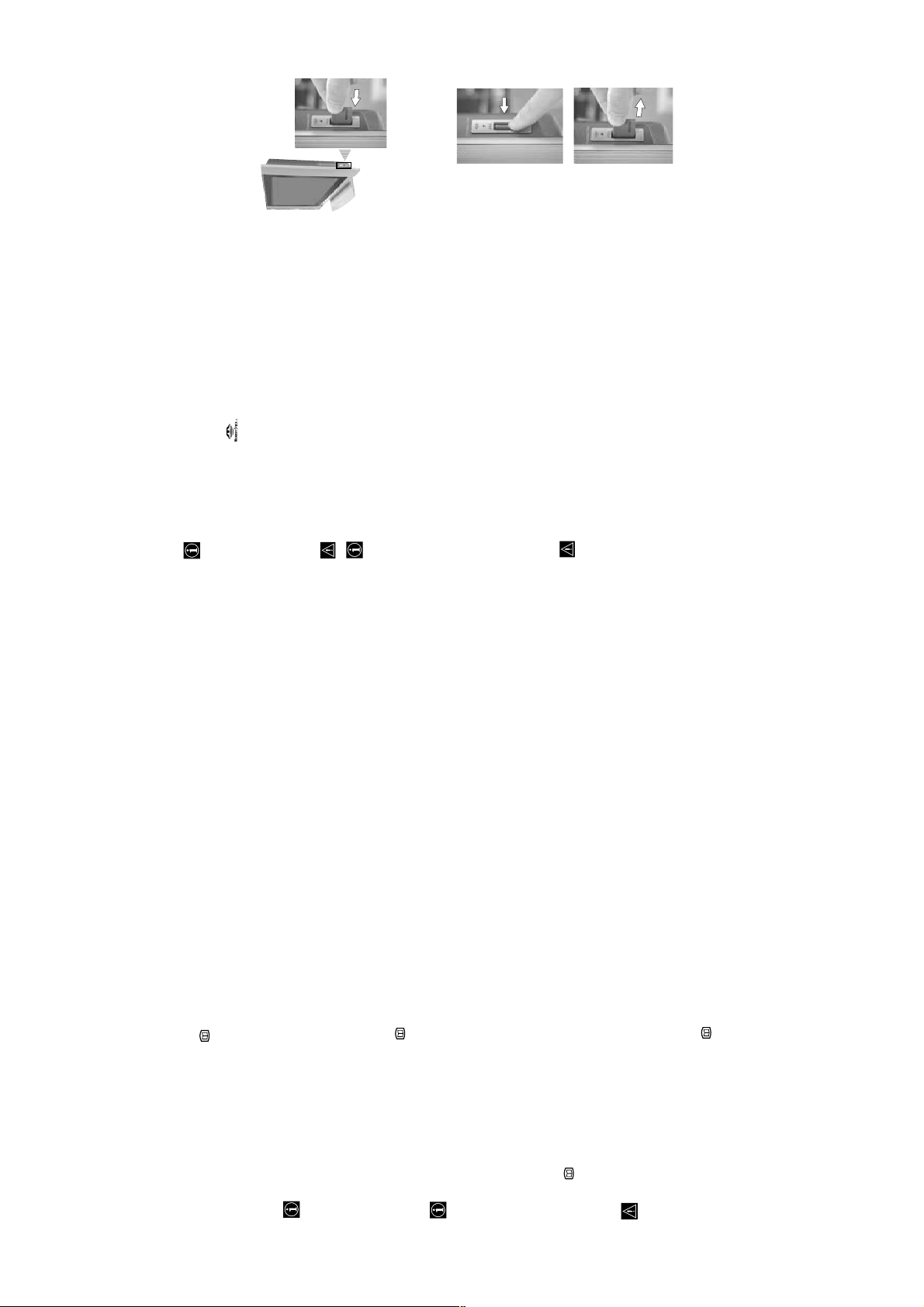
Inserting a "Memory Stick"
pointing towards the "MEMORY STICK" slot.
The red light of the Memory Stick flashes indicating that the
"Memory Stick" contents are being read.
Insert the "Memory Stick" with the mark
Insert a "Memory Stick", into the “MEMORY STICK” slot until it
clicks into the connector (see picture).
Inserting a "Memory Stick Duo"
You can also use a "Memory Stick Duo" with this TV by inserting the "Memory
Stick Duo directly into the "MEMORY STICK" slot.
Viewing pictures or movies from the "Memory Stick"
See pages 45-49.
Removing a "Memory Stick"
Push the "Memory Stick" and then release, the "Memory Stick" will spring out.
"Memory Stick" precautions
reading or writing data.
important data that you record on the "Memory
Stick".
Remove the "Memory Stick".
• Do not remove the "Memory Stick" while it is
prevention switch to "LOCK", data cannot be
• We recommend that you make a backup copy of
• When you set the "Memory Stick" erasure
while it is reading or writing data.
- you remove the Memory Stick or turn off the TV
to the effects of static electricity or electric noise.
- you use the "Memory Stick" in a location subject
only. Any files not recognised as DCF format will
be displayed as “--------” or in blank. JPEG DCF
formatted files that have been created or modified on
a PC may not appear correctly on the TV screen.
• "Memory Stick" supports JPEG DCF formatted files
recorded, edited, or erased.
• Data may become damaged if:
– 15 –
Page 16

XS1
Connecting a DVD or DVD recorder
Connect the DVD or the DVD recorder to the Scart connector
2/
J.
Connecting a DVD recorder with 576p signal format
Some DVD recorder may have 576p signal format. In this case, connect the DVD recorder to the Scart connector
2/
J, to the audio input jacks 4 G and to the video component jacks Y, P
B
/C
B
, P
R
/C
R
4 H.
Using this connection, the TV will record from the AV2 input ( Scart connector
2/
J).
To watch the input signal, you can chose from AV2 (Scart connector
2/
J) or AV 4 (audio input jacks
4 G and video component jacks 4 H). To watch the best picture we recommend you select AV 4 .
Connecting Audio Equipment to the TV
To listen to the sound from TV on Hi-fi equipment.
Connect your audio equipment to the audio output sockets E if you wish to amplify the audio output from the TV.
Next, using the menu system, select the “Sound Adjustment” menu and set the “TV Speakers” to "Off" (see page 25).
• To control the external speakers using this remote control, set “Audio Output” option to “Variable” in
the “Sound Adjustment” menu (see page 25).
• The volume of the external speakers can be altered by pressing the volume buttons on the TV remote control.
The treble and bass setting can also be altered through the “Sound Adjustment” menu (see page 24).
For a sub woofer
Connect your sub woofer to the 5 W/G/W/G output jack D using a monaural audio cable.
To enjoy “Dolby Virtual” sound effect through your
audio equipment
Place the speakers of your equipment in front of your listening position and
beside the TV set.
Then by using the menu system, select the menu “Sound Adjustment”. Next
set the option "Audio Output" to "Variable" and the option "Sound Effect" to
"Dolby Virtual" (see pages 24 and 25).
To control the volume level of an external amplifier
When you connect the AV mouse and install it in an external amplifier, you can use the external amplifier’s remote
control toward the TV for controlling the volume level of the external amplifier. Connect the AV mouse to the AV
MOUSE IN jack F, and install it right above the external amplifier’s remote control sensor.
AV mouse
(supplied)
Amplifier
Remote control sensor
Your sitting position
~50°
Hi-Fi speakers
RM-Y1011
VCR
Decoder
K
J
I
H
G
D
DVD
n
o
i
t
2
a
t
S
y
a
l
P
F
E
Computer
a product of Sony
Entertainment,
Inc.
a trademark of
Sony Computer
Entertainment,
“PlayStation” is
*
“PlayStation”*
DVD recorder with
component signal format
Inc.
“PlayStation” is
*
Compact AV
System/Amplifier
S
S
continued...
Hi-fi
Sub woofer
S VHS/Hi8/
DVC
camcorder
(MONO)
B
A
• Using the following instructions you can connect a wide range of optional equipment to your TV set.
• Connecting cables are not supplied.
Connecting Equipment to the TV
C
– 16 –
same time.
To avoid snowy picture, do not
connect external equipment to
8mm/Hi8/
DVC
connectors A and B at the
information on SmartLink, please refer to the instruction manual of your SmartLink VCR/DVD recorder.
camcorder
Connecting a VCR
SmartLink is a direct link between the TV set and a SmartLink compatible VCR/DVD recorder. For more
Connecting a VCR or a DVD recorder that supports SmartLink
If you use a VCR or a DVD recorder that supports SmartLink, please connect the VCR or the DVD recorder to the
To connect a VCR, please refer to the section “Connecting the aerial and VCR” of this instruction manual on page 15.
connect a VCR or a DVD recorder to both Scart connectors, select which Scart supports SmartLink through
the “SmartLink” option in the “Features” menu. For details see page 26.
Both Scart connectors 2/ J and 3/ K cannot support SmartLink at the same time. If you
TV using a Scart lead to the Scart 2/ J or 3/ K.
Page 17

XS1
G
G
RM-Y1011
X
U
X
U
A
D
V
D
V
fig. 1
T
MODE
R
C
V
A
D
V
D
V
T
fig. 3
MODE
R
C
V
6 sec.
041, 042, 043, 044, 053, 054, 055
Remote Control Configuration for VCR or DVD
button until the green light iluminates according to
t
SONY 001, 029, 030, 036, 037, 038, 039, 040,
AIWA 021
AKAI 032
DENON 018, 027, 020, 002
GRUNDIG 009, 028, 023, 024, 016, 003
HITACHI 025, 026, 015, 004, 035
JVC 006, 017
KENWOOD 008
LG 015, 014, 034
LOEWE 009, 028, 023, 024, 016, 00 3
MATSUI 013 , 016
ONKYO 022, 033
PANASONIC 018, 027, 020, 002, 045, 046, 047
PHILIPS 009, 028, 023, 024, 016, 003, 031
PIONEER 004, 050, 051, 052
SAMSUNG 011, 014
SANYO 007
SHARP 019, 027
THOMSON 012
TOSHIBA 003, 048, 049
YAMAHA 018, 027 , 020, 002
or
T
button on the remote control for approximately 6
T
light (according to your selection) will be lit momentarily (see fig.
3), otherwise repeat all the above steps.
On those brands that have more than one code, enter the first code number.
refer to the code table included with the remote control for latest code set.
• Before you start, look up the 3 digit code for your brand of DVD or VCR from the list below.
• Sony will endeavour to update the software according to market changes. Therefore, please
• A small label is provided inside the battery door to allow you to record your brand codes.
Press and hold the
seconds until the green DVD and VCR light of the Media Selector starts
flashing (see fig. 1).
To do this:
In it’s default condition this remote control will operate the basic functions of this Sony TV, Sony DVDs and
most Sony VCRs. To control VCRs and DVDs of other manufacturers (and some Sony VCR models), the
remote control needs to be configured.
fig. 2
1
9
7
13
46
While the VCR and DVD lights are flashing, enter all three digits of the
2
If your selected code is entered correctly, the green VCR or DVD
number buttons on the remote control (see fig. 2).
code for your brand of VCR or DVD (see the list below) using the
Turn on your VCR or DVD and check that the main functions (playback,
3
entered the correct code or try the next code listed against the brand.
• If your device is not working or some of the functions do not work please check that you
• Not all brands are covered and not all models of every brand may be covered.
DVDs as well as Menu and cursors buttons only for DVDs) work.
stop, rewind, fast forward and channel selection for both VCR and
Always remember to press the
54 -55 on how to operate the AUX mode.
the equipment you want to operate with this remote control: VCR, TV or DVD. Refer to pages
4
VCR Brand List DVD Brand List
Brand Code Brand Code
SONY (VHS) 301, 302, 303, 308, 309,362
SONY (BETA) 303, 307, 310
SONY (DV) 304, 305, 306
AIWA 325, 331, 351
AKAI 326, 329, 330
DAEWOO 342, 343
GRUNDIG 358, 355, 360, 361, 320, 351, 366
HITACHI 327, 333, 334
JVC 314, 315, 322, 344, 352, 353, 354, 348, 349
LG 332, 338
LOEWE 358, 355, 360, 361, 320, 35 1
MATSUI 356 , 357
ORION 328
363, 364
PANASONIC 321, 323
PHILIPS 311, 312, 313, 316, 317, 318, 358, 359,
SAMSUNG 339, 340, 341, 345
SANYO 335, 336
SHARP 324
THOMSON 319, 350, 365
TOSHIBA 337
S
jacks H and audio input
R
/C
R
, P
B
/C
B
an RGB source has been connected.
Connect your equipment to the designated TV socket, as indicated on page 50.
Switch on the connected equipment.
To watch the picture from the connected equipment, press the button repeatedly until the
correct input symbol appears on the screen.
Symbol Input Signals
1 • Audio / video input signal through the Scart connector I
1 • RGB input signal through the Scart connector I. This symbol appears only if
1
2
3
an RGB source has been connected.
2 • RGB input signal through the Scart connector J. This symbol appears only if
2 • Audio / video input signal through the Scart connector J.
if an S Video source has been connected.
signal through G.
C.
through C. This symbol appears only if an S Video source has been connected.
3 • S Video Input signal through the Scart connector K. This symbol appears only
3 • Audio/video input signal through the Scart connector K.
S
4 • Component input signal through the Y, P
5 • S Video Input signal through the side S Video input jack A and Audio signal
5 • Video input signal through the phono socket B and Audio input signal through
S
Press the button on the remote control to return to the normal TV picture.
4
For Mono Equipment
Connect the phono plug to the L/G/S/I socket on the side of the TV and select 5 or 5
input signal using the instructions above. Next, refer to the “Sound Adjustment” section of this
manual and set “Dual Sound” option to “A” on the sound menu screen (see page 24).
Viewing pictures from equipment connected to the TV
– 17 –
Page 18
XS1
RM-Y1011
continued...
local installer to find out when digital transmissions begin in your
area.
be pointing your aerial.
programmes. (Contact a local installer).
equipment.
right side of the TV set.
• Contact a local installer to find out at which transmitter you should
• Change your aerial to cover the channels used by digital
• Ensure aerial is correctly aligned to transmitter.
• Ensure aerial is plugged directly into the TV (not through other
remote control.
• Connect the TV to the mains, and press the power switch on the
• If the (standby) indicator is on, press AUX/VIDEO on the
repeatedly on the remote control until the correct input symbol is
• Check if the Sleep Timer is activated (page 29).
displayed on the screen (page 52).
• Check if Auto Shutoff is activated (page 29).
• Check that the optional equipment is on and press the button
• Check the connection between the optional equipment and the TV.
years in normal use, 1-2 years at the seaside)
motorcycles, or hair-dryers.
select “Reset” to return to the factory settings (page 23).
may become dimmer (page 26).
and/or bright points (pixels) on the screen, do not indicate a
• Check the aerial location and direction.
• Check if the aerial is broken or bent.
• Check if the aerial has reached the end of its serviceable life. (3-5
• If you set the Power Saving function to “Reduce,” picture colours
malfunction.
• The picture of the display is composed of pixels. Tiny black points
Troubleshooting
Here are some simple solutions to problems which may affect the picture and sound.
• 5: video input (phono
jack):
Problem Possible solution
jacks):
• 5: audio input (phono
No Digital channels after tuning. • Maybe there are no Digital transmissions in your area, contact a
No picture
500 m Vrms,
Impedance: 47 kilo
ohms
• headphones jack
Accessories supplied:
• One Remote Control (RM-Y1011)
• Two size AA batteries (R03 type)
TV
1 Vp-p, 75-ohms
unbalanced, sync
negative
No picture (screen is dark) and no sound. • Check the aerial connection.
• Two Coaxial Cable
• One AV Mouse
• One Mains Lead (Type BF)
• One Cleaning cloth
• One Clamp Belt.
• Two Anchor attachments.
The TV turns off automatically. (The TV
enters the standby mode.)
No picture or no menu information from
equipment connected to the Scart
connector.
Other features:
• Digital terrestrial reception.
• Analogue Teletext, Fastext,
TOPtext.
• Digital Teletext.
• EPG (Electronic Programme
• One "Notes on the Plasma TV" book.
Double images or ghosting. • Check aerial/cable connections.
Only snow and noise appears on
the screen.
Dotted lines or stripes. • Keep the TV away from electrical noise sources such as cars,
No colour on colour programmes. • Using the menu system, select the “Picture Adjustment” menu and
Poor picture/Unstable picture
(Digital Reality Creation)
®
Guide).
your TV set and a compatible
VCR or DVD recorder. For more
information on Smartlink, please
refer to the Instruction Manual of
• Sleep Timer
• SmartLink (direct link between
your VCR or DVD recorder).
• Dolby Virtual
functions.
• Remote Control with learning
•BBE Digital
• Auto Format
•DRC
Some tiny black points and/or bright
points on the screen.
only).
• CAM connection (for future use
• MODEM connection (for service
use only).
Optional Accessories:
Special stands designed for this TV:
• SU-PF2
• SU-PG2
• SU-PW2
• Memory Stick (reader).
Technical Specifications
selectable)
• AV2: 2/ (SMARTLINK;
PDP (Plasma Display Panel)
Panel System:
S
0.3V negative sync
PB:0.7 Vp-p, 75 ohms
PR:0.7 Vp-p, 75 ohms
500 m Vrms
Impedance: 47 kilo
21-pin Scart connector
(CENELEC standard) including
audio/video input, RGB input,
selectable audio/video output
and SmartLink interface.
selectable)
21-pin Scart connector
(CENELEC standard) including
audio/video input, S video input,
selectable audio/video output
and Smartlink interface.
• 4: Y:1 Vp-p, 75 ohms,
TV system:
• AV3: 3/ (SMARTLINK;
NTSC 3.58, 4.43 (only Video In)
MPEG2 MP@ML
75 ohm external terminal for
Aerial:
I/DVB-T
PAL, SECAM
Colour system:
VHF/UHF
• AV4:
I: UHF B21-B69
Channel Coverage:
• 4: audio input (phono
jacks)
ohms
cm measured diagonally)
Screen Size:
• KDE-P37XS1: 37 inches (approx. 94
1024 dots (horizontal) x 1024 lines
cm measured diagonally)
• KDE-P42XS1: 42 inches (approx. 107
Display Resolution:
(vertical)
• AV MOUSE: minijack
- phono jacks
jack)
• audio outputs (Left/Right)
• Sub Woofer output (phono
• Aerial connector (RF In)
• RF In (Analogue)
220-240V AC; 50/60 Hz
• KDE-P37XS1: 315 W
Power Consumption:
• KDE-P42XS1: 373 W
Standby Power Consumption:
Power Requirement:
Module) slot.
• Memory Stick Slot
• RF Out (Digital)
2.1 W
MODEM MODEM connection.
• CAM (Conditional Access
•
Right side:
Left side Terminals:
Approx. 1135 x 692 x 286 mm
Approx. 1229 x 753 x 286 mm
• KDE-P42XS1:
• KDE-P37XS1:
2 x 15 W (RMS)
Sound Output:
Dimensions (w x h x d):
Y: 1 Vp-p, 75-ohms
unbalanced, sync
Rear Terminals:
negative
C: 0.286 Vp-p (Burst
• AV1: 1/
21-pin Scart connector
signal), 75 ohms
(CENELEC standard) including
Design and specifications are subject to change without notice.
audio/video input, RGB input,
Digital TV audio/video output.
mini DIN):
S
• 5: S video input (4-pin
• AV5:
• KDE-P37XS1: Approx. 38 Kg.
• KDE-P42XS1: Approx. 43.5 Kg.
Wei ght :
– 18 –
Page 19
XS1
The TV fan noise gets louder.
Cannot operate the menu
Strange sound
• The ventilation holes can accumulate dust over a period of time.
The accumulated dust may make the cooling function of the built-
in fan less effective. To prevent this, we recommend removing the
dust periodically (once a month) using a vacuum cleaner.
• If the item you want to select appears in a pale colour, you cannot
select it.
The TV cabinet creaks. • Changes in room temperature sometimes causes the TV cabinet to
expand or contract, which can make slight noises. This does not
indicate a malfunction.
The TV whirs. • The TV’s fan setting is working. This does not indicate a
malfunction.
The TV ticks. • An electrical circuit inside the TV is activated when the TV is
turned on. This does not indicate a malfunction.
The TV buzzes. • There might be a surge sound when turning on the TV. This does
not indicate a malfunction.
Remote Control
Remote control does not function.
The (standby) or (power on)
indicators on the TV flashes
• Check that the Media Selector on the remote control is set correctly
for the device you are using (VCR, TV, DVD or AUX).
• If the remote control does not operate the VCR or DVD even when
the Media Selector has been set correctly, enter the necessary code
set as explained in “Remote Control Configuration for VCR or
DVD” on page 53.
• Replace the batteries.
• Contact your nearest Sony service centre.
Problem Possible solution
continued...
RM-Y1011
continued...
S
2/ .
Adjustment” menu (page 25).
select “Picture Mode” Then select the desired picture mode (page
22).
cable.
• Make sure that the aerial is connected using the supplied coaxial
The picture is too bright. • Using the menu system, select the “Picture Adjustment” menu and
Problem Possible solution
Scart connector 3/ is not an RGB signal. If it is an RGB
signal, please connect the equipment to Scart 1/ or
• Do not use 300-ohm twin lead cables as interference may occur.
• Make sure that the output signal of the equipment connected to the
S
3/ .
Picture (stripe) noise. • Keep the aerial cable away from other connecting cords.
Poor picture (white saturation) whe n
viewing a signal from Scart connector
• Video head interference. Keep your VCR away from the TV.
Stripe noise during playback/recording
noise.
• Leave a space of 30 cm between your VCR and the TV set to avoid
of a VCR.
select “Reset” to return to the factory settings (page 23).
(picture off) on the remote control.
option in the “Set Up” menu and adjust Fine Tuning (AFT) to
obtain better picture reception (page 32).
“Picture Adjustment” menu to reduce the noise in the picture (page
23).
of the TV set.
“Screen Saver” submenu and finally set the “All White” option to
“On” to reduce the image retention (see page 28).
• Avoid installing your VCR in front or at the side of the TV set.
• Using the menu system, select the “Picture Adjustment” menu and
• If the PICTURE OFF indicator lights up in blue, press
• Using the menu system, select the “Manual Programme Preset”
• Using the menu system, set the "Noise Reduction" option in the
• Turn off any equipment connected to the Scart connector on the rear
• Using the menu system, select the “Features” menu, next select the
Poor or no picture (screen is dark), but
good sound.
Noisy picture when viewing a TV
channel.
Distorted picture when changing
programmes or selecting teletext.
In the screen appears an image retention
a malfunction.
• This is inherent in the Plasma Display Panel, and does not indicate
(afterimage).
The screen flickers when turning on the
TV.
Good picture, no sound. • Press the 2 + on the remote control.
No sound/Noisy sound
cable.
• Check that “TV Speakers” option is set to “Main” in the “Sound
Audio noise. • Make sure that the aerial is connected using the supplied coaxial
equipment (e.g. infrared cordless headphones) is used near the TV.
Please use headphones other than infrared cordless headphones,
move the infrared transceiver away from the TV until the noise is
eliminated, or move the transmitter and receiver of the infrared
• Keep the aerial cable away from other connecting cords.
• Do not use 300-ohm twin lead cables as interference may occur.
• Communication problems may occur if the infrared communication
communication equipment closer together.
– 19 –
Page 20

XS1
RM-Y1011
"Memory Stick"
the “Memory Stick” with the b mark facing up into the “Memory
Stick” slot (page 44).
a non-Sony brand “Memory Stick” media.
• This is not a malfunction of the TV. This is because you are using
• The “Memory Stick” is not facing in the correct direction. Insert
Images from the “Memory Stick” can not
Problem Possible solution
Cannot insert the “Memory Stick” into the
be displayed or you can view the image but
“Memory Stick” slot.
Release the lock.
• The image file is protected. Release the protection (pages 47-49).
personnel or you can contact the Sony UK Digital Helpline on 0870 600 1717.
• If you continue to experience problems, have your projection TV serviced by qualified
some features are not available and an
error message appears on the TV screen.
Cannot delete a file or all materials. • The write-protect switch on the “Memory Stick” is set to LOCK.
The image is not displayed • The image file is not DCF-compatible or MPEG1 - compatible.
• Never open the casing yourself.
– 20 –
Page 21
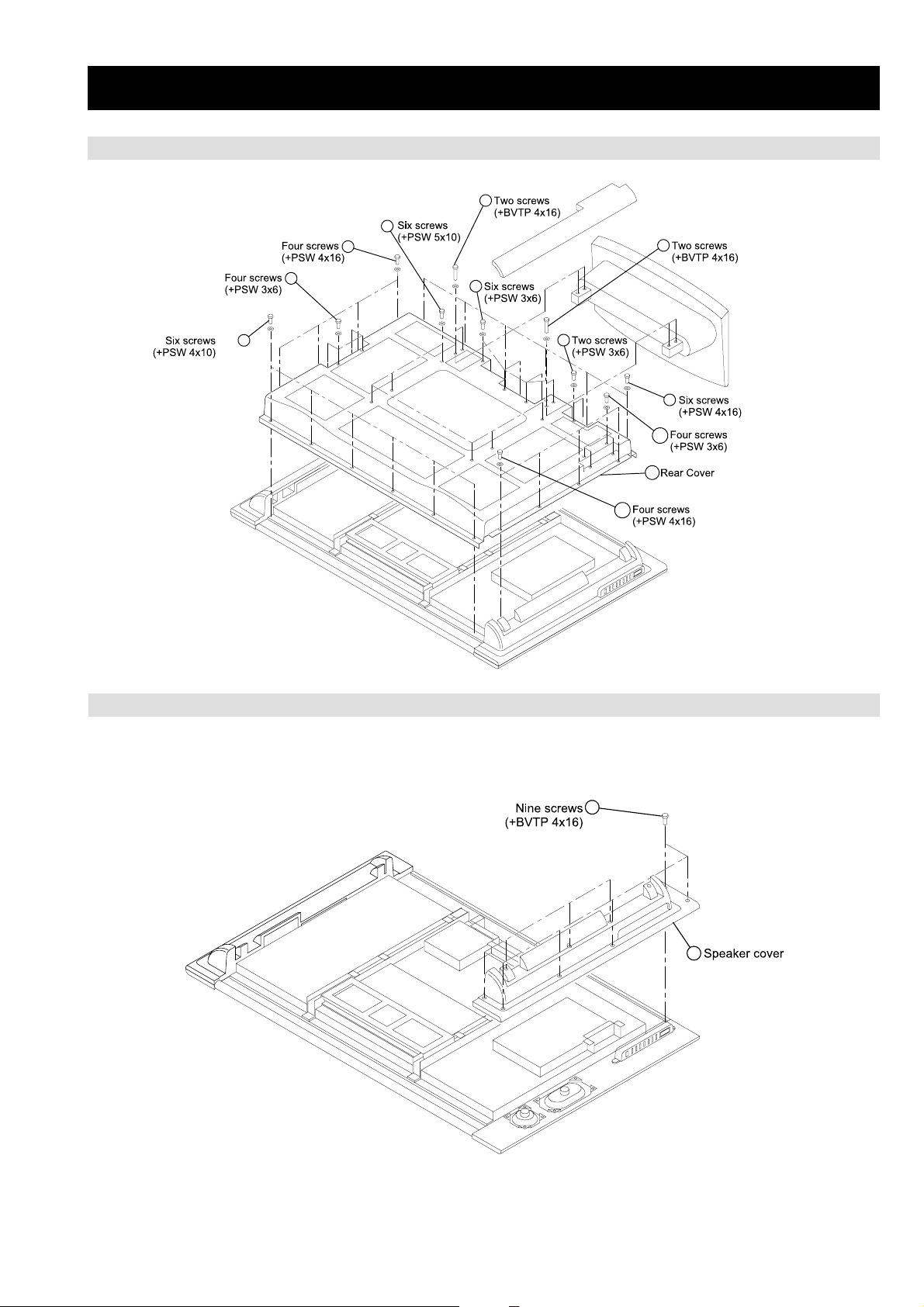
2-1. REAR COVER REMOVAL
SECTION 2 DISASSEMBLY
5
4
3
XS1
RM-Y1011
7
2
1
2-2. SPEAKER COVER REMOVAL
6
8
9
10
11
12
1
2
– 21 –
Page 22
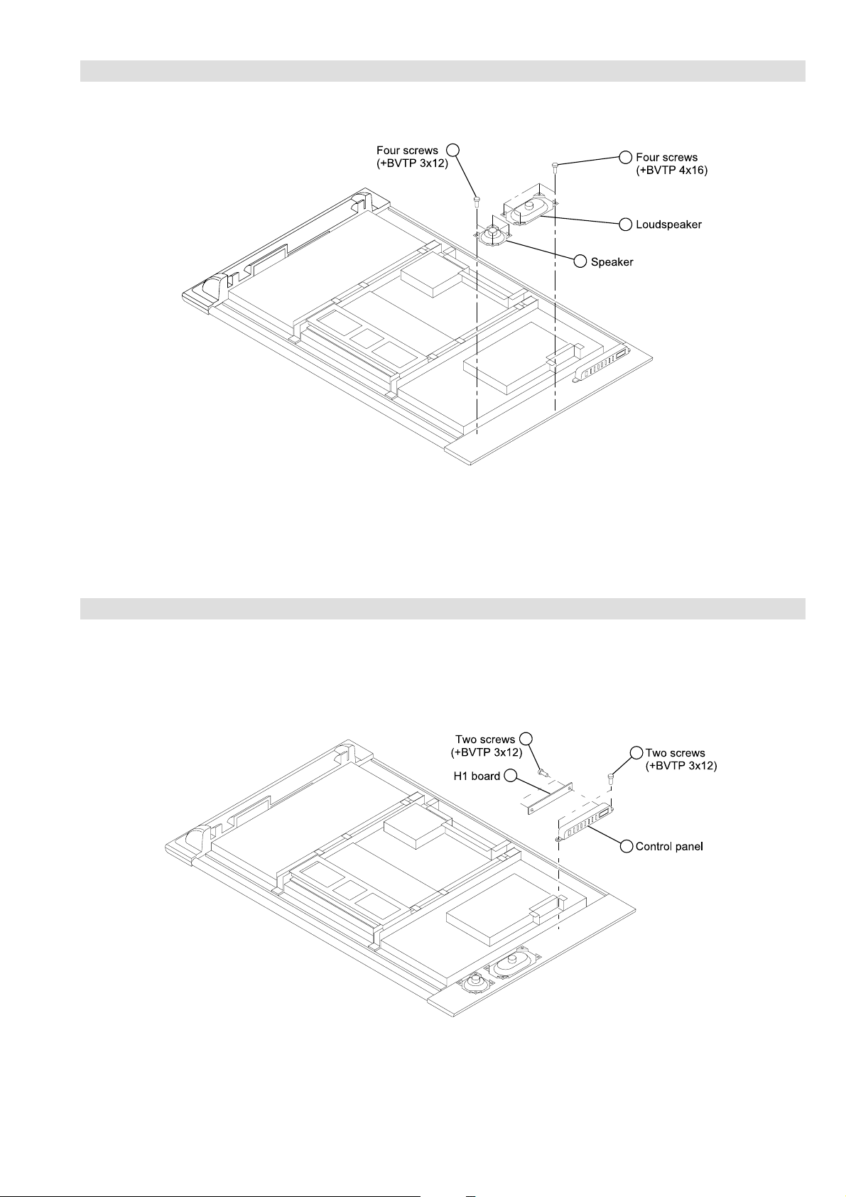
2-3. SPEAKER REMOVAL
XS1
RM-Y1011
1
2
4
3
2-4. H1 BOARD REMOVAL
3
1
4
2
– 22 –
Page 23
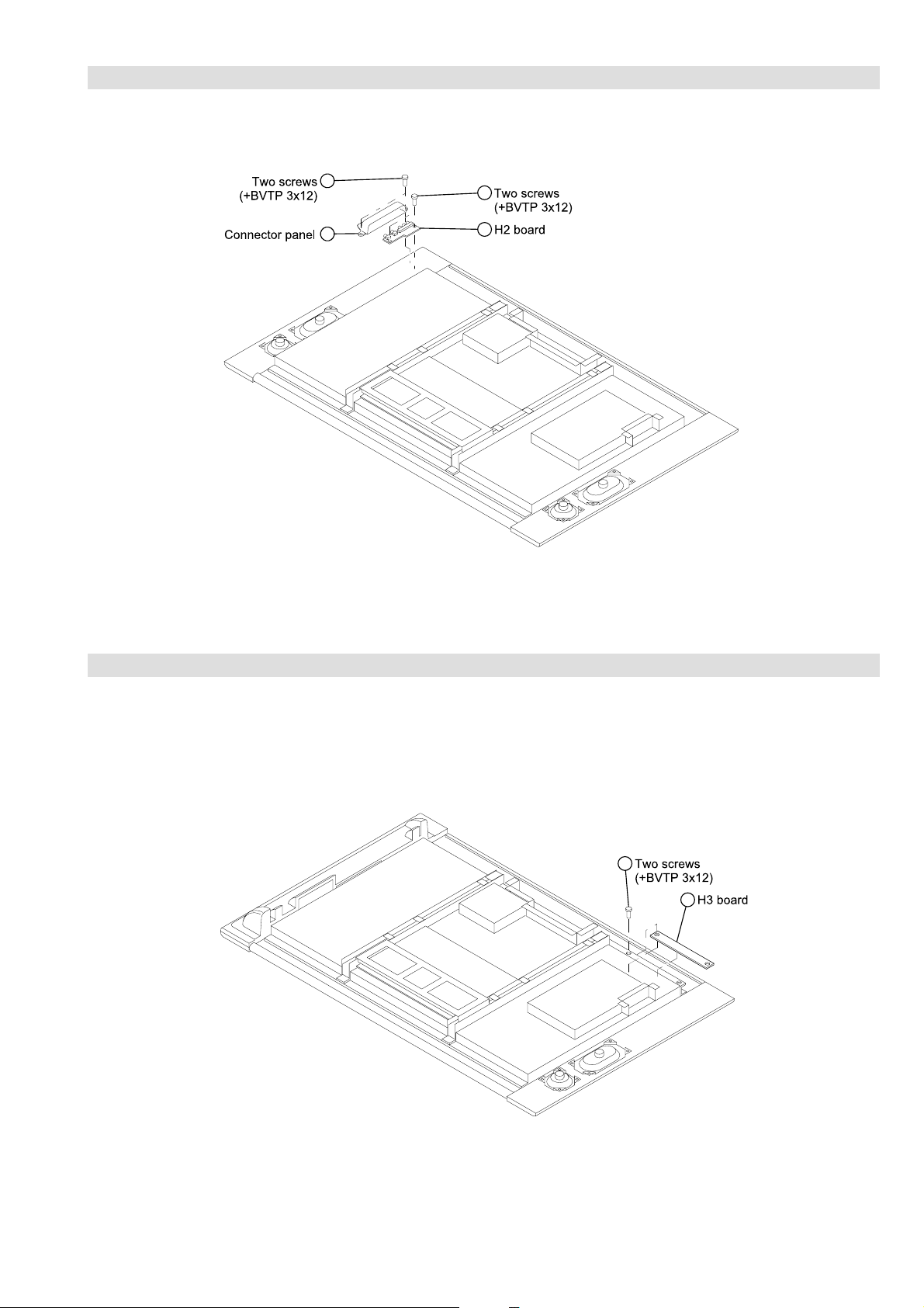
2-5. H2 BOARD REMOVAL
XS1
RM-Y1011
1
2
3
4
2-6. H3 BOARD REMOVAL
1
2
– 23 –
Page 24
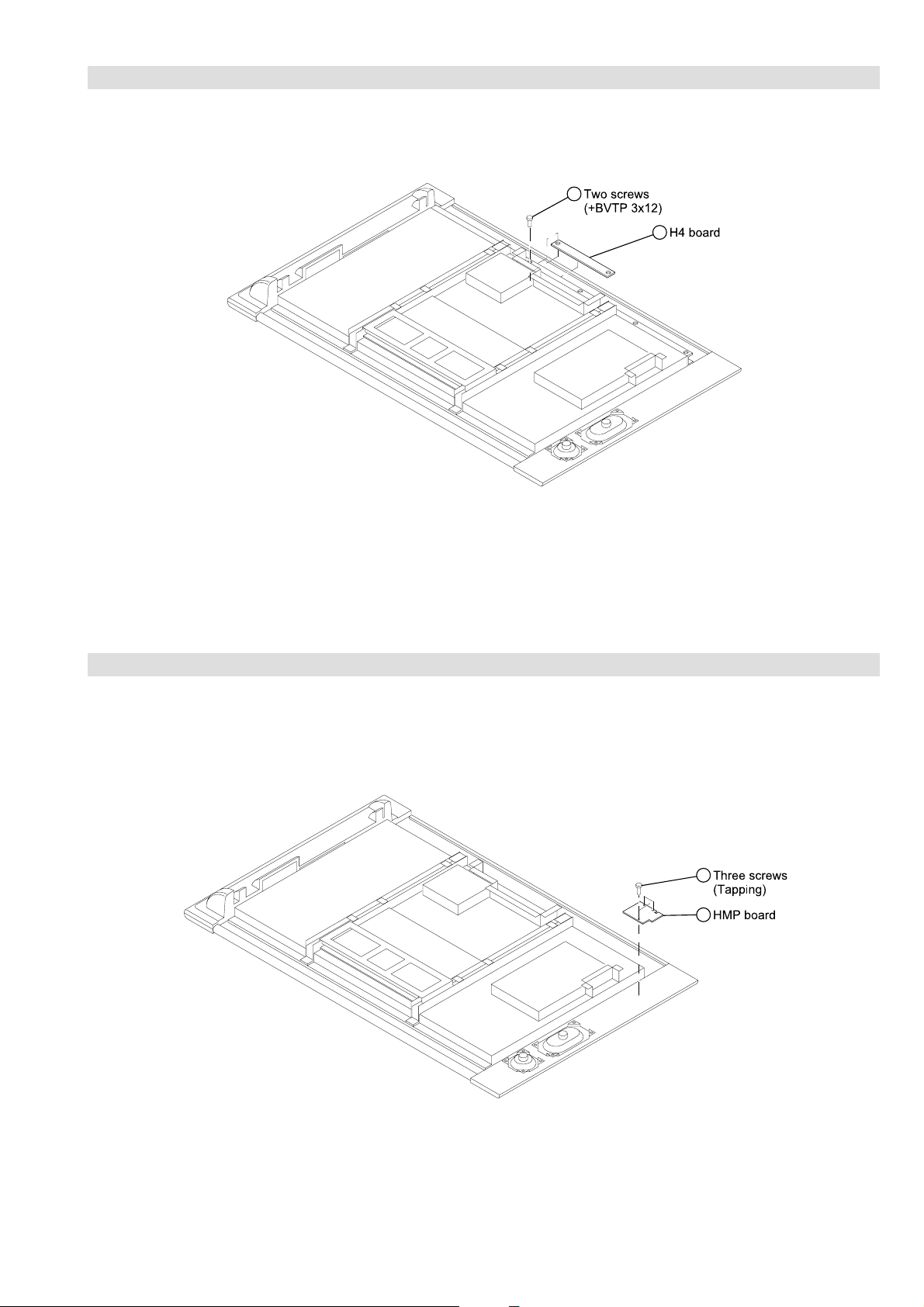
2-7. H4 BOARD REMOVAL
XS1
RM-Y1011
1
2
2-8. HMP BOARD COVER REMOVAL
1
2
– 24 –
Page 25
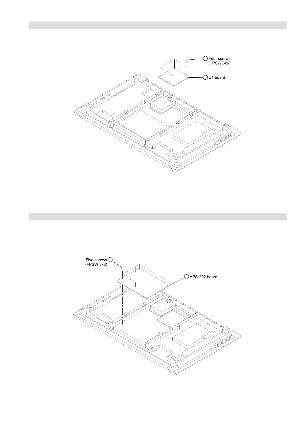
2-9. U1 BOARD REMOVAL
XS1
RM-Y1011
1
2
2-10. APS-202 BOARD REMOVAL
1
2
– 25 –
Page 26
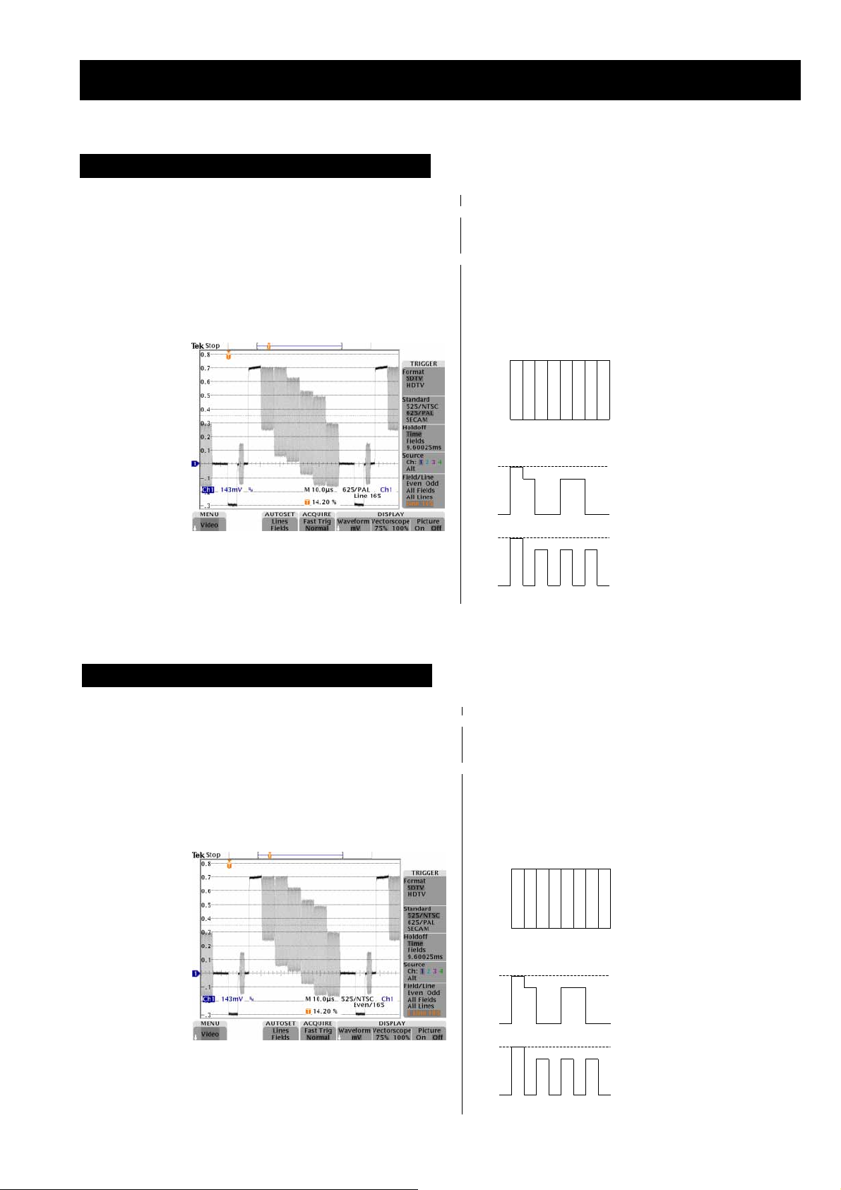
t
)(C)
)(C)
SECTION 3 SET-UP ADJUSTMENTS
t
)(C)
)(C)
3-1. CVBS PAL System Adjustment
CVBS/YC (PAL, SECAM, NTSC), RGB, YUV (15K) System adjustmen
CVBS PAL System adjustment
1) Input CVBS PAL Color Bar signal into AV1 as shown on Figure (1)
EBU Standard Color Bar 100% Luma, 75% Chroma
VG828/ASTRO Pattern No.XXX-OPT 2 No.F
2) Perform automatic adjustment of chroma decoder
3) Check that the detection value of R, G, B is in the standard
shown in the right column.
Figure (1) CVBS PAL EBU Standard Color Bar
White bar RED 216+-3 (A)
White bar BLUE 216+-3 (A)
Black bar RED 16+-3 (D)
Black bar BLUE 16+-3 (D)
Red bar RED
Red bar BLUE 16+-3
Blue bar RED 16+-3 (C)
Blue bar BLUE
75% Color Bar
(A) (B) (C) (D)
ʚ x ʚ x
WhYeCyGMgRBlBk
Cautions The position of (A), (D) excepts
0.700V 2ȑ6
0.525V ȑ62
0.000V 0ȑ6 (one line)
(A) (B
0.700V 2ȑ6
0.525V ȑ62
0.000V 0ȑ6 (one line)
(A) (B
162+-3 (B)
(B)
(C)
162+-3
between for ȑ/ȑ6 from an edge.
RED output
(D)
BLUE output
(D)
XS1
RM-Y1011
3-2. CVBS NTSC System Adjustment
CVBS/YC (PAL, SECAM, NTSC), RGB, YUV (15K) System adjustmen
CVBS NTSC System adjustment
1) Input CVBS NTSC Color Bar signal into AV1 as shown on Figure (1)
EBU Standard Color Bar 100% Luma, 75% Chroma
VG828/ASTRO Pattern No.XXX-OPT 2 No.F
2) Perform automatic adjustment of chroma decoder
3) Check that the detection value of R, G, B is in the standard
shown in the right column.
Figure (1) CVBS NTSC EBU Standard Color Bar
White bar RED 216+-3 (A)
White bar BLUE 216+-3 (A)
Black bar RED 16+-3 (D)
Black bar BLUE 16+-3 (D)
Red bar RED
Red bar BLUE 16+-3
Blue bar RED 16+-3 (C)
Blue bar BLUE
75% Color Bar
(A) (B) (C) (D)
ʚ x ʚ x
WhYeCyGMgRBlBk
Cautions The position of (A), (D) excepts
0.700V 2ȑ6
0.525V ȑ62
0.000V 0ȑ6 (one line)
(A) (B
0.700V 2ȑ6
0.525V ȑ62
0.000V 0ȑ6 (one line)
(A) (B
162+-3 (B)
(B)
(C)
162+-3
between for ȑ/ȑ6 from an edge.
RED output
(D)
BLUE output
(D)
– 26 –
Page 27
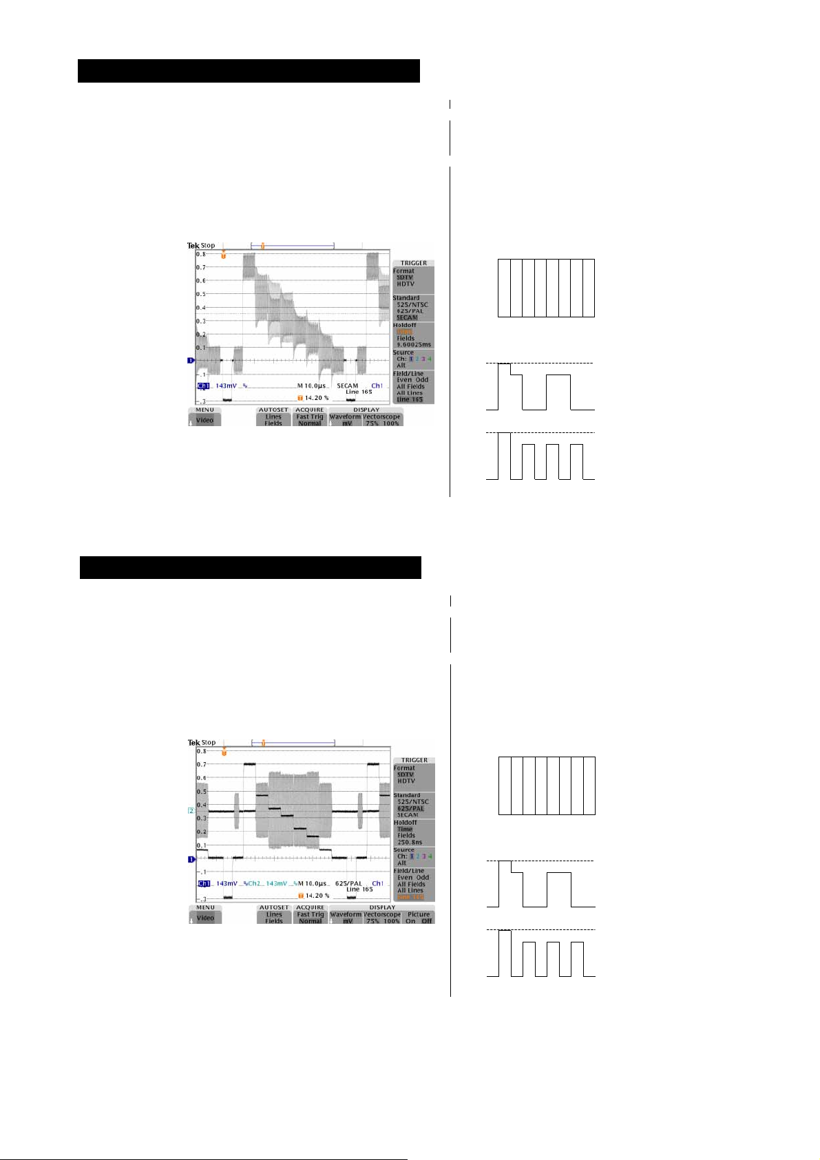
t
)(C)
)(C)
t
)(C)
)(C)
3-3. CVBS SECAM System Adjustment
CVBS/YC (PAL, SECAM, NTSC), RGB, YUV (15K) System adjustmen
CVBS SECAM System adjustment
1) Input CVBS SECAM Color Bar signal into AV1 as shown on Figure (1)
EBU Standard Color Bar 100% Luma, 75% Chroma
VG828/ASTRO Pattern No.XXX-OPT 2 No.F
2) Perform automatic adjustment of chroma decoder
3) Check that the detection value of R, G, B is in the standard
shown in the right column.
Figure (1) CVBS SECAM EBU Standard Color Bar
White bar RED 216+-3 (A)
White bar BLUE 216+-3 (A)
Black bar RED 16+-3 (D)
Black bar BLUE 16+-3 (D)
Red bar RED
Red bar BLUE 16+-3
Blue bar RED 16+-3 (C)
Blue bar BLUE
75% Color Bar
(A) (B) (C) (D)
ʚ x ʚ x
WhYeCyGMgRBlBk
Cautions The position of (A), (D) excepts
0.700V 2ȑ6
0.525V ȑ62
0.000V 0ȑ6 (one line)
(A) (B
0.700V 2ȑ6
0.525V ȑ62
0.000V 0ȑ6 (one line)
(A) (B
162+-3 (B)
(B)
(C)
162+-3
between for ȑ/ȑ6 from an edge.
RED output
(D)
BLUE output
(D)
XS1
RM-Y1011
3-4. YC PAL System Adjustment
CVBS/YC (PAL, SECAM, NTSC), RGB, YUV (15K) System adjustmen
YC PAL System adjustment
1) Input YC PAL Color Bar signal into AV3 as shown on Figure (1)
EBU Standard Color Bar 100% Luma, 75% Chroma
VG828/ASTRO Pattern No.XXX-OPT 2 No.F
2) Perform automatic adjustment of chroma decoder
3) Check that the detection value of R, G, B is in the standard
shown in the right column.
Figure (1) YC PAL EBU Standard Color Bar
White bar RED 216+-3 (A)
White bar BLUE 216+-3 (A)
Black bar RED 16+-3 (D)
Black bar BLUE 16+-3 (D)
Red bar RED
Red bar BLUE 16+-3
Blue bar RED 16+-3 (C)
Blue bar BLUE
75% Color Bar
(A) (B) (C) (D)
ʚ x ʚ x
WhYeCyGMgRBlBk
Cautions The position of (A), (D) excepts
0.700V 2ȑ6
0.525V ȑ62
0.000V 0ȑ6 (one line)
(A) (B
0.700V 2ȑ6
0.525V ȑ62
0.000V 0ȑ6 (one line)
(A) (B
162+-3 (B)
(B)
(C)
162+-3
between for ȑ/ȑ6 from an edge.
RED output
(D)
BLUE output
(D)
– 27 –
Page 28
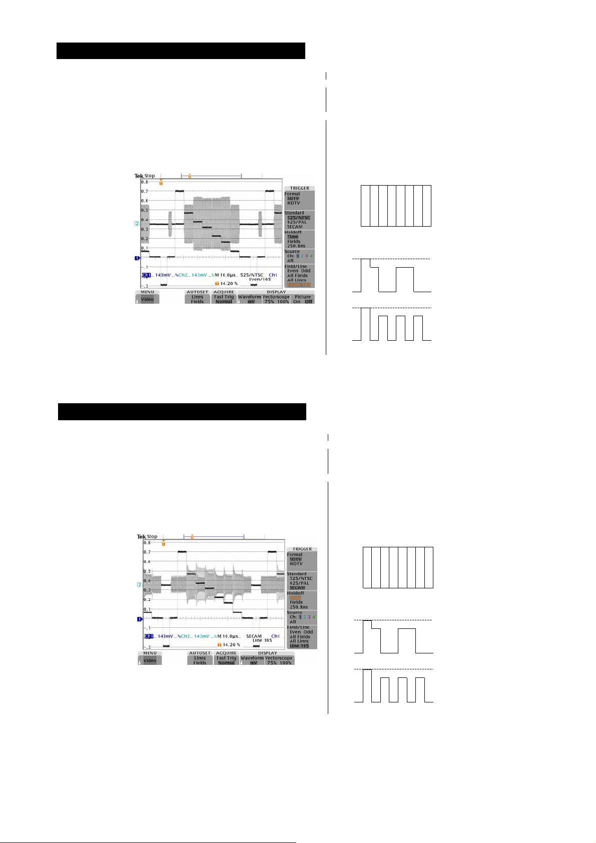
t
)(C)
t
3-5. YC NTSCSystem Adjustment
CVBS/YC (PAL, SECAM, NTSC), RGB, YUV (15K) System adjustmen
YC NTSC System adjustment
1) Input YC NTSC Color Bar signal into AV3 as shown on Figure (1)
EBU Standard Color Bar 100% Luma, 75% Chroma
VG828/ASTRO Pattern No.XXX-OPT 2 No.F
2) Perform automatic adjustment of chroma decoder
3) Check that the detection value of R, G, B is in the standard
shown in the right column.
Figure (1) YC NTSC EBU Standard Color Bar
White bar RED 216+-3 (A)
White bar BLUE 216+-3 (A)
Black bar RED 16+-3 (D)
Black bar BLUE 16+-3 (D)
Red bar RED
Red bar BLUE 16+-3
Blue bar RED 16+-3 (C)
Blue bar BLUE
75% Color Bar
(A) (B) (C) (D)
ʚ x ʚ x
Wh Ye Cy G Mg R Bl Bk
Cautions The position of (A), (D) excepts
0.700V 2ȑ6
0.525V ȑ62
0.000V 0ȑ6 (one line)
(A) (B)(C)(D)
0.700V 2ȑ6
0.525V ȑ62
0.000V 0ȑ6 (one line)
(A) (B)(C)(D)
162+-3 (B)
(B)
(C)
162+-3
between for ȑ/ȑ6 from an edge.
RED output
BLUE output
XS1
RM-Y1011
3-6. YC SECAM System Adjustment
CVBS/YC (PAL, SECAM, NTSC), RGB, YUV (15K) System adjustmen
YC SECAM System adjustment
1) Input YC SECAM Color Bar signal into AV3 as shown on Figure (1)
EBU Standard Color Bar 100% Luma, 75% Chroma
VG828/ASTRO Pattern No.XXX-OPT 2 No.F
2) Perform automatic adjustment of chroma decoder
3) Check that the detection value of R, G, B is in the standard
shown in the right column.
Figure (1) YC SECAM EBU Standard Color Bar
White bar RED 216+-3 (A)
White bar BLUE 216+-3 (A)
Black bar RED 16+-3 (D)
Black bar BLUE 16+-3 (D)
Red bar RED
Red bar BLUE 16+-3
Blue bar RED 16+-3 (C)
Blue bar BLUE
75% Color Bar
(A) (B) (C) (D)
ʚ x ʚ x
Wh Ye Cy G Mg R Bl Bk
Cautions The position of (A), (D) excepts
0.700V 2ȑ6
0.525V ȑ62
0.000V 0ȑ6 (one line)
(A) (B
0.700V 2ȑ6
0.525V ȑ62
0.000V 0ȑ6 (one line)
(A) (B)(C)(D)
162+-3 (B)
(B)
(C)
162+-3
between for ȑ/ȑ6 from an edge.
RED output
(D)
BLUE output
– 28 –
Page 29
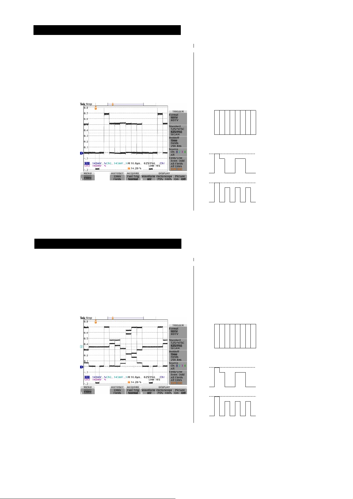
t
)(C)
)(C)
t
)(C)
)(C)
3-7. RGB System Adjustment
CVBS/YC (PAL, SECAM, NTSC), RGB, YUV (15K) System adjustmen
RGB System adjustment
1) Input RGB Color Bar signal into AV1 as shown on Figure (1)
EBU Standard Color Bar 100% Luma, 75% Chroma
VG828/ASTRO Pattern No.XXX-OPT 2 No.F
2) Perform automatic adjustment of chroma decoder
3) Check that the detection value of R, G, B is in the standard
shown in the right column.
Figure (1) RGB EBU Standard Color Bar
White bar RED 216+-3 (A)
White bar BLUE 216+-3 (A)
Black bar RED 16+-3 (D)
Black bar BLUE 16+-3 (D)
Red bar RED
Red bar BLUE 16+-3
Blue bar RED 16+-3 (C)
Blue bar BLUE
75% Color Bar
(A) (B) (C) (D)
ʚ x ʚ x
Wh Ye Cy G Mg R Bl Bk
Cautions The position of (A), (D) excepts
0.700V 2ȑ6
0.525V ȑ62
0.000V 0ȑ6 (one line)
(A) (B
0.700V 2ȑ6
0.525V ȑ62
0.000V 0ȑ6 (one line)
(A) (B
162+-3 (B)
(B)
(C)
162+-3
between for ȑ/ȑ6 from an edge.
RED output
(D)
BLUE output
(D)
XS1
RM-Y1011
3-8. YUV System Adjustment
CVBS/YC (PAL, SECAM, NTSC), RGB, YUV (15K) System adjustmen
YUV (15K) System adjustment
1) Input YUV Color Bar signal into AV4 as shown on Figure (1)
EBU Standard Color Bar 100% Luma, 75% Chroma
VG828/ASTRO Pattern No.XXX-OPT 2 No.F
2) Perform automatic adjustment of chroma decoder
3) Check that the detection value of R, G, B is in the standard
shown in the right column.
Figure (1) YUV EBU Standard Color Bar
White bar RED 216+-3 (A)
White bar BLUE 216+-3 (A)
Black bar RED 16+-3 (D)
Black bar BLUE 16+-3 (D)
Red bar RED
Red bar BLUE 16+-3
Blue bar RED 16+-3 (C)
Blue bar BLUE
75% Color Bar
(A) (B) (C) (D)
ʚ x ʚ x
Wh Ye Cy G Mg R Bl Bk
Cautions The position of (A), (D) excepts
0.700V 2ȑ6
0.525V ȑ62
0.000V 0ȑ6 (one line)
(A) (B
0.700V 2ȑ6
0.525V ȑ62
0.000V 0ȑ6 (one line)
(A) (B
162+-3 (B)
(B)
(C)
162+-3
between for ȑ/ȑ6 from an edge.
RED output
(D)
BLUE output
(D)
– 29 –
Page 30
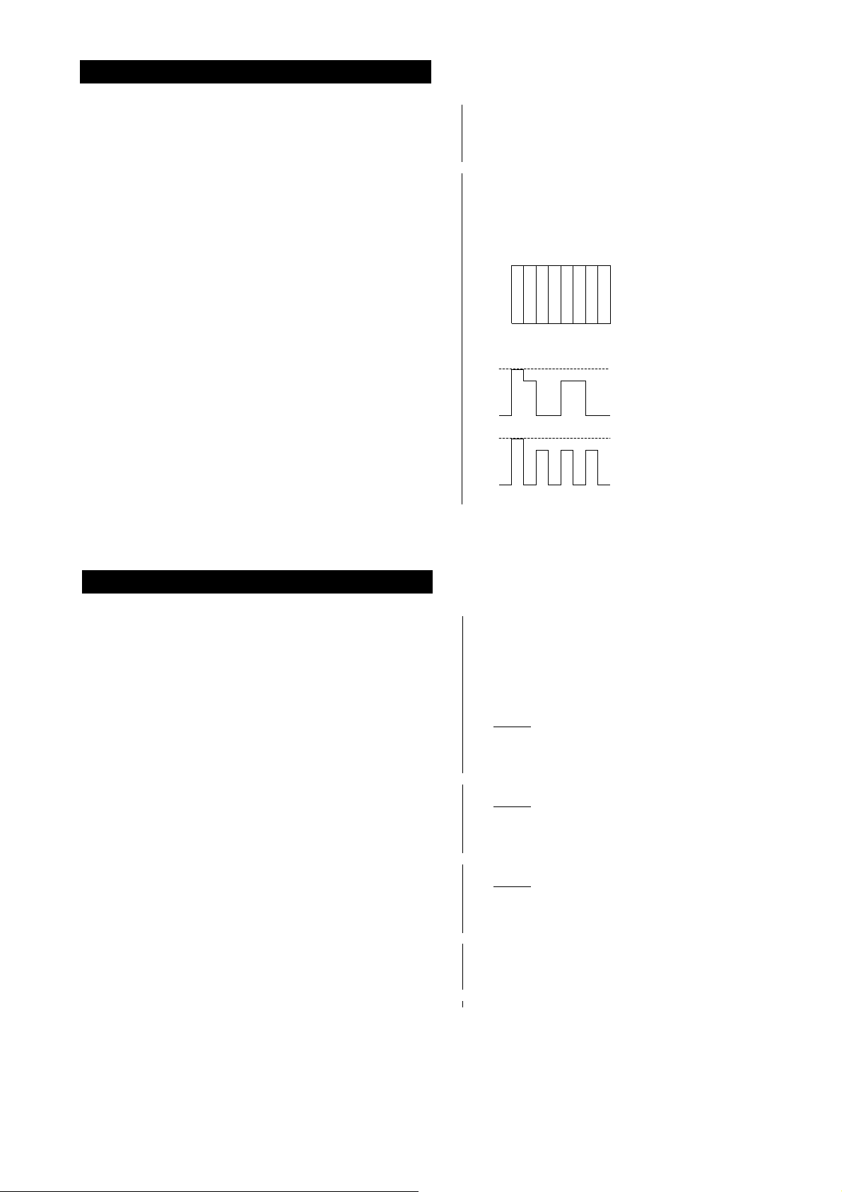
t
3-9. HDTV Component System Adjustment
p
.
)
s
j
D
j
D
/
j
l
/
HDTV COMPONENT 1080i/60Hz System adjustmen
1) Input 1080i/60Hz Color Bar signal into AV4 as shown on Figure (1)
Color Bar 100% Luma, 75% Chroma
VG828/ASTRO Pattern No.955-OPT 2 No.F
2) Perform automatic adjustment of A/D converter
3) Check that the detection value of R, G, B is in the standard
shown in the right column.
Figure (1) 1080i/60Hz Color Bar 100% Luma, 75% Chroma
White bar RED 216+-3 (A)
White bar BLUE 216+-3 (A)
Black bar RED 16+-3 (D)
Black bar BLUE 16+-3 (D)
Red bar RED
Red bar BLUE 16+-3
Blue bar RED 16+-3 (C)
Blue bar BLUE
75% Color Bar
(A) (B) (C) (D)
ʚ x ʚ x
Wh Ye Cy G Mg R Bl Bk
Cautions The position of (A), (D) excepts
0.700V 2ȑ6
0.525V ȑ62
0.000V 0ȑ6 (one line)
(A) (B)(C)(D)
0.700V 2ȑ6
0.525V ȑ62
0.000V 0ȑ6 (one line)
(A) (B)(C)(D)
162+-3 (B)
(B)
(C)
162+-3
between for ȑ/ȑ6 from an edge.
RED output
BLUE output
XS1
RM-Y1011
3-10. White Balance Adjustment
Adjustment of W/B (With internal white signal)
1) Turn on the main
2) Execute the MID_H8_ServiceControl.xl
3) H8_INIT/SVC_FLAG/RGBD=3.
4) Ad
ust W/B of warm
Color tone set to warm (X=0.2943+-0.003)
H8_INIT/SVC_WB/RRTO/warm/ set to FF (Y=0.2840+-0.003)
#1 H8_INIT/SVC_WB/GRTO/warm/
#1 H8_INIT/SVC_WB/BRTO/warm/
#2 Sevice command Direct Select/Service data write(to NVM) -> Send
ust W/B of normal
5) Ad
Color tone set to normal (X=0.2776+-0.003)
H8_INIT/SVC_WB/RRTO/normal/ set to FF (Y=0.2715+-0.003)
#1 H8_INIT/SVC_WB/GRTO/normal
#1 H8_INIT/SVC_WB/BRTO/normal/
#2 Sevice command Direct Select/Service data write(to NVM) -> Send
6) Ad
ust W/B of cool
Color tone set to coo
H8_INIT/SVC_WB/RRTO/cool/ set to FF (Y=0.2718±0.003)
#1 H8_INIT/SVC_WB/GRTO/cool
#1 H8_INIT/SVC_WB/BRTO/cool/
#2 Sevice command Direct Select/Service data write(to NVM) -> Send
ower of XS1
Tool, Measuring, Instrument, Component:
CS-1000 (Minolta
Standard
8400k-27MPC
Standard
11300k-18MPC
Standard
13500k+0MPCD
(X=0.2672±0.003)
When BRTO is set to FF and cannot adjust, it adjusts in RRTO.
Notes)
– 30 –
Page 31
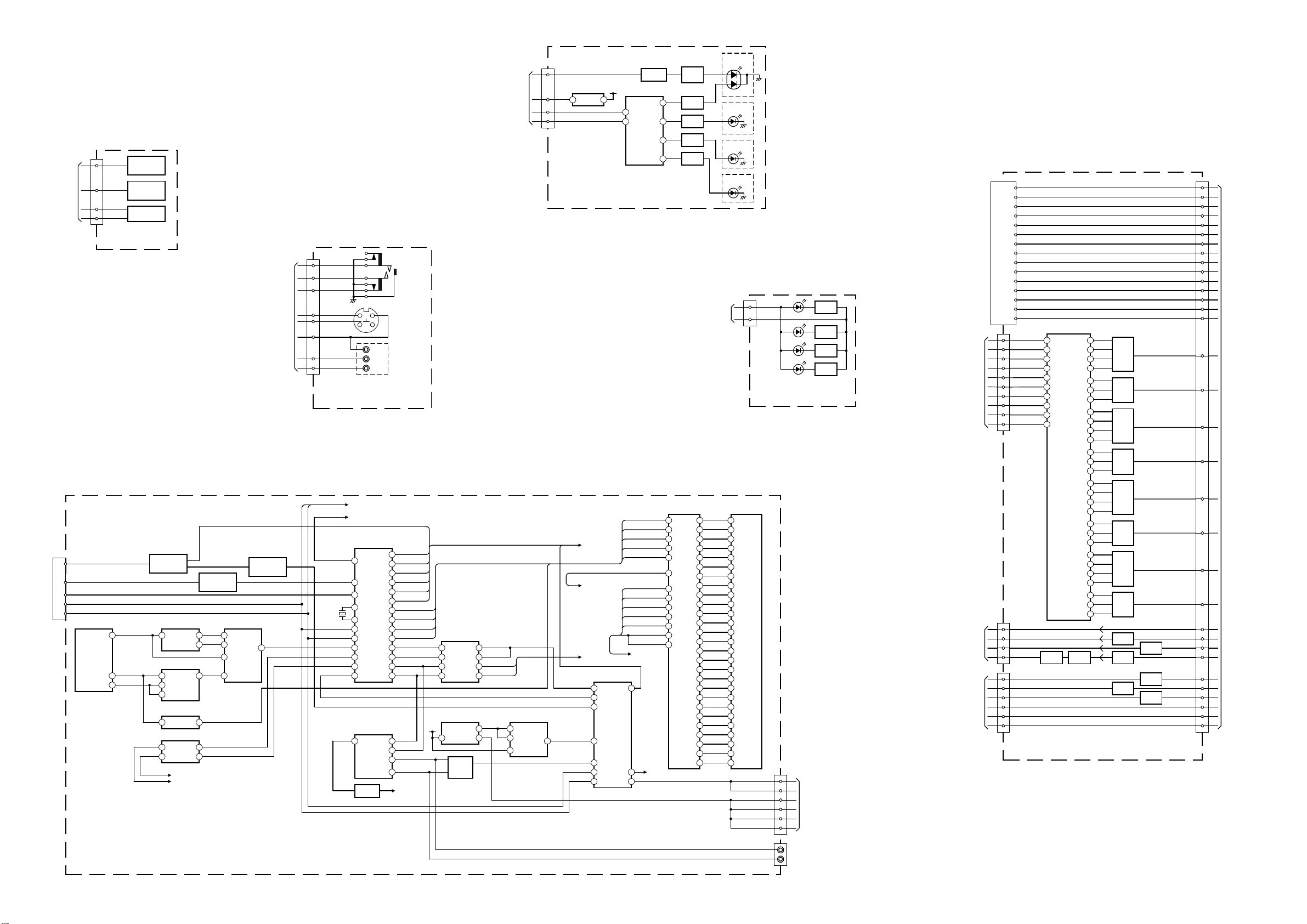
4-1. BLOCK DIA GRAMS (1)
CN9501
5
TO A3 BOARD
CN4603
7
4
3
H1 ( )
TU6000
VIDEO
QSS
FM/AM
SDA
SCL
IC6000
PLL MSP TO AKM
U1 1/2 ( )
SWITCH
KEY 1
S9504, S9505,
S9507, S9508
SWITCH
KEY 2
S9501, S9502,
S9503
P-ON
SWITCH
P-SW(-)
S9506
SWITCH
BUFFER AMP
Q6067, Q6068,
Q6069
IC6018
FIN A
4
VCO OUT
3 16
FIN B
5
2 I/P AND GATE
4
10
5
11
CLK LEVEL SHIFTER
2
HP-DR
1
HP-DL
3
INPUT TERMINAL,
AV SW, AUDIO
IC6017
8 DIVIDER
IC6010
IC6800
TO (J)
SHEET 2
BUFFER AMP
Q6002, Q6003,
Q6064
2
VDD
AKM CLK
4
HP-MSP-R
7
HP-MSP-L
6
POWER/EPG
G
R
TO A3 BOARD
CN4901
107
106
105
104
103
102
101
100
NOE
A16
A15
A14
A13
A12
A11
A10
A9
A8
A7
A6
A5
A4
A3
A2
A1
A0
NWE
STBY
D9701
RED/GREEN
PIC OFF
D9704
BLUE
TIMER
D9703
STBY
D9702
CN9801
IC6013
IM SRAM
21
20
19
18
17
15
14
13
24
2
31
3
28
4
25
23
26
27
5
6
7
8
9
10
11
12
29
1
2
FAN 1 ERR
FAN 2 ERR
FAN 1 DRIVE
FAN 2 DRIVE
FAN 3 DRIVE
FAN 4 DRIVE
D9801
+5V
LOGO
D9802
D9803
D9804
CN6004
1
LED
H4 ( )
4
2
TO FAN S
5
8
11
Q9801
Q9802
Q9803
Q9804
TO A4 BOARD
CN4103
TO U1 BOARD
CN6011
TO A4 BOARD
CN4104
TU7000
CN7002
CN7001
CN7000
PRESET
SDA
SCL
PD0/(PD
SERIAL)
PD1
PD2
PD3
PD4
PD5
PD6
PD7
PD0 CLK
PD0 VAL
PD0ERR/
(RSLOCK)
PDSYNC
14
LV_A-
13
LV_A+
11
LV_B-
10
LV_B+
8
LV_C-
7
LV_C+
5
LV_CLK-
4
LV_CLK+
2
LV_D-
1
LV_D+
9
RESET_N
7
R_N
5
L_N
1
CVBS-N
1
Y_N_BKP
3
CR_N_BKP
5
CB_N_BKP
7
FBLK_N_BKP
9
DPI_SDA
11
DPI_SCL
N1 ( )
IC7000
LVDS TRANSMITTER
31 33
30
29
28
25
24
23
22
21
20
TA0
TA1
TA2
TA3
TA4
TA5
TA6
TB0
TB1
TB2
TB3
TB4
TB5
TB6
TC0
TC1
TC2
TC3
TC4
TC5
TC6
TD0
TD1
TD2
TD3
TD4
TD5
TD6
FILTER
BUFFER
FL7000
Q7001
DIGITAL TUNER
CN7004
A8
FE-RESET
B7
SDA_N
A7
SCL_N
A1
IN_TS(0)
B1
IN_TS(1)
A2
IN_TS(2)
B2
IN_TS(3)
A3
IN_TS(4)
B3
IN_TS(5)
A4
IN_TS(6)
B4
IN_TS(7)
A5
IN_TSCLK
A9
IN_TSEN
B8
RS LOCK
VDO(0)
VDO(1)
VDO(2)
VDO(3)
VDO(4)
VDO(5)
VDO(6)
VDO(7)
RIGHT
LEFT
YUV_V
FAST BLK
SDA_TV
SCL_TV
B5
B24
C24
B23
TO N BOARD
C23
B22
C22
B21
C21
C7
A32
B32
A29
A26
A28
A27
A30
B11
A11
IN_TSPSYNC
34
RB7000
35
36
37
38
RB7001
40
41
42
RB7002
44
45
46
48
RB7003
49
50
52
RB7004
53
54
55
57
RB7005
58
59
61
RB7006
62
63
64
1
RB7007
3
NOT N RESET
BUFFER
Q7000
BUFFER
Q7002
BUFFER
Q7006
BUFFER
Q7003
CVBS_OUT
YUV_Y/YC_Y
YUV_U/YC_C
BUFFER
Q7005
BUFFER
Q7004
TO U1 BOARD
CN6003
CN9601
CN9701
8
TO A3 BOARD
CN4601
3
5
6
POWER LED
IR
SDA
SCL
IC9701
SIRCS
+5V
VCCOUT
IC9702
4 CH ADDRESS
14
15
SWITCH
Q9705
DAC 4
DAC 3
DAC 2
DAC 0
LED & IR
H3 ( )
HP R
13
HP L
11
HP SW
15
3
C
5
PORT
1
Y/CVBS
7
L FR ONT
9
R FRONT
4 3
2 1
J9601
Y/C
VIDEO
L
R
J9600
HEADPHONE
RECEIVER
LED
DRIVER
Q9703
SWITCH
3
Q9704
Q9700
4
SWITCH
Q9701
5
SWITCH
Q9702
7
SWITCH
J9602
INPUT
SW-MSP-OUT
IF IN 1
MONO IN
X6007
SDA
SCL
SC3-OUT-R
SC3-OUT-L
RESET MSP
MUTE
TERMINAL
TO (A)
SHEET 2
TO (H)
SHEET 2
IC6027
MULTI-STANDARD
SOUND PROCESSOR
30
67
60
71
72
3
2
74
24
25
21
IC6003
L/R AMP
6
SWITCH
Q6014
R MAIN
57
L MAIN
56
MS-L
53
MS-R
54
TV-L
37
TV-R
36
12-MSP-CL
4
12-MSP-WS
5
12-MSP-OUT
6
12-MSP-IN
7
SC2-OUT L
34
SC2-OUT R
33
SP-OUT L
28
SP-OUT R
27
SP R
18
SP L
10
OUT 1
3
OUT 2
23
TO (F)
SHEET 2
14V
IC6030
OP AMP
3
15
7
IC6016
VOLTAGE REG
SP PROT
Q6015
Q6016
Q6017
IC6012
AUDIO DELAY DSP
12-MSP CL
18
12-MSP WS
TO (B)
SHEET 2
12-MSP OUT
12-MSP IN
AKM-CLK
SYS-RST
TO (C)
SHEET 2
RQ
SCLK
SI-DSP
SO-DSP
DSP-RDY
RESET-DSP
FIX VAR
2
16
LINE L5
5
LINE R5
1311
IC6001
OP AMP
3
2
4
31
5
1
RESET MSP
COINCIDENCE
FAN CONTROL
SP PROT
TO (D)
SHEET 2
PORT EXPANDER
5 1
6
2
4
10
SCL
15
SDA
IC6031
TO (E)
SHEET 2
7
914
TO (G)
SHEET 2
68
17
67
15
66
13
65
24
64
63
2
62
61
29
60
30
59
31
58
32
57
33
56
3
55
4
54
53
52
51
48
47
46
45
44
43
42
41
40
H2( )
AMPLIFIER/
SWITCH
Q6070, Q6071
IC6002
DIVIDER
51
9
11
16
AUDIO CLOCK
10
CN6000
TO SPEAKERS
- 31 -
Page 32
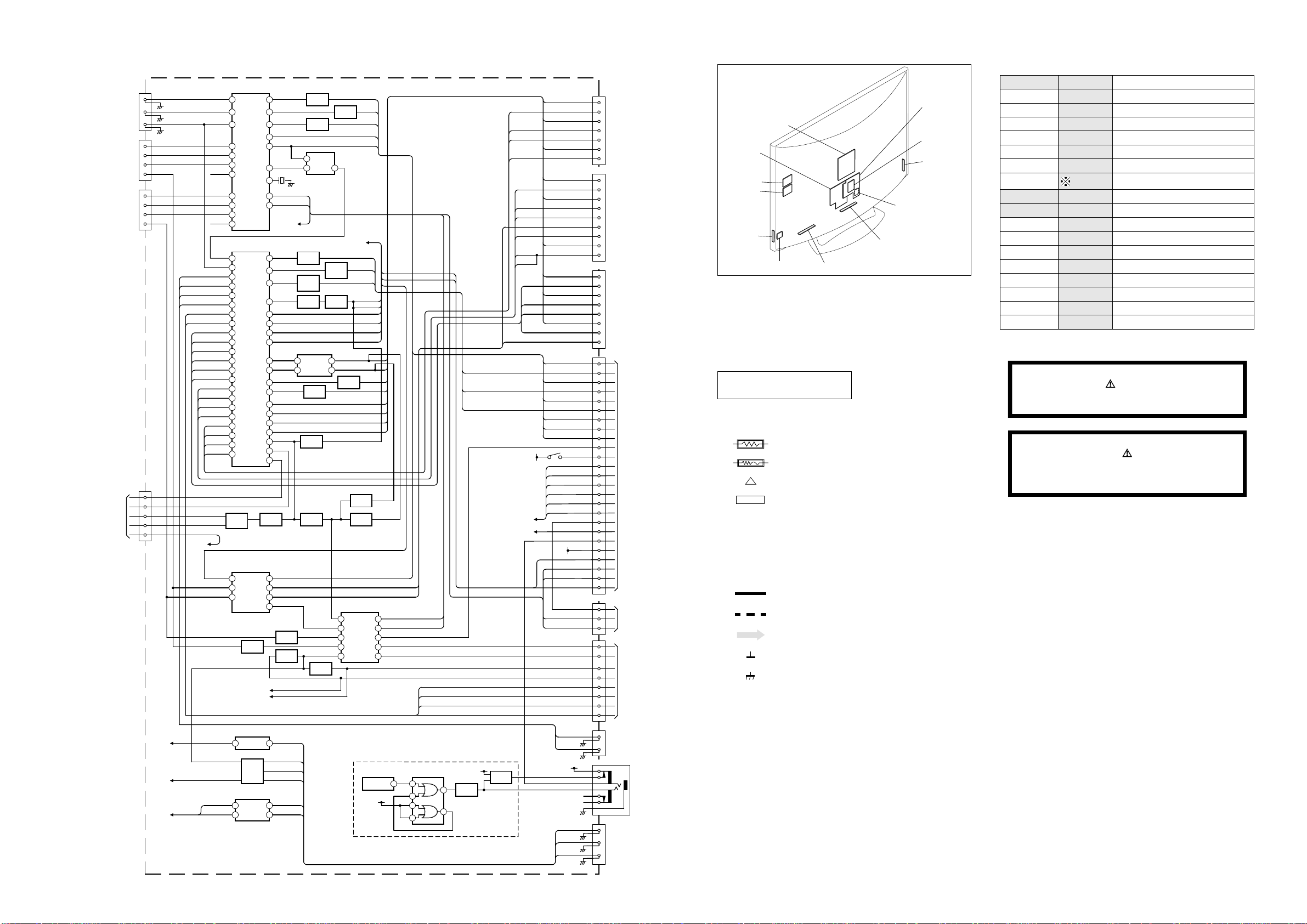
4-2. CIRCUIT BOARD LOCATION
4-3. SCHEMATIC DIAGRAMS AND
PRINTED WIRING BOARDS
Note :
• All capacitors are in µF unless otherwise noted.
• pF : µµF 50WV or less are not indicated except for
electrolytic types.
• Indication of resistance, which does not have one for
rating electrical power, is as follows.
Pitch : 5mm
Electrical power rating : 1/4W
• Chip resistors are 1/10W
• All resistors are in ohms.
k = 1000 ohms, M = 1000,000 ohms
• : nonflammable resistor.
• : fusible resistor.
• : internal component.
• : panel designation or adjustment for repair.
• All variable and adjustable resistors have
characteristic curve B, unless otherwise noted.
• All voltages are in Volts.
• Readings are taken with a 10Mohm digital mutimeter.
• Readings are taken with a color bar input signal.
• Voltage variations may be noted due to normal production
tolerences.
•: B + bus.
• : B - bus.
• : RF signal path.
• : earth - ground.
• : earth - chassis.
Reference Information
RESISTOR RN
: METAL FILM
RC
: SOLID
FPRD
: NON FLAMMABLE CARBON
FUSE
: NON FLAMMABLE FUSIBLE
RS
: NON FLAMMABLE METAL OXIDE
RB
: NON FLAMMABLE CEMENT
RW
: NON FLAMMABLE WIREWOUND
: ADJUSTMENT RESISTOR
COIL LF-8L
: MICRO INDUCTO R
CAPACITOR TA
: TANTALUM
PS
: STYROL
PP
: POLYPROPYLENE
PT
: MYLAR
MPS
: METALIZED POLYESTER
MPP
: METALIZED POLYPR OPYLENE
ALB
: BIPOLAR
ALT
: HIGH TEMPERATURE
ALR
: HIGH RIPPLE
Les composants identifiés par une trame et
par une marque sont d'une importance
critique pour la sécurité. Ne les remplacer
que par des pièces de numéro spécifié.
specified.
Note :
The components identified by shading
and marked are critical for safety.
Replace only with the part numbers
specified in the parts list.
Note :
CVM Board
A Board
S1 Board
VM
C
H
D1
A
J
A2
N
D
A1
D2
C
A
U1
H1
H2
H3
APS202
MS2A
A3
A4
H4
HMP
N
N1
4-1. BLOCK DIA GRAMS (2)
J6006
R
J6001 1/2
15
J6003 1/2
RED
7
BLUE
11
GREEN
16
BLK1
15
RED
BLUE
GREEN
BLK2
7
11
16
TO N1 BOARD
CN7001
CN6011
7
5
2
1
9
TO (H)
SHEET 1
R_N
L_N
CVBS_N-
CVBS_N+
RESET_N
TO (G)
SHEET 1
TO (F)
SHEET 1
LINE R/R5
TO (D)
SHEET 1
U1 2/2 ( )
YUV CR
YUV CB
YUV Y
R1
B1
G1
CVBS 2
R2
B2
G2
CVBS 1
DC OUT
YUV Y
Y CVBS-F
LIN-F
R IN-F
C-F
YUV-L
YUV-R
MODE 3
C IN 3
R IN 3
Y IN 3
L IN 3
V IN 3
MODE 2
R IN 2
L IN 2
V IN 2
MODE 1
R IN 1
L IN 1
V IN 1
AVL SEL
BLK1
BLK2
SW-MSP-OUT
MUTE L1
MUTE AMP
LINE L5
LINE R5
IC6004
YUV SWITCH
41
42
43
7
8
9
4
1
2
3
10
IC6006
AV SWITCH
36
30
22
23
25
26
29
31
20
19
18
17
16
15
13
11
9
8
6
4
2
1
FILTER
FL8000
IC6007
MULTIPLEXER/
DEMULTIPLEXER
11
2
1
AMP
Q6035
SHEET 1
IC6008
3 1
AMP
Q6064
Q6040
Q6039
IC6701
OP AMP
5
3
INPUT TERMINAL,
AV SW, AUDIO
TO (J)
27
26
25
23
22
20
30
31
58
56
53
63
64
62
54
52
59
41
44
45
43
40
38
60
59
61
BUFFER
Q6027
15
13
12
10
SW-OUT
LINE-L
LINE-R
7
1
SEL Y OUT
SEL CB OUT
SEL CR OUT
V SEL
H SEL
CLAMP SW
X6003
SCL
SDA
TO (A)
SHEET 1
C OUT 1
Y OUT 1
V OUT 1
TV-R
TV-L
R-MAIN
L-MAIN
L DIG
R DIG
V OUT 2
V/Y OUT 3
R OUT 3
L OUT 3
R OUT 2
L OUT 2
V6
LV6
RV6
FSW-OUT
AV LINK 3
AV LINK 2
FSW SELECT
AMP
Q6037
SWITCH
Q6073
SW-OUT
LINE L
LINE R
BUFFER
Q6019
Y SEL
CB SEL
CR SEL
BUFFER
Q6020
BUFFER
Q6018
1
4 217
IC6005
EXT CLAMP
TO (B)
SHEET 1
BUFFER
Q6030
BUFFER
Q6022
Q6028
SWITCH
Q6034
5
3 161
IC6700
OP AMP
AMP
Q6023
Q6101
Q6102
C MAIN
BUFFER
Y MAIN
Q6025
Q6043
CVBS MAIN
TUN-MAIN
AMP
Q6036
L TUN
7
R TUN
V OUT 2
AMP
Q6032
V OUT 3
SWITCH
Q6103
SWITCH
Q6100
MUTE_RF_DIG
FSW SCART 2
FSW SCART 1
MUTE L1
SWITCH
Q6074
HP-R
HP-L
SWITCH
Q6104
IC6032
PORT EXPANDER
4
3
2
1
6
AV LINK 2
TO (E)
SHEET 1
TO (C)
SHEET 1
SDA
14
SCL
15
RESET-CD
5
HP-SW
9
YC-PORT
10
BUFFER
Q6038
+3.3V
SWITCH
Q6021
AV MOUSE
IC6015
INVERTER
+3.3V
IC6014
NAND
5
7
3
6
1
7
2
R IN 1
L IN 1
MODE 1
V IN 1
R IN 3
L IN 3
MODE 3
C IN 3
V IN 3
Y IN 3
R IN 2
L IN 2
MODE 2
V IN 2
AV LINK 2
+3.3V
STBY
R-TUN
L-TUN
CVBS-TUN
R OUT 3
L OUT 3
V OUT 3
R OUT 2
V OUT 2
CB SEL
Y SEL
CR SEL
FSW OU T
H SEL
V SEL
S6201
+3.3V
CVBS MAIN
RESET CD
RESET DSP
RESET SYS
Y CVBS-F
YUV-L
YUV-R
+3.3V
SW-OUT
LINE L
LINE R
R OUT
R IN
L OUT
MODE
V OUT
V IN
R OUT
R IN
L OUT
MODE
AVL
C IN
V OUT
Y/V IN
R OUT
R IN
L OUTL OUT 2
L OUT
MODE
V OUT
V IN
AVL
U SEL
Y SEL
Y MAIN
V SEL
C MAIN
FSW SEL
H SEL
V SEL
UP-SW
DSP-RDY
SO-DSP
SI-DSP
SCLK
RS232
SIRCS
MS-L
SDA
SCL
MS-R
SDA
SCL
HP-SW
YC PORT
HP-L
HP-R
L IN-F
R IN-F
J6001 (2/2)
1
2
3
6
L IN
(SCART 1)
8
19
20
J6000
1
2
3
6
L IN
8
(SCART 3)
10
15
19
20
J6003
1
2
3
6
L IN
(SCART 2)
8
19
20
10
CN6002
A1
B1
A3
B3
A5
B5
A7
A9
A11
B12
B13
B15
B16
TO A3 BOARD
B17
B18
B19
RQ
B20
A21
CS
B21
B22
A26
B27
A28
A29
B29
CN6015
4
CS
3
TO A3 BOARD
2
CN6003
15
5
11
13
TO H2 BOARD
1
CN9601
3
C-F
7
9
J6005
J6501
J6004
- 32 -
Page 33
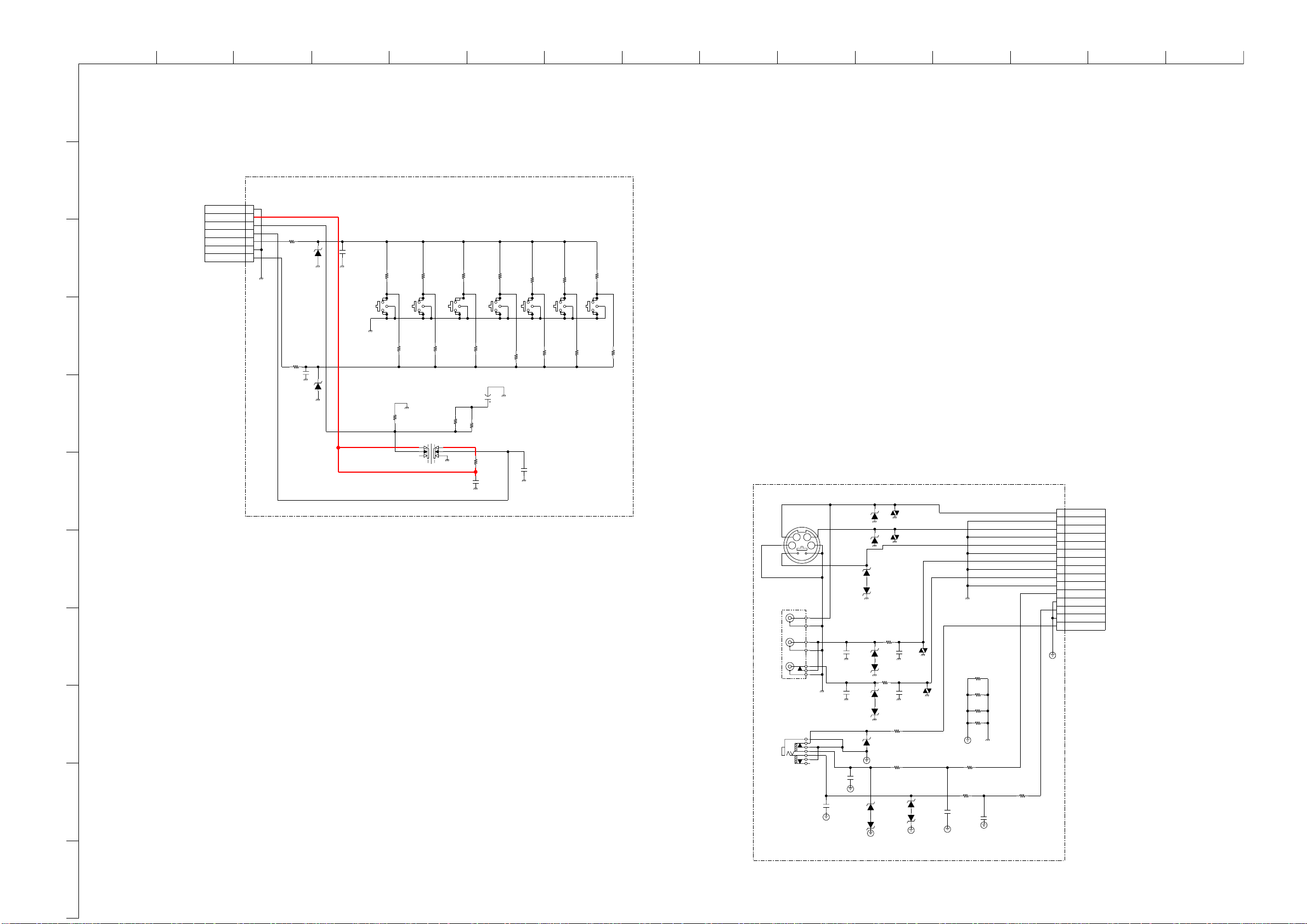
ABCDE F
34
1
2
BLK
4P
J9601
L
R
V
J9602
J9600
UDZS-TE17-12B
D9600
UDZS-TE17-12B
D9601
UDZS-TE17-12B
D9602
UDZS-TE17-12B
D9603
UDZS-TE17-12B
D9604
UDZS-TE17-12B
D9605
UDZS-TE17-12B
D9607
UDZS-TE17-12B
D9606
UDZS-TE17-12B
D9608
UDZS-TE17-12B
D9609
UDZS-TE17-12B
D9610
UDZS-TE17-12B
D9611
UDZS-TE17-12B
D9612
VD9601
XX
1
2
3
4
5
6
7
8
9
10
11
12
13
14
15
BRN
15P
CN9601
Y/CVBS
GND
C
GND
PORT
GND
L_FRONT
GND
R_FRONT
GND
HP_L
GND
HP_R
GND
HP_SW
VD9600
XX
XX
C9600
XX
C9602
VD9603
XX
XX
C9601
XX
C9603
VD9602
XX
C9604
XX
C9606
XX
C9607
XX
C9605
CHIP
0
R9606
100
R9601
1/10W
100
R9600
1/10W
100
R9602
CHIP
0
R9605
JR9601
XX
JR9602
XX
JR9603
XX
JR9604
XX
CHIP
0
R9604
CHIP
0
R9603
H2.-XS1
COMPONENTS MARKED AS XX ARE NOT FITTED TO THIS MODEL
TO U1 BOARD
CN6003
H2
INPUT TERMINAL
G
HI JKLMN
O
1
~ H1 Board Schematic Diagram [ Switch ] ~
CN9501
7P
STBY5V
P-SW(-)
GND
P-ON
KEY1
GND
KEY2
H1.-XS1
1
2
3
4
5
6
7
R9501
100
1/10W
D9501
UDZS-TE17-12B
C9501
0.1
16V
H1
SWITCH
COMPONENTS MARKED AS XX ARE NOT FITTED TO THIS MODEL
R9509
XX
R9516
XX
R9502
XX
R9512
47k
1/10W
R9510
10k
1/10W
R9511
4.7k
1/10W
R9520
0
CHIP
2
TO A3 BOARD
CN4603
3
4
5
6
7
8
9
10
11
C9505
0.1
16V
R9514
100
1/10W
D9502
UDZS-TE17-12B
S9501
S9502
R9513
10k
1/10W
A/D TV CH- CH+ AUTO SELECT VOL- VOL+
R9506
XX
R9515
4.7k
1/10W
R9507
XX
S9506
S9503
C9502
XX
R9503
R9508
XX
0
CHIP
R9505
0
C9504
0.01
50V
S9504
S9505
R9521
XX
C9503
0.01
50V
R9517
XX
S9507
R9518
XX
S9508
R9519
XX
~ H2 Board Schematic Diagram [ Input Terminal ] ~
- 33 -
Page 34
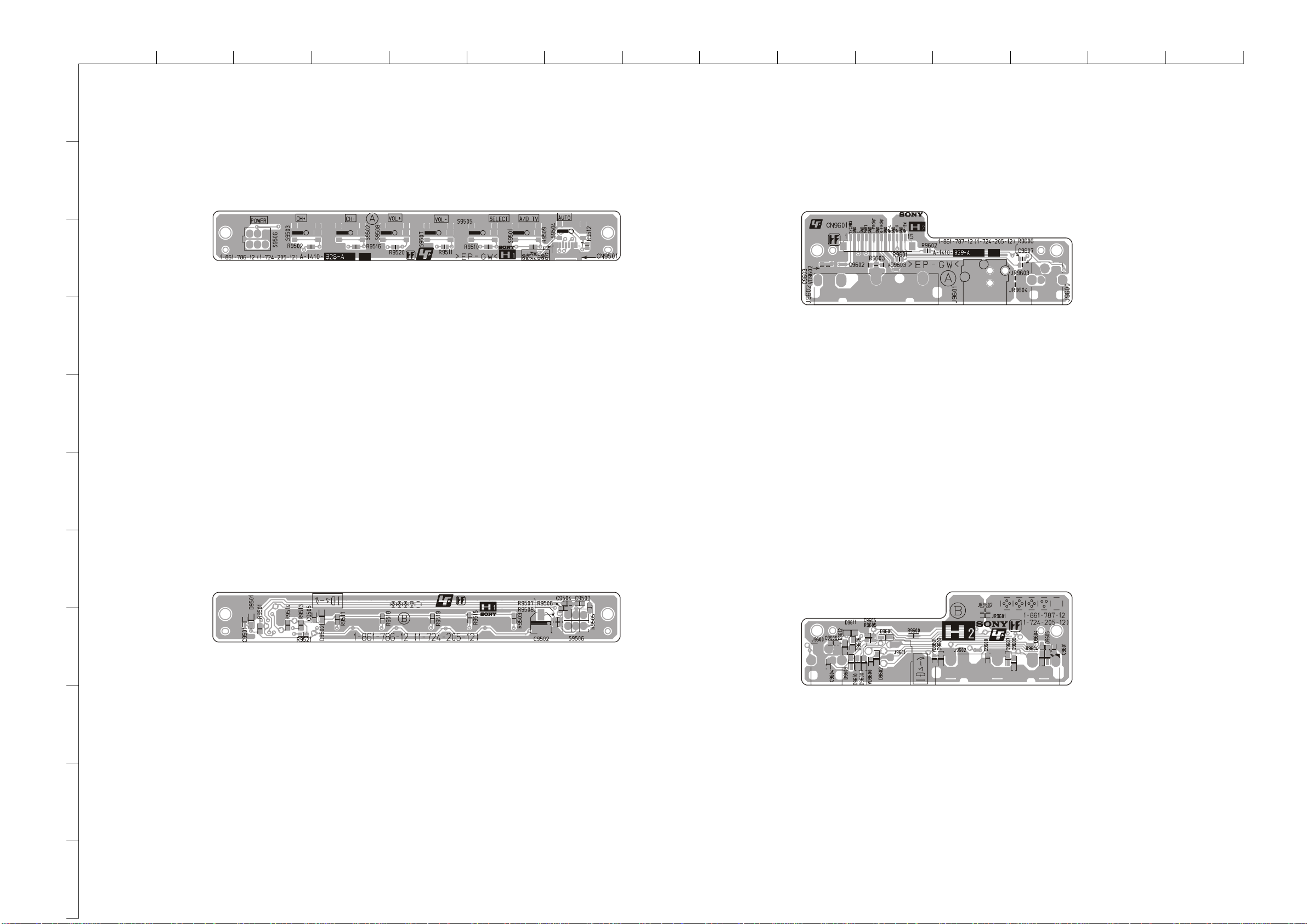
ABCDE F
1
2
G
~ H1 Printed Wiring Board Conductor Side A ~
3
4
HI JKLMN
~ H2 Printed Wiring Board Conductor Side A ~
O
5
6
7
8
9
~ H1 Printed Wiring Board Conductor Side B ~
~ H2 Printed Wiring Board Conductor Side B ~
10
11
- 34 -
Page 35
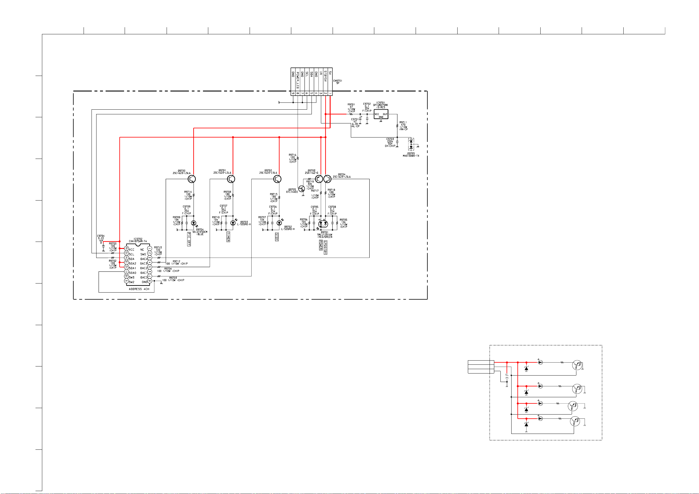
ABCDE F
1
2
3
GRY
3P
CN9801
+5V
LOGO
GND
XX
C9801
NSPW515BSA0
D9801
NSPW515BSA0
D9802
NSPW515BSA0
D9803
NSPW515BSA0
D9804
DTC114EUA-T106
Q9801
DTC114EUA-T106
Q9802
DTC114EUA-T106
Q9803
DTC114EUA-T106
Q9804
R9801
1/10W
100
R9802
1/10W
100
R9803
1/10W
100
R9804
1/10W
100
D9805
XX
D9806
XX
D9807
XX
D9808
XX
H4.-XS1
COMPONENTS MARKED AS XX ARE NOT FITTED TO THIS MODEL
H4
LED
TO A3 BOARD
CN4901
G
HI JKLMN
O
1
TO A3 BOARD
CN4601
H3.-XS1
2
3
4
470
5
6
7
~ H3 Board Schematic Diagram [ LED & IR Receiver ] ~
8
9
10
11
H3
LED & IR RECEIVER
COMPONENTS MARKED AS XX ARE NOT FITTED TO THIS MODEL
- 35 -
~ H4 Board Schematic Diagram [ LED ] ~
Page 36
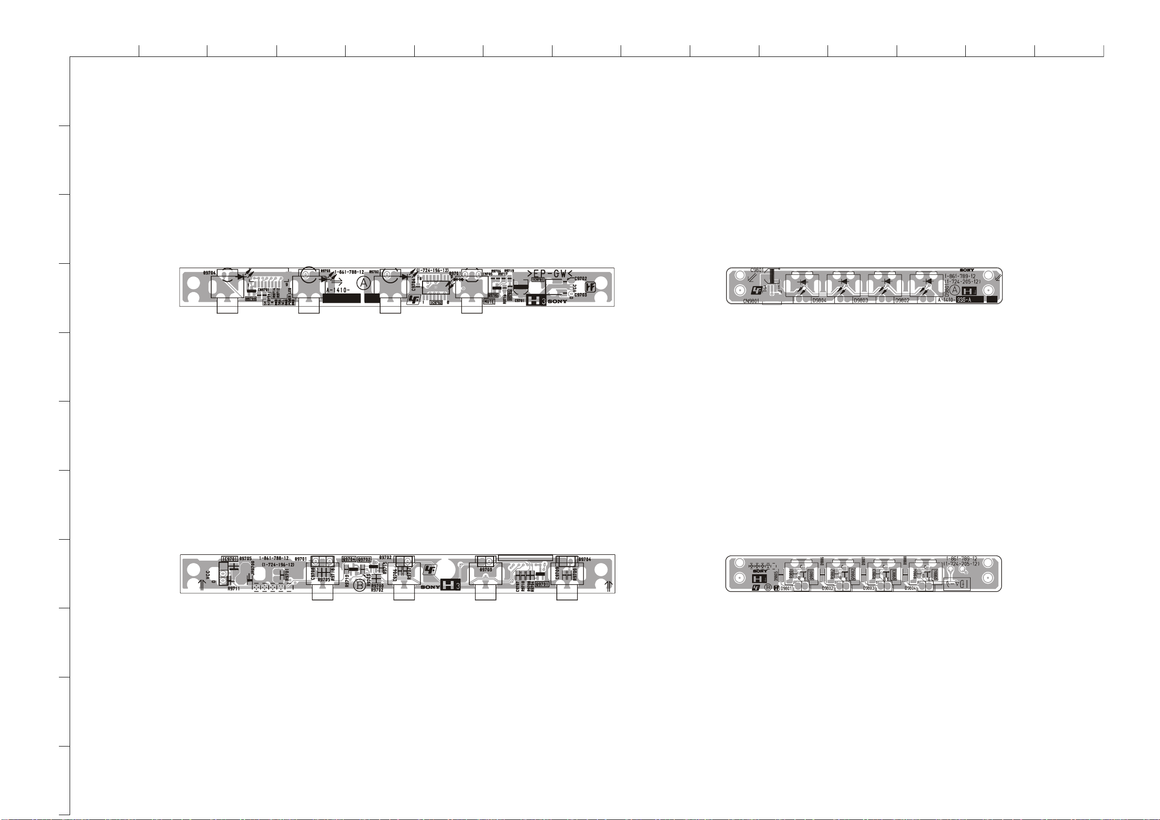
ABCDE F
1
2
3
G
HI JKLMN
O
~ H3 Printed Wiring Board Conductor Side A ~
4
5
6
7
~ H4 Printed Wiring Board Conductor Side A ~
10
11
~ H3 Printed Wiring Board Conductor Side B ~
8
9
~ H4 Printed Wiring Board Conductor Side B ~
- 36 -
Page 37
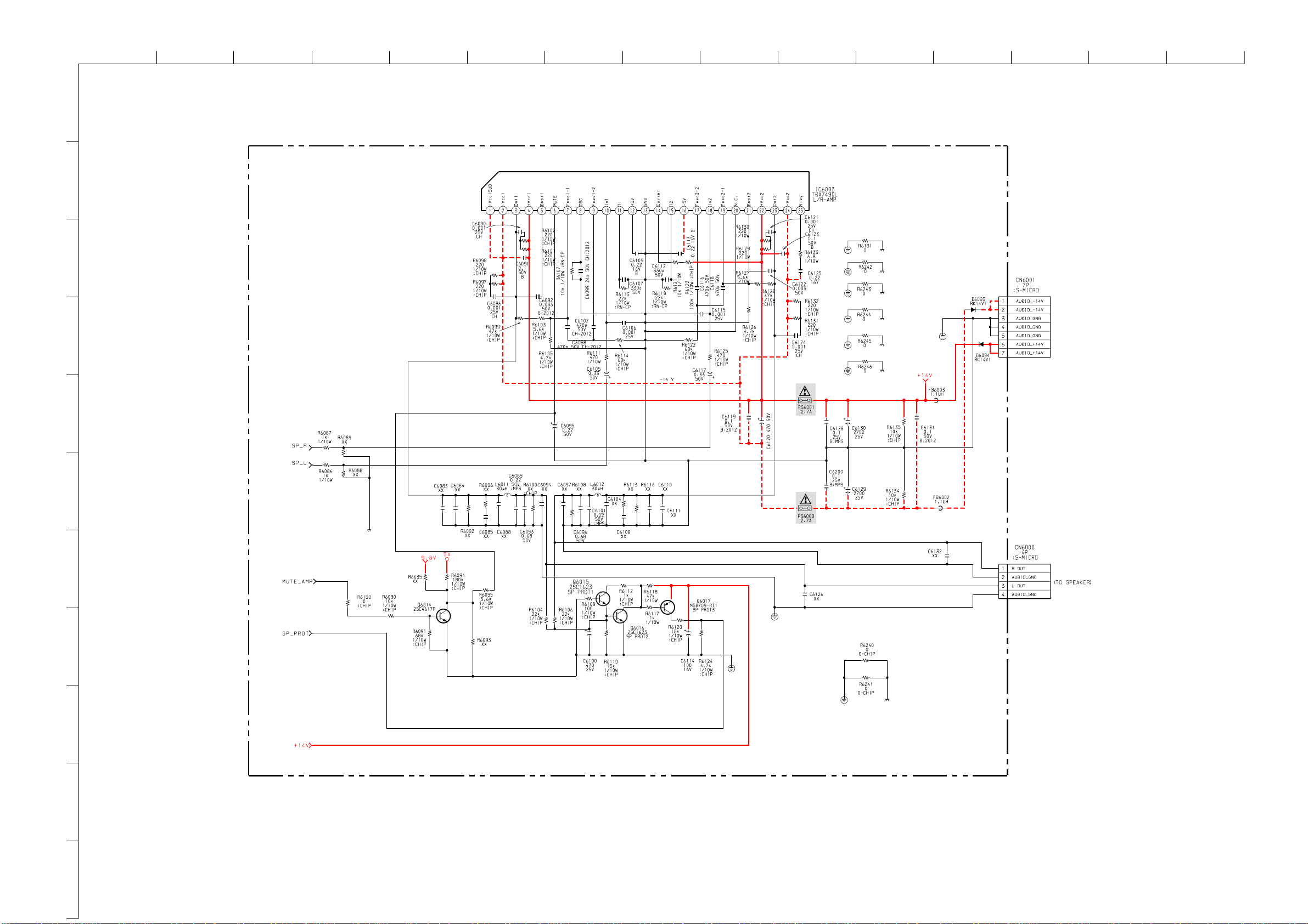
ABCDE F
1
U1.-XS1
2
G
HI JKLMN
O
3
4
5
6
7
U1 1/6
INPUT TERMINAL, AV SW, AUDIO
10
11
8
9
COMPONENTS MARKED AS XX ARE NOT FITTED ON THIS MODEL
~ U1 Board Schematic Diagram [ Input Terminal, AV SW, Audio ] Page 1/6 ~
- 37 -
Page 38
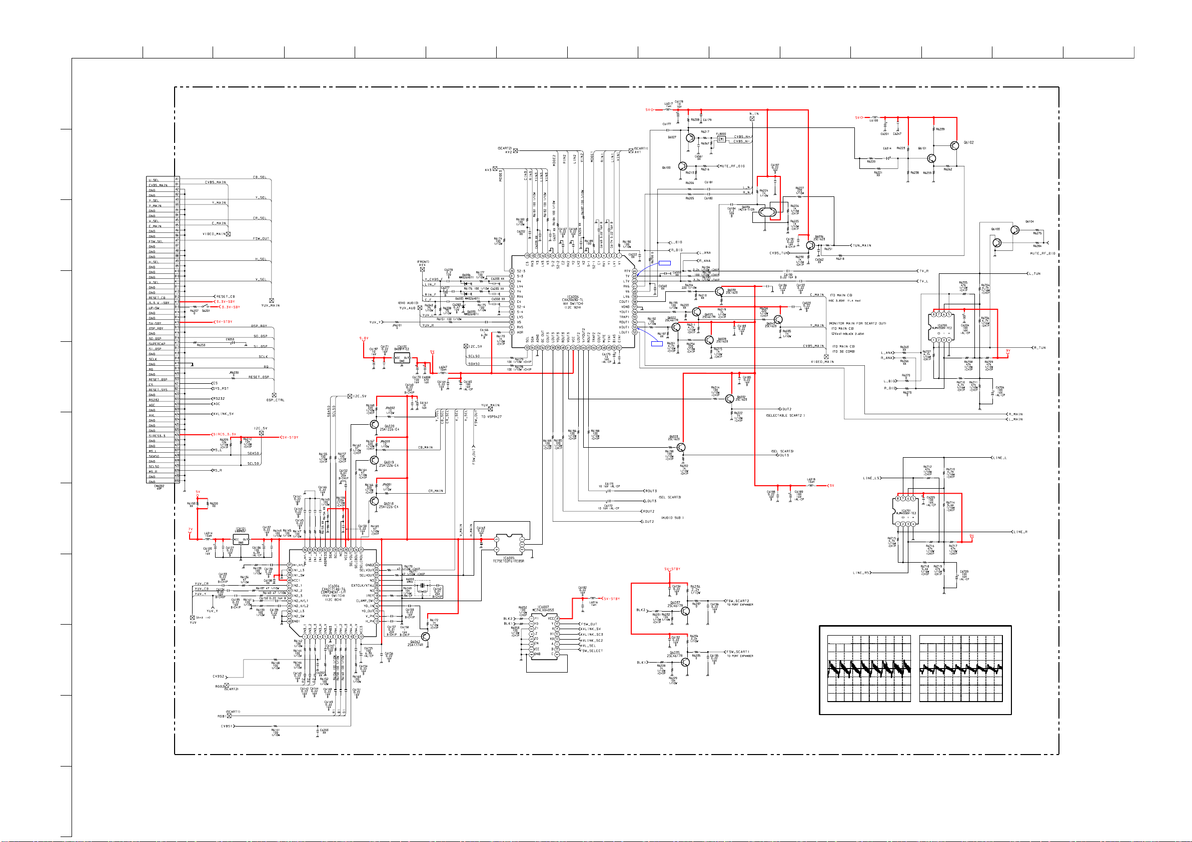
ABCDE F
G
HI JKLMN
O
U1-XS1
1
0.22
2.2K
2.2
2SA1774R
U1
2
2/6
2SC1623-L5L6
0
75
2.2K
2.2K
0.22
2.2K
0.22
2.2K
1UH
0.22
47
6.3V
15K
100
6.3V
0
2SC4617R
15K
470
2SA1774R
470
470
3
XX
TP2
100
2SC3642A
2SC3624A
2.2K
2.2K
4
0.22 5.5V
220
C6176
TP1
0.22
16V
5
6
10
11
7
8
U1(2/6) Board Waveforms
TP1
50us/div
TP2
9
420mVp-p (H) 235mVp-p (H)
COMPONENTS MARKED AS XX ARE NOT FITTED ON THIS MODEL
50us/div
~ U1 Board Schematic Diagram [ Input Terminal, AV SW, Audio ] Page 2/6 ~
- 38 -
Page 39
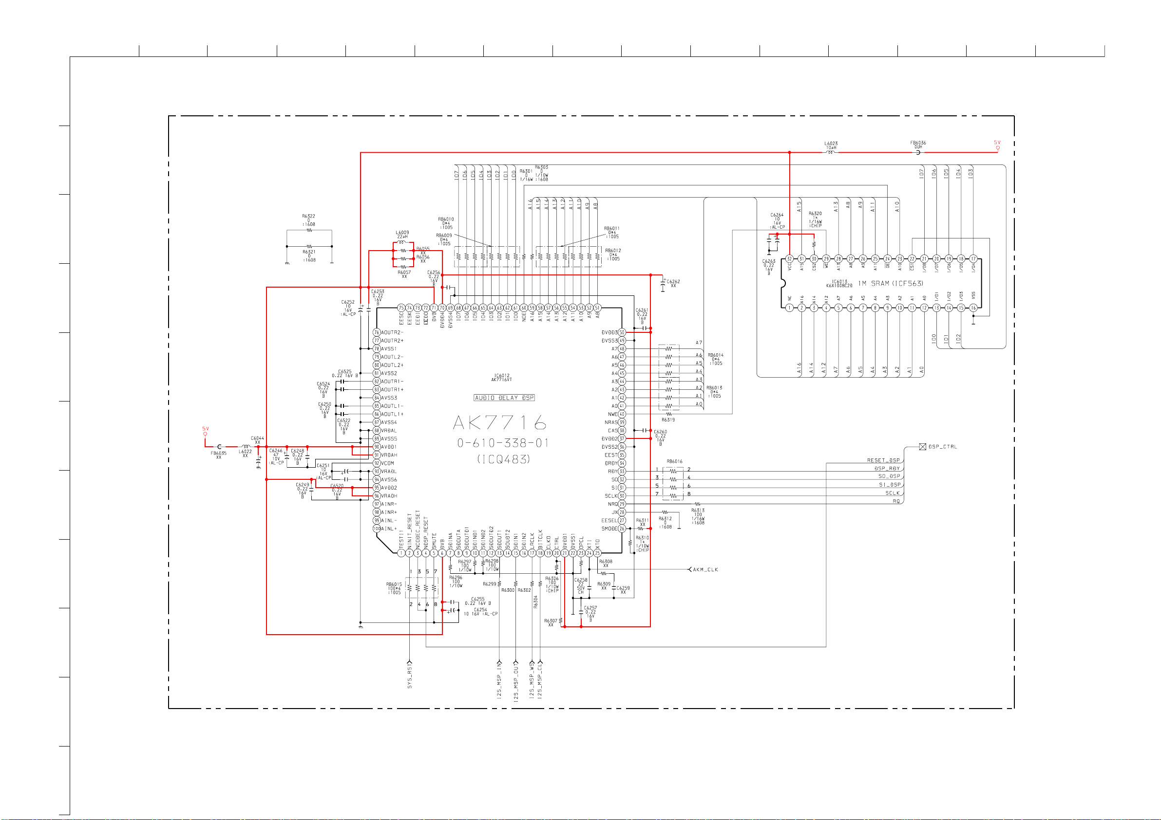
ABCDE F
G
HI JKLMN
O
1
U1.-XS1
2
U1 3/6
3
4
5
100
6
7
8
0UH
0UH
0UH
0UH
9
10
11
COMPONENTS MARKED AS XX ARE NOT FITTED ON THIS MODEL
~ U1 Board Schematic Diagram [ Input Terminal, AV SW, Audio ] Page 3/6 ~
- 39 -
Page 40
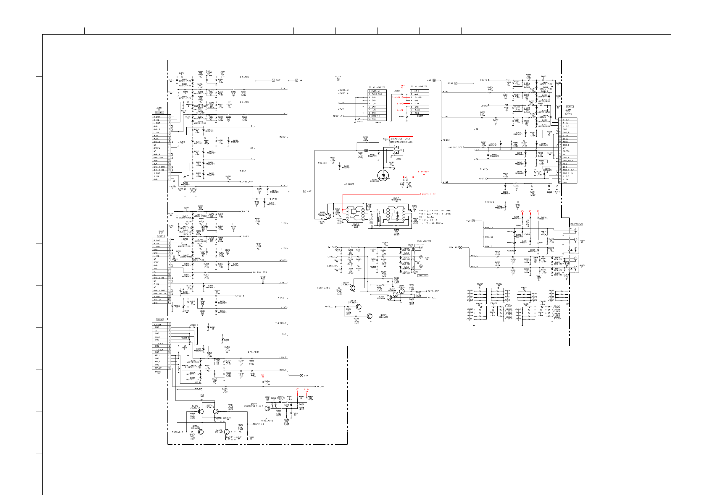
ABCDE F
G
HI JKLMN
O
1
2
U1.-XS1
JR6004
0
0
8P
0
10P
0
3
4
5
0.1
0.1
0.1
10
6
7
U1
4/6
8
TO H2 BOARD
CN9601
COMPONENTS MARKED AS XX ARE NOT FITTED ON THIS MODEL
9
11
~ U1 Board Schematic Diagram [ Input Terminal, AV SW, Audio ] Page 4/6 ~
- 40 -
Page 41
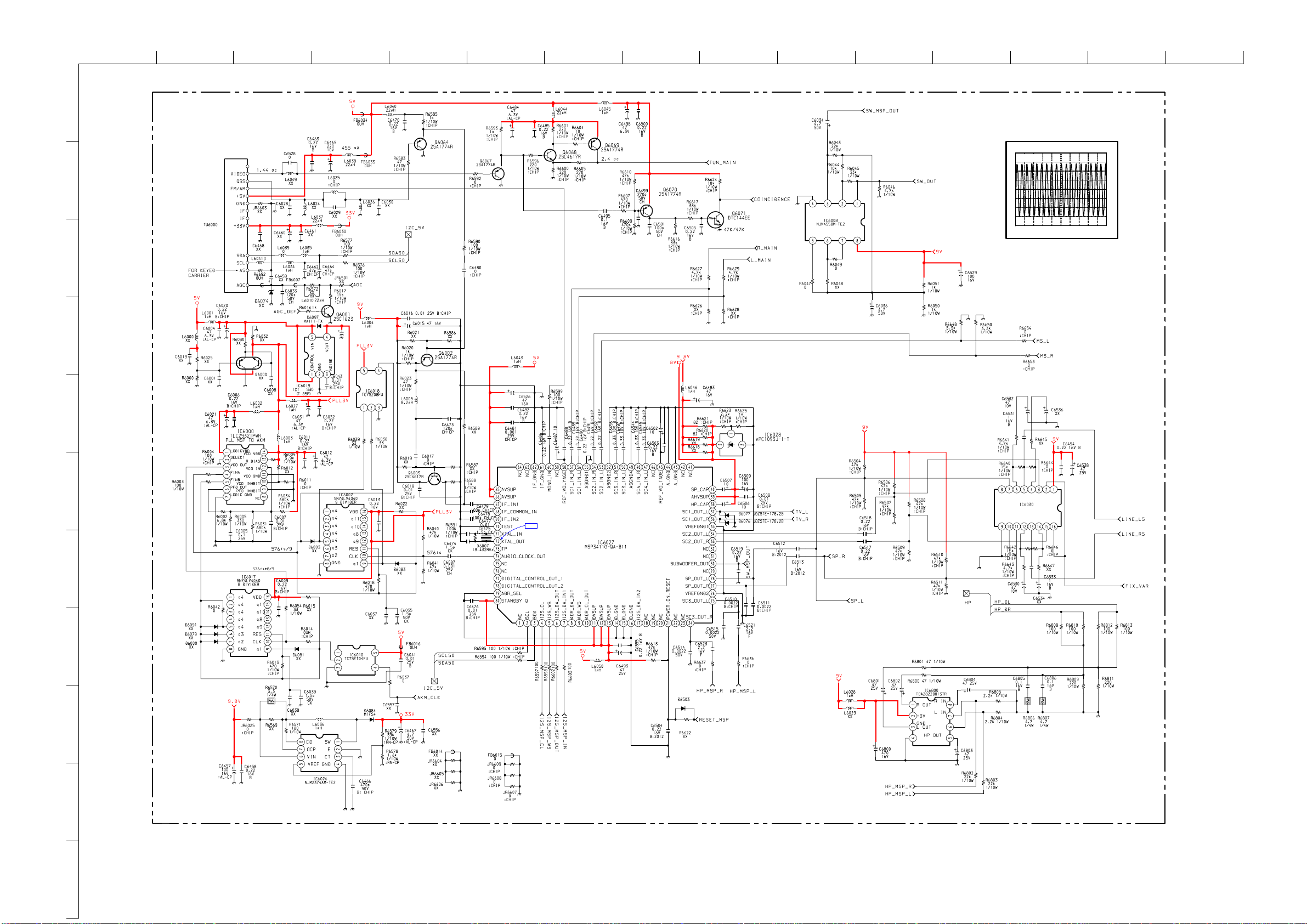
ABCDE F
U1.-XS1
G
HI JKLMN
O
1
U1(5/6) Board Waveform
TP1
100ns/div
2
BTF-EU611
2.9Vp-p (H)
3
0UH
FB6037
0UH
4
AR5
E
C6042
2.2
50V
5
10
6
NJM2123M
TP1
7
8
MA111-TX
9
U1 5/6
COMPONENTS MARKED AS XX ARE NOT FITTED ON THIS MODEL
11
~ U1 Board Schematic Diagram [ Input Terminal, AV SW, Audio ] Page 5/6 ~
- 41 -
Page 42
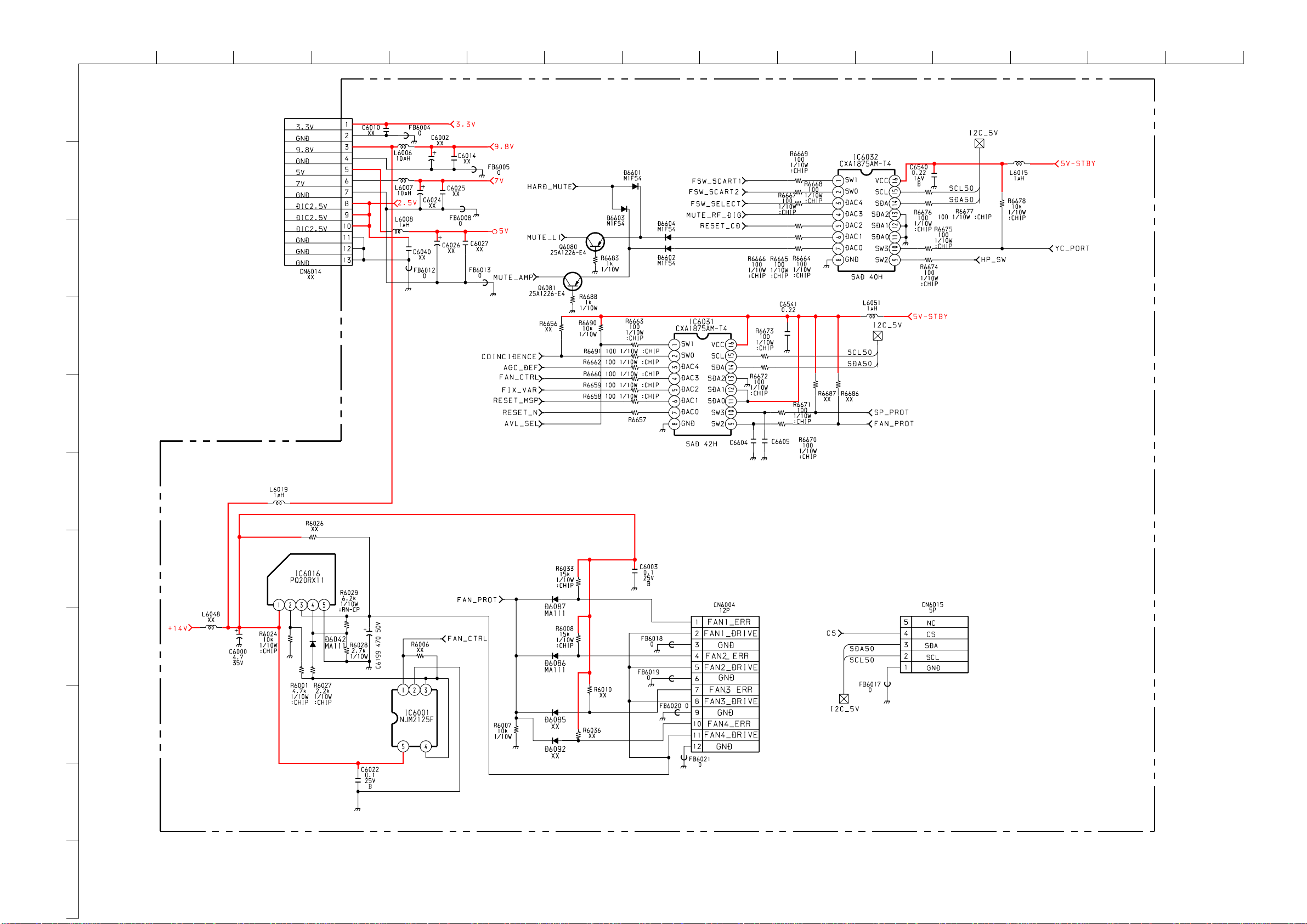
ABCDE F
U1.-XS1
G
HI JKLMN
O
1
+
+
2
+
+
3
4
5
100
0.1
0.1
10
6
U1 6/6
7
8
9
11
COMPONENTS MARKED AS XX ARE NOT FITTED ON THIS MODEL
~ U1 Board Schematic Diagram [ Input Terminal, AV SW, Audio ] Page 6/6 ~
- 42 -
Page 43
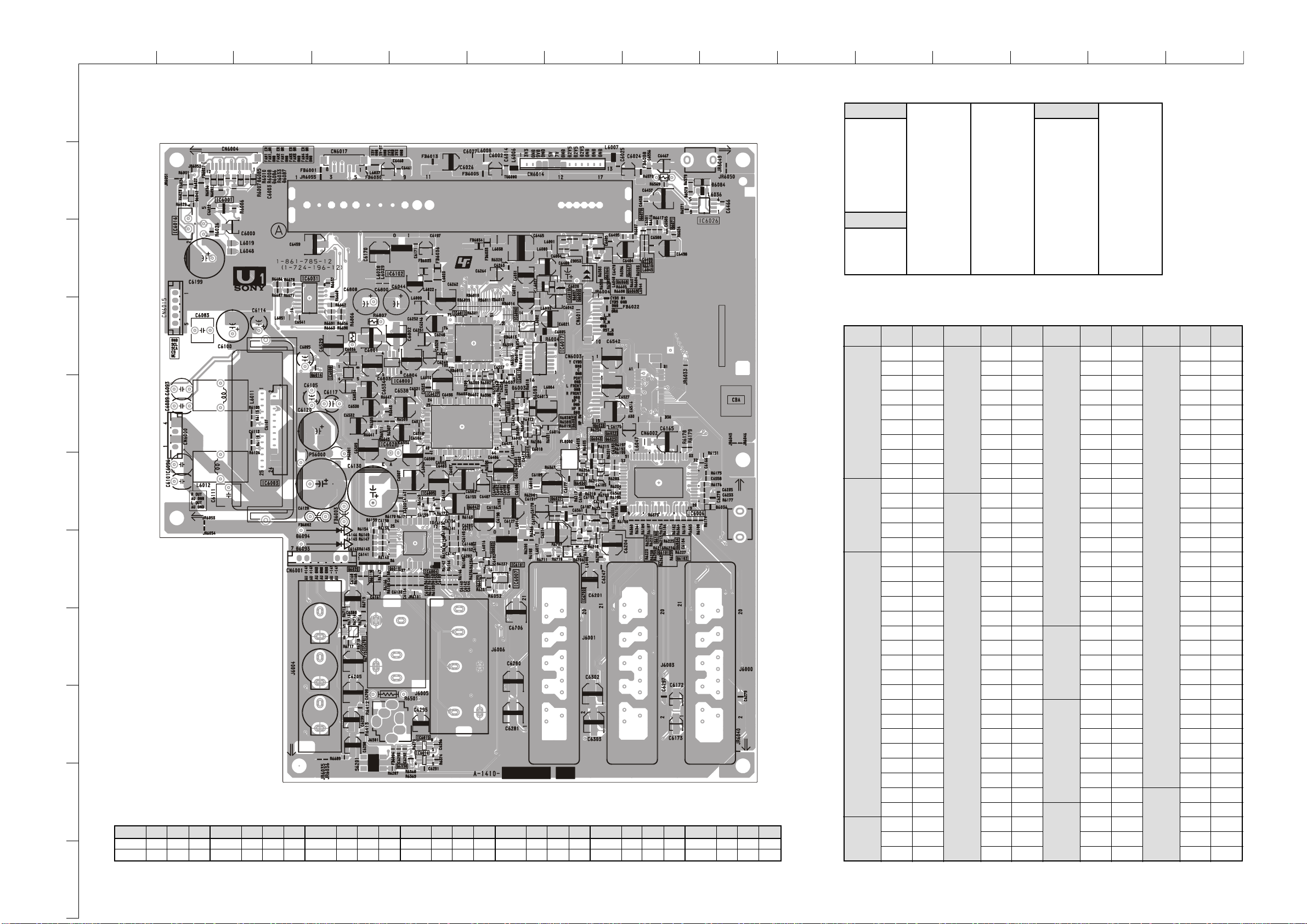
ABCDE F
EDOID
4006CI7-E8106CI5-F
ROTSISNART
4306Q7-H
6306D6-I5006CI6-E9106CI3-G2006Q5-G5306Q7-F
2406D2-B6006CI6-H6206CI2-I3006Q5-F7306Q7-E
4806D2-I7006CI7-F7206CI5-E4106Q4-D8306Q01-D
6806D2-C8006CI4-D8206CI5-D8106Q7-E2406Q6-E
7806D2-C0106CI4-F1306CI3-C9106Q7-D3406Q5-G
7906D4-G2106CI4-E1016CI7-F0206Q7-D4606Q3-G
CI
4106CI9-E2016CI3-E2206Q5-G7606Q3-G
0006CI4-F5106CI9-E0076CI7-G5206Q5-G8606Q3-G
1006CI2-B6106CI3-B1076CI8-D8206Q5-G9606Q3-H
3006CI6-C7106CI4-G0086CI5-E0306Q6-G1706Q2-H
oNfeR
oNniP )V(stloV
feR
oN
oNniP )V(stloV
feR
oN
oNniP )V(stloV
feR
oN
oNniP )V(stloV
0006CI
10.3
6006CI
255.4
2106CI
051.5
7206CI
31-110.5
20 357.435-150 02-410
34.1455.4451.5129.4
5-40 558.3550 03-420
64.1653.375-651.543-338.3
11-70 750 95-850 530
214.1853.4061.573-638.3
313.2955.496-160 830.7
410.3064.417-071.517-071.5
1006CI
19.346-165.4870 939.7
20
8006CI
3-15.4180 040.7
39.340 38-285.244-340
49.37-55.4480 84-548.3
57.981.968-585.2940
4006CI
3-19.2
2106CI
4-21.598-780 15-058.3
5.41.150 19-091.5250
60 6 1.5295.245-358.3
9-79.251-70 49-390 550
11-011.1715.269-591.575-658.3
210.5813.2
6106CI
17.9856.2
41-314.2020 2 6.2068.3
510.2121.539.626-160
614.232-220 46.266-561.5
710.5426.250 86-765.1
810.1523.2
7106CI
50 07-960
020.382-620 7-65.127-174.2
42-220 13-920.580370
62-520.163-230 95.1476.2
727.0731.5014.197-770
820.5041.5112.0081.5
927.4140 610.3
0086CI
11.4
030 241.5
7206CI
3-24.421.9
5006CI
3-10 44-340 43.231.4
40.574-541.555.253.5
50.594-840 7-60 83.5
G
HI JKLMN
O
~ U1 Board Semiconductor Location Table Side A ~
1
~ U1 Printed Wiring Board Conductor Side A ~
2
3
~ U1 Board IC Voltage Table ~
4
5
6
7
8
9
10
11
~ U1 Board Semiconductor Voltage Table ~
feR )s()e( )g()b( )d()c( feR )s()e( )g()b( )d()c( feR )s()e( )g()b( )d()c( feR )s()e( )g()b( )d()c( feR )s()e( )g()b( )d()c( feR )s()e( )g()b( )d()c( feR )s()e( )g()b( )d()c(
2006Q4.38.20 4106Q005.05206Q7.23.31.90306Q7.33.41.93406Q0.27.21.97606Q6.29.10 1706Q1.59.49.0
3006Q8.24.31.92206Q7.23.31.98206Q5.31.41.92406Q6.20.20 4606Q7.21.20 8606Q9.16.24.42706Q6.20.20
- 43 -
Page 44
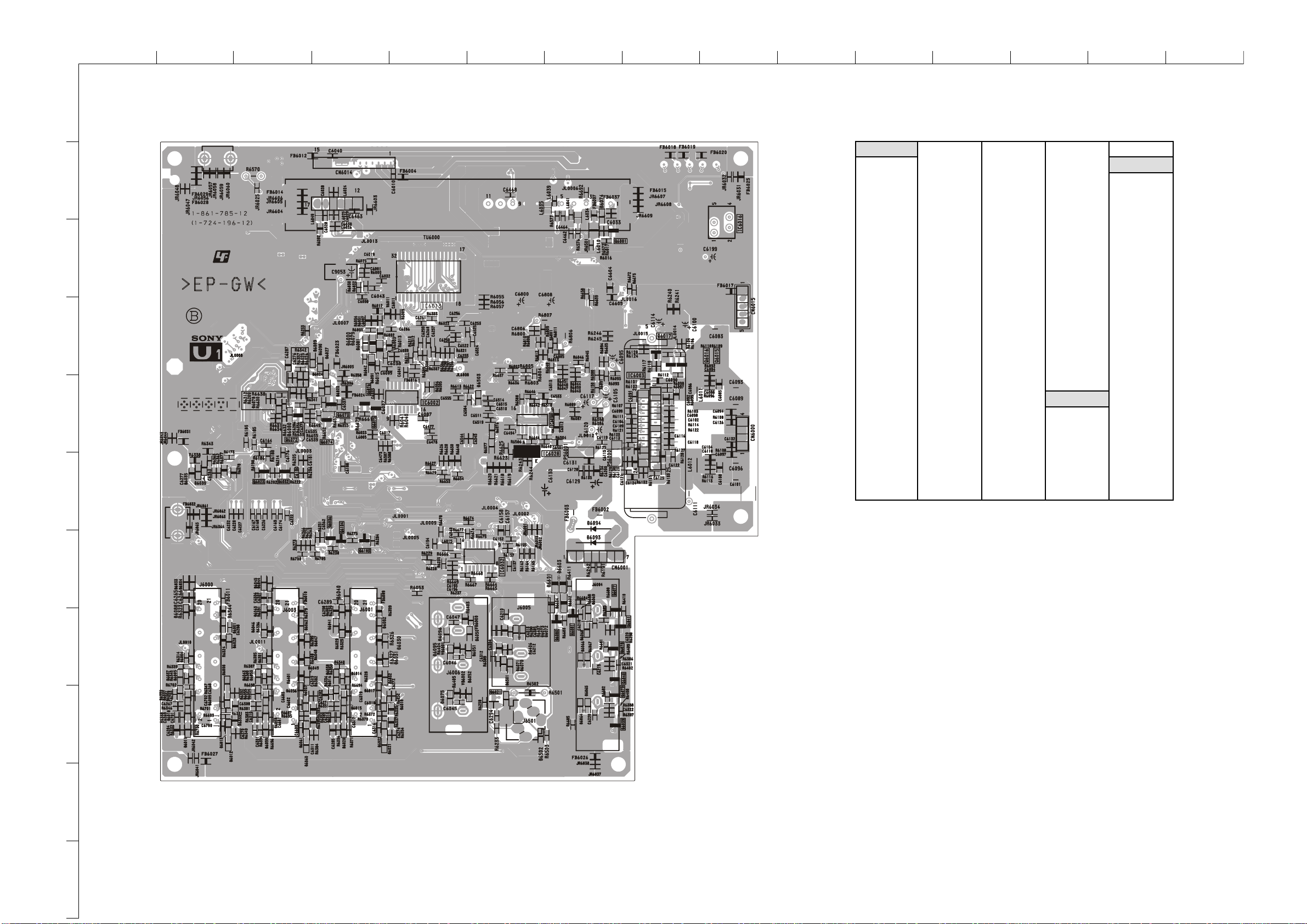
ABCDE F
EDOID
5206D4-C1506D8-E6706D5-F2306CI7-F
1006D8-B6206D4-D2506D8-E7706D5-F
ROTSISNART
4006D8-B7206D4-D3506D8-E0806D5-C1006Q3-G
5006D8-B8206D8-B4506D9-C2806D8-D5106Q4-I
6006D9-B9206D8-D5506D9-C3906D7-G6106Q4-I
7006D9-B0306D8-D6506D8-C4906D6-G7106Q4-H
8006D8-B1306D8-D7506D8-C5906D8-E1206Q9-F
9006D8-B2306D8-D8506D9-C6906D8-E3206Q6-C
0106D9-B3306D7-B9506D9-C1036D8-C2306Q6-C
1106D9-B4306D7-B0606D9-C1056D8-F6306Q6-D
2106D9-B7306D8-B1606D9-C2056D9-F9306Q9-G
3106D9-B8306D8-D2606D8-D3056D4-F0406Q8-G
4106D8-D9306D6-B4606D9-B1066D7-F1406Q8-G
5106D9-D0406D7-D5606D9-B2066D8-G2706Q5-C
6106D8-D1406D8-D6606D8-G3066D5-F3706Q5-D
7106D9-D3406D8-C7606D8-G4066D8-F4706Q5-D
8106D9-D4406D7-C8606D8-G
CI
5706Q5-D
9106D9-D5406D7-C9606D8-G2006CI5-E6706Q5-D
0206D9-D6406D8-C0706D8-F3006CI4-H7706Q8-G
1206D9-D7406D8-C1706D8-F3106CI3-E8706Q5-G
2206D9-D8406D8-C2706D8-F6106CI2-I9706Q8-G
3206D5-D9406D8-C3706D8-F8206CI5-F0806Q8-F
4206D4-D0506D8-E5706D9-E0306CI5-F1806Q8-G
G
HI JKLMN
O
1
~ U1 Printed Wiring Board Conductor Side B ~ ~ U1 Board Semiconductor Location Table Side B ~
2
3
4
5
6
7
8
9
10
11
- 44 -
Page 45
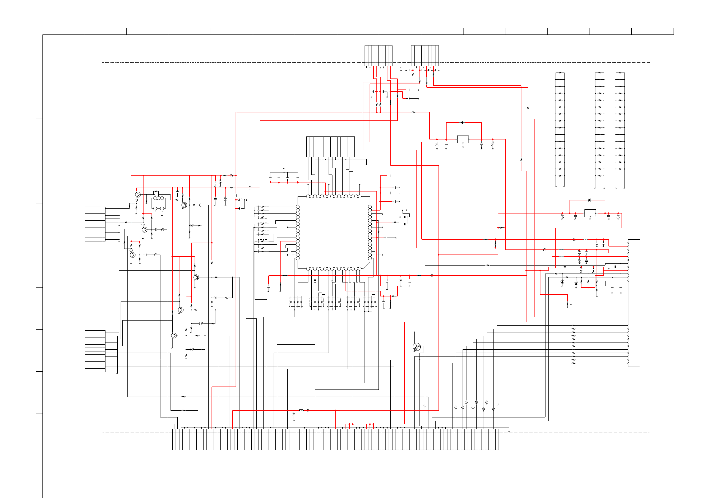
ABCDE F
1
2
3
4
5
6
7
8
9
10
BRN
10P
CN7001
CVBS_N
CVBS_GND
GND
GND
L_N
GND
R_N
GND
RESET_N
GND
1 2 3 4 5 6 7 8 9 10111213141516
1718192021
22
29282726252423
303132
33343536373839404142434445464748
495051525354555657585960616263
64
THC63LVD103
IC7000
TD5
GND
TD6
TE0
TE1
TE2
VCC
TE3
TE4
GND
TE5
CLKIN
/PDWN
PLL GND
PLL VCC
TE6
LVDS GND
TE+
TE-
TD+
TD-
TCLK+
TCLK-
TC+
TC-
LVDS GND
LVDS VCC
TB+
TB-
TA+
TA-
LVDS GND
TA0
TA1
TA2
TA3
TA4
TA5
GND
TA6
TB0
TB1
RS
TB2
TB3
TB4
GND
TB5
TB6
TC0
VCC
TC1
TC2
TC3
TC4
GND
TC5
TC6
TD0
R/F
TD1
TD2
TD3
TD4
2SA1037AK
Q7005
XX
Q7004
XX
Q7003
XX
R7024
XX
R7026
XX
R7021
XX
R7011
XX
R7013
1k
R7016
XX
R7032
XX
R7025
XX
C7003
XX
C7004
XX
C7005
XX
C7008
XX
R7028
XX
R7029
XX
R7027
XX
R7033
2SA1037AK-T146-QR
Q7000
XX
R7030
XX
R7031
XX
R7023
XX
R7022
XX
R7019
XX
R7020
XX
R7017
XX
R7018
1/10W
1k
R7004
1/10W
1k
R7000
1/10W
15k
R7007
1/10W
15k
R7002
10k
R7003
10V
1
C7000
1
2
3
4
5
6
7
8
9
10
11
12
BRN
12P
CN7000
Y_N_BKP
GND
CR_N_BKP
GND
CB_N_BKP
GND
FBLK_N_BKP
GND
DPI_SDA
GND
DPI_SCL
GND
123456789
1011121314
14P
CN7002
LV_D+
LV_D-
DRAIN
LV_CLK+
LV_CLK-
DRAIN
LV_C+
LV_C-
DRAIN
LV_B+
LV_B-
DRAIN
LV_A+
LV_A-
16V
0.22
C7015
16V
0.22
C7024
16V
0.22
C7019
16V
0.22
C7023
0.22
C7018
1uH
L7005
1/10W
100k
R7039
XX
C7027
CHIP
0
R7035
16V
0.22
C7013
XX
R7034
XX
R7038
CHIP
0
R7037
16V
0.22
C7020
6.3V
100
C7010
16V
1000
C7009
16V
0.22
C7007
16V
0.22
C7006
10MH
L7000
22uH
L7001
A1
B1
A2B2A3
B3
A4
A5
A6
B4
B5
B6
A7
B7
A8
B8
A9
B9
A10
B10
A11
B11
A12
B12
A13
B13
A14
B14
A15
B15
A16
B16
A17
B17
A18
B18
A19
B19
A20
B20
A21
B21
A22
B23
B27
B24
B25
A28
B28
A29
B29
A24
A25
A26
A23
A30
B30
B26
A27
C7
C12
A32C1A31
B31
C14
C15
C2
C8
C11
B32
C10
C5
C16
C9
C13
C6
B22
C3
C4
C21
C20
C17
C19
C18
C24
C23
C22
C27
C25
C30
C29
C26
C28
C31
C32
96P
CN7004
IN_TS[0]
IN_TS[2]
IN_TS[4]
IN_TS[6]
IN_TSCLK
GND-D
SCL_N
FE_RESET
IN-TSEN
GND-D
SCL-TV
GND-D
+3V3D
GND-D
+2V5D
GND-D
PWR_DWN
GND-D
JIGMODE
EIVHS
YC_C
EIVVS
VD_HSYNC
VDO[6]
VDO[4]
VDO[2]
VDO[0]
GND-A
GND-A
GND-A
GND-A
GND-A
GND-A
GND-A
LEFT
LNBTONE
18/13V
NOT_LNBOVR
LNBON
SPDIF
GND-D
NOT_N_RESET
YC_Y/ANA-ALPHA
TS_SELECT
GND-D
TXD4B
CSEL/EFBLANK1
GND-D
GND-A
GND-D
YUV_Y/YC_Y
GND-D
YUV_U/YC_C
+3V3D
YUV_V
GND-D
CVBS_OUT
+2V5D
FASTBLK
+5VD
GND-A
GND-D
RIGHT
VD_CLK
IN_TS[1]
GND-D
IN_TS[3]
VD_VSYNC
IN_TS[5]
VDO[7]
IN_TS[7]
VDO[5]
IN_TSPSYNC
VDO[3]
GND_D
VDO[1]
SDA_N
GND-A
RSLOCK
+5V A
RXD4B
GND-A
GND-D
+12 V
SDA_TV
GND-A
GND-D
MODE/EFBLANK3
+3V3D
GND-A
GND-D
AUDIO_MUTE/EFBLANK2
+2V5D
+5VD
GND-D
GND-D
1uH
L7014
1uH
L7017
1uH
L7015
1uH
L7016
50V
2.2
C7041
XX
C7044
XX
C7043
XX
C7047
XX
C7045
6.3V
100
C7040
6.3V
100
C7042
6.3V
100
C7046
XX
R7067
XX
R7068
1/10W
100
R7015
1/10W
100
R7014
1/10W
100
R7043
CHIP
0
R7042
XX
R7050
100
R7051
1/10W
100
R7052
UDZS-TE17-12B
D7003
UDZS-TE17-12B
D7002
XX
R7065
XX
R7066
RB7004
100
1
2
345
6
7
8
RB7003
100
1
2
345
6
7
8
RB7005
100
1
2
345
6
7
8
RB7006
100
1
2
345
6
7
8
RB7007
100
1
2
345
6
7
8
RB7000
100
1
2
3
4
5
6
7
8
RB7002
100
1
2
3
4
5
6
7
8
RB7001100
1
2
3
4
5
6
7
8
10MH
L7002
16V
1000
C7011
B1 +5V
VC +32V
AGC MONI
PRESET
(+1.8V)
+3.3V
PD0/
PD2
PD4
PD6
PDOCLK
SDA
SCL
AS
PD3
PD5
PD7
PDOERR/
PDSYNC
PD1
PDOVAL
NC
+5V
NC
SPLITTER
(PDSERIAL)
(RSLOCK)
TU7000
0
R7053
0
R7054
0
R7055
0R7056
0R7057
0R7058
0R7059
0
R7060
0R7061
0
R7062
0R7063
0
R7064
16V
0.22
C7012
XX
Q7006
123
46
FL7000
XX
R7009
Q7001
1/10W
1k
R7001
5.6k
R7005
1/10W
560
R7012
16V
0.22
C7002
25V
0.01
C7022
25V
0.01
C7016
6.3V
10
C7021
25V
1000p
CH
C7025
25V
1000p
C7017
6.3V
10
C7014
100
R7036
XX
C7049
XX
C7050
XX
C7048
DTC144EK
Q7007
TP7010
1234567
8
WHT
8P
CN7005
ATSC +5V
ATSC +5V
GND
GND
ATSC +9V
ATSC +9V
GND
GND
1234567
8
8P
CN7007
+33V
GND
+5V-SBY
GND
+2.5V
GND
+3.3V
GND
0
R7071
0
R7072
XX
R7074
150
R7069
TP7011
0uH
FB001
0uH
FB002
0uH
FB003
0uH
FB004
0uH
FB005
0uHFB006
0uH
FB007
0uH
FB008
0uH
FB009
0uH
FB010
16V
0.1
C7051
JR7042
0
JR7043
0
JR7044
0
JR7045
0
JR7046
0
JR7047
0
JR7048
0
JR7049
0
JR7050
0
JR7051
0
JR7052
0
JR7053
0
JR7054
0
JR7055
0
JR7041
0
JR7040
0
XX
JR7001
XX
JR7002
XX
JR7003
XX
JR7004
XX
JR7005
XX
JR7006
XX
JR7007
XX
JR7008
XX
JR7009
XX
JR7010
XX
JR7011
XX
JR7012
XX
JR7013
XX
JR7014
XX
JR7015
XX
JR7016
XX
JR7017
XX
JR7018
XX
JR7019
XX
JR7020
XX
JR7021
XX
JR7022
XX
JR7023
XX
JR7024
XX
JR7025
XX
JR7026
XX
JR7027
XX
JR7028
XX
JR7029
XX
JR7030
XX
JR7031
CHIP
0
JR7107
0
JR7106
0
JR7108
0
JR7109
16V
0.01
C7052
16V
0.01
C7053
0.01
C7054
0.01
C7055
0
JR7102
0
JR7103
0
JR7104
0
JR7105
0.01
C7056
16V
0.01
C7057
16V
0.01
C7058
16V
0.01
C7059
6.3V
100
C7026
2SA1037AK
Q7002
10k
R7008
10V
1
C7001
TO A4 BOARD
N1.-XS1
N1
COMPONENTS MARKED AS XX ARE NOT FITTED TO THIS MODEL
DIGITAL TUNER
TO APS202 BOARD
CN9008 CN6017
TO U1 BOARD
BTD-DU606Z
CN4103
16V
TO A4 BOARD
CN4104
TO U1 BOARD
CN6011
2SC1623-L5L6
TO N BOARD
MA111-TX
D7004
VCC
GND
OUT
BA033FP-E2
IC7001
16V
0.1
C7064
16V
0.1
C7063
0uH
FB7040
16V
10
C7062
6.3V
100
C7065
0uH
FB7039
XX
C7067
XX
C7068
XX
C7066
XX
C7069
VCC
GND
OUT
XX
IC7002
XX
D7005
XX
R7082
0uH
FB7036
0uH
FB7035
0uH
FB7021
0uH
FB7011
0
R7075
0uH
FB7012
0
R7076
0uH
FB7010
0
R7077
0uH
FB7006
0uH
FB7013
0uH
FB7037
16V
1000
C7060
10MH
L7018
0uH
FB7038
25V
0.001
C7061
G
HI JKLMN
O
1
2
3
4
5
6
7
8
9
10
11
~ N1 Board Schematic Diagram [ Digital Tuner ] ~
- 45 -
Page 46
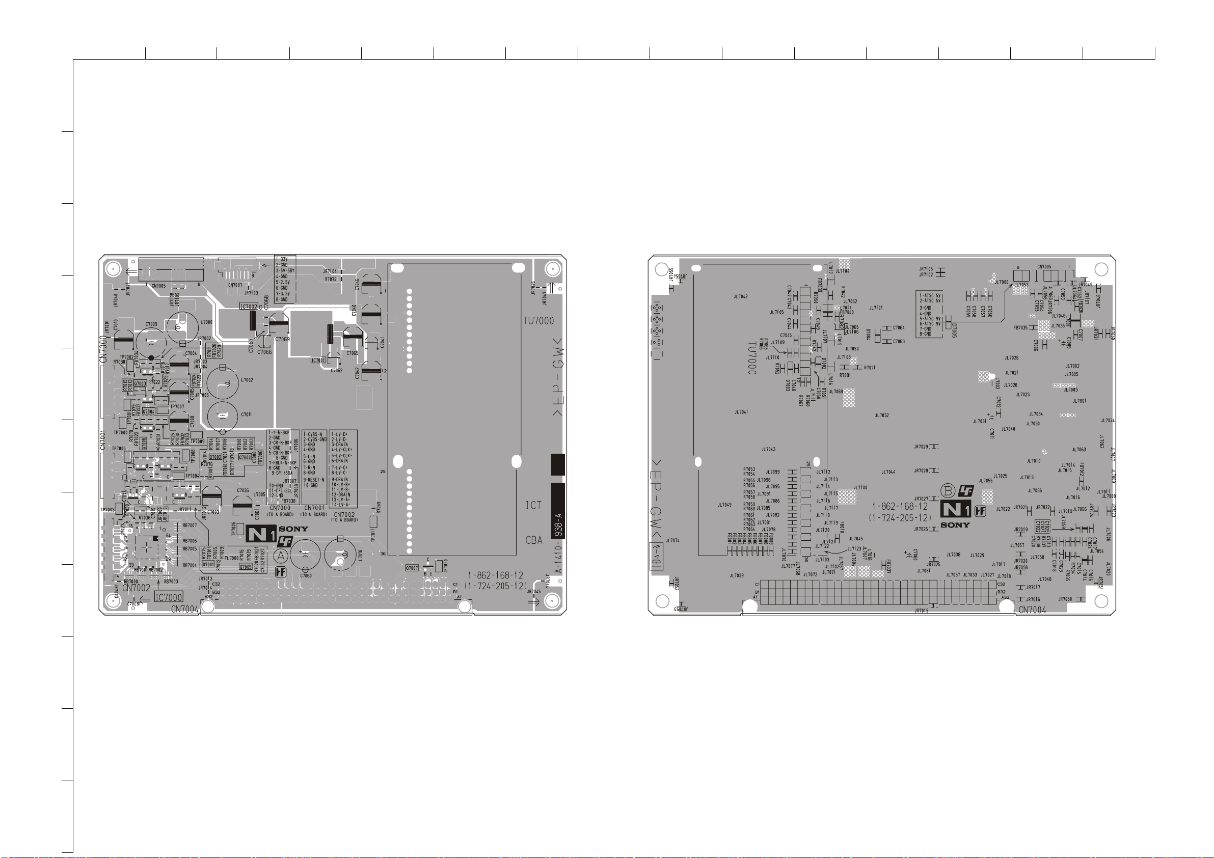
ABCDE F
1
2
G
HI JKLMN
O
3
4
5
6
7
~ N1 Printed Wiring Board Conductor Side A ~
~ N1 Printed Wiring Board Conductor Side B ~
10
11
8
9
- 46 -
Page 47
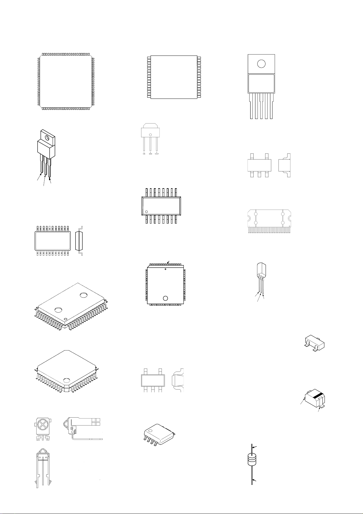
1
100
25
26 50
51
75
76
4-4. SEMICONDUCTORS
XS1
RM-Y1011
IC AK7716VT
IC BA09FP-E2
IN
OUT
GND
IC CXA1875AM-T4
IC NJM4558V-TE2
IC TDA2822D013TR
IC TLC2932IPWR
IC K6X1008C2D-BF70T
1
16
IC L88M05T-FA-TL
IC MC74LVXT4053DTR2
IC NJM2123M (T1)
16 9
1
( TOP VIEW )
8
IC PQ20RX11J00H
32
17
IC TAR5S30(TE85R)
IC TDA7490L
1
TOP VIEW
IC MSP3411G-QA-B11
68
1
9
10
61
60
IC UPC1093J-1-T
IC CXA2069Q-TL
18
26
( TOP VIEW )
52
44
433527
REF
ANODE
CATHODE
2SA1037AK-T146-R
IC CXA2171AQ-T6
IC NJM2125F(TE2)
IC TC7SET02FU(TE85R)
IC TC7SET04FU(TE85R1)
IC TC7SZ08FU(TE85R)
2SA1162-G
2SC1623-L5L6
DTC144EE
MSB709-RT1
C
B
E
MA111-TX
MM3Z12VT1
MM3Z3V9T1
MM3Z6V8T1
IC GP1UM27SRK
IC NJM2374AM-TE2
IC TC7WH00FU(TE12R)
IC TC7WHU04FU(TE12R)
1
7
6
5
2
3
4
MMDL914T1
UDZ-TE-17-8.2B
UDZS-TE17-12B
RK14V1
CATHODE
ANODE
CATHODE
ANODE
- 47 -
Page 48
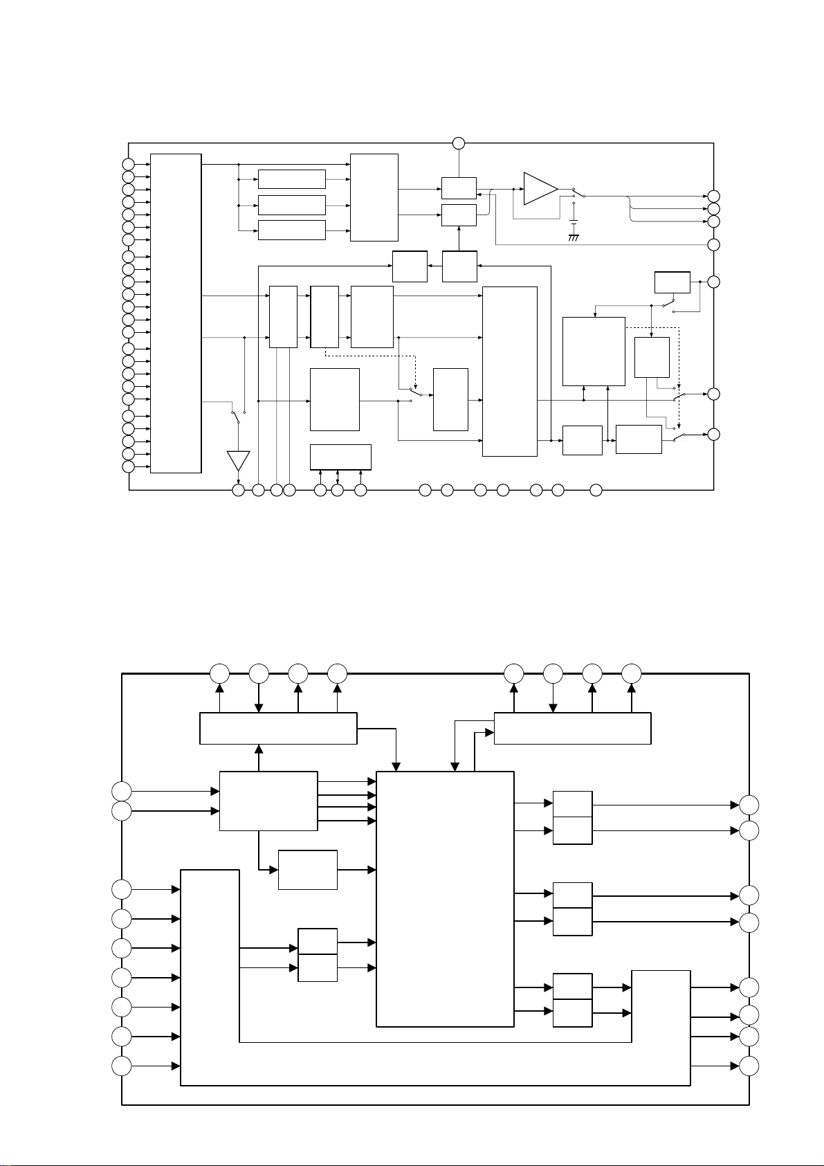
4-5 IC BLOCK DIAGRAMS
27
SELY_OUT
26
SELCB_OUT
25
SELCR_OUT
17
CLP_SW
20
EXTCLK/XTAL
18
IREF
29
CLP_CR
40
Vcc1
48
GND1
28
Vcc2
24
GND2
12
Vcc3
6
GND3
23
SELV_OUT
33
IN1_1
34
IN1_2
35
IN1_3
36
IN1_H/L1
37
IN1_V/L2
38
IN1_L3
39
IN1_SW
6dB
PEAK
HOLD
LEVEL
DET.
POLARITY
DISTINCT.
V SYNC
SEP.
SYNC
SEP.
I2C bus
DEC.
YPbPr → YCbCr
(CCIR)
MATRIX
SELECTOR
YPbPr → YCbCr
(BTA)
RGB → YCbCr
41
IN2_1
42
IN2_2
43
IN2_3
44
IN2_H/L1
45
IN2_V/L2
46
IN2_L3
47
IN2_SW
1
IN3_1
2
IN3_2
3
IN3_3
4
IN3_H
5
IN3_V
7
IN4_1
8
IN4_2
9
IN4_3
10
IN4_H
11
15 16 13 14
IN4_V
IN1 `IN4
SELECTOR
∗ INPUT_SEL (2)
∗ SELSTB_1 (1)
∗ SELSTB_2 (1)
+ DECL1_1 (2)
+ DECL2_1 (2)
+ DECL3_1 (2)
+ DECSW_1 (1)
+ DECL1_2 (2)
+ DECL2_2 (2)
+ DECL3_2 (2)
DECSW_2 (1)
+ EH (1)
+ EV (1)
∗ HD_TC (1)
∗ HSEP_SEL (1)
∗ V_TC (2)
∗ MAT_OUT (2)
+3-STATE (1)
∗ YGAIN (4)
∗ CBGAIN (4)
∗ CRGAIN (4)
∗ CLK_SEL (1)
∗ GAIN_SEL (2)
Y Y/Cb/Cr
Cb/Cr
10
H
V
H SYNC
WIDTH
MACRO
VISION
22
SELH_OUT
DUMMY
SYNC
CLOCK
GEN.
CLAMP
CLAMP
CLP
&
3SYNCP
3STATE
SYNC
DET.
H_PH
YG_IN
YG_OUT
V_PH
∗ HYSW (1)
SYNC
COUNTER
PRIORITY
RANK
HV > CS > Y/G
6dB
AMP.
H
V
H
V
H
V
0
1
0
1
2, 3
0
1
2
3
∗ H_WIDTH (2)
∗ MACRO (1)
∗ HS_MASK (1)
∗ FIX_SYNC (2)
∗ SELDUM (1)
+ H_NUMBER_H (2)
+ H_NUMBER_L (8)
+ V_NUMBER_H (2)
+ V_NUMBER_L (8)
30 31 32
SCL
SDA
ADDRESS
U1 BOARD IC6004 CXA2171AQ-T6
XS1
RM-Y1011
U1 BOARD IC6027 MSP3411G
25
23
28
31
30
34
33
37
36
65 68 13 45 7 6
SBUS Interface
DEMODULATOR
IDENT
DFP
A/D
- 48 -
A/D
SCART Switching Facilities
I2C Interface
D/A
D/A
D/A
D/A
D/A
D/A
56
57
59
60
47
48
50
51
Page 49
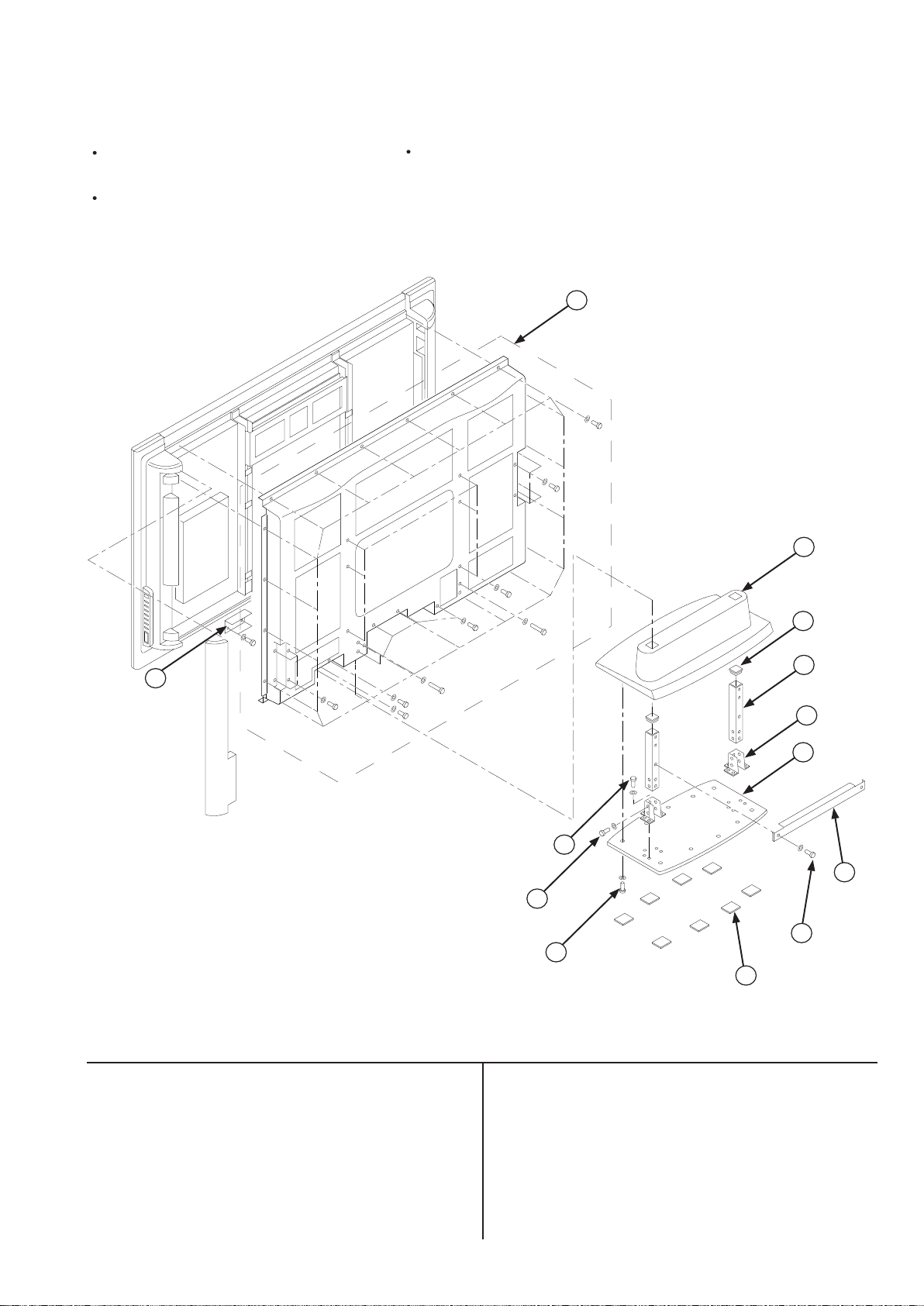
XS1
RM-Y1011
SECTION 5
EXPLODED VIEWS
NOTE :
Items with no part number and no description are not
stocked because they are seldom required for routine
service.
The construction parts of an assembled part are indicated
with a collation number in the remarks column.
Items marked “*” are not stocked
since they are seldom required for
routine service. Some delay should
be anticipated when ordering these
items.
5-1. REAR COVER AND STAND
REF.NO. PART.NO DESCRIPTION REMARK REF.NO. PART.NO DESCRIPTION REMARK
- 49 -
1 X-2021-896-2 COVER, REAR (37) ASSY (KDE-P37XS1) 2
X-2021-895-2 COVER, REAR (42) ASSY (KDE-P42XS1) 2
2 4-102-644-01 COVER (42), STAND BASE PAINTED
3 4-098-263-01 CAP (42), STAND
4 4-098-260-01 FRAME (42A), STAND BASE
5 4-098-262-03 BRACKET (42), STAND BASE
6 4-098-259-02 PLATE (42), STAND BASE
7 4-098-261-01 FRAME (42B), STAND BASE
8 *4-098-264-01 CUSHION A
9 *7-682-000-07 SCREW +PSW M5X12
10 7-682-973-09 SCREW +PSW 5X8
11 7-685-647-79 SCREW +BVTP 3X10 TYPE2 IT-3
12 *X-4043-041-1 BRACKET, RF ASSY
2
3
4
5
6
7
8
1
9
10
11
12
o
7-685-663-79
SCREW +BVTP 4X16 TYPE2 IT-3
m
7-682-947-09
SCREW +PSW 3X6
s
7-682-962-09
SCREW +PSW 4X10
u
7-682-973-19
SCREW +PSW 5X10
o
m
s
u
o
o
o
o
m
10
m
Page 50
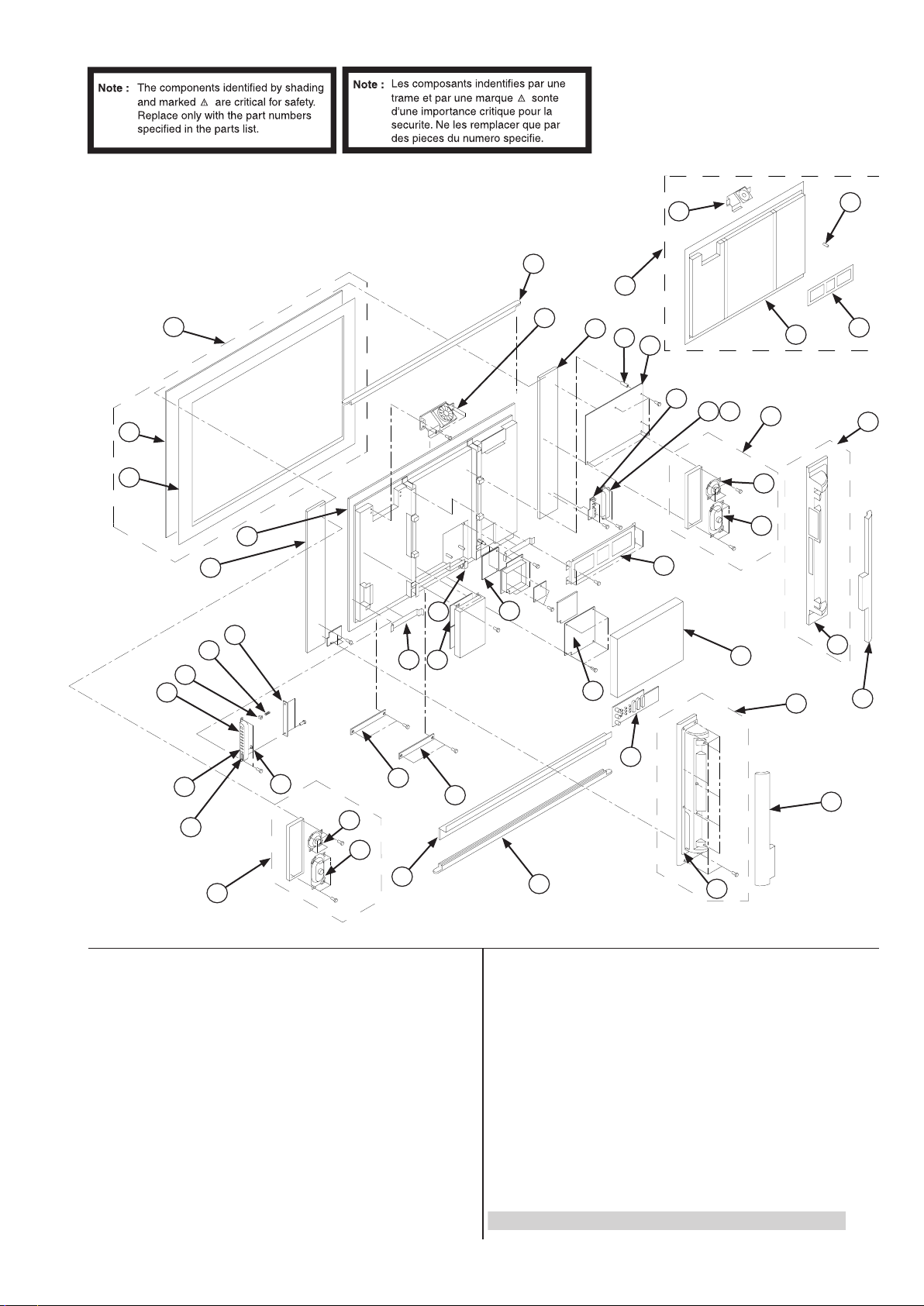
XS1
RM-Y1011
5-2. DISPLAY PANEL, BOARDS, AND SPEAKERS
REF.NO. PART.NO DESCRIPTION REMARK REF.NO. PART.NO DESCRIPTION REMARK
- 50 -
51 A-1606-650-A FRONT, PANEL ASSY (KDE-P37XS1) 52-53
A-1606-645-A FRONT, PANEL ASSY (KDE-P42XS1) 52-53
52 1-758-986-21 GLASS, OPTICAL FILTER (KDE-P37XS1)
1-758-985-21 GLASS, OPTICAL FILTER (KDE-P42XS1)
53 4-098-128-11 SHEET (FG) (KDE-P37XS1)
4-098-128-01 SHEET (FG) (KDE-P42XS1)
54 *1-805-365-21 PLASMA DISPLAY PANEL (KDE-P37XS1)
*1-805-349-11 PLASMA DISPLAY PANEL (KDE-P42XS1)
55 4-102-271-01 BOX SPEAKER(37 FRONT-R)PAINTED(KDE-P37XS1)
4-102-235-01 BOX SPEAKER(42 FRONT-R)PAINTED(KDE-P42XS1)
56 *A-1415-623-A H1 BOARD, COMPLETE
57 *4-098-112-01 SPRING, COMPRESSION
58 4-102-231-01 BUTTON, POWER
59 4-102-232-11 COVER, CONTROL PANEL PRINTED
60 4-098-111-12 ORNAMENT (MS)
61 X-4042-973-1 BUTTON MULTI ASSY
62 *4-098-110-01 GUIDE LIGHT (MS)
63 A-1606-623-A SPEAKER (37R) ASSY (KDE-P37XS1) 64-65
A-1606-608-A SPEAKER (42R) ASSY (KDE-P42XS1) 64-65
64 1-825-610-12 LOUDSPEAKER (5CM)
65 1-825-609-11 LOUDSPEAKER (5.5X12CM)
66 X-4042-983-1 FILTER GLASS BRACKET(37)ASSY (KDE-P37XS1)
X-4042-968-1 FILTER GLASS BRACKET(42)ASSY (KDE-P42XS1)
67 X-4042-760-3 BAR (BOTTOM) 37 ASSY (KDE-P37XS1)
X-4042-754-3 BAR (BOTTOM) 42 ASSY (KDE-P42XS1)
68 *A-1415-626-A H4 BOARD, COMPLETE
69 *A-1410-934-A H3 BOARD, COMPLETE
70 *4-098-165-01 CLAMPER
71 *A-1410-938-A N1 BOARD, COMPLETE
72 £ *1-816-517-21 INLET, AC (WITH NOISE FILTER)
81
52
56
53
54
57
58
59
61
63
64
65
66
67
68
69
72
73
75
77
85
86
87
92
93
84
55
62
78
70
74
76
80
83
88
89
90
60
l
l
l
7-685-648-79 SCREW +BVTP 3X12 TYPE2 IT-3
o
7-685-663-79 SCREW +BVTP 4X16 TYPE2 IT-3
u
4-678-370-01 SCREW (M3X8), CROSS (HOLE) PAN
s
3-703-136-11 SCREW, TAPPING
m
7-682-947-09 SCREW +PSW 3X6
o
o
o
u
m
l
m
m
m
m
l
l
l
l
l
s
51
79
82
64
65
91
92
89
54
84
71
Page 51

XS1
RM-Y1011
REF.NO. PART.NO DESCRIPTION REMARK REF.NO. PART.NO DESCRIPTION REMARK
- 51 -
73 *A-1302-996-A MS2A BOARD, COMPLETE
74 X-2022-022-1 BRACKET, U-PWB (D) ASSY
75 *A-1302-881-A U1 BOARD, COMPLETE
76 *3-919-255-01 HOLDER, PC BOARD
77 X-4042-985-2 SPEAKER REAR (37R) ASSY (KDE-P37XS1) 78
X-4042-970-2 SPEAKER REAR (42R) ASSY (KDE-P42XS1) 78
78 4-102-273-02 BOX SPEAKER(37 REAR-R)PAINTED (KDE-P37XS1)
4-102-215-02 BOX SPEAKER(42 REAR-R)PAINTED (KDE-P42XS1)
79 X-4042-987-1 SPEAKER COVER (37R) ASSY (KDE-P37XS1)
X-4042-972-1 SPEAKER COVER (42R) ASSY (KDE-P42XS1)
80 X-4042-984-1 SPEAKER REAR (37L) ASSY (KDE-P37XS1) 81
X-4042-969-1 SPEAKER REAR (42L) ASSY (KDE-P42XS1) 81
81 4-102-272-01 BOX SPEAKER (37 REAR-L)PAINTED(KDE-P37XS1)
4-102-214-01 BOX SPEAKER (42 REAR-L)PAINTED(KDE-P42XS1)
82 X-4042-986-1 SPEAKER COVER (37L) ASSY (KDE-P37XS1)
X-4042-971-1 SPEAKER COVER (42L) ASSY (KDE-P42XS1)
83 A-1606-622-A SPEAKER (37L) ASSY (KDE-P37XS1) 64-65
A-1606-607-A SPEAKER (42L) ASSY (KDE-P42XS1) 64-65
84 4-098-215-02 MAIN FRM (37) ASSY (KDE-P37XS1)
4-098-145-02 MAIN FRM (42) ASSY (KDE-P42XS1)
85 4-098-094-03 LID (CONNECTOR PANEL)
86 4-102-233-01 COVER, CONNECTOR PANEL PAINTED
87 *A-1415-624-A H2 BOARD, COMPLETE
88 1-468-794-31 REGULATOR, SWITCHING
89 4-087-569-02 SPACER
90 4-102-270-01 BOX SPEAKER (37 FRONT-L)PAINTED(KDE-P37XS1)
4-102-220-01 BOX SPEAKER (42 FRONT-L)PAINTED(KDE-P42XS1)
91 A-1606-627-A PANEL ASSY (KDE-P37XS1) 54, 84, 89, 92
A-1606-612-A PANEL ASSY (KDE-P42XS1) 54, 84, 89, 92
92 1-763-659-11 FAN, DC
93 X-4043-029-1 BAR (TOP, 37D) ASSY
X-4043-026-1 BAR (TOP, 42D) ASSY
Page 52

SECTION 6
ELECTRICAL PARTS LIST
PARTS LISTING TABLE OF CONTENTS
Note : Items marked “*” are not stocked since they are seldom required for routine service.
Some delay should be anticipated when ordering these items.
Parts indicated (XX) on the Schematic Diagram are not used in this model and
therefore do not appear in the Parts List.
- 52 -
H1 BOARD COMPLETE Parts List : .................................................................................................... 53
H2 BOARD COMPLETE Parts List : .................................................................................................... 53
N1 BOARD COMPLETE Parts List : .................................................................................................... 53
H3 BOARD COMPLETE Parts List : .................................................................................................... 55
H4 BOARD COMPLETE Parts List : .................................................................................................... 56
U1 BOARD COMPLETE Parts List : .................................................................................................... 56
MISCELLANEOUS : .................................................................................................... 67
ACCESSORIES AND PACKAGING MATERIALS : ...................................................................................... 67
REMOTE COMMANDER: .................................................................................................... 67
Page
Page 53
REF.NO. PART.NO DESCRIPTION REMARK REF.NO. PART.NO DESCRIPTION REMARK
- 53 -
* A-1415-623-A H1 Board Complete
< CAPACITOR >
C9501 1-107-826-11 CERAMIC CHIP 0.1UF 10.00% 16V
C9502 1-117-681-11 ELECT CHIP 100UF 20.00% 16V
C9503 1-162-974-11 CERAMIC CHIP 0.01UF 50V
C9504 1-162-974-11 CERAMIC CHIP 0.01UF 50V
C9505 1-107-826-11 CERAMIC CHIP 0.1UF 10.00% 16V
< CONNECTOR >
CN9501 1-770-624-21 PIN, CONNECTOR 7P
< DIODE >
D9501 8-719-083-82 DIODE UDZS-TE17-12B
D9502 8-719-083-82 DIODE UDZS-TE17-12B
< RESISTOR >
R9501 1-216-809-11 METAL CHIP 100 5% 1/10W
R9503 1-216-864-11 SHORT CHIP 0
R9505 1-216-864-11 SHORT CHIP 0
R9510 1-216-833-11 METAL CHIP 10K 5% 1/10W
R9511 1-216-829-11 METAL CHIP 4.7K 5% 1/10W
R9512 1-216-841-11 METAL CHIP 47K 5% 1/10W
R9513 1-216-833-11 METAL CHIP 10K 5% 1/10W
R9514 1-216-809-11 METAL CHIP 100 5% 1/10W
R9515 1-216-829-11 METAL CHIP 4.7K 5% 1/10W
R9520 1-216-864-11 SHORT CHIP 0
< SWITCH >
S9501 1-572-595-11 SWITCH, TACTIL (REFLOW TYPE)
S9502 1-572-595-11 SWITCH, TACTIL (REFLOW TYPE)
S9503 1-572-595-11 SWITCH, TACTIL (REFLOW TYPE)
S9504 1-572-595-11 SWITCH, TACTIL (REFLOW TYPE)
S9505 1-572-595-11 SWITCH, TACTIL (REFLOW TYPE)
S9506 1-554-419-00 SWITCH, PUSH (1 KEY)
S9507 1-572-595-11 SWITCH, TACTIL (REFLOW TYPE)
S9508 1-572-595-11 SWITCH, TACTIL (REFLOW TYPE)
* A-1415-624-A H2 Board Complete
< CONNECTOR >
CN9601 1-695-209-21 PIN, CONNECTOR (PC BOARD) 15P
< DIODE >
D9600 8-719-083-82 DIODE UDZS-TE17-12B
D9601 8-719-083-82 DIODE UDZS-TE17-12B
D9602 8-719-083-82 DIODE UDZS-TE17-12B
D9603 8-719-083-82 DIODE UDZS-TE17-12B
D9604 8-719-083-82 DIODE UDZS-TE17-12B
D9605 8-719-083-82 DIODE UDZS-TE17-12B
D9606 8-719-083-82 DIODE UDZS-TE17-12B
D9607 8-719-083-82 DIODE UDZS-TE17-12B
D9608 8-719-083-82 DIODE UDZS-TE17-12B
D9609 8-719-083-82 DIODE UDZS-TE17-12B
D9610 8-719-083-82 DIODE UDZS-TE17-12B
D9611 8-719-083-82 DIODE UDZS-TE17-12B
D9612 8-719-083-82 DIODE UDZS-TE17-12B
< SOCKET >
J9600 1-568-267-11 JACK
J9601 1-565-666-12 TERMINAL, S 4P
J9602 1-580-443-11 JACK, PIN 3P
< RESISTOR >
R9600 1-216-809-11 METAL CHIP 100 5% 1/10W
R9601 1-216-809-11 METAL CHIP 100 5% 1/10W
R9602 1-216-809-11 METAL CHIP 100 5% 1/10W
R9603 1-216-864-11 SHORT CHIP 0
R9604 1-216-864-11 SHORT CHIP 0
R9605 1-216-864-11 SHORT CHIP 0
R9606 1-216-864-11 SHORT CHIP 0
< VARISTOR >
VD9602 1-803-974-21 VARISTOR, CHIP (1608)
* A-1410-938-A N1 Board Complete
< CAPACITOR >
C7000 1-115-156-11 CERAMIC CHIP 1UF 10V
C7001 1-115-156-11 CERAMIC CHIP 1UF 10V
C7002 1-127-715-91 CERAMIC CHIP 0.22UF 10% 16V
C7006 1-127-715-91 CERAMIC CHIP 0.22UF 10% 16V
C7007 1-127-715-91 CERAMIC CHIP 0.22UF 10% 16V
C7009 1-126-767-11 ELECT CHIP 1000UF 20.00% 16V
C7010 1-126-206-11 ELECT CHIP 100UF 20.00% 6.3V
C7011 1-126-767-11 ELECT CHIP 1000UF 20.00% 16V
C7012 1-127-715-91 CERAMIC CHIP 0.22UF 10% 16V
C7013 1-127-715-91 CERAMIC CHIP 0.22UF 10% 16V
C7014 1-137-710-11 CERAMIC CHIP 10UF 20% 6.3V
C7015 1-127-715-91 CERAMIC CHIP 0.22UF 10% 16V
C7016 1-162-970-11 CERAMIC CHIP 0.01UF 10.00% 25V
C7017 1-115-416-11 CERAMIC CHIP 0.001UF 5.00% 25V
C7018 1-127-715-91 CERAMIC CHIP 0.22UF 10% 16V
C7019 1-127-715-91 CERAMIC CHIP 0.22UF 10% 16V
C7020 1-127-715-91 CERAMIC CHIP 0.22UF 10% 16V
C7021 1-137-710-11 CERAMIC CHIP 10UF 20% 6.3V
C7022 1-162-970-11 CERAMIC CHIP 0.01UF 10.00% 25V
C7023 1-127-715-91 CERAMIC CHIP 0.22UF 10% 16V
N1
H2H1
Page 54

REF.NO. PART.NO DESCRIPTION REMARK REF.NO. PART.NO DESCRIPTION REMARK
- 54 -
C7024 1-127-715-91 CERAMIC CHIP 0.22UF 10% 16V
C7025 1-115-416-11 CERAMIC CHIP 0.001UF 5.00% 25V
C7026 1-126-206-11 ELECT CHIP 100UF 20.00% 6.3V
C7040 1-126-206-11 ELECT CHIP 100UF 20.00% 6.3V
C7041 1-126-601-11 ELECT CHIP 2.2UF 20.00% 50V
C7042 1-126-206-11 ELECT CHIP 100UF 20.00% 6.3V
C7046 1-126-206-11 ELECT CHIP 100UF 20.00% 6.3V
C7051 1-107-826-11 CERAMIC CHIP 0.1UF 10.00% 16V
C7052 1-107-726-91 CERAMIC CHIP 0.01UF 10.00% 16V
C7053 1-107-726-91 CERAMIC CHIP 0.01UF 10.00% 16V
C7054 1-107-726-91 CERAMIC CHIP 0.01UF 10.00% 16V
C7055 1-107-726-91 CERAMIC CHIP 0.01UF 10.00% 16V
C7056 1-162-974-11 CERAMIC CHIP 0.01UF 50V
C7057 1-107-726-91 CERAMIC CHIP 0.01UF 10.00% 16V
C7058 1-107-726-91 CERAMIC CHIP 0.01UF 10.00% 16V
C7059 1-107-726-91 CERAMIC CHIP 0.01UF 10.00% 16V
C7060 1-126-767-11 ELECT CHIP 1000UF 20.00% 16V
C7061 1-115-416-11 CERAMIC CHIP 0.001UF 5.00% 25V
C7062 1-124-779-00 ELECT CHIP 10UF 20.00% 16V
C7063 1-107-826-11 CERAMIC CHIP 0.1UF 10.00% 16V
C7064 1-107-826-11 CERAMIC CHIP 0.1UF 10.00% 16V
C7065 1-126-206-11 ELECT CHIP 100UF 20.00% 6.3V
< CONNECTOR >
CN7000 * 1-764-097-11 PIN, CONNECTOR (PC BOARD) 12P
CN7001 * 1-764-095-11 PIN, CONNECTOR (PC BOARD) 10P
CN7002 * 1-817-752-21 CONNECTOR (RECEPTACLE) 14P
CN7004 1-818-370-11 SOCKET, PC CONNECTOR 96P
CN7005 * 1-564-523-11 PLUG, CONNECTOR 8P
CN7007 * 1-764-093-21 PIN, CONNECTOR (PC BOARD) 8P
< DIODE >
D7002 8-719-083-82 DIODE UDZS-TE17-12B
D7003 8-719-083-82 DIODE UDZS-TE17-12B
D7004 8-719-404-50 DIODE MA111-TX
< FERRITE BEAD >
FB001 1-414-921-11 FERRITE 0UH
FB002 1-414-921-11 FERRITE 0UH
FB003 1-414-921-11 FERRITE 0UH
FB004 1-414-921-11 FERRITE 0UH
FB005 1-414-921-11 FERRITE 0UH
FB006 1-414-921-11 FERRITE 0UH
FB007 1-414-921-11 FERRITE 0UH
FB008 1-414-921-11 FERRITE 0UH
FB009 1-414-921-11 FERRITE 0UH
FB010 1-414-921-11 FERRITE 0UH
FB7006 1-469-835-21 FERRITE 0UH
FB7010 1-469-835-21 FERRITE 0UH
FB7011 1-414-760-21 FERRITE 0UH
FB7012 1-469-835-21 FERRITE 0UH
FB7013 1-469-835-21 FERRITE 0UH
FB7021 1-414-760-21 FERRITE 0UH
FB7035 1-414-921-11 FERRITE 0UH
FB7036 1-414-921-11 FERRITE 0UH
FB7037 1-469-835-21 FERRITE 0UH
FB7038 1-469-835-21 FERRITE 0UH
FB7039 1-414-760-21 FERRITE 0UH
FB7040 1-414-760-21 FERRITE 0UH
< FILTER >
FL7000 1-233-765-21 FILTER
< IC >
IC7000 6-704-519-01 IC THC63LVD103
IC7001 8-759-460-72 IC BA033FP-E2
< COIL >
L7000 1-406-677-11 INDUCTOR 10UH
L7001 1-412-030-11 INDUCTOR 22UH
L7002 1-406-677-11 INDUCTOR 10UH
L7005 1-469-549-21 INDUCTOR 1UH
L7014 1-469-549-21 INDUCTOR 1UH
L7015 1-469-549-21 INDUCTOR 1UH
L7016 1-469-549-21 INDUCTOR 1UH
L7017 1-469-549-21 INDUCTOR 1UH
L7018 1-406-677-11 INDUCTOR 10UH
< TRANSISTOR >
Q7000 8-729-026-49 TRANSISTOR 2SA1037AK-T146-R
Q7001 8-729-120-28 TRANSISTOR 2SC1623-L5L6
Q7002 8-729-026-49 TRANSISTOR 2SA1037AK-T146-R
Q7005 8-729-026-49 TRANSISTOR 2SA1037AK-T146-R
Q7007 1-801-806-11 TRANSISTOR DTC144EKA
< RESISTOR >
JR7040 1-216-864-11 SHORT CHIP 0
JR7041 1-216-864-11 SHORT CHIP 0
JR7042 1-216-864-11 SHORT CHIP 0
JR7043 1-216-864-11 SHORT CHIP 0
JR7044 1-216-864-11 SHORT CHIP 0
JR7045 1-216-864-11 SHORT CHIP 0
JR7046 1-216-864-11 SHORT CHIP 0
JR7047 1-216-864-11 SHORT CHIP 0
JR7048 1-216-864-11 SHORT CHIP 0
JR7049 1-216-864-11 SHORT CHIP 0
JR7050 1-216-864-11 SHORT CHIP 0
JR7051 1-216-864-11 SHORT CHIP 0
JR7052 1-216-864-11 SHORT CHIP 0
JR7053 1-216-864-11 SHORT CHIP 0
JR7054 1-216-864-11 SHORT CHIP 0
N1
Page 55
REF.NO. PART.NO DESCRIPTION REMARK REF.NO. PART.NO DESCRIPTION REMARK
- 55 -
JR7055 1-216-864-11 SHORT CHIP 0
JR7102 1-216-864-11 SHORT CHIP 0
JR7103 1-216-864-11 SHORT CHIP 0
JR7104 1-216-864-11 SHORT CHIP 0
JR7105 1-216-864-11 SHORT CHIP 0
JR7106 1-216-864-11 SHORT CHIP 0
JR7107 1-216-864-11 SHORT CHIP 0
JR7108 1-216-864-11 SHORT CHIP 0
JR7109 1-216-864-11 SHORT CHIP 0
R7000 1-216-821-11 METAL CHIP 1K 5% 1/10W
R7001 1-216-821-11 METAL CHIP 1K 5% 1/10W
R7002 1-216-835-11 METAL CHIP 15K 5% 1/10W
R7003 1-216-833-11 METAL CHIP 10K 5% 1/10W
R7004 1-216-821-11 METAL CHIP 1K 5% 1/10W
R7005 1-216-830-11 METAL CHIP 5.6K 5% 1/10W
R7007 1-216-835-11 METAL CHIP 15K 5% 1/10W
R7008 1-216-833-11 METAL CHIP 10K 5% 1/10W
R7012 1-216-818-11 METAL CHIP 560 5% 1/10W
R7014 1-216-809-11 METAL CHIP 100 5% 1/10W
R7015 1-216-809-11 METAL CHIP 100 5% 1/10W
R7016 1-216-821-11 METAL CHIP 1K 5% 1/10W
R7035 1-216-864-11 SHORT CHIP 0
R7036 1-216-809-11 METAL CHIP 100 5% 1/10W
R7037 1-216-864-11 SHORT CHIP 0
R7039 1-216-845-11 METAL CHIP 100K 5% 1/10W
R7042 1-216-864-11 SHORT CHIP 0
R7043 1-216-809-11 METAL CHIP 100 5% 1/10W
R7051 1-216-809-11 METAL CHIP 100 5% 1/10W
R7052 1-216-809-11 METAL CHIP 100 5% 1/10W
R7053 1-216-864-11 SHORT CHIP 0
R7054 1-216-864-11 SHORT CHIP 0
R7055 1-216-864-11 SHORT CHIP 0
R7056 1-216-864-11 SHORT CHIP 0
R7057 1-216-864-11 SHORT CHIP 0
R7058 1-216-864-11 SHORT CHIP 0
R7059 1-216-864-11 SHORT CHIP 0
R7060 1-216-864-11 SHORT CHIP 0
R7061 1-216-864-11 SHORT CHIP 0
R7062 1-216-864-11 SHORT CHIP 0
R7063 1-216-864-11 SHORT CHIP 0
R7064 1-216-864-11 SHORT CHIP 0
R7069 1-216-811-11 METAL CHIP 150 5% 1/10W
R7071 1-216-864-11 SHORT CHIP 0
R7072 1-216-864-11 SHORT CHIP 0
R7075 1-216-864-11 SHORT CHIP 0
R7076 1-216-864-11 SHORT CHIP 0
R7077 1-216-864-11 SHORT CHIP 0
N1 H3
< RESISTOR CHIP >
RB7000 1-233-576-11 RES, CHIP NETWORK 100 (3216)
RB7001 1-233-576-11 RES, CHIP NETWORK 100 (3216)
RB7002 1-233-576-11 RES, CHIP NETWORK 100 (3216)
RB7003 1-233-576-11 RES, CHIP NETWORK 100 (3216)
RB7004 1-233-576-11 RES, CHIP NETWORK 100 (3216)
RB7005 1-233-576-11 RES, CHIP NETWORK 100 (3216)
RB7006 1-233-576-11 RES, CHIP NETWORK 100 (3216)
RB7007 1-233-576-11 RES, CHIP NETWORK 100 (3216)
< TUNER >
TU7000 8-598-638-00 TUNER UNIT, DIGITAL BTD-DU606Z
* A-1410-934-A H3 Board Complete
4-091-676-01 HOLDER (A), LED
< CAPACITOR >
C9701 1-126-205-11 ELECT CHIP 47UF 20.00% 6.3V
C9702 1-164-156-11 CERAMIC CHIP 0.1UF 25V
C9703 1-164-230-11 CERAMIC CHIP 220PF 5.00% 50V
C9704 1-127-715-91 CERAMIC CHIP 0.22UF 10% 16V
C9705 1-164-156-11 CERAMIC CHIP 0.1UF 25V
C9706 1-164-156-11 CERAMIC CHIP 0.1UF 25V
C9707 1-164-156-11 CERAMIC CHIP 0.1UF 25V
C9708 1-164-156-11 CERAMIC CHIP 0.1UF 25V
C9709 1-164-156-11 CERAMIC CHIP 0.1UF 25V
< CONNECTOR >
CN9701 * 1-764-094-21 PIN, CONNECTOR (PC BOARD) 9P
< DIODE >
D9701 6-500-487-01 DIODE SMLU12D16W
D9702 8-719-081-23 DIODE L-53SRD-H
D9703 8-719-081-23 DIODE L-53SRD-H
D9704 6-500-425-01 DIODE SELU1E50CM
D9705 8-719-421-59 DIODE MA3130WA-TX
< IC >
IC9701 6-600-117-01 IC GP1UM27SRK
IC9702 8-752-072-94 IC CXA1875AM-T4
< TRANSISTOR >
Q9700 8-729-120-28 TRANSISTOR 2SC1623-L5L6
Q9701 8-729-120-28 TRANSISTOR 2SC1623-L5L6
Q9702 8-729-120-28 TRANSISTOR 2SC1623-L5L6
Q9703 8-729-216-22 TRANSISTOR 2SA1162-G
Q9704 8-729-120-28 TRANSISTOR 2SC1623-L5L6
Page 56
REF.NO. PART.NO DESCRIPTION REMARK REF.NO. PART.NO DESCRIPTION REMARK
- 56 -
* A-1302-881-A U1 Board Complete
4-097-829-01 HEAT SINK (K)
4-382-854-01 SCREW (M3X8), P, SW (+)
< CAPACITOR >
C6000 1-126-603-11 ELECT CHIP 4.7UF 20.00% 35V
C6003 1-164-004-11 CERAMIC CHIP 0.1UF 10.00% 25V
C6004 1-126-205-11 ELECT CHIP 47UF 20.00% 6.3V
C6005 1-163-077-00 CERAMIC CHIP 0.1UF 10.00% 25V
C6006 1-127-715-91 CERAMIC CHIP 0.22UF 10% 16V
C6007 1-162-970-11 CERAMIC CHIP 0.01UF 10.00% 25V
C6009 1-127-715-91 CERAMIC CHIP 0.22UF 10% 16V
C6011 1-127-715-91 CERAMIC CHIP 0.22UF 10% 16V
C6012 1-126-205-11 ELECT CHIP 47UF 20.00% 6.3V
C6013 1-127-715-91 CERAMIC CHIP 0.22UF 10% 16V
C6015 1-126-204-11 ELECT CHIP 47UF 20.00% 16V
C6016 1-162-970-11 CERAMIC CHIP 0.01UF 10.00% 25V
C6017 1-216-864-11 SHORT CHIP 0
C6018 1-162-970-11 CERAMIC CHIP 0.01UF 10.00% 25V
C6020 1-127-715-91 CERAMIC CHIP 0.22UF 10% 16V
C6021 1-126-205-11 ELECT CHIP 47UF 20.00% 6.3V
C6022 1-164-004-11 CERAMIC CHIP 0.1UF 10.00% 25V
C6023 1-127-715-91 CERAMIC CHIP 0.22UF 10% 16V
C6031 1-126-205-11 ELECT CHIP 47UF 20.00% 6.3V
C6032 1-127-715-91 CERAMIC CHIP 0.22UF 10% 16V
C6033 1-162-928-11 CERAMIC CHIP 120PF 5.00% 50V
C6034 1-128-996-11 ELECT CHIP 4.7UF 20% 50V
C6035 1-162-906-11 CERAMIC CHIP 1.5PF 0.25PF 50V
C6036 1-128-996-11 ELECT CHIP 4.7UF 20% 50V
C6039 1-162-906-11 CERAMIC CHIP 1.5PF 0.25PF 50V
C6041 1-162-970-11 CERAMIC CHIP 0.01UF 10.00% 25V
C6042 1-126-601-11 ELECT CHIP 2.2UF 20.00% 50V
C6043 1-162-970-11 CERAMIC CHIP 0.01UF 10.00% 25V
C6045 1-164-156-11 CERAMIC CHIP 0.1UF 25V
C6046 1-164-156-11 CERAMIC CHIP 0.1UF 25V
C6047 1-164-156-11 CERAMIC CHIP 0.1UF 25V
C6086 1-115-416-11 CERAMIC CHIP 0.001UF 5.00% 25V
C6087 1-115-416-11 CERAMIC CHIP 0.001UF 5.00% 25V
C6089 1-137-190-91 FILM 0.22UF 5.00% 50V
C6090 1-115-416-11 CERAMIC CHIP 0.001UF 5.00% 25V
C6091 1-115-339-11 CERAMIC CHIP 0.1UF 10.00% 50V
C6092 1-115-185-11 CERAMIC CHIP 0.033UF 10.00% 50V
C6093 1-136-175-00 FILM 0.68UF 5.00% 50V
C6095 1-126-957-11 ELECT 0.22UF 20.00% 50V
C6096 1-136-175-00 FILM 0.68UF 5.00% 50V
C6098 1-163-133-00 CERAMIC CHIP 470PF 5.00% 50V
C6099 1-163-102-00 CERAMIC CHIP 24PF 5.00% 50V
C6100 1-126-941-11 ELECT 470UF 20.00% 25V
C6101 1-137-190-91 FILM 0.22UF 5.00% 50V
H3 H4
Q9705 8-729-928-81 TRANSISTOR DTC144EE
< RESISTOR >
R9700 1-216-809-11 METAL CHIP 100 5% 1/10W
R9701 1-216-805-11 METAL CHIP 47 5% 1/10W
R9702 1-216-809-11 METAL CHIP 100 5% 1/10W
R9703 1-216-809-11 METAL CHIP 100 5% 1/10W
R9704 1-216-809-11 METAL CHIP 100 5% 1/10W
R9705 1-216-833-11 METAL CHIP 10K 5% 1/10W
R9706 1-216-833-11 METAL CHIP 10K 5% 1/10W
R9707 1-216-833-11 METAL CHIP 10K 5% 1/10W
R9708 1-216-812-11 METAL CHIP 180 5% 1/10W
R9709 1-216-833-11 METAL CHIP 10K 5% 1/10W
R9710 1-216-833-11 METAL CHIP 10K 5% 1/10W
R9711 1-216-817-11 METAL CHIP 470 5% 1/10W
R9712 1-216-809-11 METAL CHIP 100 5% 1/10W
R9713 1-216-809-11 METAL CHIP 100 5% 1/10W
R9714 1-216-809-11 METAL CHIP 100 5% 1/10W
R9715 1-216-812-11 METAL CHIP 180 5% 1/10W
R9716 1-216-809-11 METAL CHIP 100 5% 1/10W
R9717 1-216-817-11 METAL CHIP 470 5% 1/10W
R9718 1-216-809-11 METAL CHIP 100 5% 1/10W
R9719 1-216-839-11 METAL CHIP 33K 5% 1/10W
* A-1415-626-A H4 Board Complete
A001 4-091-677-01 HOLDER (B), LED
A002 4-091-677-01 HOLDER (B), LED
A003 4-091-677-01 HOLDER (B), LED
A004 4-091-677-01 HOLDER (B), LED
< CONNECTOR >
CN9801 * 1-764-088-11 PIN, CONNECTOR (PC BOARD) 3P
< DIODE >
D9801 6-500-808-01 DIODE NSPW515BSA0
D9802 6-500-808-01 DIODE NSPW515BSA0
D9803 6-500-808-01 DIODE NSPW515BSA0
D9804 6-500-808-01 DIODE NSPW515BSA0
< TRANSISTOR >
Q9801 8-729-907-00 TRANSISTOR DTC114EU
Q9802 8-729-907-00 TRANSISTOR DTC114EU
Q9803 8-729-907-00 TRANSISTOR DTC114EU
Q9804 8-729-907-00 TRANSISTOR DTC114EU
< RESISTOR >
R9801 1-216-809-11 METAL CHIP 100 5% 1/10W
R9802 1-216-809-11 METAL CHIP 100 5% 1/10W
R9803 1-216-809-11 METAL CHIP 100 5% 1/10W
R9804 1-216-809-11 METAL CHIP 100 5% 1/10W
U1
Page 57

REF.NO. PART.NO DESCRIPTION REMARK REF.NO. PART.NO DESCRIPTION REMARK
- 57 -
C6102 1-163-133-00 CERAMIC CHIP 470PF 5.00% 50V
C6103 1-126-204-11 ELECT CHIP 47UF 20.00% 16V
C6105 1-124-252-00 ELECT 0.33UF 20.00% 50V
C6106 1-115-416-11 CERAMIC CHIP 0.001UF 5.00% 25V
C6107 1-163-263-11 CERAMIC CHIP 330PF 5.00% 50V
C6109 1-127-715-91 CERAMIC CHIP 0.22UF 10% 16V
C6112 1-163-263-11 CERAMIC CHIP 330PF 5.00% 50V
C6113 1-127-715-91 CERAMIC CHIP 0.22UF 10% 16V
C6114 1-126-933-11 ELECT 100UF 20.00% 16V
C6115 1-115-416-11 CERAMIC CHIP 0.001UF 5.00% 25V
C6116 1-163-133-00 CERAMIC CHIP 470PF 5.00% 50V
C6117 1-124-252-00 ELECT 0.33UF 20.00% 50V
C6118 1-163-133-00 CERAMIC CHIP 470PF 5.00% 50V
C6119 1-115-339-11 CERAMIC CHIP 0.1UF 10.00% 50V
C6120 1-126-055-11 ELECT 470UF 20.00% 50V
C6121 1-115-416-11 CERAMIC CHIP 0.001UF 5.00% 25V
C6122 1-115-185-11 CERAMIC CHIP 0.033UF 10.00% 50V
C6123 1-115-339-11 CERAMIC CHIP 0.1UF 10.00% 50V
C6124 1-115-416-11 CERAMIC CHIP 0.001UF 5.00% 25V
C6125 1-127-715-91 CERAMIC CHIP 0.22UF 10% 16V
C6127 1-127-715-91 CERAMIC CHIP 0.22UF 10% 16V
C6128 1-164-004-11 CERAMIC CHIP 0.1UF 10.00% 25V
C6129 1-165-738-31 ELECT 2700UF 20% 25V
C6130 1-165-738-31 ELECT 2700UF 20% 25V
C6131 1-115-339-11 CERAMIC CHIP 0.1UF 10.00% 50V
C6133 1-127-715-91 CERAMIC CHIP 0.22UF 10% 16V
C6134 1-127-715-91 CERAMIC CHIP 0.22UF 10% 16V
C6135 1-127-715-91 CERAMIC CHIP 0.22UF 10% 16V
C6136 1-126-206-11 ELECT CHIP 100UF 20.00% 6.3V
C6137 1-127-715-91 CERAMIC CHIP 0.22UF 10% 16V
C6138 1-127-715-91 CERAMIC CHIP 0.22UF 10% 16V
C6139 1-127-715-91 CERAMIC CHIP 0.22UF 10% 16V
C6140 1-127-715-91 CERAMIC CHIP 0.22UF 10% 16V
C6141 1-127-715-91 CERAMIC CHIP 0.22UF 10% 16V
C6142 1-127-715-91 CERAMIC CHIP 0.22UF 10% 16V
C6143 1-127-715-91 CERAMIC CHIP 0.22UF 10% 16V
C6144 1-127-715-91 CERAMIC CHIP 0.22UF 10% 16V
C6145 1-127-715-91 CERAMIC CHIP 0.22UF 10% 16V
C6146 1-127-715-91 CERAMIC CHIP 0.22UF 10% 16V
C6147 1-127-715-91 CERAMIC CHIP 0.22UF 10% 16V
C6148 1-127-715-91 CERAMIC CHIP 0.22UF 10% 16V
C6149 1-127-715-91 CERAMIC CHIP 0.22UF 10% 16V
C6150 1-127-715-91 CERAMIC CHIP 0.22UF 10% 16V
C6151 1-127-715-91 CERAMIC CHIP 0.22UF 10% 16V
C6152 1-162-970-11 CERAMIC CHIP 0.01UF 10.00% 25V
C6153 1-127-715-91 CERAMIC CHIP 0.22UF 10% 16V
C6154 1-127-715-91 CERAMIC CHIP 0.22UF 10% 16V
C6155 1-126-206-11 ELECT CHIP 100UF 20.00% 6.3V
C6156 1-127-715-91 CERAMIC CHIP 0.22UF 10% 16V
C6157 1-162-970-11 CERAMIC CHIP 0.01UF 10.00% 25V
C6158 1-127-573-11 CERAMIC CHIP 1UF 10% 16V
C6159 1-127-715-91 CERAMIC CHIP 0.22UF 10% 16V
C6160 1-127-715-91 CERAMIC CHIP 0.22UF 10% 16V
C6161 1-124-779-00 ELECT CHIP 10UF 20.00% 16V
C6162 1-162-970-11 CERAMIC CHIP 0.01UF 10.00% 25V
C6163 1-127-715-91 CERAMIC CHIP 0.22UF 10% 16V
C6164 1-127-715-91 CERAMIC CHIP 0.22UF 10% 16V
C6165 1-117-681-11 ELECT CHIP 100UF 20.00% 16V
C6166 1-125-837-91 CERAMIC CHIP 1UF 10% 6.3V
C6167 1-127-715-91 CERAMIC CHIP 0.22UF 10% 16V
C6168 1-127-715-91 CERAMIC CHIP 0.22UF 10% 16V
C6169 1-127-715-91 CERAMIC CHIP 0.22UF 10% 16V
C6170 1-117-681-11 ELECT CHIP 100UF 20.00% 16V
C6171 1-127-715-91 CERAMIC CHIP 0.22UF 10% 16V
C6172 1-124-779-00 ELECT CHIP 10UF 20.00% 16V
C6173 1-124-779-00 ELECT CHIP 10UF 20.00% 16V
C6174 1-127-715-91 CERAMIC CHIP 0.22UF 10% 16V
C6175 1-124-779-00 ELECT CHIP 10UF 20.00% 16V
C6176 1-127-715-91 CERAMIC CHIP 0.22UF 10% 16V
C6177 1-125-889-91 CERAMIC CHIP 2.2UF 10% 10V
C6178 1-124-779-00 ELECT CHIP 10UF 20.00% 16V
C6179 1-127-715-91 CERAMIC CHIP 0.22UF 10% 16V
C6180 1-127-715-91 CERAMIC CHIP 0.22UF 10% 16V
C6181 1-127-715-91 CERAMIC CHIP 0.22UF 10% 16V
C6182 1-127-715-91 CERAMIC CHIP 0.22UF 10% 16V
C6183 1-127-715-91 CERAMIC CHIP 0.22UF 10% 16V
C6184 1-125-889-91 CERAMIC CHIP 2.2UF 10% 10V
C6185 1-127-715-91 CERAMIC CHIP 0.22UF 10% 16V
C6186 1-127-715-91 CERAMIC CHIP 0.22UF 10% 16V
C6187 1-127-715-91 CERAMIC CHIP 0.22UF 10% 16V
C6188 1-127-715-91 CERAMIC CHIP 0.22UF 10% 16V
C6189 1-117-681-11 ELECT CHIP 100UF 20.00% 16V
C6190 1-127-715-91 CERAMIC CHIP 0.22UF 10% 16V
C6191 1-127-715-91 CERAMIC CHIP 0.22UF 10% 16V
C6192 1-127-715-91 CERAMIC CHIP 0.22UF 10% 16V
C6193 1-127-715-91 CERAMIC CHIP 0.22UF 10% 16V
C6194 1-127-715-91 CERAMIC CHIP 0.22UF 10% 16V
C6195 1-127-715-91 CERAMIC CHIP 0.22UF 10% 16V
C6196 1-127-715-91 CERAMIC CHIP 0.22UF 10% 16V
C6197 1-124-779-00 ELECT CHIP 10UF 20.00% 16V
C6199 1-126-055-11 ELECT 470UF 20.00% 50V
C6200 1-164-004-11 CERAMIC CHIP 0.1UF 10.00% 25V
C6201 1-127-715-91 CERAMIC CHIP 0.22UF 10% 16V
C6204 1-117-681-11 ELECT CHIP 100UF 20.00% 16V
C6205 1-117-681-11 ELECT CHIP 100UF 20.00% 16V
C6210 1-127-715-91 CERAMIC CHIP 0.22UF 10% 16V
C6212 1-127-715-91 CERAMIC CHIP 0.22UF 10% 16V
C6246 1-128-994-21 ELECT CHIP 47UF 20% 10V
C6248 1-127-715-91 CERAMIC CHIP 0.22UF 10% 16V
C6249 1-127-715-91 CERAMIC CHIP 0.22UF 10% 16V
D2 U1
Page 58

REF.NO. PART.NO DESCRIPTION REMARK REF.NO. PART.NO DESCRIPTION REMARK
- 58 -
C6302 1-126-204-11 ELECT CHIP 47UF 20.00% 16V
C6303 1-126-204-11 ELECT CHIP 47UF 20.00% 16V
C6304 1-164-505-11 CERAMIC CHIP 2.2UF 16V
C6305 1-164-505-11 CERAMIC CHIP 2.2UF 16V
C6306 1-125-889-91 CERAMIC CHIP 2.2UF 10% 10V
C6307 1-127-715-91 CERAMIC CHIP 0.22UF 10% 16V
C6308 1-162-927-11 CERAMIC CHIP 100PF 5.00% 50V
C6309 1-162-968-11 CERAMIC CHIP 0.0047UF 10.00% 50V
C6310 1-162-927-11 CERAMIC CHIP 100PF 5.00% 50V
C6311 1-162-968-11 CERAMIC CHIP 0.0047UF 10.00% 50V
C6312 1-162-927-11 CERAMIC CHIP 100PF 5.00% 50V
C6313 1-162-927-11 CERAMIC CHIP 100PF 5.00% 50V
C6314 1-126-206-11 ELECT CHIP 100UF 20.00% 6.3V
C6457 1-117-681-11 ELECT CHIP 100UF 20.00% 16V
C6458 1-127-715-91 CERAMIC CHIP 0.22UF 10% 16V
C6462 1-162-923-11 CERAMIC CHIP 47PF 5.00% 50V
C6463 1-127-715-91 CERAMIC CHIP 0.22UF 10% 16V
C6464 1-162-923-11 CERAMIC CHIP 47PF 5.00% 50V
C6465 1-128-360-11 ELECT CHIP 220UF 20.00% 10V
C6466 1-162-962-11 CERAMIC CHIP 470PF 10.00% 50V
C6467 1-128-996-11 ELECT CHIP 4.7UF 20% 50V
C6470 1-127-715-91 CERAMIC CHIP 0.22UF 10% 16V
C6473 1-162-928-11 CERAMIC CHIP 120PF 5.00% 50V
C6474 1-163-084-00 CERAMIC CHIP 1.5PF 0.25PF 50V
C6475 1-163-084-00 CERAMIC CHIP 1.5PF 0.25PF 50V
C6476 1-162-970-11 CERAMIC CHIP 0.01UF 10.00% 25V
C6477 1-162-970-11 CERAMIC CHIP 0.01UF 10.00% 25V
C6478 1-162-927-11 CERAMIC CHIP 100PF 5.00% 50V
C6479 1-162-927-11 CERAMIC CHIP 100PF 5.00% 50V
C6480 1-216-864-11 SHORT CHIP 0
C6481 1-115-416-11 CERAMIC CHIP 0.001UF 5.00% 25V
C6482 1-127-715-91 CERAMIC CHIP 0.22UF 10% 16V
C6483 1-126-204-11 ELECT CHIP 47UF 20.00% 16V
C6484 1-126-205-11 ELECT CHIP 47UF 20.00% 6.3V
C6485 1-127-715-91 CERAMIC CHIP 0.22UF 10% 16V
C6486 1-127-715-91 CERAMIC CHIP 0.22UF 10% 16V
C6487 1-124-779-00 ELECT CHIP 10UF 20.00% 16V
C6488 1-127-715-91 CERAMIC CHIP 0.22UF 10% 16V
C6489 1-127-715-91 CERAMIC CHIP 0.22UF 10% 16V
C6490 1-127-715-91 CERAMIC CHIP 0.22UF 10% 16V
C6491 1-127-715-91 CERAMIC CHIP 0.22UF 10% 16V
C6492 1-127-715-91 CERAMIC CHIP 0.22UF 10% 16V
C6493 1-128-992-21 ELECT CHIP 47UF 20% 25V
C6494 1-127-715-91 CERAMIC CHIP 0.22UF 10% 16V
C6495 1-107-826-11 CERAMIC CHIP 0.1UF 10.00% 16V
C6496 1-128-934-91 CERAMIC CHIP 0.33UF 20% 10V
C6497 1-128-934-91 CERAMIC CHIP 0.33UF 20% 10V
C6498 1-126-205-11 ELECT CHIP 47UF 20.00% 6.3V
C6499 1-164-388-91 CERAMIC CHIP 270PF 5.00% 50V
C6500 1-127-715-91 CERAMIC CHIP 0.22UF 10% 16V
C6250 1-127-715-91 CERAMIC CHIP 0.22UF 10% 16V
C6251 1-124-779-00 ELECT CHIP 10UF 20.00% 16V
C6252 1-124-779-00 ELECT CHIP 10UF 20.00% 16V
C6253 1-127-715-91 CERAMIC CHIP 0.22UF 10% 16V
C6254 1-124-779-00 ELECT CHIP 10UF 20.00% 16V
C6255 1-127-715-91 CERAMIC CHIP 0.22UF 10% 16V
C6256 1-127-715-91 CERAMIC CHIP 0.22UF 10% 16V
C6257 1-127-715-91 CERAMIC CHIP 0.22UF 10% 16V
C6258 1-162-919-11 CERAMIC CHIP 22PF 5.00% 50V
C6260 1-127-715-91 CERAMIC CHIP 0.22UF 10% 16V
C6261 1-127-715-91 CERAMIC CHIP 0.22UF 10% 16V
C6263 1-127-715-91 CERAMIC CHIP 0.22UF 10% 16V
C6264 1-124-779-00 ELECT CHIP 10UF 20.00% 16V
C6265 1-125-889-91 CERAMIC CHIP 2.2UF 10% 10V
C6266 1-125-889-91 CERAMIC CHIP 2.2UF 10% 10V
C6267 1-162-927-11 CERAMIC CHIP 100PF 5.00% 50V
C6268 1-162-968-11 CERAMIC CHIP 0.0047UF 10.00% 50V
C6269 1-162-927-11 CERAMIC CHIP 100PF 5.00% 50V
C6270 1-162-968-11 CERAMIC CHIP 0.0047UF 10.00% 50V
C6271 1-162-927-11 CERAMIC CHIP 100PF 5.00% 50V
C6272 1-162-968-11 CERAMIC CHIP 0.0047UF 10.00% 50V
C6273 1-162-927-11 CERAMIC CHIP 100PF 5.00% 50V
C6274 1-162-968-11 CERAMIC CHIP 0.0047UF 10.00% 50V
C6275 1-162-927-11 CERAMIC CHIP 100PF 5.00% 50V
C6276 1-162-927-11 CERAMIC CHIP 100PF 5.00% 50V
C6277 1-125-889-91 CERAMIC CHIP 2.2UF 10% 10V
C6278 1-125-889-91 CERAMIC CHIP 2.2UF 10% 10V
C6279 1-164-505-11 CERAMIC CHIP 2.2UF 16V
C6280 1-126-204-11 ELECT CHIP 47UF 20.00% 16V
C6281 1-126-204-11 ELECT CHIP 47UF 20.00% 16V
C6282 1-164-505-11 CERAMIC CHIP 2.2UF 16V
C6283 1-125-891-11 CERAMIC CHIP 0.47UF 10.00% 10V
C6284 1-164-505-11 CERAMIC CHIP 2.2UF 16V
C6285 1-164-505-11 CERAMIC CHIP 2.2UF 16V
C6286 1-164-505-11 CERAMIC CHIP 2.2UF 16V
C6287 1-164-505-11 CERAMIC CHIP 2.2UF 16V
C6288 1-125-891-11 CERAMIC CHIP 0.47UF 10.00% 10V
C6289 1-127-715-91 CERAMIC CHIP 0.22UF 10% 16V
C6290 1-125-889-91 CERAMIC CHIP 2.2UF 10% 10V
C6291 1-127-715-91 CERAMIC CHIP 0.22UF 10% 16V
C6292 1-164-392-11 CERAMIC CHIP 390PF 5.00% 50V
C6293 1-164-392-11 CERAMIC CHIP 390PF 5.00% 50V
C6294 1-127-715-91 CERAMIC CHIP 0.22UF 10% 16V
C6295 1-126-205-11 ELECT CHIP 47UF 20.00% 6.3V
C6296 1-127-715-91 CERAMIC CHIP 0.22UF 10% 16V
C6297 1-164-505-11 CERAMIC CHIP 2.2UF 16V
C6298 1-128-991-21 ELECT CHIP 10UF 20% 50V
C6299 1-128-991-21 ELECT CHIP 10UF 20% 50V
C6300 1-128-991-21 ELECT CHIP 10UF 20% 50V
C6301 1-164-505-11 CERAMIC CHIP 2.2UF 16V
U1
Page 59

REF.NO. PART.NO DESCRIPTION REMARK REF.NO. PART.NO DESCRIPTION REMARK
- 59 -
C9053 1-115-456-21 DOUBLE LAYER 0.22F 5.5V
< CONNECTOR >
CN6000 * 1-564-507-11 PLUG, CONNECTOR 4P
CN6001 * 1-564-510-11 PLUG, CONNECTOR 7P
CN6002 * 1-816-933-21 CONNECTOR, BOARD TO BOARD 60P
CN6003 1-695-209-21 PIN, CONNECTOR (PC BOARD) 15P
CN6004 * 1-695-890-21 PIN, CONNECTOR (PC BOARD) 12P
CN6011 1-695-889-21 PIN, CONNECTOR (PC BOARD) 10P
CN6015 * 1-564-508-11 PLUG, CONNECTOR 5P
CN6017 1-764-080-21 PIN, CONNECTOR (PC BOARD) 8P
< DIODE >
D6001 8-719-081-98 DIODE MM3Z6V8T1
D6004 8-719-081-98 DIODE MM3Z6V8T1
D6005 8-719-082-01 DIODE MM3Z12VT1
D6006 8-719-083-82 DIODE UDZS-TE17-12B
D6007 8-719-083-82 DIODE UDZS-TE17-12B
D6008 8-719-083-82 DIODE UDZS-TE17-12B
D6009 8-719-083-82 DIODE UDZS-TE17-12B
D6010 8-719-083-82 DIODE UDZS-TE17-12B
D6011 8-719-083-82 DIODE UDZS-TE17-12B
D6012 8-719-083-82 DIODE UDZS-TE17-12B
D6013 8-719-083-82 DIODE UDZS-TE17-12B
D6014 8-719-082-01 DIODE MM3Z12VT1
D6015 8-719-083-82 DIODE UDZS-TE17-12B
D6016 8-719-083-82 DIODE UDZS-TE17-12B
D6017 8-719-083-82 DIODE UDZS-TE17-12B
D6018 8-719-083-82 DIODE UDZS-TE17-12B
D6019 8-719-083-82 DIODE UDZS-TE17-12B
D6020 8-719-083-82 DIODE UDZS-TE17-12B
D6021 8-719-083-82 DIODE UDZS-TE17-12B
D6022 8-719-083-82 DIODE UDZS-TE17-12B
D6023 8-719-083-82 DIODE UDZS-TE17-12B
D6024 8-719-083-82 DIODE UDZS-TE17-12B
D6025 8-719-083-82 DIODE UDZS-TE17-12B
D6026 8-719-083-82 DIODE UDZS-TE17-12B
D6027 8-719-081-98 DIODE MM3Z6V8T1
D6028 8-719-081-98 DIODE MM3Z6V8T1
D6029 8-719-081-98 DIODE MM3Z6V8T1
D6030 8-719-081-98 DIODE MM3Z6V8T1
D6031 8-719-081-98 DIODE MM3Z6V8T1
D6032 8-719-081-98 DIODE MM3Z6V8T1
D6033 8-719-081-98 DIODE MM3Z6V8T1
D6034 8-719-081-98 DIODE MM3Z6V8T1
D6035 8-719-081-98 DIODE MM3Z6V8T1
D6036 8-719-081-98 DIODE MM3Z6V8T1
D6037 8-719-081-98 DIODE MM3Z6V8T1
D6038 8-719-081-98 DIODE MM3Z6V8T1
C6501 1-162-927-11 CERAMIC CHIP 100PF 5.00% 50V
C6502 1-126-197-11 ELECT CHIP 10UF 20.00% 50V
C6503 1-127-715-91 CERAMIC CHIP 0.22UF 10% 16V
C6504 1-127-715-91 CERAMIC CHIP 0.22UF 10% 16V
C6505 1-127-715-91 CERAMIC CHIP 0.22UF 10% 16V
C6506 1-126-197-11 ELECT CHIP 10UF 20.00% 50V
C6507 1-126-197-11 ELECT CHIP 10UF 20.00% 50V
C6508 1-162-970-11 CERAMIC CHIP 0.01UF 10.00% 25V
C6509 1-117-681-11 ELECT CHIP 100UF 20.00% 16V
C6510 1-162-966-11 CERAMIC CHIP 0.0022UF 10.00% 50V
C6511 1-162-966-11 CERAMIC CHIP 0.0022UF 10.00% 50V
C6512 1-127-573-11 CERAMIC CHIP 1UF 10% 16V
C6513 1-127-573-11 CERAMIC CHIP 1UF 10% 16V
C6514 1-162-966-11 CERAMIC CHIP 0.0022UF 10.00% 50V
C6515 1-162-966-11 CERAMIC CHIP 0.0022UF 10.00% 50V
C6517 1-127-715-91 CERAMIC CHIP 0.22UF 10% 16V
C6518 1-127-715-91 CERAMIC CHIP 0.22UF 10% 16V
C6519 1-127-715-91 CERAMIC CHIP 0.22UF 10% 16V
C6520 1-127-715-91 CERAMIC CHIP 0.22UF 10% 16V
C6521 1-164-505-11 CERAMIC CHIP 2.2UF 16V
C6522 1-127-715-91 CERAMIC CHIP 0.22UF 10% 16V
C6523 1-164-505-11 CERAMIC CHIP 2.2UF 16V
C6524 1-127-715-91 CERAMIC CHIP 0.22UF 10% 16V
C6525 1-127-715-91 CERAMIC CHIP 0.22UF 10% 16V
C6526 1-126-204-11 ELECT CHIP 47UF 20.00% 16V
C6527 1-117-681-11 ELECT CHIP 100UF 20.00% 16V
C6528 1-216-864-11 SHORT CHIP 0
C6529 1-117-681-11 ELECT CHIP 100UF 20.00% 16V
C6530 1-128-994-21 ELECT CHIP 47UF 20% 10V
C6531 1-127-573-11 CERAMIC CHIP 1UF 10% 16V
C6532 1-128-994-21 ELECT CHIP 47UF 20% 10V
C6533 1-127-573-11 CERAMIC CHIP 1UF 10% 16V
C6538 1-128-992-21 ELECT CHIP 47UF 20% 25V
C6540 1-127-715-91 CERAMIC CHIP 0.22UF 10% 16V
C6541 1-127-715-91 CERAMIC CHIP 0.22UF 10% 16V
C6544 1-128-934-91 CERAMIC CHIP 0.33UF 20% 10V
C6545 1-128-934-91 CERAMIC CHIP 0.33UF 20% 10V
C6555 1-127-715-91 CERAMIC CHIP 0.22UF 10% 16V
C6604 1-164-004-11 CERAMIC CHIP 0.1UF 10.00% 25V
C6605 1-164-004-11 CERAMIC CHIP 0.1UF 10.00% 25V
C6706 1-117-681-11 ELECT CHIP 100UF 20.00% 16V
C6709 1-117-681-11 ELECT CHIP 100UF 20.00% 16V
C6800 1-126-935-11 ELECT 470UF 20.00% 16V
C6801 1-128-992-21 ELECT CHIP 47UF 20% 25V
C6802 1-128-992-21 ELECT CHIP 47UF 20% 25V
C6803 1-128-992-21 ELECT CHIP 47UF 20% 25V
C6804 1-128-992-21 ELECT CHIP 47UF 20% 25V
C6805 1-107-826-11 CERAMIC CHIP 0.1UF 10.00% 16V
C6806 1-107-826-11 CERAMIC CHIP 0.1UF 10.00% 16V
C6808 1-126-935-11 ELECT 470UF 20.00% 16V
U1
Page 60

REF.NO. PART.NO DESCRIPTION REMARK REF.NO. PART.NO DESCRIPTION REMARK
- 60 -
D6039 8-719-081-98 DIODE MM3Z6V8T1
D6040 8-719-081-98 DIODE MM3Z6V8T1
D6041 8-719-081-98 DIODE MM3Z6V8T1
D6042 8-719-404-50 DIODE MA111-TX
D6043 8-719-081-98 DIODE MM3Z6V8T1
D6044 8-719-081-98 DIODE MM3Z6V8T1
D6045 8-719-081-98 DIODE MM3Z6V8T1
D6046 8-719-081-98 DIODE MM3Z6V8T1
D6047 8-719-081-98 DIODE MM3Z6V8T1
D6048 8-719-081-98 DIODE MM3Z6V8T1
D6049 8-719-081-98 DIODE MM3Z6V8T1
D6050 8-719-081-97 DIODE MMDL914T1
D6051 8-719-081-97 DIODE MMDL914T1
D6052 8-719-081-97 DIODE MMDL914T1
D6053 8-719-082-01 DIODE MM3Z12VT1
D6054 8-719-083-82 DIODE UDZS-TE17-12B
D6055 8-719-083-82 DIODE UDZS-TE17-12B
D6056 8-719-083-82 DIODE UDZS-TE17-12B
D6057 8-719-083-82 DIODE UDZS-TE17-12B
D6058 8-719-083-82 DIODE UDZS-TE17-12B
D6059 8-719-083-82 DIODE UDZS-TE17-12B
D6060 8-719-083-82 DIODE UDZS-TE17-12B
D6061 8-719-083-82 DIODE UDZS-TE17-12B
D6062 8-719-081-98 DIODE MM3Z6V8T1
D6064 8-719-083-82 DIODE UDZS-TE17-12B
D6065 8-719-083-82 DIODE UDZS-TE17-12B
D6066 8-719-083-82 DIODE UDZS-TE17-12B
D6067 8-719-083-82 DIODE UDZS-TE17-12B
D6068 8-719-083-82 DIODE UDZS-TE17-12B
D6069 8-719-083-82 DIODE UDZS-TE17-12B
D6070 8-719-083-82 DIODE UDZS-TE17-12B
D6071 8-719-083-82 DIODE UDZS-TE17-12B
D6072 8-719-083-82 DIODE UDZS-TE17-12B
D6073 8-719-083-82 DIODE UDZS-TE17-12B
D6075 8-719-081-97 DIODE MMDL914T1
D6076 8-719-056-85 DIODE UDZ-TE-17-8.2B
D6077 8-719-056-85 DIODE UDZ-TE-17-8.2B
D6080 8-719-404-50 DIODE MA111-TX
D6082 8-719-081-98 DIODE MM3Z6V8T1
D6084 8-719-080-69 DIODE M1FS4-4063
D6086 8-719-404-50 DIODE MA111-TX
D6087 8-719-404-50 DIODE MA111-TX
D6093 8-719-312-92 DIODE RK14V1
D6094 8-719-312-92 DIODE RK14V1
D6095 8-719-081-97 DIODE MMDL914T1
D6096 8-719-081-97 DIODE MMDL914T1
D6097 8-719-404-50 DIODE MA111-TX
D6301 8-719-081-98 DIODE MM3Z6V8T1
D6501 8-719-082-02 DIODE MM3Z3V9T1
D6502 8-719-082-02 DIODE MM3Z3V9T1
D6503 8-719-404-50 DIODE MA111-TX
D6601 8-719-080-69 DIODE M1FS4-4063
D6602 8-719-080-69 DIODE M1FS4-4063
D6603 8-719-080-69 DIODE M1FS4-4063
D6604 8-719-080-69 DIODE M1FS4-4063
< FERRITE BEAD >
FB6001 1-216-295-91 SHORT CHIP 0
FB6002 1-410-397-21 FERRITE 1.1UH
FB6003 1-410-397-21 FERRITE 1.1UH
FB6004 1-216-295-91 SHORT CHIP 0
FB6005 1-216-295-91 SHORT CHIP 0
FB6006 1-414-229-11 FERRITE 0UH
FB6007 1-414-813-11 FERRITE 0UH
FB6008 1-216-295-91 SHORT CHIP 0
FB6009 1-216-864-11 SHORT CHIP 0
FB6010 1-216-864-11 SHORT CHIP 0
FB6011 1-216-864-11 SHORT CHIP 0
FB6012 1-216-295-91 SHORT CHIP 0
FB6013 1-216-295-91 SHORT CHIP 0
FB6015 1-216-295-91 SHORT CHIP 0
FB6016 1-469-835-21 FERRITE 0UH
FB6017 1-216-295-91 SHORT CHIP 0
FB6018 1-216-295-91 SHORT CHIP 0
FB6019 1-216-295-91 SHORT CHIP 0
FB6020 1-216-295-91 SHORT CHIP 0
FB6021 1-216-295-91 SHORT CHIP 0
FB6022 1-216-295-91 SHORT CHIP 0
FB6023 1-216-295-91 SHORT CHIP 0
FB6024 1-216-295-91 SHORT CHIP 0
FB6029 1-216-295-91 SHORT CHIP 0
FB6030 1-414-760-21 FERRITE 0UH
FB6032 1-216-295-91 SHORT CHIP 0
FB6033 1-469-775-21 FERRITE 0UH
FB6034 1-469-775-21 FERRITE 0UH
FB6036 1-469-775-21 FERRITE 0UH
FB6037 1-414-760-21 FERRITE 0UH
< FILTER >
FL8000 1-239-587-11 FILTER, NOISE (COMMON MODE)
< IC >
IC6000 8-759-669-75 IC TLC2932IPWR
IC6001 8-759-581-11 IC NJM2125F(TE2)
IC6002 8-759-595-95 IC SN74LV4040ANSR
IC6003 6-704-237-01 IC TDA7490L
IC6004 8-752-108-36 IC CXA2171AQ-T6
IC6005 8-759-481-08 IC TC7SET02FU(TE85R)
IC6006 8-752-089-33 IC CXA2069Q-TL
IC6007 6-701-173-01 IC MC74LVXT4053DTR2
U1
Page 61
REF.NO. PART.NO DESCRIPTION REMARK REF.NO. PART.NO DESCRIPTION REMARK
- 61 -
U1
IC6008 8-759-278-58 IC NJM4558V-TE2
IC6010 6-703-850-01 IC TC7SET04FU(TE85R1)
IC6012 6-704-809-01 IC AK7716VT
IC6013 6-704-950-01 IC K6X1008C2D-BF70T
IC6014 8-759-592-10 IC TC7WH00FU(TE12R)
IC6015 8-759-591-61 IC TC7WHU04FU(TE12R)
IC6016 6-704-967-01 IC PQ20RX11J00H
IC6017 8-759-595-95 IC SN74LV4040ANSR
IC6018 8-759-592-47 IC TC7SZ08FU(TE85R)
IC6019 8-759-829-76 IC IC TAR5S30(TE85R)
IC6026 6-700-988-11 IC NJM2374AM-TE2
IC6027 6-701-031-11 IC MSP3411G-QA-B11
IC6028 8-759-198-31 IC UPC1093J-1-T
IC6030 8-759-287-76 IC NJM2123M (T1)
IC6031 8-752-072-94 IC CXA1875AM-T4
IC6032 8-752-072-94 IC CXA1875AM-T4
IC6101 8-759-533-85 IC L88M05T-FA-TL
IC6102 8-759-460-79 IC BA09FP-E2
IC6700 8-759-278-58 IC NJM4558V-TE2
IC6701 8-759-278-58 IC NJM4558V-TE2
IC6800 8-759-576-76 IC TDA2822D013TR
< SOCKET >
J6000 1-695-549-11 SOCKET, PIN 21P
J6001 1-695-549-11 SOCKET, PIN 21P
J6003 1-695-549-11 SOCKET, PIN 21P
J6004 1-817-098-11 PIN JACK BLOCK 3P
J6005 1-565-838-11 JACK BLOCK, PIN 2P
J6006 1-816-393-11 JACK BLOCK, PIN 3P
J6501 1-691-293-21 JACK
< COIL >
L6001 1-469-549-21 INDUCTOR 1UH
L6002 1-469-549-21 INDUCTOR 1UH
L6003 1-469-549-21 INDUCTOR 1UH
L6004 1-469-549-21 INDUCTOR 1UH
L6005 1-412-990-41 INDUCTOR 8.2UH
L6006 1-412-058-11 INDUCTOR 10UH
L6007 1-412-058-11 INDUCTOR 10UH
L6008 1-412-026-11 INDUCTOR 1UH
L6009 1-412-030-11 INDUCTOR 22UH
L6010 1-412-030-11 INDUCTOR 22UH
L6011 1-416-966-11 INDUCTOR 30UH
L6012 1-416-966-11 INDUCTOR 30UH
L6014 1-412-058-11 INDUCTOR 10UH
L6015 1-469-549-21 INDUCTOR 1UH
L6016 1-469-549-21 INDUCTOR 1UH
L6017 1-469-549-21 INDUCTOR 1UH
L6018 1-412-058-11 INDUCTOR 10UH
L6019 1-469-549-21 INDUCTOR 1UH
L6023 1-412-029-11 INDUCTOR 10UH
L6025 1-216-864-11 SHORT CHIP 0
L6027 1-469-549-21 INDUCTOR 1UH
L6028 1-469-549-21 INDUCTOR 1UH
L6034 1-469-549-21 INDUCTOR 1UH
L6035 1-469-549-21 INDUCTOR 1UH
L6036 1-414-854-41 INDUCTOR 1MH
L6037 1-412-030-11 INDUCTOR 22UH
L6038 1-412-030-11 INDUCTOR 22UH
L6039 1-216-864-11 SHORT CHIP 0
L6040 1-412-030-11 INDUCTOR 22UH
L6041 1-216-864-11 SHORT CHIP 0
L6043 1-469-549-21 INDUCTOR 1UH
L6044 1-412-030-11 INDUCTOR 22UH
L6045 1-469-549-21 INDUCTOR 1UH
L6046 1-469-549-21 INDUCTOR 1UH
L6047 1-412-058-11 INDUCTOR 10UH
L6050 1-469-549-21 INDUCTOR 1UH
L6051 1-469-549-21 INDUCTOR 1UH
L6100 1-469-549-21 INDUCTOR 1UH
< PROTECTOR MODULE >
PS6000 £ 1-576-390-91 IC LINK 2.5A 50V
PS6001 £ 1-576-390-91 IC LINK 2.5A 50V
< TRANSISTOR >
Q6001 8-729-120-28 TRANSISTOR 2SC1623-L5L6
Q6002 8-729-928-19 TRANSISTOR 2SA1774R
Q6003 8-729-927-99 TRANSISTOR 2SC4617R
Q6014 8-729-927-99 TRANSISTOR 2SC4617R
Q6015 8-729-120-28 TRANSISTOR 2SC1623-L5L6
Q6016 8-729-120-28 TRANSISTOR 2SC1623-L5L6
Q6017 8-729-010-05 TRANSISTOR MSB709-RT1
Q6018 8-729-122-63 TRANSISTOR 2SA1226-E4
Q6019 8-729-122-63 TRANSISTOR 2SA1226-E4
Q6020 8-729-122-63 TRANSISTOR 2SA1226-E4
Q6021 6-550-832-01 TRANSISTOR SI2301BDS-T1
Q6022 8-729-927-99 TRANSISTOR 2SC4617R
Q6023 8-729-120-28 TRANSISTOR 2SC1623-L5L6
Q6025 8-729-927-99 TRANSISTOR 2SC4617R
Q6027 8-729-928-19 TRANSISTOR 2SA1774R
Q6028 8-729-120-28 TRANSISTOR 2SC1623-L5L6
Q6030 8-729-120-28 TRANSISTOR 2SC1623-L5L6
Q6032 8-729-120-28 TRANSISTOR 2SC1623-L5L6
Q6034 8-729-038-96 TRANSISTOR IMZ1A-T109
Q6035 8-729-927-99 TRANSISTOR 2SC4617R
Q6036 8-729-120-28 TRANSISTOR 2SC1623-L5L6
Q6037 8-729-927-99 TRANSISTOR 2SC4617R
Page 62

REF.NO. PART.NO DESCRIPTION REMARK REF.NO. PART.NO DESCRIPTION REMARK
- 62 -
VM
JR6044 1-216-864-11 SHORT CHIP 0
JR6045 1-216-864-11 SHORT CHIP 0
JR6046 1-216-864-11 SHORT CHIP 0
JR6047 1-216-864-11 SHORT CHIP 0
JR6048 1-216-864-11 SHORT CHIP 0
JR6049 1-216-864-11 SHORT CHIP 0
JR6050 1-216-864-11 SHORT CHIP 0
JR6051 1-216-864-11 SHORT CHIP 0
JR6052 1-216-864-11 SHORT CHIP 0
JR6053 1-216-864-11 SHORT CHIP 0
JR6054 1-216-864-11 SHORT CHIP 0
JR6055 1-216-295-91 SHORT CHIP 0
JR6056 1-216-295-91 SHORT CHIP 0
JR6057 1-216-295-91 SHORT CHIP 0
JR6058 1-216-295-91 SHORT CHIP 0
JR6059 1-216-295-91 SHORT CHIP 0
JR6060 1-216-295-91 SHORT CHIP 0
JR6061 1-216-295-91 SHORT CHIP 0
JR6062 1-216-295-91 SHORT CHIP 0
JR6063 1-216-295-91 SHORT CHIP 0
JR6064 1-216-295-91 SHORT CHIP 0
JR6065 1-216-295-91 SHORT CHIP 0
JR6101 1-216-864-11 SHORT CHIP 0
JR6607 1-216-295-91 SHORT CHIP 0
JR6608 1-216-295-91 SHORT CHIP 0
JR6609 1-216-295-91 SHORT CHIP 0
R6001 1-216-829-11 METAL CHIP 4.7K 5% 1/10W
R6002 1-216-069-00 RES-CHIP 6.8K 5% 1/10W
R6003 1-216-025-11 RES-CHIP 100 5% 1/10W
R6004 1-216-025-11 RES-CHIP 100 5% 1/10W
R6005 1-216-815-11 METAL CHIP 330 5% 1/10W
R6007 1-216-833-11 METAL CHIP 10K 5% 1/10W
R6008 1-216-835-11 METAL CHIP 15K 5% 1/10W
R6009 1-216-828-11 METAL CHIP 3.9K 5% 1/10W
R6011 1-216-295-91 SHORT CHIP 0
R6013 1-218-684-11 METAL CHIP 470 0.5% 1/10W
R6014 1-414-760-21 FERRITE 0UH
R6016 1-216-821-11 METAL CHIP 1K 5% 1/10W
R6017 1-216-835-11 METAL CHIP 15K 5% 1/10W
R6018 1-218-684-11 METAL CHIP 470 0.5% 1/10W
R6020 1-216-821-11 METAL CHIP 1K 5% 1/10W
R6023 1-216-805-11 METAL CHIP 47 5% 1/10W
R6024 1-216-833-11 METAL CHIP 10K 5% 1/10W
R6027 1-216-825-11 METAL CHIP 2.2K 5% 1/10W
R6028 1-218-857-11 METAL CHIP 2.7K 0.5% 1/10W
R6029 1-218-866-11 METAL CHIP 6.2K 0.5% 1/10W
R6031 1-216-117-00 RES-CHIP 680K 5% 1/10W
R6033 1-216-835-11 METAL CHIP 15K 5% 1/10W
R6034 1-216-117-00 RES-CHIP 680K 5% 1/10W
Q6038 8-729-928-19 TRANSISTOR 2SA1774R
Q6039 8-729-141-73 TRANSISTOR 2SC3624A-T1L15L16
Q6040 8-729-141-73 TRANSISTOR 2SC3624A-T1L15L16
Q6041 8-729-141-73 TRANSISTOR 2SC3624A-T1L15L16
Q6042 8-729-928-19 TRANSISTOR 2SA1774R
Q6043 8-729-120-28 TRANSISTOR 2SC1623-L5L6
Q6064 8-729-928-19 TRANSISTOR 2SA1774R
Q6067 8-729-928-19 TRANSISTOR 2SA1774R
Q6068 8-729-927-99 TRANSISTOR 2SC4617R
Q6069 8-729-928-19 TRANSISTOR 2SA1774R
Q6070 8-729-928-19 TRANSISTOR 2SA1774R
Q6071 8-729-928-81 TRANSISTOR DTC144EE
Q6072 8-729-026-49 TRANSISTOR 2SA1037AK-T146-R
Q6073 8-729-120-28 TRANSISTOR 2SC1623-L5L6
Q6074 8-729-120-28 TRANSISTOR 2SC1623-L5L6
Q6075 8-729-141-73 TRANSISTOR 2SC3624A-T1L15L16
Q6076 8-729-141-73 TRANSISTOR 2SC3624A-T1L15L16
Q6077 8-729-141-73 TRANSISTOR 2SC3624A-T1L15L16
Q6078 8-729-141-73 TRANSISTOR 2SC3624A-T1L15L16
Q6079 8-729-141-73 TRANSISTOR 2SC3624A-T1L15L16
Q6080 8-729-122-63 TRANSISTOR 2SA1226-E4
Q6081 8-729-122-63 TRANSISTOR 2SA1226-E4
Q6100 8-729-120-28 TRANSISTOR 2SC1623-L5L6
Q6101 8-729-927-99 TRANSISTOR 2SC4617R
Q6102 8-729-928-19 TRANSISTOR 2SA1774R
Q6103 8-729-141-73 TRANSISTOR 2SC3624A-T1L15L16
Q6104 8-729-141-73 TRANSISTOR 2SC3624A-T1L15L16
< RESISTOR >
JR6001 1-216-798-11 METAL CHIP 12 5% 1/10W
JR6002 1-216-798-11 METAL CHIP 12 5% 1/10W
JR6003 1-216-798-11 METAL CHIP 12 5% 1/10W
JR6004 1-216-295-91 SHORT CHIP 0
JR6005 1-216-295-91 SHORT CHIP 0
JR6006 1-216-295-91 SHORT CHIP 0
JR6025 1-216-864-11 SHORT CHIP 0
JR6030 1-216-864-11 SHORT CHIP 0
JR6031 1-216-864-11 SHORT CHIP 0
JR6032 1-216-864-11 SHORT CHIP 0
JR6033 1-216-864-11 SHORT CHIP 0
JR6034 1-216-864-11 SHORT CHIP 0
JR6035 1-216-864-11 SHORT CHIP 0
JR6036 1-216-864-11 SHORT CHIP 0
JR6037 1-216-864-11 SHORT CHIP 0
JR6038 1-216-864-11 SHORT CHIP 0
JR6040 1-216-864-11 SHORT CHIP 0
JR6041 1-216-864-11 SHORT CHIP 0
JR6042 1-216-864-11 SHORT CHIP 0
JR6043 1-216-864-11 SHORT CHIP 0
U1
F5
Page 63

REF.NO. PART.NO DESCRIPTION REMARK REF.NO. PART.NO DESCRIPTION REMARK
- 63 -
R6035 1-216-821-11 METAL CHIP 1K 5% 1/10W
R6037 1-216-295-91 SHORT CHIP 0
R6038 1-216-803-11 METAL CHIP 33 5% 1/10W
R6039 1-216-803-11 METAL CHIP 33 5% 1/10W
R6040 1-216-841-11 METAL CHIP 47K 5% 1/10W
R6041 1-216-841-11 METAL CHIP 47K 5% 1/10W
R6042 1-216-864-11 SHORT CHIP 0
R6043 1-216-837-11 METAL CHIP 22K 5% 1/10W
R6044 1-216-833-11 METAL CHIP 10K 5% 1/10W
R6045 1-216-839-11 METAL CHIP 33K 5% 1/10W
R6046 1-216-829-11 METAL CHIP 4.7K 5% 1/10W
R6047 1-216-864-11 SHORT CHIP 0
R6049 1-216-864-11 SHORT CHIP 0
R6050 1-216-821-11 METAL CHIP 1K 5% 1/10W
R6051 1-216-821-11 METAL CHIP 1K 5% 1/10W
R6052 1-216-809-11 METAL CHIP 100 5% 1/10W
R6053 1-216-809-11 METAL CHIP 100 5% 1/10W
R6054 1-216-803-11 METAL CHIP 33 5% 1/10W
R6086 1-216-821-11 METAL CHIP 1K 5% 1/10W
R6087 1-216-821-11 METAL CHIP 1K 5% 1/10W
R6090 1-216-833-11 METAL CHIP 10K 5% 1/10W
R6091 1-216-843-11 METAL CHIP 68K 5% 1/10W
R6094 1-216-848-11 METAL CHIP 180K 5% 1/10W
R6095 1-216-830-11 METAL CHIP 5.6K 5% 1/10W
R6097 1-216-813-11 METAL CHIP 220 5% 1/10W
R6098 1-216-813-11 METAL CHIP 220 5% 1/10W
R6099 1-216-841-11 METAL CHIP 47K 5% 1/10W
R6101 1-216-813-11 METAL CHIP 220 5% 1/10W
R6102 1-216-813-11 METAL CHIP 220 5% 1/10W
R6103 1-216-830-11 METAL CHIP 5.6K 5% 1/10W
R6104 1-216-837-11 METAL CHIP 22K 5% 1/10W
R6105 1-216-829-11 METAL CHIP 4.7K 5% 1/10W
R6106 1-216-837-11 METAL CHIP 22K 5% 1/10W
R6107 1-218-871-11 METAL CHIP 10K 0.5% 1/10W
R6109 1-216-809-11 METAL CHIP 100 5% 1/10W
R6110 1-216-835-11 METAL CHIP 15K 5% 1/10W
R6111 1-216-817-11 METAL CHIP 470 5% 1/10W
R6112 1-216-821-11 METAL CHIP 1K 5% 1/10W
R6114 1-216-843-11 METAL CHIP 68K 5% 1/10W
R6115 1-218-879-11 METAL CHIP 22K 0.5% 1/10W
R6117 1-216-821-11 METAL CHIP 1K 5% 1/10W
R6118 1-216-841-11 METAL CHIP 47K 5% 1/10W
R6119 1-218-879-11 METAL CHIP 22K 0.5% 1/10W
R6120 1-216-836-11 METAL CHIP 18K 5% 1/10W
R6121 1-216-833-11 METAL CHIP 10K 5% 1/10W
R6122 1-216-843-11 METAL CHIP 68K 5% 1/10W
R6123 1-216-846-11 METAL CHIP 120K 5% 1/10W
R6124 1-216-829-11 METAL CHIP 4.7K 5% 1/10W
R6125 1-216-817-11 METAL CHIP 470 5% 1/10W
R6126 1-216-829-11 METAL CHIP 4.7K 5% 1/10W
U1
R6127 1-216-830-11 METAL CHIP 5.6K 5% 1/10W
R6128 1-216-841-11 METAL CHIP 47K 5% 1/10W
R6129 1-216-813-11 METAL CHIP 220 5% 1/10W
R6130 1-216-813-11 METAL CHIP 220 5% 1/10W
R6131 1-216-813-11 METAL CHIP 220 5% 1/10W
R6132 1-216-813-11 METAL CHIP 220 5% 1/10W
R6133 1-216-795-11 METAL CHIP 6.8 5% 1/10W
R6134 1-216-833-11 METAL CHIP 10K 5% 1/10W
R6135 1-216-833-11 METAL CHIP 10K 5% 1/10W
R6136 1-216-805-11 METAL CHIP 47 5% 1/10W
R6137 1-216-805-11 METAL CHIP 47 5% 1/10W
R6138 1-216-809-11 METAL CHIP 100 5% 1/10W
R6139 1-216-809-11 METAL CHIP 100 5% 1/10W
R6140 1-216-805-11 METAL CHIP 47 5% 1/10W
R6141 1-216-809-11 METAL CHIP 100 5% 1/10W
R6142 1-216-809-11 METAL CHIP 100 5% 1/10W
R6143 1-216-809-11 METAL CHIP 100 5% 1/10W
R6144 1-216-809-11 METAL CHIP 100 5% 1/10W
R6145 1-216-809-11 METAL CHIP 100 5% 1/10W
R6146 1-216-809-11 METAL CHIP 100 5% 1/10W
R6147 1-216-809-11 METAL CHIP 100 5% 1/10W
R6148 1-216-809-11 METAL CHIP 100 5% 1/10W
R6149 1-216-809-11 METAL CHIP 100 5% 1/10W
R6150 1-216-864-11 SHORT CHIP 0
R6151 1-216-809-11 METAL CHIP 100 5% 1/10W
R6152 1-216-809-11 METAL CHIP 100 5% 1/10W
R6155 1-216-809-11 METAL CHIP 100 5% 1/10W
R6156 1-216-809-11 METAL CHIP 100 5% 1/10W
R6157 1-216-809-11 METAL CHIP 100 5% 1/10W
R6158 1-216-809-11 METAL CHIP 100 5% 1/10W
R6159 1-216-849-11 METAL CHIP 220K 5% 1/10W
R6160 1-216-809-11 METAL CHIP 100 5% 1/10W
R6161 1-216-809-11 METAL CHIP 100 5% 1/10W
R6162 1-216-805-11 METAL CHIP 47 5% 1/10W
R6163 1-216-809-11 METAL CHIP 100 5% 1/10W
R6164 1-216-805-11 METAL CHIP 47 5% 1/10W
R6165 1-216-805-11 METAL CHIP 47 5% 1/10W
R6166 1-216-813-11 METAL CHIP 220 5% 1/10W
R6167 1-216-813-11 METAL CHIP 220 5% 1/10W
R6168 1-216-813-11 METAL CHIP 220 5% 1/10W
R6169 1-208-707-11 METAL CHIP 10K 0.5% 1/16W
R6170 1-216-805-11 METAL CHIP 47 5% 1/10W
R6171 1-216-805-11 METAL CHIP 47 5% 1/10W
R6172 1-216-821-11 METAL CHIP 1K 5% 1/10W
R6173 1-216-821-11 METAL CHIP 1K 5% 1/10W
R6174 1-216-809-11 METAL CHIP 100 5% 1/10W
R6175 1-216-809-11 METAL CHIP 100 5% 1/10W
R6176 1-216-809-11 METAL CHIP 100 5% 1/10W
R6177 1-216-809-11 METAL CHIP 100 5% 1/10W
R6178 1-216-809-11 METAL CHIP 100 5% 1/10W
H5 D2
Page 64

REF.NO. PART.NO DESCRIPTION REMARK REF.NO. PART.NO DESCRIPTION REMARK
- 64 -
R6179 1-216-809-11 METAL CHIP 100 5% 1/10W
R6180 1-216-809-11 METAL CHIP 100 5% 1/10W
R6181 1-216-809-11 METAL CHIP 100 5% 1/10W
R6182 1-216-809-11 METAL CHIP 100 5% 1/10W
R6183 1-216-809-11 METAL CHIP 100 5% 1/10W
R6184 1-216-809-11 METAL CHIP 100 5% 1/10W
R6185 1-216-809-11 METAL CHIP 100 5% 1/10W
R6186 1-216-809-11 METAL CHIP 100 5% 1/10W
R6187 1-216-809-11 METAL CHIP 100 5% 1/10W
R6188 1-216-809-11 METAL CHIP 100 5% 1/10W
R6189 1-216-809-11 METAL CHIP 100 5% 1/10W
R6190 1-216-809-11 METAL CHIP 100 5% 1/10W
R6191 1-216-864-11 SHORT CHIP 0
R6192 1-216-809-11 METAL CHIP 100 5% 1/10W
R6194 1-216-825-11 METAL CHIP 2.2K 5% 1/10W
R6195 1-216-825-11 METAL CHIP 2.2K 5% 1/10W
R6196 1-216-809-11 METAL CHIP 100 5% 1/10W
R6198 1-216-809-11 METAL CHIP 100 5% 1/10W
R6199 1-216-809-11 METAL CHIP 100 5% 1/10W
R6201 1-216-829-11 METAL CHIP 4.7K 5% 1/10W
R6202 1-216-821-11 METAL CHIP 1K 5% 1/10W
R6204 1-216-813-11 METAL CHIP 220 5% 1/10W
R6205 1-216-825-11 METAL CHIP 2.2K 5% 1/10W
R6206 1-216-825-11 METAL CHIP 2.2K 5% 1/10W
R6207 1-216-864-11 SHORT CHIP 0
R6208 1-216-825-11 METAL CHIP 2.2K 5% 1/10W
R6209 1-216-833-11 METAL CHIP 10K 5% 1/10W
R6211 1-216-829-11 METAL CHIP 4.7K 5% 1/10W
R6212 1-216-833-11 METAL CHIP 10K 5% 1/10W
R6213 1-216-825-11 METAL CHIP 2.2K 5% 1/10W
R6214 1-216-809-11 METAL CHIP 100 5% 1/10W
R6215 1-216-821-11 METAL CHIP 1K 5% 1/10W
R6216 1-216-825-11 METAL CHIP 2.2K 5% 1/10W
R6217 1-216-864-11 SHORT CHIP 0
R6218 1-216-809-11 METAL CHIP 100 5% 1/10W
R6219 1-216-821-11 METAL CHIP 1K 5% 1/10W
R6220 1-216-864-11 SHORT CHIP 0
R6222 1-216-821-11 METAL CHIP 1K 5% 1/10W
R6223 1-216-825-11 METAL CHIP 2.2K 5% 1/10W
R6224 1-216-821-11 METAL CHIP 1K 5% 1/10W
R6225 1-216-821-11 METAL CHIP 1K 5% 1/10W
R6226 1-216-821-11 METAL CHIP 1K 5% 1/10W
R6227 1-216-813-11 METAL CHIP 220 5% 1/10W
R6228 1-216-821-11 METAL CHIP 1K 5% 1/10W
R6229 1-216-833-11 METAL CHIP 10K 5% 1/10W
R6230 1-216-821-11 METAL CHIP 1K 5% 1/10W
R6231 1-216-821-11 METAL CHIP 1K 5% 1/10W
R6232 1-216-833-11 METAL CHIP 10K 5% 1/10W
R6233 1-216-864-11 SHORT CHIP 0
R6234 1-216-825-11 METAL CHIP 2.2K 5% 1/10W
R6235 1-216-864-11 SHORT CHIP 0
R6236 1-216-825-11 METAL CHIP 2.2K 5% 1/10W
R6237 1-216-864-11 SHORT CHIP 0
R6238 1-216-825-11 METAL CHIP 2.2K 5% 1/10W
R6239 1-216-817-11 METAL CHIP 470 5% 1/10W
R6240 1-216-295-91 SHORT CHIP 0
R6241 1-216-295-91 SHORT CHIP 0
R6242 1-216-864-11 SHORT CHIP 0
R6243 1-216-864-11 SHORT CHIP 0
R6244 1-216-864-11 SHORT CHIP 0
R6245 1-216-864-11 SHORT CHIP 0
R6246 1-216-864-11 SHORT CHIP 0
R6250 1-216-839-11 METAL CHIP 33K 5% 1/10W
R6253 1-216-813-11 METAL CHIP 220 5% 1/10W
R6254 1-216-813-11 METAL CHIP 220 5% 1/10W
R6256 1-216-813-11 METAL CHIP 220 5% 1/10W
R6259 1-216-817-11 METAL CHIP 470 5% 1/10W
R6262 1-216-817-11 METAL CHIP 470 5% 1/10W
R6270 1-216-864-11 SHORT CHIP 0
R6273 1-216-864-11 SHORT CHIP 0
R6275 1-216-825-11 METAL CHIP 2.2K 5% 1/10W
R6284 1-216-825-11 METAL CHIP 2.2K 5% 1/10W
R6296 1-216-809-11 METAL CHIP 100 5% 1/10W
R6297 1-216-809-11 METAL CHIP 100 5% 1/10W
R6298 1-216-809-11 METAL CHIP 100 5% 1/10W
R6299 1-414-921-11 FERRITE 0UH
R6300 1-414-921-11 FERRITE 0UH
R6301 1-218-990-11 SHORT CHIP 0
R6302 1-414-921-11 FERRITE 0UH
R6303 1-216-864-11 SHORT CHIP 0
R6304 1-414-921-11 FERRITE 0UH
R6305 1-216-809-11 METAL CHIP 100 5% 1/10W
R6306 1-216-809-11 METAL CHIP 100 5% 1/10W
R6308 1-216-809-11 METAL CHIP 100 5% 1/10W
R6310 1-216-821-11 METAL CHIP 1K 5% 1/10W
R6312 1-216-864-11 SHORT CHIP 0
R6313 1-218-941-81 RES-CHIP 100 5% 1/16W
R6314 1-216-809-11 METAL CHIP 100 5% 1/10W
R6319 1-216-809-11 METAL CHIP 100 5% 1/10W
R6320 1-218-953-11 RES-CHIP 1K 5% 1/16W
R6321 1-216-864-11 SHORT CHIP 0
R6322 1-216-864-11 SHORT CHIP 0
R6323 1-216-022-00 RES-CHIP 75 5% 1/10W
R6324 1-216-022-00 RES-CHIP 75 5% 1/10W
R6325 1-216-022-00 RES-CHIP 75 5% 1/10W
R6326 1-216-022-00 RES-CHIP 75 5% 1/10W
R6327 1-216-022-00 RES-CHIP 75 5% 1/10W
R6328 1-216-022-00 RES-CHIP 75 5% 1/10W
R6329 1-216-022-00 RES-CHIP 75 5% 1/10W
R6330 1-216-821-11 METAL CHIP 1K 5% 1/10W
U1
Page 65

REF.NO. PART.NO DESCRIPTION REMARK REF.NO. PART.NO DESCRIPTION REMARK
- 65 -
U1
R6331 1-216-039-00 RES-CHIP 390 5% 1/10W
R6332 1-216-821-11 METAL CHIP 1K 5% 1/10W
R6333 1-216-039-00 RES-CHIP 390 5% 1/10W
R6334 1-216-821-11 METAL CHIP 1K 5% 1/10W
R6335 1-216-039-00 RES-CHIP 390 5% 1/10W
R6336 1-216-821-11 METAL CHIP 1K 5% 1/10W
R6337 1-216-039-00 RES-CHIP 390 5% 1/10W
R6338 1-216-022-00 RES-CHIP 75 5% 1/10W
R6339 1-216-837-11 METAL CHIP 22K 5% 1/10W
R6340 1-216-837-11 METAL CHIP 22K 5% 1/10W
R6341 1-216-821-11 METAL CHIP 1K 5% 1/10W
R6342 1-216-821-11 METAL CHIP 1K 5% 1/10W
R6343 1-216-022-00 RES-CHIP 75 5% 1/10W
R6344 1-216-022-00 RES-CHIP 75 5% 1/10W
R6345 1-216-834-11 METAL CHIP 12K 5% 1/10W
R6346 1-216-853-11 METAL CHIP 470K 5% 1/10W
R6347 1-216-841-11 METAL CHIP 47K 5% 1/10W
R6348 1-216-853-11 METAL CHIP 470K 5% 1/10W
R6349 1-216-841-11 METAL CHIP 47K 5% 1/10W
R6350 1-216-834-11 METAL CHIP 12K 5% 1/10W
R6351 1-216-853-11 METAL CHIP 470K 5% 1/10W
R6352 1-216-841-11 METAL CHIP 47K 5% 1/10W
R6353 1-216-853-11 METAL CHIP 470K 5% 1/10W
R6354 1-216-841-11 METAL CHIP 47K 5% 1/10W
R6355 1-216-809-11 METAL CHIP 100 5% 1/10W
R6356 1-216-853-11 METAL CHIP 470K 5% 1/10W
R6357 1-216-853-11 METAL CHIP 470K 5% 1/10W
R6358 1-216-809-11 METAL CHIP 100 5% 1/10W
R6359 1-216-022-00 RES-CHIP 75 5% 1/10W
R6360 1-216-825-11 METAL CHIP 2.2K 5% 1/10W
R6361 1-216-825-11 METAL CHIP 2.2K 5% 1/10W
R6362 1-216-825-11 METAL CHIP 2.2K 5% 1/10W
R6363 1-216-825-11 METAL CHIP 2.2K 5% 1/10W
R6364 1-216-825-11 METAL CHIP 2.2K 5% 1/10W
R6365 1-216-825-11 METAL CHIP 2.2K 5% 1/10W
R6366 1-216-834-11 METAL CHIP 12K 5% 1/10W
R6367 1-216-022-00 RES-CHIP 75 5% 1/10W
R6368 1-218-951-11 RES-CHIP 680 5% 1/16W
R6369 1-218-951-11 RES-CHIP 680 5% 1/16W
R6370 1-216-864-11 SHORT CHIP 0
R6371 1-216-864-11 SHORT CHIP 0
R6372 1-216-864-11 SHORT CHIP 0
R6373 1-208-712-11 METAL CHIP 16K 0.5% 1/16W
R6374 1-216-809-11 METAL CHIP 100 5% 1/10W
R6375 1-216-825-11 METAL CHIP 2.2K 5% 1/10W
R6376 1-216-825-11 METAL CHIP 2.2K 5% 1/10W
R6377 1-216-057-00 RES-CHIP 2.2K 5% 1/10W
R6378 1-216-057-00 RES-CHIP 2.2K 5% 1/10W
R6379 1-216-022-00 RES-CHIP 75 5% 1/10W
R6380 1-216-834-11 METAL CHIP 12K 5% 1/10W
R6381 1-216-853-11 METAL CHIP 470K 5% 1/10W
R6382 1-216-841-11 METAL CHIP 47K 5% 1/10W
R6383 1-216-853-11 METAL CHIP 470K 5% 1/10W
R6384 1-216-841-11 METAL CHIP 47K 5% 1/10W
R6385 1-216-821-11 METAL CHIP 1K 5% 1/10W
R6386 1-216-821-11 METAL CHIP 1K 5% 1/10W
R6387 1-216-837-11 METAL CHIP 22K 5% 1/10W
R6388 1-216-821-11 METAL CHIP 1K 5% 1/10W
R6389 1-216-853-11 METAL CHIP 470K 5% 1/10W
R6390 1-216-853-11 METAL CHIP 470K 5% 1/10W
R6391 1-216-022-00 RES-CHIP 75 5% 1/10W
R6392 1-216-821-11 METAL CHIP 1K 5% 1/10W
R6393 1-216-039-00 RES-CHIP 390 5% 1/10W
R6394 1-216-821-11 METAL CHIP 1K 5% 1/10W
R6395 1-216-039-00 RES-CHIP 390 5% 1/10W
R6396 1-216-022-00 RES-CHIP 75 5% 1/10W
R6397 1-216-853-11 METAL CHIP 470K 5% 1/10W
R6398 1-216-853-11 METAL CHIP 470K 5% 1/10W
R6399 1-216-022-00 RES-CHIP 75 5% 1/10W
R6400 1-216-022-00 RES-CHIP 75 5% 1/10W
R6401 1-216-022-00 RES-CHIP 75 5% 1/10W
R6402 1-216-853-11 METAL CHIP 470K 5% 1/10W
R6403 1-216-022-00 RES-CHIP 75 5% 1/10W
R6404 1-216-022-00 RES-CHIP 75 5% 1/10W
R6405 1-216-022-00 RES-CHIP 75 5% 1/10W
R6406 1-216-821-11 METAL CHIP 1K 5% 1/10W
R6407 1-216-821-11 METAL CHIP 1K 5% 1/10W
R6408 1-216-821-11 METAL CHIP 1K 5% 1/10W
R6409 1-216-821-11 METAL CHIP 1K 5% 1/10W
R6410 1-216-825-11 METAL CHIP 2.2K 5% 1/10W
R6501 1-249-393-11 CARBON 10 5% 1/4W
R6502 1-216-025-11 RES-CHIP 100 5% 1/10W
R6503 1-216-797-11 METAL CHIP 10 5% 1/10W
R6504 1-216-841-11 METAL CHIP 47K 5% 1/10W
R6505 1-216-841-11 METAL CHIP 47K 5% 1/10W
R6506 1-216-841-11 METAL CHIP 47K 5% 1/10W
R6507 1-216-841-11 METAL CHIP 47K 5% 1/10W
R6508 1-216-841-11 METAL CHIP 47K 5% 1/10W
R6509 1-216-841-11 METAL CHIP 47K 5% 1/10W
R6510 1-216-841-11 METAL CHIP 47K 5% 1/10W
R6511 1-216-841-11 METAL CHIP 47K 5% 1/10W
R6570 1-249-387-11 CARBON 3.3 5% 1/4W
R6571 1-216-812-11 METAL CHIP 180 5% 1/10W
R6576 1-216-809-11 METAL CHIP 100 5% 1/10W
R6577 1-216-809-11 METAL CHIP 100 5% 1/10W
R6578 1-218-697-11 METAL CHIP 1.6K 0.5% 1/10W
R6579 1-218-730-11 METAL CHIP 39K 0.5% 1/10W
R6583 1-216-805-11 METAL CHIP 47 5% 1/10W
R6585 1-216-821-11 METAL CHIP 1K 5% 1/10W
R6588 1-216-821-11 METAL CHIP 1K 5% 1/10W
Page 66

REF.NO. PART.NO DESCRIPTION REMARK REF.NO. PART.NO DESCRIPTION REMARK
- 66 -
R6590 1-216-809-11 METAL CHIP 100 5% 1/10W
R6591 1-216-845-11 METAL CHIP 100K 5% 1/10W
R6592 1-216-295-91 SHORT CHIP 0
R6593 1-216-821-11 METAL CHIP 1K 5% 1/10W
R6594 1-216-809-11 METAL CHIP 100 5% 1/10W
R6595 1-216-809-11 METAL CHIP 100 5% 1/10W
R6596 1-216-033-00 RES-CHIP 220 5% 1/10W
R6597 1-216-025-11 RES-CHIP 100 5% 1/10W
R6598 1-216-025-11 RES-CHIP 100 5% 1/10W
R6599 1-216-809-11 METAL CHIP 100 5% 1/10W
R6600 1-216-033-00 RES-CHIP 220 5% 1/10W
R6601 1-216-033-00 RES-CHIP 220 5% 1/10W
R6602 1-216-025-11 RES-CHIP 100 5% 1/10W
R6603 1-216-025-11 RES-CHIP 100 5% 1/10W
R6604 1-216-001-00 RES-CHIP 10 5% 1/10W
R6605 1-216-035-00 RES-CHIP 270 5% 1/10W
R6607 1-216-817-11 METAL CHIP 470 5% 1/10W
R6609 1-216-853-11 METAL CHIP 470K 5% 1/10W
R6610 1-216-841-11 METAL CHIP 47K 5% 1/10W
R6613 1-216-841-11 METAL CHIP 47K 5% 1/10W
R6616 1-216-839-11 METAL CHIP 33K 5% 1/10W
R6617 1-216-839-11 METAL CHIP 33K 5% 1/10W
R6620 1-216-023-00 RES-CHIP 82 5% 1/10W
R6621 1-216-023-00 RES-CHIP 82 5% 1/10W
R6623 1-216-825-11 METAL CHIP 2.2K 5% 1/10W
R6624 1-216-833-11 METAL CHIP 10K 5% 1/10W
R6625 1-216-821-11 METAL CHIP 1K 5% 1/10W
R6627 1-216-829-11 METAL CHIP 4.7K 5% 1/10W
R6629 1-216-829-11 METAL CHIP 4.7K 5% 1/10W
R6630 1-216-821-11 METAL CHIP 1K 5% 1/10W
R6632 1-216-864-11 SHORT CHIP 0
R6633 1-216-821-11 METAL CHIP 1K 5% 1/10W
R6634 1-216-809-11 METAL CHIP 100 5% 1/10W
R6636 1-216-864-11 SHORT CHIP 0
R6637 1-216-864-11 SHORT CHIP 0
R6638 1-216-835-11 METAL CHIP 15K 5% 1/10W
R6640 1-216-835-11 METAL CHIP 15K 5% 1/10W
R6641 1-216-829-11 METAL CHIP 4.7K 5% 1/10W
R6642 1-216-835-11 METAL CHIP 15K 5% 1/10W
R6643 1-216-829-11 METAL CHIP 4.7K 5% 1/10W
R6644 1-216-864-11 SHORT CHIP 0
R6646 1-216-864-11 SHORT CHIP 0
R6648 1-216-061-91 RES-CHIP 3.3K 5% 1/10W
R6649 1-216-829-11 METAL CHIP 4.7K 5% 1/10W
R6650 1-216-061-91 RES-CHIP 3.3K 5% 1/10W
R6652 1-216-829-11 METAL CHIP 4.7K 5% 1/10W
R6653 1-216-864-11 SHORT CHIP 0
R6654 1-216-864-11 SHORT CHIP 0
R6657 1-216-809-11 METAL CHIP 100 5% 1/10W
R6658 1-216-809-11 METAL CHIP 100 5% 1/10W
R6659 1-216-809-11 METAL CHIP 100 5% 1/10W
R6660 1-216-809-11 METAL CHIP 100 5% 1/10W
R6661 1-216-829-11 METAL CHIP 4.7K 5% 1/10W
R6662 1-216-809-11 METAL CHIP 100 5% 1/10W
R6663 1-216-809-11 METAL CHIP 100 5% 1/10W
R6664 1-216-809-11 METAL CHIP 100 5% 1/10W
R6665 1-216-809-11 METAL CHIP 100 5% 1/10W
R6666 1-216-809-11 METAL CHIP 100 5% 1/10W
R6667 1-216-809-11 METAL CHIP 100 5% 1/10W
R6668 1-216-809-11 METAL CHIP 100 5% 1/10W
R6669 1-216-809-11 METAL CHIP 100 5% 1/10W
R6670 1-216-809-11 METAL CHIP 100 5% 1/10W
R6671 1-216-809-11 METAL CHIP 100 5% 1/10W
R6672 1-216-809-11 METAL CHIP 100 5% 1/10W
R6673 1-216-809-11 METAL CHIP 100 5% 1/10W
R6674 1-216-809-11 METAL CHIP 100 5% 1/10W
R6675 1-216-809-11 METAL CHIP 100 5% 1/10W
R6676 1-216-809-11 METAL CHIP 100 5% 1/10W
R6677 1-216-809-11 METAL CHIP 100 5% 1/10W
R6678 1-216-833-11 METAL CHIP 10K 5% 1/10W
R6679 1-216-829-11 METAL CHIP 4.7K 5% 1/10W
R6680 1-216-825-11 METAL CHIP 2.2K 5% 1/10W
R6681 1-216-821-11 METAL CHIP 1K 5% 1/10W
R6682 1-216-821-11 METAL CHIP 1K 5% 1/10W
R6683 1-216-821-11 METAL CHIP 1K 5% 1/10W
R6684 1-216-864-11 SHORT CHIP 0
R6685 1-216-864-11 SHORT CHIP 0
R6688 1-216-821-11 METAL CHIP 1K 5% 1/10W
R6689 1-216-864-11 SHORT CHIP 0
R6690 1-216-833-11 METAL CHIP 10K 5% 1/10W
R6691 1-216-809-11 METAL CHIP 100 5% 1/10W
R6692 1-414-760-21 FERRITE 0UH
R6694 1-216-864-11 SHORT CHIP 0
R6695 1-216-864-11 SHORT CHIP 0
R6696 1-216-864-11 SHORT CHIP 0
R6697 1-216-864-11 SHORT CHIP 0
R6698 1-216-864-11 SHORT CHIP 0
R6699 1-216-864-11 SHORT CHIP 0
R6700 1-216-864-11 SHORT CHIP 0
R6701 1-216-864-11 SHORT CHIP 0
R6702 1-216-864-11 SHORT CHIP 0
R6703 1-216-864-11 SHORT CHIP 0
R6704 1-218-961-11 RES-CHIP 4.7K 5% 1/16W
R6705 1-216-841-11 METAL CHIP 47K 5% 1/10W
R6706 1-218-961-11 RES-CHIP 4.7K 5% 1/16W
R6707 1-218-961-11 RES-CHIP 4.7K 5% 1/16W
R6708 1-216-841-11 METAL CHIP 47K 5% 1/10W
R6709 1-216-841-11 METAL CHIP 47K 5% 1/10W
R6710 1-218-961-11 RES-CHIP 4.7K 5% 1/16W
R6711 1-216-841-11 METAL CHIP 47K 5% 1/10W
U1
Page 67
REF.NO. PART.NO DESCRIPTION REMARK REF.NO. PART.NO DESCRIPTION REMARK
- 67 -
U1
R6712 1-216-841-11 METAL CHIP 47K 5% 1/10W
R6713 1-218-961-11 RES-CHIP 4.7K 5% 1/16W
R6714 1-218-962-11 RES-CHIP 5.6K 5% 1/16W
R6715 1-218-961-11 RES-CHIP 4.7K 5% 1/16W
R6716 1-216-841-11 METAL CHIP 47K 5% 1/10W
R6717 1-216-841-11 METAL CHIP 47K 5% 1/10W
R6718 1-218-962-11 RES-CHIP 5.6K 5% 1/16W
R6719 1-216-841-11 METAL CHIP 47K 5% 1/10W
R6800 1-216-805-11 METAL CHIP 47 5% 1/10W
R6801 1-216-805-11 METAL CHIP 47 5% 1/10W
R6802 1-216-837-11 METAL CHIP 22K 5% 1/10W
R6803 1-216-837-11 METAL CHIP 22K 5% 1/10W
R6804 1-216-825-11 METAL CHIP 2.2K 5% 1/10W
R6805 1-216-825-11 METAL CHIP 2.2K 5% 1/10W
R6806 1-249-389-11 CARBON 4.7 5% 1/4W
R6807 1-249-389-11 CARBON 4.7 5% 1/4W
R6808 1-216-809-11 METAL CHIP 100 5% 1/10W
R6809 1-216-813-11 METAL CHIP 220 5% 1/10W
R6810 1-216-809-11 METAL CHIP 100 5% 1/10W
R6811 1-216-813-11 METAL CHIP 220 5% 1/10W
R6812 1-216-809-11 METAL CHIP 100 5% 1/10W
R6813 1-216-809-11 METAL CHIP 100 5% 1/10W
< RESISTOR CHIP >
RB6009 1-239-711-91 NETWORK RESISTOR (CHIP) 0
RB6010 1-239-711-91 NETWORK RESISTOR (CHIP) 0
RB6011 1-239-711-91 NETWORK RESISTOR (CHIP) 0
RB6012 1-239-711-91 NETWORK RESISTOR (CHIP) 0
RB6013 1-239-711-91 NETWORK RESISTOR (CHIP) 0
RB6014 1-239-711-91 NETWORK RESISTOR (CHIP) 0
RB6015 1-239-412-11 NETWORK RESISTOR (CHIP) 100
RB6016 1-239-412-11 NETWORK RESISTOR (CHIP) 100
< SWITCH >
S6201 1-572-921-11 SWITCH, KEY BOARD
< TUNER >
TU6000 8-598-529-10 FRONTEND BTF-EU611
< VARISTOR >
VD6000 1-803-974-21 VARISTOR, CHIP (1608)
VD6001 1-803-974-21 VARISTOR, CHIP (1608)
VD6002 1-803-974-21 VARISTOR, CHIP (1608)
< CRYSTAL >
X6003 1-781-922-21 VIBRATOR, CERAMIC
X6007 1-813-283-21 VIBRATOR, CRYSTAL
MISCELLANEOUS
1-758-986-21 GLASS, OPTICAL FILTER (KDE-P37XS1)
1-758-985-21 GLASS, OPTICAL FILTER (KDE-P42XS1)
1-805-365-21 PLASMA DISPLAY PANEL (KDE-P37XS1)
1-805-349-11 PLASMA DISPLAY PANEL (KDE-P42XS1)
1-825-610-12 LOUDSPEAKER (5CM)
1-825-609-11 LOUDSPEAKER (5.5X12CM)
£ 1-816-517-21 INLET, AC (WITH NOISE FILTER)
1-763-659-11 FAN, DC
1-468-794-31 REGULATOR, SWITCHING
1-828-862-11 CABLE, COAXIAL
1-828-863-11 CABLE, COAXIAL
1-828-864-11 CABLE, COAXIAL
ACCESSORIES AND PACKAGING MATERIALS
1-769-175-21 CABLE, ANTENNA (WITH FILTER)
1-824-337-11 POWER-SUPPLY CORD FERRITE CORE
4-087-863-02 BAG, PROTECTION
4-087-938-01 JOINT
4-102-279-01 CUSHION (UP) (KDE-P37XS1)
4-102-280-01 CUSHION (BT) (KDE-P37XS1)
4-102-281-01 BOARD, TOP (KDE-P37XS1)
4-102-856-01 TRAY (KDE-P37XS1)
4-102-358-01 INDIVIDUAL CARTON (KDE-P37XS1)
4-102-225-01 CUSHION (UP) (KDE-P42XS1)
4-102-226-01 CUSHION (BT) (KDE-P42XS1)
4-102-227-01 BOARD, TOP (KDE-P42XS1)
4-102-361-01 INDIVIDUAL CARTON (KDE-P42XS1)
4-102-855-01 ACCESSORY BOX
4-102-224-01 TRAY (KDE-P42XS1)
*X-4040-964-1 ASSY, CLEANING CLOTH (FOR U/C)
4-099-720-02 HOOK
4-103-038-11 INSTRUCTION MANUAL(ENGLISH)
REMOTE COMMANDER
1-478-506-11 REMOTE COMMANDER (RM-Y1011)
Page 68
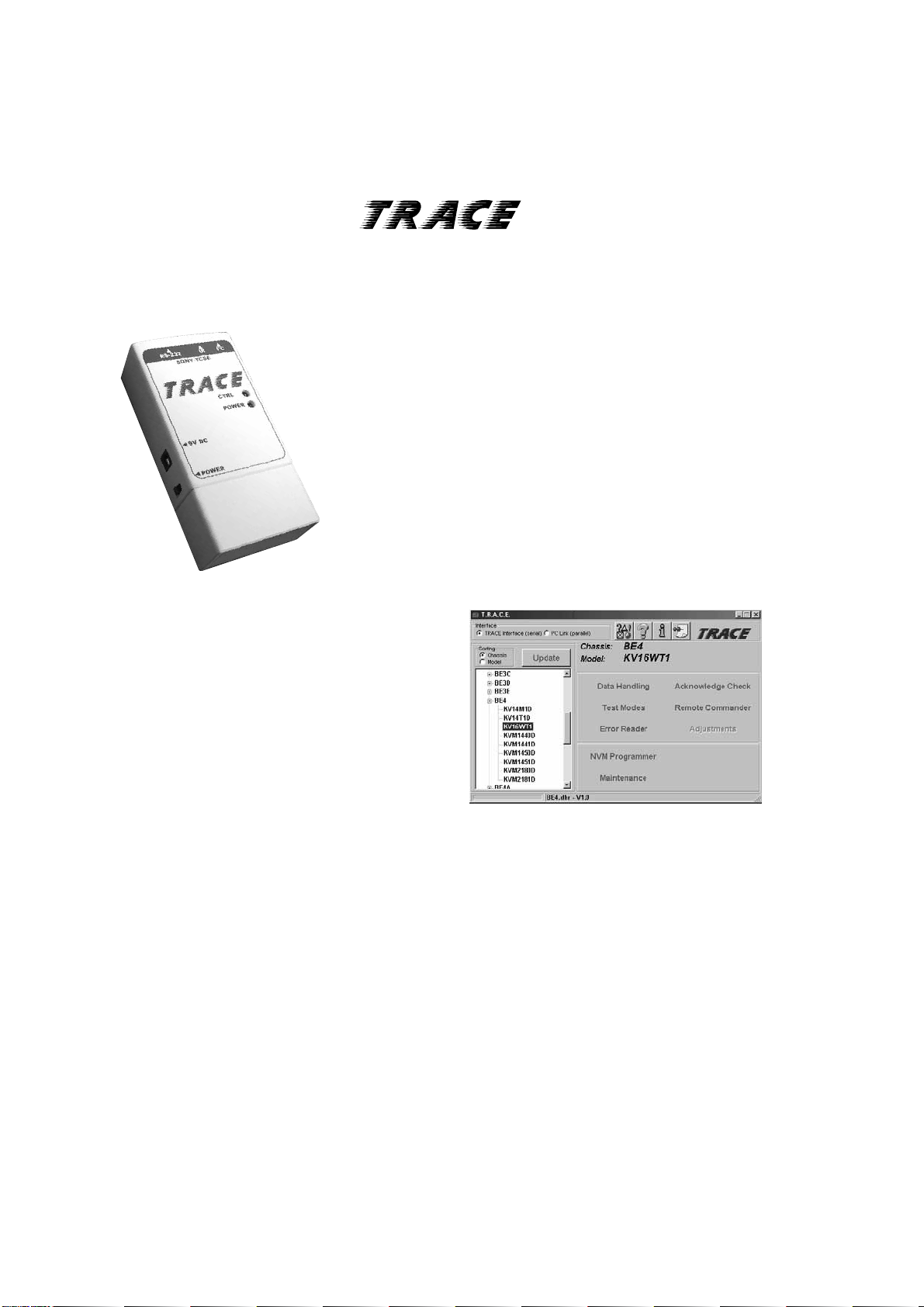
A new TV Repair Assistance Tool that combines ease of use and powerful PC software tools to
allow you to save valuable time during many TV repairs.
The TRACE interface connects to the PC's serial port. It provides
connection to the TV's I2C bus and can be provided with an InfraRed
transmitter (optional).
The interface is powered by a standard 9V PP3 battery for portable
use, and can also be powered by an external 9V/25mA DC power
supply.
The TRACE software that is supplied with the interface allows you to:
•
Read, restore and compare NVM contents via the I2C bus
Acknowledge check of all I2C devices in the TV set
•
Read Error Codes (emulation of the Error Reader tool)
•
With the optional IRAdd-on kit, the following features can be added:
Remote Commander emulation
•
User programmable Functional Check through Infrared
•
Fast and documented Test Mode setting of all SonyTV chassis
•
Additional features such as Adjustments and Troubleshooting are
available in chassis-dependent software modules. Please contact your
local Sony Service organisation for the latest information.
Note: For workshops already using the existing I2C Link parallel port interface (9-948-320-30), this software can be used as well, replacing the
TV Data Handling software (9-948-340-50), but Error Reader and IR functions can only be accessed with the TRACE interface.
Partnumbers: TRACE Starter Kit (TRACE interface + software): 9-948-320-70
TRACE Software (for users of the I2C Link interface): 9-948-340-80
TRACE IRAdd-on (IR interface + Remote Commander software): 9-948-320-80
PC requirements: IBM-compatible PC with operating system Windows95, Windows98, or WindowsNT*.
* WindowsNT only supported withTRACE interface
Sony Corporation
Sony UK
9-927-474-01
Service Promotions Dept.
English
04DP7100-1
Printed in U.K.
© 2004.04
 Loading...