Sony HXC-100 Service Manual

HD COLOR CAMERA
HXC-100
SERVICE MANUAL
Volume 1 1st Edition

!警告
このマニュアルは,サービス専用です。
お客様が,このマニュアルに記載された設置や保守,点検,修理などを行うと感電や火災,
人身事故につながることがあります。
危険をさけるため,サービストレーニングを受けた技術者のみご使用ください。
! WARNING
This manual is intended for qualifi ed service personnel only.
To reduce the risk of electric shock, fi re or injury, do not perform any servicing other than that
contained in the operating instructions unless you are qualifi ed to do so. Refer all servicing to
qualifi ed service personnel.
! WARNUNG
Die Anleitung ist nur für qualifi ziertes Fachpersonal bestimmt.
Alle Wartungsarbeiten dürfen nur von qualifi ziertem Fachpersonal ausgeführt werden. Um die
Gefahr eines elektrischen Schlages, Feuergefahr und Verletzungen zu vermeiden, sind bei
Wartungsarbeiten strikt die Angaben in der Anleitung zu befolgen. Andere als die angegeben
Wartungsarbeiten dürfen nur von Personen ausgeführt werden, die eine spezielle Befähigung
dazu besitzen.
! AVERTISSEMENT
Ce manual est destiné uniquement aux personnes compétentes en charge de l’entretien. Afi n
de réduire les risques de décharge électrique, d’incendie ou de blessure n’effectuer que les
réparations indiquées dans le mode d’emploi à moins d’être qualifi é pour en effectuer d’autres.
Pour toute réparation faire appel à une personne compétente uniquement.
HXC-100/V1 (E)

注意
ADVARSEL!
指定以外の電池に交換すると,破裂する危険があり
ます。
使用済の電池は,説明書に従って処理してください。
CAUTION
Danger of explosion if battery is incorrectly replaced.
Replace only with the same or equivalent type
recommended by the manufacturer.
Dispose of used batteries according to the
manufacturer’s instructions.
Vorsicht!
Explosionsgefahr bei unsachgemäßem Austausch
der Batterie.
Ersatz nur durch denselben oder einen vom
Hersteller empfohlenen ähnlichen Typ. Entsorgung
gebrauchter Batterien nach Angaben des
Herstellers.
Lithiumbatteri-Eksplosionsfare ved fejlagtig
håndtering.
Udskiftning må kun ske med batteri
af samme fabrikat og type.
Levér det brugte batteri tilbage til leverandøren.
ADVARSEL
Lithiumbatteri - Eksplosjonsfare.
Ved utskifting benyttes kun batteri som
anbefalt av apparatfabrikanten.
Brukt batteri returneres
apparatleverandøren.
VARNING
Explosionsfara vid felaktigt batteribyte.
Använd samma batterityp eller en likvärdig typ
som rekommenderas av apparattillverkaren.
Kassera använt batteri enligt gällande
föreskrifter.
ATTENTION
Il y a danger d’explosion s’il y a remplacement
incorrect de la batterie.
Remplacer uniquement avec une batterie du même
type ou d’un type équivalent recommandé par le
constructeur.
Mettre au rebut les batteries usagées conformément
aux instructions du fabricant.
VAROITUS
Paristo voi räjähtää jos se on virheellisesti
asennettu.
Vaihda paristo ainoastaan laitevalmistajan
suosittelemaan tyyppiin.
Hävitä käytetty paristo valmistajan ohjeiden
mukaisesti.
HXC-100/V1 (E)
1 (P)


Table of Contents
Manual Structure
Purpose of this manual .................................................................. 3
Related manuals ............................................................................ 3
Trademarks .................................................................................... 3
1. Service Overview
1-1. Connectors and Cables .................................................... 1-1
1-1-1. Connector Input/Output Signals ............................1-1
1-1-2. Wiring Diagrams for Cables .................................. 1-7
1-1-3. Connection Connectors/Cables .............................. 1-7
1-2. Location of Printed Circuit Boards .................................1-8
1-3. Circuit Description ........................................................ 1-10
1-4. Opening/Closing the Side Panel .................................... 1-16
1-5. Description of Onboard LED Indicators .......................1-17
1-6. Switch Settings ..............................................................1-20
1-7. Notes on Flexible Card Wire ......................................... 1-22
1-7-1. Disconnecting/Connecting Flexible Card Wire ... 1-22
1-7-2. Forming Flexible Card Wire ................................ 1-24
1-8. Notes on Replacement of Circuit Board .......................1-25
1-8-1. EEPROM Data .....................................................1-25
1-8-2. Actions to Be Taken during Board Replacement
and after Board Replacement/Repair ................... 1-25
1-8-3. Adjustment and Settings when Replacing SY-363
Board .................................................................... 1-26
1-9. Setting Intercoms........................................................... 1-27
1-10. Upgrading the Software Programs ................................ 1-28
1-10-1. Upgrading the Main Program .............................. 1-28
1-10-2. Upgrading the Boot Program ............................... 1-29
1-11. Note on Replacement of Lithium Battery ..................... 1-30
1-12. Periodic Check and Maintenance .................................. 1-31
1-12-1. Recommended Replacement Parts....................... 1-31
1-12-2. Periodic Replacement Parts ................................. 1-32
1-12-3. Cleaning the Air Vents .........................................1-32
1-13. Description of CCD Block Number .............................. 1-32
1-14. Optional Fixtures ........................................................... 1-33
1-15. Notes on Repair Parts .................................................... 1-33
1-16. Unleaded Solder ............................................................ 1-33
1-17. Installing the Accessory Shoe ....................................... 1-34
2. Replacement of Main Parts
2-1. Replacing the CCD Unit .................................................2-1
2-2. Replacing CCD Unit Boards ........................................... 2-3
2-2-1. DR-632 Board ........................................................ 2-3
2-2-2. NR-80 Board .......................................................... 2-3
2-2-3. PA-353 Board......................................................... 2-4
2-2-4. TG-265 Board ........................................................ 2-5
2-2-5. SE-949 Board .........................................................2-5
2-3. Replacing the DC Fan ..................................................... 2-6
2-4. Replacing Operation Parts ............................................... 2-7
2-5. Replacing Connectors .....................................................2-8
2-5-1. CCU (TRIAX) Connector ...................................... 2-8
2-5-2. SDI Connector .....................................................2-10
2-6. Replacing the Power Supply Assembly ........................ 2-11
2-7. Removing/Installing the Connector Panel..................... 2-12
2-8. Replacing Boards .......................................................... 2-13
2-8-1. CD-61 Board ........................................................ 2-13
2-8-2. CN-3069 Board .................................................... 2-14
2-8-3. CN-3070 Board .................................................... 2-15
2-8-4. CN-3071 Board .................................................... 2-15
2-8-5. CN-3072 Board .................................................... 2-16
2-8-6. DPR-298 Board ...................................................2-17
2-8-7. ENC-112 Board ...................................................2-17
2-8-8. FL-348 Board .......................................................2-18
2-8-9. LE-355 Board ......................................................2-19
2-8-10. MB-1125 Board ................................................... 2-19
2-8-11. MS-91 Board ....................................................... 2-20
2-8-12. PS-755 Board ....................................................... 2-20
2-8-13. RE-263 Board ...................................................... 2-20
2-8-14. SW-1404 Board.................................................... 2-21
2-8-15. SW-1405 Board.................................................... 2-21
2-8-16. SW-1406/A Board ................................................ 2-22
2-8-17. SW-1407 Board.................................................... 2-22
2-8-18. SY-363 Board ....................................................... 2-23
2-8-19. TX-126 Board ...................................................... 2-23
HXC-100/V1 (E)
1

3. Electrical Alignment
4. File System
3-1. Preparations ..................................................................... 3-1
3-1-1. Equipment Required .............................................. 3-1
3-1-2. Precautions on Adjustments ................................... 3-1
3-1-3. File Data at Adjustment ......................................... 3-2
3-1-4. Maintaining the Grayscale Chart ........................... 3-2
3-1-5. Setup Menu ............................................................ 3-4
3-1-6. Connection of Equipment ...................................... 3-5
3-1-7. Initial Settings ........................................................ 3-6
3-1-8. Adjustment Items and Setup Menu Items .............. 3-7
3-2. Automatic Adjustment..................................................... 3-8
3-3. Electrical Alignment ........................................................3-8
3-3-1. BLACK SET Adjustment ...................................... 3-8
3-3-2. Sensitivity Adjustment ........................................... 3-9
3-3-3. V-SUB Adjustment .............................................. 3-10
3-3-4. Black Shading Adjustment................................... 3-11
3-3-5. White Shading Adjustment .................................. 3-12
3-3-6. RPN Adjustment .................................................. 3-14
3-4. Video System Level Adjustment ................................... 3-15
3-4-1. H/V Ratio Adjustment ......................................... 3-15
3-4-2. Detail Level Adjustment ...................................... 3-16
3-4-3. Crispening Adjustment ........................................ 3-17
3-4-4. Level Dependent Adjustment............................... 3-18
3-4-5. Detail Clip Adjustment ........................................ 3-19
3-4-6. Auto-iris Adjustment ........................................... 3-20
3-4-7. Pedestal Level Adjustment................................... 3-21
3-4-8. Flare Adjustment .................................................. 3-22
3-4-9. Gamma Correction Adjustment ........................... 3-23
3-4-10. Knee Point/Knee Slope Adjustment .................... 3-24
3-4-11. White Clip Level Adjustment .............................. 3-25
3-4-12. File Store ..............................................................3-25
3-5. ND Offset Adjustment ...................................................3-26
3-6. RPN Compensation .......................................................3-27
3-6-1. Automatic Compensation (APR) ......................... 3-27
3-6-2. Manual RPN Compensation Adjustment ............. 3-27
3-6-3. Procedures to Be Taken When the RPN
Compensation Fails .............................................3-29
3-6-4. Performing Automatic RPN Detection
Effectively ............................................................ 3-30
3-6-5. RPN Compensation Flowchart ............................ 3-31
3-7. Vertical Line Compensation .......................................... 3-32
3-8. TRIAX Transmission System Adjustment .................... 3-34
3-8-1. 1.4-MHz Modulation Circuit Adjustment ............3-34
3-8-2. Demodulation Circuit Adjustment .......................3-35
3-9. TEST OUT Output Level Adjustment........................... 3-36
4-1. File Structure ...................................................................4-1
4-2. Operator File ...................................................................4-2
4-3. Preset Operator File ......................................................... 4-3
4-4. Scene File ........................................................................ 4-4
4-5. Reference File .................................................................4-6
4-6. Lens File .......................................................................... 4-8
4-7. OHB File ....................................................................... 4-10
4-8. File Items ....................................................................... 4-12
5. Setup Menu
5-1. Entering the SERVICE Menu ......................................... 5-1
5-2. Settable Special Functions ..............................................5-1
5-3. Description on SERVICE Menu ..................................... 5-2
2
HXC-100/V1 (E)

Purpose of this manual
Related manuals
Manual Structure
This manual is the service manual Volume 1 for HD Color Camera HXC-100.
This manual describes the information items that premise the service based on the
components parts such as service overview, replacement of main parts, electrical
alignment, fi le system, SERVICE menu, assuming use of system and service engi-
neers.
Besides this service manual Volume 1 the following manual is available for this unit.
. HXC-100 Operating Instructions (Supplied with HXC-100)
This manual is necessary for application and operation of HXC-100.
Part number: 4-137-704-0X (Japanese)
Part number: 4-137-704-1X (English)
. HXC-100 Operating Instructions CD-ROM (Supplied with UC and CE
model)
This manual is necessary for application and operation of HXC-100.
The CD-ROM contains the English, French, German, Italian, and Spanish operating
instructions (PDF).
Part number: 4-137-707-0X
Trademarks
. Service Manual Volume 2 (Available on request)
Describes the parts list, block diagrams, schematic diagrams and board layouts of
HXC-100.
. “Semiconductor Pin Assignments” CD-ROM (Available on request)
This “Semiconductor Pin Assignments” CD-ROM allows you to search for semiconductors used in Broadcast and Professional equipment.
The service manual Volume 2 contains a complete list of semiconductors and their
ID Nos., and thus should be used together with the CD-ROM.
Part number: 9-968-546-06
Trademarks and registered trademarks used in this manual are follows.
. FRAM is a registered trademark of Ramtron International Corporation.
HXC-100/V1 (E)
3

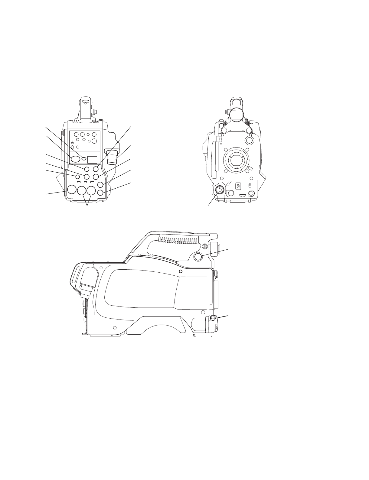
Service Overview
1-1. Connectors and Cables
1-1-1. Connector Input/Output Signals
Section 1
5
6
8
9
0
!-
!=
7
1
2
3
4
![
!]
Input/Output Signals
1 CCU (TRIAX) connector
J: TAGIMI Triax connector
UC: LEMO Triax connector
CE: Fischer Triax connector
2 PROMPTER/GENLOCK/RET
BNC type 75 Z, 1.0 V p-p
3 TEST OUT
BNC type 75 Z, 1.0 V p-p
HXC-100/V1 (E)
!\
Output Signals
4 SDI
HD SDI signal
BTA-S004A compliant
BNC type 75 Z, 0.8 V p-p 1.485 Gbps
5 EARPHONE
EARPHONE φ3.5 mm stereo mini jack
1-1

6 INTERCOM (5P FEMALE)
(External view)
No. Signal I/O Specifi cations
1 Intercom MIC (Y) IN CARBON (_20 dBu, Unbalance)
2 Intercom MIC (X) IN
3 GND
_
DYNAMIC (_60 dBu, Balance/Unbalance)
MANUAL (_20/_40/_60 dBu, Balance/Unbalance)
GND
4 Intercom Left OUT 11 dBu (VR Max, 250 Z Load)
5 Intercom Right OUT 11 dBu (VR Max, 250 Z Load)
7 REMOTE (8P FEMALE)
1
7
2
8
3
6
5
4
(0 dBu = 0.775 Vrms)
(External view)
No. Signal I/O Specifi cations
for RCP for TRUNK (RS-422A)
1 TX (X) TX1 (+) OUT SERIAL DATA OUT/TRUNK DATA OUT
2 TX (Y) TX1 (_) OUT
3 RX (X) RX1 (+) IN SERIAL DATA IN/TRUNK DATA IN
4 RX (Y) RX1 (_)IN
5 TX-GND
_
6 UNREG-OUT OUT
7 UNREG-GND
_
GND for TX
+10.5 to +17 V dc, 200 mA (max)
GND for UNREG-OUT
8 RCP-PIX OUT 75 Z, 1.0 V p-p (SD Video)
CHASSIS GND
_
CHASSIS GND
1-2
HXC-100/V1 (E)

8 RET CTRL (6P FEMALE)
(External view)
No. Signal I/O Specifi cations
1 INCOM MIC-ON/OFF (J, UC)
IN Zi > 10 kZ, ON : GND, OFF : OPEN
ENG (CE)
2 NC (J, UC) No connection
PROD (CE) IN Zi > 10 kZ, ON : GND, OFF : OPEN
3 GND
_
4 RET 3-ON/OFF IN Zi > 10 kZ, ON : GND, OFF : OPEN
5 RET 1-ON/OFF IN Zi > 10 kZ, ON : GND, OFF : OPEN
6 RET 2-ON/OFF IN Zi > 10 kZ, ON : GND, OFF : OPEN
9 TRACKER (10P FEMALE)
81
27
10 9
63
54
(External view)
No. Signal I/O Specifi cations
1 TRACKER LEFT OUT TRACKER Output, _20 dBu unbalance
2 GND (TALK)
3 GND (RECEIVE/PGM/TALLY)
_
_
GND for TRACKER TALK
GND for RECEIVE/PGM/TALLY
4 TRACKER RIGHT OUT TRACKER Output, _20 dBu unbalance
5 UNREG OUT
6 GND (UNREG)
_
+10.5 to 17 V dc
GND for UNREG
7 TRACKER TALK (X) IN TRACKER TALK
8 TRACKER TALK (Y) IN
0 dBu /_20 dBu, High impedance balanced
9 G TALLY OUT ON : GND
OFF : High impedance (Open collector)
10 R TALLY OUT ON : GND
OFF : High impedance (Open collector)
(0 dBu = 0.775 Vrms)
HXC-100/V1 (E)
1-3

0 DC OUT (4P FEMALE)
1
4
23
(External view)
No. Signal I/O Specifi cations
1 UNREG GND
2 NC No connection
3 NC No connection
4 UNREG-OUT OUT
_
GND for UNREG-OUT
+10.5 to 17 V dc, 500 mA (max)
!- DC IN (4P MALE)
(External view)
No. Signal I/O Specifi cations
1 EXT_DC (C)
2 NC No connection
3 NC No connection
4 EXT_DC (H) IN
AUDIO IN CH1/CH2 (3P FEMALE)
!=
No. Signal I/O Specifi cations
1 AUDIO CH1/CH2 (G)
2 AUDIO CH1/CH2 (X) IN
3 AUDIO CH1/CH2 (Y) IN
_
21
(External view)
__60 dBu, _50 dBu, _40 dBu, _30 dBu, _20 dBu,
GND for DC (+)
+10.5 to 17 V dc
3
LINE (0 dBu) selectable, Balanced
(0 dBu = 0.775 Vrms)
1-4
HXC-100/V1 (E)

![ FRONT MIC (3P FEMALE)
21
3
(External view)
No. Signal I/O Specifi cations
1 MIC 1 (G)
2 MIC 1 (X) IN
3 MIC 1 (Y) IN
__60 dBu, _50 dBu, _40 dBu, _30 dBu, _20 dBu,
selectable, Balanced
!] VF (20P FEMALE)
(External view)
(0 dBu = 0.755 Vrms)
No. Signal I/O Specifi cations
1 S-DATA IN/OUT TTL level
2 NC No connection
3 NC No connection
4 SCK OUT TTL level
5 NC No connection
6 NC No connection
7 NC No connection
8 G TALLY OUT ON : 5 V, OFF : GND
9 NC No connection
10 NC No connection
11 NC No connection
12 Y VIDEO OUT 1.0 V p-p, Zo = 75 Z
13 VIDEO GND
14 Pb VIDEO OUT
15 Pr VIDEO OUT
16 NC No connection
17 R TALLY OUT ON : 5 V, OFF : GND
18 NC No connection
19 UNREG GND
20 UNREG OUT
_
_
GND for VIDEO
?0.35 V p-p, Zo = 75 Z
?0.35 V p-p, Zo = 75 Z
GND for UNREG
+10.5 to +17 V
HXC-100/V1 (E)
1-5
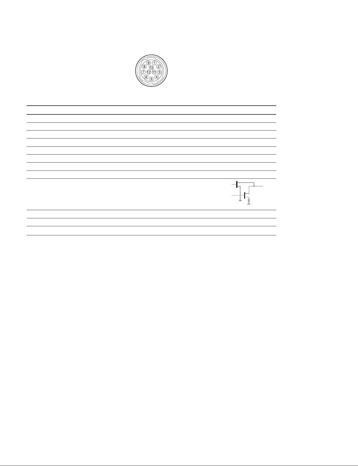
!\ LENS (12P FEMALE)
(External view)
No. Signal I/O Specifi cations
1 RET VIDEO ENABLE IN ENABLE : 0 V, DISABLE : +5 V or OPEN
2 VTR START/STOP IN ENABLE : 0 V, DISABLE : +5 V or OPEN
3 GND
4 SERVO MA/AT OUT AUTO : +5 V, MANU : 0 V or OPEN
5 IRIS POSITION OUT
6 UNREG OUT
7 IRIS POSITION IN
8 IRIS AT/MA OUT AUTO IRIS : 0 V, MANUAL IRIS : +5 V
9 EXTENDER ON/OFF IN EX 2 ON : GND
10 ZOOM POSITION IN WIDE : 2 V, TELE : 7 V
11 FOCUS POSI (/LENS RX) IN
12 (LENS TX) OUT
_
GND for UNREG
+3.4 V (F16) to +6.2 V (F2.8)
+10.5 to +17 V
+3.4 V (F16) to +6.2 V (F2.8)
EX 0.8 ON : 30 kZ to GND
OFF : OPEN
% : 7 V, min. : 2 V
EX 2 ON
EX 0.8 ON
30 k7
1-6
HXC-100/V1 (E)
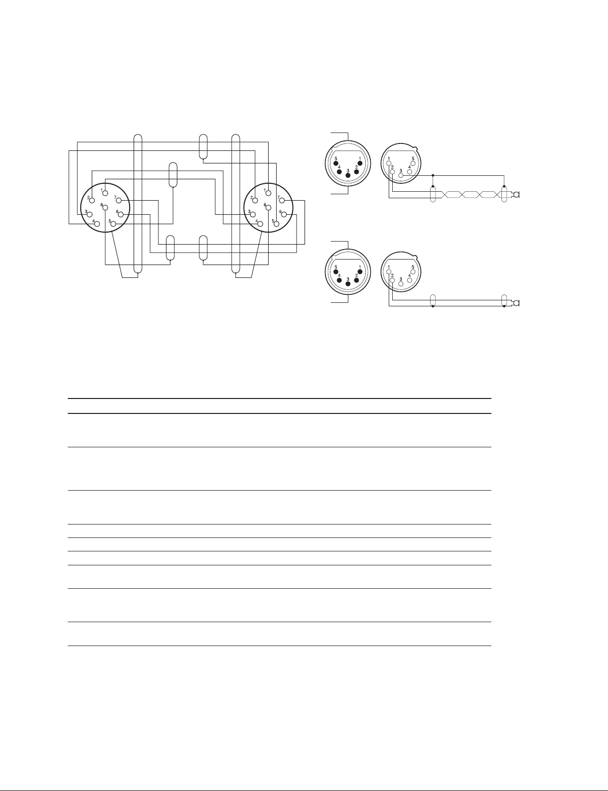
1-1-2. Wiring Diagrams for Cables
CCA-5 Cable
INTERCOM MIC Cable
(1) Balance (HEAD SET menu UNBAL: OFF)
Black
White
Orange
White
Brown
Red
G
X
Y
(2) Unbalance (HEAD SET menu UNBAL: ON)
White
Red
BrownBrown
— 8P CONNECTOR (MALE) —
(WIRING SIDE)
X
Y
1-1-3. Connection Connectors/Cables
Connection made with the connector panels during installation or service, should be made with the connectors/complete cable assemblies specifi ed in the following list, or equivalent parts.
INTERCOM
MIC
INTERCOM
MIC
Connector Name Connector/Cable
CCU (TRIAX) Fujikura φ8.5 mm
Fujikura φ14.5 mm
Belden 9232 φ13.2 mm
TEST OUT
1-569-370-12 Plug, BNC
PROMPTER/GENLOCK/RET
SDI
(BNC)
AUDIO IN CH1/CH2
1-508-084-00 XLR, 3P Male or ITT Cannon XLR-3-12C equivalent
MIC
(3P FEMALE)
RET CONTROL (6P FEMALE) 1-560-078-00 Plug, 6P Male or HIROSE HR10-7PA-6P equivalent
DC OUT (4P FEMALE) 1-566-425-11 Plug, 4P Male or HIROSE HR10A-7P-4P equivalent
INTERCOM (5P FEMALE) 1-508-370-11 XLR, 5P Male or ITT Cannon XLR-5-12C equivalent
DC IN (4P MALE) 1-508-362-00 XLR, 4P Female or ITT Cannon XLR-4-11C equivalent
DC cable CCDD-X2 (2 m)
REMOTE (8P FEMALE)
. 1-766-848-11 Plug, 8P Male or CCA-5 cable assembly
(CCA-5-10 (10 m)/CCA-5-3 (3 m)) (optional)
*2 *3
. REMOTE cable 1-783-372-11 (supplied with RM-B150, 10 m)
*1 *2 *3
TRACKER (10P FEMALE) 1-506-522-12 Connector, Round Type 10P
or HIROSE HR10A-10P-10P equivalent
*1: Use of REMOTE cable enables to monitor video signals. (The pin 8 is available for the video signal line.)
The down-converted SD signal is output.
*2: If you want to use a cable of length different from a standard product, contact your local Sony Sales Offi ce/Service Center.
n
*3: The pin 8 of CCA-5 cable is GND (ground).
The pin 8 of REMOTE cable is not GND (ground).
HXC-100/V1 (E)
1-7
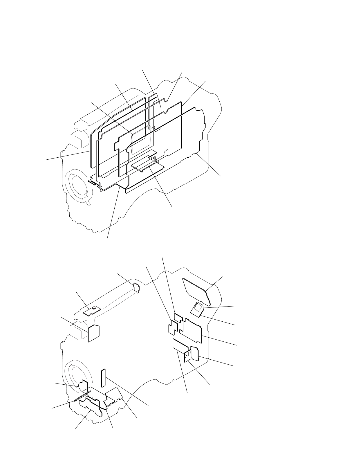
1-2. Location of Printed Circuit Boards
TX-126
ENC-112
CD-61
FL-348
DPR-298
PS-755
SY-363
RE-263
CN-3069
CN-3701
CN-3070
SW-1403
MB-1125
LE-355
CN-3074
CN-3075
SW-1406 (J, UC)
SW-1406A (CE)
CN-3073
CN-3072
CN-3076
CN-3078
SW-1407
CN-3077
SW-1402
1-8
SW-1405
SW-1404
MS-91
HXC-100/V1 (E)
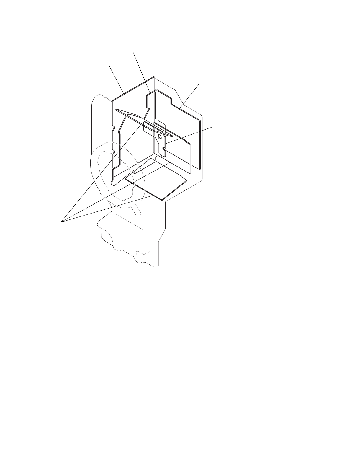
TG-265
DR-632
NR-80
SE-949
PA-353
HXC-100/V1 (E)
1-9

1-3. Circuit Description
Optical System Block (CCD Unit)
PA-353 Board
This board, consisting of a CCD drive H driver and a sample-hold IC, performs correlated double sampling for signals from the CCD and outputs them differentially. The sample-hold IC adjusts sensitivity.
DR-632 Board
This board consists of a CCD V driver circuit and a buffer for CCD and sample-hold IC drive pulses.
TG-265 Board
This board consists of the following circuits.
. A PLD that generates CCD and sample-hold IC drive pulses and a video amplifi er
. A circuit to lock (using PLL) and synchronize the INT PLL H signal generated by the PLD with the
PLL H X and PLL H Y signals sent from the DPR-298 board
The master gain is switched with the step gain in the video amplifi er.
NR-80 Board
This board performs CCD defect correction and black shading, etc.
SE-949 Board
This board detects the ND fi lter disk position.
Signal Processing Block
DPR-298 Board
This board performs main camera signal processing for video signals.
Video signals are digitized by the video amplifi er and the A/D converter, and are transferred to the main
process IC (IC401) through the pre-process PLDs (IC301 to 303) for video signal processing.
The sub-process IC (IC501) and the PLD (IC701) perform video processing for the external interface.
This board also contains a serial digital signal converter IC, an analog video D/A converter, and a reference clock signal generator.
CD-61 Board
This board encodes the main-line signal and decodes the return signal and the prompter signal.
Main-Line Signal
The main-line signal processed on the DPR-298 board is encoded by the encoder and is transferred to the
OFDM modulation IC. This IC multiplexes the main-line signal and the audio signal and a command sent
from the SY-363 board to a 2-channel signal, D/A-converts the 2-channel signal, and then sends it to the
TX-126 board.
Return Signal
This board receives the OFDM-demodulated stream signal from the TX-126 board, and divides it into a
return video signal, prompter signal, audio signal for intercom, and a command signal.
The return video signal is decoded to a baseband signal by the decoder, and is then sent to the DPR-298
board.
The audio signal and the command are sent to the SY-363 board.
1-10
HXC-100/V1 (E)

Prompter Signal
This signal is sent to the MPEG2 decoder on the ENC-112 board for decoding.
In the case of the VBS prompter, the decoded signal is output from the VBS encoder (IC1201) on the
CD-61 board to the SY-363 board.
In the case of the HD prompter, the decoded signal is sent to the DPR-298 board.
ENC-112 Board
This small board is mounted on the CD-61 board, and compresses/decompresses the video signal for
prompter.
IC100 functions for MPEG2 encoding and decoding, but is used only for decoding in this unit.
Signal Transmission Block
TX-126 Board
This board consists of a OFDM signal transmitter/receiver circuit for transmission of the video signal,
audio signal, intercom signal, and commands, and an FM modulation/demodulation circuit for transmission of the standby intercom signal, synchronizing signal, and TONE signal.
OFDM Signal Transmitter/Receiver Circuit
The OFDM signal output consists of six waves F1 to F6 to transmit video, sub video, microphone, intercom, and command signals.
The OFDM signal transmitter, consisting of two systems: LOW band (F1 to F3) and MID band (F4 to F6),
amplifi es the OFDM signal generated by the D/A converter on the CD-61 board independently for each
band. The LOW band signal is mixed with the 1.4 MHz FM-modulated signal and is combined with the
MID band signal in the MPX fi lter (FL601), and then the composite signal is output to the CCU.
The OFDM signal input consists of three waves F7 to F9 to transmit return video, prompter video, intercom, PGM, and command signals.
The OFDM signal receiver that is composed independently for F7 to F9 amplifi es the waves F7 to F9
output from the HPF of the MPX fi lter (FL601), selects them by band with the BPF (FL301, FL401, and
FL501), and then processes them.
The level of each signal selected by band is regulated by the step gain amplifi er that automatically switch-
es amplifi er gain to four steps according to the input level and by the AGC amplifi er (IC302, IC402, and
IC502), and then the center frequency of F7 to F9 is converted to 36 MHz by the MIXER IC (IC303,
IC403, and IC503). The converted OFDM signal is converted to TS data by the demodulator ICs (IC603,
IC604, and IC605), and then the serial data is output to the CD-61 board.
FM Modulation and Demodulation Circuits
The FM modulation circuit mixes the standby INCOM signal (STB INCOM TO CCU: CHU → CCU)
and the TONE signal (16.38 kHz), modulates (FM) the mixed signal with a carrier frequency of 1.4 MHz,
and then sends the signal to the CCU.
In the FM demodulation circuit, the FM signal (that is modulated with 1.0 MHz carrier frequency) is
extracted from the RF signal sent from the CCU by the MPX fi lter (FL601) and the BPF (FL2), and the
FM signal is demodulated to a standby INCOM signal (STB INCOM FR CCU: CCU → CHU) and a
synchronizing signal by the demodulator (IC13 LA2135M).
The demodulated standby INCOM signal is output by the output amplifi er at a signal level of 220 mVp-p
(0 dBu input). The synchronizing signal waveform is shaped, and the signal is output with an amplitude of
3.3 Vp-p.
The 1.0 MHz FM-modulated wave is detected by IC16 to check the presence of an FM signal wave.
HXC-100/V1 (E)
1-11

System Control Block
SY-363 Board
This board comprises a CPU, peripheral devices, interfaces, a sync separator circuit, a video amplifi er,
and a audio circuit.
CPU and Peripheral Devices
The CPU runs on the program stored in the fl ash memory (IC118, IC119).
The program can be upgraded with a Memory Stick through the Memory Stick controller (IC128).
The SY-363 board also comprises SRAM chips (IC122, IC123) and a FRAM chip (IC127) to record
system setup data and other data.
The CPU’s serial communication port is used to control the CCD block, and serial lens.
The analog input ports (AN0 to AN7) are used to read analog lens signals (Iris, Focus, Zoom, and Extender), temperatures of the CCD and boards, and audio volume.
The CPU’s external bus (IC109, IC114, and IC125) is used to control the video signal processing LSI and
PLD on the DPR-298 board and the communication LSI and PLD on the CD-61 board through the
MB-1125 board.
In addition to these, this board is provided with a calendar function RTC (IC108). BT101 and C118
function as the RTC backup power supply.
700 Protocol Communication
IC145 performs 700 protocol communication between the camera and the REMOTE connector of the
CCU. Data to be sent for communication with the CCU is multiplexed on the CD-61 board, and is then
sent to the CCU. The REMOTE connector is shared with TRUNK, which are switched by the AT-PLD.
AT-PLD (IC151)
The AT-PLD is a PLD to control external inputs/outputs and the internal devices of the unit. The AT-PLD
has the following functions.
. I2C communication and 3-wire serial communication with the CCD block
. I2C communication with the viewfi nder and tally output
. I2C communication with the front boards
. Inputs of rear panel switches, handle switch, and two rotary encoders
. Tally output to the handle and TRACKER connector
. D/A converter output for lens iris control
. CPU’s V interrupt control
. Communication with the character generator on the DPR-298 board
. Fan speed detection
. Monitoring PLD and power status on each board
1-12
HXC-100/V1 (E)

VDAP-PLD (IC655)
The VDAP-PLD adjusts the phases of the genlock timing generator, SD sync signal, and HD sync signal,
and controls the video selector, audio matrix processing, and the analog circuit (including the microphone
amplifi er).
. Video block
The video block has two functions: a sync separator circuit for genlock and a video amplifi er circuit for
the VF, TEST OUT, and PROMPTER connectors. The VF analog signal from the DPR-298 board
passes through the LPF and is output from the VF connector and the BUILD UP connector. The VBS
signal passes through the LPF and is output from the REMOTE connector (PIX output) and the TEST
OUT connector.
The SD sync and HD sync signals are phase-adjusted by the VDAP-PLD, and are then output from the
TEST OUT connector.
The same connector is used for prompter output and genlock input. When the CCU is connected, the
connector outputs the prompter signal from the CD-61 board. When the unit is standalone, the connector is used for genlock input, and the Reference-H, F signals are generated by the sync separator circuit
and are then sent to the DPR-298 board.
. Audio Processing Block
This block is provided with input/output amplifi ers and A/D and D/A converters for the microphone,
intercom, earphone, and TRACKER, and a digital matrix to add signals. This block also has a standby
intercom circuit for communication with the CCU in the standby state.
The FRONT MIC connector or AUDIO IN connector is selectable for the microphone input, and only
the AUDIO IN connector is compatible with the LINE-level input. The microphone input is provided
with variable gain that can be switched within a range of -60 dBu to -20 dBu in 10 dBu step and +48V
Phantom power supply. The microphone input is not compatible with AB POWER.
The intercom input is provided with gain switching (-20, -40, or -60 dBu) and power supply (approx. 10
V) for carbon microphone. The TRACKER input is provided with gain switching (0 or -20 dBu).
Each input passes through the pre-fi lter, is A/D-converted, and is then input to the VDAP-PLD.
The microphone and intercom outputs are switched and added by the VDAP-PLD, are multiplexed on
the CD-61 board, and are then output to the CCU. Signals from the CCU are transferred to the CD-61
board and then input to the VDAP-PLD that performs signal addition according to each output and
volume processing. Then the signals are output to the D/A converters for the intercom, earphone, and
TRACKER. The D/A converter output signals pass through the analog LPFs and the output drivers, and
are then output from each connector.
In the standby state, the standby audio input (STBY Incom in signal) from the TX-126 board is adjusted
for volume by the electronic potentiometer (IC603), and then becomes an intercom output. The mute
circuit (IC588 to IC591) prevents the Triax-H signal from becoming an intercom output.
MS-91 Board
This board contains a Memory Stick slot, an access indicator LED, and two I2C controllers for board
input/output at the front and inside.
LE-355 Board
This board contains handle tally LEDs (red, green ) and an ON/OFF switch.
CN-3069 Board
This board contains a VF connector.
CN-3070 Board
This board contains a LENS connector.
HXC-100/V1 (E)
1-13

CN-3071 Board
This board contains a FRONT MIC connector (XLR 3-pin, female).
CN-3072 Board
This board contains an INTERCOM connector (XLR 5-pin, female).
CN-3073 board
This board contains an EARPHONE connector (φ3.5 mm stereo mini jack).
CN-3074 Board
This board contains a REMOTE connector (round, 8-pin).
CN-3075 Board
This board contains a TEST OUT connector, PROMPTER/GENLOCK/RET connector, and two BNC
connectors.
CN-3076 Board
This board contains the following switches and connectors.
. AUDIO IN switching switch × 3
. RET CTRL connector (round, 6-pin)
. TRACKER connector (round, 10-pin)
. DC OUT connector (round, 4-pin)
CN-3077 Board
This board contains two AUDIO IN connectors (XLR 3-pin, female) on the connector panel.
CN-3078 Board
This board contains a DC IN connector (XLR 4-pin, male).
SW-1402 Board
This board contains two ASSINABLE switches on the inside panel.
SW-1403 Board
This board contains two handle switches (RET, INCOM).
SW-1404 Board
This board contains fi ve switches (GAIN, DCC, WHITE, MENU, and DISPLAY) on the inside panel.
SW-1405 Board
This board contains three switches on the front panel, a potentiometer, and a rotary encoder.
SW-1406/A Board
This board contains seven switches on the intercom panel, potentiometers (CE: 5 and UC: 3), and a rotary
encoder.
SW-1407 Board
This board contains a CAM POWER switch.
1-14
HXC-100/V1 (E)

Power Supply
PS-755 Board
Input power voltages include 38 Vdc to 180 Vdc supplied by the CCU and 10 Vdc to 17 Vdc supplied by
the external DC power supply unit.
Output power voltages are as follows:
. Standby voltages +13.5 V and _5.5 V
. Voltage 14 V for viewfi nder
. Voltage 14 V for lens
. Voltage 14 V for utility
. Voltage 48 V for audio circuit
. Voltage 26 V for intercom
. Voltages 6.5 V and 1.8 V for CCD
. Other voltages 5.5 V, 3.8 V, and _5.5V
When 38 V is supplied from the CCU, only standby voltages +13.5 V and _5.5 V are output. When 180 V
is supplied from the CCU, all voltages are output. When voltages are supplied by the external DC power
supply unit, all voltages are output.
RE-263 Board
This small board on the PS-755 board outputs voltages 25 V, 15.5 V, and _8.5 V for the CCD.
MB-1125 Board
This is the motherboard of the unit, which contains interface with each board, inductors for power fi lters
of each board, capacitors, a positive-characteristic thermistor to prevent overcurrent, and a fuse.
FL-348 Board
This board isolates RF signals from the DC power for this unit.
HXC-100/V1 (E)
1-15
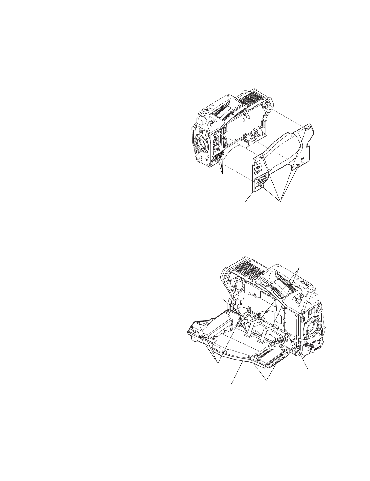
1-4. Opening/Closing the Side Panel
Inside Panel
1. Loosen the four screws with stopper to detach the
inside panel.
2. Reinstall the inside panel by reversing the step above.
n
Turn all the toggle switches to the front side, and then
attach the inside panel.
Toggle switches
Inside panel
Screws with stopper
Outside Panel
1. Loosen the fi ve screws with stopper and open the
outside panel in the arrow direction.
2. Hook the outside panel to potion A (two locations) to
fi x it.
n
Be careful so that the fl exible card wires between the
TX-126 and CD-61 boards do not shift or come off.
3. Close the outside panel by reversing the steps above.
A
Screws with stopper
Outside panel
Flexible card wires
A
Screws with stopper
1-16
HXC-100/V1 (E)

1-5. Description of Onboard LED Indicators
CD-61 Board
AB C DE
D1
1
2
3
4
CD-61 BOARD (SIDE A)
Ref No. Name Color Description Normal state
D1 PWR Green Lights when all power voltages are nor-
mal when the CCU is connected.
Lit
DPR-298 Board
DCBAE
1
2
3
4
D401
DPR-298 BOARD (SIDE B)
Ref No. Name Color Description Normal state
D101 POWER Green Lights when all power voltages on the
D401 CTL Green Lights instantly at power-on and is
D101
Lit
board are normal.
_
turned off immediately by the CPU
control.
HXC-100/V1 (E)
1-17

ENC-112 Board
BA
D100
D101
D102
1
2
ENC-112 BOARD (SIDE B)
Ref No. Name Color Description Normal state
D100 STATUS 0 Green Blinks while IC100 on the ENC-112
D101 STATUS 1 Green
board is functioning.
Blinking
D102 STATUS 2 Green
SY-363 Board
BCDE A
1
D535
D10 D11
2
D201
3
SY-363 BOARD (SIDE B)
Ref No. Name Color Description Normal state
D10 CAM-PW Green Lights while the main power is sup-
plied.
CCU connected
ON: Lit
Standby: Off
D11 STBY-PW Green Lights while the standby power is
Lit
supplied.
D201 Status Green Not used
D535 RTS PW Red While the INTERCOM connector is
_
Off
supplied with RTS PW (+26 V).
1-18
HXC-100/V1 (E)

TX-126 Board
B
A
1
2
3
4
GFEDC
D205
TX-126 BOARD (SIDE A)
Ref No. Name Color Description Normal state
D205 POWER Green Lights while both main power and
standby power are supplied.
CCU connected
ON: Lit
Standby: Off
CCU disconnected: Off
HXC-100/V1 (E)
1-19

1-6. Switch Settings
n
Do not change the settings of unused switches.
CD-61 Board
AB C DE
1
2
S701
3
4
CD-61 BOARD (SIDE A)
Ref No. Bit Description Factory setting
S701 1 Not used OFF
2 Not used OFF
3 Not used OFF
4 OFF: Normal operation (for upgrading the PLD from the SY-363 board)
OFF
ON: For upgrading the PLD from CN701 on the CD-61 board
DPR-298 Board
BCDEA
1
2
3
S901
4
DPR-298 BOARD (SIDE A)
Ref No. Bit Description Factory setting
S901 1 Not used OFF
2 Not used OFF
3 Not used OFF
4 OFF: Normal operation (for upgrading the PLD from the SY-363 board)
OFF
ON: For upgrading the PLD from CN901 on the DPR-298 board
1-20
HXC-100/V1 (E)

SY-363 Board
BCDE A
1
S502
2
S101
S201
3
SY-363 BOARD (SIDE B)
Ref No. Bit Description Factory setting
S101 1 OFF: Normal operation
ON: Forcible fi rmware upgrade
2 Not used OFF
3 OFF: Normal operation
ON: FRAM clear
4 Not used OFF
S201
(MODE)
1 Not used OFF
2 Not used OFF
3 Not used OFF
4 Not used OFF
S502
_
Intercom output interface switching
Normal: 4-wire
RTS: RTS/Clear-Com
OFF
OFF
OFF
HXC-100/V1 (E)
1-21
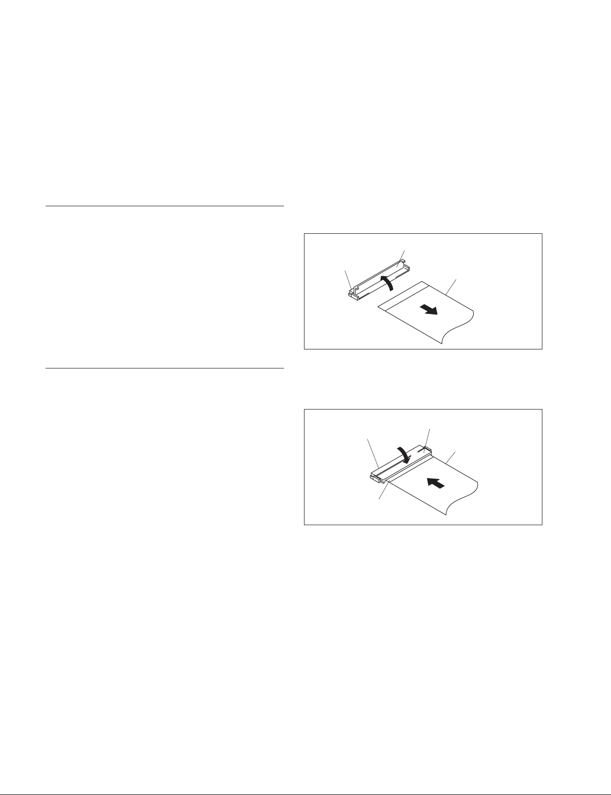
1-7. Notes on Flexible Card Wire
1-7-1. Disconnecting/Connecting Flexible Card Wire
Flexible card wires are used between the boards of this unit. Take care not to bend forcedly these fl exible
card wires. This shortens the wire life.
Type-A
Disconnecting
1. Raise the connector open/close lever in the arrow A
direction to unlock the coupling.
2. Pull out the fl exible card wire in the arrow B direction.
Connecting
m
. Be careful not to insert the fl exible card wire obliquely.
. Check that the conducive surface of the fl exible card
wire is not contaminated.
1. Insert the fl exible card wire in the arrow A direction as
far as it will go with the insulating surface facing
upward.
2. Close the connector open/close lever in the arrow B
direction to lock the fl exible card wire.
Connector
Connector
Insulating surface
Connector open/close lever
Flexible card wire
A
B
Connector open/close lever
Flexible card wire
B
A
1-22
HXC-100/V1 (E)
 Loading...