

Page 1

HD ELECTRONIC VIEWFINDER
HDVF-20A
MAINTENANCE MANUAL
1st Edition
Serial No. 10001 and Higher
Page 2

! WARNING
This manual is intended for qualified service personnel only.
To reduce the risk of electric shock, fire or injury, do not perform any servicing other than that
contained in the operating instructions unless you are qualified to do so. Refer all servicing to
qualified service personnel.
! WARNUNG
Die Anleitung ist nur für qualifiziertes Fachpersonal bestimmt.
Alle Wartungsarbeiten dürfen nur von qualifiziertem Fachpersonal ausgeführt werden. Um die
Gefahr eines elektrischen Schlages, Feuergefahr und Verletzungen zu vermeiden, sind bei
Wartungsarbeiten strikt die Angaben in der Anleitung zu befolgen. Andere als die angegeben
Wartungsarbeiten dürfen nur von Personen ausgeführt werden, die eine spezielle Befähigung
dazu besitzen.
! AVERTISSEMENT
Ce manual est destiné uniquement aux personnes compétentes en charge de l’entretien. Afin
de réduire les risques de décharge électrique, d’incendie ou de blessure n’effectuer que les
réparations indiquées dans le mode d’emploi à moins d’être qualifié pour en effectuer d’autres.
Pour toute réparation faire appel à une personne compétente uniquement.
X-RAY RADIATION WARNING
Be sure that parts replacement in the high voltage block
and adjustments made to the high voltage circuits are
carried out precisely in accordance with the procedures
given in this manual.
HDVF-20A
Page 3

Table of Contents
Manual Structure
Purpose of this manual ........................................................................................ 3 (E)
Relative manual ................................................................................................... 3 (E)
Contents ............................................................................................................... 4 (E)
1. Service Overview
1-1. Location of Printed Circuit Boards .......................................................1-1 (E)
1-2. Connector Input/Output Signals............................................................1-1 (E)
1-3. Replacing CRT......................................................................................1-2 (E)
1-4. Disconnecting/Connecting Flexible Card Wire ....................................1-3 (E)
1-5. Notes on Repair Parts............................................................................1-3 (E)
1-6. Circuit Description ................................................................................1-4 (E)
2. Electrical Alignment
2-1. General Information for Electrical Adjustment ....................................2-1 (E)
2-1-1. Notes on Adjustment............................................................2-1 (E)
2-1-2. Equipment/Fixtures Required ..............................................2-1 (E)
2-1-3. Connection ...........................................................................2-1 (E)
2-1-4. Extending Viewfinder ..........................................................2-2 (E)
2-1-5. Setting of the VF SCAN Mode ............................................2-2 (E)
2-1-6. Setting of the Format............................................................2-2 (E)
2-2. Power Supply Voltage Adjustment.......................................................2-3 (E)
2-3. Vertical Hold Adjustment .....................................................................2-3 (E)
2-4. Horizontal Hold Adjustment .................................................................2-3 (E)
2-5. Horizontal Duty Adjustment .................................................................2-4 (E)
2-6. Heater Voltage Adjustment...................................................................2-4 (E)
2-7. Focus Adjustment..................................................................................2-5 (E)
2-8. Picture Frame Adjustment.....................................................................2-6 (E)
2-9. Bright Extent Adjustment .....................................................................2-7 (E)
2-10. Horizontal Picture Positioning Adjustment ..........................................2-8 (E)
2-11. Peaking Level Adjustment ....................................................................2-9 (E)
2-12. Clamping Level Adjustment .................................................................2-9 (E)
2-13. 4:3 Picture Frame Adjustment ............................................................2-10 (E)
HDVF-20A
1 (E)
Page 4

3. Spare Parts
3-1. Exploded Views .......................................................................................... 3-1
3-2. Electrical Parts List ..................................................................................... 3-3
3-3. Supplied Accessories ..................................................................................3-9
3-4. Tools and Fixtures.......................................................................................3-9
4. Semiconductor Pin Assignments
5. Block Diagram
Overall Block ..............................................................................................5-2
6. Schematic Diagrams
VF-70 ..........................................................................................................6-1
DF-58 ..........................................................................................................6-4
VDA-41 .......................................................................................................6-5
VR-266 ........................................................................................................6-5
Frame Wiring ..............................................................................................6-6
7. Board Layouts
VF-70 ..........................................................................................................7-1
DF-58 ..........................................................................................................7-2
LP-105 .........................................................................................................7-2
VDA-41 .......................................................................................................7-2
VR-266 ........................................................................................................7-2
2 (E)
HDVF-20A
Page 5

Purpose of this manual
Relative manual
Manual Structure
This manual is the maintenance manual for HD Electronic Viewfinder HDVF-20A.
This manual describes the information items necessary when the unit is supplied and
installed, items that premise the service based on the components parts such as
alignment, schematic diagrams, board layouts and spare parts lists, assuming use of
system and service engineers.
Besides this maintenance manual the following manual is available for this unit.
..
. Operation Manual (Supplied with this unit)
..
This manual is necessary for application and operation of this unit.
..
. “Semiconductor Pin Assignments” CD-ROM (Available on request)
..
This “Semiconductor Pin Assignments” CD-ROM allows you to search for
semiconductors used in Communication System Solutions Network Company
equipment.
Semiconductors that cannot be searched for on this CD-ROM are listed in the
maintenace manual for the corresponding unit. The maintenance manual contains
a complete list of all semiconductors and their ID Nos., and thus should be used
together with the CD-ROM.
Part number: 9-968-546-XX
HDVF-20A
3 (E)
Page 6

Contents
The following are summaries of the each section for understanding the manual.
Section 1 Service Overview
Describes information about board locations, connector input/output signals,
cleaning and replacement of CRT.
Section 2 Elect`rical Alignment
Explains the general information for adjustment procedures and the electrical
adjustments of this unit.
Section 3 Spare Parts
Describes parts list, exploded views and supplied accessories used in the unit.
Section 4 Semiconductor Pin Assignments
Contains information on semiconductors used for the unit.
It includes a complete list of the semiconductors and their ID Nos. for retrieving
information on “Semiconductor Pin Assignments” CD-ROM, which is available
separately.
Please refer to this section together with the “Semiconductor Pin Assignments”
CD-ROM.
Information on the semiconductors not contained in the CD-ROM at the time of
issue of this manual, if any, is given in this section as well.
Section 5 Block Diagram
Describes overall block diagram of this unit.
Section 6 Schematic Diagrams
Describes schematic diagrams for every circuit board and frame wiring .
Section 7 Board Layouts
Describes board layouts for every circuit board.
4 (E)
HDVF-20A
Page 7
Section 1
Service Overview
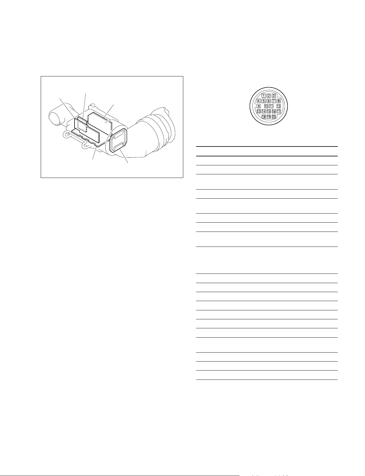
1-1. Location of Printed Circuit Boards 1-2. Connector Input/Output Signals
VF (20P MALE)
VR-266
VDA-41
VF-70
DF-58
LP-105
(EXTERNAL VIEW)
Pin No. Signal I/O Specifications
1 S-DATA IN/OUT TTL level
2NC
3 POWER IN ON : OPEN
OFF CTL OFF : GND
4 SCK IN TTL level
5 COLOR/BW OUT B/W : GND
COLOR : OPEN
6NC
7NC
8 G TALLY IN ON : 5V
OFF : GND
9 PEAKING OUT VF to CAM (Ro = 1 kZ)
CTL 0 V to 5 V
0 V : PEAKING OFF
5 V : PEAKING MAX
10 NC
11 NC
12 Y VIDEO IN 1.0 V p-p (Ro = 75 kZ)
13 VIDEO GND
14 NC
15 NC
16 NC
17 R TALLY IN ON : 5 V
OFF : GND
18 NC
19 UNREG GND
20 UNREG +10.5 V to 17 V
HDVF-20A
1-1 (E)
Page 8
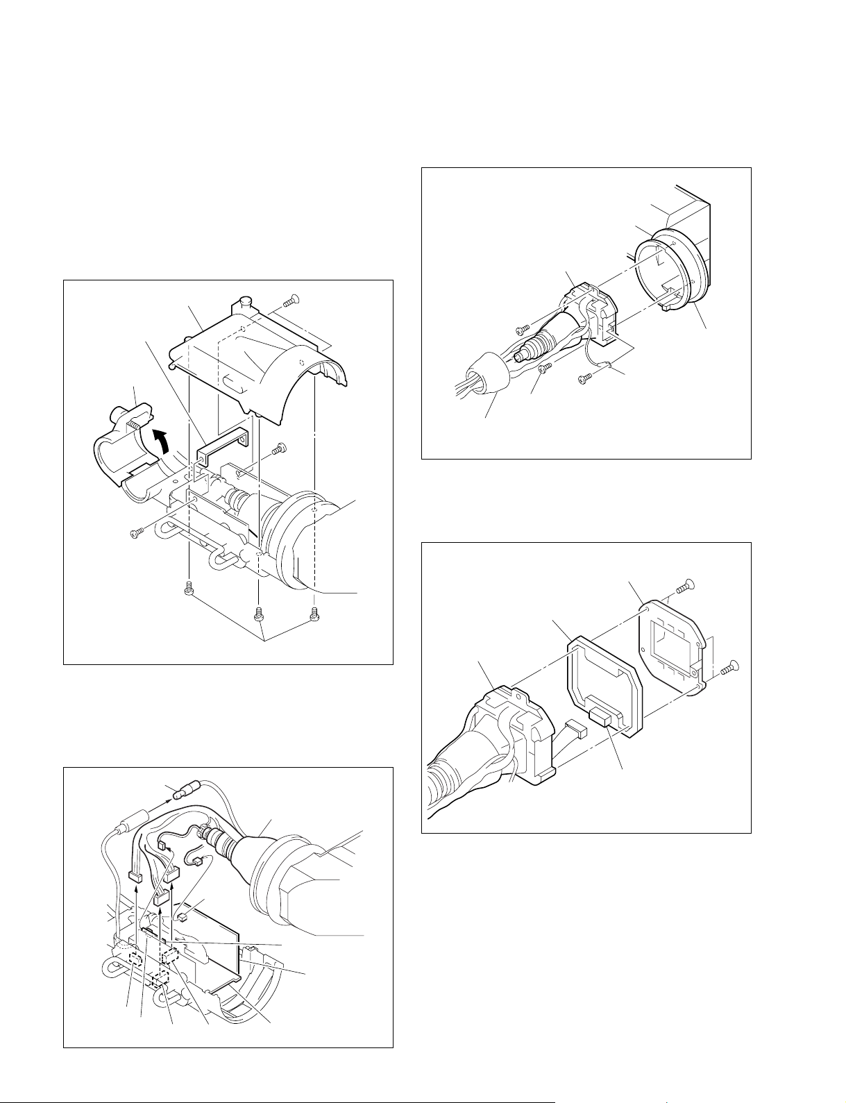
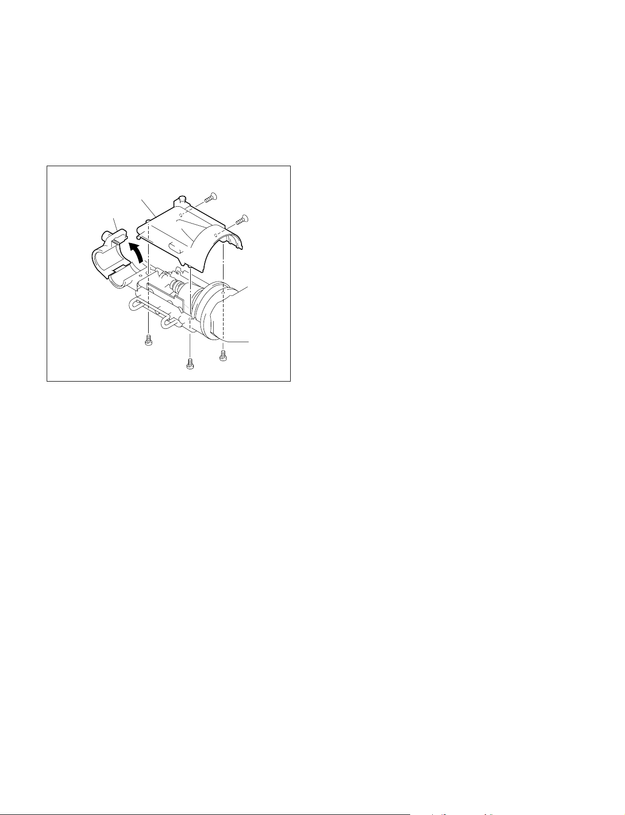
1-3. Replacing CRT
1-3. Replacing CRT
1. Loosen the screw of the MIC clamp and open the MIC
clamp.
2. Remove the two screws (K2.6 x 4).
3. Remove the three hexagonal socket bolts (2.6 x 6) and
remove the upper chassis.
4. Remove the two screws (P2 x 3.5) and the board
bracket.
Upper chassis
Board bracket
MIC clamp
P2 x 3.5
K2.6 x 4
P2 x 3.5
6. Remove the four screws and remove the CRT from the
VF tube assembly.
7. Remove the CRT tube from the CRT.
CRT
PTP2.6 x 8
VF tube
assembly
Lug
PTP2 x 6
PTP2.6 x 8
CRT tube
8. Remove the four screws and remove the microphone
spacer.
9. Disconnect the connector CN21 on the LP-105 board.
Microphone
spacer
K2 x 5
Hexagonal socket bolts 2.6
x 6
5. Disconnect the five connectors CN301, CN501 and
CN502 on the VF-70 board, CN102 on the DF-58
board and CN263 on the VDA-41 board and the anode
cable.
Anode cable
CRT
CN102
VDA-41 board
DF-58 board
CN501
CN263
CN301
CN502
VF-70 board
LP-105 board
CRT
K2 x 5
CN21
10. Install a new CRT in the reverse procedures of
removal.
n
When installing the upper chassis, take care not to
catch the harness between upper and lower chassis.
1-2 (E)
HDVF-20A
Page 9
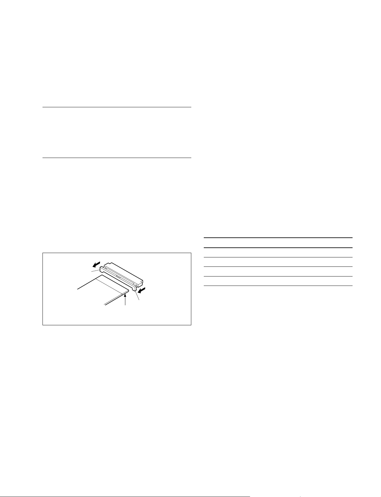
1-4. Disconnecting/Connecting Flexible Card Wire
1-5. Notes on Repair Parts
1-4. Disconnecting/Connecting Flexible
Card Wire
The flexible card wire is used between the VF-70 board
and VR-266 board. Take care not to break this flexible
card wire. This shorten the wire life.
Disconnecting
1. Turn off the power.
2. Slide portions A in the direction of the arrow to unlock
and pull out the flexible card wire.
Connecting
m
. Be careful not to insert the flexible card wire obliquely.
. Check that the conductive surface of the flexible card
wire is not soiled with dust.
1. Slide portions A in the direction of the arrow and
insert the flexible card wire as far as it will go with the
conductive surface down.
2. Slide portions A in the reverse direction to lock.
A
1-5. Notes on Repair Parts
1. Safety Related Components Warning
w
Components marked ! are critical to safe operation.
Therefore, specified parts should be used in the case of
replacement.
2. Standardization of Parts
Some repair parts supplied by Sony differ from those
used for the unit. These are because of parts commonality and improvement.
Parts list has the present standardized repair parts.
3. Stock of Parts
Parts marked with “o” at SP (Supply Code) column of
the spare parts list may not be stocked. Therefore, the
delivery date will be delayed.
4. Units Representation
The following represented units are changed or
omitted in writing.
Units Representation
Capacitance uFuF
Inductance uHuH
Resistance Z Abbreviation
Temperature dC XXX-DEG-C
HDVF-20A
A
Conductive
surface
1-3 (E)
Page 10

1-6. Circuit Description
1-6. Circuit Description
VF-70 board
The VF-70 board consists of a power supply block, H
deflection drive circuit and serial interface circuit for
various controls.
A switching regulator consists of IC401 and Q401 to
Q404, where +9.5 V and about +7.5 V for H driving are
generated from UNREG (10.5 to 17 V) input at pin B10 of
CN001. And H size adjustment is performed by controlling the reference dc voltage for IC401 with RV110 (H
SIZE) on the DF-58 board.
The H deflection circuit IC501 and Q501 are also used to
drive a flyback transformer. The flyback transformer
outputs HV (6 kV), G2 (500 V), 60 V and heater pulse
voltage. The heater pulse voltage is smoothed by C513,
and is adjusted in voltage by RV501 (HEATER). The
resultant is applied to the heater through IC503.
The voltage for feedback circuit is output at pin 1 of the
flyback transformer and is sent to a feedback circuit
consisting of IC501, IC502, Q502 and Q503 to stabilize a
high-voltage portion. When the voltage goes higher than
the reference, the power is turned off as pin 8 of IC502
goes high and a protection circuit operates.
IC301 and IC302 are serial interface ICs, which are used to
control indicators and to grab switch data and so on.
IC304 is a timer IC. It is used to set the time period during
which the zebra pattern is displayed in MOMENTARY
mode, and during which the brightness increases momentarily as the internal tally signal is turned on.
VR-266 board
The VR-266 board consists of a video amplifier circuit and
bright control circuit.
The video signal input at pin 3 of CN201 is adjusted in
level with RV201 (CONTRAST), and is sent through the
peaking circuit to the VDA-41 board.
DC voltage is adjusted with RV205 and RV206 (BRIGHT)
and is sent to the VF-70 board as a bright control voltage.
VDA-41 board
The video signal from the VR-266 board is shifted by a
constant voltage at D261 zener diode. And then the video
signal is amplified by Q261 and Q262, and is output to G1
through a drive circuit of Q263 to Q266. Q267 clamps the
blanking portion to stabilize the black level.
DF-58 board
The DF-58 board provides an external sync circuit, V
deflection drive circuit and blanking pulse generation
circuit.
IC104 is a sync separator, which separates sync signals
from the video signal input to the DF-58 board and outputs
the HD signal from pin 7 and VD signal from pin 3. The
HD signal is compared in phase with a flyback pulse at
IC101 and then enters AFC circuit.
The VD signal is input to pin 21 of IC101, and is then sent
to the V deflection drive circuit consisting of Q104 to
Q107 as a trigger pulse.
IC106 generates a video clamp pulse, and IC108 to IC115
generate a beam blanking pulse. These pulses are output to
the VF-70 board.
1-4 (E)
HDVF-20A
Page 11
Section 2
Electrical Alignment
2-1. General Information for Electrical
Adjustment
2-1-1. Notes on Adjustment
w
There is a danger of an electric shock around the CRT due
to its high voltage. Great care should be taken in servicing.
Never touch a live CRT by bare hands.
Before performing adjustment, read throughly the following comments.
. Calibration for all measuring equipment should be
completed.
. Alignment of peripheral equipment such as camera
should be completed.
2-1-2. Equipment/Fixtures Required
Equipment
. HDVS camera system
HDC-950 or HDW-F900
. AC adaptor
AC-550/550CE or equivalent
. Oscilloscope
(Input capacitance of probe : 12 pF or below)
Tektronix 2465B or equivalent
. HDTV waveform monitor
Tektronix 1735HD/1730HD or equivalent
. HDTV B/W monitor
. Digital voltmeter
. Frequency counter
Fixtures
Fixtures Sony P/N
Pattern box PTB-500 J-6029-140-B
Resolution chart (16:9) J-6395-320-A
VF extension harness J-6395-050-A
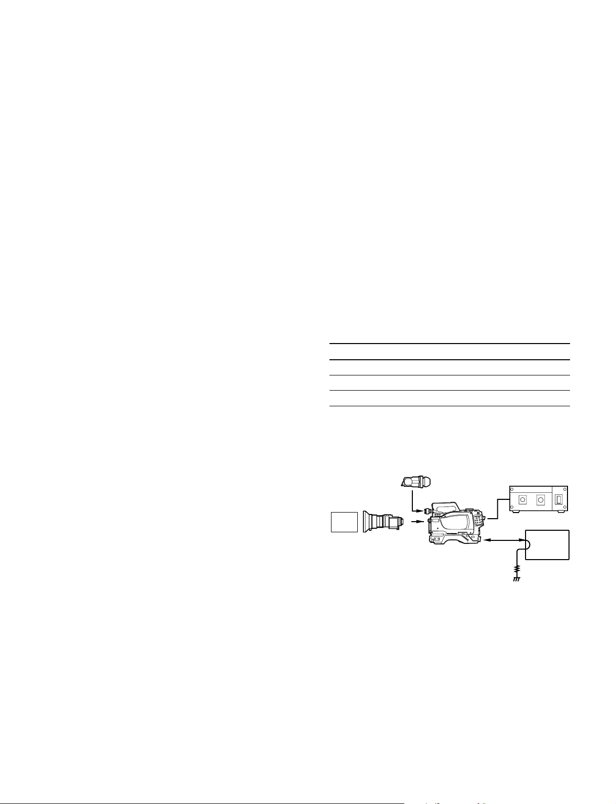
2-1-3. Connection
VIEWFINDER
HDVF-20A
ENG/EFP LENS
PATTERN
BOX
COLOR VIDEO
CAMERA
HDC-950
or HDW-F900
(Figure : HDC-950)
TEST
OUT
75 Z
AC ADAPTOR
AC-550
A-ch
WAVEFORM
MONITOR
HDVF-20A
2-1 (E)
Page 12
2-1-4. Extending Viewfinder
2-1-5. Setting of the VF SCAN Mode
2-1-6. Setting of the Format
2-1-4. Extending Viewfinder
1. Turn off the power before performing adjustment.
2. Remove the viewfinder from the camera.
3. Open the MIC clamp and remove the upper chassis.
(Refer to Section 1-3 “Replacing CRT” for details.)
Upper chassis
MIC clamp
2-1-5. Setting of the VF SCAN Mode
1. Before adjustment, set the VF SCAN mode to 16:9
following to the camera’s setup menu. (Refer to HDC950 or HDW-F900 Operation Manual for details.)
MENU : Operation
PAGE : VF Setup
ITEM : VF Scan → 16:9
2. Whenever you press DISPLAY/SCAN switch on the
viewfinder to SCAN, the picture frame mode toggles
between 16:9 and 4:3. Perform the adjustment in 16:9
mode unless otherwise specified.
2-1-6. Setting of the Format
There are some items which need adjusting by switching
among the each formats of 60i, 50i and 48i.
As for the switching method of the format, refer to the
HDC-950 or HDW-F900 Operation manual. Adjust in the
60i mode unless any specification exists.
4. Connect the viewfinder to the camera via the VF
extension harness.
5. Turn on the power.
2-2 (E)
HDVF-20A
Page 13
DF-58 - component side -
RV120
RV119
RV107
RV106
RV112
RV108
RV101
RV121
RV114
RV113
RV123
CN101
CN102
RV102
RV111
RV116
RV122
RV110
RV109
RV105
RV118
RV117
RV104
RV103
RV115
2-2. Power Supply Voltage Adjustment
2-3. Vertical Hold Adjustment
2-4. Holizontal Hold Adjustment
2-2. Power Supply Voltage Adjustment
Equipment : Digital voltmeter
Adjustment Procedure
Test point : CN101-1pin/DF-58
Adjustment point : 1RV401/VF-70
Specification : 9.50 ±0.05 V dc
2-3. Vertical Hold Adjustment
Equipment : Frequency counter
Adjustment Procedure
Switch the format to 60i, 50i and 48i by the camera and
adjust the following RVs corresponding to each format.
Test point : CN102-1pin/DF-58
GND : Shielding case of FBT501/VF-70
Adjustment point : 1RV105/DF-58 (60i)
1RV117/DF-58 (50i)
1RV118/DF-58 (48i)
Specification : 55.0 ±0.5 Hz
2-4. Horizontal Hold Adjustment
Equipment : Frequency counter
Adjustment Procedure
Switch the format to 60i, 50i and 48i by the camera and
adjust the following RVs corresponding to each format.
Test point : CN101-7pin/DF-58
GND : Shielding case of FBT501/VF-70
Adjustment point : 1RV103/DF-58 (60i)
1RV115/DF-58 (50i)
1RV116/DF-58 (48i)
Specification : 33.75 ±0.25 kHz
HDVF-20A
IC501
RV401
RV501
*Soldering side
FBT501
*TP22
VF-70 - component side -
*TP23
2-3 (E)
Page 14
2-5. Horizontal Duty Adjustment
2-6. Heater Voltage Adjustment
2-5. Horizontal Duty Adjustment
Equipment : Oscilloscope
Preparations
. Iris of the lens : CLOSE
. BRIGHT control : Fully counterclockwise 3
. CONTRAST control : Fully counterclockwise 3
. PEAKING control : Fully counterclockwise 3
Adjustment Procedure
Test point : IC501-7pin/VF-70
GND : Shielding case of FBT501/VF-70
Adjustment point : 1RV104/DF-58
Specification : T = 2.9 ±0.1 us
Turn 1RV104 fully counterclockwise, and slowly turn it
clockwise until the specification
is satisfied.
T
2-6. Heater Voltage Adjustment
Equipment : Digital voltmeter
Note
During adjustment, do not set heater voltage to 700 mV or
over.
Preparations
. BRIGHT control : Mechanical center
. CONTRAST control : Mechanical center
. PEAKING control : Mechanical center
Adjustment Procedure
Test point : TP22/VF-70
GND : TP23/VF-70
Adjustment point : 1RV501/VF-70
Specification : 650 ±30 mV dc
Turn 1RV501 fully clockwise, and
slowly turn it counterclockwise
until the specification is satisfied.
(Do not set heater voltage to
700 mV or over.)
n
If T is set to 2.5 us or below, high-voltage protection
circuit may become activated. In this case, power off once
and turn 1RV104/DF-58 fully counterclockwise. After
that power on again to perform the adjustment.
IC501
RV401
RV501
*Soldering side
FBT501
*TP22
VF-70 - component side -
*TP23
2-4 (E)
HDVF-20A
Page 15
DF-58 - component side -
RV120
RV119
RV107
RV106
RV112
RV108
RV101
RV121
RV114
RV113
RV123
CN101
CN102
RV102
RV111
RV116
RV122
RV110
RV109
RV105
RV118
RV117
RV104
RV103
RV115
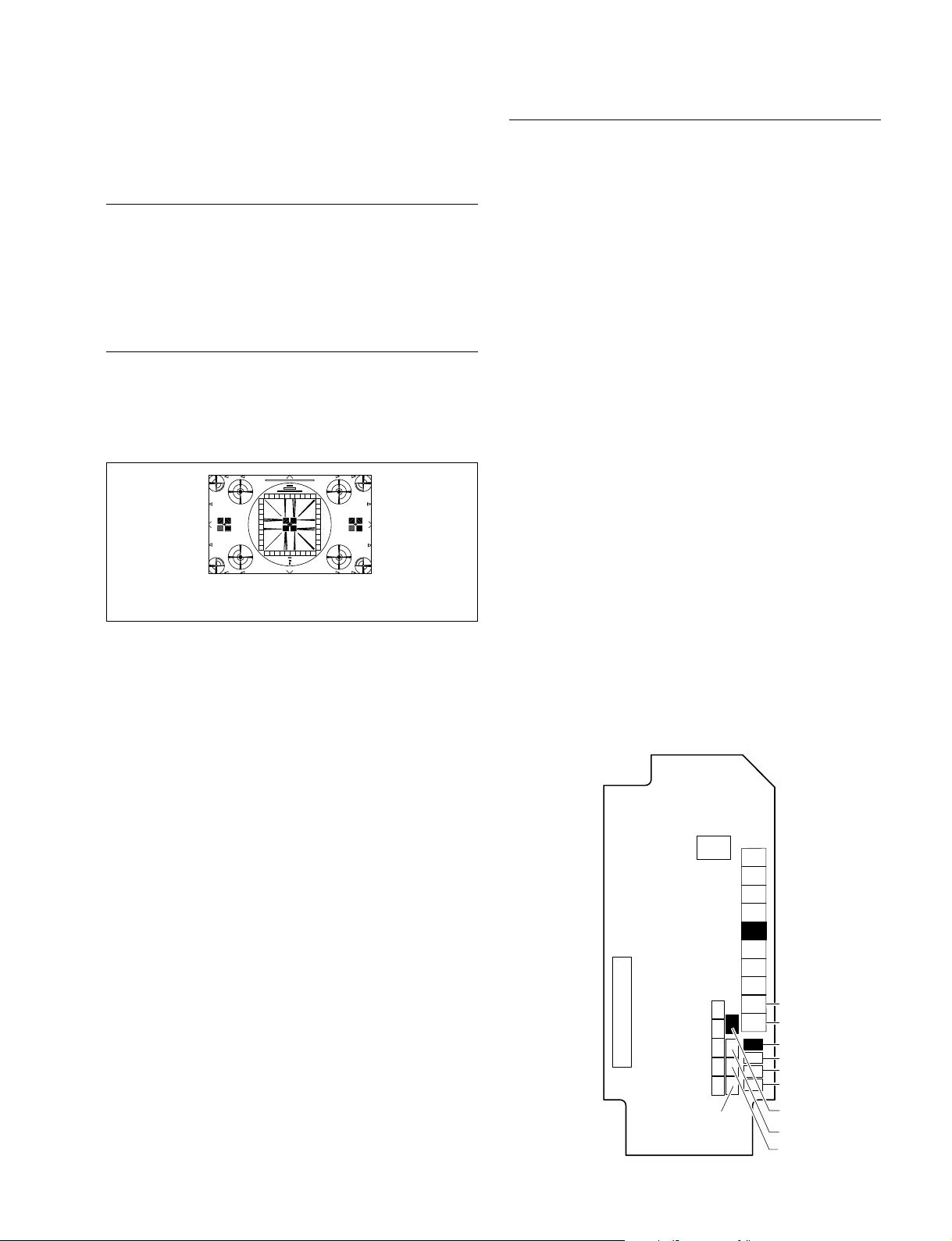
2-7. Focus Adjustment
2-7. Focus Adjustment
Subject : Resolution chart
Note
This focus adjustment, “2-8. Picture Frame Adjustment”
and “2-9. Bright Extent Adjustment” affect each other.
Therefore, repeat these adjustments until all specifications
are satisfied.
Preparations
. Shoot the resolution chart so that the chart frame is
aligned with the underscanned monitor frame with the
zoom control.
Adjustment Procedures
1. Adjustment point : 1RV109/DF-58
Specification : Turn1RV109 fully counter-
clockwise, and slowly turn it
clockwise until the optimum focus
is achieved.
2. After the adjustment, confirm that the focus can be
achieved at all settings of BRIGHT, CONTRAST and
PEAKING controls.
m
. If the picture frame adjustment is out of specifications,
especially in horizontal size, the focus may not be achieved.
In this case, turn 1RV112/DF-58 clockwise a little
(referring to Section 2-8), and perform the focus adjustment.
. The application of too-high voltage may make the high-
voltage protection circuit activated. In this case, power
off once and turn 1RV109/DF-58 fully counterclockwise.
After that power on again to perform the adjustment.
. Adjust the iris of the lens so that the output level (Y
level) at TEST OUT connector on the camera is 500 ±50
mV.
. BRIGHT control : Mechanical center
. CONTRAST control : Mechanical center
. PEAKING control : Fully counterclockwise 3
HDVF-20A
(Viewfinder screen)
2-5 (E)
Page 16

2-8. Picture Frame Adjustment
2-8. Picture Frame Adjustment
Subject : Resolution chart
Note
This picture frame adjustment, “2-7. Focus Adjustment”
and “2-9. Bright Extent Adjustment” affect each other.
Therefore, repeat these adjustments until all specifications
are satisfied.
Preparations
. Shoot the resolution chart so that the chart frame is
aligned with the underscanned monitor frame with the
zoom control.
2. Adjustment points : 1RV112/DF-58
1RV106/DF-58
1Centering magnet
Specification : Adjust 1RV112 and 1RV106
so that the chart frame position
within the CRT frame is as shown
below.Turn the centering magnet
only when centering the chart
About 3 mm
About 1 mm
CRT frame
Chart frame
*1
: Measure on the CRT surface
.
*1
*1
(Viewfinder screen)
.
Adjust the iris of the lens so that the output level (Y level)
at TEST OUT connector on the camera is 500 ±50 mV.
. BRIGHT control : Mechanical center
. CONTRAST control :Mechanical center
. PEAKING control : Fully counterclockwise 3
Adjustment Procedures
1. Vertical Linearity Adjustment
Adjustment point : 1RV108/DF-58
Specification :
Minimize the distortion of the four
circles at the corners of the
resolution chart.
3. Press the portion A to the lower chassis as shown
below to recreate the same situation as when the upper
chassis is installed to the viewfinder, and confirm that
the picture is positioned in the center of the viewfinder.
Centerring magnet
A
2-6 (E)
HDVF-20A
Page 17

DF-58 - component side -
RV120
RV119
RV107
RV106
RV112
RV108
RV101
RV121
RV114
RV113
RV123
CN101
CN102
RV102
RV111
RV116
RV122
RV110
RV109
RV105
RV118
RV117
RV104
RV103
RV115
2-9. Bright Extent Adjustment
Subject : Resolution chart
Note
This bright extent adjustment, “2-7. Focus Adjustment”
and “2-8. Picture Frame Adjustment” affect each other.
Therefore, repeat these adjustments until all specifications
are satisfied.
Preparations
. Shoot the resolution chart so that the chart frame is
aligned with the underscanned monitor frame with the
zoom control.
2-9. Bright Extent Adjustment
.
Adjust the iris of the lens so that the output level (Y level)
at TEST OUT connector on the camera is 500 ±50 mV.
. BRIGHT control : Fully counterclockwise 3
. CONTRAST control : Fully counterclockwise 3
. PEAKING control : Fully counterclockwise 3
Adjustment Procedure
Switch the format to 60i, 50i and 48i by the camera and
adjust the following RVs corresponding to each format.
Adjustment point : 1RV205/VR-266 (60i)
Specification : The central circle of the resolution
HDVF-20A
(Viewfinder screen)
1RV207/VR-266 (50i)
1RV208/VR-266 (48i)
chart shall be barely discriminated.
RV-204
RV-201
RV-206
RV-203
RV-202
RV-207
RV-205
RV-208
VR-266 - component side -
2-7 (E)
Page 18

DF-58 - component side -
RV120
RV119
RV107
RV106
RV112
RV108
RV101
RV121
RV114
RV113
RV123
CN101
CN102
RV102
RV111
RV116
RV122
RV110
RV109
RV105
RV118
RV117
RV104
RV103
RV115
2-10. Horizontal Picture Positioning Adjustment
2-10. Horizontal Picture Positioning
Adjustment
Subject : Resolution chart
Preparations
. Shoot the resolution chart so that the chart frame is
aligned with the underscanned monitor frame with the
zoom control.
(Viewfinder screen)
.
Adjust the iris of the lens so that the output level (Y level)
at TEST OUT connector on the camera is 500 ±50 mV.
. BRIGHT control : Fully clockwise 2
. CONTRAST control :Fully counterclockwise 3
. PEAKING control : Fully counterclockwise 3
Adjustment Procedure
Switch the format to 60i, 50i and 48i by the camera and
adjust the following RVs corresponding to each format.
Adjustment point : 1RV101/DF-58 (60i)
Specification : Adjust the position of the resolu-
A B
2-8 (E)
1RV121/DF-58 (50i)
1RV122/DF-58 (48i)
tion chart for A = B
Underscanned monitor frame (raster)
Chart frame
RV-204
RV-201
RV-206
RV-203
RV-202
RV-207
RV-205
RV-208
VR-266 - component side -
HDVF-20A
Page 19

2-11. Peaking Level Adjustment
2-12. Clamping Level Adjustment
2-11. Peaking Level Adjustment
Equipment : Oscilloscope
Subject : Resolution chart
Preparations
. Shoot the resolution chart so that the chart frame is
aligned with the underscanned monitor frame with the
zoom control.
(Viewfinder screen)
.
Adjust the iris of the lens so that the output level (Y level)
at TEST OUT connector on the camera is 500 ±50 mV.
. BRIGHT control : Mechanical center
. CONTRAST control : Mechanical center
. PEAKING control : Fully counterclockwise 3
2-12. Clamping Level Adjustment
Equipment : Oscilloscope (DC mode)
(Input capacitance of probe : 12 pF or below)
Subject : Resolution chart
Preparations
. Shoot the resolution chart so that the chart frame is
aligned with the underscanned monitor frame with the
zoom control.
(Viewfinder screen)
.
Adjust the iris of the lens so that the output level (Y level)
at TEST OUT connector on the camera is 500 ±50 mV.
. BRIGHT control : Mechanical center
. CONTRAST control :Mechanical center
. PEAKING contro : Fully counterclockwise 3
Adjustment Procedure
Test point : TP261/VDA-41
GND : Viewfinder cabinet
Adjustment point : 1RV203/VR-266
Specification : The waveform level A shall not
change at all settings of PEAKING control.
A
Adjustment Procedure
Test point : TP261/VDA-41
GND : Grounding plate/VR-266
Adjustment point : 1RV202/VR-266
Specifications : Adjust the overshoot A for 9 ±1 V.
Check to see that blanking B is
from 5 V to 20 V.
A
Pedestal Level
B
TP261
HDVF-20A
VDA-41 - soldering side -
2-9 (E)
Page 20

DF-58 - component side -
RV120
RV119
RV107
RV106
RV112
RV108
RV101
RV121
RV114
RV113
RV123
CN101
CN102
RV102
RV111
RV116
RV122
RV110
RV109
RV105
RV118
RV117
RV104
RV103
RV115
2-13. 4:3 Picture Frame Adjustment
2-13. 4:3 Picture Frame Adjustment
Subject : Full white pattern
Preparations
. Shoot the fully occupied white area in the underscanned
monitor frame with the zoom control.
.
Adjust the iris of the lens so that the output level (Y level)
at TEST OUT connector on the camera is 350 ±35 mV.
. BRIGHT control : Fully clockwise 2
. CONTRAST control :Mechanical center
. PEAKING control : Mechanical center
. Press the DISPLAY/ASPECT switch to ASPECT to
enter the 4:3 mode.
Adjustment Procedure
Adjustment points : 1RV102 (4:3 PHASE)/DF-58
1RV111 (4:3 SIZE)/DF-58
Specifications : Adjust the 4:3 picture frame for
A = 2 ±1 mm with 1RV102 and
1 RV111. (Adjust the gray area)
Setting after Adjustment
Press the DISPLAY/ASPECT switch to ASPECT to return
the 16:9 mode.
2-10 (E)
A AGray area
*1 Measure on the CRT surface
*1
HDVF-20A
Page 21

3-1. Exploded Views
Section 3
Spare Parts
13
19
30
17
21
26
6
20
10
B2 x 4
27
29
Precision
18
P2 x 3.5
1
B2 x 4
11
K2.6 x 5
24
24
16
4
BOLT, HEXAGON
SOCKET 2.6 x 6
8
9
Precision
2 12
P2 x 3.5
7
5
25
Precision
P2 x 3.5
14
3
15
BOLT, HEXAGON
23
BOLT, HEXAGON
SOCKET 2.6 x 6
No. Part No. SP Description
1 1-761-333-11 o MOUNTED CIRCUIT BOARD, VF-70
2 1-761-334-11 o MOUNTED CIRCUIT BOARD, DF-58
3 1-761-335-11 o MOUNTED CIRCUIT BOARD, VR-266
4 X-3678-575-3 o CHASSIS B ASSY,BOTTOM(LOWER)
5 1-761-339-11 o MOUNTED CIRCUIT BOARD, VDA-41
6 1-777-131-22 s CORD, CONNECTION (VF)
7 9-885-005-93 o CABLE, FLAT (12 CORE)
8 2-277-457-01 s KNOB, STOPPER
9 2-277-466-01 s SPRING, COMPRESSION
10 3-165-904-01 s WASHER, SCREW STOPPER
11 3-609-582-01 o PLATE, BOARD FIX
12 3-609-583-01 o SHEET, INSULATING
SOCKET 2.6 x 6
28
Precision
P2 x 3.5
No. Part No. SP Description
18 3-692-132-03 o COVER,TALLY
19 3-692-134-01 o MIC CLAMP
20 3-692-138-01 s MIC CUSHION,RUBBER
21 X-3604-579-1 s VOLUME KNOB ASSY
23 3-609-735-01 o BAR, GUARD
24 3-697-152-01 o SPRING,LEAF(2)
25 3-697-153-01 o PLATE,GROUND(2)
26 A-8277-112-A o CASE ASSY, TOP
27 3-697-156-01 o CUSHION,DRROP PROTECCTION(2)
28 3-697-161-01 o LID,COVER
29 3-710-008-02 s HOUSING, STOPPER
30 3-697-160-01 o LABEL, VF (C)
13 3-657-657-02 s SCREW (M5)
14 3-679-693-01 o BASE,SLIDE
15 3-679-694-01 o COVER,SLIDE
7-621-772-18 s SCREW, +B 2X4
7-627-454-38 s SCREW, PRECISION +K 2.6X5
7-627-554-18 s SCREW,PRECISION +P 2X3.5 TYPE1
16 3-679-695-01 o COVER,TALLY
7-683-412-05 s BOLT,HEXAGON SOCKET 2.6X6
17 3-693-327-01 s NUT (M6), CONTROL
HDVF-20A
3-1
Page 22

120
PTP2.6 x 8
P2 x 6
128
102
PTP2.6 x 8
110
101
108
113
118
110
103
K2 x 5
122
107
P2 x 6
111
K2 x 5
125
116
115
112
105
114
Ball 2.5 dia
106
115
105
121
124
109
106
104
Ball
2.5 dia
Precision
P2 x 10
123
117
127
119
104
Precision
P2 x 10
122126
No. Part No. SP Description
101 A-7612-389-B s TUBE SUB ASSY, VF
102 ! 1-251-636-11 s CRT ASSY, 2" HD
103 A-8315-579-A o MOUNTED CIRCUIT BOARD, LP-105
104 3-176-414-01 o RETAINER, RING
105 3-335-207-01 s SHAFT, MOTOR
106 3-573-150-00 o SPRING, COMPRESSION
107 3-603-499-02 s SPACER, MASK
108 3-608-806-01 o MIRROR(3)
109 3-692-136-03 o FIXED RING
110 3-692-144-01 o SPACER, LP
111 3-697-159-02 o PLATE A,DISPLAY
No. Part No. SP Description
118 3-723-073-01 o CUSHION, MIRROR
119 A-8319-943-A s EYE CUP (RP)
120 3-725-220-02 o TUBE (A), CRT
121 3-726-904-01 o RING (MT), O
122 3-742-038-01 o NUT (2), PLATE
123 3-742-052-03 o HOLDER, EYECUP
124 3-742-053-02 o RING
125 3-742-054-01 o TUBE
126 3-742-060-01 o HOLDER, RING
127 3-623-709-01 o MC HOLDER
128 9-885-005-86 o SOKET, CRT
112 3-697-151-01 o RING,VF
113 3-697-154-01 o HOLDER,MIRROR(3)
114 3-697-167-03 o VF TUBE(4)
115 3-722-485-01 o ROLLER, SLIDE
7-627-452-38 s SCREW,PRECISION +K 2X5
7-627-553-78 s SCREW,PRECISION +P 2X10
7-671-158-01 s BALL, STAINLESS (2.5 DIA)
7-685-104-19 s SCREW +P 2X6 TYPE2 NON-SLIT
116 3-722-492-01 o HOLDER (B), LENS
7-685-134-19 s SCREW +PTP 2.6X8 TYPE2 NON-SLIT
117 3-623-710-01 o MC, GLASS
7-685-104-14 s SCREW +P 2X6 TYPE2 NON-SLIT
3-2
HDVF-20A
Page 23

3-2. Electrical Parts List
----------DF-58 Board
---------- Ref. No.
or Q'ty Part No. SP Description
(DF-58 Board)
Ref. No.
or Q'ty Part No. SP Description
1pc 1-761-334-11 o MOUNTED CIRCUIT BOARD, DF-58
D101 8-719-951-22 s DIODE IMN10
D103 8-719-941-23 s DIODE DA204U
C101 1-115-581-11 s TANTALUM,CHIP 100uF 20% 16
D104 8-719-056-22 s DIODE MA2S728-(K8).SO
C102 1-104-913-11 s TANTALUM, CHIP 10uF 20% 16V
C103 1-115-581-11 s TANTALUM,CHIP 100uF 20% 16
C104 1-163-251-11 s CERAMIC, CHIP 100PF 5% 50V
C105 1-164-691-11 s CERAMIC 0.0024uF 5% 50V
IC101 ! 8-759-394-25 s IC LA7858
IC102 8-759-075-70 s IC TA75S393F
IC103 8-759-234-08 s IC TA78L05F
IC104 8-759-394-30 s IC GS4981IKA
C106 1-163-135-00 s CERAMIC 560PF 5% 50V
IC105 8-759-242-78 s IC TC7W02F
C107 1-164-182-11 s CERAMIC 0.0033uF 10% 50V
C108 1-135-091-00 s TANTALUM, CHIP 1uF 20% 16V
C109 1-135-091-00 s TANTALUM, CHIP 1uF 20% 16V
C110 1-104-551-11 s FILM 0.01uF 5% 16V
IC106 8-759-180-08 s IC TC74HC4538AFS
IC107 8-759-058-62 s IC TC7S08FU(TE85R)
IC108 8-759-082-61 s IC TC4W53FU
IC109 8-759-180-08 s IC TC74HC4538AFS
C111 1-104-542-11 s CHIP FILM 0.0018uF 5% 50V
IC110 8-759-394-32 s IC TC4427EOA
C112 1-163-145-00 s CERAMIC 0.0015uF 10% 50V
C113 1-164-004-11 s CERAMIC, CHIP 0.1uF 10% 25V
C114 1-104-913-11 s TANTALUM, CHIP 10uF 20% 16V
C115 1-115-581-11 s TANTALUM,CHIP 100uF 20% 16
IC111 8-759-082-59 s IC TC7W32FU
IC112 8-759-180-08 s IC TC74HC4538AFS
IC113 8-759-058-64 s IC TC7S32FU(TE85R)
IC114 8-759-082-55 s IC TC7W00FU
C116 1-135-070-00 s TANTALUM, CHIP 0.1uF 10% 35V
IC115 8-759-180-08 s IC TC74HC4538AFS
C117 1-135-179-21 s TANTAL 2.2uF 10% 16V
C118 1-135-145-11 s TANTALUM, CHIP 0.47uF 10% 35V
IC116 8-759-180-08 s IC TC74HC4538AFS
C119 1-164-004-11 s CERAMIC, CHIP 0.1uF 10% 25V
C120 1-163-251-11 s CERAMIC, CHIP 100PF 5% 50V
Q101 8-729-802-80 s TRANSISTOR 2SC3661
Q102 8-729-042-52 s TRANSISTOR IMT1AT108
C121 1-115-581-11 s TANTALUM,CHIP 100uF 20% 16
C122 1-104-913-11 s TANTALUM, CHIP 10uF 20% 16V
C123 1-163-018-00 s CERAMIC, CHIP 0.0056uF 5% 50V
Q103 8-729-042-52 s TRANSISTOR IMT1AT108
Q104 8-729-905-36 s TRANSISTOR 2SC4081-S
Q105 8-729-402-84 s TRANSISTOR XN4601
C124 9-885-005-12 s ELECT, CHIP 470uF 16V
C125 1-163-021-91 s CERAMIC 0.01uF 10% 50V
Q106 8-729-905-36 s TRANSISTOR 2SC4081-S
Q107 8-729-905-36 s TRANSISTOR 2SC4081-S
C126 1-115-185-11 s CERAMIC 0.033uF 10% 25V
C127 1-163-275-11 s CERAMIC, CHIP 1000PF 5% 50V
C128 1-163-275-11 s CERAMIC, CHIP 1000PF 5% 50V
Q108 8-729-905-36 s TRANSISTOR 2SC4081-S
Q109 8-729-036-19 s TRANSISTOR IMB2A
Q110 8-729-425-41 s TRANSISTOR 2SK1374
C129 1-164-004-11 s CERAMIC, CHIP 0.1uF 10% 25V
C130 1-164-004-11 s CERAMIC, CHIP 0.1uF 10% 25V
Q111 8-729-425-41 s TRANSISTOR 2SK1374
Q112 8-729-026-53 s TRANSISTOR 2SA1576A-T106-QR
C131 1-164-004-11 s CERAMIC, CHIP 0.1uF 10% 25V
C151 1-104-913-11 s TANTALUM, CHIP 10uF 20% 16V
C152 1-107-686-11 s CHIP, TANTALUM 4.7uF 20% 16V
Q113 8-729-042-52 s TRANSISTOR IMT1AT108
Q114 8-729-028-91 s TRANSISTOR DTA144EUA-T106
Q115 8-729-036-19 s TRANSISTOR IMB2A
C153 1-163-235-11 s CERAMIC, CHIP 22PF 5% 50V
C154 1-107-686-11 s CHIP, TANTALUM 4.7uF 20% 16V
R101 1-216-833-11 s METAL, CHIP 10K 5% 1/16W
R102 1-216-825-11 s METAL, CHIP 2.2K 5% 1/16W
C155 1-164-004-11 s CERAMIC, CHIP 0.1uF 10% 25V
C156 1-164-004-11 s CERAMIC, CHIP 0.1uF 10% 25V
C157 1-163-235-11 s CERAMIC, CHIP 22PF 5% 50V
R103 1-216-837-11 s METAL, CHIP 22K 5% 1/16W
R104 1-216-834-11 s METAL, CHIP 12K 5% 1/16W
R105 1-216-832-11 s METAL, CHIP 8.2K 5% 1/16W
C158 1-163-251-11 s CERAMIC, CHIP 100PF 5% 50V
C159 1-164-004-11 s CERAMIC, CHIP 0.1uF 10% 25V
R106 1-216-845-11 s METAL, CHIP 100K 5% 1/16W
R107 1-216-832-11 s METAL, CHIP 8.2K 5% 1/16W
C160 1-163-251-11 s CERAMIC, CHIP 100PF 5% 50V
C161 9-885-005-13 s CAPACITOR, PP 0.0015uF 100V
C162 9-885-005-13 s CAPACITOR, PP 0.0015uF 100V
R108 1-216-839-11 s METAL, CHIP 33K 5% 1/16W
R109 1-218-345-11 s METAL, CHIP 9.1K 5% 1/16W
R110 1-216-821-11 s METAL, CHIP 1K 5% 1/16W
C163 1-163-235-11 s CERAMIC, CHIP 22PF 5% 50V
C164 1-164-004-11 s CERAMIC, CHIP 0.1uF 10% 25V
R111 1-218-294-11 s METAL, CHIP 30K 5% 1/16W
R112 1-216-836-11 s METAL, CHIP 18K 5% 1/16W
C171 1-115-419-11 s CERAMIC 0.0033uF 10% 25V
C172 1-164-004-11 s CERAMIC, CHIP 0.1uF 10% 25V
C175 1-163-235-11 s CERAMIC, CHIP 22PF 5% 50V
R114 1-218-830-11 s METAL, CHIP 5.6K 5% 1/16W
R115 1-216-798-11 s METAL, CHIP 12 5% 1/16W
R116 1-216-848-11 s METAL, CHIP 180K 5% 1/16W
C176 1-164-004-11 s CERAMIC, CHIP 0.1uF 10% 25V
C182 1-163-135-00 s CERAMIC 560PF 5% 50V
R117 1-216-846-11 s METAL, CHIP 120K 5% 1/16W
R118 1-216-822-11 s METAL, CHIP 1.2K 5% 1/16W
C183 1-163-251-11 s CERAMIC, CHIP 100PF 5% 50V
C184 1-163-275-11 s CERAMIC, CHIP 1000PF 5% 50V
C185 1-164-004-11 s CERAMIC, CHIP 0.1uF 10% 25V
R119 1-216-845-11 s METAL, CHIP 100K 5% 1/16W
R120 1-218-272-11 s METAL, CHIP 5.1K 5% 1/16W
R121 1-218-272-11 s METAL, CHIP 5.1K 5% 1/16W
C186 1-163-235-11 s CERAMIC, CHIP 22PF 5% 50V
C187 1-163-275-11 s CERAMIC, CHIP 1000PF 5% 50V
R122 1-216-813-11 s METAL, CHIP 220 5% 1/16W
R123 1-216-308-00 s METAL, CHIP 4.7 5% 1/10W
CN102 1-564-704-11 s CONNECOR, 2P, MALE
R124 1-216-829-11 s METAL, CHIP 4.7K 5% 1/16W
HDVF-20A
3-3
Page 24

(DF-58 Board)
(DF-58 Board)
Ref. No.
or Q'ty Part No. SP Description
R125 1-216-827-11 s METAL, CHIP 3.3K 5% 1/16W
R126 1-216-308-00 s METAL, CHIP 4.7 5% 1/10W
R127 1-216-308-00 s METAL, CHIP 4.7 5% 1/10W
R128 1-216-037-00 s METAL, CHIP 330 5% 1/10W
R129 1-216-801-11 s METAL, CHIP 22 5% 1/16W
Ref. No.
or Q'ty Part No. SP Description
R186 1-216-841-11 s METAL, CHIP 47K 5% 1/16W
R187 1-216-821-11 s METAL, CHIP 1K 5% 1/16W
R188 1-216-821-11 s METAL, CHIP 1K 5% 1/16W
R189 1-216-821-11 s METAL, CHIP 1K 5% 1/16W
R190 1-216-850-11 s METAL, CHIP 270K 5% 1/16W
1-216-849-11 s METAL, CHIP 220K 5% 1/16W
R130 1-216-308-00 s METAL, CHIP 4.7 5% 1/10W
R131 1-216-821-11 s METAL, CHIP 1K 5% 1/16W
R132 1-216-816-11 s METAL, CHIP 330 5% 1/16W
R191 1-216-850-11 s METAL, CHIP 270K 5% 1/16W
1-216-849-11 s METAL, CHIP 220K 5% 1/16W
R133 1-216-818-11 s METAL, CHIP 560 5% 1/16W
R134 1-218-272-11 s METAL, CHIP 5.1K 5% 1/16W
RV101 9-885-005-14 s RES, ADJ METAL 5K
RV102 9-885-005-09 s RES, ADJ METAL 4.7K
R135 1-216-836-11 s METAL, CHIP 18K 5% 1/16W
R136 1-216-829-11 s METAL, CHIP 4.7K 5% 1/16W
R137 1-216-832-11 s METAL, CHIP 8.2K 5% 1/16W
RV103 9-885-005-09 s RES, ADJ METAL 4.7K
RV104 9-885-005-09 s RES, ADJ METAL 4.7K
RV105 9-885-005-15 s RES, ADJ METAL 220K
R138 1-216-825-11 s METAL, CHIP 2.2K 5% 1/16W
R139 1-218-331-11 s METAL, CHIP 51K 50% 1/16W
RV106 9-885-005-16 s RES, ADJ METAL 200
RV107 9-885-005-14 s RES, ADJ METAL 5K
R140 1-216-835-11 s METAL, CHIP 15K 5% 1/16W
R141 1-216-833-11 s METAL, CHIP 10K 5% 1/16W
R142 1-216-836-11 s METAL, CHIP 18K 5% 1/16W
RV108 9-885-005-14 s RES, ADJ METAL 5K
RV109 9-885-005-09 s RES, ADJ METAL 4.7K
RV110 9-885-005-14 s RES, ADJ METAL 5K
R143 1-218-272-11 s METAL, CHIP 5.1K 5% 1/16W
R144 1-216-816-11 s METAL, CHIP 330 5% 1/16W
RV111 9-885-005-09 s RES, ADJ METAL 4.7K
RV112 9-885-005-17 s RES, ADJ METAL 50K
R145 1-216-816-11 s METAL, CHIP 330 5% 1/16W
R146 1-216-816-11 s METAL, CHIP 330 5% 1/16W
R147 1-216-816-11 s METAL, CHIP 330 5% 1/16W
RV113 9-885-005-09 s RES, ADJ METAL 4.7K
RV114 9-885-005-10 s RES, ADJ METAL 47K
RV115 9-885-005-18 s RES, ADJ METAL 470
R148 1-216-841-11 s METAL, CHIP 47K 5% 1/16W
R149 1-216-841-11 s METAL, CHIP 47K 5% 1/16W
RV116 9-885-005-19 s RES, ADJ METAL 1K
RV117 9-885-005-19 s RES, ADJ METAL 1K
R151 1-216-841-11 s METAL, CHIP 47K 5% 1/16W
R152 1-216-825-11 s METAL, CHIP 2.2K 5% 1/16W
R153 1-216-825-11 s METAL, CHIP 2.2K 5% 1/16W
RV118 9-885-005-09 s RES, ADJ METAL 4.7K
RV119 9-885-005-20 s RES, ADJ METAL 500
RV120 9-885-005-20 s RES, ADJ METAL 500
R154 1-216-833-11 s METAL, CHIP 10K 5% 1/16W
R155 1-216-851-11 s METAL, CHIP 330K 5% 1/16W
RV121 9-885-005-14 s RES, ADJ METAL 5K
RV122 9-885-005-14 s RES, ADJ METAL 5K
R156 1-216-813-11 s METAL, CHIP 220 5% 1/16W
R157 1-216-833-11 s METAL, CHIP 10K 5% 1/16W
R158 1-216-993-11 s METAL, CHIP 2.4K 5% 1/16W
R159 1-216-827-11 s METAL, CHIP 3.3K 5% 1/16W
R160 1-216-827-11 s METAL, CHIP 3.3K 5% 1/16W
R161 1-216-821-11 s METAL, CHIP 1K 5% 1/16W
R162 1-216-826-11 s METAL, CHIP 2.7K 5% 1/16W
R163 1-216-994-11 s METAL, CHIP 13K 5% 1/16W
R164 1-216-813-11 s METAL, CHIP 220 5% 1/16W
R165 1-216-801-11 s METAL, CHIP 22 5% 1/16W
R166 1-216-816-11 s METAL, CHIP 330 5% 1/16W
R167 1-216-816-11 s METAL, CHIP 330 5% 1/16W
R168 1-216-816-11 s METAL, CHIP 330 5% 1/16W
R169 1-216-816-11 s METAL, CHIP 330 5% 1/16W
R171 1-216-834-11 s METAL, CHIP 12K 5% 1/16W
R172 1-218-292-11 s METAL, CHIP 20K 5% 1/16W
R173 1-216-839-11 s METAL, CHIP 33K 5% 1/16W
R174 1-216-994-11 s METAL, CHIP 13K 5% 1/16W
R175 1-220-372-11 s METAL, CHIP 200K 5% 1/16W
1-216-848-11 s METAL, CHIP 180K 5% 1/16W
1-216-861-11 s METAL, CHIP 220K 5% 1/16W
R176 1-216-827-11 s METAL, CHIP 3.3K 5% 1/16W
R178 1-216-801-11 s METAL, CHIP 22 5% 1/16W
R179 1-216-818-11 s METAL, CHIP 560 5% 1/16W
R180 1-216-801-11 s METAL, CHIP 22 5% 1/16W
R181 1-218-830-11 s METAL, CHIP 5.6K 5% 1/16W
R182 1-218-830-11 s METAL, CHIP 5.6K 5% 1/16W
R183 1-218-271-11 s METAL, CHIP 2K 5% 1/16W
R184 1-216-809-11 s METAL, CHIP 100 5% 1/16W
R185 1-216-809-11 s METAL, CHIP 100 5% 1/16W
3-4
HDVF-20A
Page 25

-----------LP-105 Board
----------- Ref. No.
or Q'ty Part No. SP Description
-----------VDA-41 Board
----------- Ref. No.
or Q'ty Part No. SP Description
1pc A-8315-579-A o MOUNTED CIRCUIT BOARD, LP-105
CN21 1-565-651-11 o PIN, CONNECTOR 8P
1pc 1-761-339-11 o MOUNTED CIRCUIT BOARD, VDA-41
C261 1-110-497-11 s CERAMIC, CHIP 0.1uF 20% 100V
C262 1-163-259-91 s CERAMIC 220PF 5% 50V
D1 8-729-026-39 s TRANSISTOR 2SA933AS-QT
D2 8-719-026-40 s DIODE CL-150UR-CD-T
D3 8-719-987-43 s DIODE CL-150PG-CD
C263 1-164-004-11 s CERAMIC, CHIP 0.1uF 10% 25V
C264 1-110-497-11 s CERAMIC, CHIP 0.1uF 20% 100V
C265 1-164-004-11 s CERAMIC, CHIP 0.1uF 10% 25V
D4 8-719-026-16 s DIODE CL-150D-CD-T
D5 8-719-026-40 s DIODE CL-150UR-CD-T
D261 8-719-984-56 s DIODE HZK2ALL
D262 8-719-052-18 s DIODE RLS245TE-11
D6 8-719-026-16 s DIODE CL-150D-CD-T
Q261 8-729-036-39 s TRANSISTOR 2SC4104
Q262 8-729-036-38 s TRANSISTOR 2SC4080
Q263 8-729-036-39 s TRANSISTOR 2SC4104
Q264 8-729-036-40 s TRANSISTOR 2SA1580
Q265 8-729-036-39 s TRANSISTOR 2SC4104
Q266 8-729-036-40 s TRANSISTOR 2SA1580
Q267 8-729-036-39 s TRANSISTOR 2SC4104
R261 1-218-289-11 s METAL, CHIP 510 5% 1/16W
R262 1-202-923-91 s METAL, CHIP 130 5% 1/16W
R263 9-885-005-00 s METAL, CHIP 3.9K
R264 1-216-809-11 s METAL, CHIP 100 5% 1/16W
R265 1-216-833-11 s METAL, CHIP 10K 5% 1/16W
R266 1-216-809-11 s METAL, CHIP 100 5% 1/16W
R267 1-216-834-11 s METAL, CHIP 12K 5% 1/16W
R268 1-216-809-11 s METAL, CHIP 100 5% 1/16W
R269 1-216-834-11 s METAL, CHIP 12K 5% 1/16W
R270 1-216-809-11 s METAL, CHIP 100 5% 1/16W
R271 1-216-809-11 s METAL, CHIP 100 5% 1/16W
R272 1-216-803-11 s METAL, CHIP 33 5% 1/16W
R273 1-216-803-11 s METAL, CHIP 33 5% 1/16W
R274 1-218-179-11 s RES, CHIP 10M 5% 1/10W
R275 1-218-289-11 s METAL, CHIP 510 5% 1/16W
R276 1-218-273-11 s METAL, CHIP 510K 5% 1/16W
R277 1-216-033-00 s METAL, CHIP 220 5% 1/10W
HDVF-20A
3-5
Page 26

----------VF-70 Board
---------- Ref. No.
or Q'ty Part No. SP Description
(VF-70 Board)
Ref. No.
or Q'ty Part No. SP Description
1pc 1-761-333-11 o MOUNTED CIRCUIT BOARD, VF-70
D306 8-719-056-80 s DIODE UDZ5.1B
D307 8-719-056-80 s DIODE UDZ5.1B
C301 1-164-004-11 s CERAMIC, CHIP 0.1uF 10% 25V
C302 1-164-004-11 s CERAMIC, CHIP 0.1uF 10% 25V
C303 1-164-004-11 s CERAMIC, CHIP 0.1uF 10% 25V
D401 8-719-989-76 s DIODE SC802-04
D402 8-719-989-76 s DIODE SC802-04
D501 8-719-941-23 s DIODE DA204U
C304 1-164-004-11 s CERAMIC, CHIP 0.1uF 10% 25V
C305 1-164-004-11 s CERAMIC, CHIP 0.1uF 10% 25V
D502 8-719-941-23 s DIODE DA204U
D503 8-719-941-23 s DIODE DA204U
C306 1-135-160-21 s CHIP, TANTALUM 15uF 10% 16V
C307 1-107-686-11 s CHIP, TANTALUM 4.7uF 20% 16V
C308 1-164-001-11 s CERAMIC 150PF 5% 50V
D504 8-719-941-86 s DIODE DAN202U
D505 8-719-941-23 s DIODE DA204U
D506 8-719-941-86 s DIODE DAN202U
C309 1-104-913-11 s TANTALUM, CHIP 10uF 20% 16V
C310 1-164-001-11 s CERAMIC 150PF 5% 50V
C311 1-164-004-11 s CERAMIC, CHIP 0.1uF 10% 25V
D507 8-759-394-26 s IC LM4041EIM3-1.2
FBT1 ! 1-453-243-11 s TRANSFORMER, FLYBACK
C312 1-164-004-11 s CERAMIC, CHIP 0.1uF 10% 25V
C401 9-885-005-02 s ELECT 220uF 25V
HLC1 ! 1-416-387-11 s COIL, LINEARITY
C402 1-135-091-00 s TANTALUM, CHIP 1uF 20% 16V
C403 1-164-686-91 s CERAMIC 0.0015 5% 50V
IC301 8-759-990-61 s IC PCF8574T
IC302 8-759-990-61 s IC PCF8574T
C404 1-104-919-11 s TANTALUM, CHIP 10uF 20% 25V
C405 1-163-275-91 s CERAMIC 0.001 5% 50V
C406 1-164-001-11 s CERAMIC 150PF 5% 50V
IC303 8-759-394-34 s IC BR24C02F
IC304 8-759-939-51 s IC BA225F
IC305 8-759-082-59 s IC TC7W32FU
C407 9-885-005-03 s CAPACITOR, OS 150uF 16V
C408 1-104-913-11 s TANTALUM, CHIP 10uF 20% 16V
IC306 8-759-209-57 s IC TC4S69F
IC401 8-759-485-77 s IC BA9743AFV-E2
C409 1-107-686-11 s CHIP, TANTALUM 4.7uF 20% 16V
C410 1-163-251-91 s CERAMIC 0.0001 5% 50V
C411 1-164-686-91 s CERAMIC 0.0015 5% 50V
IC501 8-759-394-31 s IC TC4426EOA
IC502 8-759-060-00 s IC BA10324AF
IC503 8-759-075-66 s IC TA75S01F
C412 1-164-686-91 s CERAMIC 0.0015 5% 50V
C413 1-163-275-91 s CERAMIC 0.001 5% 50V
C414 1-164-001-11 s CERAMIC 150PF 5% 50V
C415 9-885-005-03 s CAPACITOR, OS 150uF 16V
C501 1-163-251-91 s CERAMIC 0.0001 5% 50V
IC504 8-759-050-14 s IC SN74HC175APW-E05
L401 1-411-877-11 s COIL, CHOKE 56uH
L402 1-411-877-11 s COIL, CHOKE 56uH
L403 1-411-227-11 s COIL, CHOKE 100uH
C502 1-164-001-11 s CERAMIC 150PF 5% 50V
C503 1-164-001-11 s CERAMIC 150PF 5% 50V
LED301 8-719-989-53 s DIODE CL-200HR-C-TSL
C504 1-135-179-21 s TANTAL 2.2uF 10% 16V
C505 1-107-686-11 s CHIP, TANTALUM 4.7uF 20% 16V
C506 1-164-001-11 s CERAMIC 150PF 5% 50V
C507 1-164-001-11 s CERAMIC 150PF 5% 50V
C508 1-164-686-91 s CERAMIC 0.0015 5% 50V
C509 1-164-691-11 s CERAMIC 0.0024uF 5% 50V
C510 ! 9-885-005-04 s CAPACITOR, PP 6800P 250V
C511 ! 9-885-005-06 s CAPACITOR, PP 2200P 250V
C512 1-164-686-91 s CERAMIC 0.0015 5% 50V
C513 1-104-913-11 s TANTALUM, CHIP 10uF 20% 16V
C514 1-164-001-11 s CERAMIC 150PF 5% 50V
C515 1-164-346-11 s CERAMIC 1uF 16V
C516 9-885-005-08 s CAPACITOR, ELECT 470uF
Q301 8-729-036-19 s TRANSISTOR IMB2A
Q302 8-729-036-19 s TRANSISTOR IMB2A
Q303 8-729-036-48 s TRANSISTOR IMH2A
Q304 8-729-036-48 s TRANSISTOR IMH2A
Q305 8-729-036-19 s TRANSISTOR IMB2A
Q306 8-729-036-20 s TRANSISTOR IMH3A
Q401 8-729-905-36 s TRANSISTOR 2SC4081-S
Q402 8-729-040-75 s TRANSISTOR SI4953DY-T1
Q403 8-729-402-84 s TRANSISTOR XN4601
Q404 8-729-402-84 s TRANSISTOR XN4601
Q501 9-885-005-01 s TRANSISTOR 2SK2534
Q502 8-729-037-55 s TRANSISTOR 2SK1826(TE85L)
Q503 8-729-035-20 s TRANSISTOR 2SK1920
C517 1-115-581-11 s TANTALUM,CHIP 100uF 20% 16V
C518 1-110-497-11 s CHIP CERAMIC 1uF 20% 100V
R301 1-216-827-11 s METAL, CHIP 3.3K 5% 1/16W
R302 1-216-827-11 s METAL, CHIP 3.3K 5% 1/16W
C519 1-110-497-11 s CHIP CERAMIC 1uF 20% 100V
C520 1-110-497-11 s CHIP CERAMIC 1uF 20% 100V
C521 1-163-018-00 s CERAMIC, CHIP 0.0056uF 5% 50V
CN1 1-580-539-11 o PIN, CONNECTOR (PC BOARD) 20P
CN501 1-564-705-11 s CONNECTOR, 3P, MALE
CN502 1-564-706-11 o PIN HEADER, STRAIGHT 4P
CN101A 1-750-710-11 o CONNECTOR, BOARD TO BOARD
CN201A 1-569-528-11 s HOUSING 12P
D301 8-719-941-23 s DIODE DA204U
D302 8-719-941-23 s DIODE DA204U
D303 8-719-056-80 s DIODE UDZ5.1B
D304 8-719-056-80 s DIODE UDZ5.1B
D305 8-719-056-80 s DIODE UDZ5.1B
R303 1-218-288-11 s METAL 300 5% 1/16W
R304 1-218-288-11 s METAL 300 5% 1/16W
R305 1-216-821-11 s METAL, CHIP 1K 5% 1/16W
R306 1-216-803-11 s METAL, CHIP 33 5% 1/16W
R307 1-216-841-11 s METAL 47K 5% 1/16W
R308 1-216-837-11 s CHIP, METAL 22K 5% 1/16W
R309 1-216-855-11 s METAL, CHIP 680K 5% 1/16W
R310 1-216-842-11 s METAL, CHIP 56K 5% 1/16W
R312 1-216-818-11 s METAL, CHIP 560 5% 1/16W
R313 1-216-832-11 s METAL, CHIP 8.2K 5% 1/16W
R314 1-216-821-11 s METAL, CHIP 1K 5% 1/16W
R315 1-216-821-11 s METAL, CHIP 1K 5% 1/16W
R316 1-216-821-11 s METAL, CHIP 1K 5% 1/16W
3-6
HDVF-20A
Page 27

(VF-70 Board)
(VF-70 Board)
Ref. No.
or Q'ty Part No. SP Description
R317 1-216-821-11 s METAL, CHIP 1K 5% 1/16W
Ref. No.
or Q'ty Part No. SP Description
RV501 9-885-005-10 s RES, ADJ METAL 47K
R318 1-216-821-11 s METAL, CHIP 1K 5% 1/16W
R319 1-216-827-11 s METAL, CHIP 3.3K 5% 1/16W
R320 1-216-821-11 s METAL, CHIP 1K 5% 1/16W
R321 1-216-825-11 s METAL, CHIP 2.2K 5% 1/16W
S301 1-762-019-11 s SWITCH, TOGGLE
S302 1-762-020-11 s SWITCH, TOGGLE
S303 1-762-489-11 s SWITCH, TOGGLE
R322 1-216-825-11 s METAL, CHIP 2.2K 5% 1/16W
R323 1-216-825-11 s METAL, CHIP 2.2K 5% 1/16W
R401 1-216-833-11 s METAL, CHIP 10K 5% 1/16W
R402 1-216-821-11 s METAL, CHIP 1K 5% 1/16W
R403 1-216-049-91 s METAL 1K 5% 1/10W
R404 1-216-821-11 s METAL, CHIP 1K 5% 1/16W
R405 1-216-793-11 s METAL 4.7 5% 1/16W
R406 1-216-816-11 s CHIP, METAL 390 5% 1/16W
R407 1-218-745-11 s METAL, CHIP 160K 5% 1/16W
R408 1-216-837-11 s CHIP, METAL 22K 5% 1/16W
R409 1-216-839-11 s METAL, CHIP 33K 5% 1/16W
R410 1-216-839-11 s METAL, CHIP 33K 5% 1/16W
R411 1-216-839-11 s METAL, CHIP 33K 5% 1/16W
R412 1-216-827-11 s METAL, CHIP 3.3K 5% 1/16W
R413 1-216-833-11 s METAL, CHIP 10K 5% 1/16W
R414 1-216-834-11 s METAL, CHIP 12K 5% 1/16W
R415 1-216-832-11 s METAL, CHIP 8.2K 5% 1/16W
R416 1-216-837-11 s CHIP, METAL 22K 5% 1/16W
R417 1-216-049-91 s METAL 1K 5% 1/10W
R418 1-216-821-11 s METAL, CHIP 1K 5% 1/16W
R419 1-216-793-11 s METAL 4.7 5% 1/16W
R420 1-216-816-11 s CHIP, METAL 390 5% 1/16W
R421 1-218-295-11 s METAL 43K 5% 1/16W
R422 1-216-833-11 s METAL, CHIP 10K 5% 1/16W
R501 1-216-827-11 s METAL, CHIP 3.3K 5% 1/16W
R502 1-216-833-11 s METAL, CHIP 10K 5% 1/16W
R503 1-216-793-11 s METAL 4.7 5% 1/16W
R504 1-218-331-11 s CHIP, METAL 51K 5% 1/16W
R505 1-218-272-11 s METAL, CHIP 5.1K 5% 1/16W
R506 1-218-890-11 s CHIP, METAL 62K 5% 1/16W
R507 1-216-839-11 s METAL, CHIP 33K 5% 1/16W
R508 1-216-839-11 s METAL, CHIP 33K 5% 1/16W
R509 ! 1-218-725-11 s CHIP, METAL 24K 5% 1/16W
R510 ! 1-218-890-11 s CHIP, METAL 62K 5% 1/16W
R511 1-216-833-11 s METAL, CHIP 10K 5% 1/16W
R512 1-216-827-11 s METAL, CHIP 3.3K 5% 1/16W
R513 1-216-827-11 s METAL, CHIP 3.3K 5% 1/16W
R514 1-216-827-11 s METAL, CHIP 3.3K 5% 1/16W
R515 1-216-793-11 s METAL 4.7 5% 1/16W
R516 1-216-809-11 s METAL, CHIP 100 5% 1/16W
R517 1-216-833-11 s METAL, CHIP 10K 5% 1/16W
R518 1-216-838-11 s METAL, CHIP 27K 5% 1/16W
R519 1-216-803-11 s RES, CHIP 3.3M 5% 1/4W
R520 1-216-803-11 s RES, CHIP 3.3M 5% 1/4W
R521 1-216-803-11 s RES, CHIP 3.3M 5% 1/4W
R522 1-216-033-00 s CHIP, METAL 220 5% 1/10W
R527 1-216-845-11 s METAL, CHIP 100K 5% 1/16W
R528 1-216-845-11 s METAL, CHIP 100K 5% 1/16W
R529 1-216-837-11 s CHIP, METAL 22K 5% 1/16W
R530 1-216-837-11 s CHIP, METAL 22K 5% 1/16W
R531 1-216-809-11 s METAL, CHIP 100 5% 1/16W
R532 1-216-809-11 s METAL, CHIP 100 5% 1/16W
R533 1-216-809-11 s METAL, CHIP 100 5% 1/16W
RV401 9-885-005-09 s RES, ADJ METAL 4.7K
HDVF-20A
3-7
Page 28

-----------VR-266 Board
----------- Ref. No.
or Q'ty Part No. SP Description
(VR-266 Board)
Ref. No.
or Q'ty Part No. SP Description
1pc 1-761-335-11 o MOUNTED CIRCUIT BOARD, VR-266
2pcs 3-697-153-01 o PLATE,GROUND(2)
R212 1-216-809-11 s METAL, CHIP 100 5% 1/16W
R213 1-216-821-11 s METAL, CHIP 1K 5% 1/16W
R214 1-216-821-11 s METAL, CHIP 1K 5% 1/16W
C201 1-115-581-11 s TANTALUM,CHIP 100uF 20% 16
C202 1-115-581-11 s TANTALUM,CHIP 100uF 20% 16
R215 1-216-827-11 s METAL, CHIP 3.3K 5% 1/16W
R216 1-220-151-11 s METAL, CHIP 51 5% 1/16W
C203 1-115-581-11 s TANTALUM,CHIP 100uF 20% 16
C204 1-164-004-11 s CERAMIC, CHIP 0.1uF 10% 25V
C205 1-164-346-11 s CERAMIC 1uF 16V
R217 1-216-821-11 s METAL, CHIP 1K 5% 1/16W
R218 1-216-811-11 s METAL, CHIP 150 5% 1/16W
R219 1-216-811-11 s METAL, CHIP 150 5% 1/16W
C206 1-104-913-11 s TANTALUM, CHIP 10uF 20% 16V
C207 1-107-686-11 s CHIP, TANTALUM 4.7uF 20% 16V
R220 1-216-821-11 s METAL, CHIP 1K 5% 1/16W
R221 1-216-821-11 s METAL, CHIP 1K 5% 1/16W
C208 1-163-021-91 s CERAMIC, CHIP 0.01uF 10% 50V
C209 1-164-004-11 s CERAMIC, CHIP 0.1uF 10% 25V
C211 1-164-004-11 s CERAMIC, CHIP 0.1uF 10% 25V
R222 1-218-269-11 s METAL, CHIP 360 5% 1/16W
R223 1-218-269-11 s METAL, CHIP 360 5% 1/16W
R224 1-216-821-11 s METAL, CHIP 1K 5% 1/16W
C212 1-164-004-11 s CERAMIC, CHIP 0.1uF 10% 25V
C213 1-163-235-11 s CERAMIC, CHIP 22PF 5% 50V
R225 1-216-820-91 s RES, CHIP 820 5% 1/16W
R226 1-216-834-11 s METAL, CHIP 12K 5% 1/16W
C214 1-164-004-11 s CERAMIC, CHIP 0.1uF 10% 25V
C215 1-164-004-11 s CERAMIC, CHIP 0.1uF 10% 25V
C216 1-163-275-11 s CERAMIC, CHIP 0.001uF 10% 50V
R227 1-216-833-11 s METAL, CHIP 10K 5% 1/16W
R228 1-220-151-11 s METAL, CHIP 51 5% 1/16W
R229 1-216-813-11 s METAL, CHIP 220 5% 1/16W
C217 1-107-686-11 s CHIP, TANTALUM 4.7uF 20% 16V
C218 1-164-004-11 s CERAMIC, CHIP 0.1uF 10% 25V
R230 1-216-809-11 s METAL, CHIP 100 5% 1/16W
R231 1-216-809-11 s METAL, CHIP 100 5% 1/16W
C219 1-107-688-11 s CHIP,TANTALUM 1.5uF 20% 25V
C220 1-164-691-11 s CERAMIC 0.0024uF 5% 50V
C221 1-164-004-11 s CERAMIC, CHIP 0.1uF 10% 25V
R232 1-216-837-11 s CHIP, METAL 22K 5% 1/16W
R234 1-216-813-11 s METAL, CHIP 220 5% 1/16W
R235 1-218-292-11 s METAL, CHIP 20K 5% 1/10W
C222 1-164-004-11 s CERAMIC, CHIP 0.1uF 10% 25V
C224 1-110-497-11 s CHIP CERAMIC 1uF 20% 100V
R236 1-218-292-11 s METAL, CHIP 20K 5% 1/10W
R237 1-216-844-11 s CHIP, METAL 82K 5% 1/16W
C225 9-885-005-22 s ELECT 4.7uF 100V
R238 1-216-821-11 s METAL, CHIP 1K 5% 1/16W
CN201B 1-569-528-11 s HOUSING 12P
CN202 9-885-005-21 s PIN HEADER
CN203 9-885-005-21 s PIN HEADER
R239 1-216-813-11 s METAL, CHIP 220 5% 1/16W
R240 1-216-833-11 s METAL, CHIP 10K 5% 1/16W
R241 1-216-821-11 s METAL, CHIP 1K 5% 1/16W
R242 1-220-151-11 s METAL, CHIP 51 5% 1/16W
D201 8-719-941-86 s DIODE DAN202U
D202 9-885-005-23 s DIODE UDZ15B
D203 9-885-005-24 s DIODE UDZ5.1B
R243 1-216-841-11 s METAL 47K 5% 1/16W
R244 1-218-272-11 s METAL, CHIP 5.1K 5% 1/16W
R246 1-216-833-11 s METAL, CHIP 10K 5% 1/16W
DL201 1-411-876-11 s DELAY LINE
R247 1-216-833-11 s METAL, CHIP 10K 5% 1/16W
R248 1-216-845-11 s METAL, CHIP 100K 5% 1/16W
IC201 8-759-058-50 s IC XRA10324AF
IC202 8-759-391-22 s IC CA3094M
IC203 8-759-394-29 s IC AD8011AR
IC204 8-759-395-40 s IC HFA1135IB
IC205 8-759-391-21 s IC DG613-DY
R249 1-218-331-11 s CHIP, METAL 51K 5% 1/16W
R250 1-218-331-11 s CHIP, METAL 51K 5% 1/16W
R251 1-218-272-11 s METAL, CHIP 5.1K 5% 1/16W
R252 1-216-817-11 s CHIP, METAL 470 5% 1/16W
R253 1-216-809-11 s METAL, CHIP 100 5% 1/16W
L201 1-412-066-21 s INDUCTOR CHIP 220UH
R254 1-202-926-11 s CHIP, METAL 36K 5% 1/16W
LED201 8-719-989-53 s DIODE CL-200HR-C-TSL
LED202 8-719-989-53 s DIODE CL-200HR-C-TSL
R255 1-216-841-11 s METAL 47K 5% 1/16W
R256 1-216-815-11 s METAL, CHIP 330 5% 1/16W
R257 1-216-815-11 s METAL, CHIP 330 5% 1/16W
Q201 8-729-036-40 s TRANSISTOR 2SA1580
R258 1-216-815-11 s METAL, CHIP 330 5% 1/16W
Q202 8-729-036-39 s TRANSISTOR 2SC4104
Q203 8-729-036-39 s TRANSISTOR 2SC4104
R259 1-216-815-11 s METAL, CHIP 330 5% 1/16W
Q204 8-729-927-87 s TRANSISTOR 2SA1579RR
Q205 8-729-038-81 s TRANSISTOR 2SC4102-T106
RV201 1-238-290-11 s CARBON, VAR 1K
RV202 9-885-005-09 s RES, ADJ METAL 4.7K
Q206 8-729-802-80 s TRANSISTOR 2SC3661
Q207 9-885-005-25 s TRANSISTOR IMT1A
RV203 9-885-005-18 s RES, ADJ METAL 470
RV204 1-238-290-11 s CARBON, VAR 1K
RV205 9-885-005-15 s RES, ADJ METAL 220K
R201 1-216-839-11 s METAL, CHIP 33K 5% 1/16W
R203 1-216-023-00 s CHIP, METAL 82 5% 1/10W
R204 1-216-812-11 s METAL, CHIP 180 5% 1/16W
R205 1-218-331-11 s CHIP, METAL 51K 5% 1/16W
RV206 1-238-293-11 s CARBON, VAR 10K
RV207 9-885-005-09 s RES, ADJ METAL 4.7K
RV208 9-885-005-09 s RES, ADJ METAL 4.7K
R206 1-216-827-11 s METAL, CHIP 3.3K 5% 1/16W
R207 1-216-833-11 s METAL, CHIP 10K 5% 1/16W
R209 1-218-272-11 s METAL, CHIP 5.1K 5% 1/16W
R210 1-218-272-11 s METAL, CHIP 5.1K 5% 1/16W
R211 1-216-833-11 s METAL, CHIP 10K 5% 1/16W
3-8
HDVF-20A
Page 29

----Frame
---- Ref. No.
or Q'ty Part No. SP Description
1pc ! 1-251-636-11 s CRT ASSY, 2inch HD
1pc 1-777-131-11 s CORD, CONNECTION(VF)
3-3. Supplied Accessories
Ref. No.
or Q'ty Part No. SP Description
1pc 3-179-882-01 o SPACER, MICROPHONE(21 mm dia.)
1pc 3-680-582-01 o HOLDER (B), MICROPHONE(19 mm dia.)
3-4. Tools and Fixtures
Part No. SP Description
J-6029-140-B o PATTERN BOX PTB-500
J-6395-050-A o VF EXTENSION HARNESS
J-6395-320-A o RESOLUTION CHART(16:9)
HDVF-20A
3-9
Page 30

Page 31

Section 4
Semiconductor Pin Assignments
The following describes the semiconductor types used in
this unit.
For semiconductors marked with page numbers in the
index, refer to the corresponding pages in this section.
However, in some cases incompatible types are also listed,
therefore, when a part is to be replaced, also refer to the
Spare Parts section.
In addition, for semiconductors with ID Nos., refer to the
separate CD-ROM titled “Semiconductor Pin Assignments”
(Sony Part No. 9-968-546-xx) that allows searching for
parts by semiconductor type or ID No.
The semiconductors in the manual or on the CD-ROM are
listed by equivalent types. Thus the external view or the
index mark indication may differ from the actual type.
Pin assignments and block diagrams are based on the IC
manufacturer’s data book.
Index
DIODE Page or ID No.
DA204U ...........................................................................DC001-01
DA204UT106 ................................................................... DC001-01
DAN202U .........................................................................DC001-03
DAN202UT106.................................................................DC001-03
DTZ5.1B...........................................................................DC008-04
HZK2ALL .........................................................................DC008-04
HZK2ALLTL ..................................................................... DC008-04
IMN10 ..............................................................................DC005-01
MA2S728-(K8).SO ...........................................................DC008-02
RD15UJN-T1 ...................................................................DC008-04
RLS245TE-11 ..................................................................DC006-01
SC802-04 .........................................................................DC008-02
SC802-04-TE12RA ..........................................................DC008-02
UDZ-TE-17-15B ...............................................................DC008-04
UDZ-TE-17-5.1B ..............................................................DC008-04
LED Page or ID No.
CL-150D-CD .................................................................... LC001-01
CL-150D-CD-T ................................................................. LC001-01
CL-150PG-CD.................................................................. LC001-01
CL-150PG-CD-T .............................................................. LC001-01
CL-150UR-CD-T .............................................................. LC001-01
TRANSISTOR Page or ID No.
2SA1576A-T106-QR........................................................ TC001-01
2SA1576A-T106-R........................................................... TC001-01
2SA1579RR ..................................................................... TC001-01
2SA1580 .......................................................................... TC001-01
2SA933AS-QT ................................................................. TR008-02
2SA933AS-RT ................................................................. TR008-02
2SC3661 .......................................................................... TC001-02
2SC4080 .......................................................................... TC002-02
2SC4081-S ...................................................................... TC001-02
2SC4102-T106................................................................. TC001-02
2SC4102T106 .................................................................. TC001-02
2SC4104 .......................................................................... TC001-02
2SK1374 .......................................................................... TC001-07
2SK1826(TE85L) ............................................................. TC001-07
2SK1920-TL..................................................................... TC010-01
2SK2534 ..................................................................................... 4-2
DTA144EUA-T106 ........................................................... TC001-04
IMB2A .............................................................................. TC005-07
IMH2A .............................................................................. TC005-14
IMH3A .............................................................................. TC005-12
IMT1AT108 ...................................................................... TC006-10
SI4953DY-T1 ................................................................... TC012-02
XN4601 ............................................................................ TC006-06
XN4601-TX ...................................................................... TC006-06
HDVF-20A
4-1
Page 32

Index, Transistor
IC Page or ID No.
AD8011AR ..................................................................... AD8011AR
BA10324AF................................................................ XRA10324AF
BA225F-T1.......................................................................... BA225F
BA9743AFV-E2........................................................................... 4-3
BR24C02F ..................................................................... BR24C02F
CA3094M .................................................................................... 4-3
DG613-DY .................................................................................. 4-3
GS4981IKA ..................................................................GS4981CTA
HFA1135IB ................................................................................. 4-3
LA7858.................................................................................LA7858
LM4041EIM3-1.2 ........................................................................ 4-3
PCF8574T.......................................................................PCF8574T
[|TRANSISTOR|]
—TOP VIEW—
2SK2534
S
SN74HC175APW-E05 ...............................................TC74HC175P
TA75S01F ....................................................................... TA75S01F
TA75S393F ................................................................... TA75S393F
TA75S393F-TE85R ...................................................... TA75S393F
TA78L05F .................................................................. NJM78L12UA
TA78L05F-TE12L ......................................................NJM78L12UA
TC4426EOA.................................................................TC4426EOA
TC4427EOA.................................................................TC4427EOA
TC4S69F...........................................................................TC7S04F
TC4S69F(TE85R) .............................................................TC7S04F
TC4W53FU ................................................................... TC4W53FU
TC4W53FU(TE12R) ..................................................... TC4W53FU
TC74HC4538AFS ...................................................MC74HC4538N
TC74HC4538AFS-EL .............................................MC74HC4538N
TC74HC4538AFT(EL) ............................................MC74HC4538N
TC7S08FU(TE85R) ..........................................................TC7S08F
TC7S32FU(TE85R) ..........................................................TC7S32F
TC7W00FU ......................................................................TC7W00F
TC7W00FU(TE12R) ........................................................TC7W00F
TC7W02F.........................................................................TC7W02F
TC7W02FU(TE12R) ........................................................TC7W02F
TC7W08FU ......................................................................TC7W08F
TC7W08FU(TE12R) ........................................................TC7W08F
TC7W32FU ................................................................... TC7W32FU
4-2
HDVF-20A
Page 33

[|IC|]
IC
BA9743AFV-E2 (ROHM)
2-CH SWITCHING REGURATOR CONTROLLER
—TOP VIEW—
1
CT
RT
2
NON1
3
INV1
4
FB1
5
DT1
6
OUT1
7
GND
8
INPUTS
CT
DT1
DT2
INV1
INV2
NON1
NON2
RT
SCP
OUTPUTS
FB1
FB2
OUT1, OUT2
REF
V
: EXTERNAL TIMING CAPACITANCE
: OUTPUT 1 DEAD TIME/SOFT START SETTING
: OUTPUT 2 DEAD TIME/SOFT START SETTING
: NEGATIVE INPUT FOR ERROR AMPLIFIER 1
: NEGATIVE INPUT FOR ERROR AMPLIFIER 2
: POSITIVE INPUT FOR ERROR AMPLIFIER 1
: POSITIVE INPUT FOR ERROR AMPLIFIER 2
: EXTERNAL TIMING RESISTANCE
: TIMER LATCH SETTING
: OUTPUT FOR ERROR AMPLIFIER 1
: OUTPUT FOR ERROR AMPLIFIER 2
: OUTPUT 1, OUTPUT 2
: REFERENCE VOLTAGE (2.505 V) OUTPUT
V
16
REF
SCP
15
NON2
14
INV2
13
FB2
12
DT2
11
OUT2
10
CC
V
9
DG613-DY (SILICONIX)
D/CMOS QUAD ANALOG SWITCHES
—TOP VIEW—
IN2 D2 S2 S3 D3 IN3
16 15 14 13 12 11 10 9
V (+) VL
V (_) GND
1 2 3 4 5 6
IN1 D1 S1 S4 D4 IN4
7 8
TRUTH TABLE
LOGIC S1,S4 S2,S3
01OFF ON
OFFON
LOGIC “0” ≤ 1 V
LOGIC “1” ≥ 4 V
HFA1135IB (HARRIS)
OPERATIONAL AMPLIFIER
—TOP VIEW—
1
NC
2
IN(_)
IN(+)
CT
RT
1
2
_
+
3
V(_)
4
V(+)
8
7
6
5
VH
OUTPUT
VL
NON1
NON2
V
INV1
INV2
SCP
16
REF
3
+
4
_
5
FB1
14
+
13
_
12
FB2
15
REFERENCE
VOLTAGE
REF
V
ERR
AMP 1
ERR
AMP 2
+
+
_
V
REF
SR
TIMER
LATCH
UVLO
R
SCP COMP
CA3094M (HARRIS)
PROGRAMMABLE POWER SWITCH/AMPLIFIER
—TOP VIEW—
EXT. FREQUENCY
COMPENSATION
OR IN-HIBIT INPUT
DIFFERENTIAL
VOLTAGE INPUT
1
2
+
_
3
V (
_
)
4
8
SHINK OUTPUT(COLLECTOR)
7
+
)
V (
DRIVE OUTPUT(EMITTER)
6
CURRENT(PROGRAMMABLE INPUT)
5
V
V
REF
REF
DT16DT2
11
TRIANGLE
OSCILLATOR
_
+
+
PWM COMP1
_
+
+
PWM COMP2
7
OUT1
LM4041EIM3-1.2 (FSC)
SHUNT VOLTAGE REFERENCE
10
—TOP VIEW—
OUT2
2
+
3
_
Reverse breakdown voltage = 1.225V
1
HDVF-20A
4-3
Page 34

Page 35

Section 5
Block Diagram
HDVF-20A
5-1
5-1
Page 36

OverallOverall
TO
CAMERA HEAD
D4
NON STANDARD
D5
TALLY/REC
D6
VTR SAVE
D1
BATT
D2
TALLY/REC
D3
(G TALLY)
LP-105
20-PIN
CONNECTOR
21-5
21-6
21-7
21-8
21-1
21-2
21-3
21-4
1-A7
1-B5
1-B10
1-A2
301-6
301-5
301-8
301-1
301-4
1-B2
1-A1
301-7
301-2
301-3
1-B4
1-A9
TP1
HD
RV401
F-SYNC
NON STANDARD
VTR SAVE
BATT
SCK
SDA
R.TALLY
G.TALLY
G.TALLY
R.TALLY
VIDEO
UNREG
POWER OFF
13
1
2
4
DRIVER
DRIVER
Q306
DRIVER
IC401
OSC
15 SHUTDOWN2
Q305
Q304
Q305 Q304
Q401,405
9
SHUTDOWN1
7
5
8
COMPA-
IC304
5SEC.
TIMER
0.1SEC.
TIMER
Q306
DRIVER
14
10
7
3
16
IC502
RATOR
10
Q302
DRIVER
Q301
DRIVER
Q301
DRIVER
Q303
1
214
3
Q303
Q403
DRIVE
Q404
DRIVE
VREF9
5
OFF
Q402(2/2)
4
P0
5
P1
6
P2
11
P6
ON
S302
ZEBRA
OFF
MOMENTARY
LED301
BACK TALLY
HIGH
S303
LOW
Q402(1/2)
IC301
EXPANDER
SCLSDA
15 14
RV402
+9.5V-ADJ
7
P3
9
P4
5
P5
12
P7
2KBIT
MEMORY
IC303
+9.5V OUT
IC501
IC502
2
COMPA-
3
RATOR
IC502
75
BUFFER
MOMENTARY
OFF
ON
141565
SCLSDASCLSDA
4
PO
EXPANDER
6
P2
P6
P7
IC302
Q501
S301
FBP TRG
VIDEO
HLC501
FBT501
2
5
C512
C511
IC501
C509
1
Q502
4
5
12
9
TP25
IC306
D
D
D
IC504
4-CH
FF
Q
Q
11
Q
IC305
Q503
491
2
6
LPF
X5
H-LIN
0 HV(ANODE)
IC503
8
RV501
7
HEATER
3
50Hz(9.5V)
48Hz(9.5V)
50Hz(5.0V)
48Hz(5.0V)
PEAKUP(H)
D306
D307
+H-DEF
-H-DEF
TP22
+H
TP23
-H
TP21
G2
HD
H-SIZE
4:3(L)
1035(L)
C.BLK1
+60V
HB
101-9
101-4
101-5
201-3
201-4
501-2
501-3
502-3
502-4
502-1
101-8
101-6
101-16
101-17
101-18
101-19
101-10
101-15
101-7
101-11
101-13
101-12
201-10
101-14
201-6
201-5
201-12
201-7
201-8
5-2
5-2
VF-70
50Hz(9.5V)
48Hz(9.5V)
201-2
201-1
HDVF-20A
Page 37

OverallOverall
101-6
101-9
101-4
101-5
101-16
101-17
101-18
101-19
101-13
101-11
101-7
101-12
101-8
101-14
101-10
101-15
FBP TRG
VIDEO
50Hz(9.5V)
48Hz(9.5V)
50Hz(5.0V)
48Hz(5.0V)
4:3
H-SIZE
HD
V-EXP(+)
V-CLAMP(+)
IC110
C.BLK1
RV109
FOCUS
C.BLK2
RV110
H-SIZE
IC110
54
H-BLK(4:3)
1 1
2
IC108
7
6
H-BLK(16:9)
IC111
277
IC111
5
3
6912H-BLK2 74
IC106(2/2)
10
IC109(2/2)
9
IC115(2/2)
9
IC116(2/2)
IC106(1/2)
12 7 4
MMV
MMV
MMV
MMV
MMV
IC109(1/2)
12 7 4
MMV
RV111 RV102
IC115(1/2)
12 7
MMV
RV114
IC116(1/2)
MMV
RV113
4
2
IC112(1/2)
6
MMV
R175
R190 R191
IC104
SEP
7
IC114
IC113
4
5
7 8
HDSYNC
3
VD
1
C-SYNC
IC114
IC107
IC105
1
2
IC112(2/2)
10
MMV
IC114
3 5
IC105
12
1
RV122RV121
IC101(1/2)
SAWTOOTH
GEN
PHASE
SHIFTER
2
RV101
H-SHIFT
RV121:H-SHIFT(50)
RV122:H-SHIFT(48)
+9.5V
AFC
RV115:H-HOLD(50)
RV116:H-HOLD(48)
Q101
RIPPLE
FILTER
RV103
H-HOLD RV115
RV116
10
RV104
H-DUTY
14
X-RAY
PROTECTOR
H
OSC
12
13 21
IC101(2/2)
RV117
RV118 18
V V
20
RV105
V-HOLD
RV117:V-HOLD(50)
RV118:V-HOLD(48)
RV119:V-SIZE(50)
RV120:V-SIZE(48)
17
AMP
RV106
V-SIZE(1080)
Q104
RV119 RV118
4
Q105
V.DY
AMP
DRIVEROSC
Q106
AMP
RV108
V-LIN
RV107
V-SIZE(1035)
3
Q103
5
-
DF 58
+V-DEF
IC102
COMP
-V-DEF
G2
-HEATER
+HEATER
H-DY
102-1
41
102-2
+H-DEF
-H-DEF
H-DY
V-DY
ANODE
V-DY
CRT
201-3
201-4
201-6
201-9
201-5
201-10
201-7
201-8
201-11
201-12
VIDEO
RV201
CONTRAST
C.BLK2
PEAKUP
V.CLAMP(+)
+60V
HB
TALLY
50Hz(9.5V)
48Hz(9.5V)
Q201
BUFFER
LED202LED201
DL201
30ns
DELAY
Q203
BUFFER
RV203
IC201
3 1
VOLTAGE
REG
IC202
COMPARATOR
6
5
VOLTAGE
REG
PERKING
BALANCE
+9.5V
IC201,Q204,Q205
Q202
BUFFER
3
2
3
IC203
2
SUB-BRIGHT
2
6
15
RV204
PEAKING
12 16 1
RV202
CLAMP LEVEL
+9.5V RV207
RV205
RV206
BRIGHT
IC205
IC204
2
6
+9.5V3
3
14
RV208
IC201
5
VOLTAGE
RV207:SUB-BRIGHT(50)
RV208:SUB-BRIGHT(48)
REG
10
77
D202
VOLTAGE
GEN
IC205
8913
VIDEO
11
6
V.CLAMP(+)
+60V
+9.5V
203-1
203-2
203-3
203-4
202-3
202-1 +60V
202-2
262-1
262-2
262-3
262-4
261-3
261-1
261-2
VIDEO
V.CLAMP(+)
+9.5V
Q261,Q262
VIDEO
AMP
Q263-Q266
BUFFER
TP26
Q267
CLAMP
VDA 41-
G1
263-1
VR 6-2 6
Overall Block
HDVF-20A
HDVF-20A
5-3
5-3
Page 38

Page 39

Section 6
Schematic Diagrams
VF-70 (2/4)VF-70 (1/4)
1
CN1 20P CN101A 19P
SDA
A1
NC
B1
POWER OFF CTL
A2
SCK
B2
GND
A3
NC
B3
NC
A4
G TALLY
B4
NC
A5
VIDEO
B5
NC
A6
B6
NC
A7
VIDEO GND
B7
NC
A8
NC
B8
NC
A9
R TALLY
B9
NC
A10
UNREG GND
B10
UNREG
SERIAL/PARALLEL CONVERTER BLOCK
SDA
4:3 CTL OUT(-)
1035 LINE CTL OUT(-)
PEAK UP CTL OUT(-)
SCK
REC TALLY
G TALLY
GND
DC/DC CONVERTER BLOCK
POWER OFF
UNREG GND
UNREG
FBT BLOCK
GND
V-GND
4:3 CTL IN(-)
1035 LINE CTL IN(-)
PEAK UP CTL IN(-)
C-BLK1(+)
TALLY OUT
+9.5V IN
+5V IN
50Hz(9.5V)
48Hz(9.5V)
50Hz(5.0V)
48Hz(5.0V)
+9.5V OUT
H-SIZE CTL
HD(+)
V REF
SHUTDOWN(2)
H-SIZE OUT
H-SIZE IN
4:3(+)
1035LINE(-)
+5V IN
+9.5V IN
PEAK UP(+)
SHUTDOWN(2)
+60V OUT
FBT TRG
VREF
FOCUS
HD(+)
HB
SHUTDOWN(1)
+9.5V
+5V
GND
VIDEO
VIDEO GND
SHUTDOWN(1)
HD(+)
V-CLAMP(+)
FBP TRG
FOCUS
H-SIZE
1035LINE(-)
4:3(+)
C-BLK1(+)
C-BLK2(+)
50Hz(9.5V)
48Hz(9.5V)
50Hz(5.0V)
48Hz(5.0V)
+9.5V
GND
VIDEO
V-GND
V-CLAMP(+)
C-BLK2(+)
H-B
TALLY OUT
PEAK UP(+)
DC 60V
50Hz(9.5V)
48Hz(9.5V)
CN201A 12P
Q402(1/2)
SI4953DY
1278
R405
4.7
D401
SC802-04
C414
0.1
D402
SC802-04
C406
0.1
TP32 NM
TP31 NM
L403
100µH
R409
33k
C401
220
25V
R401
10k
1
2
3
4
5
6
7
8
9
10
11
12
13
14
15
16
17
18
19
UNREG
POWER OFF
SHUTDOWN(2)
UNREG GND
C408
10
R410
16V
R412
3.3k
C409
10
16V
:TA
33k
R411
33k
R413
10k
R414
12k
12
11
10
9
8
7
6
5
4
3
2
1
H SIZE CTL
HD(+)
IC401
BA9743AFV
C410
100p
,NM
R415
8.2k
DTC114YUA
16
VPREF
CtRtIN+1
TP1
1234567
C411
1500p
R416
24k
Q401
C402
4.7
16V
15
SCP
14
IN+2
Q405
DTA124EUA
C403
0.0033
10
11
12
13
Vcc
IN-2
F/B2
DTC2
OUT2
IN-1
F/B1
DTC1
OUT1
GND
89
C412
1500p
R403
2125
C404
10
25V
:TA
Q404(1/2)
XN4601-TX
R417
1k
1000p
1k
R418
1k
C413
Q403(1/2)
XN4601-TX
5
R404
1k
2
C405
Q403(2/2)
1000p
XN4601-TX
Q402(2/2)
SI4953DY
3456
1
5
6
3
2
4
Q404(2/2)
XN4601-TX
1
6
3
4
R419
4.7
L401
56µH
L402
56µH
R406
330
R407
160k
RV401
4.7k
R408
22k
R420
330
R421
43k
R422
10k
C407
150
16V
C415
150
16V
TP2
TP3
VREF
+9.5V OUT
H-SIZE OUT
2
3
VF-70 (1/4)
BOARD NO. 1-761-333-11
LOT NO. 911-
VF-70 (2/4)
BOARD NO. 1-761-333-11
LOT NO. 911-
4
5
HDVF-20A
6-1
6-1
A BCDEFGH
Page 40

VF-70 (3/4)VF-70 (3/4)
1
R527
100k
C517
100
16V
:TA
TP21 TP22 TP23
R526
,NM
HLC1
LC37-32
2
9.5V
H-SIZE IN
+9.5V IN
HD(+)
3
FOCUS
SHUTDOWN(1)
SHUTDOWN(2)
VREF
VREF
C-BLK1(+)
R501
3.3k
C501
100p
IC501(1/2)
TC4426A
C503
6
27
3
C502
0.1
0.1
R502
10k
3
3
R505
5.1k
12
12
D501
DA204U
R503
4.7
D502
DA204U
R504
51k
D504
DAN202U
Q501
2SK2534
S
IC502(3/4)
BA10324AF
8
R506
62k
C506
34
2
5
6
4.7
16V
:TA
0.1
1
11
C507
150p
14
IC502(4/4)
BA10324AF
IC502(1/4)
BA10324AF
R507
33k
IC502(2/4)
BA10324AF
R508
33k
7
C504
2.2
16V
:TA
R509
24k
10 12
9
C505
R510
62k
IC501(2/2)
TC4426A
3
12
R515
4.7
D505
DA204U
C510
6800p
100V
Q503
2SK1920
S
R513
3.3k
45
C509
S
Q502
R514
3.3k
2400p
R511
0.1
R512
3.3k
D503
DA204U
C508
1500p
12
3
2SK1826(TE85L)
13
FBT1
TC38-32SMP
2
VCC
5
C
C511
2200p
HV
+60V
GND
SHIELD
49
C512
1500p
D506
DAN202UT106
IC503
C519
1
X7R
C514
0.1
TA75S01F
1
5
3
2
4
C515
3
G2
8
+H
7
-H
1
FB
R517
10k R518
C513
10
R516
16V
100
:TA
D507
LM4041EIM3-1.2
C516
47
80V
R528
100k
C520
1
X7R
27k
RV501
MVR22
C518
1
X7R
47k
R522
220
R519
3.3M
R520
3.3M
R521
3.3M
1
FBP TRG
CN000
HV
H-DEF GND
+HD DEF
-HD DEF
G2
+H
-H
+60V OUT
1
1
2
3
CN501 3P
CN502
4P
1
2
3
4
IC504
+5V IN
4
4:3 CTL IN(-)
1035 LINE CTL IN(-)
PEAK UP CTL IN(-)
GND
R529
22k
R530
22k
C521
5600p
TP25
SN74HC175APW-E05
16
VCC
2
Q1
4
D1
3
Q1
5
12
13
9
D2
D3
D4
Q2
Q2
Q3
Q3
Q4
Q4
RD GND
8
1
7
6
10
11
15
14
C522
0.1
R531 100
R532 100
R533 100
4:3(+)
1035LINE(-)
PEAK UP(+)
5
VF-70 (3/4)
BOARD NO. 1-761-333-11
LOT NO. 911-
6-2
6-2
AB C D E F G H
HDVF-20A
Page 41

CN301
8P
1
2
3
4
5
6
7
8
BATT
R TALLY
G TALLY
GND
GND
NON NORMAL
R TALLY
VTR SAVE
MARKER
ASPECT
ZEBRA
MOMENT
OFF
MOMENT
ON
OFF
MOMENT
VF-70 (4/4)VF-70 (4/4)
1
R321
R315
1k
3
S301
2
B-18JV
S302
2
B-19JV
R316
1k
R317
1k
R318
1k
1
3
1
2.2k
R322
2.2k
R323
2.2k
2
REC TALLY
+9.5V IN
+5V IN
SSK
SDA
4:3 CTL OUT(-)
GND
PEAK UP CTL OUT(-)
TALLY
TALLY OUT
G TALLY
R301
3.3k
R302
3.3k
R303
300
R304
300
D301
DA204U
D302
DA204U
HI
OFF
LOW
3
S303
1-13JV
3
2
1
5
R320
1k
6
1
1
6
5
C302
0.1
D303
RD5.1UJN-T1
Q301(2/2)
IMB2A
3
4
2
C303
0.1
D304
RD5.1UJN-T1
Q301(1/2)
IMB2A
1
6
5
C304
0.1
D305
RD5.1UJN-T1
4
2
3
Q302(1/2)
IMB2A
IC301
PCF8574T
1
Vdd
A0
2
SDA
A1
3
SCL
A2
4
P0
INT
5
P7
P1
6
P6
P2
7
P5
P3
89
Vss
P4
Q302(2/2)
IMB2A
16 1
15
14
13
12
11
10
IC302
PCF8574T
16
A0
Vdd
2
3
4
5
6
7
89
A1
A2
P0
P1
P2
P3
Vss
SDA
SCL
INT
15
14
13
12
P7
11
P6
10
P5
P4
IC303
BR24C02F
A0
A1
A2
Vss
Vcc
SCL
SDA
8
7
WC
6
1
2
3
45
Q303(2/2)
R305
1k
4
3
IMH2A
R306
2
33
R307
R308
47k
22k
1
5
6
C305
0.1
Q303(1/2)
IMH2A
R309
680k
IC304
BA225F-T1
01
CR1
T1
GND
VCC
CR2
8
7
02
6
T1
1
2
3
45
C306
15
16V
:TA
R310
56k
C307
4.7
16V
:TA
R311
,NM
C308
0.1
C309
10
16V
:TA
Q305(1/2)
IMB2A
6
5
C310
0.1
Q304(1/2)
IMH2A
5
1
6
Q305(2/2)
1
IMB2A
R312
R313
560
8.2k
3
2
4
2
3
Q304(2/2)
IMH2A
4
2
3
R314
1k
Q306(2/2)
IMH3A
LED301
CL-200HR-C
3
4
R319
3.3k
Q306(1/2)
IMH3A
12
12
3
C301
0.1
1035 LINE CTL OUT(-)
50Hz(9.5V)
48Hz(9.5V)
50Hz(5.0V)
48Hz(5.0V)
C311
0.1µ
D306
UDZ5.1B
C312
0.1µ
D307
UDZ5.1B
IC305(1/2)
TC7W32FU
7
IC305(2/2)
TC7W32FU
3
8
1
2
4
5
64
5
3
IC306
TC4S89F
2
5
VF-70 (4/4)
BOARD NO. 1-761-333-11
LOT NO. 911-
HDVF-20A
A BCDEFGH
6-3
6-3
Page 42

DF-58DF-58
1
Q101
RV117:V-HOLD RV118:V-HOLD
9.5V
2SC3661
R101
10k
R103
22k
IC101(1/2)
LA7858
1
PHASE SHIFTER
15
R106
100k
5
SAW TOOTH
GENERATION
R107
8.2k
C109
1
16V
:TA
8
AFC
234 6 7
R102
3
C151
10
16V
:TA
C102
10
16V
:TA
5V
C103
C152
1
16V
R193
750k
100
16V
:TA
2.2k
C104
100p
R195
22k
D104
DAN202U
2
3
C101
100
16V
:TA
IC103
TA78L05F-TE12L
9.5V
1
Vin +5V
GND
2
-2
R104
12k
R152
2.2k
R194
27k
C188
10
16V
C105
2400p
C107
C106
C108
3300p
560p
R105
8.2k
1
2
3
45
IC104
GS4981IKA
Vcc
C-SYNC
HD
VIDEO
Rset
VD
GND
Bp
16V
:TA
1
8
7
6
R154
R155
330k
10k
4
RV101:H-SHIFT
RV101
5k
Q112
A1576A
Q114
5
DTA144EUA
R175
200k
IC114(2/2)
5
6
TC7W00FU
R187
1k
3
Q113(1/2)
IMT1A
Q115(1/2)
RV121
5k
R188
1k
IMB2A
R190
270k 270k
RV122:H-SHIFT(48)RV121:H-SHIFT(50)
Q113(2/2)
IMT1A
Q115(2/2)
IMB2A
R191
RV122
5k
R189
1k
RV115:H-HOLD RV116:H-HOLD
RV115
RV103
470
4.7k
R109
9.1k
Q102(1/2)
IMTIA
R108
33k
R110
1k
C110
0.01
C111
C112
1800p
1500p
RV103:H-HOLD
IC105(2/2)
TC7W02FU(TE12R)
5
6
C155
0.1
C156
0.1
RV109:FOCUS
RV110:H-SIZE
5V
R171
R173
12k
33k
RV110
RV109
5k
4.7k
R174
R172
13k
20k
RV116
R144
1k
330
Q102(2/2)
IMTIA
R145
330
IC105(1/2)
TC7W02FU(TE12R)
8
1
2
4
3
R146
330
R147
330
R157
10k
7
C158
R156
100p
220
C157
22p
,NM
IC113(1/2)
TC7W32FU
8
1
7
2
4
5V
R113
R111
NM
30k
IC101(2/2)
LA7858
XRAY
14
RV104
4.7k
R112
18k
12
10
R114
5.6k
9
PROTECTOR
C113
0.1
RV104:H-HOLD
IC106(1/2)
TC74HC4538AFS-EL
16
VCC
6
2
RC
Q
1
C
7
4
Q
A
5
B
3
CLR
GND
8
C159
0.1
IC112(1/2)
TC74HC4538AFS-EL
16
VCC
2
6
RC
C171
3300p
R181
5.6k
C182
560p
Q
1
C
4
7
Q
A
5
B
3
CLR
GND
8
IC112(2/2)
TC74HC4538AFS-EL
14
10
RC
Q
15
C
12
9
Q
A
11
B
13
CLR
2211
V-OSC
V-RAMPH-OSC
13 2116 1917
C114
10
16V
:TA
R158
2.4k
IC106(2/2)
TC74HC4538AFS-EL
14
RC
C160
100p
15
C
12
A
11
B
13
CLR
R159
R160
3.3k
3.3k
IC107(1/2)
TC7W08FU(TE12R)
8
1
2
4
C172
0.1
RV105
R115
12
R116
180k
20
18
C115
C116
100
0.1
16V
35V
:TA
:TA
RV105:V-HOLD
10
Q
9
Q
IC114(1/2)
TC7W00FU
R178
22
7
220k
RV117
1k
Q103(1/2)
IMT1A
8
1
2
4
RV118
4.7k
R166
330
R167
330
R176
3.3k
7
C173
,NM
Q103(2/2)
IMT1A
R169
330
R168
330
R182
5.6k
C117
R183
2.0k
C184
1000p
C183
2.2
16V
:TA
100p
RV102
4.7k
R162
2.7k
C161
1500p
R117
120k
C118
0.47
25V
:TA
R118
1.2k
C127
1000
R119
100k
345
1
C119
R120
0.1
5.1k
25V
:TA
IC102
TA75S393F-TE85R
IC109(1/2)
TC74HC4538AFS-EL
16
VCC
2
RC
Q
1
C
4
A
Q
5
B
3
CLR
GND
8
RV102:4:3PHASE
RV111:4:3SIZE
IC115(1/2)
TC74HC453RAFS
RV113
4.7k
16
VCC
RC
Q
1
C
4
Q
A
5
B
3
CLR
GND
8
IC116(1/2)
TC74HC4538AFS
16
VCC
2
RC
Q
1
C
4
Q
A
5
B
3
CLR
GND
5V
C164
0.1
6
7
2
6
7
6
7
R121
5.1k
C129
0.1
R186
47k
C187
1000p
C185
0.1
R123
4.7
2125
Q105(1/2)
XN4601-TX
D101
IMN10
R122
220
2SC4081-S
RV111
4.7k
R163
13K
C162
1500p
C128
1000
C121
R124
100
4.7k
16V
:TA
R125
3.3k
1
5
6
R126
4.7
R127
4.7
C120
100p
3
2
4
Q104
Q105(2/2)
XN4601-TX
R131
1k
RV107
5k
Q107
2SC4081-S
R164
IC109(2/2)
TC74HC4538AFS-EL
14
15
12
11
13
IC115(2/2)
TC74HC453RAFS
RV114
47k
14
15
12
11
13
TC74HC4538AFS
14
15
12
11
13
10
RC
Q
C
9
A
Q
B
CLR
102
RC
Q
C
9
Q
A
B
CLR
IC116(2/2)
RC
Q
C
Q
A
B
CLR
220
10
9
C122
10
16V
:TA
R128
330
2125
C124
470
16V
R12922R130
4.7
RV106
200
R132
330
R133
560
IC110(2/2)
TC4427EOA
C163
22p
C123
5600p
R134
5.1k
45
R141
10k
R139
51k
R137
R135
8.2k
18k
R140
15k
R136
4.7k
R138
2.2k
RV108
4.7k
Q106
2SC4081-S
R165
22
IC108
TC4W53FU(TE12R)
1
2
3
4
5
VDD
COM
6
CH0
INH
7
CH1
VEE
8
VSS
ADR
R142
18k
RV112
20k
,NM
R143
5.1k
C125
C126
0.01
0.033
RV106:V-SIZE
RV107:V-SIZE
RV108:V-LINE
RV119
500
R161
1k
8
1
2
4
IC111(1/2)
TC7W32FU
5
6
IC111(2/2)
TC7W32FU
Q109(1/2)
IMB2A
Q110
2SK1374
R148
47k
C130
0.1µ
RV120
500
Q109(2/2)
IMB2A
Q111
2SK1374
R149
47k
RV119:V-SIZE(50) RV120:V-SIZE(48)
IC110(1/2)
TC4427EOA
9.5V
R179
560
7
C175
22p
3
R184
100
R185
100
R180
6
22
72
3
C176
0.1
D103
DA204UT106
C186
22p
C131
0.1µ
9.5V
5V
-2
DF-58
CN102
2P
+V DEF
-V DEF
CN101B
+9.5V
+5V
GND
VIDEO
VIDEO GND
SHUTDOWN(1)
HD(+)
V CLAMP(+)
FBP TRG
FOCUS
H SIZE
1035LINE(+)
4:3(+)
C BLK1(+)
C BLK2(+)
50Hz(9.5V)
48Hz(9.5V)
50Hz(5.0V)
48Hz(5.0V)
IC107(2/2)
TC7W08FU(TE12R)
5
3
6
IC113(2/2)
TC7W32FU
5
3
6
19P
10
11
12
13
14
15
16
17
18
19
1
2
1
2
3
4
5
6
7
8
9
BOARD NO. 1-761-334-11
LOT NO. 911-
6-4
6-4
HDVF-20A
AB C D E F G H
Page 43

CN201B 12P
1
2
VIDEO IN
3
4
V CLP(+)
5
6
C BLK2(+)
7
TALLY OUT
8
9
10
50Hz(9.5V)
11
48Hz(9.5V)
12
CN202 HR-4P-S ,NM
1
2
3
V CLP(+)
4
CN203 HR-4P-S ,NM
1
VIDEO OUT
2
3
4
+9.5V
GND
V GND
H B
PEAK UP
+60V
+60V
+9.5V
V GND
V GND
V GND
V GND
9.5V
VR-266, VDA-41VR-266, VDA-41
IC204
R239
220
C219
1.5
25V
TAA
R240
10k
HFA1135IB
C221
0.1
-2
7
8
3
2
5
4
C215
0.1
6
R227
10k
R226
12k
R242
51
R241
1k
RV205
220k
RV206
5.1k
R243
47k
Q206
2SC3661
RV207
220k
R244
5.1k
Q207(1/2)
DTA144EUA
C222
0.1
RV208
220k
Q207(2/2)
DTA144EUA
C223
,NM
R245
5.1k
,NM
10
8
9
IC201(3/4)
BA10324AF
R246
10k
R247
10k
R248
100k
Q204
2SA1579RR
R249
51k
R250
51k
R251
5.1k
Q205
2SC4102-T106
C225
4.7
100V
C224
0.1
1
2
3
IC203
R222
360
R223
360
R225
820
R224
1k
C214
0.1
RV203
AD8011AR
-2
7
3
2
4
470
R22851R229
6
TP201
HK-3-5
RV204
1k
220
R231
100
1
2
3
4
5
6
7
89
R216
R230
51
100
IC205
DG613-DY
IN1
D1
S1
V-
GND
S4
D4
IN4
IC201(1/4)
BA10324AF
R232
22k
1
R234
220
16
IN2
15
D2
14
S2
13
V+
12
VL
11
S3
10
D3
IN3
3
2
9.5V
C216
1000p
-2 -2
R254
36k
R255
47k
14
RV206:BRIGHTRV204:PEAKINGRV203:PEAKING BALANCERV202:CLAMP LEVELRV201:CONTRAST
IC201(4/4)
BA10324AF
C217
4.7
16V
TAA
R201
33k
C204
0.1
UDZ5.1B
IC201(2/4)
BA10324AF
C205
1
5
4
6
D203
R253
100
C207
4.7
16V
TAA
RV201
1k
R205
180
R209
5.1k
R210
5.1k
C208
0.01
51k
7
11
C206
10
R20382R204
16V
TAB
9.5V
L201
220µH
C203
C202
C201
100
16V
LED201
CL-200HR-C
TAB
-2
LED202
CL-200HR-C
-2
-2
-2
100
16V
TAB
R252
470
100
16V
TAB
C211
0.1
D201
DAN202UT106
6
R206
C209
3.3k
0.1
IC202
CA3094M
-2-2
R212
100
C210
,NM
7
3
8
12
5
4
R211
10k
R208
,NM
R207
10k
C212
0.1
R213
R214
1k
1k
Q201
2SA1580
R217
1k
RV202
4.7k
TG335ENK68
30ns DELEY
123456
12345
1279
R218
150
C213
R215
22p
3.3k
DL201
10
6
78910
Q203
2SC4104
-2
R219
150
R2201kR221
Q202
2SC4104
1k
12
13
R235
20k
R236
20k
R238
1k
C220
1000p
R237
82k
C218
0.1
UDZ15B
D202
CN261 4P
1
2
3
4
CN262 4P
1
2
3
4
+60V
+9.5V
V CLP(+)
V GND
VIDEO IN
V GND
V GND
V GND
TP262
HZK2ALLTL
C261
0.1
100V
D261
R261
510
2SC4104
Q261
R263
3.9k
C262
R262
220p
130
Q262
2SC4080
R264
100
R265
10k
R266
100
C263
0.1
25V
R267
12k
B
Q263
2SC4104
2SA1580
R268
100
Q264
R269
12k
R270
100
R271
100
C265
Q265
2SC4104
R272
33
R273
33
Q266
2SA1580
R275
0.1
510
C264
0.1
100V
2SC4104
R276
510k
Q267
D262
RLS245
R274
10M
R277
220
TP261
CN263 2P
2
1
VR-266
BOARD NO. 1-761-335-11
LOT NO. 911-
4
5
VDA-41
BOARD NO. 1-761-339-11
LOT NO. 911-
HDVF-20A
A BCDEFGH
6-5
6-5
Page 44

Frame WiringFrame Wiring
1
+V DEF
-V DEF
CN102
3
1
6
2
DF-58
+5V
GND
+9.5V
VIDEO
VIDEO GND
123456789
2
VF 20PIN CN1
1
2
3
4
5
6
3
4
TALLY/REC
TALLY)(G
(!)
NON STANDARD
TALLY/REC
VTR SAVE
123
45678
9 101112
13 14 15 16 17
18 19 20
D1
2SA933AS-RT
BATT
D2
CL-150UR-CD
D3
CL-150PG-CD
D4
CL-150D-CD
D5
CL-150UR-CD
D6
CL-150D-CD
7
8
9
10
11
12
13
14
15
16
17
18
19
20
5
SDA
POWER OFF CTL
SCK
GND
G TALLY
VIDEO
VIDEO GND
R TALLY
UNREG GND
UNREG
BATT
R TALLY
G TALLY
GND
GND
NON STANDARD
REC(L)
VTR SAVE
LP-105
CN21
1
2
3
4
5
6
7
8
HARNESS
(VF)
8
8
8
8
HARNESS
(LED)
8
8
8
8
A1
B1
A2
B2
A3
B3
A4
B4
A5
B5
A6
B6
A7
B7
A8
B8
A9
B9
A10
B10
CN301
1
2
3
4
5
6
7
8
123456789
CN101 CN101
+5V
GND
+9.5V
SDA
POWER OFF CTL
SCK
GND
G TALLY
VIDEO
VIDEO GND
R TALLY
UNREG GND
UNREG
BATT
R TALLY
G TALLY
GND
GND
NON STANDARD
R TALLY
VTR SAVE
VIDEO
VIDEO GND
HD(+)
V CLAMP(+)V CLAMP(+)
SHUT DOWN(1)SHUT DOWN(1)
HD(+)
FBP TRG
FBP TRG
VF-70
FOCUS
4:3(+)4:3(+)
H-SIZE
C BLK1(+)
C BLK2(+)
50Hz(9.5V)
48Hz(9.5V)
101112131415161718
101112131415161718
FOCUS
H-SIZE
C BLK1(+)
C BLK2(+)
50Hz(9.5V)
1035 LINE(+) 1035 LINE(+)
48Hz(9.5V)
50Hz(5.0V)
48Hz(5.0V)
19
19
50Hz(5.0V)
48Hz(5.0V)
HV
G2
+H
-H
GND
H B
CN501
CN502
CN201
H-DEF GND
+H DEF
-H DEF
+9.5V
VIDEO IN
V-GND
V CLAMP(+)
C CLK2(+)
TALLY OUT
PEAK UP(+)
50Hz(9.5V)
48Hz(9.5V) 1
1
2
3
1
1
2
3
4
12
11
10
9
8
7
6
5
4
3
2
0
1
2
2
1
6
FLAT CABLE
CN201
12 +9.5V
11
10
9
8
7
6
5
4
3
2
1
GND
VIDEO IN
V-GND
V CLAMP(+)
C CLK2(+)
H B
TALLY OUT
PEAK UP(+)
DC 60VDC 60V
50Hz(9.5V)
48Hz(9.5V)
VR-266
GND
ANODE
60V
+9.5V
V CLP(+)
V-GND
VIDEO-OUT
V-GND
V-GND
V-GND
V.DY
H.DY
CN202
1
2
3
4
1
2
3
4
CN261
1
2
3
4
CN262CN203
1
2
3
4
CRT
G2 H1 H2
60V
+9.5V
V CLP(+)
V-GND
VIDEO-OUT
V-GND
V-GND
V-GND
VDA-41
G1
3
1
CN263
2
Frame Wiring
LOT NO. 911-
6-6
6-6
AB C D E F G H
HDVF-20A
Page 45

Section 7
Board Layouts
VF-70VF-70
HDVF-20A
VF-70 -COMPONENT SIDE-
SUFFIX: -11
7-1
VF-70 -SOLDERING SIDE-
SUFFIX: -11
7-1
Page 46

LP-105, VR-266DF-58, VDA-41
DF-58 -COMPONENT SIDE-
SUFFIX: -11
VDA-41 -COMPONENT SIDE-
SUFFIX: -11
DF-58 -SOLDERING SIDE-
SUFFIX: -11
VDA-41 -SOLDERING SIDE-
SUFFIX: -11
VR-266 -COMPONENT SIDE-
SUFFIX: -11
LP-105 -A SIDE-
SUFFIX: -11
VR-266 -SOLDERING SIDE-
SUFFIX: -11
LP-105 -B SIDE-
SUFFIX: -11
7-2
7-2
HDVF-20A
Page 47

The material contained in this manual consists of
information that is the property of Sony Corporation.
Sony Corporation expressly prohibits the duplication of
any portion of this manual or the use thereof for any
purpose other than the operation or maintenance of the
equipment described in this manual without the express
written permission of Sony Corporation.
Le matériel contenu dans ce manuel consiste en
informations qui sont la propriété de Sony Corporation.
Sony Corporation interdit formellement la copie de
quelque partie que ce soit de ce manuel ou son emploi
pour tout autre but que des opérations ou entretiens de
l’équipement à moins d’une permission écrite de Sony
Corporation.
Das in dieser Anleitung enthaltene Material besteht aus
Informationen, die Eigentum der Sony Corporation sind.
Die Sony Corporation untersagt ausdrücklich die
Vervielfältigung jeglicher Teile dieser Anleitung oder den
Gebrauch derselben für irgendeinen anderen Zweck als
die Bedienung oder Wartung der in dieser Anleitung
beschriebenen Ausrüstung ohne ausdrückliche
schriftliche Erlaubnis der Sony Corporation.
HDVF-20A
Page 48

HDVF-20A (SY) J, E
9-968-559-01
Printed in Japan
Sony Corporation 2000. 3 08
Communication System Solutions Network Company ©2000
 Loading...