

Sony HCDXGR-8 Service manual
MICROFILM
HCD-GRX8/R800/
RX88/RX99
SERVICE MANUAL
HCD-GRX8/R800/RX88/RX99 is the
tuner, deck, CD and amplifier section in
MHC-GRX8/R800/RX88/RX99.
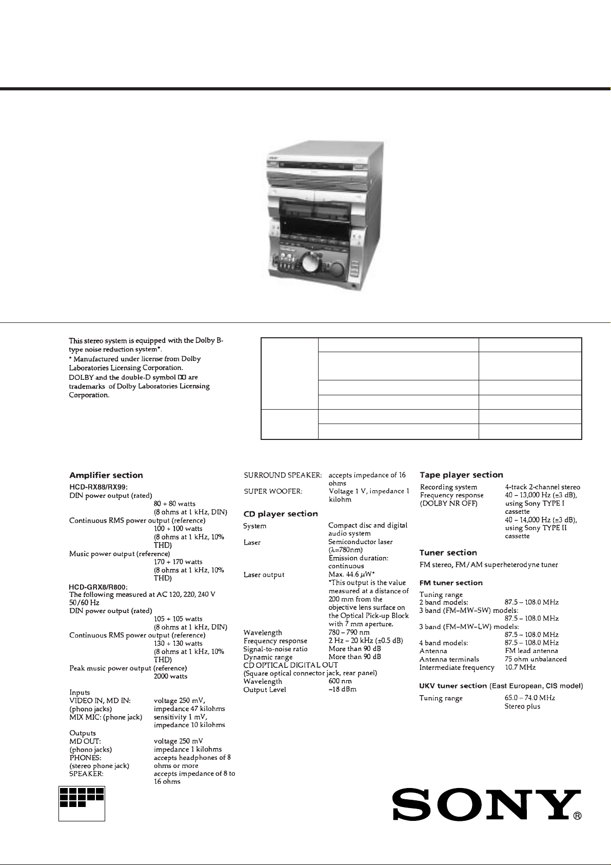
Photo: HCD-GRX8
CD
SECTION
T APE
DECK
SECTION
Model Name Using Similar Mechanism HCD-H991AV
CD Mechanism Type CDM38L-5BD29AL/
Base Unit Type BU-5BD29AL
Optical Pick-up Type KSS-213D/Q-NP
Model Name Using Similar Mechanism NEW
T ape T r ansport Mechanism T ype TCM-230AWR1/230PWR1
AEP Model
UK Model
HCD-RX88/RX99
E Model
HCD-GRX8/R800
Australian Model
HCD-GRX8
CDM38LH-5BD29AL
SPECIFICATIONS
— Continued on next page —
COMPACT DISC DECK RECEIVER
– 1 –
CAUTION
Use of controls or adjustments or performance of procedures
other than those specified herein may result in hazardous radiation exposure.
Notes on chip component replacement
• Never reuse a disconnected chip component.
• Notice that the minus side of a tantalum capacitor may be
damaged by heat.
Flexible Circuit Board Repairing
• Keep the temperature of soldering iron around 270˚C
during repairing.
• Do not touch the soldering iron on the same conductor of the
circuit board (within 3 times).
• Be careful not to apply force on the conductor when soldering
or unsoldering.
Laser component in this product is capable of emitting radiation
exceeding the limit for Class 1.
This appliance is classified as
a CLASS 1 LASER product.
The CLASS 1 LASER PRODUCT MARKING is located on
the rear exterior.
This caution
label is located
inside the unit.
SAFETY-RELATED COMPONENT WARNING !!
COMPONENTS IDENTIFIED BY MARK ! OR DO TTED LINE
WITH MARK ! ON THE SCHEMATIC DIAGRAMS AND IN
THE PARTS LIST ARE CRITICAL TO SAFE OPERATION.
REPLACE THESE COMPONENTS WITH SONY PARTS
WHOSE PART NUMBERS APPEAR AS SHOWN IN THIS
MANUAL OR IN SUPPLEMENTS PUBLISHED BY SONY.
– 2 –
NOTES ON HANDLING THE OPTICAL PICK-UP BLOCK
OR BASE UNIT
The laser diode in the optical pick-up block may suffer electrostatic
break-down because of the potential difference generated by the
charged electrostatic load, etc. on clothing and the human body.
During repair, pay attention to electrostatic break-down and also
use the procedure in the printed matter which is included in the
repain parts.
The flexible board is easily damaged and should be handled with
care.
NOTES ON LASER DIODE EMISSION CHECK
The laser beam on this model is concentrated so as to be focused on
the disc reflective surface by the objective lens in the optical pickup block. Therefore, when checking the laser diode emission, observe from more than 30 cm away from the objective lens.
LASER DIODE AND FOCUS SEARCH OPERATION
CHECK
Carry out the “S curve check” in “CD section adjustment” and check
that the S curve waveform is output three times.
MODEL IDENTIFICATION
— BACK PANEL —
Parts No.
• Abbreviation
G : German model
EE : East European model
MX : Mexican model
HK : Hong Kong model
SP : Singapore model
MY : Malaysia model
TW : Taiwan model
AUS : Australian model
AR : Argentine model
TH : Thailand model
EA3 : Saudi arabia model
EA4 : Israel model
E2 : Without SW tuner E model.
E3 : With SW tuner E model.
PARTS No. MODEL
4-996-817-0
4-996-817-1
4-996-817-2
4-996-817-3
4-996-817-4
4-996-817-5
4-996-817-6
4-996-818-0
4-996-818-1
4-996-818-2
4-996-818-3
4-996-818-4
4-996-818-5
4-997-818-8
4-997-818-9
4-997-720-0
4-997-720-1
4-997-720-2
4-997-720-3
4-997-720-4
4-997-720-5
4-997-720-6
4-997-720-8
4-997-720-9
RX99: AEP, UK, G
RX99: EE, CIS
RX99: AEP, UK, G
RX99: EE, CIS
RX88
RX88
GRX8: TH, EA4
GRX8: E2, E3
GRX8: SP, MY
GRX8: TW
GRX8: HK
GRX8: AUS
GRX8: MX
R800: MX
R800: AR
GRX8: E2, E3
GRX8: SP, MY
GRX8: TW
GRX8: HK
GRX8: AUS
GRX8: MX
GRX8: EA3
R800: MX
R800: AR
PRODUCT
COUNTRY
MALAYSIA
MALAYSIA
INDONESIA
INDONESIA
MALAYSIA
INDONESIA
THAILAND
INDONESIA
INDONESIA
INDONESIA
INDONESIA
INDONESIA
INDONESIA
INDONESIA
INDONESIA
MALAYSIA
MALAYSIA
MALAYSIA
MALAYSIA
MALAYSIA
MALAYSIA
MALAYSIA
MALAYSIA
MALAYSIA
– 3 –

TABLE OF CONTENTS
1. SERVICING NOTE .......................................................... 5
2. GENERAL .......................................................................... 6
3. DISASSEMBLY
3-1. Loading Panel ....................................................................... 8
3-2. Front Panel ........................................................................... 8
3-3. Cassette Mechanism Deck ....................................................9
3-4. Panel Board and Cont Com Board ........................................9
3-5. Disc Tray ........................................................................... 10
4. SERVICE MODE ............................................................11
5. MECHANICAL ADJUSTMENTS ..........................14
6. ELECTRICAL ADJUSTMENTS ............................... 14
7. DIAGRAMS
7-1. Circuit Boards Location ...................................................... 20
7-2. Brock Diagrams
• Tuner Section (AEP, UK, German model)....................... 21
• Tuner Section (East European, CIS model)..................... 23
• CD Section ....................................................................... 25
• Deck Section .................................................................... 27
• Main Section .................................................................... 29
• Power Section ..................................................................31
• Display Section ................................................................ 33
7-3. Printed Wiring Board — CD Section —............................. 37
7-4. Schematic Diagram — CD Section — ............................... 39
7-5. Schematic Diagram
—Tuner (AEP, UK, German model) Section —................. 41
7-6. Printed Wiring Board
—Tuner (AEP, UK, German model) Section —................. 43
7-7. Printed Wiring Board
—Tuner (East European, CIS model) Section — ............... 44
7-8. Schematic Diagram
—Tuner (East European, CIS model) Section — ............... 45
7-9. Schematic Diagram — Deck Section —............................. 47
7-10. Printed Wiring Board — Deck Section — ....................... 49
7-11. Printed Wiring Board — Main Section — ....................... 51
7-12. Schematic Diagram — Main (1/4) Section — ................. 53
7-13. Schematic Diagram — Main (2/4) Section — ................. 55
7-14. Schematic Diagram — Main (3/4) Section — ................. 57
7-15. Schematic Diagram — Main (4/4) Section — ................. 59
7-16. Printed Wiring Board — Mic/HP Section —...................61
7-17. Schematic Diagram — Mic/HP Section — ...................... 62
7-18. Printed Wiring Board — Power Section — ..................... 63
7-19. Schematic Diagram — Power Section — ........................65
7-20. Schematic Diagram — Transformer Section —............... 67
7-21. Printed Wiring Board — Transformer Section — ............ 69
7-22. Printed Wiring Board — Leaf SW Section — ................. 70
7-23. Schematic Diagram — Leaf SW Section — ....................70
7-24. Printed Wiring Board — Display Section — ................... 71
7-25. Schematic Diagram — Display Section — ...................... 73
7-26. Schematic Diagram — Panel Section — ......................... 75
7-27. Printed Wiring Board — Panel Section —....................... 77
7-28. Schematic Diagram — CD Motor Section — .................. 79
7-29. Printed Wiring Board — CD Motor Section —............... 81
7-30. IC Block Diagrams ........................................................... 83
7-31. IC Pin Functions ............................................................... 88
8. EXPLODED VIEWS
8-1. Case Section........................................................................ 98
8-2. Chassis Section ................................................................. 100
8-3. Front Panel Section ........................................................... 101
8-4. CD Mechanism Deck Section-1 (CDM38L-5BD29AL) .. 102
8-5. CD Mechanism Deck Section-2 (CDM38L-5BD29AL) .. 103
8-6. Base Unit Section (BU-5BD29AL) .................................. 104
8-7. TC Mechanism Section 1 (TCM230AWR1) ....................105
8-8. TC Mechanism Section 2 (TCM230AWR2) ....................106
9. ELECTRICAL PARTS LIST ...................................... 107
– 4 –
SECTION 1
SERVICING NOTE
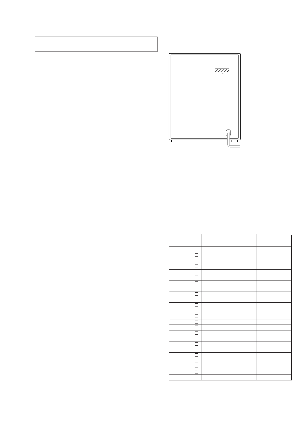
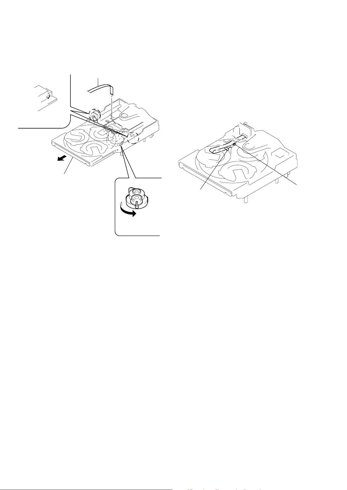
HOW TO OPEN THE DISC TRAY WHEN POWER SWITCH
TURNS OFF
1
Remove the Case.
3
pull-out the disc tray.
2
Turn the cam to the
direction of arrow.
Note for Installation (ROTARY ENCODER)
BU cam
Groove
Note:When attaching the Base unit, Insert the
section A into the groove of BU cam.
Section A
Note:When attaching the BU cam,
engage the Rotary encoder
switch as shown in the figure.
– 5 –
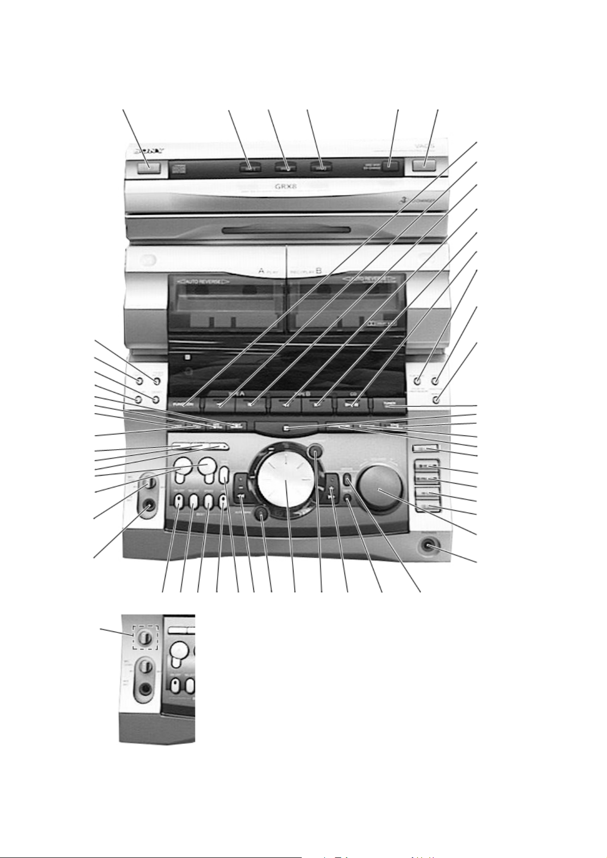
Front Panel
SECTION 2
GENERAL
55
54
53
52
51
50
49
48
47
46
45
44
43
42
1
234 56
7
8
9
10
11
12
13
14
15
16
17
18
19
20
21
22
23
24
25
26
41
40
27
3536373839
3031323334
29
28
– 6 –

LOCATION OF PARTS AND CONTROLS
1 1/u button
2 DISC 1 button
3 DISC 2 button
4 DISC 3 button
5 DISC SKIP/EX-CHANGE button
6 § button
7 FUNCTION button
8 Deck A ª button
9 Deck A · button
10 Deck B ª button
11 Deck B · button
12 CD ·∏ button
13 PLAY MODE/DOLBY NR/TUNER MEMORY button
14 EDIT/DIRECTION button
15 REPEAT/STEREO/MONO button
16 TUNER/BAND button
17 p button
18 MUTING button (RX88)
SONIC FORMATION button (GRX8/RX99/R800)
19 SURROUND button
20 KARAOKE PON/MPX button
21 PTY button (AEP, UK model)
22 r REC button
23 P PAUSE button
24 HI-PUB button
25 CD SYNC button
26 VOLUME knob
27 PHONES jack
28 GROOVE button
29 DBFB button
30 )/+ button
31 ENTER/NEXT button
32 JOG button
33 AUTO BPM
34 0/– button
35 BEAT LEVEL button
36 JAM button
37 SPEED button
38 SELECT button
39 ON/OFF button
40 ECHO LEVEL knob (Saudi Arabia model)
41 MIX MIC jack
42 MIC LEVEL knob
43 PAD A button
44 PAD B button
45 NON STOP button
46 FLASH button
47 LOOP button
48 FILE SELECT button
49 EFFECT button
50 GEQ CONTROL button
51 P FILE MEMORY button
52 DISPLAY button
53 DEMO button
54 CLOCK/TIMER SET button
55 TIMER/SELECT button
– 7 –
SECTION 3
DISASSEMBLY
Note: Follow the disassembly procedure in the numerical order given.
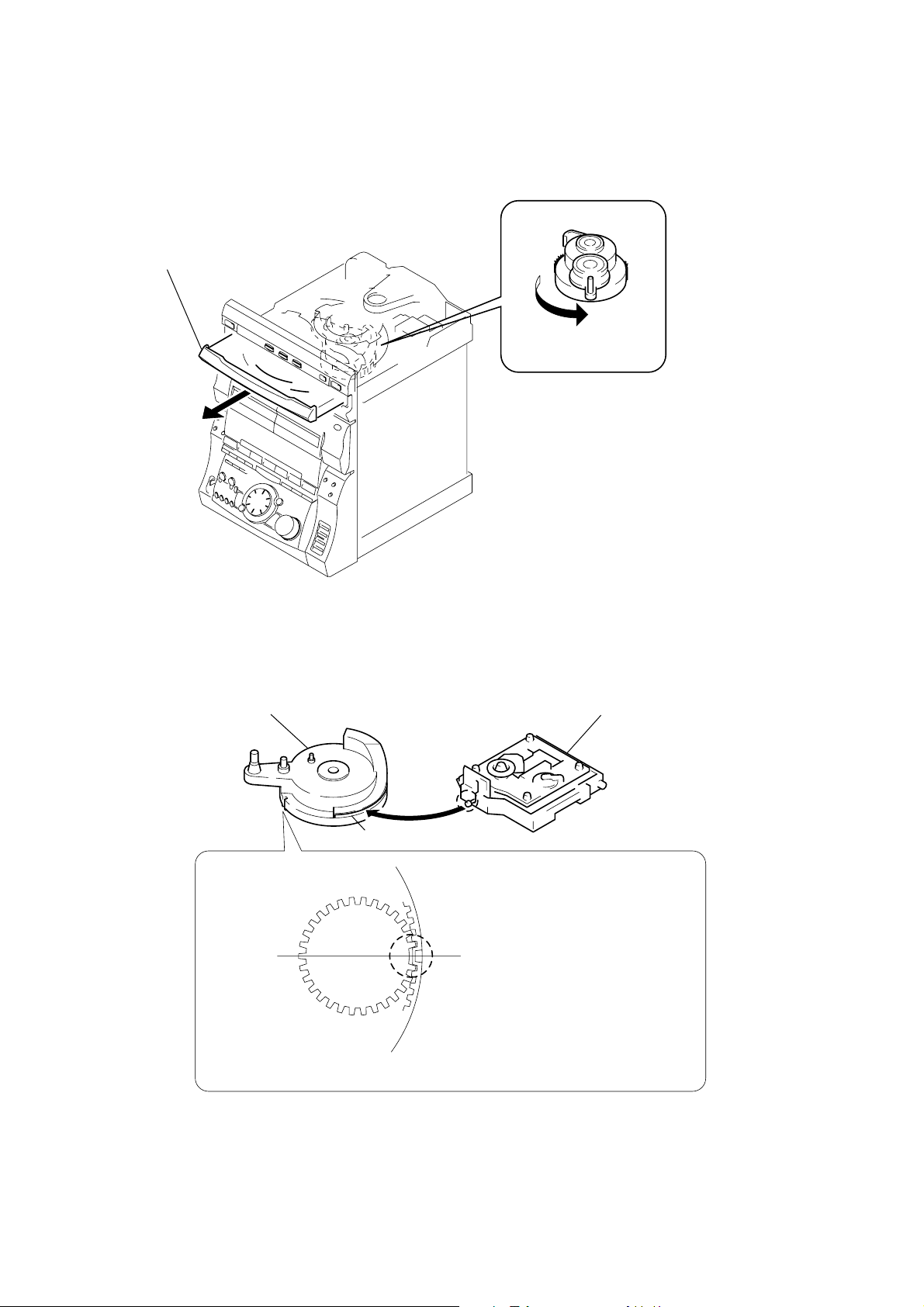
3-1. LOADING PANEL
3
Loading panel
Claws
2
Pull-out the disc tray.
1
Turn the cam to the direction
of arrow.
3-2. FRONT PANEL
3
Screw
(BVTP3x8)
7
(CN106)
8
Flat type wire
(CN101)
4
Connector
(CN203)
Flat type wire
6
Flat type wire
(CN107)
2
Screw
(BVTP3x8)
9
Front panel assembly
1
Three screws
(BVTP3x8)
– 8 –
5
Connector
(CN752)
3-3. CASSETTE MECHANISM DECK
1
Two screws
(BVTT 2x5)
2
Two screws
(BVTT 2x5)
9
Three screws
(BVTP 2.6x8)
!º
Two screws
(BVTP 2.6x8)
!£
Three screws
(BVTP 2.6x8)
!¡
Screw
(BVTP 2.6x8)
!™
Screw
(BVTP 2.6x8)
!¢
Bracket
!∞
Mechanism deck
3
Small damper
4
Small damper
5
Push the cassette lids.
6
Remove the cassette lids.
7
Spring
8
Spring
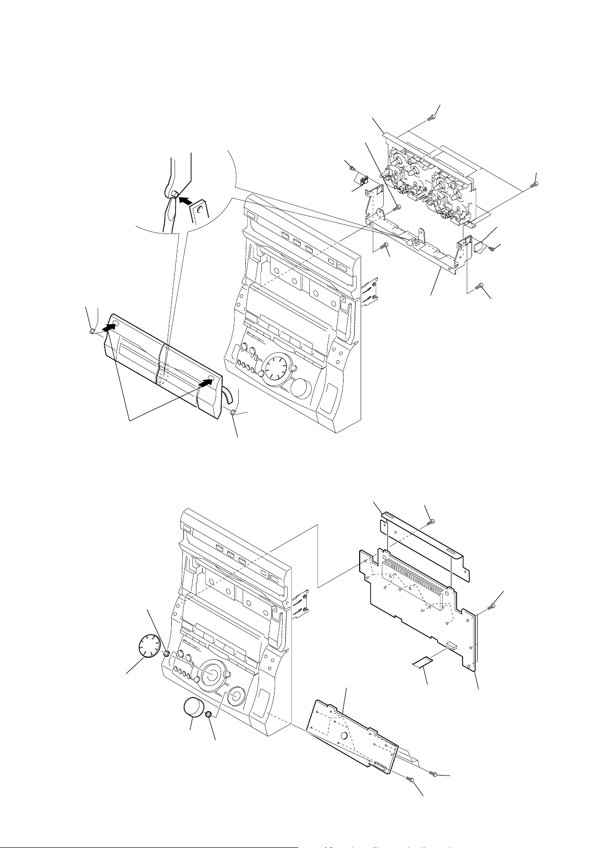
3-4. PANEL BOARD AND CONT COM BOARD
7
6
Konb(Jog)
Nut
8
Konb(Volume)
9
Nut
4
!™ CONT COM
Shield
board
1
Ten screws
(BVTP 2.6x8)
5
Flat type wire
(CN602)
2
Three screws
(BVTP 2.6x8)
3
Panel board
– 9 –
!º
Four screws
(BVTP 2.6x8)
!¡
Six screws
(BVTP 2.6x8)
3-5. DISC TRAY
(Perfom after removing the front panel.)
3
Flat type wire (8 core)
4
Two claws
2
Pull-out the disc tray.
5
Remove the disc tray.
Turn the cam the
1
direction of arrow.
Note: When installing the Disc tray, pull around the flat type wire to
pass through the clawA and clawB, as shown in the figure.
Claw
A
Claw
B
– 10 –

SECTION 4
SERVICE MODE
MC Cold Reset
• The cold reset clears all data including preset data stored in the RAM to initial conditions. Execute this mode when returning the set to the
customer.
Procedure:
1. Press three buttons p , ENTER/NEXT , and 1/u simultaneously.
2. The fluorescent indicator tube becomes blank instantaneously, and the set is reset.
CD Delivery Mode
• This mode moves the pick-up to the position durable to vibration. Use this mode when returning the set to the customer after repair.
Procedure:
1. Press 1/u button to turn the set ON.
2. Press LOOP button and 1/u button simultaneously.
3. A message “LOCK” is displayed on the fluorescent indicator tube, and the CD delivery mode is set.
MC Hot Reset
• This mode resets the set with the preset data kept stored in the memory. The hot reset mode functions same as if the po wer cord is plugged
in and out.
Procedure:
1. Press three buttons p , ENTER/NEXT , and DISC 1 simultaneously.
2. The fluorescent indicator tube becomes blank instantaneously, and the set is reset.
Sled Servo Mode
• This mode can run the CD sled motor freely. Use this mode, for instance, when cleaning the pick-up.
Procedure:
1. Select the function “CD”.
2. Press three buttons p , ENTER/NEXT , and § simultaneously.
3. The Sled Servo mode is selected, if “CD” is blanking on the fluorescent indicator tube.
4. With the CD in stop status, press ) + utton move the pick-up to outside track, or – 0 button to inside track.
5. To exit from this mode, perform as follows:
1) Move the pick-up to the most inside track.
2) Press three buttons in the same manner as step 2.
Note:
• Always move the pick-up to most inside track when exiting from this mode. Otherwise, a disc will not be unloaded.
• Do not run the sled motor excessively, otherwise the gear can be chipped.
Change-over of AM Tuner Step between 9kHz and 10kHz
• A step of AM channels can be changed over between 9kHz and 10kHz.
Procedure:
1. Press 1/u button to turn the set ON.
2. Select the function “TUNER”, and press TUNER/BAND button to select the BAND “AM”.
3. Press 1/u button to turn the set OFF.
4. Press ENTER/NEXT and 1/u buttons simultaneously , and the display of fluorescent indicator tube changes to “AM 9k STEP” or “AM
10k STEP”, and thus the channel step is changed over.
LED and Fluorescent Indicator Tube All Lit, Key Check Mode
Procedure:
1. Press three buttons p , ENTER/NEXT , and DISC 2 simultaneously.
2. LEDs and fluorescent indicator tube are all turned on.
Press DISC 2 button, and the key check mode is activated.
3. In the key check mode, the fluorescent indicator tube displays “K 1 V0 J0”. Each time a button is pressed, “K”v alue increases. Howe ver ,
once a button is pressed, it is no longer taken into account.
“J” Value increases like 1, 2, 3 ... if rotating JOG knob in “+” direction, or it decreases like 0, 9, 8 ... if rotating in “-” direction.
“V” Value increases like 1, 2, 3 ... if rotating VOLUME knob in “+” direction, or it decreases like 0, 9, 8 ... if rotating in “-” direction.
4. To exit from this mode, press three buttons in the same manner as step 1, or disconnect the power cord.
– 11 –
Aging Mode
This mode can be used for checking the operations of the CD player and tape deck.
• When problems occur;
Aging stops, and the stopped state is displayed on the fluorescent display tube.
• When no problems;
Aging continues.
Preparations:
• Set the CD on the DISC1 tray.
• Insert a commercially available tape for recording (tapes which contents can be erased, etc.) in decks A and B.
Setting the aging mode:
Press the p button, ENTER/NEXT button, and DISC SKIP/EX-CHANGE button together.
When the aging mode is set, the CD roulette mark blinks. To exit the mode, press the 1/u button and turn OFF the power.
Sequence:
The aging mode is executed in the following sequence.
If the function is set to “CD” when the aging mode is set, aging is performed starting from the CD player. When set to “T APE A” or “TAPE
B”, aging is started from deck A.
If the function is set to others, aging will not be started until the function is switched to CD or TAPE.
Aging of CD player (12 minutes)
Aging of deck A
Aging of deck B
Maximum about 12 minutes
Display of status:
• The aging status is displayed on the fluorescent display tube.
• Normally, the CD player displays the remaining aging time. But if operations ended abnormally, it displays the cause.
• During the aging of the tape deck, the operations performed will be displayed. If operations ended abnormally , this will be displayed at the
fluorescent display tube.
CD Player
• During normal operations:
Display of fluorescent display tube
**1-@@
**: Displays “CD” and the remaining aging time (minutes) alternately. The remaining aging time is counted down from 12.
@@: Track number being accessed.
• When operations end abnormally:
Display of fluorescent display tube
Display
NO DISC ERR
FOCUS1 ERR
FOCUS2 ERR
GFS ERR
FBIAS ERR
SENSOR ERR
TABLE ERR
TRAY ERR
DISC 1 is NO DISC from the beginning
Focus is not imposed properly
The focus deviated sever al times after the disc rotated normally
GFS ERROR
Error during focus bias adjustment
DISC 1 was found to be NO DISC by the disc sensor
The table did not rotate normally
The tray containing the BD did not operate normally
Main Cause
– 12 –

Tape Deck
Display of Operations
TAPE A AG-1
TAPE A AG-2
TAPE A AG-3
TAPE A AG-4
TAPE A AG-5
TAPE B AG-1
TAPE B AG-2
TAPE B AG-3
TAPE B AG-4
TAPE B AG-5
Operations during aging
• Operations are performed in the following sequence during aging
<CD player>
1. The CD tray rotates and disc 1 is selected.
2. Chucking is performed.
3. TOC is read.
4. Track 1 played back for 2 seconds.
5. The last track is played back for 2 seconds.
6. 1 to 5 is repeated.
7. After 12 minutes of aging, aging is switched to the tape deck.
Operation
TAPE A REW
TAPE A FWD
TAPE A FF
TAPE A REV
TAPE A REW
TAPE B REW
TAPE B FWD
TAPE B FF
TAPE B REV
TAPE B REW
Timing of Ending
Shutoff
2 minute playback
20 seconds or shutoff
2 minutes playback
Shutoff
Shutoff
2 minute playback
20 seconds or shutoff
2 minute playback
Shutoff
<Tape Deck>
1. The tape in deck A is rewound to the head.
2. The FWD side is played back for 2 minutes.
3. The tape is fast forwarded (FF) for 20 seconds. The following procedure is performed w hen the tape end is reached before the 20 seconds.
4. The REV side is played back for 2 minutes.
5. The tape is rewound to the head (REW).
6. The tape in deck B is rewound to the head.
7. The FWD side is played back for 2 minutes.
8. The tape is fast forwarded (FF) for 20 seconds. The following procedure is performed w hen the tape end is reached before the 20 seconds.
9. The REV side is played back for 2 minutes.
10. The tape is rewound to the head (REW).
11. Aging is switched to the CD player.
– 13 –
SECTION 5
)
MECHANICAL ADJUSTMENTS
SECTION 6
ELECTRICAL ADJUSTMENTS
Precaution
1. Clean the following parts with a denatured alcohol-moistened
swab:
record/playback heads pinch rollers
erase head rubber belts
capstan idlers
2. Demagnetize the record/playback head with a head demagne-
tizer.
3. Do not use a magnetized screwdriver for the adjustments.
4. After the adjustments, apply suitable locking compound to the
parts adjusted.
5. The adjustments should be performed with the rated power sup-
ply voltage unless otherwise noted.
Torque Measurement
Mode
FWD
FWD
back tension
REV
REV
back tension
FF/REW
FWD tension
REV tension
Torque meter
CQ-102C
CQ-102C
CQ-102RC
CQ-102RC
CQ-201B
CQ-403A
CQ-403R
Meter reading
31 to 71 g • cm
(0.43 – 0.98 oz • inch)
2 to 6 g • cm
(0.02 – 0.08 oz • inch)
31 to 71 g • cm
(0.43 – 0.98 oz • inch)
2 to 6 g • cm
(0.02 – 0.08 oz • inch)
71 to 143 g • cm
(0.98 – 1.99 oz • inch)
100 g or more
(3.53 oz or more)
100 g or more
(3.53 oz or more)
DECK SECTION 0 dB=0.775V
1. Demagnetize the record/playback head with a head damagnetizer .
2. Do not use a magnetized screwdriver for the adjustments.
3. After the adjustments, apply suitable locking compound to the
parts adjusted.
4. The adjustments should be performed with the rated power supply voltage unless otherwise noted.
5. The adjustments should be performed in the order given in this
service manual. (As a general rule, playback circuit adjustment
should be completed before performing recording circuit adjustment.)
6. The adjustments should be performed for both L-CH and R-CH.
7. Switches and controls should be set as follows unless otherwise
specified.
Signal Used forTape
P-4-A100
WS-48B
P-4-L300
10 kHz, –10 dB
3 kHz, 0 dB
315 Hz, 0 dB
Record/Playback Head Azimuth Adjustment
(Deck A, Deck B)
Note: Perform this adjustments for both decks.
Procedure:
1. Mode : Playback
test tape
P-4-A100
(10kHz, –10dB)
main board
CN301
Pin
1
Pin
3
Azimuth Adjustment
Tape Speed Adjustment
Level Adjustment
(L-CH)
(R-CH)
level meter
set
main board
CN301
Pin
2
(GND
+
–
2. Turn the adjustment screw and check output peaks. If the peaks
do not match for L-CH and R-CH, turn the adjustment screw
so
that outputs match within 1 dB of peak.
L-CH
peak
screw
position
R-CH
peak
output
level
within
1 dB
L-CH
peak
R-CH
peak
within 1dB
screw
position
– 14 –
3. Mode: Playback Tape Speed Adjustment (Deck A)
)
test tape
P-4-A100
(10kHz, –10dB)
set
main board
CN301
Pin
1
(L-CH)
Pin
L
R
2
(GND)
oscilloscope
Note: Set the test mode using the following method and begin tape
speed adjustment.
In the test mode, the speed will switch to double speed or
normal speed each time the HI-DUB button is pressed.
Procedure:
With the power turned ON, press the p button, ENTER/NEXT
button, and DISC 3 button simultaneously.
(The “VOLUME” on the fluorescent display tube will blink while
Pin
3
(R-CH)
in the test mode.)
To exit the test mode, press the 1/u button.
Waveform of oscilloscope
in phase 45
good
°
135
90
°
°
wrong
180
°
4. After the adjustments, apply suitable locking compound to the
parts adjusted.
Adjustment Location: Playback Head (Deck A)
Record/Playback/Erase Head (Deck B)
1
Remove the four claws
2
Window
1. Insert the WS-48B into deck B.
2. Press the · button of deck B.
3. Press the HI-DUB button and play the tape at double speed.
4. Adjust RV1001 of the LEAF SW board so that the reading of
the frequency counter becomes 6000 ± 180 Hz.
5. Press the HI-DUB button and play the tape at normal speed.
6. Adjust RV1002 of the LEAF SW board so that the reading of
the frequency counter becomes 3000 ± 90 Hz.
Adjustment Location: LEAF SW board
Sample Value of Wow and flutter
W.RMS (JIS) less than 0.3%
(test tape: WS-48B)
Playback Level Adjustment (Deck A, Deck B)
Procedure:
Mode: Playback
test tape
P-4-L300
(315Hz, 0dB)
set
main board
CN301
Pin
1
(L-CH)
Pin
3
(R-CH)
level meter
Reverse Foward
Deck A is RV311 (L-CH) and RV411 (R-CH), deck B is RV301
(L-CH) and RV401 (R-CH)
so that adjustment within the following adjustment level.
Adjustment level:
CN301 playback level: 301.5 to 338.3 mV (–8.2 to –7.2 dB)
level difference between the channels: within ± 0.5 dB
Adjustment Location: A UDIO board
Adjustment Location
[LEAF SW BOARD]
RV1001(High Speed)
RV1002(Normal Speed
RV1002
RV1001
– 15 –
Record Bias Adjustment (Deck B)
)
Record Level Adjustment (Deck B)
Procedure:
INTRODUCTION
When set to the test mode performed in Tape Speed Adjustment, when the tape is re wound after recording, the “REC memory
mode” which rewinds only the recorded portion and playback is
set.
This “REC memory mode” is convenient for performing this adjustment. During recording, the input signal FUNCTION will automatically switch to VIDEO.
(After recording, press the – 0 button without stopping will
return to the position where recording was started.)
1. Press FUNCTION button to select VIDEO. (This step is not
necessary if the above test mode has already been set.)
2. Insert a tape into deck B, press the r REC button, and then
press the ( button to start recording.
3. Mode: Record
VIDEO (AUDIO) IN
1) 315 Hz
2) 10 kHz
AF OSC
attenuator
600
Ω
} 50 mV (–23.8 dB)
blank tape
CS-123
set
Procedure:
INTRODUCTION
When set to the test mode performed in Tape Speed Adjustment, when the tape is rewound after recording, the “REC memory
mode” which rewinds only the recorded portion and playback is
set.
This “REC memory mode” is convenient for performing this
adjustment. During recording, the input signal FUNCTION will automatically switch to VIDEO.
(After recording, press the – 0 button without stopping will
return to the position where recording was started.)
1. Press FUNCTION button to select VIDEO. (This step is not
necessary if the above test mode has already been set.)
2. Insert a tape into deck B, press the r REC button, and then
press the ( button to start recording.
3. Mode: Record
VIDEO (AUDIO) IN
315Hz 50 mV (–23.8 dB)
AF OSC
attenuator
600
Ω
set
blank tape
CS-123
4. Mode: Playback
recorded
position
set
main board
CN301
Pin
1
(L-CH)
Pin
3
(R-CH)
level meter
5. Confirm playback the signal recorded in step 2 become adjustment level as follows.
If these levels do not adjustment le vel, adjust the R V341 (L-CH)
and R V441 (R-CH) on the A UDIO board to repeat steps 3 and 4.
Adjustment level: The playback output of 10 kHz le vel difference
against 315 Hz reference should be ± 1.0 dB.
Adjustment Location: A UDIO board
Adjustment Location:
[AUDIO BOARD] (Conductor Side)
RV341(Lch),RV441(Rch)
Record Bias
RV301 RV401
RV441 RV341
RV311(Lch),RV411(Rch)
Playback Level (Deck A)
RV411
RV311
4. Mode: Playback
recorded
position
set
main board
CN301
Pin
1
(L-CH)
Pin
3
(R-CH)
level meter
5. Confirm playback the signal recorded in step 2 become adjustment level as follows.
If these levels do not adjustment level, adjust the R V301 (L-CH)
and RV351 (R-CH) on the MAIN board to repeat steps 3 and 4.
Adjustment level:
CN403 playback level: 47.2 to 53.0 mV (–24.3 to –23.3 dB)
Adjustment Location: MAIN board
[MAIN BOARD] (Conductor Side)
RV301
Record Level (Lch
1 3
CN301
IC301
RV351
Record Level (Rch)
RV301(Lch),RV401(Rch)
Playback Level (Deck B)
– 16 –
TUNER SECTION 0dB=1µV
Note 1: As a front-end (FE1) is dif ficult to r epair if faulty , replace
it with new one.
Note 2: No adjustment is needed due to a tuner pack for except
AEP, UK, German, East European, CIS models.
AM Tuned Level Adjustment
(AEP, UK, German, East European, CIS model only)
Note: FM Tuned Level adjustment should be performed after this
AM Tuned Level Adjustment.
Setting:
Band: MW
loop antenna
(Supplied accessories)
µ
V/m) = SSG output level dB (µV/m) –26dB.
AM RF SSG
30% amplitude
modulation by
400Hz signal
loop antenna
60cm
Field strength dB (
set
AM antenna
terminal (TM1)
Modulation: 999 kHz (at 9 kHz step)
1,050 kHz (at 10 kHz step)
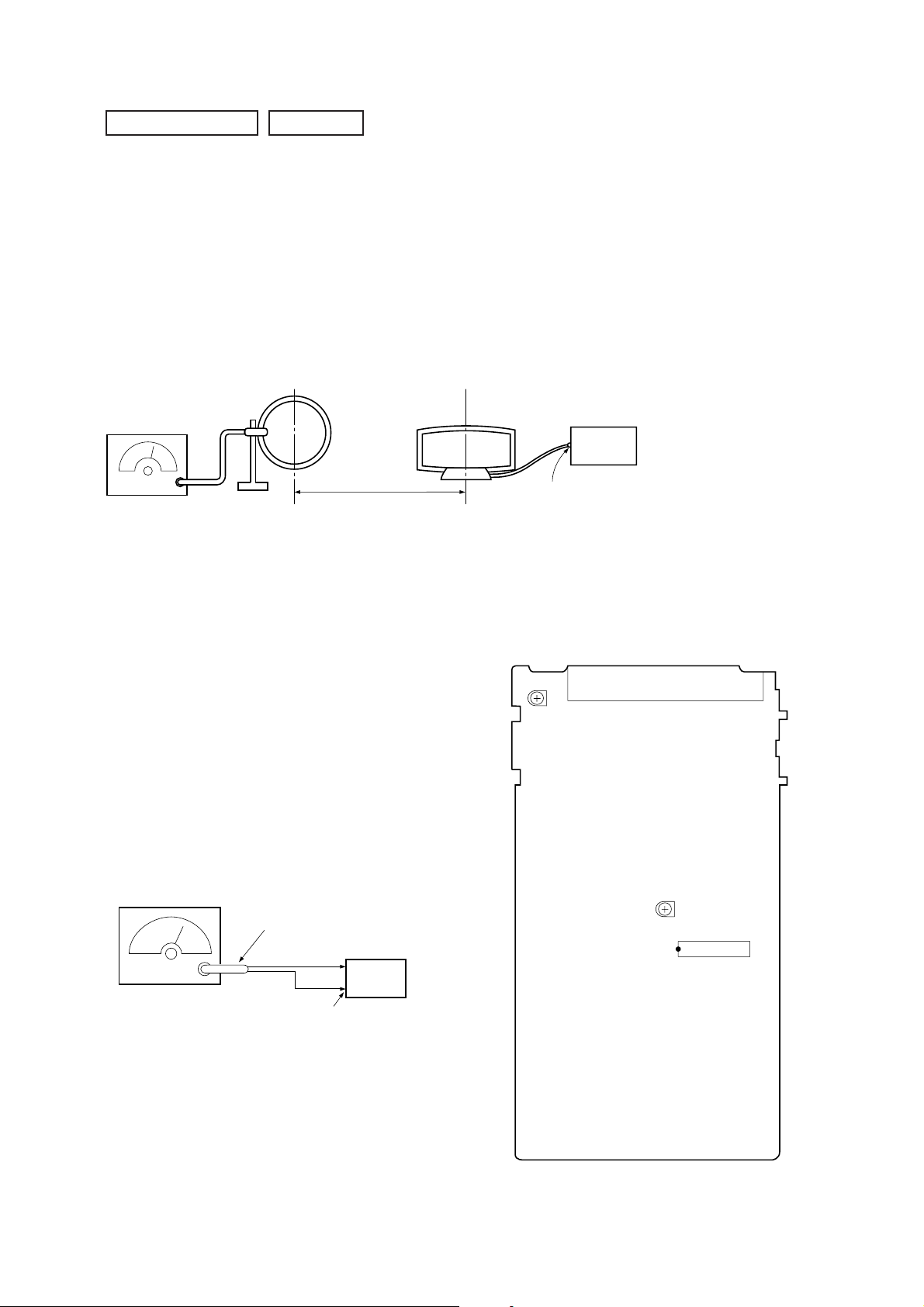
Procedure:
1. Set the output of SSG so that the input level of the set becomes
55 dB.
2. Tune the set to 999 kHz or 1,050 kHz.
3. Adjust RV41 to the point (moment) when the TUNED indicator
will change from going off to going on.
Adjustment Location: TCB board
FM Tuned Level Adjustment
(AEP, UK, German, East European, CIS model only)
Note: This adjustment should be performed after the AM Tuned
Level Adjustment.
Setting:
Band: FM
FM RF SSG
75
Ω
coaxial
set
Carrier frequency: 98MHz
Modulation: AUDIO 1kHz, 75kHz
Output level: 25dB (at 75
deviation (100%)
Ω
FM ANTENNA terminal (TM1)
open)
Adjustment Location
[TCB BOARD] (Component Side)
TM1
RV41
AM Tuner Level
RV42
FM Tuned
Level
IC21
Procedure:
1. Supply a 25 dB 98 MHz signal from the ANTENNA terminal.
2. Tune the set to 98 MHz.
3. Adjust R V42 to the point (moment) when the TUNED indicator
will change from going off to going on.
Adjustment Location: TCB board
– 17 –
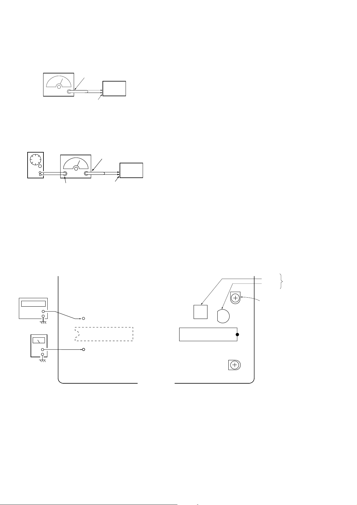
FM Polar Adjustment (East European, CIS model only)
Connection 1 :
FM RF SSG
Carrier frequency: 69 MHz
Output level: 1 mV (60 dB
Modulation: AUDIO 1 kHz, 10 kHz deviation
75
Ω
coaxial
FM antenna
terminal (75
set
Ω
)
µ
) (at 75 Ω open)
Connection 2 :
AF OSC
FM RF SSG
75
Ω
coaxial
set
Procedure :
1. Set the modulation of FM RF SSG to AUDIO 1 kHz, 10 kHz
deviation according to “Connection 1”.
2. Tune the set to 69 MHz.
3. Adjust the RV1702 so that the reading of frequency counter connected to TP1702 (VCO) becomes within 31.25 kHz ± 0.05 kHz.
(VCO adjustment)
4. Then record the reading of the le vel meter connected to TP1701.
5. Set the modula tion of FM RF SSG to AUDIO 31.25 kHz, 10
kHz deviation according to “Connection 2”.
6. Tune the set to 69 MHz.
7. Set the CT1701 to be mechanical center.
8. Adjust the L1701 so that the reading of the level meter connected to TP1701 (FILTER) becomes maximum.
Then adjust the CT1701 so that the reading of the level meter
connected to TP1701 (FIL TER) becomes maximum. (SUB CARRIER PEAK Adjustment)
9. Adjust the RV1701 so that the level at the moment becomes 14
dB higher value than the level recorded in step 4. (SUB CARRIER LEVEL Adjustment)
Audio 31.25 kHz
Carrier frequency: 69 MHz
Output level: 1 mV (60 dB
Modulation: AUDIO 31.25 kHz, 10 kHz deviation
external
modulation
terminal
µ
) (at 75 Ω open)
(EXTERNAL MODULATION)
Adjustment Location: TCB board
Adjustment Location:
[TCB BOARD] (Conductor Side)
frequency counter
TP1701
(FILTER)
level meter
TP1702
(VCO)
IC1701
FM antenna
terminal (75
Ω
)
[TCB BOARD] (Component Side)
L1701
CT1701
RV1701
Sub Carrier
Level
IC1701
RV1702
VCO
Sub Carrier Peak
– 18 –
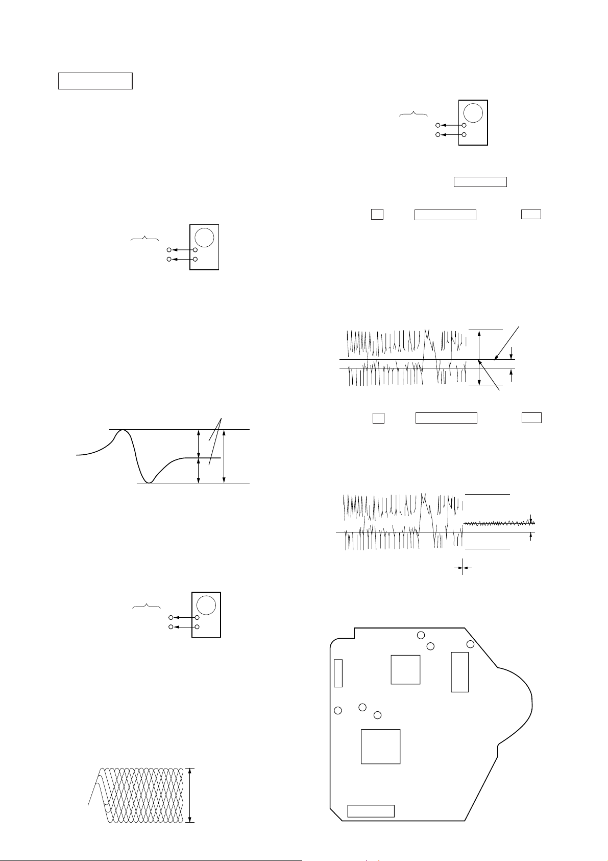
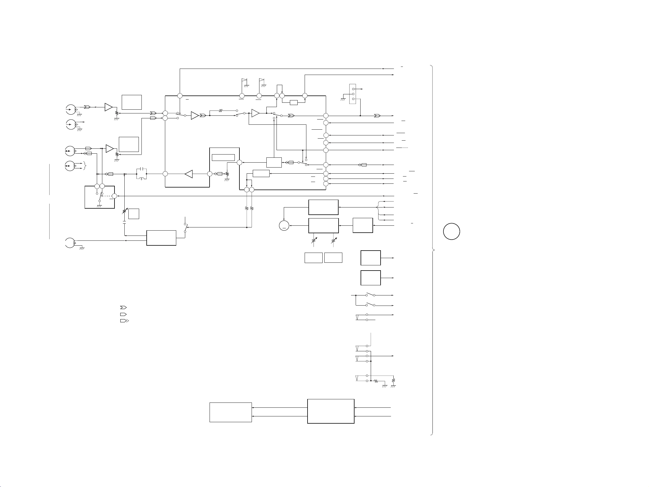
CD SECTION
0V
C (DC
voltage)
Sled servo
OFF
Sled servo
ON
Note:
1. CD Block is basically constructed to operate without adjustment.
Therefore, check each item in order given.
2. Use YEDS-18 disc (3-702-101-01) unless otherwise indicated.
3. Use an oscilloscope with more than 10MΩ impedance.
4. Clean the object lens by an applicator with neutral detergent when
the signal level is low than specified value with the following
checks.
S Curve Check
oscilloscope
BD board
TP (FEO)
TP (VC)
Procedure :
1. Connect oscilloscope to test point TP (FEO).
2. Connect between test point TP (FOK) and Ground by lead wire.
3. Turn Power switch on.
4. Put disc (YEDS-18) in and turned Power switch on again and
actuate the focus search. (actuate the focus search when disc
table is moving in and out.)
5. Check the oscilloscope waveform (S-curve) is symmetrical between A and B. And confirm peak to peak le vel within 3 ± 1Vp-p.
+
–
E-F Balance (Traverse) Check
oscilloscope
BD board
TP (TE)
TP (VC)
+
–
Procedure :
1. Connect oscilloscpe to test point TP (TEO) on BD board.
2. Turned Power switch on. Press FUNCTION button to select
CD.
3. Put disc (YEDS-18) in to play the number five track.
4. Press the p button, ENTER/NEXT button and ^ button
simultaneously several times until the ‘’SHUFFLE” on the
fluorescent display tube blinks.
(The sledding servo is turned OFF.)
5. Check the level B of the oscilliscope’ s w av eform and the A (DC
voltage) of the center of the Traverse waveform.
Confirm the following :
A/B x 100 = less than ± 7%
Traverse waveform
0V
Center of the waveform
B
A (DC voltage)
S-curve waveform
symmetry
A
Within 3
±
1 Vp-p
B
6. After check, remove the lead wire connected in step 2.
Note: • Try to measure several times to make sure than the ratio of
A : B or B : A is more than 10 : 7.
• Tak e sweep time as long as possible and light up the brightness to obtain best waveform.
RF Level Check
oscilloscope
BD board
TP (RF)
TP (VC)
+
–
Procedure :
1. Connect oscilloscope to test point TP (RF) on BD board.
2. Turned Power switch on.
3. Put disc (YEDS-18) in and playback.
4. Confirm that oscilloscope waveform is clear and check RF signal level is correct or not.
Note: Clear RF signal waveform means that the shape “◊” can be
clearly distinguished at the center of the waveform.
RF signal waveform
VOLT/DIV : 200mV
TIME/DIV : 500ns
level : 500 mV ± 100 mVp-p
6. Press the p button, ENTER/NEXT button and ^ button
simultaneously several times until the ‘’SHUFFLE” on the
fluorescent display tube goes off. (The tracking servo and
sledding servo are turned ON.) Confirm the C (DC voltage) is
almost equal to the A (DC voltage) is step 5.
Traverse waveform
Adjustment Location :
[ BD BOARD ] — SIDE A —
CN101
TP
(GND)
TP (RF)
IC101
TP
(TEO)
TP
(FEO)
IC103
TP
(VC)
TP
(FOK)
IC102
level : 1.3 ± 0.3 Vp-p
IC102
– 19 –
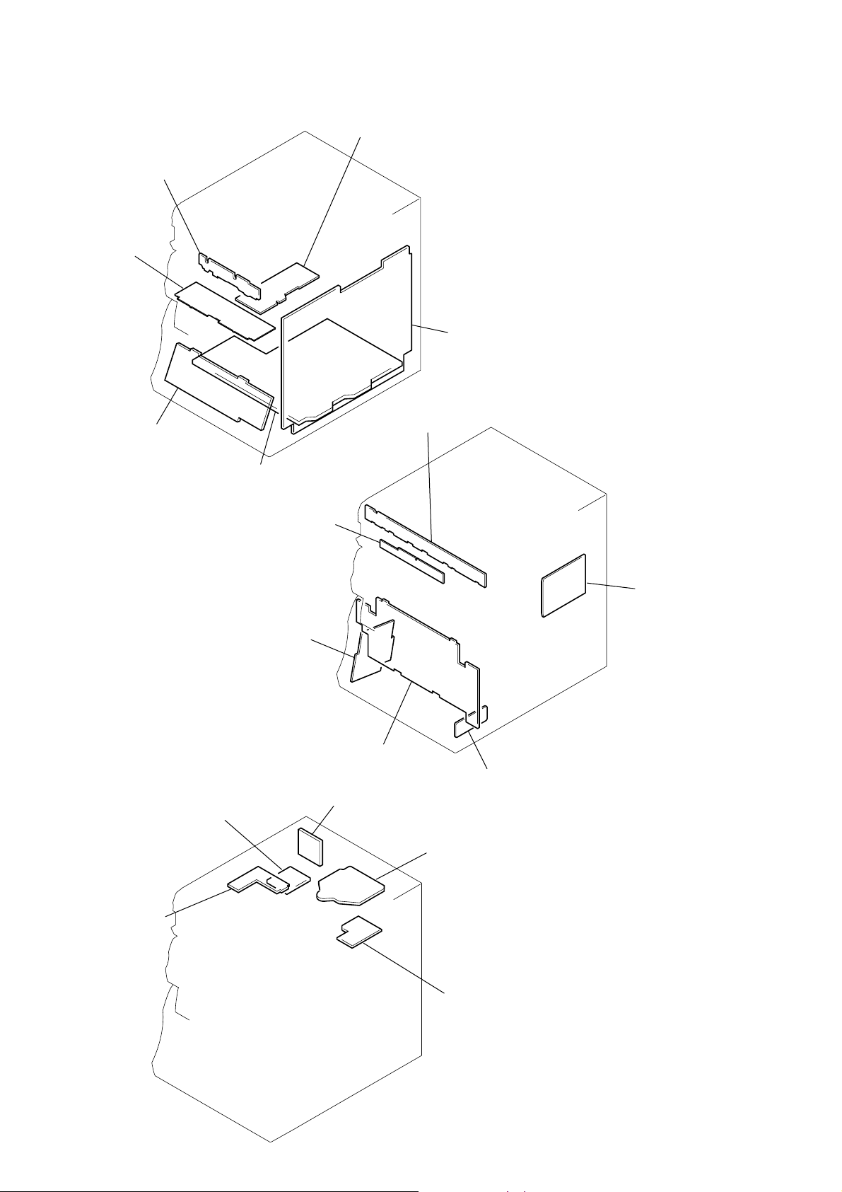
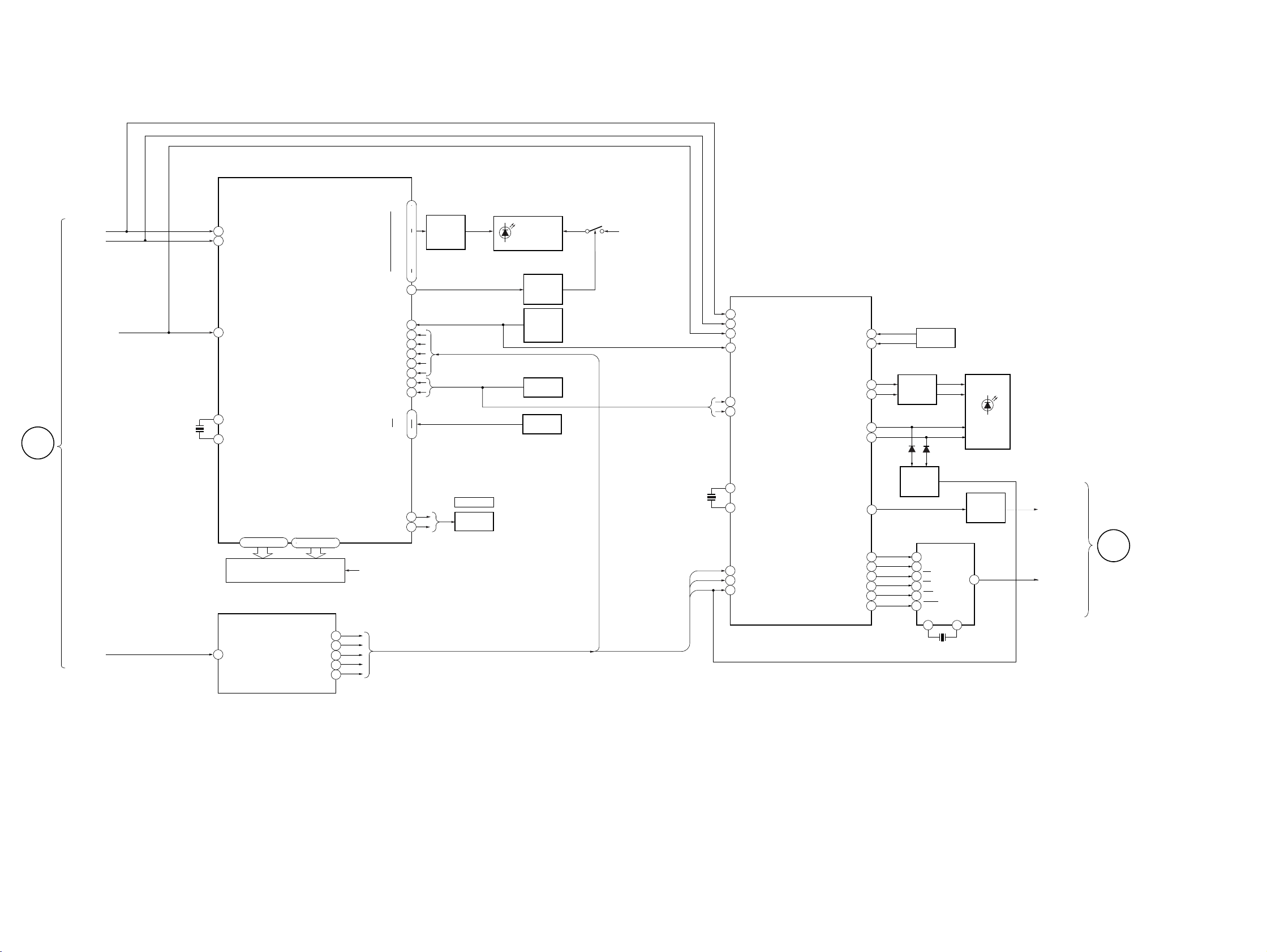
7-1. CIRCUIT BOARDS LOCATION
d
d
CD-SW board
MIC board
PANEL board
HP board
ENCAPSULATED
COMPONENT (GRX8/R800)
TCB board (RX88/RX99)
DECO board
LEAF SW board
AUDIO board
CONT COM board
SECTION 7
DIAGRAMS
TRANSFORMER board
MAIN boar
CONNECTOR board
POWER board
MOTOR (TURN) board
BD board
SENSOR board
MOTOR (SLIDE) boar
– 20 –
HCD-GRX8/R800/RX88/RX99
7-2. BLOCK DIAGRAMS
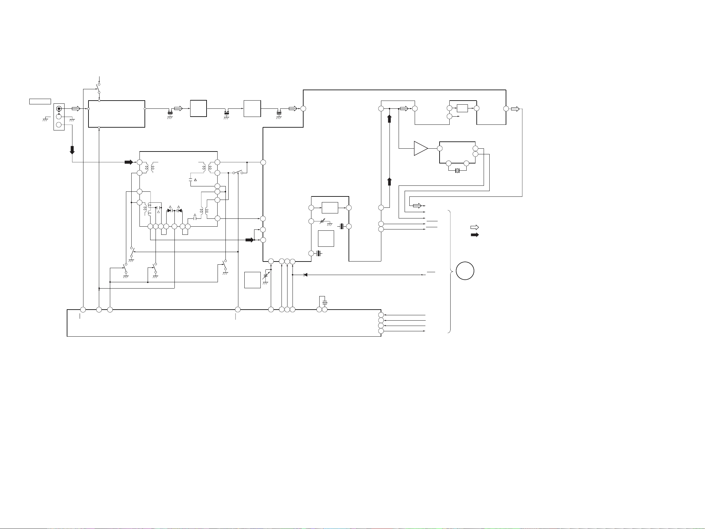
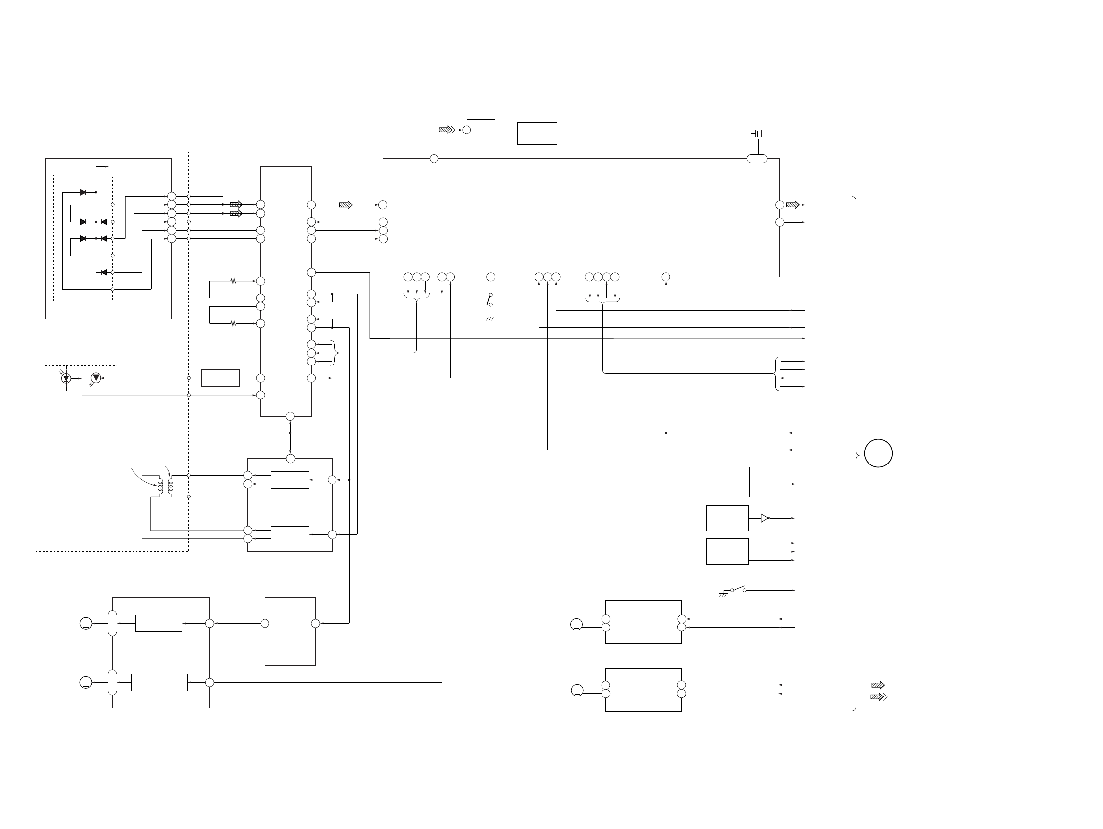
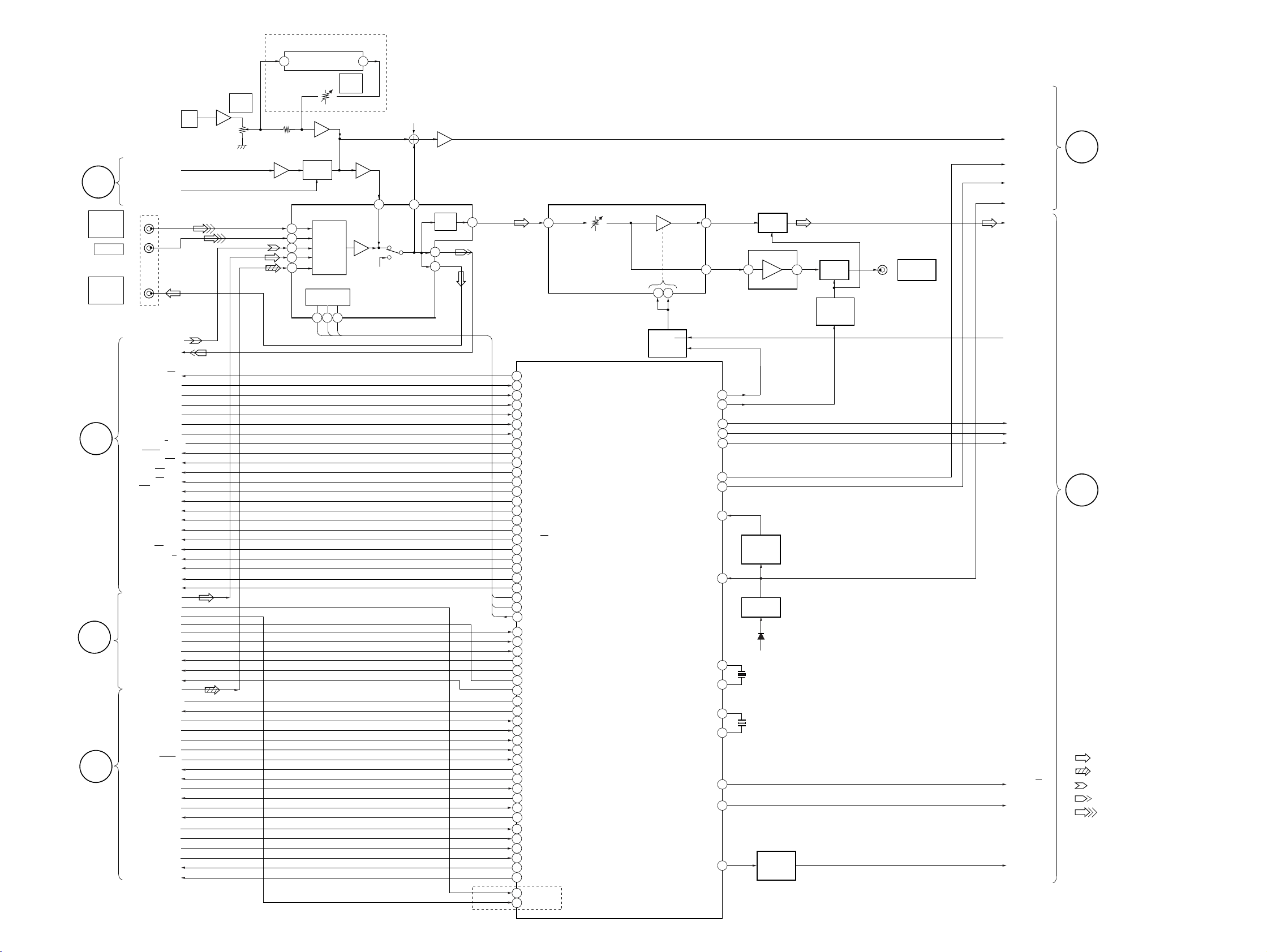
– TUNER SECTION – (AEP, UK, German model)
ST +10V
TM1
ANTENNA
FM 75Ω
COAXIAL
AM
Q5
ANT IN
VT
FE1
FM FRONT END
IF OUT
LW SW
Q13
MW
SW
6
5
3
2
26 25 24 23 22 21
Q14
CF1
10.7MHz
FE2
MW/LW FRONTEND
Q12
MW
SW
28
29
26
27
10.7MHz
REG
AM OSC
FM AFC
AM RF IN
FM SD
OSC.BUFF
30 14
CF3
ADJ
VCO STOP
AM/FM
15
13
AM MIX
MUTE
IF BUFF
1 FM IN
FM/AM MPX
IC41
2
AM
12
SD
ADJ
AM
10
SD
450kHz
D41
RV41
X42
AM IF
AM
TUNED
LEVEL
IFT41
X41
10.7MHz
4
9
FM DET OUT
AM IF
FM
DET
23 22
AM
24
DET
OUT
7
STEREO
6
TUNED
OUT L
MPX IN
OUT R
IC1751
57
4
ST L
RDS INT
RDS DATA
STEREO
TUNED
MUTE
21
LPF
RCH
20
RDS DECODER
IC1752
13 14
X1751
4.332MHz
A
MAIN
SECTION
AMP IN L
AMP
OUT
17
L
19
2
16
• R CH: Same as L ch
• SIGNAL PATH
: FM
: MW
CF2
IF AMP
Q1, 2
20
10.7MHz
12
13
14
15
16
17
LW SW
Q11
MW
SW
IF AMP
Q3, 4
Q9
RV42
FM
TUNED
LEVEL
(Page 29)
X21
2
AM OSC
7
FM
1214
FM/AM IF
VCO STOP
1710
9
FM
VT1
MW
09
PLL
IC21
11
MW
1 24
XIN
4.5MHz
XOUT
3 ST-CE
CE
4
DI
5
CL
DO
6
COM-DIN
COM-CLK
COM-DATA
– 21 – – 22 –
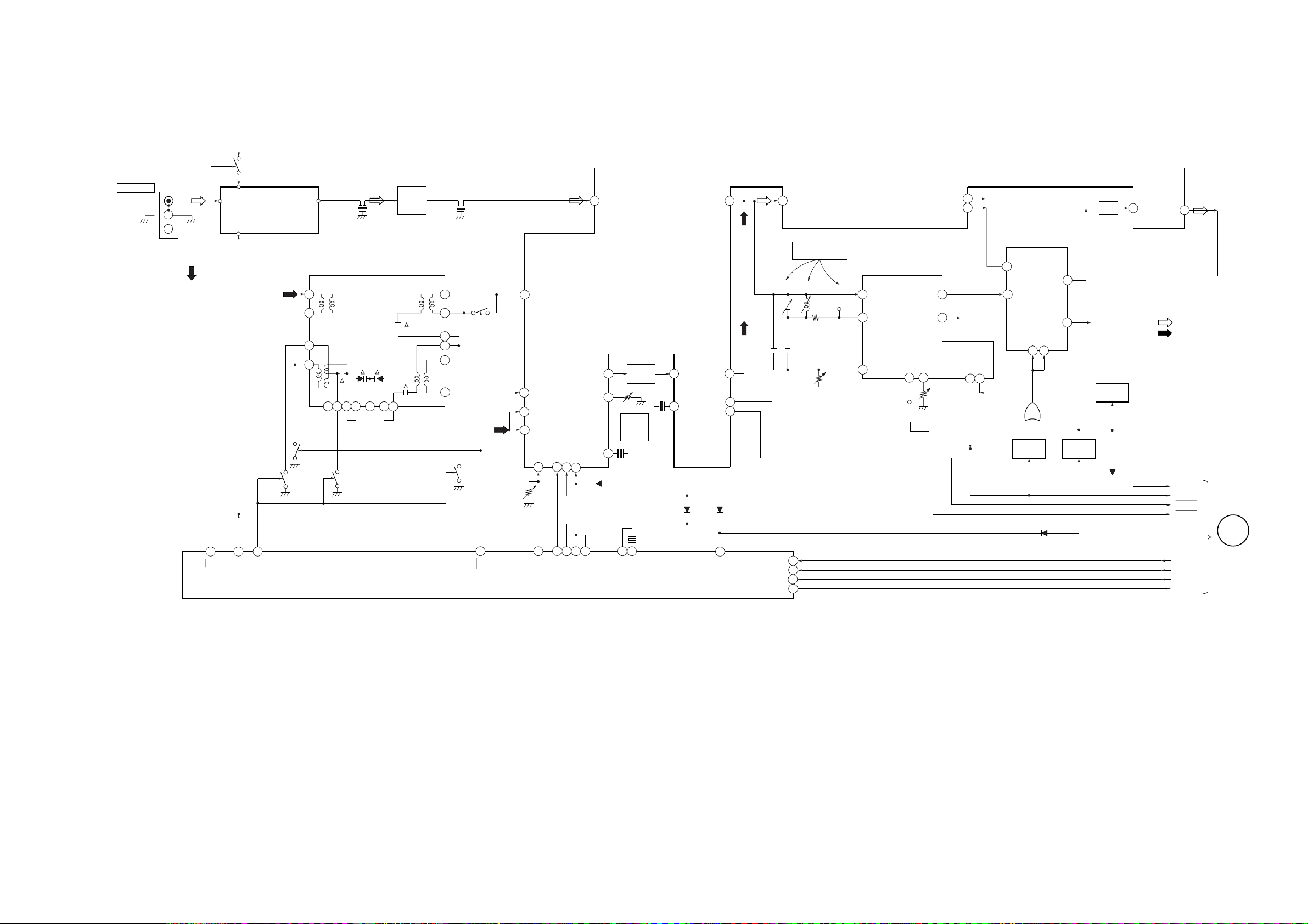
– TUNER SECTION – (East European, CIS model)
22
MPX IN
21
OUT L
LPF 19
AMP
IN
L
AMP
OUT
L
17
4
5
3
6
ST-CE
COM-DIN
COM-CLK
COM-DATA
A
MAIN
SECTION
CE
DI
CL
DO
• R CH: Same as L ch
• SIGNAL PATH
: FM
: MW
D42 D43
13
FM LOW
SUB CARRIER
PEAK
L1701CT1701
TP1701
2
3
20
RV1701
SUB CARRIER
LEVEL
7
6
910
POLAR
DECODER
IC1701
IN
POUT
L OUT
R OUT
SUB IN
MON
VCO
ST IND
VCO
STOP
18 17
R CH
13
12
POLAR/PILOT
SWITCH
IC1702
14
9 11
L IN
L OUT
CA
R OUT
4
R CH
SWITCH
Q1701
SWITCH
Q1702
SWITCH
Q1703
D1704
D1703
D1701
D1702
ST-L
STEREO
TUNED
MUTE
TP1702
RV1702
VCO
(Page 29)
TM1
AM
ANTENNA
FM 75Ω
COAXIAL
ANT IN
ST +10V
Q5
VT
FE1
FM FRONT END
IF OUT
CF1
10.7MHz
IF AMP
Q1-4
CF3
10.7MHz
1 FM IN
REG
FM/AM MPX
IC41
1710
09
PLL
IC21
11
FM
TUNED
LEVEL
15
13
30 14
RV42
2
1214
7
8
10
X42
450kHz
D41
AM/FM
VCO STOP
IF BUFF
MUTE
AM
SD
AM
TUNED
LEVEL
12
RV41
2
AM IF
IFT41
4
9
AM IF
FM
DET
STEREO
TUNED
7
6
X41
10.7MHz
1 24
X21
4.5MHz
AM MIX
AM
SD
6
28
5
2
15
17
16
14
12
13
29
26 25 24 23 22 21
20
9
LW SW
Q9
27
FE2
MW/LW FRONTEND
Q11
MW
SW
Q12
MW
SW
Q14
LW SW
Q13
MW
SW
AM OSC
AM RF IN
FM
VT1
MW
MW
AM OSC
FM
VCO STOP
FM/AM IF
IF REQ
XIN
XOUT
3
OUT R
RCH
20
ADJ
FM SD
ADJ
OSC.BUFF
FM AFC
26
23
FM DET OUT
24
AM
DET
OUT
POLA
L IN
HCD-GRX8/R800/RX88/RX99
– 23 – – 24 –
HCD-GRX8/R800/RX88/RX99
– CD SECTION –
OPTICAL PICK-UP BLOCK
B+
K
E
A
D
A
B
D
C
C
B
F
1
4
2
5
10
6
LASER
DIODE
DETECTOR
LD DRIVE
Q101
FOCUS/TRACKING SERVO.
RF AMP
IC101 (1/2)
38
PD1
RF O
SENS1
SENS2
XRST
23
LOCK
C.OUT
FE O
FE M
TA M
TA O
DATA
XLT
CLK
FOK
33
19
24
25
26
12
13
22
21
20
27
39
41
42
2
1
45
47
3637LD
PD2
F
E
FEI
FEO
TEO
TEI
PD
IC391
1
D.OUT
71
DOUT
RF
44
LOCK
29
14
CNIN
15
SEIN
DATAO
CLKO
XLTO
15 16 17
6
7
FOK
MDP
23
27
SPOD
21
CD DIGITAL
OUT
OPTICAL
DIGITAL SIGNAL PROCESSOR
S101
LIMIT
IC103
DATA
10 11 12 75
XLAT
CLOK
SQCK
SENS
SCOR
SQSO
8
79 100
XRST
89 • 90
XTAI
LOUT1
LOUT2
16.9344MHz
•
XTAO
X101
86
93
L-CH
R-CH
CD CLK
CD DATA
SENS2
SCOR
SQ DATA
SQ CLK
SENS
M102
SLED MOTOR
M101
SPINDLE
MOTOR
09
XRST
TRACKING
FOCUS
COIL
11
M
•
12
13
M
•
14
COIL
2-AXIS
DEVICE
SLED/SPINDLE
MOTOR DRIVE
IC102 (2/2)
SLED MOTOR
DRIVE
SPINDLE MOTOR
DRIVE
T+
–
T
–
F
F+
6
3
15
16
18
17
9
MUTE
TRACKING
COIL DRIVE
FOCUS/TRACKING
COIL DRIVE
IC102 (1/2)
FOCUS
COIL DRIVE
SLED
SERVO
IC101 (2/2)
SL P
SL O
S801
DET
TABLE
SENSOR
IC702
DISC
SENSOR
IC703
ROTARY
ENCODER
S811
Q701
27
26
TURN
MOTOR DRIVER
IC701
M701
1416
TURN
MOTOR
M801
SLIDE
MOTOR
M
M
7
2
4
7
OUT1
OUT2
MOTOR DRIVER
OUT2
OUT1
SLIDE
IC801
IN1
IN2
RIN
FIN
OPEN/CLOSE
3
6
2
10
XLAT
T. SENS
DISC SENS
ENC 1
ENC 2
ENC 3
OPEN
TBL.L
TBL.R
LOAD IN
LOAD OUT
C
MAIN
SECTION
(Page 29)
• R CH: Same as L ch
• SIGNAL PATH
: CD
: Digital out
– 25 –
– 26 –
– DECK SECTION –
HCD-GRX8/R800/RX88/RX99
HP101
PB HEAD
(DECK A)
REC/PB HEAD
(DECK B)
HRPE101
ERASE HEAD
PB A/B
MS OUT
PB L
LM ON/OFF
NORM/HIGH
NR ON/OFF
REC/PB/PASS
REC L
BIAS ON/OFF
RM ON/OFF
ALC ON/OFF
RELAY REC/PB
CAPM CNT1M
CAPM CNT2M
CAPM CNT1P
CAPM CNT2P
CAP M H / L
A SHUT
B
MAIN
SECTION
(Page 29)
17
2
DOLBY NR
RECOUT
C
32 33
S1008
B CrO
19
B 120/70
PAS
BIAS SW
M
2
DOL
DOLBY
TYPE B
M1
CAPSTAN
MOTOR
CN301
3
R CH
28
27
M
MS
26
PB OUT
LM ON/
OFF
NORM/
HIGH
NR ON/
OFF
PB
RIN
BIAS ON/OFF
RM ON/OFF
ALC ON/OFF
CAP MOTOR
CONTROL
Q336-343
CONTROL
RV1002
NORMAL
SPEED
SPEED
Q1001
40
25
18
23
24
44
20
22
15
RV1001
HIGH
SPEED
1
SWITCH
Q335
REEL
DETECT
IC1001
S1004
A CrO
RV311
4
PLAYBACK
LEVEL
DECK A
RV301
PLAYBACK
LEVEL
DECK B
RV341
REC
BIAS
REC BIAS
BIAS OSC
T621, Q621, 622
IC611
L
R
L
R
X
R CH
R CH
3
P
ERASE BIAS
IC601
1
IC602
R
REC/PB
16
PB-A/B
A IN
48
B IN
46
RV301
REC LEVEL
+7.5V
Q623
EQIN
38
EQOUT
36
A 120/70
70
120
DOLBY NR
IC301
39
REEL
DETECT
IC1002
S1001 (A PLAY)
• R CH : Same as L ch
• SIGNAL PATH
+5V
S1002 (B PLAY)
: PB (DECK A)
: PB (DECK B)
: REC (DECK B)
09
• PLUNGER SOLENOID is supplied
as the MECHANICAL BLOCK ASSY.
A DECK/
B DECK
PLUNGER
TRIGGER
MOTOR
CONTROL
Q331-334
S1003
(A HALF)
S1005
(REC A)
S1006
(B HALF)
S1009
(REC B)
+5V
+5V
B SHUT
A PLAY
B PLAY
B HALF
B TRIG
A TRIG
– 27 – – 28 –
HCD-GRX8/R800/RX88/RX99
– MAIN SECTION –
J751
MIX
MIC
(Page 34)
DISPLAY
SECTION
F
VIDEO/IN
(AUDIO)
L
MD IN L
MD/VIDEO
(AUDIO)
OUT L
DJ-SIG
DJ-MUTE
J101
PB L
REC L
IC750(1/2)
RV750
MIC
LEVEL
GRX8:EA3
ECHO PROCESSOR
IC751
29
LPF 1 IN LPF 2 OUT
ECHO
LEVEL
R-CH
IC750(2/2)
Q411
SELECT
SWITCH
MICON
INTERFACE
34
33 32
1 2 3
IC411(2/2)
7
60 2
R-CH
IC411(1/2)
36
MUTE
1
V
64
MD
69
TC
67
TU
66
CD
68
MIX AMP
IC401
6
7
EQ
IC111(1/2)
EQ
42
AMP
58
57
VOLUME
IC111(2/2)
41 36
38 39
DBFB
SWITCH
Q111,112
SPE SIG
E
IIC DATA
IIC CLK
RESET
MUTE
Q113
J191
MUTE
40
6
SUPER WOOFER
AMP
IC191
1
Q191
DBFB
SWITCH
Q141,143
SUPER
WOOFER
FRONT
DBFB
DISPLAY
SECTION
(Page 33)
B
DECK
SECTION
(Page 28)
A
TUNER
SECTION
(Page 22, 24)
C
CD
SECTION
(Page 26)
09
RELAY REC/PB
A SHUT
B SHUT
B HALF
A HALF
A PLAY
B PLAY
PB A / B
NORM/HIGH
BIAS ON/OFF
RM ON/OFF
NR ON/OFF
REC/PB PASS
CAPM CNT1M
CAPM CNT2M
CAPM CNT1P
CAPM CNT2P
ALC ON/OFF
LM ON/OFF
CAP M H/L
A TRG
B TRG
MS OUT
ST L
RDS DATA
RDS INT
COM DIN
COM DATA
STEREO
TUNED
ST CE
MUTE
COM CLK
L CH
TBL. L
TBL. R
SCOR
T. SENS
SENS 2
SENS
X RST
CD CLK
CD DATA
DISC SENS
SQ CLK
SQ DATA
X LAT
OPEN
ENC-1
ENC-2
ENC-3
LOAD IN
LOAD OUT
97
TC RELAY
26
A SHUT
27
B SHUT
28
B HALF
98
A HALF
95
A PLAY SW
96
B PLAY SW
87
PB A/B
93
EQ H//N
BIAS
92
90
REC MUTE
89
NR ON/OFF
R/P PASS
88
CAPM CNT1M
85
CAPM CNT2M
86
17
CAPM CNT1P
CAPM CNT2P
77
99
ALC ON/OFF
TC MUTE
87
82
CAP M H/L
83
A TRG
84
B TRG
31
AMS IN
1
3
M62442 LAT
2
52
M62442 DATA
3
51
M62442 CLK
66
ST DIN
70
STEREO
TUNED
69
68
ST CE
72
ST MUTE
67
ST DOUT
ST CLK
65
60
TBL L
61
TBL R
SCOR
18
76
T SENS
73
SENS 2
74
SENS
57
XRST
48
CD CLK
47
CD DATA
75
DISC SENS
36
SQ CLK
34
SQ DATA IN
58
XLT
OUT OPEN
81
ENC1
80
ENC2
79
ENC3
78
LOAD IN
64
LOAD OUT
63
22
RDS DATA
RDS INT
21
RX88/RX99:
AEP,UK,G
MASTER CONTROL
IC501
PL RELAY
POWER
CD POWER
STK MUTE
DBFB H/L
TA MUTE
F RELAY
R RELAY
IIC DATA
IIC CLK
RESET
AC CUT
XT1
XT2
2
1
6
7
8
55
56
F RELAY
R RELAY
PL RELAY
D
15
RESET
SWITCH
Q951
16
RESET
IC951
D951
X1
11
10
X2
14
13
46
100
+5V
X501
5MHz
X502
32.768KHz
5
MUTE
SWITCH
Q142
POWER ON/OFF
CD POWER
STK MUTE
POWER
SECTION
(Page 31)
• R CH: Same as L ch
• SIGNAL PATH
: FM
: CD
: PB
: REC
: VIDEO/MD
• Abbreviation
G : German model.
EA3 : Saudi Arabia model.
– 29 – – 30 –
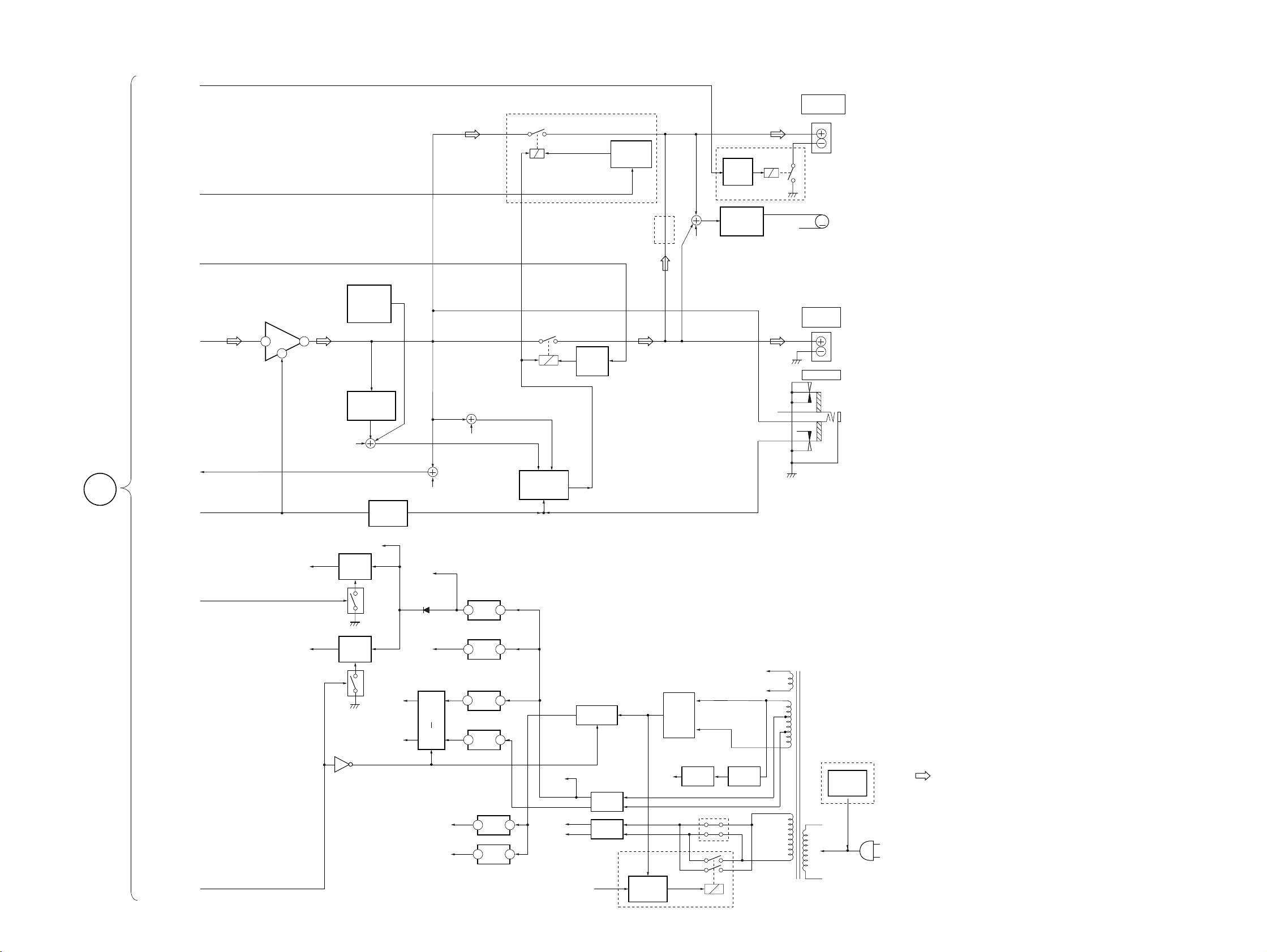
– POWER SECTION –
HCD-GRX8/R800/RX88/RX99
PL RELAY
R RELAY
F RELAY
FRONT
FRONT
POWER AMP
IC201
3 12
8
THERMAL
DET
Q321,322
THP321
OVER LOAD
DET
Q201
GRX/R800/RX99
RY402
RY401
RELAY
DRIVE
Q401,402
RELAY
DRIVE
Q403,407
RX88
Rch
RELAY
DRIVE
Q408
FAN MOTOR
DRIVER
Q961, 962
RY404
FRONT
Rch
UNREG
–12V
TM402
SURROUND
SPEAKER
GRX8/R800/RX99
M901
M
FAN
MOTOR
TM401
FRONT
SPEAKER
J755
PHONES
D
MAIN
SECTION
(Page 30)
09
DBFB
STK MUTE
CD POWER
POWER ON/OFF
CD+5V
AU/D5V SW
Rch
D5V
SWITCHED
CD REG
Q931
+5V REG
Q933
Q937
– 31 –
Q932
Q934
MUTE
SWITCH
Q304,305
A+7V
A–7V
+5.6V
D932
M+7V
SWITCH
Q901
Q905
Rch
+10V
ST+10V
Rch
+5.6V REG
IC931
3 1
+7V REG
IC941
3 1
+7V REG
IC901
3
–7V REG
IC902
3
+10V REG
IC911
3 1
3 1
+10V REG
IC921
PROTECT
CONTROL
Q306,307
T501
POWER
TRANSFORMER
VF
RECT
D111,112
VF
GRX8:E2,E3,SP,MY,HK,TW,EA3
/R800:AR
VOLTAGE
SELECTOR
S501
• R CH : Same as L ch
• SIGNAL PATH
: FM
• Abbreviation
: Without SW tuner E model.
E2
: Without SW tuner E model.
E3
: Saudi Arabia model.
EA3
: Singapore model.
SP
AC
IN
: Malaysia model.
MY
: Hong Kong model.
HK
: Taiwan model.
TW
:Argentine model.
AR
1
2
UNREG
–12V
POWER B+
POWER B–
+12V REG
Q911-913
+7V
RECT
D102
RECT
D101
DRIVER
RX88/RX99
RELAY
Q101
VFDP
RECT
D103,
D104
VF REG
Q111
GRX8/R800
RY101
– 32 –
HCD-GRX8/R800/RX88/RX99
– DISPLAY SECTION –
IIC DATA
IIC CLK
RESET
X601
8MHz
E
MAIN
SECTION
(Page 30)
SPE SIG
SDA
24
SCL
23
10
RESET
XOUT
8
XIN
9
SEG1-SEG20
FL601,Q70,702
FLUORESCENT INDICATOR TUBE
SPEANA BPF FILTER
IC603
4
LINE IN
DISPLAY CONTROL
IC601
GR1-GR13
41 - 5354 - 57
F01
F02
F03
F04
L+R
79
LED1
•
80
•
1
LED
SWITCH
6
•
11
•
12
•
14
18
LED15
L SEL
SIRCS
L+R
JOG A
JOG B
KEY 0
KEY 3
VOL A
VOL B
25
33
34
35
36
37
32
21
22
26
29
S602
VOLUME
19
20
ROTARY
ENCODER
SPEANA 1
SPEANA 2
SPEANA 3
SPEANA 4
VF
SP1
17
SP2
16
SP3
15
SP4
14
L+R
13
PANEL LED
LED
CONTROL
Q603
REMOTE
CONTROL
RECEIVER
IC602
S601
(JOG)
ROTARY
ENCODER
KEY
MATRIX
Q601,602
D+5V
X501
8MHz
SP1
SP4
L+R
19
I2C DATA
I2C CLK
18
RESET
4
29
SIRCS
27
JOG A
28
JOG B
2
XOUT
XIN
3
33
BPF LOW
36
BPF HIGHT
37
L+R
PANEL CONTROL
IC801
KEY O
KEY 1
BPM LED B
BPM LED A
BOMBER LED
ON/OFF LED
MUTE
DATA
CLK
LAT
CH
RST
BSY
D805
S801-808
KEY
MATRIX
LED
SWITCH
Q854,855
SPEANA
CONTROL
Q958-960
SOUND MIX
SD
15
SI
14
ST
8
CH
16
RST
17
BUSY
20
XT XT
23
4.09MHz
D806
IC851
X851
OUT
D801-803
PANEL LED
MUTE
SWITCH
Q851
23
DJ MUTE
DJ SIG
F
MAIN
SECTION
(Page 29)
38
39
61
62
63
64
5
14
15
16
13
12
20
09
– 33 – – 34 –
THIS NOTE IS COMMON FOR PRINTED WIRING
50mV/DIV, 1msec/DIV
0.2Vp-p
135µsec
5Vp-p
135µsec
5Vp-p
BOARDS AND SCHEMATIC DIAGRAMS.
(In addition to this, the necessary note is printed
in each block.)
For schematic diagrams.
Note:
• All capacitors are in µF unless otherwise noted. pF: µµF
50 WV or less are not indicated except for electrolytics
and tantalums.
• All resistors are in Ω and 1/
specified.
¢
•
: internal component.
4
W or less unless otherwise
• C : panel designation.
Note: The components identified by mark ! or dotted line
with mark ! are critical for safety.
Replace only with part number specified.
• U : B+ Line.
• V : B– Line.
• H : adjustment for repair.
• Voltages and waveforms are dc with respect to ground
under no-signal (detuned) conditions.
• Voltages are taken with a VOM (Input impedance 10 MΩ).
Voltage variations may be noted due to normal production tolerances.
• Waveforms are taken with a oscilloscope.
Voltage variations may be noted due to normal production tolerances.
• Circled numbers refer to waveforms.
• Signal path.
F : FM
f : AM
g : VIDEO/MD
E : PB (DECK A)
d : PB (DECK B)
G : REC (DECK B)
J : CD
c : digital out
• Abbreviation
G : German model.
E2 : Without SW tuner E model.
E3 : With SW tuner E model.
EA3 : Saudi Arabia model.
EA4 : Israeli model.
EE : East European model.
AUS : Australian model.
SP : Singapore model.
MY : Malaysia model.
HK : Hong Kong model.
TW : Taiwan model.
AR : Argentine model.
IA : Indonesian model.
TH : Thai model.
MX : Mexican model.
SAF : South African model.
For printed wiring boards.
Note:
• X : parts extracted from the component side.
• p : parts mounted on the conductor side.
®
•
• b : Pattern from the side which enables seeing.
(The other layers' patterns are not indicated.)
: Through hole.
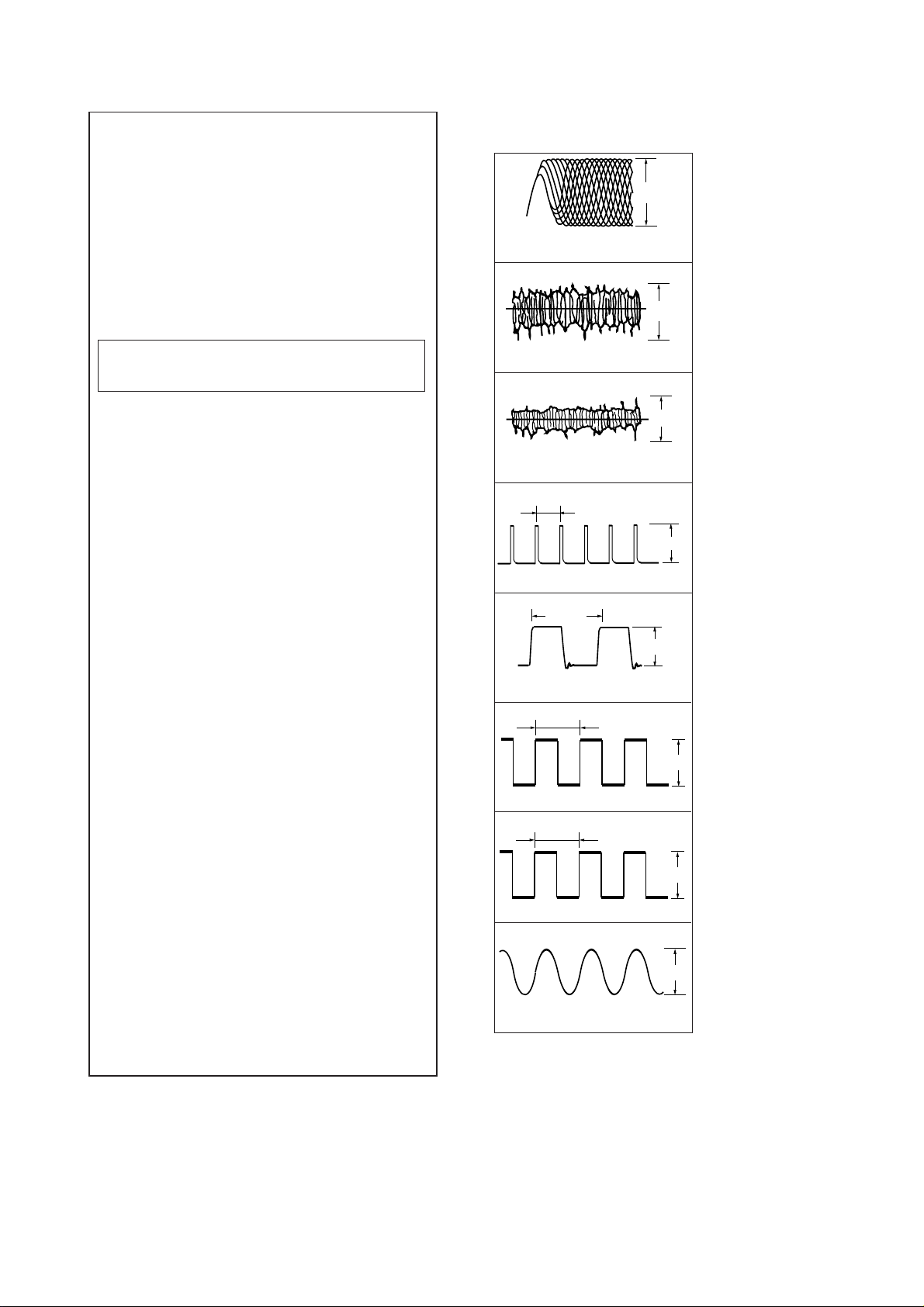
WAVEFORMS
– CD SECTION –
1
500mV/DIV, 500nsec/DIV
IC101 #£ RFO
2
200mV/DIV, 1µsec/DIV
IC101 2 FEI
3
IC101 $¶ TEI
4
7.8µsec
IC103 @¶ MDP
5
230µsec
IC103 ^º XPCK
6
IC103 ^™ RFCK
7
IC103 &¢ WFCK
8
16.9344MHz
IC103 *ª XTAI
1.3Vp-p
0.5Vp-p
2.5Vp-p
5Vp-p
2.6Vp-p
– 35 –
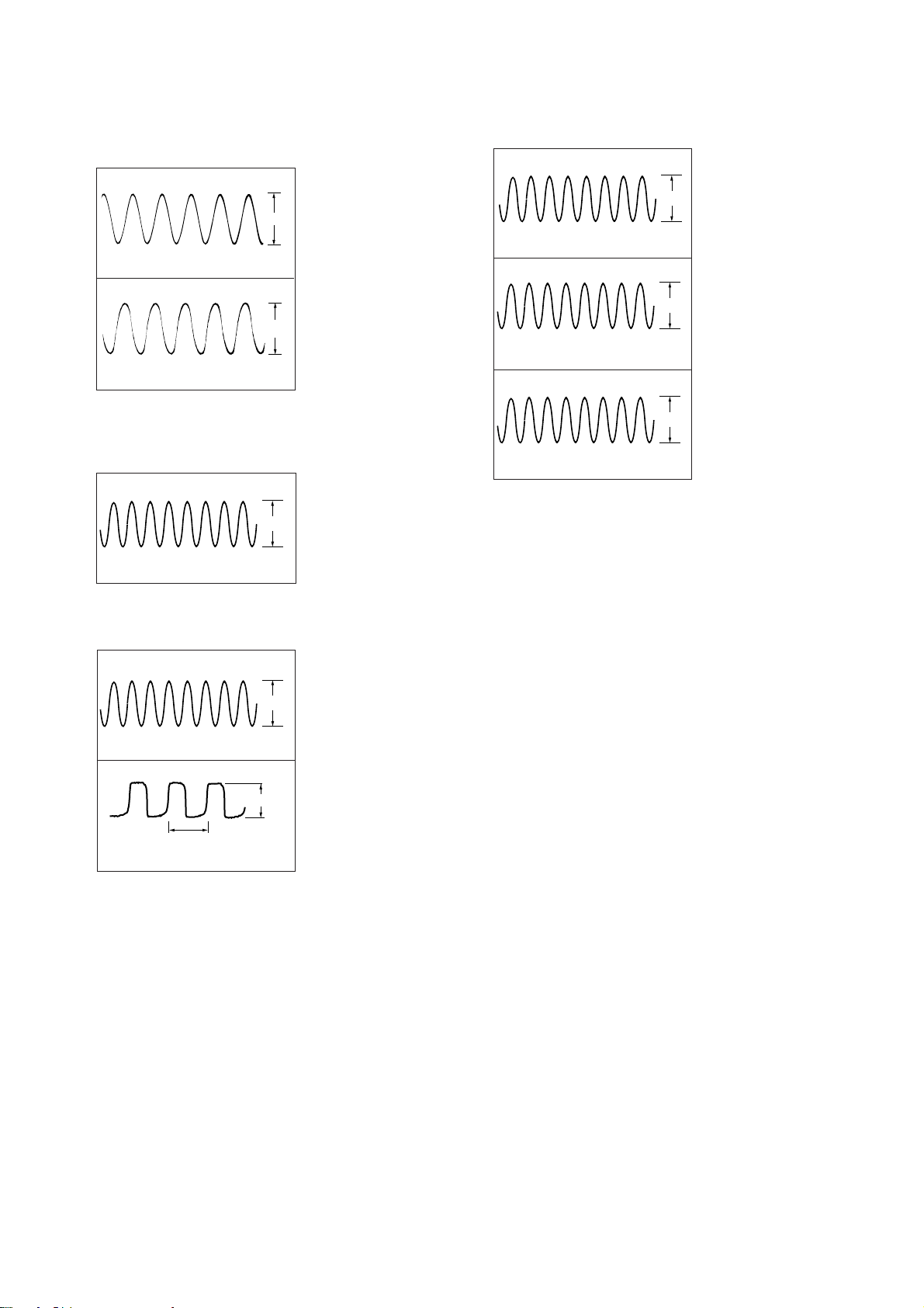
– TUNER SECTION –
(AEP, UK, German model)
1
4.2Vp-p
4.5MHz
IC21 @¢ XOUT
2
2Vp-p
4.332MHz
IC1752 !¢ OEC O
– TUNER SECTION –
(East European, CIS model)
1
4.2Vp-p
4.5MHz
IC21 @¢ XOUT
– DISPLAY SECTION –
1
4Vp-p
8MHz
IC601 8 X-OUT
2
4.3Vp-p
8MHz
IC801 2 X-OUT
3
3.6Vp-p
4.09MHz
IC851 2 TX
– MAIN SECTION –
1
5MHz
IC501 0 X2
2
32.768kHz
IC501 !£ XT2
5.5Vp-p
5Vp-p
– 36 –
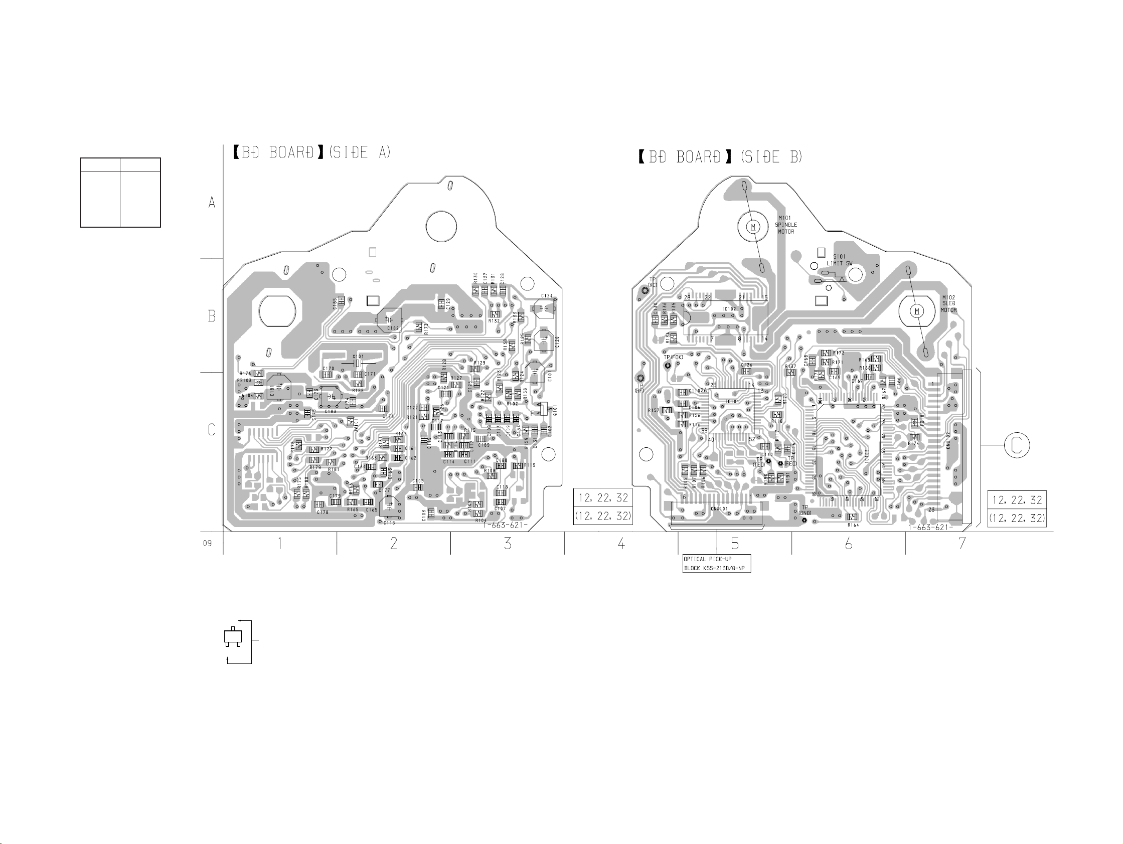
HCD-GRX8/R800/RX88/RX99
d
• Semiconductor
Location
Ref. No. Location
IC101 C-5
IC102 B-5 IC103 C-6
Q101 C-3
7-3. PRINTED WIRING BOARD — CD SECTION —
• See page 20 for Circuit Boards Location.
• Indication of transistor
C
Q
These are omitte
EB
(Page 38)
– 37 – – 38 –
 Loading...