

Page 1
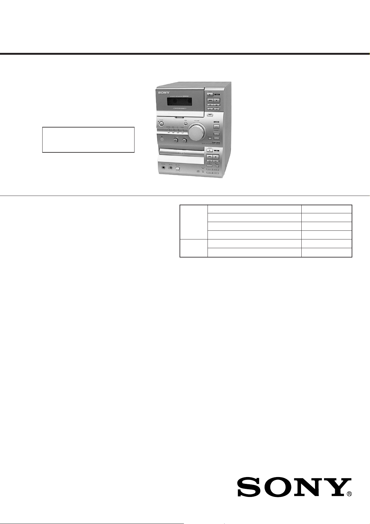
HCD-VP11
SERVICE MANUAL
Note
CD block, tape dec k block and
tuner pack are supplied with
the assembled block.
HCD-VP11 is the Amplifier, CD
player , Tape Deck and Tuner section
in CMT-VP11.
Dolby noise reduction manufactured under license
from Dolby Laboratories Licensing Corporation.
“DOLBY” and the double-D symbol a are trademarks of Dolby Laboratories Licensing Corporation.
CD
Section
Tape deck
Section
E Model
Model Name Using Similar Mechanism NEW
CD Mechanism Type CDM55-K5BD42
Base Unit Name BU-K5BD42
Optical Pick-up Name KSM-213CKP
Model Name Using Similar Mechanism HCD-CP11
Tape Transport Mechanism Type TCB-020
SPECIFICATIONS
Amplifier section
The following measured at 230 V AC, 60 Hz
DIN power output (rated): 30 + 30 W
Continuous RMS power output (reference):
The following measured at 220 V AC, 60 Hz
DIN power output (rated): 24 + 24 W
Continuous RMS power output (reference):
Inputs
MD IN (phono jacks): Sensitivity 500 mV, impedance
VIDEO IN (phono jacks): Sensitivity 250 mV, impedance
MIC (mini jack): sensitivity 1 mV,
Outputs
LINE OUT (phono jacks): Sensitivity 250 mV, impedance
OPTICAL DIGITAL OUT (CD):
VIDEO OUT (phono jack):
PHONES (stereo phone jack):
(6 Ω at 1 kHz, DIN)
35 + 35 W
(6 Ω at 1 kHz, 10% THD)
(6 Ω at 1 kHz, DIN)
27 + 27 W
(6 Ω at 1 kHz, 10% THD)
47 k
Ω
Ω
47 k
impedance 10 k
Ω
1 k
Optical
max. output level 1 Vp-p,
unbalanced, Sync negative, load
impedance 75
Accepts headphones with an
impedance of 8
Ω
Ω
Ω
or more
VIDEO CD/CD player section
System Compact disc and digital audio and
Laser Semiconductor laser
Laser output MAX 44.6
Wavelength 780 - 790 nm
Video color system format
OPTICAL DIGITAL OUT (CD)
(Square optical connector jack, rear panel)
Wavelength 660 nm
Output Level –18 dBm
video system
(λ=780 nm)
Emission duration: continuous
µ
W*
* This output is the value
measured at a distance of
200 mm from the objective
lens surface on the optical
pick-up block with 7 mm
aperture.
NTSC, PAL
— Continued on next page —
MICRO Hi-Fi COMPONENT SYSTEM
Page 2

Tape player section
Recording system 4-track 2-channel stereo
Frequency response (DOLBY NR OFF)
50 - 13,000 Hz (±3 dB), using a
Sony TYPE I cassette
50 - 14,000 Hz (±3 dB),
using a Sony TYPE II cassette
Tuner section
FM stereo, FM/AM superheterodyne tuner
FM tuner section
Tuning range 87.5 - 108.0 MHz
Antenna FM wire antenna
Antenna terminals 75 Ω unbalanced
Intermediate frequency 10.7 MHz
AM tuner section
Tuning range
Middle Eastern model: 531 - 1,602 kHz
Other models: 530 - 1,710 kHz
Antenna AM loop antenna, external antenna
Intermediate frequency 450 kHz
(50-kHz step)
(with the tuning interval set at
9 kHz)
(with the tuning interval set at
10 kHz)
531 - 1,602 kHz
(with the tuning interval set at
9 kHz)
terminal
General
Power requirements 220 - 240 V AC , 50/60 Hz
Power consumption 75 W
Dimensions (w/h/d) Approx. 190 × 252 × 310 mm
Mass Approx. 5.7 kg
Supplied accessories Remote commander (1)
Adjustable with voltage selector
incl. projecting parts and controls
AM loop antenna (1)
FM wire antenna (1)
Batteries (2)
Video connecting cord (1)
Design and specifications are subject to change
without notice.
SAFETY CHECK-OUT
After correcting the original service problem, perform the following
safety checks before releasing the set to the customer.
1. Check the area of your repair for unsoldered or poorly-soldered
connections. Check the entire board surface for solder splashes
and bridges.
2. Check the interboard wiring to ensure that no wires are
"pinched" or contact high-wattage resistors.
3. Look for unauthorized replacement parts, particularly
transistors, that were installed during a previous repair . Point
them out to the customer and recommend their replacement.
4. Look for parts which, through functioning, show obvious signs
of deterioration. Point them out to the customer and
recommend their replacement.
5. Check the B+ voltage to see it is at the values specified.
6. Flexible Circuit Board Repairing
• Keep the temperature of the soldering iron around 270˚C
during repairing.
• Do not touch the soldering iron on the same conductor of the
circuit board (within 3 times).
• Be careful not to apply force on the conductor when soldering
or unsoldering.
2
Page 3
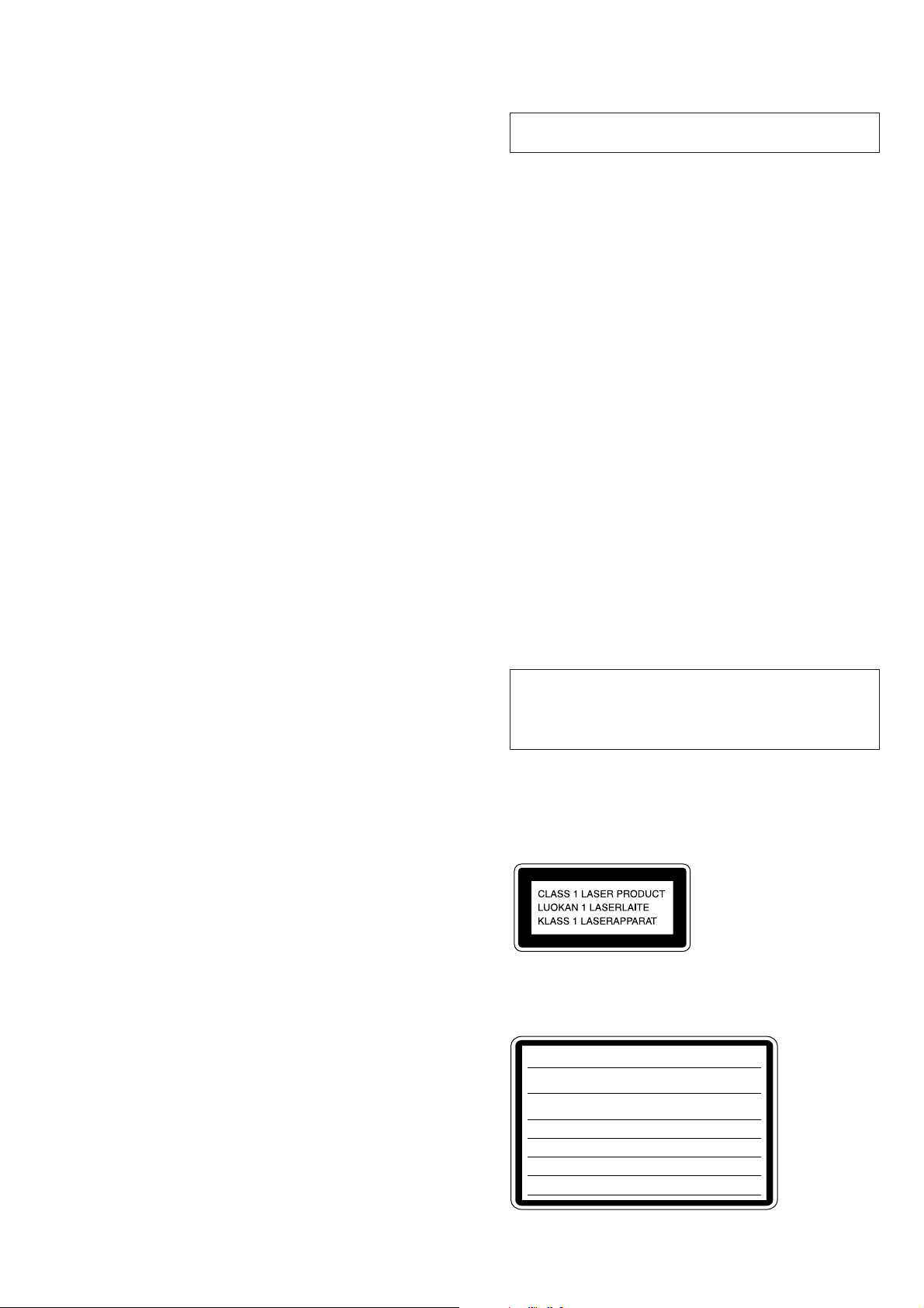
TABLE OF CONTENTS
SECTION 1
SERVICING NOTES
1. SERVICING NOTES······················································3
2. GENERAL·········································································· 4
3. DISASSEMBLY ································································ 6
4. SERVICE MODE··························································· 10
5. ELECTRICAL ADJUSTMENTS······························· 11
6. DIAGRAMS
6-1. Circuit Boards Locations ··················································· 13
6-2. Block Diagram – MAIN Section – ···································· 14
6-3. Block Diagram
– DISPLAY/POWER SUPPLY Section – ························· 15
6-4. Printed Wiring Board – MAIN Section – ·························· 16
6-5. Schematic Diagram – MAIN Section (1/2) – ···················· 17
6-6. Schematic Diagram – MAIN Section (2/2) – ···················· 18
6-7. Printed Wiring Boards
– LCD/HEADPHONE/LOADING/SPEAKER Section –
····· 19
6-8. Schematic Diagrams
– HEADPHONE/SPEAKER Section – ····························· 19
6-9. Printed Wiring Boards – CONTROL Section –·················20
6-10.Schematic Diagram – CONTROL Section –····················· 21
6-11.Printed Wiring Board – POWER Section – ······················· 22
6-12.Schematic Diagram – POWER Section –··························23
6-13.IC Block Diagrams ···························································· 24
6-14.IC Pin Function Description ·············································· 25
7. EXPLODED VIEWS····················································· 27
NOTES ON HANDLING THE OPTICAL PICK-UP
BLOCK OR BASE UNIT
The laser diode in the optical pick-up block may suffer electrostatic
break-down because of the potential difference generated by the
charged electrostatic load, etc. on clothing and the human body.
During repair, pay attention to electrostatic break-down and also
use the procedure in the printed matter which is included in the
repair parts.
The flexible board is easily damaged and should be handled with
care.
NOTES ON LASER DIODE EMISSION CHECK
The laser beam on this model is concentrated so as to be focused on
the disc reflective surface by the objective lens in the optical pickup block. Therefore, when checking the laser diode emission,
observe from more than 30 cm away from the objective lens.
Notes on chip component replacement
• Never reuse a disconnected chip component.
• Notice that the minus side of a tantalum capacitor may be damaged by heat.
Flexible Circuit Board Repairing
• Keep the temperature of the soldering iron around 270 ˚C during repairing.
• Do not touch the soldering iron on the same conductor of the
circuit board (within 3 times).
• Be careful not to apply force on the conductor when soldering
or unsoldering.
8. ELECTRICAL PARTS LIST·····································32
SAFETY-RELATED COMPONENT WARNING!!
COMPONENTS IDENTIFIED BY MARK 0 OR DOTTED LINE WITH
MARK 0 ON THE SCHEMATIC DIAGRAMS AND IN THE PARTS
LIST ARE CRITICAL TO SAFE OPERATION. REPLACE THESE
COMPONENTS WITH SONY PARTS WHOSE PART NUMBERS
APPEAR AS SHOWN IN THIS MANUAL OR IN SUPPLEMENTS
PUBLISHED BY SONY .
CAUTION
Use of controls or adjustments or performance of procedures
other than those specified herein may result in hazardous
radiation exposure.
This appliance is classified as a CLASS 1 LASER product.
The CLASS 1 LASER PRODUCT MARKING is located on
the rear exterior.
Laser component in this product is capable of emitting radiation
exceeding the limit for Class 1.
The following caution label is located inside the unit.
CAUTION :
INTERLOCKS DEFEATED. AVOID EXPOSURE TO BEAM.
ADVARSEL :
SIKKERHEDSAFBRYDERE ER UDE AF FUNKTION. UNDGÅ UDSAETTELSE
FOR STRÅLING.
VORSICHT :
ABDECKUNG GEÖFFNET UND SICHERUEITSVERRIEGELUNG
ÜBERBRÜCKT. NICHT DEM STRAHL AUSSETZEN.
VARO!:
TIINA NÄKYMÄTTÖMÄLLE LASERSÄTEILYLLE. ÄLÄ KATSO SÄTEESEEN.
VARNING :
OCH SPÄRREN ÄR URKOPPLAD. BETRAKTA EJ STRÅLEN.
ADVERSEL :
SIKKERHEDSLÅS BRYTES. UNNGÅ EKSPONERING FOR STRÅLEN.
VIGYAZAT!:
GÁRVESZÉLY
INVISIBLE LASER RADIATION WHEN OPEN AND
USYNLIG LASERSTRÅLING VED ÅBNING NÅR
UNSICHTBARE LASERSTRAHLUNG, WENN
AVATTAESSA JA SUOJALUKITUS OHITETTAESSA OLET ALT-
OSYNLING LASERSTRÅLING NÄR DENNA DEL ÄR ÖPPNAD
USYNLIG LASERSTRÅLING NÅR DEKSEL ÅPNES OG
A BURKOLAT NYITÁSAKOR LÁTHATATLAN LÉZERSU-
!
KERÜLJE A BESUGÁRZÁST!
3
Page 4
SECTION 2
GENERAL
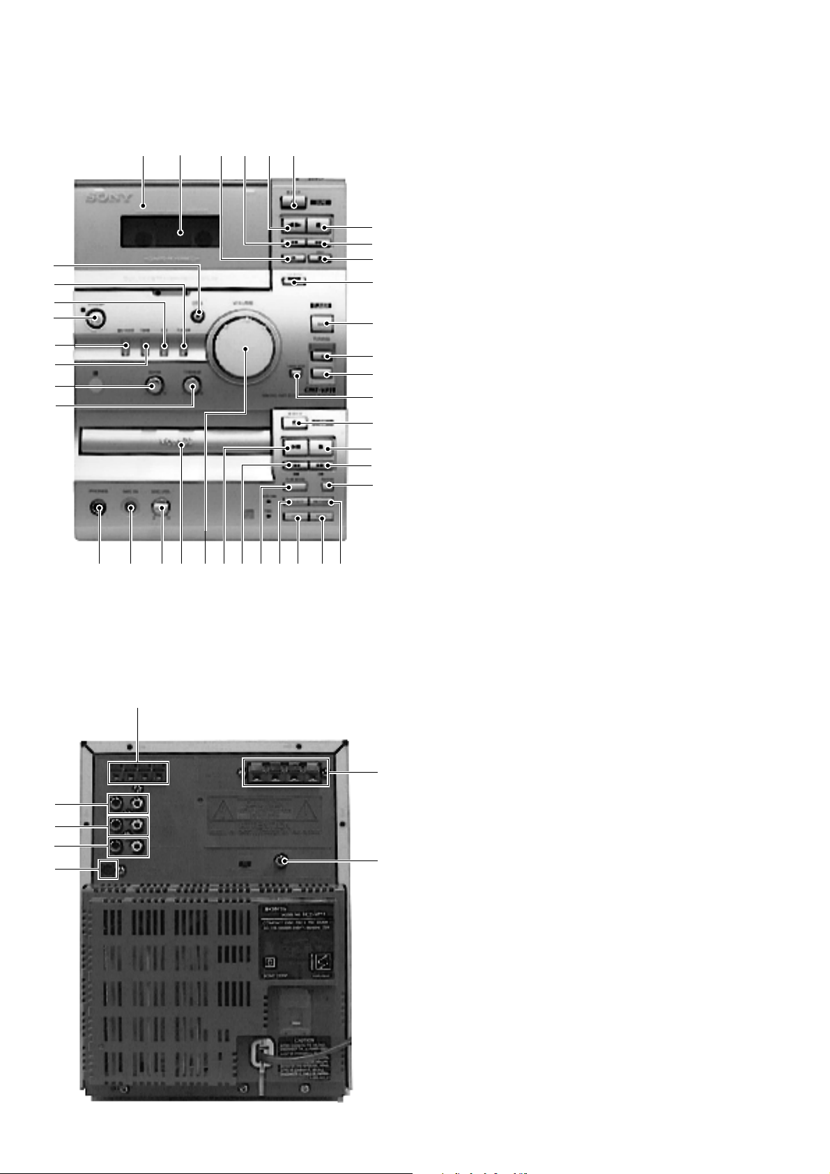
LOCATION OF CONTROLS
• Front View
2
1
ql
w;
wa
ws
wd
wf
wg
wh
wk wl eh ej
• Rear View
1
ea
1 TAPE deck
2 Liquid crystal display
3 TAPE X button
6543
7
8
9
0
qa
qs
qd
qf
qg
qh
qj
qk
ef eg
edese;wj
ek
4 TAPE m button
5 TAPE Y button
6 TAPE Z button
7 TAPE x button
8 TAPE M button
9 TAPE REC z button
0 CD SYNC button and indicator
qa BAND button
qs TUNING + button
qd TUNING – button
qf TUNING MODE button
qg CD EJECT Z button
qh CD x button
qj CD > button
qk CD REPEAT button
ql DSG button and indicator
w; TUNER button and indicator
wa CD button and indicator
ws STANDBY ?/1 button and indicator
wd MD/VIDEO button and indicator
wf TAPE button and indicator
wg BASS knob
wh TREBLE knob
wj PHONES jack
wk MIC IN jack
wl MIC VOL knob
e; CD disc tray
ea VOLUME knob
es CD u button
ed CD . button
ef CD PLAY MODE button
eg SELECT button
eh PREV button
ej RETURN button
ek NEXT button
4
5
6
7
4
2
3
1 ANTENNA terminals
2 SPEAKER terminals
3 VIDEO OUT jack
4 LINE OUT jacks
5 MD IN jacks
6 VIDEO IN jacks
7 CD DIGITAL OUT OPTICAL connector
Page 5
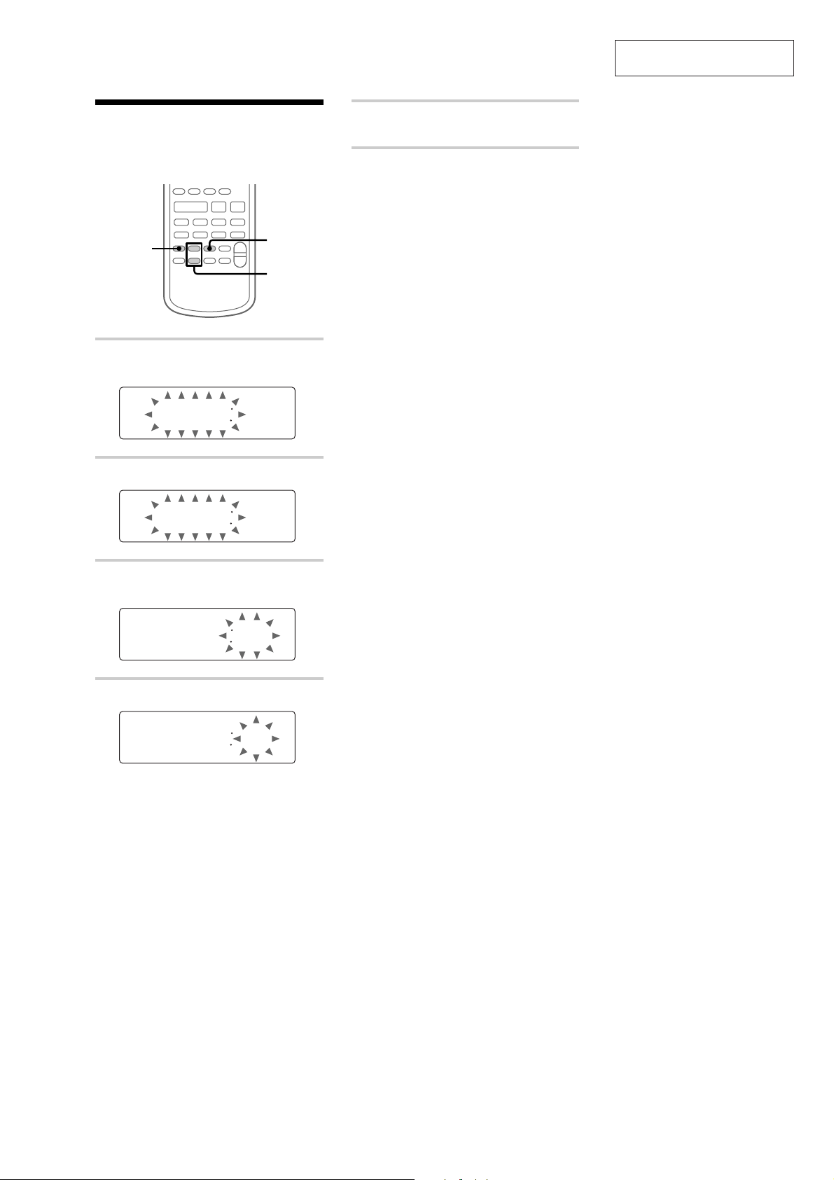
Step 2: Setting the time
Before you can use the system’s timer functions,
set the internal clock.
Xx
N
nN
.> z
1
mM y
#
2
3,5
+
–
2,4
1
Press TIMER SET.
The hour indication flashes.
AM1200
5
Press ENTER.
The clock will begin operating.
To reset the system clock
You can reset the system clock even when the
system is on or off. To reset the time while the
system is on, do the following:
1 Press TIMER SET.
2 Press +/– repeatedly until “SET CLOCK”
appears, then press ENTER.
3 Repeat steps 2 to 5 in “Step 2: Setting the
time”.
Tip
If you make a mistake, start over from step 1.
This section is extracted from
instruction manual.
2
Press +/– repeatedly to set the hour.
AM1100
3
Press ENTER.
The minute indication flashes.
AM1100
4
Press +/– repeatedly to set the minute.
AM1110
5
Page 6
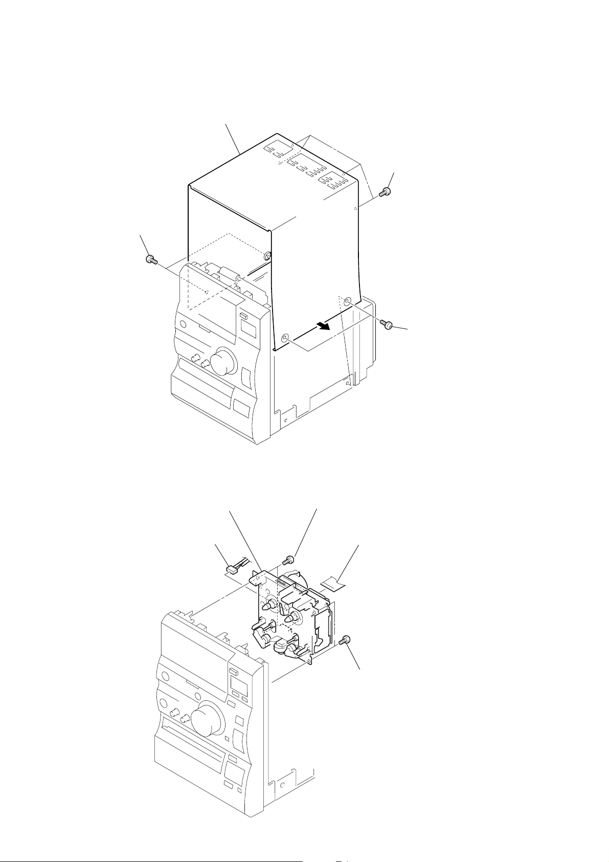
SECTION 3
)
s
DISASSEMBLY
Note: Follow the disassembly procedure in the numerical order given.
3-1. COVER (UPPER)
4
Cover (upper)
1
Two screws
(case3 TP2)
2
Four screws
(BTP3
3
×
8)
Two screws
(case3 TP2
3-2. TAPE MECHANISM DECK
5
Tape
mechanism deck
2
Connector
3
Two screws
×
8)
(BTP3
1
Flat wire (12 core)
4
Two screw
(BTP3 × 8)
6
Page 7
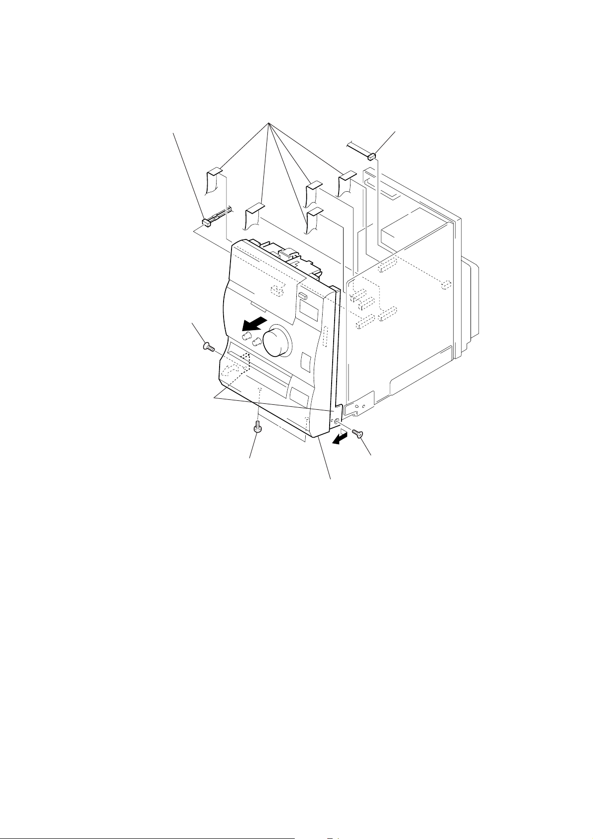
3-3. FRONT PANEL SECTION
3
Connector
4
Screw
(TP3
×
6)
2
Flat wire
1
Connector
(CN303)
Two claws
5
Two screws
(BTP3
×
8)
7
(There is a claw.)
6
Screw
(KTP3
Front panel section
×
6)
7
Page 8
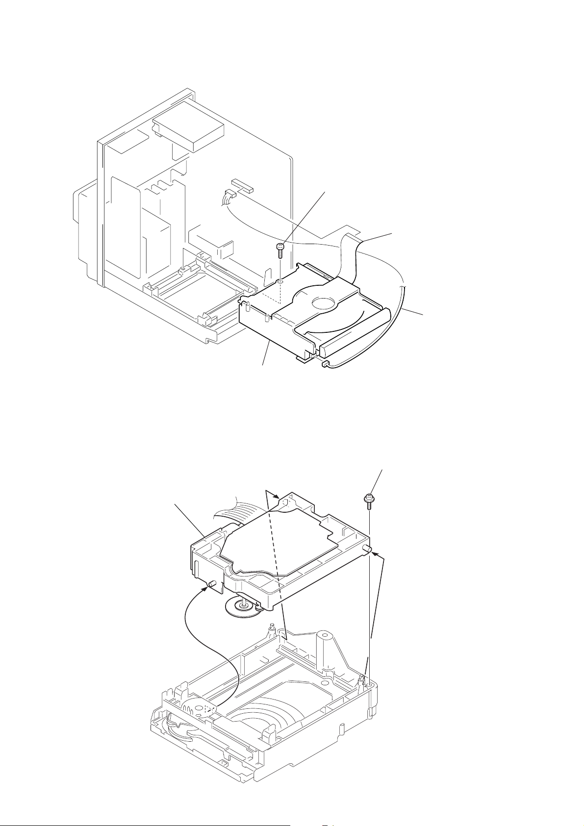
3-4. CD MECHANISM DECK
r
w
3
Screw
(BTP3 × 8)
2
flat wire (19 core)
(CN805)
1
connecto
3-5. UPPER CHASSIS
2
Upper chassis
4
CD mechanism deck
1
Scre
8
Page 9
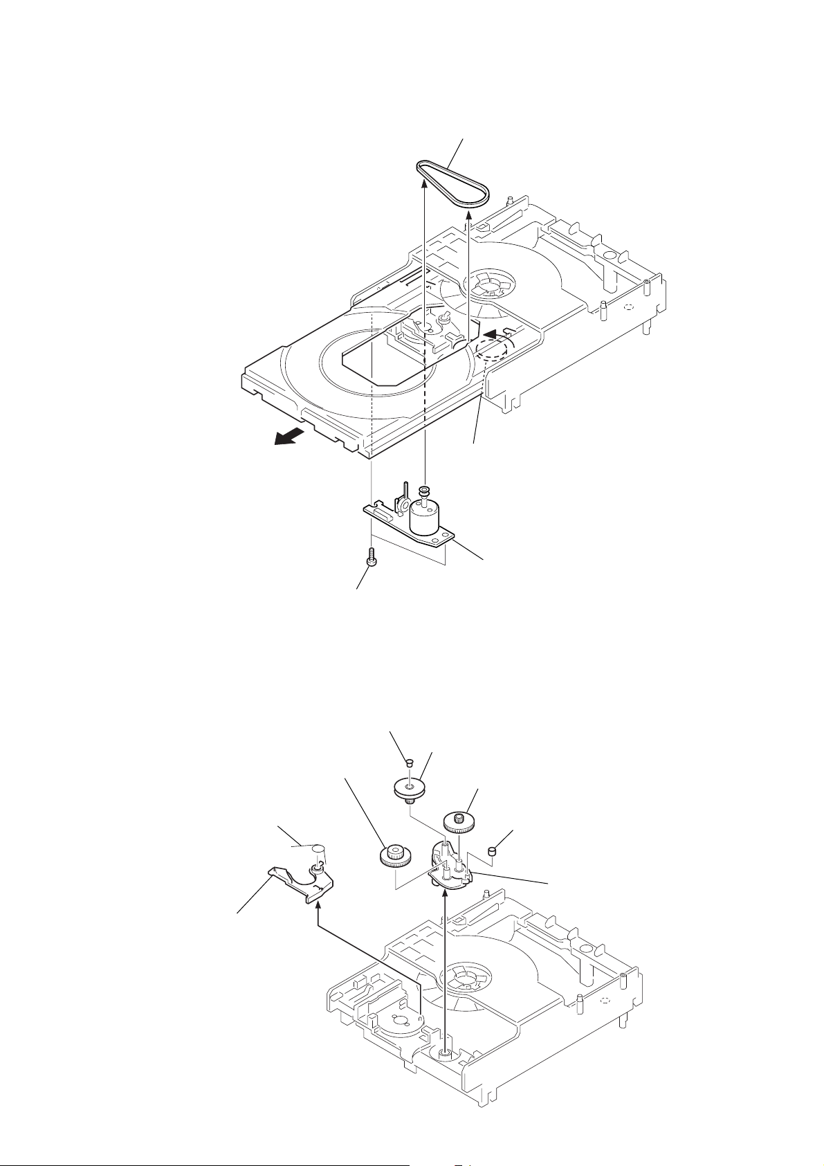
3-6. TRA Y
5
Pull the tray
2
Belt
A
1
Rotate the control cam in
the direction of arrow
A
3-7. CAM
2
SW lever
1
Torsion spring
3
6
Two screws
3
Gear
Spacer (55)
4
Pulley
5
4
Gear
Motor board
7
Roller
8
Cam
9
Page 10
SECTION 4
SERVICE MODE
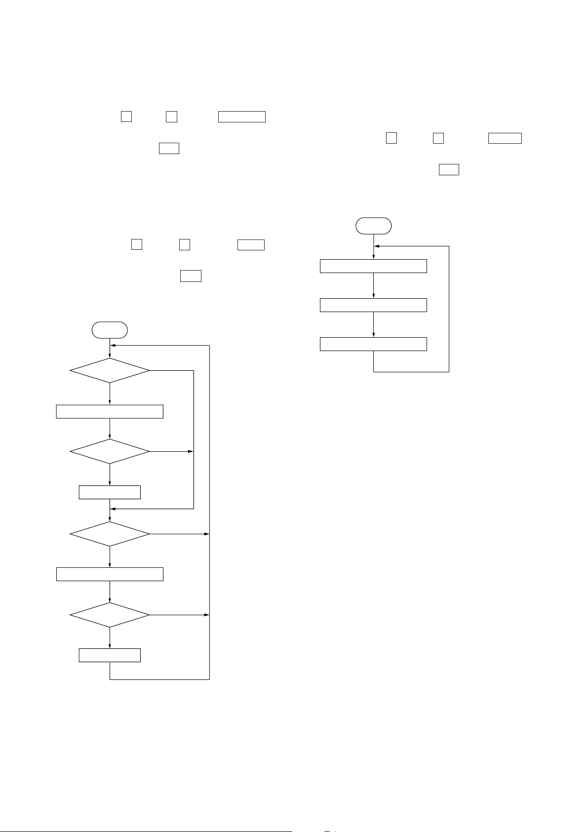
[Liquid Crystal Display All Lit Check Mode]
Procedure:
1. Set to standby state.
2. Press three buttons of x (TAPE), x (CD), and MD/VIDEO
simultaneously.
3. Liquid crystal display are all turned on.
4. T o exit from this mode, press the ?/1 button to turn the power
OFF .
[Tape Deck Aging Mode]
This mode can be used for operation check of tape deck section.
Procedure:
1. Set a tape in the tape deck.
2. Set to standby state.
3. Press three buttons of x (TAPE), x (CD), and TAPE
simultaneously.
4. The aging is executed in bellow sequence.
5. T o exit from the aging mode, press the ?/1 button to turn the
power OFF.
Aging mode sequence:
Start
[CD Aging Mode]
This mode can be used for operation check of CD section.
Procedure:
1. Load a CD disc.
2. Set to standby state.
3. Press three buttons of x (TAPE), x (CD), and TUNER
simultaneously.
4. The aging is executed in bellow sequence.
5. T o exit from the aging mode, press the ?/1 button to turn the
power OFF.
Aging mode sequence:
Start
Open the disc tray
Close the disc tray
Play the last track
FWD Play
1 minute
REC pause for 3 seconds
FWD REC
3 minutes
Fast forward
REV Play
1 minute
REC pause for 3 seconds
REV REC
3 minutes
Shut off
Shut off
Shut off
Shut off
10
Rewind
Page 11
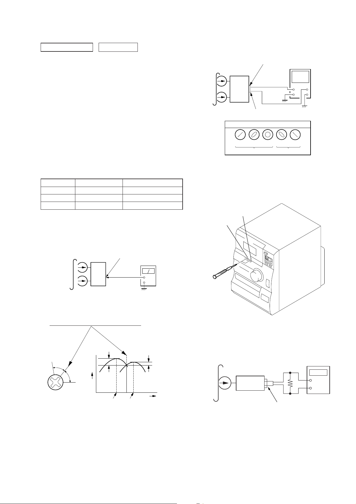
SECTION 5
r
e
ELECTRICAL ADJUSTMENTS
DECK SECTION
Note: Confirm each contents of this section first of all. If the results are
not satisfied, do the adjustment.
0 dB=0.775 V
1. Demagnetize the record/playback head with a head
demagnetizer.
2. Do not use a magnetized screwdriver for the adjustments.
3. After the adjustments, apply suitable locking compound to the
parts adjust.
4. The adjustments should be performed with the rated power
supply voltage unless otherwise noted.
5. The adjustments should be performed in the order given in this
service manual. (As a general rule, playback circuit adjustment
should be completed before performing recording circuit
adjustment.)
6. The adjustments should be performed for both L-CH and RCH.
7. Switches and controls should be set as follows unless otherwise
specified.
• Test T ape
Tape Signal Used for
P-4-A100 10 kHz, –10 dB Azimuth Adjustment
WS-48B 3 kHz, 0 dB Tape Speed Check
P-4-L300 315 Hz, 0 dB Level Adjustment
Record/Playback Head Azimuth Adjustment
Procedure:
1. Mode: Playback
3. Mode: Playback
MAIN board
test tape
P-4-A100
(10 kHz, –10 dB)
L-CH
MAIN
board
CN301
set
R-CH
in phase 45°90°135°180
LINE OUT jack (PJ301)
L-CH
R-CH
waveform of oscilloscope
good
oscilloscop
wrong
H
V
°
4. Repeat step 1 to 3 in playback (REV) mode.
5. After the adjustments, apply suitable locking compound to the
pats adjusted.
Adjustment Location:
reverse
forward
test tape
P-4-A100
(10 kHz, –10 dB)
MAIN board
LINE OUT jack (PJ301)
L-CH, R-CH
set
level mete
+
–
2. Turn the adjustment screw and c heck output peaks. If the peaks
do not match for L-CH and R-CH, turn the adjustment screw
so that outputs match within 1dB of peak.
Output
level
within
1dB
L-CH
peak
R-CH
peak
within
1dB
Screw
position
L-CH
peak
Screw
position
R-CH
peak
Tape Speed Adjustment
Procedure :
Mode : Playback
test tape
WS-48B
(3kHz, 0dB)
set
LINE OUT
digital frequency
counter
32
Ω
+
–
Adjust the tape speed adjustment control inside motor, so that the
frequency counter reading becomes 3,000 ±90 Hz.
Sample Value of Wow and flutter
W.RMS (JIS) less than 0.3%
(test tape : WS-48B)
11
Page 12
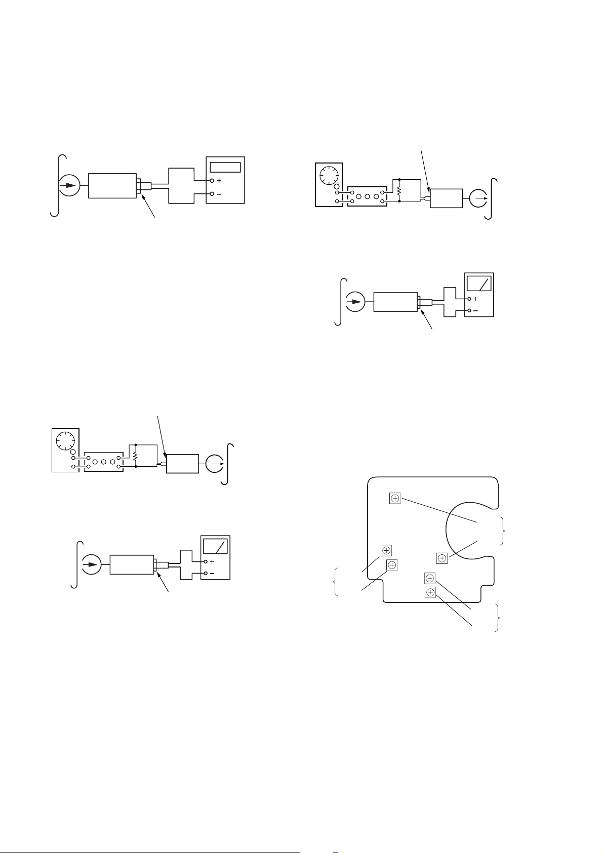
Playback Level Adjustment
r
e
r
e
r
Record Level Adjustment
Procedure:
Mode: FWD playback
test tape
P-4-L300
(3kHz, 0dB)
frequency counte
set
LINE OUT
Adjust R V101 (L-CH) and R V201 (R-CH), so that adjustment within
the following adjustment level.
Adjustment level:
LINE OUT level: –7.7 ± 0.5 dB (301.5 to 338.5 mV)
Level difference between the channels: within ± 0.5 dB
Confirm that the LINE OUT level does not change even though
play and stop are repeated.
Record Bias Adjustment
Procedure:
1. Record mode.
LINE IN
1) 315 Hz
2) 10 kHz
AF OSC
attenuator
600
Ω
} 50 mV (–23.8 dB)
blank tap
CS-123
set
Procedure:
1. Record mode.
LINE IN
315Hz 50 mV (–23.8 dB)
AF OSC
attenuator
600
Ω
set
blank tap
CS-123
2. Playback mode.
recorded
position
set
LINE OUT
level mete
3. Confirm playback the signal recorded in step 1 become
adjustment level as follows.
4. If these levels do not adjustment level, adjust the RV103 (LCH) and RV203 (R-CH), on the MAIN board to repeat steps 1
to 3.
Adjustment level:
LINE OUT level: –23.8 dB ± 0.5 dB (47.2 to 53.0 mV)
Adjustment Location: TC board
2. Playback mode.
recorded
position
set
LINE OUT
level mete
3. Confirm playback the signal recorded in step 1 become
adjustment level as follows.
4. If these levels do not adjustment level, adjust the RV102 (LCH) and RV202 (R-CH), to repeat steps 1 to 3.
Adjustment level:
The playback outpout of 10 kHz level difference adjust
315 Hz reference should be 0 dB ± 0.5 dB.
Play back
level
RV201
RV101
RV203
RV103
RV102
RV202
Record
level
Record
bias
12
Page 13

SECTION 6
d
V
DIAGRAMS
CD SECTION
Note:
1. CD Block is basically constructed to operate without
adjustment.
2. Use YEDS-18 disc (3-702-101-01) unless otherwise indicated.
3. Use an oscilloscope with more than 10 MΩ impedance.
4. Clean the object lens by an applicator with neutral detergent
when the signal level is low than specified value with the
following checks.
5. Check the focus bias check when optical block is replaced.
Focus Bias Check
oscilloscope
(DC range)
BD board
TP (RF)
TP (VC)
Procedure :
1. Connect oscilloscope to TP (RF) and TP (VC) on the CD board.
2. Press the I/1 button to turn the power on, and press the Z
(CD) button to open the CD disc tray.
3. Put disc (YEDS-18) in and press the u (CD) button to playback.
4. Confirm that oscilloscope waveform is as shown in the figure
below. (eye pattern)
A good eye pattern means that the diamond shape ( ) in the
center of the waveform can be clearly distinguished.
+
–
s
VOLT/DIV: 200 m
TIME/DIV: 500 ns
– CD BOARD (Conductor Side) –
IC103
TP (RF)
TP (VC)
NOTE FOR PRINTED WIRING BOARDS AND SCHEMATIC DIAGARAMS
Note on Printed Wiring Board:
• X : parts extracted from the component side.
• Y : parts extracted from the conductor side.
• b : Pattern from the side which enables seeing.
• Wavef orms
– MAIN Board –
1
IC801 el (EXTAL1)
4.6Vp-p
5.0Vp-p
2
IC801 os (TX)
238ns
30.5µs
Note on Schematic Diagram:
• All capacitors are in µF unless otherwise noted. pF: µµF
50 WV or less are not indicated except for electrolytics
and tantalums.
• All resistors are in Ω and 1/
specified.
¢
•
• C : panel designation.
Note: The components identified by mark 0 or dotted line
• U : B+ Line.
• V : B– Line.
• H : adjustment for repair.
• Voltages are taken with a V OM (Input impedance 10 MΩ).
• Waveforms are taken with a oscilloscope.
• Circled numbers refer to waveforms.
• Signal path.
• Abbreviation
: internal component.
with mark 0 are critical for safety.
Replace only with part number specified.
Voltage variations may be noted due to normal production tolerances.
Voltage variations may be noted due to normal production tolerances.
F : TUNER
E : TAPE PLAY
a : TAPE RECORD
J : CD PLAY (ANALOG OUT)
c : CD PLAY (DIGITAL OUT)
SP : Singapore model.
MY : Malaysia model.
HK : Hong Kong model.
TH : Thai model.
EA : Saudi Arabia model.
4
W or less unless otherwise
Checking Location:
level:
1.2
±
0.1 Vp-p
6-1. CIRCUIT BOARDS LOCATION
LCD board
SPEAKER board
POWER board
VIDEO OUT board
HEADPHONE board
LOADING board
CONTROL board
MAIN boar
1313
Page 14

HCD-VP11
6-2. BLOCK DIAGRAM – MAIN Section –
J402
MIC
VIDEO IN
FM
75Ω
AM
MD IN
A
B
PJ301 (1/2)
L
R
L
R
ANTENNA
TU ON
REC/PB
R-CH
R-CH
MIC AMP
IC315(1/2)
RV200
ECHO
MUTING
Q102, 103
R-CH
TAPE DECK
L OUT
R OUT
L IN
R IN
BIAS ON/OFF
REC MUTE
DOLBY ON/OFF
REC/PB
LINE MUTE
SENSOR OUT
PLAY SW
PACK/REC-L/R TC-SW
+12V
SOL 12V
TUNER PACK
FM ANT
ANT GND
ANT GND
AM ANT
L-CH
R-CH
DI
DO
CK
CE
TUNED
MIC AMP
IC315(2/2)
LIN1
11
LIN2
12
LIN3
+
MUTING
Q106
R-CH
R-CH
R-CH
1
2
9
7
8
10
4
R-CH
13
LIN4
14
CAPSTAN/REEL
MOTOR DRIVE
Q657,659
TRIGGER
PLUNGER DRIVE
Q656,658
MOL
INPUT SELECT SWITCH
R-CH
LINE AMP
IC307
VOLUME
INL
15
INPUT SELECT SWITCH,
TONE CONTROL,
SDA
28
86
87
88
95
96
32
10
18
19
ELECTRICAL VOLUME
SCK
REC-BIAS
REC-MUTE
DOLBY
REC/PB
L-MUTE
TAPE-END
1
6
T-MODE
MOT-CON
4
SOL-CON
5
TU-DATA/SDA
TU-COUNT
TU-CLK
8
TU-CE
TUNED
2
SCL
1
30
CONTROL
16
CIRCUIT
IC301
SYSTEM CONTROLLER
IC801 (1/2)
TONE
CONTROL
CIRCUIT
AMP-MUTE
AU-MUTE
MD/VIDEO-ON
VCD-LED
22
97
24
23
LOUT
ATT
ROUT
MUTING
CONTROL SWITCH
Q303, 304
MUTING
CONTROL SWITCH
Q317, 318
LED DRIVE
Q853
LED DRIVE
Q500
6
R-CH
5
MUTING
Q101,107
R-CH
MUTING
Q111
R-CH
D313
D853
MD/VIDEO
D500
VCD
POWER AMP
IN+
3
10
R-CH
HEADPHONE
AMP
IC303
R-CH
IC101
MUTE
OUT
HP SW
Q393
MUTING
Q132
R-CH
14
R-CH
MUTE
R-CH
L
PJ301 (2/2)
LINE OUT
R
+
L
R
SJ301
SPEAKER
IMPEDANCE
USE 6Ω
–
+
–
C
J301
PHONES
CD DIGITAL OUT
OPTICAL
VIDEO OUT
SYSTEM
SELECT
S902
(DISC TRAY OPEN DET)
S901
(DISC TRAY CLOSE DET)
OPTICAL
TRANSCEIVER
IC308
B+
16
CD BLOCK
D-OUT
VIDEO-OUT
NTSC/AUTO/PAL
OPEN-SW
CLOSE-SW
CD-L-OUT
CD-R-OUT
S-ACK
S-CLK
S-SI
S-SO
S-REQ
S-RST MPEG-RST
R-CH
DISC TRAY OPEN/CLOSE
IN2OPEN
6 10
IN1CLOSE
5 2
MOTOR DRIVE
IC309
OUT2
OUT1
M
M901
DISC TRAY
OPEN/CLOSE
100
11
12
13
14
17
S-ACK
S-CLK
S-SI
S-SO
S-REQ
PBC-LED
TEX
15
92
TX
93
LED DRIVE
X802
32.768kHz
Q501
D501
PBC
• SIGNAL PATH
: TUNER
XTAL1
EXTAL1
40
X801
4.19MHz
39
: CD PLAY (ANALOG OUT)
: CD PLAY (DIGITAL OUT)
: TAPE PLAY
: TAPE RECORD
1414
Page 15

6-3. BLOCK DIAGRAM – DISPLAY/POWER SUPPLY Section –
HCD-VP11
LIQUID CRYSTAL
+5V
RESET SIGNAL
REMOTE CONTROL
RECEIVER
RV801
VOLUME
RV802
TREBLE
RV803
BASE
DISPLAY
LCD801
SWITCH
Q829,830
GENERATOR
IC803
IC802
ROTARY
ENCODER
RV801
ROTARY
ENCODER
RV802
ROTARY
ENCODER
RV803
S801 – 828
SYSTEM CONTROLLER,
LCD DRIVER
IC801 (2/2)
SYSTEM CONTROLLER (IC801) B+
54 – 85
SEG0 – SEG31
50 – 53
COM0 – COM3
99
WP
38
RESET
7
REG-CON
98
98
TC-ON
TC-ON
3
REMOCON
21
JOG-A
JOG-B
20
29
JOG-E
JOG-F
30
9
JOG-C
JOG-D
16
36 – 33
KEY1 – KEY4
16
RDS-ON
TU-ON
CD-ON
D.S.G.
CD-SYNC
31
25
94
26
27
CASSETTE HOLDER
(DISC TRAY ILLUMINATION)
LED DRIVE
LED DRIVE
Q854
Q854
LED DRIVE
Q855
LED DRIVE
Q852
LED DRIVE
Q856
LED DRIVE
Q857
BACK UP +5V
D657 – 660
(LCD BACK LIGHT)
BACK LIGHT
D851
STANDBY
I/u
D858
D801
D802
D814
D815
D854
TAPE
D855
TUNER
D852
CD
D856
DSG
D857
CD SYNC
B+ SWITCH
Q653, 654
B+ SWITCH
Q651, 652
LED DRIVE
Q858,859
LED B+
REGULATOR
CONTROL SWITCH
Q315, 316
REGULATOR
CONTROL SWITCH
Q321, 322
REGULATOR
CONTROL SWITCH
Q311, 312
D813
Q655
B+ SWITCH
Q661, 662
D812
FM CIRCUIT B+
TUNER PACK B+
TDA7439 (IC301) B+
AUDIO
CIRCUIT
FM 7.5V
+9V
+5V
CD BLOCK B+
+7.5V
+8V
CD BLOCK
+8V
–8V
+5.6V
REGULATOR
IC310
+8V
REGULATOR
IC311
+8V
REGULATOR
IC304
–8V
REGULATOR
IC305
+7.5V
REGULATOR
Q314
+9V
REGULATOR
Q313,D304
D307
+5V
REGULATOR
Q310
+7.5V REG
Q325,D306
+8V DET
Q326
+12V
REGULATOR
Q301-303
+12V
REGULATOR
Q350-351
POWER AMP
(IC101, 201)
VOLTAGE
SELECTOR
S901
POWER TRANSFORMER
T901
RECT
D911 – 914
B+
B–
RECT
D907 – 910
220-240V 110-120V
230V
115V
COM
REC/PB
TU ON
MUTE
F901
LINE
FILTER
LF901
AC IN
B
A
C
1515
Page 16

HCD-VP11
6-4. PRINTED WIRING BOARD – MAIN Section – • See page 13 for Circuit Boards Location.
• Semiconductor
Location
Ref. No. Location
D301 G-6
D303 B-5
D304 B-5
D305 G-5
D306 C-5
D307 B-5
D308 F-5
D311 E-5
D313 E-4
D350 G-5
D651 A-3
D652 B-3
D801 F-3
D802 E-3
D812 G-3
D813 G-3
D814 C-1
D815 A-3
IC101 F-7
IC201 E-7
IC301 C-6
IC303 D-7
IC304 F-5
IC305 G-5
IC307 B-6
IC308 C-7
IC309 F-5
IC310 E-5
IC311 F-5
IC312 B-4
IC315 D-7
IC801 F-2
IC803 F-3
A
B
C
12
(Page 19)
(Page 19)
(Page 20)
There are few cases that the part printed on this
diagram isn’t mounted in this model.
345678
Q101 B-7
Q102 C-7
Q103 C-7
Q106 A-6
Q111 C-7
Q201 B-7
Q202 C-7
Q203 C-7
Q206 A-6
Q211 C-7
Q301 G-6
Q302 G-6
Q303 G-6
Q307 E-4
Q308 E-4
Q310 G-5
Q311 G-5
Q312 G-5
Q313 A-5
Q314 B-5
Q315 B-5
Q316 B-5
Q317 F-4
Q318 F-4
Q321 A-5
Q322 A-5
Q350 G-5
Q351 G-5
Q352 G-5
Q393 D-7
Q651 G-4
Q652 F-4
Q653 G-4
Q654 G-4
Q655 G-4
Q656 B-3
Q657 B-3
Q658 B-4
Q659 B-4
D
(Page 19)
(Page 19)
E
(Page 22)
F
G
(Page 19)
16
1616
Page 17

6-5. SCHEMATIC DIAGRAM – MAIN Section (1/2) – • See page 24 for IC Block Diagram.
HCD-VP11
1717
Page 18

HCD-VP11
6-6. SCHEMATIC DIAGRAM – MAIN Section (2/2) – • See page 25 for IC Pin Function Description. • See page 13 for Waveforms.
PIN FUNCTION
1818
Page 19

• See page 13 for Circuit Boards Location.
• See page 18 for LCD BOARD Schematic Diagram.
• See page 17 for LOADING BOARD Schematic Diagram.
There are few cases that the part printed on this
diagram isn’t mounted in this model.
HCD-VP11
6-8. SCHEMATIC DIAGRAMS – HEADPHONE/SPEAKER Section –6-7. PRINTED WIRING BOARDS – LCD/HEADPHONE/LOADING/SPEAKER Section –
A
B
C
(Page 16)
12
(Page 16)
(Page 16)
345
D
E
F
G
(Page 16)
(Page 16)
1919
Page 20

HCD-VP11
6-9. PRINTED WIRING BOARDS – CONTROL Section – • See page 13 for Circuit Boards Location.
There are few cases that the part printed on this
diagram isn’t mounted in this model.
• Semiconductor
Location
Ref. No. Location
D500 G-3
D501 H-3
D851 C-7
D852 D-5
D853 D-6
D854 D-5
D855 D-4
D856 C-4
D857 B-2
D858 E-5
A
B
C
12
34567
D
E
F
(Page 16)
G
H
2020
Page 21

6-10. SCHEMATIC DIAGRAM – CONTROL Section –
HCD-VP11
+
–
2121
Page 22

HCD-VP11
6-11. PRINTED WIRING BOARD – POWER Section – • See page 13 for Circuit Boards Location.
• Semiconductor
Location
Ref. No. Location
D907 E-5
D908 E-5
D909 E-4
D910 E-4
D911 C-6
D912 D-6
D913 D-6
D914 D-7
A
12
B
There are few cases that the part printed on this
diagram isn’t mounted in this model.
345678
C
D
E
PIN FUNCTION
(Page 16)
2222
Page 23

6-12. SCHEMATIC DIAGRAM – POWER Section –
HCD-VP11
The components identified by mark 0 or dotted
line with mark 0 are critical for safety.
Replace only with part number specified.
23
Page 24

6-13. IC BLOCK DIAGRAMS
8
7
6
5
1
2
3
4
2CH
1CH
VCC
OUT2
–IN2
+IN2
OUT1
–IN1
+IN1
VEE
– MAIN Board –
IC101, 201 TDA7296
IC303 NJM3414AMP(TE2)
BIPOLAR
TRANSCONDACTANCE
INPUT STAGE
–
+
IN–
IN+
STBY-GND
IN+ MUTE
IC301 TDA7439
SCL
DIG GND
TREBLE (R)
TREBLE (L)
MIN (L)
NC
MOUT (L)
BOUT (L)
LEVEL SHIFTING
BIN (L)
BOUT (R)
MOS GAIN &
STAGE
BOOST-
STRAP
BOOSTSTRAP
BIN (R)
MOUT (R)
MIN (R)
+VS
STANDBY/
MUTE
–VS
STBY
INR
18
THERMAL
SHUTDOWN
MOS
OUTPUT
STAGE
MUTE
SHORT
CIRCUIT
PROTECTION
NC
NC
MUX OUT (R)
14 1512 1310 118 96 753 41 2
OUT
+PWVS
–PWVS
IC309 KA3082
INL
161727282930 22 21 20 1926 25 24 23
IIC BUS
DECODER &
LATCH
VREF
SUPPLY
1 2 3 4 5 6
CREF
VS
AGND
SDA
ROUT
LOUT
VOLUME
TREBLE
MIDDLE
BASS
SPEAKER
ATTENUATOR
GAIN AMP
MULTIPLEXER
7 8
9 10
R-IN4
R-IN3
R-IN2
11 12
R-IN1
VOLUME
TREBLE
MIDDLE
BASS
SPEAKER
ATTENUATOR
GAIN AMP
MULTIPLEXER
13 14
L-IN1
L-IN2
L-IN3
L-IN4
DRIVER OUT
PRE DRIVER
BIAS
GND
OUT1
15
VZ1
VCTL
LOGIC
SWITCH
5 6 7 8 9 101 2 3 4
IN1
IN2
VCC1
TSD
VCC2
VZ2
OUT2
MUX OUT (L)
24
Page 25

6-14. IC PIN FUNCTION DESCRIPTION
e
• MAIN BOARD IC801 CXP83120A-041Q (SYSTEM CONTROLLER, LCD DRIVER)
Pin No. Pin Name I/O Description
1 TAPE-END I
2
RDS-CLK
3 REMOCON I
4 MOT-CON O
5 SOL-CON O
6 T-MODE I
7 REG-CON O
8
9
CD-CLK
TUNED
CD-DATA/
10
TU-DATA/
SDA
11
12
13
14
15
16
17
18
19
CD-SQCK
CD-SQSO/
RDS-DATA
TRAY-OPEN
CD-MUTE
TRAY-CLOSE
CD-SENSE1
CD-XRST
CD-SENSE2/
TU-COUNT
CD-LATCH/
TU-CE
20 JOG-B I
21 JOG-A I
22
23
24
AMP-MUTE
AMP-STBY
VIDEO-ON
25 TU-ON O
26 D.S.G. O
27 CD-SYNC O
28
29
SCK
TU-CLK
Tape end detect sensor input terminal “H” input when the tape end detected
Serial data reading clock signal input from the RDS decoder (IC804)
I
(Used for the AEP and UK models only)
Sircs remote control signal input from the remote control receiver (IC802)
Capstan/reel motor on/off control signal output terminal “H”: motor on
Trigger plunger on/off control signal output terminal “H”: plunger on
Head position detect switch input terminal “L”: forward direction, “H”: reverse direction
Main system power supply on/off control signal output terminal “H”: power on
O
Serial data transfer clock signal output to DSP/SSP on the CD block (at CD function)
I
Tuning detection signal input from the tuner pack “L”: tuned
Serial data output to DSP/SSP on the CD block (at CD function)
PLL serial data output to PLL IC on the tuner pack (at tuner function)
O
2
I
C data output to the TDA7439 (IC301) (all functions)
O
Subcode Q data reading clock signal output to DSP on the CD block (at CD function)
Subcode Q data input from DSP on the CD block (at CD function)
I
RDS serial data input from the RDS decoder (IC804) (at tuner function)
(RDS decoder: used for the AEP and UK models only)
O
Motor drive signal output to the disc tray open/close motor driver (IC309) “H” active *1
O
Muting on/off control signal output to the CD block “H”: muting on
O
Motor drive signal output to the disc tray open/close motor driver (IC309) “H” active *1
Internal status detection monitor input from CD block
I
(for FZC, DFCT1, TZC, etc.) (at CD function)
O
Reset signal output to the CD block “L”: reset
Internal status detection monitor input from the CD block
I
(for MIRR, DFCT2, etc.) (at CD function)
PLL count data input from PLL IC on the tuner pack (at tuner function)
Serial data latch pulse output to DSP on the CD block (at CD function)
O
PLL serial chip enable signal output to PLL IC on the tuner pack (at tuner function)
Jog dial pulse input from the rotary encoder (RV801 VOLUME) (B phase input)
Jog dial pulse input from the rotary encoder (RV801 VOLUME) (A phase input)
Muting on/off control signal output to the power amplifier (IC101, 201)
O
“H”: muting on
Standby on/off control signal output to the power amplifier (IC101, 201)
O
“L”: standby mode
VIDEO/MD function control signal output terminal
O
“H”: VIDEO/MD (“L” output when other functions)
Power supply on/off control signal output of the tuner pack (+10V)
LED drive signal output of the TUNER indicator (D855) “H”: tuner power on (LED on)
LED drive signal output of the DSG (Dynamic Sound Generator) indicator (D856)
“H”: LED on
LED drive signal output of the CD SYNC indicator (D857) “H”: LED on
O
Serial data transfer clock signal output to the TDA7439 (IC301)
O
PLL serial data transfer clock signal output to PLL IC on the tuner pack (at tuner function)
*1 Disc tray open/close motor control
Mod
Terminal
TRAY-OPEN (pin )
TRAY-CLOSE (pin )
Stop Table In Table Out Brake
“L” “L” “H” “H”
qd
“L” “H” “L” “H”
qg
25
Page 26

Pin No. Pin Name I/O Description
Power supply on/off control signal output of the tuner pack (+7.5V) and RDS decoder (IC804)
30 RDS-ON O
31
32 TC-SW I
33
34 KEY3 I
35 KEY2 I
36 KEY1 I
37 SIMUKE I
38 RESET I
39
40
41 VSS —
42 XTAL2 O
43
44 AVREF I
45 AVSS —
46
47 to 49
50 to 53 COM0 to COM3 O
54 to 85 SEG0 to SEG31 O
86 REC-BIAS O
87 REC-MUTE O
88 DOLBY O
89 VDD —
90 NC —
91 VSS —
92
93
94 CD-ON O
95 REC/PB O
96 L-MUTE O
97
98 TC-ON O
99 WP I
100
HP-CHK
TRAY-SW
EXTAL1
XTAL1
EXTAL2
VL
VLC3 to VLC1
TX
TEX
LINE OUT-MUTE
CD-SCOR
(RDS decoder: used for the AEP and UK models only)
LED drive signal output of the TUNER indicator (D855) “H”: tuner power on (LED on)
I
Headphone check detection signal input terminal
Half detect (side A and B) switch and cassette in detect switch input terminal (A/D input)
Disc tray position detect switch (S901, 902) input terminal (A/D input)
I
“L”: close position, “M”: open position, “H”: moving
Key input terminal (A/D input) S817 to S822, S824 and S825 (STANDBY I/u, CD, TUNER,
TAPE, MD/VIDEO, DSG, TUNER BAND, CD SYNC keys input)
Key input terminal (A/D input) S801 to S808 (TUNING MODE, CD ^/p/+/=, PLAY
MODE, REPEAT, CD EJECT 6 keys input)
Key input terminal (A/D input)
S809 to S816 (TAPE 9 (/p/)/0/P, REC r, TUNING +/– keys input)
Destination setting terminal (A/D input)
System reset signal input from the reset signal generator (IC803) “L”: reset
For several hundreds msec. after the power supply rises, “L” is input, then it changes to “H”
I
Main system clock input terminal (4.19 MHz)
O
Main system clock output terminal (4.19 MHz)
Ground terminal
Sub system clock output terminal (500 kHz) Not used (open)
I
Sub system clock input terminal (500 kHz) Not used (fixed at “L”)
Reference voltage (+5V) input terminal (for A/D conversion)
Ground terminal (for A/D conversion)
O
Liquid crystal display bias on/off control signal output terminal
—
Power supply terminal for the liquid crystal display bias
Common drive signal output to the liquid crystal display (LCD801)
Segment drive signal output to the liquid crystal display (LCD801)
Recording bias on/off selection signal output to the HA12203NT (IC352)
“L”: bias on, “H”: bias off
Recording muting on/off selection signal output to the HA12203NT (IC352)
“L”: muting on, “H”: muting off
Dolby NR on/off selection signal output to the HA12203NT (IC352)
“L”: dolby on, “H”: dolby off
Power supply terminal (+5V)
Connected to power supply (+5V)
Ground terminal
O
Sub system clock output terminal (32.768 kHz)
I
Sub system clock input terminal (32.768 kHz)
Power supply on/off control signal output of the CD block (+5V)
LED drive signal output of the CD indicator (D852) “H”: CD power on (LED on)
Recording/playback selection signal output to the BA3126N (IC350) and HA12203NT (IC352)
“L”: playback mode, “H”: recording mode
Line muting on/off selection signal output to the HA12203NT (IC352)
“L”: muting on, “H”: muting off
O
Muting on/off control signal output terminal “H”: muting on
Power supply on/off control signal output of the cassette holder back light
LED drive signal output of the TAPE indicator (D854) “H”: back light on (LED on)
Wakeup control signal input terminal
I
Subcode sync (S0+S1) detection signal input from DSP on the CD block (at CD function)
26
Page 27

SECTION 7
EXPLODED VIEWS
NOTE:
• -XX, -X mean standardized parts, so they may
have some differences from the original one.
• Items marked “*” are not stocked since they
are seldom required for routine service. Some
delay should be anticipated when ordering these
items.
• The mechanical parts with no reference number
in the exploded views are not supplied.
• Hardware (# mark) list and accessories and
packing materials are given in the last of this
parts list.
7-1. COVER, TAPE MECHANISM DECK SECTION
• Abbreviation
SP : Singapore model.
MY : Malaysia model.
HK : Hong Kong model.
TH : Thai model.
EA : Saudi Arabia model.
3
The components identified by mark 0 or
dotted line with mark 0 are critical for safety .
Replace only with part number specified.
#1
#2
#1
#1
2
3
#1
1
not
supplied
Chassis section
Front panel
secrtion
Ref. No. Part No. Description Remarks
1 1-772-623-11 DECK,MECHANICAL (TAPE DECK BLOCK)
2 4-217-341-31 COVER(UPPER)
3 4-221-580-01 SCREW, CASE
#1
#2
27
Page 28

7-2. FRONT PANEL SECTION
not
supplied
53
55
57
69
56
52
60
61
58
59
#3
63
62
64
not
supplied
66
#1
#1
not
supplied
#1
64
64
64
65
51
supplied
with RV801
71
68
67
Ref. No. Part No. Description Remarks Ref. No. Part No. Description Remarks
51 X-4952-336-1 KNOB ASSY
52 X-4952-749-1 PANEL SUB ASSY, FRONT
53 4-227-956-01 WINDOW (CASSETTE)
55 4-217-316-11 LID,CASSETTE
56 1-678-282-11 LCD BOARD
57 4-217-319-01 PLATE, LCD LIGHT
58 4-217-317-02 HOLDER (CASSETTE) (TH)
58 4-229-876-01 HOLDER (CASSETTE)(SP,MY,EA,HK)
59 4-229-069-01 SPRING, CASSETTE
60 1-792-413-11 CABLE, FLEXIBLE FLAT (18 CORE)
61 1-792-412-11 CABLE, FLEXIBLE FLAT (20 CORE)
62 4-217-320-01 PLATE, BACK LIGHT
63 X-4951-937-1 LOCK(EJECT) ASSY
64 4-931-757-31 SCREW(DIA.2.6X8)(IT3B),TAPPING
65 A-4428-925-A CONTROL BOARD, COMPLETE
66 3-351-377-11 GEAR, DAMPER
67 4-218-204-01 FOOT(FRONT)
68 1-677-147-21 HEADPHONE BOARD
69 4-227-282-11 KNOB(BASS)
71 4-221-075-01 KNOB(MIC VOL)
28
Page 29

7-3. CHASSIS SECTION
101
#1
not
supplied
105
T901
#1
#4
not
supplied
109
TH
112
110
not
supplied
116
117
118
#1
106
not
supplied
not
supplied
EA,HK,SP,MY
112
111
121
#1
114
115
HK
113
#1
#1
107
#1
not
supplied
#1
106
not
supplied
Ref. No. Part No. Description Remarks Ref. No. Part No. Description Remarks
101 4-227-281-11 LID(CD)
102 4-217-355-01 FOOT
103 4-217-354-01 BUSHING, INSULATING
104 A-4428-930-A MAIN BOARD, COMPLETE (SP,MY,HK)
104 A-4475-100-A MAIN BOARD, COMPLETE (TH)
104 A-4475-103-A MAIN BOARD, COMPLETE (EA)
105 1-677-145-21 POWER BAORD
106 4-931-757-31 SCREW(DIA.2.6X8)(IT3B),TAPPING
107 4-227-293-31 PANEL, BACK (SP,MY,EA,HK)
107 4-227-293-71 PANEL, BACK (TH)
102
111 1-677-146-21 SPEAKER BOARD
0112 1-556-091-00 CORD, POWER (TH)
0112 1-696-169-11 CORD, POWER (SP,MY,EA,HK)
0113 1-770-019-11 ADAPTOR, CONVERSION PLUG 3P (HK)
114 1-792-409-11 CABLE, FLEXIBLE FLAT (21 CORE)
115 1-792-415-11 CABLE, FLEXIBLE FLAT (19 CORE)
116 1-792-412-11 CABLE, FLEXIBLE FLAT (20 CORE)
117 1-792-413-11 CABLE, FLEXIBLE FLAT (18 CORE)
118 1-792-410-11 CABLE, FLEXIBLE FLAT (23 CORE)
120 1-761-268-11 BOARD, MPEG
103
104
#1
109 4-217-350-01 STOPPER, CORD
110 A-4473-707-A TUNER BLOCK
121 1-677-362-11 VIDEO OUT BOARD
0T901 1-435-604-11 TRANSFORMER, POWER
The components identified by mark 0 or dotted
line with mark 0 are critical for safety.
Replace only with part number specified.
29
Page 30

7-4. CD MECHANISM DECK SECTION
154
159
#9
152
M901
153
157
162
155
156
160
164
158
161
151
163
165
BU-K5BD41
166
Ref. No. Part No. Description Remarks Ref. No. Part No. Description Remarks
151 4-224-894-01 TRAY
152 4-220-229-01 LEVER (SW)
153 4-220-239-01 SPRING, TORSION
154 4-221-816-01 BELT (CDM55)
155 4-220-234-01 PULLEY (LDG)
156 4-220-237-01 GEAR (A)
157 4-220-238-01 GEAR (B)
158 4-220-233-01 CAM(CDM55)
159 1-676-599-11 LOADING BOARD
160 4-221-815-01 ROLLER
161 X-4952-811-1 PULLEY (AT) ASSY
162 4-227-598-01 SPACER (55)
163 4-220-951-02 SHEET (KH)
164 4-225-884-01 CHASSIS (55D)
165 4-925-315-31 DAMPER
166 4-985-672-01 SCREW (+PTPWHM2.6), FLOATING
M901 A-4672-891-A MOTOR (LOADING) ASSY
30
Page 31

7-5. BASE UNIT SECTION
201
202
Ref. No. Part No. Description Remark
201 A-4725-098-A CD BLOCK
0202 8-848-483-05 OPTICAL PICK-UP KSM-213CKP/K1N
The components identified by mark 0 or dotted
line with mark 0 are critical for safety.
Replace only with part number specified.
31
Page 32

CONTROL
SECTION 8
ELECTRICAL PARTS LIST
NOTE:
• Due to standardization, replacements in the
parts list may be different from the parts
specified in the diagrams or the components
used on the set.
• -XX, -X mean standardized parts, so they
may have some difference from the original
one.
• Items marked “*” are not stocked since they
are seldom required for routine service.
Some delay should be anticipated when
ordering these items.
Ref. No. Part No. Description Remarks Ref. No. Part No. Description Remarks
A-4428-925-A CONTROL BOARD, COMPLETE
************************
1-792-410-11 CABLE, FLEXIBLE FLAT (23 CORE)
< CAPACITOR >
C601 1-124-259-11 ELECT 4.7uF 20.00% 16V
C602 1-163-021-91 CERAMIC CHIP 0.01uF 10.00% 50V
< CONNECTOR >
CN805 1-794-393-11 CONNECTOR, FFC/FPC 23P
• RESISTORS
All resistors are in ohms.
METAL: metal-film resistor
METAL OXIDE: Metal Oxide-film resistor
F: nonflammable
• CAPACITORS:
uF: µF
• COILS
uH: µH
• SEMICONDUCTORS
In each case, u: µ, for example:
uA...: µA... , uPA... , µPA... ,
uPB... , µPB... , uPC... , µPC... ,
uPD..., µPD...
R500 1-216-065-91 RES-CHIP 4.7K 5% 1/10W
R501 1-216-045-00 METAL CHIP 680 5% 1/10W
R502 1-216-047-91 RES-CHIP 820 5% 1/10W
R503 1-216-051-00 METAL CHIP 1.2K 5% 1/10W
R504 1-216-043-91 RES-CHIP 560 5% 1/10W
R505 1-216-043-91 RES-CHIP 560 5% 1/10W
R590 1-216-065-91 RES-CHIP 4.7K 5% 1/10W
R591 1-216-065-91 RES-CHIP 4.7K 5% 1/10W
R592 1-216-065-91 RES-CHIP 4.7K 5% 1/10W
R593 1-216-065-91 RES-CHIP 4.7K 5% 1/10W
• Abbreviation
SP : Singapore model.
MY : Malaysia model.
HK : Hong Kong model.
TH : Thai model.
EA : Saudi Arabia model.
When indicating parts by reference number,
please include the board name.
The components identified by mark 0 or
dotted line with mark 0 are critical for safety .
Replace only with part number specified.
< RESISTOR >
< DIODE >
D500 8-719-074-40 DIODE SLR325DU-T31 (VCD ON)
D501 8-719-074-40 DIODE SLR325DU-T31 (PBC)
D851 8-719-074-42 DIODE SLR325VR-T31 (STANDBY)
D852 8-719-074-40 DIODE SLR325DU-T31 (CD)
D853 8-719-074-40 DIODE SLR325DU-T31 (MD/VIDEO)
D854 8-719-074-40 DIODE SLR325DU-T31 (TAPE)
D855 8-719-074-40 DIODE SLR325DU-T31 (TUNER)
D856 8-719-074-42 DIODE SLR325VR-T31 (DSG)
D857 8-719-074-42 DIODE SLR325VR-T31 (CD SYNC)
D858 8-719-075-50 DIODE SELS6B14C-TP5 (CD DISC)
< IC >
IC802 8-742-132-00 HYB SBX1976-51P (REMOTE CONTROL
RECEIVER)
< TRANSISTOR >
Q500 8-729-900-53 TRANSISTOR DTC114EK
Q501 8-729-900-53 TRANSISTOR DTC114EK
Q852 8-729-900-53 TRANSISTOR DTC114EK
Q853 8-729-900-53 TRANSISTOR DTC114EK
Q854 8-729-900-53 TRANSISTOR DTC114EK
Q855 8-729-900-53 TRANSISTOR DTC114EK
Q856 8-729-900-53 TRANSISTOR DTC114EK
Q857 8-729-900-53 TRANSISTOR DTC114EK
Q858 8-729-900-53 TRANSISTOR DTC114EK
Q859 8-729-900-53 TRANSISTOR DTC114EK
R601 1-216-065-91 RES-CHIP 4.7K 5% 1/10W
R602 1-216-045-00 METAL CHIP 680 5% 1/10W
R603 1-216-047-91 RES-CHIP 820 5% 1/10W
R604 1-216-051-00 METAL CHIP 1.2K 5% 1/10W
R605 1-216-055-00 METAL CHIP 1.8K 5% 1/10W
R606 1-216-061-00 METAL CHIP 3.3K 5% 1/10W
R607 1-216-069-00 METAL CHIP 6.8K 5% 1/10W
R608 1-216-079-00 METAL CHIP 18K 5% 1/10W
R609 1-216-065-91 RES-CHIP 4.7K 5% 1/10W
R610 1-216-045-00 METAL CHIP 680 5% 1/10W
R611 1-216-047-91 RES-CHIP 820 5% 1/10W
R612 1-216-051-00 METAL CHIP 1.2K 5% 1/10W
R613 1-216-055-00 METAL CHIP 1.8K 5% 1/10W
R614 1-216-061-00 METAL CHIP 3.3K 5% 1/10W
R615 1-216-069-00 METAL CHIP 6.8K 5% 1/10W
R616 1-216-079-00 METAL CHIP 18K 5% 1/10W
R617 1-216-065-91 RES-CHIP 4.7K 5% 1/10W
R618 1-216-065-91 RES-CHIP 4.7K 5% 1/10W
R660 1-216-065-91 RES-CHIP 4.7K 5% 1/10W
R661 1-216-033-00 METAL CHIP 220 5% 1/10W
R662 1-216-043-91 RES-CHIP 560 5% 1/10W
R666 1-216-051-00 METAL CHIP 1.2K 5% 1/10W
R667 1-216-051-00 METAL CHIP 1.2K 5% 1/10W
R668 1-216-041-00 METAL CHIP 470 5% 1/10W
R669 1-216-065-91 RES-CHIP 4.7K 5% 1/10W
R680 1-216-045-00 METAL CHIP 680 5% 1/10W
R681 1-216-047-91 RES-CHIP 820 5% 1/10W
R683 1-216-051-00 METAL CHIP 1.2K 5% 1/10W
R684 1-216-055-00 METAL CHIP 1.8K 5% 1/10W
R685 1-216-061-00 METAL CHIP 3.3K 5% 1/10W
32
R686 1-216-069-00 METAL CHIP 6.8K 5% 1/10W
R687 1-216-079-00 METAL CHIP 18K 5% 1/10W
R688 1-216-065-91 RES-CHIP 4.7K 5% 1/10W
Page 33

HEADPHONE LCDCONTROL LOADING MAIN
Ref. No. Part No. Description Remarks Ref. No. Part No. Description Remarks
< VARIABLE RESISTOR >
< VARIABLE RESISTOR >
RV801 1-473-392-11 ENCODER, ROTARY (VOLUME)
RV802 1-418-859-11 ENCODER, ROTARY (TREBLE)
RV803 1-418-859-11 ENCODER, ROTARY (BASS)
< SWITCH >
S801 1-571-760-11 SWITCH, KEY BOARD (TUNING MODE)
S802 1-571-760-11 SWITCH, KEY BOARD (CD u)
S803 1-571-760-11 SWITCH, KEY BOARD (CD x)
S804 1-571-760-11 SWITCH, KEY BOARD (CD >)
S805 1-571-760-11 SWITCH, KEY BOARD (CD .)
S806 1-571-760-11 SWITCH, KEY BOARD (CD PLAY MODE)
S807 1-571-760-11 SWITCH, KEY BOARD (CD REPEAT)
S808 1-571-760-11 SWITCH, KEY BOARD (CD Z)
S809 1-571-760-11 SWITCH, KEY BOARD (TAPE Y)
S810 1-571-760-11 SWITCH, KEY BOARD (TAPE x)
S811 1-571-760-11 SWITCH, KEY BOARD (TAPE >)
S812 1-571-760-11 SWITCH, KEY BOARD (TAPE .)
S813 1-571-760-11 SWITCH, KEY BOARD (TAPE X)
S814 1-571-760-11 SWITCH, KEY BOARD (TAPE REC)
S815 1-571-760-11 SWITCH, KEY BOARD (TUNING +)
S816 1-571-760-11 SWITCH, KEY BOARD (TUNING -)
S817 1-571-760-11 SWITCH, KEY BOARD (STANDBY)
S818 1-571-760-11 SWITCH, KEY BOARD (CD)
S819 1-571-760-11 SWITCH, KEY BOARD (TUNER)
S820 1-571-760-11 SWITCH, KEY BOARD (TAPE)
S821 1-571-760-11 SWITCH, KEY BOARD (MD/VIDEO)
S822 1-571-760-11 SWITCH, KEY BOARD (DSG)
S823 1-571-760-11 SWITCH, KEY BOARD (TUNER BAND)
S824 1-571-760-11 SWITCH, KEY BOARD (CD SYNC)
S825 1-571-760-11 SWITCH, KEY BOARD (SELECT)
S826 1-571-760-11 SWITCH, KEY BOARD (PREV)
S827 1-571-760-11 SWITCH, KEY BOARD (NEXT)
S828 1-571-760-11 SWITCH, KEY BOARD (RETURN)
************************************************************
1-677-147-21 HEADPHONE BOARD
****************
RV200 1-225-916-11 RES, VAR, CARBON 20K (MIC VOL)
************************************************************
1-678-282-11 LCD BOARD
*********
1-792-412-11 CABLE, FLEXIBLE FLAT (20 CORE)
1-792-413-11 CABLE, FLEXIBLE FLAT (18 CORE)
< CONNECTOR >
CN801 1-785-950-11 CONNECTOR, FFC/FPC 18P
CN803 1-785-949-11 CONNECTOR, FFC/FPC 20P
< DIODE >
D657 8-719-075-51 DIODE SELS6B14C-LF62 (LCD BACK LIGHT)
D658 8-719-075-51 DIODE SELS6B14C-LF62 (LCD BACK LIGHT)
D659 8-719-075-51 DIODE SELS6B14C-LF62 (LCD BACK LIGHT)
D660 8-719-075-51 DIODE SELS6B14C-LF62 (LCD BACK LIGHT)
< LIQUID CRYSTAL DISPLAY >
LCD801 1-803-542-11 DISPLAY PANEL, LIQUID CRYSTAL
< RESISTOR >
R647 1-249-407-11 CARBON 150 5% 1/4W F
(TH)
R647 1-249-408-11 CARBON 180 5% 1/4W F
(SP,MY,EA,HK)
R649 1-249-407-11 CARBON 150 5% 1/4W F
(TH)
R649 1-249-408-11 CARBON 180 5% 1/4W F
(SP,MY,EA,HK)
************************************************************
1-676-599-11 LOADING BOARD
**************
< CONNECTOR >
* CN1 1-568-943-11 PIN, CONNECTOR 5P
< CAPACITOR >
C132 1-124-584-00 ELECT 100uF 20% 10V
C134 1-163-037-11 CERAMIC CHIP 0.022uF 10% 25V
C232 1-124-584-00 ELECT 100uF 20% 10V
C234 1-163-037-11 CERAMIC CHIP 0.022uF 10% 25V
< JACK >
J301 1-785-925-11 JACK (PHONES)
J402 1-793-570-11 JACK (MIC IN)
< TRANSISTOR >
Q132 8-729-920-31 TRANSISTOR DTC343TK
Q232 8-729-920-31 TRANSISTOR DTC343TK
< RESISTOR >
R128 1-216-019-00 METAL CHIP 56 5% 1/10W
R228 1-216-019-00 METAL CHIP 56 5% 1/10W
< SWITCH >
S1 1-771-799-11 SWITCH, LEVER (SLIDE)
************************************************************
A-4475-100-A MAIN BOARD, COMPLETE (TH)
*********************
A-4428-930-A MAIN BOARD, COMPLETE (SP,MY,HK)
*********************
A-4475-103-A MAIN BOARD, COMPLETE (EA)
*********************
4-230-078-01 SCREW, +BV TAPPING (SP,MY,HK)
* 4-217-354-01 BUSHING, INSULATING
7-685-535-19 SCREW +BTP 2.6X10 TYPE2 N-S
7-685-546-14 SCREW +BTP 3X8 TYPE2 N-S
< CAPACITOR >
C101 1-126-964-11 ELECT 10uF 20.00% 50V
C102 1-126-963-11 ELECT 4.7uF 20.00% 50V
C103 1-126-963-11 ELECT 4.7uF 20.00% 50V
C104 1-126-963-11 ELECT 4.7uF 20.00% 50V
C105 1-126-963-11 ELECT 4.7uF 20.00% 50V
33
Page 34

MAIN
Ref. No. Part No. Description Remarks Ref. No. Part No. Description Remarks
C106 1-126-963-11 ELECT 4.7uF 20.00% 50V
C107 1-163-022-00 CERAMIC CHIP 0.012uF 10% 50V
C109 1-126-963-11 ELECT 4.7uF 20.00% 50V
C110 1-126-963-11 ELECT 4.7uF 20.00% 50V
C111 1-163-023-00 CERAMIC CHIP 0.015uF 5% 50V
C112 1-163-023-00 CERAMIC CHIP 0.015uF 5% 50V
C113 1-164-004-11 CERAMIC CHIP 0.1uF 10% 25V
C114 1-164-004-11 CERAMIC CHIP 0.1uF 10% 25V
C115 1-163-014-00 CERAMIC CHIP 0.0027uF 10.00% 50V
C116 1-163-005-11 CERAMIC CHIP 470PF 10% 50V
C117 1-163-005-11 CERAMIC CHIP 470PF 10% 50V
C118 1-163-005-11 CERAMIC CHIP 470PF 10% 50V
C119 1-163-117-00 CERAMIC CHIP 100PF 5% 50V
C120 1-104-665-11 ELECT 100uF 20.00% 16V
C121 1-126-963-11 ELECT 4.7uF 20.00% 50V
C122 1-163-005-11 CERAMIC CHIP 470PF 10% 50V
C123 1-126-965-11 ELECT 22uF 20.00% 50V
C126 1-126-965-11 ELECT 22uF 20.00% 50V
C130 1-104-664-11 ELECT 47uF 20.00% 16V
C131 1-163-117-00 CERAMIC CHIP 100PF 5% 50V
C150 1-126-572-11 ELECT 4.7uF 20.00% 35V
C201 1-126-964-11 ELECT 10uF 20.00% 50V
C202 1-126-963-11 ELECT 4.7uF 20.00% 50V
C203 1-126-963-11 ELECT 4.7uF 20.00% 50V
C204 1-126-963-11 ELECT 4.7uF 20.00% 50V
C205 1-126-963-11 ELECT 4.7uF 20.00% 50V
C206 1-126-963-11 ELECT 4.7uF 20.00% 50V
C207 1-163-022-00 CERAMIC CHIP 0.012uF 10% 50V
C209 1-126-963-11 ELECT 4.7uF 20.00% 50V
C210 1-126-963-11 ELECT 4.7uF 20.00% 50V
C211 1-163-023-00 CERAMIC CHIP 0.015uF 5% 50V
C212 1-163-023-00 CERAMIC CHIP 0.015uF 5% 50V
C213 1-164-004-11 CERAMIC CHIP 0.1uF 10% 25V
C214 1-164-004-11 CERAMIC CHIP 0.1uF 10% 25V
C215 1-163-014-00 CERAMIC CHIP 0.0027uF 10.00% 50V
C216 1-163-005-11 CERAMIC CHIP 470PF 10% 50V
C217 1-163-005-11 CERAMIC CHIP 470PF 10% 50V
C218 1-163-005-11 CERAMIC CHIP 470PF 10% 50V
C219 1-163-117-00 CERAMIC CHIP 100PF 5% 50V
C220 1-104-665-11 ELECT 100uF 20.00% 16V
C221 1-126-963-11 ELECT 4.7uF 20.00% 50V
C222 1-163-005-11 CERAMIC CHIP 470PF 10% 50V
C223 1-126-965-11 ELECT 22uF 20.00% 50V
C226 1-126-965-11 ELECT 22uF 20.00% 50V
C230 1-104-664-11 ELECT 47uF 20.00% 16V
C231 1-163-117-00 CERAMIC CHIP 100PF 5% 50V
C250 1-126-572-11 ELECT 4.7uF 20.00% 35V
C301 1-126-964-11 ELECT 10uF 20.00% 50V
C302 1-124-119-00 ELECT 330uF 20% 16V
C303 1-164-004-11 CERAMIC CHIP 0.1uF 10% 25V
C304 1-126-964-11 ELECT 10uF 20.00% 50V
C305 1-104-666-11 ELECT 220uF 20.00% 16V
C308 1-126-963-11 ELECT 4.7uF 20.00% 50V
C309 1-126-964-11 ELECT 10uF 20.00% 50V
C310 1-126-955-11 ELECT 4700uF 20.00% 35V
C311 1-126-955-11 ELECT 4700uF 20.00% 35V
C312 1-126-942-61 ELECT 1000uF 20.00% 25V
C313 1-126-955-11 ELECT 4700uF 20.00% 35V
(TH,EA)
C313 1-126-944-11 ELECT 3300uF 20.00% 25V
(SP,MY,HK)
C314 1-104-666-11 ELECT 220uF 20.00% 16V
C315 1-164-004-11 CERAMIC CHIP 0.1uF 10% 25V
C316 1-104-666-11 ELECT 220uF 20.00% 16V
C317 1-164-004-11 CERAMIC CHIP 0.1uF 10% 25V
C318 1-104-666-11 ELECT 220uF 20.00% 16V
C319 1-164-004-11 CERAMIC CHIP 0.1uF 10% 25V
C320 1-126-935-11 ELECT 470uF 20.00% 16V
C323 1-164-004-11 CERAMIC CHIP 0.1uF 10% 25V
C324 1-104-666-11 ELECT 220uF 20.00% 10V
C325 1-126-964-11 ELECT 10uF 20.00% 50V
C326 1-164-004-11 CERAMIC CHIP 0.1uF 10% 25V
C327 1-104-665-11 ELECT 100uF 20.00% 16V
C328 1-104-665-11 ELECT 100uF 20.00% 16V
C329 1-164-004-11 CERAMIC CHIP 0.1uF 10% 25V
C330 1-104-665-11 ELECT 100uF 20.00% 16V
C331 1-104-665-11 ELECT 100uF 20.00% 16V
C337 1-104-666-11 ELECT 220uF 20.00% 16V
C338 1-164-004-11 CERAMIC CHIP 0.1uF 10% 25V
C341 1-104-666-11 ELECT 220uF 20.00% 16V
(TH,EA)
C341 1-104-665-11 ELECT 100uF 20.00% 16V
(SP,MY,HK)
C346 1-164-004-11 CERAMIC CHIP 0.1uF 10% 25V
C347 1-104-664-11 ELECT 47uF 20.00% 16V
C348 1-164-004-11 CERAMIC CHIP 0.1uF 10% 25V
C350 1-104-666-11 ELECT 220uF 20.00% 16V
C351 1-164-004-11 CERAMIC CHIP 0.1uF 10% 25V
C359 1-126-963-11 ELECT 4.7uF 20.00% 50V
C360 1-104-665-11 ELECT 100uF 20.00% 16V
C361 1-164-004-11 CERAMIC CHIP 0.1uF 10% 25V
C380 1-163-021-91 CERAMIC CHIP 0.01uF 10.00% 50V
C381 1-163-009-11 CERAMIC CHIP 0.001uF 10% 50V
C382 1-124-464-11 ELECT 0.22uF 20% 50V
C383 1-124-464-11 ELECT 0.22uF 20% 50V
C384 1-163-005-11 CERAMIC CHIP 470PF 10% 50V
C385 1-163-117-00 CERAMIC CHIP 100PF 5% 50V
C651 1-163-009-11 CERAMIC CHIP 0.001uF 10% 50V
C652 1-163-009-11 CERAMIC CHIP 0.001uF 10% 50V
C801 1-163-102-00 CERAMIC CHIP 24PF 5.00% 50V
C802 1-163-102-00 CERAMIC CHIP 24PF 5.00% 50V
C803 1-164-004-11 CERAMIC CHIP 0.1uF 10% 25V
C804 1-163-021-91 CERAMIC CHIP 0.01uF 10.00% 50V
C808 1-163-021-91 CERAMIC CHIP 0.01uF 10.00% 50V
C809 1-126-964-11 ELECT 10uF 20.00% 50V
C810 1-125-507-11 CAPACITOR 0.22F 5.5V
C811 1-163-235-11 CERAMIC CHIP 22PF 5.00% 50V
C812 1-163-237-11 CERAMIC CHIP 27PF 5.00% 50V
C820 1-163-117-00 CERAMIC CHIP 100PF 5% 50V
C821 1-163-117-00 CERAMIC CHIP 100PF 5% 50V
34
Page 35

MAIN
Ref. No. Part No. Description Remarks Ref. No. Part No. Description Remarks
< CONNECTOR >
* CN306 1-568-954-11 PIN, CONNECTOR 5P
* CN315 1-568-936-11 PIN, CONNECTOR 9P
* CN316 1-569-935-11 SOCKET, CONNECTOR 19P
CN401 1-569-937-11 SOCKET, CONNECTOR 21P
CN802 1-785-951-11 CONNECTOR, FFC/FPC (ZIF) 18P
CN804 1-785-952-11 CONNECTOR, FFC/FPC (ZIF) 20P
CN806 1-794-393-11 CONNECTOR, FFC/FPC 23P
< DIODE >
D301 8-719-110-31 DIODE RD12ES-B2
D303 8-719-921-63 DIODE MTZJ-7.5B
D304 8-719-921-75 DIODE MTZN-10B
D305 8-719-109-89 DIODE RD5.6ESB2
D306 8-719-110-03 DIODE RD7.5ESB2
D307 8-719-991-33 DIODE 1SS133T-77
D308 8-719-921-40 DIODE MTZJ-4.7C (TH,EA)
D308 8-719-109-85 DIODE RD5.1ES-B2 (SP,MY,HK)
D311 8-719-991-33 DIODE 1SS133T-77
D313 8-719-991-33 DIODE 1SS133T-77
D350 8-719-110-31 DIODE RD12ES-B2
D651 8-719-200-82 DIODE 11ES2
D652 8-719-200-82 DIODE 11ES2
D801 8-719-991-33 DIODE 1SS133T-77
D802 8-719-991-33 DIODE 1SS133T-77
D812 8-719-991-33 DIODE 1SS133T-77
D813 8-719-991-33 DIODE 1SS133T-77
D814 8-719-991-33 DIODE 1SS133T-77
D815 8-719-991-33 DIODE 1SS133T-77
Q201 8-729-920-31 TRANSISTOR DTC343TK
Q202 8-729-920-31 TRANSISTOR DTC343TK
Q203 8-729-920-31 TRANSISTOR DTC343TK
Q206 8-729-920-31 TRANSISTOR DTC343TK
Q211 8-729-920-31 TRANSISTOR DTC343TK
Q301 8-729-019-00 TRANSISTOR 2SD2394-G
Q302 8-729-027-23 TRANSISTOR DTA114EKA-T146
Q303 8-729-901-00 TRANSISTOR DTC124EK
Q307 8-729-027-31 TRANSISTOR DTA124EKA-T146
Q308 8-729-900-53 TRANSISTOR DTC114EK
Q310 8-729-019-00 TRANSISTOR 2SD2394-G
Q311 8-729-027-23 TRANSISTOR DTA114EKA-T146
Q312 8-729-901-00 TRANSISTOR DTC124EK
Q313 8-729-028-54 TRANSISTOR KTC3205
Q314 8-729-028-54 TRANSISTOR KTC3205
Q315 8-729-027-23 TRANSISTOR DTA114EKA-T146
Q316 8-729-901-00 TRANSISTOR DTC124EK
Q317 8-729-027-23 TRANSISTOR DTA114EKA-T146
Q318 8-729-901-00 TRANSISTOR DTC124EK
Q321 8-729-027-23 TRANSISTOR DTA114EKA-T146
Q322 8-729-901-00 TRANSISTOR DTC124EK
Q350 8-729-019-00 TRANSISTOR 2SD2394-G
Q351 8-729-027-23 TRANSISTOR DTA114EKA-T146
Q352 8-729-901-00 TRANSISTOR DTC124EK
Q393 8-729-900-53 TRANSISTOR DTC114EK
Q651 8-729-900-53 TRANSISTOR DTC114EK
Q652 8-729-801-84 TRANSISTOR 2SB1013-4
Q653 8-729-801-84 TRANSISTOR 2SB1013-4
Q654 8-729-900-53 TRANSISTOR DTC114EK
Q655 8-729-900-53 TRANSISTOR DTC114EK
< IC >
IC101 8-759-584-38 IC TDA7296
IC201 8-759-584-38 IC TDA7296
IC301 8-759-585-01 IC IC TDA7439
IC303 8-759-545-66 IC NJM3414AMP(TE2)
IC304 8-759-584-41 IC K1A7808PI
IC305 8-759-584-40 IC KA7908
IC307 8-759-909-71 IC BA4558F
IC308 8-749-921-12 IC GP1F32T (CD DIGITAL OUT OPTICAL)
IC309 8-759-584-65 IC KA3082
IC310 8-759-324-40 IC KIA7805PI
IC311 8-759-584-41 IC K1A7808PI
IC312 8-759-641-63 IC KIA79L05BP-AT
IC315 8-759-909-71 IC BA4558F
IC801 8-752-905-94 IC IC CXP83120A-041Q
IC803 8-759-584-64 IC BMR0301H
< JACK >
PJ301 1-785-926-11 JACK, PIN 6P (LINE OUT/MD IN/VIDEO IN)
< TRANSISTOR >
Q101 8-729-920-31 TRANSISTOR DTC343TK
Q102 8-729-920-31 TRANSISTOR DTC343TK
Q103 8-729-920-31 TRANSISTOR DTC343TK
Q106 8-729-920-31 TRANSISTOR DTC343TK
Q111 8-729-920-31 TRANSISTOR DTC343TK
Q656 8-729-202-56 TRANSISTOR 2SA950-Y
Q657 8-729-202-56 TRANSISTOR 2SA950-Y
Q658 8-729-900-53 TRANSISTOR DTC114EK
Q659 8-729-900-53 TRANSISTOR DTC114EK
Q661 8-729-040-76 TRANSISTOR KTA1273-Y-AT
Q662 8-729-900-53 TRANSISTOR DTC114EK
Q829 8-729-027-23 TRANSISTOR DTA114EKA-T146
Q830 8-729-920-31 TRANSISTOR DTC343TK
< RESISTOR >
R102 1-216-295-91 SHORT 0
R103 1-216-049-91 RES-CHIP 1K 5% 1/10W
R105 1-216-065-91 RES-CHIP 4.7K 5% 1/10W
R106 1-216-061-00 METAL CHIP 3.3K 5% 1/10W
R107 1-216-071-00 METAL CHIP 8.2K 5% 1/10W
R108 1-216-072-00 METAL CHIP 9.1K 5% 1/10W
R109 1-216-057-00 METAL CHIP 2.2K 5% 1/10W
R110 1-216-069-00 METAL CHIP 6.8K 5% 1/10W
R111 1-216-049-91 RES-CHIP 1K 5% 1/10W
R112 1-216-043-91 RES-CHIP 560 5% 1/10W
R113 1-216-089-91 RES-CHIP 47K 5% 1/10W
R114 1-216-055-00 METAL CHIP 1.8K 5% 1/10W
R115 1-216-067-00 METAL CHIP 5.6K 5% 1/10W
R116 1-216-061-00 METAL CHIP 3.3K 5% 1/10W
R117 1-216-089-91 RES-CHIP 47K 5% 1/10W
R118 1-216-089-91 RES-CHIP 47K 5% 1/10W
R119 1-216-043-91 RES-CHIP 560 5% 1/10W
R120 1-216-085-00 METAL CHIP 33K 5% 1/10W
R121 1-216-049-91 RES-CHIP 1K 5% 1/10W
R122 1-216-025-91 RES-CHIP 100 5% 1/10W
35
Page 36

MAIN
Ref. No. Part No. Description Remarks Ref. No. Part No. Description Remarks
R123 1-216-045-00 METAL CHIP 680 5% 1/10W
R123 1-216-091-00 METAL CHIP 56K 5% 1/10W
R124 1-216-081-00 METAL CHIP 22K 5% 1/10W
R125 1-216-091-00 METAL CHIP 56K 5% 1/10W
R126 1-216-097-91 RES-CHIP 100K 5% 1/10W
R316 1-216-033-00 METAL CHIP 220 5% 1/10W
R317 1-216-053-00 METAL CHIP 1.5K 5% 1/10W
R321 1-216-065-91 RES-CHIP 4.7K 5% 1/10W
R325 1-216-089-91 RES-CHIP 47K 5% 1/10W
R326 1-216-089-91 RES-CHIP 47K 5% 1/10W
R129 1-216-073-00 METAL CHIP 10K 5% 1/10W
R130 1-216-073-00 METAL CHIP 10K 5% 1/10W
R131 1-216-055-00 METAL CHIP 1.8K 5% 1/10W
R133 1-216-049-91 RES-CHIP 1K 5% 1/10W
R134 1-216-025-91 RES-CHIP 100 5% 1/10W
R135 1-216-069-00 METAL CHIP 6.8K 5% 1/10W
R136 1-216-065-91 RES-CHIP 4.7K 5% 1/10W
R137 1-216-049-91 RES-CHIP 1K 5% 1/10W
R138 1-216-073-00 METAL CHIP 10K 5% 1/10W
R139 1-216-065-91 RES-CHIP 4.7K 5% 1/10W
R150 1-216-065-91 RES-CHIP 4.7K 5% 1/10W
R202 1-216-295-91 SHORT 0
R203 1-216-049-91 RES-CHIP 1K 5% 1/10W
R205 1-216-065-91 RES-CHIP 4.7K 5% 1/10W
R206 1-216-061-00 METAL CHIP 3.3K 5% 1/10W
R207 1-216-071-00 METAL CHIP 8.2K 5% 1/10W
R208 1-216-072-00 METAL CHIP 9.1K 5% 1/10W
R209 1-216-057-00 METAL CHIP 2.2K 5% 1/10W
R210 1-216-069-00 METAL CHIP 6.8K 5% 1/10W
R211 1-216-049-91 RES-CHIP 1K 5% 1/10W
R212 1-216-043-91 RES-CHIP 560 5% 1/10W
R213 1-216-089-91 RES-CHIP 47K 5% 1/10W
R214 1-216-055-00 METAL CHIP 1.8K 5% 1/10W
R215 1-216-067-00 METAL CHIP 5.6K 5% 1/10W
R216 1-216-061-00 METAL CHIP 3.3K 5% 1/10W
R350 1-216-047-91 RES-CHIP 820 5% 1/10W
R351 1-216-089-91 RES-CHIP 47K 5% 1/10W
R380 1-216-073-00 METAL CHIP 10K 5% 1/10W
R381 1-216-097-91 RES-CHIP 100K 5% 1/10W
R382 1-216-049-91 RES-CHIP 1K 5% 1/10W
R383 1-216-089-91 RES-CHIP 47K 5% 1/10W
R384 1-216-097-91 RES-CHIP 100K 5% 1/10W
R385 1-216-041-00 METAL CHIP 470 5% 1/10W
R386 1-216-073-00 METAL CHIP 10K 5% 1/10W
R387 1-216-097-91 RES-CHIP 100K 5% 1/10W
R390 1-216-089-91 RES-CHIP 47K 5% 1/10W
R391 1-216-089-91 RES-CHIP 47K 5% 1/10W
R396 1-216-081-00 METAL CHIP 22K 5% 1/10W
R622 1-216-097-91 RES-CHIP 100K 5% 1/10W
R624 1-216-097-91 RES-CHIP 100K 5% 1/10W
R627 1-216-065-91 RES-CHIP 4.7K 5% 1/10W
R628 1-216-065-91 RES-CHIP 4.7K 5% 1/10W
R629 1-216-065-91 RES-CHIP 4.7K 5% 1/10W
R630 1-216-027-00 METAL CHIP 120 5% 1/10W
R631 1-216-037-00 METAL CHIP 330 5% 1/10W
R633 1-216-097-91 RES-CHIP 100K 5% 1/10W
R638 1-216-073-00 METAL CHIP 10K 5% 1/10W
R639 1-216-065-91 RES-CHIP 4.7K 5% 1/10W
R650 1-216-049-91 RES-CHIP 1K 5% 1/10W
R651 1-216-049-91 RES-CHIP 1K 5% 1/10W
R217 1-216-089-91 RES-CHIP 47K 5% 1/10W
R218 1-216-089-91 RES-CHIP 47K 5% 1/10W
R219 1-216-043-91 RES-CHIP 560 5% 1/10W
R220 1-216-085-00 METAL CHIP 33K 5% 1/10W
R221 1-216-049-91 RES-CHIP 1K 5% 1/10W
R222 1-216-025-91 RES-CHIP 100 5% 1/10W
R223 1-216-045-00 METAL CHIP 680 5% 1/10W
R224 1-216-081-00 METAL CHIP 22K 5% 1/10W
R225 1-216-091-00 METAL CHIP 56K 5% 1/10W
R226 1-216-097-91 RES-CHIP 100K 5% 1/10W
R229 1-216-073-00 METAL CHIP 10K 5% 1/10W
R230 1-216-073-00 METAL CHIP 10K 5% 1/10W
R231 1-216-055-00 METAL CHIP 1.8K 5% 1/10W
R232 1-216-091-00 METAL CHIP 56K 5% 1/10W
R233 1-216-049-91 RES-CHIP 1K 5% 1/10W
R234 1-216-025-91 RES-CHIP 100 5% 1/10W
R235 1-216-069-00 METAL CHIP 6.8K 5% 1/10W
R236 1-216-065-91 RES-CHIP 4.7K 5% 1/10W
R237 1-216-049-91 RES-CHIP 1K 5% 1/10W
R238 1-216-073-00 METAL CHIP 10K 5% 1/10W
R239 1-216-065-91 RES-CHIP 4.7K 5% 1/10W
R250 1-216-065-91 RES-CHIP 4.7K 5% 1/10W
R301 1-216-043-91 RES-CHIP 560 5% 1/10W
R303 1-216-035-00 METAL CHIP 270 5% 1/10W
R306 1-216-001-00 METAL CHIP 10 5% 1/10W
R652 1-216-065-91 RES-CHIP 4.7K 5% 1/10W
R653 1-216-089-91 RES-CHIP 47K 5% 1/10W
R654 1-216-065-91 RES-CHIP 4.7K 5% 1/10W
R655 1-216-049-91 RES-CHIP 1K 5% 1/10W
R656 1-216-049-91 RES-CHIP 1K 5% 1/10W
R657 1-216-017-91 RES-CHIP 47 5% 1/10W
R691 1-216-089-91 RES-CHIP 47K 5% 1/10W
R692 1-216-065-91 RES-CHIP 4.7K 5% 1/10W
R800 1-216-049-91 RES-CHIP 1K 5% 1/10W
R801 1-216-049-91 RES-CHIP 1K 5% 1/10W
R802 1-216-049-91 RES-CHIP 1K 5% 1/10W
R803 1-216-049-91 RES-CHIP 1K 5% 1/10W
R804 1-216-049-91 RES-CHIP 1K 5% 1/10W
R805 1-216-049-91 RES-CHIP 1K 5% 1/10W
R806 1-216-049-91 RES-CHIP 1K 5% 1/10W
R807 1-216-049-91 RES-CHIP 1K 5% 1/10W
R808 1-216-049-91 RES-CHIP 1K 5% 1/10W
R809 1-216-049-91 RES-CHIP 1K 5% 1/10W
R810 1-216-049-91 RES-CHIP 1K 5% 1/10W
R811 1-216-049-91 RES-CHIP 1K 5% 1/10W
R812 1-216-049-91 RES-CHIP 1K 5% 1/10W
R813 1-216-049-91 RES-CHIP 1K 5% 1/10W
R814 1-216-049-91 RES-CHIP 1K 5% 1/10W
R815 1-216-049-91 RES-CHIP 1K 5% 1/10W
R816 1-216-049-91 RES-CHIP 1K 5% 1/10W
R308 1-216-041-00 METAL CHIP 470 5% 1/10W
R309 1-216-081-00 METAL CHIP 22K 5% 1/10W
R310 1-216-073-00 METAL CHIP 10K 5% 1/10W
R311 1-216-073-00 METAL CHIP 10K 5% 1/10W
R314 1-216-047-91 RES-CHIP 820 5% 1/10W
36
R817 1-216-049-91 RES-CHIP 1K 5% 1/10W
R818 1-216-049-91 RES-CHIP 1K 5% 1/10W
R819 1-216-049-91 RES-CHIP 1K 5% 1/10W
R820 1-216-049-91 RES-CHIP 1K 5% 1/10W
R821 1-216-049-91 RES-CHIP 1K 5% 1/10W
Page 37

MAIN
Ref. No. Part No. Description Remarks Ref. No. Part No. Description Remarks
R822 1-216-049-91 RES-CHIP 1K 5% 1/10W
R823 1-216-049-91 RES-CHIP 1K 5% 1/10W
R824 1-216-049-91 RES-CHIP 1K 5% 1/10W
R825 1-216-025-91 RES-CHIP 100 5% 1/10W
R826 1-216-049-91 RES-CHIP 1K 5% 1/10W
R877 1-216-065-91 RES-CHIP 4.7K 5% 1/10W
R878 1-216-065-91 RES-CHIP 4.7K 5% 1/10W
R879 1-216-065-91 RES-CHIP 4.7K 5% 1/10W
R880 1-216-065-91 RES-CHIP 4.7K 5% 1/10W
R881 1-216-065-91 RES-CHIP 4.7K 5% 1/10W
POWER
R827 1-216-049-91 RES-CHIP 1K 5% 1/10W
R828 1-216-049-91 RES-CHIP 1K 5% 1/10W
R829 1-216-049-91 RES-CHIP 1K 5% 1/10W
R830 1-216-049-91 RES-CHIP 1K 5% 1/10W
R831 1-216-049-91 RES-CHIP 1K 5% 1/10W
R832 1-216-049-91 RES-CHIP 1K 5% 1/10W
R833 1-216-049-91 RES-CHIP 1K 5% 1/10W
R834 1-216-049-91 RES-CHIP 1K 5% 1/10W
R835 1-216-049-91 RES-CHIP 1K 5% 1/10W
R836 1-216-049-91 RES-CHIP 1K 5% 1/10W
R837 1-216-097-91 RES-CHIP 100K 5% 1/10W
R838 1-216-041-00 METAL CHIP 470 5% 1/10W
R839 1-216-013-00 METAL CHIP 33 5% 1/10W
R840 1-216-049-91 RES-CHIP 1K 5% 1/10W
R841 1-216-045-00 METAL CHIP 680 5% 1/10W
R841 1-216-053-00 METAL CHIP 1.5K 5% 1/10W
(SP,MY,HK)
R841 1-216-065-91 RES-CHIP 4.7K 5% 1/10W
R842 1-216-065-91 RES-CHIP 4.7K 5% 1/10W
R844 1-216-089-91 RES-CHIP 47K 5% 1/10W
R846 1-216-081-00 METAL CHIP 22K 5% 1/10W
R847 1-216-073-00 METAL CHIP 10K 5% 1/10W
R848 1-216-073-00 METAL CHIP 10K 5% 1/10W
R849 1-216-073-00 METAL CHIP 10K 5% 1/10W
R850 1-216-065-91 RES-CHIP 4.7K 5% 1/10W
R851 1-216-065-91 RES-CHIP 4.7K 5% 1/10W
R882 1-216-065-91 RES-CHIP 4.7K 5% 1/10W
R883 1-216-065-91 RES-CHIP 4.7K 5% 1/10W
R884 1-216-065-91 RES-CHIP 4.7K 5% 1/10W
R885 1-216-065-91 RES-CHIP 4.7K 5% 1/10W
R886 1-216-049-91 RES-CHIP 1K 5% 1/10W
R887 1-216-049-91 RES-CHIP 1K 5% 1/10W
R888 1-216-073-00 METAL CHIP 10K 5% 1/10W
R890 1-216-065-91 RES-CHIP 4.7K 5% 1/10W
R891 1-216-067-00 METAL CHIP 5.6K 5% 1/10W
R892 1-216-041-00 METAL CHIP 470 5% 1/10W
R894 1-216-049-91 RES-CHIP 1K 5% 1/10W
R895 1-216-049-91 RES-CHIP 1K 5% 1/10W
R896 1-216-065-91 RES-CHIP 4.7K 5% 1/10W
R897 1-216-049-91 RES-CHIP 1K 5% 1/10W
(TH)
(EA)
R898 1-216-049-91 RES-CHIP 1K 5% 1/10W
R899 1-216-049-91 RES-CHIP 1K 5% 1/10W
< VIBRATOR >
X801 1-767-184-11 VIBRATOR, CERAMIC 4.19MHz
X802 1-567-098-41 VIBRATOR, CRYSTAL 32.768kHz
************************************************************
1-677-145-21 POWER BAORD
************
1-533-313-11 HOLDER, FUSE
< CAPACITOR >
R852 1-216-065-91 RES-CHIP 4.7K 5% 1/10W
R853 1-216-065-91 RES-CHIP 4.7K 5% 1/10W
R854 1-216-065-91 RES-CHIP 4.7K 5% 1/10W
R855 1-216-065-91 RES-CHIP 4.7K 5% 1/10W
R856 1-216-065-91 RES-CHIP 4.7K 5% 1/10W
R857 1-216-065-91 RES-CHIP 4.7K 5% 1/10W
R858 1-216-065-91 RES-CHIP 4.7K 5% 1/10W
R859 1-216-065-91 RES-CHIP 4.7K 5% 1/10W
R860 1-216-065-91 RES-CHIP 4.7K 5% 1/10W
R861 1-216-065-91 RES-CHIP 4.7K 5% 1/10W
R862 1-216-065-91 RES-CHIP 4.7K 5% 1/10W
R863 1-216-065-91 RES-CHIP 4.7K 5% 1/10W
R864 1-216-065-91 RES-CHIP 4.7K 5% 1/10W
R865 1-216-065-91 RES-CHIP 4.7K 5% 1/10W
R866 1-216-065-91 RES-CHIP 4.7K 5% 1/10W
R867 1-216-065-91 RES-CHIP 4.7K 5% 1/10W
R868 1-216-065-91 RES-CHIP 4.7K 5% 1/10W
R869 1-216-065-91 RES-CHIP 4.7K 5% 1/10W
R870 1-216-065-91 RES-CHIP 4.7K 5% 1/10W
R871 1-216-065-91 RES-CHIP 4.7K 5% 1/10W
R872 1-216-065-91 RES-CHIP 4.7K 5% 1/10W
R873 1-216-065-91 RES-CHIP 4.7K 5% 1/10W
R874 1-216-065-91 RES-CHIP 4.7K 5% 1/10W
R875 1-216-065-91 RES-CHIP 4.7K 5% 1/10W
R876 1-216-065-91 RES-CHIP 4.7K 5% 1/10W
C907 1-101-005-00 CERAMIC 22000PF 50V
C908 1-101-005-00 CERAMIC 22000PF 50V
C909 1-101-005-00 CERAMIC 22000PF 50V
C910 1-101-005-00 CERAMIC 22000PF 50V
C911 1-163-063-91 CERAMIC CHIP 0.022uF 10.00% 50V
C912 1-163-063-91 CERAMIC CHIP 0.022uF 10.00% 50V
C913 1-163-063-91 CERAMIC CHIP 0.022uF 10.00% 50V
C914 1-163-063-91 CERAMIC CHIP 0.022uF 10.00% 50V
< CONNECTOR >
CN902 1-766-280-11 PIN, CONNECTOR (PC BOARD) 7P
< CONNECTOR >
CNP901 1-564-321-00 PIN, CONNECTOR 2P
< DIODE >
D907 8-719-902-17 DIODE U15G
D908 8-719-902-17 DIODE U15G
D909 8-719-902-17 DIODE U15G
D910 8-719-902-17 DIODE U15G
D911 8-719-046-07 DIODE 2A02M
D912 8-719-046-07 DIODE 2A02M
D913 8-719-046-07 DIODE 2A02M
D914 8-719-046-07 DIODE 2A02M
37
Page 38

HCD-VP11
POWER
Ref. No. Part No. Description Remarks Ref. No. Part No. Description Remarks
0F901 1-533-464-11 FUSE, GLASS TUBE (DIA. 5) 0.8A/250V
0F902 1-533-468-11 FUSE, GLASS TUBE (DIA. 5) 2A/250V
0F903 1-533-468-11 FUSE, GLASS TUBE (DIA. 5) 2A/250V
0S901 1-552-921-00 SWITCH, POWER (VOLTAGE SELECTOR)
0T901 1-435-604-11 TRANSFORMER, POWER
************************************************************
1-677-146-21 SPEAKER BOARD
C127 1-130-495-00 MYLAR 0.1uF 5% 50V
C133 1-130-495-00 MYLAR 0.1uF 5% 50V
C227 1-130-495-00 MYLAR 0.1uF 5% 50V
C233 1-130-495-00 MYLAR 0.1uF 5% 50V
SPEAKER VIDEO OUT
< FUSE >
< SWITCH >
< TRANSFORMER >
**************
< CAPACITOR >
< JACK >
J401 1-793-571-11 JACK, PIN (VIDEO OUT)
< SWITCH >
SW401 1-771-788-11 SWITCH, SLIDE (NTSC/AUTO/PAL)
************************************************************
MISCELLANEOUS
**************
1 1-772-623-11 DECK, MECHANICAL (TAPE DECK BLOCK)
60 1-792-413-11 CABLE, FLEXIBLE FLAT (18 CORE)
61 1-792-412-11 CABLE, FLEXIBLE FLAT (20 CORE)
0112 1-556-091-00 CORD, POWER (TH)
0112 1-696-169-11 CORD, POWER (SP,MY,EA,HK)
0113 1-770-019-11 ADAPTOR, CONVERSION PLUG 3P (HK)
114 1-792-409-11 CABLE, FLEXIBLE FLAT (21 CORE)
115 1-792-415-11 CABLE, FLEXIBLE FLAT (19 CORE)
116 1-792-412-11 CABLE, FLEXIBLE FLAT (20 CORE)
117 1-792-413-11 CABLE, FLEXIBLE FLAT (18 CORE)
< CONNECTOR >
* CN301 1-573-455-11 PLUG, CONNECTOR (2.5MM) 4P
< COIL >
L101 1-420-872-00 COIL, AIR-CORE
L201 1-420-872-00 COIL, AIR-CORE
< RESISTOR >
R127 1-216-150-91 RES-CHIP 10 5% 1/8W
R141 1-216-150-91 RES-CHIP 10 5% 1/8W
R227 1-216-150-91 RES-CHIP 10 5% 1/8W
R241 1-216-150-91 RES-CHIP 10 5% 1/8W
< JACK >
* SJ301 1-536-708-41 TERMINAL BOARD, PUSH 4P (SPEAKER)
************************************************************
1-677-362-11 VIDEO OUT BOARD
***************
1-677-302-11 LCD FPC(13.3INCH TFT XGA)
118 1-792-410-11 CABLE, FLEXIBLE FLAT (23 CORE)
120 1-761-268-11 BOARD, MPEG
0202 8-848-483-05 OPTICAL PICK-UP KSM-213CKP/K1N
M901 A-4672-891-A MOTOR (LOADING) ASSY
************************************************************
**************
HARDWARE LIST
**************
#1 7-685-546-14 SCREW +BTP 3X8 TYPE2 N-S
#2 7-685-245-19 SCREW +KTP 3X6 TYPE2 NON-SLIT
#3 7-685-246-14 SCREW +KTP 3X8 TYPE2 NON-SLIT
#4 7-685-659-14 SCREW +BVTP 4X8 TYPE2 N-S
#9 7-685-533-19 SCREW +BTP 2.6X6 TYPE2 N-S
The components identified by mark 0 or dotted
line with mark 0 are critical for safety.
Replace only with part number specified.
9-929-290-11
38
Sony Corporation
Audio Entertainment Group
2000G16075-1D
Printed in Japan ©2000.7
Published by HA Quality Assurance Dept.
 Loading...