

Page 1

HCD-VP1
SERVICE MANUAL
HCD-VP1 is the Amplifier, Video CD
player , Tape Deck and Tuner section
in CMT-VP1.
Dolby noise reduction manufactured under license
from Dolby Laboratories Licensing Corporation.
“DOLBY” and the double-D symbol a are trademarks of Dolby Laboratories Licensing Corporation.
CD
Section
Tape
Section
E Model
Chinese Model
Model Name Using Similar Mechanism HCD-CP1
CD Mechanism Type KSL-2130CCP/K1N
Optical Pick-up Name KSS-213C/K1N
Model Name Using Similar Mechanism HCD-ED1
Tape Transport Mechanism Type CMAL1Z023A
SPECIFICATIONS
MICROFILM
MICRO HiFi COMPONENT SYSTEM
Page 2

TABLE OF CONTENTS
1. GENERAL
Location of Controls ....................................................... 3
Setting the Time .............................................................. 4
2. DISASSEMBLY ......................................................... 5
3. SERVICE MODE...................................................... 10
4. ELECTRICAL CONFIRMATIONS AND
ADJUSTMENTS
DECK Section ................................................................. 11
CD Section ...................................................................... 13
5. DIAGRAMS
5-1. Block Diagram – SERVO Section – ............................... 15
5-2. Block Diagram – TAPE Section – .................................. 16
5-3. Block Diagram – MAIN Section – ................................. 17
5-4. Block Diagram
– DISPLAY/POWER SUPPLY Section – ...................... 18
5-5. Note for Printed Wiring Boards and
Schematic Diagrams ....................................................... 19
5-6. Printed Wiring Board – CD Board – .............................. 20
5-7. Schematic Diagram – CD Board – ................................. 21
5-8. Schematic Diagram – MAIN Board (1/4) – ................... 22
5-9. Schematic Diagram
– MAIN Board (2/4), HP/MIC Board,
VIDEO SW Board, LOADING Board – ........................ 23
5-10. Schematic Diagram – MAIN Board (3/4) – ................... 24
5-11. Schematic Diagram
– MAIN Board (4/4), LCD Board – .............................. 25
5-12. Printed Wiring Board – MAIN Board – ......................... 26
5-13. Printed Wiring Boards
– LCD Board, HP/MIC Board,
VIDEO SW Board, LOADING Board – ........................ 27
5-14. Printed Wiring Board – CONTROL Board – ................. 28
5-15. Schematic Diagram – CONTROL Board –.................... 29
5-16. Printed Wiring Board – POWER Board – ...................... 30
5-17. Schematic Diagram – POWER Board –......................... 30
5-18. IC Pin Function Description ........................................... 35
6. EXPLODED VIEWS ................................................ 37
NOTES ON HANDLING THE OPTICAL PICK-UP
BLOCK OR BASE UNIT
The laser diode in the optical pick-up block may suffer electrostatic break-down because of the potential difference generated
by the charged electrostatic load, etc. on clothing and the human
body.
During repair, pay attention to electrostatic break-down and also
use the procedure in the printed matter which is included in the
repair parts.
The flexible board is easily damaged and should be handled with
care.
NOTES ON LASER DIODE EMISSION CHECK
The laser beam on this model is concentrated so as to be focused
on the disc reflective surface by the objective lens in the optical
pick-up block. Therefore, when checking the laser diode emission, observe from more than 30 cm away from the objecti ve lens.
Notes on chip component replacement
• Never reuse a disconnected chip component.
• Notice that the minus side of a tantalum capacitor may be damaged by heat.
Flexible Circuit Board Repairing
• Keep the temperature of the soldering iron around 270 ˚C during repairing.
• Do not touch the soldering iron on the same conductor of the
circuit board (within 3 times).
• Be careful not to apply force on the conductor when soldering
or unsoldering.
CAUTION
Use of controls or adjustments or performance of procedures
other than those specified herein may result in hazardous radiation exposure.
This appliance is classified as a CLASS 1 LASER product.
The CLASS 1 LASER PRODUCT MARKING is located on
the rear exterior.
7. ELECTRICAL PARTS LIST ............................... 42
SAFETY-RELATED COMPONENT WARNING!!
COMPONENTS IDENTIFIED BY MARK ! OR DOTTED
LINE WITH MARK ! ON THE SCHEMATIC DIAGRAMS
AND IN THE PARTS LIST ARE CRITICAL TO SAFE
OPERATION. REPLACE THESE COMPONENTS WITH
SONY PARTS WHOSE PART NUMBERS APPEAR AS
SHOWN IN THIS MANU AL OR IN SUPPLEMENTS PUBLISHED BY SONY.
2
Laser component in this product is capable of emitting radiation
exceeding the limit for Class 1.
The following caution label is located inside the unit.
Page 3
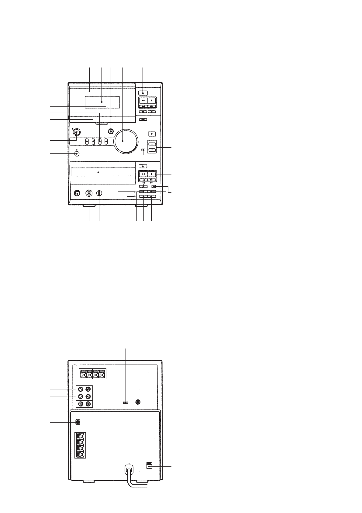
LOCATION OF CONTROLS
• Front View
2 3
1
!¶
!•
!ª
@º
@¡
@™
@£
@¢
@∞
@§
• Rear View
2
1
6
7
8
9
4 5
@¶
@• @ª
3
4
6
#º
#¡
SECTION 1
GENERAL
7
8
9
!º
!¡
!™
!£
!¢
!∞
!§
#™
1 Tape deck
2 Liquid crystal display
3 DSG button and indicator
4 VOLUME knob
5 TAPE P button
6 TAPE 6 button
7 TAPE œ, p, 0, ) buttons
8 TAPE REC r button
9 CD SYNC button and indicator
0 TUNER/BAND button
!¡ TUNING +/– buttons
!™ TUNING MODE button
!£ CD EJECT 6 button
!¢ CD ^, p, =/0, +/) buttons
!∞ CD PLAY MODE button
!§ CD REPEAT button
!¶ TUNER button and indicator
!• CD button and indicator
!ª TAPE button and indicator
@º MD/VIDEO button and indicator
@¡ 1/u button and indicator
@™ Remote sensor
@£ CD disc tray
@¢ PHONES jack
@∞ MIC IN jack
@§ MIC VOL knob
@¶ VCD ON indicator
@• PBC indicator
@ª SELECT button
#º PREV button
#¡ RETURN button
#™ NEXT button
1 AM ANTENNA terminals
2 FM ANTENNA terminals
3 SYSTEM SELECT switch
4 VIDEO OUT jack
5 POWER SELECT switch
6 LINE OUT jacks
7 MD IN jacks
8 VIDEO IN jacks
9 OPTICAL DIGITAL OUT (CD)
0 SPEAKER terminals
0
5
3
Page 4

This section is extracted from
instruction manual.
4
Page 5

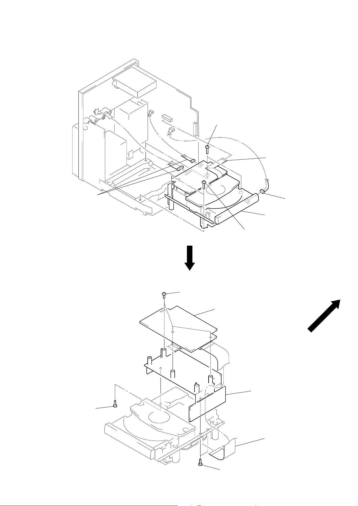
SECTION 2
s
DISASSEMBLY
Note: Follow the disassembly procedure in the numerical order given.
COVER (UPPER)
1
two case screws
3
cover (upper)
2
four screws
(BTP3
1
two case crew
×
8)
TAPE MECHANISM DECK
6
two screws
2
connector
5
tape
mechanism deck
1
flat wire (12 core)
3
two screws
(BTP3 × 8)
4
lag
3
two screws
(BTP3 × 8)
0
claw
9
F/R belt
7
motor
8
main belt
!¡
pinch roller
5
Page 6

FRONT PANEL SECTION
)
)
2
flat wire (12 core)
3
screw
(KTP3
×
6)
5
two bosses
1
connector
(CN809)
2
flat wire (20 core)
(CN804)
1
connector
2
flat wire (18 core)
(CN802)
1
connector
(CN812)
1
connector
(CN303)
6
connector (CN603
4
two screws
(BTP3
×
8)
• FRONT PANEL SECTION INSTALLATION
Note: Follow the assembly procedure in the numerical order given.
5
flat wire (12 core)
3
screw
(KTP3
×
6)
6
connector
3
screw
(KTP3
×
6)
5
flat wire (20 core)
(CN804)
7
front panel section
5
flat wire (18 core)
(CN802)
6
three connectors
(CN303, 809, 812
1
two bosses
2
connector
(CNP806)
Note: As CNP806 pin is bent easily,
4
two screws
(BTP3
3
×
8)
screw
(KTP3
×
6)
treat is carefully.
6
Page 7
CD MECHANISM DECK SECTION
)
1
two connectors
3
two screws
(BTP3 × 8)
2
flat wire (19 core)
(CN805)
1
connector
(CN306)
4
CD mechanism deck section
VCD BLOCK
2
three screws
3
VCD block
3
two screws
(BTP3 × 8)
5
holder (VCD)
4
screw
(P2
×
8)
1
flat wire (24 core
(CN701)
4
two screws
(P2
×
8)
7
Page 8

MECHANISM DECK ASS’Y
Note: As 3 coil springs are missed easily, terat them carefully.
3
coil spring
1
2
3
4
mechanism deck ass’y
two screws
×
10)
(P2.6
washer
(2130)
coil spring
(front)
(rear)
2
washer (2130)
1
two screws
(P2.6
2
washer (2130)
3
coil spring
(rear)
2
washer (2130)
3
coil spring
(front)
×
10)
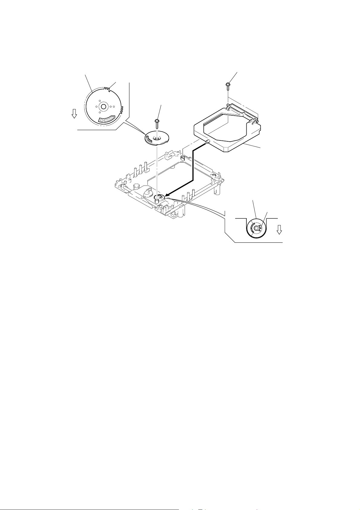
TRAY (2130)
4
Pull the tray (2130).
8
Remove the tray (2130).
1
7
lock lever
two screws
(PTPWH2.6
×
7)
2
chucking yoke (K)
6
damper (S)
A
5
claw
7
lock lever
3
Rotate the control cam
in the direction of arrow
A
.
8
Page 9
• SUB CHASSIS INSTALLATION
Note: Follow the assembly procedure in the numerical order given.
2
Install the drive gear with gear
position as shown in figure.
gear
3
screw
(PTPWH2.6 × 16)
front side
5
two screws
(PTPWH2.6 × 7)
4
sub chassis
1
Install the control cam
with gear position as shown
in figure.
gear
front side
9
Page 10

SECTION 3
SERVICE MODE
[Liquid Crystal Display All Lit Check Mode]
Procedure:
1. Set to standby state.
2. Press three buttons of p (TAPE), p (CD), and [MD/VIDEO]
simultaneously.
3. Liquid crystal display are all turned on.
4. To release from this mode, press the 1/u button to turn the
power OFF.
[Tape Deck Aging Mode]
This mode can be used for operation check of tape deck section.
Procedure:
1. Set a tape in the tape deck.
2. Set to standby state.
3. Press three buttons of p (TAPE), p (CD), and [TAPE] simultaneously.
4. The aging is executed in bellow sequence.
5. To release from the aging mode, press the 1/u button to turn
the power OFF.
Aging mode sequence:
Start
[CD Aging Mode]
This mode can be used for operation check of CD section.
Procedure:
1. Load a CD disc.
2. Set to standby state.
3. Press three buttons of p (TAPE), p (CD), and [TUNER]
simultaneously.
4. The aging is executed in bellow sequence.
5. To release from the aging mode, press the 1/u button to turn
the power OFF.
Aging mode sequence:
Start
Open the disc tray
Close the disc tray
Play the last track
FWD Play
1 minute
REC pause for 3 seconds
FWD REC
3 minutes
Fast forward
REV Play
1 minute
REC pause for 3 seconds
REV REC
3 minutes
Shut off
Shut off
Shut off
Shut off
10
Rewind
Page 11

SECTION 4
r
ELECTRICAL CONFIRMATIONS AND ADJUSTMENTS
DECK SECTION
Note: Confirm each contents of this section first of all. If the results are
not satisfied, do the adjustment.
0 dB=0.775 V
1. Demagnetize the record/playback head with a head demagnetizer.
2. Do not use a magnetized screwdriver for the adjustments.
3. After the adjustments, apply suitable locking compound to the
parts adjust.
4. The adjustments should be performed with the rated power
supply voltage unless otherwise noted.
5. The adjustments should be performed in the order given in
this service manual. (As a general rule, playback circuit adjustment should be completed before performing recording
circuit adjustment)
6. The adjustments should be performed for both L-CH and RCH.
7. Switches and controls should be set as follows unless otherwise specified.
• Test Tape
Tape Signal Used for
P-4-A100 10 kHz, –10 dB Azimuth Adjustment
P-4-L300 315 Hz, 0 dB Level Adjustment
Record/Playback Head Azimuth Adjustment
Procedure:
1. Mode: Playback
test tape
P-4-A100
(10 kHz, –10 dB)
MAIN board
LINE OUT jack (PJ301)
L-CH, R-CH
set
level mete
+
–
2. T urn the adjustment screw and check output peaks. If the peaks
do not match for L-CH and R-CH, turn the adjustment screw
so that outputs match within 1dB of peak.
Output
level
within
1dB
L-CH
peak
R-CH
peak
within
1dB
Screw
position
L-CH
peak
Screw
position
R-CH
peak
3. Mode: Playback
MAIN board
test tape
P-4-A100
(10 kHz, –10 dB)
L-CH
set
R-CH
in phase 45°90°135°180
LINE OUT jack (PJ301)
L-CH
R-CH
waveform of oscilloscope
good
oscilloscope
wrong
H
V
°
4. Repeat step 1 to 3 in playback (REV) mode.
5. After the adjustments, apply suitable locking compound to the
pats adjusted.
Adjustment Location:
reverse
forward
11
Page 12

Playback level Confirmation and Adjustment
Procedure:
Mode: Playback
test tape
P-4-L300
(315 Hz, 0 dB)
set
MAIN board
LINE OUT jack (PJ301)
L-CH, R-CH
level meter
+
–
Confirm playback level is within specification values as follows.
If these levels are out of specification values, adjust the RV151
(L-CH) and RV251 (R-CH) on the MAIN board so that the level
meter reading become within specified value.
Specified value:
PJ301 PB level: 301.5 to 338.3 mV (–8.2 to –7.2 dB) le vel dif ference between the channels: within ±0.5 dB
REC Level Confirmation and Adjustment
Procedure:
1. Mode: Record
MAIN board
MD IN jack (PJ301)
L-CH, R-CH
AF OSC
315 Hz, 50 mV (–23.8 dB)
Ω
attenuator
600
set
2. Mode: Playback
recorded
portion
set
MAIN board
LINE OUT jack (PJ301)
L-CH, R-CH
level meter
+
–
blank tape
CS-123
Adjustment Location: MAIN board
REC Bias Confirmation and Adjustment
Procedure:
1. Mode: Record
MAIN board
MD IN jack (PJ301)
L-CH, R-CH
50 mV (–23.8 dB)
600
Ω
blank tape
CN-123
set
AF OSC
1) 315 Hz
2) 10 kHz
attenuator
2. Mode: Playback
recorded
portion
set
MAIN board
LINE OUT jack (PJ301)
L-CH, R-CH
level meter
+
–
3. Confirm playback the signal recorded in step 1 become specified value as follows.
If these values are out of specification values, adjust the R V153
(L-CH) and R V253 (R-CH) on the MAIN board to repeat steps
1and 2.
3. Confirm playback the signal recorded in step 1 become specified value as follows.
If these values are out of specification v alues, adjust the R V252
(R-CH) and R V152 (L-CH) on the MAIN board to repeat steps
1 and 2.
Specified value:
PJ301 PB level: 47.2 to 53.0 mV (– 24.3 to – 23.3 dB)
Adjustment Location: MAIN board
– MAIN Board (Conductor Side) –
LINE OUT (L/R)
MD IN (L/R)
VIDEO IN (L/R)
REC Level
IC352
RV251 (R)
RV151 (L)
RV253 (R)
RV153 (L)
PJ301
RV252 (R)
RV152 (L)
Playback Level
REC Bias
Specified value: Playback output of 315 Hz to playback output
of 10 kHz: ± 0.5 dB
Adjustment Location: MAIN board
12
Page 13
CD SECTION
TP (GND)
TP (VC)
TP (FOK)
20 11
1
10
CN701
IC701
IC703
Notes:
1. CD block basically constructed to operate without adjustment. Therefore, check each item in order given.
2. Use YEDS-18 disc (Part No.: 3-702-101-01) unless otherwise indicated.
3. Use the oscilloscope with more than 10 MΩ impedance.
4. Clean an object lens by an applicator with neutral detergent when the
signal level is low than specified value with the following checks.
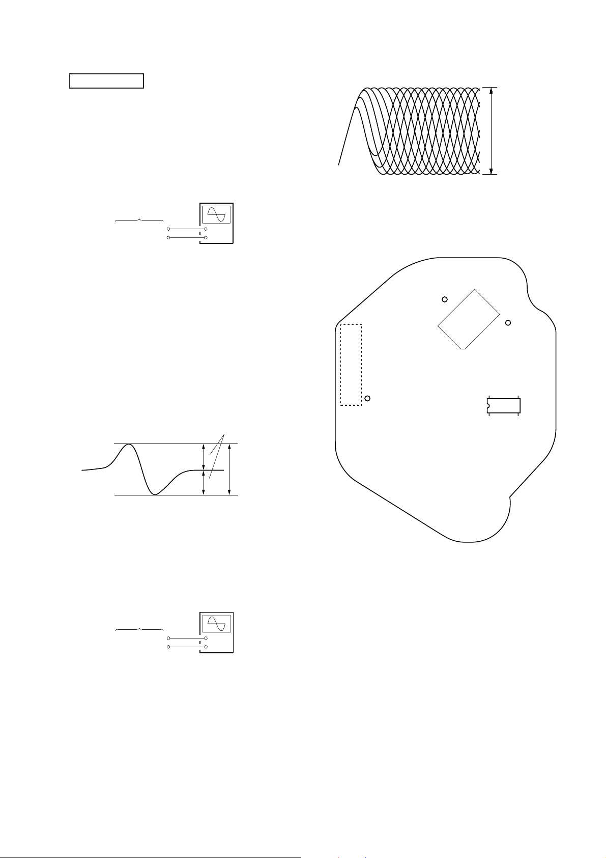
S-Curve Confirmation
Connection:
CD board
IC703 pin
!∞
TP (VC)
Procedure:
1. Connect an oscilloscope to IC703 pin !∞ and TP (VC) on the
CD board.
2. Connect between TP (FOK) and TP (GND) on the CD board
by lead wire.
3. Turn the power ON.
4. Press the
[EJECT] (CD) button to open the disc tray, and
6
put the disc (YEDS-18).
5. Press the
[EJECT] (CD) button to close the disc tray (Actu-
6
ate the focus search).
6. Conf irm that the wavef orm on the oscilloscope is symmetrical
between A and B and that peak to peak level is within 3.0 ±
1.0 Vp-p.
oscilloscope
+
–
RF signal waveform
VOLT/DIV: 200 mV
TIME/DIV: 500 ns
(with the 10: 1 probe
in use)
level: 1.3 Vp-p
+0.25
–0.20
When observing the eye pattern, set the oscilloscope for AC range
and raise vertical sensitivity.
Connecting Location:
– CD Board (Conductor Side) –
S-curve waveform
symmetry
A
within 3.0 ± 1.0 Vp-p
B
7. After confirmation, disconnect the lead wire in step 2.
Note: • Try to measure several times to make sure that the ratio of A : B
or B : A is more than 10 : 7.
• Take sweep time as long as possible and light up the brightness
to obtain best waveform.
RF Level Confirmation
Connection:
CD board
IC703 pin
TP (VC)
!§
oscilloscope
(AC range)
+
–
Procedure:
1. Connect an oscilloscope to IC703 pin !§ and TP (VC) on the
CD board.
2. Turn the power ON.
3. Load the disc (YEDS-18), and press the
back the disc.
4. Confirm that the waveform on the oscilloscope is clear and
[] button to play-
^
that the RF signal level is correct.
Note: Clear RF signal w av eform means that the shape “≈” can be clearly
distinguished at the center of the waveform.
13
Page 14

14
Page 15

5-1. BLOCK DIAGRAM – SERVO Section –
HCD-VP1
SECTION 5
DIAGRAMS
DETECTOR
A
B
C
D
F
E
OPTICAL PICK-UP
(KSS-213C/K1N)
LASER DIODE
PD
I-V AMP
10
LD
S-CLK
S-ACK
CTRL2
XTAL 16.9344MHz
AD
BCK
LRCK
GFS
C2PO
DO
RST
S-SO
S-SI
L-OUT
R-OUT
VIDEO OUT
CD L-CH
R-CH
VIDEO OUT
OPTICAL
DO
TRANSCEIVER
IC308
J401
(Page 17)
F
OPTICAL
DIGITAL OUT (CD)
IC704
6320
VCKI
XTAO
CLOCK
GENERATOR
INTERNAL BUS
DIGITAL
OUT
SBSO
75
62
XTAI
SCLK
ERROR
CORRECTOR
PEAK
DETECTOR
83
D/A DIGITAL
PROCESSOR
MUTE
79
MUTE
DATA
BCLK
LRCK
GFS
RFCK
PROCESSOR
C2PO
SERIAL/PARALLEL
DOUT
46
47
45
54
55
56
71
S-REQ
FILTER
RF AMP,
A+5V
7
4
2
1
5
6
AUTOMATIC
POWER
CONTROL
Q701
3
4
5
6
9
FOCUS/TRACKING ERROR AMP
A
B
C
D
F
8
F I-V AMP
E
E I-V AMP
1
FOCUS/TRACKING COIL DRIVE,
SPINDLE/SLED MOTOR DRIVE
LD
IC702
IC703
RF
SUMMING
AMP
APC LD
AMP
RF EQ
AMP
FOCUS
ERROR AMP
TRACKING
ERROR AMP
APC PD
AMP
RFO
RFE
FE BIAS
LDON
DIGITAL SIGNAL PROCESSOR
IC701 (1/2)
16
RF EQ
SWITCH
17
Q702
FE
15
14
TE
13
19
PD
2
RFAC
36
ASYMMETRY
CORRECTOR
ASYI
38
ASYO
39
NOISE
SHAPER
MIX
18-TIMES
OVERSAMPLING
FILTER
CLV
PROCESSOR
MDP
MON
FSW
94
97
95
96
MDS
33
31
PCO
FILO
DIGITAL PLL
VARI-PITCH
DOUBLE SPEED
SYNC
PROTECTOR
TIMING
GENERATOR 1
SCOR
XRST
74
81
WFCK
73
34
CLTV
32
FILI
TIMING
GENERATOR 2
SCOR
LDON
EFM
DEMODULATOR
ADDRESS
GENERATOR
SUBCODE Q
PROCESSOR
SUBQ
SQCK
77
78
SQCK/SCLK
REGISTER
32K
RAM
SUBQ
PRIORITY
ENCODER
SUBCODE P – W
PROCESSOR
EXCK
76
D+5V
VCD BLOCK
(1/2)
(TRACKING)
(FOCUS)
05
2-AXIS
DEVICE
M101
(SPINDLE)
M102
(SLED)
OUT+
27
M
26
16
M
17
12
13
1
2
OUT–
OUT+
OUT–
OUT–
OUT+
OUT+
OUT–
MOTOR
DRIVE
MOTOR
DRIVE
COIL
DRIVE
COIL
DRIVE
IN–
IN–
IN+
IN–
IN+
MUTE
IN+
IN+, IN–
23, 24
20
19
10
9
4
5
15
15 11
100
SW401
26
29
28
27
FE
TE
SE
RFDC
A/D
CONVERTER
SFDR
100
SRDR
2
TFDR
4
TRDR
6
FFDR
8
FRDR
10
PWM GENERATOR
FOCUS/TRACKING/SLED
SERVO DSP
FOCUS/TRACKING/SLED
SERVO
INTERFACE
COUT
89
DIGITAL SERVO
PROCESSOR
IC701 (2/2)
MIRR/DFCT/
FOK
DETECTOR
SERVO AUTO
SEQUENCER
CPU
INTERFACE
FOK
MIRR
DFCT
SENS
DATA
CLOK
XLAT
VIDEO SYSTEM
LIMIT
A +5V
93
91
92
80
86
88
87
FOK
SENS
DATA
CLK
XTL
SW-CLOSE
SW-OPEN
XRST
SYSTEM SELECT
PAL
AUTO
NTSC
S701
(LIMIT)
DISC TRAY OPEN/CLOSE
MOTOR DRIVE
IC309
IN1TR-OPEN
5 2
6 10
OUT1
IN2TR-CLOSE
OUT2
(DISC TRAY CLOSE DET)
(DISC TRAY OPEN DET)
M
M901
DISC TRAY
OPEN/CLOSE
S901
S902
17 13 12
RST
S-SO
S-CLK
S-ACK
S-REQ
SYSTEM CONTROLLER
IC801 (1/4)
S-SI
• SIGNAL PATH
: CD PLAY (AUDIO)
: CD PLAY (VIDEO)
: DIGITAL OUT
1515
Page 16
HCD-VP1
5-2. BLOCK DIAGRAM – TAPE Section –
L-CH
(RECORD/PLAYBACK)
R-CH
(ERASE)
RV253
RECORD
BIAS (R)
R-CH
R-CH
RECORD
BIAS (L)
BIAS OSC
T351
RV153
7 9
8
PLAYBACK
R-CH
REC BIAS
Q359, 360
BIAS OSC
Q357, 358
EQ AMP
IC351
REC/PB SWITCHING
IC350
SWITCH
RV151
PLAYBACK
LEVEL (L)
4
T150
BIAS
TRAP
+8V
Q351
41
39
(CrO2 DET)
DECK A/B
SELECT
N/C/M
15
BIAS SWITCH
CIRCUIT
N
C
M
25 24 23
37
REC/PB
RV152
RECORD
LEVEL (L)
DOLBY NR
AMP
CIRCUIT
33, 34
DECK PROCESS,
DOLBY NR AMP
IC352
R/MUTE
NR-ON
32
(CAPSTAN/REEL)
(TRIGGER PLUNGER)
BIAS
L/M
R/P
REC-L
35
16
17
18
20
19
M
Q352
Q353
Q354
Q356
Q355
CAPSTAN/REEL
MOTOR DRIVE
Q657, 659
TRIGGER
PLUNGER DRIVE
Q656, 658
REC-BIAS
86
REC-MUTE
87
DOLBY
88
L-MUTE
96
REC/PB
95
SYSTEM CONTROLLER
MOT-CON
10
SOL-CON
30
PB-L
REC/PB
IC801 (2/4)
A
B
C
(Page 17)
(Page 17)
(Page 18)
05
• SIGNAL PATH
: TAPE PLAY
: TAPE RECORD
16
16
(HEAD POSITION DET)
(HALF DET (SIDE-A))
(HALF DET (SIDE-B))
(CASSETTE IN DET)
TAPE END DETECT
SENSOR
1
6
32
TAPE-END
T-MODE
TC-SW
Page 17

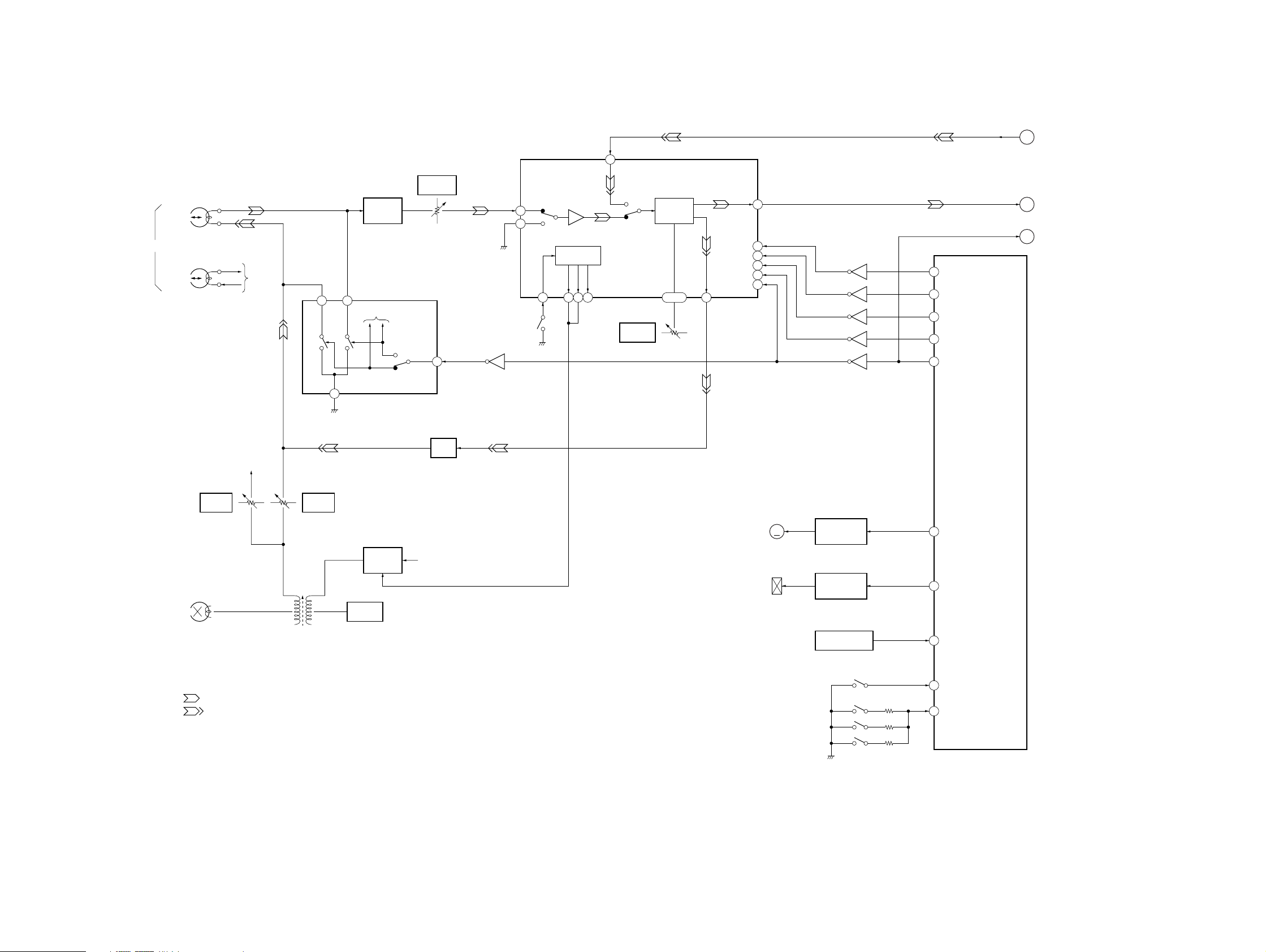
5-3. BLOCK DIAGRAM – MAIN Section –
MIC AMP
IC401
HCD-VP1
(Page 16)
VIDEO IN
(Page 18)
(Page 15)
MD IN
B
D
F
PJ301 (1/2)
L
R
L
R
PB-L
CD-ON
CD L-CH
R-CH
R-CH
D302
J402
MIC IN
MUTING
Q102, 103
R-CH
MUTING
Q106
R-CH
13 75
RV401
MIC VOL
+
INPUT SELECT SWITCH,
TONE CONTROL,
ELECTRICAL VOLUME
IC301
LIN2
12
LIN1
11
LIN4
14
LIN3
13
INPUT SELECT SWITCH
MOL
1 30
SDA
SCL
REC-L
LINE AMP
IC307
VOLUME
INL
15
SCK
28
CONTROL
16
CIRCUIT
TONE
CONTROL
CIRCUIT
ATT
LOUT
6
5
ROUT
MUTING
CONTROL SWITCH
Q317, 318
R-CH
D304
MUTING
Q101
R-CH
HEADPHONE
AMP
IC303
MUTING
Q132
R-CH
3
POWER AMP
IC101
IN+
STBY
9 10
OUT
MUTE
R-CH
R-CH
SJ301
SPEAKER
IMPEDANCE
USE 6-16Ω
14
R-CH
A
(Page 16)
L
PJ301 (2/2)
LINE OUT
R
J301
PHONES
+
L
–
–
R
+
ANTENNA
FM
75Ω
AM
TUNER PACK
FM ANT
ANT GND
ANT GND
AM ANT
L-CH
R-CH
TUNED
MD/VIDEO-ON
LINE OUT-MUTE
AMP-STBY
AMP-MUTE
11
10
DI
3
CK
4
2
CE
R-CH
Q808
Q808
TUNER ON SWITCH
4
29
19
SYSTEM CONTROLLER
TU-DATA/SDA
TU-CLK
TU-CE
IC801 (3/4)
HP-CHK
TEX
XTAL1
EXTAL1
24
MUTING
97
23
22
31
92
TX
93
40
39
CONTROL SWITCH
Q303, 304
STANDBY ON/OFF
CONTROL SWITCH
Q305, 306
MUTING
CONTROL SWITCH
Q308, 320
X802
32.768kHz
X801
4.19MHz
LED DRIVE
Q853
D853
MD/VIDEO
R-CH
R-CH
• SIGNAL PATH
: TUNER
: CD PLAY (ANALOG OUT)
: TAPE PLAY
DO
5
18
TU-COUNT
: TAPE RECORD
: MIC IN
8
9
TUNED
(Page 18)
TU-ON
E
05
1717
Page 18

HCD-VP1
5-4. BLOCK DIAGRAM – DISPLAY/POWER SUPPLY Section –
REC/PB
C
(Page 16)
RESET
54 – 85
05
50 – 53
26
27
3
21
20
36 – 33
SEG0 – SEG31
COM0 – COM3
D.S.G.
CD-SYNC
REMOCON
JOG-A
JOG-B
KEY1 – KEY4
SYSTEM CONTROLLER,
LCD DRIVER
IC801 (4/4)
TC-ON
REG-CON
TU-ON
CD-ON
VCD
PBC
LIQUID CRYSTAL
DISPLAY
LCD801
D856
DSG
D857
CD SYNC
REMOTE CONTROL
VOLUME
S801 – 822, 824-829
RECEIVER
IC802
RV801
LED DRIVE
Q856
LED DRIVE
Q857
ROTARY
ENCODER
RV801
BACK UP +5V
SYSTEM CONTROLLER (IC801) B+
38
D812
D813
98
7
25
94
8
16
LED DRIVE
Q854
LED DRIVE
Q855
LED DRIVE
LED DRIVE
LED DRIVE
Q852
Q500
Q501
D854
TAPE
D855
TUNER
D852
CD
D500
VCD ON
D501
PBC
D657 – 660
(LCD BACK LIGHT)
CASSETTE HOLDER
BACK LIGHT
REGULATOR
CONTROL SWITCH
Q315, 316
REGULATOR
CONTROL SWITCH
Q321, 322
MUTING
CONTROL SWITCH
Q311, 312
RESET SIGNAL
GENERATOR
IC803
D851
STANDBY
I/u
D858
(DISC TRAY ILLUMINATION)
TDA7439 (IC301) B+
CLOSE MOTOR DRIVER (IC306) B+
CD BLOCK B–
D815
D814
B+ SWITCH
Q653, 654
Q655
B+ SWITCH
Q651, 652
LED DRIVE
Q858
LED B+
FM 7.5V
FM CIRCUIT B+
+10V
TUNER PACK B+
+12V
+5V
CD BLOCK B+
CD BLOCK, DISC TRAY OPEN/
+8V
–5V
D802
Q859
+8V
AUDIO CIRCUIT
–8V
AUDIO
CIRCUIT
–5V
REGULATOR
IC312
D315
B+ SWITCH
Q661, 662
+7.5V
REGULATOR
Q314
+10V
REGULATOR
Q313
+5V
REGULATOR
Q310
+8V
REGULATOR
IC304
+8V
REGULATOR
IC311
–8V
REGULATOR
IC305
+12V
REGULATOR
IC306
POWER AMP
(IC101, 201)
POWER TRANSFORMER
T901
B+
B–
RECT
D907 – 910
RECT
D911 – 914
VOLTAGE
SELECTOR
S901
CD-ON
TU-ON
D
E
LINE
FILTER
LF901
(Page 17)
(Page 17)
AC IN
18
18
Page 19

HCD-VP1
5-5. NOTE FOR PRINTED WIRING BOARDS AND SCHEMATIC DIAGRAMS
Note on Printed Wiring Boards:
• X : parts extracted from the component side.
• Y : parts extracted from the conductor side.
• b : Pattern from the side which enables seeing.
Note on Schematic Diagram:
• All capacitors are in µF unless otherwise noted. pF: µµF
50 WV or less are not indicated except for electrolytics
and tantalums.
• All resistors are in Ω and 1/
specified.
• 2 : nonflammable resistor.
• C : panel designation.
Note: The components identified by mark ! or dotted line
with mark ! are critical for safety.
Replace only with part number specified.
• U : B+ Line.
• V : B– Line.
• H : adjustment for repair.
• Voltages are taken with a VOM (Input impedance 10 MΩ).
Voltage variations may be noted due to normal production tolerances.
• Waveforms are taken with a oscilloscope.
Voltage variations may be noted due to normal production tolerances.
• Circled numbers refer to waveforms.
• Signal path.
F : TUNER
E : TAPE (PLA Y)
a : TAPE (REC)
J : CD (AUDIO)
L : CD (VIDEO)
c : DIGITAL OUT
N : MIC IN
4
W or less unless otherwise
• Circuit Boards Location
CONTROL board
LOADING board
LCD board
HP/MIC board
POWER board
VIDEO SW board
MAIN board
CD board
1919
Page 20

HCD-VP1
5-6. PRINTED WIRING BOARD – CD Board – • See page 19 for Circuit Boards Location.
• Semiconductor
Location
Ref. No. Location
IC701 B-5
IC702 F-3
IC703 E-6
IC704 B-3
Q701 E-5
Q702 D-6
(Page 26)
20
20
Page 21

5-7. SCHEMATIC DIAGRAM – CD Board – • See page 31 for Waveforms. • See page 32 for IC Block Diagrams.
HCD-VP1
(Page
25)
21
21
The components identified by mark ! or dotted
line with mark ! are critical for safety.
Replace only with part number specified.
• Voltages and waveforms are dc with respect to ground
under no-signal conditions.
no mark : CD PLAY
: Impossible to measure
∗
Page 22

HCD-VP1
5-8. SCHEMATIC DIAGRAM – MAIN Board (1/4) – • See page 34 for IC Block Diagram.
(Page
24)
(Page 25)
(Page
25)
(Page 25)
(Page 23)
• Voltages and waveforms are dc with respect to ground
under no-signal (detuned) conditions.
no mark : FM
( ) : CD PLAY
[ ] : TAPE PLAY
〈〈 〉〉 : MD/VIDEO
22
22
Page 23

5-9. SCHEMATIC DIAGRAM – MAIN Board (2/4), HP/MIC Board, VIDEO SW Board, LOADING Board – • See page 34 for IC Block Diagrams.
HCD-VP1
(Page
22)
(Page 30)
(Page 25)
23
23
(Page 25)
The components identified by mark ! or dotted
line with mark ! are critical for safety.
Replace only with part number specified.
• Voltages and waveforms are dc with respect to ground
under no-signal (detuned) conditions.
no mark : FM
( ) : CD PLAY
[ ] : TAPE PLAY
〈〈 〉〉 : MD/VIDEO
Page 24

HCD-VP1
5-10. SCHEMATIC DIAGRAM – MAIN Board (3/4) – • See page 31 for Waveforms.
(Page 22)
(Page 25)
(Page
25)
24
• Voltages and waveforms are dc with respect to ground
under no-signal conditions.
no mark : TAPE PLAY
( ) : TAPE REC
24
Page 25

5-11. SCHEMATIC DIAGRAM – MAIN Board (4/4), LCD Board – • See page 31 for Waveforms.
(Page 24)
HCD-VP1
(Page 29)
(Page 29)
(Page
21)
(Page 23)
(Page 22)
(Page 24)
(Page 23)
(Page 22)
(Page 22)
25
25
Page 26

HCD-VP1
5-12. PRINTED WIRING BOARD – MAIN Board – • See page 19 for Circuit Boards Location.
(Page 27) (Page 27) (Page 28)
(Page 28)
(Page 27)
(Page 20)
(Page 27)
26
26
(Page 30) (Page 27)
Page 27

5-13. PRINTED WIRING BOARDS – LCD Board, HP/MIC Board, VIDEO SW Board, LOADING Board – • See page 19 for Circuit Boards Location.
HCD-VP1
(Page 26)
• Semiconductor Location
– MAIN Board –
Ref. No. LocationRef. No. Location
D301 D-8
D302 D-9
D304 C-8
D314 I-5
D315 I-6
D317 B-8
D319 B-7
D323 D-8
D350 E-5
D351 F-5
D352 E-4
D353 E-3
D354 E-5
D361 F-4
D362 G-3
D651 D-1
D652 D-2
D801 F-1
D802 F-1
D812 B-2
D813 C-1
D814 A-2
D815 F-1
IC101 F-8
IC201 H-8
IC301 D-7
IC303 F-6
IC304 I-7
IC305 H-4
IC306 I-7
IC307 C-8
IC308 E-9
IC309 D-3
IC311 I-6
IC312 G-4
IC350 H-2
IC351 G-2
IC352 F-3
IC801 B-3
IC803 B-4
Q101 C-9
Q102 D-9
Q103 D-9
Q106 E-6
Q201 B-9
Q202 E-9
Q203 D-9
Q206 E-7
Q303 C-8
Q304 C-8
Q305 F-7
Q306 F-7
Q308 F-7
Q310 I-5
Q311 D-9
Q312 H-4
Q313 B-8
Q314 B-7
Q315 B-7
Q316 B-7
Q317 E-6
Q318 E-6
Q320 F-7
Q321 B-8
Q322 B-8
Q351 E-4
Q352 E-3
Q353 E-3
Q354 E-3
Q355 E-4
Q356 E-4
Q357 I-3
Q358 I-2
Q359 I-1
Q360 H-2
Q651 B-1
Q652 B-1
Q653 B-2
Q654 B-1
Q655 B-1
Q656 D-3
Q657 D-3
Q658 D-3
Q659 D-3
Q661 C-2
Q662 C-2
Q808 B-6
(Page 26)
LOADING BOARD
05
M901
DISC TRAY
OPEN/CLOSE
M
(Page 26) (Page 26)
S901
DISC TRAY
CLOSE DET
S902
DISC TRAY
OPEN DET
1-640-523-
CN900
1
5
(Page 26)
G
11
27
27
Page 28

HCD-VP1
• Semiconductor
Location
Ref. No. Location
D500 H-2
D501 H-2
D851 C-7
D852 D-5
D853 D-6
D854 D-6
D855 D-5
D856 C-4
D857 B-2
D858 F-5
IC802 E-7
Q500 H-2
Q501 H-2
Q852 D-5
Q853 D-7
Q854 D-6
Q855 D-5
Q856 C-4
Q857 C-2
Q858 C-7
Q859 D-7
5-14. PRINTED WIRING BOARD – CONTROL Board – • See page 19 for Circuit Boards Location.
(Page 26)
28
(Page 26)
28
Page 29

5-15. SCHEMATIC DIAGRAM – CONTROL Board –
HCD-VP1
(Page 25)
(Page 25)
29
• Voltages and waveforms are dc with respect to ground
under no-signal (detuned) conditions.
no mark : FM
29
Page 30

HCD-VP1
5-16. PRINTED WIRING BOARD – POWER Board – • See page 19 for Circuit Boards Location.
• Semiconductor
Location
Ref. No. Location
D907 C-3
D908 C-3
D909 C-3
D910 D-3
D911 A-2
D912 A-2
D913 A-3
D914 A-3
5-17. SCHEMATIC DIAGRAM – POWER Board –
(Page 26)
(Page 23)
The components identified by mark ! or dotted
line with mark ! are critical for safety.
Replace only with part number specified.
30
30
Page 31

• Waveforms
– CD Board –
– MAIN Board –
1 IC703 !£ (TE) (CD play mode)
2 IC703 !∞ (FE) (CD play mode)
3 IC703 !§ (RFO) (CD play mode)
430 mVp-p
170 mVp-p
6 IC701 %∞ (RFCK)
136 µs
7 IC701 ^™ (XTAI)
16.9344 MHz
8 IC701 &£ (WFCK)
5.6 Vp-p
5.2 Vp-p
1 Q357, 358 collector (REC mode)
13.6 Vp-p
11.6 µs
2 Q360 collector (REC mode)
0.5 Vp-p
11.6 µs
3 IC801 (£ (TEX)
4 IC701 $∞ (LRCK)
22.8 µs
5 IC701 $¶ (BCLK)
1.3 Vp-p
0.8 Vp-p
5.1 Vp-p
136 µs
9 IC701 (§ (MDP) (CD play mode)
µ
s
7.6
5.6 Vp-p
2.6 Vp-p
2.4 Vp-p
32.768 kHz
4 IC801 $º (XTAL1)
5.2 Vp-p
4.19 MHz
470 ns
31
Page 32

• IC Block Diagrams
– CD Board –
IC701 CXD2545Q
SBSO
EXCK
SQSO
SQCK
MUTE
SENS
XRST
DIRC
SCLK
DFSW
ATSK
DATA
XLAT
CLOK
COUT
ADD
MIRR
DFCT
FOK
FSW
MON
MDP
MDS
LOCK
SSTP
76
77
78
79
80
81
82
83
84
85
86
87
88
89
90
91
92
93
94
95
96
97
98
99
P-W
SUBCODE
PROCESSOR
Q
SUBCODE
PROCESSOR
CPU
CPU
INTERFACE
INTERFACE
SERVO
AUTO
SEQUENCER
SCOR
TIMING
SERVO
INTERFACE
MICRO PROGRAM
CLV
WFCK
EMPH
SYNC
GENERATOR 1
32K RAM
CPU
ADDRESS
INTERFACE
GENERATOR
NOISE
PROCESSOR
PROTECTOR
D/A
DIGITAL
PROCESSOR
CPU
PRIORITY
ENCODER
INTERFACE
SHAPER
D OUT
OUT
DIGITAL
PEAK
RESISTER
CPU
ERROR
INTERFACE
CORRECTOR
FILTER
18-TIMES
OVER SAMPLING
MD2
C16M
DETECTOR
CPU
TIMING
FSTI
FSTO
C4M
CLOCK
GENERATOR
INTERFACE
GENERATOR 2
3
DVSS
XTAI
XTAO
XTSL
6263646566676869707172737475
EFM
CPU
INTERFACE
DEMODULATOR
PLL
DIGITAL
VARI-PITCH
DA01|DA11
61 – 51
SERIAL
PARALLEL
MUX
CPU
ASYMMETRY
DOUBLE SPEED
46
|
50
45
44
43
PROCESSOR
42
41
40
39
38
INTERFACE
37
CORRECTION
36
35
34
33
32
31
DA16
|
DA12
LRCK
WDCK
PSSL
ASYE
ADD
AVDD
ASYO
ASYI
BIAS
RFAC
AVSS
CLTV
PCO
FILI
FILO
SFDR
32
SLED
SERVO
TRACKING
SLED PWM
GENERATOR
TRACKING PWM
100
2 345 6 7 8 9 10 11 201918171615141312
1
TFDR
SFON
SRDR
TRON
SRON
SERVO
GENERATOR
FFDR
TFON
TRDR
FOCUS
SERVO
GENERATOR
FOCUS PWM
FFON
FRON
FRDR
SERVO DSP
PWM GENERATOR
VCO0
VCO1
TEST
MIRR
DVSS
DFCT
TES2
FOK DETECTOR
PDO
TES3
VPCO
VCKI
4
A/D
SWITCH
CONVERTER
21 22 23 24 25
IGEN
ADIO
AVSS
AVDD
&
BUFFER
RFC
VC
30
FE
29
SE
28
TE
27
26
RFDC
Page 33

IC702 BA6392FP-E2
BUFF
1CH1 OUT F
BUFF
2CH1 OUT R
3CAPA IN 1
R
4CH1 R IN
INTERFACE
F
5CH1 F IN
6VREF IN
BUFF
F
R
LEVEL
SHIFT
28 GND
BUFF
27 CH4 OUT F
26 CH4 OUT R
BUFF
25 VB IN
24 VS IN
23 VB IN
7VREF OUT
8GND
FF
9CH2 F IN
INTERFACE INTERFACE
RR
10CH2 R IN
11CAPA IN 2
BUFF BUFF
12CH2 OUT R
BUFF
13CH2 OUT F
14GND
RRFF
BUFF
MUTE
IC703 CXA1821M-T6
1
LD VCCVCC
2
PD LD ON
VCC
20
19
22 VCC
21 VCC
20 CH3 F IN
19 CH3 R IN
18 CAPA IN 3
17 CH3 OUT R
16 CH3 OUT F
15 MUTE
3
A LC/PD
VEE
VEE
VC
RF SUMMING AMP
4
B RFE
5
C RFO
6
D FE
7
VEE FE BIAS
VC
8
F TE
9
E VC
EI EO
VC
10
VREF
VC
APC LD AMP
VEE
TRACKING ERROR AMP
VC
VC
VCC
VEE
RF EQ AMP
VC
FOCUS ERROR AMP
VC BUFFER
18
17
16
15
14
13
VC
12
11
33
Page 34

– MAIN Board –
IC101, 201 TDA7296
BIPOLAR
TRANSCONDACTANCE
INPUT STAGE
–
+
IN–
IN+
STBY-GND
IN+ MUTE
IC301 TDA7439
SCL
DIG GND
TREBLE (R)
TREBLE (L)
MIN (L)
NC
MOUT (L)
BOUT (L)
LEVEL SHIFTING
BIN (L)
BOUT (R)
MOS GAIN &
STAGE
BOOST-
STRAP
BOOSTSTRAP
BIN (R)
MOUT (R)
MIN (R)
+VS
STANDBY/
MUTE
–VS
STBY
INR
18
VOLUME
TREBLE
THERMAL
SHUTDOWN
MOS
OUTPUT
STAGE
MUTE
SHORT
CIRCUIT
PROTECTION
NC
NC
MUX OUT (R)
14 1512 1310 118 96 753 41 2
OUT
+PWVS
–PWVS
INL
161727282930 22 21 20 1926 25 24 23
VOLUME
TREBLE
IIC BUS
DECODER &
LATCH
VREF
SUPPLY
1 2 3 4 5 6
CREF
VS
AGND
SDA
IC305 KA7908
DRIVER OUT
ROUT
LOUT
MIDDLE
BASS
SPEAKER
ATTENUATOR
GAIN AMP
MULTIPLEXER
7 8
9 10
R-IN4
R-IN3
R-IN2
11 12
R-IN1
MIDDLE
BASS
SPEAKER
ATTENUATOR
GAIN AMP
MULTIPLEXER
13 14
L-IN1
L-IN2
L-IN3
15
L-IN4
MUX OUT (L)
34
BIAS
GND
OUT1
VZ1
PRE DRIVER
LOGIC
SWITCH
5 6 7 8 9 101 2 3 4
IN1
VCTL
IN2
VCC1
TSD
VCC2
VZ2
OUT2
Page 35

5-18. IC PIN FUNCTION DESCRIPTION
• MAIN BOARD IC801 CXP83120A-132Q (SYSTEM CONTROLLER, LCD DRIVER)
Pin No. Pin Name I/O Description
1 TAPE-END I
2
3 REMOCON I
4 TU-DATA/SDA O
5
6 T-MODE I
7 REG-CON O
8
9
10
11
12
13
14
15
16
17
18
19
20 JOG-B I
21 JOG-A I
22
23
24
25 TU-ON O
26 D.S.G. O
27 CD-SYNC O
28
29
30 SOL-CON O
31
32 TC-SW I
33 KEY4 I
34 KEY3 I
35 KEY2 I
36 KEY1 I
37 SIMUKE I
GND
NC
VCD
TUNED
MOT-CON
S-CLK
S-SI
S-SO
CD-MUTE
S-REQ
PBC
RST
TU-COUNT
TU-CE
AMP-MUTE
AMP-STBY
MD/VIDEO-ON
SCK
TU-CLK
HP-CHK
Tape end detect sensor input terminal “H” input when the tape end detected
—
Ground terminal
Sircs remote control signal input from the remote control receiver (IC802)
PLL serial data output to PLL IC on the tuner pack (at tuner function)
2
C data output to the TDA7439 (IC301) (all functions)
I
—
Not used (open)
Head position detect switch input terminal “L”: forward direction, “H”: reverse direction
Main system power supply on/off control signal output terminal “H”: power on
O
LED drive signal output of the VCD ON indicator (D500) “H”: LED on
I
Tuning detection signal input from the tuner pack “L”: tuned
O
Capstan/reel motor on/off control signal output terminal “H”: motor on
O
Serial data transfer clock signal output to the VCD block (at CD function)
I
Serial data input from the VCD block (at CD function)
O
Serial data output to the VCD block (at CD function)
O
Not used (open)
O
Interrupt status output to the VCD block
O
LED drive signal output of the PBC indicator (D501) “H”: LED on
O
Reset signal output to the VCD block “L”: reset
I
PLL count data input from PLL IC on the tuner pack (at tuner function)
O
PLL serial chip enable signal output to PLL IC on the tuner pack (at tuner function)
Jog dial pulse input from the rotary encoder (RV801 VOLUME) (B phase input)
Jog dial pulse input from the rotary encoder (RV801 VOLUME) (A phase input)
Muting on/off control signal output to the power amplifier (IC101, 201)
O
“H”: muting on
Standby on/off control signal output to the power amplifier (IC101, 201)
O
“L”: standby mode
MD/VIDEO function control signal output terminal
O
“H”: MD/VIDEO (“L” output when other functions)
Power supply on/off control signal output of the tuner pack (TU +10V and FM +7.5V)
LED drive signal output of the TUNER indicator (D855) “H”: tuner power on (LED on)
LED drive signal output of the DSG (Dynamic Sound Generator) indicator (D856)
“H”: LED on
LED drive signal output of the CD SYNC indicator (D857) “H”: LED on
O
Serial data transfer clock signal output to the TDA7439 (IC301)
O
PLL serial data transfer clock signal output to PLL IC on the tuner pack (at tuner function)
Trigger plunger on/off control signal output terminal “H”: plunger on
I
Headphone check detection signal input terminal
Half detect (side A and B) switch and cassette in detect switch input terminal (A/D input)
Key input terminal (A/D input) S826 to S829 (SELECT, PREV, NEXT, RETURN keys input)
Key input terminal (A/D input) S817 to S822, S824 and S825 (STANDBY I/u, CD, TUNER,
TAPE, MD/VIDEO, DSG, TUNER BAND, CD SYNC keys input)
Key input terminal (A/D input) S801 to S808 (TUNING MODE, CD ^/p/+/=, PLAY
MODE, REPEAT, CD EJECT 6 keys input)
Key input terminal (A/D input)
S809 to S816 (TAPE 9 (/p/)/0/P, REC r, TUNING +/– keys input)
Destination setting terminal (A/D input)
35
Page 36

Pin No. Pin Name I/O Description
38 RESET I
39
40
41 VSS —
42 XTAL2 O
43
44 AVREF I
45 AVSS —
46
47 to 49
50 to 53 COM0 to COM3 O
54 to 85 SEG0 to SEG31 O
86 REC-BIAS O
87 REC-MUTE O
88 DOLBY O
89 VDD —
90 NC —
91 VSS —
92
93
94 CD-ON O
95 REC/PB O
96 L-MUTE O
97
98 TC-ON O
99 WP I
100
EXTAL1
XTAL1
EXTAL2
VL
VLC3 to VLC1
TX
TEX
LINE OUT-MUTE
S-ACK
System reset signal input from the reset signal generator (IC803) “L”: reset
For several hundreds msec. after the power supply rises, “L” is input, then it changes to “H”
I
Main system clock input terminal (4.19 MHz)
O
Main system clock output terminal (4.19 MHz)
Ground terminal
Sub system clock output terminal (500 kHz) Not used (open)
I
Sub system clock input terminal (500 kHz) Not used (fixed at “L”)
Reference voltage (+5V) input terminal (for A/D conversion)
Ground terminal (for A/D conversion)
O
Liquid crystal display bias on/off control signal output terminal
—
Power supply terminal for the liquid crystal display bias
Common drive signal output to the liquid crystal display (LCD801)
Segment drive signal output to the liquid crystal display (LCD801)
Recording bias on/off selection signal output to the HA12203NT (IC352)
“L”: bias on, “H”: bias off
Recording muting on/off selection signal output to the HA12203NT (IC352)
“L”: muting on, “H”: muting off
Dolby NR on/off selection signal output to the HA12203NT (IC352)
“L”: dolby on, “H”: dolby off
Power supply terminal (+5V)
Connected to power supply (+5V)
Ground terminal
O
Sub system clock output terminal (32.768 kHz)
I
Sub system clock input terminal (32.768 kHz)
LED drive signal output of the CD indicator (D852) “H”: CD power on (LED on)
Recording/playback selection signal output to the BA3126N (IC350) and HA12203NT (IC352)
“L”: playback mode, “H”: recording mode
Line muting on/off selection signal output to the HA12203NT (IC352)
“L”: muting on, “H”: muting off
O
Muting on/off control signal output terminal “H”: muting on
Power supply on/off control signal output of the cassette holder back light
LED drive signal output of the TAPE indicator (D854) “H”: back light on (LED on)
Wakeup control signal input terminal
I
Subcode sync (S0+S1) detection signal input from the VCD block (at CD function)
36
Page 37

SECTION 6
EXPLODED VIEWS
NOTE:
• -XX and -X mean standardized parts, so they
may have some difference from the original
one.
• Color Indication of Appearance Parts
Example:
KNOB, BALANCE (WHITE) . . . (RED)
↑↑
Parts Color Cabinet's Color
• Abbreviation
CH : Chinese model HK : Hong Kong model
MY : Malaysia model SP : Singapore model
TH : Thai model
• Items marked “*” are not stocked since they
are seldom required for routine service. Some
delay should be anticipated when ordering
these items.
• The mechanical parts with no reference number in the exploded views are not supplied.
• Hardware (# mark) list is given in the last of
the electrical parts list.
(1) COVER, TAPE MECHANISM DECK SECTION
6
#1
not
supplied
The components identified by
mark ! or dotted line with mark
! are critical for safety.
Replace only with part number
specified.
#1
not
supplied
3
1
#2
7
5
4
6
#1
2
#1
not
supplied
Chassis section
Front panel
secrtion
#1
Ref. No. Part No. Description Remark
1 1-772-001-11 ELECTRIC, MECHANICAL (TAPE DECK BLOCK)
2 X-4949-568-1 ROLLER PINCH BLK R ASSY
3 X-4949-569-1 ROLLER PINCH BLK L ASSY
4 4-997-984-01 BELT, F/R
#2
Ref. No. Part No. Description Remark
5 4-997-983-01 BELT, MAIN
6 4-221-580-01 SCREW, CASE
* 7 4-217-341-01 COVER (UPPER)
37
Page 38

(2) FRONT PANEL SECTION
54
53
55
57
56
52
supplied with RV801
60
61
58
59
#3
62
63
69
73
#1
#1
64
64
not
supplied
64
65
72
64
67
51
Ref. No. Part No. Description Remark
51 X-4951-108-1 KNOB ASSY
52 X-4951-938-1 PANEL SUB ASSY, FRONT
53 4-222-321-01 WINDOW (CASSETTE)
54 4-217-356-01 SHEET (WINDOW), ADHESIVE
55 4-217-316-01 LID, CASSETTE
56 1-675-188-11 LCD BOARD
57 4-217-319-01 PLATE, LCD LIGHT
58 4-217-317-01 HOLDER (CASSETTE)
59 4-217-345-01 SPRING, CASSETTE
60 1-790-628-11 WIRE (FLAT TYPE) (18 CORE)
61 1-790-629-11 WIRE (FLAT TYPE) (20 CORE)
66
not supplied
#1
70
71
Ref. No. Part No. Description Remark
62 1-418-482-11 ILLUMINATION BLOCK, LED
63 X-4951-937-1 LOCK (EJECT) ASSY
64 4-931-757-31 SCREW (DIA. 2.6X8) (IT3B), TAPPING
65 4-222-083-01 CUSHION (DSG)
66 4-221-075-01 KNOB (MIC VOL)
67 A-4426-610-A CONTROL BOARD, COMPLETE
69 3-351-377-11 GEAR, DAMPER
70 4-218-204-01 FOOT (FRONT)
71 1-675-190-11 HP/MIC BOARD
72 4-219-810-01 RUBBER (SPACE)
73 1-675-192-11 VIDEO SW STOPPER BOARD
38
Page 39

(3) CHASSIS SECTION
115
123
#7
104
KSL-2130CCP/K1N
#1
126
#7
#1
122
not
supplied
105
#4
120
#1
116
T901
not
supplied
TH, CHMY, SP, HK HK
116
#4
118
112
115
121
#1
117
119
not
supplied
106
#1
#1
#1
not
supplied
124
111
125
109
Ref. No. Part No. Description Remark
104 4-222-428-01 LID, CD
105 1-675-187-11 POWER BOARD
106 4-217-338-31 PANEL, BACK
107 A-4426-615-A MAIN BOARD, COMPLETE
* 108 4-217-354-01 BUSHING, INSULATING
109 4-217-355-01 FOOT
110 1-790-630-11 WIRE (FLAT TYPE) (12 CORE)
111 3-703-244-00 BUSHING (2104), CORD (CH)
111 3-703-571-11 BUSHING (S) (4516), CORD (TH)
111 4-217-350-01 STOPPER, CORD (MY, SP, HK)
110
#1
115
108
#1
107
The components identified by mark ! or dotted
line with mark ! are critical for safety.
Replace only with part number specified.
Ref. No. Part No. Description Remark
! 116 1-696-169-21 CORD, POWER (MY, SP, HK)
! 116 1-783-205-11 CORD, POWER (CH)
! 117 1-770-019-11 ADAPTOR, CONVERSION PLUG 3P (HK)
118 3-911-135-01 SCREW (2.6X10), (+PWH) TAPPING
119 1-675-191-11 VIDEO SW BOARD
120 4-220-971-01 RUBBER (POWER)
121 1-675-192-11 VIDEO SW STOPPER BOARD
122 1-791-494-11 WIRE (FLAT TYPE) (24 CORE)
123 1-791-493-11 WIRE (FLAT TYPE) (19 CORE)
124 4-217-337-01 CHASSIS (CD)
112 A-4426-617-A TUNER PACK
115 4-931-757-31 SCREW (DIA. 2.6X8) (IT3B), TAPPING
! 116 1-558-943-31 CORD, POWER (TH)
125 4-217-342-03 CHASSIS (LOWER)
126 1-761-268-11 BOARD, UNIT (VCD BLOCK)
! T901 1-433-809-11 TRANSFORMER, POWER
39
Page 40

(4) CD MECHANISM DECK SECTION-1
(KSL-2130CCP/K1N)
not
supplied
not
supplied
156
155
154
153
157
161
158
160
not
supplied
not
supplied
159
157
162
not
supplied
151
152
164
165
169
167
#5
Ref. No. Part No. Description Remark
* 151 2-646-290-01 TRAY (2130)
152 2-625-541-02 DAMPER (S)
153 2-625-279-01 SCREW (B 2.6X2.5), +
154 2-625-274-02 GEAR, MIDWAY
155 2-625-276-02 PULLEY, LOADING
156 3-653-387-00 BELT, LM
157 2-626-294-01 SCREW (+PTPWH) (2.6X7)
* 158 2-625-284-05 PLATE, CHUCKING
159 1-452-493-21 MAGNET
160 2-625-286-03 PULLEY, CHUCKING
M901
163
165
166
167
#5
Ref. No. Part No. Description Remark
161 3-319-501-51 SCREW (+PTPWH) (2.6X16)
* 162 2-646-288-01 CHASSIS (2130), SUB
* 164 1-640-523-11 LOADING BOARD
* 165 2-627-234-01 INSULATOR
166 2-627-235-01 SPRING (REAR), COIL
167 2-646-289-01 WASHER (2130)
168 2-641-386-01 SCREW (2X5), TAPPING (S)
169 2-627-236-01 SPRING (FRONT), COIL
M901 X-2625-117-1 MOTOR ASSY, LOADING
40
Page 41

(5) CD MECHANISM DECK SECTION-2
(KSL-2130CCP/K1N)
not supplied
203
M102
207
208
205
206
not supplied
202
M101
201
Ref. No. Part No. Description Remark
201 A-4426-613-A CD BOARD, COMPLETE
202 2-625-188-02 GEAR (A)
203 2-627-003-02 GEAR (B) (RP)
204 1-791-495-11 WIRE (FLAT TYPE) (16 CORE)
205 2-626-908-01 SHAFT, SLED
204
#6
The components identified by mark ! or dotted
line with mark ! are critical for safety.
Replace only with part number specified.
Ref. No. Part No. Description Remark
! 206 8-820-070-02 OPTICAL PICK-UP KSM-213CCP/K1N
207 3-713-786-51 SCREW +P 2X3
206 2-641-386-01 SCREW (2X5), TAPPING (S)
M101 X-2646-381-1 MOTOR CHASSIS ASSY (MB) (SPINDLE)
M102 X-2625-769-1 MOTOR GEAR ASSY (MB) (RP) (SLED)
41
Page 42

CD
SECTION 7
ELECTRICAL PARTS LIST
NOTE:
• Due to standardization, replacements in the
parts list may be different from the parts specified in the diagrams or the components used
on the set.
• -XX and -X mean standardized parts, so they
may have some difference from the original
one.
• RESISTORS
All resistors are in ohms.
METAL: Metal-film resistor.
METAL OXIDE: Metal oxide-film resistor.
F: nonflammable
• Abbreviation
CH : Chinese
HK : Hong Kong
MY : Malaysia
Ref. No. Part No. Description Remark Ref. No. Part No. Description Remark
A-4426-613-A CD BOARD, COMPLETE
C701 1-163-005-11 CERAMIC CHIP 470PF 10% 50V
C702 1-115-339-11 CERAMIC CHIP 0.1uF 10% 50V
C703 1-163-197-00 CERAMIC CHIP 470PF 10% 50V
C705 1-126-157-11 ELECT 10uF 20% 16V
C706 1-164-346-11 CERAMIC CHIP 1uF 16V
C707 1-164-346-11 CERAMIC CHIP 1uF 16V
C708 1-115-339-11 CERAMIC CHIP 0.1uF 10% 50V
C709 1-163-011-11 CERAMIC CHIP 0.0015uF 10% 50V
C710 1-163-055-00 CERAMIC CHIP 0.0047uF 10% 50V
C711 1-163-251-11 CERAMIC CHIP 100PF 5% 50V
C712 1-115-339-11 CERAMIC CHIP 0.1uF 10% 50V
C713 1-115-339-11 CERAMIC CHIP 0.1uF 10% 50V
C715 1-124-589-11 ELECT 47uF 20% 16V
C716 1-124-589-11 ELECT 47uF 20% 16V
C717 1-113-500-11 TANTALUM CHIP 100uF 20% 10V
C718 1-163-009-11 CERAMIC CHIP 0.001uF 10% 50V
C719 1-163-102-00 CERAMIC CHIP 24PF 5% 50V
C720 1-115-339-11 CERAMIC CHIP 0.1uF 10% 50V
C723 1-163-021-11 CERAMIC CHIP 0.01uF 10% 50V
C724 1-107-823-11 CERAMIC CHIP 0.47uF 10% 16V
C725 1-126-157-11 ELECT 10uF 20% 16V
C741 1-115-339-11 CERAMIC CHIP 0.1uF 10% 50V
C742 1-115-339-11 CERAMIC CHIP 0.1uF 10% 50V
C751 1-163-167-00 CERAMIC CHIP 27PF 5% 50V
C753 1-115-339-11 CERAMIC CHIP 0.1uF 10% 50V
SP : Singapore
TH : Thai
*******************
< CAPACITOR >
• Items marked “*” are not stocked since they
are seldom required for routine service.
Some delay should be anticipated when ordering these items.
• SEMICONDUCTORS
In each case, u: µ, for example:
uA. . : µA. . uPA. . : µPA. .
uPB. . : µPB. . uPC. . : µPC. .
uPD. . : µPD. .
• CAPACITORS
uF: µF
• COILS
uH: µH
* IC702 8-759-455-91 IC BA6392FP-E2
IC703 8-752-072-45 IC CXA1821M-T6
IC704 8-759-271-86 IC TC7SH04F (TE85R)
JR701 1-216-295-00 SHORT 0
JR702 1-216-295-00 SHORT 0
JR703 1-216-295-00 SHORT 0
JR704 1-216-295-00 SHORT 0
JR705 1-216-295-00 SHORT 0
JR706 1-216-296-00 SHORT 0
JR707 1-216-296-00 SHORT 0
JR708 1-216-296-00 SHORT 0
JR709 1-216-296-00 SHORT 0
JR710 1-216-296-00 SHORT 0
JR711 1-216-296-00 SHORT 0
JR712 1-216-296-00 SHORT 0
JR713 1-216-296-00 SHORT 0
JR714 1-216-296-00 SHORT 0
JR715 1-216-296-00 SHORT 0
JR716 1-216-296-00 SHORT 0
JR717 1-216-296-00 SHORT 0
JR718 1-216-296-00 SHORT 0
JR719 1-216-296-00 SHORT 0
JR720 1-216-296-00 SHORT 0
JR721 1-216-296-00 SHORT 0
JR723 1-216-295-00 SHORT 0
The components identified by
mark ! or dotted line with mark
! are critical for safety.
Replace only with part number
specified.
When indicating parts by reference
number, please include the board.
< SHORT >
< TRANSISTOR >
C754 1-162-568-11 CERAMIC CHIP 0.33uF 25V
C756 1-163-167-00 CERAMIC CHIP 27PF 5% 50V
C757 1-163-209-00 CERAMIC CHIP 0.0015uF 5% 50V
C759 1-163-019-00 CERAMIC CHIP 0.0068uF 10% 50V
C761 1-163-077-00 CERAMIC CHIP 0.1uF 10% 25V
C762 1-163-009-11 CERAMIC CHIP 0.001uF 10% 50V
C763 1-126-925-11 ELECT 470uF 20% 10V
< CONNECTOR >
CN702 1-770-674-11 CONNECTOR, FFC/FPC 16P
< IC >
IC701 8-752-369-78 IC CXD2545Q
42
Q701 8-729-010-08 TRANSISTOR MSB710-RT1
Q702 8-729-120-28 TRANSISTOR 2SC1623-T1-L5L6
< RESISTOR >
R701 1-216-077-00 RES, CHIP 15K 5% 1/10W
R702 1-216-097-00 RES, CHIP 100K 5% 1/10W
R703 1-216-226-00 RES, CHIP 15K 5% 1/8W
R704 1-216-085-00 METAL CHIP 33K 5% 1/10W
R705 1-216-097-00 RES, CHIP 100K 5% 1/10W
R706 1-216-049-11 RES, CHIP 1K 5% 1/10W
R707 1-216-049-11 RES, CHIP 1K 5% 1/10W
R708 1-216-210-00 RES, CHIP 3.3K 5% 1/8W
R709 1-216-121-00 RES, CHIP 1M 5% 1/10W
R710 1-216-174-00 RES, CHIP 100 5% 1/8W
Page 43

CD CONTROL
Ref. No. Part No. Description Remark
R712 1-216-049-11 RES, CHIP 1K 5% 1/10W
R723 1-216-073-00 METAL CHIP 10K 5% 1/10W
R724 1-216-097-00 RES, CHIP 100K 5% 1/10W
R725 1-216-033-00 METAL CHIP 220 5% 1/10W
R726 1-216-033-00 METAL CHIP 220 5% 1/10W
R727 1-216-033-00 METAL CHIP 220 5% 1/10W
R731 1-216-037-00 METAL CHIP 330 5% 1/10W
R734 1-216-049-11 RES, CHIP 1K 5% 1/10W
R741 1-216-089-00 RES, CHIP 47K 5% 1/10W
R742 1-216-230-00 RES, CHIP 22K 5% 1/8W
R743 1-216-101-00 METAL CHIP 150K 5% 1/10W
R744 1-216-250-00 RES, CHIP 150K 5% 1/8W
R746 1-216-073-00 METAL CHIP 10K 5% 1/10W
R747 1-216-067-00 METAL CHIP 5.6K 5% 1/10W
R748 1-216-001-00 METAL CHIP 10 5% 1/10W
R749 1-216-003-11 RES, CHIP 12 5% 1/10W
R750 1-216-025-00 RES, CHIP 100 5% 1/10W
R751 1-216-174-00 RES, CHIP 100 5% 1/8W
R752 1-216-222-00 RES, CHIP 10K 5% 1/8W
R753 1-216-073-00 METAL CHIP 10K 5% 1/10W
R754 1-216-025-00 RES, CHIP 100 5% 1/10W
R755 1-216-025-00 RES, CHIP 100 5% 1/10W
R756 1-216-025-00 RES, CHIP 100 5% 1/10W
R758 1-216-109-00 METAL CHIP 330K 5% 1/10W
R759 1-216-097-00 RES, CHIP 100K 5% 1/10W
R760 1-216-295-00 SHORT 0
R761 1-216-308-00 METAL CHIP 4.7 5% 1/10W
R762 1-216-101-00 METAL CHIP 150K 5% 1/10W
R772 1-216-025-00 RES, CHIP 100 5% 1/10W
R773 1-216-025-00 RES, CHIP 100 5% 1/10W
R775 1-216-174-00 RES, CHIP 100 5% 1/8W
R777 1-216-073-00 METAL CHIP 10K 5% 1/10W
R778 1-216-073-00 METAL CHIP 10K 5% 1/10W
Ref. No. Part No. Description Remark
D858 8-719-075-50 LED SELS6B14C-TP5
(DISC TRAY ILLUMINATION)
< IC >
IC802 8-742-132-00 IC SBX1976-51P (REMOTE SENSOR)
< SHORT >
JR801 1-216-296-00 SHORT 0
JR802 1-216-296-00 SHORT 0
< TRANSISTOR >
Q500 8-729-900-53 TRANSISTOR DTC114EKA-T146
Q501 8-729-900-53 TRANSISTOR DTC114EKA-T146
Q852 8-729-900-53 TRANSISTOR DTC114EKA-T146
Q853 8-729-900-53 TRANSISTOR DTC114EKA-T146
Q854 8-729-900-53 TRANSISTOR DTC114EKA-T146
Q855 8-729-900-53 TRANSISTOR DTC114EKA-T146
Q856 8-729-900-53 TRANSISTOR DTC114EKA-T146
Q857 8-729-900-53 TRANSISTOR DTC114EKA-T146
Q858 8-729-900-53 TRANSISTOR DTC114EKA-T146
Q859 8-729-900-53 TRANSISTOR DTC114EKA-T146
< RESISTOR >
R500 1-216-065-00 RES, CHIP 4.7K 5% 1/10W
R501 1-216-045-00 METAL CHIP 680 5% 1/10W
R502 1-216-047-00 RES, CHIP 820 5% 1/10W
R503 1-216-051-00 METAL CHIP 1.2K 5% 1/10W
R504 1-216-043-00 RES, CHIP 560 5% 1/10W
R505 1-216-043-00 RES, CHIP 560 5% 1/10W
R601 1-216-065-00 RES, CHIP 4.7K 5% 1/10W
R602 1-216-045-00 METAL CHIP 680 5% 1/10W
R603 1-216-047-00 RES, CHIP 820 5% 1/10W
R604 1-216-051-00 METAL CHIP 1.2K 5% 1/10W
< SWITCH >
S701 1-572-085-11 SWITCH, LEAF (LIMIT)
**************************************************************
A-4426-610-A CONTROL BOARD, COMPLETE
*************************
< CAPACITOR >
C601 1-124-259-11 ELECT 4.7uF 20% 16V
C602 1-163-021-11 CERAMIC CHIP 0.01uF 10% 50V
< CONNECTOR >
CN603 1-785-957-11 BOARD TO BOARD 17P
< LED >
D500 8-719-074-40 LED SLR325DU-T31 (VCD ON)
D501 8-719-074-40 LED SLR325DU-T31 (PBC)
D851 8-719-074-42 LED SLR325VR-T31 (STANDBY, 1/u)
D852 8-719-074-40 LED SLR325DU-T31 (CD)
D853 8-719-074-40 LED SLR325DU-T31 (MD/VIDEO)
D854 8-719-074-40 LED SLR325DU-T31 (TAPE)
D855 8-719-074-40 LED SLR325DU-T31 (TUNER)
D856 8-719-074-42 LED SLR325VR-T31 (DSG)
D857 8-719-074-42 LED SLR325VR-T31 CD SYNC)
R605 1-216-055-00 METAL CHIP 1.8K 5% 1/10W
R606 1-216-061-00 METAL CHIP 3.3K 5% 1/10W
R607 1-216-069-00 METAL CHIP 6.8K 5% 1/10W
R608 1-216-079-00 METAL CHIP 18K 5% 1/10W
R609 1-216-065-00 RES, CHIP 4.7K 5% 1/10W
R610 1-216-045-00 METAL CHIP 680 5% 1/10W
R611 1-216-047-00 RES, CHIP 820 5% 1/10W
R612 1-216-051-00 METAL CHIP 1.2K 5% 1/10W
R613 1-216-055-00 METAL CHIP 1.8K 5% 1/10W
R614 1-216-061-00 METAL CHIP 3.3K 5% 1/10W
R615 1-216-069-00 METAL CHIP 6.8K 5% 1/10W
R616 1-216-079-00 METAL CHIP 18K 5% 1/10W
R617 1-216-065-00 RES, CHIP 4.7K 5% 1/10W
R618 1-216-065-00 RES, CHIP 4.7K 5% 1/10W
R660 1-216-065-00 RES, CHIP 4.7K 5% 1/10W
R661 1-216-033-00 METAL CHIP 220 5% 1/10W
R662 1-216-043-00 RES, CHIP 560 5% 1/10W
R665 1-216-043-00 RES, CHIP 560 5% 1/10W
R666 1-216-051-00 METAL CHIP 1.2K 5% 1/10W
R667 1-216-051-00 METAL CHIP 1.2K 5% 1/10W
R668 1-216-041-00 METAL CHIP 470 5% 1/10W
R669 1-216-065-00 RES, CHIP 4.7K 5% 1/10W
R680 1-216-045-00 METAL CHIP 680 5% 1/10W
R681 1-216-047-00 RES, CHIP 820 5% 1/10W
R683 1-216-051-00 METAL CHIP 1.2K 5% 1/10W
43
Page 44

CONTROL HP/MIC LCD
Ref. No. Part No. Description Remark
R684 1-216-055-00 METAL CHIP 1.8K 5% 1/10W
R685 1-216-061-00 METAL CHIP 3.3K 5% 1/10W
R686 1-216-069-00 METAL CHIP 6.8K 5% 1/10W
R687 1-216-073-00 METAL CHIP 10K 5% 1/10W
R688 1-216-065-00 RES, CHIP 4.7K 5% 1/10W
< ROTARY ENCODER >
RV801 1-473-392-11 ENCODER, ROTARY (VOLUME)
< SWITCH >
S801 1-771-774-11 SWITCH, KEY BOARD (TUNING MODE)
S802 1-771-774-11 SWITCH, KEY BOARD (CD, ^)
S803 1-771-774-11 SWITCH, KEY BOARD (CD, p)
S804 1-771-774-11 SWITCH, KEY BOARD (CD, + ))
S805 1-771-774-11 SWITCH, KEY BOARD (CD, = 0)
S806 1-771-774-11 SWITCH, KEY BOARD (CD, PLAY MODE)
S807 1-771-774-11 SWITCH, KEY BOARD (CD, REPEAT)
S808 1-771-774-11 SWITCH, KEY BOARD (CD, EJECT 6)
S809 1-771-774-11 SWITCH, KEY BOARD (TAPE, œ)
S810 1-771-774-11 SWITCH, KEY BOARD (TAPE, p)
S811 1-771-774-11 SWITCH, KEY BOARD (TAPE, ))
S812 1-771-774-11 SWITCH, KEY BOARD (TAPE, 0)
S813 1-771-774-11 SWITCH, KEY BOARD (TAPE, P)
S814 1-771-774-11 SWITCH, KEY BOARD (TAPE, REC r)
S815 1-771-774-11 SWITCH, KEY BOARD (TUNIG +)
S816 1-771-774-11 SWITCH, KEY BOARD (TUNING –)
S817 1-771-774-11 SWITCH, KEY BOARD (STANDBY, 1/u)
S818 1-771-774-11 SWITCH, KEY BOARD (CD)
S819 1-771-774-11 SWITCH, KEY BOARD (TUNER)
S820 1-771-774-11 SWITCH, KEY BOARD (TAPE)
S821 1-771-774-11 SWITCH, KEY BOARD (MD/VIDEO)
S822 1-771-774-11 SWITCH, KEY BOARD (DSG)
S824 1-771-774-11 SWITCH, KEY BOARD (BAND)
S825 1-771-774-11 SWITCH, KEY BOARD (CD SYNC)
S826 1-771-774-11 SWITCH, KEY BOARD (SELECT)
Ref. No. Part No. Description Remark
< JACK >
J301 1-785-925-11 JACK (PHONES)
J402 1-793-570-11 JACK (SMALL TYPE) (MIC IN)
< SHORT >
JR401 1-216-295-00 SHORT 0
JR402 1-216-295-00 SHORT 0
JR403 1-216-295-00 SHORT 0
JR404 1-216-295-00 SHORT 0
JR405 1-216-295-00 SHORT 0
JR651 1-216-296-00 SHORT 0
< SHORT/COIL >
L102 1-216-295-00 SHORT 0
L202 1-216-295-00 SHORT 0
L401 1-414-170-41 INDUCTOR 100uH
< TRANSISTOR >
Q132 8-729-920-31 TRANSISTOR DTC343TK-T-146
Q232 8-729-920-31 TRANSISTOR DTC343TK-T-146
< RESISTOR >
R139 1-216-065-00 RES, CHIP 4.7K 5% 1/10W
R239 1-216-065-00 RES, CHIP 4.7K 5% 1/10W
R401 1-216-073-00 METAL CHIP 10K 5% 1/10W
R402 1-216-049-11 RES, CHIP 1K 5% 1/10W
R403 1-216-057-00 METAL CHIP 2.2K 5% 1/10W
R404 1-216-097-00 RES, CHIP 100K 5% 1/10W
R405 1-216-049-11 RES, CHIP 1K 5% 1/10W
R406 1-216-073-00 METAL CHIP 10K 5% 1/10W
R407 1-216-053-00 METAL CHIP 1.5K 5% 1/10W
R408 1-216-053-00 METAL CHIP 1.5K 5% 1/10W
R409 1-216-182-00 RES, CHIP 220 5% 1/8W
R410 1-216-182-00 RES, CHIP 220 5% 1/8W
S827 1-771-774-11 SWITCH, KEY BOARD (PREV)
S828 1-771-774-11 SWITCH, KEY BOARD (NEXT)
S829 1-771-774-11 SWITCH, KEY BOARD (RETURN)
**************************************************************
1-675-190-11 HP/MIC BOARD
*************
< CAPACITOR >
C132 1-124-584-00 ELECT 100uF 20% 10V
C232 1-124-584-00 ELECT 100uF 20% 10V
C401 1-163-021-11 CERAMIC CHIP 0.01uF 10% 50V
C402 1-124-464-11 ELECT 0.22uF 20% 50V
C403 1-163-259-91 CERAMIC CHIP 220PF 5% 50V
C404 1-163-243-11 CERAMIC CHIP 47PF 5% 50V
C405 1-124-257-00 ELECT 2.2uF 20% 50V
C406 1-163-017-00 CERAMIC CHIP 0.0047uF 5% 50V
C407 1-163-010-11 CERAMIC CHIP 0.0012uF 10% 50V
< IC >
IC401 8-759-909-71 IC BA4558F-E2
< VARIABLE RESISTOR >
RV401 1-225-916-11 RES, ADJ, CARBON 20K
**************************************************************
1-675-188-11 LCD BOARD
**********
< CONNECTOR >
CN801 1-785-950-11 CONNECTOR, FFC/FPC 18P
CN803 1-785-949-11 CONNECTOR, FFC/FPC 20P
< LED >
D657 8-719-075-51 LED SELS6B14C-LF62 (LCD BACK LIGHT)
D658 8-719-075-51 LED SELS6B14C-LF62 (LCD BACK LIGHT)
D659 8-719-075-51 LED SELS6B14C-LF62 (LCD BACK LIGHT)
D660 8-719-075-51 LED SELS6B14C-LF62 (LCD BACK LIGHT)
< LIQUID CRYSTAL DISPLAY >
LCD801 1-803-542-11 DISPLAY PANEL, LIQUID CRYSTAL
44
Page 45

LCD LOADING MAIN
Ref. No. Part No. Description Remark
< RESISTOR >
R647 1-216-181-11 RES, CHIP 200 5% 1/8W
R648 1-216-181-11 RES, CHIP 200 5% 1/8W
R649 1-216-181-11 RES, CHIP 200 5% 1/8W
R650 1-216-181-11 RES, CHIP 200 5% 1/8W
**************************************************************
* 1-640-523-11 LOADING BOARD
***************
< CONNECTOR >
CN900 1-568-943-11 PIN, CONNECTOR 5P
< SWITCH >
S901 1-692-667-11 SWITCH, LEAF (DISC TRAY CLOSE DET)
S902 1-692-667-11 SWITCH, LEAF (DISC TRAY OPEN DET)
**************************************************************
A-4426-615-A MAIN BOARD, COMPLETE
*********************
* 4-217-354-01 BUSHING, INSULATING
4-931-757-31 SCREW (DIA.2.6X8) (IT3B), TAPPING
7-685-546-14 SCREW +BTP 3X8 TYPE2 N-S
< CAPACITOR >
C101 1-124-907-11 ELECT 10uF 20% 50V
C102 1-124-907-11 ELECT 10uF 20% 50V
C103 1-126-963-11 ELECT 4.7uF 20% 50V
C104 1-126-963-11 ELECT 4.7uF 20% 50V
C105 1-126-963-11 ELECT 4.7uF 20% 50V
C106 1-126-963-11 ELECT 4.7uF 20% 50V
C107 1-163-022-00 CERAMIC CHIP 0.0012uF 10% 50V
C109 1-126-963-11 ELECT 4.7uF 20% 50V
C110 1-126-963-11 ELECT 4.7uF 20% 50V
C111 1-164-182-11 CERAMIC CHIP 0.0033uF 10% 50V
C112 1-164-161-11 CERAMIC CHIP 0.0022uF 10% 100V
C113 1-164-489-11 CERAMIC CHIP 0.22uF 10% 16V
C114 1-164-489-11 CERAMIC CHIP 0.22uF 10% 16V
C115 1-163-018-00 CERAMIC CHIP 0.0056uF 5% 50V
C116 1-163-005-11 CERAMIC CHIP 470PF 10% 50V
C117 1-163-005-11 CERAMIC CHIP 470PF 10% 50V
C118 1-163-005-11 CERAMIC CHIP 470PF 10% 50V
C119 1-163-117-00 CERAMIC CHIP 100PF 5% 50V
C120 1-104-665-11 ELECT 100uF 20% 16V
C121 1-126-963-11 ELECT 4.7uF 20% 50V
C122 1-163-005-11 CERAMIC CHIP 470PF 10% 50V
C123 1-104-665-11 ELECT 100uF 20% 16V
C124 1-115-339-11 CERAMIC CHIP 0.1uF 10% 50V
C126 1-126-965-11 ELECT 22uF 20% 50V
C127 1-130-495-00 MYLAR 0.1uF 5% 50V
C128 1-163-005-11 CERAMIC CHIP 470PF 10% 50V
C129 1-163-005-11 CERAMIC CHIP 470PF 10% 50V
C130 1-104-664-11 ELECT 47uF 20% 16V
C131 1-163-117-00 CERAMIC CHIP 100PF 5% 50V
C133 1-130-495-00 MYLAR 0.1uF 5% 50V
C151 1-163-133-00 CERAMIC CHIP 470PF 5% 50V
C152 1-104-665-11 ELECT 100uF 20% 16V
C153 1-163-021-11 CERAMIC CHIP 0.01uF 10% 50V
Ref. No. Part No. Description Remark
C154 1-104-666-11 ELECT 220uF 20% 16V
C155 1-163-117-00 CERAMIC CHIP 100PF 5% 50V
C156 1-130-487-00 MYLAR 0.022uF 5% 50V
C157 1-124-907-11 ELECT 10uF 20% 50V
C158 1-163-017-00 CERAMIC CHIP 0.0047uF 5% 50V
C159 1-130-495-00 MYLAR 0.1uF 5% 50V
C160 1-124-907-11 ELECT 10uF 20% 50V
C161 1-126-963-11 ELECT 4.7uF 20% 50V
C162 1-124-902-00 ELECT 0.47uF 20% 50V
C163 1-124-907-11 ELECT 10uF 20% 50V
C164 1-163-005-11 CERAMIC CHIP 470PF 10% 50V
C166 1-163-007-11 CERAMIC CHIP 680PF 10% 50V
C167 1-163-003-11 CERAMIC CHIP 330PF 10% 50V
C168 1-163-003-11 CERAMIC CHIP 330PF 10% 50V
C171 1-126-963-11 ELECT 4.7uF 20% 50V
C201 1-124-907-11 ELECT 10uF 20% 50V
C202 1-124-907-11 ELECT 10uF 20% 50V
C203 1-126-963-11 ELECT 4.7uF 20% 50V
C204 1-126-963-11 ELECT 4.7uF 20% 50V
C205 1-126-963-11 ELECT 4.7uF 20% 50V
C206 1-126-963-11 ELECT 4.7uF 20% 50V
C207 1-163-022-00 CERAMIC CHIP 0.0012uF 10% 50V
C209 1-126-963-11 ELECT 4.7uF 20% 50V
C210 1-126-963-11 ELECT 4.7uF 20% 50V
C211 1-164-182-11 CERAMIC CHIP 0.0033uF 10% 50V
C212 1-164-161-11 CERAMIC CHIP 0.0022uF 10% 100V
C213 1-164-489-11 CERAMIC CHIP 0.22uF 10% 16V
C214 1-164-489-11 CERAMIC CHIP 0.22uF 10% 16V
C215 1-163-018-00 CERAMIC CHIP 0.0056uF 5% 50V
C216 1-163-005-11 CERAMIC CHIP 470PF 10% 50V
C217 1-163-005-11 CERAMIC CHIP 470PF 10% 50V
C218 1-163-005-11 CERAMIC CHIP 470PF 10% 50V
C219 1-163-117-00 CERAMIC CHIP 100PF 5% 50V
C220 1-104-665-11 ELECT 100uF 20% 16V
C221 1-126-963-11 ELECT 4.7uF 20% 50V
C222 1-163-005-11 CERAMIC CHIP 470PF 10% 50V
C223 1-104-665-11 ELECT 100uF 20% 16V
C224 1-115-339-11 CERAMIC CHIP 0.1uF 10% 50V
C226 1-126-965-11 ELECT 22uF 20% 50V
C227 1-130-495-00 MYLAR 0.1uF 5% 50V
C228 1-163-005-11 CERAMIC CHIP 470PF 10% 50V
C229 1-163-005-11 CERAMIC CHIP 470PF 10% 50V
C230 1-104-664-11 ELECT 47uF 20% 16V
C231 1-163-117-00 CERAMIC CHIP 100PF 5% 50V
C233 1-130-495-00 MYLAR 0.1uF 5% 50V
C251 1-163-133-00 CERAMIC CHIP 470PF 5% 50V
C252 1-104-665-11 ELECT 100uF 20% 16V
C253 1-163-021-11 CERAMIC CHIP 0.01uF 10% 50V
C254 1-104-666-11 ELECT 220uF 20% 16V
C255 1-163-117-00 CERAMIC CHIP 100PF 5% 50V
C256 1-130-487-00 MYLAR 0.022uF 5% 50V
C257 1-124-907-11 ELECT 10uF 20% 50V
C258 1-163-017-00 CERAMIC CHIP 0.0047uF 5% 50V
C259 1-130-495-00 MYLAR 0.1uF 5% 50V
C260 1-124-907-11 ELECT 10uF 20% 50V
C261 1-126-963-11 ELECT 4.7uF 20% 50V
C262 1-124-902-00 ELECT 0.47uF 20% 50V
45
Page 46

MAIN
Ref. No. Part No. Description Remark
C263 1-124-907-11 ELECT 10uF 20% 50V
C264 1-163-005-11 CERAMIC CHIP 470PF 10% 50V
C266 1-163-007-11 CERAMIC CHIP 680PF 10% 50V
C267 1-163-003-11 CERAMIC CHIP 330PF 10% 50V
C268 1-163-003-11 CERAMIC CHIP 330PF 10% 50V
C271 1-126-963-11 ELECT 4.7uF 20% 50V
C301 1-104-663-11 ELECT 33uF 20% 25V
C302 1-124-119-00 ELECT 330uF 20% 16V
C303 1-164-004-11 CERAMIC CHIP 0.1uF 10% 25V
C304 1-124-907-11 ELECT 10uF 20% 50V
C306 1-124-903-11 ELECT 1uF 20% 50V
C307 1-163-021-11 CERAMIC CHIP 0.01uF 10% 50V
C308 1-126-965-11 ELECT 22uF 20% 50V
C309 1-126-963-11 ELECT 4.7uF 20% 50V
C310 1-126-955-11 ELECT 4700uF 20% 35V
C311 1-126-955-11 ELECT 4700uF 20% 35V
C312 1-126-942-61 ELECT 1000uF 20% 25V
C313 1-128-548-11 ELECT 4700uF 20% 25V
C315 1-164-004-11 CERAMIC CHIP 0.1uF 10% 25V
C316 1-104-666-11 ELECT 220uF 20% 16V
C317 1-164-004-11 CERAMIC CHIP 0.1uF 10% 25V
C318 1-104-666-11 ELECT 220uF 20% 16V
C319 1-164-004-11 CERAMIC CHIP 0.1uF 10% 25V
C320 1-104-665-11 ELECT 100uF 20% 16V
Ref. No. Part No. Description Remark
C803 1-164-004-11 CERAMIC CHIP 0.1uF 10% 25V
C804 1-163-021-11 CERAMIC CHIP 0.01uF 10% 50V
C805 1-163-021-11 CERAMIC CHIP 0.01uF 10% 50V
C806 1-163-021-11 CERAMIC CHIP 0.01uF 10% 50V
C807 1-163-021-11 CERAMIC CHIP 0.01uF 10% 50V
C808 1-163-021-11 CERAMIC CHIP 0.01uF 10% 50V
C809 1-124-907-11 ELECT 10uF 20% 50V
C810 1-128-647-11 DOUBLE LAYER 0.1F 5.5V
C811 1-163-235-11 CERAMIC CHIP 22PF 5% 50V
C812 1-163-237-11 CERAMIC CHIP 27PF 5% 50V
C822 1-163-005-11 CERAMIC CHIP 470PF 10% 50V
< CONNECTOR >
* CN303 1-568-936-11 PIN, CONNECTOR 9P
* CN306 1-568-954-11 PIN, CONNECTOR 5P
CN802 1-785-951-11 CONNECTOR, FFC/FPC 18P
CN804 1-785-952-11 CONNECTOR, FFC/FPC 20P
* CN805 1-569-935-11 SOCKET, CONNECTOR 19P
CN806 1-785-954-11 PIN, CONNECTOR (PC BOARD) 17P
CN807 1-569-929-11 SOCKET, CONNECTOR 12P
* CN809 1-506-984-11 PIN, CONNECTOR (PC BOARD) 2P
* CN812 1-568-954-11 PIN, CONNECTOR 5P
< DIODE >
C321 1-164-004-11 CERAMIC CHIP 0.1uF 10% 25V
C323 1-164-004-11 CERAMIC CHIP 0.1uF 10% 25V
C324 1-126-935-11 ELECT 470uF 20% 16V
C325 1-104-665-11 ELECT 100uF 20% 16V
C326 1-164-004-11 CERAMIC CHIP 0.1uF 10% 25V
C327 1-104-665-11 ELECT 100uF 20% 16V
C328 1-104-665-11 ELECT 100uF 20% 16V
C329 1-164-004-11 CERAMIC CHIP 0.1uF 10% 25V
C330 1-104-665-11 ELECT 100uF 20% 16V
C331 1-104-665-11 ELECT 100uF 20% 16V
C340 1-104-665-11 ELECT 100uF 20% 16V
C341 1-164-004-11 CERAMIC CHIP 0.1uF 10% 25V
C346 1-164-004-11 CERAMIC CHIP 0.1uF 10% 25V
C347 1-104-664-11 ELECT 47uF 20% 16V
C348 1-164-004-11 CERAMIC CHIP 0.1uF 10% 25V
C350 1-104-665-11 ELECT 100uF 20% 16V
C351 1-163-021-11 CERAMIC CHIP 0.01uF 10% 50V
C352 1-163-021-11 CERAMIC CHIP 0.01uF 10% 50V
C354 1-124-907-11 ELECT 10uF 20% 50V
C357 1-124-907-11 ELECT 10uF 20% 50V
C358 1-137-150-11 MYLAR 0.01uF 5% 100V
C359 1-124-907-11 ELECT 10uF 20% 50V
C360 1-130-485-00 MYLAR 0.015uF 5% 50V
C361 1-164-182-11 CERAMIC CHIP 0.0033uF 10% 50V
C362 1-164-182-11 CERAMIC CHIP 0.0033uF 10% 50V
D301 8-719-991-33 DIODE 1SS133T-77
D302 8-719-109-72 DIODE MTZJ-T-77-3.9B
D304 8-719-991-33 DIODE 1SS133T-77
D314 8-719-109-93 DIODE MTZJ-T-77-6.2C
D315 8-719-991-33 DIODE 1SS133T-77
D317 8-719-921-75 DIODE MTZN-T-77-10B
D319 8-719-921-63 DIODE MTZJ-T-77-7.5B
D323 8-719-110-14 DIODE MTZJ-T-77-9.1C
D350 8-719-200-82 DIODE 11ES2-TA1B
D351 8-719-200-82 DIODE 11E2
D352 8-719-981-95 DIODE MTZJ-2.7B
D353 8-719-991-33 DIODE 1SS133T-77
D354 8-719-046-07 DIODE 2A02M
D361 8-719-991-33 DIODE 1SS133T-77
D362 8-719-991-33 DIODE 1SS133T-77
D651 8-719-200-82 DIODE 11ES2-TA1B
D652 8-719-200-82 DIODE 11ES2-TA1B
D801 8-719-991-33 DIODE 1SS133T-77
D802 8-719-991-33 DIODE 1SS133T-77
D812 8-719-991-33 DIODE 1SS133T-77
D813 8-719-991-33 DIODE 1SS133T-77
D814 8-719-991-33 DIODE 1SS133T-77
D815 8-719-991-33 DIODE 1SS133T-77
< IC >
C363 1-163-021-11 CERAMIC CHIP 0.01uF 10% 50V
C364 1-124-907-11 ELECT 10uF 20% 50V
C365 1-163-021-11 CERAMIC CHIP 0.01uF 10% 50V
C370 1-115-339-11 CERAMIC CHIP 0.1uF 10% 50V
C371 1-115-339-11 CERAMIC CHIP 0.1uF 10% 50V
C651 1-163-009-11 CERAMIC CHIP 0.001uF 10% 50V
C652 1-163-009-11 CERAMIC CHIP 0.001uF 10% 50V
C801 1-163-102-00 CERAMIC CHIP 24PF 5% 50V
C802 1-163-102-00 CERAMIC CHIP 24PF 5% 50V
46
IC101 8-759-584-39 IC TDA7296
IC201 8-759-584-39 IC TDA7296
IC301 8-759-585-01 IC TDA7439
IC303 8-759-909-71 IC BA4558F-E2
IC304 8-759-584-41 IC K1A7808PI
IC305 8-759-584-40 IC KA7908
IC306 8-759-347-19 IC KIA7812PI
IC307 8-759-909-71 IC BA4558F-E2
IC308 8-749-921-12 IC GP1F32T (OPTICAL DIGITAL OUT (CD))
Page 47

MAIN
Ref. No. Part No. Description Remark
IC309 8-759-584-65 IC KA3082
IC311 8-759-584-41 IC K1A7808PI
IC312 8-759-641-63 IC KIA7905
IC350 8-759-508-69 IC BA3126N
IC351 8-759-261-93 IC NJM4580LD
IC352 8-759-363-21 IC HA12203
IC801 8-752-908-93 IC CXP83120A-132Q
IC803 8-759-592-22 IC BMR-0301I
< SHORT/FERRITE BEAD >
JR300 1-216-296-00 SHORT 0
JR301 1-216-296-00 SHORT 0
JR302 1-216-296-00 SHORT 0
JR304 1-216-296-00 SHORT 0
JR305 1-216-296-00 SHORT 0
JR306 1-216-296-00 SHORT 0
JR307 1-216-296-00 SHORT 0
JR308 1-216-296-00 SHORT 0
JR309 1-216-296-00 SHORT 0
JR310 1-216-296-00 SHORT 0
JR311 1-216-296-00 SHORT 0
JR312 1-216-296-00 SHORT 0
JR313 1-216-296-00 SHORT 0
JR314 1-216-296-00 SHORT 0
JR315 1-216-296-00 SHORT 0
JR316 1-216-296-00 SHORT 0
JR317 1-216-296-00 SHORT 0
JR318 1-216-296-00 SHORT 0
JR319 1-216-296-00 SHORT 0
JR320 1-216-296-00 SHORT 0
JR321 1-216-296-00 SHORT 0
JR322 1-216-296-00 SHORT 0
JR323 1-216-296-00 SHORT 0
JR324 1-216-296-00 SHORT 0
JR351 1-216-295-00 SHORT 0
JR352 1-216-295-00 SHORT 0
JR353 1-216-295-00 SHORT 0
JR354 1-216-295-00 SHORT 0
JR355 1-216-295-00 SHORT 0
JR356 1-216-295-00 SHORT 0
JR358 1-216-295-00 SHORT 0
JR359 1-216-295-00 SHORT 0
JR361 1-216-295-00 SHORT 0
Ref. No. Part No. Description Remark
Q201 8-729-920-31 TRANSISTOR DTC343TK-T-146
Q202 8-729-920-31 TRANSISTOR DTC343TK-T-146
Q203 8-729-920-31 TRANSISTOR DTC343TK-T-146
Q206 8-729-920-31 TRANSISTOR DTC343TK-T-146
Q303 8-729-027-31 TRANSISTOR DTA124EKA-T146
Q304 8-729-900-53 TRANSISTOR DTC114EKA-T146
Q305 8-729-900-53 TRANSISTOR DTC114EKA-T146
Q306 8-729-027-23 TRANSISTOR DTA114EKA-T146
Q308 8-729-027-31 TRANSISTOR DTA124EKA-T146
Q310 8-729-019-00 TRANSISTOR 2SD2394-G
Q311 8-729-027-23 TRANSISTOR DTA114EKA-T146
Q312 8-729-901-00 TRANSISTOR DTC124EKA-T146
Q313 8-729-028-54 TRANSISTOR KTC3205-Y-AT
Q314 8-729-028-54 TRANSISTOR KTC3205-Y-AT
Q315 8-729-027-23 TRANSISTOR DTA114EKA-T146
Q316 8-729-901-00 TRANSISTOR DTC124EKA-T146
Q317 8-729-027-23 TRANSISTOR DTA114EKA-T146
Q318 8-729-901-00 TRANSISTOR DTC124EKA-T146
Q320 8-729-900-53 TRANSISTOR DTC114EKA-T146
Q321 8-729-027-23 TRANSISTOR DTA114EKA-T146
Q322 8-729-901-00 TRANSISTOR DTC124EKA-T146
Q351 8-729-901-00 TRANSISTOR DTC124EKA-T146
Q352 8-729-901-00 TRANSISTOR DTC124EKA-T146
Q353 8-729-901-00 TRANSISTOR DTC124EKA-T146
Q354 8-729-901-00 TRANSISTOR DTC124EKA-T146
Q355 8-729-901-00 TRANSISTOR DTC124EKA-T146
Q356 8-729-901-00 TRANSISTOR DTC124EKA-T146
Q357 8-729-036-89 TRANSISTOR KTC3198GR-A
Q358 8-729-036-89 TRANSISTOR KTC3198GR-A
Q359 8-729-036-89 TRANSISTOR KTC3198GR-A
Q360 8-729-037-02 TRANSISTOR KTA1266Y-AT
Q651 8-729-900-53 TRANSISTOR DTC114EKA-T146
Q652 8-729-801-84 TRANSISTOR 2SB1013-TP-34
Q653 8-729-801-84 TRANSISTOR 2SB1013-TP-34
Q654 8-729-900-53 TRANSISTOR DTC114EKA-T146
Q655 8-729-900-53 TRANSISTOR DTC114EKA-T146
Q656 8-729-202-56 TRANSISTOR 2SA950-Y-TPE2
Q657 8-729-202-56 TRANSISTOR 2SA950-Y-TPE2
Q658 8-729-900-53 TRANSISTOR DTC114EKA-T146
Q659 8-729-900-53 TRANSISTOR DTC114EKA-T146
Q661 8-729-040-76 TRANSISTOR KTA1273-Y-AT
Q662 8-729-900-53 TRANSISTOR DTC114EKA-T146
Q808 8-729-027-44 TRANSISTOR DTC114TKA-T146
< COIL >
L101 1-420-872-00 COIL, AIR-CORE
L201 1-420-872-00 COIL, AIR-CORE
L351 1-469-449-11 INDUCTOR 100uH
< JACK >
PJ301 1-785-926-11 JACK, PIN 6P (LINE OUT, MD IN, VIDEO IN)
< TRANSISTOR >
Q101 8-729-920-31 TRANSISTOR DTC343TK-T-146
Q102 8-729-920-31 TRANSISTOR DTC343TK-T-146
Q103 8-729-920-31 TRANSISTOR DTC343TK-T-146
Q106 8-729-920-31 TRANSISTOR DTC343TK-T-146
< RESISTOR >
R102 1-216-089-00 RES, CHIP 47K 5% 1/10W
R103 1-216-049-11 RES, CHIP 1K 5% 1/10W
R105 1-216-073-00 METAL CHIP 10K 5% 1/10W
R106 1-216-053-00 METAL CHIP 1.5K 5% 1/10W
R107 1-216-055-00 METAL CHIP 1.8K 5% 1/10W
R108 1-216-059-00 METAL CHIP 2.7K 5% 1/10W
R109 1-216-057-00 METAL CHIP 2.2K 5% 1/10W
R110 1-216-056-00 RES, CHIP 2K 5% 1/10W
R111 1-216-071-11 RES, CHIP 8.2K 5% 1/10W
R112 1-216-049-11 RES, CHIP 1K 5% 1/10W
R113 1-216-089-00 RES, CHIP 47K 5% 1/10W
R114 1-216-056-00 METAL CHIP 2K 5% 1/10W
47
Page 48

MAIN
Ref. No. Part No. Description Remark
R115 1-216-073-00 METAL CHIP 10K 5% 1/10W
R116 1-216-083-00 METAL CHIP 27K 5% 1/10W
R117 1-216-089-91 METAL CHIP 47K 5% 1/10W
R118 1-216-073-00 METAL CHIP 10K 5% 1/10W
R120 1-216-047-91 METAL CHIP 820 5% 1/10W
R121 1-216-049-11 RES, CHIP 1K 5% 1/10W
R122 1-216-025-00 RES, CHIP 100 5% 1/10W
R123 1-216-045-00 METAL CHIP 680 5% 1/10W
R124 1-216-089-91 METAL CHIP 47K 5% 1/8W
R125 1-216-090-00 METAL CHIP 51K 5% 1/10W
R126 1-216-097-00 RES, CHIP 100K 5% 1/10W
! R127 1-249-389-11 CARBON 4.7 5% 1/4W F
R129 1-216-073-00 METAL CHIP 10K 5% 1/10W
R130 1-216-059-00 METAL CHIP 2.7K 5% 1/10W
R131 1-216-073-00 METAL CHIP 10K 5% 1/10W
R133 1-216-073-00 METAL CHIP 10K 5% 1/10W
R134 1-216-025-00 RES, CHIP 100 5% 1/10W
R135 1-216-089-00 RES, CHIP 47K 5% 1/10W
R136 1-216-061-00 METAL CHIP 3.3K 5% 1/10W
R137 1-216-049-11 RES, CHIP 1K 5% 1/10W
R138 1-216-073-00 METAL CHIP 10K 5% 1/10W
R151 1-216-107-00 METAL CHIP 270K 5% 1/10W
R152 1-216-027-00 METAL CHIP 120 5% 1/10W
R153 1-216-081-00 METAL CHIP 22K 5% 1/10W
R154 1-216-100-00 RES, CHIP 130K 5% 1/10W
R155 1-216-068-00 METAL CHIP 6.2K 5% 1/10W
R156 1-216-025-00 RES, CHIP 100 5% 1/10W
R157 1-216-067-00 METAL CHIP 5.6K 5% 1/10W
R158 1-216-061-00 METAL CHIP 3.3K 5% 1/10W
R159 1-216-049-11 RES, CHIP 1K 5% 1/10W
R160 1-216-083-00 METAL CHIP 27K 5% 1/10W
R162 1-216-025-00 RES, CHIP 100 5% 1/10W
R163 1-216-075-00 METAL CHIP 12K 5% 1/10W
R170 1-216-025-00 RES, CHIP 100 5% 1/10W
R171 1-216-025-00 RES, CHIP 100 5% 1/10W
R202 1-216-089-00 RES, CHIP 47K 5% 1/10W
R203 1-216-049-11 RES, CHIP 1K 5% 1/10W
R205 1-216-073-00 METAL CHIP 10K 5% 1/10W
R206 1-216-053-00 METAL CHIP 1.5K 5% 1/10W
R207 1-216-055-00 METAL CHIP 1.8K 5% 1/10W
R208 1-216-059-00 METAL CHIP 2.7K 5% 1/10W
R209 1-216-057-00 METAL CHIP 2.2K 5% 1/10W
R210 1-216-056-00 RES, CHIP 2K 5% 1/10W
R211 1-216-071-11 RES, CHIP 8.2K 5% 1/10W
R212 1-216-049-11 RES, CHIP 1K 5% 1/10W
R213 1-216-089-00 RES, CHIP 47K 5% 1/10W
R214 1-216-056-00 METAL CHIP 2K 5% 1/10W
R215 1-216-073-00 METAL CHIP 10K 5% 1/10W
R216 1-216-083-00 METAL CHIP 27K 5% 1/10W
R217 1-216-089-91 METAL CHIP 47K 5% 1/10W
R218 1-216-073-00 METAL CHIP 10K 5% 1/10W
R220 1-216-047-91 METAL CHIP 820 5% 1/10W
R221 1-216-049-11 RES, CHIP 1K 5% 1/10W
R222 1-216-025-00 RES, CHIP 100 5% 1/10W
R223 1-216-045-00 METAL CHIP 680 5% 1/10W
R224 1-216-089-91 METAL CHIP 47K 5% 1/8W
R225 1-216-090-00 METAL CHIP 51K 5% 1/10W
R226 1-216-097-00 RES, CHIP 100K 5% 1/10W
Ref. No. Part No. Description Remark
! R227 1-249-389-11 CARBON 4.7 5% 1/4W F
R229 1-216-073-00 METAL CHIP 10K 5% 1/10W
R230 1-216-059-00 METAL CHIP 2.7K 5% 1/10W
R231 1-216-073-00 METAL CHIP 10K 5% 1/10W
R233 1-216-073-00 METAL CHIP 10K 5% 1/10W
R234 1-216-025-00 RES, CHIP 100 5% 1/10W
R235 1-216-089-00 RES, CHIP 47K 5% 1/10W
R236 1-216-061-00 METAL CHIP 3.3K 5% 1/10W
R237 1-216-049-11 RES, CHIP 1K 5% 1/10W
R238 1-216-073-00 METAL CHIP 10K 5% 1/10W
R251 1-216-107-00 METAL CHIP 270K 5% 1/10W
R252 1-216-027-00 METAL CHIP 120 5% 1/10W
R253 1-216-081-00 METAL CHIP 22K 5% 1/10W
R254 1-216-100-00 RES, CHIP 130K 5% 1/10W
R255 1-216-068-00 METAL CHIP 6.2K 5% 1/10W
R256 1-216-025-00 RES, CHIP 100 5% 1/10W
R257 1-216-067-00 METAL CHIP 5.6K 5% 1/10W
R258 1-216-061-00 METAL CHIP 3.3K 5% 1/10W
R259 1-216-049-11 RES, CHIP 1K 5% 1/10W
R260 1-216-083-00 METAL CHIP 27K 5% 1/10W
R262 1-216-025-00 RES, CHIP 100 5% 1/10W
R263 1-216-075-00 METAL CHIP 12K 5% 1/10W
R270 1-216-025-00 RES, CHIP 100 5% 1/10W
R271 1-216-025-00 RES, CHIP 100 5% 1/10W
R302 1-216-035-00 METAL CHIP 270 5% 1/10W
R306 1-216-001-00 METAL CHIP 10 5% 1/10W
R309 1-216-041-00 METAL CHIP 470 5% 1/10W
R310 1-216-073-00 METAL CHIP 10K 5% 1/10W
R311 1-216-073-00 METAL CHIP 10K 5% 1/10W
R312 1-216-077-00 RES, CHIP 15K 5% 1/10W
R313 1-216-077-00 RES, CHIP 15K 5% 1/10W
R314 1-216-043-00 RES, CHIP 560 5% 1/10W
R316 1-216-033-00 METAL CHIP 220 5% 1/10W
R317 1-216-053-00 METAL CHIP 1.5K 5% 1/10W
R321 1-216-065-00 RES, CHIP 4.7K 5% 1/10W
R325 1-216-089-00 RES, CHIP 47K 5% 1/10W
R326 1-216-089-00 RES, CHIP 47K 5% 1/10W
R351 1-216-089-00 RES, CHIP 47K 5% 1/10W
R352 1-216-033-00 METAL CHIP 220 5% 1/10W
R353 1-216-081-00 METAL CHIP 22K 5% 1/10W
R354 1-216-073-00 METAL CHIP 10K 5% 1/10W
R356 1-216-081-00 METAL CHIP 22K 5% 1/10W
R357 1-216-066-00 METAL CHIP 5.1K 5% 1/10W
R358 1-216-085-00 METAL CHIP 33K 5% 1/10W
R359 1-216-089-00 RES, CHIP 47K 5% 1/10W
R360 1-216-097-00 RES, CHIP 100K 5% 1/10W
R361 1-216-089-00 RES, CHIP 47K 5% 1/10W
R362 1-216-089-00 RES, CHIP 47K 5% 1/10W
R363 1-216-089-00 RES, CHIP 47K 5% 1/10W
R364 1-216-079-00 METAL CHIP 18K 5% 1/10W
R365 1-216-073-00 METAL CHIP 10K 5% 1/10W
R366 1-217-671-11 METAL CHIP 1 5% 1/10W
R367 1-216-081-00 METAL CHIP 22K 5% 1/10W
R368 1-216-081-00 METAL CHIP 22K 5% 1/10W
R369 1-216-308-00 METAL CHIP 4.7 5% 1/10W
R370 1-216-308-00 METAL CHIP 4.7 5% 1/10W
R371 1-216-081-00 METAL CHIP 22K 5% 1/10W
48
The components identified by mark ! or dotted
line with mark ! are critical for safety.
Replace only with part number specified.
Page 49

MAIN
Ref. No. Part No. Description Remark
R372 1-216-089-00 RES, CHIP 47K 5% 1/10W
R380 1-216-089-00 RES, CHIP 47K 5% 1/10W
R381 1-216-089-00 RES, CHIP 47K 5% 1/10W
R620 1-216-079-00 METAL CHIP 18K 5% 1/10W
R622 1-216-097-00 RES, CHIP 100K 5% 1/10W
R623 1-216-071-00 METAL CHIP 8.2K 5% 1/10W
R624 1-216-097-00 RES, CHIP 100K 5% 1/10W
R625 1-216-089-00 RES, CHIP 47K 5% 1/10W
R627 1-216-065-00 RES, CHIP 4.7K 5% 1/10W
R628 1-216-065-00 RES, CHIP 4.7K 5% 1/10W
R629 1-216-065-00 RES, CHIP 4.7K 5% 1/10W
R630 1-216-027-00 METAL CHIP 120 5% 1/10W
R631 1-216-041-00 METAL CHIP 470 5% 1/10W
R633 1-216-097-00 RES, CHIP 100K 5% 1/10W
R638 1-216-065-00 RES, CHIP 4.7K 5% 1/10W
R639 1-216-065-00 RES, CHIP 4.7K 5% 1/10W
R650 1-216-049-11 RES, CHIP 1K 5% 1/10W
R651 1-216-049-11 RES, CHIP 1K 5% 1/10W
R652 1-216-065-00 RES, CHIP 4.7K 5% 1/10W
R653 1-216-089-00 RES, CHIP 47K 5% 1/10W
R654 1-216-065-00 RES, CHIP 4.7K 5% 1/10W
R655 1-216-049-11 RES, CHIP 1K 5% 1/10W
R656 1-216-049-11 RES, CHIP 1K 5% 1/10W
R657 1-216-020-00 RES, CHIP 62 5% 1/10W
R691 1-216-089-00 RES, CHIP 47K 5% 1/10W
R692 1-216-065-00 RES, CHIP 4.7K 5% 1/10W
R800 1-216-049-11 RES, CHIP 1K 5% 1/10W
R801 1-216-049-11 RES, CHIP 1K 5% 1/10W
R803 1-216-049-11 RES, CHIP 1K 5% 1/10W
R804 1-216-049-11 RES, CHIP 1K 5% 1/10W
R806 1-216-049-11 RES, CHIP 1K 5% 1/10W
R807 1-216-049-11 RES, CHIP 1K 5% 1/10W
R808 1-216-049-11 RES, CHIP 1K 5% 1/10W
R809 1-216-049-11 RES, CHIP 1K 5% 1/10W
R810 1-216-049-11 RES, CHIP 1K 5% 1/10W
R811 1-216-049-11 RES, CHIP 1K 5% 1/10W
R812 1-216-049-11 RES, CHIP 1K 5% 1/10W
R813 1-216-049-11 RES, CHIP 1K 5% 1/10W
R815 1-216-049-11 RES, CHIP 1K 5% 1/10W
R816 1-216-049-11 RES, CHIP 1K 5% 1/10W
R817 1-216-049-11 RES, CHIP 1K 5% 1/10W
R818 1-216-049-11 RES, CHIP 1K 5% 1/10W
R819 1-216-049-11 RES, CHIP 1K 5% 1/10W
R820 1-216-049-11 RES, CHIP 1K 5% 1/10W
R821 1-216-049-11 RES, CHIP 1K 5% 1/10W
R822 1-216-049-11 RES, CHIP 1K 5% 1/10W
R823 1-216-049-11 RES, CHIP 1K 5% 1/10W
R824 1-216-049-11 RES, CHIP 1K 5% 1/10W
R825 1-216-025-00 RES, CHIP 100 5% 1/10W
R826 1-216-049-11 RES, CHIP 1K 5% 1/10W
R827 1-216-049-11 RES, CHIP 1K 5% 1/10W
R828 1-216-049-11 RES, CHIP 1K 5% 1/10W
R829 1-216-049-11 RES, CHIP 1K 5% 1/10W
R830 1-216-049-11 RES, CHIP 1K 5% 1/10W
R831 1-216-049-11 RES, CHIP 1K 5% 1/10W
R832 1-216-049-11 RES, CHIP 1K 5% 1/10W
R833 1-216-049-11 RES, CHIP 1K 5% 1/10W
Ref. No. Part No. Description Remark
R834 1-216-049-11 RES, CHIP 1K 5% 1/10W
R835 1-216-049-11 RES, CHIP 1K 5% 1/10W
R836 1-216-049-11 RES, CHIP 1K 5% 1/10W
R837 1-216-097-00 RES, CHIP 100K 5% 1/10W
R838 1-216-041-00 METAL CHIP 470 5% 1/10W
R839 1-216-013-00 METAL CHIP 33 5% 1/10W
R840 1-216-049-11 RES, CHIP 1K 5% 1/10W
R841 1-216-065-00 RES, CHIP 4.7K 5% 1/10W
R842 1-216-065-00 RES, CHIP 4.7K 5% 1/10W
R843 1-216-065-00 RES, CHIP 4.7K 5% 1/10W
R844 1-216-089-00 RES, CHIP 47K 5% 1/10W
R846 1-216-081-00 METAL CHIP 22K 5% 1/10W
R847 1-216-073-00 METAL CHIP 10K 5% 1/10W
R848 1-216-073-00 METAL CHIP 10K 5% 1/10W
R849 1-216-073-00 METAL CHIP 10K 5% 1/10W
R850 1-216-065-00 RES, CHIP 4.7K 5% 1/10W
R851 1-216-065-00 RES, CHIP 4.7K 5% 1/10W
R852 1-216-065-00 RES, CHIP 4.7K 5% 1/10W
R853 1-216-065-00 RES, CHIP 4.7K 5% 1/10W
R854 1-216-065-00 RES, CHIP 4.7K 5% 1/10W
R855 1-216-065-00 RES, CHIP 4.7K 5% 1/10W
R856 1-216-065-00 RES, CHIP 4.7K 5% 1/10W
R857 1-216-065-00 RES, CHIP 4.7K 5% 1/10W
R858 1-216-065-00 RES, CHIP 4.7K 5% 1/10W
R859 1-216-065-00 RES, CHIP 4.7K 5% 1/10W
R860 1-216-065-00 RES, CHIP 4.7K 5% 1/10W
R861 1-216-065-00 RES, CHIP 4.7K 5% 1/10W
R862 1-216-065-00 RES, CHIP 4.7K 5% 1/10W
R863 1-216-065-00 RES, CHIP 4.7K 5% 1/10W
R864 1-216-065-00 RES, CHIP 4.7K 5% 1/10W
R865 1-216-065-00 RES, CHIP 4.7K 5% 1/10W
R866 1-216-065-00 RES, CHIP 4.7K 5% 1/10W
R867 1-216-065-00 RES, CHIP 4.7K 5% 1/10W
R868 1-216-065-00 RES, CHIP 4.7K 5% 1/10W
R869 1-216-065-00 RES, CHIP 4.7K 5% 1/10W
R870 1-216-065-00 RES, CHIP 4.7K 5% 1/10W
R871 1-216-065-00 RES, CHIP 4.7K 5% 1/10W
R872 1-216-065-00 RES, CHIP 4.7K 5% 1/10W
R873 1-216-065-00 RES, CHIP 4.7K 5% 1/10W
R874 1-216-065-00 RES, CHIP 4.7K 5% 1/10W
R875 1-216-065-00 RES, CHIP 4.7K 5% 1/10W
R876 1-216-065-00 RES, CHIP 4.7K 5% 1/10W
R877 1-216-065-00 RES, CHIP 4.7K 5% 1/10W
R878 1-216-065-00 RES, CHIP 4.7K 5% 1/10W
R879 1-216-065-00 RES, CHIP 4.7K 5% 1/10W
R880 1-216-065-00 RES, CHIP 4.7K 5% 1/10W
R881 1-216-065-00 RES, CHIP 4.7K 5% 1/10W
R882 1-216-065-00 RES, CHIP 4.7K 5% 1/10W
R883 1-216-065-00 RES, CHIP 4.7K 5% 1/10W
R884 1-216-065-00 RES, CHIP 4.7K 5% 1/10W
R885 1-216-065-00 RES, CHIP 4.7K 5% 1/10W
R886 1-216-049-11 RES, CHIP 1K 5% 1/10W
R887 1-216-049-11 RES, CHIP 1K 5% 1/10W
R888 1-216-049-11 RES, CHIP 1K 5% 1/10W
R890 1-216-065-00 RES, CHIP 4.7K 5% 1/10W
R891 1-216-097-00 RES, CHIP 100K 5% 1/10W
R892 1-216-041-00 METAL CHIP 470 5% 1/10W
R894 1-216-049-11 RES, CHIP 1K 5% 1/10W
49
Page 50

MAIN PO WER VIDEO SW
Ref. No. Part No. Description Remark
R895 1-216-049-11 RES, CHIP 1K 5% 1/10W
R896 1-216-049-11 RES, CHIP 1K 5% 1/10W
R897 1-216-049-11 RES, CHIP 1K 5% 1/10W
R898 1-216-049-11 RES, CHIP 1K 5% 1/10W
R899 1-216-049-11 RES, CHIP 1K 5% 1/10W
< VARIABLE RESISTOR >
RV151 1-241-765-11 RES, ADJ, CARBON 22K
RV152 1-225-231-21 RES, ADJ, CARBON 4.7K
RV153 1-241-767-21 RES, ADJ, CARBON 100K
RV251 1-241-765-11 RES, ADJ, CARBON 22K
RV252 1-225-231-21 RES, ADJ, CARBON 4.7K
RV253 1-241-767-21 RES, ADJ, CARBON 100K
< SPEAKER TERMINAL >
* SJ301 1-536-708-41 TERMINAL BOARD, PUSH 4P
(SPEAKER IMPEDANCE USE 6-16Ω)
< COIL, TRANSFORMER >
T150 1-419-080-11 COIL
T250 1-419-080-11 COIL
T351 1-419-081-11 TRANSFORMER, BIAS OSCILLAATION
Ref. No. Part No. Description Remark
< FUSE >
! F901 1-533-463-11 FUSE, GLASS TUBE (DIA. 5) (T0.63AL/250V)
! F902 1-533-469-11 FUSE, GLASS TUBE (DIA. 5) (T2.5AL/250V)
! F903 1-533-469-11 FUSE, GLASS TUBE (DIA. 5) (T2.5AL/250V)
< LINE FILTER >
! LF901 1-424-150-11 TRANSFORMER, LINE FILTER
< SWITCH >
! S901 1-552-921-00 SWITCH, POWER (VOLTAGE SELECTOR)
< TRANSFORMER >
! T901 1-433-809-11 TRANSFORMER, POWER
**************************************************************
1-675-191-11 VIDEO SW BOARD
***************
< JACK >
J401 1-793-571-11 JACK, PIN 1P (VIDEO OUT)
< SWITCH >
< VIBRATOR >
X801 1-767-184-11 VIBRATOR, CERAMIC (4.19MHz)
X802 1-567-098-41 VIBRATOR, CRYSTAL (32.768kHz)
**************************************************************
1-675-187-11 POWER BOARD
*************
1-533-313-11 HOLDER, FUSE
< CAPACITOR >
C907 1-101-005-00 CERAMIC 22000PF 50V
C908 1-101-005-00 CERAMIC 22000PF 50V
C909 1-101-005-00 CERAMIC 22000PF 50V
C910 1-101-005-00 CERAMIC 22000PF 50V
C911 1-161-494-00 CERAMIC 0.022uF 25V
C912 1-161-494-00 CERAMIC 0.022uF 25V
C913 1-161-494-00 CERAMIC 0.022uF 25V
C914 1-161-494-00 CERAMIC 0.022uF 25V
< CONNECTOR >
CN901 1-564-321-00 PIN, CONNECTOR 2P
CN902 1-766-279-11 PIN, CONNECTOR (PC BOARD) 6P
< DIODE >
D907 8-719-902-17 DIODE 1N5401
D908 8-719-902-17 DIODE 1N5401
D909 8-719-902-17 DIODE 1N5401
D910 8-719-902-17 DIODE 1N5401
D911 8-719-046-07 DIODE 2A02M
SW401 1-771-788-11 SWITCH, SLIDE (SYSTEM SELECT)
**************************************************************
MISCELLANEOUS
**************
1 1-772-001-11 ELECTRIC, MECHANICAL (TAPE DECK BLOCK)
60 1-790-628-11 WIRE (FLAT TYPE) (18 CORE)
61 1-790-629-11 WIRE (FLAT TYPE) (20 CORE)
62 1-418-482-11 ILLUMINATION BLOCK, LED
110 1-790-630-11 WIRE (FLAT TYPE) (12 CORE)
112 A-4426-617-A TUNER PACK
! 116 1-558-943-31 CORD, POWER (TH)
! 116 1-696-169-21 CORD, POWER (MY, SP, HK)
! 116 1-783-205-11 CORD, POWER (CH)
! 117 1-770-019-11 ADAPTOR, CONVERSION PLUG 3P (HK)
122 1-791-494-11 WIRE (FLAT TYPE) (24 CORE)
123 1-791-493-11 WIRE (FLAT TYPE) (19 CORE)
126 1-761-268-11 BOARD UNIT (VCD BLOCK)
159 1-452-493-21 MAGNET
204 1-791-495-11 WIRE (FLAT TYPE) (16 CORE)
! 206 8-820-070-02 OPTICAL PICK-UP KSM-213CCP/K1N
M101 X-2646-381-1 MOTOR CHASSIS ASSY (MB) (SPINDLE)
M102 X-2625-769-1 MOTOR GEAR ASSY (MB) (RP) (SLED)
M901 X-2625-117-1 MOTOR ASSY, LOADING
! T901 1-433-809-11 TRANSFORMER, POWER
************************************************************
D912 8-719-046-07 DIODE 2A02M
D913 8-719-046-07 DIODE 2A02M
D914 8-719-046-07 DIODE 2A02M
50
The components identified by mark ! or dotted
line with mark ! are critical for safety.
Replace only with part number specified.
Page 51

Ref. No. Part No. Description Remark
**************
HARDWARE LIST
**************
#1 7-685-546-14 SCREW +BTP 3X8 TYPE2 N-S
#2 7-685-245-19 SCREW +KTP 3X6 TYPE2 NON-SLIT
#3 7-685-246-14 SCREW +KTP 3X8 TYPE2 NON-SLIT
#4 7-685-659-14 SCREW +BVTP 4X8 TYPE2 N-S
#5 7-685-135-19 SCREW +P 2.6X10 TYPE2 NON-SLIT
#6 7-621-255-32 SCREW +P 2X5
#7 7-685-105-19 SCREW +P 2X8 TYPE2 NON-SLIT
Ref. No. Part No. Description Remark
51
Page 52

HCD-VP1
9-928-968-11
52
Sony Corporation
Home Audio Company
Printed in Japan © 1999. 8
99H05082-1D
Published by Quality Assurance Dept.
 Loading...