

Page 1
HCD-RV2/RV5/RV6
SERVICE MANUAL
Ver 1.2 2002. 11
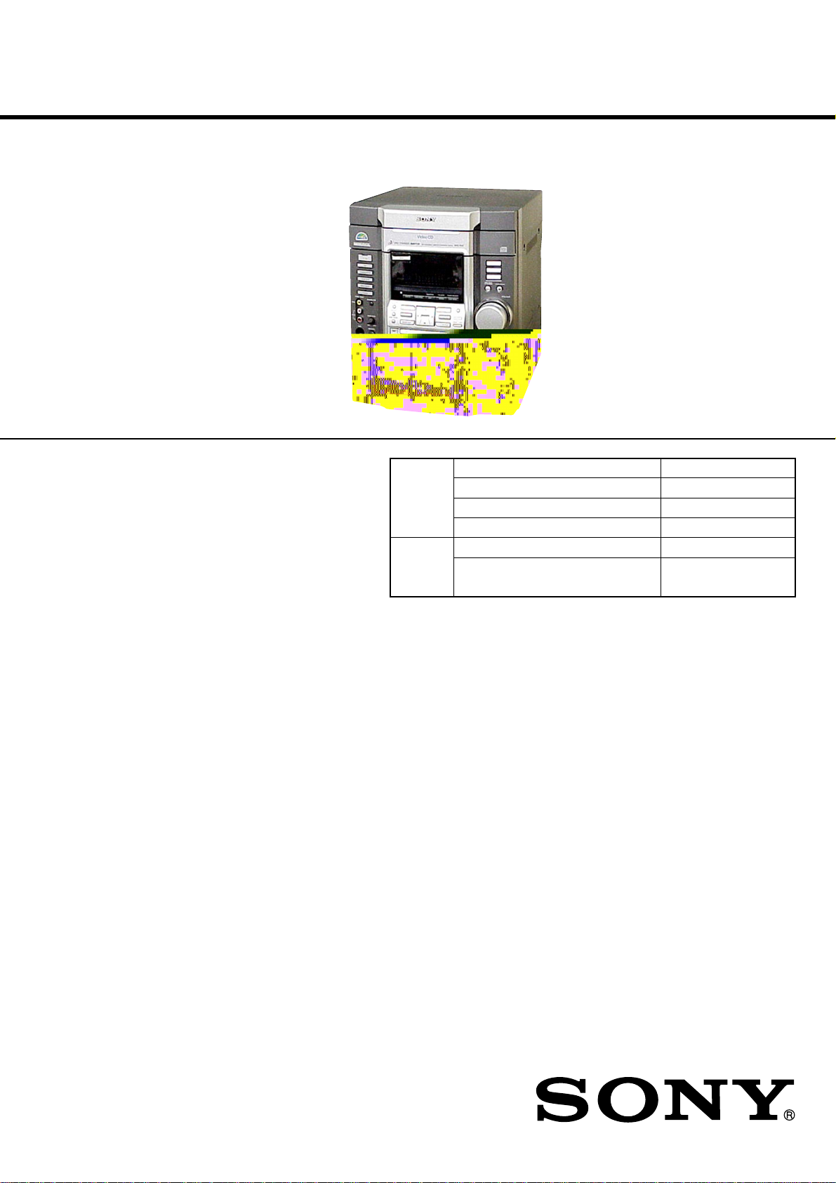
• HCD-RV2/RV5/RV6 is the tuner,
deck, CD and amplifier section in
MHC-RV2/RV5/RV6.
CD CD Mechanism Type CDM58E-30BD62
Section Base Unit Name BU-30BD62
Tape Deck
Section Tape Transport Mechanism Type
E Model
HCD-RV2/RV5/RV6
Tourist Model
HCD-RV5
Model Name Using Similar Mechanism NEW
Optical Pick-up Name A-MAX.3
Model Name Using Similar Machanism NEW
RV2: CWM43FF-05
RV5/RV6: CWM48RR-01
Amplifier section
HCD-RV2:
The following measured at AC 120, 127, 220, 240 V,
50/60 Hz
DIN power output (rated)
50 + 50 watts
Continuous RMS power output (reference)
60 + 60 watts (6 ohms at
1 kHz, 10% THD)
HCD-RV6:
The following measured at AC 120, 127, 220, 240 V,
50/60 Hz
DIN power output (rated)
115 + 115 watts
Continuous RMS power output (reference)
140 + 140 watts (6 ohms at
1 kHz, 10% THD)
HCD-RV5:
The following measured at AC 120, 127, 220, 240 V,
50/60 Hz
DIN power output (rated)
100 + 100 watts
Continuous RMS power output (reference)
120 + 120 watts (6 ohms at
1 kHz, 10% THD)
SPECIFICATIONS
Inputs
HCD-RV2:
GAME INPUT (VIDEO) (phono jack):
1 Vp-p, 75 ohms
GAME INPUT (AUDIO) (phono jacks):
voltage 450 mV,
impedance 47 kilohms
MIC (phone jack): sensitivity 1 mV,
impedance 10 kilohms
Outputs
VIDEO OUT (phono jack):
max. output level
1 Vp-p, unbalanced, Sync
negative, load impedance
75 ohms
PHONES (stereo mini jack):
accepts headphones of
8 ohms or more
SPEAKER: accepts impedance of 6 to
16 ohms
– Continued on next page –
COMPACT DISC DECK RECEIVER
9-874-131-03
2002K0400-1
© 2002. 11
Sony Corporation
Home Audio Company
Published by Sony Engineering Corporation
1
Page 2

HCD-RV2/RV5/RV6
HCD-RV5/RV6:
MD/VIDEO (AUDIO) IN (phono jacks):
voltage 450/250 mV,
impedance 47 kilohms
GAME INPUT (VIDEO) (phono jack):
1 Vp-p, 75 ohms
GAME INPUT (AUDIO) (phono jack):
voltage 450 mV,
impedance 47 kilohms
MIC (phone jack): sensitivity 1 mV,
impedance 10 kilohms
Outputs
PHONES (stereo mini jack):
accepts headphones of
8 ohms or more
SPEAKER: accepts impedance of 6 to
16 ohms
SURROUND SPEAKER (HCD-RV6 only)
accepts impedance of 24
ohms
MD/VIDEO (AUDIO) OUT (phono jacks):
impedance 1 kilohms
VIDEO OUT (phono jack):
1 Vp-p,
impedance 75 ohms
Disc player section
System Compact disc and digital
audio and video system
Laser Semiconductor laser
(λ=780 nm)
Emission duration:
continuous
Frequency response 2 Hz – 20 kHz (±0.5 dB)
Wavelength 780 – 790 nm
Signal-to-noise ratio More than 90 dB
Dynamic range More than 90 dB
Video color system format
NTSC, PAL
Tape deck section
Recording system 4-track 2-channel stereo
Frequency response 40 – 13,000 Hz (±3 dB),
using Sony TYPE I
cassette
Wow and flutter ±0.15% W.Peak (IEC)
0.1% W.RMS (NAB)
±0.2% W.Peak (DIN)
Tuner section
FM stereo, FM/AM superheterodyne tuner
FM tuner section
Tuning range 87.5 – 108.0 MHz
Antenna FM lead antenna
Antenna terminals 75 ohm unbalanced
Intermediate frequency 10.7 MHz
AM tuner section
Tuning range
Middle Eastern and Philippine models:
531 – 1,602 kHz (with the
interval set at 9 kHz)
Other models: 531 – 1,602 kHz (with the
interval set at 9 kHz)
530 – 1,710 kHz (with the
interval set at 10 kHz)
Antenna AM loop antenna
Antenna terminals External antenna terminal
Intermediate frequency 450 kHz
Front speaker SS-RV900 for HCD-RV6/RV5:
Speaker system 3-way, 3-unit, bass-reflex
type
Speaker units
Sub Woofer: 13 cm, cone type
Woofer: 13 cm, cone type
Tweeter: 5 cm, cone type
Nominal impedance 6 ohms
Dimensions (w/h/d) Approx. 215 × 356 × 285 mm
Mass Approx. 4.5 kg net per
speaker
Surround speaker SS-RSV6 for HCD-RV6:
Speaker system 2-way, 2-unit, bass-reflex
type
Speaker units
Woofer: 10 cm, cone type
Tweeter: 5 cm, cone type
Nominal impedance 24 ohms
Dimensions (w/h/d) Approx. 150 × 325 × 220 mm
Mass Approx. 2.3 kg net per
speaker
General
Power requirements
Saudi Arabian model: 120 – 127 V, 220 V or
230 – 240 V AC,
50/60 Hz
Adjustable with voltage
selector
Thai model: 220 V AC, 50/60 Hz
Other models: 120 V, 220 V or 230 –
240 V AC, 50/60 Hz
Adjustable with voltage
selector
Power consumption
HCD-RV2: 115 watts
HCD-RV5: 200 watts
HCD-RV6: 220 watts
Dimensions (w/h/d)
HCD-RV2: Approx. 280 × 325 × 412 mm
HCD-RV5/RV6: Approx. 280 × 325 × 421 mm
Mass
HCD-RV2: Approx. 9.0 kg
HCD-RV5: Approx. 10.0 kg
HCD-RV6: Approx. 10.5 kg
Supplied accessories: AM loop antenna (1)
Remote Commander (1)
Batteries (2)
FM lead antenna (1)
Speaker pads (8)
Video cable (1)
Design and specifications are subject to change without
notice.
Speaker
HCD-RV2:
Speaker system 3-way, 3-unit,
bass-reflex type
Speaker units
Woofer: 13 cm, cone type
Tweeter: 5 cm, cone type
Super Tweeter: 2 cm, dome type
Nominal impedance 6 ohms
Dimensions (w/h/d) Approx. 200 × 325 × 237 mm
Mass Approx. 3.6 kg net per
speaker
2
SAFETY-RELATED COMPONENT WARNING!!
COMPONENTS IDENTIFIED BY MARK 0 OR DOTTED LINE
WITH MARK 0 ON THE SCHEMATIC DIAGRAMS AND IN
THE PARTS LIST ARE CRITICAL TO SAFE OPERATION.
REPLACE THESE COMPONENTS WITH SONY P ARTS WHOSE
PART NUMBERS APPEAR AS SHOWN IN THIS MANUAL OR
IN SUPPLEMENTS PUBLISHED BY SONY.
Page 3
HCD-RV2/RV5/RV6
CAUTION
Use of controls or adjustments or performance of procedures
other than those specified herein may result in hazardous
radiation exposure.
Notes on Chip Component Replacement
• Never reuse a disconnected chip component.
• Notice that the minus side of a tantalum capacitor may be
damaged by heat.
Flexible Circuit Board Repairing
• Keep the temperature of soldering iron around 270°C during
repairing.
• Do not touch the soldering iron on the same conductor of the
circuit board (within 3 times).
• Be careful not to apply force on the conductor when soldering
or unsoldering.
NOTES ON HANDLING THE OPTICAL PICK-UP BLOCK
OR BASE UNIT
The laser diode in the optical pick-up block may suffer electrostatic
breakdown because of the potential difference generated by the
charged electrostatic load, etc. on clothing and the human body.
During repair, pay attention to electrostatic break-down and also
use the procedure in the printed matter which is included in the
repair parts.
The flexible board is easily damaged and should be handled with
care.
NOTES ON LASER DIODE EMISSION CHECK
The laser beam on this model is concentrated so as to be focused on
the disc reflective surface by the objective lens in the optical pickup block. Therefore, when checking the laser diode emission,
observe from more than 30 cm away from the objective lens.
MODEL IDENTIFICATION
– BACK PANEL –
PARTS No.
MODEL PARTS No.
RV2: E3, EA, MY, SP 4-238-649-6s
RV2: TH 4-238-649-7s
RV5: E3, EA, MY, JE, SP 4-238-649-8s
RV5: TH 4-238-649-9s
RV6: E3, EA, MY, SP 4-239-344-0s
RV6: TH 4-239-344-1s
• Abbreviation
E3 : 240 V AC area in E model
EA : Saudi Arabia model
MY : Malaysia model
SP : Singapore model
TH : Thai model
JE : T ourist model
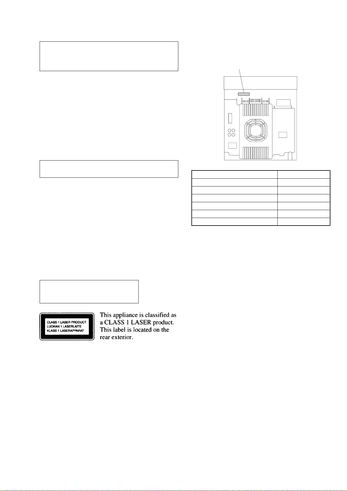
Laser component in this product is capable
of emitting radiation exceeding the limit for
Class 1.
SETTING AND RELEASING THE CD DISC TRAY LOCK
FUNCTION
This set has a disc tray lock function to prevent discs for
demonstration at shops from theft. While this lock function is set,
the tray will not be delivered out even when the OPEN/CLOSE
button is pressed.
Setting method:
Press the OPEN/CLOSE button while pressing the STOP button.
After a few seconds, the message “LOCKED” will appear on the
fluorescent indicator tube with the tray locked.
Releasing method:
Just as the lock is set, press the OPEN/CLOSE button while
pressing the STOP button.
After a few seconds, the message “UNLOCKED” will appear with
the lock released.
3
Page 4

HCD-RV2/RV5/RV6
TABLE OF CONTENTS
1. SERVICE NOTE ................................................................ 5
2. GENERAL
Main Unit (HCD-RV2) ............................................................ 6
Remote Control (HCD-RV2) ................................................... 6
Main Unit (HCD-RV5/RV6) ................................................... 7
Remote Control (HCD-RV5/RV6) .......................................... 7
3. DISASSEMBLY
3-1. Case (Top) ........................................................................... 9
3-2. Video Board.........................................................................9
3-3. CD (Door) ......................................................................... 10
3-4. Front Panel Section ........................................................... 11
3-5. Tape Mechanism Deck ...................................................... 12
3-6. Panel Board ....................................................................... 12
3-7. Key Board ......................................................................... 13
3-8. Sensor Board, DC Fan (FAN961) ..................................... 13
3-9. Main Board, Power Amp Board ........................................ 14
3-10. Base Unit ...........................................................................14
3-11. Driver Board, Motor Board, Sensor (CD) Board ..............15
4. DIAGRAMS
4-1. Circuit Boards Location .................................................... 16
4-2. Printed Wiring Board –BD Section–.................................18
4-3. Schematic Diagram –BD Section–.................................... 19
4-4. Printed Wiring Boards –CD Section– ............................... 20
4-5. Schematic Diagram –CD Section–.................................... 21
4-6. Printed Wiring Board –Video Section–.............................22
4-7. Schematic Diagram –Video Section (1/2)–....................... 24
4-8. Schematic Diagram –Video Section (2/2)–....................... 25
4-9. Schematic Diagram –Main Section (1/4)– ........................26
4-10. Schematic Diagram –Main Section (2/4)– ........................27
4-11. Schematic Diagram –Main Section (3/4)– ........................28
4-12. Schematic Diagram –Main Section (4/4)– ........................29
4-13. Printed Wiring Boards –Main Section– ............................ 30
4-14. Printed Wiring Boards –Panel Section (HCD-RV2)– ....... 31
4-15. Printed Wiring Board –Key Section (HCD-RV2)– ........... 32
4-16. Schematic Diagram –Panel Section (HCD-RV2)–............33
4-17. Printed Wiring Boards –Panel Section (HCD-RV5)– ....... 34
4-18. Printed Wiring Board –Key Section (HCD-RV5)– ........... 35
4-19. Schematic Diagram –Panel Section (HCD-RV5)–............36
4-20. Printed Wiring Boards –Panel Section (HCD-RV6)– ....... 37
4-21. Printed Wiring Board –Key Section (HCD-RV6)– ........... 38
4-22. Schematic Diagram –Panel Section (HCD-RV6)–............39
4-23. Printed Wiring Board
–Power Amp Section (HCD-RV2)– .................................. 40
4-24. Printed Wiring Board –Trans Section (HCD-RV2)–.........41
4-25. Printed Wiring Board
–Sub Trans Section (HCD-RV2)– ..................................... 42
4-26. Schematic Diagram –Power Section (HCD-RV2)– .......... 43
4-27. Printed Wiring Boards
–Power Amp Section (HCD-RV5)– .................................. 44
4-28. Printed Wiring Board –Trans Section (HCD-RV5)–.........45
4-29. Printed Wiring Board
–Sub Trans Section (HCD-RV5)– ..................................... 46
4-30. Schematic Diagram –Power Section (HCD-RV5)– .......... 47
4-31. Printed Wiring Boards
–Power Amp Section (HCD-RV6)– .................................. 48
4-32. Printed Wiring Board –Trans Section (HCD-RV6)–.........49
4-33. Printed Wiring Board
–Sub Trans Section (HCD-RV6)– ..................................... 50
4-34. Schematic Diagram –Power Section (HCD-RV6)– .......... 51
4-35. IC Block Diagrams............................................................ 52
5. EXPLODED VIEWS
5-1. Main Section ..................................................................... 56
5-2. Front Panel Section ........................................................... 57
5-3. Main Board Section .......................................................... 58
5-4. CD Mechanism Deck Section ........................................... 59
5-5. Optical Pick-up Section..................................................... 60
6. ELECTRICAL PARTS LIST ........................................ 61
4
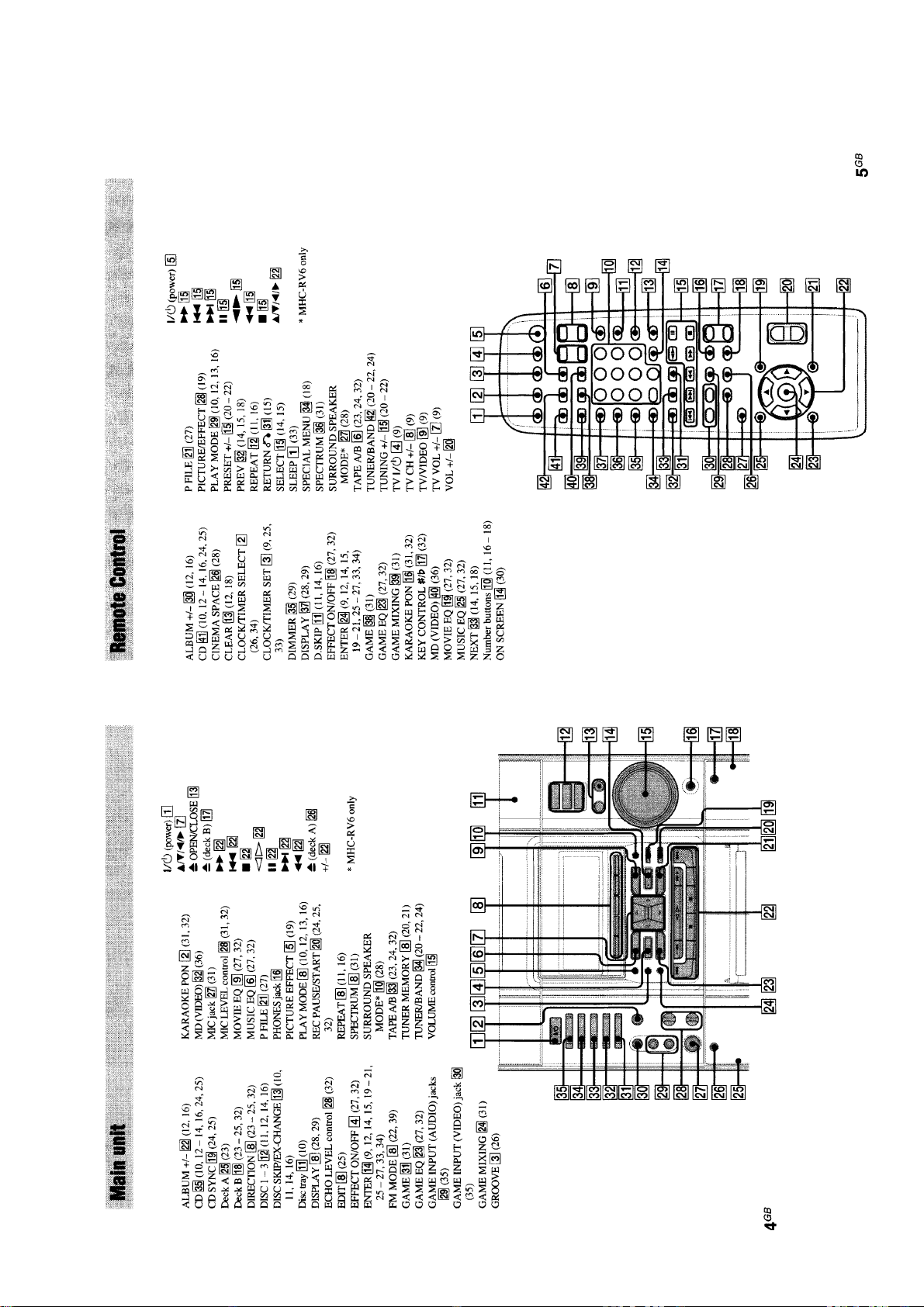
Page 5
SECTION 1
d
SERVICE NOTE
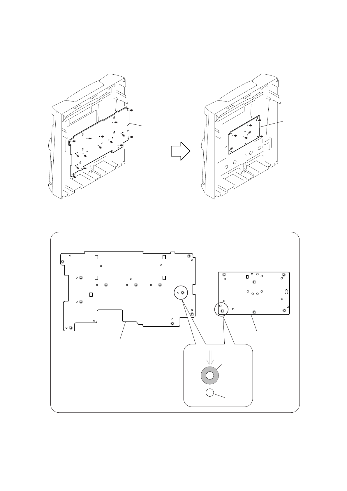
REMOVING THE PANEL BOARD AND THE KEY BOARD
* The panel board and the key board only are connected to the front panel
by means of hot-melting the plastics.
2
PANEL board
HCD-RV2/RV5/RV6
4
KEY boar
1
Cut the fifteen melted-connection points
with a cutting plier.
Note for installing the panel board and the key board
PANEL board
(eleven screw holes)
3
Cut the seven melted-connection points
with a cutting plier.
KEY board
(six screw holes)
Screw hole
In order to re-install the panel board and the key board,
fix them by using the screws (+BVTP 2.6
Screw in to the respective screw holes.
Do not tighten the screws excessively.
×
8 ) respectively.
Hot melt
5
Page 6
HCD-RV2/RV5/RV6
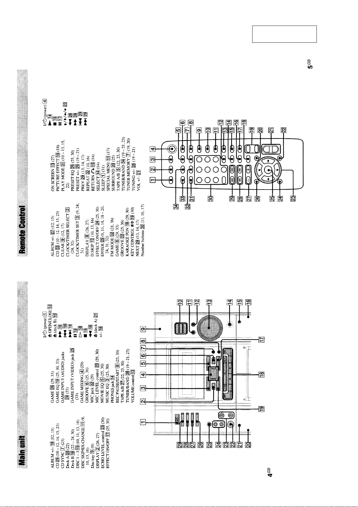
SECTION 2
GENERAL
This section is extracted
from instruction manual.
(HCD-RV2)
(HCD-RV2)
6
Page 7
HCD-RV2/RV5/RV6
(HCD-RV5/RV6)
(HCD-RV5/RV6)
7
Page 8
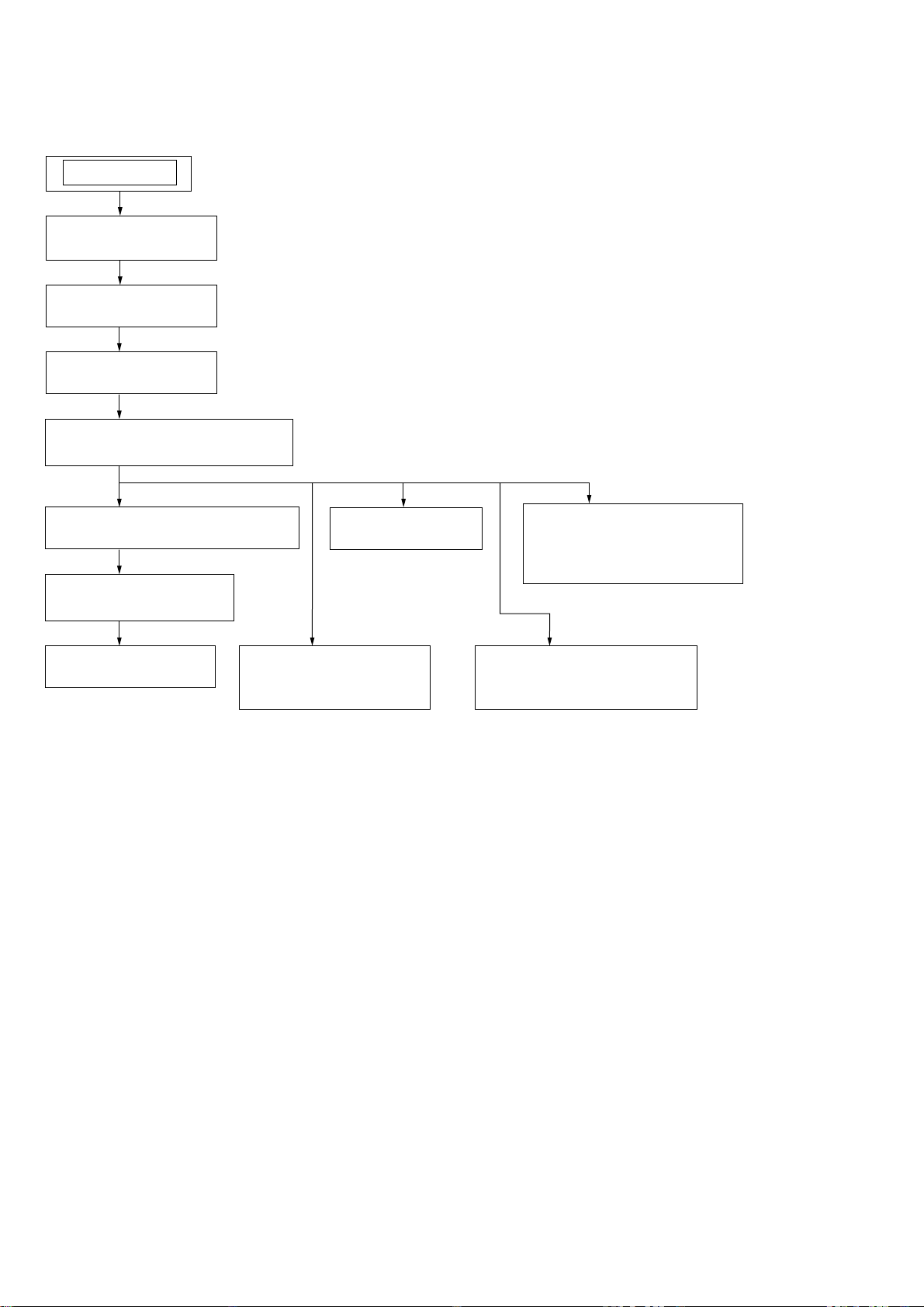
HCD-RV2/RV5/RV6
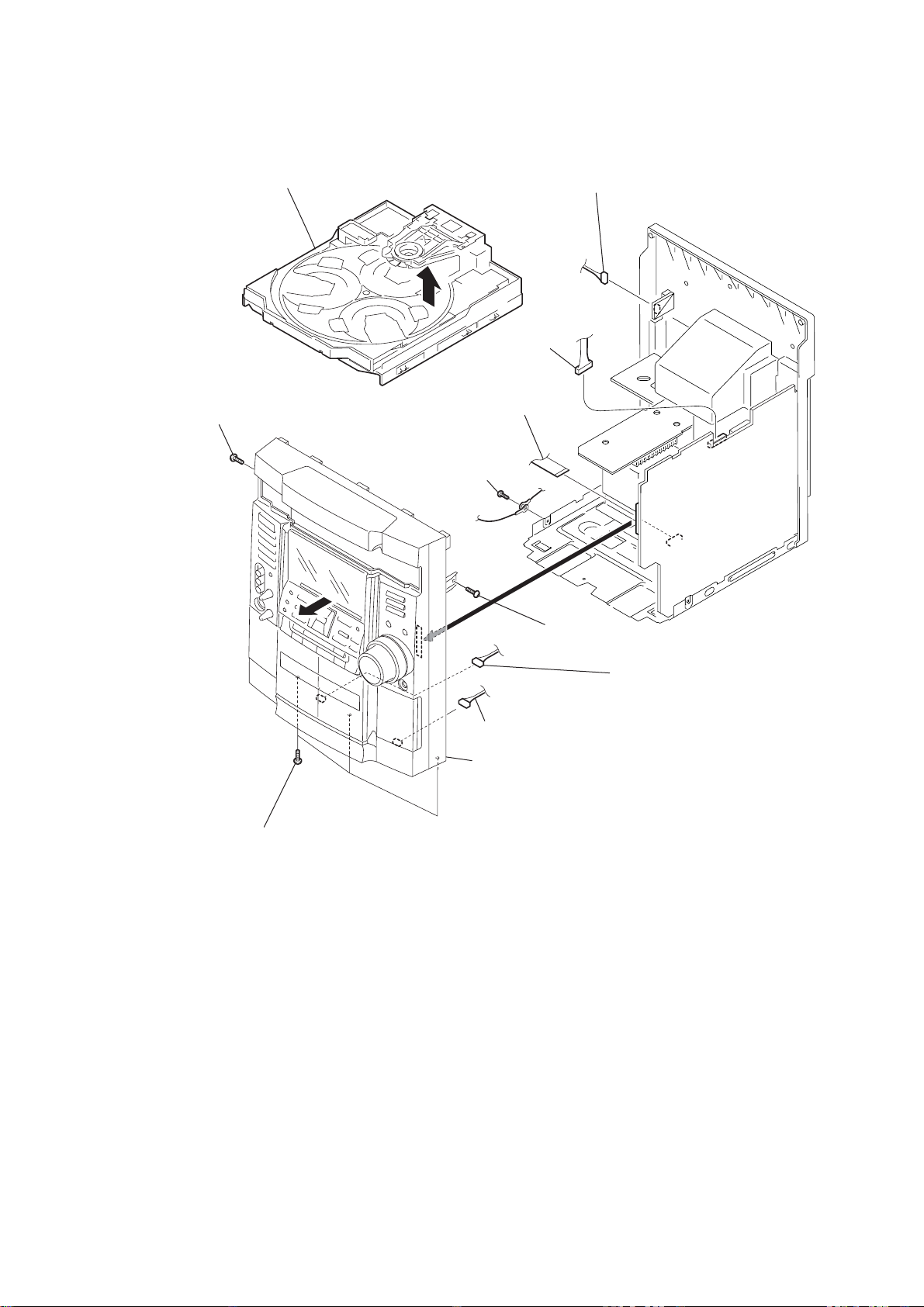
Note : Disassemble the unit in the order as shown below.
SET
3-1. CASE (TOP)
(Page 9)
3-2. VIDEO BOARD
(Page 9)
3-3. CD (DOOR)
(Page 10)
3-4. FRONT PANEL SECTION
(Page 11)
SECTION 3
DISASSEMBLY
3-5. TAPE MECHANISM DECK
(Page 12)
3-6. PANEL BOARD
(Page 12)
3-7. KEY BOARD
(Page 13)
3-8. SENSOR BOARD
3-10. BASE UNIT
(Page 14)
DC FAN (FAN961)
(Page 13)
3-11. DRIVER BOARD,
MOTOR BOARD,
SENSOR (CD) BOARD
(Page 15)
3-9. MAIN BOARD,
POWER AMP BOARD
(Page 14)
8
Page 9
Note : Follow the disassembly procedure in the numerical order given.
)
HCD-RV2/RV5/RV6
3-1. CASE (TOP)
two screws (case 3 TP2)
7
8
screw (case 3 TP2)
qs
0
screw
(+BVTT 3
qg
case (side-L)
9
(+BVTP 3
×
8)
case (top)
screw
qd
four screws (+BVTP 3
qf
×
10)
qa
5
×
10)
6
case (side-R)
1
(case 3 TP2)
3
screw
(+BVTP 3
two screws
×
10
3-2. VIDEO BOARD
5
VIDEO board
2
3
CN101
CN201
(flat type)
(flat type)
4
(+BVTT 3
2
screw (case 3 TP2)
screw
×
8)
1
CN301
4
two screws (+BVTP 3
×
10)
9
Page 10
HCD-RV2/RV5/RV6
3-3. CD (DOOR)
CD mechanism deck (CDM58F)
1
Turn the pulley to the direction of arrow.
Front panel side
4
CD door
pulley
2
Pull-out the disc tray.
3
10
Page 11
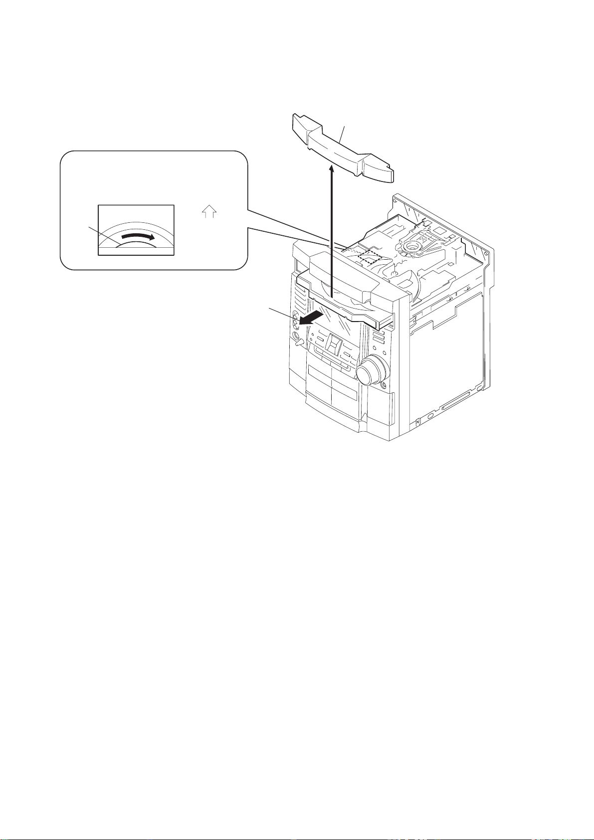
3-4. FRONT PANEL SECTION
qf
CD mechanism deck (CDM58E)
6
screw
(+BVTP 3
×
10)
qs
5
screw
(+BVTP 3
2
×
10)
qd
CN103
CN671
(flat type)
1
HCD-RV2/RV5/RV6
CN685
9
8
three screws (+BVTP 3
×6
0
3
qa
front panel section
)
7
(+BVTP 3
connector 6p
screw
×
10)
4
connector 3p
11
Page 12
HCD-RV2/RV5/RV6
)
3-5. TAPE MECHANISM DECK
2
tape mechanism deck
1
six
screws
(+BVTP 2.6
×
8
3-6. PANEL BOARD
claws
2
CN704
6
PANEL board
7
CN712
claws
3
three
(+BVTP 2.6
screws
×
8)
4
(+BVTP 2.6
5
(+BVTP 2.6
six
two
screws
screws
×
8)
×
8)
12
1
volume knob
Page 13
3-7. KEY BOARD
claw
3
two
screws
(+BVTP 2.6
2
(+BVTP 2.6
4
KEY board
×
8)
two
screws
1
two
screws
(+BVTP 2.6
HCD-RV2/RV5/RV6
×
8)
×
8)
3-8. SENSOR BOARD, DC FAN (FAN961)
8
cover (duct)
0
SENSOR board
9
screw
(+BVTP 2.6
×
4
8)
CN504
1
CN901
3
CN903
5
2
CN304
CN2
qd
6
CN305
7
two screws
(+BVTP 3
qs
(+BVTP 3
qf
×
10)
six screws
qg
(+BVTP 3
qa
(+BVTT 3
panel back
two screws
two screws
×
10)
×
16)
×
6)
qh
DC fan (FAN961)
13
Page 14
HCD-RV2/RV5/RV6
3-9. MAIN BOARD, POWER AMP BOARD
4
three
(+BVTP 3
6
POWER AMP board
5
two
screws
×
(+BVTP 3
16)
1
CN915
screws
×
10)
MAIN board
3
MAIN board
3-10. BASE UNIT
8
two insulators
6
two
coil springs (insulator)
5
two stoppers (BU)
7
base unit
9
two insulators
3
two
coil springs (insulator)
2
two
screws (+PTPWH M2.6)
2
two
screws
(+BVTP 3
×
10)
14
4
two screws (+BVTP 2.6
1
×
8)
screw (DIA. 12)
Page 15
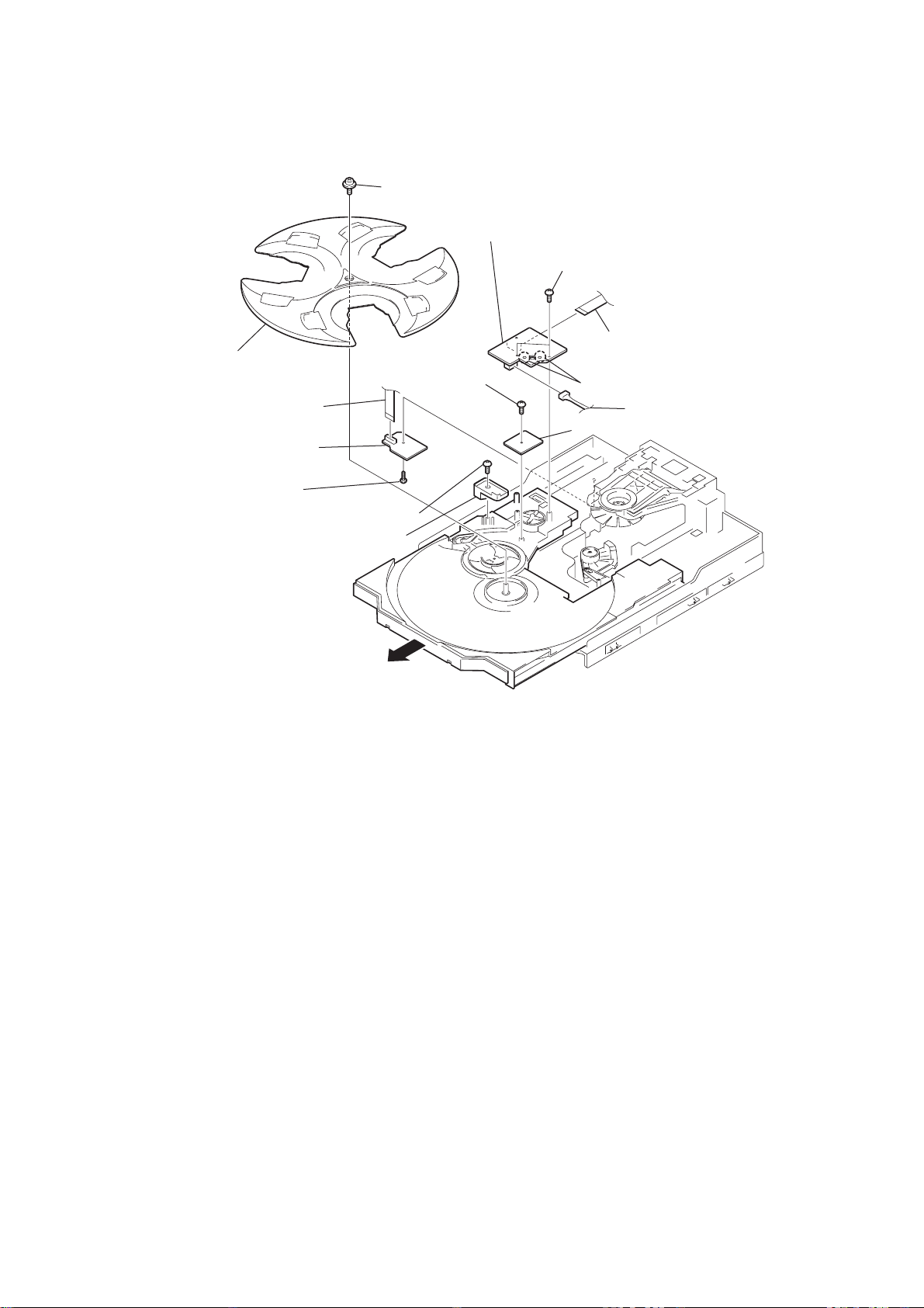
3-11. DRIVER BOARD, MOTOR BOARD, SENSOR (CD) BOARD
qs
qd
tray
3
CN702 (flat type)
2
DRIVER board
1
screw
(+BVTP 2.6
×
8)
4
screw (+BVTP 2.6
5
stopper (tray)
screw (+PTPWH 2.6
0
qf
screw
(+BVTP 2.6
×
8)
×
8)
MOTOR board
×
8)
HCD-RV2/RV5/RV6
6
two screws (+BVTP 2.6
8
CN721(flat type)
7
Remove the two solderings of motor.
9
CN722
qg
SENSOR (CD) board
×
8)
qa
Pull-out the disc tray.
15
Page 16
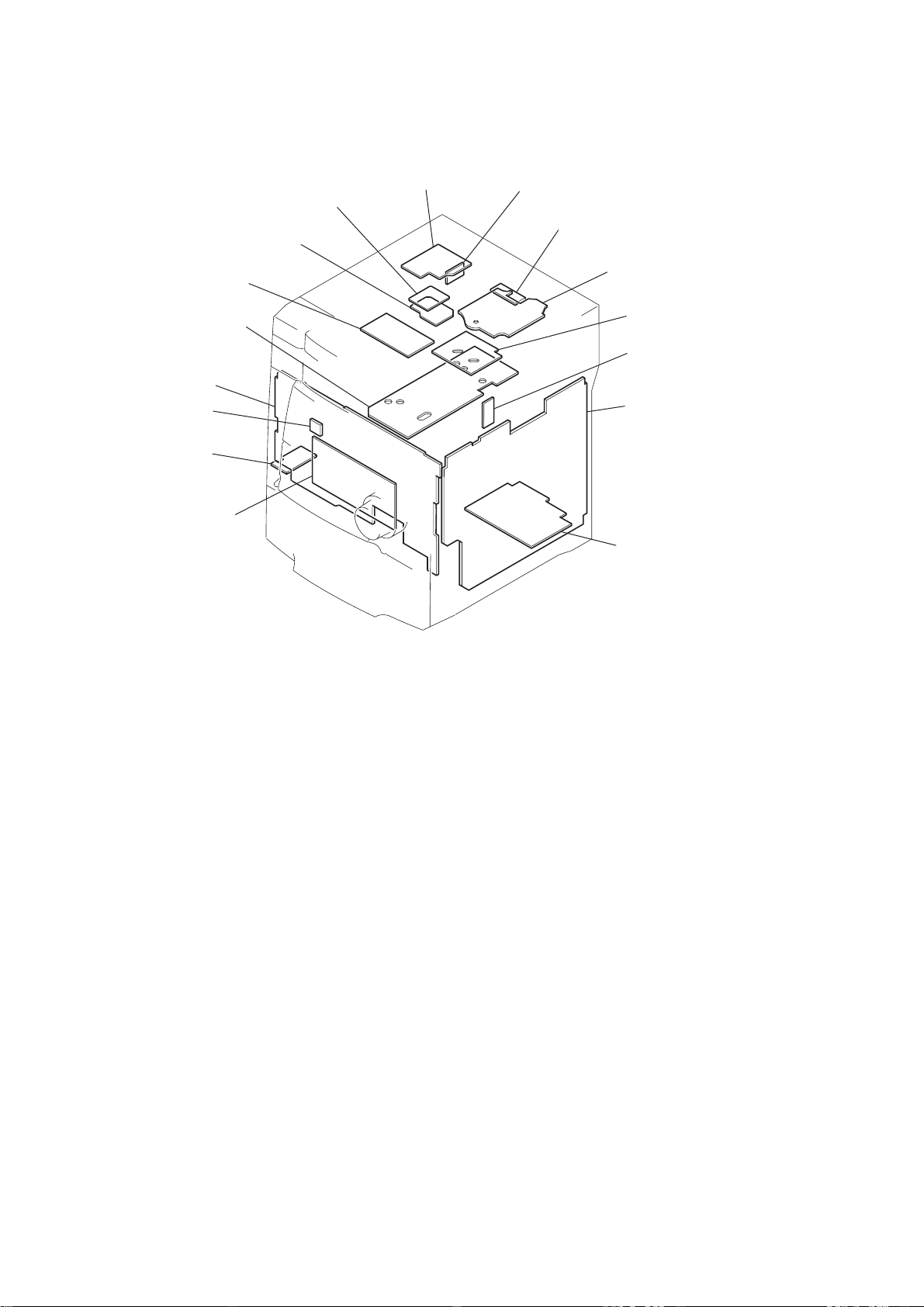
HCD-RV2/RV5/RV6
)
4-1. CIRCUIT BOARDS LOCATION
SECTION 4
DIAGRAMS
VIDEO board
TRANS board
PANEL board
REMOTE board
MIC board
KEY board
SENSOR (CD) board
DRIVER board
MOTOR board
VIDEO OUT board
SENSOR board
(HCD-RV5/RV6)
BD board
SUB TRANS board
SURROUND board
(HCD-RV6
MAIN board
POWER AMP board
16
Page 17
HCD-RV2/RV5/RV6
THIS NOTE IS COMMON FOR PRINTED WIRING
BOARDS AND SCHEMATIC DIAGRAMS.
(In addition to this, the necessary note is
printed in each block.)
for schematic diagram:
• All capacitors are in µF unless otherwise noted. pF: µµF
50 WV or less are not indicated except for electrolytics
and tantalums.
• All resistors are in Ω and 1/
specified.
•%: indicates tolerance.
f
•
• C : panel designation.
Note: The components identified by mark 0 or dotted line
• A : B+ Line.
• B : B– Line.
• H : adjustment for repair.
•Voltage and waveforms are dc with respect to ground
•Voltages are taken with a VOM (Input impedance 10 MΩ).
• BD section
• VIDEO (1/2), (2/2), MAIN (1/4), (2/4), (3/4), (4/4), P ANEL,
•Waveforms are taken with a oscilloscope.
• Circled numbers refer to waveforms.
• Signal path.
• Abbreviation
: internal component.
with mark 0 are critical for safety.
Replace only with part number specified.
under no-signal (detuned) conditions.
Voltage variations may be noted due to normal produc-
tion tolerances.
no mark : CD
POWER sections.
no mark : FM
(): CD
[]: TAPE
Voltage variations may be noted due to normal production tolerances.
F : FM
f : AM
E : PB (DECK A)
d : PB (DECK B)
G : REC (DECK B)
J : CD
L : VIDEO
E3 : 240 V AC area in E model
EA : Saudi Arabia model
MY : Malaysia model
SP : Singapore model
TH : Thai model
4
W or less unless otherwise
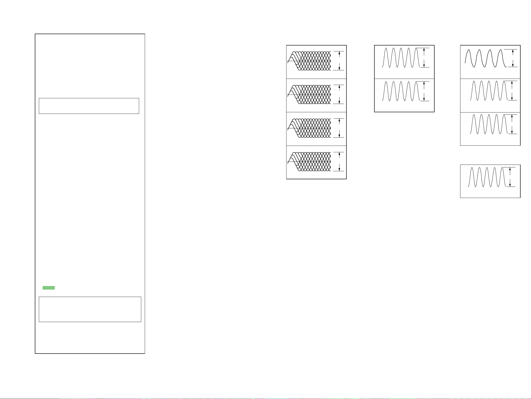
•Waveforms
– BD Board –
1
IC103
6
2
IC103
7
3
IC103
qg
4
IC103
wk
Approx.
160mVp-p
(A), 8 (C)
Approx.
160mVp-p
(B), 9 (D)
Approx.
1Vp-p
(RFAC)
Approx.
0.6Vp-p
(RFDCO)
– VIDEO Board –
1
33.8688MHz
IC505
(XTAO)
<zb/>
2
29MHz
IC505
(CLKA)
<x/n>
1.1Vp-p
0.6Vp-p
– MAIN Board –
1
4.5MHz
1
(XIN)
IC102
2
32.768kHz
IC601
(XCOUT)
qa
3
16MHz
IC601
(XOUT)
qd
– PANEL Board –
1
5MHz
IC701
3
1.8Vp-p
2.8Vp-p
0.6Vp-p
3Vp-p
(X1)
for printed wiring boards:
• X : parts extracted from the component side.
• Y : parts extracted from the conductor side.
• x : parts mounted on the conductor side.
• : Pattern from the side which enables seeing.
(The other layer’s patterns are not indicated.)
Caution:
Pattern face side: Parts on the pattern face side seen from the
(Side B) pattern face are indicated.
Parts face side: Parts on the parts face side seen from the
(Side A) parts face are indicated.
• Abbreviation
E3 : 240 V AC area in E model
EA : Saudi Arabia model
MY : Malaysia model
SP : Singapore model
TH : Thai model
17 17
Page 18
HCD-RV2/RV5/RV6
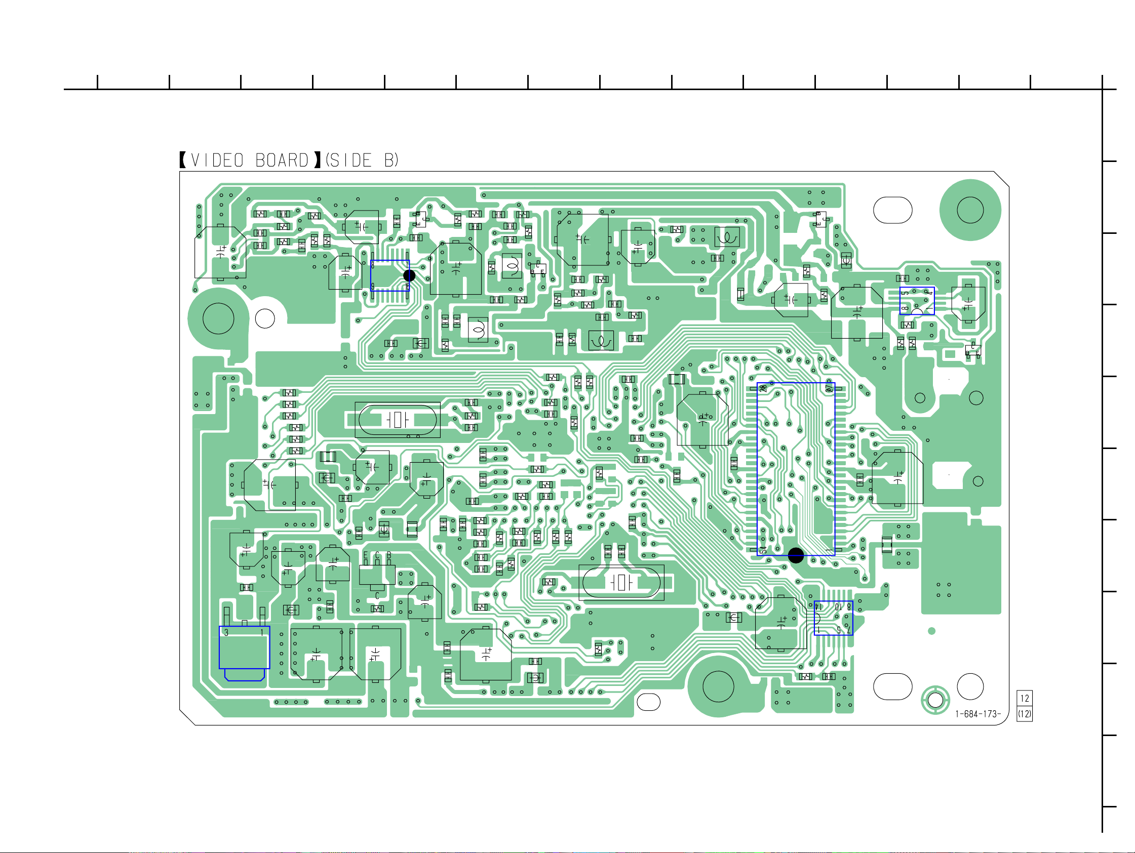
4-2. PRINTED WIRING BOARD — BD SECTION — • Refer to page 16 for Circuit Boards Location.
A
B
C
D
E
F
1
234567891011 12 13 14
M101
C163
C182
C166
C164
C165
C153
R228
C101
R227
R126
C102
R229
C104
C109
C112
C103
R117
C120
C111
C115
C108
C117
R113
R109
R102
R105
R111
Q102
C110
R103
R118
R114
R179
R176
R104
C107
R120
R112
IC103
C213
R226
R152
C151
R235
IC102
R151
R236
R231
CN101
(Page 22)
G
H
R125
C114
I
• Semiconductor
C119
C113
R122
R123
Q101
R124
R234
C118
CN102
M102
Location
Ref. No. Location
IC102 C-12
IC103 F-9
Q101 G-9
Q102 C-9
1818
Page 19
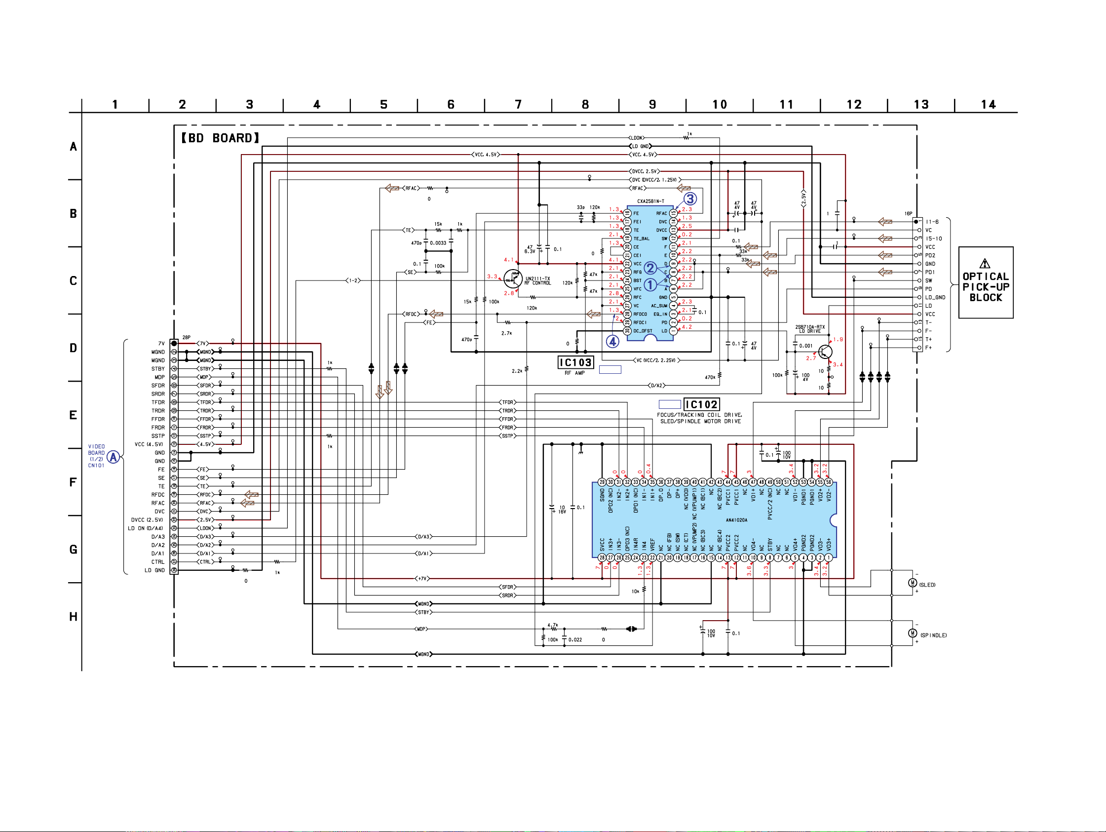
• Refer to page 17 for Waveforms.
4-3. SCHEMATIC DIAGRAM — BD SECTION — • Refer to page 52 for IC Block Diagrams.
TP49
C213
R105
R102
C104C101
C102
R103
R104
C103
(Page 24)
CN101
TP56
TP57
TP58
TP59
TP60
TP61
TP62
TP63
TP64
TP65
TP66
TP67
TP69
TP70
TP71
TP72
TP73
TP74
TP75
TP76
TP77
TP78
TP79
TP80
TP55
TP68
R234
R226
R236
R235
TP17
TP18
TP21
TP19
R227
R113
R229
C115
R109
Q102
C117
C165
R111
R118
TP27
C107
C153
R120
R112
R114
R117
IC B/D
R179
IC103
R231
IC B/D
TP24
C110
R228
R126
R125
C112
C109
TP23
C108
IC102
C120
C111
C166
R122
C182
C114
C113
Q101
R124
R123
C118
C119
TP22
TP26
TP25
TP54
TP16
TP53
TP52
TP15
TP14
HCD-RV2/RV5/RV6
CN102
TP51
TP50
TP13
M102
R152
R151
C151
R176
19 19
TP100
C163
C164
M101
Page 20
HCD-RV2/RV5/RV6
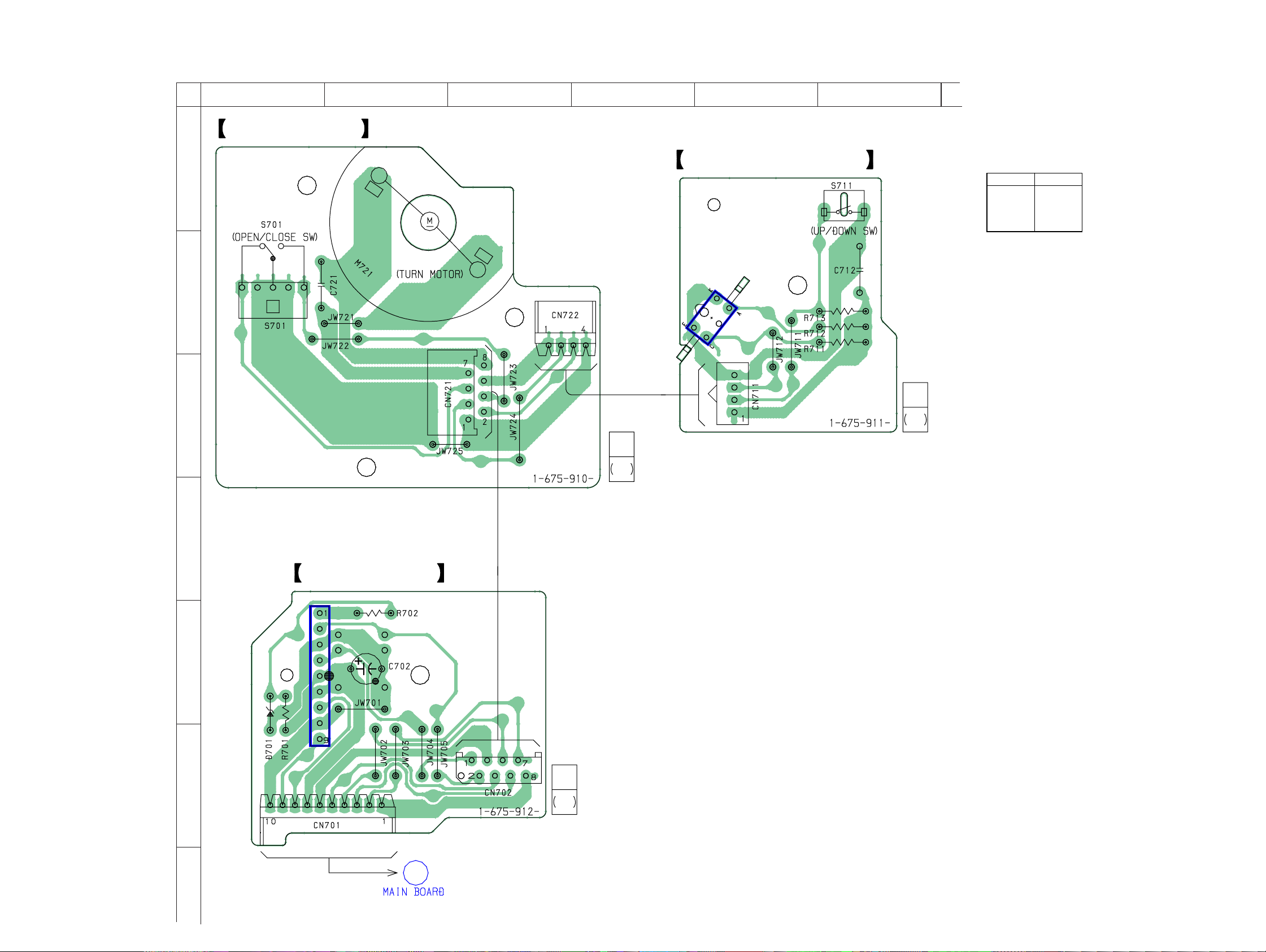
4-4. PRINTED WIRING BOARDS — CD SECTION — • Refer to page 16 for Circuit Boards Location.
A
B
C
12
MOTOR BOARD
3456
SENSOR (CD) BOARD
IC711
4
14
14
• Semiconductor
Location
Ref. No. Location
D701 F-1
IC701 E-1
IC711 B-5
D
E
14
14
DRIVER BOARD
IC701
F
G
C
CN103
14
14
(Page 30)
2020
Page 21
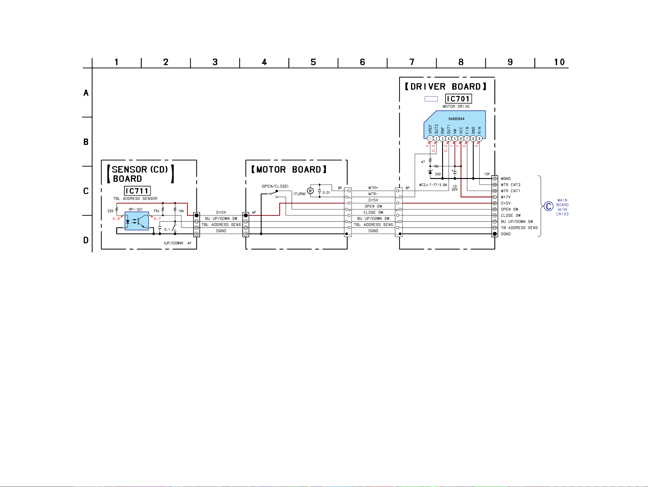
4-5. SCHEMATIC DIAGRAM — CD SECTION — • Refer to page 52 for IC Block Diagram.
HCD-RV2/RV5/RV6
IC B/D
IC701
R702
R712
IC711
R711 R713
C712
S711
CN711
CN722
S701
M721
C721
CN721
CN702
D701
R701
CN701
C702
(Page 29)
21 21
Page 22
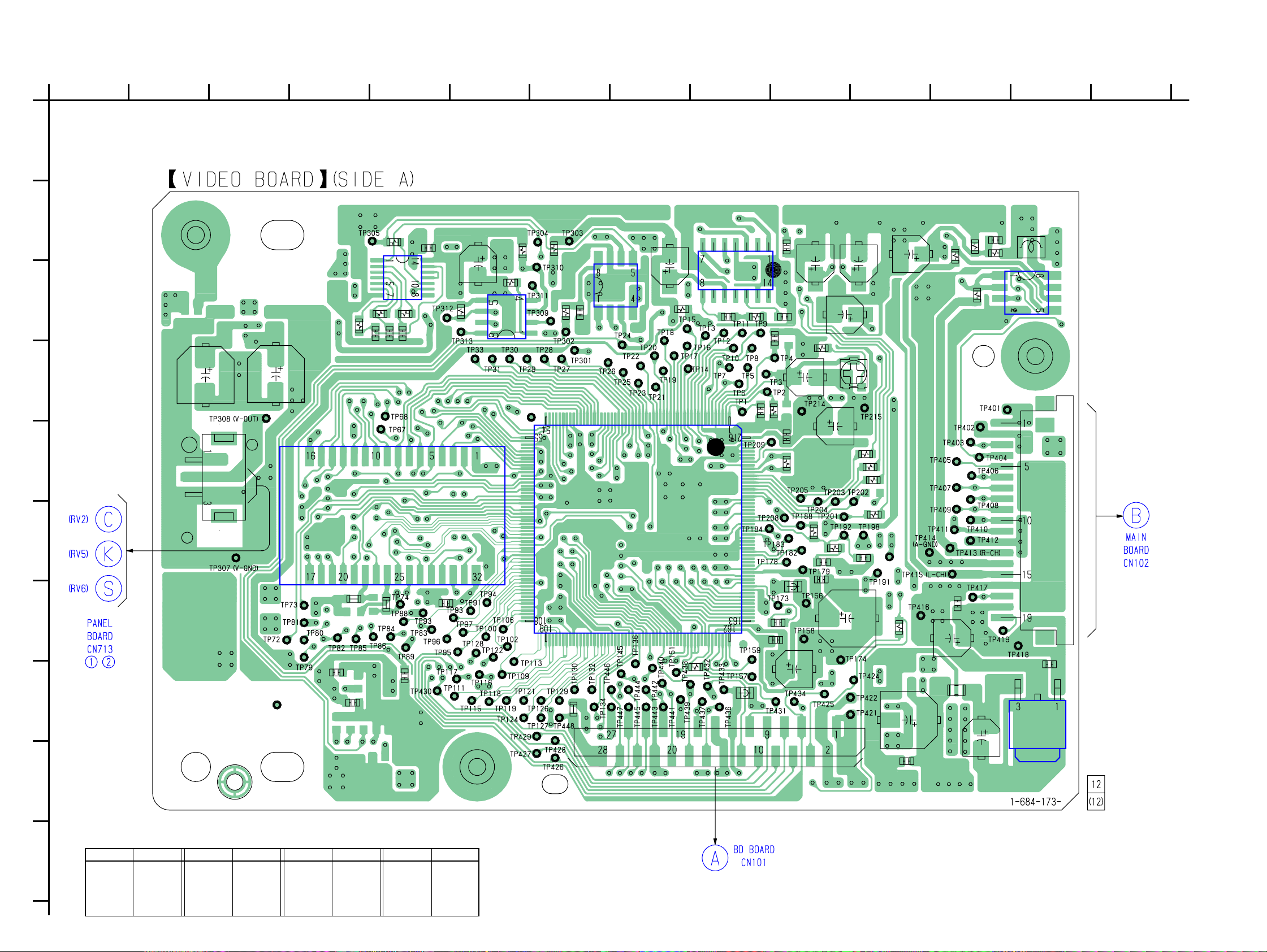
HCD-RV2/RV5/RV6
4-6. PRINTED WIRING BOARD — VIDEO SECTION — • Refer to page 16 for Circuit Boards Location.
A
B
C
D
E
F
G
1
(Page 31)
(Page 34)
(Page 37)
234567891011121314
EP200
R102
C258
C115
R115
R114
R152
L102
IC102
EP202
CN201
(Page 30)
C366
CN301
C365
JW523
R309
IC508
R310
C309
524
JW
R307R308
C308
IC302
C307
C305
C573
C301
R301
R303
IC301
R305
R302
R318
C315
IC303
IC505
C324
R323
C325
IC304
R324
C502
C326
C524
C503
R502
FB501
C570
C584
C501
C551
R558
C544
R501
R551
C582
C597
C552
R552
C540
RV501
C538
C543
C596
R557
R556
R555
R554
C114
R202
C209
H
J
C567
C561
C568
EP201
203
JW
R533
CN101
FB252
C525
FL201
C211
C214
C212
C210
IC202
I
• Semiconductor Location
Ref. No. Location
IC102 C-13
(IC201) I-13
IC202 H-13
IC301 C-6
IC302 C-5
( ) : SIDE B
Ref. No. Location Ref. No. Location Ref. No. Location
IC303 C-8
IC304 C-9
(IC307) C-3
(IC504) C-10
IC505 F-8
(IC506) H-4
(IC507) F-5
IC508 F-5
(Q201) G-11
(Q301) C-8
(Q302) B-5
(Q370) D-2
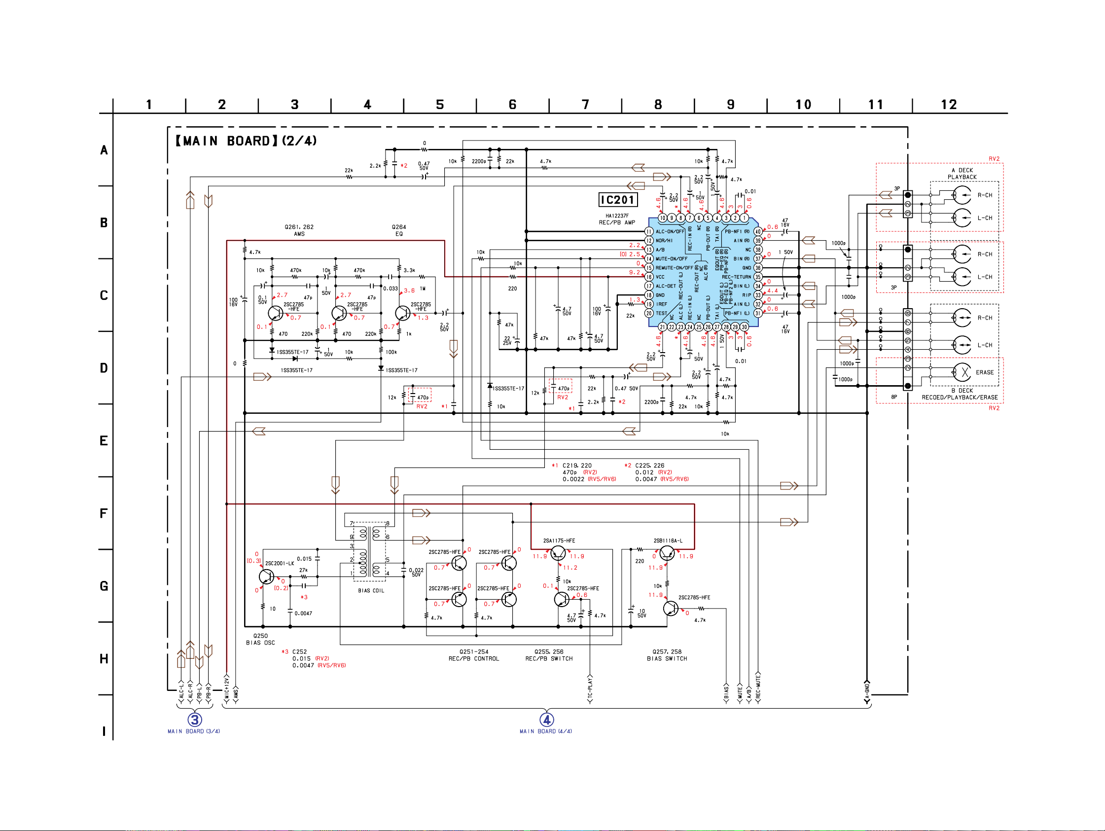
(Q581) B-10
(Page 18)
2222
Page 23
HCD-RV2/RV5/RV6
EP202
C116
C201
C202
R108
C156
C106
C259
R507
R506
R505
R504
R503
C105
R109
R159
R508
FB201
R102
C213
R107
R158
FL503
FB503
C221
R157
C205
C208
C154
C206
C547
Q201
R201
C596
IC504
C207
C581
FB502
C583
FL504
FB504
X502
Q581
C222
C321
R321
C545
C204
R581
C339
R549
C534
C537
C322
C549
C541
R582
C338
C542
R550
C539
R534
R559
C548
C327
C329
R326
C323
C546
R548
C533
L321
C328
L322
R522
R547
C536
R544
R322
R546
R327
C504
Q301
R545
R325
C535
R543
R532
R509
R513C550
R316
C311
R542
C317
R314
R511
R541
C318
R317
R311
R510
R315
C312
L311
R538
R512
C523
C505
C510
C314
R312
C313
C521
C303
C522
C513
X501
R306
FL501
C511
C575
C302
L301
C572
FB561
JW301
C566
C363
IC507
Q302
R372
R373
IC506
C360
C571
FB360
FL502
C576
C361
IC307
R376
R374
R375
Q370
C364
234567891011121314
1
A
B
C
D
E
F
G
H
IC201
C203
C257
C224
C255
C223
C254
FB251
R531
C574R561
I
J
23 23
Page 24
HCD-RV2/RV5/RV6
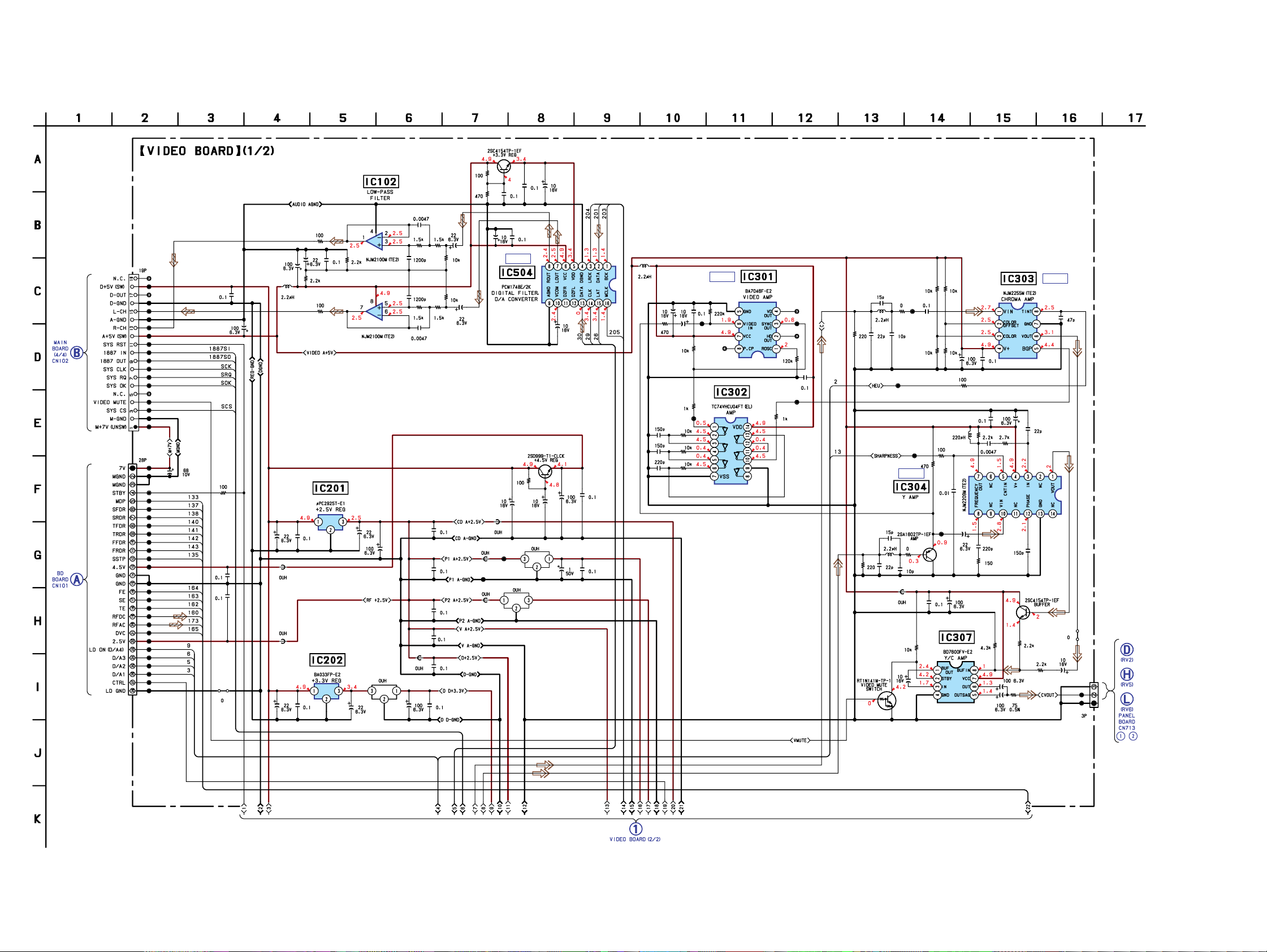
4-7. SCHEMATIC DIAGRAM — VIDEO SECTION (1/2) — • Refer to page 52 for IC Block Diagrams.
Q581
(Page
29)
(Page
19)
CN201
CN101
TP419
TP418
TP417
TP416
TP415
TP414
TP413
TP412
TP411
TP410
TP409
TP408
TP407
TP406
TP405
TP404
TP403
TP402
TP401
TP421
TP422
TP424
TP425
TP426
TP427
TP428
TP429
TP430
TP431
TP432
TP433
TP434
TP436
TP437
TP438
TP439
TP440
TP441
TP442
TP443
TP444
TP445
TP446
TP447
TP448
C257
C258
C255
C254
JW203
R202
C259
C201
FB252
FB251
C209
C116
L102
C202
C210
C114
R114
R152
R102
IC202
IC201
C115
R115
C214
IC102(1/2)
IC102(2/2)
C213
C203
FL201
C155
R159
C156
C106
R109
C105
FB201
C211
R158
R108
C212
C204
C205
C206
C207
C208
C154
R157
R107
C104
R581
R582 C584
C596
IC B/D
C221
FB501
FB503
TP197
TP198
FB502
IC504
FL504
C581
R201
C583
C222
FL503
Q201
C582
C597
C223
C547
C224
C548
L301
C307
C308
C309
C301
R302
R307
R308
R309
C303
R305
R306
TP304
C302
TP312
IC B/D
R301
TP313
IC302
IC301
R303
R310
TP311
TP309
TP305
TP310
C305
R321
Q370
C312
L311
C322
C321
L321
R312
C313C311R311
TP302
FB360
C364
TP301
TP306
IC B/D
TP303
Q301
R322
C323
R376
R323
R316
C314
R317
R327
C361
C329
R314
R315
L322
C360
IC307
R318
4
30
IC
C324
C318
C338
C328
C325
R374
C317
R324
R325R326
C366
C339
C326
C365
R375
IC303
R372
C327
Q302
R373
IC B/D
C363
C315
JW301
TP308
TP307
(Page 33)
(Page 36)
(Page 39)
CN301
(Page 25)
2424
Page 25
• Refer to page 17 for Waveforms.
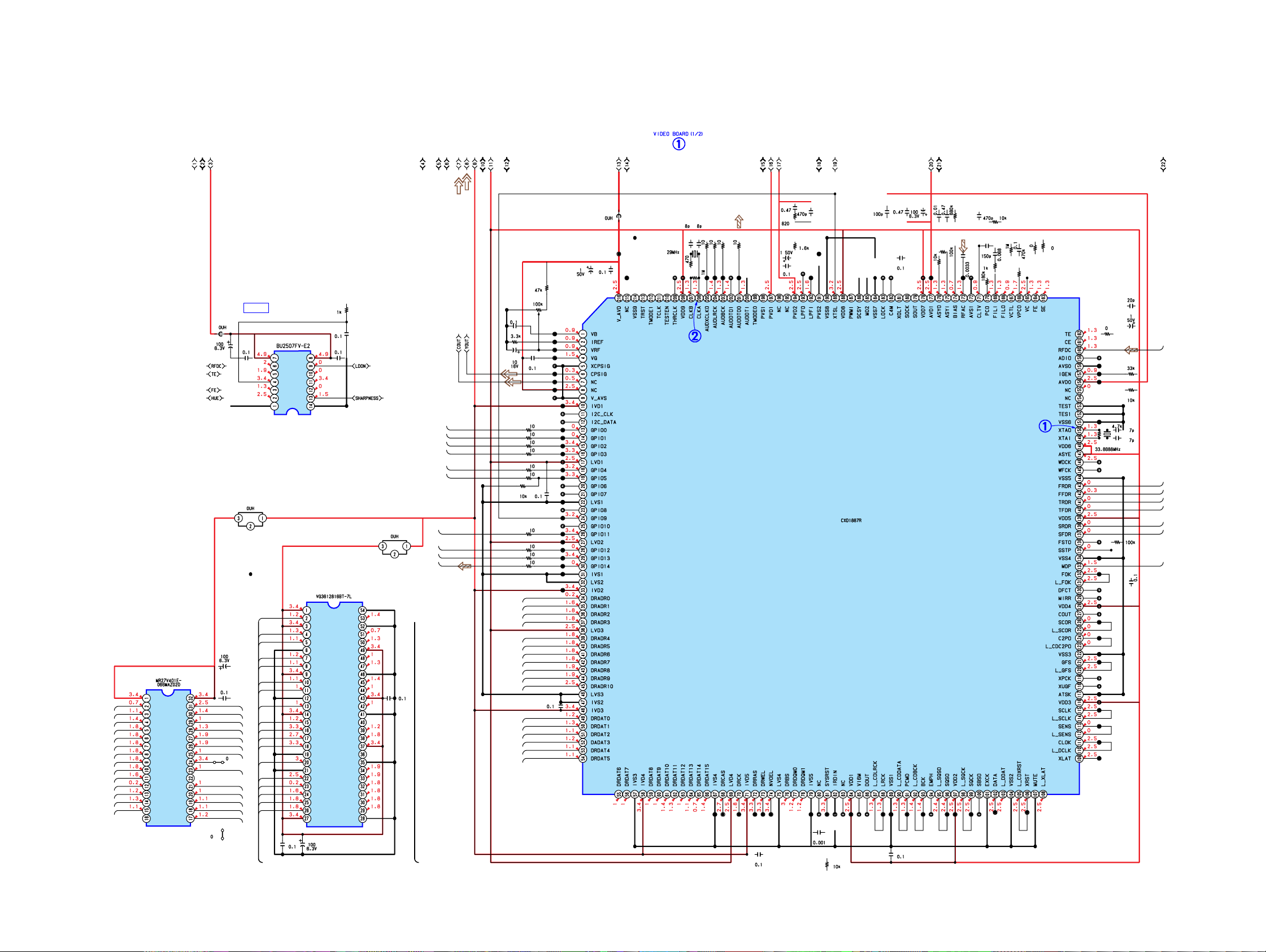
4-8. SCHEMATIC DIAGRAM — VIDEO SECTION (2/2) — • Refer to page 53 for IC Block Diagram.
IC B/D
HCD-RV2/RV5/RV6
25 25
Page 26
HCD-RV2/RV5/RV6
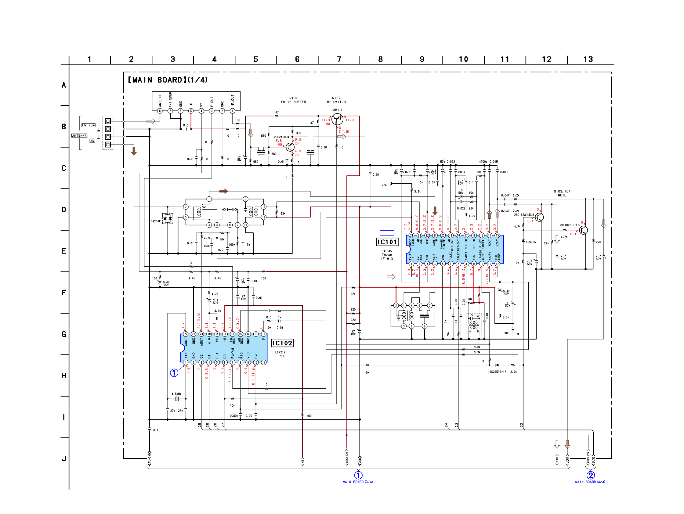
4-9. SCHEMATIC DIAGRAM — MAIN SECTION (1/4) — • Refer to page 54 for IC Block Diagram.
• Refer to page 17 for Waveform.
FE101
JK101
D101
C113
C100
C101
C112
JR112
R112R111
JR105
JR104
R113
C111
R114
R135
C116
R136
JR106 JR107
JR108
RB101
R115
C110
R104
C104
R117 C109
C114
C117
R106
C115
R102
CF101
R116
C118
R101
Q101
R103
R142
R121
C119
R122 C120
JR111
R108
R105C102
CF102
R109
C105
Q102
JR110
R120
R141
R124
C125
C128
RV101
IC B/D
IC101
C106
IFT101
C107
R140
R110
C108
C148
C143
C147
R147
C139
C138
C140
C146
C129
R148
R125
C130
C141
R131
R139
R132
T101
C142 C132
JR114
C126
C131R137
C151 R129
C150 R128
C133
C127
R127
C137
R144
R138
Q104
D109
C144
R134
R143
C136
Q103
R133
C135
C360
X101
IC102
R123
JR113
C122C121
R119
C123 C124
R118
(Page 28)
R146
R130
JR116
D108
R126
(Page 29)
2626
Page 27
4-10. SCHEMATIC DIAGRAM — MAIN SECTION (2/4) —
HCD-RV2/RV5/RV6
JR202
C260
JR201
R260
R269 R268
R220
R222
R265 R264 R276
C263
C264C265
Q262 Q261 Q264
D261
D262 D263
C266
C262
R271 R272
C226
R277R263R266R267R270
R226
C224
R275C227
C229
C267
C220
R262
R234
R239
R237
R235
R236
D205
R225
R212R214C222
C218
IC201
C235
R238C234
C230
R233
C219
R221
R219
C232
C233
C223
C225
R232
C221
C213
R211
R213
C214
C216
C215C217
R209
C212
R208R210
C211
R205
R207
R261
R206
C207
C208
C206
C200
C205
C202
C201
C203
C204
CN203
TP61
TP62
TP63
CN201
RV5/RV6
TP56
TP57
TP58
TP59
TP60
CN202
(Page 28)
R258
Q250
C253
R250
C252
C251
L250
Q251 Q252
C254
R251 R252
Q255
R253
Q256Q253 Q254
C255 R254
(Page 29)
27 27
Q257
R255
R256
Q258
C256
R257
Page 28
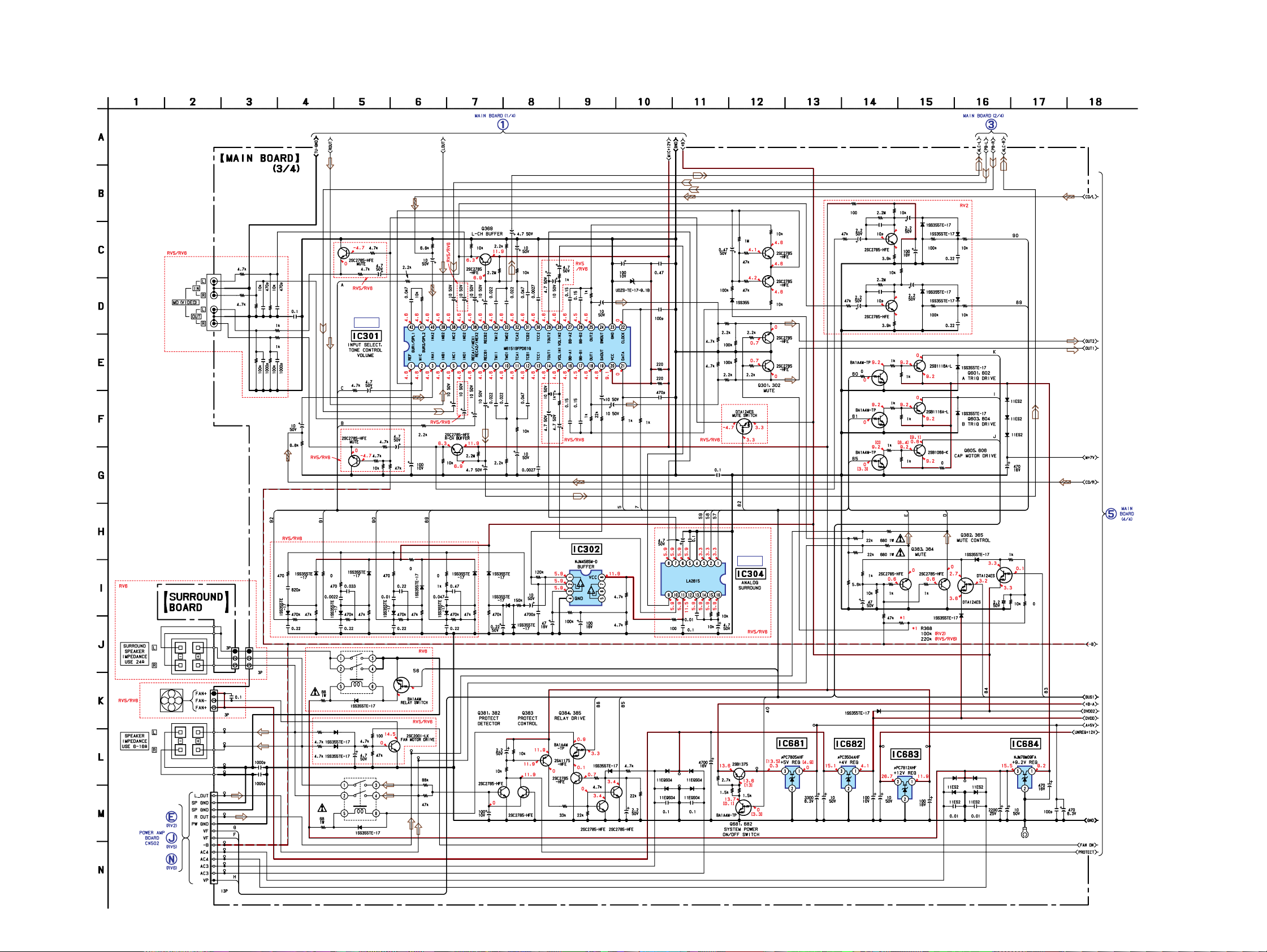
HCD-RV2/RV5/RV6
4-11. SCHEMATIC DIAGRAM — MAIN SECTION (3/4) — • Refer to page 54 for IC Block Diagrams.
(Page 27)(Page 26)
JK303
JK301
CN303
R301
R302
R304
R311
C351
C365
R321
R322
R303
R312
R323
D376
C352
C366
C322
C312
R340
C353
R325 R324
C344
R351
Q367
C305
R307
IC B/D
C304
R327
Q366
R308
R350
R330
D375
D377
JR322 JR323
C339
R326
D378
R341 R345
C345
C355C354
R339
C311
R305
R300
C394
R306
C306
C303
R376
JR321
R342
D380
C340
R344
C335
R346
D379
C356
R343 R354
D382
C309
C310
Q368
R316
D381
C341
R359 R347
C342
C301
C302
Q369
C307
C308
R314
C316
R317
R315
R313 R391
C321
C313
C320
C314
R318
D385
D384
C338
C324
C325
IC301
R353
C315
C317
R360
C318
D386
C331
C326
C328
C362
C323
C327
R352
C343
C359
C350
C358
C349
R310
C368
C367
R309
R357
C337
C332
C333
C334
IC302
C346
R319
R320
C347
C336
C348
R358
C357 C361
D301
R377
R378
R355
R356
C372
R348
R349
C371
C369
R392
C380
IC304
C379
C370
R331
R332
R390
C319
C421
R424
R379
R333
C384
R335
R336
R334
R429
R427
R428
D421
R337
R338
Q304
IC B/D
R425
R426
Q421
Q422
Q301
Q302
R396
R395
R407
R423
C388
C387
Q601
JR675
Q603
Q605
R422
R366
R421
R367
C363
Q308
Q307
C390
R406
R401
C389
R405
R362
R361
R404R402
C392
C393
R403
C391
R601
R602
R603
R604
R605
R606
Q363 Q364
R363R364
R368
R365
D388
D390
R412 R414
C395
D387
D389
R411
R413
C396
Q602
Q604
Q606
JR676
D361
Q365
D601
D602
D362
Q362
C364
R370
D691
D692
D693
C692
R369
(Page 29)
JR361
FAN961
JK302
(Page 43)
(Page 47)
(Page 51)
CN305
CN402
TP36
TP37
TP38
TP39
TP3
TP4
TP5
TP6
TP7
TP8
TP9
C378
CN304
C375
C376
R371
R372
R393
R394
RY372
D371
D374
D373
D372
R373
C377
RY371
R375
R374
Q388
Q371
TP49
R381
TP50
C381
Q381
R383
C382
Q382
R384
Q384
Q385
Q383
R385
R386
Q386
R387
D383
Q387
R389
D686
TP44
R388
C383
D681 D682
TP41
TP40
D683 D684
C683 C684
C685
R681
R682R382
Q682
Q681
R683
TP43
IC682IC681
C688C687 C689 C690
IC683
TP48TP78
D690
D689
TP42
C691
D687 D688
C693 C694
C697 C698
IC684
GND1
C699
C674
C675
2828
Page 29
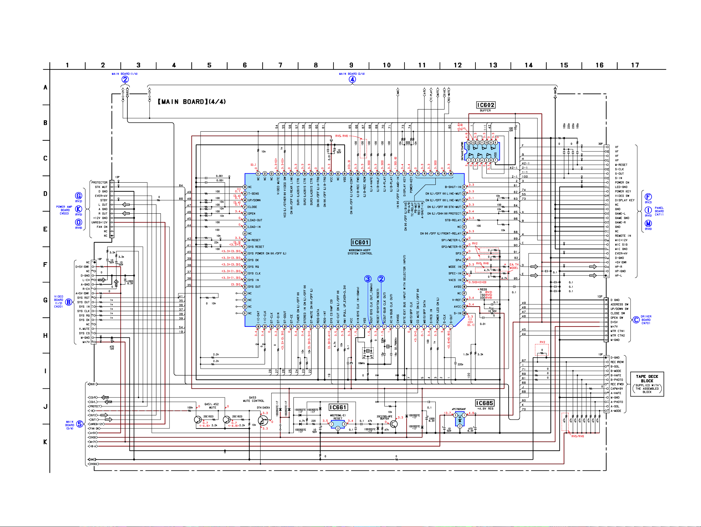
4-12. SCHEMATIC DIAGRAM — MAIN SECTION (4/4) — • Refer to page 17 for Waveforms.
HCD-RV2/RV5/RV6
(Page 43)
(Page 47)
(Page 51)
(Page 24)
CN102
(Page 26)
FB4
R619
R607
R608
R610
R612
R614
R615
R617
R616
C612
C613
R618
R694
TP76
R609
R611
R613
TP75
TP77
TP74
TP73
TP72
TP71
CN403
TP10
TP11
TP12
R329
R328
C451
C452
FB2
C671
JR690
FB3
TP21
R690
R691
R692
R693
R695
JR638
FB7
642
R
C610
C611
626
R
IC601
(Page 27)
628
627
R
R
C603
48
647
646
C645
C
C
C6
TP35
TP34
TP33
TP32
TP31
TP28
TP53
CN601
(Page 33)
(Page 36)
(Page 39)
CN103
JR679JR680
631
630
629
R
R
658
657
R
659
R660
R
R
R
IC602
TP67
R635
R638
R636
R637
R641
C602
C664
C601
R632
FB5
R633
R634
TP66
R680
R640
R639
C666
C657
C658
C659
C660
TP47
TP25
TP30
TP27
(Page 21)
TP26
TP29
C677
R653
R654
TP78
TP79
651
R
JR602
R646
R645
650
R649
R
C644
FB6
X602
JR601
655
R
TP69
644
R
C608
X601
607
C
P68
T
6
643
65
R
R
P67
T
R647 R648
C605
JR670
JR671
JR672
JR673
CN671
JR674
(Page 28)
R454
Q451 Q452
R451 R452
TP79
R453
Q453
JW336
C663
TP64
R663
D666
Q661
R665
R664
JR677
D
R661
R662
C661
D664
IC661
C662
JR678
D663 D665
662
661
D
D667
D668
C656
C665
C678
IC685
C679
TP80
5
672
671
676
679
677
678
R674
R
R
R67
R
R
R
R
29 29
Page 30
HCD-RV2/RV5/RV6
• Refer to page 32 for Semiconductor Location.
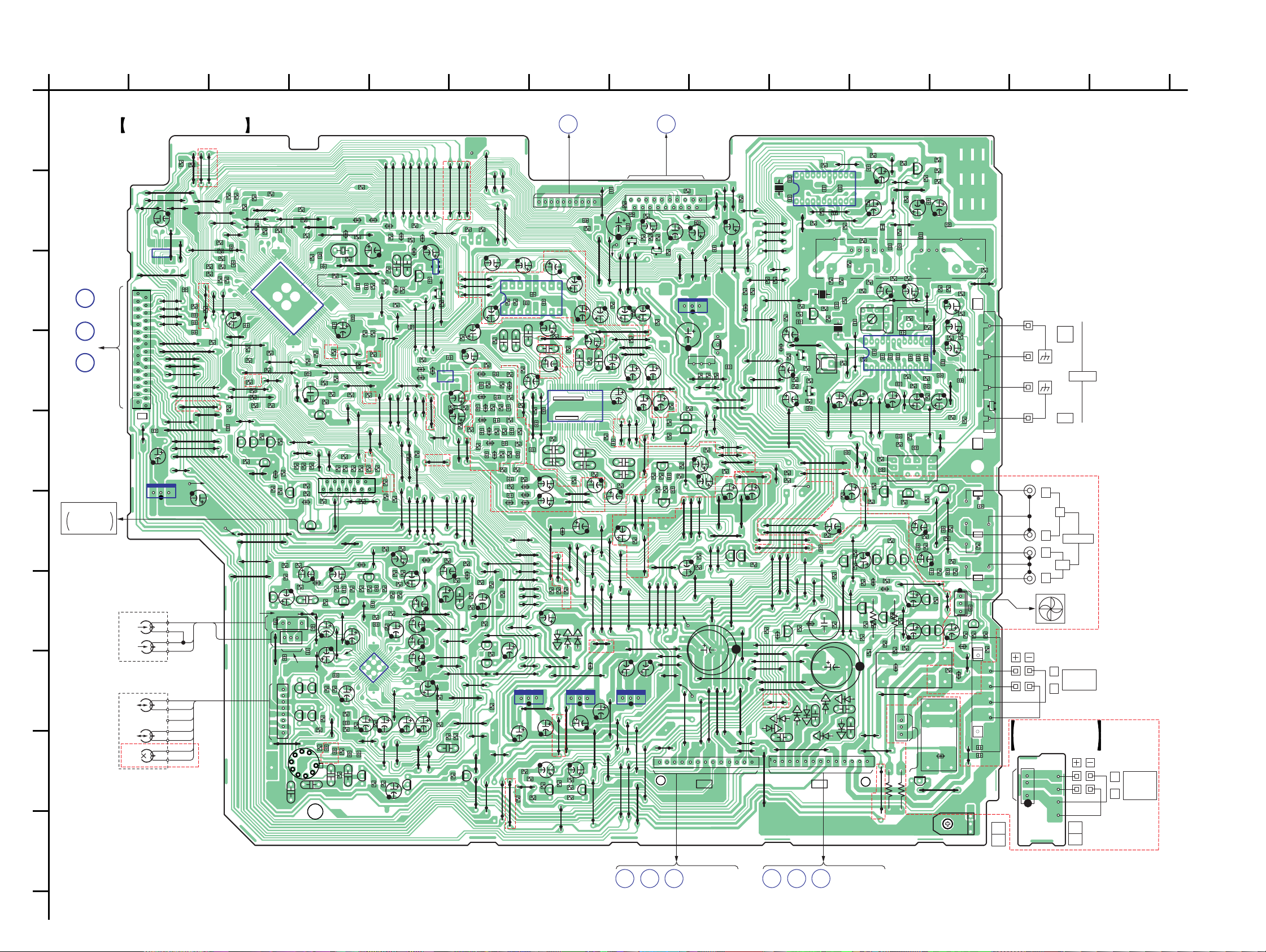
4-13. PRINTED WIRING BOARDS — MAIN SECTION — • Refer to page 16 for Circuit Boards Location.
A
B
C
D
E
F
G
H
I
J
1
(Page 31)
(Page 34)
(Page 37)
D
(RV2)
L
(RV5)
T
(RV6)
PANEL
BOARD
CN711
TAPE DECK BLOCK
SUPPLIED WITH
THE ASSEMBLED
BLOCK
234567891011121314
MAIN BOARD
RV5/RV6
JW232
R647
R648
JW233
JW234
JW235 JW236
C603
JW369
RV6
C648
JW287
JW289
JW290
JW291
JW296
JW297
JW302
JW237
C647
C646
C645
JW288
C678
JR679
JW292
JW293
W2
1
2
3
7
6
5
4
3
2
1
R608
R609
JW294
JW299
JW300
JW301
RV2
JW238
JW295
IC602
JW286
CN601
29
JW282
30
JW283
JW284
JW285
12
C657
JW288
C679
IC685
13
A DECK
PLAYBACK
R-CH
L-CH
R-CH
L-CH
ERASE
B DECK
RECORD/PLAYBACK/ERASE
RV6
JW231
JW241
R612
R613
R610
JW281
R642
JW230
JR680
JW240
JW240
R611
R607
JW280
W3
R614
JW239
R619
JW279
C610
JW278
RV5/RV6
JW273
JW272
R658
C666
Q603
JR675
JW305
R615
R617
JW243
C612
C613
50
51
C611
JW277
R626
JW275
R627
R629
JW304
B
E
JW336
JW337
RV5/RV6
R618
JW242
JW244
R692
R691
R659
R628
JW274
R630
R631 R660
R605
B
Q605
E
Q601
B
JW334
JW335
Q264
CLP1
R657
B
E
E
D601
R603
C201
R616
R651
JW276
Q606
B
E
CN201
3
JW338
CN202
JW368
L250
JW245
3031
IC601
JW271
R606
JW306
JW307
JR676
R671
E
B
R601
Q602
R276 R265
R275
R277
C267
JW339
3
CN203
RV2
C204
8
Q254Q253
1
C254
8180
FB4
R679
R602
1
R649
D602
B
C263
C227
E
B
E
B
JR602
R650
R632
C364
Q604
1
C203
R251
C251
JW246
R645
B
R604
C644
R634
Q362
JW308
R672
JR674
E
D261
C202
JW341
E
B
E
B
R225
R680
13
FB6
R644
X601
1
100
RV2
R636
R369
R370
E
JW309
JW333
C265
R263
E
R264
C205
JW340
C206
Q252Q251
R208
R252
C222
JW367
RV2RV2
C230
C252 C253
X602
C602
C601
JW258
JW259
JR672
R675
R676
CN671
JW332
Q261
R206
C229
JR361
JW331
JW342
C208
C212
R214
R210
R250
R693
JW228
D661
D667
D668
JW247
D662
C665
R646
R655
JW248
JW257
R635
JW270
C262
C200
JW343
R226
R663
JW249
R665
C608
C607
JR601
C664
FB5
JW251
R641
R640
R638
R639
RV5/RV6
JW260 JW261
R637
RV2
JW269
JW267
JW268
RV5/RV6
R674
R677
R678
RV2
JR671
1
JR677
JR673
R269
D262
JW330
Q262
B
E
R267
R266
R270
C264
B
R268
C221
R207
R261
JW344
C207
R205
RV2
IC201
C214
R262
R212
C216
JW366
C220
JW365
C219
E
R258
R255
Q250
B
JW227
R661
D666
JW250
JW266
JR670
JR678
R271
R213
C211
JW364
C256
JW226
JW225
D664
R662
C662
C663
R656
JW252
C605
D384
D385
JW264
JW265
JW310
JW311
JW325
JW324
R260
C260
C266
R272
JR201
R211
C217
C224 C218
JW363
R643
Q661
R664
JW253
JW263
C213
E
B
JW224
D665
EB
R353
RV5/RV6
JW262
RV5/RV6
R633
JW312
JW323
D263
R232
JW362
Q257
JW223
D663
JW254
RV5/RV6
JW313
R306
JW322
JW326
JW345
R209
C223
C215
C232
JW361
JW222
JW221
JW255
D386
C343
R356
JW154
JW314
JW321
JW327
C233
C234
JW329
JW356
C656
JW256
IC302
C346
JW347
JW351
JW352
R235
C226
RV5/RV6
JW220
C661
IC661
Q453
R453
C362
14
85
JW320
R234
JW350
JR202
R220
JW219
R354
R355
JR321
JW315
JW319
D205
R236
JW353
JW355
R222
Q258
R256
R233
CLP2
JW218
R654 R653
JW212
JW211
JW210
C338
C323
D376
C344
D377
C345
R357
D379
JW316
JR322
RV5/RV6
JW318
JW317
R237
R219
C225
R221
Q255
E
E
JW354
JW357
JW358
JW359
E
B
JW360
R352
C335
D380
DRIVER BOARD
C
CN701
(Page 20)
JW217
JW216
JW215
110
CN103
FB7
JW213
JW214
C316
C315
1
IC304
C370
R379
R390
C384
D378
D381
C342
JW328
JW124
C380
C353
R325
C354
R341
C355
D382
RV2
JW346
R238
JW349
B
R253
B
Q256
JW125
16
R320
C334
R323
R324
R326
R343
R344
C356
R347
R359
R413
C395
R411
C396
D389 D387
JW151
JW149
R239
C235
R257
JW122
RV5/RV6
R345
C318
C328
C326
C332
R358
C350
C336
D375
R378
JW155
R377
C339
R342
JW156
JW157
C372
JR323
C340
R346
C361
C341
C333
R414
C392
R412
D388
D390
C391
JW153
JW152
JW150
JW148
JW147
R254
JW146
JW348
C692
C255
JW131
JW130
JW127
11
3
JW126
C698
C699
RV5/RV6
C347
R331
R333
JW120
R335
R368
R337
JW121
C358
C379
RV2
21
C371
22
R319
JW145
D692
E
B
RV5/RV6
8
9
R360
JW191
C337
JW144
R348
R349
RV5/RV6
JW129
JW117
JW118
R332
R336
R338
Q301
JW119
C359
R310
IC301
R425
JW158
JW159
D301
JW143
R392
D691
JW128
1
C348
R334
R694
C369
C368
C324
C331
C357
JW142
JW141
D693
C689
E
B
JW192
C308
R318
C320
1
42
C327
R391
C349
JW138
JW139
JW140
JW132
RV5/RV6
D686
3
C688
JW115
Q302
JW116
C314
RV5/RV6
R300
JW137
JW114
C675
JW209
W1
JW193
R305
JW189
C303
C394
C321
C317
JW135
JW136
JW113
C658
R690
JW194
C311
JW190
R327
JW187
JW162
RV5/RV6
C393
JW134
C691
IC683IC682IC684
JW112
JW111
1
FB2
Q451
JW195
C304
JW163
C325
R317
JW133
JW110
JW109
C674
JW196
C312
R339
JW188
C313
JW164
JW160
JW101
C690
JW108
JW107
R329
JW186
JW165
JW161
R407
JW096
3
JW106
B
CN102
JR690
C451
R452
R451
Q452
R340
C307
C367
R314
JW166
R313
Q308
EE
R406
R404
R405
R403
EE
Q307
JW095
JW098
JW099
JW100
JW102
JW103
JW104
JW105
1
VIDEO BOARD
CN201
(Page 22)
R695
18
JW208
C425
C671
R328
JW198
JW199
IC681
1
C687
Q681
R683
R681
JW183
JW184
R309
RV5/RV6
R426
Q368
EE
EE
Q369
R396
R402
C390
JW167
R401
C387
C389
JW168
JW169
JW170
C421
R429
R427
JW093
JW097
W1
D694
W3
JW069
CN403
19
FB3
JW200
3
C388
JW092
JW094
C685
JW067
C659
JW179
R395
JW207
JW201
R682
JW182
JW181
JW180
JW178
JW171
JW172
JW070
JW066
JW061
JW206
C677
Q682
C660
JW177
JW176
JW091
Q421
JW090
JW065
JW205
JW202
E
B
JWO64
JW062
JW204
D108
RV2
JW175
C310C309
JW173
E
B
Q422
R454
JW203
R126
JW021
JW022
JW024
RV5/RV6
JW076
RV5/RV6
JW063
D682
13
JW015
R148
JW023
RV5/RV6
R428
JW078
JW077
JW075
JW010
JW011
JW012
JW013
C136
JR638
JW074
JW073
JW071
JW060
X101
JW014
R120
C144
C135
JW086
JW085
D684
R123
JW020
R138
D109
R144
R143
JW174
JW089
JW088
JW087
JW084
D361
JW072
C684
CN402
C122C121
R103
R105
JW037
R315
JW083
B
Q365
E
1
C102
R128
Q104
R316
JW082
JW059
JW009
JW025
R134
R367
D681
R136
R121
B
E
JW081
D362
D690
D683
CF101
Q101
R133
Q103
R129
C151
JW038
JW041
W2
JW080
R119
IC102
JW007
JW008
R102
RV101
R307
C322
JW079
C363
D689
C123
R104
CF102
C305
C697
C683
R108
C106
JW036
C319
Q387
R424
R366
JW006
C118
C119
C105
R140
R308
JW047
D687
11
1222
JR112
JR108
R106
JR111
C128
JW026
JW035
C306
JW046
E
B
JW048
D688
JR105
R109
R110
JW027
C108
JW039
R388
C693
R386
R389
R365
C694
R118
C116
R135
R101
IFT101
1
24
JW034
R376
JW043
C383
E
Q364
B
R363
R422
JW058
13
RV5/RV6
C117
C124
C107
C143
R142
C111
JW040
Q386
D383
JW057
JR104
C148
C146
JW033
R117
R330
R387
B
E
R385
Q363
B
R364 R362
R421
JW056
JW002
JW004
C101
C104
IC101
R139
E
B
Q385
D421
E
JW053
JW005
JW019
C126
C147
C109
Q304
B
E
R423
R361
R381
D372
CN304
R393
Q102
JW001
JW003
R111
C120
JR106JR107
R125
C139
JW032
Q366
B
R350
Q384
JW049
JW051
R383
3
1
R394
RV6
JR110
B
E
R122
T101
R132
C138
C110
RB101
R302
B
E
C382
C381
R382
RY371
E
C142
C113
C125
E
C302
C351
JR114
C132
R137
R115
R112
JW018
12
13
R131
R351
C352
Q381
B
Q388
R116
C115
C100
R146
C131
C150
C141
C140
E
JW044
R304
C301
R303
B
E
Q383
B
E
Q382
R372
RY372
D373
JW055
GND1
C127
JW031
JW030
Q367
R384
R114
R113
C114
C112
R141
R124
C137
JW017
C129
R147
B
JW045
C366
R322
R321
CN305
C365
1
JW069
3
B
E
C377
1-685-088-
FE101
C133
JW028
JW029
R312
R373
D371
D374
JR116
R130
C130
JR113
R311
E
JW052
JW054
R127
JK301
JK303
Q371
JR102
JW016
C360
R301
C378
JK101
CLP3
B
R374
C376
C375
D101
R375
R371
SURROUND
BOARD
CN303
3
2
1
11
(11)
1-685-089-
R
L
R
L
FAN961
IN
OUT
L
R
FM
75Ω
ANTENNA
AM
RV5/RV6
MD(VIDEO)
SPEAKER
IMPEDANCE
USE 6-16Ω
11
(11)
JK302
JK101
JK301
R
L
JK303
SURROUND
SPEAKER
IMPEDANCE
USE 24Ω
F
O
(RV5)W(RV6)
(RV2)
(Page 40) (Page 44) (Page 48) (Page 40) (Page 44) (Page 48)
POWER AMP
BOARD
CN503
E
(RV2)N(RV5)V(RV6)
POWER AMP
BOARD
CN502
3030
Page 31

4-14. PRINTED WIRING BOARDS — PANEL SECTION (HCD-RV2) — • Refer to page 16 for Circuit Boards Location.
HCD-RV2/RV5/RV6
A
B
C
D
E
F
G
H
I
1
DISC 2
S710
DISC 3
S711
OPEN/CLOSE
Z
D
MAIN
BOARD
CN601
(Page 30)
234567891011121314
PANEL BOARD
S708
DISC 1
R708
JK701
R712
R710
R711
JW710
JW711
C736
R709
JW703
JW709
JW706
VOLUME
DISC SKIP/
EX-CHANGE
JW724
VR701
C734
C770
S709
CN711
JW780
C737
PHONES
• Semiconductor Location
Ref. No. Location
D712 E-6
D713 C-4
D714 E-12
D715 E-12
D716 C-9
IC701 C-6
IC702 E-9
IC703 E-7
IC704 E-11
LED701 A-11
JW701
JW702
C703
R713
S712
JW706
JW732
JW766
JW709
C735
WIRE702
JW758
(CHASSIS)
Ref. No. Location
LED702 D-11
LED703 C-11
LED704 B-11
LED705 C-11
Q701 C-10
Q702 B-10
Q703 B-10
Q704 B-10
Q705 B-10
Q706 E-5
Q711 E-6
C710
JW720
JW707
R750
JW721
JW708
JW790
JW761
JW730
R768
JW781
FB701
R763
R759
JW722
JW774
R762
R760
R758
R761
JW713
R749
JW773
JW725
JW732
C721
C711
JW772
JW714
JW733
JW726
R748
R714
R752
R753
C701
JW735
D713
JW727
R715
JW715
JW712
JW734
JW736
R803
R802
15 10 15 20 25 30 35 40
JW737
FLD701
JW743
61 60
C723
C722
R777
C749
IC703
C742
JW741
JW745
C777
JW779
C750
916
81
R774
R781
R779
R773
C747
R747
R780
R778
C741
R775
R792
JW731
JW771
JW719
Q706
EB
JW718
JW717
JW792
R745
R740
R764
C713
C720
C716
RES701
JW728
R772
R771
80
1
JW740
R765
JW739
JW738
Q711
EB
C739 C738
IC701
41
40
20
21
JW729
R776
C746
R777
D712
CN712
17
KEY BOARD
G
CN715
(Page 32)
REMOTE BOARD
RM701
1
1
CN702
3
1-685-097-
3
11
(11)
MIC BOARD
CN704
3
WIRE703
1
C724
C780
C748
C744
C725
C751
C740
R791
JW744
C726
C727
JW770
JW760
C752
C745
3
4
(CHASSIS)
C728
C766
R787
C759
5
7
2
1
C729
C763
C758
C730
C731
R782
IC702
1
C754
R783
C760
6
1-685-098-
C732
D716
R790
C733
R769
C762
C765
11
(11)
C702
JW746
C761
R789
JW753JW752
JW747
C756
R784
Q704
Q705
Q703
Q702
Q701
CN701
C704
C775
R786
JK702
MIC
EB
EB
EB
EB
EB
R795
R739
JW751
31
C774
C755
C764
C705
R796
C757
R788
JW756
JW755
JW754
JW750
R800
R785
JW750
R701
R707
LED704
CD
LED705
TUNER
/BAND
LED703
TAPE A/B
LED702
GAME
R799
C718
R801
C719
CN713
41
C753
C767
D714
IC704
1
C771
C776
31
VIDEO OUT BOARD
JW757
R767
C781
VR702
ECHO
LEVEL
CN703
VR703
MIC
LEVEL
CN605
LP601
LED701
C772
I/
R703
R704
R751
D715
R755
C779
R702
R705R706
TAPE A/B
S704
GAME
WIRE701
(CHASSIS)
S716
S702
TUNER
/BAND
S703
I /
JW775
JW759
JK704
1-685-096-
-1
-2
-3
S701
CD
C707
1-685-091-
11
(11)
C
R744
R743
C706
R741R742
BOARD
JK602
VIDEO
L
R
11
(11)
VIDEO
CN301
VIDEO OUT
GAME
INPUT
AUDIO
(Page 22)
JK704
31 31
Page 32

HCD-RV2/RV5/RV6
• Semiconductor Location (Main Board)
Ref. No. Location
D101 D-12
D108 C-9
D109 D-10
D205 G-6
D261 G-4
D262 F-4
D263 F-5
D301 F-7
D361 G-10
D362 G-10
D371 G-12
D372 H-11
D373 I-12
D374 H-12
D375 D-6
D376 D-6
D377 D-6
D378 D-6
D379 E-6
D380 E-6
D381 E-6
D382 E-6
D383 G-11
D384 D-5
D385 D-5
D386 D-5
D387 F-6
D388 E-6
D389 F-6
D390 F-6
D421 G-11
D601 E-3
D602 F-4
D661 B-4
D662 B-4
D663 B-5
D664 B-5
D665 C-5
D666 C-5
D667 B-5
D668 B-5
D681 H-10
D682 H-9
D683 H-10
D684 H-10
D686 H-7
D687 I-10
D688 H-10
D689 I-10
D690 H-10
D691 G-7
D692 G-7
D693 G-7
IC101 D-11
IC102 B-10
IC201 H-5
IC301 D-7
IC302 D-5
IC304 C-6
IC601 C-3
Ref. No. Location
IC602 C-2
IC661 C-5
IC681 C-9
IC682 H-7
IC683 H-8
IC684 H-6
IC685 E-2
Q101 C-10
Q102 B-11
Q103 D-10
Q104 D-10
Q250 I-4
Q251 H-4
Q252 H-4
Q253 H-4
Q254 H-4
Q255 G-6
Q256 H-6
Q257 I-5
Q258 I-6
Q261 G-4
Q262 G-4
Q264 G-3
Q301 I-7
Q302 I-7
Q304 F-11
Q307 F-8
Q308 E-8
Q362 E-4
Q363 G-11
Q364 G-11
Q365 G-10
Q366 F-11
Q367 E-12
Q368 E-8
Q369 E-8
Q371 G-12
Q381 G-11
Q382 G-12
Q383 G-11
Q384 F-11
Q385 F-11
Q386 F-11
Q387 F-10
Q388 I-11
Q421 F-9
Q422 F-9
Q451 B-8
Q452 C-8
Q453 C-5
Q601 E-3
Q602 F-3
Q603 E-3
Q604 F-4
Q605 E-3
Q606 E-3
Q661 C-5
Q681 D-9
Q682 D-9
4-15. PRINTED WIRING BOARD — KEY SECTION (HCD-RV2) — • Refer to page 16 for Circuit Boards Location.
1
2345678910
A
KEY BOARD
B
C
D
E
S736
CD SYNC
S737
REC
PAUSE/START
S726
>
R736
R725
R726
S740
MOVIE EQ
R735
S739
GROOVE
R754
EFFECT ON/OFF
R738
R737
S727
M +
S725
ALBUM+
R724
S738
R723
R727
S724
GAME MIXING
GAME MIXING
x
LED707
S732
S728
G
S742
DISPLAY
S717
GAME EQ
R728
S723
X
R722
R729
S718
MUSIC EQ
R717
R716
R731
R730
S729
– m
S730
ALBUM-
17
CN715
G
S731
.
1-685-092-
11
(11)
PANEL BOARD
CN712
(Page 31)
3232
Page 33

• Refer to page 17 for Waveform.
4-16. SCHEMATIC DIAGRAM — PANEL SECTION (HCD-RV2) — • Refer to page 55 for IC Block Diagrams.
HCD-RV2/RV5/RV6
IC B/D
IC B/D
33 33
Page 34

HCD-RV2/RV5/RV6
4-17. PRINTED WIRING BOARDS — PANEL SECTION (HCD-RV5) — • Refer to page 16 for Circuit Boards Location.
A
B
C
D
E
F
G
1
S709
DISC 2
S710
DISC 3
S711
OPEN/CLOSE
Z
L
MAIN
BOARD
CN601
(Page 30)
234567891011121314
PANEL BOARD
S708
DISC 1
R708
JW762
R709
CN711
JW780
C737
R711
R712 R710
JW710
JW711
C736
JW703
JW709
DISC SKIP/
VR701
VOLUME
C734
C770
JW701
S712
EX-CHANGE
JW705
JW706
C735
WIRE702
JW761
JW702
R713
JW764
JW765
JW712
R749
R750
JW721
JW720
R748
JW763
JW747
JW758
JW713
(CHASSIS)
C710
JW723
JW722
JW708
C703
JW724
JW707
FB701
R768
R745
R752
JW725
JW730
R759
JW726
JW719
Q706
EB
JW769
C701
C721
R761
JW727
R753
JW766
JW714
R763
JW733
R762
JW781
TUNER MEMORY/
PLAY MODE
JW767
JW768
JW715
JW791
R760
R758
C711
R803
R802
R805
D713
JW728
JW718
R740
JW717
JW792
JW770
JW737 JW777
JW734
C720
C716
R764
JW782
R765
RES701
C713
S713
JW729
R714
EB
Q708
R746
CN712
17
M
JW738
JW729
JW728
JW774
JW773
JW772
JW771
R715
KEY BOARD
CN715
(Page 35)
80
1
JW740
JW739
S714
FM MODE/
REPEAT
Q711
EB
R772
R771
C739
JW778
61 60
IC701
20
21
R770
S715
DIRECTION
/EDIT
R776
D712
C738
C743
41
40
FLD701
JW735
R777
JW702
C749
IC703
JW745
JW741
SPECTRUM
S707
C750
C742
R774
C722
R747
R781 R780
R779
C740
916
R778
81
C741
R773
C747
C723
C724
C725
C726
Q701
C777
S742
DISPLAY
JW760
C751
C748
C752
C763
C744 R787
R775
R792
C780
C727
C728
EB
JW783
R790
C762
C766
C759
R791
JW753JW780JW779
C729
JW742
R782
IC702
1
C730
JW756
C754
R783
C731
JW755
D716R769
C732
R796
C733
JW785
JW793
C765
C761
C756
R784
C760C758C745
C708
C705
JW786
JW746
C704
C775
R786
R795
R789
CN701
31
C774
C755
C702
EB
C773
C764
C718
R788
EB
EB
Q703
EB
EB
JW751
R785
Q707
Q702
JW748
R799
R801
C757
Q704
Q705
IC704
1
C719
CN713
R800
41
C753
JW750
C767
LED701
I/
R701
R739
R703
S706
WIRE701
R702
R705
S704
MD(VIDEO)
(CHASSIS)
LED704
CD
LED705
TUNER
/BAND
LED703
TAPE A/B TAPE A/B
LED706
MD(VIDEO)
LED702
GAME
D714
D715
C776
C771
C781
R704
R707 R706
R751
R767
KARAOKE PON
R755
C772
VR702
ECHO
LEVEL
CN703
31
VR703
S716
S702
TUNER
/BAND
S703
S705
GAME
C707
JK704
I /
S701
CD
R744
R743
C706
JW759
R741R742
11
(11)
VIDEO
L
R
AUDIO
GAME
INPUT
JK704
-1
-2
-3
1-685-099-
H
JK701
PHONES
MIC
LEVEL
VIDEO
K
BOARD
(Page 22)
CN301
REMOTE BOARD
• Semiconductor Location
Ref. No. Location
D712 F-7
I
D713 C-5
D714 E-11
D715 E-11
D716 D-9
IC701 C-6
IC702 F-9
IC703 F-7
IC704 E-11
Ref. No. Location
LED704 B-11
LED705 C-11
LED706 D-11
Q701 D-9
Q702 D-10
Q703 C-10
Q704 B-10
Q705 C-10
Q706 E-4
RM701
1
1
3
3
CN702
1-685-105-
11
(11)
MIC BOARD
CN704
3
WIRE703
1
3
4
(CHASSIS)
5
7
6
2
1
1-685-106--
11
(11)
JK702
MIC
VIDEO OUT BOARD
CN605
LP601
1-685-104-
11
(11)
JK602
VIDEO OUT
Q707 C-10
LED701 A-12
LED702 D-11
Q708 F-5
Q711 E-6
LED703 C-11
3434
Page 35

4-18. PRINTED WIRING BOARD — KEY SECTION (HCD-RV5) — • Refer to page 16 for Circuit Boards Location.
HCD-RV2/RV5/RV6
A
B
C
D
E
1
2345678910
KEY BOARD
S736
CD SYNC
R735
R736
R737
PAUSE/START
S737
REC
S726
>
S740
MOVIE EQ
S738
P FILE
R725
R726
PANEL BOARD
M
CN712
17
CN715
S739
ENTER
R738
S727
M +
S725
ALBUM+
R754
LED708
ENTER
S734
B
R727
(Page 34)
R722
R724
R723
R728
S724
x
R734
R733
S735
v
S733
S728
gG
S718
MUSIC EQ
S732
b
R732
V
S723
X
R729
R731
R730
R717
R716
R718R719
S719
EFFECT ON/OFF
S717
GAME EQ
GAME MIXING
S729
– m
S730
ALBUM-
S720
S722
PICTURE EFFECT
S721
GROOVE
R721
R720
LED707
GAME MIXING
S731
.
1-685-100--
11
(11)
35 35
Page 36

HCD-RV2/RV5/RV6
• Refer to page 17 for Waveform.
4-19. SCHEMATIC DIAGRAM — PANEL SECTION (HCD-RV5) — • Refer to page 55 for IC Block Diagrams.
FLD701
(Page 24)
IC B/D
JK702
TP701
CN704
TP702
R764
R763
R761
R759
VR701
TP703
TP704
TP705
C721
R753
R752
C720
TP706
C713
C710
C711
R750
R749
TP707
RES701
C716
CN703
TP708
C757
TP709
TP710
C755
TP715
TP714
TP713
TP712
TP711
R765
D713
R762
R760
R758
C735
C734
R768
R786
C754
R785
C756 R784 R783
TP716
TP718
TP717
R748R747
IC702(1/2)
TP719
TP720
R787
C759
TP721
TP722
C758
TP723
TP724
TP725
TP726
R788
TP727
TP728
TP729
IC701
TP730
R776
TP732
D712
TP733
C722
R777
TP734
C723
C748
TP735
C724
TP736
C725
TP737
C726
C749
TP738
C727
TP739
C728
R781
TP740
C729
R779
TP741
C730
C750
C751
TP742
C731
R780
TP743
C732
TP731
C733
C708
C753
R782
C752
C702
C701
TP744
R803
R802
R805
R751
LED702
Q702 Q703 Q704 Q705 Q707 Q706 Q708
R708 R709 R710 R711 R712 R713 R714 R715
S708 S709 S710 S711 S712 S713 S714 S715 S716
R701 R702 R703 R704 R705 R706 R707
S701 S702 S703 S704 S705 S706 S707 S742
FB701
C703
CN712
LED706LED705LED704LED703
R745 R746
R767
R739
C771
C781
D715
R740
LED701
Q701
IC704
C777
WIRE702
R799
C775
C773
R801
C770
714
D
C772
C707
R743
R744
R769
D716
C774
C719C718
C776
R796
R800
R755
R741
R742
C706
TP766
TP767
C737
C736
C705
C704
TP771
TP772
TP773
TP774
TP745
TP746
TP749
TP750
TP751
TP752
TP753
TP754
TP755
TP756
TP758
TP759
TP760
TP748
TP747
TP761
TP762
TP763
TP764
TP769
TP768
TP770
TP651
CN713
JK704
CN711
CN701
JK701
CN702
CN605
JK602
(Page 29)
RM701
C767
C765
C760
VR703
C764
R789
R795
C761
C745
VR702
R790
C762
R775
C766
IC702(2/2)
C780 R792
R791
C763
R771
R772
C744
R774
C739
R770
R773
C738
C742
Q711
C740
C741
IC703
R778
C747
IC B/D
CN715
LED708 LED707
3636
R735 R736 R737 R738 R754
S736 S737 S738 S739 S740
R722 R723 R724 R725 R726 R727 R728 R729 R730 R731 R732 R733 R734
S723 S724 S725 S726 S727 S728 S729 S730 S731 S732 S733 S734 S735
R716 R717 R718 R719 R720 R721
S717 S718 S719 S720 S721 S722
Page 37

4-20. PRINTED WIRING BOARDS — PANEL SECTION (HCD-RV6) — • Refer to page 16 for Circuit Boards Location.
HCD-RV2/RV5/RV6
A
B
C
D
E
F
G
1
PANEL BOARD
S708
DISC 1
S709
DISC 2
S710
DISC 3
S711
OPEN/CLOSE
Z
T
MAIN
BOARD
CN601
CN711
JW780
C737
234567891011121314
R711
R712 R710
JW710
JW711
C736
R708
R709
JW703
JW709
VOLUME
JW701
S712
DISC SKIP/
EX-CHANGE
JW705
JW706
VR701
C734
C735
WIRE702
C770
JW762
JW761
JW764
JW702
R713
JW765
JW720
JW763
JW747
JW713
JW712
(CHASSIS)
R749
C710
R750
JW721
R748
JW758
JW723
JW722
JW708
C703
JW724
JW707
FB701
R768
R745
R752
JW725
JW730
R759
JW726
JW719
Q706
EB
JW769
C701
C721
R761
JW727
R753
JW766
JW714
R763
JW733
JW781
TUNER MEMORY/
PLAY MODE
JW767
JW768
JW715
JW791
R762
R760
R758
C711
R803
R802
R805
D713
JW728
JW718
R740
JW717
JW792
JW770
JW737 JW777
JW734
C720
C716
R764
JW782
R765
RES701
C713
S713
JW729
R714
EB
Q708
R746
CN712
17
U
JW738
JW729
JW728
JW774
JW773
JW772
JW771
R715
KEY BOARD
CN715
80
1
JW740
JW739
S714
FM MODE/
REPEAT
Q711
EB
R772
R771
C739
JW778
61 60
IC701
20
21
R770
S715
DIRECTION
/EDIT
R776
D712
C738
41
40
FLD701
JW735
R777
C749
IC703
JW745
JW741
SPECTRUM
C742
R747
S707
C750
R774
C722
R781 R780
R779
C740
R778
C741
R773
C747
C723
C724
C725
C726
Q701
C777
S742
DISPLAY
JW760
C751
C748
C752
C763
C744 R787
R775
R792
C780
C727
C728
EB
JW783
R790
C762
C766
C759
R791
JW753JW780JW779
C729
JW742
R782
1
C730
JW756
IC702
C754
R783
C731
JW755
D716R769
C732
R796
C733
JW785
JW793
C765
C761
C756
R784
C760C758C745
C708
C705
JW786
JW746
C704
C775
R786
R795
R789
CN701
31
C774
C755
C702
EB
C764
C718
C773
Q703
EB
JW751
R785
R788
EB
EB
EB
JW748
R799
Q704
Q705
Q707
Q702
R801
C757
C719
R800
C753
JW750
C767
R739
LED704
CD
LED705
TUNER
/BAND
LED703
TAPE A/B TAPE A/B
LED706
MD(VIDEO)
LED702
GAME
D714
IC704
1
C776
C771
C781
CN713
41
LED701
I/
R701
R751
R767
R755
D715
C772
VR702
ECHO
LEVEL
CN703
31
VR703
R703
R702
R704
R705
MD(VIDEO)
R707 R706
S706
KARAOKE PON
WIRE701
S716
S702
TUNER
/BAND
S703
S704
S705
GAME
C707
JK704
(CHASSIS)
JW759
-1
-2
-3
S701
CD
R741R742
1-685-107-
R744
R743
C706
11
(11)
VIDEO
L
R
AUDIO
GAME
INPUT
JK704
H
JK701
PHONES
REMOTE BOARD
RM701
I
1
CN702
1-685-113-
3
11
(11)
1
3
MIC BOARD
CN704
3
WIRE703
1
3
4
(CHASSIS)
5
7
6
2
1
11
1-685-114-
(11)
JK702
MIC
MIC
LEVEL
VIDEO OUT BOARD
CN605
LP601
1-685-112-
11
(11)
VIDEO
S
BOARD
CN301
JK602
37 37
Page 38

HCD-RV2/RV5/RV6
4-21. PRINTED WIRING BOARD — KEY SECTION (HCD-RV6) — • Refer to page 16 for Circuit Boards Location.
A
B
C
D
E
1
2345678910
KEY BOARD
S741
SPEAKER
MODE
CD SYNC
R756
R735
R736
R737
PAUSE/START
S736
S737
REC
S726
>
S740
MOVIE EQ
S738
P FILE
R725
R726
(Page 37)
PANEL BOARD
U
CN712
17
CN715
S739
ENTER
R738
S727
M +
R754
LED708
ENTER
S725
ALBUM+
S734
B
R727
R724
R722
R723
S724
x
R734
R733
R728
S735
v
S733
V
S728
gG
R732
S732
b
S723
X
R729
S718
MUSIC EQ
R717
R718
R719
R731
R716
R730
S719
EFFECT ON/OFF
S717
GAME EQ
GAME MIXING
S729
– m
S730
ALBUM-
PICTURE EFFECT
GROOVE
S720
S722
S721
R720
S731
.
R721
LED707
GAME MIXING
1-685-108-
11
(11)
3838
Page 39

• Refer to page 17 for Waveform.
4-22. SCHEMATIC DIAGRAM — PANEL SECTION (HCD-RV6) — • Refer to page 55 for IC Block Diagrams.
FLD701
HCD-RV2/RV5/RV6
(Page 24)
IC B/D
JK702
TP701
CN704
VR701
TP702
R764
R763
R761
R759
TP703
TP704
TP705
C721
C720
R753
R752
TP706
TP707
C713
C710
C711
R750
R749
CN703
TP708
RES701
C716
C757
TP709
TP710
C755
C756
TP711
C735
C734
R785
TP712
R768
R786
TP713
D713
R762
R760
R758
C754
R784
TP714
R765
TP715
TP716
R783
TP718
TP717
R748R747
IC702(1/2)
TP719
TP720
R787
C759
TP721
TP722
C758
TP723
TP724
TP725
TP726
R788
TP727
TP728
TP729
IC701
TP730
R776
TP732
D712
TP733
C722
R777
TP734
C723
TP735
C724
C748
TP736
C725
TP737
C726
C749
TP738
C727
TP739
C728
R781
TP740
C729
R779
TP741
C730
C751
C750
TP742
C731
TP743
C732
R780
TP731
C733
C753
R782
C752
C708
C702
C701
R803
R802
R805
TP744
LED703LED702 LED704 LED705
Q702 Q703 Q704 Q705 Q707 Q706 Q708
R709
R708
S708 S709
R701 R702 R703 R704 R705 R706 R707
S701 S702 S703 S704 S705 S706 S707
FB701
C703
R710 R711 R712 R713 R714 R715
S710 S711 S712 S713 S714 S715 S716
CN712
LED706
R745 R746
R751
R767
R739
C771
C781
D715
R740
LED701
Q701
S742
IC704
C777
WIRE702
R799
C775
C773
C718
R801
C770
D714
C772
C707
R743
R744
R769
D716
C774
C719
R796
C776
R800
R755
R741
R742
C706
TP766
TP767
C737
C736
C705
C704
TP771
TP772
TP773
TP774
TP745
CN713
TP746
TP749
TP750
TP751
TP752
TP753
TP754
TP755
TP756
TP758
TP759
TP760
TP748
TP747
TP761
TP762
TP763
TP764
TP769
TP768
TP770
TP651
JK704
CN711
CN701
JK701
CN702
CN605
JK602
(Page 29)
RM701
C767
C765 C766
C761
R789C760
R795
C764
VR703
C745
VR702
R790
C762
IC702(2/2)
R775
C780 R792
R791
C763
R771
R772
C744
R774
C739
R770
R773
C738
C742
Q711
C740
C741
IC703
R778
C747
IC B/D
CN715
LED708 LED707
39 39
R736
R735
S736 S737 S738 S739 S740 S741
R722 R723 R724 R725 R726 R727 R728 R729 R730 R731 R732 R733 R734
S723 S724 S725 S726 S727 S728 S729 S730 S731 S732
R716 R717 R718 R719 R720 R721
S717 S718 S719 S720 S721 S722
R737 R738 R754 R756
S733 S734 S735
Page 40

HCD-RV2/RV5/RV6
4-23. PRINTED WIRING BOARD — POWER AMP SECTION (HCD-RV2) — • Refer to page 16 for Circuit Boards Location.
A
B
C
D
1
23456789101112
E
F
G
H
I
J
4040
Page 41

4-24. PRINTED WIRING BOARD — TRANS SECTION (HCD-RV2) — • Refer to page 16 for Circuit Boards Location.
HCD-RV2/RV5/RV6
A
B
C
D
1
234567891011
E
41 41
Page 42

HCD-RV2/RV5/RV6
4-25. PRINTED WIRING BOARD — SUB TRANS SECTION (HCD-RV2) — • Refer to page 16 for Circuit Boards Location.
A
B
C
D
E
AC
IN
1
SUB TRANS BOARD
CN901
23456
TRANS BOARD
I
CN913
(Page 41)
D901
43
RY901
1
2
C901
1
2
JW3
*
CN2
1
2
3
JW4
*
JW1
*
R902
B
Q901
C902
4
2
E
D904
CN903
C903
D902
3
D905
IC901
3
1
D903
6
5
• Semiconductor
Location
Ref. No. Location
D901 B-2
D902 D-5
D903 D-5
D904 D-4
D905 D-5
IC901 B-5
Q901 B-4
F
G
J
TRANS BOARD
CN3
(Page 41)
4
*
CN2(2pin): TH MODEL
(4pin): E3,EA,JE,MY,SP MODEL
JW1: THMODEL
JW3: TH MODEL
JW4: E3,EA,JE,MY,SP MODEL
1
T901
1-685-094-
11
(11)
4242
Page 43

4-26. SCHEMATIC DIAGRAM — POWER SECTION (HCD-RV2) —
HCD-RV2/RV5/RV6
43 43
Page 44

HCD-RV2/RV5/RV6
4-27. PRINTED WIRING BOARDS — POWER AMP SECTION (HCD-RV5) — • Refer to page 16 for Circuit Boards Location.
A
B
C
D
1
MAIN
BOARD
CN403
(Page 30)
23456789101112
POWER AMP BOARD
13 1
CN503
JW553
13 1
CN502
MAIN
O
JW507
C542
JW518
JW517
JW516
R592
JW514
JW512
JW511
C592
JW510
JW505
JW535
JW509
R519
JW502
JW503
JW504
R553
R513
C554
R552
R551
D543
D542
R593
C544
C551
JW554
C546
JW520
JW521
N
BOARD
CN402
(Page 30)
• Semiconductor
Location
Ref. No. Location
D501 H-6
D502 F-5
D541 G-4
D542 C-7
D543 C-7
D551 F-5
IC501 F-8
Q501 H-7
Q503 H-5
Q504 G-5
Q551 F-7
Q581 G-7
Q582 H-5
Q583 I-5
Q584 I-6
E
F
G
H
J
I
TRANS
BOARD
CN915
(Page 45)
JW527
Q583
R525
R514
R521
R520
D551
D502
R559
R523
B
E
E
JW531
R515
E
R522
JW596
JW529
E
R524
JW528
R516
R517
B
Q504
B
Q503
B
Q582
B
E
JW538
Q584
D501
1
CN504
2
C557
C558
R591
JW533
R541
+
D541
JW532
JW552
JW542
_
C541
C591
CN501
13 1
P
LP501
EP502
JW555
C543
JW536
JW551
R582
R506
R507
C508
R509
R556
JW530
R557
R504
C509
C511
C559
E
C507
R581
Q501
C504
E
Q551
B
B
Q581
E
B
R554
R508
R510
R503
R512
R555
JW524
R561
JW525
R501
R511
R518
R505
C501
C553
R558
IC501
15
JW523
R560
10
5
15
C503
C502
R502
1-685-101- (11)
JW526
11
C552
SENSOR BOARD
TH501
CN505
21
1-685-103-
11
(11)
4444
Page 45

4-28. PRINTED WIRING BOARD — TRANS SECTION (HCD-RV5) — • Refer to page 16 for Circuit Boards Location.
HCD-RV2/RV5/RV6
A
B
C
D
E
1
234567891011
R
CN3
*
4
24
*
JW6: TH MODEL
JW911: E3,EA,JE,MY,SP MODEL
CN3(2pin): TH MODEL
(4pin): E3,EA,JE,MY,SP MODEL
S901: E3,EA,JE,MY,SP MODEL
F919: E3,EA,JE,MY,SP MODEL
3
JW8
1
JW6
*
6
*
5
JW912
JW911
7
(Page 46)
SUB TRANS BOARD
CN2
1
S901
*
VOLTAGE
SELECTOR
240V 220V 120V
FH902
*
F919
FH901
TRANS BOARD
T911
POWER TRANSFORMAER
24
13
JW920
3
1
567891011121314
JW931
JW932
D911
C915
CN913
Q
R911
WIRE901
(CHASSIS)
(Page 46)
SUB TRANS BOARD
CN903
FH908 F914 FH907
FH910 F920 FH909
JW918
JW920
C911
JW935
C912
D912
R913
R912
C913
Q911
CN915
R916
R915
JW933
R905
D913
1-685-090-
LP975
1
13
(11)
11
POWER
AMP
P
BOARD
CN501
(Page 44)
• Semiconductor
Location
Ref. No. Location
D911 D-8
D912 E-9
D913 E-10
Q911 E-10
45 45
Page 46

HCD-RV2/RV5/RV6
4-29. PRINTED WIRING BOARD — SUB TRANS SECTION (HCD-RV5) — • Refer to page 16 for Circuit Boards Location.
A
B
C
D
E
AC
IN
1
SUB TRANS BOARD
CN901
23456
TRANS BOARD
Q
CN913
(Page 45)
D901
43
RY901
1
2
C901
1
2
JW3
*
*
CN2
1
2
3
JW4
*
JW1
*
R902
B
Q901
C902
4
2
E
D904
CN903
C903
D902
3
D905
IC901
3
1
D903
6
5
• Semiconductor
Location
Ref. No. Location
D901 B-2
D902 D-5
D903 D-5
D904 D-4
D905 D-5
IC901 B-5
Q901 B-4
F
G
R
TRANS BOARD
CN3
(Page 45)
4
*
CN2(2pin): TH MODEL
(4pin): E3,EA,JE,MY,SP MODEL
JW1: THMODEL
JW3: TH MODEL
JW4: E3,EA,JE,MY,SP MODEL
1
T901
1-685-102-
11
(11)
4646
Page 47

4-30. SCHEMATIC DIAGRAM — POWER SECTION (HCD-RV5) —
HCD-RV2/RV5/RV6
47 47
Page 48

HCD-RV2/RV5/RV6
4-31. PRINTED WIRING BOARDS — POWER AMP SECTION (HCD-RV6) — • Refer to page 16 for Circuit Boards Location.
A
B
C
D
1
MAIN
BOARD
CN403
(Page 30)
W
23456789101112
POWER AMP BOARD
13 1
CN503
JW553
JW554
C546
JW520
JW521
JW518
JW517
C542
13 1
CN502
JW507
JW512
R592
JW511
JW510
JW516
JW514
JW509
JW505
JW535
C592
JW502
JW503
JW504
R553
C554
R552
R551
D543
C544
C551
D542
R593
V
(Page 30)
MAIN
BOARD
CN402
• Semiconductor
Location
Ref. No. Location
D501 H-6
D502 F-5
D541 G-4
D542 C-7
D543 C-7
D551 F-5
IC501 F-8
Q501 H-7
Q503 H-5
Q504 G-5
Q551 F-6
Q581 H-7
Q582 H-5
Q583 I-5
Q584 I-5
E
F
G
H
J
I
TRANS
BOARD
CN915
(Page 49)
R518
R554
C504
R503
C553
R504
JW524
R511
C502
R555
JW525
JW530
R505
E
R508
B
R510
E
B
JW540
R501
R560
R558
R512
JW539
C501
C552
IC501
14
C503
10
5
1
JW526
R502
1-685-109- (11)
11
SENSOR BOARD
TH501
CN505
21
1-685-111-
11
(11)
R582
R506
R507
R556
R557
R561
C511
C509
E
B
Q551
C557
R581
Q581
Q501
C507
JW527
Q504
Q582
R522
JW529
D551
D502
E
E
E
R523
B
R515
R524
JW545
JW528
R559
B
JW531
R514
B
Q503
B
E
B
Q584
R517
JW538
R509
CN504
1
2
C558
D501
C508
R541
D541
JW533
JW541
R516
C559
JW532
JW542
R591
+
_
C541
R521
JW551
R520
Q583
E
R525
C591
CN501
13 1
X
LP501
EP502
C543
JW555
4848
Page 49

4-32. PRINTED WIRING BOARD — TRANS SECTION (HCD-RV6) — • Refer to page 16 for Circuit Boards Location.
HCD-RV2/RV5/RV6
A
B
C
D
E
1
234567891011
Z
CN3
*
4
24
*
JW6: TH MODEL
JW911: E3,EA,JE,MY,SP MODEL
CN3(2pin): TH MODEL
(4pin): E3,EA,JE,MY,SP MODEL
S901: E3,EA,JE,MY,SP MODEL
F919: E3,EA,JE,MY,SP MODEL
3
JW8
1
JW6
*
6
*
5
JW912
JW911
7
(Page 50)
SUB TRANS BOARD
CN2
1
S901
*
VOLTAGE
SELECTOR
240V 220V 120V
FH902
*
F919
FH901
TRANS BOARD
T911
POWER TRANSFORMAER
24
13
JW920
3
1
567891011121314
JW931
JW932
D911
C915
CN913
Y
R911
WIRE901
(CHASSIS)
(Page 50)
SUB TRANS BOARD
CN903
FH908 F914 FH907
FH910 F920 FH909
JW918
JW920
C911
JW935
C912
D912
R913
R912
C913
Q911
CN915
R916
R915
JW933
R905
D913
1-685-090-
LP975
1
13
(11)
11
POWER
AMP
X
BOARD
CN501
(Page 48)
• Semiconductor
Location
Ref. No. Location
D911 D-8
D912 E-9
D913 E-10
Q911 E-10
49 49
Page 50

HCD-RV2/RV5/RV6
4-33. PRINTED WIRING BOARD — SUB TRANS SECTION (HCD-RV6) — • Refer to page 16 for Circuit Boards Location.
A
B
C
D
E
AC
IN
1
SUB TRANS BOARD
CN901
23456
TRANS BOARD
Y
CN913
(Page 49)
D901
43
RY901
1
2
C901
1
2
JW3
*
*
CN2
1
2
3
JW4
*
JW1
*
R902
B
Q901
C902
4
2
E
D904
CN903
C903
D902
3
D905
IC901
3
1
D903
6
5
• Semiconductor
Location
Ref. No. Location
D901 B-2
D902 D-5
D903 D-5
D904 D-4
D905 D-5
IC901 B-5
Q901 B-4
F
G
Z
TRANS BOARD
CN3
(Page 49)
4
*
CN2(2pin): TH MODEL
(4pin): E3,EA,JE,MY,SP MODEL
JW1: THMODEL
JW3: TH MODEL
JW4: E3,EA,JE,MY,SP MODEL
1
T901
1-685-110-
11
(11)
5050
Page 51

4-34. SCHEMATIC DIAGRAM — POWER SECTION (HCD-RV6) —
C509
R511
C542
R541
D541
C592
R591 C591 C541
CN501
CN915
F920
F914
T911
JW911
JW912
HCD-RV2/RV5/RV6
JW6
C501
R501
R502C502
C552 R552
C551
R551
C503
R503
R512
C504
C511
C543
C554
EP502
R553 R518
R554
C553
IC501(2/2)
IC501(1/2)
R504
Q581
R581
R561
C559
Q503
R582
Q504
R520
R523
Q584
R514
R515
Q582
R521
R524
Q583
D501
R517
R505
R516
R525
R506
D551
R556
R555
R522
R558
R510
R508
R507
R557
D502
Q551
Q501
C507
C508
R509
R559
C558
C557
C913
R905
R920
R916
R915
D913
R912
D912
CN913
CN903
R902
C903 C902
Q911
IC901
R913
C912
Q901
D911
R911
C911
CN2
D903
D905
CN3
C915
F919
D902
D904
JW8
T901
S901
C901
JW3
JW4
JW1
D901
RY901
CN901
CN504
CN505
TH501
R560
(Page 29)
C546
D543 D542
CN503
R593
C544
R592
CN502
(Page 28)
51 51
Page 52

HCD-RV2/RV5/RV6
1 2 3 4 5 6 7 8 9
CONTROL LOGIC
TSD
VREF
OUT2
OUT1
RNF
VM
VCC
FIN
GND
RIN
4-35. IC BLOCK DIAGRAMS
IC102 AN41020A (BD BOARD)
SGND
OPO2(NC)
IN2-
IN2+
313029 32 3433 35 36 37 38 39 40 41 42 43
OPO1(NC)
IN1-
IN1+
OP.O
OP-
OP+
NC(VDD)
NC(VPUMP1)
NC
NC(BC1)
NC(BC2)
PVCC1
PVCC/2
PVCC1
NC
VO1+NCPVCC/2(NC)NCNC
4746
DIRECTION
DETECT
IC103 CXA2581N-T4 (BD BOARD)
RW/ROM
30
VO1-
PGND1
PGND1
VO2+
DETECT
VO2-
DIRECTION
DETECT
EQ IN
AC SUM
GND
APC AMP
A
B
C
D
VC
–
+
SUMMING
BCD
A
RFAC
AMP
DVC
VC
1
LD
2
PD
3
4
5
A
6
B
7
8
C
9
D
52515048 53 55 565444 45
49
DIRECTION
DIRECTION
DETECT
VOFST
A
–
+
B
C
DVC
D
RW/ROM
EQ ON/OFF
RW/ROM
B
C
A
D
VOFST
–
+
RW/ROM
RW/ROM
–
+
DVC
VCC
EQ
RFAC
VCA
VCC
–
+
DVC
VC
DC OFST
29
RFDCI
28
RFDCO
VC
27
VC
26
RFC
25
VFC
24
BST
23
RFG
22
VCC
CEI
21
CE
20
TE BAL
19
ROSC
SYNC
OUT
OUT
E
10
F
11
VO4+
PVCC/2
PGND2
PGND2
6
VOUT
VO3-
SW
12
DVCC
13
VO3+
RFAC
BGP
5
H
L
DVC
DVC
14
15
IC701 BA6956AN (DRIVER BOARD)
•STANDBY
•BAND-GAP
•SVCC
RESET DIRCUIT
2728 26 25 24 23 22 12 10 9 8 567 34 2 111131415161718192021
SVCC
IN3+
IN3-
IN4R
OPO3(NC)
IN4
VREF
NC
NC(FB)
NC(SW)
NC(CT)
NC(VPUMP2)
NC
NC(BC3)
PVCC2
NC(BC4)
PVCC2
NC
VO4-
NC
STB
NC
NC
IC303 NJM2255M (TE2) (VIDEO BOARD)IC301 BA7046F-E2 (VIDEO BOARD)
H.OSC
1
2
3
VD
4
V.SEPARATION
PHASE
COMP
SYNC
SEPARATION
8
7
6
5
P.CP
VCC
VIDEO
IN
GND
TINT
8
HUE ADJ
GND
7
SATURATION ADJ
(COLOR MAIN)
SATURATION ADJ
(COLOR BURST)
GM
GM
APC-OFF
(Hi-Z)
RW/ROM
(H/L)
–
+
VC
RW/ROM
RW/ROM
B
D
A
C
VOFST
–
+
RW/ROM
–
+
DVC
VC
TE
18
FEI
17
FE
16
1
V IN
2
COLOR
OFFSET
3
COLOR
4
V+
5252
Page 53

IC304 NJM2209M (TE2) (VIDEO BOARD)
N.C
14
GND
13 12 11 10 9 8
PHASE
DELAY
N.C
VIDEO
INPUT
N.C
FREQUENCY
CHARACTERISTIC
COMPENSATION
HCD-RV2/RV5/RV6
LPF
LOWER
LIMITER
(2)
1 2 3 4 5 6 7
VIDEO
N.C
OUTPUT
DIFFERENTIATION
INPUT
SWITCH
CONTROL
SECONDARY
DIFFERENTIATION
GAIN ADJ
V +
IC504 PCM1748E/2K (VIDEO BOARD)
BCK
1
Serial
Input
2
DATA
LRCK
DGND
VDD
VCC
3
4
5
6
I/F
Power
Supply
8x Oversampling Digital Filter
with Function Controller
Enhanced Multi-Level
Deita-Sigma Modurator
CONTROL
System Clock
DACDAC
LOWER
LIMITER
(1)
N.C
System Clock
CLAMP
SYNC
(
)
CHIP
OUTPUT
DIFFERENTIATION
Manager
Function
Control
I/F
Zero Detect
16
MCLK
LAT
15
14
CLK
13
DATA
DZFL
12
11
DZFR
LOUT
ROUT
7
8
Output Amp and
Low-Pass Filter
Output Amp and
Low-Pass Filter
IC506 BU2507FV-E2 (VIDEO BOARD)
VCC
8
AO6
CLK
AO1
GND
9
LD
10
11
DI
12
13
14
14BIT
SHIFT
REGISTER
10 BIT
L-CH
CONVERTER
D/A
D/A
D13
D13
D13
D13
L D/AL
6
ADDRESS
DECODER
D9
D8
D7
D6
D5
D4
D3
D2
D1
D0
10 BIT
LATCH
10 BIT
LATCH
5
4
3
CH2CH1
D/AL
D/AL
10 BIT
L-CH
D/A
CONVERTER
BUFFER,
OP-AMP
VCOM
10
AGND
9
VDD
7
AO5
6
AO4
5
RST
4
AO3
3
2
AO2
VSS
1
53
Page 54

HCD-RV2/RV5/RV6
IC101 LA1845 (MAIN BOARD)
AFC
AM-RF IN
AM-AGC
OSC AM.SD
ALC
BUFF
AM
OSC
AM-OSC
AM
MIX
21222324
AM
PF.AMP
S.METER
20 19 18 17 16 15 14 13
AGC
AM DET-OUT
DECODER OUT
PLL-IN
DECODER IN
DEOODER
ANTI-BIRDIE
PILOT CANCEL
R-OUT
PILOT
CANCEL
L-OUT
STEREO
P-DET
ø
FM-DET
AM
AM
IF
DET
LEVEL
DET
S-CURVE
FM
FM
IF
DET
1 2 3 4 5 6 7 8 9 10
FM-IN
AM/FM
IF
BUFF
REG GND
REG
AM MIX-OUT
AM IF-IN
COMP
TUNING
DRIVE
GND
TUNED
IC301 M61519FPD61G (MAIN BOARD)
VCO
304kHz
V
CC
VCC
STEREO
SW
FF
38kFF19k
π
19k
2
IF-REQ MUTE
FF
AM/FM
0
PILOT
DET
1211
VCO STOP
54
Page 55

IC304 LA2615 (MAIN BOARD)
HCD-RV2/RV5/RV6
GLR
16
1
On/Off
GUR
15
2
CONT2
ANALOG
SURROUND
14
3
CONT3
LPFC
13
GND
NC
12
+
+
4
5
HPFC
ACG
IC703 M65850FP (PANEL BOARD)
VCC
NC
16
CLOCK
REF
OP2IN
OP2OUT
LPF2IN
Vcc
11
VREF
6
VREF
LPF2OUT
9101115 14 13 12
L-OUT
10
7
L-IN
R-OUT
9
8
R-IN
OSCILLATOR
1/2 VCC
AUTO
RESET
LPF1
2
1
NC
LPF1IN
CLOCK
RESET
3 4
LPF1OUT
CONTROL
D1
OP1OUT
D/A
DO1
MO
MAIN
MI
DO0
A/D
6 7 8
5
CC1
OP1IN
CC2
IC704 NJM2244M-TE2 (PANEL BOARD)
VIN1
SW1
VIN2
1
2
3
BIAS
GND
8
VOUT
7
VCC
6
LPF2
20KBIT
SRAM
GND
SW2
4
VIN3
5
55
Page 56

HCD-RV2/RV5/RV6
2
NOTE:
• The mechanical parts with no reference
number in the exploded views are not supplied.
• Items marked “*” are not stocked since
they are seldom required for routine service.
Some delay should be anticipated
when ordering these items.
• -XX and -X mean standardized parts, so
they may have some difference from the
original one.
5-1. MAIN SECTION
5
2
#1
SECTION 5
EXPLODED VIEWS
• Accessories are given in the last of this
parts list.
•Abbreviation
E3 : 240 V AC area in E model
EA : Saudi Arabia model
MY : Malaysia model
SP : Singapore model
TH : Thai model
#1
The components identified by
mark 0 or dotted line with mark
0 are critical for safety.
Replace only with part number
specified.
11
#1
#1
not
supplied
7
#5
4
1
3
A
6
13
#1
#1
#1
14
#1
not
supplied
Front Panel
section
#2
Ref. No. Part No. Description Remark
1 3-363-099-01 SCREW (CASE 3 TP2) (RV2/RV6)
2 3-363-099-41 SCREW (CASE 3 TP2)
3 4-224-549-21 CASE (SIDE-L)
4 4-238-616-21 DOOR, CD (RV2)
4 4-238-616-31 DOOR, CD (RV5)
#1
A
JK303
10
#1
9
8
#5
FAN961
CDM58E-30BD62
#1
2
#5
12
Main board section
Ref. No. Part No. Description Remark
10 1-685-096-11 VIDEO OUT BOARD (RV2)
10 1-685-104-11 VIDEO OUT BOARD (RV5)
10 1-685-112-11 VIDEO OUT BOARD (RV6)
11 4-238-649-61 PANEL, BACK (RV2:E3,EA,MY,SP)
11 4-238-649-71 PANEL, BACK (RV2:TH)
1
#1
#1
#1
#
4 4-238-616-41 DOOR, CD (RV6)
5 4-224-550-01 CASE (TOP) (RV6)
5 4-224-550-41 CASE (TOP) (RV2)
5 4-224-550-81 CASE (TOP) (RV5)
6 1-823-899-11 WIRE (FLAT TYPE) (28 CORE)
7 1-685-103-11 SENSOR BOARD (RV5)
7 1-685-111-11 SENSOR BOARD (RV6)
8 1-685-094-11 SUB TRANS BOARD (RV2)
8 1-685-102-11 SUB TRANS BOARD (RV5)
8 1-685-110-11 SUB TRANS BOARD (RV6)
9 1-685-089-11 SURROUND BOARD (RV6)
56
11 4-238-649-81 PANEL, BACK (RV5:E3,EA,JE,MY,SP)
11 4-238-649-91 PANEL, BACK (RV5:TH)
12 4-224-548-61 CASE (SIDE-R)
13 A-4676-362-A VIDEO BOARD, COMPLETE
14 1-590-578-11 WIRE (FLAT TYPE) (19 CORE)
FAN961 1-763-072-11 FAN, DC (RV5/RV6)
JK303 1-694-632-12 TERMINAL BOARD (4P) (SURROUND SPEAKER)
(RV6)
#1 7-685-647-79 SCREW +BVTP 3X10 TYPE2 N-S
#2 7-685-872-09 SCREW +BVTT 3X8 (S)
#5 7-685-871-01 SCREW +BVTT 3X6 (S)
Page 57

HCD-RV2/RV5/RV6
5-2. FRONT PANEL SECTION
63
62
59
60
58
57
56
61
63
63
65
FLD701
64
72
73
58
66
67
not supplied
63
75
63
75
68
69
74
63
63
63
70
not supplied
71
54
55
51
53
52
Ref. No. Part No. Description Remark Ref. No. Part No. Description Remark
51 4-234-015-01 KNOB RING, VOLUME
52 4-234-019-21 KNOB, VOLUME (RV5)
52 4-235-535-21 KNOB, VOLUME (RV2/RV6)
53 X-4954-789-1 DOOR (B) ASSY, CASSETTE (RV2)
53 X-4954-849-1 DOOR (B) ASSY, CASSETTE (RV5)
53 X-4954-905-1 DOOR (B) ASSY, CASSETTE (RV6)
54 X-4954-788-1 DOOR (A) ASSY, CASSETTE (RV2)
54 X-4954-848-1 DOOR (A) ASSY, CASSETTE (RV5)
54 X-4954-904-1 DOOR (A) ASSY, CASSETTE (RV6)
55 4-233-980-01 FOOT, RUBBER
56 4-238-609-71 DISPLAY (WINDOW) (RV2)
56 4-238-638-31 DISPLAY (WINDOW) (RV5/RV6)
57 4-239-346-01 SPRING (L), CASSETTE DOOR
58 4-224-104-41 DAMPER
59 1-685-098-11 MIC BOARD (RV2)
62 4-238-629-01 HOLDER, MICROPHONE
63 4-951-620-01 SCREW (2.6X8), +BVTP
64 4-238-628-01 KNOB, MICROPHONE
65 1-685-097-11 REMOTE BOARD (RV2)
65 1-685-105-11 REMOTE BOARD (RV5)
65 1-685-113-11 REMOTE BOARD (RV6)
66 4-238-613-01 HOLDER (L), FL (RV2)
66 4-238-647-01 HOLDER (L), FL (RV5/RV6)
67 4-238-614-01 HOLDER (R), FL (RV2)
67 4-238-648-01 HOLDER (R), FL (RV5/RV6)
68 A-4676-984-A PANEL BOARD, COMPLETE (RV2)
68 A-4729-261-A PANEL BOARD, COMPLETE (RV5)
68 A-4729-403-A PANEL BOARD, COMPLETE (RV6)
69 4-243-609-01 BELT (AF)
70 1-796-485-11 MECHANISM DECK, TAPE (RV2)
59 1-685-106-11 MIC BOARD (RV5)
59 1-685-114-11 MIC BOARD (RV6)
60 X-4954-787-1 PANEL ASSY, FRONT (RV2)
60 X-4954-847-1 PANEL ASSY, FRONT (RV5)
60 X-4954-903-1 PANEL ASSY, FRONT (RV6)
61 1-685-092-11 KEY BOARD (RV2)
61 1-685-100-11 KEY BOARD (RV5)
61 1-685-108-11 KEY BOARD (RV6)
70 1-796-487-11 MECHANISM DECK, TAPE (RV5/RV6)
71 4-239-347-01 SPRING (R), CASSETTE DOOR
72 4-231-841-01 SPRING (HEART CAM-B)
73 4-231-836-01 SPRING (HEART CAM-A)
74 4-243-608-01 BELT (BR)
75 4-243-610-01 BELT (AL)
FLD701 1-518-792-21 INDICATOR TUBE, FLUORESCENT (RV2)
FLD701 1-518-793-12 INDICATOR TUBE, FLUORESCENT (RV5/RV6)
57
Page 58

HCD-RV2/RV5/RV6
5-3. MAIN BOARD SECTION
#3
#3
105
F919
106
107
not supplied
F920
F914
not supplied
T911
108
#2
#4
102
101
104
103
#2
#2
The components identified by
mark 0 or dotted line with mark
0 are critical for safety.
Replace only with part number
specified.
Ref. No. Part No. Description Remark Ref. No. Part No. Description Remark
101 1-751-688-11 WIRE (FLAT TYPE) (13 CORE)
102 A-4676-995-A MAIN BOARD, COMPLETE (RV2:E3,MY,SP)
102 A-4729-270-A MAIN BOARD, COMPLETE (RV5:E3,JE,MY,SP)
102 A-4729-402-A MAIN BOARD, COMPLETE (RV6:E3,MY,SP)
102 A-4730-979-A MAIN BOARD, COMPLETE (RV2:EA)
102 A-4730-982-A MAIN BOARD, COMPLETE (RV2:TH)
102 A-4730-986-A MAIN BOARD, COMPLETE (RV5:EA)
102 A-4730-988-A MAIN BOARD, COMPLETE (RV5:TH)
102 A-4730-990-A MAIN BOARD, COMPLETE (RV6:EA)
102 A-4730-992-A MAIN BOARD, COMPLETE (RV6:TH)
103 4-988-533-01 HOLDER, PWB
104 A-4676-989-A POWER AMP BOARD, COMPLETE (RV2)
104 A-4729-266-A POWER AMP BOARD, COMPLETE (RV5)
104 A-4729-408-A POWER AMP BOARD, COMPLETE (RV6)
105 1-685-090-11 TRANS BOARD
* 106 3-703-244-00 BUSHING (2104), CORD (E3,EA,JE,MY,SP)
106 3-703-571-11 BUSHING (S) (4516), CORD (TH)
0 107 1-777-071-82 CORD, POWER (RV2:EA,MY,SP/RV5:JE,MY,SP/
RV6:EA,MY,SP)
0 107 1-791-901-12 CORD, POWER (E3,TH)
0 107 1-823-767-11 CORD, POWER (RV5:EA)
108 1-500-386-11 FILTER, CLAMP (FERRITE CORE)
0 F914 1-533-473-11 FUSE, GLASS TUBE (DIA.5) (T6.3AL/250V)
(RV2/RV6)
0 F914 1-533-949-31 FUSE, CYLINDRICAL (TIME LAG)
(T8AL/250V) (RV5)
0 F919 1-533-471-11 FUSE, GLASS TUBE (DIA.5) (T4AL/250V)
(RV2:E3,EA,MY,SP/RV6:E3,EA,MY,SP)
0 F919 1-533-472-11 FUSE, GLASS TUBE (DIA.5) (T5AL/250V)
(RV5:E3,EA,JE,MY,SP)
0 F920 1-533-473-11 FUSE, GLASS TUBE (DIA.5) (T6.3AL/250V)
(RV2/RV6)
0 F920 1-533-949-31 FUSE, CYLINDRICAL (TIME LAG)
(T8AL/250V) (RV5)
0 T911 1-437-222-11 TRANSFORMER, POWER (RV5:E3,JE,MY,SP,TH)
0 T911 1-437-764-11 TRANSFORMER, POWER (RV2:E3,MY,SP,TH)
0 T911 1-437-765-11 TRANSFORMER, POWER (RV6:E3,MY,SP,TH)
0 T911 1-437-831-11 TRANSFORMER, POWER (RV2:EA)
0 T911 1-437-832-11 TRANSFORMER, POWER (RV5:EA)
0 T911 1-437-833-11 TRANSFORMER, POWER (RV6:EA)
#2 7-685-872-09 SCREW +BVTT 3X8 (S)
#3 7-685-880-09 SCREW +BVTT 4X6 (S)
#4 7-685-650-79 SCREW +BVTP 3X16 TYPE2 IT-3
58
Page 59

5-4. CD MECHANISM DECK SECTION
BU-30BD62
not
supplied
151
152
154
160
162
163
158
157
156
155
164
165
161
161
161
161
174
166
167
168
151
169
179
171
173
175
178
172
179
179
177
177
177
176
176
176
176
161
153
170
M721
159
178
(CDM58E-30BD62)
HCD-RV2/RV5/RV6
166 1-675-912-14 DRIVER BOARD
167 X-4952-608-1 CAM (U/D) ASSY
168 4-221-681-01 LEVER (EX)
169 4-221-682-01 LEVER (LIFTER)
170 4-223-777-03 CHASSIS
171 4-231-513-01 PULLEY (B) (BU-30), CHUCKING
172 X-4953-307-1 PULLEY (A) ASSY, CHUCKING
173 X-4953-306-1 HOLDER (BU) (BU-30) ASSY
174 1-675-911-14 SENSOR (CD) BOARD
175 4-227-899-01 SCREW (DIA.12), FLOATING
176 4-231-451-01 INSULATOR (BU-30)
177 4-227-045-11 SPRING (INSULATOR), COIL
178 4-231-151-01 STOPPER (BU)
179 4-985-672-01 SCREW (+PTPWH M2.6), FLOATING
M721 A-4672-826-A MOTOR ASSY (OPEN/CLOSE)
Ref. No. Part No. Description Remark Ref. No. Part No. Description Remark
151 4-933-134-11 SCREW (+PTPWH M2.6X8)
152 4-221-679-01 CAM (RELAY)
153 A-4735-097-A SUB ASSY, TABLE
154 4-231-452-04 TABLE (NEW)
155 4-222-095-01 BELT
156 4-221-685-01 PULLEY (S)
157 4-221-683-01 GEAR (U)
158 4-221-678-01 CAM (CONTROL)
159 4-222-097-01 SCREW, STEP
160 X-4954-616-1 LEVER (CHANGE 2) ASSY
161 4-951-620-01 SCREW (2.6X8), +BVTP
162 4-221-676-01 TRAY
163 4-933-134-51 SCREW (+PTPWH 2.6X8)
164 1-675-910-14 MOTOR BOARD
165 1-791-983-12 WIRE (FLAT TYPE) (8 CORE)
59
Page 60

HCD-RV2/RV5/RV6
5-5. OPTICAL PICK-UP SECTION
(BU-30BD62)
not supplied
203
not supplied
204
not supplied
205
201
202
The components identified by
mark 0 or dotted line with mark
0 are critical for safety.
Replace only with part number
specified.
Ref. No. Part No. Description Remark Ref. No. Part No. Description Remark
201 1-782-817-11 WIRE (FLAT TYPE) (16 CORE)
202 A-4728-371-A BD BOARD, COMPLETE
0 203 A-4735-189-A OP ASSY (A-MAX.3)
204 4-233-831-01 GEAR (LA)
205 4-233-832-01 GEAR (LB)
60
Page 61

HCD-RV2/RV5/RV6
SECTION 6
ELECTRICAL PARTS LIST
NOTE:
• Due to standardization, replacements in
the parts list may be different from the
parts specified in the diagrams or the
components used on the set.
• -XX and -X mean standardized parts, so
they may have some difference from the
original one.
• RESISTORS
All resistors are in ohms.
METAL:Metal-film resistor.
METAL OXIDE: Metal oxide-film resistor.
F:nonflammable
Ref. No. Part No. Description Remark Ref. No. Part No. Description Remark
A-4728-371-A BD BOARD, COMPLETE
*******************
< CAPACITOR >
C101 1-164-315-11 CERAMIC CHIP 470PF 5% 50V
C102 1-107-826-11 CERAMIC CHIP 0.1uF 10% 16V
C103 1-164-315-11 CERAMIC CHIP 470PF 5% 50V
C104 1-162-967-11 CERAMIC CHIP 0.0033uF 10% 50V
C107 1-162-921-11 CERAMIC CHIP 33PF 5% 50V
C108 1-164-360-11 CERAMIC CHIP 0.1uF 16V
C109 1-164-360-11 CERAMIC CHIP 0.1uF 16V
C110 1-107-826-11 CERAMIC CHIP 0.1uF 10% 16V
C111 1-126-607-11 ELECT CHIP 47uF 20% 4V
C112 1-126-607-11 ELECT CHIP 47uF 20% 4V
C113 1-126-209-11 ELECT CHIP 100uF 20% 4V
C114 1-162-964-11 CERAMIC CHIP 0.001uF 10% 50V
C115 1-126-205-11 ELECT CHIP 47uF 20% 6.3V
C117 1-164-360-11 CERAMIC CHIP 0.1uF 16V
C118 1-115-156-11 CERAMIC CHIP 1uF 10V
C119 1-115-156-11 CERAMIC CHIP 1uF 10V
C120 1-126-607-11 ELECT CHIP 47uF 20% 4V
C151 1-164-227-11 CERAMIC CHIP 0.022uF 10% 25V
C153 1-164-360-11 CERAMIC CHIP 0.1uF 16V
C163 1-128-995-21 ELECT CHIP 100uF 20% 10V
C164 1-164-360-11 CERAMIC CHIP 0.1uF 16V
C165 1-124-779-00 ELECT CHIP 10uF 20% 16V
C166 1-164-360-11 CERAMIC CHIP 0.1uF 16V
C182 1-128-995-21 ELECT CHIP 100uF 20% 10V
C213 1-216-864-11 METAL CHIP 0 5% 1/10W
< CONNECTOR >
CN101 1-784-877-21 CONNECTOR, FFC (LIF(NON-ZIF)) 28P
CN102 1-794-424-11 CONNECTOR, FCC/FPC 16P
< IC >
IC102 8-759-713-70 IC AN41020A
IC103 8-752-089-74 IC CXA2581N-T4
• Items marked “*” are not stocked since
they are seldom required for routine service.
Some delay should be anticipated
when ordering these items.
• SEMICONDUCTORS
In each case, u : µ, for example:
uA.. : µA.. uPA.. : µPA..
uPB.. : µPB.. uPC.. : µPC.. uPD.. : µPD..
• CAPACITORS
uF : µF
• COILS
uH : µH
R102 1-216-835-11 METAL CHIP 15K 5% 1/10W
R103 1-216-845-11 METAL CHIP 100K 5% 1/10W
R104 1-216-835-11 METAL CHIP 15K 5% 1/10W
R105 1-216-821-11 METAL CHIP 1K 5% 1/10W
R109 1-216-846-11 METAL CHIP 120K 5% 1/10W
R111 1-216-846-11 METAL CHIP 120K 5% 1/10W
R112 1-216-864-11 METAL CHIP 0 5% 1/10W
R113 1-216-826-11 METAL CHIP 2.7K 5% 1/10W
R114 1-216-841-11 METAL CHIP 47K 5% 1/10W
R117 1-216-841-11 METAL CHIP 47K 5% 1/10W
R118 1-216-864-11 METAL CHIP 0 5% 1/10W
R120 1-216-846-11 METAL CHIP 120K 5% 1/10W
R122 1-216-845-11 METAL CHIP 100K 5% 1/10W
R123 1-216-797-11 METAL CHIP 10 5% 1/10W
R124 1-216-797-11 METAL CHIP 10 5% 1/10W
R125 1-216-839-11 METAL CHIP 33K 5% 1/10W
R126 1-216-839-11 METAL CHIP 33K 5% 1/10W
R151 1-216-845-11 METAL CHIP 100K 5% 1/10W
R152 1-216-829-11 METAL CHIP 4.7K 5% 1/10W
R176 1-216-864-11 METAL CHIP 0 5% 1/10W
R179 1-216-833-11 METAL CHIP 10K 5% 1/10W
R226 1-216-821-11 METAL CHIP 1K 5% 1/10W
R227 1-216-845-11 METAL CHIP 100K 5% 1/10W
R228 1-216-853-11 METAL CHIP 470K 5% 1/10W
R229 1-216-825-11 METAL CHIP 2.2K 5% 1/10W
R231 1-216-821-11 METAL CHIP 1K 5% 1/10W
R234 1-216-864-11 METAL CHIP 0 5% 1/10W
R235 1-216-821-11 METAL CHIP 1K 5% 1/10W
R236 1-216-821-11 METAL CHIP 1K 5% 1/10W
*************************************************************
1-675-912-14 DRIVER BOARD
C702 1-126-964-51 ELECT 10uF 20% 50V
•Abbreviation
E3 : 240 V AC area in E model
EA : Saudi Arabia model
MY : Malaysia model
SP : Singapore model
TH : Thai model
The components identified by
mark 0 or dotted line with mark
0 are critical for safety.
Replace only with part number
specified.
When indicating parts by reference
number, please include the board.
< RESISTOR >
*************
< CAPACITOR >
BD
DRIVER
< TRANSISTOR >
Q101 8-729-049-31 TRANSISTOR 2SB710A-RTX
Q102 8-729-424-08 TRANSISTOR UN2111
< CONNECTOR >
CN701 1-785-336-11 PIN, CONNECTOR (LIGHT ANGLE) 10P
CN702 1-785-550-11 CONNECTOR, FFC/FPC 8P
< DIODE >
D701 8-719-983-15 DIODE MTZJ-T-77-3.9A
61
Page 62

HCD-RV2/RV5/RV6
DRIVER MAINKEY
Ref. No. Part No. Description Remark Ref. No. Part No. Description Remark
< IC >
IC701 8-759-598-69 IC BA6956AN
< RESISTOR >
S723 1-762-875-21 SWITCH, KEYBOARD (X)
S724 1-762-875-21 SWITCH, KEYBOARD (x)
S725 1-762-875-21 SWITCH, KEYBOARD (ALBUM +)
S726 1-762-875-21 SWITCH, KEYBOARD (>)
S727 1-762-875-21 SWITCH, KEYBOARD (M +)
R701 1-249-411-11 CARBON 330 5% 1/4W
R702 1-249-401-11 CARBON 47 5% 1/4W
*************************************************************
1-685-092-11 KEY BOARD (RV2)
1-685-100-11 KEY BOARD (RV5)
1-685-108-11 KEY BOARD (RV6)
**********
< DIODE >
LED707 8-719-058-03 LED SEL5423E-TP15 (GAME MIXING)
LED708 8-719-058-04 LED SEL5223S-TP15 (ENTER) (RV5/RV6)
< RESISTOR >
R716 1-249-425-11 CARBON 4.7K 5% 1/4W
R717 1-249-427-11 CARBON 6.8K 5% 1/4W
R718 1-249-429-11 CARBON 10K 5% 1/4W
(RV5/RV6)
R719 1-249-431-11 CARBON 15K 5% 1/4W
(RV5/RV6)
R720 1-249-433-11 CARBON 22K 5% 1/4W
(RV5/RV6)
R721 1-249-435-11 CARBON 33K 5% 1/4W
(RV5/RV6)
R722 1-249-413-11 CARBON 470 5% 1/4W
R723 1-249-415-11 CARBON 680 5% 1/4W
R724 1-249-417-11 CARBON 1K 5% 1/4W
R725 1-249-419-11 CARBON 1.5K 5% 1/4W
R726 1-249-419-11 CARBON 1.5K 5% 1/4W
R727 1-249-421-11 CARBON 2.2K 5% 1/4W
R728 1-247-843-11 CARBON 3.3K 5% 1/4W
R729 1-249-425-11 CARBON 4.7K 5% 1/4W
R730 1-249-427-11 CARBON 6.8K 5% 1/4W
S728 1-762-875-21 SWITCH, KEYBOARD (G) (RV2)
S728 1-762-875-21 SWITCH, KEYBOARD (gG) (RV5/RV6)
S729 1-762-875-21 SWITCH, KEYBOARD (– m)
S730 1-762-875-21 SWITCH, KEYBOARD (ALBUM –)
S731 1-762-875-21 SWITCH, KEYBOARD (.)
S732 1-762-875-21 SWITCH, KEYBOARD (GAME MIXING) (RV2)
S732 1-762-875-21 SWITCH, KEYBOARD (b) (RV5/RV6)
S733 1-762-875-21 SWITCH, KEYBOARD (V) (RV5/RV6)
S734 1-762-875-21 SWITCH, KEYBOARD (B) (RV5/RV6)
S735 1-762-875-21 SWITCH, KEYBOARD (v) (RV5/RV6)
S736 1-762-875-21 SWITCH, KEYBOARD (CD SYNC)
S737 1-762-875-21 SWITCH, KEYBOARD (REC PAUSE/START)
S738 1-762-875-21 SWITCH, KEYBOARD (EFFECT ON/OFF) (RV2)
S738 1-762-875-21 SWITCH, KEYBOARD (P FILE) (RV5/RV6)
S739 1-762-875-21 SWITCH, KEYBOARD (GROOVE) (RV2)
S739 1-762-875-21 SWITCH, KEYBOARD (ENTER) (RV5/RV6)
S740 1-762-875-21 SWITCH, KEYBOARD (MOVE EQ)
S741 1-762-875-21 SWITCH, KEYBOARD (SPEAKER MODE) (RV6)
S742 1-762-875-21 SWITCH, KEYBOARD (DISPLAY) (RV2)
*************************************************************
A-4676-995-A MAIN BOARD, COMPLETE (RV2:E3,MY,SP)
A-4729-270-A MAIN BOARD, COMPLETE (RV5:E3,JE,MY,SP)
A-4729-402-A MAIN BOARD, COMPLETE (RV6:E3,MY,SP)
A-4730-979-A MAIN BOARD, COMPLETE (RV2:EA)
A-4730-982-A MAIN BOARD, COMPLETE (RV2:TH)
A-4730-986-A MAIN BOARD, COMPLETE (RV5:EA)
A-4730-988-A MAIN BOARD, COMPLETE (RV5:TH)
A-4730-990-A MAIN BOARD, COMPLETE (RV6:EA)
A-4730-992-A MAIN BOARD, COMPLETE (RV6:TH)
*********************
7-685-872-09 SCREW +BVTT 3X8 (S)
R731 1-249-429-11 CARBON 10K 5% 1/4W
R732 1-249-431-11 CARBON 15K 5% 1/4W
(RV5/RV6)
R733 1-249-433-11 CARBON 22K 5% 1/4W
(RV5/RV6)
R734 1-249-435-11 CARBON 33K 5% 1/4W
(RV5/RV6)
R735 1-249-427-11 CARBON 6.8K 5% 1/4W
R736 1-249-429-11 CARBON 10K 5% 1/4W
R737 1-249-431-11 CARBON 15K 5% 1/4W
R738 1-249-433-11 CARBON 22K 5% 1/4W
R754 1-249-435-11 CARBON 33K 5% 1/4W
< SWITCH >
S717 1-762-875-21 SWITCH, KEYBOARD (GAME EQ)
S718 1-762-875-21 SWITCH, KEYBOARD (MUSIC EQ)
S719 1-762-875-21 SWITCH, KEYBOARD (EFFECT ON/OFF)
(RV5/RV6)
S720 1-762-875-21 SWITCH, KEYBOARD (GAME MIXING) (RV5/RV6)
S721 1-762-875-21 SWITCH, KEYBOARD (GROOVE) (RV5/RV6)
S722 1-762-875-21 SWITCH, KEYBOARD (PICTURE EFFECT)
(RV5/RV6)
< CAPACITOR >
C100 1-162-970-11 CERAMIC CHIP 0.01uF 10% 25V
C101 1-162-970-11 CERAMIC CHIP 0.01uF 10% 25V
C102 1-162-970-11 CERAMIC CHIP 0.01uF 10% 25V
C104 1-126-947-11 ELECT 47uF 20% 16V
C105 1-162-970-11 CERAMIC CHIP 0.01uF 10% 25V
C106 1-126-947-11 ELECT 47uF 20% 16V
C107 1-162-970-11 CERAMIC CHIP 0.01uF 10% 25V
C108 1-126-962-11 ELECT 3.3uF 20% 50V
C109 1-162-940-11 CERAMIC CHIP 9PF 0.5PF 50V
C110 1-162-970-11 CERAMIC CHIP 0.01uF 10% 25V
C111 1-162-970-11 CERAMIC CHIP 0.01uF 10% 25V
C112 1-162-970-11 CERAMIC CHIP 0.01uF 10% 25V
C113 1-126-959-11 ELECT 0.47uF 20% 50V
C114 1-126-947-11 ELECT 47uF 20% 16V
C115 1-162-970-11 CERAMIC CHIP 0.01uF 10% 25V
C116 1-126-961-11 ELECT 2.2uF 20% 50V
C117 1-126-947-11 ELECT 47uF 20% 16V
C118 1-162-970-11 CERAMIC CHIP 0.01uF 10% 25V
C119 1-162-970-11 CERAMIC CHIP 0.01uF 10% 25V
C120 1-162-970-11 CERAMIC CHIP 0.01uF 10% 25V
62
Page 63

HCD-RV2/RV5/RV6
MAIN
Ref. No. Part No. Description Remark Ref. No. Part No. Description Remark
C121 1-162-920-11 CERAMIC CHIP 27PF 5% 50V
C122 1-162-920-11 CERAMIC CHIP 27PF 5% 50V
C123 1-162-964-11 CERAMIC CHIP 0.001uF 10% 50V
C124 1-162-964-11 CERAMIC CHIP 0.001uF 10% 50V
C125 1-126-947-11 ELECT 47uF 20% 16V
C126 1-162-970-11 CERAMIC CHIP 0.01uF 10% 25V
C127 1-126-960-11 ELECT 1uF 20% 50V
C128 1-162-970-11 CERAMIC CHIP 0.01uF 10% 25V
C129 1-162-970-11 CERAMIC CHIP 0.01uF 10% 25V
C130 1-162-970-11 CERAMIC CHIP 0.01uF 10% 25V
C131 1-164-245-11 CERAMIC CHIP 0.015uF 10% 25V
C132 1-164-245-11 CERAMIC CHIP 0.015uF 10% 25V
C133 1-126-959-11 ELECT 0.47uF 20% 50V
C135 1-126-963-11 ELECT 4.7uF 20% 50V
C136 1-126-963-11 ELECT 4.7uF 20% 50V
C137 1-126-960-11 ELECT 1uF 20% 50V
C138 1-126-963-11 ELECT 4.7uF 20% 50V
C139 1-162-963-11 CERAMIC CHIP 680PF 10% 50V
C140 1-126-964-11 ELECT 10uF 20% 50V
C141 1-107-725-11 CERAMIC CHIP 0.1uF 10% 16V
C142 1-162-968-11 CERAMIC CHIP 0.0047uF 10% 50V
C143 1-126-964-11 ELECT 10uF 20% 50V
C144 1-126-963-11 ELECT 4.7uF 20% 50V
C146 1-164-227-11 CERAMIC CHIP 0.022uF 10% 25V
C147 1-164-227-11 CERAMIC CHIP 0.022uF 10% 25V
C148 1-162-970-11 CERAMIC CHIP 0.01uF 10% 25V
C150 1-165-176-11 CERAMIC CHIP 0.047uF 10% 16V
C151 1-165-176-11 CERAMIC CHIP 0.047uF 10% 16V
C200 1-126-960-11 ELECT 1uF 20% 50V
C201 1-162-964-11 CERAMIC CHIP 0.001uF 10% 50V
C202 1-162-964-11 CERAMIC CHIP 0.001uF 10% 50V
C203 1-162-964-11 CERAMIC CHIP 0.001uF 10% 50V
C204 1-162-964-11 CERAMIC CHIP 0.001uF 10% 50V
C205 1-126-947-11 ELECT 47uF 20% 16V
C206 1-126-947-11 ELECT 47uF 20% 16V
C207 1-162-970-11 CERAMIC CHIP 0.01uF 10% 25V
C208 1-162-970-11 CERAMIC CHIP 0.01uF 10% 25V
C211 1-126-960-11 ELECT 1uF 20% 50V
C212 1-126-960-11 ELECT 1uF 20% 50V
C213 1-126-961-11 ELECT 2.2uF 20% 50V
C214 1-126-961-11 ELECT 2.2uF 20% 50V
C215 1-126-960-11 ELECT 1uF 20% 50V
C216 1-126-960-11 ELECT 1uF 20% 50V
C217 1-126-961-11 ELECT 2.2uF 20% 50V
C218 1-126-961-11 ELECT 2.2uF 20% 50V
C219 1-162-962-11 CERAMIC CHIP 470PF 10% 50V
(RV2)
C219 1-162-966-11 CERAMIC CHIP 0.0022uF 10% 50V
(RV5/RV6)
C220 1-162-962-11 CERAMIC CHIP 470PF 10% 50V
(RV2)
C220 1-162-966-11 CERAMIC CHIP 0.0022uF 10% 50V
(RV5/RV6)
C221 1-162-966-11 CERAMIC CHIP 0.0022uF 10% 50V
C222 1-162-966-11 CERAMIC CHIP 0.0022uF 10% 50V
C223 1-126-959-11 ELECT 0.47uF 20% 50V
C224 1-126-959-11 ELECT 0.47uF 20% 50V
C225 1-130-479-00 MYLAR 0.0047uF 5% 50V
(RV5/RV6)
C225 1-136-967-11 FILM 0.012uF 5% 50V
(RV2)
C226 1-130-479-00 MYLAR 0.0047uF 5% 50V
(RV5/RV6)
C226 1-136-967-11 FILM 0.012uF 5% 50V
(RV2)
C227 1-130-489-00 MYLAR 0.033uF 5% 50V
C229 1-162-962-11 CERAMIC CHIP 470PF 10% 50V
(RV2)
C230 1-162-962-11 CERAMIC CHIP 470PF 10% 50V
(RV2)
C232 1-126-933-11 ELECT 100uF 20% 16V
C233 1-126-963-11 ELECT 4.7uF 20% 50V
C234 1-128-551-11 ELECT 22uF 20% 25V
C235 1-126-963-11 ELECT 4.7uF 20% 50V
C251 1-130-479-00 MYLAR 0.0047uF 5% 50V
C252 1-130-479-00 MYLAR 0.0047uF 5% 50V
(RV5/RV6)
C252 1-130-485-00 MYLAR 0.015uF 5% 50V
(RV2)
C253 1-130-485-00 MYLAR 0.015uF 5% 50V
C254 1-137-372-00 MYLAR 0.022uF 5% 50V
C255 1-126-963-11 ELECT 4.7uF 20% 50V
C256 1-126-964-11 ELECT 10uF 20% 50V
C260 1-126-933-11 ELECT 100uF 20% 16V
C262 1-162-949-11 CERAMIC CHIP 47PF 5% 50V
C263 1-126-960-11 ELECT 1uF 20% 50V
C264 1-162-949-11 CERAMIC CHIP 47PF 5% 50V
C265 1-126-956-11 ELECT 0.1uF 20% 50V
C266 1-126-960-11 ELECT 1uF 20% 50V
C267 1-126-961-11 ELECT 2.2uF 20% 50V
C301 1-126-964-11 ELECT 10uF 20% 50V
(RV5/RV6)
C302 1-126-964-11 ELECT 10uF 20% 50V
(RV5/RV6)
C303 1-104-665-11 ELECT 100uF 20% 10V
C304 1-126-963-11 ELECT 4.7uF 20% 50V
C305 1-126-963-11 ELECT 4.7uF 20% 50V
(RV5/RV6)
C306 1-126-963-11 ELECT 4.7uF 20% 50V
(RV5/RV6)
C307 1-126-964-11 ELECT 10uF 20% 50V
C308 1-126-964-11 ELECT 10uF 20% 50V
C309 1-126-964-11 ELECT 10uF 20% 50V
C310 1-126-964-11 ELECT 10uF 20% 50V
C311 1-126-964-11 ELECT 10uF 20% 50V
C312 1-126-964-11 ELECT 10uF 20% 50V
C313 1-126-964-11 ELECT 10uF 20% 50V
C314 1-126-964-11 ELECT 10uF 20% 50V
C315 1-126-963-11 ELECT 4.7uF 20% 50V
C316 1-126-963-11 ELECT 4.7uF 20% 50V
C317 1-126-964-11 ELECT 10uF 20% 50V
C318 1-126-964-11 ELECT 10uF 20% 50V
C319 1-164-156-11 CERAMIC CHIP 0.1uF 25V
C320 1-130-487-00 MYLAR 0.022uF 5% 50V
C321 1-130-487-00 MYLAR 0.022uF 5% 50V
C322 1-164-156-11 CERAMIC CHIP 0.1uF 25V
C323 1-126-964-11 ELECT 10uF 20% 50V
C324 1-130-487-00 MYLAR 0.022uF 5% 50V
C325 1-130-487-00 MYLAR 0.022uF 5% 50V
63
Page 64

HCD-RV2/RV5/RV6
MAIN
Ref. No. Part No. Description Remark Ref. No. Part No. Description Remark
C326 1-130-491-00 MYLAR 0.047uF 5% 50V
C327 1-130-476-00 MYLAR 0.0027uF 5% 50V
C328 1-130-476-00 MYLAR 0.0027uF 5% 50V
C331 1-130-491-00 MYLAR 0.047uF 5% 50V
C332 1-136-167-00 FILM 0.15uF 5% 50V
C333 1-136-167-00 FILM 0.15uF 5% 50V
C334 1-136-167-00 FILM 0.15uF 5% 50V
C335 1-165-128-11 CERAMIC CHIP 0.22uF 16V
(RV5/RV6)
C336 1-126-964-11 ELECT 10uF 20% 50V
C337 1-136-167-00 FILM 0.15uF 5% 50V
C338 1-126-957-11 ELECT 0.22uF 20% 50V
C339 1-164-373-11 CERAMIC CHIP 0.033uF 25V
(RV5/RV6)
C340 1-165-128-11 CERAMIC CHIP 0.22uF 16V
(RV5/RV6)
C341 1-164-005-11 CERAMIC CHIP 0.47uF 25V
(RV5/RV6)
C342 1-165-128-11 CERAMIC CHIP 0.22uF 16V
(RV5/RV6)
C343 1-126-947-11 ELECT 47uF 20% 16V
C344 1-165-128-11 CERAMIC CHIP 0.22uF 16V
(RV5/RV6)
C345 1-165-128-11 CERAMIC CHIP 0.22uF 16V
(RV5/RV6)
C346 1-126-933-11 ELECT 100uF 20% 16V
C347 1-126-964-11 ELECT 10uF 20% 50V
C348 1-126-964-11 ELECT 10uF 20% 50V
C349 1-126-964-11 ELECT 10uF 20% 50V
(RV2)
C350 1-126-964-11 ELECT 10uF 20% 50V
(RV2)
C351 1-162-962-11 CERAMIC CHIP 470PF 10% 50V
(RV5/RV6)
C352 1-162-962-11 CERAMIC CHIP 470PF 10% 50V
(RV5/RV6)
C353 1-164-733-11 CERAMIC CHIP 820PF 10% 50V
(RV5/RV6)
C354 1-162-966-11 CERAMIC CHIP 0.0022uF 10% 50V
(RV5/RV6)
C355 1-162-970-11 CERAMIC CHIP 0.01uF 10% 25V
(RV5/RV6)
C356 1-164-361-11 CERAMIC CHIP 0.047uF 16V
(RV5/RV6)
C357 1-104-665-11 ELECT 100uF 20% 10V
C358 1-126-963-11 ELECT 4.7uF 20% 50V
(RV5/RV6)
C359 1-126-963-11 ELECT 4.7uF 20% 50V
(RV5/RV6)
C360 1-164-156-11 CERAMIC CHIP 0.1uF 25V
C361 1-164-005-11 CERAMIC CHIP 0.47uF 25V
C362 1-162-968-11 CERAMIC CHIP 0.0047uF 10% 50V
C368 1-126-963-11 ELECT 4.7uF 20% 50V
(RV5/RV6)
C369 1-126-963-11 ELECT 4.7uF 20% 50V
(RV5/RV6)
C370 1-164-156-11 CERAMIC CHIP 0.1uF 25V
(RV5/RV6)
C371 1-162-962-11 CERAMIC CHIP 470PF 10% 50V
C372 1-162-953-11 CERAMIC CHIP 100PF 5% 50V
C375 1-162-964-11 CERAMIC CHIP 0.001uF 10% 50V
C376 1-162-964-11 CERAMIC CHIP 0.001uF 10% 50V
C377 1-126-963-11 ELECT 4.7uF 20% 50V
(RV5/RV6)
C378 1-164-156-11 CERAMIC CHIP 0.1uF 25V
(RV5/RV6)
C379 1-164-156-11 CERAMIC CHIP 0.1uF 25V
(RV5/RV6)
C380 1-162-970-11 CERAMIC CHIP 0.01uF 10% 25V
(RV5/RV6)
C381 1-104-665-11 ELECT 100uF 20% 10V
C382 1-126-961-11 ELECT 2.2uF 20% 50V
C383 1-126-961-11 ELECT 2.2uF 20% 50V
C384 1-126-963-11 ELECT 4.7uF 20% 50V
(RV5/RV6)
C387 1-126-961-11 ELECT 2.2uF 20% 50V
(RV2)
C388 1-126-961-11 ELECT 2.2uF 20% 50V
(RV2)
C389 1-162-941-11 CERAMIC CHIP 10PF 0.5PF 50V
(RV2)
C390 1-162-941-11 CERAMIC CHIP 10PF 0.5PF 50V
(RV2)
C391 1-126-961-11 ELECT 2.2uF 20% 50V
(RV2)
C392 1-126-961-11 ELECT 2.2uF 20% 50V
(RV2)
C393 1-126-933-11 ELECT 100uF 20% 16V
(RV2)
C394 1-164-361-11 CERAMIC CHIP 0.047uF 16V
C395 1-165-128-11 CERAMIC CHIP 0.22uF 16V
(RV2)
C396 1-165-128-11 CERAMIC CHIP 0.22uF 16V
(RV2)
C421 1-126-959-11 ELECT 0.47uF 20% 50V
C451 1-126-964-11 ELECT 10uF 20% 50V
C452 1-126-964-11 ELECT 10uF 20% 50V
C601 1-164-156-11 CERAMIC CHIP 0.1uF 25V
C602 1-126-964-11 ELECT 10uF 20% 50V
C603 1-104-665-11 ELECT 100uF 20% 10V
C605 1-162-960-11 CERAMIC CHIP 220PF 10% 50V
C607 1-162-918-11 CERAMIC CHIP 18PF 5% 50V
C608 1-162-917-11 CERAMIC CHIP 15PF 5% 50V
C610 1-126-964-11 ELECT 10uF 20% 50V
C363 1-107-717-11 ELECT 47uF 20% 50V
C364 1-109-953-11 ELECT 2.2uF 20% 50V
C365 1-162-964-11 CERAMIC CHIP 0.001uF 10% 50V
C366 1-162-964-11 CERAMIC CHIP 0.001uF 10% 50V
C367 1-126-963-11 ELECT 4.7uF 20% 50V
64
(RV5/RV6)
(RV5/RV6)
(RV5/RV6)
C611 1-162-970-11 CERAMIC CHIP 0.01uF 10% 25V
C612 1-162-964-11 CERAMIC CHIP 0.001uF 10% 50V
C613 1-162-964-11 CERAMIC CHIP 0.001uF 10% 50V
C644 1-164-156-11 CERAMIC CHIP 0.1uF 25V
C645 1-162-953-11 CERAMIC CHIP 100PF 5% 50V
C646 1-162-960-11 CERAMIC CHIP 220PF 10% 50V
C647 1-162-960-11 CERAMIC CHIP 220PF 10% 50V
C648 1-162-953-11 CERAMIC CHIP 100PF 5% 50V
C656 1-164-156-11 CERAMIC CHIP 0.1uF 25V
Page 65

HCD-RV2/RV5/RV6
MAIN
Ref. No. Part No. Description Remark Ref. No. Part No. Description Remark
C657 1-164-156-11 CERAMIC CHIP 0.1uF 25V
C658 1-164-156-11 CERAMIC CHIP 0.1uF 25V
C659 1-164-156-11 CERAMIC CHIP 0.1uF 25V
C660 1-164-156-11 CERAMIC CHIP 0.1uF 25V
C661 1-126-964-11 ELECT 10uF 20% 50V
D372 8-719-988-61 DIODE 1SS355TE-17
D373 8-719-988-61 DIODE 1SS355TE-17 (RV6)
D374 8-719-988-61 DIODE 1SS355TE-17 (RV5/RV6)
D375 8-719-988-61 DIODE 1SS355TE-17 (RV5/RV6)
D376 8-719-988-61 DIODE 1SS355TE-17 (RV5/RV6)
C662 1-136-165-00 FILM 0.1uF 5% 50V
C663 1-136-165-00 FILM 0.1uF 5% 50V
C664 1-162-970-11 CERAMIC CHIP 0.01uF 10% 25V
C665 1-126-916-11 ELECT 1000uF 20% 6.3V
C666 1-164-156-11 CERAMIC CHIP 0.1uF 25V
C671 1-126-916-11 ELECT 1000uF 20% 6.3V
C674 1-162-953-11 CERAMIC CHIP 100PF 5% 50V
C675 1-126-935-11 ELECT 470uF 20% 6.3V
C677 1-126-935-11 ELECT 470uF 20% 6.3V
C678 1-126-964-11 ELECT 10uF 20% 50V
C679 1-126-935-11 ELECT 470uF 20% 6.3V
C683 1-136-165-00 FILM 0.1uF 5% 50V
C684 1-136-165-00 FILM 0.1uF 5% 50V
C685 1-126-937-11 ELECT 4700uF 20% 16V
C687 1-126-917-11 ELECT 3300uF 20% 6.3V
C688 1-126-964-11 ELECT 10uF 20% 50V
C689 1-104-665-11 ELECT 100uF 20% 10V
C690 1-126-964-11 ELECT 10uF 20% 50V
C691 1-126-933-11 ELECT 100uF 20% 16V
C692 1-126-935-11 ELECT 470uF 20% 16V
C693 1-130-483-00 MYLAR 0.01uF 5% 50V
C694 1-130-483-00 MYLAR 0.01uF 5% 50V
C697 1-126-943-11 ELECT 2200uF 20% 25V
C698 1-126-964-11 ELECT 10uF 20% 50V
C699 1-126-935-11 ELECT 470uF 20% 16V
D377 8-719-988-61 DIODE 1SS355TE-17 (RV5/RV6)
D378 8-719-988-61 DIODE 1SS355TE-17 (RV5/RV6)
D379 8-719-988-61 DIODE 1SS355TE-17 (RV5/RV6)
D380 8-719-988-61 DIODE 1SS355TE-17 (RV5/RV6)
D381 8-719-988-61 DIODE 1SS355TE-17 (RV5/RV6)
D382 8-719-988-61 DIODE 1SS355TE-17 (RV5/RV6)
D383 8-719-988-61 DIODE 1SS355TE-17
D384 8-719-988-61 DIODE 1SS355TE-17
D385 8-719-988-61 DIODE 1SS355TE-17
D386 8-719-988-61 DIODE 1SS355TE-17
D387 8-719-988-61 DIODE 1SS355TE-17 (RV2)
D388 8-719-988-61 DIODE 1SS355TE-17 (RV2)
D389 8-719-988-61 DIODE 1SS355TE-17 (RV2)
D390 8-719-988-61 DIODE 1SS355TE-17 (RV2)
D421 8-719-988-61 DIODE 1SS355TE-17
D601 8-719-988-61 DIODE 1SS355TE-17
D602 8-719-988-61 DIODE 1SS355TE-17
D603 8-719-988-61 DIODE 1SS355TE-17
D661 8-719-988-61 DIODE 1SS355TE-17
D662 8-719-988-61 DIODE 1SS355TE-17
D663 8-719-988-61 DIODE 1SS355TE-17
D664 8-719-988-61 DIODE 1SS355TE-17
D665 8-719-988-61 DIODE 1SS355TE-17
D666 8-719-988-61 DIODE 1SS355TE-17
D667 8-719-988-61 DIODE 1SS355TE-17
< FILTER >
CF101 1-760-023-11 FILTER, CERAMIC
CF102 1-760-023-11 FILTER, CERAMIC
< CONNECTOR >
CN102 1-784-741-11 CONNECTOR, FFC 19P
CN103 1-785-336-11 PIN, CONNECTOR (LIGHT ANGLE) 10P
* CN202 1-564-710-11 PIN, CONNECTOR (SMALL TYPE) 8P (RV2)
* CN203 1-564-705-11 PIN, CONNECTOR (SMALL TYPE) 3P (RV2)
CN305 1-564-506-11 PLUG, CONNECTOR 3P (RV5/RV6)
CN402 1-778-982-21 CONNECTOR, BOARD TO BOARD 13P
CN403 1-778-982-21 CONNECTOR, BOARD TO BOARD 13P
CN601 1-793-766-11 CONNECTOR, BOARD TO BOARD 30P
CN671 1-784-774-11 CONNECTOR, FFC 13P
< DIODE >
D101 8-719-914-42 DIODE DA204K
D108 8-719-988-61 DIODE 1SS355TE-17
D109 8-719-988-61 DIODE 1SS355TE-17
D205 8-719-988-61 DIODE 1SS355TE-17
D261 8-719-988-61 DIODE 1SS355TE-17
D262 8-719-988-61 DIODE 1SS355TE-17
D263 8-719-988-61 DIODE 1SS355TE-17
D301 8-719-069-60 DIODE UDZS-TE-17-9.1B
D361 8-719-988-61 DIODE 1SS355TE-17
D362 8-719-988-61 DIODE 1SS355TE-17
D668 8-719-988-61 DIODE 1SS355TE-17
D670 8-719-988-61 DIODE 1SS355TE-17
D681 8-719-210-21 DIODE 11EQS04
D682 8-719-210-21 DIODE 11EQS04
D683 8-719-210-21 DIODE 11EQS04
D684 8-719-210-21 DIODE 11EQS04
D686 8-719-988-61 DIODE 1SS355TE-17
D687 8-719-200-82 DIODE 11ES2
D688 8-719-200-82 DIODE 11ES2
D689 8-719-200-82 DIODE 11ES2
D690 8-719-200-82 DIODE 11ES2
D691 8-719-200-82 DIODE 11ES2
D692 8-719-200-82 DIODE 11ES2
D693 8-719-200-82 DIODE 11ES2
< FERRITE BEAD >
FB2 1-216-864-11 METAL CHIP 0 5% 1/10W
FB3 1-216-864-11 METAL CHIP 0 5% 1/10W
FB4 1-550-907-21 BEAD, FERRITE (CHIP)
FB5 1-216-864-11 METAL CHIP 0 5% 1/10W
FB6 1-550-907-21 BEAD, FERRITE (CHIP)
FB7 1-216-864-11 METAL CHIP 0 5% 1/10W
< FRONT END >
FE101 1-693-478-11 FRONT END (3 GANG)
D371 8-719-988-61 DIODE 1SS355TE-17 (RV5/RV6)
65
Page 66

HCD-RV2/RV5/RV6
MAIN
Ref. No. Part No. Description Remark Ref. No. Part No. Description Remark
< EARTH TERMINAL >
* GND1 1-537-738-21 TERMINAL, EARTH
< IC >
JR673 1-216-864-11 METAL CHIP 0 5% 1/10W
JR674 1-216-864-11 METAL CHIP 0 5% 1/10W
JR675 1-216-864-11 METAL CHIP 0 5% 1/10W
JR676 1-216-864-11 METAL CHIP 0 5% 1/10W
JR677 1-216-864-11 METAL CHIP 0 5% 1/10W
IC101 8-759-828-33 IC LA1845
IC102 6-702-258-01 IC LC72121
IC201 6-702-130-01 IC HA12237F
IC301 6-702-422-11 IC M61519FPD61G
IC302 8-759-710-97 IC NJM4565M-D
IC304 8-759-652-01 IC LA2615 (RV5/RV6)
IC601 6-801-340-01 IC M30620MCN-A02FP
IC602 6-700-915-01 IC SN74AHCT04PWR
IC661 8-759-533-04 IC M62703ML-E1
IC681 8-759-039-69 IC uPC7805AHF
IC682 6-701-760-01 IC uPC3504AHF
IC683 8-759-088-08 IC uPC7812AHF
IC684 8-759-701-59 IC NJM78M09FA
IC685 8-759-039-69 IC uPC7805AHF
< IFT >
IFT101 1-435-848-12 TRANSFORMER, IF (CERAMIC FILTER)
< TERMINAL BOARD >
JK101 1-694-555-12 TERMINAL BOARD (4P) (ANTENNA)
JK302 1-694-635-12 TERMINAL BOARD (4P) (SPEAKER L/R)
< JACK >
JK301 1-770-613-11 JACK, PIN 4P (MD (VIDEO) IN/OUT)
(RV5/RV6)
< JUMPER RESISTOR >
JR104 1-216-864-11 METAL CHIP 0 5% 1/10W
JR105 1-216-864-11 METAL CHIP 0 5% 1/10W
JR106 1-216-864-11 METAL CHIP 0 5% 1/10W
JR107 1-216-864-11 METAL CHIP 0 5% 1/10W
JR108 1-216-864-11 METAL CHIP 0 5% 1/10W
JR110 1-216-864-11 METAL CHIP 0 5% 1/10W
JR111 1-216-864-11 METAL CHIP 0 5% 1/10W
JR112 1-216-864-11 METAL CHIP 0 5% 1/10W
JR113 1-216-864-11 METAL CHIP 0 5% 1/10W
JR114 1-216-864-11 METAL CHIP 0 5% 1/10W
JR116 1-216-864-11 METAL CHIP 0 5% 1/10W
JR201 1-216-864-11 METAL CHIP 0 5% 1/10W
JR202 1-216-864-11 METAL CHIP 0 5% 1/10W
JR321 1-216-864-11 METAL CHIP 0 5% 1/10W
(RV5/RV6)
JR322 1-216-864-11 METAL CHIP 0 5% 1/10W
(RV5/RV6)
JR678 1-216-864-11 METAL CHIP 0 5% 1/10W
JR679 1-216-864-11 METAL CHIP 0 5% 1/10W
JR680 1-216-864-11 METAL CHIP 0 5% 1/10W
< COIL >
L250 1-456-168-11 COIL (OSC) (RV5/RV6)
L250 1-456-169-11 COIL (OSC) (RV2)
< TRANSISTOR >
Q101 8-729-922-66 TRANSISTOR 2SC2410SN
Q102 8-729-422-57 TRANSISTOR UN4111
Q103 8-729-120-28 TRANSISTOR 2SC1623-L5L6
Q104 8-729-120-28 TRANSISTOR 2SC1623-L5L6
Q250 8-729-142-46 TRANSISTOR 2SC2001-LK
Q251 8-729-119-78 TRANSISTOR 2SC2785-HFE
Q252 8-729-119-78 TRANSISTOR 2SC2785-HFE
Q253 8-729-119-78 TRANSISTOR 2SC2785-HFE
Q254 8-729-119-78 TRANSISTOR 2SC2785-HFE
Q255 8-729-119-76 TRANSISTOR 2SA1175-HFE
Q256 8-729-119-78 TRANSISTOR 2SC2785-HFE
Q257 8-729-140-04 TRANSISTOR 2SB1116A-L
Q258 8-729-119-78 TRANSISTOR 2SC2785-HFE
Q261 8-729-119-78 TRANSISTOR 2SC2785-HFE
Q262 8-729-119-78 TRANSISTOR 2SC2785-HFE
Q264 8-729-119-78 TRANSISTOR 2SC2785-HFE
Q301 8-729-119-78 TRANSISTOR 2SC2785-HFE
Q302 8-729-119-78 TRANSISTOR 2SC2785-HFE
Q304 8-729-900-63 TRANSISTOR DTA124ES (RV5/RV6)
Q307 8-729-119-78 TRANSISTOR 2SC2785-HFE (RV2)
Q308 8-729-119-78 TRANSISTOR 2SC2785-HFE (RV2)
Q361 8-729-116-02 TRANSISTOR BA1A4M-TP
Q362 8-729-900-63 TRANSISTOR DTA124ES
Q363 8-729-119-78 TRANSISTOR 2SC2785-HFE
Q364 8-729-119-78 TRANSISTOR 2SC2785-HFE
Q365 8-729-900-63 TRANSISTOR DTA124ES
Q366 8-729-119-78 TRANSISTOR 2SC2785-HFE (RV5/RV6)
Q367 8-729-119-78 TRANSISTOR 2SC2785-HFE (RV5/RV6)
Q368 8-729-119-78 TRANSISTOR 2SC2785-HFE
Q369 8-729-119-78 TRANSISTOR 2SC2785-HFE
Q371 8-729-142-46 TRANSISTOR 2SC2001-LK (RV5/RV6)
Q381 8-729-119-78 TRANSISTOR 2SC2785-HFE
Q382 8-729-119-78 TRANSISTOR 2SC2785-HFE
Q383 8-729-119-76 TRANSISTOR 2SA1175-HFE
Q384 8-729-116-02 TRANSISTOR BA1A4M-TP
JR323 1-216-864-11 METAL CHIP 0 5% 1/10W
(RV5/RV6)
JR361 1-216-864-11 METAL CHIP 0 5% 1/10W
JR601 1-216-864-11 METAL CHIP 0 5% 1/10W
JR602 1-216-864-11 METAL CHIP 0 5% 1/10W
JR638 1-216-864-11 METAL CHIP 0 5% 1/10W
JR670 1-216-295-11 SHORT CHIP 0 (RV2)
JR671 1-216-864-11 METAL CHIP 0 5% 1/10W
JR672 1-216-864-11 METAL CHIP 0 5% 1/10W
66
Q385 8-729-119-78 TRANSISTOR 2SC2785-HFE
Q386 8-729-119-78 TRANSISTOR 2SC2785-HFE
Q387 8-729-119-78 TRANSISTOR 2SC2785-HFE
Q388 8-729-116-02 TRANSISTOR BA1A4M-TP (RV6)
Q421 8-729-119-78 TRANSISTOR 2SC2785-HFE
Q422 8-729-119-78 TRANSISTOR 2SC2785-HFE
Q451 8-729-120-28 TRANSISTOR 2SC1623-L5L6
Q452 8-729-120-28 TRANSISTOR 2SC1623-L5L6
Q453 8-729-027-31 TRANSISTOR DTA124EKA-T146
Page 67

HCD-RV2/RV5/RV6
MAIN
Ref. No. Part No. Description Remark Ref. No. Part No. Description Remark
Q601 8-729-116-02 TRANSISTOR BA1A4M-TP
Q602 8-729-140-04 TRANSISTOR 2SB1116A-L
Q603 8-729-116-02 TRANSISTOR BA1A4M-TP
Q604 8-729-140-04 TRANSISTOR 2SB1116A-L
Q605 8-729-116-02 TRANSISTOR BA1A4M-TP
R206 1-216-829-11 METAL CHIP 4.7K 5% 1/10W
R207 1-216-829-11 METAL CHIP 4.7K 5% 1/10W
R208 1-216-829-11 METAL CHIP 4.7K 5% 1/10W
R209 1-216-833-11 METAL CHIP 10K 5% 1/10W
R210 1-216-833-11 METAL CHIP 10K 5% 1/10W
Q606 8-729-116-57 TRANSISTOR 2SB1068-K
Q661 8-729-119-78 TRANSISTOR 2SC2785-HFE
Q681 8-729-209-60 TRANSISTOR 2SB1375
Q682 8-729-116-02 TRANSISTOR BA1A4M-TP
< RESISTOR >
R101 1-216-805-11 METAL CHIP 47 5% 1/10W
R102 1-216-819-11 METAL CHIP 680 5% 1/10W
R103 1-216-819-11 METAL CHIP 680 5% 1/10W
R104 1-216-811-11 METAL CHIP 150 5% 1/10W
R105 1-216-821-11 METAL CHIP 1K 5% 1/10W
R106 1-216-819-11 METAL CHIP 680 5% 1/10W
R108 1-216-815-11 METAL CHIP 330 5% 1/10W
R109 1-216-805-11 METAL CHIP 47 5% 1/10W
R110 1-216-833-11 METAL CHIP 10K 5% 1/10W
R111 1-216-809-11 METAL CHIP 100 5% 1/10W
R112 1-216-829-11 METAL CHIP 4.7K 5% 1/10W
R113 1-216-829-11 METAL CHIP 4.7K 5% 1/10W
R114 1-216-829-11 METAL CHIP 4.7K 5% 1/10W
R115 1-216-833-11 METAL CHIP 10K 5% 1/10W
R116 1-216-809-11 METAL CHIP 100 5% 1/10W
R117 1-216-845-11 METAL CHIP 100K 5% 1/10W
R118 1-216-809-11 METAL CHIP 100 5% 1/10W
R119 1-216-833-11 METAL CHIP 10K 5% 1/10W
R120 1-216-837-11 METAL CHIP 22K 5% 1/10W
R121 1-216-821-11 METAL CHIP 1K 5% 1/10W
R122 1-216-833-11 METAL CHIP 10K 5% 1/10W
R123 1-216-833-11 METAL CHIP 10K 5% 1/10W
R124 1-216-813-11 METAL CHIP 220 5% 1/10W
R125 1-216-833-11 METAL CHIP 10K 5% 1/10W
R126 1-216-825-11 METAL CHIP 2.2K 5% 1/10W
R127 1-216-827-11 METAL CHIP 3.3K 5% 1/10W
R128 1-216-825-11 METAL CHIP 2.2K 5% 1/10W
R129 1-216-825-11 METAL CHIP 2.2K 5% 1/10W
R130 1-216-827-11 METAL CHIP 3.3K 5% 1/10W
R131 1-216-833-11 METAL CHIP 10K 5% 1/10W
R132 1-216-829-11 METAL CHIP 4.7K 5% 1/10W
R133 1-216-837-11 METAL CHIP 22K 5% 1/10W
R134 1-216-837-11 METAL CHIP 22K 5% 1/10W
R135 1-216-829-11 METAL CHIP 4.7K 5% 1/10W
R136 1-216-827-11 METAL CHIP 3.3K 5% 1/10W
R137 1-216-843-11 METAL CHIP 68K 5% 1/10W
R138 1-216-833-11 METAL CHIP 10K 5% 1/10W
R139 1-216-837-11 METAL CHIP 22K 5% 1/10W
R140 1-216-827-11 METAL CHIP 3.3K 5% 1/10W
R141 1-216-813-11 METAL CHIP 220 5% 1/10W
R211 1-216-829-11 METAL CHIP 4.7K 5% 1/10W
R212 1-216-829-11 METAL CHIP 4.7K 5% 1/10W
R213 1-216-837-11 METAL CHIP 22K 5% 1/10W
R214 1-216-837-11 METAL CHIP 22K 5% 1/10W
R219 1-216-825-11 METAL CHIP 2.2K 5% 1/10W
R220 1-216-825-11 METAL CHIP 2.2K 5% 1/10W
R221 1-216-837-11 METAL CHIP 22K 5% 1/10W
R222 1-216-837-11 METAL CHIP 22K 5% 1/10W
R225 1-216-834-11 METAL CHIP 12K 5% 1/10W
R226 1-216-834-11 METAL CHIP 12K 5% 1/10W
R232 1-216-837-11 METAL CHIP 22K 5% 1/10W
R233 1-216-841-11 METAL CHIP 47K 5% 1/10W
R234 1-216-833-11 METAL CHIP 10K 5% 1/10W
R235 1-216-813-11 METAL CHIP 220 5% 1/10W
R236 1-216-841-11 METAL CHIP 47K 5% 1/10W
R237 1-216-833-11 METAL CHIP 10K 5% 1/10W
R238 1-216-841-11 METAL CHIP 47K 5% 1/10W
R239 1-216-833-11 METAL CHIP 10K 5% 1/10W
R250 1-216-838-11 METAL CHIP 27K 5% 1/10W
R251 1-216-829-11 METAL CHIP 4.7K 5% 1/10W
R252 1-216-829-11 METAL CHIP 4.7K 5% 1/10W
R253 1-216-833-11 METAL CHIP 10K 5% 1/10W
R254 1-216-829-11 METAL CHIP 4.7K 5% 1/10W
R255 1-216-813-11 METAL CHIP 220 5% 1/10W
R256 1-216-833-11 METAL CHIP 10K 5% 1/10W
R257 1-216-829-11 METAL CHIP 4.7K 5% 1/10W
R258 1-216-797-11 METAL CHIP 10 5% 1/10W
R260 1-216-829-11 METAL CHIP 4.7K 5% 1/10W
R261 1-216-833-11 METAL CHIP 10K 5% 1/10W
R262 1-216-833-11 METAL CHIP 10K 5% 1/10W
R263 1-216-849-11 METAL CHIP 220K 5% 1/10W
R264 1-216-853-11 METAL CHIP 470K 5% 1/10W
R265 1-216-833-11 METAL CHIP 10K 5% 1/10W
R266 1-216-817-11 METAL CHIP 470 5% 1/10W
R267 1-216-849-11 METAL CHIP 220K 5% 1/10W
R268 1-216-853-11 METAL CHIP 470K 5% 1/10W
R269 1-216-833-11 METAL CHIP 10K 5% 1/10W
R270 1-216-817-11 METAL CHIP 470 5% 1/10W
R271 1-216-833-11 METAL CHIP 10K 5% 1/10W
R272 1-216-845-11 METAL CHIP 100K 5% 1/10W
R275 1-216-857-11 METAL CHIP 1M 5% 1/10W
R276 1-216-827-11 METAL CHIP 3.3K 5% 1/10W
R277 1-216-821-11 METAL CHIP 1K 5% 1/10W
R300 1-216-833-11 METAL CHIP 10K 5% 1/10W
R301 1-216-829-11 METAL CHIP 4.7K 5% 1/10W
(RV5/RV6)
R142 1-216-839-11 METAL CHIP 33K 5% 1/10W
R143 1-216-829-11 METAL CHIP 4.7K 5% 1/10W
R144 1-216-829-11 METAL CHIP 4.7K 5% 1/10W
R146 1-216-827-11 METAL CHIP 3.3K 5% 1/10W
R147 1-216-821-11 METAL CHIP 1K 5% 1/10W
R148 1-216-821-11 METAL CHIP 1K 5% 1/10W
R205 1-216-829-11 METAL CHIP 4.7K 5% 1/10W
R302 1-216-829-11 METAL CHIP 4.7K 5% 1/10W
(RV5/RV6)
R303 1-216-833-11 METAL CHIP 10K 5% 1/10W
(RV5/RV6)
R304 1-216-833-11 METAL CHIP 10K 5% 1/10W
(RV5/RV6)
R305 1-216-825-11 METAL CHIP 2.2K 5% 1/10W
R306 1-216-825-11 METAL CHIP 2.2K 5% 1/10W
67
Page 68

HCD-RV2/RV5/RV6
MAIN
Ref. No. Part No. Description Remark Ref. No. Part No. Description Remark
R307 1-216-829-11 METAL CHIP 4.7K 5% 1/10W
(RV5/RV6)
R308 1-216-829-11 METAL CHIP 4.7K 5% 1/10W
(RV5/RV6)
R309 1-216-821-11 METAL CHIP 1K 5% 1/10W
(RV5/RV6)
R310 1-216-821-11 METAL CHIP 1K 5% 1/10W
(RV5/RV6)
R311 1-216-845-11 METAL CHIP 100K 5% 1/10W
(RV5/RV6)
R312 1-216-845-11 METAL CHIP 100K 5% 1/10W
(RV5/RV6)
R313 1-216-861-11 METAL CHIP 2.2M 5% 1/10W
R314 1-216-861-11 METAL CHIP 2.2M 5% 1/10W
R315 1-216-833-11 METAL CHIP 10K 5% 1/10W
R316 1-216-833-11 METAL CHIP 10K 5% 1/10W
R317 1-216-825-11 METAL CHIP 2.2K 5% 1/10W
R318 1-216-825-11 METAL CHIP 2.2K 5% 1/10W
R319 1-216-821-11 METAL CHIP 1K 5% 1/10W
R320 1-216-821-11 METAL CHIP 1K 5% 1/10W
R321 1-216-821-11 METAL CHIP 1K 5% 1/10W
(RV5/RV6)
R322 1-216-821-11 METAL CHIP 1K 5% 1/10W
(RV5/RV6)
R323 1-216-817-11 METAL CHIP 470 5% 1/10W
(RV5/RV6)
R324 1-216-841-11 METAL CHIP 47K 5% 1/10W
(RV5/RV6)
R325 1-216-853-11 METAL CHIP 470K 5% 1/10W
(RV5/RV6)
R326 1-216-817-11 METAL CHIP 470 5% 1/10W
(RV5/RV6)
R348 1-216-813-11 METAL CHIP 220 5% 1/10W
R349 1-216-813-11 METAL CHIP 220 5% 1/10W
R350 1-216-829-11 METAL CHIP 4.7K 5% 1/10W
(RV5/RV6)
R351 1-216-829-11 METAL CHIP 4.7K 5% 1/10W
(RV5/RV6)
R352 1-216-846-11 METAL CHIP 120K 5% 1/10W
R353 1-216-847-11 METAL CHIP 150K 5% 1/10W
R354 1-216-853-11 METAL CHIP 470K 5% 1/10W
R355 1-216-829-11 METAL CHIP 4.7K 5% 1/10W
R356 1-216-829-11 METAL CHIP 4.7K 5% 1/10W
R357 1-216-845-11 METAL CHIP 100K 5% 1/10W
R358 1-216-837-11 METAL CHIP 22K 5% 1/10W
R359 1-216-853-11 METAL CHIP 470K 5% 1/10W
(RV5/RV6)
R360 1-216-833-11 METAL CHIP 10K 5% 1/10W
0 R361 1-215-868-00 METAL OXIDE 680 5% 1W F
0 R362 1-215-868-00 METAL OXIDE 680 5% 1W F
R363 1-216-821-11 METAL CHIP 1K 5% 1/10W
R364 1-216-821-11 METAL CHIP 1K 5% 1/10W
R365 1-216-841-11 METAL CHIP 47K 5% 1/10W
R366 1-216-833-11 METAL CHIP 10K 5% 1/10W
R367 1-216-821-11 METAL CHIP 1K 5% 1/10W
R368 1-216-845-11 METAL CHIP 100K 5% 1/10W
(RV2)
R368 1-216-849-11 METAL CHIP 220K 5% 1/10W
(RV5/RV6)
R369 1-216-833-11 METAL CHIP 10K 5% 1/10W
R370 1-216-821-11 METAL CHIP 1K 5% 1/10W
R371 1-216-829-11 METAL CHIP 4.7K 5% 1/10W
(RV5/RV6)
R327 1-216-829-11 METAL CHIP 4.7K 5% 1/10W
R328 1-216-827-11 METAL CHIP 3.3K 5% 1/10W
R329 1-216-827-11 METAL CHIP 3.3K 5% 1/10W
R330 1-216-833-11 METAL CHIP 10K 5% 1/10W
(RV5/RV6)
R331 1-216-829-11 METAL CHIP 4.7K 5% 1/10W
R332 1-216-829-11 METAL CHIP 4.7K 5% 1/10W
R333 1-216-825-11 METAL CHIP 2.2K 5% 1/10W
R334 1-216-825-11 METAL CHIP 2.2K 5% 1/10W
R335 1-216-845-11 METAL CHIP 100K 5% 1/10W
R336 1-216-845-11 METAL CHIP 100K 5% 1/10W
R337 1-216-833-11 METAL CHIP 10K 5% 1/10W
R338 1-216-833-11 METAL CHIP 10K 5% 1/10W
R339 1-218-867-11 RES-CHIP 6.8K 5% 1/10W
R340 1-218-867-11 RES-CHIP 6.8K 5% 1/10W
R341 1-216-853-11 METAL CHIP 470K 5% 1/10W
(RV5/RV6)
R342 1-216-817-11 METAL CHIP 470 5% 1/10W
(RV5/RV6)
R343 1-216-841-11 METAL CHIP 47K 5% 1/10W
(RV5/RV6)
R344 1-216-853-11 METAL CHIP 470K 5% 1/10W
(RV5/RV6)
R345 1-216-841-11 METAL CHIP 47K 5% 1/10W
(RV5/RV6)
R346 1-216-821-11 METAL CHIP 1K 5% 1/10W
(RV5/RV6)
R372 1-216-829-11 METAL CHIP 4.7K 5% 1/10W
(RV5/RV6)
R373 1-216-829-11 METAL CHIP 4.7K 5% 1/10W
(RV5/RV6)
R374 1-216-841-11 METAL CHIP 47K 5% 1/10W
(RV5/RV6)
R375 1-216-809-11 METAL CHIP 100 5% 1/10W
(RV5/RV6)
R376 1-216-841-11 METAL CHIP 47K 5% 1/10W
(RV5/RV6)
R377 1-216-821-11 METAL CHIP 1K 5% 1/10W
R378 1-216-821-11 METAL CHIP 1K 5% 1/10W
R379 1-216-833-11 METAL CHIP 10K 5% 1/10W
R381 1-216-841-11 METAL CHIP 47K 5% 1/10W
R382 1-216-843-11 METAL CHIP 68K 5% 1/10W
R383 1-216-833-11 METAL CHIP 10K 5% 1/10W
R384 1-216-833-11 METAL CHIP 10K 5% 1/10W
R385 1-216-839-11 METAL CHIP 33K 5% 1/10W
R386 1-216-837-11 METAL CHIP 22K 5% 1/10W
R387 1-216-829-11 METAL CHIP 4.7K 5% 1/10W
R388 1-216-837-11 METAL CHIP 22K 5% 1/10W
R389 1-216-829-11 METAL CHIP 4.7K 5% 1/10W
R390 1-216-833-11 METAL CHIP 10K 5% 1/10W
(RV5/RV6)
R391 1-216-833-11 METAL CHIP 10K 5% 1/10W
R392 1-216-809-11 METAL CHIP 100 5% 1/10W
(RV5/RV6)
R347 1-216-841-11 METAL CHIP 47K 5% 1/10W
(RV5/RV6)
68
0 R393 1-215-862-11 METAL OXIDE 68 5% 1W F
The components identified by
mark 0 or dotted line with mark
0 are critical for safety.
Replace only with part number
specified.
Page 69

HCD-RV2/RV5/RV6
MAIN
Ref. No. Part No. Description Remark Ref. No. Part No. Description Remark
0 R394 1-215-862-11 METAL OXIDE 68 5% 1W F
(RV6)
R395 1-216-841-11 METAL CHIP 47K 5% 1/10W
(RV2)
R396 1-216-841-11 METAL CHIP 47K 5% 1/10W
(RV2)
R401 1-216-861-11 METAL CHIP 2.2M 5% 1/10W
(RV2)
R402 1-216-861-11 METAL CHIP 2.2M 5% 1/10W
(RV2)
R403 1-216-833-11 METAL CHIP 10K 5% 1/10W
(RV2)
R404 1-216-833-11 METAL CHIP 10K 5% 1/10W
(RV2)
R405 1-216-828-11 METAL CHIP 3.9K 5% 1/10W
(RV2)
R406 1-216-828-11 METAL CHIP 3.9K 5% 1/10W
(RV2)
R407 1-216-809-11 METAL CHIP 100 5% 1/10W
(RV2)
R411 1-216-845-11 METAL CHIP 100K 5% 1/10W
(RV2)
R412 1-216-845-11 METAL CHIP 100K 5% 1/10W
(RV2)
R413 1-216-833-11 METAL CHIP 10K 5% 1/10W
(RV2)
R414 1-216-833-11 METAL CHIP 10K 5% 1/10W
(RV2)
R421 1-216-837-11 METAL CHIP 22K 5% 1/10W
R422 1-216-837-11 METAL CHIP 22K 5% 1/10W
R423 1-216-830-11 METAL CHIP 5.6K 5% 1/10W
R424 1-216-845-11 METAL CHIP 100K 5% 1/10W
R425 1-216-833-11 METAL CHIP 10K 5% 1/10W
R426 1-216-833-11 METAL CHIP 10K 5% 1/10W
R427 1-216-841-11 METAL CHIP 47K 5% 1/10W
R428 1-216-841-11 METAL CHIP 47K 5% 1/10W
R429 1-216-857-11 METAL CHIP 1M 5% 1/10W
R451 1-216-825-11 METAL CHIP 2.2K 5% 1/10W
R452 1-216-825-11 METAL CHIP 2.2K 5% 1/10W
R453 1-216-833-11 METAL CHIP 10K 5% 1/10W
R454 1-216-845-11 METAL CHIP 100K 5% 1/10W
R601 1-216-821-11 METAL CHIP 1K 5% 1/10W
R602 1-216-821-11 METAL CHIP 1K 5% 1/10W
R603 1-216-821-11 METAL CHIP 1K 5% 1/10W
R604 1-216-821-11 METAL CHIP 1K 5% 1/10W
R605 1-216-821-11 METAL CHIP 1K 5% 1/10W
R606 1-216-821-11 METAL CHIP 1K 5% 1/10W
R607 1-216-809-11 METAL CHIP 100 5% 1/10W
R608 1-216-809-11 METAL CHIP 100 5% 1/10W
R609 1-216-833-11 METAL CHIP 10K 5% 1/10W
R610 1-216-809-11 METAL CHIP 100 5% 1/10W
R611 1-216-833-11 METAL CHIP 10K 5% 1/10W
R612 1-216-809-11 METAL CHIP 100 5% 1/10W
R613 1-216-833-11 METAL CHIP 10K 5% 1/10W
R614 1-216-809-11 METAL CHIP 100 5% 1/10W
R615 1-216-809-11 METAL CHIP 100 5% 1/10W
R616 1-216-809-11 METAL CHIP 100 5% 1/10W
R617 1-216-837-11 METAL CHIP 22K 5% 1/10W
R618 1-216-833-11 METAL CHIP 10K 5% 1/10W
R619 1-216-833-11 METAL CHIP 10K 5% 1/10W
R626 1-216-809-11 METAL CHIP 100 5% 1/10W
R627 1-216-809-11 METAL CHIP 100 5% 1/10W
(RV5/RV6)
R628 1-216-809-11 METAL CHIP 100 5% 1/10W
R629 1-216-809-11 METAL CHIP 100 5% 1/10W
R630 1-216-809-11 METAL CHIP 100 5% 1/10W
R631 1-216-809-11 METAL CHIP 100 5% 1/10W
R632 1-216-833-11 METAL CHIP 10K 5% 1/10W
R633 1-216-809-11 METAL CHIP 100 5% 1/10W
R634 1-216-833-11 METAL CHIP 10K 5% 1/10W
R635 1-216-809-11 METAL CHIP 100 5% 1/10W
R636 1-216-295-11 SHORT CHIP 0 (RV2)
R637 1-216-295-11 SHORT CHIP 0 (RV2)
R638 1-216-829-11 METAL CHIP 4.7K 5% 1/10W
(RV5/RV6)
R639 1-216-295-11 SHORT CHIP 0 (RV2)
R639 1-216-811-11 METAL CHIP 150 5% 1/10W
(RV5)
R639 1-216-815-11 METAL CHIP 330 5% 1/10W
(RV6)
R640 1-216-829-11 METAL CHIP 4.7K 5% 1/10W
(EA,TH)
R641 1-216-864-11 METAL CHIP 0 5% 1/10W
R642 1-216-821-11 METAL CHIP 1K 5% 1/10W
R643 1-216-821-11 METAL CHIP 1K 5% 1/10W
R644 1-216-851-11 METAL CHIP 330K 5% 1/10W
R645 1-216-833-11 METAL CHIP 10K 5% 1/10W
R646 1-216-829-11 METAL CHIP 4.7K 5% 1/10W
R647 1-216-823-11 METAL CHIP 1.5K 5% 1/10W
R648 1-216-827-11 METAL CHIP 3.3K 5% 1/10W
R649 1-216-833-11 METAL CHIP 10K 5% 1/10W
R650 1-216-833-11 METAL CHIP 10K 5% 1/10W
R651 1-216-864-11 METAL CHIP 0 5% 1/10W
R653 1-216-825-11 METAL CHIP 2.2K 5% 1/10W
R654 1-216-825-11 METAL CHIP 2.2K 5% 1/10W
R655 1-216-864-11 METAL CHIP 0 5% 1/10W
R656 1-216-809-11 METAL CHIP 100 5% 1/10W
R657 1-216-833-11 METAL CHIP 10K 5% 1/10W
R658 1-216-809-11 METAL CHIP 100 5% 1/10W
R659 1-216-833-11 METAL CHIP 10K 5% 1/10W
R660 1-216-809-11 METAL CHIP 100 5% 1/10W
R661 1-216-829-11 METAL CHIP 4.7K 5% 1/10W
R662 1-216-813-11 METAL CHIP 220 5% 1/10W
R663 1-216-841-11 METAL CHIP 47K 5% 1/10W
R664 1-216-841-11 METAL CHIP 47K 5% 1/10W
R665 1-216-833-11 METAL CHIP 10K 5% 1/10W
R671 1-216-841-11 METAL CHIP 47K 5% 1/10W
R672 1-216-841-11 METAL CHIP 47K 5% 1/10W
R674 1-216-841-11 METAL CHIP 47K 5% 1/10W
R675 1-216-841-11 METAL CHIP 47K 5% 1/10W
R676 1-216-841-11 METAL CHIP 47K 5% 1/10W
R677 1-216-841-11 METAL CHIP 47K 5% 1/10W
R678 1-216-841-11 METAL CHIP 47K 5% 1/10W
(RV5/RV6)
R679 1-216-841-11 METAL CHIP 47K 5% 1/10W
R680 1-216-833-11 METAL CHIP 10K 5% 1/10W
R681 1-216-823-11 METAL CHIP 1.5K 5% 1/10W
R682 1-216-826-11 METAL CHIP 2.7K 5% 1/10W
R683 1-216-823-11 METAL CHIP 1.5K 5% 1/10W
The components identified by
mark 0 or dotted line with mark
0 are critical for safety.
Replace only with part number
specified.
69
Page 70

HCD-RV2/RV5/RV6
MAIN
Ref. No. Part No. Description Remark Ref. No. Part No. Description Remark
R690 1-216-821-11 METAL CHIP 1K 5% 1/10W
R691 1-216-821-11 METAL CHIP 1K 5% 1/10W
R692 1-216-821-11 METAL CHIP 1K 5% 1/10W
R693 1-216-821-11 METAL CHIP 1K 5% 1/10W
R694 1-216-833-11 METAL CHIP 10K 5% 1/10W
R695 1-216-821-11 METAL CHIP 1K 5% 1/10W
RB101 1-234-575-11 COMPONENT, ENCAPSULATED
RV101 1-241-765-11 RES, ADJ, CARBON 22K
RY371 1-755-373-11 RELAY
RY372 1-755-373-11 RELAY (RV6)
T101 1-435-792-11 TRANSFORMER, DISCRIMINATOR
X101 1-760-549-31 VIBRATOR, CRYSTAL (4.5MHz)
X601 1-567-098-41 VIBRATOR, CRYSTAL (32.768kHz)
X602 1-781-107-21 VIBRATOR, CERAMIC (16MHz)
*************************************************************
MIC MOTOR PANEL
< ENCAPSULATED COMPONENT >
< VARIABLE RESISTOR >
< RELAY >
< TRANSFORMER >
< VIBRATOR >
A-4676-984-A PANEL BOARD, COMPLETE (RV2)
**********************
4-238-613-01 HOLDER (L), FL
4-238-614-01 HOLDER (R), FL
< CAPACITOR >
C701 1-126-964-11 ELECT 10uF 20% 50V
C702 1-126-964-11 ELECT 10uF 20% 50V
C703 1-162-306-11 CERAMIC 0.01uF 30% 16V
C704 1-126-947-11 ELECT 47uF 20% 10V
C705 1-162-294-31 CERAMIC 0.001uF 10% 50V
C706 1-162-294-31 CERAMIC 0.001uF 10% 50V
C707 1-162-294-31 CERAMIC 0.001uF 10% 50V
C710 1-162-282-31 CERAMIC 100PF 10% 50V
C711 1-162-282-31 CERAMIC 100PF 10% 50V
C713 1-162-282-31 CERAMIC 100PF 10% 50V
C716 1-161-494-00 CERAMIC 0.022uF 25V
C718 1-162-306-11 CERAMIC 0.01uF 30% 16V
C719 1-162-219-31 CERAMIC 68PF 5% 50V
C720 1-162-306-11 CERAMIC 0.01uF 30% 16V
C721 1-126-947-11 ELECT 47uF 20% 10V
C722 1-162-282-31 CERAMIC 100PF 10% 50V
C723 1-162-282-31 CERAMIC 100PF 10% 50V
C724 1-162-282-31 CERAMIC 100PF 10% 50V
C725 1-162-282-31 CERAMIC 100PF 10% 50V
C726 1-162-282-31 CERAMIC 100PF 10% 50V
1-685-098-11 MIC BOARD (RV2)
1-685-106-11 MIC BOARD (RV5)
1-685-114-11 MIC BOARD (RV6)
**********
< CONNECTOR >
* CN704 1-564-719-11 PIN, CONNECTOR (SMALL TYPE) 3P
< JACK >
JK702 1-770-226-11 JACK (LARGE TYPE) (MIC)
*************************************************************
1-675-910-14 MOTOR BOARD
*************
< CAPACITOR >
C721 1-162-306-11 CERAMIC 0.01uF 30% 16V
< CONNECTOR >
CN721 1-770-516-31 CONNECTOR, FFC 8P
< SWITCH >
S701 1-771-822-11 SWITCH, LEVER (SLIDE) (OPEN/CLOSE)
*************************************************************
C727 1-162-282-31 CERAMIC 100PF 10% 50V
C728 1-162-282-31 CERAMIC 100PF 10% 50V
C729 1-162-282-31 CERAMIC 100PF 10% 50V
C730 1-162-282-31 CERAMIC 100PF 10% 50V
C731 1-162-282-31 CERAMIC 100PF 10% 50V
C732 1-162-282-31 CERAMIC 100PF 10% 50V
C733 1-162-282-31 CERAMIC 100PF 10% 50V
C734 1-162-306-11 CERAMIC 0.01uF 30% 16V
C735 1-162-306-11 CERAMIC 0.01uF 30% 16V
C736 1-162-294-31 CERAMIC 0.001uF 10% 50V
C737 1-162-294-31 CERAMIC 0.001uF 10% 50V
C738 1-104-665-11 ELECT 100uF 20% 10V
C739 1-104-665-11 ELECT 100uF 20% 10V
C740 1-126-959-11 ELECT 0.47uF 20% 50V
C741 1-126-959-11 ELECT 0.47uF 20% 50V
C742 1-130-493-00 MYLAR 0.068uF 5% 50V
C744 1-162-305-11 CERAMIC 0.0068uF 20% 16V
C745 1-126-960-11 ELECT 1uF 20% 50V
C747 1-136-167-00 FILM 0.15uF 5% 50V
C748 1-126-947-11 ELECT 47uF 20% 16V
C749 1-130-493-00 MYLAR 0.068uF 5% 50V
C750 1-162-294-31 CERAMIC 0.001uF 10% 50V
C751 1-162-294-31 CERAMIC 0.001uF 10% 50V
C752 1-126-960-11 ELECT 1uF 20% 50V
C753 1-110-671-31 CERAMIC 0.047uF 50V
70
C754 1-162-215-31 CERAMIC 47PF 5% 50V
C755 1-126-957-11 ELECT 0.22uF 20% 50V
C756 1-162-294-31 CERAMIC 0.001uF 10% 50V
C757 1-162-306-11 CERAMIC 0.01uF 30% 16V
C758 1-126-956-11 ELECT 0.1uF 20% 50V
C759 1-162-290-31 CERAMIC 470PF 10% 50V
Page 71

HCD-RV2/RV5/RV6
PANEL
Ref. No. Part No. Description Remark Ref. No. Part No. Description Remark
C760 1-126-961-11 ELECT 2.2uF 20% 50V
C761 1-162-215-31 CERAMIC 47PF 5% 50V
C762 1-162-282-31 CERAMIC 100PF 10% 50V
C763 1-126-961-11 ELECT 2.2uF 20% 50V
C764 1-126-961-11 ELECT 2.2uF 20% 50V
Q702 8-729-116-02 TRANSISTOR BA1A4M-TP
Q703 8-729-116-02 TRANSISTOR BA1A4M-TP
Q704 8-729-116-02 TRANSISTOR BA1A4M-TP
Q705 8-729-116-02 TRANSISTOR BA1A4M-TP
Q706 8-729-116-02 TRANSISTOR BA1A4M-TP
C765 1-126-964-11 ELECT 10uF 20% 50V
C766 1-126-964-11 ELECT 10uF 20% 50V
C767 1-164-159-21 CERAMIC 0.1uF 50V
C770 1-164-159-21 CERAMIC 0.1uF 50V
C771 1-126-964-11 ELECT 10uF 20% 50V
C772 1-126-964-11 ELECT 10uF 20% 50V
C773 1-126-947-11 ELECT 47uF 20% 10V
C774 1-126-935-11 ELECT 470uF 20% 10V
C775 1-162-306-11 CERAMIC 0.01uF 30% 16V
C776 1-162-306-11 CERAMIC 0.01uF 30% 16V
C777 1-164-159-21 CERAMIC 0.1uF 50V
C779 1-164-159-21 CERAMIC 0.1uF 50V
C780 1-164-159-21 CERAMIC 0.1uF 50V
C781 1-162-282-31 CERAMIC 100PF 10% 50V
< CONNECTOR >
CN701 1-816-422-11 PIN, CONNECTOR 3P
CN711 1-793-767-11 CONNECTOR, BOARD TO BOARD 30P
CN712 1-564-723-11 PIN, CONNECTOR (SMALL TYPE) 7P
< DIODE >
D712 8-719-109-85 DIODE RD5.1ES-B2
D713 8-719-991-33 DIODE 1SS133T-77
D714 8-719-991-33 DIODE 1SS133T-77
D715 8-719-991-33 DIODE 1SS133T-77
D716 8-719-991-33 DIODE 1SS133T-77
< COIL >
FB701 1-412-473-21 INDUCTOR (SMALL TYPE)
< FLUORESCENT INDICATOR >
FLD701 1-518-792-21 INDICATOR TUBE, FLUORESCENT
< IC >
IC701 6-801-360-01 IC uPD780232GC-059-8BT
IC702 8-759-710-97 IC NJM4565M-D
IC703 8-759-496-40 IC M65850FP
IC704 8-759-295-90 IC NJM2244M-TE2
Q711 8-729-119-78 TRANSISTOR 2SC2785-HFE
< RESISTOR >
R701 1-249-413-11 CARBON 470 5% 1/4W
R702 1-249-415-11 CARBON 680 5% 1/4W
R703 1-249-417-11 CARBON 1K 5% 1/4W
R704 1-249-419-11 CARBON 1.5K 5% 1/4W
R705 1-249-419-11 CARBON 1.5K 5% 1/4W
R706 1-249-421-11 CARBON 2.2K 5% 1/4W
R707 1-247-843-11 CARBON 3.3K 5% 1/4W
R708 1-249-413-11 CARBON 470 5% 1/4W
R709 1-249-415-11 CARBON 680 5% 1/4W
R710 1-249-417-11 CARBON 1K 5% 1/4W
R711 1-249-419-11 CARBON 1.5K 5% 1/4W
R712 1-249-419-11 CARBON 1.5K 5% 1/4W
R713 1-249-421-11 CARBON 2.2K 5% 1/4W
R714 1-247-843-11 CARBON 3.3K 5% 1/4W
R715 1-249-425-11 CARBON 4.7K 5% 1/4W
R739 1-249-417-11 CARBON 1K 5% 1/4W
R740 1-247-807-31 CARBON 100 5% 1/4W
R741 1-249-421-11 CARBON 2.2K 5% 1/4W
R742 1-249-421-11 CARBON 2.2K 5% 1/4W
R743 1-249-437-11 CARBON 47K 5% 1/4W
R744 1-249-437-11 CARBON 47K 5% 1/4W
R745 1-247-807-31 CARBON 100 5% 1/4W
R747 1-249-431-11 CARBON 15K 5% 1/4W
R748 1-249-431-11 CARBON 15K 5% 1/4W
R749 1-249-431-11 CARBON 15K 5% 1/4W
R750 1-249-429-11 CARBON 10K 5% 1/4W
R751 1-249-437-11 CARBON 47K 5% 1/4W
R752 1-249-429-11 CARBON 10K 5% 1/4W
R753 1-249-429-11 CARBON 10K 5% 1/4W
R755 1-249-429-11 CARBON 10K 5% 1/4W
R758 1-247-807-31 CARBON 100 5% 1/4W
R759 1-249-429-11 CARBON 10K 5% 1/4W
R760 1-247-807-31 CARBON 100 5% 1/4W
R761 1-249-429-11 CARBON 10K 5% 1/4W
R762 1-247-807-31 CARBON 100 5% 1/4W
< JACK >
JK701 1-691-293-21 JACK (PHONES)
JK704 1-815-684-11 JACK, PIN 3P (GAME INPUT
VIDEO/AUDIO,L/R)
< DIODE >
LED701 8-719-058-04 LED SEL5223S-TP15 (?/1)
LED702 8-719-057-97 LED SEL5923A-TP15 (GAME)
LED703 8-719-057-97 LED SEL5923A-TP15 (TAPE A/B)
LED704 8-719-057-97 LED SEL5923A-TP15 (CD)
LED705 8-719-057-97 LED SEL5923A-TP15 (TUNER/BAND)
< TRANSISTOR >
Q701 8-729-900-63 TRANSISTOR DTA124ES
R763 1-249-429-11 CARBON 10K 5% 1/4W
R764 1-249-429-11 CARBON 10K 5% 1/4W
R765 1-247-903-00 CARBON 1M 5% 1/4W
R767 1-249-417-11 CARBON 1K 5% 1/4W
R768 1-247-807-31 CARBON 100 5% 1/4W
R769 1-249-401-11 CARBON 47 5% 1/4W
R770 1-249-417-11 CARBON 1K 5% 1/4W
R771 1-249-430-11 CARBON 12K 5% 1/4W
R772 1-249-429-11 CARBON 10K 5% 1/4W
R773 1-249-433-11 CARBON 22K 5% 1/4W
R774 1-249-433-11 CARBON 22K 5% 1/4W
R775 1-249-433-11 CARBON 22K 5% 1/4W
R776 1-249-410-11 CARBON 270 5% 1/4W
R777 1-247-881-00 CARBON 120K 5% 1/4W
R778 1-249-437-11 CARBON 47K 5% 1/4W
71
Page 72

HCD-RV2/RV5/RV6
PANEL
Ref. No. Part No. Description Remark Ref. No. Part No. Description Remark
R779 1-249-433-11 CARBON 22K 5% 1/4W
R780 1-249-433-11 CARBON 22K 5% 1/4W
R781 1-249-433-11 CARBON 22K 5% 1/4W
R782 1-249-431-11 CARBON 15K 5% 1/4W
R783 1-249-417-11 CARBON 1K 5% 1/4W
C707 1-162-294-31 CERAMIC 0.001uF 10% 50V
C708 1-162-282-31 CERAMIC 100PF 10% 50V
C710 1-162-282-31 CERAMIC 100PF 10% 50V
C711 1-162-282-31 CERAMIC 100PF 10% 50V
C713 1-162-282-31 CERAMIC 100PF 10% 50V
R784 1-249-441-11 CARBON 100K 5% 1/4W
R785 1-249-429-11 CARBON 10K 5% 1/4W
R786 1-249-417-11 CARBON 1K 5% 1/4W
R787 1-249-437-11 CARBON 47K 5% 1/4W
R788 1-247-807-31 CARBON 100 5% 1/4W
R789 1-249-429-11 CARBON 10K 5% 1/4W
R790 1-247-885-00 CARBON 180K 5% 1/4W
R791 1-247-807-31 CARBON 100 5% 1/4W
R792 1-249-441-11 CARBON 100K 5% 1/4W
R795 1-249-431-11 CARBON 15K 5% 1/4W
R796 1-249-401-11 CARBON 47 5% 1/4W
R799 1-249-401-11 CARBON 47 5% 1/4W
R800 1-249-429-11 CARBON 10K 5% 1/4W
R801 1-247-804-11 CARBON 75 5% 1/4W
R802 1-249-437-11 CARBON 47K 5% 1/4W
R803 1-249-437-11 CARBON 47K 5% 1/4W
< VIBRATOR >
RES701 1-579-233-11 VIBRATOR, CERAMIC (5MHz)
< SWITCH >
S701 1-762-875-21 SWITCH, KEYBOARD (CD)
S702 1-762-875-21 SWITCH, KEYBOARD (TUNER/BAND)
S703 1-762-875-21 SWITCH, KEYBOARD (TAPE A/B)
S704 1-762-875-21 SWITCH, KEYBOARD (GAME)
S708 1-762-875-21 SWITCH, KEYBOARD (DISC 1)
S709 1-762-875-21 SWITCH, KEYBOARD (DISC 2)
S710 1-762-875-21 SWITCH, KEYBOARD (DISC 3)
S711 1-762-875-21 SWITCH, KEYBOARD (OPEN/CLOSE Z)
S712 1-762-875-21 SWITCH, KEYBOARD (DISC SKIP/EX-CHANGE)
S716 1-762-875-21 SWITCH, KEYBOARD (?/1)
< ROTARY ENCODER >
VR701 1-418-725-41 ENCODER, ROTARY (VOLUME)
C716 1-161-494-00 CERAMIC 0.022uF 25V
C718 1-162-306-11 CERAMIC 0.01uF 30% 16V
C719 1-162-219-31 CERAMIC 68PF 5% 50V
C720 1-162-306-11 CERAMIC 0.01uF 30% 16V
C721 1-126-947-11 ELECT 47uF 20% 10V
C722 1-162-282-31 CERAMIC 100PF 10% 50V
C723 1-162-282-31 CERAMIC 100PF 10% 50V
C724 1-162-282-31 CERAMIC 100PF 10% 50V
C725 1-162-282-31 CERAMIC 100PF 10% 50V
C726 1-162-282-31 CERAMIC 100PF 10% 50V
C727 1-162-282-31 CERAMIC 100PF 10% 50V
C728 1-162-282-31 CERAMIC 100PF 10% 50V
C729 1-162-282-31 CERAMIC 100PF 10% 50V
C730 1-162-282-31 CERAMIC 100PF 10% 50V
C731 1-162-282-31 CERAMIC 100PF 10% 50V
C732 1-162-282-31 CERAMIC 100PF 10% 50V
C733 1-162-282-31 CERAMIC 100PF 10% 50V
C734 1-162-306-11 CERAMIC 0.01uF 30% 16V
C735 1-162-306-11 CERAMIC 0.01uF 30% 16V
C736 1-162-294-31 CERAMIC 0.001uF 10% 50V
C737 1-162-294-31 CERAMIC 0.001uF 10% 50V
C738 1-104-665-11 ELECT 100uF 20% 10V
C739 1-104-665-11 ELECT 100uF 20% 10V
C740 1-126-959-11 ELECT 0.47uF 20% 50V
C741 1-126-959-11 ELECT 0.47uF 20% 50V
C742 1-130-493-00 MYLAR 0.068uF 5% 50V
C744 1-162-305-11 CERAMIC 0.0068uF 20% 16V
C745 1-126-960-11 ELECT 1uF 20% 50V
C747 1-136-167-00 FILM 0.15uF 5% 50V
C748 1-126-947-11 ELECT 47uF 20% 16V
C749 1-130-493-00 MYLAR 0.068uF 5% 50V
C750 1-162-294-31 CERAMIC 0.001uF 10% 50V
C751 1-162-305-11 CERAMIC 0.0068uF 20% 16V
C752 1-126-960-11 ELECT 1uF 20% 50V
C753 1-110-671-31 CERAMIC 0.047uF 50V
< VARIABLE RESISTOR >
VR702 1-225-739-11 RES, VAR, CARBON 50K (ECHO LEVEL)
VR703 1-225-739-11 RES, VAR, CARBON 50K (MIC LEVEL)
*************************************************************
A-4729-261-A PANEL BOARD, COMPLETE (RV5)
**********************
4-238-647-01 HOLDER (L), FL
4-238-648-01 HOLDER (R), FL
< CAPACITOR >
C701 1-126-964-11 ELECT 10uF 20% 50V
C702 1-126-964-11 ELECT 10uF 20% 50V
C703 1-162-306-11 CERAMIC 0.01uF 30% 16V
C704 1-126-947-11 ELECT 47uF 20% 10V
C705 1-162-294-31 CERAMIC 0.001uF 10% 50V
C706 1-162-294-31 CERAMIC 0.001uF 10% 50V
72
C754 1-162-215-31 CERAMIC 47PF 5% 50V
C755 1-126-957-11 ELECT 0.22uF 20% 50V
C756 1-162-294-31 CERAMIC 0.001uF 10% 50V
C757 1-162-306-11 CERAMIC 0.01uF 30% 16V
C758 1-126-956-11 ELECT 0.1uF 20% 50V
C759 1-162-290-31 CERAMIC 470PF 10% 50V
C760 1-126-961-11 ELECT 2.2uF 20% 50V
C761 1-162-215-31 CERAMIC 47PF 5% 50V
C762 1-162-282-31 CERAMIC 100PF 10% 50V
C763 1-126-961-11 ELECT 2.2uF 20% 50V
C764 1-126-961-11 ELECT 2.2uF 20% 50V
C765 1-126-964-11 ELECT 10uF 20% 50V
C766 1-126-964-11 ELECT 10uF 20% 50V
C767 1-164-159-21 CERAMIC 0.1uF 50V
C770 1-164-159-21 CERAMIC 0.1uF 50V
C771 1-126-964-11 ELECT 10uF 20% 50V
C772 1-126-964-11 ELECT 10uF 20% 50V
C773 1-126-947-11 ELECT 47uF 20% 10V
Page 73

HCD-RV2/RV5/RV6
PANEL
Ref. No. Part No. Description Remark Ref. No. Part No. Description Remark
C774 1-126-935-11 ELECT 470uF 20% 10V
C775 1-162-306-11 CERAMIC 0.01uF 30% 16V
C776 1-162-306-11 CERAMIC 0.01uF 30% 16V
C777 1-164-159-21 CERAMIC 0.1uF 50V
C780 1-164-159-21 CERAMIC 0.1uF 50V
R702 1-249-415-11 CARBON 680 5% 1/4W
R703 1-249-417-11 CARBON 1K 5% 1/4W
R704 1-249-419-11 CARBON 1.5K 5% 1/4W
R705 1-249-419-11 CARBON 1.5K 5% 1/4W
R706 1-249-421-11 CARBON 2.2K 5% 1/4W
C781 1-162-282-31 CERAMIC 100PF 10% 50V
< CONNECTOR >
CN701 1-816-422-11 PIN, CONNECTOR 3P
CN711 1-793-767-11 CONNECTOR, BOARD TO BOARD 30P
CN712 1-564-723-11 PIN, CONNECTOR (SMALL TYPE) 7P
< DIODE >
D712 8-719-109-85 DIODE RD5.1ES-B2
D713 8-719-991-33 DIODE 1SS133T-77
D714 8-719-991-33 DIODE 1SS133T-77
D715 8-719-991-33 DIODE 1SS133T-77
D716 8-719-991-33 DIODE 1SS133T-77
< COIL >
FB701 1-412-473-21 INDUCTOR (SMALL TYPE)
< FLUORESCENT INDICATOR >
FLD701 1-518-793-12 INDICATOR TUBE, FLUORESCENT
< IC >
IC701 6-801-360-01 IC uPD780232GC-059-8BT
IC702 8-759-710-97 IC NJM4565M-D
IC703 8-759-496-40 IC M65850FP
IC704 8-759-295-90 IC NJM2244M-TE2
< JACK >
JK701 1-691-293-21 JACK (PHONES)
JK704 1-815-684-11 JACK, PIN 3P (GAME INPUT
VIDEO/AUDIO,L/R)
< DIODE >
LED701 8-719-058-04 LED SEL5223S-TP15 (?/1)
LED702 8-719-057-97 LED SEL5923A-TP15 (GAME)
LED703 8-719-057-97 LED SEL5923A-TP15 (TAPE A/B)
LED704 8-719-057-97 LED SEL5923A-TP15 (CD)
LED705 8-719-057-97 LED SEL5923A-TP15 (TUNER/BAND)
LED706 8-719-057-97 LED SEL5923A-TP15 (MD VIDEO)
< TRANSISTOR >
Q701 8-729-900-63 TRANSISTOR DTA124ES
Q702 8-729-116-02 TRANSISTOR BA1A4M-TP
Q703 8-729-116-02 TRANSISTOR BA1A4M-TP
Q704 8-729-116-02 TRANSISTOR BA1A4M-TP
Q705 8-729-116-02 TRANSISTOR BA1A4M-TP
Q706 8-729-116-02 TRANSISTOR BA1A4M-TP
Q707 8-729-116-02 TRANSISTOR BA1A4M-TP
Q708 8-729-116-02 TRANSISTOR BA1A4M-TP
Q711 8-729-119-78 TRANSISTOR 2SC2785-HFE
R707 1-247-843-11 CARBON 3.3K 5% 1/4W
R708 1-249-413-11 CARBON 470 5% 1/4W
R709 1-249-415-11 CARBON 680 5% 1/4W
R710 1-249-417-11 CARBON 1K 5% 1/4W
R711 1-249-419-11 CARBON 1.5K 5% 1/4W
R712 1-249-419-11 CARBON 1.5K 5% 1/4W
R713 1-249-421-11 CARBON 2.2K 5% 1/4W
R714 1-247-843-11 CARBON 3.3K 5% 1/4W
R715 1-249-425-11 CARBON 4.7K 5% 1/4W
R739 1-249-417-11 CARBON 1K 5% 1/4W
R740 1-247-807-31 CARBON 100 5% 1/4W
R741 1-249-421-11 CARBON 2.2K 5% 1/4W
R742 1-249-421-11 CARBON 2.2K 5% 1/4W
R743 1-249-437-11 CARBON 47K 5% 1/4W
R744 1-249-437-11 CARBON 47K 5% 1/4W
R745 1-247-807-31 CARBON 100 5% 1/4W
R746 1-249-413-11 CARBON 470 5% 1/4W
R747 1-249-431-11 CARBON 15K 5% 1/4W
R748 1-249-431-11 CARBON 15K 5% 1/4W
R749 1-249-431-11 CARBON 15K 5% 1/4W
R750 1-249-429-11 CARBON 10K 5% 1/4W
R751 1-249-437-11 CARBON 47K 5% 1/4W
R752 1-249-429-11 CARBON 10K 5% 1/4W
R753 1-249-429-11 CARBON 10K 5% 1/4W
R755 1-249-429-11 CARBON 10K 5% 1/4W
R758 1-247-807-31 CARBON 100 5% 1/4W
R759 1-249-429-11 CARBON 10K 5% 1/4W
R760 1-247-807-31 CARBON 100 5% 1/4W
R761 1-249-429-11 CARBON 10K 5% 1/4W
R762 1-247-807-31 CARBON 100 5% 1/4W
R763 1-249-429-11 CARBON 10K 5% 1/4W
R764 1-249-429-11 CARBON 10K 5% 1/4W
R765 1-247-903-00 CARBON 1M 5% 1/4W
R767 1-249-417-11 CARBON 1K 5% 1/4W
R768 1-247-807-31 CARBON 100 5% 1/4W
R769 1-249-401-11 CARBON 47 5% 1/4W
R770 1-249-417-11 CARBON 1K 5% 1/4W
R771 1-249-430-11 CARBON 12K 5% 1/4W
R772 1-249-429-11 CARBON 10K 5% 1/4W
R773 1-249-433-11 CARBON 22K 5% 1/4W
R774 1-249-433-11 CARBON 22K 5% 1/4W
R775 1-249-433-11 CARBON 22K 5% 1/4W
R776 1-249-410-11 CARBON 270 5% 1/4W
R777 1-247-881-00 CARBON 120K 5% 1/4W
R778 1-249-437-11 CARBON 47K 5% 1/4W
R779 1-249-433-11 CARBON 22K 5% 1/4W
R780 1-249-433-11 CARBON 22K 5% 1/4W
R781 1-249-433-11 CARBON 22K 5% 1/4W
R782 1-249-431-11 CARBON 15K 5% 1/4W
R783 1-249-417-11 CARBON 1K 5% 1/4W
< RESISTOR >
R701 1-249-413-11 CARBON 470 5% 1/4W
R784 1-249-441-11 CARBON 100K 5% 1/4W
R785 1-249-429-11 CARBON 10K 5% 1/4W
R786 1-249-417-11 CARBON 1K 5% 1/4W
73
Page 74

HCD-RV2/RV5/RV6
PANEL
Ref. No. Part No. Description Remark Ref. No. Part No. Description Remark
R787 1-249-437-11 CARBON 47K 5% 1/4W
R788 1-247-807-31 CARBON 100 5% 1/4W
R789 1-249-429-11 CARBON 10K 5% 1/4W
R790 1-247-885-00 CARBON 180K 5% 1/4W
R791 1-247-807-31 CARBON 100 5% 1/4W
C706 1-162-294-31 CERAMIC 0.001uF 10% 50V
C707 1-162-294-31 CERAMIC 0.001uF 10% 50V
C708 1-162-282-31 CERAMIC 100PF 10% 50V
C710 1-162-282-31 CERAMIC 100PF 10% 50V
C711 1-162-282-31 CERAMIC 100PF 10% 50V
R792 1-249-441-11 CARBON 100K 5% 1/4W
R795 1-249-431-11 CARBON 15K 5% 1/4W
R796 1-249-401-11 CARBON 47 5% 1/4W
R799 1-249-401-11 CARBON 47 5% 1/4W
R800 1-249-429-11 CARBON 10K 5% 1/4W
R801 1-247-804-11 CARBON 75 5% 1/4W
R802 1-249-437-11 CARBON 47K 5% 1/4W
R803 1-249-437-11 CARBON 47K 5% 1/4W
R805 1-249-437-11 CARBON 47K 5% 1/4W
< VIBRATOR >
RES701 1-579-233-11 VIBRATOR, CERAMIC (5MHz)
< SWITCH >
S701 1-762-875-21 SWITCH, KEYBOARD (CD)
S702 1-762-875-21 SWITCH, KEYBOARD (TUNER/BAND)
S703 1-762-875-21 SWITCH, KEYBOARD (TAPE A/B)
S704 1-762-875-21 SWITCH, KEYBOARD (MD (VIDEO))
S705 1-762-875-21 SWITCH, KEYBOARD (GAME)
S706 1-762-875-21 SWITCH, KEYBOARD (KARAOKE PON)
S707 1-762-875-21 SWITCH, KEYBOARD (SPECTRUM)
S708 1-762-875-21 SWITCH, KEYBOARD (DISC 1)
S709 1-762-875-21 SWITCH, KEYBOARD (DISC 2)
S710 1-762-875-21 SWITCH, KEYBOARD (DISC 3)
S711 1-762-875-21 SWITCH, KEYBOARD (OPEN/CLOSE Z)
S712 1-762-875-21 SWITCH, KEYBOARD (DISC SKIP/EX-CHANGE)
S713 1-762-875-21 SWITCH, KEYBOARD (TUNER MEMORY/
PLAY MODE)
S714 1-762-875-21 SWITCH, KEYBOARD (FM MODE/REPEAT)
S715 1-762-875-21 SWITCH, KEYBOARD (DIRECTION/EDIT)
C713 1-162-282-31 CERAMIC 100PF 10% 50V
C716 1-161-494-00 CERAMIC 0.022uF 25V
C718 1-162-306-11 CERAMIC 0.01uF 30% 16V
C719 1-162-219-31 CERAMIC 68PF 5% 50V
C720 1-162-306-11 CERAMIC 0.01uF 30% 16V
C721 1-126-947-11 ELECT 47uF 20% 10V
C722 1-162-282-31 CERAMIC 100PF 10% 50V
C723 1-162-282-31 CERAMIC 100PF 10% 50V
C724 1-162-282-31 CERAMIC 100PF 10% 50V
C725 1-162-282-31 CERAMIC 100PF 10% 50V
C726 1-162-282-31 CERAMIC 100PF 10% 50V
C727 1-162-282-31 CERAMIC 100PF 10% 50V
C728 1-162-282-31 CERAMIC 100PF 10% 50V
C729 1-162-282-31 CERAMIC 100PF 10% 50V
C730 1-162-282-31 CERAMIC 100PF 10% 50V
C731 1-162-282-31 CERAMIC 100PF 10% 50V
C732 1-162-282-31 CERAMIC 100PF 10% 50V
C733 1-162-282-31 CERAMIC 100PF 10% 50V
C734 1-162-306-11 CERAMIC 0.01uF 30% 16V
C735 1-162-306-11 CERAMIC 0.01uF 30% 16V
C736 1-162-294-31 CERAMIC 0.001uF 10% 50V
C737 1-162-294-31 CERAMIC 0.001uF 10% 50V
C738 1-104-665-11 ELECT 100uF 20% 10V
C739 1-104-665-11 ELECT 100uF 20% 10V
C740 1-126-959-11 ELECT 0.47uF 20% 50V
C741 1-126-959-11 ELECT 0.47uF 20% 50V
C742 1-130-493-00 MYLAR 0.068uF 5% 50V
C744 1-162-305-11 CERAMIC 0.0068uF 20% 16V
C745 1-126-960-11 ELECT 1uF 20% 50V
C747 1-136-167-00 FILM 0.15uF 5% 50V
S716 1-762-875-21 SWITCH, KEYBOARD (?/1)
S742 1-762-875-21 SWITCH, KEYBOARD (DISPLAY)
< ROTARY ENCODER >
VR701 1-418-725-41 ENCODER, ROTARY (VOLUME)
< VARIABLE RESISTOR >
VR702 1-225-739-11 RES, VAR, CARBON 50K (ECHO LEVEL)
VR703 1-225-739-11 RES, VAR, CARBON 50K (MIC LEVEL)
*************************************************************
A-4729-403-A PANEL BOARD, COMPLETE (RV6)
**********************
4-238-647-01 HOLDER (L), FL
4-238-648-01 HOLDER (R), FL
< CAPACITOR >
C701 1-126-964-11 ELECT 10uF 20% 50V
C702 1-126-964-11 ELECT 10uF 20% 50V
C703 1-162-306-11 CERAMIC 0.01uF 30% 16V
C704 1-126-947-11 ELECT 47uF 20% 10V
C705 1-162-294-31 CERAMIC 0.001uF 10% 50V
C748 1-126-947-11 ELECT 47uF 20% 16V
C749 1-130-493-00 MYLAR 0.068uF 5% 50V
C750 1-162-294-31 CERAMIC 0.001uF 10% 50V
C751 1-162-305-11 CERAMIC 0.0068uF 20% 16V
C752 1-126-960-11 ELECT 1uF 20% 50V
C753 1-110-671-31 CERAMIC 0.047uF 50V
C754 1-162-215-31 CERAMIC 47PF 5% 50V
C755 1-126-957-11 ELECT 0.22uF 20% 50V
C756 1-162-294-31 CERAMIC 0.001uF 10% 50V
C757 1-162-306-11 CERAMIC 0.01uF 30% 16V
C758 1-126-956-11 ELECT 0.1uF 20% 50V
C759 1-162-290-31 CERAMIC 470PF 10% 50V
C760 1-126-961-11 ELECT 2.2uF 20% 50V
C761 1-162-215-31 CERAMIC 47PF 5% 50V
C762 1-162-282-31 CERAMIC 100PF 10% 50V
C763 1-126-961-11 ELECT 2.2uF 20% 50V
C764 1-126-961-11 ELECT 2.2uF 20% 50V
C765 1-126-964-11 ELECT 10uF 20% 50V
C766 1-126-964-11 ELECT 10uF 20% 50V
C767 1-164-159-21 CERAMIC 0.1uF 50V
C770 1-164-159-21 CERAMIC 0.1uF 50V
C771 1-126-964-11 ELECT 10uF 20% 50V
C772 1-126-964-11 ELECT 10uF 20% 50V
74
Page 75

HCD-RV2/RV5/RV6
PANEL
Ref. No. Part No. Description Remark Ref. No. Part No. Description Remark
C773 1-126-947-11 ELECT 47uF 20% 10V
C774 1-126-935-11 ELECT 470uF 20% 10V
C775 1-162-306-11 CERAMIC 0.01uF 30% 16V
C776 1-162-306-11 CERAMIC 0.01uF 30% 16V
C777 1-164-159-21 CERAMIC 0.1uF 50V
C780 1-164-159-21 CERAMIC 0.1uF 50V
C781 1-162-282-31 CERAMIC 100PF 10% 50V
< CONNECTOR >
CN701 1-816-422-11 PIN, CONNECTOR 3P
CN711 1-793-767-11 CONNECTOR, BOARD TO BOARD 30P
CN712 1-564-723-11 PIN, CONNECTOR (SMALL TYPE) 7P
< DIODE >
D712 8-719-109-85 DIODE RD5.1ES-B2
D713 8-719-991-33 DIODE 1SS133T-77
D714 8-719-991-33 DIODE 1SS133T-77
D715 8-719-991-33 DIODE 1SS133T-77
D716 8-719-991-33 DIODE 1SS133T-77
< COIL >
FB701 1-412-473-21 INDUCTOR (SMALL TYPE)
< FLUORESCENT INDICATOR >
FLD701 1-518-793-12 INDICATOR TUBE, FLUORESCENT
< IC >
IC701 6-801-360-01 IC uPD780232GC-059-8BT
IC702 8-759-710-97 IC NJM4565M-D
IC703 8-759-496-40 IC M65850FP
IC704 8-759-295-90 IC NJM2244M-TE2
R701 1-249-413-11 CARBON 470 5% 1/4W
R702 1-249-415-11 CARBON 680 5% 1/4W
R703 1-249-417-11 CARBON 1K 5% 1/4W
R704 1-249-419-11 CARBON 1.5K 5% 1/4W
R705 1-249-419-11 CARBON 1.5K 5% 1/4W
R706 1-249-421-11 CARBON 2.2K 5% 1/4W
R707 1-247-843-11 CARBON 3.3K 5% 1/4W
R708 1-249-413-11 CARBON 470 5% 1/4W
R709 1-249-415-11 CARBON 680 5% 1/4W
R710 1-249-417-11 CARBON 1K 5% 1/4W
R711 1-249-419-11 CARBON 1.5K 5% 1/4W
R712 1-249-419-11 CARBON 1.5K 5% 1/4W
R713 1-249-421-11 CARBON 2.2K 5% 1/4W
R714 1-247-843-11 CARBON 3.3K 5% 1/4W
R715 1-249-425-11 CARBON 4.7K 5% 1/4W
R739 1-249-417-11 CARBON 1K 5% 1/4W
R740 1-247-807-31 CARBON 100 5% 1/4W
R741 1-249-421-11 CARBON 2.2K 5% 1/4W
R742 1-249-421-11 CARBON 2.2K 5% 1/4W
R743 1-249-437-11 CARBON 47K 5% 1/4W
R744 1-249-437-11 CARBON 47K 5% 1/4W
R745 1-247-807-31 CARBON 100 5% 1/4W
R746 1-249-413-11 CARBON 470 5% 1/4W
R747 1-249-431-11 CARBON 15K 5% 1/4W
R748 1-249-431-11 CARBON 15K 5% 1/4W
R749 1-249-431-11 CARBON 15K 5% 1/4W
R750 1-249-429-11 CARBON 10K 5% 1/4W
R751 1-249-437-11 CARBON 47K 5% 1/4W
R752 1-249-429-11 CARBON 10K 5% 1/4W
R753 1-249-429-11 CARBON 10K 5% 1/4W
< RESISTOR >
< JACK >
JK701 1-691-293-21 JACK (PHONES)
JK704 1-815-684-11 JACK, PIN 3P (GAME INPUT
VIDEO/AUDIO,L/R)
< DIODE >
LED701 8-719-058-04 LED SEL5223S-TP15 (?/1)
LED702 8-719-057-97 LED SEL5923A-TP15 (GAME)
LED703 8-719-057-97 LED SEL5923A-TP15 (TAPE A/B)
LED704 8-719-057-97 LED SEL5923A-TP15 (CD)
LED705 8-719-057-97 LED SEL5923A-TP15 (TUNER/BAND)
LED706 8-719-057-97 LED SEL5923A-TP15 (MD (VIDEO))
< TRANSISTOR >
Q701 8-729-900-63 TRANSISTOR DTA124ES
Q702 8-729-116-02 TRANSISTOR BA1A4M-TP
Q703 8-729-116-02 TRANSISTOR BA1A4M-TP
Q704 8-729-116-02 TRANSISTOR BA1A4M-TP
Q705 8-729-116-02 TRANSISTOR BA1A4M-TP
Q706 8-729-116-02 TRANSISTOR BA1A4M-TP
Q707 8-729-116-02 TRANSISTOR BA1A4M-TP
Q708 8-729-116-02 TRANSISTOR BA1A4M-TP
Q711 8-729-119-78 TRANSISTOR 2SC2785-HFE
R755 1-249-429-11 CARBON 10K 5% 1/4W
R758 1-247-807-31 CARBON 100 5% 1/4W
R759 1-249-429-11 CARBON 10K 5% 1/4W
R760 1-247-807-31 CARBON 100 5% 1/4W
R761 1-249-429-11 CARBON 10K 5% 1/4W
R762 1-247-807-31 CARBON 100 5% 1/4W
R763 1-249-429-11 CARBON 10K 5% 1/4W
R764 1-249-429-11 CARBON 10K 5% 1/4W
R765 1-247-903-00 CARBON 1M 5% 1/4W
R767 1-249-417-11 CARBON 1K 5% 1/4W
R768 1-247-807-31 CARBON 100 5% 1/4W
R769 1-249-401-11 CARBON 47 5% 1/4W
R770 1-249-417-11 CARBON 1K 5% 1/4W
R771 1-249-430-11 CARBON 12K 5% 1/4W
R772 1-249-429-11 CARBON 10K 5% 1/4W
R773 1-249-433-11 CARBON 22K 5% 1/4W
R774 1-249-433-11 CARBON 22K 5% 1/4W
R775 1-249-433-11 CARBON 22K 5% 1/4W
R776 1-249-410-11 CARBON 270 5% 1/4W
R777 1-247-881-00 CARBON 120K 5% 1/4W
R778 1-249-437-11 CARBON 47K 5% 1/4W
R779 1-249-433-11 CARBON 22K 5% 1/4W
R780 1-249-433-11 CARBON 22K 5% 1/4W
R781 1-249-433-11 CARBON 22K 5% 1/4W
R782 1-249-431-11 CARBON 15K 5% 1/4W
R783 1-249-417-11 CARBON 1K 5% 1/4W
75
Page 76

HCD-RV2/RV5/RV6
POWER AMPPANEL
Ref. No. Part No. Description Remark Ref. No. Part No. Description Remark
R784 1-249-441-11 CARBON 100K 5% 1/4W
R785 1-249-429-11 CARBON 10K 5% 1/4W
R786 1-249-417-11 CARBON 1K 5% 1/4W
R787 1-249-437-11 CARBON 47K 5% 1/4W
R788 1-247-807-31 CARBON 100 5% 1/4W
C504 1-128-551-11 ELECT 22uF 20% 25V
C507 1-130-493-00 MYLAR 0.068uF 5% 50V
C508 1-130-493-00 MYLAR 0.068uF 5% 50V
C509 1-128-560-11 ELECT 22uF 20% 100V
C511 1-162-306-11 CERAMIC 0.01uF 30% 16V
R789 1-249-429-11 CARBON 10K 5% 1/4W
R790 1-247-885-00 CARBON 180K 5% 1/4W
R791 1-247-807-31 CARBON 100 5% 1/4W
R792 1-249-441-11 CARBON 100K 5% 1/4W
R795 1-249-431-11 CARBON 15K 5% 1/4W
R796 1-249-401-11 CARBON 47 5% 1/4W
R799 1-249-401-11 CARBON 47 5% 1/4W
R800 1-249-429-11 CARBON 10K 5% 1/4W
R801 1-247-804-11 CARBON 75 5% 1/4W
R802 1-249-437-11 CARBON 47K 5% 1/4W
R803 1-249-437-11 CARBON 47K 5% 1/4W
R805 1-249-437-11 CARBON 47K 5% 1/4W
< VIBRATOR >
RES701 1-579-233-11 VIBRATOR, CERAMIC (5MHz)
< SWITCH >
S701 1-762-875-21 SWITCH, KEYBOARD (CD)
S702 1-762-875-21 SWITCH, KEYBOARD (TUNER/BAND)
S703 1-762-875-21 SWITCH, KEYBOARD (TAPE A/B)
S704 1-762-875-21 SWITCH, KEYBOARD (MD (VIDEO))
S705 1-762-875-21 SWITCH, KEYBOARD (GAME)
S706 1-762-875-21 SWITCH, KEYBOARD (KARAOKE PON)
S707 1-762-875-21 SWITCH, KEYBOARD (SPECTRUM)
S708 1-762-875-21 SWITCH, KEYBOARD (DISC 1)
S709 1-762-875-21 SWITCH, KEYBOARD (DISC 2)
S710 1-762-875-21 SWITCH, KEYBOARD (DISC 3)
S711 1-762-875-21 SWITCH, KEYBOARD (OPEN/CLOSE Z)
S712 1-762-875-21 SWITCH, KEYBOARD (DISC SKIP/EX-CHANGE)
S713 1-762-875-21 SWITCH, KEYBOARD (TUNER MEMORY/
PLAY MODE)
S714 1-762-875-21 SWITCH, KEYBOARD (FM MODE/REPEAT)
S715 1-762-875-21 SWITCH, KEYBOARD (DIRECTION/EDIT)
C541 1-130-777-00 MYLAR 0.1uF 10% 100V
C542 1-137-841-11 ELECT 2200uF 20% 71V
C543 1-164-159-21 CERAMIC 0.1uF 50V
C544 1-126-942-61 ELECT 1000uF 20% 25V
C546 1-128-549-11 ELECT 3300uF 20% 35V
C551 1-126-964-11 ELECT 10uF 20% 50V
C552 1-162-294-31 CERAMIC 0.001uF 10% 50V
C553 1-162-286-21 CERAMIC 220PF 10% 50V
C554 1-128-551-11 ELECT 22uF 20% 25V
C557 1-130-493-00 MYLAR 0.068uF 5% 50V
C558 1-130-493-00 MYLAR 0.068uF 5% 50V
C559 1-128-560-11 ELECT 22uF 20% 100V
C591 1-130-777-00 MYLAR 0.1uF 10% 100V
C592 1-137-841-11 ELECT 2200uF 20% 71V
< CONNECTOR >
CN502 1-778-981-21 CONNECTOR, BOARD TO BOARD 13P
CN503 1-778-981-21 CONNECTOR, BOARD TO BOARD 13P
< DIODE >
D501 8-719-991-33 DIODE 1SS133T-77
D502 8-719-991-33 DIODE 1SS133T-77
D541 8-719-510-68 DIODE D5SBA20-4101
D542 8-719-200-82 DIODE 11ES2
D543 8-719-200-82 DIODE 11ES2
D551 8-719-991-33 DIODE 1SS133T-77
< EARTH TERMINAL >
* EP502 1-537-738-21 TERMINAL, EARTH
< IC >
IC501 8-749-016-93 IC STK402-070S
S716 1-762-875-21 SWITCH, KEYBOARD (?/1)
S742 1-762-875-21 SWITCH, KEYBOARD (DISPLAY)
< ROTARY ENCODER >
VR701 1-418-725-41 ENCODER, ROTARY (VOLUME)
< VARIABLE RESISTOR >
VR702 1-225-739-11 RES, VAR, CARBON 50K (ECHO LEVEL)
VR703 1-225-739-11 RES, VAR, CARBON 50K (MIC LEVEL)
*************************************************************
A-4676-989-A POWER AMP BOARD, COMPLETE (RV2)
***************************
7-685-872-09 SCREW +BVTT 3X8 (S)
< CAPACITOR >
C501 1-126-964-11 ELECT 10uF 20% 50V
C502 1-162-294-31 CERAMIC 0.001uF 10% 50V
C503 1-162-286-21 CERAMIC 220PF 10% 50V
76
< TRANSISTOR >
Q501 8-729-119-78 TRANSISTOR 2SC2785-HFE
Q503 8-729-119-76 TRANSISTOR 2SA1175-HFE
Q504 8-729-119-78 TRANSISTOR 2SC2785-HFE
Q551 8-729-119-78 TRANSISTOR 2SC2785-HFE
Q581 8-729-119-78 TRANSISTOR 2SC2785-HFE
Q582 8-729-140-84 TRANSISTOR 2SC1841-PAFAEA
Q583 8-729-116-01 TRANSISTOR BA1F4M-TP
Q584 8-729-140-84 TRANSISTOR 2SC1841-PAFAEA
< RESISTOR >
R501 1-249-417-11 CARBON 1K 5% 1/4W
R502 1-249-438-11 CARBON 56K 5% 1/4W
R503 1-249-416-11 CARBON 820 5% 1/4W
R504 1-249-438-11 CARBON 56K 5% 1/4W
R505 1-249-417-11 CARBON 1K 5% 1/4W
R506 1-249-431-11 CARBON 15K 5% 1/4W
R507 1-249-441-11 CARBON 100K 5% 1/4W
R508 1-217-156-00 METAL 0.22X2 10% 5W
Page 77

HCD-RV2/RV5/RV6
POWER AMP
Ref. No. Part No. Description Remark Ref. No. Part No. Description Remark
R509 1-260-076-11 CARBON 10 5% 1/2W
R510 1-217-156-00 METAL 0.22X2 10% 5W
0 R511 1-212-881-11 FUSIBLE 100 5% 1/4W F
0 R512 1-202-972-61 FUSIBLE 1 5% 1/4W F
R514 1-249-421-11 CARBON 2.2K 5% 1/4W
C559 1-128-560-11 ELECT 22uF 20% 100V
C591 1-130-777-00 MYLAR 0.1uF 10% 100V
C592 1-137-840-11 ELECT 2200uF 20% 63V
< CONNECTOR >
R515 1-249-433-11 CARBON 22K 5% 1/4W
R516 1-249-429-11 CARBON 10K 5% 1/4W
R517 1-249-425-11 CARBON 4.7K 5% 1/4W
R518 1-249-429-11 CARBON 10K 5% 1/4W
R520 1-249-441-11 CARBON 100K 5% 1/4W
R521 1-249-441-11 CARBON 100K 5% 1/4W
R522 1-249-441-11 CARBON 100K 5% 1/4W
R523 1-249-409-11 CARBON 220 5% 1/4W
R524 1-247-897-11 CARBON 560K 5% 1/4W
R525 1-249-437-11 CARBON 47K 5% 1/4W
R541 1-260-344-51 CARBON 22K 5% 1/2W
R551 1-249-417-11 CARBON 1K 5% 1/4W
R552 1-249-438-11 CARBON 56K 5% 1/4W
R553 1-249-416-11 CARBON 820 5% 1/4W
R554 1-249-438-11 CARBON 56K 5% 1/4W
R555 1-249-417-11 CARBON 1K 5% 1/4W
R556 1-249-431-11 CARBON 15K 5% 1/4W
R557 1-249-441-11 CARBON 100K 5% 1/4W
R558 1-217-156-00 METAL 0.22X2 10% 5W
R559 1-260-076-11 CARBON 10 5% 1/2W
R560 1-217-156-00 METAL 0.22X2 10% 5W
0 R561 1-212-881-11 FUSIBLE 100 5% 1/4W F
R581 1-249-435-11 CARBON 33K 5% 1/4W
R582 1-249-435-11 CARBON 33K 5% 1/4W
R591 1-260-344-51 CARBON 22K 5% 1/2W
CN502 1-778-981-21 CONNECTOR, BOARD TO BOARD 13P
CN503 1-778-981-21 CONNECTOR, BOARD TO BOARD 13P
* CN504 1-564-704-11 PIN, CONNECTOR (SMALL TYPE) 2P
< DIODE >
D501 8-719-991-33 DIODE 1SS133T-77
D502 8-719-991-33 DIODE 1SS133T-77
D541 8-719-510-68 DIODE D5SBA20-4101
D542 8-719-200-82 DIODE 11ES2
D543 8-719-200-82 DIODE 11ES2
D551 8-719-991-33 DIODE 1SS133T-77
< EARTH TERMINAL >
* EP502 1-537-738-21 TERMINAL, EARTH
< IC >
IC501 8-749-016-96 IC STK402-120S
< TRANSISTOR >
Q501 8-729-140-84 TRANSISTOR 2SC1841-PAFAEA
Q503 8-729-140-82 TRANSISTOR 2SA988-PAFAEA
Q504 8-729-140-84 TRANSISTOR 2SC1841-PAFAEA
Q551 8-729-140-84 TRANSISTOR 2SC1841-PAFAEA
Q581 8-729-140-84 TRANSISTOR 2SC1841-PAFAEA
0 R592 1-219-591-11 FUSIBLE 0.1 5% 1/2W F
0 R593 1-219-119-81 FUSIBLE 0.1 5% 1/4W F
*************************************************************
A-4729-266-A POWER AMP BOARD, COMPLETE (RV5)
***************************
7-685-872-09 SCREW +BVTT 3X8 (S)
< CAPACITOR >
C501 1-126-964-11 ELECT 10uF 20% 50V
C502 1-162-294-31 CERAMIC 0.001uF 10% 50V
C503 1-162-286-21 CERAMIC 220PF 10% 50V
C504 1-128-551-11 ELECT 22uF 20% 25V
C507 1-130-493-00 MYLAR 0.068uF 5% 50V
C508 1-130-493-00 MYLAR 0.068uF 5% 50V
C509 1-128-560-11 ELECT 22uF 20% 100V
C511 1-162-306-11 CERAMIC 0.01uF 30% 16V
C541 1-130-777-00 MYLAR 0.1uF 10% 100V
C542 1-137-840-11 ELECT 2200uF 20% 63V
C543 1-164-159-21 CERAMIC 0.1uF 50V
C544 1-126-942-61 ELECT 1000uF 20% 25V
C546 1-128-549-11 ELECT 3300uF 20% 35V
C551 1-126-964-11 ELECT 10uF 20% 50V
C552 1-162-294-31 CERAMIC 0.001uF 10% 50V
C553 1-162-286-21 CERAMIC 220PF 10% 50V
C554 1-128-551-11 ELECT 22uF 20% 25V
C557 1-130-493-00 MYLAR 0.068uF 5% 50V
C558 1-130-493-00 MYLAR 0.068uF 5% 50V
Q582 8-729-140-84 TRANSISTOR 2SC1841-PAFAEA
Q583 8-729-116-01 TRANSISTOR BA1F4M-TP
Q584 8-729-140-84 TRANSISTOR 2SC1841-PAFAEA
< RESISTOR >
R501 1-249-417-11 CARBON 1K 5% 1/4W
R502 1-249-438-11 CARBON 56K 5% 1/4W
R503 1-249-416-11 CARBON 820 5% 1/4W
R504 1-249-438-11 CARBON 56K 5% 1/4W
R505 1-249-417-11 CARBON 1K 5% 1/4W
R506 1-249-431-11 CARBON 15K 5% 1/4W
R507 1-249-441-11 CARBON 100K 5% 1/4W
R508 1-217-156-00 METAL 0.22X2 10% 5W
R509 1-260-076-11 CARBON 10 5% 1/2W
R510 1-217-156-00 METAL 0.22X2 10% 5W
0 R511 1-212-881-11 FUSIBLE 100 5% 1/4W F
0 R512 1-202-972-61 FUSIBLE 1 5% 1/4W F
R514 1-249-421-11 CARBON 2.2K 5% 1/4W
R515 1-249-433-11 CARBON 22K 5% 1/4W
R516 1-249-429-11 CARBON 10K 5% 1/4W
R517 1-249-425-11 CARBON 4.7K 5% 1/4W
R518 1-249-429-11 CARBON 10K 5% 1/4W
R520 1-249-441-11 CARBON 100K 5% 1/4W
R521 1-249-441-11 CARBON 100K 5% 1/4W
R522 1-249-441-11 CARBON 100K 5% 1/4W
R523 1-249-409-11 CARBON 220 5% 1/4W
R524 1-247-897-11 CARBON 560K 5% 1/4W
R525 1-249-437-11 CARBON 47K 5% 1/4W
The components identified by
mark 0 or dotted line with mark
0 are critical for safety.
Replace only with part number
specified.
77
Page 78

HCD-RV2/RV5/RV6
POWER AMP
Ref. No. Part No. Description Remark Ref. No. Part No. Description Remark
R541 1-260-344-51 CARBON 22K 5% 1/2W
R551 1-249-417-11 CARBON 1K 5% 1/4W
R552 1-249-438-11 CARBON 56K 5% 1/4W
R553 1-249-416-11 CARBON 820 5% 1/4W
R554 1-249-438-11 CARBON 56K 5% 1/4W
D551 8-719-991-33 DIODE 1SS133T-77
< EARTH TERMINAL >
* EP502 1-537-738-21 TERMINAL, EARTH
R555 1-249-417-11 CARBON 1K 5% 1/4W
R556 1-249-431-11 CARBON 15K 5% 1/4W
R557 1-249-441-11 CARBON 100K 5% 1/4W
R558 1-217-156-00 METAL 0.22X2 10% 5W
R559 1-260-076-11 CARBON 10 5% 1/2W
R560 1-217-156-00 METAL 0.22X2 10% 5W
0 R561 1-212-881-11 FUSIBLE 100 5% 1/4W F
R581 1-249-435-11 CARBON 33K 5% 1/4W
R582 1-249-435-11 CARBON 33K 5% 1/4W
R591 1-260-344-51 CARBON 22K 5% 1/2W
0 R592 1-219-591-11 FUSIBLE 0.1 5% 1/2W F
0 R593 1-219-119-81 FUSIBLE 0.1 5% 1/4W F
**************************************************************
A-4729-408-A POWER AMP BOARD, COMPLETE (RV6)
***************************
7-685-872-09 SCREW +BVTT 3X8 (S)
< CAPACITOR >
C501 1-126-964-11 ELECT 10uF 20% 50V
C502 1-162-294-31 CERAMIC 0.001uF 10% 50V
C503 1-162-286-21 CERAMIC 220PF 10% 50V
C504 1-128-551-11 ELECT 22uF 20% 25V
C507 1-130-493-00 MYLAR 0.068uF 5% 50V
C508 1-130-493-00 MYLAR 0.068uF 5% 50V
C509 1-128-560-11 ELECT 22uF 20% 100V
C511 1-162-306-11 CERAMIC 0.01uF 30% 16V
C541 1-130-777-00 MYLAR 0.1uF 10% 100V
C542 1-137-841-11 ELECT 2200uF 20% 71V
C543 1-164-159-21 CERAMIC 0.1uF 50V
C544 1-126-942-61 ELECT 1000uF 20% 25V
C546 1-128-549-11 ELECT 3300uF 20% 35V
C551 1-126-964-11 ELECT 10uF 20% 50V
C552 1-162-294-31 CERAMIC 0.001uF 10% 50V
C553 1-162-286-21 CERAMIC 220PF 10% 50V
C554 1-128-551-11 ELECT 22uF 20% 25V
C557 1-130-493-00 MYLAR 0.068uF 5% 50V
C558 1-130-493-00 MYLAR 0.068uF 5% 50V
C559 1-128-560-11 ELECT 22uF 20% 100V
C591 1-130-777-00 MYLAR 0.1uF 10% 100V
C592 1-137-841-11 ELECT 2200uF 20% 71V
< CONNECTOR >
CN502 1-778-981-21 CONNECTOR, BOARD TO BOARD 13P
CN503 1-778-981-21 CONNECTOR, BOARD TO BOARD 13P
* CN504 1-564-704-11 PIN, CONNECTOR (SMALL TYPE) 2P
< DIODE >
D501 8-719-991-33 DIODE 1SS133T-77
D502 8-719-991-33 DIODE 1SS133T-77
D541 8-719-510-68 DIODE D5SBA20-4101
D542 8-719-200-82 DIODE 11ES2
D543 8-719-200-82 DIODE 11ES2
< IC >
IC501 8-749-017-16 IC STK442-130
< TRANSISTOR >
Q501 8-729-140-84 TRANSISTOR 2SC1841-PAFAEA
Q503 8-729-140-82 TRANSISTOR 2SA988-PAFAEA
Q504 8-729-140-84 TRANSISTOR 2SC1841-PAFAEA
Q551 8-729-140-84 TRANSISTOR 2SC1841-PAFAEA
Q581 8-729-140-84 TRANSISTOR 2SC1841-PAFAEA
Q582 8-729-140-84 TRANSISTOR 2SC1841-PAFAEA
Q583 8-729-116-01 TRANSISTOR BA1F4M-TP
Q584 8-729-140-84 TRANSISTOR 2SC1841-PAFAEA
< RESISTOR >
R501 1-249-417-11 CARBON 1K 5% 1/4W
R502 1-249-438-11 CARBON 56K 5% 1/4W
R503 1-249-416-11 CARBON 820 5% 1/4W
R504 1-249-438-11 CARBON 56K 5% 1/4W
R505 1-249-417-11 CARBON 1K 5% 1/4W
R506 1-249-431-11 CARBON 15K 5% 1/4W
R507 1-249-441-11 CARBON 100K 5% 1/4W
R508 1-217-156-00 METAL 0.22X2 10% 5W
R509 1-260-076-11 CARBON 10 5% 1/2W
R510 1-217-156-00 METAL 0.22X2 10% 5W
0 R511 1-212-881-11 FUSIBLE 100 5% 1/4W F
0 R512 1-202-972-61 FUSIBLE 1 5% 1/4W F
R513 1-249-433-11 CARBON 22K 5% 1/4W
R514 1-249-421-11 CARBON 2.2K 5% 1/4W
R515 1-249-433-11 CARBON 22K 5% 1/4W
R516 1-249-429-11 CARBON 10K 5% 1/4W
R517 1-249-425-11 CARBON 4.7K 5% 1/4W
R518 1-249-429-11 CARBON 10K 5% 1/4W
R519 1-249-433-11 CARBON 22K 5% 1/4W
R520 1-249-441-11 CARBON 100K 5% 1/4W
R521 1-249-441-11 CARBON 100K 5% 1/4W
R522 1-249-441-11 CARBON 100K 5% 1/4W
R523 1-249-409-11 CARBON 220 5% 1/4W
R524 1-247-897-11 CARBON 560K 5% 1/4W
R525 1-249-437-11 CARBON 47K 5% 1/4W
R541 1-260-344-51 CARBON 22K 5% 1/2W
R551 1-249-417-11 CARBON 1K 5% 1/4W
R552 1-249-438-11 CARBON 56K 5% 1/4W
R553 1-249-416-11 CARBON 820 5% 1/4W
R554 1-249-438-11 CARBON 56K 5% 1/4W
R555 1-249-417-11 CARBON 1K 5% 1/4W
R556 1-249-431-11 CARBON 15K 5% 1/4W
R557 1-249-441-11 CARBON 100K 5% 1/4W
R558 1-217-156-00 METAL 0.22X2 10% 5W
R559 1-260-076-11 CARBON 10 5% 1/2W
R560 1-217-156-00 METAL 0.22X2 10% 5W
0 R561 1-212-881-11 FUSIBLE 100 5% 1/4W F
R581 1-249-435-11 CARBON 33K 5% 1/4W
78
The components identified by
mark 0 or dotted line with mark
0 are critical for safety.
Replace only with part number
specified.
Page 79

HCD-RV2/RV5/RV6
SENSOR SENSOR (CD) SUB TRANSPOWER AMP REMOTE
Ref. No. Part No. Description Remark Ref. No. Part No. Description Remark
R582 1-249-435-11 CARBON 33K 5% 1/4W
R591 1-260-344-51 CARBON 22K 5% 1/2W
0 R592 1-219-591-11 FUSIBLE 0.1 5% 1/2W F
0 R593 1-219-119-81 FUSIBLE 0.1 5% 1/4W F
*************************************************************
1-685-097-11 REMOTE BOARD (RV2)
1-685-105-11 REMOTE BOARD (RV5)
1-685-113-11 REMOTE BOARD (RV6)
**************
< CONNECTOR >
CN702 1-816-423-11 SOCKET, CONNECTOR 3P
< IC >
RM701 8-759-826-34 IC NJL74H400A
*************************************************************
D901 8-719-991-33 DIODE 1SS133T-77
D902 8-719-200-82 DIODE 11ES2
D903 8-719-200-82 DIODE 11ES2
D904 8-719-200-82 DIODE 11ES2
D905 8-719-200-82 DIODE 11ES2
IC901 6-701-760-01 IC uPC3504AHF
Q901 8-729-119-78 TRANSISTOR 2SC2785-HFE
R902 1-249-429-11 CARBON 10K 5% 1/4W
< DIODE >
< IC >
< TRANSISTOR >
< RESISTOR >
1-685-103-11 SENSOR BOARD (RV5)
1-685-111-11 SENSOR BOARD (RV6)
**************
< THERMISTOR >
TH501 1-807-796-11 THERMISTOR (RV5/RV6)
*************************************************************
1-675-911-14 SENSOR (CD) BOARD
******************
< CAPACITOR >
C712 1-164-159-21 CERAMIC 0.1uF 50V
< PHOTO INTERRUPTER >
IC711 8-749-016-76 PHOTO INTERRUPTER RPI-321
< RESISTOR >
R711 1-247-876-11 CARBON 75K 5% 1/4W
R712 1-249-409-11 CARBON 220 5% 1/4W
R713 1-249-429-11 CARBON 10K 5% 1/4W
< SWITCH >
S711 1-771-821-11 SWITCH, PUSH (1 KEY) (UP/DOWN)
*************************************************************
1-685-094-11 SUB TRANS BOARD (RV2)
****************
< RELAY >
0 RY901 1-755-276-11 RELAY, POWER
< TRANSFORMER >
0 T901 1-435-828-11 TRANSFORMER, POWER
*************************************************************
1-685-102-11 SUB TRANS BOARD (RV5)
****************
< CAPACITOR >
0 C901 1-113-925-11 CERAMIC 0.01uF 20% 250V
C902 1-126-768-11 ELECT 2200uF 20% 16V
C903 1-126-933-11 ELECT 100uF 20% 16V
< CONNECTOR >
* CN2 1-564-321-21 PIN, CONNECTOR (3.96mm PITCH) 2P (TH)
CN2 1-568-106-11 PIN, CONNECTOR (3.96mm PITCH) 4P
(E3,EA,JE,MY,SP)
CN901 1-564-321-00 PIN, CONNECTOR (3.96mm PITCH) 2P
* CN903 1-564-705-11 PIN, CONNECTOR (SMALL TYPE) 3P
< DIODE >
D901 8-719-991-33 DIODE 1SS133T-77
D902 8-719-200-82 DIODE 11ES2
D903 8-719-200-82 DIODE 11ES2
D904 8-719-200-82 DIODE 11ES2
D905 8-719-200-82 DIODE 11ES2
< CAPACITOR >
0 C901 1-113-925-11 CERAMIC 0.01uF 20% 250V
C902 1-126-768-11 ELECT 2200uF 20% 16V
C903 1-126-933-11 ELECT 100uF 20% 16V
< CONNECTOR >
* CN2 1-564-321-21 PIN, CONNECTOR (3.96mm PITCH) 2P (TH)
CN2 1-568-106-11 PIN, CONNECTOR (3.96mm PITCH) 4P
(E3,EA,MY,SP)
CN901 1-564-321-00 PIN, CONNECTOR (3.96mm PITCH) 2P
* CN903 1-564-705-11 PIN, CONNECTOR (SMALL TYPE) 3P
< IC >
IC901 6-701-760-01 IC uPC3504AHF
< TRANSISTOR >
Q901 8-729-119-78 TRANSISTOR 2SC2785-HFE
< RESISTOR >
R902 1-249-429-11 CARBON 10K 5% 1/4W
< RELAY >
0 RY901 1-755-276-11 RELAY, POWER
The components identified by
mark 0 or dotted line with mark
0 are critical for safety.
Replace only with part number
specified.
79
Page 80

HCD-RV2/RV5/RV6
TRANSSURROUND VIDEOSUB TRANS
Ref. No. Part No. Description Remark Ref. No. Part No. Description Remark
< TRANSFORMER >
0 T901 1-435-828-11 TRANSFORMER, POWER
*************************************************************
C913 1-126-968-11 ELECT 100uF 20% 50V
C915 1-164-159-11 CERAMIC 0.1uF 50V
< CONNECTOR >
1-685-110-11 SUB TRANS BOARD (RV6)
****************
< CAPACITOR >
0 C901 1-113-925-11 CERAMIC 0.01uF 20% 250V
C902 1-126-768-11 ELECT 2200uF 20% 16V
C903 1-126-933-11 ELECT 100uF 20% 16V
< CONNECTOR >
* CN2 1-564-321-21 PIN, CONNECTOR (3.96mm PITCH) 2P (TH)
CN2 1-568-106-11 PIN, CONNECTOR (3.96mm PITCH) 4P
(E3,EA,MY,SP)
CN901 1-564-321-00 PIN, CONNECTOR (3.96mm PITCH) 2P
* CN903 1-564-705-11 PIN, CONNECTOR (SMALL TYPE) 3P
< DIODE >
D901 8-719-991-33 DIODE 1SS133T-77
D902 8-719-200-82 DIODE 11ES2
D903 8-719-200-82 DIODE 11ES2
D904 8-719-200-82 DIODE 11ES2
D905 8-719-200-82 DIODE 11ES2
< IC >
IC901 6-701-760-01 IC uPC3504AHF
< TRANSISTOR >
Q901 8-729-119-78 TRANSISTOR 2SC2785-HFE
CN915 1-564-528-11 PLUG, CONNECTOR 13P
< DIODE >
D911 8-719-200-82 DIODE 11ES2
D912 8-719-982-15 DIODE MTZJ-27B (RV2)
D912 8-719-982-20 DIODE MTZJ-30B (RV5/RV6)
D913 8-719-109-89 DIODE RD5.6ES-B2
< TRANSISTOR >
Q911 8-729-048-52 TRANSISTOR 2SA1932(TP)
< RESISTOR >
R905 1-249-417-11 CARBON 1K 5% 1/4W
0 R911 1-217-637-00 FUSIBLE 1 5% 1/4W F
R912 1-249-417-11 CARBON 1K 5% 1/4W
R913 1-249-417-11 CARBON 1K 5% 1/4W
R915 1-247-807-31 CARBON 100 5% 1/4W
R916 1-247-807-31 CARBON 100 5% 1/4W
0 R920 1-219-122-00 FUSIBLE 0.33 5% 1/4W F
< SWITCH >
0 S901 1-786-055-21 SELECTOR, VOLTAGE (VOLTAGE SELECTOR)
(E3,EA,JE,MY,SP)
*************************************************************
A-4676-362-A VIDEO BOARD, COMPLETE
**********************
< RESISTOR >
R902 1-249-429-11 CARBON 10K 5% 1/4W
< RELAY >
0 RY901 1-755-276-11 RELAY, POWER
< TRANSFORMER >
0 T901 1-435-828-11 TRANSFORMER, POWER
*************************************************************
1-685-089-11 SURROUND BOARD (RV6)
****************
< TERMINAL BOARD >
JK303 1-694-632-12 TERMINAL BOARD (4P) (SURROUND SPEAKER)
(RV6)
*************************************************************
1-685-090-11 TRANS BOARD
************
1-533-217-41 HOLDER, FUSE
< CAPACITOR >
C911 1-128-553-11 ELECT 220uF 20% 63V
C912 1-126-964-11 ELECT 10uF 20% 50V
< CAPACITOR >
C104 1-124-778-00 ELECT CHIP 22uF 20% 6.3V
C105 1-162-968-11 CERAMIC CHIP 0.0047uF 10% 50V
C106 1-164-670-11 CERAMIC CHIP 0.0012uF 5% 16V
C114 1-124-778-00 ELECT CHIP 22uF 20% 6.3V
C115 1-164-156-11 CERAMIC CHIP 0.1uF 25V
C116 1-126-206-11 ELECT CHIP 100uF 20% 6.3V
C154 1-124-778-00 ELECT CHIP 22uF 20% 6.3V
C155 1-162-968-11 CERAMIC CHIP 0.0047uF 10% 50V
C156 1-164-670-11 CERAMIC CHIP 0.0012uF 5% 16V
C201 1-124-778-00 ELECT CHIP 22uF 20% 6.3V
C202 1-164-156-11 CERAMIC CHIP 0.1uF 25V
C203 1-126-206-11 ELECT CHIP 100uF 20% 6.3V
C204 1-164-156-11 CERAMIC CHIP 0.1uF 25V
C205 1-164-156-11 CERAMIC CHIP 0.1uF 25V
C206 1-164-156-11 CERAMIC CHIP 0.1uF 25V
C207 1-164-156-11 CERAMIC CHIP 0.1uF 25V
C208 1-164-156-11 CERAMIC CHIP 0.1uF 25V
C209 1-124-778-00 ELECT CHIP 22uF 20% 6.3V
C210 1-164-156-11 CERAMIC CHIP 0.1uF 25V
C211 1-126-206-11 ELECT CHIP 100uF 20% 6.3V
C212 1-164-156-11 CERAMIC CHIP 0.1uF 25V
C213 1-124-778-00 ELECT CHIP 22uF 20% 6.3V
C214 1-124-778-00 ELECT CHIP 22uF 20% 6.3V
C221 1-124-779-00 ELECT CHIP 10uF 20% 16V
C222 1-124-779-00 ELECT CHIP 10uF 20% 16V
80
The components identified by
mark 0 or dotted line with mark
0 are critical for safety.
Replace only with part number
specified.
Page 81

HCD-RV2/RV5/RV6
VIDEO
Ref. No. Part No. Description Remark Ref. No. Part No. Description Remark
C223 1-126-206-11 ELECT CHIP 100uF 20% 6.3V
C224 1-164-156-11 CERAMIC CHIP 0.1uF 25V
C254 1-164-156-11 CERAMIC CHIP 0.1uF 25V
C255 1-164-156-11 CERAMIC CHIP 0.1uF 25V
C257 1-128-065-11 ELECT CHIP 68uF 20% 10V
C540 1-117-863-11 CERAMIC CHIP 0.47uF 10% 6.3V
C541 1-162-974-11 CERAMIC CHIP 0.01uF 50V
C542 1-164-156-11 CERAMIC CHIP 0.1uF 25V
C543 1-164-315-11 CERAMIC CHIP 470PF 5% 50V
C544 1-117-863-11 CERAMIC CHIP 0.47uF 10% 6.3V
C258 1-164-156-11 CERAMIC CHIP 0.1uF 25V
C259 1-126-206-11 ELECT CHIP 100uF 20% 6.3V
C301 1-124-779-00 ELECT CHIP 10uF 20% 16V
C302 1-164-156-11 CERAMIC CHIP 0.1uF 25V
C303 1-124-779-00 ELECT CHIP 10uF 20% 16V
C305 1-164-156-11 CERAMIC CHIP 0.1uF 25V
C307 1-164-217-11 CERAMIC CHIP 150PF 5% 50V
C308 1-164-217-11 CERAMIC CHIP 150PF 5% 50V
C309 1-164-230-11 CERAMIC CHIP 220PF 5% 50V
C311 1-162-919-11 CERAMIC CHIP 22PF 5% 50V
C312 1-162-917-11 CERAMIC CHIP 15PF 5% 50V
C313 1-162-915-11 CERAMIC CHIP 10PF 0.5PF 50V
C314 1-164-156-11 CERAMIC CHIP 0.1uF 25V
C315 1-162-923-11 CERAMIC CHIP 47PF 5% 50V
C317 1-164-156-11 CERAMIC CHIP 0.1uF 25V
C318 1-126-206-11 ELECT CHIP 100uF 20% 6.3V
C321 1-162-919-11 CERAMIC CHIP 22PF 5% 50V
C322 1-162-917-11 CERAMIC CHIP 15PF 5% 50V
C323 1-162-915-11 CERAMIC CHIP 10PF 0.5PF 50V
C324 1-124-778-00 ELECT CHIP 22uF 20% 6.3V
C325 1-164-230-11 CERAMIC CHIP 220PF 5% 50V
C326 1-164-217-11 CERAMIC CHIP 150PF 5% 50V
C327 1-162-919-11 CERAMIC CHIP 22PF 5% 50V
C328 1-162-968-11 CERAMIC CHIP 0.0047uF 10% 50V
C329 1-162-974-11 CERAMIC CHIP 0.01uF 50V
C338 1-164-156-11 CERAMIC CHIP 0.1uF 25V
C339 1-126-206-11 ELECT CHIP 100uF 20% 6.3V
C360 1-126-206-11 ELECT CHIP 100uF 20% 6.3V
C361 1-164-156-11 CERAMIC CHIP 0.1uF 25V
C363 1-124-779-00 ELECT CHIP 10uF 20% 16V
C364 1-124-779-00 ELECT CHIP 10uF 20% 16V
C365 1-126-206-11 ELECT CHIP 100uF 20% 6.3V
C366 1-126-206-11 ELECT CHIP 100uF 20% 6.3V
C501 1-124-779-00 ELECT CHIP 10uF 20% 16V
C502 1-164-156-11 CERAMIC CHIP 0.1uF 25V
C503 1-164-156-11 CERAMIC CHIP 0.1uF 25V
C504 1-164-156-11 CERAMIC CHIP 0.1uF 25V
C505 1-164-156-11 CERAMIC CHIP 0.1uF 25V
C510 1-164-156-11 CERAMIC CHIP 0.1uF 25V
C511 1-164-156-11 CERAMIC CHIP 0.1uF 25V
C545 1-126-193-11 ELECT 1uF 20% 50V
C546 1-164-156-11 CERAMIC CHIP 0.1uF 25V
C547 1-126-193-11 ELECT 1uF 20% 50V
C548 1-164-156-11 CERAMIC CHIP 0.1uF 25V
C549 1-162-913-11 CERAMIC CHIP 8PF 0.5PF 50V
C550 1-162-913-11 CERAMIC CHIP 8PF 0.5PF 50V
C551 1-164-156-11 CERAMIC CHIP 0.1uF 25V
C552 1-126-193-11 ELECT 1uF 20% 50V
C561 1-164-156-11 CERAMIC CHIP 0.1uF 25V
C566 1-126-206-11 ELECT CHIP 100uF 20% 6.3V
C567 1-164-156-11 CERAMIC CHIP 0.1uF 25V
C570 1-162-967-11 CERAMIC CHIP 0.0033uF 10% 50V
C571 1-164-156-11 CERAMIC CHIP 0.1uF 25V
C572 1-164-156-11 CERAMIC CHIP 0.1uF 25V
C573 1-164-156-11 CERAMIC CHIP 0.1uF 25V
C574 1-164-156-11 CERAMIC CHIP 0.1uF 25V
C575 1-126-206-11 ELECT CHIP 100uF 20% 6.3V
C576 1-126-206-11 ELECT CHIP 100uF 20% 6.3V
C581 1-164-156-11 CERAMIC CHIP 0.1uF 25V
C582 1-124-779-00 ELECT CHIP 10uF 20% 16V
C583 1-164-156-11 CERAMIC CHIP 0.1uF 25V
C584 1-164-156-11 CERAMIC CHIP 0.1uF 25V
C596 1-124-779-00 ELECT CHIP 10uF 20% 16V
C597 1-124-779-00 ELECT CHIP 10uF 20% 16V
< CONNECTOR >
CN101 1-784-327-21 CONNECTOR, FFC/FPC 28P
CN201 1-778-874-11 CONNECTOR, FFC (LIF(NON-ZIF)) 19P
CN301 1-794-509-11 PIN, CONNECTOR (PC BOARD) 3P
< FERRITE BEAD >
FB201 1-469-869-21 INDUCTOR (EMI FERRITE)
FB251 1-469-869-21 INDUCTOR (EMI FERRITE)
FB252 1-469-869-21 INDUCTOR (EMI FERRITE)
FB360 1-469-869-21 INDUCTOR (EMI FERRITE)
FB501 1-469-869-21 INDUCTOR (EMI FERRITE)
FB502 1-469-869-21 INDUCTOR (EMI FERRITE)
FB503 1-469-869-21 INDUCTOR (EMI FERRITE)
FB504 1-469-869-21 INDUCTOR (EMI FERRITE)
FB561 1-469-869-21 INDUCTOR (EMI FERRITE)
C513 1-162-964-11 CERAMIC CHIP 0.001uF 10% 50V
C521 1-164-156-11 CERAMIC CHIP 0.1uF 25V
C522 1-162-912-11 CERAMIC CHIP 7PF 0.5PF 50V
C523 1-162-912-11 CERAMIC CHIP 7PF 0.5PF 50V
C524 1-164-160-11 CERAMIC CHIP 20PF 5% 50V
C525 1-126-193-11 ELECT 1uF 20% 50V
C533 1-164-156-11 CERAMIC CHIP 0.1uF 25V
C534 1-164-315-11 CERAMIC CHIP 470PF 5% 50V
C535 1-110-563-11 CERAMIC CHIP 0.068uF 10% 16V
C536 1-164-217-11 CERAMIC CHIP 150PF 5% 50V
C537 1-162-927-11 CERAMIC CHIP 100PF 5% 50V
C538 1-126-206-11 ELECT CHIP 100uF 20% 6.3V
C539 1-117-863-11 CERAMIC CHIP 0.47uF 10% 6.3V
< FILTER >
FL201 1-234-177-21 FILTER, CHIP EMI
FL501 1-234-177-21 FILTER, CHIP EMI
FL502 1-234-177-21 FILTER, CHIP EMI
FL503 1-234-177-21 FILTER, CHIP EMI
FL504 1-234-177-21 FILTER, CHIP EMI
< IC >
IC102 8-759-701-40 IC NJM3404AM-T1
IC201 6-700-399-01 IC uPC2925T-E1
IC202 8-759-460-72 IC BA033FP-E2
IC301 8-759-514-57 IC BA7046F
IC302 8-759-530-30 IC TC74VHCU04FT(EL)
81
Page 82

HCD-RV2/RV5/RV6
VIDEO
Ref. No. Part No. Description Remark Ref. No. Part No. Description Remark
IC303 8-759-662-94 IC NJM2255M(TE2)
IC304 8-759-711-47 IC NJM2209M
IC307 6-702-001-01 IC BD7600FV-E2
IC504 8-759-825-13 IC PCM1748E/2K
IC505 8-752-417-93 IC CXD1887R
R322 1-216-864-11 METAL CHIP 0 5% 1/10W
R323 1-216-817-11 METAL CHIP 470 5% 1/10W
R324 1-216-811-11 METAL CHIP 150 5% 1/10W
R325 1-216-826-11 METAL CHIP 2.7K 5% 1/10W
R326 1-216-825-11 METAL CHIP 2.2K 5% 1/10W
IC506 6-702-000-01 IC BU2507FV-E2
IC507 6-702-572-01 IC VG3612816BT-7L
IC508 6-801-401-01 IC MR27V401E-066MAZ020
< JUMPER RESISTOR >
JW203 1-216-864-11 METAL CHIP 0 5% 1/10W
JW301 1-216-864-11 METAL CHIP 0 5% 1/10W
JW523 1-216-864-11 METAL CHIP 0 5% 1/10W
JW524 1-216-864-11 METAL CHIP 0 5% 1/10W
< COIL >
L102 1-410-373-31 INDUCTOR CHIP 2.2uH
L301 1-410-373-31 INDUCTOR CHIP 2.2uH
L311 1-410-373-31 INDUCTOR CHIP 2.2uH
L321 1-410-373-31 INDUCTOR CHIP 2.2uH
L322 1-410-658-31 INDUCTOR CHIP 220uH
< TRANSISTOR >
Q201 8-729-140-75 TRANSISTOR 2SD999-CLCK
Q301 8-729-602-36 TRANSISTOR 2SA1602-F
Q302 8-729-602-21 TRANSISTOR 2SC4154-F
Q370 8-729-028-96 TRANSISTOR DTC114EUA-T106
Q581 8-729-602-21 TRANSISTOR 2SC4154-F
< RESISTOR >
R102 1-216-809-11 METAL CHIP 100 5% 1/10W
R107 1-216-833-11 METAL CHIP 10K 5% 1/10W
R108 1-216-823-11 METAL CHIP 1.5K 5% 1/10W
R109 1-216-823-11 METAL CHIP 1.5K 5% 1/10W
R114 1-216-825-11 METAL CHIP 2.2K 5% 1/10W
R115 1-216-825-11 METAL CHIP 2.2K 5% 1/10W
R152 1-216-809-11 METAL CHIP 100 5% 1/10W
R157 1-216-833-11 METAL CHIP 10K 5% 1/10W
R158 1-216-823-11 METAL CHIP 1.5K 5% 1/10W
R159 1-216-823-11 METAL CHIP 1.5K 5% 1/10W
R201 1-216-809-11 METAL CHIP 100 5% 1/10W
R202 1-216-809-11 METAL CHIP 100 5% 1/10W
R301 1-216-849-11 METAL CHIP 220K 5% 1/10W
R302 1-216-817-11 METAL CHIP 470 5% 1/10W
R303 1-216-846-11 METAL CHIP 120K 5% 1/10W
R305 1-216-833-11 METAL CHIP 10K 5% 1/10W
R306 1-216-821-11 METAL CHIP 1K 5% 1/10W
R307 1-216-833-11 METAL CHIP 10K 5% 1/10W
R308 1-216-833-11 METAL CHIP 10K 5% 1/10W
R309 1-216-833-11 METAL CHIP 10K 5% 1/10W
R310 1-216-821-11 METAL CHIP 1K 5% 1/10W
R311 1-216-813-11 METAL CHIP 220 5% 1/10W
R312 1-216-864-11 METAL CHIP 0 5% 1/10W
R314 1-216-833-11 METAL CHIP 10K 5% 1/10W
R315 1-216-833-11 METAL CHIP 10K 5% 1/10W
R316 1-216-833-11 METAL CHIP 10K 5% 1/10W
R317 1-216-833-11 METAL CHIP 10K 5% 1/10W
R318 1-216-809-11 METAL CHIP 100 5% 1/10W
R321 1-216-813-11 METAL CHIP 220 5% 1/10W
R327 1-216-809-11 METAL CHIP 100 5% 1/10W
R372 1-216-825-11 METAL CHIP 2.2K 5% 1/10W
R373 1-216-825-11 METAL CHIP 2.2K 5% 1/10W
R374 1-218-707-11 RES-CHIP 4.3K 5% 1/10W
R375 1-211-990-11 METAL CHIP 75 0.5% 1/10W
R376 1-216-833-11 METAL CHIP 10K 5% 1/10W
R501 1-216-841-11 METAL CHIP 47K 5% 1/10W
R502 1-216-827-11 METAL CHIP 3.3K 5% 1/10W
R503 1-216-797-11 METAL CHIP 10 5% 1/10W
R504 1-216-797-11 METAL CHIP 10 5% 1/10W
R505 1-216-797-11 METAL CHIP 10 5% 1/10W
R506 1-216-797-11 METAL CHIP 10 5% 1/10W
R507 1-216-797-11 METAL CHIP 10 5% 1/10W
R508 1-216-797-11 METAL CHIP 10 5% 1/10W
R509 1-216-797-11 METAL CHIP 10 5% 1/10W
R510 1-216-797-11 METAL CHIP 10 5% 1/10W
R511 1-216-797-11 METAL CHIP 10 5% 1/10W
R512 1-216-797-11 METAL CHIP 10 5% 1/10W
R513 1-216-833-11 METAL CHIP 10K 5% 1/10W
R522 1-216-833-11 METAL CHIP 10K 5% 1/10W
R531 1-216-845-11 METAL CHIP 100K 5% 1/10W
R532 1-216-829-11 METAL CHIP 4.7K 5% 1/10W
R533 1-216-839-11 METAL CHIP 33K 5% 1/10W
R534 1-216-864-11 METAL CHIP 0 5% 1/10W
R538 1-216-833-11 METAL CHIP 10K 5% 1/10W
R541 1-216-864-11 METAL CHIP 0 5% 1/10W
R542 1-216-864-11 METAL CHIP 0 5% 1/10W
R543 1-216-853-11 METAL CHIP 470K 5% 1/10W
R544 1-216-857-11 METAL CHIP 1M 5% 1/10W
R545 1-216-821-11 METAL CHIP 1K 5% 1/10W
R546 1-216-848-11 METAL CHIP 180K 5% 1/10W
R547 1-216-833-11 METAL CHIP 10K 5% 1/10W
R548 1-216-855-11 METAL CHIP 680K 5% 1/10W
R549 1-216-845-11 METAL CHIP 100K 5% 1/10W
R550 1-216-833-11 METAL CHIP 10K 5% 1/10W
R551 1-218-852-11 RES-CHIP 1.6K 5% 1/10W
R552 1-216-820-11 METAL CHIP 820 5% 1/10W
R554 1-216-797-11 METAL CHIP 10 5% 1/10W
R555 1-216-797-11 METAL CHIP 10 5% 1/10W
R556 1-216-797-11 METAL CHIP 10 5% 1/10W
R557 1-216-797-11 METAL CHIP 10 5% 1/10W
R558 1-216-857-11 METAL CHIP 1M 5% 1/10W
R559 1-216-817-11 METAL CHIP 470 5% 1/10W
R561 1-216-821-11 METAL CHIP 1K 5% 1/10W
R581 1-216-809-11 METAL CHIP 100 5% 1/10W
R582 1-216-817-11 METAL CHIP 470 5% 1/10W
< VARIABLE RESISTOR >
RV501 1-223-589-11 RES, ADJ, CARBON 100K
< VIBRATOR >
X501 1-767-518-11 VIBRATOR, CRYSTAL (33.8688MHz)
82
Page 83

Ref. No. Part No. Description Remark
X502 1-767-519-11 VIBRATOR, CRYSTAL (29MHz)
*************************************************************
1-685-096-11 VIDEO OUT BOARD (RV2)
1-685-104-11 VIDEO OUT BOARD (RV5)
1-685-112-11 VIDEO OUT BOARD (RV6)
****************
< CONNECTOR >
* CN605 1-564-704-11 PIN, CONNECTOR (SMALL TYPE) 2P
< JACK >
JK602 1-774-227-11 JACK, PIN 1P (VIDEO OUT)
*************************************************************
MISCELLANEOUS
***************
61-823-899-11 WIRE (FLAT TYPE) (28 CORE)
14 1-590-578-11 WIRE (FLAT TYPE) (19 CORE)
70 1-796-485-11 MECHANISM DECK, TAPE (RV2)
70 1-796-487-11 MECHANISM DECK, TAPE (RV5/RV6)
101 1-751-688-11 WIRE (FLAT TYPE) (13 CORE)
HCD-RV2/RV5/RV6
VIDEO OUTVIDEO
0 107 1-777-071-82 CORD, POWER (RV2:EA,MY,SP/RV5:JE,MY,SP/
0 107 1-791-901-12 CORD, POWER (E3,TH)
0 107 1-823-767-11 CORD, POWER (RV5:EA)
108 1-500-386-11 FILTER, CLAMP (FERRITE CORE)
165 1-791-983-12 WIRE (FLAT TYPE) (8 CORE)
201 1-782-817-11 WIRE (FLAT TYPE) (16 CORE)
0 203 A-4735-189-A OP ASSY (A-MAX.3)
0 F914 1-533-473-11 FUSE, GLASS TUBE (DIA.5) (T6.3AL/250V)
0 F914 1-533-949-31 FUSE, CYLINDRICAL (TIME LAG)
0 F919 1-533-471-11 FUSE, GLASS TUBE (DIA.5) (T4AL/250V)
(RV2:E3,EA,MY,SP/RV6:E3,EA,MY,SP)
0 F919 1-533-472-11 FUSE, GLASS TUBE (DIA.5) (T5AL/250V)
0 F920 1-533-473-11 FUSE, GLASS TUBE (DIA.5) (T6.3AL/250V)
0 F920 1-533-949-31 FUSE, CYLINDRICAL (TIME LAG)
FAN961 1-763-072-11 FAN, DC (RV5/RV6)
0 T911 1-437-222-11 TRANSFORMER, POWER (RV5:E3,JE,MY,SP,TH)
0 T911 1-437-764-11 TRANSFORMER, POWER (RV2:E3,MY,SP,TH)
0 T911 1-437-765-11 TRANSFORMER, POWER (RV6:E3,MY,SP,TH)
0 T911 1-437-831-11 TRANSFORMER, POWER (RV2:EA)
0 T911 1-437-832-11 TRANSFORMER, POWER (RV5:EA)
0 T911 1-437-833-11 TRANSFORMER, POWER (RV6:EA)
RV6:EA,MY,SP)
(RV2/RV6)
(T8AL/250V) (RV5)
(RV5:E3,EA,JE,MY,SP)
(RV2/RV6)
(T8AL/250V) (RV5)
M721 A-4672-826-A MOTOR ASSY (OPEN/CLOSE)
The components identified by
mark 0 or dotted line with mark
0 are critical for safety.
Replace only with part number
specified.
83
Page 84

HCD-RV2/RV5/RV6
MEMO
84
Page 85

HCD-RV2/RV5/RV6
SERVICE MANUAL
Ver 1.2 2002. 11
SUPPLEMENT-1
File this supplement with the service manual.
Subject : Addition of Test Mode, Mechanical Adjustments,
Electrical Adjustments, IC Pin Function Description,
and Block Diagrams.
E Model
HCD-RV2/RV5/RV6
Tourist Model
HCD-RV5
9-874-131-81
Page 86

HCD-RV2/RV5/RV6
TABLE OF CONTENTS
1. Test Mode ................................................................................3
2. Mechanical Adjustments ......................................................... 6
3. Electrical Adjustments .............................................................7
4. IC Pin Function Description ..................................................11
5. Block Diagram –CD, Video Section– ....................................15
6. Block Diagram –Tuner, Power Section– ............................... 16
7. Block Diagram –Main Section (HCD-RV2)– ....................... 17
8. Block Diagram –Main Section (HCD-RV5)– ....................... 18
9. Block Diagram –Main Section (HCD-RV6)– ....................... 19
2
Page 87

HCD-RV2/RV5/RV6
1. TEST MODE
[Cold Reset]
• The cold reset clears all data including preset data stored in the
RAM to initial conditions. Execute this mode when returning
the set to the customer.
Procedure:
1. Press three buttons x , ENTER (HCD-RV5/RV6) or
GROOVE (HCD-RV2), and ?/1 simultaneously.
2. The fluorescent indicator tube display “COLD RESET” and the
set is reset.
[Hot Reset]
1. Press three buttons x , GAME EQ , and DISPLAY simulta-
neously.
2. The fluorescent indicator tube becomes blank instantaneously,
and the set is reset
[T uner Step Change] (Exce pt for European and Middle Eastern
models)
•A step of AM channels can be changed over between 9 kHz and
10 kHz.
Procedure:
1. Press ?/1 button to turn the set ON.
2. Select the function “TUNER”, and press TUNER/BAND but-
ton to select the BAND “AM”.
3. Press ?/1 button to turn the set OFF.
4. Press ENTER and ?/1 buttons simultaneously, and the dis-
play of fluorescent indicator tube changes to “ AM 9 k STEP” or
“AM 10 k STEP”, and thus the channel step is changed over.
[VIDEO/MD Function Change]
• Change of function VIDEO or MD ( also the input level changes).
Procedure:
1. Press ?/1 button to turn the set ON.
2. Press VIDEO (MD) and ?/1 buttons simultaneously, and the
display of fluorescent indicator tube changes to “MD” or
“VIDEO”, and thus the channel step is changed over.
3. Press ?/1 button to turn the set OFF.
[GC Test Mode]
•This mode is used to check the FL tube, LED, keyboard, volume
and phones.
Procedure:
1. Press three buttons x , GAME EQ , and DISC 2 simulta-
neously.
2. LEDs and fluorescent indicator tube are all turned on.
3. Press simultaneously the two buttons of GAME EQ and DISC
2 . Whenever these two buttons are pressed simultaneously, the
mode changes from Key check, Key count chec k, Headphones
input check and Volume check in this order.
4. When the Key check mode is entered, the display shows the
indication of “KEY 0 0 0”.
The keys that are assigned to the respective channels of the key
entry signal lines (KEY0, KEY1, KEY2) that are input to IC701
Display Controller on the panel board, are checked. While you
press the button, the number that corresponds to the key shown
in the table below , is displayed in the location of the corresponding channel. (The ?/1 and DISPLAY buttons are not included
in these channels.)
Display
1CD X DISC 1
2 TUNER/BAND x DISC 2
3TAPE A/B ALBUM + DISC 3
4 VIDEO (MD) >Z OPEN/CLOSE
5 GAME M +
6 KARAOKE PON g G
7 SPECTRUM – m
8 GAME EQ ALBUM –
9 MUSIC EQ . CD SYNC
10 EFFECT ON/OFF b
11 GAME MIXING V P FILE
12 GROOVE B ENTER
13
14 — —
Left Center Right
(KEY0) (KEY1) (KEY2)
TUNER MEMORY
PICTURE EFFECT
v MOVIE EQ
SPEAKER MODE
DISC SKIP/
EX-CHANGE
PLAY MODE
FM MODE
REPEAT
DIRECTION
EDIT
REC
PAUSE/START
SURROUND
5. When the Key count check mode is entered, the display shows
the indication of “KEYCNT 0 0”.
Whenever the button is pressed, number in the first digit increments. (RV90D: 38) At the same time, only when the key is
being pressed, the KEY channel is displayed in the second digit.
(KEY0: 1, KEY1: 2, KEY2: 3)
(The buttons that are already pressed once and the buttons of
?/1 and DISPLAY are not counted.)
6. When the Headphones input check mode is entered, the display
shows the indication of “H_P OFF” or “H_P ON” depending on
the PHONES jack status.
7. When the Volume check mode is entered, the display shows the
indication of “VOLUME FLAT” or “VOLUME DOWN” or
“VOLUME UP” depending on the VOLUME status.
8. You can exit the Test Mode when you press the GAME EQ
and DISC 2 buttons simultaneously.
3
Page 88

HCD-RV2/RV5/RV6
[MC Test Mode]
•This mode is used to check operations of the respective sections
of Amplifier, Tuner , and T ape.
Procedure:
•To enter MC Test Mode
1. Press ?/1 button to turn on the set.
2. Press the three buttons of x , GAME EQ and DISC 3 simul-
taneously.
* Check of Amplifier
Initial settings: Input , GAME
EQ , FLAT
Mode , MUSIC
VA CS , OFF
Output channel switching:
MUSIC key: L , LR , R through
MOVIE key: L , SL R , SR through
GAME key:L , L, SL, C R , R, SR, SW through
1. When VOLUME contr ol knob is turned clockwise even slightly ,
the sound volume increases to is maximum and a message “VOLUME MAX” appears for two seconds, then the display returns
to the original display.
2. When VOLUME contr ol knob is tuned counter-clockwise
even slightly, the sound volume decreases to its minim um and a
message “VOLUME MIN” appears for two seconds, then the
display returns to the original display.
3. When you press the v button, the message “GEQ MAX” is
displayed and the entire band of the graphic equalizer is set to
the maximum level.
4. When you press the V button, the message “GEQ MIN” is
displayed and the entire band of the graphic equalizer is set to
the minimum level.
5. When you press the b , B or P FILE (HCD-RV5/RV6),
EFFECT ON/OFF (HCD-RV2) button, the message “GEQ FL T”
is displayed and the entire band of the graphic equalizer is set to
the center level.
6. Whenever you press the ENTER (HCD-R V5/RV6), GROOVE
(HCD-RV2) button, it toggles between “VACS ON” and “VAC
OFF” so that you can switch ON or OFF of VACS.
*To return to normal mode again.
1. When you want to exit this mode, press ?/1 button.
2. The cold reset is enforced at the same time.
[Aging Mode]
This mode can for operation check of tape deck section.
• If an error occurred:
The aging operation stops and display then status.
• If no error occurs:
The aging operation continues repeatedly.
Procedure:
1. Press the CD button to select the function “CD”.
2. Load the tapes into the decks A and B respectively.
3. Set a disk in “DISK1” tray.
4. Press the PLA Y MODE b utton to set the “ALL DISCS” mode,
and press the REPEAT button to “REPEAT” off.
5. Press three buttons of x , GAME EQ , and DISC SKIP/EX-
CHANGE simultaneously.
6. The florescent indicator tube display “A GING”, aging mode start.
7. To exit from the aging mode, operate the cold reset.
•The sequence during the aging mode is following as below.
• If an error occurred, stop display that step.
Aging mode sequence (Tape deck section):
Rewind the tape A
“T APE A A G-1”
Shut off
Rewind the tape B
“T APE A A G-2”
Shut off
FWD play the tape A
“T APE A A G-3”
2 minutes
Fast forward the tape A
“T APE A A G-4”
Shut off or 20 seconds
RVS play the tape A
“T APE A A G-5”
2 minutes
Rewind the tape A
“T APE A A G-6”
Shut off
FWD play the tape B
“TAPE B AG-3”
2 minutes
Fast forward the tape B
“TAPE B AG-4”
Shut off or 20 seconds
RVS play the tape B
“TAPE B AG-5”
2 minutes
Rewind the tape B
“TAPE B AG-6”
Shut off
4
Page 89

HCD-RV2/RV5/RV6
[CD Service Mode]
•This mode can run the CD sled motor freely. Use this mode, for
instance, when cleaning the optical pick-up.
Procedure:
1. Press ?/1 button to turn the set ON.
2. Select the function “CD”.
3. Press three buttons x , MUSIC EQ , and DISC 3 simulta-
neously.
4. The CD service mode is selected.
5. With the CD in stop status, press M + button to move the
optical pick-up to outside track, or press – m button to inside
track.
6. To release this mode, press the ?/1 button.
Error History Display
1. CDM Error History <CDM58E Error History Display>
11 digits are displayed after the M character.
Example of display : M0FF400220000
1st digit : Indicates the error history number.
0 is the latest error
2nd to 3rd digits : Indicates the details of the problem.
01 : Initialization table is currently rotating 1
02 : Initialization table is currently rotating 2
03 : Initialization table is currently rotating 3
04 : Currently DISC SKIP in OPEN mode
05 : CLOSE table is currently rotating
06 : Chucking table is currently rotating
07 : Currently performing SHIP operations
08 : Currently performing release operations
09 : Currently performing POWER OFF
operations
4th to 5th digits : Processing when problems occur
01 : Currently performing SHIP operations
02 : Currently performing POWER OFF
operations
03 : Currently initializing
04 : Currently performing release operations
05 : Currently in chuck stop state
06 : Currently performing CLOSE operations
07 : Currently performing exchange CLOSE
operations
08 : Currently performing OPEN operations
09 : Currently performing OPEN POP UP
operations
0A: Currently performing exchange OPEN
operations
6 to 7th digits : Operations currently performed for problems
which have occurred
8th to 9th digits : Targets of processing when problems occur
Same as 4th to 5th digits
10th to 11th digits : Fixed at 00
[CD Ship Mode (No Memory Clear)]
•This mode moves the position to the position durable to vibration Use this mode when returning the set to the customer after
repair.
Procedure:
1. Press ?/1 button to turn the set ON.
2. Press three CD button and ?/1 button simultaneously.
3. After the “STANBY” display blinks six times, a message
“LOCK” is displayed on the fluorescent indicator rube, and the
CD ship mode is set.
[CD Ship Mode (Memory Clear)]
•This mode moves the pickup to the position durable to vibration. Use this mode when returning the set to the customer after
repair.
Procedure:
1. Press ?/1 button to turn the set ON.
2. Press three buttons ENTER , DISC 1 , and CD button simul-
taneously.
3. After the “STANDBY” display blinks six times, a message
“LOCK” is displayed on the fluorescent indicator tube, and the
CD ship mode is set.
5
Page 90

HCD-RV2/RV5/RV6
[REPEAT 5 LIMIT OFF MODE]
•This mode is used to enable infinite repetitions.
Normally, the number of repetitions allowed is 5.
Procedure:
1. Press ?/1 button to turn ON the power supply.
2. Set the function “DVD”.
3. Press three burtons x , MUSIC EQ and DISC 2 is simulta-
neously.
4. Infinite repetitions is enabled.
5. This state is maintained ( memorized ) until COLD RESET is
executed.
2. MECHANICAL ADJUSTMENTS
Precaution
1. Clean the following parts with a denatured alcohol-moistened
swab:
record/playback heads pinch rollers
erase head rubber belts
capstan idlers
2. Demagnetize the record/playback head with a head demagnetizer.
3. Do not use a magnetized screwdriver for the adjustments.
4. After the adjustments, apply suitable locking compound to the
parts adjusted.
5. The adjustments should be performed with the rated power supply voltage unless otherwise noted.
Torque Measurement
Mode Torque meter Meter reading
3.06 N • m to 6.96 N • m
FWD CQ-102C 31 to 71 g • cm
(0.43 – 0.98 oz • inch)
FWD
back tension
REV CQ-102RC 31 to 71 g • cm
REV
back tension
FF/REW CQ-201B 71 to 143 g • cm
FWD tension CQ-403A 100 g or more
REV tension CQ-403R 100 g or more
CQ-102C 2 to 6 g • cm
CQ-102RC 2 to 6 g • cm
0.19 N • m to 0.58 N • m
(0.02 – 0.08 oz • inch)
3.06 N • m to 6.96 N • m
(0.43 – 0.98 oz • inch)
0.19 N • m to 0.58 N • m
(0.02 – 0.08 oz • inch)
6.96 N • m to 14.02 N • m
(0.98 – 1.99 oz • inch)
9.80 N • m
(3.53 oz or more)
9.80 N • m
(3.53 oz or more)
6
Page 91

HCD-RV2/RV5/RV6
r
e
3. ELECTRICAL ADJUSTMENTS
DECK SECTION 0 dB=0.775 V
1. Demagnetize the record/playback head with a head
demagnetizer.
2. Do not use a magnetized screwdriver for the adjustments.
3. After the adjustments, apply suitable locking compound to the
parts adjust.
4. The adjustments should be performed with the rated power sup-
ply voltage unless otherwise noted.
5. The adjustments should be performed in the order given in this
service manual. (As a general rule, playback circuit adjustment
should be completed before performing recording circuit adjustment.)
6. The adjustments should be performed for both L-CH and R-CH.
7. Switches and controls should be set as follows unless otherwise
specified.
•Test Tape
Tape Signal Used for
P-4-A100 10 kHz, –10 dB Azimuth Adjustment
WS-48B 3 kHz, 0 dB Tape Speed Adjustment
P-4-L300 315 Hz, 0 dB Level Adjustment
Record/Playback Head Azimuth Adjustment
DECK A DECK B
2. Turn the adjustment screw and check output peaks. If the peaks
do not match for L-CH and R-CH, turn the adjustment screw
so
that outputs match within 1dB of peak.
Output
level
within
1dB
L-CH
peak
R-CH
peak
within
1dB
Screw
position
L-CH
peak
Screw
position
R-CH
peak
3. Mode: Playback
test tape
P-4-A100
(10 kHz, –10 dB)
L-CH
MAIN
board
IC201
set
R-CH
pin
L
R
pin
wh
pin
5
eh
oscilloscop
H
V
Note: Perform this adjustments for both decks
Procedure:
1. Mode: Playback
test tape
P-4-A100
(10 kHz, –10 dB)
main board
IC201
5
(PB OUT(R))
Pin
wh
(PB OUT(L))
Pin
set
main board
IC201
Pin
eh
(GND)
level mete
+
–
waveform of oscilloscope
in phase 45°90°135°180
good
°
wrong
4. After the adjustments, apply suitable locking compound to the
pats adjusted.
Adjustment Location: Playback Head (Deck A).
Record/Playback/Erase Head (Deck B).
reverse
forward
7
Page 92

HCD-RV2/RV5/RV6
TUNER SECTION
FM Tuned Level Adjustment
FM RF SSG
75
Ω
coaxial
set
Carrier frequency : 98 MHz
Modulation : AUDIO 1 kHz, 75 kHz
deviation (100%)
Output level : 25 dB (at 75
Ω
open)
Procedure:
1. Supply a 25 dB 98 MHz signal from the ANTENNA terminal.
2. Tune the set to 98 MHz.
3. Adjust RV101 to the point (moment) when the TUNED indicator will change from going off to going on.
Adjustment Location: MAIN board
FM ANTENNA terminal
(JK101)
Null Adjustment
FM RF SSG
Ω
coaxial
75
set
Carrier frequency : 98 MHz
Modulation : AUDIO 1 kHz, 75 kHz
deviation (100%)
Output level : 60 dB (at 75
Ω
open)
FM ANTENNA terminal
(JK101)
Procedure:
1. Supply a 60 dB 98 MHz signal from the ANTENNA terminal.
2. Tune the set to 98 MHz.
3. Measure voltage between pin 22 (AFC) and pin 3 (REG) of IC
101. Adjust T101 ubtil the voltage becomes 0 V.
Adjustment Location: MAIN board
Adjustment Location
- MAIN BOARD (component side)-
JK101
1
24
8
T101
NULL adjustment
12
13
IC101
RV101
FM TUNED LEVEL adjustment
IC201
21
20
11 10
3130
40
1
Page 93

HCD-RV2/RV5/RV6
p
RF signal waveform
VOLT/DIV : 200mV
TIME/DIV : 500ns
level : 0.75
±
0.1Vp-p (RFDC)
1.05
±
0.3Vp-p (RFAC)
)
CD SECTION
Note:
1. CD Block is basically designed to operate without adjustment.
Therefore, check each item in order given.
2. Use LUV-P01 (Part No. 4-999-032-01) unless otherwise indicated.
3. Use an oscilloscope with more than 10MW impedance.
4. Clean the object lens by an applicator with neutral detergent when
the signal level is low than specified value with the following
checks.
S-CURVE CHECK
oscilloscope
BD board
TP68 (FE)
TP73 (DVD)
Procedure :
1. Connect an oscilloscope to TP68 (FE) and TP73 (DVD) on the
BD board.
2. Turn the power ON.
3. Load a disc (LUV-P01) and actuate the focus search. (In consequence of open and close the disc tray, actuate the focus search)
4. Confirm that the oscilloscope waveform (S-curve) is symmetrical between A and B. And conf irm peak to peak le vel within 2 ±
0.5 Vp-p.
S-curve waveform
+
–
symmetry
Note: Clear RF signal wav eform means that the shape “ ◊ ” can be
clearly distinguished at the center of the waveform.
TRAVERSE LEVEL CHECK
oscilloscope
BD board
TP70 (TE)
TP73 (DVD)
Procedure :
1. Connect an oscilloscope to TP70 (TE) and TP73 (DVD) on the
BD board.
2. Turn the power ON.
3. Load a disc (LUV-P01) and playback the number nine track.
4. Press the hH button. (Becomes the 1 track jump mode.)
5. Confirm that the level B and A (DC voltage) on the oscilloscope
waveform.
1 track jump waveform
+
–
center of
waveform
B
A
±
within 2
B
0.5Vp-
Note: •Try to measure several times to make sure than the ratio
of A : B or B : A is more than 10 : 7.
•Take sweep time as long as possible and light up the
brightness to obtain best waveform.
RF LEVEL CHECK
BD board
TP71 (RFDC)
TP72 (RFAC)
TP73 (DVD)
Procedure :
1. Connect an oscilloscope CH1 to TP71 (RFDC), CH2 to TP72
(RFAC) and TP73 (DVD) on the BD board.
2. Turn the power ON.
3. Load a disc (LUV-P01) and playback the number nine track.
4. Confirm that oscilloscope waveform is clear and check if RF
signal level is correct or not.
oscilloscope
+
–
DVC
level=1.2 ±0.55Vp-p
Connecting Location:
– BD BOARD (Conductor Side) –
TP70
(TE)
TP72
(RFAC)
A (DC voltage
symmetry
TP68
(FE)
TP71
(RFDC)
TP73
(DVD)
9
Page 94

HCD-RV2/RV5/RV6
r
VIDEO SECTION
VIDEO LEVEL ADJUSTMENT
(AUDIO LEVEL/VIDEO CLOCK/AUDIO SERVO
CLOCK CHECK)
oscilloscope
VIDEO board
TP308 (V-OUT)
VIDEO board
TP415 (L-OUT)
TP413 (R-OUT)
VIDEO board
TP70 (54 MHz)
TP182 (4.2336 MHz)
+
–
level meter
+
–
frequency counte
+
–
Connecting and Adjustment Location:
– VIDEO BOARD (Component Side) –
TP308
(V-OUT)
TP70
(54 MHz)
TP182
(4.2336 MHz)
TP415
(L-OUT)
TP413
(R-OUT)
Adjustment
RV501
Video
Level
Procedure :
1. Connect an oscilloscope to TP308 (V -OUT) on the VIDEO board.
2. Connect a level meter to TP415 (L-OUT) and TP413 (R-OUT)
on the VIDEO board.
3. Connect a frequency counter to TP70 (54 MHz) and TP182
(4.2336 MHz) on the VIDEO board.
3. Turn the power ON.
4. Set a test disc (HLV-402 (Part No. 8-909-870-00))
5. Press three buttons x , MUSIC EQ , and DISC 3 simulta-
neously.
6. The message “MPEG AV TEST” is displayed on the fluorescent
indicator tube. Color bar signal outputs and sine-wave (1 kHz
0 dB) appears.
7. Adjust the RV501 on the VIDEO board for 0.714 ± 0.05 Vp-p.
Note: TP308 (V-OUT) on the VIDEO board must be teminated by
75 Ω.
8. Confirm that the value of level meter is 2.5 ± 2.0 dBs. (If audio
output disappear, press the PLAY MODE button twice)
9. Confirm that the value of frequency counter is 54 MHz ± 400
Hz.
10.Confirm that the value of frequency counter is 4,2336 MHz.
11.Change disc to a MP3 test disc (MP3 1kHz 0dB sine-wave is
recorded)
12.Confirm that the value of level meter is 2.4 ± 2.0 dBs.
10
Page 95

HCD-RV2/RV5/RV6
4. IC PIN FUNCTION DESCRIPTION
• IC601 M30620MCN-A02FP (SYSTEM CONTROL) (MAIN BOARD)
Pin No. Pin Name I/O Pin Description
1S OUT O Serial data signal output to display control (IC701)
2S CLK O Serial clock signal output to display control (IC701)
3POWER ON O Power standby LED on/off signal output ON: “L”, OFF: “H”
4 SIRCS IN I Sircs signal input from remote control receiver (RM701)
5 M61519FP DATA O Serial data signal output to M61519FPD61G (IC301)
6 CD MUTE O CD mute signal output ON: “L”, OFF: “H”
7 M61519FP CLK O Serial clock signal output to M61519FPD61G (IC301)
8BYTE I Not used in this set. (Connect to GND.) EXT BUS INPUT with selector input
9 CNVSS — Ground pin
10 XCIN I Sub clock signal input (32.768 kHz)
11 XCOUT O Sub clock signal output (32.768 kHz)
12 RESET I System reset signal input from reset IC (IC661)
13 XOUT O System clock signal output (16 MHz)
14 VSS — Ground pin
15 XIN I System clock signal input (16 MHz)
16 VCC — Power supply pin (+3.3 V)
17 NMI I Pull up pin (EVER+3.3 V)
18 AC CUT I AC cut signal input ON: “L”, OFF: “H”
19 SYS CS I VMP CS input from CXD1887R (IC505)
20 RDS INT I Not used in this set. (Connect to GND.) RDS INTEGER signal input
21 RDS DATA O Not used in this set. (Connect to GND.) RDS DATA signal output
22 ST MUTE O Stereo mute signal output
23 STEREO IN I Stereo signal input from FM/AM IF MIX (IC101) ON: “L”, OFF: “H”
24 TUNER I Tuned signal input from FM/AM IF MIX (IC101) ON: “L”, OFF: “H”
25 ST CE O Stereo chip enable signal output to PLL IC (IC102)
26 ST DOUT O Stereo data signal output to PLL IC (IC102)
27 ST DIN I Stereo data signal input from PLL IC (IC102)
28 ST CLK O Stereo clock signal output to PLL IC (IC102)
29 IIC CLK I/O Not used in this set. (Fixed at “H” in this set.) II2 SDA pull up pin
30 IIC DAT I/O Not used in this set. (Fixed at “H” in this set.) II2 SCL pull up pin
31 – 34 NC O Not used in this set. (Open)
35 SYS OUT O VMP data signal output to CXD1887R (IC505)
36 SYS IN I VMP data signal input from CXD1887R (IC505)
37 SYS CLK I VMP clock signal input from CXD1887R (IC505)
38 SYS RQ O VMP request signal output to CXD1887R (IC505)
39 SYS OK O VMP OK signal output to CXD1887R (IC505)
40 SYS POWER O VMP/MB power on/off signal output ON: “H”, OFF: “L”
41 SYS RESET O VMP/MB reset signal output
42 M RESET O Reset signal output
43 NC O Not used. (Open)
44 LOAD IN O Loading in signal output ON: “H”, OFF: “L”
45 LOAD OUT O Loading out signal output ON: “H”, OFF: “L”
46 OPEN I Open switch signal input from S701
47 CLOSE I Close switch signal input from S701
48 UP/DOWN I Up/down switch signal input from S711
49 T SENS I Table sensor signal input from address sensor IC (IC711)
50 NC I Not used. (Fixed at “L” in this set.)
51 NC O Not used. (Fixed at “L” in this set.)
52, 53 NC O Not used. (Open)
54 VIDEO MUTE O Video mute signal output ON: “H” (VCD)/“L” (DVD), OFF: “L” (VCD)/“H” (DVD)
55 VIDEO SW O Video switch signal output “L”: VCD/DVD, “H”: other
11
Page 96

HCD-RV2/RV5/RV6
Pin No. Pin Name I/O Pin Description
56 REAR LINK O Rear link signal output (HCD-RV6 only) ON: “H”, OFF: “L”
57 SUR1 O Surround control signal output to LA2615 (IC304)
58 SUR2 O Surround control signal output to LA2615 (IC304)
59 SUR3 O Surround control signal output to LA2615 (IC304)
60 A TRG O A trigger signal output ON: “H”, OFF: “L”
61 B TRG O B trigger signal output ON: “H”, OFF: “L”
62 VCC — Power supply pin (+3.3 V)
63 NC O Not used. (Open)
64 VSS — Ground pin
65 CAPM CONT O Capstan motor control signal output ON: “H”, OFF: “L”
66 B REC FWD I TCM-B FWD recording switch signal input “L”: active
67 B REC REW I TCM-B REV recording switch signal input “L”: active (HCD-RV5/RV6 only)
68 A HAFE I TCM-A half signal input “L”: active
69 B HAFE I TCM-B half signal input “L”: active
70 A PLAY I TCM-A playing switch signal input “L”: active
71 B PLAY I TCM-B playing switch signal input “L”: active
72 AMS IN I AMS signal input No music: “L”, music: “H”
73 DISPLAY KEY I Display key (S742) signal input “L”: active
74 POWER KEY I Power key (S716) signal input “L”: active
75 BIAS O Bias on/off signal output ON: “H”, OFF: “L”
76 PB A/B O Playback A/B select signal output to HA12237F (IC201) “H”: A, “L”: B
77 TC RELAY O TC relay signal output REC: “L”, Other: “H”
78 PB MUT O Playback mute signal to HA12237F (IC201) ON: “L”, OFF: “H”
79 REC MUT O Recording mute signal to HA12237F (IC201) ON: “L”, OFF: “H”
80 A SHUT IN I Reel pulse signal input
81 B SHUT IN I Reel pulse signal input
82 LINEOUT MUT O Line (MD/VIDEO) mute signal output ON: “L”, OFF: “H”
83 LINE MUT O TA line mute signal output ON: “L”, OFF: “H”
84 STK MUT O STK mute signal output ON: “L”, OFF: “H”
85 PROTECT I Protect signal input ON: “L”, OFF: “H”
86 STB RELAY O Standby relay signal output ON: “H”, OFF: “L”
87 NC O Not used. (Open)
88 FRONT RELAY O Front speaker relay signal output ON: “H”, OFF: “L”
89 SP1/METER-L I HCD-RV2: Meter L signal input HCD-RV5/RV6: Spectrum analyzer signal input
90 SP2/METER-R I HCD-RV2: Meter L signal input HCD-RV5/RV6: Spectrum analyzer signal input
91 SP3 I HCD-RV2: Fixed at “L”. HCD-RV5/RV6: Spectrum analyzer signal input
92 SP4 I HCD-RV2: Fixed at “L”. HCD-RV5/RV6: Spectrum analyzer signal input
93 MODE IN I Model select input
94 SPEC IN I Spec select input
95 VACS IN I VACS signal input
96 AVSS — Ground pin
97 NC I Not used. (Open)
98 V REF — AV reference pin
99 AVCC — Power supply pin (+3.3 V)
100 S IN I Serial data signal input to display control (IC701)
12
Page 97

• IC701 µPD780232GC-059-8BT (DISPLAY CONTROL) (HCD-RV2: PANEL BOARD)
Pin No. Pin Name I/O Pin Description
1 VDD — Power supply pin (+4.9 V)
2 VSS — Ground pin
3X1ISystem clock signal input (5 MHz)
4X2ISystem clock signal input (5 MHz)
5ICIDirectly connect to VSS. (Only mask ROM)
6 RESET I Reset signal input from system control (IC601) “L”: active
7S CLK I Serial clock signal input from system control (IC601)
8S IN I Serial data signal input from system control (IC601)
9S OUT O Serial data signal output from system control (IC601)
10 BUSY O Not used in this set. (Open)
11, 12 NC O Not used. (Open)
13 VOL A I Volume A signal input from VR701
14 VOL B I Volume B signal input from VR701
15, 16 NC O Not used in this set. (Open)
17 HEADPHONE I Headphone check signal input from JK701 “H”: Headphone in
18 AVSS — Ground pin
19 NC I Not used. (Fixed at “L”.)
20 KEY2 I Key signal input 2
21 KEY1 I Key signal input 1
22 KEY0 I Key signal input 0
23 VSS — Ground pin
24 AVDD — Power supply pin (+4.9 V)
25 VDD — Power supply pin (+4.9 V)
26 ENTER LED O Not used in this set. (Open)
27 GAME MIXING O GAME MIXING LED (LED707) drive signal output “H”: ON
28 GAME LED O GAME LED (LED702) drive signal output “H”: ON
29 MD/VIDEO LED O Not used in this set.
30 TAPE LED O TAPE A/B LED (LED703) drive signal output “H”: ON
31 TUNER LED O TUNER/BAND LED (LED705) drive signal output “H”: ON
32 CD LED O CD LED (LED704) drive signal output “H”: ON
33 – 43 NC O Not used in this set. (Open)
44 – 58 S0 – S14 O FL segment control signal output to FLD701 “H”: ON
59 VDD — Power supply pin (+4.9 V)
60 VLOAD — Voltage loard pin
61 – 67 S15 – S21 O FL segment control signal output to FLD701 “H”: ON
68 NC O Not used in this set. (Open)
69 – 80 G0 – G11 O FL grid control signal output to FLD701 “H”: ON
HCD-RV2/RV5/RV6
13
Page 98

HCD-RV2/RV5/RV6
• IC701 µPD780232GC-059-8BT (DISPLAY CONTROL) (HCD-RV5/RV6: PANEL BOARD)
Pin No. Pin Name I/O Pin Description
1 VDD — Power supply pin (+4.9 V)
2 VSS — Ground pin
3X1ISystem clock signal input (5 MHz)
4X2ISystem clock signal input (5 MHz)
5ICIDirectly connect to VSS. (Only mask ROM)
6 RESET I Reset signal input from system control (IC601) “L”: active
7S CLK I Serial clock signal input from system control (IC601)
8S IN I Serial data signal input from system control (IC601)
9S OUT O Serial data signal output from system control (IC601)
10 BUSY O Not used in this set. (Open)
11, 12 NC O Not used. (Open)
13 VOL A I Volume A signal input from VR701
14 VOL B I Volume B signal input from VR701
15, 16 NC O Not used in this set. (Open)
17 HEADPHONE I Headphone check signal input from JK701 “H”: Headphone in
18 AVSS — Ground pin
19 NC I Not used. (Fixed at “L”.)
20 KEY2 I Key signal input 2
21 KEY1 I Key signal input 1
22 KEY0 I Key signal input 0
23 VSS — Ground pin
24 AVDD — Power supply pin (+4.9 V)
25 VDD — Power supply pin (+4.9 V)
26 ENTER LED O ENTER LED (LED708) drive signal output “H”: ON
27 GAME MIXING O GAME MIXING LED (LED707) drive signal output “H”: ON
28 GAME LED O GAME LED (LED702) drive signal output “H”: ON
29 MD/VIDEO LED O MD (VIDEO) LED (LED706) drive signal output “H”: ON
30 TAPE LED O TAPE A/B LED (LED703) drive signal output “H”: ON
31 TUNER LED O TUNER/BAND LED (LED705) drive signal output “H”: ON
32 CD LED O CD LED (LED704) drive signal output “H”: ON
33 – 35 NC O Not used in this set. (Open)
36 – 58 S0 – S22 O FL segment control signal output to FLD701 “H”: ON
59 VDD — Power supply pin (+4.9 V)
60 VLOAD — Voltage loard pin
61 – 67 S23 – S29 O FL segment control signal output to FLD701 “H”: ON
68 – 80 G0 – G12 O FL grid control signal output to FLD701 “H”: ON
14
Page 99

5. BLOCK DIAGRAM — CD, VIDEO SECTION —
OPTICAL PICKUP
BLOCK
PD1
PD2
15-10
11-6
LD
PD
SW
F-
F+
T-
T+
M102
(SLED)
M101
(SPINDLE)
26,27,31
LD
DRIVE
Q101
IC507
DRAM
A0-A10 DQ0-DQ15
23-26
29-34
5-12
A0-A9
A18
3,4,5,10,11,13,42
44,45,47,48,50,51,53
A0-A10
A0-10
2,4,23,25
28-30
A10-A17 DQ0-DQ7
D8-15
IC103
RF AMP
RFACA
6 15
C
8
AFCB
7 26
RFDCID
9 29
RFDCO
28
FEI
17
TE
E
10 162
F
11
LD
1
2
PD
FOCUS/TRACKING COIL DRIVE,
SLED/SPINDLE MOTOR DRIVE
VO1+
47
VO1-
52
VO2+
55
VO2-
56
VO3+
1
VO3-
2
5
VO4+
10
VO4-
D0-15
13-15
17-21
SW
IC102
UDQM
LDQM
D0-7
MICROCODE ROM
18
12
STBY
IN1+
IN1-
IN2+
IN2-
IN3+
IN3-
IN4
CLK
WE
CAS
RAS
BAO
IC508
8
35
34
32
31
27
28
23
38
16
17
18
20
39
15
OE
24
RF
CONT
Q102
A0-10
D0-15
IC505
MPEG VIDEO/AUDIO DECODER
VIDEO SIGNAL PROCESSOR
173
189
24
180
163
135
81
142
143
140
141
137
136
133
70
73
68
72
76
78
77
34
I
37
•
39
I
45
49
I
56
•
59
I
66
74
RFAC
XTSL
GPI09
RFDC
TE
SE
SSTP
SYSRST
FFDR
FRDR
TFDR
TRDR
SFDR
SRDR
MDP
DRCK
DRWEL
DRCAS
DRRAS
DRBS
DRDQMI
DRDQMO
DRADR0
I
DRADR10
DRDAT0
I
DRDAT15
NVOEL
GPIO14
GPIO13
GPIO11
GPIO12
AUDO0
AUDBCK
AUDXCLKO
AUDLRCK
CPSIG
GPIO0
GPIO1
GPIO2
GPIO3
GPIO4
GPIO5
XTAO
CLKA
CLKB
IC506
D/A CONVERTER
5
A04
6
A05
A03
3
A06
9
NC
VRF
XTAI
DI
30 13
29 14
26 15
28
201 2
203 1
205 16
204
6
7
13
14
15
16
18
19
3
150
149
206
207
CLKLDRST
10 41112
BUF
Q301
RV501
VIDEO LEVEL
X501
33.8888MHz
X502
28MHz
2
A02
A01
13
IC504
AUDIO DAC
DATA
CLK
LAT
L OUT
IC304
IC301
R OUT
CNT IN
V OUT
SYNC
OUT
7
8
5
DATA
BCK
MCLK
LRCK
3
Y SHARP
10 1
V IN
SYNC SEPARATER
8 3 1 10
VIDO
R-CH
BUF
Q302
IC302
WAVE
FORM
SHAPE
IC102 (2/2)
LPF
25
36
37
38
39
19
MUTE
75
Q451
COLOR CONTROL
BGP
5
1
V IN
IC601 (1/3)
SYSTEM CONTROL
SYS OUT
SYS IN
SYS CLK
SYS RQ
SYS OK
SYS CS
IC303
TINT
V OUT
UP/DOWN
LOAD IN
LOAD OUT
MUTE
CONT
Q453
VIDEO
MUTE
CD
MUTE
SYS
RESET
T-SENS
OPEN
CLOSE
HCD-RV2/RV5/RV6
CD-L
8
6
Q370
54
6
41
IC711
49
46
47
48
44
45
TBL ADDRESS
SENSOR
(OPEN/CLOSE))
(UP/DOWN)
IC701
9
MOTOR
DRIVER
7
S701
S711
IC307
Y/C AMP
8
BUF
OUT
IN
2
STBY
4
2
6
M721
(TURN)
CV OUT
MAIN SECTION
B
(RV2)
(Page 17)
MAIN SECTION
E
(RV5)
(Page 18)
MAIN SECTION
H
(RV6)
(Page 19)
MAIN SECTION
C
(RV2)
(Page 17)
MAIN SECTION
F
(RV5)
(Page 18)
MAIN SECTION
I
(RV6)
(Page 19)
•Signal Path
: CD
:VIDEO
•R-ch is omitted due to same as L-ch.
15 15
Page 100

HCD-RV2/RV5/RV6
6. BLOCK DIAGRAM — TUNER, POWER SECTION —
FM75Ω
AC IN
ANTENNA
G
AM
JK101
FM TUNER
FE101
IF OUT
ANT IN
8 1
F OUT
VT
16
2
5
3
4
FM+B
RB101
SW901,JW911,F919:E3,EA,JE,MY,SP ONLY
JW1,JW3,JW6:TH ONLY
JW1
VOLTAGE SELECTOR
120V 220V 240V
JW6
4.5MHz
10
JW4
S901
X101
+B
SW
Q101
12
11
JW3
+12V
10
16
20
19
18
1
22
+12V
FM
FMOSC
A OUT
A IN
PD
X IN
X OUT
RY901
IC102
PLL
AM OSC
JW911
F919
CF101
FM/AM
VCO
IF REQ
CLK
RELAY
DRIVE
Q901
IF
15
DO
DI
CE
FM IF
BUF
Q101
7
9
112
8
D108
DO
6
DI
4
CK
5
CE
3
T901
SUB TRANS
T911
POWER TRANSFOMER
CF102
D911
RV101
D902-905
VF1
VF2
AM/FM IF MIX
1
FM IF L OUT
11
AM/FM
12
VCO STOP
10
IF REQ/MUTE
24
OSC/FM SD
21
AM RF IN
23
AM OSC
22
AFC
(RV2) (RV5) (RV6)
D542
D687-690
-30V
REG
Q911
IC101
AM MIX
AM IF IN
IC901
+4V
1 3
REG
D543
IC684
+9.2V
3 1
REG
+B
POWER
-B
VP
R OUT
OUT
ST LED
TU LED
AMP
13
14
2
4
7
6
EVER+4V
UNREG+12V
3 1
D681-684
IC683
+12V
REG
R-CH
IFT101
+7V
+9V
+12V
MUTE
Q103
IC685
+4.9V
3 1
REG
IC682
+4V
3 1
REG
FAN+B
POWER
SWITCH
Q681,682
L-CH
+5V
D664
D663
D686
D667
D668
IC681
+5V
3 1
REG
MAIN SECTIO
A
D
(RV2)
(Page 17)
MAIN SECTION
(RV5)
(Page 18)
MAIN SECTION
G
(RV6)
(Page 19)
IC661
1 3 12
RESET
+4V
+3.3V1
+3.3V2
+3.3V3
IC201
+2.5V
1 3
REG
IC202
+3.3V
1 3
REG
+3.3V
REG
Q581
+4.5V
REG
Q201
DO
DI
CL
CE
BUF
Q661
A+5V
A+2.5V
A+3.3V1
A+3.3V2
A+4.5V
•Signal Path
: FM
•R-ch is omitted due to same as L-ch.
IC601 (2/3)
SYSTEM CONTROL
ST-MUTE
22
23
24
27
26
28
25
18
STEREO
TUNER
ST-DIN
ST-DOUT
ST-CLK
ST-CE
AC OUT
RESET
STB RELAY
SYS POWER
XC OUT
XC IN
X OUT
X IN
11
10
13
15
86
40
X601
32.768KHz
X602
18MHz
1616
 Loading...