

SONY HCD-GTR6, HCD-GTR6B, HCD-GTR7, HCD-GTR8, HCD-GTR8B Service Manual

HCD-GTR6/GTR6B/GTR7/GTR8/GTR8B
HCD-GTR6/GTR6B/GTR7/GTR8/GTR8B
SERVICE MANUAL
Ver. 1.0 2009. 05
• HCD-GTR6/GTR7/GTR8
are the tuner, CD and
amplifi er section in
MHC-GTR6/GTR7/GTR8
• HCD-GTR6B/GTR8B
are the tuner, deck, CD and
amplifi er section in
MHC-GTR6/GTR7/GTR8
CD
Section
Tape Deck Section
only for HCD-GTR6B/GTR8B
Photo : HCD-GTR8B (E Model)
Model Name Using Similar Mechanism NEW
CD Mechanism Type CDM74HF-DVBU101//M
Optical Pick-up Name KHM-313CAB/C2NP
Model Name Using Similar Mechanism HCD-GTX777/GTX787/GTX888
Tape Mechanism Type CFP42608
E Model
HCD-GTR6/GTR6B/GTR7/GTR8/GTR8B
Australian Model
HCD-GTR6B/GTR8B
AUDIO POWER SPECIFICATION
Amplifi er section
MHC-GTR8 (HCD-GTR8/HCD-GTR8B)
The following are measured at
Mexican model: AC 127 V, 60 Hz
Other models: AC 120, 220, 240 V, 50/60 Hz
Front/Surround speaker
Power Output (rated): 210 W + 210 W (at 6 Ω, 1 kHz, 1% THD,
at LINK MODE)
Front speaker
RMS output power (reference):
280 W + 280 W (per channel at 8 Ω,
1 kHz, 10% THD)
Surround speaker
RMS output power (reference):
110 W + 110 W (per channel at 24 Ω,
1 kHz, 10% THD)
Subwoofer
RMS output power (reference):
160 W + 160 W (per channel at 6 Ω,
100 Hz, 10% THD)
SPECIFICATIONS
MHC-GTR7 (HCD-GTR7)
The following are measured at
Mexican model: AC 127 V, 60 Hz
Other models: AC 120, 220, 240 V, 50/60 Hz
Front/Surround speaker
Power Output (rated): 215 W + 215 W (at 6 Ω, 1 kHz, 1% THD, at LINK MODE)
Front speaker
RMS output power (reference):
285 W + 285 W (per channel at 8 Ω, 1 kHz, 10% THD)
Surround speaker
RMS output power (reference): 110 W + 110 W (per channel at 24 Ω,
1 kHz, 10% THD)
Subwoofer
RMS output power (reference): 210 W (at 8 Ω, 100 Hz, 10% THD)
– Continued on next page –
COMPACT DISC DECK RECEIVER
9-890-515-01
2009E08-1
© 2009. 05
Sony Corporation
Audio & Video Business Group
Published by Sony EMCS (Malaysia) PG Tec
1

HCD-GTR6/GTR6B/GTR7/GTR8/GTR8B
MHC-GTR6 (HCD-GTR6/HCD-GTR6B)
The following are measured at
AC 120, 220, 240 V, 50/60 Hz
Front/Surround speaker
Power Output (rated): 200 W + 200 W (at 4 Ω, 1 kHz, 1% THD, at LINK MODE)
Front speaker
RMS output power (reference):
225 W + 225 W (per channel at 8 Ω, 1 kHz, 10% THD)
Surround speaker
RMS output power (reference):
225 W + 225 W (per channel at 8 Ω, 1 kHz, 10% THD)
Inputs
VIDEO (AUDIO IN) L/R:
Voltage 250 mV, impedance 47 kilohms
PC IN L/R: Voltage 700 mV, impedance 47 kilohms
MIC: Sensitivity 1 mV, impedance 10 kilohms
(USB) port: Type A
Outputs
PHONES: Accepts headphones of 8 Ω or more
Disc player section
System Compact disc and digital audio system
Laser Diode Properties Emission Duration: Continuous
Laser Output*: Less than 44.6 µW
* This output is the value measurement
at a distance of 200 mm from the
objective lens surface on the Optical
Pick-up Block with 7 mm aperture.
Frequency response 20 Hz – 20 kHz
Signal-to-noise ratio More than 90 dB
Dynamic range More than 88 dB
Tape deck section
(Except for Latin American and Mexican models)
Recording system 4-track 2-channel stereo
Tuner section
FM stereo, FM/AM superheterodyne tuner
FM tuner section
Tuning range
North American models:
87.5 – 108.0 MHz (100 kHz step)
Other models: 87.5 – 108.0 MHz (50 kHz step)
Antenna FM lead antenna
Antenna terminals 75 ohms unbalanced
Intermediate frequency 10.7 MHz
AM tuner section
Tuning range Pan-American and Oceanian models:
530 – 1,710 kHz (with the interval set at 10 kHz)
531 – 1,710 kHz (with the interval set at 9 kHz)
Other models: 530 – 1,610 kHz (with the interval set at 10 kHz)
531 – 1,602 kHz (with the interval set at 9 kHz)
Antenna AM loop antenna
Antenna terminals External antenna terminal
Intermediate frequency 450 kHz
USB section
Supported bit rate MP3 (MPEG 1 Audio Layer 3): 32 – 320 kbps, VBR
WMA: 48 – 192 kbps AAC: 48 – 320 kbps
Sampling frequencies MP3 (MPEG 1 Audio Layer 3): 32/44.1/48 kHz
WMA: 44.1 kHz
AAC: 44.1 kHz
Transfer speed Full-Speed
Supported USB device Mass Storage Class
Maximum current 500 mA
General
Power requirements
Mexican model: 127 V AC, 60 Hz
Australian model: 230 – 240 V AC, 50/60 Hz
Argentina model: 220 V AC, 50/60 Hz
Other models: 120 V, 220 V or 230 – 240 V AC, 50/60 Hz,
adjustable with voltage selector
Power consumption MHC-GTR8: 460 W
MHC-GTR7: 440 W
MHC-GTR6: 300 W
Dimensions (w/h/d) (Approx.)
HCD-GTR8/HCD-GTR8B/
HCD-GTR7/
HCD-GTR6/HCD-GTR6B: 295x380x457mm
Mass (Approx.) HCD-GTR8B: 16.5 kg
HCD-GTR8/HCD-GTR7: 15.8 kg
HCD-GTR6B: 14.5 kg
HCD-GTR6: 13.8 kg
Design and specifi cations are subject to change without notice.
• Standby power consumption: 0.5 W
• Halogenated fl ame retardants are not
used in the certain printed wiring boards.
SAFETY-RELATED COMPONENT WARNING!!
COMPONENTS IDENTIFIED BY MARK 0 OR DOTTED LINE
WITH MARK 0 ON THE SCHEMATIC DIAGRAMS AND IN
THE PARTS LIST ARE CRITICAL TO SAFE OPERATION. REPLACE THESE COMPONENTS WITH SONY PARTS WHOSE
PART NUMBERS APPEAR AS SHOWN IN THIS MANUAL OR
IN SUPPLEMENTS PUBLISHED BY SONY.
2

HCD-GTR6/GTR6B/GTR7/GTR8/GTR8B
Notes on Chip Component Replacement
• Never reuse a disconnected chip component.
• Notice that the minus side of a tantalum capacitor may be
damaged by heat.
Flexible Circuit Board Repairing
• Keep the temperature of soldering iron around 270°C during
repairing.
• Do not touch the soldering iron on the same conductor of the
circuit board (within 3 times).
• Be careful not to apply force on the conductor when soldering or
unsoldering.
UNLEADED SOLDER
Boards requiring use of unleaded solder are printed with the lead
free mark (LF) indicating the solder contains no lead.
(Caution: Some printed circuit boards may not come printed with
the lead free mark due to their particular size)
: LEAD FREE MARK
Unleaded solder has the following characteristics.
• Unleaded solder melts at a temperature about 40 °C higher than
ordinary solder.
Ordinary soldering irons can be used but the iron tip has to be
applied to the solder joint for a slightly longer time.
Soldering irons using a temperature regulator should be set to
about 350 °C.
Caution: The printed pattern (copper foil) may peel away if the
heated tip is applied for too long, so be careful!
• Strong viscosity
Unleaded solder is more viscou-s (sticky, less prone to fl ow) than
ordinary solder so use caution not to let solder bridges occur such
as on IC pins, etc.
• Usable with ordinary solder
It is best to use only unleaded solder but unleaded solder may also
be added to ordinary solder.
NOTES ON LASER DIODE EMISSION CHECK
The laser beam on this model is concentrated so as to be focused on
the disc refl ective surface by the objective lens in the optical pick-up
block. Therefore, when checking the laser diode emission,
observe from more than 30 cm away from the objective lens.
Laser component in this product is capable
of emitting radiation exceeding the limit for
Class 1.
This appliance is
claassifi ed as a CLASS 1
LASER product. This
label is located on the
rear exterior.
CAUTION
Use of controls or adjustments or performance of procedures
other than those specifi ed herein may result in hazardous
radiation exposure.
NOTES ON HANDLING THE OPTICAL PICK-UP BLOCK
OR BASE UNIT
The laser diode in the optical pick-up block may suffer electrostatic
breakdown because of the potential difference generated by the
charged electrostatic load, etc. on clothing and the human body.
During repair, pay attention to electrostatic break-down and also
use the procedure in the printed matter which is included in the
repair parts.
The fl exible board is easily damaged and should be handled with
care.
3

HCD-GTR6/GTR6B/GTR7/GTR8/GTR8B
MODEL IDENTIFICATION
– MODEL NUMBER LABEL –
MODEL Parts No
GTR8B: E3
GTR8: E2/E51
GTR8: AR
GTR8B: AUS
GTR8: MX
GTR7: E2/E51
GTR7: AR
GTR7: MX
GTR6B: E3
GTR6: E2/E51
GTR6B: AR
GTR6B: AUS
4-126-681-0s
4-126-681-1s
4-126-681-3s
4-126-681-5s
4-126-681-6s
4-135-808-1s
4-135-808-3s
4-135-808-4s
4-135-809-0s
4-135-809-1s
4-135-809-3s
4-135-809-4s
• Abbreviation
E2 : 120V AC area in E model
E3 : 240V AC area in E model
E51 : Chilean and Peruvian model
AR : Argentina model
AUS : Australian model
MX : Mexican model
PART NO
4

TABLE OF CONTENTS
1. DISASSEMBLY
1-1. Case (Top) ............................................................................ 7
1-2. Tape Mechanism Deck......................................................... 7
1-3. Loading panel ...................................................................... 8
1-4. Front Panel Section .............................................................. 8
1-5. MIC Board, USB Board, MICRV Board,
Headphone Board ................................................................ 9
1-6. Display Board, STR Board, CD SW Board ......................... 9
1-7. Tuner pack ......................................................................... 10
1-8. Subtrans Board .................................................................. 10
1-9. DC Fan, Power Transformer (T1200) ................................ 11
1-10. Main Board, Front Boars Section ...................................... 11
1-11. Front Board, GTH Subwoofer Board ............................... 12
1-12. Back Panel Section, DC Fan .............................................. 12
1-13. CD Block Section .............................................................. 13
1-14. DMB-19 Board, GTH HUB Board .................................... 13
1-15. Driver MT Board, SW MT Board ..................................... 14
1-16. Optical Pick-up .................................................................. 14
1-17. Sensor Board ...................................................................... 15
1-18. Motor(TB) Board ............................................................... 15
1-19. Motor (LD) Board ............................................................. 16
2. TEST MODE .............................................................. 17
3. MECHANICAL ADJUSTMENTS ......................... 19
4. ELECTRICAL ADJUSTMENTS ..........................20
HCD-GTR6/GTR6B/GTR7/GTR8/GTR8B
5. DIAGRAMS
5-1. Block Diagram — USB Section — ................................... 22
5-2. Block Diagram — RF/Servo Section — ........................... 23
5-3. Block Diagram — Tape/Tuner Section — ......................... 24
5-4. Block Diagram — Main Section — .................................. 25
5-5. Block Diagram — AMP/Subwoofer Section — ................ 26
5-6. Block Diagram — Display/Power Section — ................... 27
5-7. Circuit Boards Location ..................................................... 28
5-8. Printed Wiring Board — Display Board — ....................... 30
5-9. Schematic Diagram — Display Board — ......................... 31
5-10. Printed Wiring Boards — DMB19 Board — .................... 32
5-11. Schematic Diagram — DMB19 Board (1/4) — ................ 33
5-12. Schematic Diagram — DMB19 Board (2/4) — ................ 34
5-13. Schematic Diagram — DMB19 Board (3/4) — ................ 35
5-14. Schematic Diagram — DMB19 Board (4/4) — ................ 36
5-15. Printed Wiring Board — Front Board — .......................... 37
5-16. Schematic Diagram — Front Board — ............................. 38
5-17. Printed Wiring Board — Main Board — ........................... 39
5-18. Schematic Diagram — Main Board (1/5) — ..................... 40
5-19. Schematic Diagram — Main Board (2/5) — ..................... 41
5-20. Schematic Diagram — Main Board (3/5) — ..................... 42
5-21. Schematic Diagram — Main Board (4/5) — ..................... 43
5-22. Schematic Diagram — Main Board (5/5) — ..................... 44
5-23. Printed Wiring Board — MIC and MIC RV Board — ...... 45
5-24. Schematic Diagram — MIC and MIC RV Board — ......... 46
5-25. Printed Wiring Board — STR and CD_SW Board — ...... 47
5-26. Schematic Diagram — STR and CD_SW Board — ......... 48
5-27. Printed Wiring Board — Trans and Sub Trans Board — .. 49
5-28. Schematic Diagram — Trans and Sub Trans Board — ..... 50
5-29. Printed Wiring Board — Sub Woofer Board — ................ 51
5-30. Schematic Diagram — Sub Woofer Board — ................... 52
5-31. Printed Wiring Boards —
Headphone and USB CD Board — ................................... 53
5-32. Schematic Diagram —
Headphone and USB CD Board — ................................... 54
5-33. Printed Wiring Board — HUB Board — ........................... 55
5-34. Schematic Diagram — HUB Board — ............................. 56
5-35. Printed Wiring Board — DRIVER Board — .................... 57
5-36. Printed Wiring Board — DRIVER Board — .................... 58
6. EXPLODED VIEWS
6-1. Main Section ...................................................................... 66
6-2. Back Panel Section ............................................................ 67
6-3. Front Panel Section (1) ...................................................... 68
6-4. Front Panel Section (2) ...................................................... 69
6-5. Chassis Section .................................................................. 70
6-6. CD Mechanism Section (1) ............................................... 71
6-7. CD Mechanism Section (2) ............................................... 72
7. ELECTRICAL PARTS LIST ................................. 73
5

HCD-GTR6/GTR6B/GTR7/GTR8/GTR8B
SECTION 1
DISASSEMBLY
Note : This set can be disassembled in the order shown below.
SET
1-1. CASE (TOP)
(Page 7)
1-2. TAPE MECHANISM DECK
(Page 7)
1-8. SUBTRANS BOARD
(Page 10)
1-3. LOADING PANEL
(Page 8)
1-4. FRONT PANEL SECTION
(Page 8)
1-5. MIC BOARD, USB BOARD
MICRV BOARD,
HEADPHONE BOARD
(Page 9)
1-9. DC FAN, POWER TRANSFORMER
(Page 11)
1-10. MAIN BOARD,
FRONT BOARD SECTION
(Page 11)
1-16. OPTICAL PICK-UP
(Page 14)
1-17. SENSOR BOARD
(Page 15)
1-18. MOTOR(TB) BOARD
(Page 15)
1-19. MOTOR(LD) BOARD
(Page 16)
1-6. DISPLAY BOARD,
STR BOARD,
CD SW BOARD
(Page 9)
1-7. TUNER PACK
(Page 10)
1-15. DRIVER MT BOARD,
SW MT BOARD
(Page 14)
1-11. FRONT BOARD,
GTH SUBWOOFER BOARD
(Page 12)
1-12. BACK PANEL SECTION, DC FAN
(Page 12)
1-13. CD BLOCK SECTION
(Page 13)
6
1-14. DMB-19 BOARD,
GTH HUB BOARD
(Page 13)

Note : Follow the disassembly procedure in the numerical order given.
1-1. CASE (TOP)
(TC CASE TOP only for
HCD-GTR6B/ GTR8B)
HCD-GTR6/GTR6B/GTR7/GTR8/GTR8B
one screw
(case 3 TP2)
two screws
(case 3 TP2)
(+BVTP 3 x 8)
panel (side-L)
two screws
CN020 (8P)
RK
RH
CN020 (8P)
a
wire (flat type) (9 core)
RG
(CN040)
a
b
b
RT
wire (flat type) (9 core)
RE
(CN040)
RB
two screws
(+BVTP 3 x 8)
RI
case (top)
panel (side-R)
two screws
(+BVTP 3 x 8)
one screw
(case 3 TP2)
1-2. TAPE MECHANISM DECK (only for HCD-GTR6B/GTR8B)
(TC CASE TOP only for
HCD-GTR6B/ GTR8B)
tape mechanism deck
SHIELD PLATE (TOP)
(GTR6B/GTR8B)
one screw
(+BVTP 2.6 (3CR))
four screws
(+BVTP 2.6 (3CR))
two screws
(case 3 TP2)
one screw
(+BVTP 2.6 (3CR))
(GTR6B/GTR8B)
SHIELD PLATE (TCM)
one screw
(+BVTP 2.6 (3CR))
7

HCD-GTR6/GTR6B/GTR7/GTR8/GTR8B
1-3. LOADING PANEL
loading panel
CD mechanism deck (CDM74KF)
Turn the gear to the direction of the arrow.
chassis side
gear
Pull-out the disc tray.
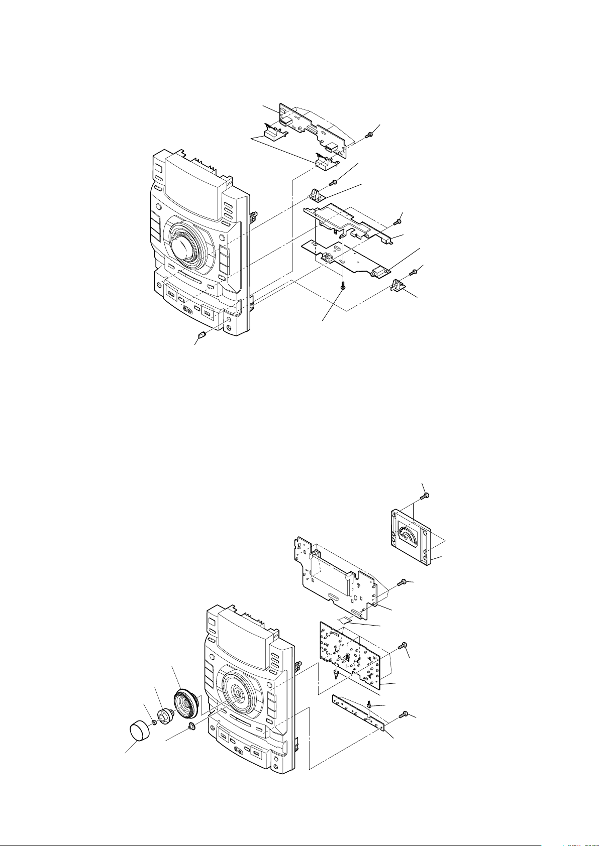
1-4. FRONT PANEL SECTION
front panel section
wire (flat type) (11 core)
(CN151)
wire (flat type) (23 core)
(CN150)
CN1501 (10P)
CN400 (13P)
By using (-) screw driver
two screws
(+BVTP 3 x 8)
four screws
(+BVTP 3 x 8)
8
HCD-GTR6/GTR6B/GTR7/GTR8/GTR8B
1-5. MIC BOARD, USB BOARD, MICRV BOARD, HEADPHONE BOARD
USB board
six screws
GROUND PLATE
(USB)
(+BVTP 2.6 (3CR))
one screw
(+BVTP 2.6 (3CR))
Headphone board
two screws
(+BVTP 2.6 (3CR))
Shield Plate (MIC)
MIC board
one screws
(+BVTP 2.6 (3CR))
RB
MICRV board
two screws
(+BVTP 2.6 (3CR))
R
knob (MIC)
1-6. DISPLAY BOARD, STR BOARD, CD SW BOARD
three screws
(+BVTP 2.6 (3CR))
four screws
(+BVTP 2.6 (3CR))
Display board
wire (flat type) (23 core)
(CN902)
meter display assy
holder (jog)
nut
knob (volume)
knob jog assy
R
gear (encoder)
RE
RT
CN903 (6P)
RH
CN901 (2P)
RI
CD SW board
RB
six screws
(+BVTP 2.6 (3CR))
STR board
RG
two screws
(+BVTP 2.6 (3CR))
9
HCD-GTR6/GTR6B/GTR7/GTR8/GTR8B
1-7. TUNER PACK
wire (flat type) (5 core)
(CN1)
tuner pack
two screws
(+BVTT 3 x 8)
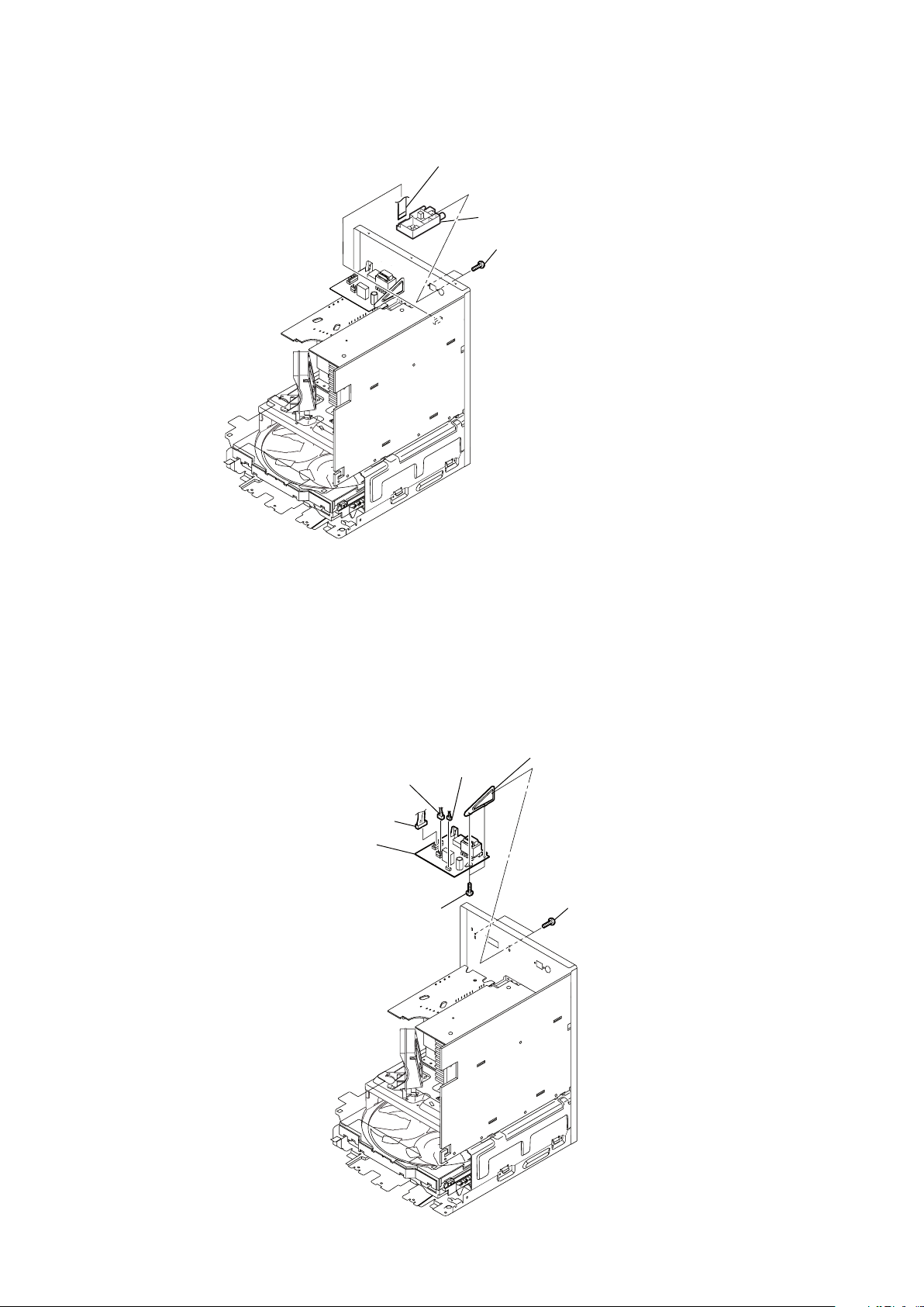
1-8. SUBTRANS BOARD
CN1200 (2P)
CN1201 (4P), CN1202 (2P)
SUBTRANS board
two screws
(+BVTP 3 x 8)
CN1203 (4P)
Bracket (Subtrans)
two screws
(+BVTP 3 x 8)
10
1-9. DC FAN, POWER TRANSFORMER (PT1250)
four screws
(+BVTT 4 x 8)
TRANS board
CN1250 (13P)
power transformer (PT1250)
CN320 (3P)
two screws
(+BVTP 3 x 8)
Fan, DC
Bracket Fan
two screws
(+BVTP 3 x 10)
HCD-GTR6/GTR6B/GTR7/GTR8/GTR8B
1-10. MAIN BOARD, FRONT BOARD SECTION
CN820 (3P)
wire (flat type) (13 core)
(CN110)
RT
Front board section
four screws
(+BVTP 3 x 8)
CN1303 (16P)
CN801 (7P)
CN1302 (11P)
RB
wire (flat type) (23 core)
(CN500)
RG
Main board
four screws
R
(+BVTP 3 x 8)
one screw
(+BVTP 3 x 8)
four screws
(+BVTP 3 x 8)
one screw
(+BVTP 3 x 8)
CN090 (9P)
RE
11
HCD-GTR6/GTR6B/GTR7/GTR8/GTR8B
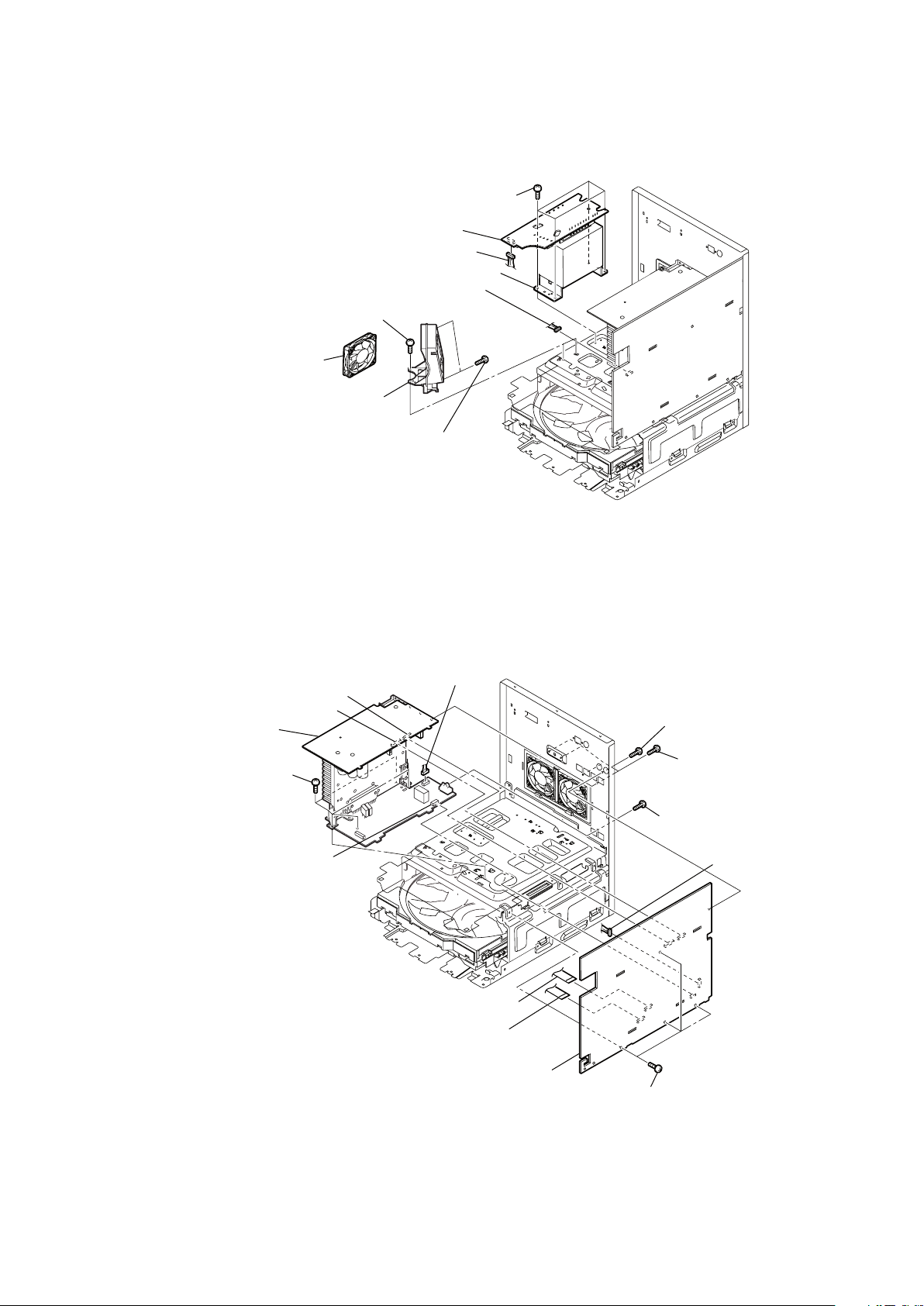
1-11. FRONT BOARD, SUBWOOFER BOARD
two screws
(+BVTP 3 x 8)
Front board
R
heat sink assy
two screws
(+BVTP 3 x 8)
Bracket (PWB)
Bracket (PC)
one screw
(+BVTP 3 x 8)
RG
SUBWOOFER board
one screw
RE
(+BVTP 3 x 8)
Bracket (PWB)
RT
two screws
(transistor)
two screws
(+BVTP 3 x 8)
two screws
RB
(transistor)
one screw
(+BVTP 3 x 8)
1-12. BACK PANEL SECTION, DC FAN
back panel section
DC fan
two screw
(+BVTP 3 x 8)
four screws
(+BVTP 3 x 8)
two screw
(+BVTP 3 x 10)
two screw
(+BVTP 3 x 10)
Cover (fan)
DC fan
12

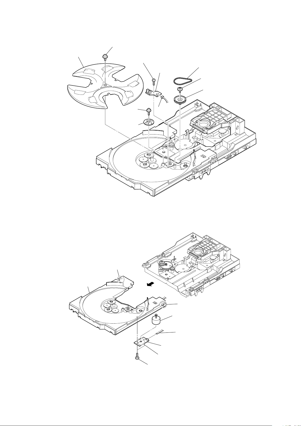
1-13. CD BLOCK SECTION
Cover Dust CDM Assy
two screws
RB
(+BVTP 3 x 8)
CD block section
Bracket (CDM Support)
three screws
(+BVTP 3 x 8)
HCD-GTR6/GTR6B/GTR7/GTR8/GTR8B
Bracket (TRANS)
two screws
(+BVTP 3 x 8)
Cover Dust (Bottom)
two screws
R
(+BVTP 3 x 8)
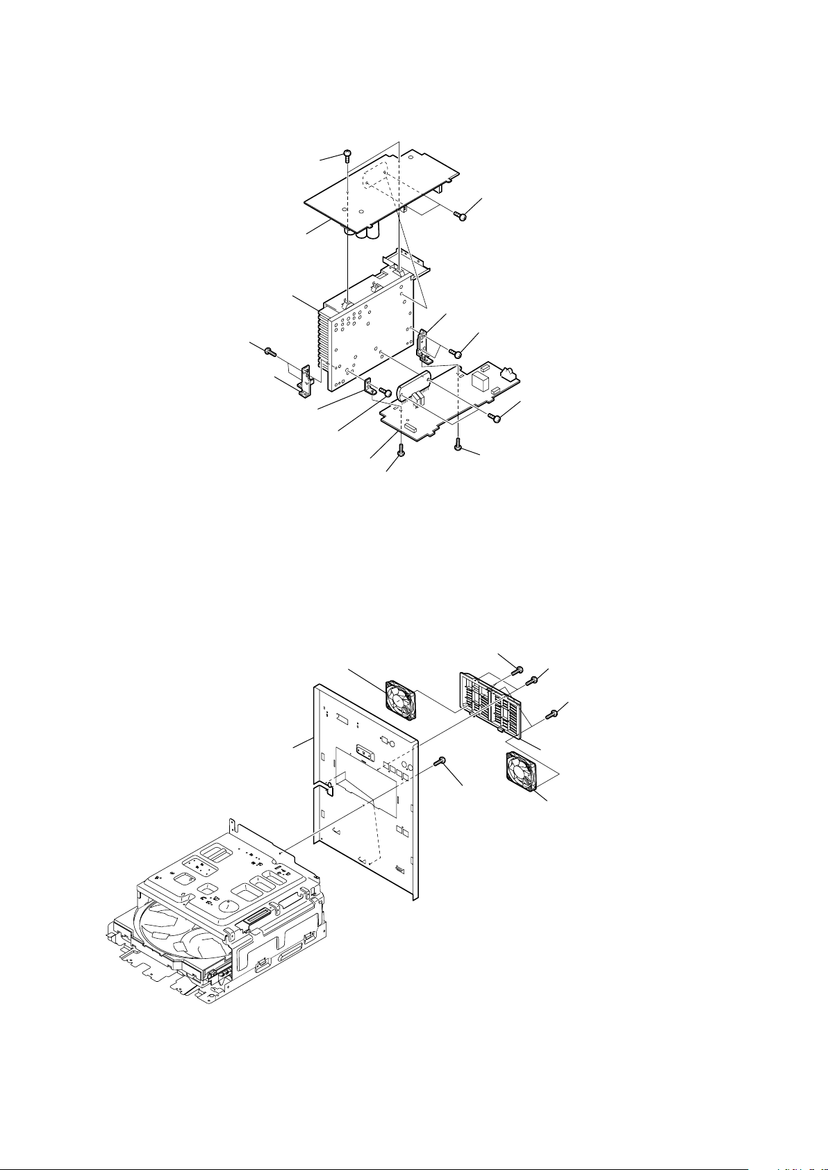
1-14. DMB19 BOARD, GTH HUB BOARD
CN201 (6P)
wire (flat type) (24 core)
(CN101)
DMB19
board
wire (flat type) (9 core)
(CN1106)
Bracket (MTK-CD)
three screws
(+BVTP 3 x 8)
(+BVTP 3 x 8)
four screws
two screws
(+BVTP 3 x 8)
Bracket (CDM Support)
one screw
(+BVTP 2.6 x 8)
one screw
(+BVTP 3 x 8)
R
two screws
(+BVTP 3 x 8)
RB
wire (flat type) (7 core)
(CN1556)
RT
GTH HUB
one screw
(+BVTP 3 x 8)
Bracket (USB HUB)
board
Sheet Dust (BU)
13

HCD-GTR6/GTR6B/GTR7/GTR8/GTR8B
1-15. DRIVER MT BOARD, SW MT BOARD
DRIVER MT board
CN704 (2P)
wire (flat type) (5 core)
(CN702)
two screws
(+BVTT (M2.6))
CN703 (4P)
one screw
(+BVTT (M2.6))
SW MT board
1-16. OPTICAL PICK-UP
floating
(+PTPWH M2.6)
insulator
insulator screw
screw
CD
assy
insulator
insulator screw
insulator
insulator screw
optical pick-up
(KHM-313CAB/C2NP)
insulator
insulator screw
14
1-17. SENSOR BOARD
t
ray
floating
(+PTPWH M2.6)
floating
(+PTPWH M2.6)
screw
screw
g
ear (geneva)
one screw
(+BTTP (M2.6))
HCD-GTR6/GTR6B/GTR7/GTR8/GTR8B
b
elt (table)
SENSOR board
floating
screw
p
ulley (table)
(+PTPWH M2.6)
CN731
(3P)
1-18. MOTOR (TB) BOARD
table
stopper
Remove the two solderings of motor.
two screws
(+BTTP (M2.6))
stopper
t
able motor assy (M741)
wire (flat type) (5 core)
(CN742)
MOTOR (TB) board
15

HCD-GTR6/GTR6B/GTR7/GTR8/GTR8B
1-19. MOTOR (LD) BOARD
Remove the two solderings of motor.
l
oading motor assy (M751)
two screws
(+BTTP (M2.6))
MOTOR (LD) board
b
elt (loading)
16

SECTION 2
TEST MODE
[GC TEST MODE]
• This mode is used to check the fl uorescent indicator tube, LEDs,
keys, VOLUME jog, OPERATION DIAL jog, model, destination
and software version.
Procedure:
1. Press [x] button, [ENTER] button and [DISC 2] button si-
multaneously.
2. All LEDs and segments in fl uorescent indicator tube are light-
ed up. All LEDs are lighted up in red color except for [
LED where the LED is lighted up in red and blue color,
[ A] LED in blue color and SUBWOOFER ON/OFF in
green color.
3. When you want to enter to the model version and destination
display mode, press [DISC 1] button. The model information
appears on the fl uorescent indicator tube.
4. Each time [DISC 1] button is pressed, the display changes to
display software version and date of the software creation.
The sequence is model destination, SC, MDK, GC, SYS, CD,
CDMA, CDMB, ST, TC, TA, TM and MTR in this order, and
returns to the model destination display.
5. Press [DISC 2] button, the key check mode is activated.
6. In the key check mode, the fl uorescent indicator tube displays
“K 0 J0 V0”.
Turn the [OPERATIONAL DIAL] clockwise; ”J” value in-
creases by one. Turn the [OPERATIONAL DIAL] counterclockwise; “J” value decreases by one. Each time a button is
pressed, “K” value increases. Press other keys on main unit
to check whether the key is detected. However, once a button
has been pressed, it is no longer taken into account.
“V” value increases in the manner of 0,1, 2, 3 ... if [VOLUME]
kno b is t urned clo ckwise, or it decrea ses in the manne r of 0 , 9,
8, 7 ... if [VOLUME] knob is turned counterclockwise.
7. When [DISC SKIP/EX-CHANGE] button is pressed after
all LEDs and segments in fl uorescent indicator tube light
up, alternate segments in fl uorescent indicator tube and LED
would light up. If you press [DISC SKIP/EX-CHANGE] button again, another half of alternate segments in fl uorescent
indicator tube and LED would light up. Press [DISC SKIP/
EX-CHANGE] button again would cause all segments will
lights off and press [DISC SKIP/EX-CHANGE] button again
all segments will lights up.
8. To release from this mode, press three buttons in the same
manner as step 1, or disconnect the power cord.
B]
HCD-GTR6/GTR6B/GTR7/GTR8/GTR8B
4. When the [VOLUME] knob is tur ned clockwise even slightly,
the sound volume increases to its maximum and a message
“VOLUME MAX” appears on the fl uorescent indicator tube.
5. When the [VOLUME] knob is tur ned counterclockwise even
slightly, the sound volume decreases to its minimum and a
message “VOLUME MIN” appears on the fl uorescent indica-
tor tube.
• Tape function (only for HCD-GTR6B/GTR8B)
1. Inserted a tape in deck. The function is changed to VIDEO
automatically when the recording is started by pressing [REC
TO TAPE] then press [ENTER] button. During recording the
ALC (Automatic Logic Control) is turned on.
2. During recording, press ALBUM - will stop the recording
and the function is changed to TAPE and rewind the tape in
Deck until the recording star t position and playback of the
tape in Deck is started.
• To release from MC Test mode
1. To release from this mode, press [POWER] button.
2. The cold reset is enforced at the same time.
[COLD RESET]
• The cold reset clears all data including preset data stored in the
RAM to initial conditions. Execute this mode when returning the
set to the customer.
Procedure:
1. Press [x] button, [ENTER] button, and [POWER] button simultaneously.
2. The fl uorescent indicator tube becomes blank for a while, and
the set is reset.
[VACS ON/OFF]
• This mode is used to switch ON and OFF the VACS (Variable
Attenuation Control System).
Procedure:
1. Press [POWER] button to turn the set ON.
2. Press [x] button and [OPTIONS] button simultaneously. The
message “VACS OFF” or “VACS ON” appears on the fl uores-
cent indicator tube.
[MC TEST MODE]
• This mode is used to check operations of the respective sections
of Amplifi er and Tape.
Procedure:
• To enter MC Test Mode
1. Press [x] button, [ENTER] button and [DISC 3] button si-
multaneously.
2. The CD number indicators fl ash on the fl uorescent indicator
tube. The function is changed to VIDEO.
• Check of Amplifi er
1. Press [EQ BAND] button repeatedly until a message “GEQ
MAX” appears on the fl uorescent indicator tube. GEQ in-
creases to its maximum.
2. Press [EQ BAND] button repeatedly until a message “GEQ
MIN” appears on the fl uorescent indicator tube. GEQ de-
creases to its minimum.
3. Press [EQ BAND] button repeatedly until a message “GEQ
FLAT” appears on the fl uorescent indicator tube. GEQ is set
to fl at.
[TUNER STEP CHANGE]
• The step interval of AM channels can be toggled between 9 KHz
and 10 KHz. This mode is not available for Saudi Arabian models.
Procedure:
1. Press [POWER] button to turn the set ON.
2. Press [TUNER/BAND] / [TU NER AM] button to select the
“A M”.
3. Press [POWER] button to turn the set OFF.
4. Press [ENTER] button and [POWER] button simultaneously.
The system will turn ON automatically. The message “AM
9K STEP” or “AM 10K STEP” appears on the fl uorescent in-
dicator tube and thus the channel step is changed.
17

HCD-GTR6/GTR6B/GTR7/GTR8/GTR8B
[CD SHIP MODE (WITH MEMORY CLEAR)]
• This mode moves the optical pick-up to the position durable to
vibration and clears all data including preset data stored in the
RAM to initial conditions. Use this mode when returning the set
to the customer after repair.
Procedure:
1. Press [POWER] button to turn the set ON.
2. Select CD function and waiting until CD no disc confi rm.
3. Press [x] button, [SOUND FLASH] button and [POWER]
button simultaneously. The set will power off automatically.
4. After the “STANDBY” blinking display fi nishes, a message
“MECHA LOCK” is displayed on the fl uorescent indicator
tube and the CD ship mode is set.
5. Then AC power OFF.
[CD SHIP MODE (WITHOUT MEMORY CLEAR)]
• This mode moves the optical pick-up to the position durable to
vibration. Use this mode when returning the set to the customer
after repair.
Procedure:
1. Press [POWER] button to turn the set ON.
2. Select CD function.
3. Press [CD] button and [POWER] button simultaneously. The
set will power off automatically.
4. After the “STANDBY” blinking display fi n i s h e s , a m e s s a g e
“MECHA LOCK” is displayed on the fl uorescent indicator
tube and the CD ship mode is set.
5. The AC power OFF.
3. The VACS Level Display, the fl uorescent indicator tube dis-
plays “VATB F APC”. “V” represent VACS , A represent
VACS level which is triggered by signal level, “T” represent
Thermal VACS NEO, B represent VACS level which is triggered by temperature, “F” represent FAN is triggered by
software to turn in to high speed, “AP” represent APVACS
(Abuse Protection VACS) and “C” represent APVACS level
which is triggered.
[METER AGING TEST MODE]
• This mode use in factory to perform the non-stop aging mode for
meter device.
Procedure:
1. Press [POWER] button to turn on the system.
2. Press [EQ BAND/MEMORY] button and [METER MODE]
button simultaneously.
[ERROR MESSAGE]
1. METER ERROR CODE CHECK
• This mode is used to check the number of trigger for Meter Pointer
to initial switch and end switch. The switches will trigger during
meter initialize in AC supply on condition.
Procedure:
1. Press [POWER] button to turn on the system.
2. Press [x] button, [EQ BAND/MEMORY] button and [METER MODE] button simultaneously.
[CD TRAY LOCK MODE / DISC THEFT
PREVENTION]
• This mode let you lock the disc tray. When this mode is activated,
the disc tray will not open when [OPEN/CLOSE] button or [EXCHANGE] button is pressed. The message “LOCKED” will be
displayed on the fl uorescent indicator tube.
Procedure:
1. Press [POWER] button to turn the set ON.
2. Select CD function.
3. Press [x] button and [OPEN/CLOSE] button simultaneously
and hold down until “LOCKED” or “UNLOCKED” displayed on the fl uorescent indicator tube (around 5 seconds).
[TCM OFFLINE MODE]
(only for HCD-GTR6B/GTR8B)
• This mode prevents set from power off automatically when TCM
is not connected. Therefore, measurements can be done even when
TCM is not connected.
Procedure:
1. When the system in turned off, press [EQ BAND/MEMORY]
button, [STOP] button and [POWER] button simultaneously.
The set will power on automatically.
2. The message “TCM OFFLINE” will be displayed on the fl uo-
rescent indicator tube.
The Meter Er ror Code will appear on the fl uorescent indicator
tube displays
• Display
Display on fl uorescent indicator tube,
IxxxxxMyyyyy
Ixxxxx = total number of Initial Switch touch by Meter
pointer. The Initial Switch will touch twice during meter
initialized process.
Myyyyy = total number of End Switch touch by Meter
pointer. The End Switch will touch one times during meter
initialized process.
[VACS DISPLAY]
• This mode is used to check the VACS level.
Procedure:
1. Press [POWER] button to turn on the system.
2. Press [x] button, [SOUND FLASH] button and [DISC SKIP/
EX-CHANGE] button simultaneously.
18

SECTION 3
MECHANICAL ADJUSTMENTS
(only for HCD-GTR6B/GTR8B)
Precaution
1. Clean the following parts with a denatured alcohol-moistened
swab:
record/playback heads pinch rollers
erase head rubber belts
capstan idlers
2. Demagnetize the record/playback head with a head demagnetizer.
3. Do not use a magnetized screwdriver for the adjustments.
4. After the adjustments, apply suitable locking compound to the
parts adjusted.
5. The adjustments should be performed with the rated power
supply voltage unless otherwise noted.
Torque Measurement
Mode Torque meter Meter reading
2.9m N • m to 6.9m N • m
FWD CQ-102C 30 to 70 g • cm
(0.42 – 0.97 oz • inch)
FWD 0.15m N • m to 0.59m N • m
back tension CQ-102C 2 to 6 g • cm
(0.03 – 0.08 oz • inch)
2.9m N • m to 6.9m N • m
REV CQ-102RC 30 to 70 g • cm
(0.42 – 0.97 oz • inch)
0.15m N • m to 0.59m N • m
REV
CQ-102RC 2 to 6 g • cm
back tension
4.8m N • m to 16.7m N • m
FF/REW CQ-201B 49 to 170 g • cm
(0.68 – 2.36 oz • inch)
(0.03 – 0.08 oz • inch)
HCD-GTR6/GTR6B/GTR7/GTR8/GTR8B
19

HCD-GTR6/GTR6B/GTR7/GTR8/GTR8B
SECTION 4
ELECTRICAL ADJUSTMENTS
TUNER SECTION 0 dB = 1 µV
[FM Tune Level Check]
FM signal generator
SET
Procedure:
1. Turn the power on.
2. Input the following signal from Signal Generator to FM antenna input directly.
* Carrier Freq : A = 87.5 MHz, B = 98 MHz, C = 108 MHz
Deviation : 75 kHz
Modulation : 1 kHz
ANT input : 35 dBu (EMF)
Note: Please use 75 ohm “coaxial cable” to connect SG and the set. You
cannot use video cable for checking.
Please use SG whose output impedance is 75 ohm.
3. Set to FM tuner function and tune A, B and C signals.
4. Confi rm “TUNED” is lit on the display for A, B and C sig-
nals.
The mark of “TUNED” means “The selected station signal is
received in good condition.”
OUT (75 7)
DECK SECTION 0 dB = 0.775 V
(only for HCD-GTR6B/GTR8B)
1. Demagnetize the record/playback head with a head
demagnetizer.
2. Do not use a magnetized screwdriver for the adjustments.
3. After the adjustments, apply suitable locking compound to the
parts adjust.
4. The adjustments should be performed with the rated power
supply voltage unless otherwise noted.
5. The adjustments should be performed in the order given in this
service manual. (As a general rule, playback circuit adjustment should be completed before performing recording circuit
adjustment.)
6. The adjustments should be performed for both L-CH and RCH.
7. Switches and controls should be set as follows unless otherwise
specifi ed.
• Test Tape
Tape Signal Used for
P-4-A100 10 kHz, –10 dB Azimuth Adjustment
[RECORD/PLAYBACK HEAD AZIMUTH
ADJUST-MENT]
Note: Perform this adjustments for Single deck
Procedure:
1. Mode: Playback
test tape
P-4-A100
(10 kHz, –10 dB)
(L-CH & R-CH)
set
level meter
+
–
2. Turn the adjustment screw and check output peaks. If the peaks
do not match for L-CH and R-CH, turn the adjustment screw
so that outputs match within 1dB of peak.
output
level
within
1dB
L-CH
peak
R-CH
peak
within
1dB
screw
position
L-CH
peak
screw
position
R-CH
peak
20

3. Mode: Playback
test tape
P-4-A100
(10 kHz, –10 dB)
L-CH
R-CH
oscilloscope
L
R
waveform of oscilloscope
HCD-GTR6/GTR6B/GTR7/GTR8/GTR8B
H
V
in phase
45o 90o 135o 180o
good
wrong
4. After the adjustments, apply suitable locking compound to
the parts adjusted.
Adjustment Location: Playback Head (Deck).
Reverse Rorward
21
HCD-GTR6/GTR6B/GTR7/GTR8/GTR8B
SECTION 5
DIAGRAMS
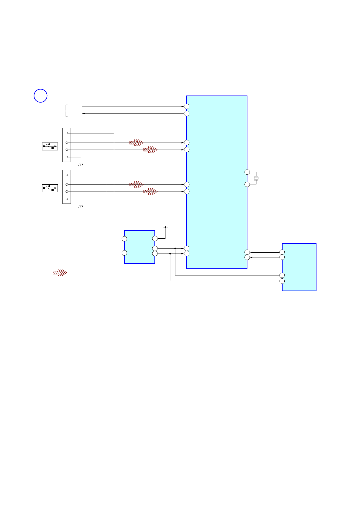
5-1. BLOCK DIAGRAM — USB SECTION —
A
1
4
USB_DP
USB_DM
VBUS_B
D- B
D+ B
GND
RF/SERVO
SECTION
(Page 23)
CN1000
(USB)
31
30
3
4
USBUP_DP
USBUP_DM
USBDN2_DM
USBDN2_DP
IC1501
USB CONTROLLER
CN1001
(USB)
Signal Path
XTAL2
RESET_N
VBUS_DET
33
X1500
24MHz
32
26 21
27
SYSTEM CONTROL
USB_HUB_RESET
22
HUB_VBUS_DET
18
USB-OC1
USB-OC2
19
IC500 (4/6)
VBUS_A
1
D- A
D+ A
GND
4
IC1500
: USB
SINGLE-SUPPLY
DUAL COMPARATOR
+IN2
5
+IN1
3
VCC
OUT1
OUT2
M+9V
8
1
7
1
2
13
17
USBDN1_DM
USBDN1_DP
OSC1_N
OSC2_N
XTAL1/CLKIN
22

23 23
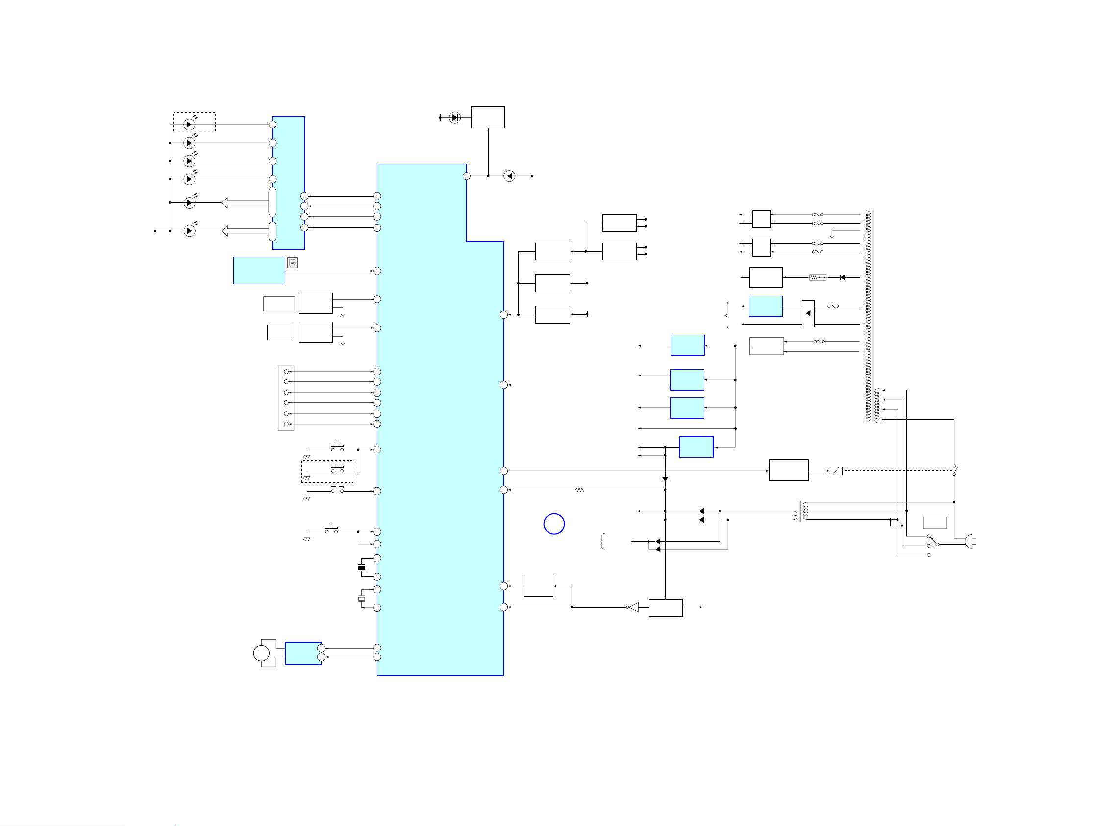
HCD-GTR6/GTR6B/GTR7/GTR8/GTR8B
HCD-GTR6/GTR6B/GTR7/GTR8/GTR8B
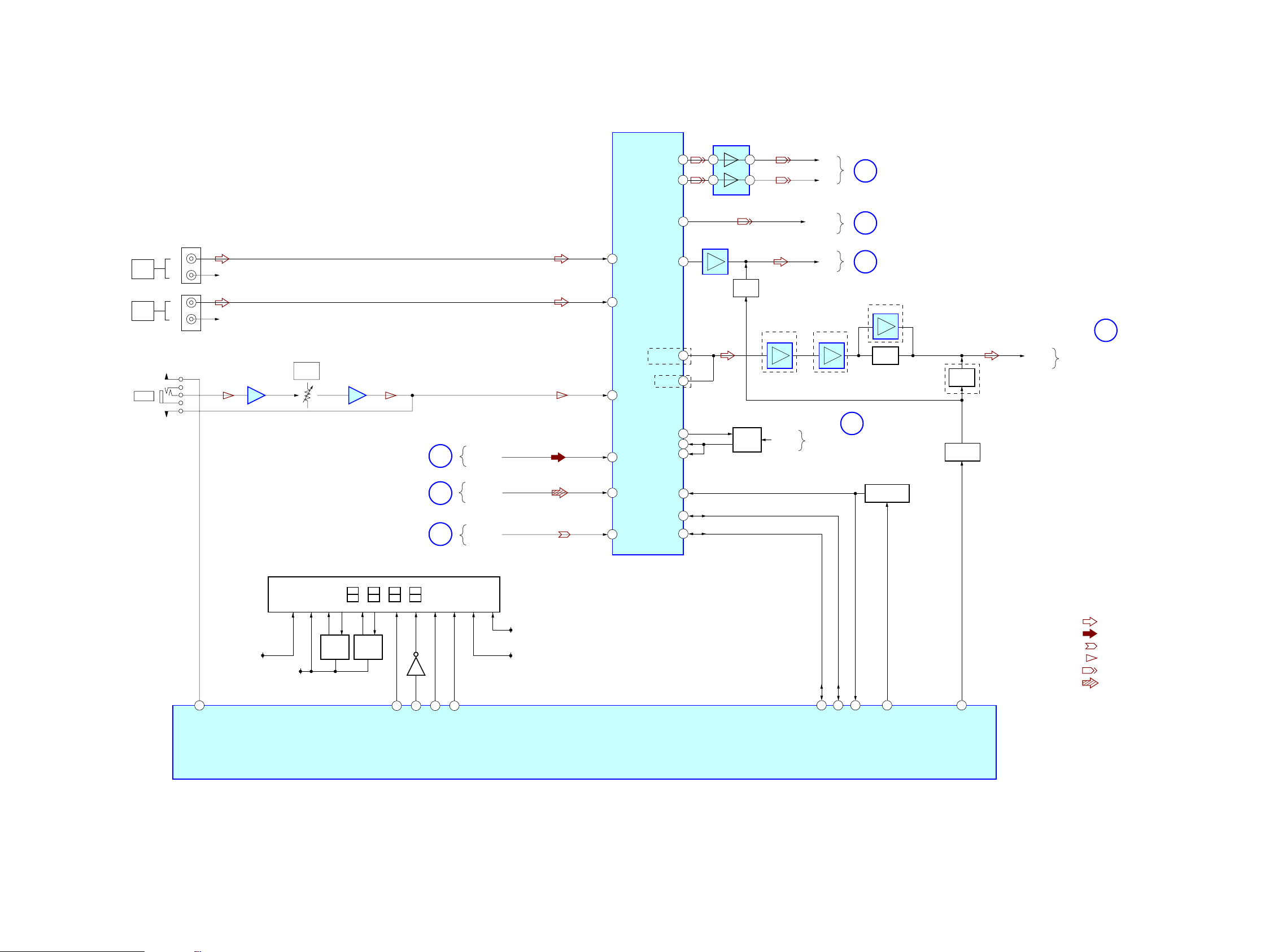
5-2. BLOCK DIAGRAM — RF/SERVO SECTION —
DETECTOR
125
2
3
4
5
19
18
RFIP
OPOUT
RF_C
RF_B
RF_A
RF_D
RF_E
RF_F
LD01
MDI2
LD02
MSW
MDI1
CD RF AMP,
FOCUS/TRACKING ERROR AMP
CD SYSTEM PROCESSOR
DIGITAL SERVO PROCESSOR
IC101
OPTICAL PICK-UP
BLOCK
(KHM-313CAB)
2AXIS
DEVICE
FOCUS/
TRACKING
COIL
17
16
18
15
36 48
43
12
9
37 1
Q102 (2/2)
AUTOMATIC POWER
CONTROL (FOR DVD)
Q102 (1/2)
AUTOMATIC POWER
CONTROL (FOR CD)
LASER
DIODE
(FOR CD)
LASER
DIODE
(FOR DVD)
FOCUS COIL
DRIVE
42
41
BUFFER
35 3
34 4
TRACKING COIL
DRIVE
32
31
21
25
20
24
13
SLED MOTOR
DRIVE
FOCUS/TRACKING COIL DRIVER,
SPINDLE, SLED MOTOR DRIVER
IC201
27
28
SPINDLE MOTOR
DRIVE
MM
M1
(SPINDLE)
S1
(LIMIT)
46
47
FMO
FOO
DMO
TRO
VREFO
127
IOPMON
FOO
RF
A
B
C
D
E+H
E+G
CD LD
VC
PD
VR650
VR780
DVD LD
FCS+
MSW
FCS–
TRK+
REG02
REG01
TRK–
SP+
SP–
SL+
SL–
NC
NC
VREFO
V2O
12
30
29
SLED MOTOR
DRIVE
MM
M2
(SLED)
23
BUFFER
21
20
22
45
19
42
40
SYSTEM
CONTROLLER
IC500 (1/6)
64M RAM
IC104
91
TXD
40
IFSCK
MTK_CLK
33
TXD
CN105
RXD
RFMON
89
RXD
43
PRST
37
DF_D0
38
SF_CL
39
SF_CK
36
SF_CS
MTK-RESET
23
88
IFCS MTK_XIFCS
24
35
IFSDI
87
IFBSY MTK_BUSY
25
MTK SIO
47
78
BA0
BA0
20
80
BA1
BA1
21
55
DQSM
LDQM
15
75
RWE
WE
16
76
CAS0
CAS
17
77
RAS0
RAS
18
66
RCLK
CLK
38
65
DQM1
UDQM
39
TRO
10
13
FMO
IOP
IOPMON
DMO
107
MUTE123
22
MUTE4
94
GP1O
128
SPFG
MUTE123
MUTE
TSD M
SPFG
108
LIMSW
Q101
Q103
7
6
(FOR TEST)
1
2
6
• Signal Path
: CD PLAY
: REC
126
41
IFSOD
MTK_SOD
48
FLASH
MEMORY
IC102
1.2V REG
IC 111
1.2V REG
IC107
SI
2
SCK
5
CS
6
SO
1
STEREO
CONVERTER
A/D
IC4601
114
GPIO
GPIO
GPIO
GPIO19
SCKI
6
119
LRCK
7
115
GPIO
120
BCK
8
106
DOUT
VINL
9
CONVERTER
D/A
IC4602
MCLK
AOUT-L
AOUT-R
4
LRCK
3
SCLK
2
SDATA
1
13
L IN
8
LOUT
5
ROUT
67
69
I
81
I
I
83
85
RA0
USB_DP
27
USB_DM
USB_DP
USB_DM
28
74
I
RA11
45
I
RD0
49
51
I
53
56
I
59
61
I
64
I
RD15
A0
I
A3,
A10
A4
I
A9,
A11
22
I
26
29
I
35
QG0,
DQ1
I
DQ15
2,4,5,7,8,10,11,13,42,
45,47,48,50,51,53,55
R-CH is omitted due to same as L-CH.
DVDD3.3V
DVDD5V
86
J
MAIN
SECTION
(Page 25)
B
MAIN
SECTION
(Page 25)
A
USB
SECTION
(Page 22)

2424
HCD-GTR6/GTR6B/GTR7/GTR8/GTR8B
HCD-GTR6/GTR6B/GTR7/GTR8/GTR8B
5-3. BLOCK DIAGRAM — TAPE/TUNER SECTION —
ST-L
MAIN
REC-OUT-L
MAIN
TAPE
MECHANISM
BLOCK
ST-R
TU901
FM/AM TUNER UNIT
ANTENNA
GTR6B/8B
GTR6B/8B
ST-L
FM ANT
AM ANT
AM ANT
ST-R
ST-DIN
ST-DOUT
ST-CLK
ST-CE
FM 75
COAXIAL
CAP M+
BTRGM+
BHALF
B SHUT
CAPM-+
B-HALF
B-SHUT
REC BIAS
REC-MUTE
AM
ST-DIN/UC-OUT
ST-DOUT/UC-DIN
ST-CLK
ST-CE
72
75
46 3
80
81
78
E-1
40
E-2
42
E-3
43
65
60
63
TUNED
ST-TUNED
58
61
SYSTEM CONTROL
(TAPE MECHANISM CONTROL)
IC500 (2/6)
TAPE_PB-L
C
MAIN
DECK
BIAS OSC
Q300
REC
MUTE
OP-AMP
R-CH
Q456
IC451
REC EQ
IC450
Q406
Q402, Q404
Q407
R-CH
M+9V
REC/PB
HEAD
ERASE
HEAD
Q301,302
T300
L - CH
R - CH
REC(FWD)
R-CH is omitted due to same as L-CH.
A TRIGGER DRIVE
Q001,003
CAPSTAN MOTOR DRIVE
Q002,004
4
1
2
TABLE ADDRESS SENSOR
IC731
TBL MOTOR DRIVER
IC712
M+9V
Q731
RE701
ROTARY ENCODER
DISC TRAY
ADDRESS DETECT
S751
OPEN/CLOSE
DETECT
TBL SENSE
OPENSW
46
MOTOR
DRIVE
M741
(TABLE)
M
TM F
FIN
RIN
39
TM R
38
7
9
OUT2
OUT1
2
4
MUTE SW
Q409,410
B-TRIG
79
TC-RELAY
82
RELAY SW
Q408
+9V
: TAPE PLAY
: TUNER
: RECORD
Signal Path
D
E
SECTION
(Page 25)
(Page 25)
(Page 25)
SECTION
SECTION
25 25
HCD-GTR6/GTR6B/GTR7/GTR8/GTR8B
HCD-GTR6/GTR6B/GTR7/GTR8/GTR8B
5-4. BLOCK DIAGRAM — MAIN SECTION —
J1001
J020
RCH
L
R
AUDIO
IN
INPUT SELECT SWITCH
IC400
MIC AMP
IC1000
(1/2)
MIC AMP
IC1000
(2/2)
RV1001
MIC
LEVEL
MIC-DET
AUDIO IC CLOCK
AUDIO IC DATA
LINE MUTE
SYSTEM CONTROL
IC500 (3/6)
9SA2
CD-L
42
76
52 53 51
METER LEVEL
71
VAC-IN
70
RCH
L
R
VIDEO
IN
DBFB
SWITCH
Q128
ST-L
TAPE_ PB-L
X
TAPE/TUNER
TAPE/TUNER
E
AMP/SUBWOOFER
RF/SERVO
REC OUT L
TAPE/TUNER
D
AMP/SUBWOOFER
AMP/SUBWOOFER
DBFB F/B
R-IN
L-IN
45
TAPE-L
43
ST-L
41
VIDEO-L
44
PC-L
46
MIC
FL-IN
26
OUTL
36
RECBL
25
AGCOUTL
23
SWOUT
27
BB2L
48
REFOUT
28
BB1L
DATA
21
22
CLOCK
RECAR
RECAL
SW OUT
MUTE
Q270
MUTE
Q245
Q721
SWITCH
LINE MUTE
Q290
Q210
J1004
MIC
METER LEVEL
AMP
IC252
GTR7
GTR8/8B
GTR8/8B
IC253 IC254
IC730
8
CIG-CLK
GIG-BK
CIG-DATA
GIG-LATCH
VF+
VF-
D+3.3V
+VG
35 282637
15
3
1113
ND900
1012484546 479
Q901
7
5
3
37
6
1
IC251
USB RECORD
PREAMP
: AUDIO
: TAPE PLAY
: MIC
: REC
: CD PLAY
: TUNER
Signal Path
R-CH is omitted due to same as L-CH.
CD LCH
RF/SERVO
Q903Q902
SWITCH SWITCH
GTR7/8/8B
GTR7/8/8B
XB
XC
I
J
F
G
SECTION
(Page 23)
(Page 24)
(Page 26)
(Page 26)
(Page 26)
SECTION
SECTION
SECTION
(Page 24)
(Page 24)
(Page 23)
SECTION
SECTION
SECTION
SECTION
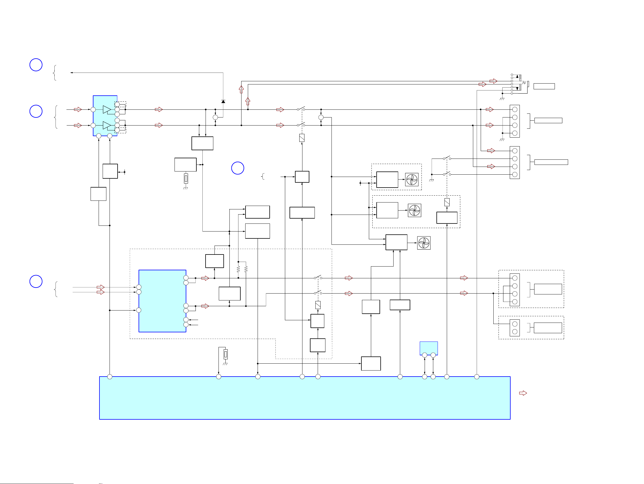
2626
HCD-GTR6/GTR6B/GTR7/GTR8/GTR8B
HCD-GTR6/GTR6B/GTR7/GTR8/GTR8B
5-5. BLOCK DIAGRAM — AMP/SUBWOOFER SECTION —
IC1301: GTR7/8/8B
IC1300: GTR6/6B
MUTING
Q1312
-1314
FR-IN
DBFB F/B
FL-IN
31
STK MUTE
1216
OVERLOAD
DETECT
Q1303,1308
+ +
33 77
LINK RELAY
97
EEPROM_DATA
95
5 6
EEPROM_CLOCK
HP DET
AC-CUT
Q1301
FRONT REPLAY
Q1302
+VL
-VL
IN2
ST BY
+RE1
-RE1
+RE2
-RE2
+VCC
-VCC
+
-
-
+
FRONT SPEAKER
SUB WOOFER
OUT
L
R
HEADPHONE
J1005
RY1301
RY862
+
-
-
+
L
R
FAN
DRIVE
Q031-Q034
DRIVE
TH1301
THERMAL
DETECT
Q1309,Q1310
67
THERMAL VACS
TB801
JK1301
D104
18
11
10
22
9
14
8
SIGNAL PATH
POWER AMP
32
PROTECTOR
50
FR RELAY
56
FAN ON
G
MAIN
TH1300
11
4
5
6
7
3
2
13
SUBWOOFER POWER AMP
IC800
SYSTEM CONTROL
IC500 (5/6)
PROTECTOR
Q1305,Q1307
DC DETECT
Q1304,Q1306
OVERLOAD
DETECT
Q850
Q788
RELAY
DRIVE
Q789
OVERLOAD
DETECT
Q800
RY1300
EXCEPT MX
GTR7/8/8B
HI SPEED
SWITCH
Q035
PROTECTOR
SWITCH
Q532
+
-
-
+
SURROUND SPEAKER
L
R
JK1300
RELAY DRIVE
Q1300
45
SW-RELAY
R-CH is omitted due to same as L-CH.
EEPROM
IC675
FAN DETACT
Q030
GTR8 / GTR8B
SUB WOOFER
OUT
+
-
TB802
GTR7
GTR7/8/8B
GTR7/8
GTR7/8
UNREG
+VH
STANDBY
Q1315,
Q1316
: AUDIO
IN1
SW-R IN
SW-L IN
AC DETACT
15
M891
DC FAN
DC FAN
M892
21
AC CUT
DETECT
FAN
DRIVE
Q821,824,825
Q036,038,039
M893
DC FAN
FAN
F
MAIN
I
MAIN
SECTION
SECTION
SECTION
(Page 25)
(Page 25)
(Page 25)
H
DISPLAY/POWER
SECTION
(Page 27)
27 27
HCD-GTR6/GTR6B/GTR7/GTR8/GTR8B
HCD-GTR6/GTR6B/GTR7/GTR8/GTR8B
5-6. BLOCK DIAGRAM — DISPLAY/POWER SECTION —
M
MOTOR
DRIVE
IC701
MOTOR(LD)
M751
9
7
+5V
3.3V
94 MASTER VOL
STK MUTE
LMR
MASTER
VOLUME
88 ADKEY1
90 ADKEY2
73 POWER KEY
S945,S950-54,
S908-06
4 SIRCS
X514
5MHz
15 X-IN
13 X-OUT
X510
32.768kHz
10 XC-IN
11
36
34
XC-OUT
SYSTEM CONTROL
IC500 (6/6)
68STBY-RELAY
12RESET
20AC-CUT
D1203
RECT
D1314
RECT
D1313
+VL
F1261
VL
VL
VH
VH
VP
VF
VF
GND
F1251
F1241
F1231
R1271
-VL
+VH
-VH
+33V
REGULATOR
Q1250
POWER ON/OFF
RELAY DRIVE
Q1200
+ VG
(+32V)
D1252
RECT
VF+
VF-
ND900
VACUUM
FRUORESCENT
DISPLAY
RY1200
PT1250
POWER
TRANSFORMER
RESET
SWITCH
Q005
REMOTE CONTROL
SIGNAL RECEIVER
IC900
EVER +10V
AC-CUT
DETACT
93 OP DIAL
ENCODER
ROTARY
ROTARY
ENCODER
OPERATION
DIAL
69OVER_VOLTAGE_DET
RECT
D600
M +9V
LED +9V
ST+9V
3
27USB_OE
55
MTK_POWER_CONTROL
+3.3V
+9V
+9V
+AVDD5V
+9V
+DVDD5V
AC3
AC3
F1271
F1281
UNREG/UNREGULATE
S936
S935
+9V REG
IC200
+9V REG
IC055
+4V REG
IC676
+5V REG
IC065
+3.3V REG
IC095
S916,S918,S920,S922,
S924,S926,S928,S930,
S932,S934,S936,S938,
S940-42
89 ADKEY0
34
31
S915,S917,S919,S921,
S923,S925,S927,S929,S931,
CLK1
RXD1
TXD1
RTS1
CN VSS
RESET
GTR7/8/8B
CN040
(FOR PROGRAMMING)
LINK RELAY
PROTECTOR
32
33
CNVss
RESET
12
9
D901
D900
LED
SWITCH
Q900
LED +9V
EVER 3.3V
STBY LED
2 LED DRIVER-DATA
LED DRIVER-CLOCK
7
1
41
LED DRIVER-LATCH
LED DRIVER-OE
4
8
6
5
1,
2,
21
|
24
15
|
20
LATCH
IC901
LED +9V
D923-928
D922,
D929-931
+3.3V REG
Q007-009
D1201
D010
D1202
EVER 3.3V
Q006
SUB POWER
TRANSFORMER
PT1200
8
6
D1253-1256
S1200
AC IN
230-240V
220V
120V/127V
VOLTAGE
SELECTOR
11
12
13
D1022
D1021
D1020
14
D919
GTR7/8/8B
Q712,Q717
RECT
RECT
Q713,Q714
RECT
Q720
RECT
Q719
RECT
Q696,Q718
AMP/SUFWOOFER
H
S933,S937
SECTION
(Page 26)
2828
HCD-GTR6/GTR6B/GTR7/GTR8/GTR8B
HCD-GTR6/GTR6B/GTR7/GTR8/GTR8B
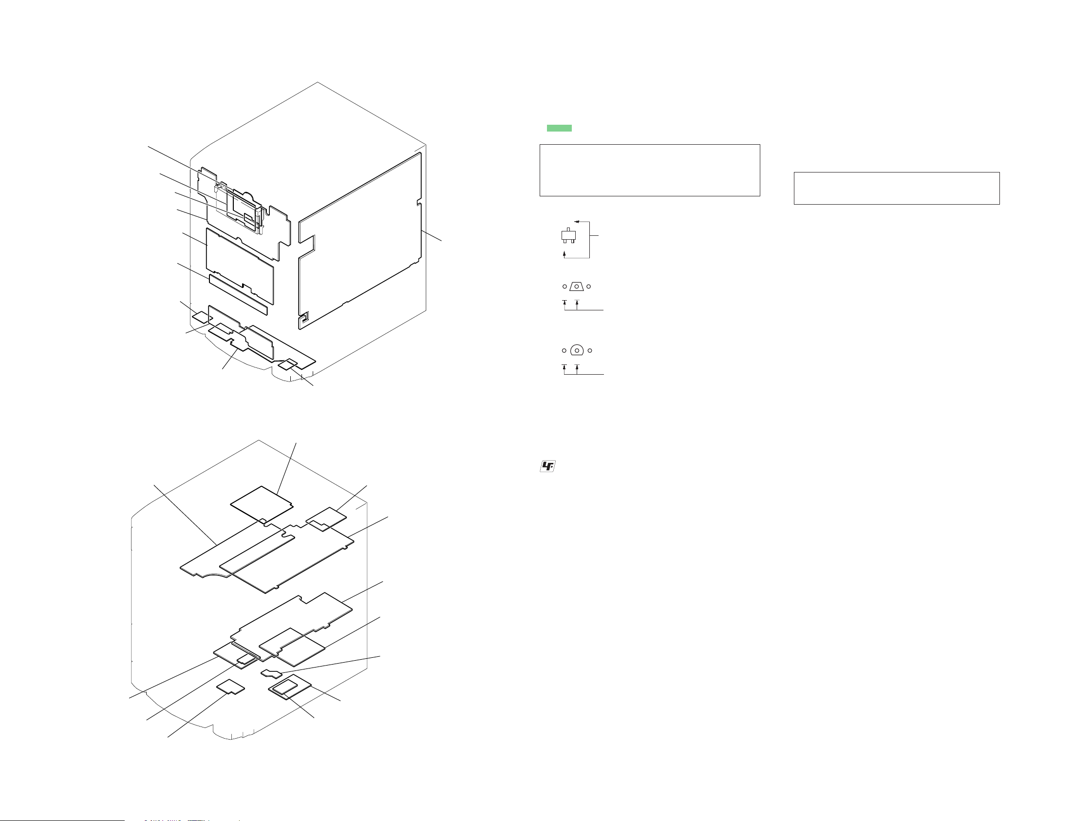
5-7. CIRCUIT BOARDS LOCATION
Motor Drive board
included in METER DISPLAY ASSY
MAIN board
HEAD PHONE board
MIC CD board
CD SW board
STR board
Display board
SW board
included in METER DISPLAY ASSY
LED board
included in METER DISPLAY ASSY
USB CD board
MIC RV board
• Note For Printed Wiring Boards And Schematic Diagrams
Note on Printed Wiring Board:
• X : parts extracted from the component side.
• Y : parts extracted from the conductor side.
• : Pattern from the side which enables seeing.
(The other layer’s patterns are not indicated.)
Caution:
Pattern face side: Parts on the pattern face side seen from
(Conductor Side) the pattern face are indicated.
Parts face side: Parts on the parts face side seen from
(Component Side) the parts face are indicated.
• Indication of transistor.
• A : B+ Line.
• B : B– Line.
• Voltage and waveforms are dc with respect to ground
under no-signal (detuned) conditions.
• BD93 and Driver sections.
no mark : CD PLAY
• Except BD93 and Driver sections.
no mark : FM
( ) : CD PLAY
< > : TAPE PLAY
[ ] : TAPE REC
∗ : Impossible to measure
• Voltages are taken with a VOM (Input impedance 10
MΩ).
Voltage variations may be noted due to normal production
tolerances.
• Waveforms are taken with a oscilloscope.
Voltage variations may be noted due to normal production
tolerances.
• Circled numbers refer to waveforms.
• Signal path.
F : AUDIO
f : TUNER
E : TAPE PLAY
G : TAPE REC
N : MIC
J : CD PLAY
c : DIGITAL
I : USB
• Abbreviation
E2 : 120V AC area in E model
E3 : 240V AC area in E model
E51 : Chilean and Peruvian model
AR : Argentina model
AUS : Australian model
MX : Mexican model
Note: The components identifi ed by mark 0 or dotted line
with mark 0 are critical for safety.
Replace only with part number specifi ed.
UNLEADED SOLDER
Boards requiring use of unleaded solder are printed with the lead
free mark (LF) indicating the solder contains no lead.
(Caution: Some printed circuit boards may not come printed with
the lead free mark due to their particular size)
: LEAD FREE MARK
Unleaded solder has the following characteristics.
• Unleaded solder melts at a temperature about 40 °C higher than
ordinary solder.
Ordinary soldering irons can be used but the iron tip has to be
applied to the solder joint for a slightly longer time.
Soldering irons using a temperature regulator should be set to
about 350 °C.
Caution: The printed pattern (copper foil) may peel away if the
heated tip is applied for too long, so be careful!
• Strong viscosity
Unleaded solder is more viscous (sticky, less prone to fl ow) than
ordinary solder so use caution not to let solder bridges occur such
as on IC pins, etc.
• Usable with ordinary solder
It is best to use only unleaded solder but unleaded solder may also
be added to ordinary solder.
Note on Schematic Diagram:
• All capacitors are in µF unless otherwise noted. (p: pF)
50 WV or less are not indicated except for electrolytics
and tantalums.
• All resistors are in Ω and 1/
4
W or less unless otherwise
specifi ed.
• 2 : nonfl ammable resistor.
• C : panel designation.
• Abbreviation
MX : Mexican model
TRANS board
SUBTRANS board
TUNER PACK
FRONT board
SUBWOOFER board
DMB19 board
C
Q
B
B
B
These are omitted.
E
Q
CE
These are omitted.
Q
CE
These are omitted.
HUB board
SW board
MOTOR (LD) board
MOTOR (TB) board
SENSOR board
DRIVER board
 Loading...