

Sony HCD-GPX33, HCD-GPX55, HCD-GPX77, HCD-GPX88 Schematic
SERVICE MANUAL
Sony Corporation
Published by Sony EMCS (Malaysia) PG Tec
HCD-GPX33/GPX55/GPX77/
GPX88
SPECIFICATIONS
9-890-622-01
2013C80-1
©
2013.03
Ver. 1.0 2013.03
• HCD-GPX33 is the amplifi er, USB, CD player,
Bluetooth, NFC and tuner section in MHC-GPX33.
• HCD-GPX55 is the amplifi er, USB, CD player,
Bluetooth, NFC and tuner section in MHC-GPX55.
• HCD-GPX77 is the amplifi er, USB, CD player,
Bluetooth, NFC and tuner section in MHC-GPX77.
• HCD-GPX88 is the amplifi er, USB, CD player,
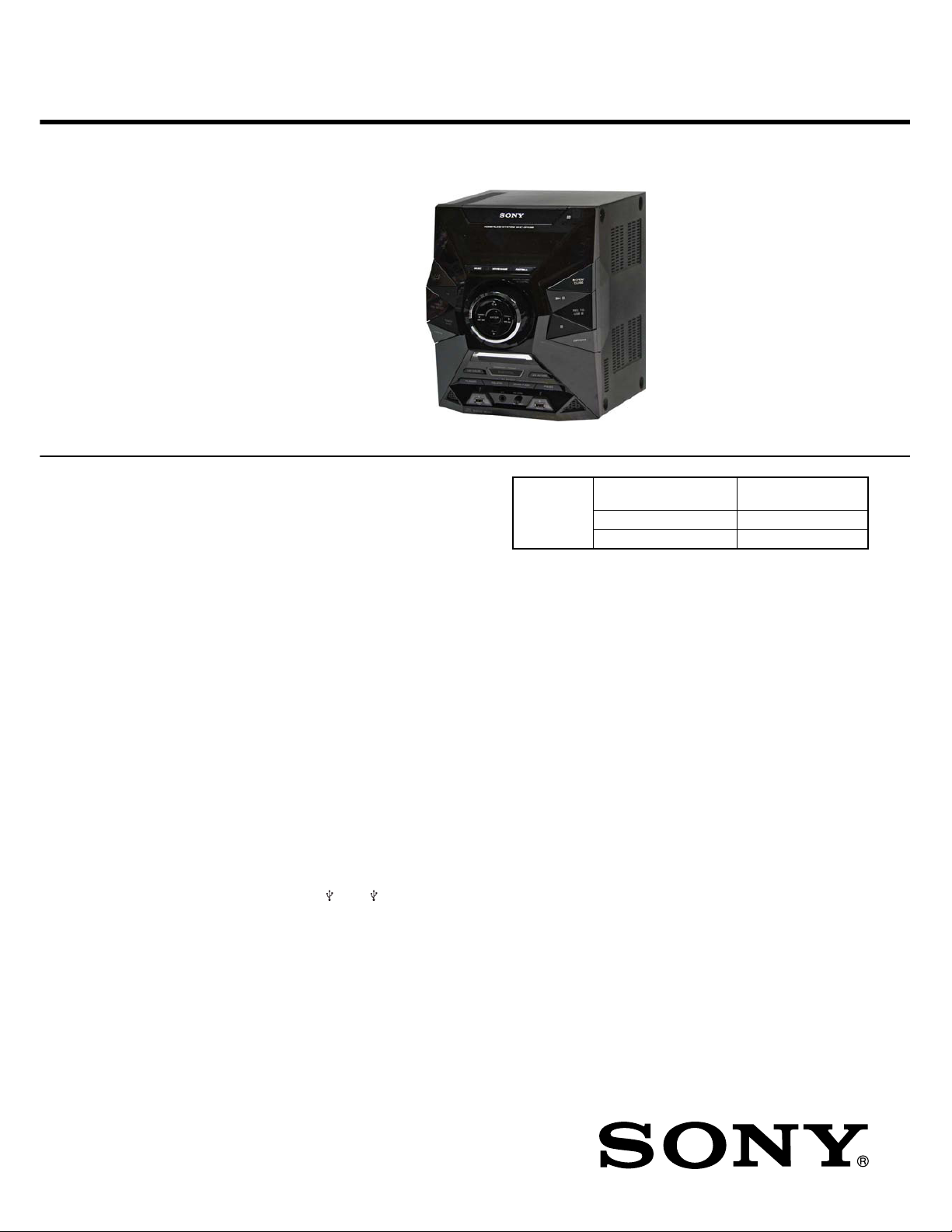
Bluetooth, NFC and tuner section in MHC-GPX88. Photo: HCD-GPX88
“WALKMAN” and “WALKMAN” logo are registered trademarks of Sony Corporation.
MPEG Layer-3 audio coding technology and patents licensed from Fraunhofer IIS and Thomson.
Windows Media is either a registered trademark or trademark of Microsoft Corporation in the United States
and/or other countries.
This product is protected by certain intellectual property rights of Microsoft Corporation. Use or distribution
of such technology outside of this product is prohibited without a license from Microsoft or an authorized
Microsoft subsidiary.
The Bluetooth
®
word mark and logos are registered trademarks owned by Bluetooth SIG, Inc. and any use
of such marks by Sony Corporation is under license. Other trademarks and trade names are those of their
respective owners.
The N Mark is a trademark or registered trademark of NFC Forum, Inc. in the United States and in other
countries.
Android is a trademark of Google Inc.
All other trademarks and registered trademarks are of their respective holders. In this manual, ™ and ® marks
are not specified.
CD Section
Model Name Using
Similar Mechanism
NEW
CD Mechanism Type CDM90-DVBU202//M
Optical Pick-up Name CMS-S76RFS7G
COMPACT DISC RECEIVER
US Model
HCD-GPX55/GPX77
E Model
HCD-GPX33/GPX55/GPX77/GPX88
Australian Model
HCD-GPX77
Mexican Model
HCD-GPX33/GPX77/GPX88
Saudi Arabia Model
HCD-GPX33/GPX77
AUDIO POWER SPECIFICATIONS
POWER OUTPUT AND TOTAL HARMONIC
DISTORTION:
(USA model only)
With 4 ohm loads, both channels driven, from
120 – 10,000 Hz; rated 130 watts per channel
minimum RMS power, with no more than
0.7% total harmonic distortion from 250
milliwatts to rated output.
Amplifi er section
The following are measured at
USA model:
AC 120 V, 60 Hz
Mexican model:
AC 120 V – 240 V, 60 Hz
Other models:
AC 120 V – 240 V, 50/60 Hz
MHC-GPX88
Front speaker
Power Output (rated):
350 W + 350 W (at 4 ohms, 1 kHz,
1% THD)
RMS output power (reference):
600 W + 600 W (per channel at 4 ohms,
1 kHz)
Subwoofer
RMS output power (reference):
500 W + 500 W (per channel at 5 ohms,
100 Hz)
LBT-GPX77/MHC-GPX77
HIGH speakers
Power Output (rated):
350 W + 350 W (at 4 ohms, 1 kHz,
1% THD)
RMS output power (reference):
600 W + 600 W (per channel at 4 ohms,
1 kHz)
LOW speakers
RMS output power (reference):
300 W + 300 W (8 ohms, 100 Hz)
LBT-GPX55/MHC-GPX55
Front speaker
Power Output (rated):
350 W + 350 W (at 4 ohms, 1 kHz,
1% THD)
RMS output power (reference):
550 W + 550 W (per channel at 4 ohms,
1 kHz)
Subwoofer
RMS output power (reference):
500 W (5 ohms, 100 Hz)
MHC-GPX33
Front speaker
Power Output (rated):
350 W + 350 W (at 4 ohms, 1 kHz,
1% THD)
RMS output power (reference):
600 W + 600 W (per channel at
4 ohms, 1 kHz)
Inputs
TV/DVD/SAT (AUDIO IN) L/R
Voltage 2 V, impedance 47 kilohms
PC/GAME (AUDIO IN) L/R
Voltage 2 V, impedance 47 kilohms
MIC (MHC-GPX88 only)
Sensitivity 1 mV, impedance 10 kilohms
A (USB), B (USB) port: Type A
USB section
Supported bit rate
WMA:
48 kbps – 192 kbps, VBR, CBR
AAC:
48 kbps – 320 kbps, VBR, CBR
Sampling frequencies
WMA: 44.1 kHz
AAC: 44.1 kHz
Supported USB device
Mass Storage Class
Maximum current
500 mA
Disc/USB section
Supported bit rate
MPEG1 Layer-3:
32 kbps – 320 kbps, VBR
MPEG2 Layer-3:
8 kbps – 160 kbps, VBR
MPEG1 Layer-2:
32 kbps – 384 kbps, VBR
Sampling frequencies
MPEG1 Layer-3:
32 kHz/44.1 kHz/48 kHz
MPEG2 Layer-3:
16 kHz/22.05 kHz/24 kHz
MPEG1 Layer-2:
32 kHz/44.1 kHz/48 kHz
Disc player section
System
Compact disc and digital audio system
Laser Diode Properties
Emission Duration: Continuous
Laser Output*: Less than 44.6 PW
* This output is the value measurement
at a distance of 200 mm from the
objective lens surface on the Optical
Pick-up Block with 7 mm aperture.
Frequency response
20 Hz – 20 kHz
Signal-to-noise ratio
More than 90 dB
Dynamic range
More than 88 dB
Tuner section
FM stereo, FM/AM superheterodyne tuner
Antenna:
FM lead antenna
AM loop antenna
FM tuner section
Tuning range
USA and Brazilian models:
87.5 MHz – 108.0 MHz
(100 kHz step)
Other models:
87.5 MHz – 108.0 MHz (50 kHz step)
AM tuner section
Tuning range
Pan American and Australia models:
531 kHz – 1,710 kHz (9 kHz step)
530 kHz – 1,710 kHz (10 kHz step)
Saudi Arabian model:
531 kHz – 1,602 kHz (9 kHz step)
Other models:
531 kHz – 1,602 kHz (9 kHz step)
530 kHz – 1,610 kHz (10 kHz step)
Bluetooth section
Communication system
Bluetooth Standard version 3.0 +
EDR (Enhanced Date Rate)
Output
Bluetooth Standard Power Class 2
Maximum communication range
Line of sight approx. 10 m
1)
Frequency band
2.4 GHz band (2.4000 GHz – 2.4835 GHz)
Modulation method
FHSS (Freq Hopping Spread Spectrum)
Compatible Bluetooth profiles
2)
A2DP (Advanced Audio Distribution
Profile)
AVRCP 1.3 (Audio Video Remote
Control Profile)
Supported codecs
SBC (Sub Band Codec)
AAC (Advanced Audio Coding)
1)
The actual range will vary depending on
factors such as obstacles between devices,
magnetic fields around a microwave oven,
static electricity, reception sensitivity,
antenna’s performance, operating system,
software application, etc.
2)
Bluetooth standard profiles indicate the
purpose of Bluetooth communication
between devices.
– Continued on next page –

HCD-GPX33/GPX55/GPX77/GPX88
2
NOTES ON CHIP COMPONENT REPLACEMENT
• Never reuse a disconnected chip component.
• Notice that the minus side of a tantalum capacitor may be
damaged by heat.
FLEXIBLE CIRCUIT BOARD REPAIRING
• Keep the temperature of soldering iron around 270 °C during
repairing.
• Do not touch the soldering iron on the same conductor of the
circuit board (within 3 times).
• Be careful not to apply force on the conductor when soldering
or unsoldering.
SAFETY CHECK-OUT
After correcting the original service problem, perform the
following safety check before releasing the set to the customer:
Check the antenna terminals, metal trim, “metallized” knobs,
screws, and all other exposed metal parts for AC leakage.
Check leakage as described below.
LEAKAGE TEST
The AC leakage from any exposed metal part to earth ground and
from all exposed metal parts to any exposed metal part having a
return to chassis, must not exceed 0.5 mA (500 microamperes.).
Leakage current can be measured by any one of three methods.
1. A commercial leakage tester, such as the Simpson 229 or RCA
WT-540A. Follow the manufacturers’ instructions to use these
instruments.
2. A battery-operated AC milliammeter. The Data Precision 245
digital multimeter is suitable for this job.
3. Measuring the voltage drop across a resistor by means of a
VOM or battery-operated AC voltmeter. The “limit” indication
is 0.75 V, so analog meters must have an accurate low-voltage
scale. The Simpson 250 and Sanwa SH-63Trd are examples
of a passive VOM that is suitable. Nearly all battery operated
digital multimeters that have a 2 V AC range are suitable. (See
Fig. A)
SAFETY-RELATED COMPONENT WARNING!
COMPONENTS IDENTIFIED BY MARK 0 OR DOTTED LINE
WITH MARK 0 ON THE SCHEMATIC DIAGRAMS AND IN
THE PARTS LIST ARE CRITICAL TO SAFE OPERATION.
REPLACE THESE COMPONENTS WITH SONY PARTS
WHOSE PART NUMBERS APPEAR AS SHOWN IN THIS
MANUAL OR IN SUPPLEMENTS PUBLISHED BY SONY.
CAUTION
Use of controls or adjustments or performance of procedures
other than those specifi ed herein may result in hazardous
radiation exposure.
1.5 kŸ0.15 —F
AC
voltmeter
(0.75 V)
To Exposed Metal
Parts on Set
Earth Ground
Fig. A. Using an AC voltmeter to check AC leakage.
This appliance is classified as a CLASS 1
LASER product. This marking is located on
the rear exterior.
General
Power requirements
USA model:
AC 120 V, 60 Hz
Mexican model:
AC 120 V – 240 V, 60 Hz
Other models:
AC 120 V – 240 V, 50/60 Hz
Power consumption
MHC-GPX88: 350 W
LBT-GPX77/MHC-GPX77: 265 W
LBT-GPX55/MHC-GPX55: 255 W
MHC-GPX33: 195 W
Dimensions (w/h/d) (excl. speakers) (Approx.)
270 mm × 363 mm × 364 mm
(10
3
⁄4 in × 14 3⁄8 in × 14 3⁄8 in)
Mass (excl. speakers) (Approx.)
HCD-GPX88/GPX77/GPX55/GPX33: 5.2 kg
(11 lb 8 oz)
Supplied accessories
Remote control (1)
R6 (Size AA) batteries (2)
FM lead/AM loop antenna (1)
Spacer (MHC-GPX88 only) (2)
Speaker pads (MHC-GPX88 only) (16)
Speaker pads (LBT-GPX77/MHC-GPX77 only) (8)
Design and specifications are subject to change without notice.

HCD-GPX33/GPX55/GPX77/GPX88
3
TABLE OF CONTENTS
1. SERVICING NOTES
................................................ 4
2. DISASSEMBLY
2-1. Disassembly Flow ........................................................... 8
2-2. Side-L Panel, Side-R Panel, Top Panel ........................... 9
2-3. Loading Panel ................................................................. 9
2-4. Front Panel Section ......................................................... 10
2-5. CD Mechanism Section (CDM90-DVBU202//M) ......... 10
2-6. MB Board ....................................................................... 11
2-7. Chassis Section ............................................................... 11
2-8. Service Optical Device, Wire (Flat Type) ....................... 12
3. TEST MODE ............................................................. 13
4. ELECTRICAL CHECK .......................................... 16
5. TROUBLESHOOTING ........................................... 17
6. DIAGRAMS
6-1. Block Diagram - CD/USB Section - ............................... 23
6-2. Block Diagram - MAIN Section - ................................... 24
6-3. Block Diagram - AMP Section - ..................................... 25
6-4. Block Diagram -
PANEL/POWER SUPPLY Section - .............................. 26
6-5. Printed Wiring Board -
MB Board (Component side) .......................................... 28
6-6. Printed Wiring Board -
MB Board (Conductor side) ........................................... 29
6-7. Schematic Diagram - MB Board (1/9) - ......................... 30
6-8. Schematic Diagram - MB Board (2/9) - ......................... 31
6-9. Schematic Diagram - MB Board (3/9) - ......................... 32
6-10. Schematic Diagram - MB Board (4/9) - ......................... 33
6-11. Schematic Diagram - MB Board (5/9) - ......................... 34
6-12. Schematic Diagram - MB Board (6/9) - ......................... 35
6-13. Schematic Diagram - MB Board (7/9) - ......................... 36
6-14. Schematic Diagram - MB Board (8/9) - ......................... 37
6-15. Schematic Diagram - MB Board (9/9) - ......................... 38
6-16. Printed Wiring Board - STR Board - .............................. 39
6-17. Schematic Diagram - STR Board - ................................. 40
6-18. Printed Wiring Board - DISPLAY Board ........................ 41
6-19. Schematic Diagram - DISPLAY Board - ........................ 42
6-20. Printed Wiring Board - MIC Board (GPX88) - ............. 43
6-21. Schematic Diagram - MIC Board (GPX88) - ................. 43
6-22. Printed Wiring Board - VOLUME Board - ..................... 44
6-23. Schematic Diagram - VOLUME Board - ....................... 44
6-24. Printed Wiring Board - BASS BAZUCA Board - .......... 44
6-25. Schematic Diagram - BASS BAZUCA Board - ............. 44
7. EXPLODED VIEWS
7-1. Side Panel Section .......................................................... 57
7-2. DC Fan, CDM90 Bracket Section ................................. 58
7-3. Front Panel Section ......................................................... 59
7-4. Chassis Section ............................................................... 60
7-5. CD Mechanism Section
(CDM90-DVBU202//M) ................................................ 61
8. ELECTRICAL PARTS LIST ............................... 62

HCD-GPX33/GPX55/GPX77/GPX88
4
SECTION 1
SERVICING NOTES
NOTES ON HANDLING THE OPTICAL PICK-UP
BLOCK OR BASE UNIT
The laser diode in the optical pick-up block may suffer electrostatic break-down because of the potential difference generated by
the charged electrostatic load, etc. on clothing and the human body.
During repair, pay attention to electrostatic break-down and also
use the procedure in the printed matter which is included in the
repair parts.
The
fl
exible board is easily damaged and should be handled with
care.
UNLEADED SOLDER
Boards requiring use of unleaded solder are printed with the leadfree mark (LF) indicating the solder contains no lead.
(
Caution:
Some printed circuit boards may not come printed with
the lead free mark due to their particular size)
: LEAD FREE MARK
Unleaded solder has the following characteristics.
• Unleaded solder melts at a temperature about 40 °C higher
than ordinary solder.
Ordinary soldering irons can be used but the iron tip has to be
applied to the solder joint for a slightly longer time.
Soldering irons using a temperature regulator should be set to
about 350 °C.
Caution:
The printed pattern (copper foil) may peel away if
the heated tip is applied for too long, so be careful!
• Strong viscosity
Unleaded solder is more viscous (sticky, less prone to
fl
ow)
than ordinary solder so use caution not to let solder bridges
occur such as on IC pins, etc.
• Usable with ordinary solder
It is best to use only unleaded solder but unleaded solder may
also be added to ordinary solder.
NOTE OF REPLACING THE IC501, IC502, IC504 AND
IC851 ON THE MB BOARD
IC501, IC502, IC504 and IC851 on the MB board cannot exchange
with single. When these parts on the MB board are damaged,
exchange the entire mounted board.
NOTE OF REPLACING THE IC100 ON THE MB
BOARD
Once IC100 on the MB board is exchanged, perform “MODEL &
DEST WRITE MODE” (refer page 13) before operating the set.
RELEASING THE DISC TRAY LOCK
The disc tray lock function for the antitheft of an demonstration
disc in the store is equipped.
Releasing Procedure:
1. Press [
\/1
STANDBY] button to turn the power on.
2. Press the [CD] button to select CD function.
3. While pressing the [
x
] button, press the [ENTER] button for
more 5 seconds).
4. The message “UNLOCKED” is displayed and the disc tray is
unlocked.
Note:
When “LOCKED” is displayed, the slot lock is not released by
turning power on/off with the [
\/1
STANDBY] button.
MODEL IDENTIFICATION
– Back Panel –
Model Part No.
HCD-GPX88
4-447-622-0[]
HCD-GPX77
4-447-622-1[]
HCD-GPX55
4-447-622-2[]
HCD-GPX33
4-447-622-3[]
NOTES ON LASER DIODE EMISSION CHECK
The laser beam on this model is concentrated so as to be focused
on the disc re
fl
ective surface by the objective lens in the optical
pickup block. Therefore, when checking the laser diode emission,
observe from more than 30 cm away from the objective lens.
PART No.

HCD-GPX33/GPX55/GPX77/GPX88
5
HOW TO OPEN THE TRAY WHEN POWER SWITCH TURN OFF
Note 1:
After the side panel (L, R) and top panel is removed, this work is done.
Note 2:
Please prepare the thin wire (clip etc. processed to the length of 8 cm or more).
1 Remove the panel, side-L.
(Illustration of disassembly is omitted.)
3
tray
2 Insert the clip etc.
tray
CD drive
Insert the clip etc.
processed to the
length of 8 cm or
more in the hole
on the side of the
chassis and push.
8 cm or more
hole
–
Side view –
– Top view –
Note:
Push after it inserts it in this hole well.
PRECAUTION WHEN INSTALLING A NEW OP UNIT/PRECAUTION BEFORE UNSOLDERING THE STATIC
ELECTRICITY PREVENTION SOLDER BRIDGE
When installing a new OP unit, be sure to connect the fl exible printed circuit board fi rst of all before removing the static electricity prevention solder bridge by unsoldering.
Remove the static electricity prevention solder bridge by unsoldering after the
fl
exible printed circuit board has already been connected.
(Do not remove nor unsolder the solder bridge as long as the OP unit is kept standalone.)

HCD-GPX33/GPX55/GPX77/GPX88
6
CAPACITOR DISCHARGE FOR ELECTRIC SHOCK PREVENTION
MB board
REGULATOR, SWITCHING board
in checking the REGULATOR, SWITCHING board, make
a capacitor discharge of C531 for electrical shock prevention.
C531
NŸ:
C1021
C1185
C1020
C1183
NŸ:
NŸ:
NŸ:
NŸ:
in checking the MB board, make a capacitor
discharge of C1183 or C1020 or C1185 and C1021
for electrical shock prevention.

HCD-GPX33/GPX55/GPX77/GPX88
7
NOTE OF REPLACING MB BOARD OR BLUETOOTH
MODULE OR RC-S801/A (WW) BOARD
When the MB board or BLUETOOTH module or RC-S801/A
(WW) board are replaced, please execute the below service mode.
Pairing this system with a
Bluetooth
device
1. Press the [
\/1
] button to turn the power on.
2. Place the
Bluetooth
device within 1 meter (3 feet) from the
system.
3. Press BLUETOOTH on the unit to select
Bluetooth
function.
“BLUETOOTH” appears in the display panel.
4. Hold down BLUETOOTH on the unit for 2 seconds or more.
“PAIRING”
fl
ashes in the display panel.
5. Perform the pairing procedure on the
Bluetooth
device.
6. Select the model number of the unit on the display of the
Bluetooth
device.
For example, select “SONY MHC-GPX88” (or LBT-GPX77/
GPX55/MHC-GPX77/GPX55/ GPX33).
If passkey is required on the
Bluetooth
device, enter “0000”.
7. Perform the
Bluetooth
connection on the
Bluetooth
device.
8. When pairing is completed and the
Bluetooth
connection is
established,
Bluetooth
device name appears in the display
panel.
Depending on the
Bluetooth
device, connection may start
automatically after pairing is completed.
You can check the
Bluetooth
device address by pressing
DISPLAY repeatedly.
9. To cancel pairing operation, hold down BLUETOOTH on the
unit for 2 seconds or more until “BLUETOOTH” appears in
the display panel.
Connecting with a smartphone by one touch (NFC)
Note:
The operation in this mode must use a NFC-compatible smartphone
(Smartphones with a built-in NFC function [OS: Android 2.3.3 or
later, excluding Android 3.x])
1. Press the [
\/1
] button to turn the power on.
2. Download and install the app “NFC Easy Connect”.
Download the free Android app from Google Play by searching
for “NFC Easy Connect”.
3. Start the app “NFC Easy Connect” on the smartphone.
Make sure that the application screen is displayed.
4. Touch the smartphone to the N-Mark on the system until the
smartphone vibrates.
Complete the connection by following the instructions
displayed on the smartphone.
5. When pairing is completed and the
Bluetooth
connection is
established, the
Bluetooth
device name appears in the display
panel.
Playing music from a
Bluetooth
device
For a
Bluetooth
device
1. Press the [
\/1
] button to turn the power on.
2. Press BLUETOOTH on the unit to select
Bluetooth
function.
“BLUETOOTH” appears in the display panel.
3. Establish connection with the
Bluetooth
device.
The last connected
Bluetooth
device will be connected
automatically.
Perform the
Bluetooth
connection from the
Bluetooth
device if
the device is not connected.
Once the connection is established, the
Bluetooth
device name
appears in the display panel.
4. Press
N
.
Depending on the
Bluetooth
device,
– you may have to press
N
twice.
– you may need to start playback of an audio source on the
Bluetooth
device.
For an NFC-compatible smartphone
1. Press the [
\/1
] button to turn the power on.
Touch the smartphone to the N-Mark on the system to establish
the
Bluetooth
connection.
Start playback of an audio source on the smartphone. For
details on playback, refer to the operating instructions of your
smartphone.
To disconnect the
Bluetooth
device
For a
Bluetooth
device
Press BLUETOOTH on the unit.
“BLUETOOTH” appears in the display panel.
For an NFC-compatible smartphone
Touch the smartphone to the N-Mark on the system again.
To erase all the pairing registration information perform
COLD RESET test mode (Refer page 14).

HCD-GPX33/GPX55/GPX77/GPX88
8
SECTION 2
DISASSEMBLY
• This set can be disassembled in the order shown below.
2-1. DISASSEMBLY FLOW
2-2. SIDE-L PANEL, SIDE-R PANEL,
TOP PANEL
(Page 9)
2-5. CD MECHANISM SECTION
(CDM90-DVBU202//M)
(Page 10)
2-7. CHASSIS SECTION
(Page 11)
2-8.
SERVICE OPTICAL DEVICE,
WIRE (FLAT TYPE)
(Page 12)
2-6. MB BOARD
(Page 11)
2-4. FRONT PANEL SECTION
(Page 10)
SET
2-3. LOADING PANEL
(Page 9)
HCD-GPX33/GPX55/GPX77/GPX88
9
2-3. LOADING PANEL
Note: Follow the disassembly procedure in the numerical order given.
2-2. SIDE-L PANEL, SIDE-R PANEL, TOP PANEL
1 Insert the clip etc.
tray
CD drive
Insert the clip etc. processed
to the length of 8 cm or
more in the hole on the
side of the chassis
and push.
8 cm or more
hole
– Side view –
– Top view –
Note:
Push after it inserts it in this hole well.
4 panel, loading assy
3 four claws
2
7
3
1 two screws
(+BVTP 3 u 10)
2 two screws
(+BVTP 3 u 10)
4 panel, side-L
8 panel, side-R
6 two screws
(+BVTP 3 u 10)
0 panel, top
5 two screws
(+BVTP 3 u 10)
9
HCD-GPX33/GPX55/GPX77/GPX88
10
2-5. CD MECHANISM SECTION (CDM90-DVBU202//M)
2-4. FRONT PANEL SECTION
1 four screws
(+BVTP 3 u 8)
4 one screw
(+BVTP 3 u 8)
3 one screw
(+BVTP 3 u 8)
2 one screw
(+BVTP 3 u 8)
(GPX88)
(GPX88)
5 wire (flat type)
(8 core) (CN1507)
7 wire (flat type)
(19 core) (CN1508)
8 CN150 (4P)
9 CN1509 (10P)
0 front panel section
6 flexible flat cable
(14 core) (CN180)
1 two screws
(+BVTP 3 u 8)
7 four screws
(+BVTP 3 u 8)
2 one screw
(+BVTP 3 u 8)
3 flexible flat cable
(24 core) (CN801)
5 wire (flat type)
(5 core) (CN681)
6 bracket, CDM90
8 CD mechanism section
(CDM90-DVBU202//M)
4 CN831 (6P)

HCD-GPX33/GPX55/GPX77/GPX88
11
2-6. MB BOARD
2-7. CHASSIS SECTION
1 five screws
(+PWH 3 u 8 (SUMITITE))
3 two screws
(+PWH 3 u 8 (SUMITITE))
5 bracket, fan
6 fan, DC
7 chassis
2 REGULATOR, SWITCHING
4 two screws
(+BVTP 3 u 8)
4
1 CN101 (2P)
5 bushing (FBS001), cord
6 holder, wire
7 clamp, lead
2 five screws
(+BVTP 3 u 8)
qs two screws
(+BVTP 3 u 8)
3 one screw
(+BVTP 3 u 8)
8 panel, back
9 CN1001
(9P)
0 CN1000 (2P)
qa CN200 (6P)
qf thermal,
sheet
qg heat sink
(GSX8)
qd two screws
(+PTPWH 2.6 u L
(DIA8.0))
qd three screws
(+PTPWH 2.6 u L
(DIA8.0))
qf thermal, sheet
qg heat sink
(GSX3)
qh bracket,
heat sink
qh bracket,
heat sink
qj MB board
(GPX55/GPX77/GPX88)(GPX33)
(GPX55/GPX77/GPX88)(GPX33)
H
H
II
H

HCD-GPX33/GPX55/GPX77/GPX88
12
2-8. SERVICE OPTICAL DEVICE, WIRE (FLAT TYPE)
Note 1 : Before disconnecting the fl exible fl at cable (24 core) of optical pick-up block, solder the short-land.
8 four insulator screws
7 connector
qa insulator
6 belt
3 Insert the thin
wire (clip etc.).
5 tray
qs service,
optical device
qa insulator
qa insulator
qg
qj flexible flat cable
(24 core)
1 six claws
4
9
0
2 chuck holder assy (T)
2 Solder the short-land.
qf wire (flat type)
(5 core)
– Bottom view –
loading assy (T)
qd base, lo assy
qh holder, FFC
Note 2: When assembling the optical pick-up block,
remove the solder of short-land after
connecting the flexible flat cable (24 core).
Under the guide
Under the guide
(Fold area)
‡,QVWDOODWLRQRIIOH[LEOHIODWFDEOHFRUHDQGZLUHIODWW\SHFRUH
Note:
This illustration sees the loading assy (T) from bottom side.
1 flexible flat cable (24 core)
2 Through the hole
3 Through the hole
4
terminal face
loading assy (T)
7 wire (flat type) (24 core)
6 holder, FFC
5 three claws
5 two claws
8 wire (flat type)
(5 core)

HCD-GPX33/GPX55/GPX77/GPX88
13
SECTION 3
TEST MODE
[PANEL TEST MODE]
This mode is used to check the fl uorescent indicator tube, LEDs,
keys, [MASTER VOLUME / DJ CONTROL] jog, model, destination and software version.
Procedure:
1. Press [ENTER] and [MUSIC] button simultaneously and hold
3 seconds.
2. All LEDs and segments in
fl
uorescent indicator tube are light-
ed up. All RGB LEDs are lighted up in white color.
3. When you want to enter to the software version display mode,
press [
+n
] button.
The model information appears on the
fl
uorescent indicator
tube.
• “GSX3” is shown for XXX-GPX33.
• “GSX5” is shown for XXX-GPX55.
• “GSX7” is shown for XXX-GPX77.
• “GSX8” is shown for XXX-GPX88.
** If display shown information below, please proceed with
[MODEL & DEST WRITE MODE] to write model & destination.
• “GSX8(T)” is shown for XXX-GPX33/55/77/88.
XXX = MHC / LBT
Press [
+n
] button again to view the destination information.
4. During the destination information display, press [
+n
] button.
Each time [
+n
] button is pressed, the fl uorescent indicator
tube shows the version of each category software in the following sequence: SC, MTK, UI, PF, SYS, CD, CDMA, CDMB,
ST, TA, TAS, TM, BTM, BT, NFC, and return back to model
information display.
5. When [
] button is pressed while the version numbers
are being displayed except model and destination, the
date of the software creation appears. When [
] button
is pressed again, the display returns to the software version display.
6. Press [
-p
] button, the key check mode is activated.
7. In the key check mode, the
fl
uorescent indicator tube displays
“K 0 V0”.
• Each time a button is pressed, “K” value increases.
However, once a button has been pressed, it is no
longer taken into account.
• “V” value increases in the manner of 0, 1, 2, 3...
if [MASTER VOLUME / DJ CONTROL] knob is
turned clockwise, or it decreases in the manner of 0,
9, 8, 7... if [MASTER VOLUME / DJ CONTROL]
knob is turned counterclockwise.
8. When [ENTER] button is pressed after all LEDs and segments
in
fl
uorescent indicator tube light up, alternate segments in
fl
uorescent indicator tube and LEDs would light up, all RGB
LEDs would light up in red color. If you press [ENTER]
button again, another half of alternate segments in
fl
uorescent
indicator tube and LEDs would light up, all RGB LEDs would
light up in green color. Pressing [ENTER] button again would
cause all segments in
fl
uorescent indicator tube and LEDs
light up, all RGB LEDs would light up in blue color. Pressing
[ENTER] button again would turn off all segments in
fl
uores-
cent indicator tube and all LEDs including RGB LEDs.
9. To release from this mode, press the buttons in the same
manner as step 1, or disconnect the power cord.
[MODEL & DEST WRITE MODE]
This mode is used to set software model & destination.
This mode is only available when no permanent model & destination is stored.
Procedure:
1. Press [ENTER] and [FOOTBALL] button simultaneously and
hold for 5 seconds.
2. Fluorescent indicator tube display will show “M XXXXX”.
3. Press [
+n
or -p] button to select the model based on the
set’s model.
Product Code F. Tube display
XXX-GPX33 “M GSX3”
XXX-GPX55 “M GSX5”
XXX-GPX77 “M GSX7”
XXX-GPX88 “M GSX8”
XXX = MHC / LBT
4. Press [ENTER] button.
5. Fluorescent indicator tube display will show “D XXXXX”.
6. Press [+n or -p] button to select the destination based on
the set’s country.
Area Code Country F. Tube display
J1 Japan “D J”
JE1 Tourist “D JE”
U2/CA2 America, Canada “D NA”
CEL/CE1/
CE2
Europe (general) “D CE2”
CEK U.K. “D CEK”
RU1/RU3 Russia “D RU”
AU1 Australia “D AU”
CN1 China “D CN”
E12 India, Pakistan, Morocco “D E12”
E3/E93/
SA2/E15
Middle East, Africa
(South Africa), Iran
“D E3”
E4 Africa “D E12”
EA3 Saudi Arabia “D EA3”
HK1/
HK2/PL1/
SP1/SP2/
SP6/TH1
Hong Kong, Philippines,
Singapore, Malaysia,
Thailand
“D ASIA”
KR2 Korea “D KR”
TW2 Taiwan “D TW”
E2, E32,
E51, AR2
Latin America (general),
Chile, Peru, Argentina
“D LATIN”
BR1 Brazil “D BR”
MX2,
MX4
Mexico “D MX”
7. Press [ENTER] button to con
fi
rm the selection.
8. “RESET” appears on the
fl
uorescent indicator tube. After that,
the fl uorescent indicator tube becomes blank for a while, and
the system is reset.
9. Perform [PANEL TEST MODE] again to confi rm on the
model & destination.

HCD-GPX33/GPX55/GPX77/GPX88
14
[USER RESET]
The user reset clears all data including preset data stored in the data
fl
ash to initial conditions exclude history mode data.
Procedure:
1. Press [
\/1
/ STANDBY] button to turn on the system.
2. Press [
] and [LED COLOR] button simultaneously for 3
seconds.
3. “RESET” appears on the
fl
uorescent indicator tube. After that,
the
fl
uorescent indicator tube becomes blank for a while, and
the system is reset.
[COLD RESET]
The cold reset clears all data including preset data stored in the
data
fl
ash to initial conditions included history mode data. Execute
this mode when returning the set to the customer.
Procedure:
1. Press [
\/1
/ STANDBY] button to turn on the system.
2. Press [
] and [AUDIO IN] button simultaneously for 3
seconds.
3. “COLD RESET” appears on the
fl
uorescent indicator tube.
After that, the
fl
uorescent indicator tube becomes blank for a
while, and the system is reset.
[CD SHIP MODE (WITH MEMORY CLEAR)]
This mode moves the optical pick-up to the position durable to
vibration and clears all data including preset data stored in the data
fl
ash to initial conditions during the next AC-In. Use this mode
when returning the set to the customer after repair.
Procedure:
1. Press [
\/1
/ STANDBY] button to turn on the system.
2. Select CD function.
3. Press [CD] and [SOUND FLASH] button simultaneously for 3
seconds. The system turns off automatically.
4. “MECHA LOCK” is displayed on the
fl
uorescent indicator
tube and the CD ship mode is set.
[CD TRAY LOCK MODE]
This mode let you lock the disc tray. When this mode is activated,
the disc tray will not open when [
Z
OPEN/CLOSE] button is
pressed. The message “LOCKED” will be displayed on the
fl
uorescent indicator tube. This mode only applied when there is disc
on the tray.
Procedure:
1. Press [
\/1
/ STANDBY] button to turn on the system.
2. Select CD function.
3. Press [
] and [ENTER] button simultaneously and hold down
until “LOCKED” or “UNLOCKED” displayed on the
fl
uores-
cent indicator tube (around 5 seconds).
[CDM AGING MODE]
This mode is used for CDM aging.
Procedure:
1. Press [
\/1
/ STANDBY] button to turn on the system.
2. Select CD function.
3. Open the disc tray, insert a disc and close the tray.
4. Press [CD] and [BASS BAZUCA] button simultaneously for 3
seconds.
5. The
fl
uorescent indicator tube displays Aging Display
“AG xxxx/yyyy”.
“xxxx” represents the error counter
(Maximum Value of “xxxx” = 9999)
“yyyy” represents the cycle counter
(Maximum Value of “yyyy” = 9999)
6. Press [
+ / n] or [- / p] to search for Aging History Error
Display
The
fl
uorescent indicator tube displays “Mx E1E2E3E4”.
x: error history number
E1: Loading sequence JCP high
E2: Loading sequence JCP low
E3: Loading operation JCP
E4: Cam position operation JCP
7. Press [ENTER] to Aging Display
To release from this mode, press [
\/1
/ STANDBY] button.
[HISTORY MODE]
This mode is used to check important data stored in the system
when PROTECTOR happen.
Procedure:
1. During demo mode, press [ENTER] and [LED PATTERN] for
5 seconds to mode in to history mode.
2.
Press the [w
.m
/ TUNING-] or [
M >
x/ TUNING+]
button to check history data stored.
HCD-GPX33/GPX55/GPX77/GPX88
15
To release from this mode, press [
\/1
/ STANDBY] button.
[PROTECT KIND CHECK TEST MODE]
This mode is used to check types of protect occurred during
protector on.
Procedure:
1. During protection on, fl uorescent indicator tube shows blinking
message “PROTECT EXX” where “EXX” represent the error
code.
2. Press [
] and [-p] button simultaneously.
3. Fluorescent indicator tube display will toggle between
“PROTECT” message and protector kind message display.
Below table explains on protector kind.
Error
Code
Protector
Message
Description
E01 “AMP OCP” The over current condition to
MOSFET occurs by defect of
MOSFET or defect of PS output
line.
E03 “POWER
SUPPLY”
Defect of power supply circuit
to AMP
E04 “DC DETECT” DC appears in SP terminal by
defect of AMP IC and MOSFET.
E05 “THERMISTOR” Unusual heat up of MOSFET by
improper assembly of heat sink,
destruction of MOSFET etc.
E06 “FAN BLOCK” Defect of DC FAN and DC FAN
driver circuit
To release from this mode:
Press [
] and [-p] button simultaneously again or unplug &
re-plug in the power cord.
If speaker does not have output even if the set status is not in
PROTECT mode, the following defect might be possible:
Defects Possible cause
RESET defect Reset signal status from micom is not ‘H’.
If the PROTECT mode is “POWER SUPPLY”, there is
possibility of unusual power supply of any of the AMP IC or
Pre-amplifi er.
Display Item
PROCOUNT
dd
Protector Count
PROTYPE
dddd
Protector Type (refer PROTECTOR KIND CHECK TEST MODE)
Protector type Protector Error Code
AMPL E01
PWR2 E03
SPK E04
TEMP E05
FAN E06
T1
dddddHdd
M
Single Power On Time
T2
dddddHdd
M
Total Power On Time
FUNC
ddddddd
Input Function
VOL
ddd
Volume
ATT
ddd
Actual Attenuation
EQ LOW
ddd
Low EQ Level
EQ MI D
ddd
Mid EQ Level
EQ HI GH
ddd
High EQ Level
VACS
dd
VACS Level
APVACS
dd
AP VACS Level
SW
ddd
Subwoofer Setting
SURR
ddd
Surround Setting
DJ
dddddd dd
DJ Effect Setting
BAZUCA
ddd
Bass Bazuca Setting
HCD-GPX33/GPX55/GPX77/GPX88
16
CD SECTION
Note:
1. CD Block is basically constructed to operate without adjustment.
2. Use YEDS-18 disc (Part No. 3-702-101-01) unless otherwise indicated.
3. Use an oscilloscope with more than 10 M
impedance.
4. Clean the object lens by an applicator with neutral detergent when the
signal level is low than speci
fi
ed value with the following checks.
5. Check the focus bias check when optical pick-up block is replaced.
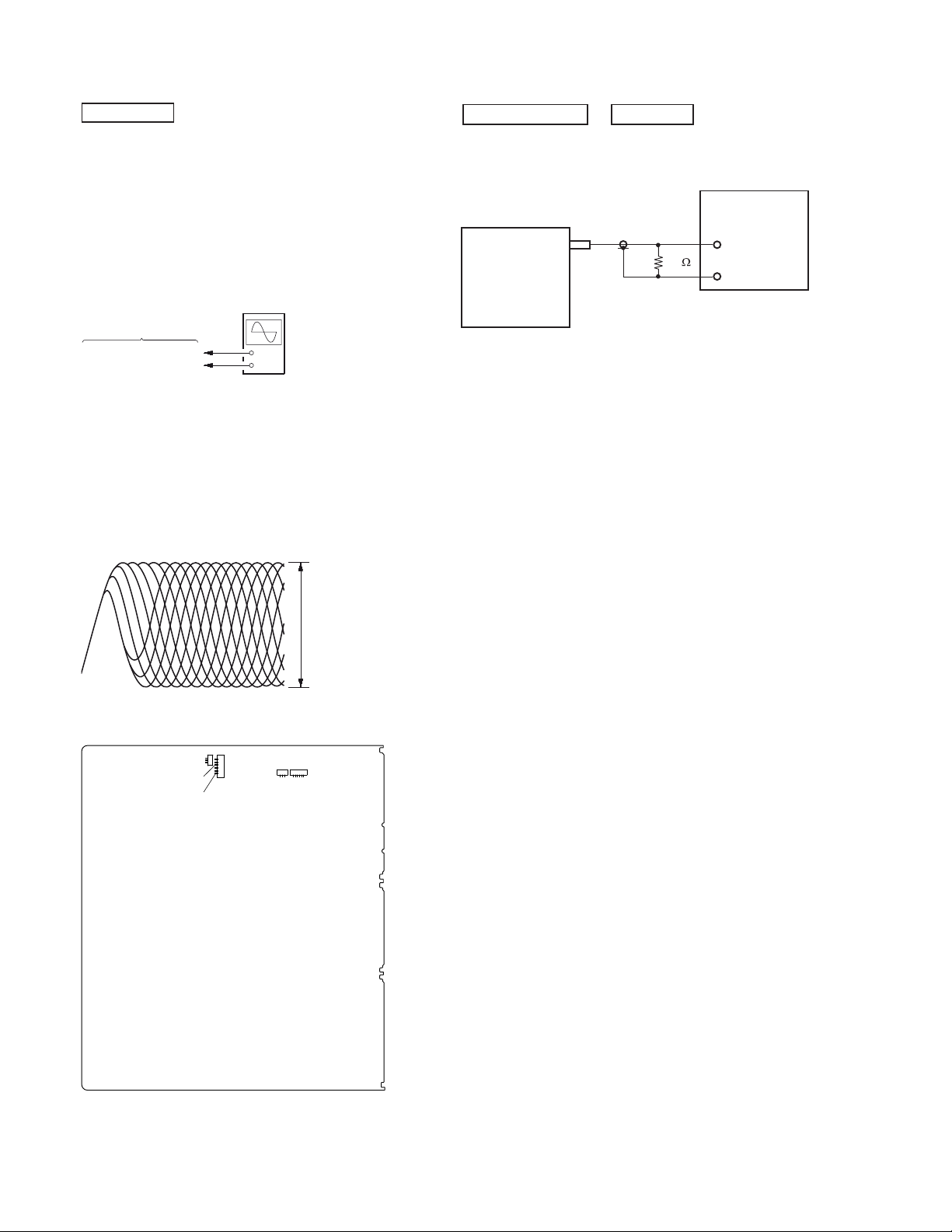
FOCUS BIAS CHECK
Procedure :
1. Connect the oscilloscope to CN507 pin 6 (RFMON) and
CN507 pin 3 (GND) on the MB board.
2. Press the [
?/1
STANDBY] button to turn the power on, and
press the [CD] button to select CD function.
3. Set disc (YEDS-18) and press the [
u
] button to playback.
4. Con
fi
rm that oscilloscope waveform is as shown in the fi gure
below (eye pattern).
A good eye pattern means that the diamond shape (
¡
) in the
center of the waveform can be clearly distinguished.
Checking Location:
-MB Board (Conductor Side)-
+
–
MB board
oscilloscope
(DC range)
CN507 pin 6 (RFMON)
CN507 pin 3 (GND)
VOLT/DIV: 200 mV
TIME/DIV: 500 ns
level:
1.0 ± 0.25 Vp-p (CD)
SECTION 4
ELECTRICAL CHECK
FM AUTO STOP CHECK
Procedure:
1. Turn the power on.
2. Input the following signal from Signal Generator to FM antenna input directly.
Carrier frequency : A = 87.5 MHz, B = 98 MHz, C = 108 MHz
Deviation : 75 kHz
Modulation : 1 kHz
ANT input : 35 dBu (EMF)
Note:
Please use 75 ohm “coaxial cable” to connect SG and the
set. You cannot use video cable for checking.
Please use SG whose output impedance is 75 ohm.
3. Set to FM tuner function and scan the input FM signal with
automatic scanning.
4. Con
fi
rm that input Frequency of A, B and C detected and
automatic scanning stops.
The stop of automatic scanning means “The station signal is
received in good condition”.
TUNER SECTION
0 dB = 1 V
signal
generator
set
+
–
75
CN891
CN590
CN507
CN509
pin 3 (GND)
pin 6 (RFMON)

HCD-GPX33/GPX55/GPX77/GPX88
17
SECTION 5
TROUBLESHOOTING
Switching Regulator Diagnosis Flow
The Output from Switching regulator is checked.
Is following power voltage up to standard?
Standby
Demo mode Power On
CN 201 pin1
CN 401 pin9
AC IN
Yes
No
Yes
END
No
Checks whether the state of a Cable and Outlet are normal.
If there are no problems, checks circumference circuit for
Main on/Sub on Output of Main mount side.
Replaces Switching regulator if it is not up to standard.
The Power Control signal to Switching regulator is checked.
Is following power voltage OK?
Main on/Sub on Standby Demo mode Power On
CN 201 :pin7 Low (0V) Hi (3.3V)
yy
Hi (3.3V)
13V±0.5V
13V±0.5V
0V 61V±2.5V
pin6 0V 23V±2.5V (HCD-GPX77/GPX88)
24V±2.5V (HCD-GPX33/GPX55)
pin4 0V -23V±2.5V (HCD-GPX77/GPX88)
-24V±2.5V (HCD-GPX33/GPX55)
pin1 0V -61V±2.5V
(1) AC input
(2) Fuse
(3) Sub Power transformer
(4) CN 201 Connector
pin1-2: 13V
pin3-4: GND
pin5: AC-DET
pin7: MAIN-ON
(5) MAIN Power transformer
(6) CN 401 Connector
pin1-3: V1- (DC-61V)
pin4: V2- (DC-24V)
pin5: GND
pin6: V2+ (DC+24V)
pin7-9: V1+ (DC+61V)
(2)
(1)
(4)
(6)
(3)
(5)
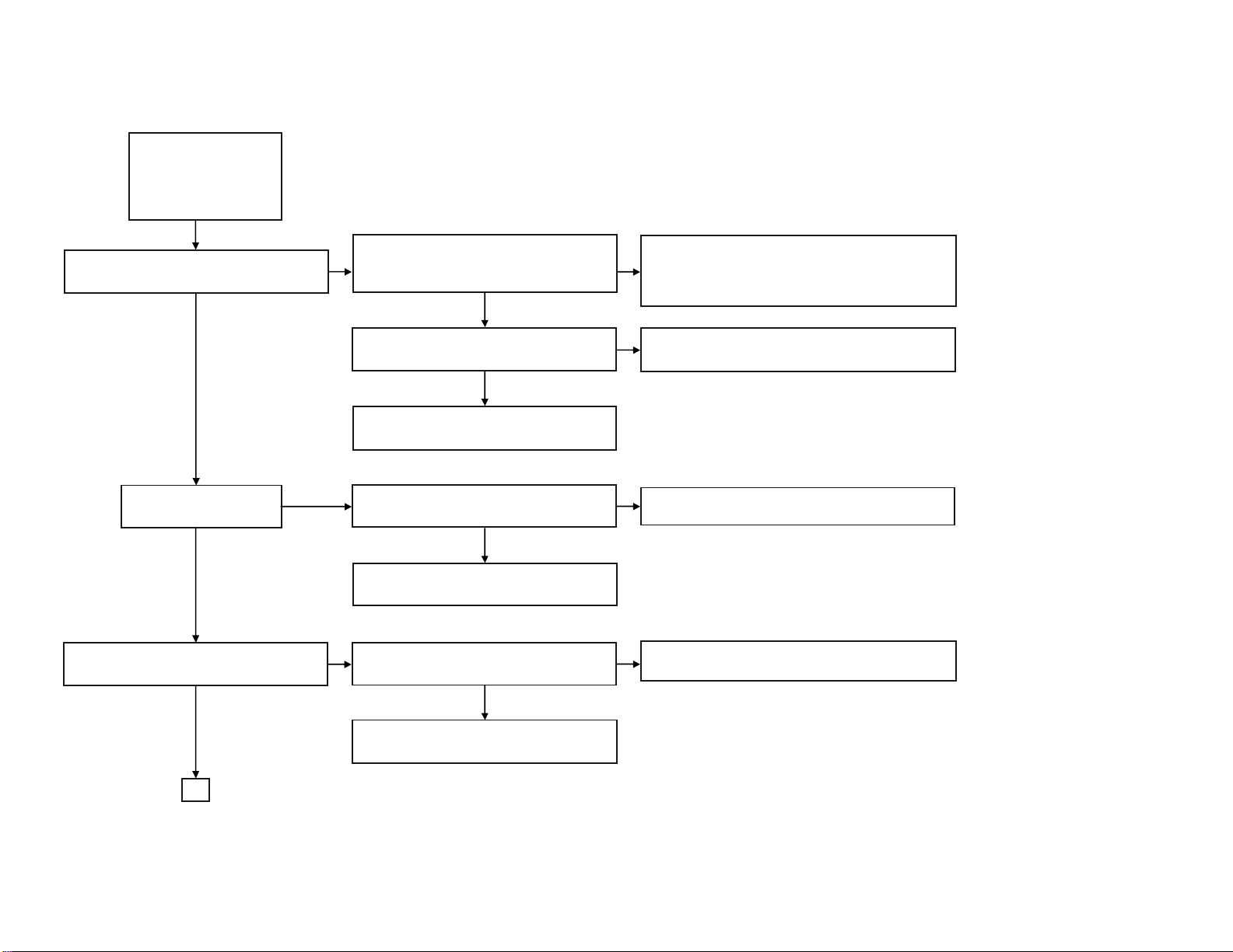
HCD-GPX33/GPX55/GPX77/GPX88
18
Optical Block Diagnosis Flow (1/2)
Does Optical pickup move to inner circumference?
(Visual check)
Yes
Yes
No
CL654: 1.2V
Check voltage supply to MTK IC501
CL577/CL656: 3.3V
Checks CN831 SL+/SL- signal.
Does it output the signal?
Does Spindle motor rotate?
(Visual check)
Yes
Does Optical pickup do focus search?
(Visual check)
No
Check condition of transistor Q354, V
E
§9C§9
If there is no problem, check circumference circuit of IC260
(switching regulator) for 3.3V.
Check IC651 (LDO IC) for 1.2V.
Yes
A
No
No
No
No
No
Checks circumference circuit for SL+/SL- of IC851.
Checks circumference circuit of IC501 FMO Signal.
Yes
Yes
Yes
REMOVE TOP PANEL
REMOVE SIDE PANEL
REMOVE CDM TOP PANEL
TURN ON
TRAY IN
The Sled motor has a problem.
Replaces BU.
Checks CN831 SP+/SP- signal.
Does it output the signal?
The Spindle motor has a problem.
Replaces BU.
Checks circumference circuit for SP+/SP of IC851.
Checks circumference circuit of IC501 DMO Signal.
Checks CN801 FCS+/FCS- signal.
Does it output the signal?
The Optical pickup has a problem.
Replaces BU.
Checks circumference circuit for FCS+/FCS- of IC851
Checks circumference circuit of IC501 FOO Signal.

HCD-GPX33/GPX55/GPX77/GPX88
19
Optical Block Diagnosis Flow (2/2)
Does laser diode become luminous ?
(Visual check)
Is output level of RF signal (CN507 6pin) up to standard?
RF Level = 1.0 ±0.25 Vpp
Test CD:YEDS-18
Is there no problem with Long term Aging Test (60min)?
Confirms that there is no sound skip.
END
No
No
Check JL802 (LD650) signal
Does it output 2.2V when laser become luminous?
Check JL806 (LD780) signal
Does it output 1.8V when laser become luminous?
Checks circumference circuit of Q881 or Q891.
Checks circumference circuit of IC501 LDO1 and LDO2.
The Optical pickup has a problems.
Replaces BU.
DISC IN
No
A
Is output level of RF signal(CN507 6pin) up to standard?
RF Level = 1.0 ±0.25 Vpp
Test CD:YEDS-18
Replaces BU if it is not up to standard.
No
No
If it is not up to standard,
Lens cleaning is performed.
The Optical pickup has a problems.
Replaces BU.
Yes
Yes
Yes
Yes
Yes
Yes
Yes

HCD-GPX33/GPX55/GPX77/GPX88
20
D-AMP Mount Diagnosis Flow (1/2)
PLAY MUSIC
Is there audio output from D-AMP Board?
Checks 13.5V output of CN200 1pin.
Is the power voltage OK?
Checks 3V output of CN200 6pin(Main on)
Is the power voltage OK?
Checks 61V output of CN1001 1pin(PVDD).
Is the power voltage OK?
Checks OUT terminal-49V output of REG IC1000
Or, Checks GND and OUT Terminal with Tester.
Is it shorted out?
Reinserts the cable or Exchanges.
If there are no problems, Checks output of
Switching regulator Board.
Reinserts the cable or Exchanges.
If there are no problems, Checks Output of
Main on Output of Main Board side.
Reinserts the cable or Exchanges.
If there are no problems, Checks output of
Switching regulator Board.
Checks circumference circuit of REG IC1000.
If there are no problems, exchanges IC1000.
A
B
Yes
No
Yes
Yes
Yes
Yes
Yes
No
No
No
No
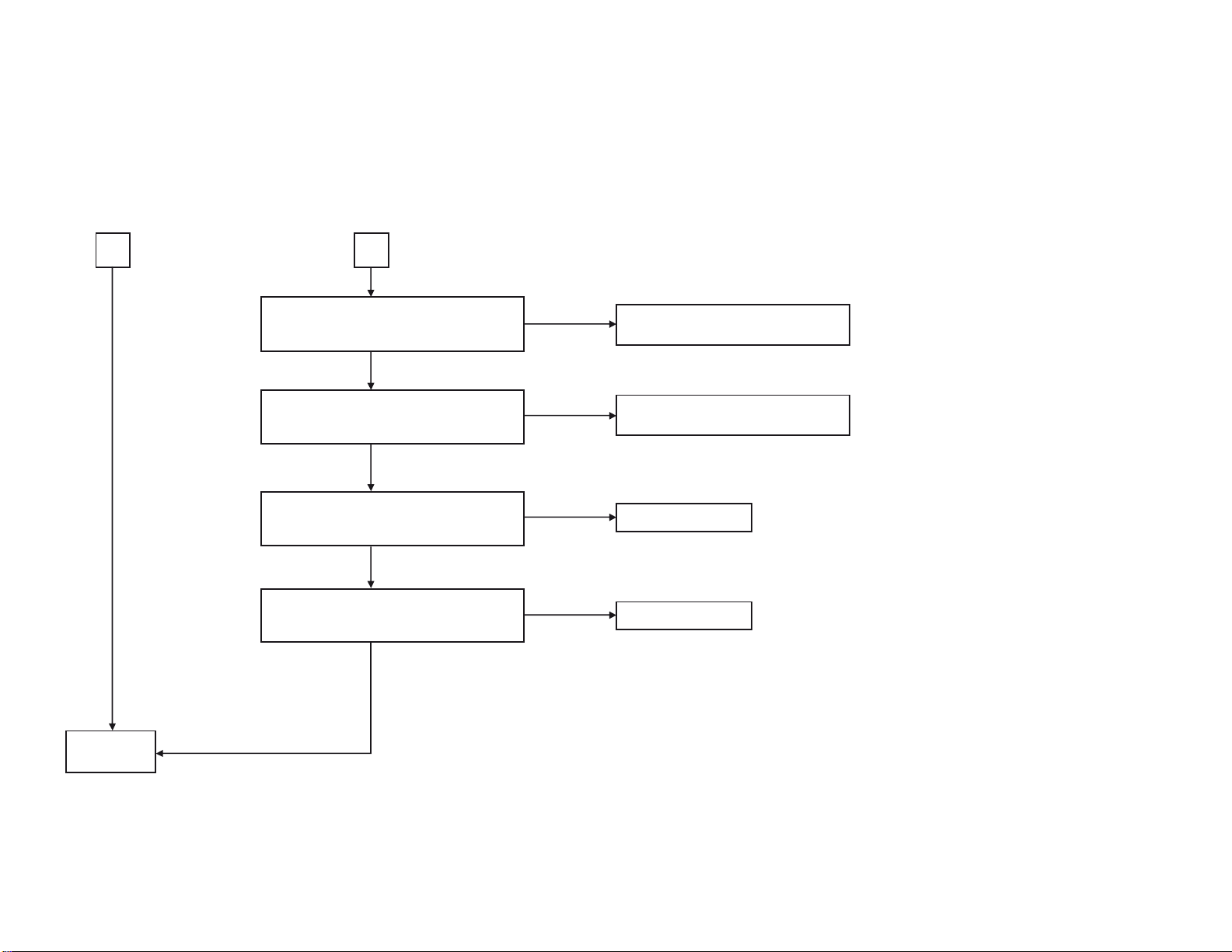
HCD-GPX33/GPX55/GPX77/GPX88
21
D-AMP Mount Diagnosis Flow (2/2)
END
Checks OUT Terminal 5V output of REG IC1009 or,
Checks GND and OUT Terminal with Tester.
Is it shorted out?
Assembles into the unit again then ,checks
whether there is the audio output from
D-AMP Board.
Checks circumference circuit of REG IC1009.
If there are no problems, exchanges IC1009.
Checks circumference circuit of REG IC1010.
If there are no problems, exchanges IC1010.
Replaces D-AMP Board
Replaces D-AMP Board
A
B
Yes
Yes
Yes
Yes
No
No
No
No
Checks OUT Terminal -5V output of REG IC1010 or,
Checks GND and OUT Terminal with Tester.
Is it shorted out?
Leave D-AMP Mount to a state of it only and,
checks Power Audio Driver (MOS FET) with Tester.
Is it shorted out?
¢
Refer to Page 22).

HCD-GPX33/GPX55/GPX77/GPX88
22
MOSFET Confi rmation for D-AMP Mount
IC851
IC1002
IC1001
IC1008
1
12
1324
IC1502
114
78
22 21
29
28 1530
JRJRJRJRJRJRJR
C20
C1118
C1502
C1504
CL891
CL892
C1121
C1122
C1123
C1318
C1319
C1514
C1516
C1136
C45
C46
C1526
C48
C1528
C1145
R622
C1147
L1004
R624
R1508
C1149
R1509
C1534
C1537
C1150
C1538
C1151
C1152
JL1570
C400
C1542
JL1576
R1137
C1161
C601
C1162
C1163
R1523
C1164
C604
R1524
JL201
R1525
R1332
JL203
R1333
R1334
R838
R1335
R1336
JL206
R1337
JL5022
R1147
C1558
R1530
R840
R1148
R1531
R1532
R1533
R1534
C1174
R1535
R1342
R1344
JL214
R1151
R1346
R1153
R1154
R1349
R1155
R1156
R1157
R850
R851
C1184
R854
R1351
R1354
JL801
JL802
JL803
R1164
R474
JL804
JL805
JL806
JL807
JL808
JL809
JL422
JL231
JL233
JL234
JL810
R1170
R1364
JL811
JL812
R1172
JL813
JL814
JL815
JL816
JL817
JL818
R1178
JL819
R1179
C837
R1370
C839
R1372
R1374
JL244
JL820
R878
R1180
JL821
R1569
JL822
R1182
R1377
JL823
R1183
JL824
R1379
R1570
R1573
R1574
JL831
R1579
R1386
JL832
R1193
CL547
JL833
R1388
JL834
R1195
C851
JL835
JL836
C854
R1581
JL1002
C858
R1585
JL1006
R1587
JL264
JL1009
R1397
R1399
JL460
JL1010
JL461
JL1011
JL462
JL1012
JL463
JL1013
C480
C481
C869
JL273
1
3
CN891
C873
C876
C877
JL1600
JL1601
CL571
JL1025
JL1602
CL572
JL1603
CL573
CL574
CL576
CL577
CL578
CL579
JL1039
C1005
C1007
C1009
JL681
JL682
JL683
JL1040
JL684
JL685
D837
JL1044
C1011
CL591
D839
JL1045
CL592
JL1046
JL1047
CL593
JL1048
CL594
R109
JL1049
CL595
CL596
R301
R303
R110
JL1050
R111
JL1051
R112
JL1052
R113
R114
R115
JL1055
R116
JL1056
R501
R1000
R1001
R505
R311
R1002
R312
R1003
R313
JL1060
D1008
D1009
R1005
JL1061
JL1062
R1008
C1030
JL1067
JL1068
C1034
R510
Q1031
E
C1229
C1035
R705
C1036
2
91
8
CN110
R320
Q1034
C1615
E
E
Q1035
C1617
Q1037
E
R1013
C1230
JL1070
D1019
R1015
R325
JL1071
JL1072
R132
R1018
JL1074
R1401
JL1651
JL1652
JL1653
C1237
JL1077
C1620
JL1654
C1238
JL1078
R1405
JL1655
C1239
R1406
JL1656
R1212
CN507
R1214
R1020
Q1045
CN509
D1025
R1022
D1026
D1027
R1024
D1028
C1240
JL1080
R1025
JL1081
JL1082
R1026
R1027
JL1083
R1028
C1050
JL1084
C1051
R1029
JL1085
C1052
R722
JL1086
JL1087
C1053
JL1088
C1054
C300
C1055
C301
JL1089
Q1051
E
C1056
R1030
R534
R1031
R1032
R1034
C114
JL1090
JL1091
R1612
R1036
R1613
R1037
R1614
R1038
R1615
C1061
C501
C1062
C1063
JL1097
C503
R157
C1064
C311
R1232
C1066
C506
R542
C1067
R1428
R1234
C1068
C508
R1429
D1047
R1620
R1621
R1239
R1622
C702
R1623
R1047
R1430
C510
R164
R1431
R1049
R165
R741
R1432
C1266
C1268
R1628
JL110
R1240
C320
C1269
JL111
R1629
C515
JL112
C516
JL113
C517
R1050
C518
JL114
JL115
C325
C519
R749
JL116
JL117
R1053
C1270
R1630
JL118
R1054
R1631
R1055
C711
R27
C1274
R1058
JL504
R28
C1275
R1059
C521
C715
C1278
C1084
C524
JL121
C1085
C525
JL122
C1086
R1252
C526
JL123
C1087
R1253
C527
JL124
R1254
C1088
C528
JL125
C1089
C529
JL126
JL127
C1280
JL128
R950
C1281
C1282
C916
C1283
R1643
C1284
R1644
C1090
C1285
R1645
C1091
R39
C1286
R1646
C1092
C1287
C1093
C1288
C1289
JL131
JL132
JL133
JL134
JL135
JL136
JL137
C1290
JL138
C731
JL139
C733
C736
JL140
C739
R390
R971
C741
R395
R1086
R972
C742
C743
R1087
R973
R1088
R974
R1089
JL151
JL152
JL154
R594
R1094
R1288
R1095
R1289
R1099
R69
JL353
JL160
R1290
R1291
JL161
JL162
R1292
JL163
JL164
JL165
JL167
JL1100
JL168
JL1101
JL169
JL1103
16
CN590
JL1105
CL845
JL940
JL170
CL654
JL941
JL171
CL462
JL942
JL172
CL656
JL943
JL173
JL944
JL174
JL175
JL176
Q422
JL177
JL178
JL179
C390
JL181
JL182
JL183
JL184
C395
JL185
JL186
JL1506
JL187
C973
JL1507
JL188
C974
JL1508
JL189
C975
R95
JL1509
C976
JL57
JL190
JL1510
JL191
JL1511
JL192
JL1512
JL1513
C598
JL1514
C599
JL1515
JL1516
JL1517
JL1518
JL1519
JL390
JL391
C1102
JL1520
JL395
JL1521
JL396
JL1522
C1107
JL1523
C1108
JL1524
C1109
18
CN1502
C1111
14
CN1505
C1112
C1307
C1308
JL1530
JL1531
R1435
D1050
D1052
F001
F002
FB701
FB211
FB213
FB210
FB265
D460 D461 D462
C1510
C1522
C288
R1365
R1437
C750
GPX88
GPX77
GPX77/GPX88GPX88
GPX77/
GPX88
SUBWOOFERS
LED SPEAKERS
R
FRONT
SPEAKERS
R
GPX88
GPX88
GPX88
GPX88
GPX88
GPX88
GPX77
GPX55/GPX77/
GPX88
FLASH
PROGRAMMING
FLASH
PROGRAMMING
FLASH
PROGRAMMING
FLASH
PROGRAMMING
FLASH
PROGRAMMING
B2
E2
C1
B1
C2
E1
Test er
Tester
Test er
Tester
Test er
Tester
<Note>
Please check each channel’s resistance value for the Coil’s terminal and Capacitor’s + and – terminal.
These terminal is equal to resistance value for POWER AUDIO DRIVER terminal.
Short = NG
Tester
Tester
HCD-GPX33/GPX55/GPX77/GPX88
HCD-GPX33/GPX55/GPX77/GPX88
2323
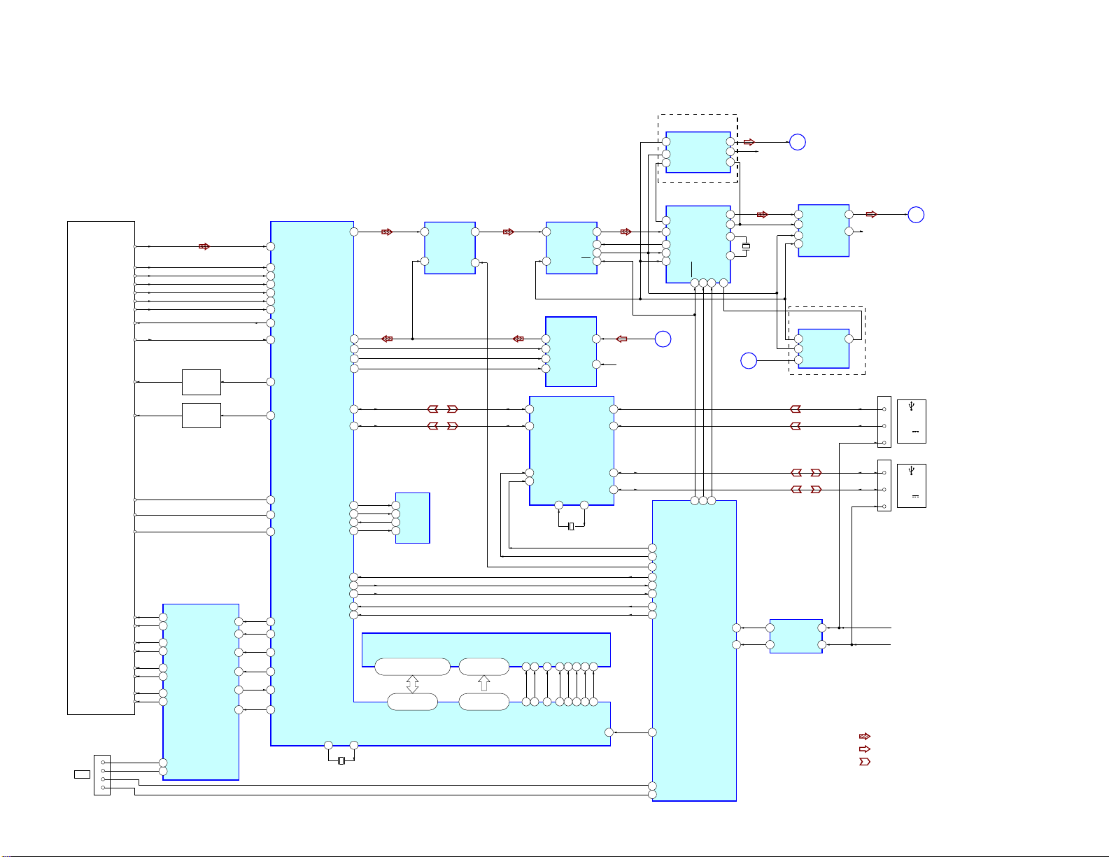
6-1. BLOCK DIAGRAM - CD/USB Section -
SECTION 6
DIAGRAMS
SERVICE,
OPTICAL DEVICE
CD RF AMP
FOCUS/TRACKING ERROR AMP
CD SYSTEM PROCESSOR
DIGITAL SERVO PROCESSOR
IC501
SYSTEM
CONTROLLER
IC100 (1/4)
5CH SYSTEM
MOTOR DRIVER
IC851
AUTO
POWER CTRL
Q891
RFIP
RF_C1
128
127
RF_B
RF_A
RF_D2
RF
VOA/A
VOB/B
VOC/C
VOD/D
RF_F4VOE/E+G
RF_E3VOF/F+H
V2O
10
VC
LDO114LD(780)
AUTO
POWER CTRL
Q881
LDO215LD(650)
FOO22
VR(780)
DVD_VR20
CD_VR19
MSW23
VR(650)
FCS+
(LO:DVD,HI:CD)MSW
MDI1
13
PD
64M SDRAM
IC504
X501
27MHz
14
FCS–
13
1
TRO21
TRK+
16
TRK–
15
26
FMO18
SL+ 17
SL– 18
23
DMO17
SP+ 11
SP– 12
9
10
4
V14/VREF01127
DG0, DQ1 – DQ15
RD0 – RD15
PRST#
A0 – A11
RA0 – RA11
2, 4, 5, 7, 8, 10, 11, 13, 42,
44, 45, 47, 48, 50, 51, 53
52 – 55, 57 – 60,
69 - 62
89 - 92, 79 - 74,
88, 73
23 – 26,
29 – 34, 22, 35
XTALI
7
BA0 BA0
85
20
BA1 BA1
86
21
RCLK CLK
72
38
DQM0 LDQM
61
15
DQM1 UDQM
70
39
RAS# RAS
83
18
CAS# CAS
82
17
RWE# WE
80
16
MUTE4528
38
XTALO
8
USB CONTROLLER
IC300
31
USBDP_UP
30
USBDM_UP
USB_DP 25
USB_DM 24
2USBDP_DN1
1USBDM_DN1
84/I-HUB-OC-USB B
CN2102
3
2
1
86
/I-HUB-OC-USB A
USB
COMPARATOR
IC280
USBA+5V
USBB+5V
4USBDP_DN2
3USBDM_DN2
3
2
1
O-MTK-RESET57
I-CDM-LOAD-SW63
I-CDM-UNLOAD-SW64
O-MTK-SDO
45
I-MTK-SDI
46
I-MTK-CLK
47
I-MTK-XIFCS
56
O-MTK-BUSY
55
IFSDI 40
IFSDO 35
IFSCK 34
IFCS# 42
IFBSY 41
O-HUB-RESET
88
O-HUB-VBUS-DETECT
87
VBUS_DET27
RESET_N26
X300
24MHz
XTALIN
33
XTALOUT
32
CN2103
1
7
3
5
SF_CS#
_CS
30
1
SF_CK
SCK
33
6
EEPROM
IC502
SO
2
SI
5
SF_DO
31
SF_DI
32
ACLK
ALRCK
ABCK
ADIN
118
L-OUT
ASDATA0
113
14
13
STEREO A/D CONVERTER
IC920
8
L-IN
D+
D-
VBUS
D+
D-
VBUS
R-CH
117
7
112
6
106
9
VOUTL
8
7
VOUTR
STEREO A/D CONVERTER
IC750
2
DATA
1
BCK
3
LRCK
16
SCK
DOUT
9
STEREO A/D CONVERTER
IC900
6
SCKI
7
LRCK
13
VINL
23
27
AUDIO DSP
IC701
11
22
19
21
25
23
24
13
ASYNCHRONOUS SAMPLE
RATE CONVERTER
IC740
4
6
5
SIGNAL SELECTOR
IC780
2
1
R-CH
61
48 75 76
32 15 16 12
SDIN1
26
SDOUT2
SDA1
SCL1
SDIN2
LRCK
MCLKO
SCLKOUT1
SCLKOUT2
SDOUT1
4
3
XTALO
XTALI
RESET
8
7
STEREO A/D CONVERTER
IC765
16
3
2
SCK
DATA
LRCK
VOUTR
1
BCK
VOUTL
2
RCKI
SDIN
RST
SDOUT
LRCKO
BCKO
B
A
Y
SEL
SCKI
LRCK
BCK
DOUT
VINL
VINR
O-DIGITAL-SEL
I-DSP SDA
I-DSP SCL
O-DSP-RESET
VOFC+
VOFC-
VOTKVOTK+
VOLD+
VOLD-
VOSL+
VOSL-
VINFC
VINTK
VINLD
VINSL+
BIAS
MUTE
VOTR-
VOTR+
L-OUT
R-CH
123
CN681
5
1
2
3
CDM
X762
12.288MHz
LOADLOAD+
TRAY-IN
TRAY-OUT
500mA
5V
B
REC/PLAY
500mA
5V
A
PLAY
GPX55/GPX77/GPX88
GPX88
‡6LJQDOSDWK
: CD PLAY
: AUDIO
: USB
‡5FKLVRPLWWHGGXHWR
VDPHDV/FK
MAIN
SECTION
(Page 24)
A
MAIN
SECTION
(Page 24)
B
MAIN
SECTION
(Page 24)
C
MAIN
SECTION
(Page 24)
D
HCD-GPX33/GPX55/GPX77/GPX88
HCD-GPX33/GPX55/GPX77/GPX88
2424
6-2. BLOCK DIAGRAM - MAIN Section -
FM DRIVER
(FM RECEIVER)
IC460
FRF1
ARF2
L OUT
R OUTDAR-CH
CK
ANTENNA
FM/AM
IIC/RDSI
43
I-ST-RDS
13
12
28
I-ST-DATA
27
I-ST-CLK
O-ANALOG-BSEL
52
O-ANAL0G-ASEL
51
I-MIC-DETECT
91
SYSTEM CONTROLLER
IC100 (2/4)
J2050
MIC
RV2050
MIC AMP
IC2050
L-OUT
L-OUT
SW OUT L
FRONT-L
7513
13
I-XIN
11O-XOUT
X11
8MHz
8
I-X-CIN
9
O-XC-OUT
1
O-RGB-GREEN
24
O-RGB-BLUE
5
O-RGB-SCLK
80O-RGB-TRANS-LED-SPK
3
O-RGB-SOUT
X9
32.768kHz
13
OP AMP
IC950
2
5
11
8
6
13
OP AMP
IC951
MIC DRIVER
Q2050,Q2051
MIC LEVEL
MIN MAX
SWITCH SIGNAL
SELECTOR
Q1600
AUDIO IN
R-CH
R
L
J1600
PC/
GAME
R-CH
TV/DVD/
SAT
ARF1
4
CN460
17
X2
16
X1
X460
12MHz
CD/USB
SECTION
(Page 23)
A
MAIN
SECTION
(Page 24)
G
CD/USB
SECTION
(Page 23)
B
AMP
SECTION
(Page 25)
E
AMP
SECTION
(Page 25)
F
L-IN
CD/USB
SECTION
(Page 23)
C
‡6LJQDOSDWK
: AUDIO
: TUNER (FM/AM)
: MIC
‡5FKLVRPLWWHGGXHWR
VDPHDV/FK
SIGNAL SELECTOR
IC1600
X0 B
X1
X3
X2
12
9
X
13
A
10
15
14
11
BLUETOOTH AMP.
IC320
-OUT
RCH_N
RCH_P
LCH_P
LCH_N
BT-RDX
BT-TDX
3.3V
+
-
67
OUT
1
5
+
3
2
L-CH
R-CH
CD/USB
SECTION
(Page 23)
D
CN180
4
5
2
3
8
9
12
BLUETOOTH
MAIN
SECTION
(Page 24)
G
L-CH
R-CH
I-BT-RXD
O-BT-ON
34
21
O-BT-TXD
33
BLUETOOTH
POWER CONTROL
Q355, Q356
LED SELECTOR
IC1502
TRANS
SCK
SIN
4
3
2
LED SELECTOR
IC1501
TRANS
SCK
SIN
4
3
2
/OUT2
GREEN_LED
GREEN_LED
BLUE_LED
RED_LED
GREEN_LED
BLUE_LED
RED_LED
R-CH
BLUE_LED
RED_LED
/OUT1
/OUT0
7
6
5
/OUT12
/OUT11
/OUT10
17
16
15
/OUT15
/OUT14
/OUT13
20
19
18
L
CN1506
2
4
3
R
SUBWOOFERS
CN1505
2
4
3
R-CH
L
R
FRONT
SPEAKERS
LED
SPEAKERS
GPX77/GPX88
GPX77
GPX88
LED DRIVER
Q422, Q423
CN1504
6
4
8
7
3
2
CN1502
6
4
8
7
3
2
GPX55/GPX77/GPX88

HCD-GPX33/GPX55/GPX77/GPX88
HCD-GPX33/GPX55/GPX77/GPX88
2525
6-3. BLOCK DIAGRAM - AMP Section -
TB1000
/I-FAN BLOCK
+
-
14
11
POWER AMP
IC1004
3
5
IN
HO
CSD
LO
POWER AUDIO
DRIVER
Q1015
TH1000
RESET
SWITCH
Q1008
MUTE
DRIVER
Q1048
MUTE
DRIVER
Q902
MUTE
SWITCH
Q330
PROTECTION
SWITCH
Q1000, Q1001,
Q1050, Q1051
Q1035
PROTECTION
SWITCH
D1026, D1028, D1047
SD SWITCH
Q1005
14
11
POWER AMP
IC1006
3
5
IN
HO
CSD
LO
PROTECTION
SWITCH
Q1020, Q1027,
Q1056, Q1057
TH1003
SUBWOOFERS
,03('$1&(86(
SUBWOOFERS
,03('$1&(86(
FRONT SPEAKERS
,03('$1&(86(
R
L
RESET
SWITCH
Q1009
SD SWITCH
Q1006
OR AMP
IC1001
OR AMP
IC1002
OR AMP
IC1008
TB1001
+
-
14
11
POWER AMP
IC1003
3
5
IN
HO
CSD
LO
TH1001
RESET
SWITCH
Q1007
SD SWITCH
Q1036
SD SWITCH
Q1038
14
11
POWER AMP
IC1005
3
5
IN
HO
CSD
LO
TH1002
R
L
RESET
SWITCH
Q1010
DC FAN
FAN DRIVER
Q1037, Q1045
SYSTEM CONTROLLER
IC100 (3/4)
D1018
69
68
PROTECTION
SWITCH
Q1055
THERMISTER
SWITCH
Q1030, Q1031
RESET SWITCH
Q1004, Q1033,
Q1029
7073
50
7
4
5
3
18
74
18
AOUT
V+ V-
INB+
INA+
BOUT
AOUT
V+ V-
BOUT
SW OUT L
R-CH
R-CH
FRONT-L
O-SW MUTE
20
O-DAMP-CLK
O-DAMP-RESET
/I-THERMISTOR-DET
71
/I-DC-DET
I-FAN-DRIVE
49
O-FRONT-MUTE
74
/I-SD-FAST
72
I-DAMP-OCP
PROTECTION
SWITCH
Q1032
POWER AUDIO
DRIVER
Q1018
POWER AUDIO
DRIVER
Q1011
POWER AUDIO
DRIVER
Q1014
D1008 D1009
TB1002
-
MAIN
SECTION
(Page 24)
E
MAIN
SECTION
(Page 24)
F
5
3
INB+
INA+
1
AOUT
2
INA-
3
INA+
GPX55/
GPX77/GPX88
GPX88
GPX55/GPX77/GPX88
GPX77/GPX88 GPX55
‡6LJQDOSDWK
: AUDIO
‡5FKLVRPLWWHGGXHWR
VDPHDV/FK
Q1034
PROTECTION
SWITCH
D1025, D1027, D1046
POWER AUDIO
DRIVER
Q1016
POWER AUDIO
DRIVER
Q1017
POWER AUDIO
DRIVER
Q1012
POWER AUDIO
DRIVER
Q1013
 Loading...