

Sony DNE-1 Service manual
D-NE1/NE9
SERVICE MANUAL
Ver 1.5 2004.08
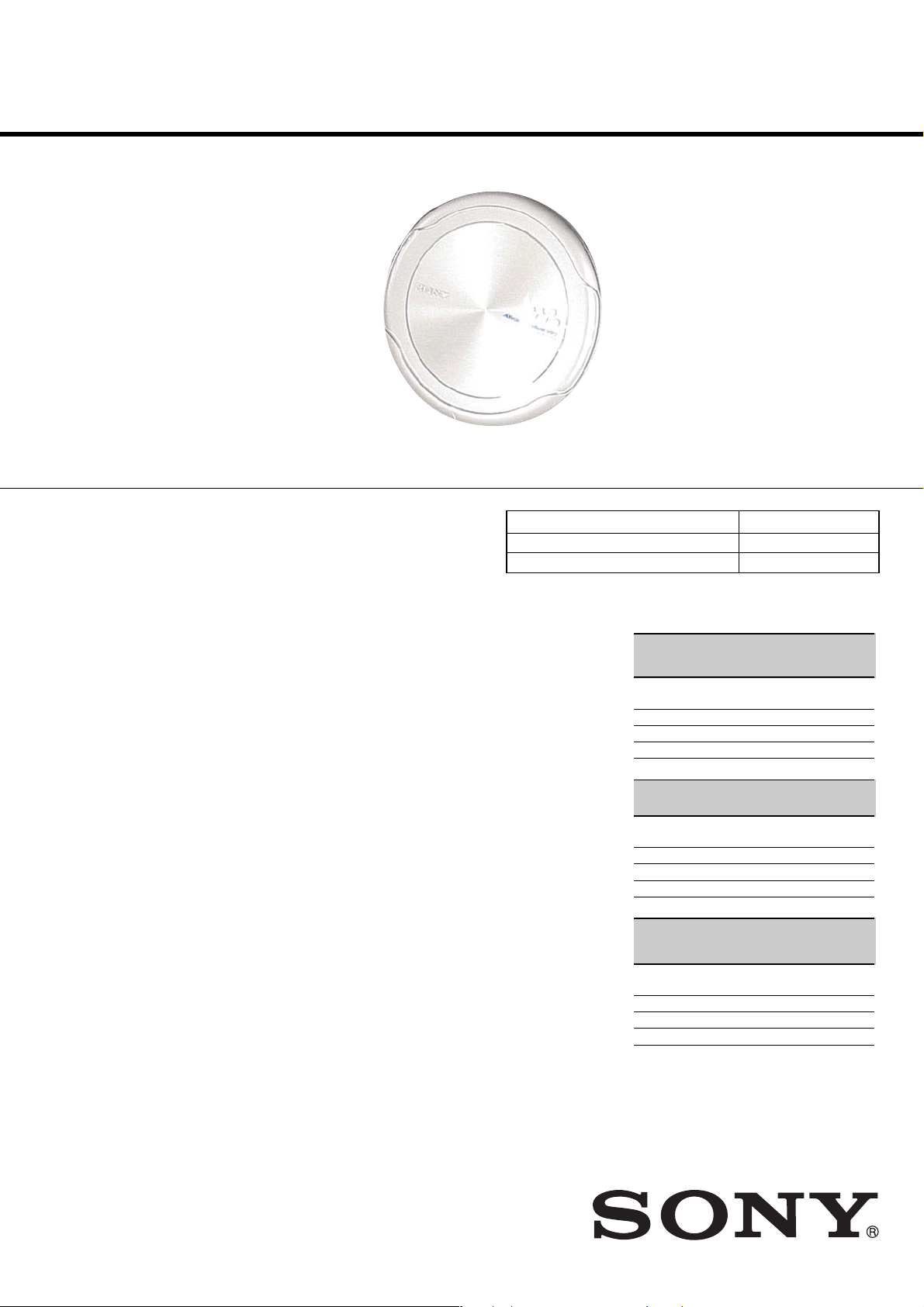
Photo : D-NE9
US and foreign patents licensed from
Dolby Laboratories.
SPECIFICATIONS
US Model
D-NE1
Canadian Model
AEP Model
D-NE1/NE9
UK Model
D-NE1
E Model
Australian Model
Chinese Model
Tourist Model
D-NE1/NE9
Model Name Using Similar Mechanism NEW
CD Mechanism Type CDM-3325ER2
Optical Pick-up Name DAX-25E
System
Compact disc digital audio system
Laser diode properties
Material: GaAlAs
Wavelength: λ = 780 nm
Emission duration: Continuous
Laser output: Less than 44.6 µW
(This output is the value measured at a distance
of 200 mm from the objective lens surface on
the optical pick-up block with 7 mm aperture.)
D-A conversion
1-bit quartz time-axis control
Frequency response
20 - 20 000 Hz
307)
Output (at 4.5 V input level)
Line output (stereo minijack)
Output level 0.7 V rms at 47 kΩ
Recommended load impedance
Headphones (stereo minijack)
Approx. 5 mW +
(Approx. 1.5 mW +
*For the customers in Europe
Optical digital output (optical output connector)
Output level: –21 - –15 dBm
Wavelength: 630 - 690 nm at peak level
+1–2
dB (measured by JEITA CP-
over 10 kΩ
Approx. 5 mW at 16 Ω
Approx. 1.5 mW at 16 Ω)*
Power requirements
For the area code of the model you
purchased, check the upper left side of the
bar code on the package.
•Two Sony NH-14WM (A) rechargeable
batteries: 1.2 V DC × 2
•Two LR6 (size AA) batteries: 1.5 V DC × 2
•AC power adaptor (DC IN 4.5 V jack):
Canadian and Taiwan models:
US,
120 V, 60 Hz
UK model: 230 V, 50 Hz
Australian model: 240V , 50 Hz
AEP, Tourist, E18, Korean and East Europe models:
100 - 240 V, 50/60 Hz
Hong Kong model: 230 V, 50 Hz
Chinese model: 220 V, 50 Hz
Battery life*1 (approx. hours)
(When you use the CD player on a flat and stable
surface)
Playing time varies depending on how the CD
player is used.
When using two NH-14WM (A) (charged for
about 5 hours*
< > : NH-10WM
Audio CD 35 < 25 >32 < 23
ATRAC3plus file*
MP3 file*
When using external battery case (two alkaline
batteries*
Audio CD 55 50
ATRAC3plus file*
MP3 file*
When using two NH-14WM (A) and external
battery case (two alkaline batteries*
< > : NH-10WM
Audio CD 90 < 80
ATRAC3plus file*
MP3 file*
•Abbreviation
E18: 100-230V AC area in E model
2
)
G-PROTECTION
“1” “2”
3
3
3
55 < 40 >55 < 40
50 < 35 >50 < 35
G-PROTECTION
“1” “2”
95 95
85 85
G-PROTECTION
“1” “2”
150 <
135 >
135 <
120 >
4
5
)
4
4
— Continued on next page —
5
)
> 82 < 73
150 <
135 <
>
>
>
>
135 >
120 >
9-877-308-06
2004H16-1
© 2004.08
PORTABLE CD PLAYER
Sony Corporation
Personal Audio Company
Published by Sony Engineering Corporation
D-NE1/NE9
*1 Measured value by the standard of JEITA (Japan
Electronics and Information Technology
Industries Association)
*2 Charging time varies depending on how the
rechargeable battery is used.
*3 Recorded at 48 kbps or 64 kbps
*4 Recorded at 128 kbps
*5 When using Sony alkaline batteries LR6 (SG)
(produced in Japan)
Operating temperature
5°C - 35°C (41°F - 95°F)
Dimensions (w/h/d) (excluding
projecting parts and controls)
Approx. 135.4 × 135.4 × 15.8 mm
(5 3⁄8 × 5 3⁄8 × 5⁄8 in.)
Mass (excluding accessories)
Approx. 179 g (6.4 oz.)
Supplied accessories
AC power adaptor (1)
Rechargeable batteries (2)
Battery carrying case (1)
Headphones / earphones (1)
Remote control (1)
Charging stand (1)
Carrying pouch (1)
External battery case (1)
CD-ROM (Sonic Stage Simple Burner) (1)
User’s guide for Sonic Stage Simple Burner (1)
Design and specifications are subject to change
without notice.
This appliance is classified as a CLASS 1 LASER product.
The CLASS 1 LASER PRODUCT MARKING is located on
the rear exterior.
TABLE OF CONTENTS
1. SERVICING NOTE ·························································· 3
2. GENERAL ·········································································· 5
3. DISASSEMBLY ································································7
3-1. Upper Lid Section ·························································7
3-2. Cabinet (upper) Section················································· 8
3-3. MAIN Board,
CD Mechanism Section (CDM-3325ER2)···················· 9
3-4. Motor Assy (Spindle) (M901), Motor Assy (Sled)
(M902) Optical Pick-Up Assy (DAX-25E) ·················10
4. ELECTRICAL CHECKING········································· 11
5. DIAGRAMS······································································ 12
5-1. Block Diagram ···························································· 13
5-2. Printed Wiring Boards – MAIN Board (Side A) – ······14
5-3. Printed Wiring Boards – MAIN Board (Side B) – ······ 15
5-4. Schematic Diagrams – MAIN Board (1/4) –··············· 16
5-5. Schematic Diagrams – MAIN Board (2/4) –··············· 17
5-6. Schematic Diagrams – MAIN Board (3/4) –··············· 18
5-7. Schematic Diagrams – MAIN Board (4/4) –··············· 19
5-8. IC Block Diagram ······················································· 20
5-9. IC Pin Function Descriptions ······································ 21
6. EXPLODED VIEWS ······················································26
7. ELECTRICAL PARTS LIST ······································· 29
CAUTION
Use of controls or adjustments or performance of procedures
other than those specified herein may result in hazardous
radiation exposure.
Flexible Circuit Board Repairing
•Keep the temperature of the soldering iron around 270 ˚C dur-
ing repairing.
• Do not touch the soldering iron on the same conductor of the
circuit board (within 3 times).
• Be careful not to apply force on the conductor when soldering
or unsoldering.
Notes on chip component replacement
•Never reuse a disconnected c hip component.
• Notice that the minus side of a tantalum capacitor may be dam-
aged by heat.
On AC power adaptor
•Use only the AC power adaptor supplied or
recommeded in “Accessories (supplied/
optional).” Do not use any other AC power
adaptor. It may cause a malfunction.
Polarity of the plug
Unleaded solder
Boards requiring use of unleaded solder are printed with the leadfree mark (LF) indicating the solder contains no lead.
(Caution: Some printed circuit boards may not come printed with
the lead free mark due to their particular size.)
: LEAD FREE MARK
Unleaded solder has the following characteristics.
• Unleaded solder melts at a temperature about 40°C higher than
ordinary solder.
Ordinary soldering irons can be used but the iron tip has to be
applied to the solder joint for a slightly longer time.
Soldering irons using a temperature regulator should be set to
about 350°C.
Caution: The printed pattern (copper foil) may peel away if the
heated tip is applied for too long, so be careful!
• Strong viscosity
Unleaded solder is more viscous (sticky, less prone to flow) than
ordinary solder so use caution not to let solder bridges occur such
as on IC pins, etc.
• Usable with ordinary solder
It is best to use only unleaded solder but unleaded solder may
also be added to ordinary solder.
2
SECTION 1
SERVICING NOTE
D-NE1/NE9
NOTES ON HANDLING THE OPTICAL PICK-UP
BLOCK OR BASE UNIT
The laser diode in the optical pick-up block may suffer electrostatic
breakdown because of the potential difference generated by the
charged electrostatic load, etc. on clothing and the human body.
During repair, pay attention to electrostatic breakdown and also use
the procedure in the printed matter which is included in the repair
parts.
The flexible board is easily damaged and should be handled with
care.
NOTES ON LASER DIODE EMISSION CHECK
The laser beam on this model is concentrated so as to be focused on
the disc reflective surface by the objective lens in the optical pickup block. Therefore, when checking the laser diode emission,
observe from more than 30 cm away from the objective lens.
SAFETY-RELATED COMPONENT WARNING!!
COMPONENTS IDENTIFIED BY MARK 0 OR DOTTED LINE WITH
MARK 0 ON THE SCHEMATIC DIAGRAMS AND IN THE PARTS
LIST ARE CRITICAL TO SAFE OPERATION. REPLACE THESE
COMPONENTS WITH SONY PARTS WHOSE PART NUMBERS
APPEAR AS SHOWN IN THIS MANUAL OR IN SUPPLEMENTS
PUBLISHED BY SONY .
BEFORE REPLACING THE OPTICAL PICK-UP BLOCK
Please be sure to check thoroughly the parameters as par the “Optical
Pick-Up Block Checking Procedures” (Part No.: 9-960-027-11)
issued separately before replacing the optical pick-up block.
Note and specifications required to check are given below.
• FOK output: IC601 yg pin
When checking FOK, remove the lead wire to disc motor.
• RF signal P-to-P value: 0.45 to 0.65 Vp-p
MAIN BOARD (SIDE B)
IC301
IC601
61
90
ATTENTION AU COMPOSANT AYANT RAPPORT
À LA SÉCURITÉ!
LES COMPOSANTS IDENTIFÉS P AR UNE MARQUE 0 SUR LES
DIAGRAMMES SCHÉMA TIQUES ET LA LISTE DES PIÈCES SONT
CRITIQUES POUR LA SÉCURITÉ DE FONCTIONNEMENT. NE
REMPLACER CES COMPOSANTS QUE PAR DES PIÈSES SONY
DONT LES NUMÉROS SONT DONNÉS DANS CE MANUEL OU
DANS LES SUPPÉMENTS PUBLIÉS PAR SONY.
detection lever
detection lever
65 pinFOK output :
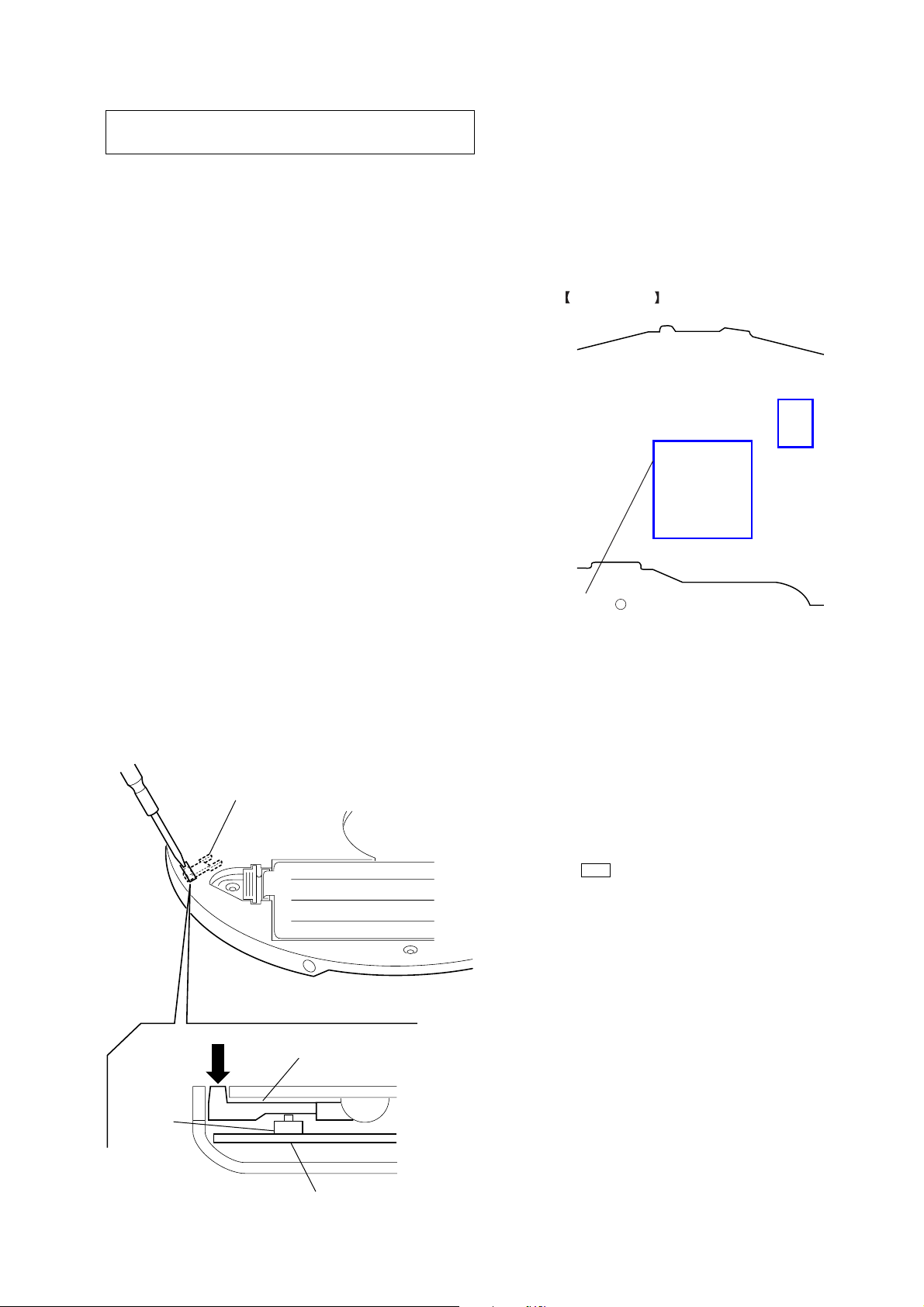
LASER DIODE AND FOCUS SEARCH OPERATION
CHECK
During normal operation of the equipment, emission of the laser
diode is prohibited unless the upper lid is closed while turning ON
the S820. (push switch type)
The following checking method for the laser diode is operable.
• Method:
Emission of the laser diode is visually checked.
1. Open the upper lid.
2. With a disc not set, turn on the S820 with a screwdr iver ha ving a
thin tip as shown in Fig.1.
3. Press the u button.
4. Observing the objective lens, check that the laser diode emits
light.
When the laser diode does not emit light, automatic power control
circuit or optical pickup is faulty.
In this operation, the objective lens will move up and down 4
times along with inward motion for the focus search.
S820
MAIN board
Fig. 1 Method to push the S820
3
D-NE1/NE9
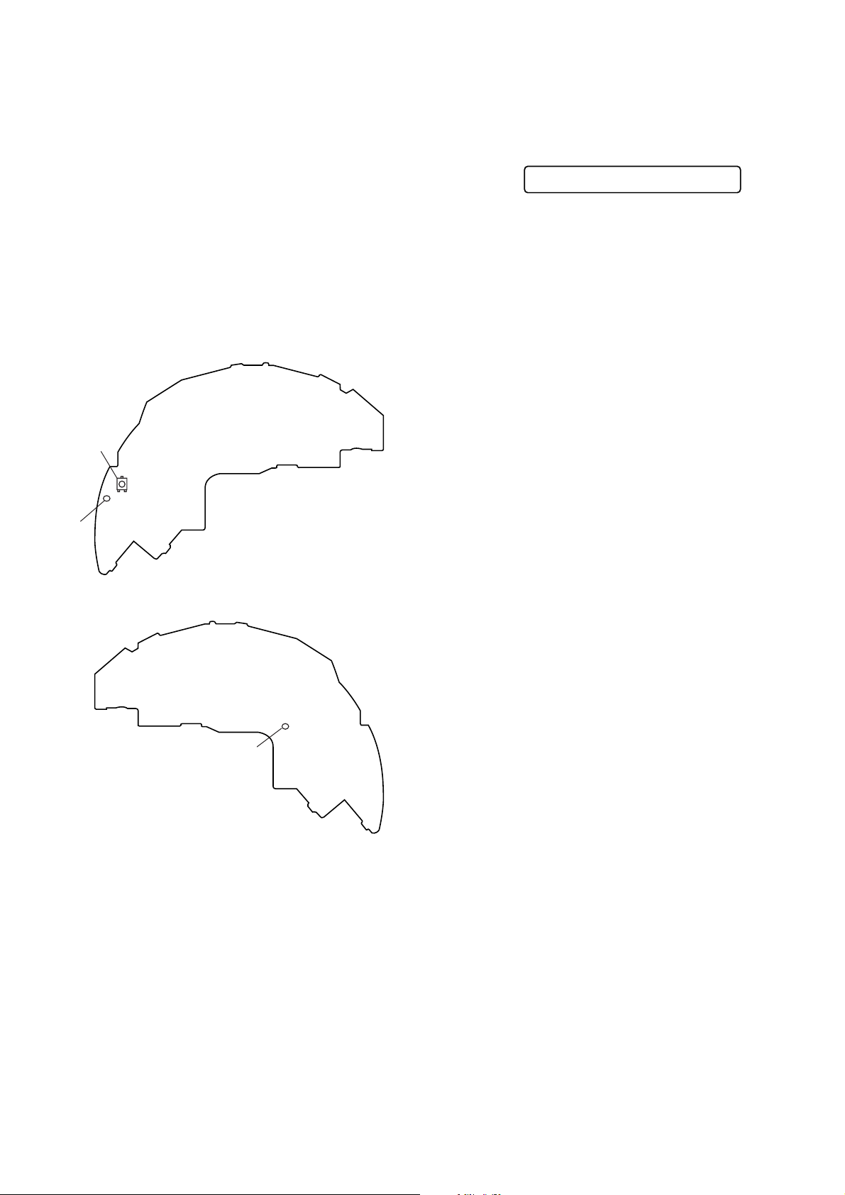
SERVICE MODE
The following confirmation can be performed when the Service
Mode is set.
1. How to set the Service Mode.
To set the Service Mode, the following method is available.
1) Confirm the set is not powered on.
2) Confirm the following settings.
OPEN/CLOSE detect switch (S820) ........ OFF
Solder Land (SL825) ................................ OPEN
[AVLS] switch (S821) ............................... NORM
[HOLD] switch (S810)............................... OFF
[G-PROTECTION] switch (S811) .............. 1
3) Short the solder land SL824 (TEST) on the MAIN board.
4) Turn on the main power.
MAIN BOARD (SIDE A)
SL820
(OPEN/CLOSE)
2. Operation when the Service Mode is set.
When the Service Mode becomes active, following messages are
displayed onthe remote control LCD.
Microcomputer
version display
1) Turn off the power.
2) Open the solder land SL824 (TEST) on the MAIN board.
Noto : The solder should be removed clean.
VF098I
SL825
(OPEN)
MAIN BOARD (SIDE B)
SL824
(TEST)
4
SECTION 2
GENERAL
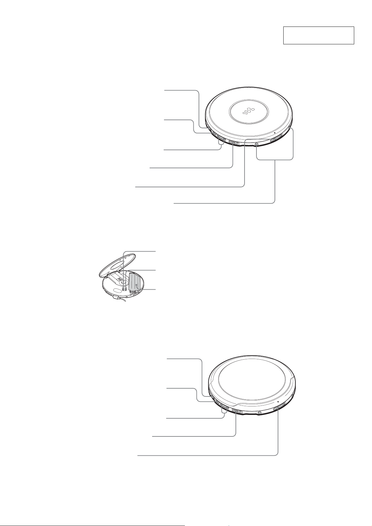
Locating the controls
CD player (front) (D-NE1)
1 Jog lever (u (play/pause)•
./> (AMS/search))
(pages 13, 14, 20 - 22)
2 x (stop) /CHARGE button•
CHARGE lamp
(pages 14, 25, 26, 28, 29)
3 VOL (volume) +*/– buttons
(page 14)
4 i (headphones) jack
(page 13)
5 OPEN switch
(page 13)
D-NE1/NE9
This section is extracted
from instruction manual.
6 Terminals for the charging stand
(pages 28, 34)
CD player (inside)
7 AVLS switch
(page 25)
8 G-PROTECTION switch
(page 23)
9 Battery compartment
(page 28, 30)
CD player (front) (D-NE9)
1 Jog lever (u (play/pause)•
./> (AMS/search))
(pages 13, 14, 20 - 22)
*The button has a tactile dot.
2 x (stop) /CHARGE button•
CHARGE lamp
(pages 14, 25, 26, 28, 29)
3 VOL (volume) +*/– buttons
(page 14)
4 i (headphones) jack
(page 13)
5 OPEN switch
(page 13)
*The button has a tactile dot.
5
D-NE1/NE9
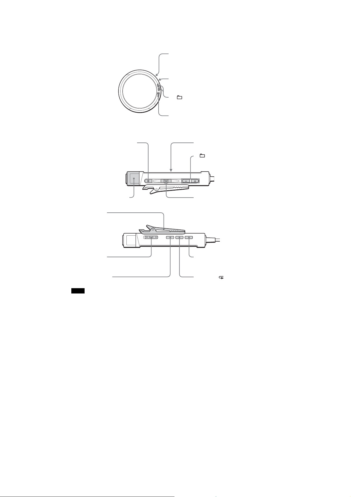
CD player (rear)
0 EXT BATT (external battery)/
DC IN 4.5 V (external power input)
jack (pages 13, 29, 31)
qa LINE OUT (OPTICAL) jack
(page 27)
qs +/– buttons
(pages 14, 22)
qd HOLD switch
(page 25)
Remote control
qf x (stop) button (pages 14, 26)
qg VOL (volume) +/– control
(page 14)
ql Clip (page 11)
w; HOLD switch
(page 25)
wa DISPLAY button
(pages 15, 23, 24)
Note
Use only the supplied remote control. You cannot operate this CD player with the remote control supplied with
other CD players.
qh Display
(pages 15, 18, 21 - 25)
qj +/– buttons
(pages 14, 22)
qk Jog lever (u (play/pause)•
ENT (enter)•
./> (AMS/search))
(pages 14, 18, 20 - 22)
ws SOUND button
(page 24)
wd P MODE/
(play mode/repeat) button
(pages 18 - 22, 26)
6
D-NE1/NE9
SECTION 3
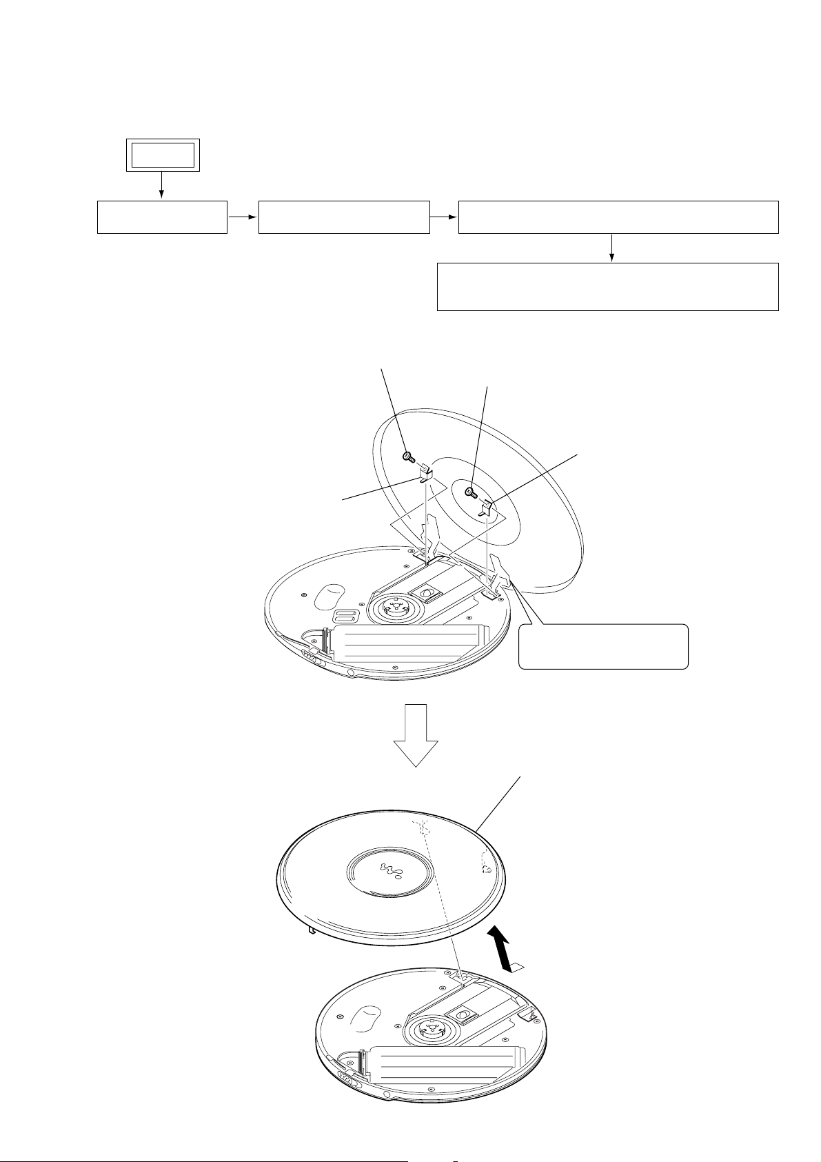
DISASSEMBLY
Note : Disassemble the unit in the order as shown below.
SET
UPPER LID SECTION CABINET (UPPER) SECTION MAIN BOARD, CD MECHANISM SECTION (CDM-3325ER2)
MOTOR ASSY (SPINDLE) (M901),MOTOR ASSY (SLED)(M902),
OPTICAL PICK-UP ASSY (DAX-25E)
Note : Follow the disassembly procedure in the numerical order given.
1
3-1. Upper Lid Section
tapping screw (B2)
3
tapping screw (B2)
2
guide (L)
4
guide (R)
The form of fulcrum plate
differs in the D-NE1 and D-NE9.
5
upper lid block assy
7
D-NE1/NE9
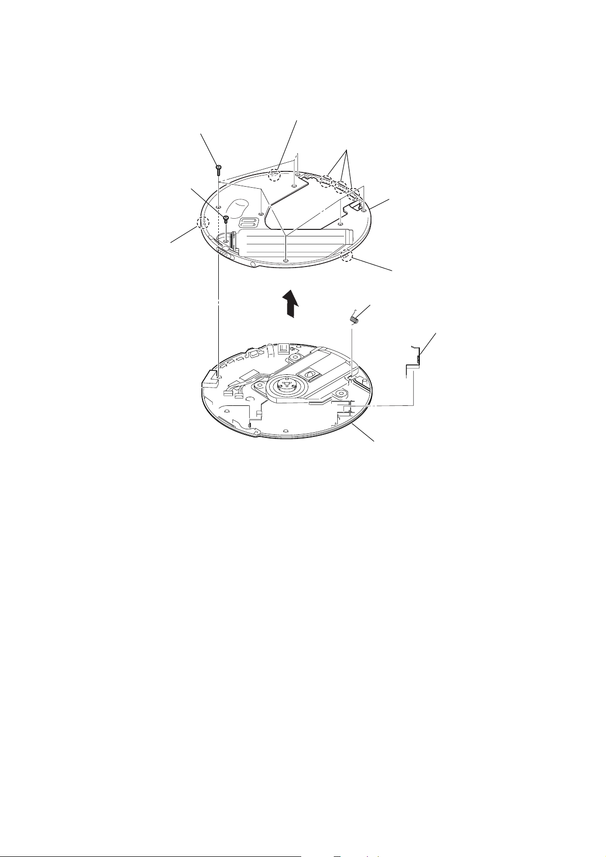
3-2. Cabinet (upper) Section
1
seven tapping screws (B2)
2
tapping screw (B2)
3
claw
4
claw
5
three claws
9
7
cabinet (upper) block assy
6
claw
spring (upper lid)
8
battery terminal board (relay)
cabinet (lower) block assy
8
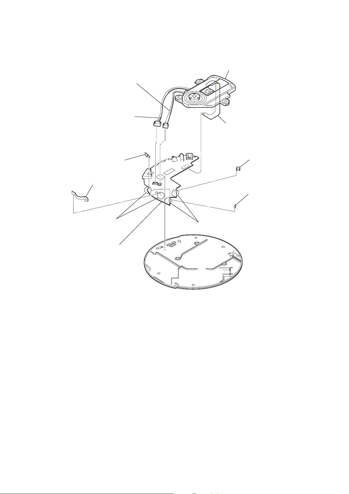
3-3. MAIN Board, CD Mechanism Section (CDM-3325ER2)
1
connector (2P)
(CN401)
2
connector (4P)
(CN402)
7
charge terminal board (+)
6
charge terminal board (-)
4
CD mechanism deck
(CDM-3325ER2)
3
flexible board
(CN601)
9
battery terminal board (+)
0
battery terminal board (-)
D-NE1/NE9
5
Remove two solders of the
MAIN board.
qa
MAIN board
8
Remove two solders of the
MAIN board.
9
D-NE1/NE9
p
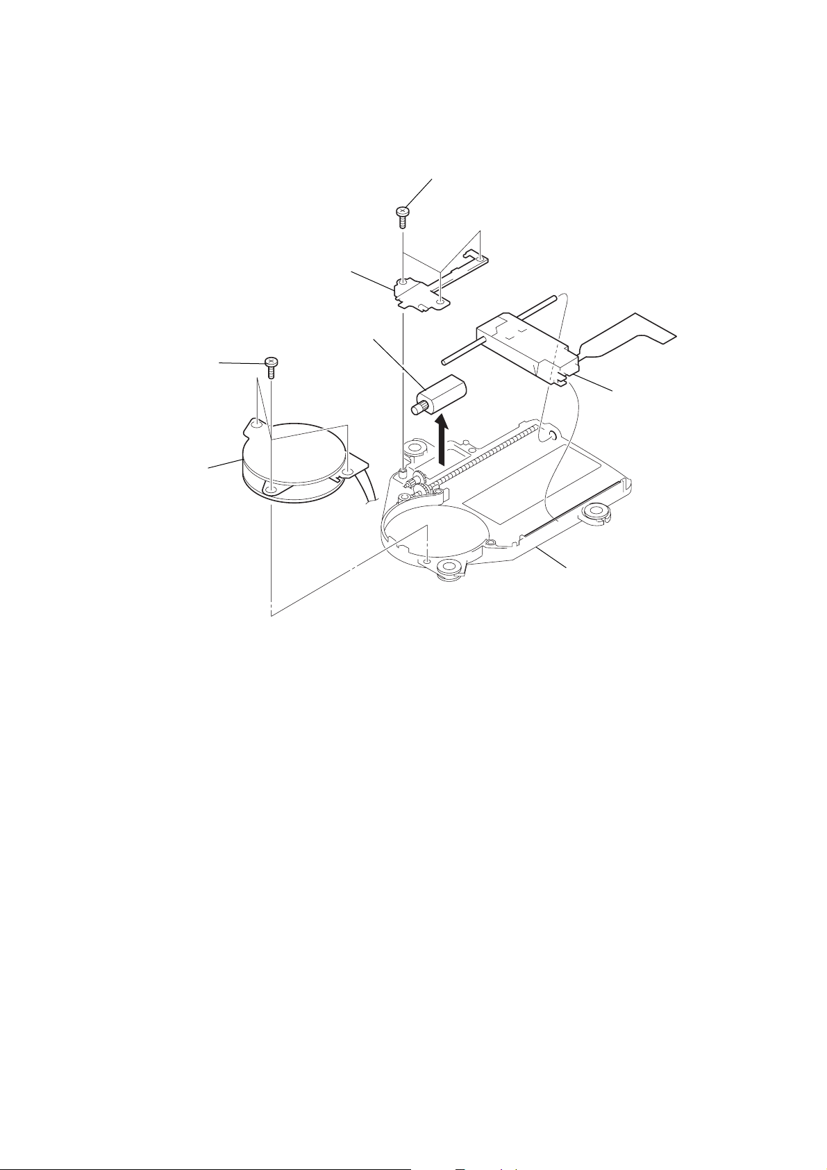
3-4. Motor Assy (Spindle)(M901), Motor Assy (Sled)(M902), Optical Pick-up Assy (DAX-25E)
1
three screws
(B1.7x4)
2
gear cover
3
motor assy
(sled) (M902)
5
three screws
(B1.7x4)
4
optical pick-u
(DAX-25E)
6
turn table motor assy
(spindle) (M901)
chassis
10
e
RF level
0.45 to 0.65 Vp-p
SECTION 4
ELECTRICAL CHECKING
D-NE1/NE9
The CD section adjustments are done automatically in this set.
In case of operation check, confirm that RF level.
Precautions for Check
1. Perform check in the order given.
2. Use YEDS-18 disc (Part No.: 3-702-101-01) unless otherwise
indicated.
3. Power supply voltage requirement : DC4.5 V in DC IN jack.
(J401)
VOLUME button : Minimum
AVLS switch : NORM
HOLD switch : OFF
G-PROTECTION switch : 1
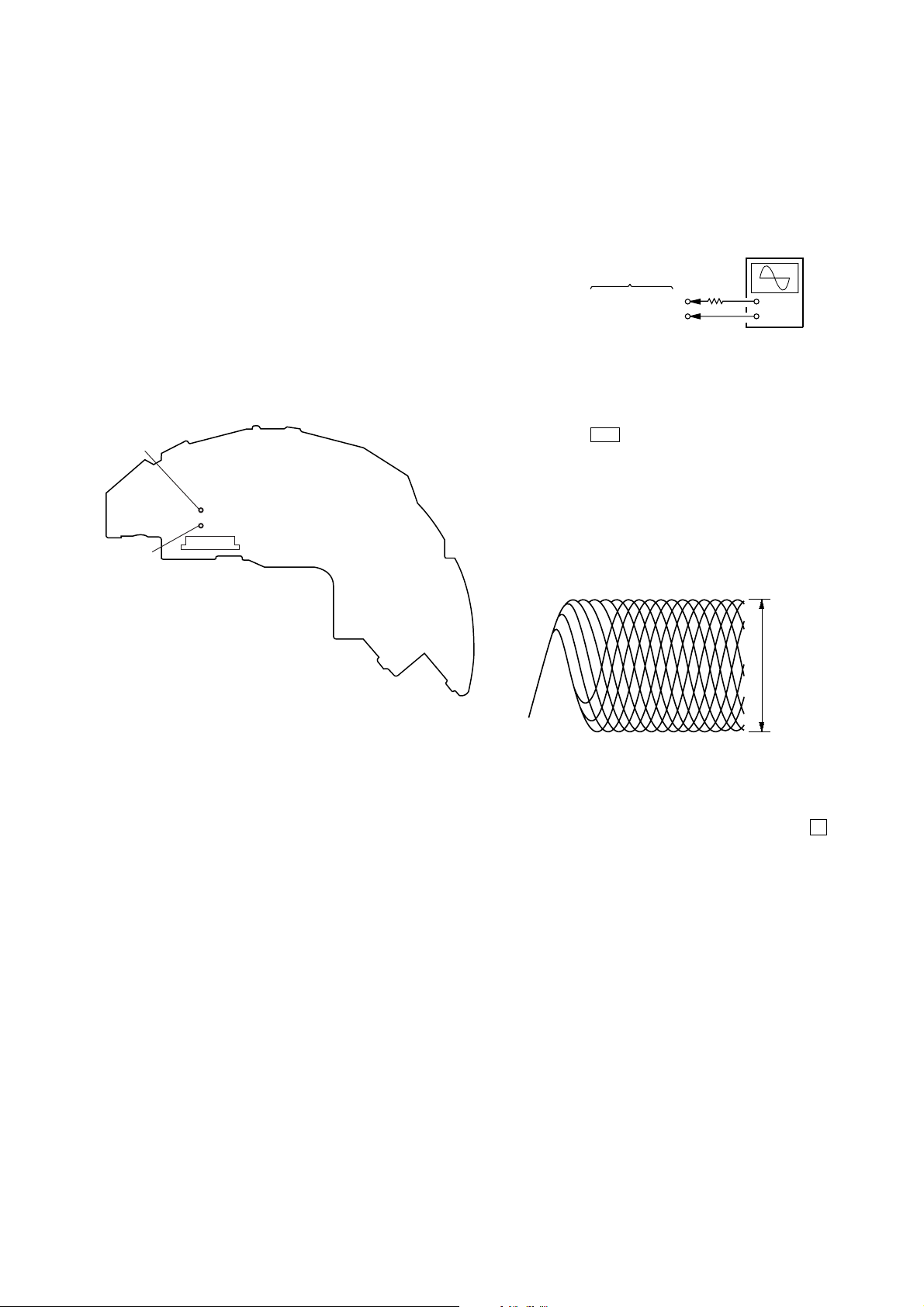
Checking Location:
– MAIN board (Side B) –
TP701
(AGND)
TP746
(RF)
CN601
RF Level Check
Condition:
• Hold the set in horizontal state.
Connection:
Oscilloscop
(AC range)
MAIN board
2 k
TP746 (RF)
TP701 (AGND)
Ω
+
–
Procedure:
1. Connect the oscilloscope to the test points TP746 (RF) and
TP701 (AGND) on the MAIN board.
2. Set a disc. (YEDS-18)
3. Press the u button.
4. Check the oscilloscope waveform is as shown below.
A good eye pattern means that the diamond shape (◊) in the
center of the waveform can be clearly distinguished.
RF Signal reference Waveform (Eye Pattern)
VOLT/DIV : 100 mV (With the 10:1 probe in use)
TIME/DIV : 500 ns
To watch the eye pattern, set the oscilloscope to AC range and
increase the vertical sensitivity of the oscilloscope for easy watching.
5. Stop revolving of the disc motor by pressing the x button.
11
 Loading...