

Sony DEJ-750 Service manual
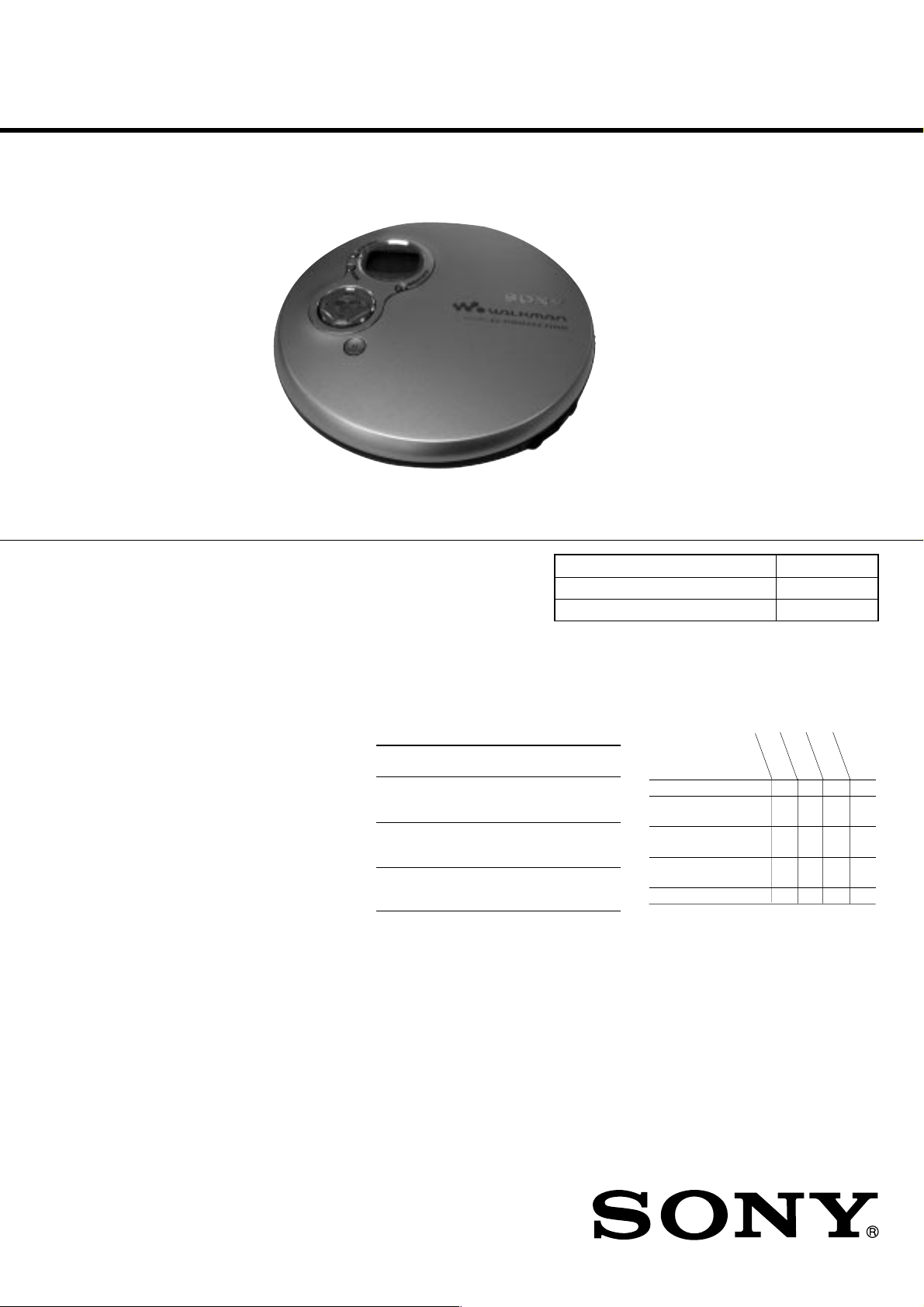
D-EJ750/EJ751/EJ753/EJ755/EJ756CK/EJ758CK
SERVICE MANUAL
Ver 1.0 2002.02
Photo : D-EJ755
US Model
D-EJ756CK/EJ758CK
Canadian Model
UK Model
D-EJ751/EJ755/EJ758CK
AEP Model
D-EJ750/EJ751/EJ753/EJ755/EJ758CK
Australian Model
E Model
D-EJ751/EJ758CK
Chinese Model
D-EJ751
Model Name Using Similar Mechanism D-E350
CD Mechanism Type CDM-3125ER
Optical Pick-up Type DAX-25E
System
Compact disc digital audio system
Laser diode properties
Material: GaAlAs
Wavelength : λ = 780 nm
Emission duration : Continuous
Laser output : Less than 44.6 µW
(This output is the value measured at a distance
of 200 mm from the objective lens surface on
the optical pick-up block with 7 mm aperture.)
D-A conversion
1-bit quartz time-axis control
Frequency response
20 - 20 000 Hz
Output (at 4.5 V input level)
Line output (stereo minijack)
Output level 0.7 V rms at 47 k
Recommended load impedance over 10 k
Headphones (stereo minijack)
Approx.5 mW + Approx. 5 mW at 16 Ω
(Approx. 0.5 mW + Approx. 0.5 mW at 16 Ω)*
*For the customers in France
Power requirements
For the area code of the model you
purchased, check the upper left side of the
bar code on the package.
• Two Sony NC-WMAA rechargeable
batteries: 2.4 V DC
• Sony NH-WM2AA rechargeable batteries:
2.4 V DC
• Two LR6 (size AA) batteries: 3 V DC
• AC power adaptor (DC IN 4.5 V jack):
US, CND, C&SA, MX model: 120 V, 60 Hz
AEP, FR, G, EE, E13 mode : 220 - 230 V, 50/60 Hz
UK model: 230 - 240 V, 50 Hz
AUS model: 240 V, 50 Hz
CH model: 220 V, 50 Hz
+
1
dB (measured by JEITA CP-307)
–2
SPECIFICATIONS
Battery life* (approx. hours)
(When you use the CD player on a flat and stable surface.)
Playing time varies depending on how the CD player is
used.
When using G-PROTECTION function
Two NC-WMAA 12 10
(charged for
about 3 hours**)
NH-WM2AA 25 22
(charged for
about 5 hours**)
Two Sony alkaline 48 38
batteries LR6(SG)
(produced in Japan)
* Measured value by the standard of JEITA (Japan
Electronics and Information Technology
Industries Association).
** Charging time varies depending on how the
rechargeable battery is used.
Operating temperature
5°C - 35°C (41°F - 95°F)
Dimensions (w/h/d) (excluding projecting
parts and controls)
Approx. 135.5 × 29.2 × 137.4 mm
(5 3 ⁄ 8 × 1 3 ⁄
Mass (excluding accessories)
Approx. 185 g (6.6 oz.)
Design and specifications are subject to change
without notice.
16
× 5
1
⁄ 2 in.)
on off
Accessories
Supplied accessories
For the area code of the location in which you
purchased the CD player, check the upper left
side of the bar code on the package.
AC power adaptor (1)
Headphones/earphones
with remote control (1)
Headphones/
earphones (1)
Rechargeable
batteries (2)
Battery carrying case (1)
* 1 Supplied with MX models
* 2 Not supplied with MX models
D-EJ756CK/EJ758CK
AC power adaptor (1)
Headphones/earphones (1)
Rotary commander (1)
Car battery cord (1)
Car connecting pack (1)
Velcro tape for the CD player (4)
Velcro tape for the rotary commander (2)
Hand strap (1)
D-EJ751
D-EJ750
–
–
aa
––
––
D-EJ755
D-EJ753
aaa
1
a
*
a
2
*
a
–
aa
aa
PORTABLE CD PLAYER
9-873-580-01
2002B0200-1
© 2002.02
Sony Corporation
Personal Audio Company
Pubulished by Sony Engineering Corporation
D-EJ750/EJ751/EJ753/EJ755/EJ756CK/EJ758CK
TABLE OF CONTENTS
• Abbreviation
AUS : Australian
FR : French
EE : East European
CND : Canadian
CH : Chinese
MX : Mexico
C&SA : Central and South America
E13 : AC220-230V area model
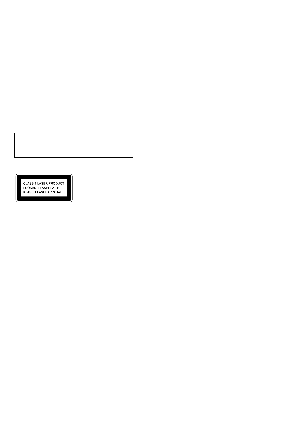
DANGER
Invisible laser radiation when open and interlock failed or defeated.
Avoid direct exposure to beam.
CAUTION
Use of controls or adjustments or performance of procedures other
than those specified herein may result in hazardous radiation
exposure.
Laser component in this product is capable of emitting
radiation exceeding the limit for Class 1.
This Compact Disc player is
classified as a CLASS 1 LASER
product.
The CLASS 1 LASER
PRODUCT label is located on
the rear exterior.
Flexible Circuit Board Repairing
• Keep the temperature of the soldering iron around 270°C during
repairing.
• Do not touch the soldering iron on the same conductor of the
circuit board (within 3 times).
• Be careful not to apply force on the conductor when soldering or
unsoldering.
Notes on chip component replacement
• Never reuse a disconnected chip component.
• Notice that the minus side of a tantalum capacitor may be dam-
aged by heat.
Specifications ............................................................................ 1
1. SERVICING NOTES................................................... 3
2. GENERAL
Locating the Controls......................................................... 3
3. DISASSEMBLY
3-1. Upper Lid Sub ASSY, Cabinet (Front) Sub ASSY..... 4
3-2. MD ASSY, Main Board .............................................. 5
3-3. “Motor ASSY, Turn Table (Spindle) (M901)”............ 5
3-4. “Motor ASSY (Sled) (M902)”,
Optical Pick-up (DAX-25E) ...................................... 6
4. ELECTRICAL ADJUSTMENS ............................... 7
5. DIAGRAMS
5-1. Explanation of IC Terminals....................................... 8
5-2. Block Diagram.......................................................... 13
5-3. Printed Wiring Boards .............................................. 14
5-4. Schematic Diagram –MAIN SECTION (1/3)– ....... 15
5-5. Schematic Diagram –MAIN SECTION (2/3)– ....... 16
5-6. Schematic Diagram –MAIN SECTION (3/3)– ....... 17
6. EXPLODED VIEWS
6-1. Upper Lid Section..................................................... 19
6-2. Cabinet Section......................................................... 20
6-3. Optical pick-up Section (CDM-3125ER) ................. 21
7. ELECTRICAL PARTS LIST................................... 22
SAFETY-RELATED COMPONENT WARNING!!
COMPONENTS IDENTIFIED BY MARK 0 OR DOTTED LINE
WITH MARK 0 ON THE SCHEMATIC DIAGRAMS AND IN THE
PARTS LIST ARE CRITICAL TO SAFE OPERATION.
REPLACE THESE COMPONENTS WITH SONY PARTS WHOSE
PART NUMBERS APPEAR AS SHOWN IN THIS MANUAL OR IN
SUPPLEMENTS PUBLISHED BY SONY.
ATTENTION AU COMPOSANT AYANT RAPPORT
LES COMPOSANTS IDENTIFIÉS P AR UNE MARQUE 0 SUR LES
DIAGRAMMES SCHÉMATIQUES ET LA LISTE DES PIÈCES
SONT CRITIQUES POUR LA SÉCURITÉ DE FONCTIONNEMENT .
NE REMPLACER CES COMPOSANTS QUE PAR DES PIÈCES
SONY DONT LES NUMÉROS SONT DONNÉS DANS CE MANUEL
OU DANS LES SUPPLÉMENTS PUBLIÉS PAR SONY.
À LA SÉCURITÉ!
2
D-EJ750/EJ751/EJ753/EJ755/EJ756CK/EJ758CK
SECTION 1
SERVICING NOTES
NOTES ON HANDLING THE OPTICAL PICK-UP BLOCK OR
BASE UNIT
The laser diode in the optical pick-up block may suffer electrostatic
breakdown because of the potential difference generated by the charged
electrostatic load, etc. on clothing and the human body. During repair,
pay attention to electrostatic breakdown and also use the procedure in
the printed matter which is included in the repair parts.
The flexible board is easily damaged and should be handled with care.
NOTES ON LASER DIODE EMISSION CHECK
The laser beam on this model is concentrated so as to be focused on the
disc reflective surface by the objective lens in the optical pick-up block.
Therefore, when checking the laser diode emission, observe from more
than 30cm away from the objective lens.
Before Replacing the Optical pick-up Block
Please be sure to check thoroughly the parameters as per the “Optical
pick-up Block Checking Procedure” (Part No. : 9-960-027-11) issued
separately before replacing the optical Pick-up block.
Note and specifications required to check are given below.
• FOK output : IC601 yg pin
When checking FOK, remove the lead wire to disc motor.
• RF signal P-to-P value : 0.45 to 0.65Vp-p
Laser Diode Checking Methods
During normal operation of the equipment, emission of the laser diode
is prohibited unless the upper panel is closed while turning ON the S801
(push switch type).
The following two checking methods for the laser diode are operable.
Method :
Emission of the laser diode is visually checked.
1. Open the upper lid.
2. Push the S801 as shown in Fig. 1 .
3. Check the object lens for confirming normal emission of the laser
diode. If not emitting, there is a trouble in the automatic power
control circuit or the optical pick-up. During normal operation, the
laser diode is turned ON about 2.5 seconds for focus searching.
S801
LOCA TING THE CONTROLS
CD player (front)
1 PLAY MODE
button
2 SOUND button
3
VOL (volume) +*
4 'm (AMS/
search) button
5 VOL (volume) –
button
6 X (pause) button
7 x (stop)/CHG (charge)
button
8qjN* (play)/>
(AMS/search) button
SECTION 2
GENERAL
Fig.1 Method to push S801
This section is extracted from
instruction manual.
9 DC IN 4.5 V (external
power input) jack
0 Strap holes
qa Display
qs REPEAT/ENTER
button
qd HOLD switch
qf OPEN switch
qg LINE OUT
qh i (headphones)
CD player (inside)
G-PROTECTION
switch
*The button has a tactile dot.
qk Battery compartment
3
D-EJ750/EJ751/EJ753/EJ755/EJ756CK/EJ758CK
SECTION 3
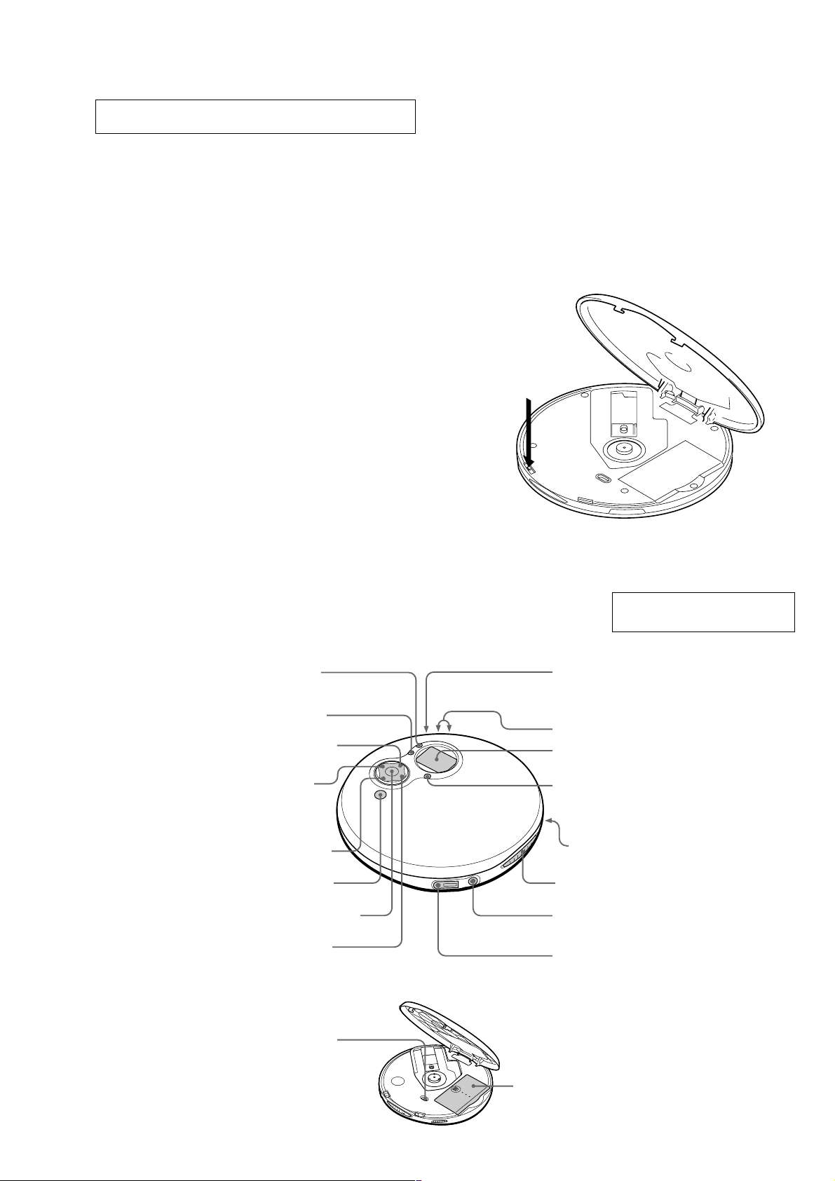
DISASSEMBLY
z
The equipment can be removed using the following procedure.
MD ASSY “Motor ASSY, turn table (spindle) (M901)”, Optical pick-up (DAX-25E),
“Motor ASSY (Sled) (M902)”
Set
Upper lid sub ASSY,
Cabinet (front) sub ASSY
Main board
Note : Follow the disassembly procedure in the numerical order given.
3-1. UPPER LID SUB ASSY, CABINET (FRONT) SUB ASSY
Upper lid sub ASSY
6 Switch unit
flexible board
4
7 Six screws (B2)
5 Connector cover
Cabinet (front)
sub ASSY
1 Open
8 Claw
3 Spring (full
open), left
2 Spring (full
open), right
9
8 Claw
• CAUTION DURING ASSSEMBLY
2
CN801
5
6 Spring
(full open),
left
3
1 Switch unit
flexible board
2
8 Claw
• "SPRING FULL OPEN" REMOVAL
1
2
Cabinet (rear) sub ASSY
4
3 Spring (full open), right
• "SPRING FULL OPEN" INSTALL
Insert the point
1
2Push in
1
4
Y
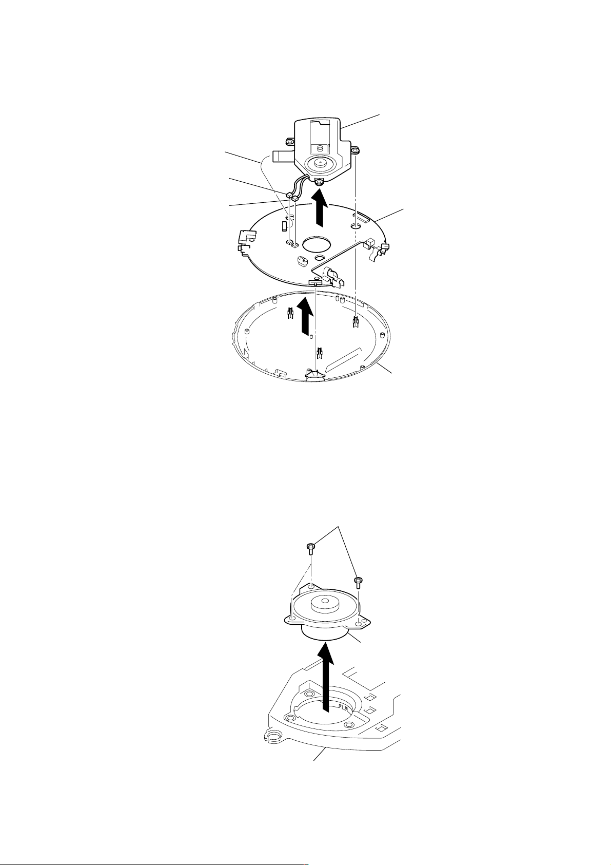
3-2. MD ASSY, MAIN BOARD
e
1 CN501
2 CN502 (black)
D-EJ750/EJ751/EJ753/EJ755/EJ756CK/EJ758CK
MD ASSY
3 CN503 (white)
3-3. “MO TOR ASSY , TURN T ABLE
(SPINDLE) (M901)”
Main board
Cabinet (rear) sub ASS
1 Screws
(B1.7x5)
Motor ASSY, Turn tabl
(Spindle) (M901)
2
Chassis
5
D-EJ750/EJ751/EJ753/EJ755/EJ756CK/EJ758CK
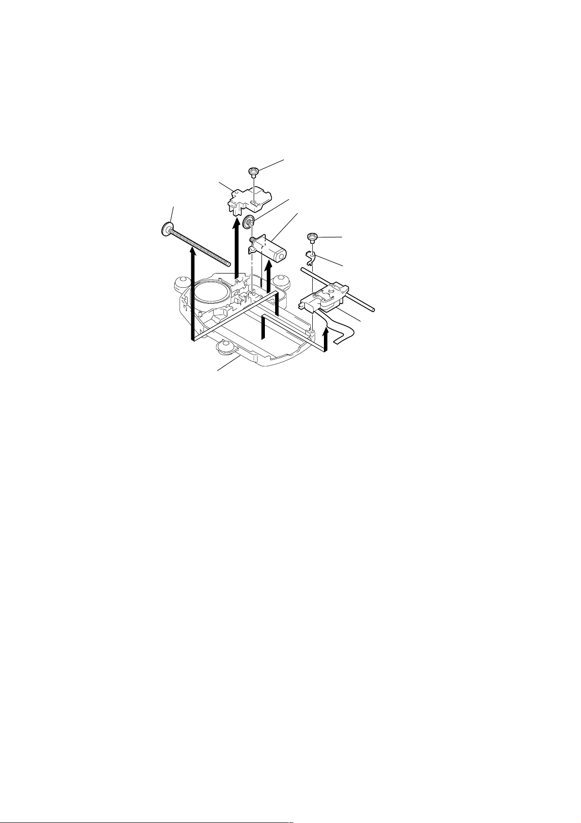
3-4. “MOTOR ASSY (SLED) (M902)”,
OPTICAL PICK-UP (DAX-25E)
1 Screw (B 1.7x5)
Cover, Gear
Screw ASSY, Feed
5
Chassis
2
Gear B
Motor ASSY (Sled) (M902)
3
6
4 Screw
(P 1.4x3.5)
Bracket (Shaft)
Optical pick-up
(DAX-25E)
6
D-EJ750/EJ751/EJ753/EJ755/EJ756CK/EJ758CK
C412
1
3
4
5
R6
C601
IC601
L602
L409
R408
R627
L601
D461
C604
C603
C602
R601
C630
C631
C629
C632
C633
C634
C635
R631
TP630
(RF)
R632
R633
R634
R635
R636
R637
R638
R639
R640
R624
C620
C615
C616
C617
C618
R618
R619
R620
R621
R622
R623
C619
IC402
C60
L302
R463
C461
C462
R461
R462
C607
C608
C626
C610
C621
C622
R625
R616
C613
C627
R1
R615
L605
R432
C624
R317
R433
L606
Q409
120
31
60
61
90
91
RF level
0.45 to 0.65 Vp-p
VOLT/DIV : 100 mV (With the 10 : 1 probe in use)
TIME/DIV : 500ns
SECTION 4
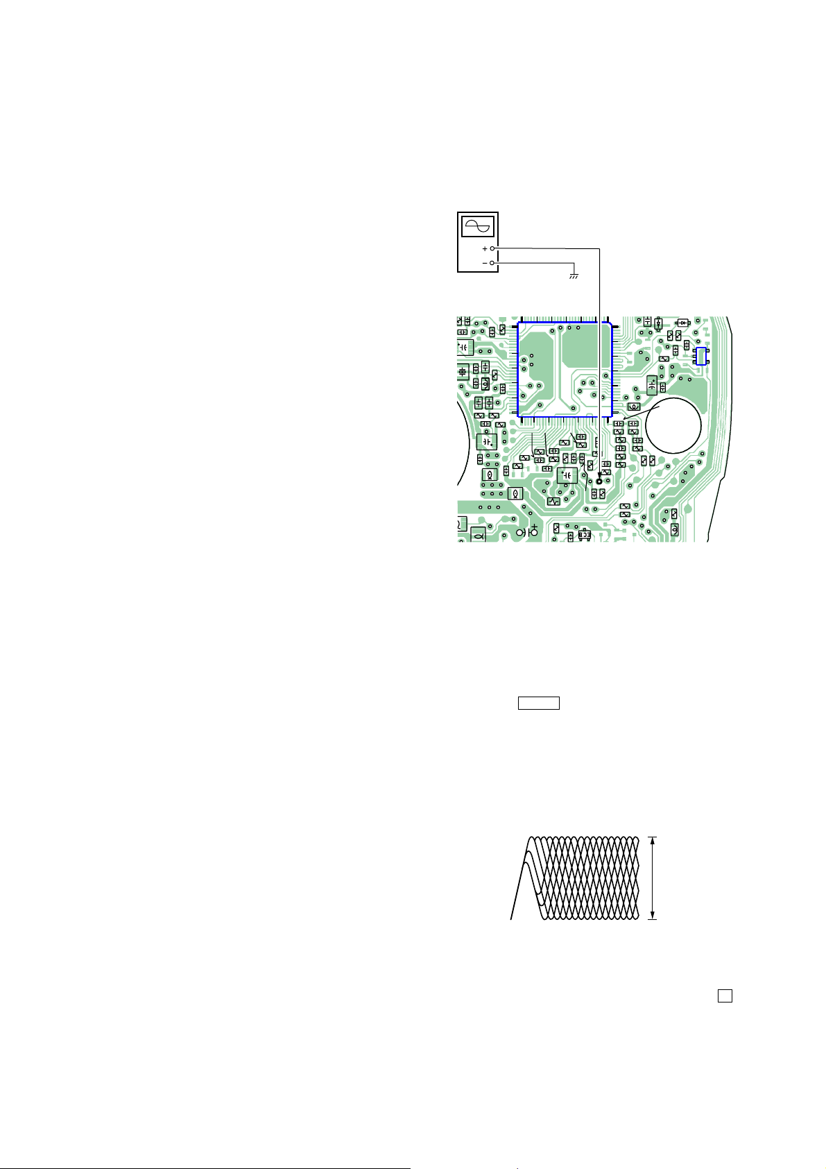
ELECTRICAL ADJUSTMENTS
The CD section adjustments are done automatically in this set.
Precautions for Check
1. Perform check in the order given.
2. Use YEDS-18 disc (Part No.: 3-702-101-01) unless otherwise
indicated.
3. Power supply voltage requirement :DC4.5 V in DC IN jack.
(J401)
VOLUME button : Minimum
HOLD switch : OFF
Focus bias Check
Condition:
• Hold the set in horizontal state.
Connection:
oscilloscope
(AC range)
TP630(RF)
[MAIN BOARD] (SIDE A)
Procedure:
1. Connect the oscilloscope to the test point TP630(RF) on the
MAIN board.
2. Set a disc. (YEDS-18)
3. Press the >B button.
4. Check the oscilloscope waveform is as shown below.
A good eye pattern means that the diamond shape (◊) in the center of the waveform can be clearly distinguished.
RF Signal reference Waveform (Eye Pattern)
To watch the eye pattern, set the oscilloscope to AC range and
increase the vertical sensitivity of the oscilloscope for easy
watch-ing.
5. Stop revolving of the disc motor by pressing the x button.
7

D-EJ750/EJ751/EJ753/EJ755/EJ756CK/EJ758CK
SECTION 5
DIAGRAMS
5-1. EXPLANATION OF IC TERMINALS
IC601 (SYSTEM CONTROL) CXD3029R (DSP IC)
Pin No. Pin name I/O Description
1 XRAM O DRAM low address strobe signal outut.
2 XWE O DRAM data input enable signal output.
3 to 6 D0 to 3 I/O DRAM data bus 0 to 3.
7 DCLK O Not used (OPEN).
8 DCKE O Not used (OPEN).
9 XCAS O DRAM column address storobe signal output.
10 WFCK O Not used (OPEN).
11 to 13 A7 to 9 O DRAM address 7 to 9.
14 DVss – Ground terminal for DRAM interface.
15 to 17 A4 to 6 O DRAM addres 4 to 6.
18 XRDE I/O Not used (OPEN).
19 VDD0 – Power supply for digital.
20 CLOCK I Serial data transfer clock input.
21 SDTO I Serial data input.
22 SENS O SENS output.
23 XLAT I Latch input.
24 XSOE I CPU serial data output enable signal input.
25 SYSM I Mute input. “H” : MUTE
26 WDCK O Word clock output.
27 SCOR O SCOR output.
28 XRST I Reset terminal.
29 PWMI I Spindle moter external contorol input.
30 XQOK I/O Not used (OPEN).
31 XWER I/O DRAM write enable signal input.
32 R4M O System clock output.
33 Vss0 – Digital ground terminal.
34 SQCK I Clock input for SQSO read out.
35 SCLK I Clock input for SENS serial date read out.
36 SQSO O Not used (OPEN).
37 XEMP O Not used (OPEN).
38 XWIH O Not used (OPEN).
39 SBSO O Not used (OPEN).
40 EXCK I Not used (Fixed at “L”).
41 XTSL I Not used (Fixed at “L”).
42 HVss – Ground terminal for headphones.
43 HPL O Headphone output (L-CH).
44 HPR O Headphone output (R-CH)..
45 HVDD – Power supply terminal for headphones.
46 XVDD – Power supply terminal for master clock.
47 XTAI I Master clock input.
48 XTAO O Master clock output.
49 XVss – Ground terminal for master clock.
50 AVDD1 – Power supply terminal for analog.
51 AOUT1 O Line out (L-CH).
52 VREFL O VREF terminal (L-CH).
53 AVss1 – Ground terminal for analog.
54 AVss2 – Ground terminal for analog.
8
D-EJ750/EJ751/EJ753/EJ755/EJ756CK/EJ758CK
Pin No. Pin name I/O Description
55 VREFR O VREF terminal(R-CH).
56 AOUT2 O Line out.
57 AVDD2 – Power supply terminal for analog.
58 TEST1 I Not used (Fixed at “L”).
59 TEST I Not used (Fixed at “L”)..
60 Vss1 – Not used (Fixed at “L”).
61 LRMU O OR output of L-CH/R-CH detection flag (AND output) and system flag.
62 DOUT O Not used (OPEN)
63 ATSK I/O Not used (OPEN).
64 DFCT I/O Not used (OPEN).
65 FOK I/O Focus OK signal I/O teminal.
66 MIRR I/O Not used (OPEN).
67 COUT I/O Not used (OPEN).
68 C2PO O Not used (OPEN).
69 GFS O Not used (OPEN).
70 XUGF O Not used (OPEN).
71 XPCK O Not used (OPEN).
72 VDD1 – Power supply terminal for digital.
73 PCO O Charge pump output for master PLL.
74 FILI I Filter input for master PLL.
75 FILO O Filter output for master PLL.
76 CLTV I VC01 contorol voltage input.
77 VCTL I VC02 contorol voltage input for wide range EFM PLL.
78 VPCO O Charge pump output for wide range EFM PLL.
79 AVDD 3 – Ground terminal for analog.
80 ASYO O EMF fullswing output.
81 ASYI I Asymmetric comparate voltage input.
82 BIAS I Asymmetric circuit current constrant input.
83 AVDD3 – Power supply terminal for analog.
84 RFAC I EFM signal input.
85 AVDD0 – Power supply terminal for analog.
86 IGEN I Current constant input for OP amplifier.
87 AVss0 – Ground terminal for analog.
88 RFDC I RF signal input.
89 CE I E signal input.
90 TE I F signal input.
91 SE I B signal input.
92 FE I A signal input.
93 VC I Center voltage input.
94 Vss2 – Digital ground terminal.
95 FRDR O Focus drive output.
96 FFDR O Focus drive output.
97 TRDR O Traking drive output.
98 TFDR O Traking drive output.
99 SRDR O Sled drive output.
100 SFDR O Sled drive output.
101 SSTP I Most inside disc detection signal input.
102 MDS O Spindle drive output.
103 MDP O Servo contorol output for spindle moter.
104 C176 O 176.44kHz output.
9
 Loading...