

Sony DEJ-620 Service manual
D-E666/EJ620/EJ621/EJ622/
EJ623/EJ625/EJ626CK
SERVICE MANUAL
Ver 1.4 2001.11
with SUPPLEMENT-1
(9-873-048-81)
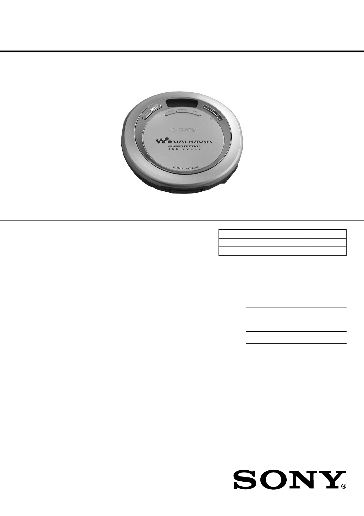
Photo : D-EJ620
US Model
D-EJ621/EJ622/EJ625/EJ626CK
Canadian Model
UK Model
E Model
Australian Model
D-EJ621/EJ625/EJ626CK
AEP Model
D-EJ620/EJ621/EJ623/EJ625/EJ626CK
Chinese Model
D-EJ621/EJ625
Tourist Model
D-E666
Model Name Using Similar Mechanism D-EJ711
CD Mechanism Type CDM-3123EBA
Optical Pick-up Type DAX-23E
System
Compact disc digital audio system
Laser diode properties
Material: GaAIAs
Wavelength : λ= 780 nm
Emission duration: Continuous
Laser output : Less than 44.6 µW
(This output is the value measured at a distance
of 200 mm from the objective lens surface on
the optical pick-up block with 7 mm aperture. )
D-A conversion
1-bit quartz time-axis control
Frequency response
20 - 20,000 Hz+1 dB (measured by EIAJ CP-
307)
Output (at 4.5 V input level)
Line output (stereo minijack)
Output level 0.7 V rms at 47 kilohms
Recommended load impedance over 10
kilohms
Headphones (stereo minijack)
Approx. 5 mW + Approx. 5 mW at 16 Ω
(Approx. 1 mW + Approx. 1 mW at 16 Ω)*
*For the customers in France
-2
SPECIFICATIONS
Power requirements
For the area code of the model you purchased,
check the upper left side of the bar code on the
package.
• Two Sony NC-WMAA rechargeable
batteries: 2.4 V DC,
• Sony NH-WM2AA rechargeable batteries:
2.4 V DC,
• Two LR6 (size AA) batteries: 3 V DC
• AC power adaptor (DC IN 4.5 V jack):
US, Canadian, C&SA, MX model:
120 V, 60 Hz
AEP, FR, G, EE, E13, G model:
220 - 230 V, 50/60 Hz
UK, 3AEP7 model: 230 - 240 V, 50 Hz
AUS model: 240 V, 50 Hz
JEW, E33 model: 100 - 240 V, 50/60 Hz
HK model: 220 V, 50/60 Hz
AR, CH model: 220 V, 50 Hz
• Sony DCC-E345 car battery cord for use on
car battery : 4.5V DC
Battery life* (approx. hours)
(When you use the CD player on a flat and
stable surface.)
Playing time varies depending on how the CD
player is used.
When using G-PROTECTION function
on off
Tow NC-WMAA 10 8
(charged for about 3 hours**)
NH-WM2AA 21 18
(charged for about 5 hours**)
Two Sony alkaline batteries 36 32
LR6 (SG)
* Measured value by the standard of EIAJ
(Electronic Industries Association of Japan).
** Charging time varies depending on how the
rechargeable battery is used.
Operating temperature
5°C - 35°C (41°F - 95°F)
– Continued on page 2 –
9-873-048-15
2001K0200-1
© 2001.11
PORTABLE CD PLAYER
Sony Corporation
Personal Audio Company
Published by Sony Engineering Corporation
D-E666/EJ620/EJ621/EJ622/EJ623/EJ625/EJ626CK
Dimensions (w/h/d) (excluding projecting
parts and controls)
Approx. 131.6 x 29.5 x 135.5 mm
( 51/4 x 13/16 x 53/8 in.)
Mass (excluding accessories)
Approx. 191 g (6.8 oz)
Supplied accessories
For the area code of the location in which you
purchased the CD player, check the upper left side
of the bar code on the package.
D-EJ621/EJ622
D-EJ620
AC power adaptor (1) –
Headphones/earphones –a*
with remote control (1)
Headphones/
earphones (1)
Rechargeable ––
batteries (2)
Battery carrying case (1) ––
AC plug adaptor (1)
Hand strap (1)
*1Supplied with AR and MX models
2
*
Not supplied with AR and MX models
3
*
Supplied with E33 and JEW models
4
Supplied with AEP, G, UK, FR and EE
*
models
D-EJ626CK
AC power adaptor (1)
Headphones/earphones (1)
Rotary commander (1)*
Rotary commander mounting kit (1)*
Car battery cord (1)
Car connecting pack (1)
Velcro tape (2)
Spiral tube (1)
AC plug adaptor (1)*
Hand strap (1)*
3
aa
–––
aa
1
2
D-E666/EJ625
D-EJ623
aaa
1
–
2
*
a
aa
aa
4
*
aa
1
TABLE OF CONTENTS
Specifications ............................................................................ 1
1. SERVICING NOTES ................................................... 3
2. GENERAL
Locating the Controls......................................................... 4
3. DISASSEMBLY
3-1. Cabinet (Rear) Sub ASSY,
Cabinet (Front), Main Board....................................... 6
3-2. MD ASSY................................................................... 6
3-3. “Motor ASSY, Turn Table (Spindle) (M901)”............ 7
3-4. “Motor ASSY (Sled) (M902)”,
Optical Pick-up (DAX-23E) ...................................... 7
3-5. “Lid, Upper”, Switch Unit .......................................... 7
a
4. ELECTRICAL ADJUSTMENTS ............................. 8
–
5. DIAGRAMS
5-1. Explanation of IC Terminals....................................... 9
5-2. Block Diagram...........................................................11
5-3. Printed Wiring Boards – Main Section (Side A) – ... 12
3
a
*
4
*
5-4. Printed Wiring Boards – Main Section (Side B) – ... 13
5-5. Schematic Diagram – Main Section (1/2) – ............. 14
5-6. Schematic Diagram – Main Section (2/2) – ............. 15
6. EXPLODED VIEWS
6-1. Cabinet Section......................................................... 18
6-2. Optical pick-up Section (CDM-3123EBA) .............. 21
7. ELECTRICAL PARTS LIST ................................... 22
*1Supplied with Canadian, AEP, UK and G models
*2Supplied with E33 model
*3Supplied with AEP, UK and G models
Design and specifications are subject to change without notice.
• Abbreviation
AUS : Australian
FR : French HK : Hong Kong
AR : Argentina JEW : Tourist
G : German EE : East European
CH : Chinese
C&SA : Central and South America
E13 : AC220-230V area model
E33 : AC100-240V area model
3AEP7: UK
2
D-E666/EJ620/EJ621/EJ622/EJ623/EJ625/EJ626CK
S801
DANGER
Invisible laser radiation when open and interlock failed or defeated.
Avoid direct exposure to beam.
CAUTION
Use of controls or adjustments or performance of procedures other
than those specified herein may result in hazardous radiation
exposure.
Flexible Circuit Board Repairing
• Keep the temperature of the soldering iron around 270°C during
repairing.
• Do not touch the soldering iron on the same conductor of the
circuit board (within 3 times).
• Be careful not to apply force on the conductor when soldering or
unsoldering.
Notes on chip component replacement
• Never reuse a disconnected chip component.
• Notice that the minus side of a tantalum capacitor may be dam-
aged by heat.
SAFETY-RELATED COMPONENT WARNING!!
COMPONENTS IDENTIFIED BY MARK 0 OR DOTTED LINE
WITH MARK 0 ON THE SCHEMATIC DIAGRAMS AND IN THE
PARTS LIST ARE CRITICAL TO SAFE OPERATION.
REPLACE THESE COMPONENTS WITH SONY PARTS WHOSE
P ART NUMBERS APPEAR AS SHOWN IN THIS MANUAL OR IN
SUPPLEMENTS PUBLISHED BY SONY.
ATTENTION AU COMPOSANT AYANT RAPPORT
À LA SÉCURITÉ!
LES COMPOSANTS IDENTIFIÉS P AR UNE MARQUE 0 SUR LES
DIAGRAMMES SCHÉMATIQUES ET LA LISTE DES PIÈCES
SONT CRITIQUES POUR LA SÉCURITÉ DE FONCTIONNEMENT .
NE REMPLACER CES COMPOSANTS QUE PAR DES PIÈCES
SONY DONT LES NUMÉROS SONT DONNÉS DANS CE MANUEL
OU DANS LES SUPPLÉMENTS PUBLIÉS PAR SONY.
SECTION 1
SERVICING NOTES
NOTES ON HANDLING THE OPTICAL PICK-UP BLOCK OR
BASE UNIT
The laser diode in the optical pick-up block may suffer electrostatic
breakdown because of the potential difference generated by the charged
electrostatic load, etc. on clothing and the human body. During repair,
pay attention to electrostatic breakdown and also use the procedure in
the printed matter which is included in the repair parts.
The flexible board is easily damaged and should be handled with care.
NOTES ON LASER DIODE EMISSION CHECK
The laser beam on this model is concentrated so as to be focused on the
disc reflective surface by the objective lens in the optical pick-up block.
Therefore, when checking the laser diode emission, observe from more
than 30cm away from the objective lens.
Before Replacing the Optical pick-up Block
Please be sure to check thoroughly the parameters as per the “Optical
pick-up Block Checking Procedure” (Part No. : 9-960-027-11) issued
separately before replacing the optical Pick-up block.
Note and specifications required to check are given below.
• FOK output : IC601 eg pin
When checking FOK, remove the lead wire to disc motor.
• RF signal P-to-P value : 0.4 to 0.65Vp-p (Except US model)
: 0.35 to 0.65Vp-p (US model)
Laser Diode Checking Methods
During normal operation of the equipment, emission of the laser diode
is prohibited unless the upper panel is closed while turning ON the S801
(push switch type).
The following two checking methods for the laser diode are operable.
Method :
Emission of the laser diode is visually checked.
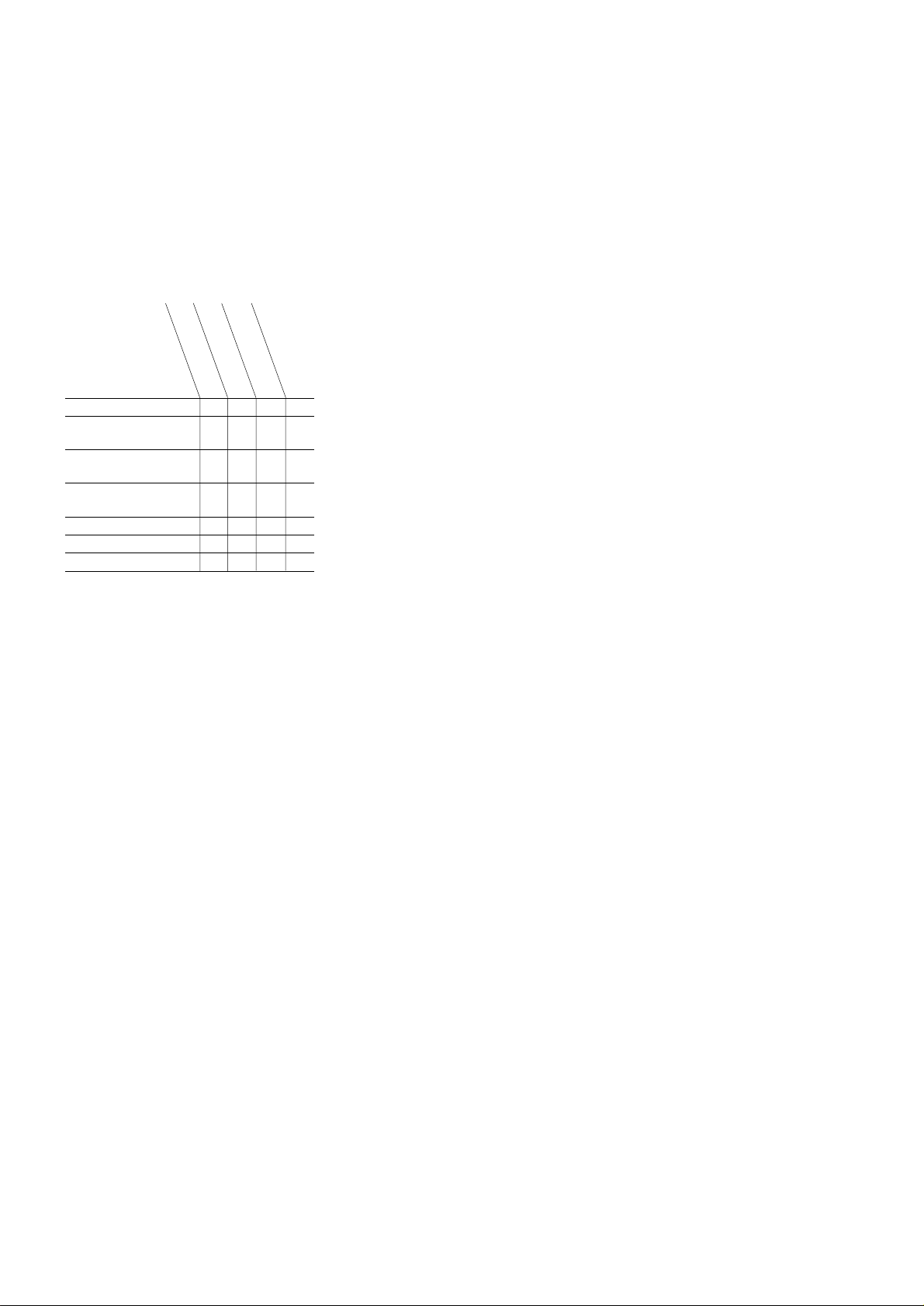
1. Open the upper lid.
2. Push the S801 as shown in Fig. 1 .
3. Check the object lens for confirming normal emission of the laser
diode. If not emitting, there is a trouble in the automatic power
control circuit or the optical pick-up. During normal operation, the
laser diode is turned ON about 2.5 seconds for focus searching.
Fig.1 Method to push S801
3
D-E666/EJ620/EJ621/EJ622/EJ623/EJ625/EJ626CK
SECTION 2
GENERAL
LOCA TING THE CONTROLS
CD player (front)
This section is extracted from
instruction manual.
1 Display
2 PLAY MODE
button
3 ./>
(AMS/search)
buttons
4 LINE OUT
5 HOLD switch
6 VOLUME +/–
buttons
7 u (play/pause)
button
8 DC IN 4.5 V (external
power input) jack
Strap holes
9
q; x (stop)/CHG (charge)
button
qa SOUND button
qs REPEAT/ENTER
button
qd i (headphones) jack
qf OPEN switch
CD player (inside)
qg G-PROTECTION
switch
4

CD player (rear)
D-E666/EJ620/EJ621/EJ622/EJ623/EJ625/EJ626CK
qh AVLS switch
qj Battery
compartment
Remote control
qk x (stop) button
ql VOL (volume)
+/– button
(for the models supplied with the remote control)
w; N(play)•>
(AMS/search) button
wa HOLD switch
ws .(AMS/search)
button
5
D-E666/EJ620/EJ621/EJ622/EJ623/EJ625/EJ626CK
d
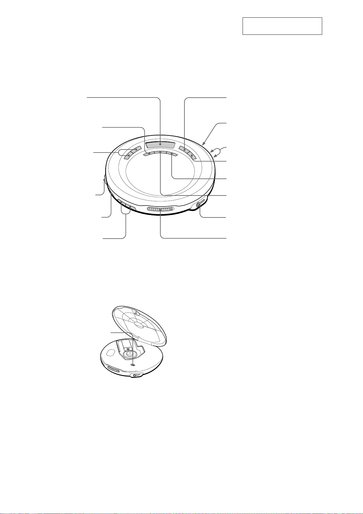
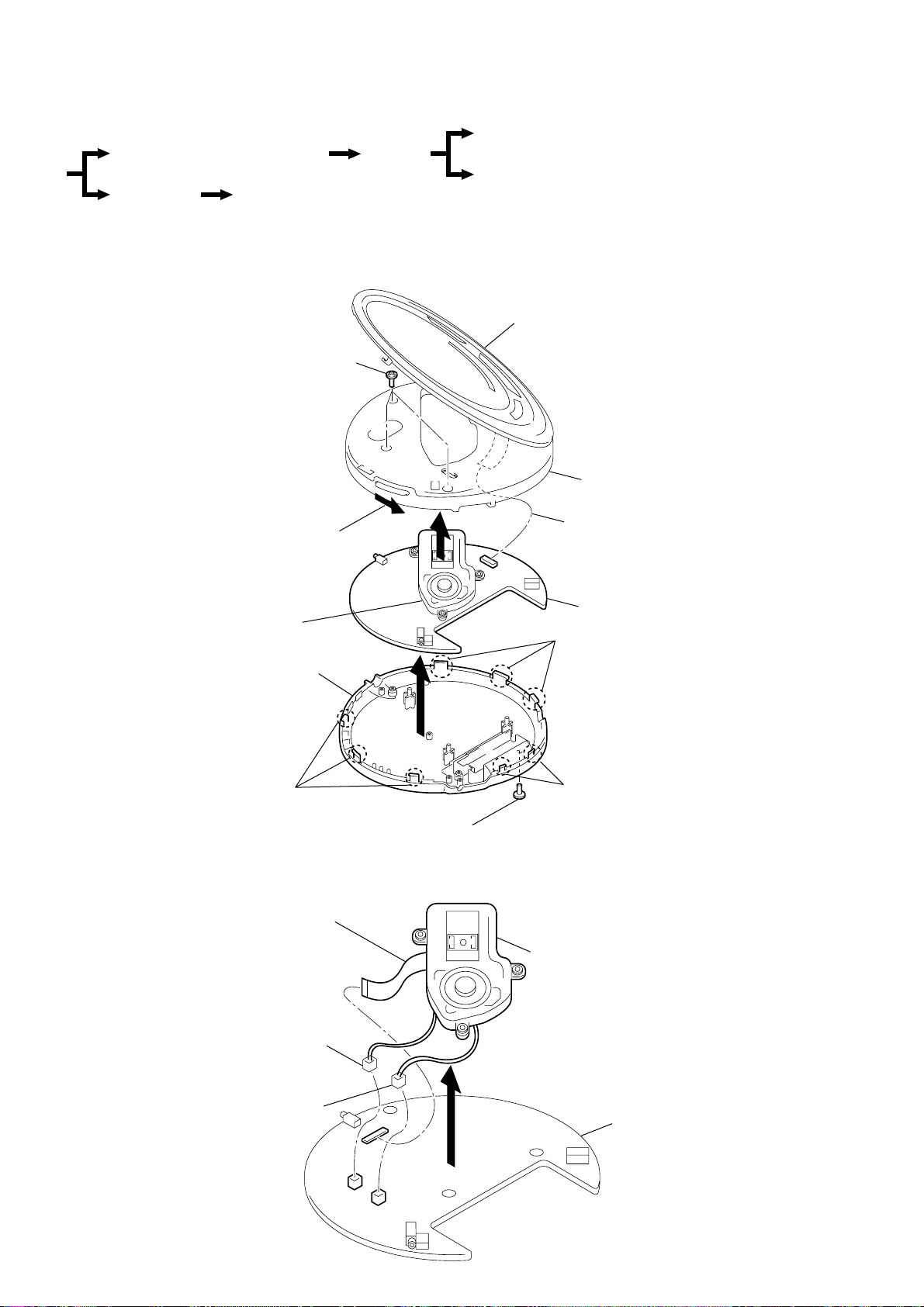
SECTION 3
DISASSEMBLY
z
The equipment can be removed using the following procedure.
“Motor ASSY, Turn table (Spindle) (M901)”
Cabinet (rear) sub ASSY, Main board MD ASSY
Set
Cabinet (front)
“Lid, Upper”, Switch unit
Note : Follow the disassembly procedure in the numerical order given.
3-1. CABINET (REAR) SUB ASSY, CABINET (FRONT), MAIN BOARD
3
Screws (B2 2x6)
“Motor ASSY (Sled) (M902)”, Optical pick-up (DAX-23E)
Lid ASSY (upper)
Cabinet (front)
3-2. MD ASSY
2
OPEN
MD ASSY
Cabinet (rear) sub ASSY
4
Claws
3
Optical pick-up
flexible board
7
1
Screws (B2 2x6)
5
6
4
Claws
4
MD ASSY
Flexible board (CN801)
Main board
Claws
2
CN503 (White)
1
CN502 (Green)
Main boar
6
D-E666/EJ620/EJ621/EJ622/EJ623/EJ625/EJ626CK
e
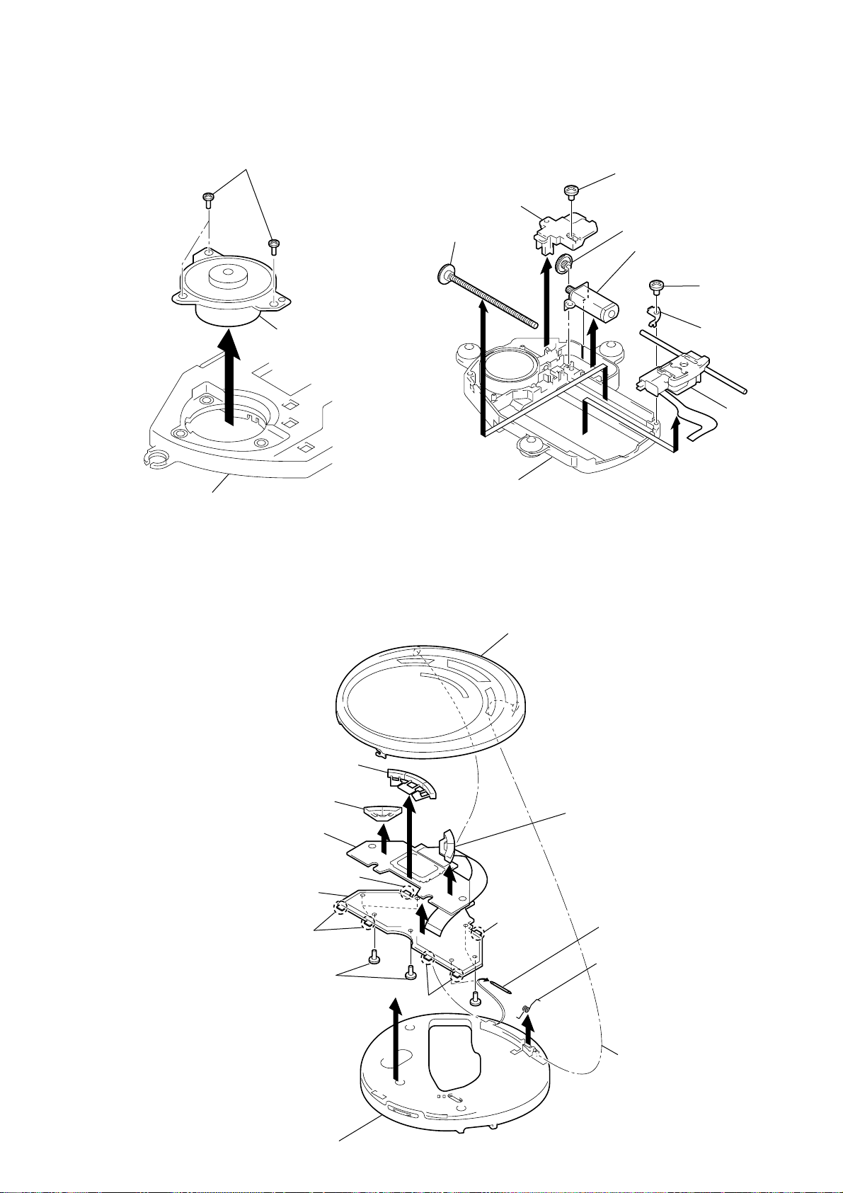
3-3. “MO TOR ASSY , TURN T ABLE
(SPINDLE) (M901)”
1 Screws
(B1.7x5)
Motor ASSY, Turn tabl
(Spindle) (M901)
2
Chassis
3-4. “MOTOR ASSY (SLED) (M902)”,
OPTICAL PICK-UP (DAX-23E)
1 Screw (B 1.7x5)
Cover, Gear
Screw ASSY, Feed
2
5
Chassis
Gear B
3
Motor ASSY (Sled) (M902)
4 Screw
(P 1.4x3.5)
Retainer, shaft
Optical pick-up
(DAX-23E)
6
3-5. “LID, UPPER”, SWITCH UNIT
0
Button (mode)
9
Button (FF and REW)
8
Switch unit
7
Cover, lid
6
Claws
5
Screws
6
Claw
4
6
Claws
Lid ASSY (upper)
!¡
6
Claw
Button (play)
1
Shaft lock
3
Spring (full open)
Cabinet (front)
2
7
D-E666/EJ620/EJ621/EJ622/EJ623/EJ625/EJ626CK
)
3
0
SECTION 4
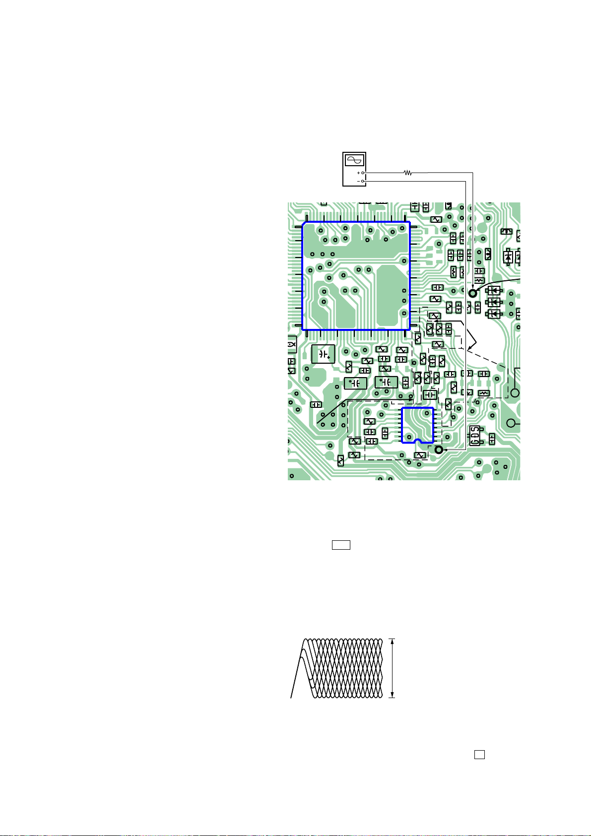
ELECTRICAL ADJUSTMENTS
The CD section adjustments are done automatically in this set.
Precautions for Check
1. Perform check in the order given.
2. Use YEDS-18 disc (Part No.: 3-702-101-01) unless otherwise
indicated.
3. Power supply voltage requirement : DC4.5 V in DC IN jack.
(J401)
VOLUME button : Minimum
AVLS switch : NORM
HOLD switch : OFF
Focus bias Check
Condition:
• Hold the set in horizontal state.
Connection:
oscilloscope
(AC range)
[ MAIN BOARD] (Side B)
C635
C632
P650
120
1
5
10
15
20
35
30
31
601
C621
2
TP441
C622
XCEPT
S MODEL
8
115
35
C610
TP410
TP426
R2
110
IC601
40
R601
R1
R408
105
45
R600
C625
R506
C505
C629
95
100
80
65
55
50
60
R632
R611
C627
C616
R612
C623
C626
13
16
C504
C506
US MODEL
2 K
91
85
75
70
61
C611
IC500
Ω
TP431 (GND)
R622
90
TP640
TP639
TP638
C609
R606
R603
R602
R504
C612
R500
R503
R650
C503
R502
TP431
TP629 (RF)
L6
C6
C628
C608
C605
R610
R605
R604
C602
R657
R614
C613
R616
R613
R617
89
R615
5
1
GND
L201
C601
C607
R609
C603
R607
EXCEPT
US MODEL
C614
Q405
TP416
TP818
C606
R608
D302
C604
L301
TP301
C615
R619
C407
L101
R412
D102
TP201
D202
D203
Procedure:
1. Connect the oscilloscope to the test points TP629 (RF) and TP431
(GND) on the MAIN board.
2. Set a disc. (YEDS-18)
3. Press the u button.
4. Check the oscilloscope waveform is as shown below.
A good eye pattern means that the diamond shape (◊) in the center of the waveform can be clearly distinguished.
RF Signal reference Waveform (Eye Pattern)
VOLT/DIV : 100 mV (With the 10 : 1 probe in use)
TIME/DIV : 500ns
RF level
0.4 to 0.65 Vp-p (Except US model
0.35 to 0.65 Vp-p (US model)
To watch the eye pattern, set the oscilloscope to AC range and
increase the vertical sensitivity of the oscilloscope for easy
watching.
5. Stop revolving of the disc motor by pressing the x button.
8
D-E666/EJ620/EJ621/EJ622/EJ623/EJ625/EJ626CK
SECTION 5
DIAGRAMS
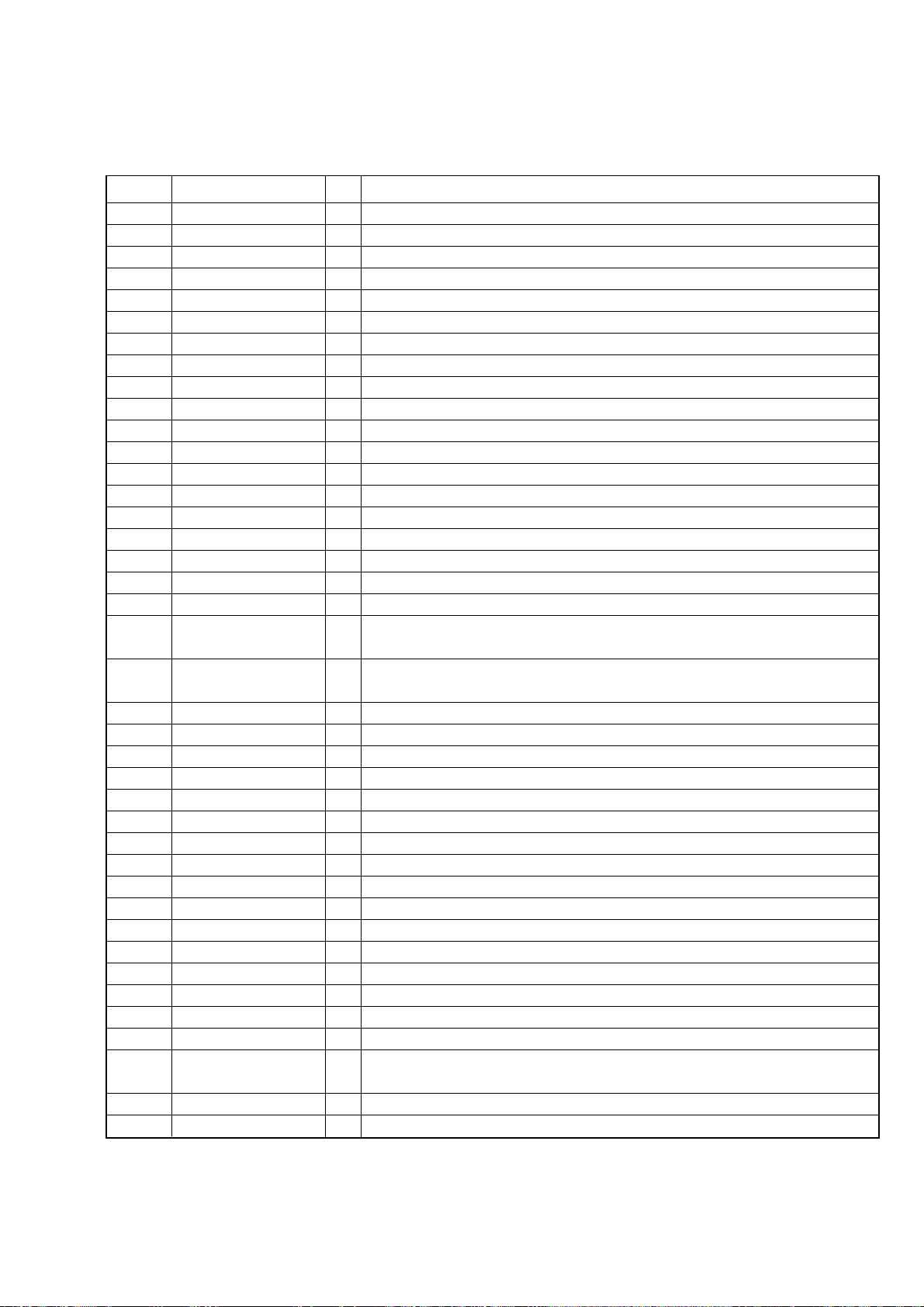
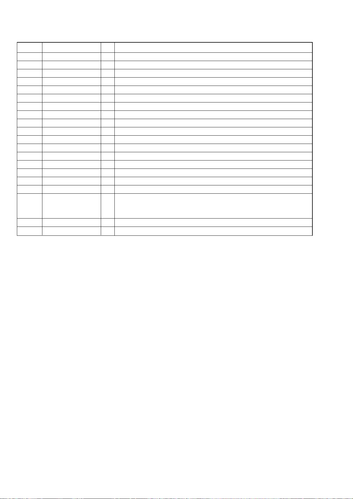
5-1. EXPLANATION OF IC TERMINALS
IC801 (SYSTEM CONTROLLER) T5U87-05 (E666/EJ625: E13, HK, KR, CH, AUS),
TMP88CM22F-MIRX-1 (EJ620/EJ621/EJ622/EJ623/EJ625: US, CND, AEP, UK, G, FR, EE/EJ626CK)
Pin No. Pin name I/O Description
1 VSS — Ground terminal.
2 IRRMCO — Not used (OPEN).
3 FOKI I Focus OK signal input from the digital servo processor (IC601). “L”: NG, “H”: OK
4 AGCPWM O AGC control pulse signal output terminal.
5 RESERVE — Not used (OPEN).
6 RESERVE — Not used (OPEN).
7 AMUTE O Analog audio muting ON/OFF control signal output terminal. “H”: muting ON
8 VCC2 ON O VCC2 voltage control signal output terminal.
9 XRST O Reset signal output to IC601. “L”: reset
10 SCK O Serial data transfer clock signal output to IC601.
11 MSDTI I Serial data input from the IC601.
12 MSDTO O Serial data output to IC601.
13 WAKE UP O WAKE-UP control signal output terminal (for system standby reset).
14 SEL I Plug-in detection signal input terminal of LINE OUT/OPTICAL OUT.
15 CHGMNT I Battery charge voltage detection input from the power control (IC401).
16 KEY2 I Volume key input terminal.
17 BATMNT I Battery voltage detection signal input terminal
18 KEY1 I Key input terminal.
19 RMKEY I Key input from the headphone with remote commander (A/D input).
20 DCINMNT I
21 OPEN I
22 VREFL I Reference voltage input terminal (0V) for A/D converter.
23 VREFH I Reference voltage input terminal (+2V) for A/D converter.
24 VDD — Power supply terminal (+2V).
25 SCOR I Sub-code sync (S0+S1) detection signal input from the IC601.
26 GRSCOR I GRSCOR signal input from the IC601.
27 MIR I FG pulse signal input.
28 BEEP O Beep sound output to the headphone amplifier (IC302).
29 RESERVE — Not used ( Fixed at “H”).
30 RESERVE — Not used ( Fixed at “H”).
31 RESERVE I Not used ( Fixed at “H”).
32 TSB O Communication data bus output of headphone with remote commander.
33 TXTSKIP — Not used (OPEN).
34 XDIG VOL — Not used (OPEN).
35 CD RW — Not used (OPEN).
36 COMPRESSION I G PROTECTION switch input.
37 DIG TU — Not used (Fixed at “H”).
38 AVLS I
39 HOLD I HOLD switch (S803) input terminal. “L”: hold ON, “H”: hold OFF
40 EXBAT I External battery detection signal input terminal.
DC input voltage detection input terminal (A/D input) and DC input jack use/no use
detection input terminal.
CD door open/close detection switch (S801) input terminal.
The stop status is reset with the falling edge of input signal.
AVLS (Automatic Volume Limiter System) switch (S803) input terminal.
“L”: normal mode, “H”: limit mode
9
D-E666/EJ620/EJ621/EJ622/EJ623/EJ625/EJ626CK
Pin No. Pin name I/O Description
41 BATDET I Battery detection input.
42 XHGOM O Optical pick-up power ON/OFF control signal output terminal. “L”: ON
43 XLAT O Serial data latch pulse signal output to IC601.
44 XSOE O Serial data output enable signal output terminal.
45 RESERVE — Not used ( Fixed at “H”).
46 XPOWLT O Latch signal output to the power control (IC401).
47 RESERVE — Not used (Fixed at “H”).
48 XAPC OFF O APC mute signal output terminal. “L”: mute
49 SEG15 — Not used (open).
50 to 64 SEG14 to SEG0 O Segment drive signal output to the liquid crystal display.
65 to 68 COM3 to COM0 O Common drive signal output to the liquid crystal display.
69 to 71 V3 to V1 O Bias signal output to the liquid crystal display driver.
72, 73 C1, C0 O Capacitor connected terminal for the liquid crystal display driver voltage-up.
74 STOP O VCD control stop signal output terminal. Not used (Fixed at “L”).
75 TEST I Test terminal for IC (Fixed at “L”).
76 XVCC2SD O VCC2 voltage control signal output terminal.
77 XLED O LCD back light control signal output to the liquid crystal display. (EJ616CK)
System reset signal input from the power control (IC401). “L”: reset
78 RESET I For several hundreds msec. after the power supply rises, “L” is input, then it changes to
“H”
79 XIN I System clock input terminal.
80 XOUT — Not used (OPEN).
10
 Loading...