

Page 1
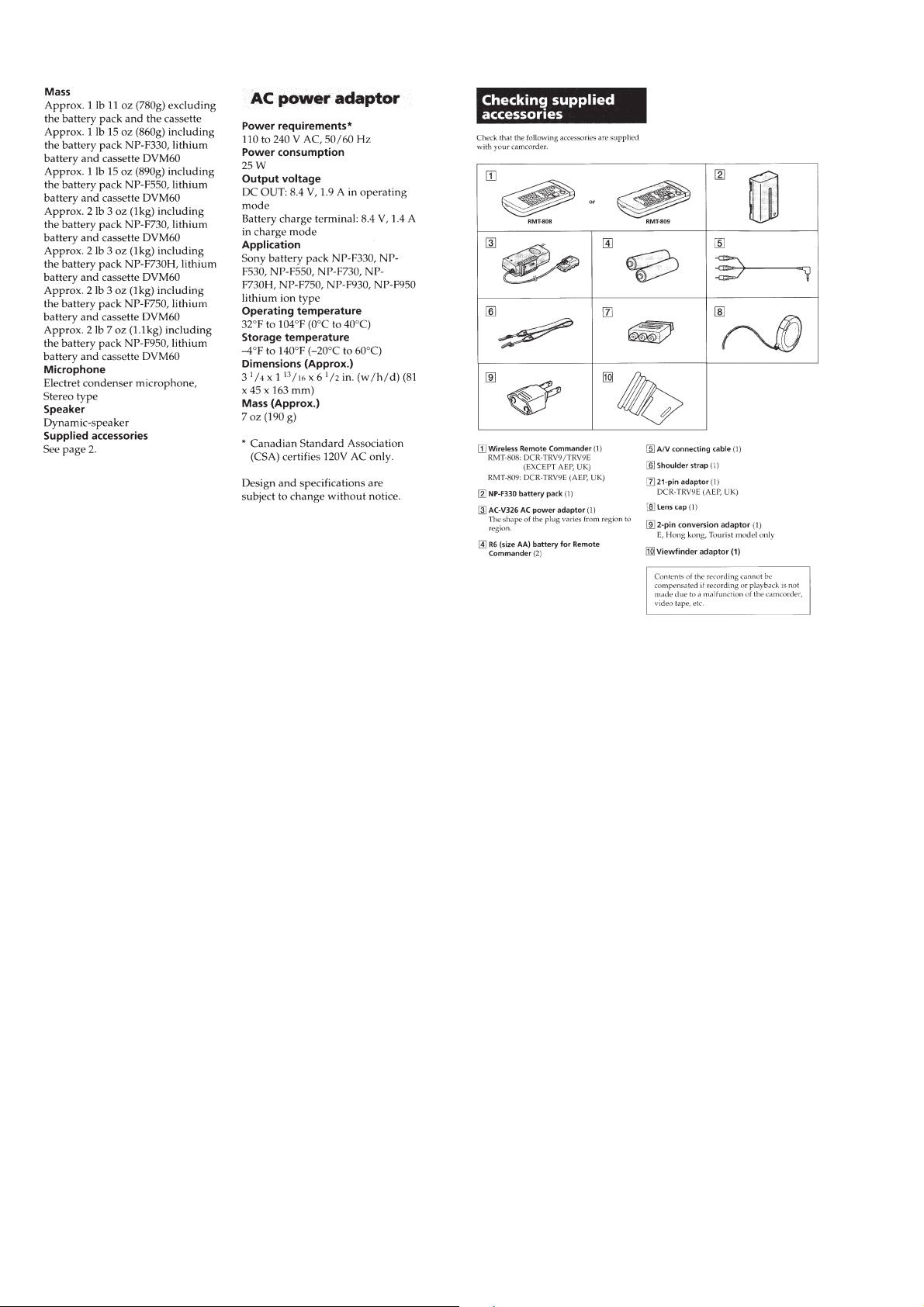
DCR-TRV9/TRV9E
RMT-808/809
SERVICE MANUAL
Ver 1.2 2001.01
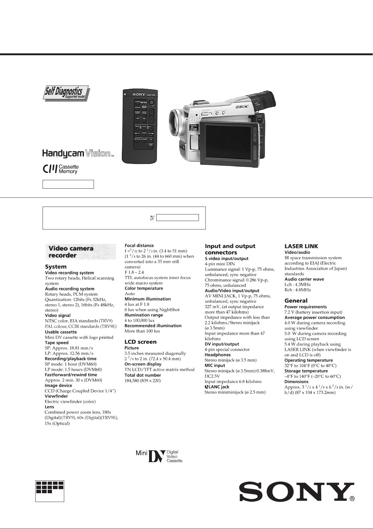
Photo: DCR-TRV9E
RMT-809
C MECHANISM
For MECHANISM ADJUSTMENTS, refer to the “DV
MECHANICAL ADJUSTMENT MANUAL
(9-974-050-11)
C MECHANISM ”
SPECIFICATIONS
US Model
Canadian Model
DCR-TRV9
AEP Model
UK Model
Australian Model
Chinese Model
DCR-TRV9E
E Model
Hong Kong Model
Tourist Model
DCR-TRV9/TRV9E
NTSC model: DCR-TRV9
PAL model: DCR-TRV9E
MICROFILM
— Continued on next page —
DIGITAL VIDEO CAMERA RECORDER
Page 2
SAFETY-RELATED COMPONENT WARNING!!
COMPONENTS IDENTIFIED BY MARK ! OR DO TTED LINE WITH
MARK ! ON THE SCHEMATIC DIAGRAMS AND IN THE PARTS
LIST ARE CRITICAL TO SAFE OPERATION. REPLACE THESE
COMPONENTS WITH SONY PARTS WHOSE PART NUMBERS
APPEAR AS SHOWN IN THIS MANUAL OR IN SUPPLEMENTS
PUBLISHED BY SONY.
SAFETY CHECK-OUT
After correcting the original service problem, perform the following
safety checks before releasing the set to the customer.
ATTENTION AU COMPOSANT AYANT RAPPORT
À LA SÉCURITÉ!
LES COMPOSANTS IDENTIFÉS P AR UNE MARQUE ! SUR LES
DIAGRAMMES SCHÉMA TIQUES ET LA LISTE DES PIÈCES SONT
CRITIQUES POUR LA SÉCURITÉ DE FONCTIONNEMENT. NE
REMPLACER CES COMPOSANTS QUE PAR DES PIÈSES SONY
DONT LES NUMÉROS SONT DONNÉS DANS CE MANUEL OU
DANS LES SUPPÉMENTS PUBLIÉS PAR SONY.
1. Check the area of your repair for unsoldered or poorly-soldered
connections. Check the entire board surface for solder splashes
and bridges.
2. Check the interboard wiring to ensure that no wires are
"pinched" or contact high-wattage resistors.
3. Look for unauthorized replacement parts, particularly
transistors, that were installed during a previous repair . Point
them out to the customer and recommend their replacement.
— 2 —
4. Look for parts which, through functioning, show obvious signs
of deterioration. Point them out to the customer and
recommend their replacement.
5. Check the B+ voltage to see it is at the values specified.
6. Flexible Circuit Board Repairing
• Keep the temperature of the soldering iron around 270˚C
during repairing.
• Do not touch the soldering iron on the same conductor of the
circuit board (within 3 times).
• Be careful not to apply force on the conductor when soldering
or unsoldering.
Page 3

TABLE OF CONTENTS
SERVICE NOTE
1. POWER SUPPLY DURING REPAIRS.............................6
2. HOW TO TAKE A CASSETTE OUT WHEN THE MAIN
POWER CANNOT BE TURNED ON...............................6
SELF-DIAGNOSIS FUNCTION
1. SELF-DIAGNOSIS FUNCTION.......................................7
2. SELF-DIAGNOSIS DISPLAY..........................................7
3. SERVICE MODE DISPLAY.............................................7
3-1.Display Method..................................................................7
3-2.Switching of Backup No....................................................7
3-3.End of Display....................................................................7
4. SELF-DIAGNOSIS CODE TABLE...................................8
1. GENERAL
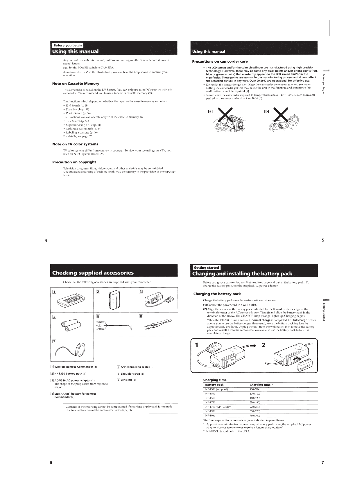
Before you begin
Using this manual..................................................................1-1
Checking supplied accessories..............................................1-1
Getting started
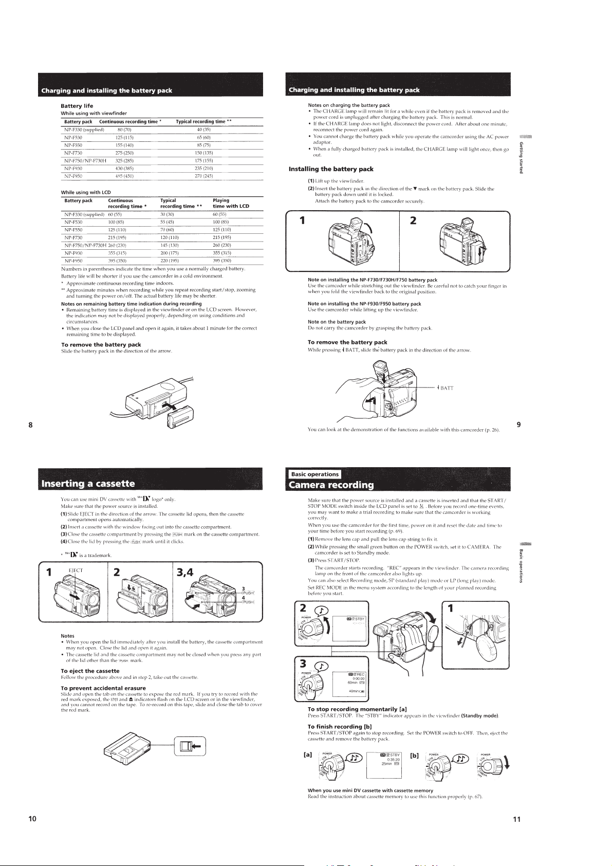
Charging and installing the battery pack...............................1-1
Inserting a cassette.................................................................1-2
Basic operations
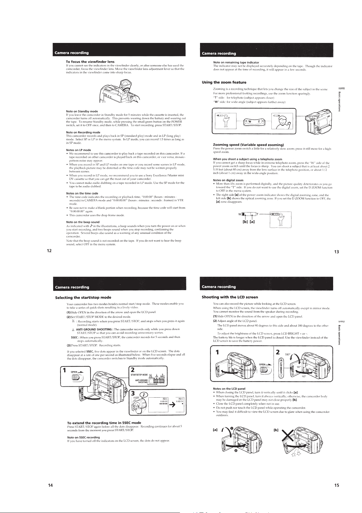
Camera recording...................................................................1-2
Hints for better shooting........................................................1-4
Checking the recorded picture...............................................1-4
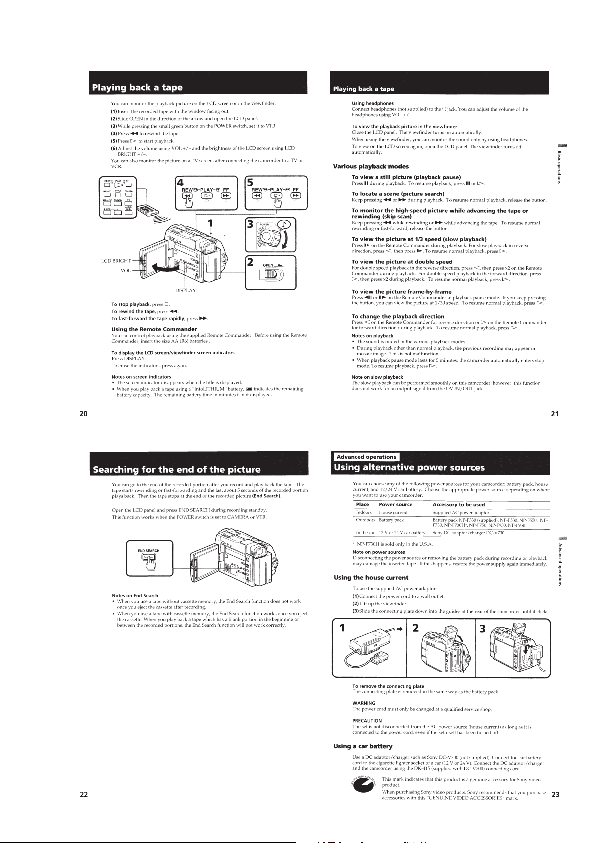
Playing back a tape................................................................1-5
Searching for the end of the picture.......................................1-5
Advanced operations
Using alternative power sources............................................1-5
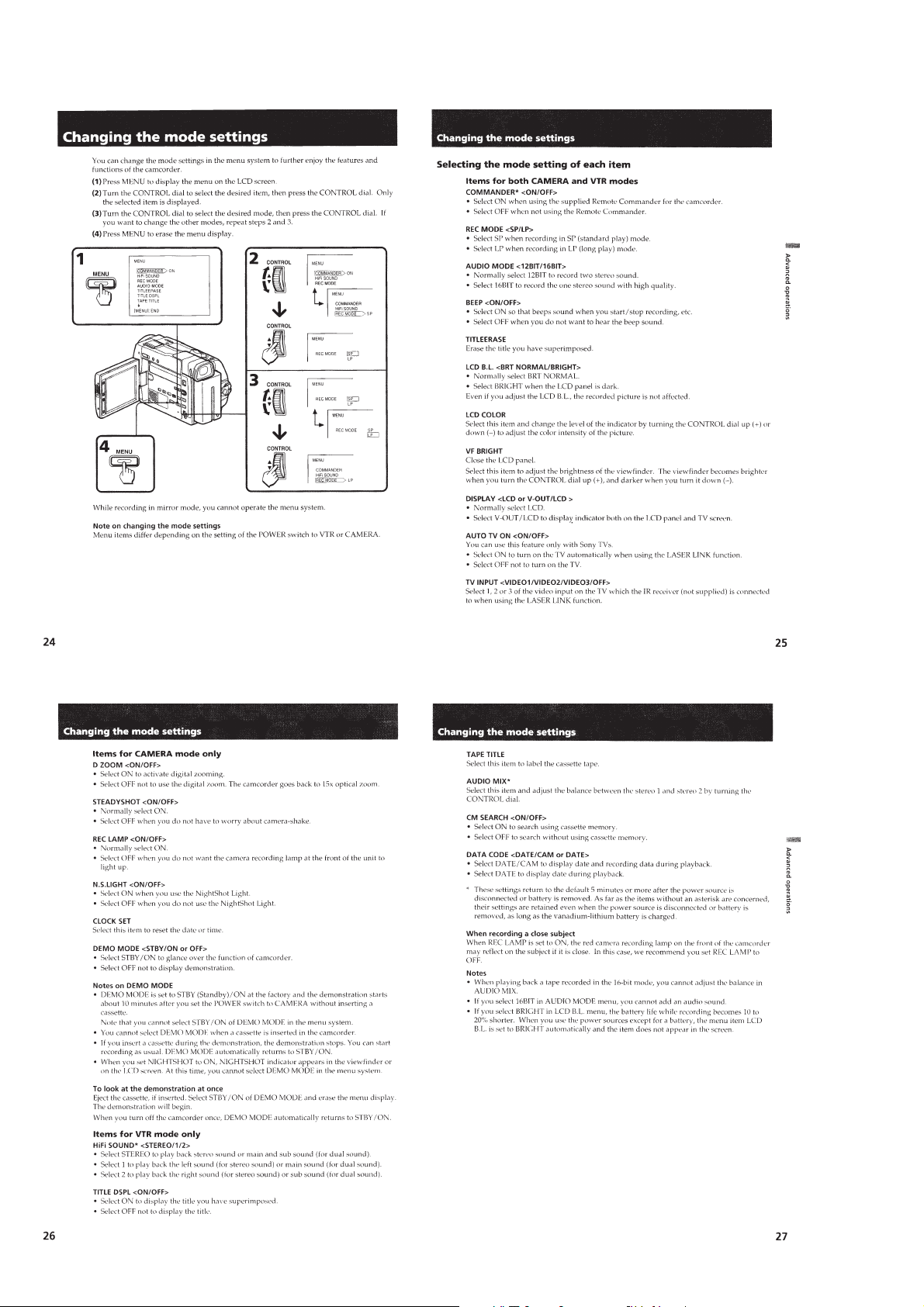
Changing the mode settings...................................................1-6
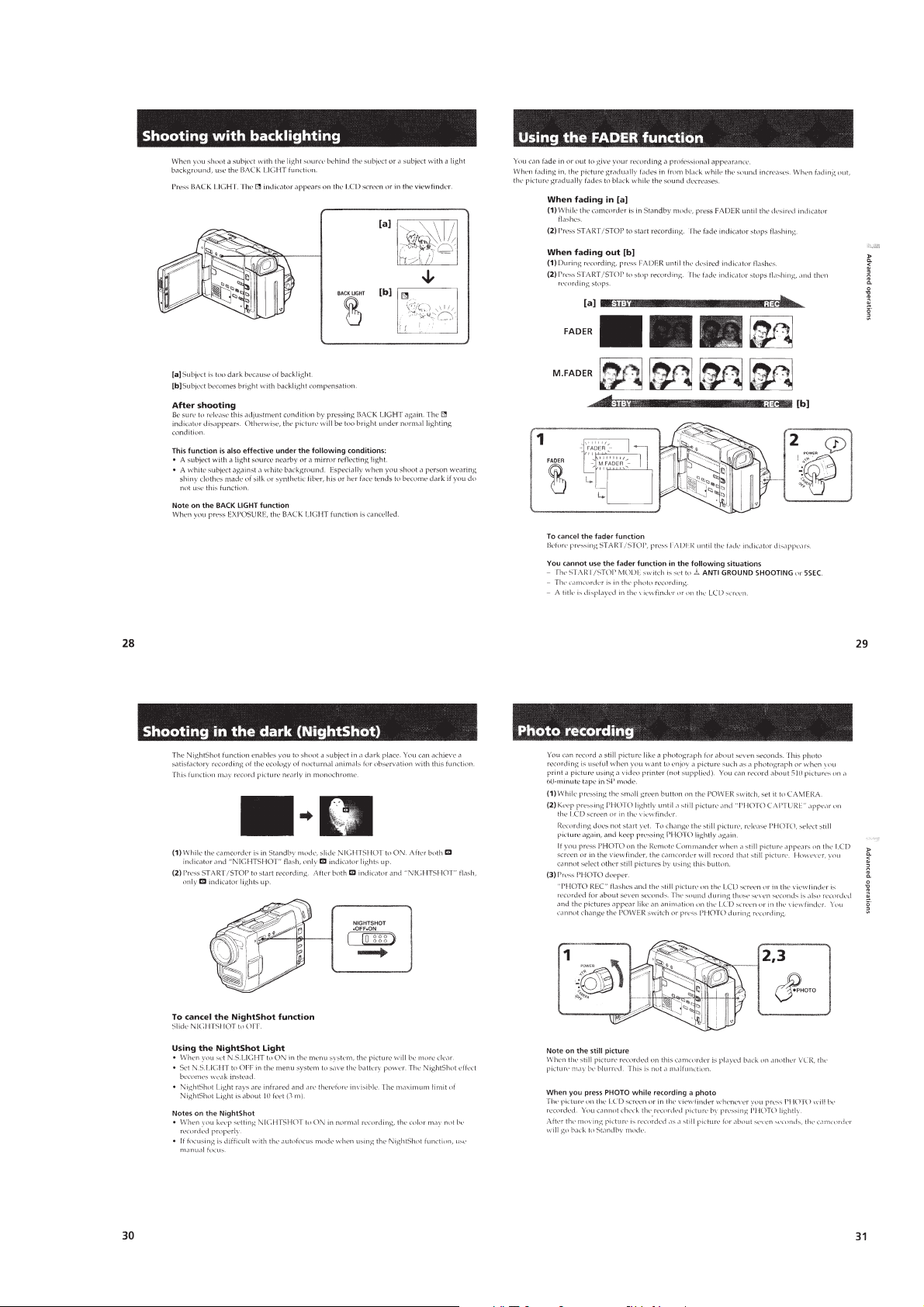
Shooting with backlighting....................................................1-7
Using the FADER function....................................................1-7
Shooting in the dark (Nightshot)...........................................1-7
Photo recording......................................................................1-7
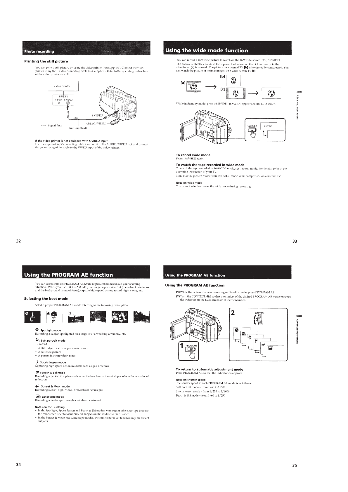
Using the wide mode function...............................................1-8
Using the PROGRAM AE function.......................................1-8
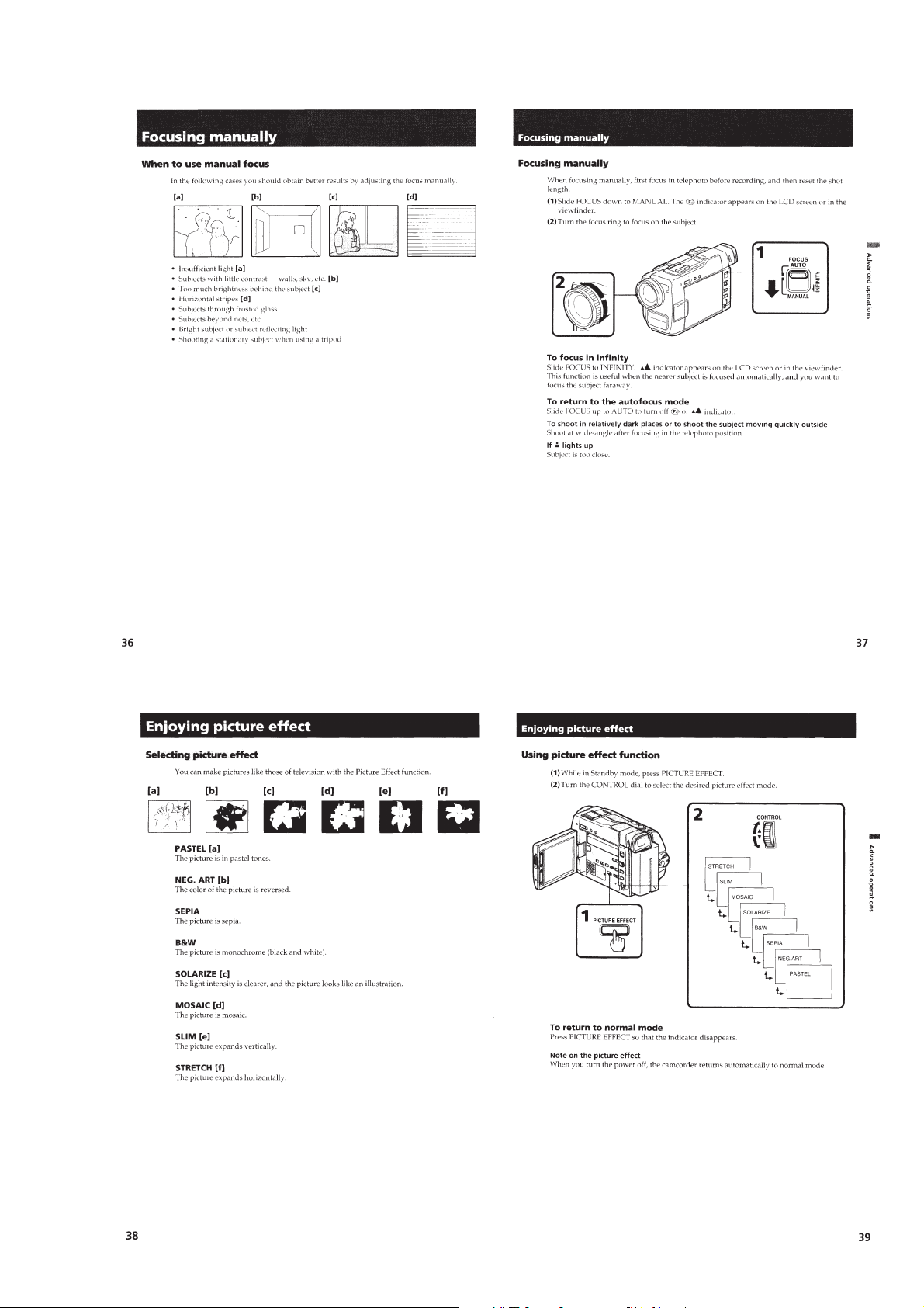
Focusing manually.................................................................1-9
Enjoying picture effect...........................................................1-9
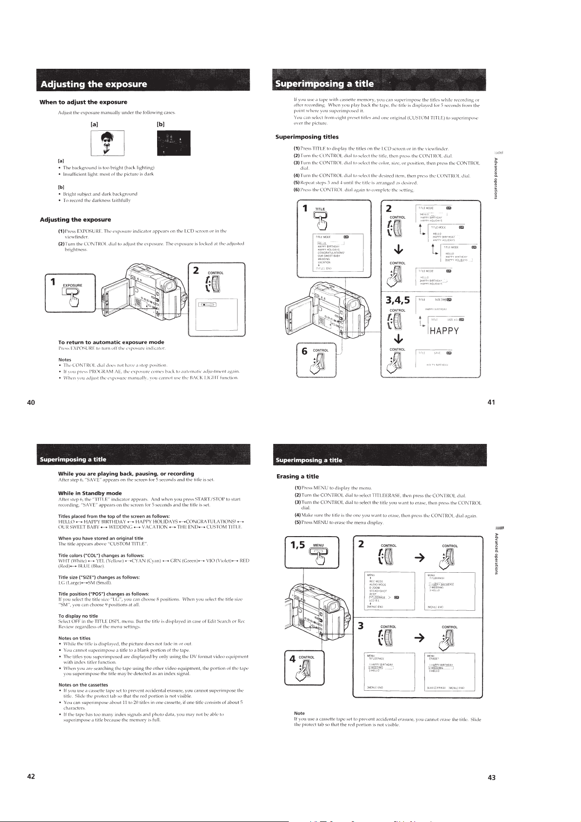
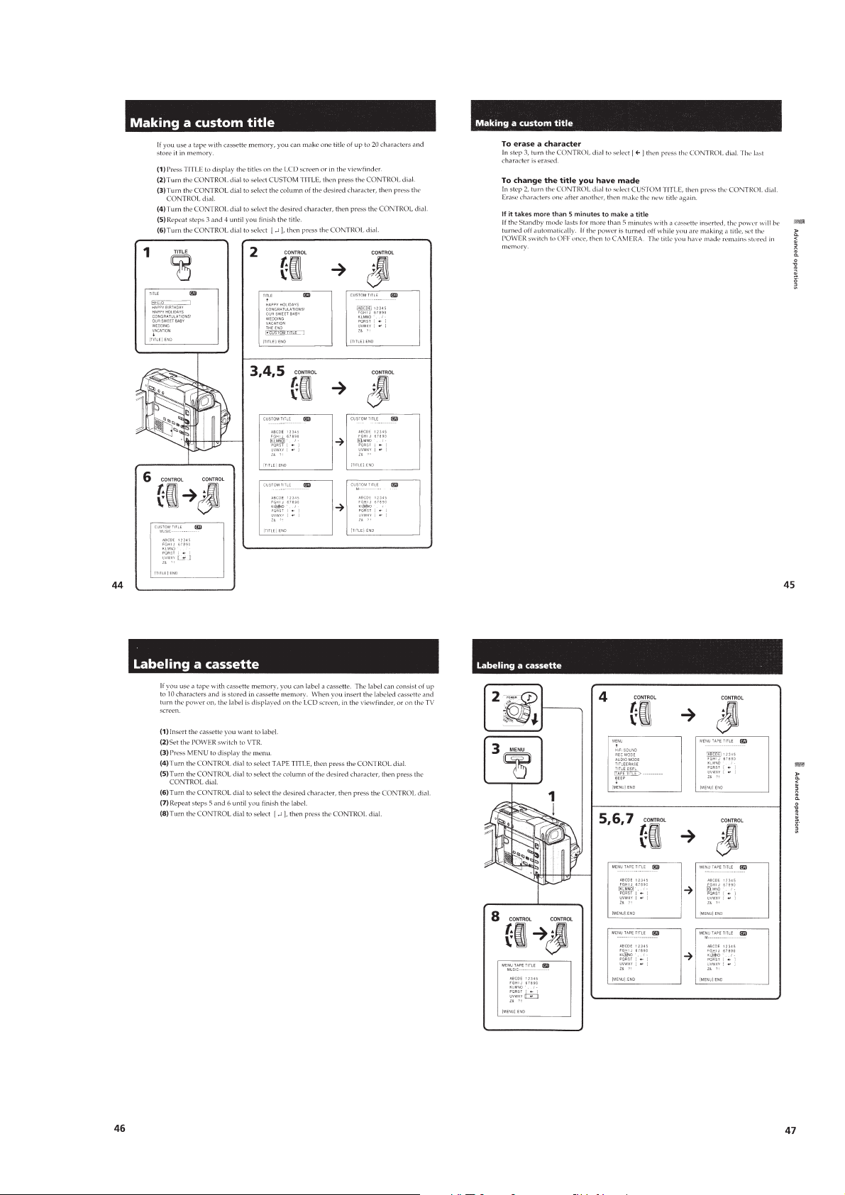
Adjusting the exposure........................................................1-10
Superimposing a title...........................................................1-10
Making a custom title..........................................................1-11
Labeling a cassette...............................................................1-11
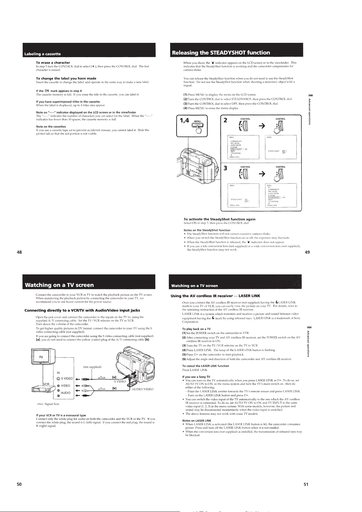
Releasing the STEADYSHOT function..............................1-12
Watching on a TV screen.....................................................1-12
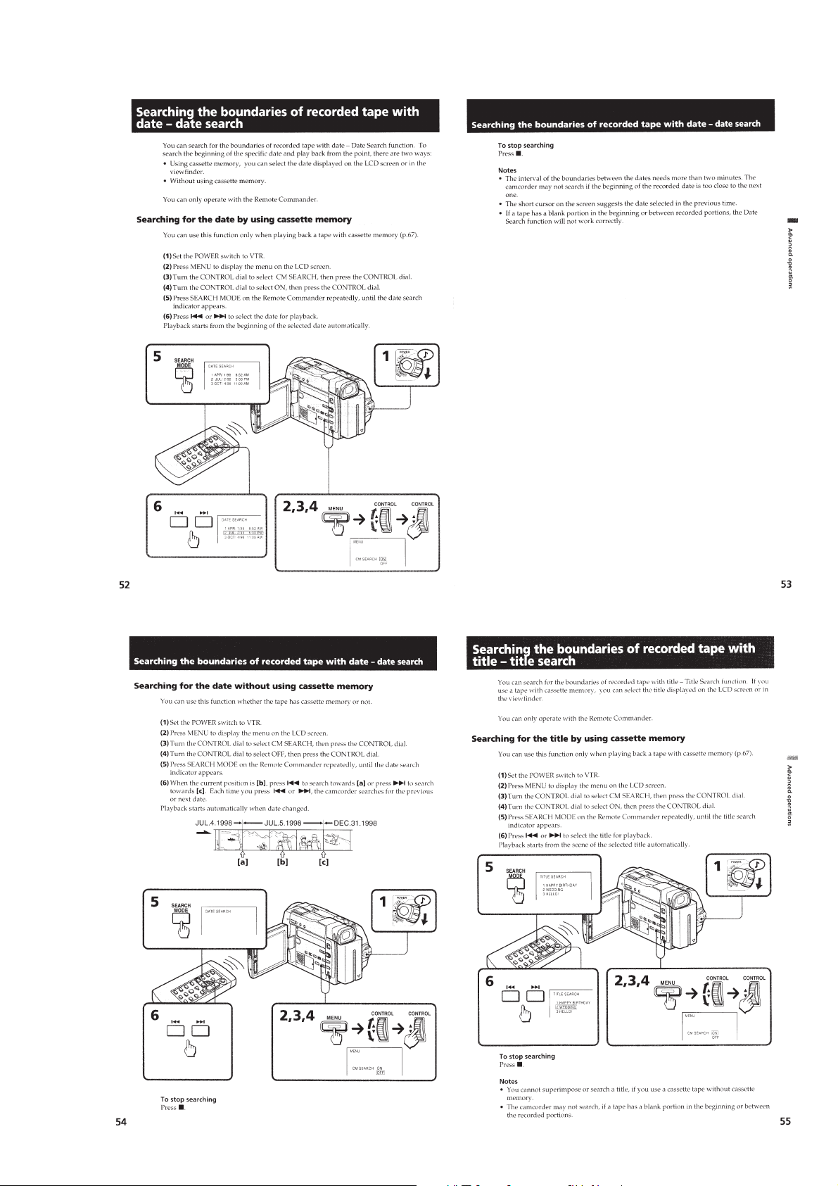
Searching the boundaries of recorded tape with
date - date search.................................................................1-13
Searching the boundaries of recorded tape with
title - title search..................................................................1-13
Searching for a photo - photo search/photo scan.................1-14
Returning to a pre-registered position.................................1-14
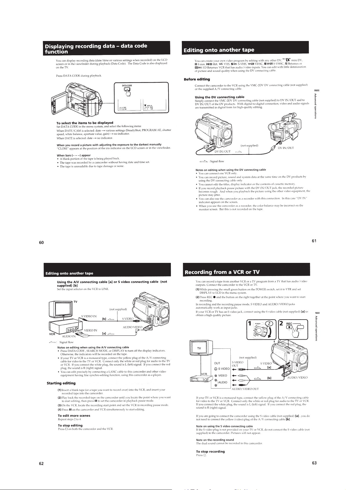
Displaying recording data - data code function...................1-15
Editing onto another tape.....................................................1-15
Recording from a VCR or TV.............................................1-15
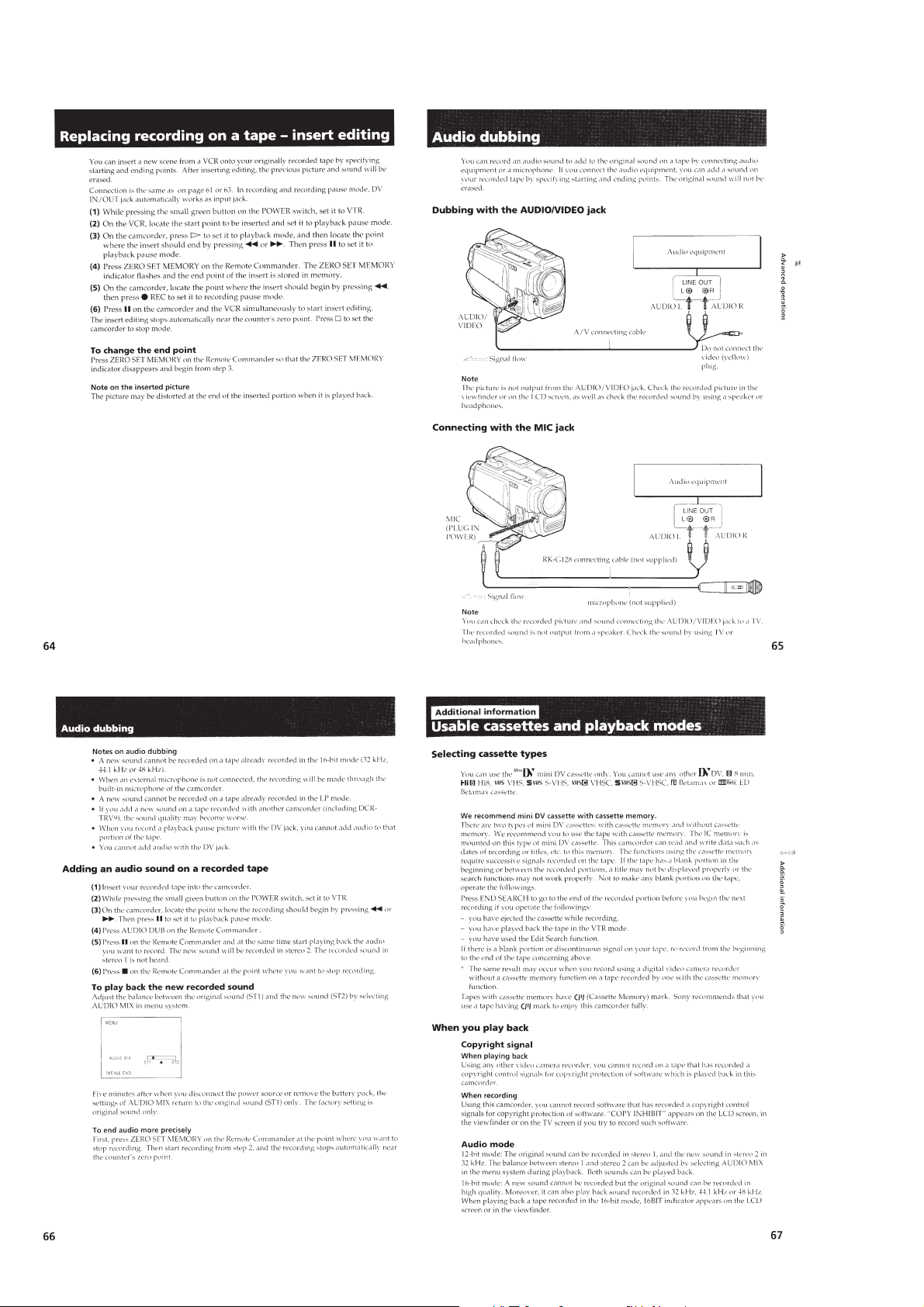
Replacing recording on a tape - insert editing.....................1-16
Audio dubbing.....................................................................1-16
Additional information
Usable cassette and playback modes...................................1-17
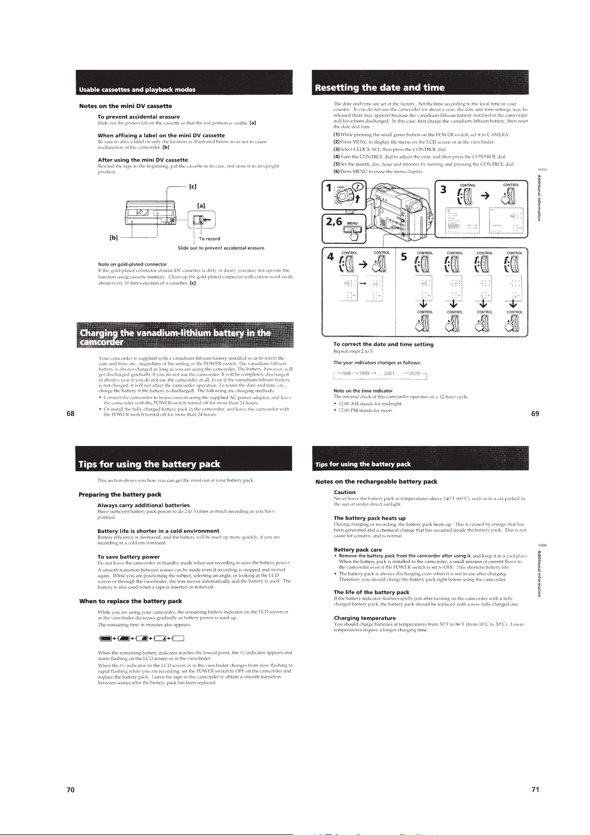
Resetting the date and time..................................................1-17
Charging the vanadium-lithium battery in the camcorder...1-17
Tips for using the battery pack............................................1-17
Maintenance information and precautions...........................1-18
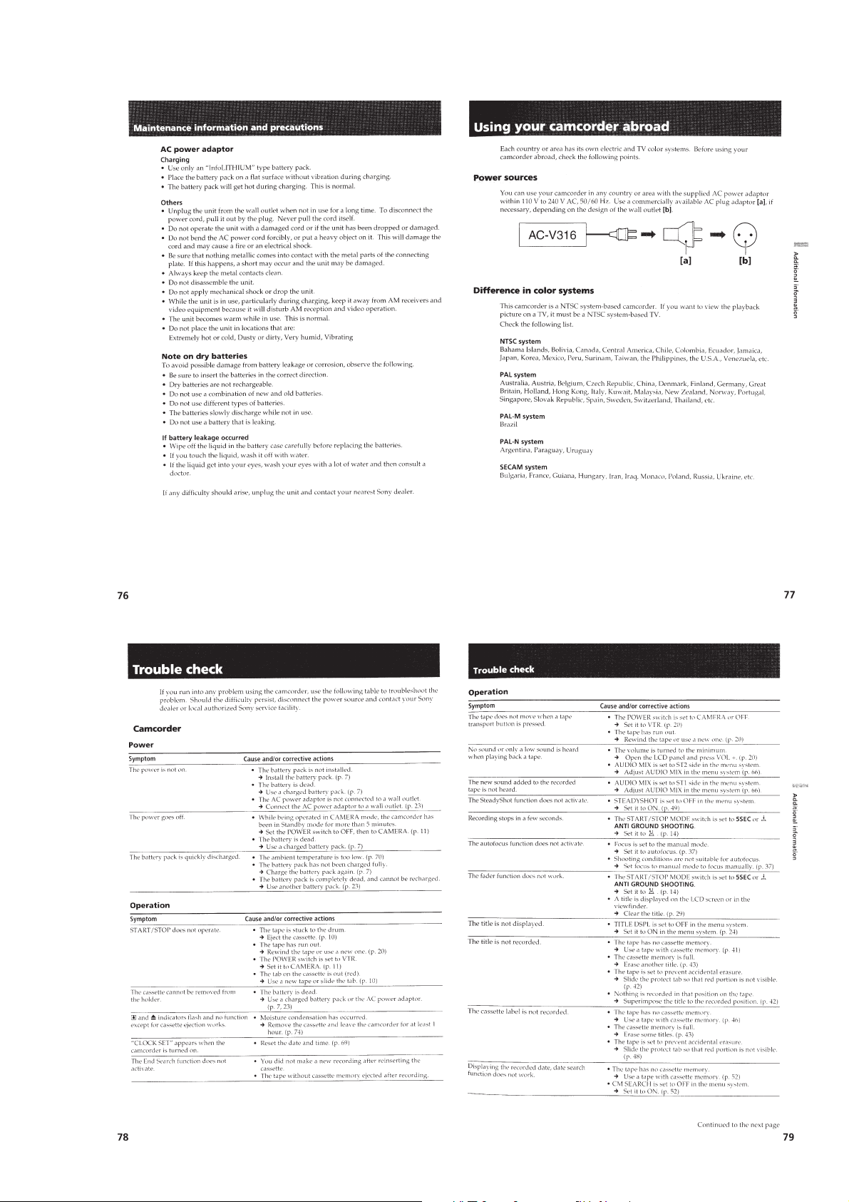
Using your camcorder abroad..............................................1-19
Trouble check......................................................................1-19
Self-diagnosis function........................................................1-20
Identifying the parts.............................................................1-21
Warning indicators...............................................................1-23
2. DISASSEMBLY
2-1.F PANEL ASSEMBLY...................................................2-1
2-2.CABINET (L), CABINET (R) ASSEMBLIES...............2-1
2-3.CABINET (R) ASSEMBLY............................................2-2
2-4.EVF ASSEMBLY............................................................2-2
2-5.EVF CABINET (UPPER) ASSEMBLY, EVF CABINET
(LOWER) ASSEMBLIES...............................................2-3
2-6.LCD ASSEMBLY...........................................................2-3
2-7.AU-202 BOARD, DD-106 BOARD, BATTERY HOLDER
ASSEMBLY....................................................................2-4
2-8.ZOOM LENS..................................................................2-4
2-9.VC-206 BOARD.............................................................2-4
2-10.MECHANISM DECK.....................................................2-5
2-11.CABINET (L) ASSEMBLY............................................2-5
2-12.FP-647, FP-648 FLEXIBLE BOARD,
VI-148 BOARD...............................................................2-6
2-13.SERVICE POSITION.....................................................2-6
2-14.CIRCUIT BOARD LOCATION.....................................2-7
3. BLOCK DIAGRAMS
3-1.OVERALL BLOCK DIAGRAM (1)..............................3-1
3-2.OVERALL BLOCK DIAGRAM (2)..............................3-4
3-3.POWER BLOCK DIAGRAM.........................................3-7
4. PRINTED WIRING BOARDS AND
SCHEMATIC DIAGRAMS
4-1.FRAME SCHEMATIC DIAGRAM................................4-1
4-2.PRINTED WIRING BOARDS AND
SCHEMATIC DIAGRAMS............................................4-4
•CD-185 (CCD IMAGER)
PRINTED WIRING BOARD.........................4-5
•CD-185 (CCD IMAGER)
SCHEMATIC DIAGRAM..............................4-9
•VC-206 (CAMERA, VIDEO IN/OUT, BLOCKING,
ECC, TBC, CHCO, AUDIO PROCESS, RF INTERFACE, REC/PB HEAD AMP, DV PROCESS, SERVO,
HI CONTROL)
PRINTED WIRING BOARD.......................4-14
•VC-206 (CAMERA) SCHEMATIC DIAGRAM.......4-19
•FP-647 (DV, LINE JACKS)
PRINTED WIRING BOARD.......................4-23
•VC-206 (VIDEO IN/OUT), FP-647 (DV, LINE JACKS)
SCHEMATIC DIAGRAM............................4-24
•VC-206 (VIDEO DECODER)
SCHEMATIC DIAGRAM............................4-27
•VC-206 (BLOCKING, COMPRESS)
SCHEMATIC DIAGRAM...........................4-32
•VC-206 (ECC, TBC, CHCO)
SCHEMATIC DIAGRAM............................4-35
•VC-206 (AUDIO PROCESS)
SCHEMATIC DIAGRAM............................4-38
•VC-206 (RF INTERFACE 1),
FP-676 (LANC, PHONES JACKS)
SCHEMATIC DIAGRAM............................4-41
•FP-676 (LANC, PHONES JACKS)
PRINTED WIRING BOARD.......................4-43
•VC-206 (SIGNAL PROCESS CONTROL),
FP-647 (LANC, PHONES JACKS)
SCHEMATIC DIAGRAMS..........................4-44
•VC-206 (RF INTERFACE 2)
SCHEMATIC DIAGRAM............................4-47
•VC-206 (REC/PB HEAD AMP)
SCHEMATIC DIAGRAM............................4-51
•VC-206 (DV PROCESS)
SCHEMATIC DIAGRAM............................4-55
— 3 —
Page 4

• VC-206 (SER VO),
FP-594 (LOADING MOTOR, SENSORS, SWITCHES)
SCHEMATIC DIAGRAMS..........................4-59
• FP-594 (LOADING MOTOR, SENSORS, SWITCHES)
PRINTED WIRING BOARD .......................4-62
• VC-206 (HI CONTROL), LI-64 (LITHIUM BATTERY)
SCHEMATIC DIAGRAM AND
PRINTED WIRING BOARD .......................4-63
• MA-322 (MIC AMP, A/V RF CONVERTER,
IR RECEIVER, SIRCS DET)
PRINTED WIRING BOARD .......................4-66
• MA-322 (SIRCS DET) SCHEMATIC DIAGRAM....4-68
• MA-322 (MIC AMP, SELECT)
SCHEMATIC DIAGRAM ............................4-69
• MA-322 (A/V RF CONVERTER, IR RECEIVER,
SIRCS DET)
SCHEMATIC DIAGRAM ............................4-71
• AU-202 (SP/HP AMP, AUDIO DSP, MIC AMP)
PRINTED WIRING BOARD .......................4-74
• AU-202 (SP/HP AMP) SCHEMATIC DIAGRAM ....4-79
• AU-202 (AUDIO DSP, MIC AMP)
SCHEMATIC DIAGRAM ............................4-82
• VI-148 (VIDEO INTERFACE)
SCHEMATIC DIAGRAM ............................4-85
• VI-148 (Y/C SEP., A/D, DECODER, AFC)
SCHEMATIC DIAGRAM ............................4-87
• VI-148 (VIDEO INTERFACE, Y/C SEP., A/D, DECODER, AFC)
PRINTED WIRING BOARD .......................4-89
• KY-39 (PANEL FUNCTION SWITCH),
FP-649 (PANEL CONDITION DET.),
FP-657 (CONTROL SWITCHES)
SCHEMATIC DIAGRAM ............................4-92
• KY-39 (PANEL FUNCTION SWITCH),
FP-649 (PANEL CONDITION DET.),
FP-657 (CONTROL SWITCHES)
PRINTED WIRING BOARDS .....................4-95
• PD-98 (RGB DECODER, TIMING GENERATOR,
BACK LIGHT)
PRINTED WIRING BOARD .......................4-99
• PD-98 (RGB DECODER)
SCHEMATIC DIAGRAM ..........................4-103
• PD-98 (TIMING GENERATOR, BACK LIGHT)
SCHEMATIC DIAGRAM ..........................4-107
• LB-55 (EVF BACK LIGHT)
PRINTED WIRING BOARD AND
SCHEMATIC DIAGRAMS........................4-111
• VF-121 (COLOR EVF)
SCHEMATIC DIAGRAMS........................4-116
• VF-121 (COLOR EVF)
PRINTED WIRING BOARD .....................4-121
• DD-106 (POWER SUPPLY)
PRINTED WIRING BOARD .....................4-125
• DD-106 (POWER SUPPLY)
SCHEMATIC DIAGRAM ..........................4-129
5. ADJUSTMENTS
5-1. CAMERA SECTION ADJUSTMENT...........................5-1
1-1. PREPARATIONS BEFORE ADJUSTMENT
(CAMERA SECTION) ...................................................5-1
1-1-1.List of Service Tools ........................................................5-1
1-1-2.Preparations .....................................................................5-2
1-1-3.Precaution ........................................................................5-4
1. Setting the Switch............................................................ 5-4
2. Order of Adjustments ......................................................5-4
3. Subjects ........................................................................... 5-4
1-2. INITIALIZATION OF F, E PAGE DATA ....................... 5-5
1. Initializing the F, E Page Data ......................................... 5-5
2. Modification of F, E PAGE Data ..................................... 5-5
3. F Page Table ....................................................................5-5
4. E Page table ..................................................................... 5-8
1-3. CAMERA SYSTEM ADJUSTMENTS.......................... 5-9
1. 36 MHz Origin Oscillation Adjustment
(VC-206 board) ...............................................................5-9
2. Zoom Key Center Adjustment (VC-206 board) ..............5-9
3. HALL Adjustment .........................................................5-10
4. Flange Back Adjustment ...............................................5-11
4-1. Flange Back Adjustment (1)..........................................5-11
4-2. Flange Back Adjustment (2)..........................................5-11
5. Flange Back Check........................................................5-12
6. Picture Frame Setting ....................................................5-12
7. G-CAM flip Adjustment................................................5-13
8. Color Reproduction Adjustment....................................5-14
9. MAX GAIN Adjustment ...............................................5-15
10. Auto White Balance Standard Data Input .....................5-15
11. Auto White Balance Adjustment ...................................5-16
12. White Balance Check ....................................................5-16
13. Angular Velocity Sensor Sensitivity Adjustment ..........5-17
1-4. COLOR ELECTRONIC VIEWFINDER SYSTEM
ADJUSTMENT.............................................................5-18
1. EVF Initial Data Input ...................................................5-18
2. VCO Adjustment (VF-121 board).................................5-19
3. Bright Adjustment (VF-121 board) ...............................5-19
4. Contrast Adjustment (VF-121 board)............................5-20
5. Backlight Consumption Current Adjustment
(VF-121 board)..............................................................5-20
6. White Balance Adjustment (VF-121 board)..................5-21
1-5. LCD SYSTEM ADJUSTMENT ...................................5-22
1. LCD Initial Data Input ..................................................5-22
2. VCO Adjustment (PD-98 board)................................... 5-23
3. Horizontal Position check (PD-98 board) .....................5-23
4. D range Adjustment (PD-98 board)............................... 5-23
5. Bright Adjustment (PD-98 board) .................................5-24
6. Contrast Adjustment (PD-98 board)..............................5-24
7. V-COM Level Adjustment (PD-98 board) ....................5-25
8. Color Adjustment (PD-98 board) ..................................5-25
9. V-COM Adjustment (PD-98 board) ..............................5-26
10. White Balance Adjustment (PD-98 board)....................5-26
5-2. MECHANISM SECTION ADJUSTMENT..................5-33
2-1. OPERATING WITHOUT CASSETTE ........................5-33
2-2. TAPE PATH ADJUSTMENT........................................5-33
1. Preparations for Adjustment.......................................... 5-33
5-3. VIDEO SECTION ADJUSTMENTS ...........................5-34
3-1. PREPARATIONS BEFORE ADJUSTMENTS ............5-34
3-1-1.Equipment Required ......................................................5-34
3-1-2.Precautions on Adjusting...............................................5-35
3-1-3.Adjusting Connectors ....................................................5-35
3-1-4.Connecting the Equipment ............................................5-36
3-1-5.Checking the Input Signals (Except AEP/UK model)...5-36
3-1-6.Alignment Tapes............................................................5-37
3-1-7.Input/Output Level and Impedance ...............................5-37
3-2. INITIALIZATION OF D, C PAGE DATA....................5-38
1. Initializing the D Page Data ..........................................5-38
2. Modification of D Page Data.........................................5-38
3. D Page Table.................................................................. 5-38
4. Initializing the C Page Data...........................................5-40
5. Modification of C Page Data.........................................5-40
6. C Page Table ..................................................................5-40
3-3. SYSTEM CONTROL SYSTEM ADJUSTMENT........5-42
1. Battery End Adjustment (VC-206 board)......................5-42
3-4. SERVO SYSTEM ADJUSTMENTS ............................5-42
1. T Reel FG Duty Adjustment (VC-206 Board) ..............5-42
2. Switching Position Adjustment (VC-206 Board)..........5-42
3-5. VIDEO SYSTEM ADJUSTMENTS.............................5-43
— 4 —
Page 5

3-5-1.RF Block Adjustments...................................................5-43
1. Recording Current Adjustment (VC-206 Board) ..........5-43
2. PLL f0 Adjustment (VC-206 Board) .............................5-43
3. CLK DELAY Adjustment (VC-206 Board) ..................5-44
4. AGC Center Level Adjustment (VC-206 Board) ..........5-44
5. AEQ Adjustment (VC-206 Board) ................................5-45
6. PLL Capture Range Adjustment (VC-206 Board) ........ 5-45
3-5-2.Clock Adjustments ........................................................5-46
1. IC1900 27MHz XTAL f0 Adjustment
(VC-206 Board)............................................................. 5-46
2. IC1900 VCO Operation Check (VC-206 Board) .......... 5-46
3. IC6101 41.85MHz VCO Operation Check
(VC-206 Board)............................................................. 5-46
3-5-3.Base Band Block Adjustments ......................................5-47
1. Composite Output Y Level Adjustment
(VC-206 Board)............................................................. 5-47
2. Composite Output Chroma Level Adjustment
(VC-206 Board)............................................................. 5-47
3. S-C Output Level Adjustment (VC-206 Board) ............ 5-48
4. S-Y Output Level Adjustment (VC-206 Board) ............5-48
5. IC9004 AGC Adjustment (VI-148 Board)
(Except AEP/UK model) ...............................................5-49
6. AFC TC Adjustment (VI-148 Board)
(Except AEP/UK model) ...............................................5-49
7. AFC f0 Adjustment (VI-148 Board)
(Except AEP/UK model) ...............................................5-50
8. Decoder APC Adjustment (VI-148 Board)
(Except AEP/UK model) ...............................................5-50
9. Decoder ACC Adjustment (VI-148 Board)
(Except AEP/UK model) ...............................................5-50
10. Decoder HUE Adjustment (VI-148 Board)
(Except AEP/UK model) ...............................................5-51
11. IC9004 Y clamp Adjustment (VI-148 Board)
(Except AEP/UK model) ...............................................5-51
12. IC9004 CR clamp Adjustment (VI-148 Board)
(Except AEP/UK model) ...............................................5-52
13. IC9004 CB clamp Adjustment (VI-148 Board)
(Except AEP/UK model) ...............................................5-52
14. IC9004 EVR Y Adjustment (VI-148 Board)
(Except AEP/UK model) ...............................................5-53
15. IC9004 EVR CR Adjustment (VI-148 Board)
(Except AEP/UK model) ...............................................5-53
16. IC9004 EVR CB Adjustment (VI-148 Board)
(Except AEP/UK model) ...............................................5-54
3-5-4.BIST Check ...................................................................5-55
1. Playback System Check ................................................5-55
2. Recording System Check ..............................................5-56
3-5. IR TRANSMITTER ADJUSTMENTS
(Except DCR-TRV9E AEP/UK model) ........................5-57
1. IR Video Carrier Frequency Adjustment
(MA-322 board) ............................................................5-57
2. IR Video Deviation Adjustment (MA-322 board) .........5-57
3. IR Audio Deviation Adjustment (MA-322 board).........5-58
3-6. AUDIO SYSTEM ADJUSTMENTS ............................ 5-59
1. Playback Level Check ................................................... 5-60
2. Overall Level Characteristics Check .............................5-60
3. Overall Distortion Check...............................................5-60
4. Overall Noise Level Check............................................5-60
5. Overall Separation Check.............................................. 5-60
5-4. SERVICE MODE..........................................................5-67
4-1. ADJUSTMENT REMOTE COMMANDER ................5-67
1. Using the adjustment remote commander ..................... 5-67
2. Precautions upon using the
adjustment remote commander .....................................5-67
4-2. DATA PROCESS...........................................................5-68
4-3. SERVICE MODE..........................................................5-69
1. Setting the Test Mode .................................................... 5-69
2. Emergence Memory Address ........................................5-69
2-1. EMG Code (Emergency Code) ..................................... 5-69
2-2. MSW Code .................................................................... 5-70
3. Bit value discrimination ................................................5-71
4. Switch check (1) ............................................................5-71
5. Switch check (2) ............................................................5-72
6. Record of Use check......................................................5-72
6. REPAIR PARTS LIST
6-1. EXPLODED VIEWS ......................................................6-1
6-1-1.FRONT PANEL SECTION.............................................6-1
6-1-2.CABINET (R) SECTION ...............................................6-2
6-1-3.EVF SECTION................................................................6-3
6-1-4.LCD SECTION ...............................................................6-4
6-1-5.CHASSIS SECTION.......................................................6-5
6-1-6.CABINET (L) SECTION................................................6-6
6-1-7.ZOOM LENS SECTION ................................................ 6-7
6-1-8.CASSETTE COMPARTMENT,
DRUM AND REEL TABLE ASSEMBL Y......................6-8
6-1-9.TAPE GUIDE, PINCH SLIDER ASSEMBLY AND
BRAKE SLIDER ASSEMBLY.......................................6-9
6-1-10. EACH GEARS AND
LOADING / CAPSTAN MOTOR ASSEMBLY ........ 6-10
6-2. ELECTRICAL PARTS LIST ........................................6-11
* The color reproduction frame is shown after the page of
ARRANGEMENT DIAGRAM FOR ADJUSTMENT PARTS.
— 5 —
Page 6

DCR-TRV9/TRV9E
SERVICE NOTE
1. POWER SUPPLY DURING REPAIRS
In this unit, about 10 seconds after power is supplied (8.4V) to the
battery terminal using the service power cord (J-6082-223-A), the
power is shut off so that the unit cannot operate.
This following two methods are av ailable to prev ent this. Take note
of which to use during repairs.
Method 1.
Connect the servicing remote commander RM-95 (J-6082-053-B)
to the LANC jack, and set the remote commander switch to the
“ADJ” side.
Method 2.
Press the following battery switch using adhesive tape, etc.
Battery terminal
Battery switch
Battery SIG terminal
‘
2. HOW TO TAKE A CASSETTE OUT
WHEN THE MAIN POWER CANNOT
BE TURNED ON
Note: To take a cassette out forcibly as follows when the main power
cannot be turned on, remove the cabinet (R) assembly . Apply +4.5
V power from an external power supply to the FP-594 flexible board
that is removed from CN3106 of the VC-206 board, as sho wn below .
Refer to sections 2-1 and 2-2 for the procedure to remove the cabinet
(R) assembly.
Procedure:
1) Open the cassette lid.
2) Apply +4.5 V directly to the FP-594 flexible board as sho wn to
drive the loading motor that ejects a cassette.
Battery terminal
1
Pins-24/-25
(wide pattern)
’
FP-594
flexible
board
27
Pin-26/-27
(wide pattern)
— 6 —
: unloading
: loading
Page 7
SELF-DIAGNOSIS FUNCTION
Control dial
DCR-TRV9/TRV9E
1. SELF-DIAGNOSIS FUNCTION
When problems occur while the unit is operating, the self-diagnosis
function starts working, and displays on the viewfinder what to do.
This function consists of two display; self-diagnosis display and
service mode display.
Details of the self-diagnosis functions are provided in the Instruction
manual.
C : Corrected by customer
H : Corrected by dealer
E : Corrected by service
engineer
Viewfinder
C : 3 1 : 1 1
Repaired by:
Blinks at 3.2Hz
3 1C
Block
Indicates the appropriate
step to be taken.
E.g.
31 ....Reload the tape.
32 ....T u r n o n power again.
1 1
2. SELF-DIAGNOSIS DISPLAY
When problems occur while the unit is operating, the counter of the
viewfinder shows a 4-digit display consisting of an alphabet and
numbers, which blinks at 3.2 Hz. This 5-character display indicates
the “repaired by:”, “block” in which the problem occurred, and
“detailed code” of the problem.
Detailed Code
Refer to page 8.
Self-diagnosis Code Table.
3. SERVICE MODE DISPLAY
The service mode display shows up to six self-diagnosis codes shown in the past.
3-1. Display Method
While pressing the “STOP” key, set the switch from OFF to “CAMERA” or “VTR or PLA YER”, and continue pressing the “ST OP” ke y for
10 seconds continuously. The service mode will be displayed, and the counter will show the backup No. and the 5-character self-diagnosis
codes.
3-2. Switching of Backup No.
By rotating the control dial, past self-diagnosis codes will be shown in order. The backup No. in the [] indicates the order in which the
problem occurred. (If the number of problems which occurred is less than 6, only the number of problems which occurred will be shown.)
[1] : Occurred first time [4] : Occurred fourth time
[2] : Occurred second time [5] : Occurred fifth time
[3] : Occurred third time [6] : Occurred the last time
Viewfinder
[3] C : 3 1 : 1 1
[3]
Backup No.
Order of previous errors
Lights up
C : 3 1 : 1 1
self-diagnosis codes
3-3. End of Display
Turning OFF the power supply will end the service mode display.
Note: The self-diagnosis display data will be backed up by the coin-type lithium battery of LI-64 board. When this coin-type lithium battery is disconnected,
the self-diagnosis data will be lost by initialization.
— 7 —
Page 8
4. SELF-DIAGNOSIS CODE TABLE
Self-diagnosis Code
Repaired by:
C
C
C
C
C
C
C
C
C
C
C
C
C
C
C
C
C
C
C
C
C
C
C
E
E
E
E
Block
Function
21
22
23
31
31
31
31
31
31
31
31
31
31
31
31
32
32
32
32
32
32
32
32
61
61
62
62
Detailed
Code
00
00
00
10
11
20
21
22
23
24
30
40
42
10
11
20
21
22
23
24
30
40
42
00
10
00
01
Symptom/State
Condensation.
Video head is dirty.
Non-standard battery is used.
LOAD direction. Loading does not
complete within specified time
UNLOAD direction. Loading does not
complete within specified time
T reel side tape slacking when unloading
Winding S reel fault when counting the
rest of tape.
T reel fault.
S reel fault.
T reel fault.
FG fault when starting capstan.
FG fault when starting drum.
FG fault during normal drum operations.
LOAD direction loading motor time-
out.
UNLOAD direction loading motor
time-out.
T reel side tape slacking when
unloading.
Winding S reel fault when counting the
rest of tape.
T reel fault.
S reel fault.
T reel fault.
FG fault when starting capstan.
FG fault when starting drum
FG fault during normal drum
operations
Difficult to adjust focus
(Cannot initialize focus.)
Zoom operations fault
(Cannot initialize zoom lens.)
Steadyshot function does not work well.
(With pitch angular velocity sensor output
stopped.)
Steadyshot function does not work well.
(With yaw angular v elocity sensor output
stopped.)
Correction
Remove the cassette, and insert it again after one hour.
Clean with the optional cleaning cassette.
Use the info LITHIUM battery.
Load the tape again, and perform operations from the beginning.
Load the tape again, and perform operations from the beginning.
.
Load the tape again, and perform operations from the beginning.
Load the tape again, and perform operations from the beginning.
Load the tape again, and perform operations from the beginning.
Load the tape again, and perform operations from the beginning.
Load the tape again, and perform operations from the beginning.
Load the tape again, and perform operations from the beginning.
Load the tape again, and perform operations from the beginning.
Load the tape again, and perform operations from the beginning.
Remove the battery or power cable, connect, and perform
operations from the beginning.
Remove the battery or power cable, connect, and perform
operations from the beginning.
Remove the battery or power cable, connect, and perform
operations from the beginning.
Remove the battery or power cable, connect, and perform
operations from the beginning.
Remove the battery or power cable, connect, and perform
operations from the beginning.
Remove the battery or power cable, connect, and perform
operations from the beginning.
Remove the battery or power cable, connect, and perform
operations from the beginning.
Remove the battery or power cable, connect, and perform
operations from the beginning.
Remove the battery or power cable, connect, and perform
operations from the beginning.
Remove the battery or power cable, connect, and perform
operations from the beginning.
Inspect the lens block focus reset sensor (Pin @¡ of CN452 of CD-
185 board) when focusing is performed when the focus ring is
rotated in the focus manual mode, and the focus motor drive circuit
(IC302 of CD-185 board) when the focusing is not performed.
Inspect the lens block zoom reset sensor (Pin !¢ of CN452 of CD185 board) when zooming is performed when the zoom lens is
operated and the zoom motor drive circuit (IC302 of CD-185 board)
when zooming is not performed.
Inspect pitch angular velocity sensor (SE451 of cd-185 board)
peripheral circuits.
Inspect yaw angular velocity sensor (SE452 of CD-185 board)
peripheral circuits.
— 8 —
Page 9
SECTION 1
GENERAL
DCR-TRV9/TRV9E
This section is extracted from instruction
manual. (DCR-TRV9 model)
1-1
Page 10
1-2
Page 11
1-3
Page 12

1-4
Page 13
1-5
Page 14
1-6
Page 15
1-7
Page 16
1-8
Page 17
1-9
Page 18
1-10
Page 19
1-11
Page 20
1-12
Page 21
1-13
Page 22

1-14
Page 23
1-15
Page 24
1-16
Page 25
1-17
Page 26
1-18
Page 27
1-19
Page 28
1-20
Page 29
1-21
Page 30
1-22
Page 31

1-23E
Page 32

SECTION 2
)
DISASSEMBLY
NOTE: Follow the disassembly procedure in the numerical order given.
2-1. F PANEL ASSEMBLY
1
Screw (M2 × 4)
!⁄
Cabinet (Upper)
0
MA-322 board
4
Screw (B2 × 5)
Claw
6
Screw (B2 × 5)
0
MA-322 board
9
2
FP-654 flexible board
Screw (B2 × 5)
0
MA-322 board
DCR-TRV9/TRV9E
5
Front panel assembly
3
Function switch block
(MF-4580)
(from CN7002 of MA-322 board
1
Screw
7
Connector
(from CN7003 of MA-322 board)
(M2
8
2-2. CABINET (L), CABINET (R) ASSEMBLIES
7
FP-650 flexible board
(from CN7805 of KY-39 board)
3
4
Screw (M2 × 4)
5
Screw (M2 × 4)
2
Screw (M2 × 3)
1
Screw (M2 × 4)
×
4)
Open the jack cover.
4
Screw (M2 × 4)
1
Screw (M2 × 3)
6
Screw (M2 × 4)
8
Harness (BT-55)
(from CN9831 of LI-64 board)
*
Be careful that the harness is fragile and can be easily broken.
In addition, when this harness is removed, the memory backup
power is turned off, and setting of the user's memory
becomes necessary.
2-1
Page 33

2-3. CABINET (R) ASSEMBLY
*
Notes when attaching the cabinet (R) assembly
KY-39 board
Align S7823 position with that of
START/STOP switch.
2
Screw (M1.7×3.5)
2
Screw (M1.7 × 3.5)
2
1
Function switch block
(CF4580)
(From CN7803 of KY-39 board)
KY-39
Board
Screw (M1.7 × 3.5)
3
SP retainer assembly
1
FP-656 flexible board
(From CN7806 of KY-39 board)
1
FP-649 flexible board
(From CN7802 of KY-39 board)
4
Speaker (SP901)
11
Harness
From CN7801 of
KY-39 board
1
FP-657 flexible board
(From CN7804 of KY-39 board)
Cabinet (R) assembly
The numbers in square `
show the sequence in the
case when the speaker
(SP901) onlyis removed.
2-4. EVF ASSEMBLY
6
VF ornamental panel
7
FP-655
flexible board
4
Slide the EVF.
8
Push the both claws
9
Move the VF-121
board in the direction
of the arrow a.
at the same time with
pincers, and remove it.
To assemble it, engage
Claw
5
Insert pincers and disengage
the claw in the direction of the arrow
a
22
Screw
(M1.7 × 3.5)
the EVF slide base
with the claw.
Remove it
33
by sliding.
11
FP-656 flexible board
(From CN7806 of KY-39
board)
5
Hinged flexible sheet
7
Remove by
depressing it
down once.
2
Screw
(M2 × 3)
4
8
FP-657 flexible board
(From CN7804
of KY-39 board)
The numbers in square ` show the
sequence in the case when the
FP-657 flexible board only is removed.
!∞
VF121 board
6
While
depressing
the claw
0
Push the claw in the direction
of the arrow b, and
!¡
in the direction of the arrow c.
b
Move the VF flexible clamper
c
2-2
!™
!¢
FP656 flexible board
VF board holder
!£
Disengage the claw.
!§
Disengage the catch.
!¶
VF flexible clamper
Page 34

2-5. EVF CABINET (UPPER) ASSEMBLY, EVF CABINET (LOWER) ASSEMBLIES
e
4
EVF cabinet (upper) assembly
1
Screw (M2 × 4)
9
VF lens assembly (458)
5
EVF cabinet
(lower) assembly
3
Screw (M1.7 × 6)
1
Screw (M1.7 × 6)
2
VF frame
!™
!£
LCD cushion (458)
!¢
Fluorescent display tube (LCD902)
!∞
LCD cushion-1
8
Remove the claw.
7
LCD902
(from CN5202 of LB-55 board)
6
FP-655
flexible board
!º
LB-55 board
!¡
LCD cushion (458) Glaring faces of both must fac
BL diffusion plate (458)
with !™.
2-6. LCD ASSEMBLY
!™
Tube, fluorescent cold
cathode (3.5) (ND901)
!£
LCD display module
(LCD901)
!¢
P cabinet (M)
assembly
Claws
a
b
Claws
4
Remove the LCD unit
from R cabinet.
!¡
Panel frame
assembly
8
Function switch block
(BV4680)
(From CN5805 of PD-98 board)
8
LCD901
(From CN5801 of PD-98 board)
Claws
a
8
ND901
(From CN5701 of PD-98 board)
6
PD-98
!º
8
3
Screw (B2 × 5)
Screw (M2 × 4)
9
Screw (M1.7 × 2.5)
PD-98 board
FP-649 flexible board
P cabinet (C) assembly
7
Claws
b
7
Claws
(From CN5802 of PD-98 board)
5
Screw
(M2
×
4)
1
FP-649
flexible board
Claws
While holding it toward inside,
Open
2
Open the retainer of panel flexible board
2-3
Page 35

2-7. AU-202 BOARD, DD-106 BOARD, BATTERY HOLDER ASSEMBLY
2
Battery holder assembly
1
Screw
×
1
Screw
(M2
4)
×
4)
2-8. ZOOM LENS
2
1
Screw (M2 × 3)
3
from CN3901
of DD-106 board
AU-202
Board
Connector
6
Screw (M2 × 3)
5
DD-106 board
4
Screw (M2 × 3)
5
Cushion (L)
(M2
The numbers in square ` show
the sequence in the case when the
AU-202 board only is removed.
7
3
(VCL-5115VA)
2-9. VC-206 BOARD
1
(CN9905)
1
FP-653
flexible board
(CN9908)
CD-185 board
Zoom lens
2
Screw (M2 × 3)
7
3
FP-654 flexible board
CD-185 board
1
CD-185 board CN451
(from CN201 of VC-206 board)
VC-206 board
VC-206 Board
4
Flexible board
from CN452 of
CD-185 board
6
Screw (M1.7 × 6)
1
FP-648
flexible board
(CN9901)
2
Screw (M2 × 3)
1
FP-647
flexible board (CN9910)
1
FP-650
flexible board (CN9909)
2
Screw (M2 × 3)
1
FP-676
flexible board
(CN9907)
1
From mechanism deck (CN2701, 3100, 3103, 3106)
2-4
Page 36

2-10.MECHANISM DECK
t
3
Screw
(M2
×
3)
5
Stepped screw (M2)
4
Remove the MD frame assembly
and mechanism deck.
7
6
MD frame assembly
3
Screw (M2 × 3)
2
Frame (lower), tripod screw
4
Mechanism deck
1
Screw (M2 × 4)
2-11.CABINET (L) ASSEMBLY
!¢
Function switch block
(FK4580)
!£
Screw (B2 × 5)
2
Shoe assembly
!¡
Slider assembly
1
Screw (B2 × 5)
!™
FP-676
flexible board
7
Screw (B2 × 5)
Cabinet (L) assembly
Claws
4
Open the cassette lid.
8
5
Screw (B2 × 5)
3
Jack cover (L)
6
Strap metal shee
!º
FP-676
flexible board
9
Function switch block (PS4580)
2-5
Page 37

2-12.FP-647, FP-648 FLEXIBLE BOARD, VI-148 BOARD
d
4
Jack cover
(AV)
5
Screw (B2 × 5)
6
Screw (M2 × 3)
5
Screw (B2 × 5)
2
Screw (M2 × 3)
7
Jack frame
5
Screw (B2 × 5)
3
1
FP-648
flexible board
VI-148 board
8
FP-647 flexible boar
2
Screw (M2 × 3)
Except AEP, UK model
2-13.SERVICE POSITION (For adjustment, check or voltage measurement, mainly)
Firstly, remove the following parts refering sections 2-1 and 2-2, and connect parts as shown below.
Cassette lid open/close switch
Keep it ON by holding this switch
with adhesive tape.
PS-4580 block
FK-4580 block
Battery terminal
Extension cord
(J-6082-414-A)
DD-106 board (CN3902) –
VC-206 board (CN9911)
DD-106 board
Mechanism deck
Board
VC-206
CPC-8 jig
(J-6082-388-A)
CPC
Extension cord
(J-6082-413-A)
AU-202 board (CN7501)–
VC-206 board (CN9902)
AU-202
Board
FP-647
flexible board
VI-148 board
Eject switch
Cabinet (L) assembly
LCD block (PD-98 board),
EVF block (VF-121 board),
KY-39 board, function switch,
flexible board
Support the lens block,
VC-206 board and cabinet
(L) assembly using bases.
Base
2-6
MA-322 board
Lens block
Multi CPC jig
(J-6082-311-A)
Page 38

)
2-14.CIRCUIT BOARD LOCATION
VF-121
(COLOR EVF)
AU-202
AUDIO DSP,
MIC AMP
LB-55
(EVF BACK LIGHT)
LI-64
(Li BATT)
MF-4580
(MANUAL FOCUS)
FP-657
(FUNCTION SWITCH)
KY-39
(PANEL FUNCTION SWITCH
PD-98
LCD RGB
DECODER,
BACK LIGHT
MA-322
(MIC AMP)
FP-676
HEADPHONE LANC
FK-4580
(VTR FUNCTION SWITCH)
S/S SWITCH
DD-106
POWER
SUPPLY
PS4580
POWER
SWITCH
VC-206
CAMERA, VIDEO IN/OUT, BLOCKING,
ECC, TBC, CHCO, AUDIO PROCESS,
RF INTERFACE, REC/PB HEAD AMP,
DV PROCESS, SERVO, HI CONTROL
CD-185
(CCD IMAGER)
VI-148
(Except AEP, UK model)
(VIDEO INTERFACE)
FP-647
(VIDEO AUDIO IN/OUT)
2-7E
Page 39

BLOCK DIAGRAMS
3-1. OVERALL BLOCK DIAGRAM (1)
SECTION 3
DCR-TRV9/TRV9E
3-1 3-2 3-3
Page 40

DCR-TRV9/TRV9E
3-2. OVERALL BLOCK DIAGRAM (2)
3-4 3-5 3-6
Page 41

3-3. POWER BLOCK DIAGRAM
DCR-TRV9/TRV9E
3-7 3-8 3-9 3-10E
Page 42

SECTION 4
PRINTED WIRING BOARDS AND SCHEMATIC DIAGRAMS
DCR-TRV9/TRV9E
4-1. FRAME SCHEMATIC DIAGRAM
4-2. PRINTED WIRING BOARDS AND SCHEMATIC DIAGRAMS
THIS NOTE IS COMMON FOR WIRING BOARDS AND SCHEMATIC DIAGRAMS
(In addition to this, the necessary note is printed in each block)
(For printed wiring boards)
• b: Pattern from the side which enables seeing.
(The other layers' patterns are not indicated.)
• Through hole is omitted.
• Circled numbers refer to waveforms.
• There are few cases that the part printed on diagram
isn’t mounted in this model.
• Chip parts.
C
BE
56
123
4
Transistor
6
54
321
4
321
2
5
1
543
3
2
Diode
3
1
2
132
1
(For schematic diagrams)
• All capacitors are in µF unless otherwise noted. pF : µ
µF. 50V or less are not indicated e xcept f or electrolytics
and tantalums.
• Chip resistors are 1/10W unless otherwise noted.
kΩ=1000Ω, MΩ=1000kΩ.
• Caution when replacing chip parts.
New parts must be attached after removal of chip.
Be careful not to heat the minus side of tantalum
capacitor, Because it is damaged by the heat.
• Some chip part will be indicated as follows.
Example C541 L452
22U 10UH
TA A 2520
(Measuring conditions voltage and waveform)
• Voltages and waveforms are measured between the
measurement points and ground when camera shoots
color bar chart of pattern box. The y are reference v alues
and reference waveforms. *
(VOM of DC 10 MΩ input impedance is used.).
• V oltage values change depending upon input impedance
of VOM used.)
1. Connection
Pattern box
Front side of the lens
1.5m
Kinds of capacitor
Temperature characteristics
External dimensions (mm)
• Constants of resistors, capacitors, ICs and etc with XX
indicate that they are not used.
In such cases, the unused circuits may be indicated.
• Parts with ★ differ according to the model/destination.
Refer to the mount table for each function.
• All variable and adjustable resistors have characteristic
curve B, unless otherwise noted.
• Signal name
XEDIT→ EDIT PB/XREC → PB/REC
• 2: non flammable resistor
• 1: fusible resistor
• C: panel designation
• A: B+ Line *
• B: B– Line *
• J : IN/OUT direction of (+,–) B LINE. *
• C: adjustment for repair. *
• Circled numbers ref er to w aveforms. *
* Indicated by the color red.
Note : Les composants identifiés par une marque
! sont critiques pour la sécurité.
Ne les remplacer que par une pièce portant
le numéro spécifie.
2. Adjust the distance so that the output waveform of Fig.
a and the Fig. b can be obtain.
H
Yellow
Cyan
White
Magenta
Green
AABBA=B
Fig. a (Video output terminal output waveform)
Cyan
White
Green
Yellow
Fig.b (Picture on monitor TV)
Magenta
Red
Blue
Red
Blue
Electron beam
scanned frame
CRT picture frame
When indicating parts by reference number, pleas
include the board name.
Note : The components identified by mark ! or
dotted line with mark ! are critical for safety.
Replace only with part number specified.
4-1 4-2 4-3 4-4
FRAME SCHEMATIC DIAGRAM
Page 43

DCR-TRV9/TRV9E
CD-185 (CCD IMAGER) PRINTED WIRING BOARD
— Ref. No.: CD-185 Board; 1,000 Series —
CD-185 BOARD
C302 E-6
C303 F-4
C304 E-5
C305 F-3
C306 E-5
C307 F-4
C308 F-5
C309 E-5
C310 F-4
C311 F-3
C312 F-3
C313 E-4
C314 D-4
C315 F-3
C316 F-5
C317 F-5
C318 F-7
C319 F-3
C320 F-6
C321 F-7
C323 F-4
C451 E-3
C452 E-3
C453 E-3
C455 F-3
C456 E-4
C458 F-4
C650 D-3
C651 D-7
C652 D-3
C653 B-2
C654 D-3
C655 D-3
C660 D-3
C661 E-4
C666 D-7
C667 E-3
C668 E-3
C669 D-7
C670 D-3
C671 D-3
C672 D-3
C677 E-4
C678 D-3
CN451 F-1
CN452 F-6
D301 F-6
IC301 F-4
IC302 E-5
IC651 F-3
L302 D-5
L303 F-4
L305 F-6
L451 E-4
L602 E-3
Q301 F-5
Q302 F-6
Q303 F-4
Q304 F-5
Q451 E-4
R301 E-5
R302 E-6
R303 F-5
R304 F-5
R305 F-5
R307 F-5
R308 F-6
R310 F-4
R311 F-4
R312 F-4
R313 F-4
R314 F-5
R315 F-4
R316 F-5
R317 F-4
R318 F-3
R319 F-4
R320 F-3
R321 F-3
R322 F-3
R323 F-4
R324 F-5
R325 F-4
R326 F-4
R327 F-4
R328 F-4
R329 F-3
R452 E-4
R454 F-4
R650 D-3
R651 D-7
R652 D-3
R653 D-7
R654 B-2
R655 C-2
R656 B-2
R664 D-3
R665 D-3
R666 D-7
R667 D-7
R669 D-7
R670 D-3
R671 D-3
R672 D-7
R673 D-3
FP-676
HEADPHONE LANC
S/S SWITCH
DD-106
POWER
SUPPLY
PS4580
POWER
SWITCH
VC-206
CAMERA, VIDEO IN/OUT, BLOCKING,
ECC, TBC, CHCO, AUDIO PROCESS,
RF INTERFACE, REC/PB HEAD AMP,
DV PROCESS, SERVO, HI CONTROL
CCD IMAGER
CD-185
FK-4580
(VTR FUNCTION SWITCH)
CD-185
(CCD IMAGER)
(Except AEP, UK model)
VI-148
(VIDEO INTERFACE)
FP-647
(VIDEO AUDIO IN/OUT)
There are few cases that the part printed on this diagram isn’t mounted in this model.
Precautions Upon Replacing CCD Imager
• The CD-185 board mounted as a repair part is not equipped
with a CCD imager.
When replacing this board, remove the CCD imager from the
old one and mount it onto the new one.
• If the CCD imager has been replaced, carry out all the
adjustments for the camera section.
• As the CCD imager may be damaged by static electricity from
its structure, handle it carefully like for the MOS IC.
In addition, ensure that the receiver is not covered with dusts
nor exposed to strong light.
4-5 4-6 4-7 4-8
Page 44

DCR-TRV9/TRV9E
CD-185
BOARD
CAMERA REC
1
IC451 1,2
6.5Vp-p
0.9Vp-p
6.6Vp-p
3.5Vp-p
H
3.5Vp-p
H
H
H
H
2
IC451 3,4
3
IC451 8
4
IC451 !¡
5
IC451 !™
CD-185 (CCD IMAGER) SCHEMATIC DIAGRAM
— Ref. No.: CD-185 Board; 1,000 Series —
VC-206 BOARD
C202 A-6
C203 B-6
C205 A-13
C207 A-6
C208 C-6
C209 C-6
C210 A-6
C211 B-6
C212 B-13
C214 B-13
C215 B-13
C216 B-6
C217 B-13
C218 B-13
C219 B-6
C220 B-13
C221 B-6
C222 B-13
C223 B-13
C224 B-13
C225 B-14
C226 C-14
C227 C-14
C228 B-13
C229 B-13
C231 A-14
C232 A-5
C233 C-14
C234 C-13
C235 B-4
C236 B-4
C237 C-13
C238 D-6
C239 A-5
C240 B-4
C241 C-4
C242 C-5
C243 D-5
C244 C-5
C245 A-5
C246 A-5
C247 C-5
C248 C-5
C255 A-14
C256 C-5
C257 B-14
C258 C-6
C262 C-5
C263 C-5
C1001 C-14
C1002 D-14
C1003 D-14
C1004 D-13
C1005 D-13
C1006 C-13
C1007 C-13
C1008 D-14
C1009 D-14
C1010 C-14
C1101 D-11
C1102 D-11
C1103 C-11
C1104 D-11
C1105 D-11
C1107 D-11
C1108 D-11
C1109 D-11
C1113 F-13
C1114 F-12
C1115 E-13
C1116 E-12
C1117 E-12
C1119 E-13
C1120 E-12
C1121 F-12
C1123 E-12
C1124 E-13
C1125 E-12
C1126 E-12
C1127 E-12
C1130 F-11
C1131 F-11
C1132 F-11
C1134 E-11
C1135 F-13
C1136 E-11
C1137 F-13
C1138 F-11
C1139 E-11
C1141 E-12
C1142 E-12
C1143 E-12
C1145 E-11
C1146 F-11
C1147 F-10
C1148 D-14
C1600 D-9
C1601 D-9
C1602 E-7
C1603 D-7
C1604 C-8
C1605 C-7
C1700 D-5
C1703 F-7
C1704 F-7
C1900 D-1
C1901 D-2
C1902 D-2
C1903 D-1
C1904 D-2
C1905 D-1
C1906 D-1
C1907 B-2
C1908 B-2
C1909 B-2
C1910 B-2
C1911 C-1
C1912 C-1
C1913 C-1
C1914 C-1
C1915 C-1
C1916 C-1
C1917 C-17
C2111 B-3
C2112 C-3
C2300 C-16
C2305 C-15
C2307 D-16
C2308 D-16
C2317 C-17
C2318 B-15
C2319 B-15
C2320 A-16
C2321 A-15
C2324 B-16
C2325 B-17
C2326 B-16
C2327 D-16
C2328 C-15
C2329 D-15
C2330 D-15
C2331 D-16
C2332 A-16
C2335 C-15
C2454 A-3
C2455 B-3
C2700 E-5
C2701 E-14
C2702 E-4
C2703 D-14
C2704 E-4
C2708 E-14
C2709 E-14
C2712 E-15
C2713 E-15
C2714 E-14
C2715 F-14
C2718 E-15
C2720 E-15
C2721 E-14
C2724 E-15
C2725 E-15
C2726 E-15
C2727 E-15
C2728 E-16
C2731 F-14
C2732 F-14
C2733 F-14
C2735 E-17
C2736 F-3
C2737 F-3
C2738 F-3
C2744 F-3
C2745 F-3
C2747 E-16
C2749 D-16
C2750 E-16
C2751 E-4
C2752 E-14
C2753 E-3
C2754 E-3
C2755 D-15
C2757 E-15
C2758 E-15
C2759 E-3
C2763 E-3
C2769 F-15
C2770 F-15
C2771 F-15
C2772 F-14
C2773 F-5
C2774 E-5
C2799 E-5
C2800 E-16
C3100 D-18
C3101 D-16
C3102 D-18
C3103 E-1
C3104 D-1
C3105 E-1
C3106 C-16
C3107 D-1
C3108 D-1
C3109 D-1
C3110 E-2
C3111 D-3
C3112 D-3
C3113 D-2
C3114 D-2
C3115 D-2
C3116 E-2
C3117 D-2
C3118 E-2
C3119 E-2
C3120 E-2
C3121 E-2
C3123 E-3
C3125 E-3
C3126 E-17
C3127 E-17
C3128 E-3
C3129 E-2
C3130 E-17
C3131 E-17
C3132 E-17
C3133 E-17
C3134 E-17
C3136 F-17
C3137 E-18
C3138 F-1
C3139 F-1
C3140 F-2
C3141 E-18
C3142 E-18
C3143 E-18
C3144 E-18
C3145 E-18
C3146 E-18
C3147 E-18
C3148 F-18
C3149 F-2
C3150 E-2
C3152 F-2
C3153 D-18
C3154 C-18
C3155 D-1
C3157 D-3
C3158 D-3
C3159 D-18
C3160 D-3
C3161 D-3
C3162 E-17
C3500 E-8
C3501 D-9
C3504 F-8
C3506 E-7
C3512 F-8
C3514 F-8
C3520 E-9
C3521 E-9
C3527 D-9
C3528 F-8
C3529 F-8
C3530 E-9
C3531 F-9
C6100 D-3
C6101 D-5
C6102 D-3
C6103 E-3
C6104 D-3
C6105 D-4
C6106 D-3
C6107 D-4
C6108 C-3
C7902 A-2
C7905 B-2
C7906 B-1
C7907 A-1
C7908 A-1
C7909 B-1
C7910 B-1
C7911 B-1
C7912 B-1
C7917 B-1
C7918 D-15
C8001 C-11
C8002 C-12
C9902 F-12
C9904 F-12
C9930 A-18
C9931 B-17
C9934 C-11
C9935 C-11
CN201 B-13
CN2701 F-15
CN3100 F-18
CN3103 F-16
CN3106 F-17
CN9901 E-10
CN9902 D-14
CN9903 E-14
CN9905 D-10
CN9907 A-17
CN9908 C-11
CN9909 A-15
CN9910 F-11
CN9911 D-18
CN9912 F-13
D1900 D-1
D1901 E-2
D1902 B-2
D1903 D-1
D1904 D-1
D2300 D-16
D2301 D-15
D2302 C-15
D2303 D-16
D2304 B-3
D2305 D-15
D2702 F-5
D2703 F-4
D3102 E-17
D3103 E-17
D6100 D-4
D6101 D-4
D7901 B-1
D9901 F-12
D9902 F-12
D9903 F-12
D9904 F-12
D9905 F-11
D9906 F-12
D9930 A-3
FB201 B-6
FB202 D-4
FB203 D-6
FB204 B-14
FB205 D-6
FB206 B-4
FB207 B-6
FB208 D-6
FB209 C-5
FB210 D-5
FB1101 D-11
FB1600 D-9
FB1601 D-9
FB2100 B-3
FB3100 E-1
FB6100 C-3
FB9930 B-17
FB9931 B-17
FB9932 B-17
FL1101 E-12
FL1102 E-12
FL2700 E-16
FL2701 E-16
IC202 B-6
IC203 B-14
IC204 B-4
IC206 B-5
IC207 C-4
IC209 C-6
IC1001 C-13
IC1002 C-14
IC1101 D-11
IC1102 E-14
IC1103 E-12
IC1104 D-13
IC1105 D-14
IC1600 C-8
IC1601 E-7
IC1602 C-7
IC1700 E-6
IC1701 F-6
IC1900 C-2
IC1901 B-17
IC2100 B-3
IC2300 C-15
IC2301 D-16
IC2302 B-16
IC2303 D-16
IC2304 D-15
IC2700 E-16
IC2701 D-15
IC2702 F-3
IC2703 E-4
IC2704 E-15
IC3100 D-17
IC3101 E-1
IC3102 E-3
IC3103 E-17
IC3104 E-2
IC3500 E-8
IC3501 F-7
IC3502 F-9
IC6101 D-4
IC6102 C-3
IC7903 A-2
IC7904 B-1
IC8001 C-12
L201 B-14
L202 A-14
L203 B-5
L204 D-5
L1001 D-14
L1900 D-1
L1901 D-2
L1902 C-1
L2301 C-16
L2700 E-14
L2703 F-14
L2704 E-14
L2705 E-3
L2707 D-15
L2708 E-14
L2709 E-16
L2710 D-14
L2711 D-14
L3100 E-1
L3101 E-1
L3102 D-18
L3103 F-1
L3504 E-9
L3505 D-9
L3506 F-8
L6100 C-3
L6101 D-4
L7901 B-2
L7902 A-1
L9901 F-12
L9902 F-12
Q201 C-13
Q202 C-13
Q203 C-13
Q204 C-13
Q1001 C-14
Q1002 C-14
Q1003 C-14
Q1101 E-11
Q1102 E-12
Q1103 E-12
Q1104 D-14
Q1105 F-13
Q1106 E-11
Q1107 F-13
Q1108 E-11
Q1109 F-11
Q1110 F-11
Q1111 E-11
Q1112 F-10
Q1113 F-11
Q2301 C-15
Q2302 C-15
Q2303 C-15
Q2304 B-3
Q2305 B-3
Q2308 A-2
Q2309 A-3
Q2310 A-4
Q2311 B-3
Q2312 B-16
Q2701 E-15
Q2702 F-15
Q2703 E-15
Q2704 E-14
Q2705 E-14
Q2706 E-4
Q2707 F-4
Q2708 D-16
Q2709 D-16
Q2710 F-14
Q2711 E-16
Q3100 E-16
Q3101 E-16
Q3102 E-16
R202 B-6
R203 A-6
R206 A-6
R217 B-6
R221 B-6
R226 A-14
R230 B-4
R234 B-4
R236 B-4
R237 B-4
R238 B-4
R245 B-4
R246 A-5
R247 A-5
R248 A-5
R256 A-5
R258 C-5
R260 B-5
R264 A-5
R266 A-5
R284 C-13
R285 C-5
R286 B-5
R288 A-4
R292 A-14
R1000 C-13
R1003 C-14
R1004 C-15
R1008 C-13
R1009 D-13
R1010 C-14
R1011 C-13
R1012 C-13
R1013 C-14
R1014 C-14
R1015 C-13
R1016 C-13
R1017 C-14
R1018 C-14
R1019 C-14
R1020 D-14
R1021 C-14
R1022 C-14
R1029 C-13
R1030 C-13
R1031 D-13
R1035 C-12
R1036 C-15
R1101 D-12
R1102 D-11
R1103 E-12
R1104 D-11
R1105 D-6
R1106 D-6
R1107 E-11
R1108 E-11
R1109 D-11
R1110 D-10
R1111 E-10
R1112 E-10
R1113 D-10
R1114 D-12
R1115 D-10
R1116 E-11
R1119 E-12
R1120 D-12
R1121 E-12
R1122 F-12
R1125 E-12
R1131 E-12
R1132 E-12
R1133 E-12
R1134 E-11
R1135 F-11
R1136 F-11
R1137 E-11
R1138 E-11
R1139 E-11
R1140 D-13
R1141 F-13
R1142 F-11
R1143 E-11
R1144 E-11
R1145 F-13
R1146 F-11
R1147 F-11
R1148 E-11
R1149 E-11
R1152 D-11
R1153 D-11
R1157 D-13
R1158 D-12
R1159 F-11
R1160 F-11
R1161 F-11
R1162 F-11
R1163 F-11
R1166 E-13
R1167 E-13
R1168 E-12
R1169 D-12
R1170 D-12
R1171 D-12
R1172 D-12
R1173 D-12
R1174 D-12
R1175 D-12
R1176 D-12
R1177 D-12
R1178 D-12
R1179 D-12
R1180 D-12
R1181 D-12
R1182 D-12
R1183 D-12
R1184 D-12
R1189 D-14
R1601 E-7
R1900 C-2
R1901 C-2
R1902 C-2
R1903 D-2
R1904 D-2
R1905 E-1
R1906 D-1
R1907 D-1
R1908 B-2
R1909 B-2
R1911 B-2
R1912 B-2
R1914 D-1
R1917 D-1
R1918 C-1
R1919 C-1
R1920 C-1
R1921 C-1
R1922 C-1
R1924 B-18
R1925 B-18
R1926 C-18
R1927 D-2
R1928 D-1
R1929 C-1
R2122 C-3
R2123 C-3
R2124 C-3
R2125 C-3
R2126 C-2
R2127 B-2
R2128 B-2
R2129 B-2
R2130 C-3
R2131 B-3
R2172 B-2
R2173 B-2
R2175 B-2
R2302 D-16
R2303 D-15
R2304 C-15
R2305 C-15
R2306 C-16
R2307 C-16
R2308 C-15
R2309 C-15
R2310 C-15
R2311 C-15
R2312 C-15
R2313 C-16
R2314 C-16
R2315 C-16
R2316 C-16
R2317 C-16
R2318 C-15
R2319 C-15
R2320 C-16
R2321 C-16
R2322 C-16
R2323 C-16
R2324 C-16
R2325 D-15
R2326 C-15
R2327 C-15
R2328 D-15
R2329 C-14
R2330 C-15
R2331 C-15
R2332 C-15
R2333 B-15
R2334 C-16
R2335 C-16
R2336 C-16
R2337 B-3
R2338 B-3
R2339 B-3
R2340 B-15
R2341 B-15
R2342 B-15
R2344 B-15
R2345 B-15
R2346 C-15
R2347 C-15
R2348 B-15
R2349 B-15
R2350 B-15
R2351 B-15
R2352 C-15
R2353 C-17
R2354 C-17
R2355 A-16
R2356 A-16
R2357 A-16
R2358 A-16
R2359 B-16
R2360 B-16
R2361 B-16
R2363 D-16
R2364 D-15
R2365 C-16
R2366 D-15
R2367 D-15
R2368 D-15
R2369 A-16
R2370 C-16
R2371 C-16
R2379 A-15
R2380 D-16
R2381 C-15
R2382 C-15
R2383 C-17
R2384 A-15
R2385 A-15
R2386 A-15
R2387 A-15
R2388 B-16
R2390 B-16
R2460 A-3
R2461 A-3
R2462 B-3
R2464 A-15
R2465 B-4
R2466 C-16
R2467 C-16
R2468 B-16
R2701 E-15
R2703 E-15
R2704 F-14
R2705 E-14
R2706 F-15
R2707 E-14
R2709 E-14
R2711 E-14
R2712 E-14
R2713 E-14
R2714 E-14
R2717 E-14
R2718 F-15
R2719 F-15
R2720 E-14
R2721 E-14
R2727 F-15
R2735 F-4
R2737 E-4
R2738 F-3
R2740 F-3
R2741 F-3
R2743 E-4
R2744 E-4
R2747 E-3
R2748 E-3
R2749 E-3
R2750 D-16
R2751 D-16
R2752 F-5
R2753 F-5
R2754 F-4
R2755 F-4
R2756 F-5
R2757 F-5
R2758 F-5
R2759 E-5
R2760 E-5
R2761 E-5
R2765 E-16
R2766 E-15
R2767 E-15
R2768 E-15
R2769 F-15
R2770 E-15
R2817 E-15
R2818 E-3
R2819 E-3
R2820 F-14
R2821 F-14
R2822 E-16
R2823 E-16
R2824 E-14
R3100 E-17
R3101 E-17
R3102 E-18
R3103 E-18
R3104 F-16
R3105 F-17
R3108 D-18
R3109 D-18
R3110 D-18
R3111 D-18
R3112 D-18
R3113 D-18
R3117 D-16
R3118 D-16
R3119 D-16
R3120 D-1
R3122 D-1
R3123 D-1
R3124 D-1
R3125 E-1
R3126 E-1
R3127 E-1
R3128 D-1
R3129 E-2
R3130 E-3
R3131 E-3
R3132 E-2
R3133 E-3
R3134 D-3
R3138 E-17
R3139 E-17
R3140 E-17
R3141 E-2
R3142 E-2
R3143 E-17
R3144 E-17
R3145 E-17
R3146 E-3
R3147 E-2
R3148 E-2
R3149 E-17
R3150 E-17
R3151 E-17
R3152 E-17
R3153 E-17
R3154 F-2
R3155 F-2
R3156 F-2
R3157 F-2
R3158 E-18
R3159 F-1
R3160 F-1
R3161 F-1
R3162 F-1
R3163 E-18
R3164 F-16
R3165 F-16
R3166 F-1
R3167 E-1
R3168 D-18
R3169 D-18
R3173 E-2
R3174 D-3
R3175 D-3
R3176 E-2
R3177 E-16
R3178 D-1
R3179 D-2
R3182 F-16
R3183 F-16
R3500 E-9
R3501 D-9
R3502 D-9
R3528 E-8
R3529 E-8
R3530 F-8
R3531 F-8
R3532 E-8
R3533 E-8
R3534 E-9
R3535 E-9
R3538 F-9
R3539 F-9
R3540 F-9
R3541 F-8
R3542 F-8
R3543 F-8
R3544 F-8
R3545 F-8
R3546 F-8
R3556 E-9
R3557 E-9
R3560 F-8
R3561 E-8
R3562 E-8
R6100 D-3
R6101 D-3
R6102 E-4
R6103 D-4
R6104 E-4
R6105 D-4
R6107 C-3
R6111 E-4
R6112 E-4
R6113 E-4
R6114 E-4
R6115 E-4
R6116 E-4
R6117 E-4
R6118 E-5
R7902 A-3
R7903 A-3
R7904 B-1
R7905 B-1
R7906 B-1
R7907 B-1
R7908 B-1
R7909 B-1
R7910 B-1
R7911 B-1
R7919 B-1
R8002 D-12
R8003 D-12
R8004 D-11
R8005 D-11
R9922 E-13
R9923 E-13
R9927 A-3
R9928 B-17
R9929 B-17
R9930 A-3
R9931 A-3
R9932 A-4
R9933 A-16
X201 B-6
X202 B-5
X1900 C-2
X2300 C-16
X2301 B-16
X3500 E-9
X7901 A-3
4-9
4-10 4-11 4-12 4-13
CD-185
CCD IMAGER
Page 45

DCR-TRV9/TRV9E
VC-206 (CAMERA, VIDEO IN/OUT, BLOCKING, ECC, TBC, CHCO, AUDIO PROCESS, RF INTERFACE, REC/PB HEAD AMP, DV PROCESS, SERVO, HI CONTROL) PRINTED WIRING BOARD
— Ref. No.: VC-206 Board; 10,000 Series —
There are few cases that the part printed on this diagram isn’t mounted in this model.
FP-676
HEADPHONE LANC
S/S SWITCH
DD-106
POWER
SUPPLY
PS4580
POWER
SWITCH
VC-206
CAMERA, VIDEO IN/OUT, BLOCKING,
ECC, TBC, CHCO, AUDIO PROCESS,
RF INTERFACE, REC/PB HEAD AMP,
DV PROCESS, SERVO, HI CONTROL
FK-4580
(VTR FUNCTION SWITCH)
CD-185
(CCD IMAGER)
(Except AEP, UK model)
VI-148
(VIDEO INTERFACE)
FP-647
(VIDEO AUDIO IN/OUT)
CAMERA, VIDEO IN/OUT, BLOCKING, ECC, TBC, CHCO, AUDIO PROCESS, RF INTERFACE, REC/PB HEAD AMP, DV PROCESS, SERVO, HI CONTROL
VC-206
4-15 4-16 4-17 4-18
Page 46

VC-206 (CAMERA) SCHEMATIC DIAGRAM
— Ref. No.: VC-206 Board; 10,000 Series —
DCR-TRV9/TRV9E
VC-206
1
2
3
4
BOARD (1/13)
IC202 4
CAMERA REC/PB
18MHz
50nsec/div
1V/div
NTSC : 1.2Vp-p
PAL : 2.4Vp-p
36MHz
CL200 CAMERA REC/PB
IC203 2-!¡
CAMERA REC
IC203 @§,@¶
CAMERA REC
3.0Vp-p
2.8Vp-p
VC-206
9
9
9
!º
BOARD (2/13)
IC1103 !¢ CAMERA REC
H
IC1103 !¢ PB
H
NTSC
IC1103 !¢ PB
H
PAL
IC1103 !ª CAMERA REC
2.0Vp-p
1.8Vp-p
2.2Vp-p
!¡
IC1103 @¢ PB
H
PAL
!™
IC1103 $¡ CAMERA REC
H
!™
IC1103 $¡ PB
H
NTSC
!™
IC1103 $¡ PB
2.0Vp-p
0.45Vp-p
0.36Vp-p
H
5
IC206 $º
CAMERA REC/PB
20MHz
6
IC207 ^∞ CAMERA REC
13.5MHz
7
IC207 &§ CAMERA REC
H
NTSC : 1.3Vp-p
PAL : 2.4Vp-p
NTSC : 3.2Vp-p
PAL : 2.8Vp-p
1.5Vp-p
2.8Vp-p
H
!º
IC1103 !ª PB
H
!¡
IC1103 @¢ CAMERA REC
H
!¡
IC1103 @¢ PB
H
NTSC
1Vp-p
1.3Vp-p
2.0Vp-p
1.5Vp-p
H
PAL
!£
IC1103 $• CAMERA REC
H
!£
IC1103 $• PB
H
!¢
IC1104 8
CAMERA REC/PB
6.75MHz
480mVp-p
0.13Vp-p
0.14Vp-p
3.4Vp-p
8
IC207 &¶ CAMERA REC
V
2.8Vp-p
4-19 4-20 4-21 4-22
CAMERA
VC-206 (1/13)
Page 47

DCR-TRV9/TRV9E
There are few cases that the part printed on this diagram isn’t mounted in this model.
FP-647 (DV, LINE JACKS) PRINTED WIRING BOARD
— Ref. No.: FP-647 Board; 3,000 Series —
FP-647 BOARD
J1
AUDIO/VIDEO
1
2
3
4
5
7
6
R1
VC-206 (VIDEO IN/OUT), FP-647 (DV, LINE JACKS) SCHEMATIC DIAGRAM
— Ref. No.: VC-206 Board; 10,000 Series, FP-647 Board; 3,000 Series —
YC
S VIDEO
J2
G
R2
G
• See page 4-14 for VC-206 BOARD printed wiring board.
• See page 4-22 for VC-206 BOARD waveform.
DV
IN/OUT
CN1
4
3
2
1
DV, LINE JACKS
FP-647
4-23 4-24 4-25 4-26
211
VIDEO IN/OUT
VC-206 (2/13)
DV, LINE JA CKS
/
FP-647
Page 48

DCR-TRV9/TRV9E
VC-206 (VIDEO DECODER) SCHEMATIC DIAGRAM
— Ref. No.: VC-206 Board; 10,000 Series —
• See page 4-14 for VC-206 BOARD printed wiring board.
VC-206
!∞
IC1001 2-5
CAMERA REC/PB
76nsec
!§
IC1001 !¢ REC
H
!§
IC1001 !¢ PB
H
BOARD (3/13)
3.4Vp-p
0.35Vp-p
0.35Vp-p
!¶
IC1001 !ª CAMERA REC
H
!¶
IC1001 !ª PB
H
!•
IC1001 @£ CAMERA REC
H
!•
IC1001 @£ PB
0.35Vp-p
0.28Vp-p
0.28Vp-p
4-27 4-28 4-29 4-30
H
!ª
IC1001 #¶-$¢ REC/PB
76nsec
0.28Vp-p
3.4Vp-p
VIDEO DECODER
VC-206 (3/13)
Page 49

DCR-TRV9/TRV9E
DCR-TRV9/TRV9E
VC-206 (BLOCKING, COMPRESS) SCHEMATIC DIAGRAM
— Ref. No.: VC-206 Board; 10,000 Series —
• See page 4-14 for VC-206 BOARD printed wiring board.
BLOCKING, COMPRESS
VC-206 (4/13)
4-32
4-33 4-34
Page 50

DCR-TRV9/TRV9E
VC-206 (ECC, TBC, CHCO) SCHEMATIC DIAGRAM
— Ref. No.: VC-206 Board; 10,000 Series —
• See page 4-14 for VC-206 BOARD printed wiring board.
4-35 4-36 4-37
ECC, TBC, CHCO
VC-206 (5/13)
Page 51

DCR-TRV9/TRV9E
VC-206 (AUDIO PROCESS) SCHEMATIC DIAGRAM
— Ref. No.: VC-206 Board; 10,000 Series —
VC-206
CAMERA REC/PB
@º
@¡
@™
BOARD (6/13)
IC1900 2,3 (R1901)
13.5MHz
IC1900 !™ (X1900)
27MHz
IC1900 @∞ (L1902)
3.2Vp-p
3.2Vp-p
• See page 4-14 for VC-206 BOARD printed wiring board.
NTSC : 13.5MHz
PAL : 11.74MHz
@£
IC1900 @•,@ª (R1914)
13.5MHz
@¢
IC1900 %∞ (L1901)
NTSC : 36.2MHz
PAL : 38.5MHz
3.2Vp-p
3.4Vp-p
2.0Vp-p
AUDIO PROCESS
VC-206 (6/13)
4-38 4-39 4-40
Page 52

DCR-TRV9/TRV9E
VC-206 (RF INTERFACE 1), FP-676 (LANC, PHONES JACKS) SCHEMATIC DIAGRAM
— Ref. No.: VC-206 Board; 10,000 Series —
• See page 4-14 for VC-206 BOARD printed wiring board.
VC-206 BOARD (7/13)
CAMERA REC/PB
@∞ IC7903 @¡
24.576MHz
NTSC : 1.1Vp-p
PAL : 1.5Vp-p
@§ IC7903 @¢ (R7903)
24.57MHz
1.8Vp-p
FP-676 (LANC, PHONES JACKS) PRINTED WIRING BOARD
— Ref. No.: FP-676 Board; 6,000 Series —
There are few cases that the part printed on this diagram isn’t mounted in this model.
FP-676
BOARD
PHOTO
@¶ IC7903 #§ (L7902)
NTSC : REC 31.3MHz
PB 24.57MHz
PAL : REC 31.9MHz
PB 26.1MHz
J1
LANC
1.7Vp-p
J2
2HEADHONES
S1
R1
R4
R2
R3
R7
R6
R5
R8
4-41 4-42 4-43
VC-206 (7/13)
RF INTERFACE 1
LANC, PHONES JACKS
/
FP-676
LANC, PHONES JACKS
FP-676
Page 53

DCR-TRV9/TRV9E
VC-206 (SIGNAL PROCESS CONTROL), FP-647 (LANC, PHONES JACKS) SCHEMATIC DIAGRAMS
— Ref. No.: VC-206 Board; 10,000 Series —
• See page 4-14 for VC-206 BOARD printed wiring board.
SIGNAL PROCESS CONTROL
VC-206 (8/13)
LANC, PHONES JACKS
/
FP-676
4-44 4-45 4-46
Page 54

DCR-TRV9/TRV9E
VC-206 (RF INTERFACE 2) SCHEMATIC DIAGRAM
— Ref. No.: VC-206 Board; 10,000 Series —
• See page 4-14 for VC-206 BOARD printed wiring board.
VC-206
@•
IC6101 !ª (C6102)
REC/PB
41.85MHz
BOARD (9/13)
2.6Vp-p
4-47 4-48 4-49 4-50
RF INTERFACE 2
VC-206 (9/13)
Page 55

DCR-TRV9/TRV9E
VC-206 (REC/PB HEAD AMP) SCHEMATIC DIAGRAM
— Ref. No.: VC-206 Board; 10,000 Series —
VC-206
@ª
#º
#¡
BOARD (10/13)
IC2701 2-8 PB
20nsec/div
1V/div
IC2702 @£ PB
41.85MHz
IC2703 2,3,6,7 REC
6.6msec
1.4Vp-p
4Vp-p
#¢
IC2703 @¶ REC
#¢
IC2703 @¶ REC
3.4msec
#∞
IC2703 #¡ REC
3.3msec
3.3msec
NTSC
PAL
3.2Vp-p
3.8Vp-p
3.4Vp-p
• See page 4-14 for VC-206 BOARD printed wiring board.
#™
IC2703 !ª PB
6.0msec
#™
IC2703 !ª PB
6.7msec
#£
IC2703 @™ REC/PB
6.6msec
NTSC
PAL
0.35Vp-p
0.3Vp-p
0.28Vp-p
#§
IC2704 2 PB
3.3msec
#¶
IC2704 @º PB
3.3msec
0.26Vp-p
1.7Vp-p
REC/PB HEAD AMP
VC-206 (10/13)
4-51 4-52 4-53 4-54
Page 56

DCR-TRV9/TRV9E
VC-206 (DV PROCESS) SCHEMATIC DIAGRAM
— Ref. No.: VC-206 Board; 10,000 Series —
• See page 4-14 for VC-206 BOARD printed wiring board.
VC-206
CAMERA REC/PB
#•
#ª
BOARD (11/13)
IC3500 8
6MHz
IC3502 #•
24.57MHz
2.8Vp-p
NTSC : 0.8Vp-p
PAL : 1.3Vp-p
VC-206 BOARD (12/13)
$º IC3100 $º (X3100)
REC/PB
20MHz
1.7Vp-p
$¡ IC3101 !¢ PB
13.2msec
1Vp-p
$™ IC3101 !• PB
13.5MHz
0.4Vp-p
$¶ IC3102 $∞ REC/PB
0.56sec
NTSC
$¶ IC3102 $∞ REC/PB
0.36sec
PAL
$• IC3102 $• REC/PB
0.76sec
NTSC
2.7Vp-p
2.8Vp-p
2.7Vp-p
%¡ IC3102 ^£ REC/PB
1.1msec
0.23Vp-p
900kHz
%™ IC3103 !¶ REC/PB
2.8Vp-p
0.92msec
%£ IC3103 !•,!ª REC/PB
0.92msec
40mVp-p
$£ IC3102 1 REC/PB
6.7msec
20mVp-p
$¢ IC3102 4 REC/PB
6.7msec
2.8Vp-p
$∞ IC3102 @™,@£,@¢ REC/PB
1.1msec
0.1Vp-p
$§ IC3102 @∞,@§,@¶ REC/PB
$• IC3102 $• REC/PB
0.86sec
PAL
$ª IC3102 %¢ REC/PB
3µsec
%º IC3102 ^º REC/PB
1.1msec
900kHz
2.8Vp-p
2.8Vp-p
2.8Vp-p
%¢ IC3103 @¡-@§ REC/PB
40mVp-p
80msec
%∞ IC3103 #¡,#£,#¢ REC/PB
0.9Vp-p
80msec
%§ IC3104 2,!•,@£ REC/PB
2.2Vp-p
1.1msec
1.1msec
2.3Vp-p
4-55 4-56 4-57 4-58
DV PROCESS
VC-206 (11/13)
Page 57

DCR-TRV9/TRV9E
M
S902
REC.P
CN901
MIC SW
Q902
TAP E TOP
S901
C IN
H902
T REEL
SENSOR
D901
TAPE
LED
H901
S REEL
SENSOR
S903
MODE SW
Q901
TAPE END
DEW
SENSOR
M902
LOADING
MOTOR
FP-594
BOARD
VC-206 (SERVO), FP-594 (LOADING MOTOR, SENSORS, SWITCHES) SCHEMATIC DIAGRAMS
— Ref. No.: VC-206 Board; 10,000 Series, FP-594 Board; 2,000 Series —
• See page 4-14 for VC-206 BOARD printed wiring board.
• See page 4-58 for VC-206 BOARD waveform.
FP-594 (LOADING MOTOR, SENSORS, SWITCHES) PRINTED WIRING BOARD
— Ref. No.: FP-594 Board; 2,000 Series —
There are few cases that the part printed on this diagram isn’t mounted in this model.
SER VO
VC-206 (12/13)
LOADING MOTOR, SENSORS, SWITCHES
/
FP-594
LOADING MOTOR, SENSORS, SWITCHES
4-59 4-60 4-61 4-62
FP-594
Page 58

DCR-TRV9/TRV9E
VC-206 (HI CONTROL), LI-64 (LITHIUM BATTERY) SCHEMATIC DIAGRAM AND PRINTED WIRING BOARD
— Ref. No.: VC-206 Board; 10,000 Series, LI-64 Board; 40,000 Series —
• See page 4-14 for VC-206 BOARD printed wiring board.
VC-206
%¶
IC2302 $º REC/PB
20MHz
%•
IC2302 %™
CAMERA REC/PB
32.7kHz
BOARD (13/13)
NTSC : 3.2Vp-p
PAL : 2.8Vp-p
2.2Vp-p
There are few cases that the part printed on this diagram isn’t mounted in this model.
4-63 4-64 4-65
HI CONTROL
VC-206 (13/13)
LITHIUM BATTERY
/
LI-64
Page 59

DCR-TRV9/TRV9E
)
MA-322 (MIC AMP, A/V RF CONVERTER, IR RECEIVER, SIRCS DET) PRINTED WIRING BOARD
— Ref. No.: MA-322 Board; 20,000 Series —
There are few cases that the part printed on this diagram isn’t mounted in this model.
MA-322 BOARD
C7003 H-8
C7004 H-8
C7005 H-2
C7006 H-1
C7007 H-7
C7008 H-1
C7009 H-2
C7010 H-1
C7011 H-1
C7012 H-7
C7013 H-1
C7014 H-7
C7015 H-1
C7016 H-7
C7017 H-7
C7018 H-1
C7019 H-1
C7020 H-7
C7021 H-7
C7022 H-7
C7023 H-9
C7024 H-9
C7025 H-7
C7026 H-7
C7027 H-7
C7028 H-9
C7029 G-9
C7030 H-9
C7035 G-7
C7036 H-1
C7037 G-7
C7038 G-1
C7041 G-8
C7042 G-8
C7043 G-8
C7048 H-3
C8401 F-2
C8402 F-2
C8403 E-8
C8404 E-2
C8405 E-2
C8406 E-8
C8408 F-1
C8409 E-1
C8410 E-1
C8411 F-1
C8412 F-9
C8413 E-2
C8414 F-8
C8415 F-2
C8417 F-2
C8419 F-1
C8420 F-2
C8421 F-1
C8422 F-2
C8424 F-2
C8428 F-1
C8429 F-8
C8430 F-7
C8431 F-2
C8432 F-2
C8433 F-8
C8435 F-1
C8436 F-1
C8437 F-1
C8438 F-1
C8601 F-8
C8603 G-8
C8605 G-1
C8651 A-4
CN7001 F-3
CN7002 F-8
CN7003 H-2
D7002 D-2
D7003 D-1
D7004 F-8
D7005 D-2
D8602 G-1
D8603 G-2
D8651 B-4
FB7001 D-1
FB7002 D-2
IC7001 H-8
IC8401 F-1
IC8651 B-4
J7001 D-8
L8402 F-2
L8403 F-2
L8404 F-2
L8405 B-6
Q8401 F-7
Q8601 F-7
Q8603 F-7
Q8604 G-8
Q8605 E-7
Q8606 F-7
Q8651 B-4
R7006 H-8
R7007 H-8
R7008 H-2
R7009 H-2
R7010 H-1
R7011 H-7
R7012 H-7
R7013 H-2
R7014 H-7
R7015 H-1
R7016 H-7
R7017 H-1
R7018 H-7
R7019 H-7
R7020 H-7
R7021 H-9
R7022 H-7
R7023 H-7
R7024 H-9
R7025 H-9
R7026 H-7
R7027 G-9
R7028 H-9
R7029 H-9
R7036 G-2
R7038 G-2
R7039 G-8
R7040 G-2
R7041 H-2
R7043 H-2
R7046 F-8
R7047 F-8
R8401 F-1
R8403 E-1
R8405 E-1
R8406 F-1
R8407 F-9
R8409 F-1
R8410 F-2
R8411 F-2
R8413 F-2
R8415 F-1
R8416 F-1
R8417 F-2
R8418 F-8
R8423 F-1
R8424 F-1
R8429 F-8
R8430 F-8
R8431 F-8
R8432 F-8
R8435 F-7
R8444 F-1
R8601 F-7
R8602 F-7
R8603 E-7
R8607 F-7
R8608 G-8
R8609 G-8
R8651 B-4
R8652 B-4
MA-322 (SIRCS DET) SCHEMATIC DIAGRAM
— Ref. No.: MA-322 Board; 20,000 Series —
FP-657
(FUNCTION SWITCH)
KY-39
(PANEL FUNCTION SWITCH
MA-322
MF-4580
(MANUAL FOCUS)
(MIC AMP)
PD-98
LCD RGB
DECODER,
BACK LIGHT
VF-121
(COLOR EVF)
AU-202
AUDIO DSP,
MIC AMP
LB-55
(EVF BACK LIGHT)
LI-64
(Li BATT)
MIC AMP, A/V RF CONVERTER, IR RECEIVER, SIRCS DET
MA-322
4-66 4-67 4-68
MA-322 (3/3)
SIRCS DET
Page 60

DCR-TRV9/TRV9E
MA-322
BOARD
CAMERA REC/PB
AV LASER LINK ON
1
IC8401 7
240mVp-p
H
4.433619MHz
2
IC8401 @™
3
IC8401 $¡
50nsec/div
0.5V/div
450mVp-p
1.2Vp-p
NTSC
H
3
IC8401 $¡
0.4Vp-p
PAL
MA-322 (MIC AMP, SELECT) SCHEMATIC DIAGRAM
— Ref. No.: MA-322 Board; 20,000 Series —
MA-322 (A/V RF CONVERTER, IR RECEIVER, SIRCS DET) SCHEMATIC DIAGRAM
— Ref. No.: MA-322 Board; 20,000 Series —
4-69 4-70 4-71 4-72 4-73
MA-322 (1/3)
MIC AMP, SELECT
A/V RF CONVERTER, IR RECEIVER, SIRCS DET
MA-322 (2/3)
Page 61

DCR-TRV9/TRV9E
)
AU-202 (SP/HP AMP, AUDIO DSP, MIC AMP) PRINTED WIRING BOARD
— Ref. No.: AU-202 Board; 30,000 Series —
There are few cases that the part printed on this diagram isn’t mounted in this model.
AU-202 BOARD
C7502 E-11
C7503 D-11
C7504 E-11
C7505 E-10
C7506 D-10
C7507 D-11
C7508 D-10
C7509 D-10
C7510 D-10
C7511 E-10
C7513 E-4
C7514 E-9
C7515 E-9
C7516 E-4
C7517 B-10
C7518 E-9
C7519 E-9
C7521 E-9
C7522 E-4
C7523 E-10
C7524 E-10
C7525 E-9
C7526 E-9
C7527 E-8
C7528 E-9
C7529 E-5
C7532 E-8
C7533 E-8
C7536 E-8
C7540 E-8
C7542 E-8
C7543 E-8
C7544 E-8
C7545 E-8
C7546 E-8
C7547 E-8
C7559 D-13
C7560 D-3
C7563 E-11
C7564 E-10
C7565 D-11
C7566 E-11
C7567 D-11
C7572 D-3
C7573 D-3
C7576 D-12
C7578 D-12
C7802 C-8
C7803 C-8
C7804 C-8
C7805 C-7
C7806 C-8
C7807 C-8
C7808 C-7
C7809 C-8
C7810 C-8
C7811 C-8
C7812 D-8
C7813 D-8
C7814 E-8
C7815 D-8
C7817 D-8
C7818 D-8
C7819 D-8
C7820 D-8
CN7501 D-12
D7502 D-10
D7503 D-10
D7504 D-10
D7506 D-9
D7507 D-9
D7508 D-9
D7510 C-2
D7511 C-2
D7512 D-2
D7513 D-2
D7514 D-12
D7801 C-8
FB7501 D-9
IC7501 E-11
IC7504 E-9
IC7505 C-9
IC7508 E-8
IC7801 D-8
L7501 D-10
L7505 D-9
Q7501 D-10
Q7502 D-10
Q7505 E-4
Q7506 C-2
Q7507 D-2
Q7509 E-10
Q7510 D-3
Q7511 D-3
Q7512 D-4
Q7513 D-3
Q7514 C-2
Q7515 D-12
Q7801 C-8
Q7802 C-8
R7501 D-10
R7502 E-10
R7503 E-11
R7504 D-11
R7505 D-10
R7506 D-10
R7507 D-10
R7508 D-10
R7509 E-10
R7510 E-10
R7511 D-10
R7512 D-10
R7513 E-10
R7514 E-10
R7515 D-3
R7516 E-9
R7517 E-9
R7518 E-9
R7519 E-9
R7520 D-9
R7522 D-3
R7523 D-4
R7524 D-4
R7525 C-10
R7527 D-9
R7528 D-9
R7529 D-9
R7530 D-9
R7533 E-9
R7536 E-8
R7538 E-8
R7541 E-8
R7542 E-8
R7543 E-8
R7544 E-8
R7545 E-8
R7546 E-8
R7547 E-8
R7548 E-8
R7549 E-8
R7550 E-8
R7562 E-4
R7563 E-4
R7567 C-2
R7568 D-2
R7569 E-11
R7570 E-11
R7571 E-10
R7572 E-10
R7573 D-11
R7574 D-11
R7575 E-11
R7576 E-11
R7577 E-11
R7578 D-11
R7579 C-3
R7587 D-3
R7588 D-3
R7589 D-3
R7590 D-3
R7591 C-2
R7593 D-12
R7594 D-12
R7595 C-12
R7801 C-8
R7802 C-8
R7803 C-8
R7804 C-8
R7805 C-8
R7806 C-8
R7809 D-8
R7812 D-8
R7814 D-8
R7815 D-8
R7816 D-8
R7820 D-8
R7834 D-8
R7835 D-8
VF-121
(COLOR EVF)
AU-202
AUDIO DSP,
MIC AMP
SP/HP AMP, AUDIO DSP, MIC AMP
AU-202
LB-55
(EVF BACK LIGHT)
LI-64
(Li BATT)
FP-657
(FUNCTION SWITCH)
KY-39
(PANEL FUNCTION SWITCH
MA-322
MF-4580
(MANUAL FOCUS)
(MIC AMP)
PD-98
LCD RGB
DECODER,
BACK LIGHT
4-74 4-75 4-76 4-77 4-78
Page 62

AU-202 (SP/HP AMP) SCHEMATIC DIAGRAM
— Ref. No.: AU-202 Board; 30,000 Series —
DCR-TRV9/TRV9E
4-79 4-80 4-81
SP/HP AMP
AU-202 (1/2)
Page 63

DCR-TRV9/TRV9E
AU-202 (AUDIO DSP, MIC AMP) SCHEMATIC DIAGRAM
— Ref. No.: AU-202 Board; 30,000 Series —
• See page 4-74 for AU-202 BOARD printed wiring board.
VI-148
1
2
3
4
BOARD (1/2)
IC9401 5 VIDEO REC
NTSC: 280mVp-p
PAL : 400mVp-p
H
IC9401 7 VIDEO REC
NTSC: 200mVp-p
H
PAL : 320mVp-p
IC9401 !¶
H
IC9501 !¶ S VIDEO REC
NTSC:
480mVp-p
PAL :
720mVp-p
NTSC: 770mVp-p
H
PAL : 500mVp-p
5
IC9501 !• S VIDEO REC
NTSC: 1.5Vp-p
H
PAL : 1.1Vp-p
6
IC9501 #™ S VIDEO REC
NTSC: 3.579545MHz /1.8Vp-p
PAL : 4.43MHz /1.5Vp-p
AUDIO DSP, MIC AMP
AU-202 (2/2)
4-82 4-83 4-84
Page 64

DCR-TRV9/TRV9E
VI-148 (VIDEO INTERFACE) SCHEMATIC DIAGRAM
— Ref. No.: VI-148 Board; 10,000 Series —
• See page 4-89 for VI-148 BOARD printed wiring board.
• See page 4-84 for VI-148 BOARD waveform.
4-85 4-86
VIDEO INTERFACE
VI-148 (1/2)
Page 65

DCR-TRV9/TRV9E
VI-148 (Y/C SEP., A/D, DECODER, AFC) SCHEMATIC DIAGRAM
— Ref. No.: VI-148 Board; 10,000 Series —
• See page 4-89 for VI-148 BOARD printed wiring board.
• See page 4-89 for VI-148 BOARD waveforms.
Y/C SEP., A/D, DECODER, AFC
VI-148 (2/2)
4-87 4-88
Page 66

DCR-TRV9/TRV9E
VI-148
S VIDEO REC
7
NTSC
7
PAL
8
9
!º
!º
BOARD (2/2)
IC9002 4
3.579545MHz
IC9002 4
4.43MHz
IC9002 8
H
IC9002 !º
H
IC9004 #§
IC9004 #§
H
NTSC
900mVp-p
740mVp-p
1.5Vp-p
1.2Vp-p
1.0Vp-p
!¡
!™
!™
PAL
!£
!£
IC9004 $™
H
IC9004 $•
H
NTSC
IC9004 $•
H
IC9005 @£
13.5MHz
NTSC
IC9005 @£
11.87MHz
PAL
NTSC:
320mVp-p
PAL :
1.4Vp-p
220mVp-p
400mVp-p
3.0Vp-p
3.0Vp-p
VI-148 (VIDEO INTERFACE, Y/C SEP., A/D, DECODER, AFC) PRINTED WIRING BOARD
— Ref. No.: VI-148 Board; 10,000 Series —
VI-148 BOARD
C9002 B-6
C9003 A-2
C9005 B-6
C9006 B-6
C9007 A-2
C9008 B-6
C9009 B-6
C9010 A-1
C9011 B-6
C9012 B-1
C9013 B-6
C9014 B-1
C9015 A-6
C9016 B-6
C9017 B-2
C9018 B-6
C9019 A-6
C9020 B-2
C9021 B-6
C9022 A-5
C9023 B-5
C9024 B-5
C9025 B-2
C9026 B-2
C9027 B-2
C9028 B-3
C9030 B-2
C9032 B-3
C9035 A-2
C9036 A-3
C9038 B-1
C9041 B-3
C9043 B-2
C9045 B-1
C9046 B-5
C9047 B-3
C9048 B-3
C9049 B-1
C9050 B-5
C9051 B-5
C9052 B-2
C9053 B-3
C9054 B-1
C9055 B-1
C9056 C-2
C9057 B-1
C9058 B-3
C9059 B-1
C9062 B-1
C9063 C-5
C9064 D-3
C9065 C-2
C9066 C-2
C9068 C-3
C9069 C-2
C9071 C-2
C9072 D-3
C9073 D-3
C9074 C-1
C9075 C-1
C9077 D-3
C9078 D-2
C9079 D-2
C9080 D-5
C9081 D-2
C9082 C-3
C9083 D-2
C9085 D-5
C9087 D-5
C9088 D-5
C9089 D-5
C9090 D-5
C9091 D-6
C9092 D-1
C9093 D-1
C9096 C-3
C9098 D-1
C9099 C-6
C9100 C-6
C9101 D-2
C9103 B-5
C9104 A-5
C9105 A-3
C9106 C-2
C9107 C-2
C9108 B-1
C9109 C-6
C9401 A-4
C9402 B-4
C9404 B-4
C9405 B-4
C9406 C-4
C9407 A-5
C9408 A-5
C9409 B-5
C9410 B-5
C9411 B-5
C9413 A-1
C9414 B-5
C9415 A-2
C9416 A-2
C9501 C-4
C9504 C-4
C9505 C-5
C9507 C-5
C9508 C-5
C9509 C-5
C9510 C-5
C9511 C-5
C9513 C-5
C9514 C-5
C9601 C-1
C9602 D-1
CN9601 C-1
D9001 D-5
D9002 D-2
FB9001 D-1
FL9001 B-1
FL9002 B-1
IC9001 B-2
IC9002 B-6
IC9004 B-2
IC9005 D-5
IC9006 C-3
IC9009 D-2
IC9010 C-3
IC9011 C-2
IC9401 B-4
IC9501 C-4
IC9502 C-2
IC9601 C-2
L9001 C-6
L9005 C-6
L9006 D-1
L9008 D-4
L9009 D-2
L9010 A-5
L9402 C-5
L9403 A-2
L9404 A-2
L9502 C-5
L9504 C-5
Q9001 A-1
Q9002 C-6
Q9003 A-1
Q9004 B-2
Q9005 B-5
Q9006 A-5
Q9007 B-1
Q9008 B-5
Q9009 A-5
Q9010 B-1
Q9011 D-3
Q9012 D-5
Q9013 C-6
Q9014 C-6
Q9015 C-6
Q9016 B-6
Q9017 C-5
Q9020 C-6
Q9021 C-6
Q9022 D-6
Q9023 C-6
Q9024 C-6
Q9025 B-2
Q9401 B-5
Q9402 A-2
Q9403 B-5
Q9501 C-5
Q9502 C-2
R9002 B-6
R9003 B-6
R9004 A-2
R9005 A-1
R9006 B-6
R9007 B-6
R9008 A-2
R9009 B-6
R9010 B-6
R9011 B-6
R9013 A-1
R9014 A-1
R9015 C-6
R9018 A-1
R9019 A-1
R9021 A-2
R9022 A-2
R9023 B-6
R9024 A-1
R9025 A-1
R9026 C-6
R9027 A-6
R9028 A-6
R9029 B-6
R9030 B-6
R9031 B-1
R9032 A-6
R9033 B-6
R9034 C-5
R9035 A-5
R9036 B-1
R9037 A-5
R9038 B-1
R9039 B-1
R9042 B-5
R9043 B-5
R9044 A-5
R9045 A-5
R9046 A-1
R9047 B-1
R9049 B-1
R9050 B-3
R9051 B-5
R9052 B-5
R9054 B-5
R9055 A-5
R9056 B-1
R9057 B-3
R9058 B-1
R9059 B-2
R9060 C-5
R9063 D-3
R9064 B-1
R9068 B-1
R9070 D-3
R9071 D-2
R9072 D-3
R9073 D-3
R9076 D-2
R9077 D-2
R9078 D-2
R9079 C-2
R9080 C-2
R9083 D-2
R9084 D-2
R9087 D-2
R9088 D-2
R9089 D-5
R9090 D-5
R9091 D-4
R9094 B-2
R9095 D-5
R9097 D-5
R9099 D-5
R9100 D-4
R9101 D-5
R9103 D-4
R9104 C-6
R9105 C-6
R9106 C-6
R9107 C-6
R9108 C-6
R9109 C-6
R9110 C-6
R9111 C-6
R9112 C-6
R9113 C-5
R9114 C-6
R9121 B-6
R9122 D-2
R9127 D-6
R9128 D-6
R9129 D-6
R9130 D-6
R9131 C-6
R9132 C-6
R9141 A-5
R9142 B-3
R9143 B-3
R9144 A-1
R9145 C-1
R9148 C-6
R9149 B-1
R9401 B-4
R9402 B-4
R9403 B-4
R9404 B-5
R9405 B-5
R9406 B-5
R9408 A-2
R9409 B-5
R9410 A-2
R9411 A-2
R9412 A-2
R9413 B-5
R9501 C-4
R9502 C-5
R9503 C-5
R9504 C-5
R9505 C-5
R9506 C-5
R9507 C-5
There are few cases that the part printed on this diagram isn’t mounted in this model.
R9508 C-5
R9519 C-5
R9521 C-4
R9601 C-1
R9602 C-1
R9603 C-1
R9604 B-1
R9605 C-1
R9606 C-1
R9607 C-1
R9608 C-1
R9609 C-1
R9610 C-1
R9611 C-1
R9612 D-1
R9613 D-1
R9614 D-1
R9615 D-1
R9616 C-1
R9617 C-1
R9618 C-1
R9619 D-1
R9620 D-1
R9621 D-1
R9622 D-1
R9623 C-1
X9001 A-6
2.0Vp-p
PAL
H
FP-676
HEADPHONE LANC
S/S SWITCH
DD-106
POWER
SUPPLY
PS4580
POWER
SWITCH
VC-206
CAMERA, VIDEO IN/OUT, BLOCKING,
ECC, TBC, CHCO, AUDIO PROCESS,
RF INTERFACE, REC/PB HEAD AMP,
DV PROCESS, SERVO, HI CONTROL
FK-4580
(VTR FUNCTION SWITCH)
CD-185
(CCD IMAGER)
(Except AEP, UK model)
VI-148
(VIDEO INTERFACE)
FP-647
(VIDEO AUDIO IN/OUT)
VIDEO INTERFACE, Y/C SEP., A/D, DECODER, AFC
4-89 4-90 4-91
VI-148
Page 67

DCR-TRV9/TRV9E
KY-39 (PANEL FUNCTION SWITCH), FP-649 (PANEL CONDITION DET.), FP-657 (CONTROL SWITCHES) SCHEMATIC DIAGRAM
— Ref. No.: KY-39 Board; 40,000 Series, FP-649 Board; 4000 Series, FP-657 Board; 5,000 Series —
PANEL FUNCTION SWITCH
KY-39
CONTROL SWITCHES
/
FP-657
PANEL CONDITION DET.
/
FP-649
4-93 4-94
Page 68

)
FP-657
BOARD
DCR-TRV9/TRV9E
KY-39 (PANEL FUNCTION SWITCH), FP-649 (PANEL CONDITION DET.), FP-657 (CONTROL SWITCHES) PRINTED WIRING BOARDS
— Ref. No.: KY-39 Board; 40,000 Series, FP-649 Board; 4000 Series, FP-657 Board; 5,000 Series —
There are few cases that the part printed on this diagram isn’t mounted in this model.
KY-39 BOARD
CN7801 D-11
CN7802 C-12
CN7803 E-7
CN7804 B-12
CN7805 B-8
CN7806 B-12
D7802 F-4
L7801 B-9
L7802 B-9
L7803 C-7
L7804 C-9
L7805 C-8
L7806 C-9
L7807 D-8
L7808 C-10
L7809 C-10
L7810 C-8
L7811 C-9
L7812 C-9
R7822 E-6
R7824 D-5
R7825 D-5
R7826 D-1
R7827 D-1
R7829 D-4
SW2
BACK LIGHT
6
1
SW1
FADER
FP-649 BOARD
R7830 E-3
R7832 D-2
R7833 D-2
R7834 A-1
S7822 E-5
S7823 C-5
S7825 D-5
S7827 D-4
S7828 D-1
S7829 E-4
S7831 D-2
S7832 D-3
S7833 F-5
S2
PANEL
REVERSE
LB-55
(EVF BACK LIGHT)
VF-121
(COLOR EVF)
S1
PANEL
OPEN
PANEL FUNCTION SWITCH
4-95 4-96 4-97
KY-39
AU-202
AUDIO DSP,
MIC AMP
CONTROL SWITCHES
/
FP-657
LI-64
(Li BATT)
FP-657
(FUNCTION SWITCH)
KY-39
(PANEL FUNCTION SWITCH
PD-98
LCD RGB
DECODER,
BACK LIGHT
MA-322
MF-4580
(MANUAL FOCUS)
(MIC AMP)
PANEL CONDITION DET.
/
FP-649
Page 69

DCR-TRV9/TRV9E
)
PD-98 (RGB DECODER, TIMING GENERATOR, BACK LIGHT) PRINTED WIRING BOARD
— Ref. No.: PD-98 Board; 50,000 Series —
PD-98 BOARD
C5501 C-4
C5502 C-4
C5503 D-5
C5504 D-9
C5505 D-9
C5506 C-9
C5507 C-6
C5508 D-6
C5509 D-5
C5510 D-6
C5512 D-6
C5513 D-6
C5514 D-6
C5515 D-6
C5516 D-6
C5517 D-6
C5520 D-9
C5601 B-3
C5602 B-4
C5603 B-5
C5604 B-4
C5605 B-4
C5607 B-9
C5608 B-4
C5609 B-6
C5610 B-4
C5611 C-10
C5612 B-6
C5613 B-10
C5616 B-9
C5620 A-6
C5621 A-6
C5622 A-6
C5623 A-4
C5624 B-4
C5701 B-3
C5702 B-3
C5703 C-3
C5704 A-3
C5705 A-1
C5706 A-3
CN5501 B-6
CN5601 A-5
CN5701 A-2
CN5802 C-4
CN5805 C-6
D5602 B-10
D5604 A-6
D5704 A-3
D5801 C-5
IC5501 D-4
IC5502 D-5
IC5601 B-5
IC5602 B-9
IC5701 A-3
L5501 C-5
L5502 D-6
L5503 D-6
L5601 B-4
L5603 B-4
L5604 B-4
L5605 B-4
L5701 B-3
Q5605 B-9
Q5606 B-9
Q5607 B-9
Q5608 C-9
Q5609 B-6
Q5701 C-3
Q5702 A-3
R5501 D-8
R5505 C-8
R5508 C-6
R5509 C-6
R5510 C-9
R5511 C-9
R5512 C-6
R5513 C-6
R5516 C-6
R5517 D-8
R5518 D-8
R5520 C-5
R5521 D-8
R5522 D-8
R5528 D-5
R5532 D-9
R5537 A-6
R5539 B-6
R5602 B-8
R5603 B-9
R5605 C-3
R5608 C-9
R5610 B-5
R5614 C-10
R5615 C-9
R5620 B-10
R5622 B-10
R5623 B-10
R5624 B-10
R5625 B-5
R5627 B-5
R5629 B-10
R5630 B-10
R5633 B-10
R5634 B-10
R5640 B-9
R5641 B-9
R5643 B-9
R5644 B-9
R5647 A-5
R5648 A-8
R5650 A-6
R5652 A-4
R5655 A-4
R5656 A-4
R5663 A-10
R5664 A-10
R5665 A-10
R5666 A-5
R5667 A-9
R5668 A-5
R5672 A-9
R5673 A-5
R5682 A-10
R5683 A-9
R5684 A-10
R5685 C-9
R5686 B-9
R5688 B-4
R5696 B-3
R5702 D-11
R5703 C-3
R5704 C-3
R5705 A-3
R5706 A-3
R5707 A-3
R5708 A-3
R5709 A-2
R5801 C-8
R5802 C-8
R5803 C-8
R5804 C-8
R5805 C-5
T5701 C-12
There are few cases that the part printed on this diagram isn’t mounted in this model.
FP-657
(FUNCTION SWITCH)
KY-39
(PANEL FUNCTION SWITCH
MA-322
MF-4580
(MANUAL FOCUS)
(MIC AMP)
PD-98
LCD RGB
DECODER,
BACK LIGHT
VF-121
(COLOR EVF)
AU-202
AUDIO DSP,
MIC AMP
LB-55
(EVF BACK LIGHT)
LI-64
(Li BATT)
RGB DECODER, TIMING GENERATOR, BACK LIGHT
PD-98
4-99 4-100 4-101 4-102
Page 70

PD-98 (RGB DECODER) SCHEMATIC DIAGRAM
— Ref. No.: PD-98 Board; 50,000 Series —
DCR-TRV9/TRV9E
PD-98
PB
1
IC5502 8
H
2
IC5502 9
3
IC5502 !º
H
4
IC5502 @º
BOARD (1/3)
0.26Vp-p
0.25Vp-p
H
0.32Vp-p
5
6
2H
IC5502 @™
2H
IC5502 @¢
2H
3.8Vp-p
3.8Vp-p
3.8Vp-p
4-103 4-104 4-105 4-106
RGB DECODER
PD-98 (1/3)
Page 71

DCR-TRV9/TRV9E
PD-98 (TIMING GENERATOR, BACK LIGHT) SCHEMATIC DIAGRAM
— Ref. No.: PD-98 Board; 50,000 Series —
• See page 4-99 for PD-98 BOARD printed wiring board.
TIMING GENERATOR, BACK LIGHT
PD-98 (2/3) (3/3)
PD-98
7
BOARD (2/3)
IC5601 @§ PB
NTSC : 16.678MHz
PAL : 16.812MHz
3.0Vp-p
4-107 4-108 4-109 4-110
Page 72

LB-55 (EVF BACK LIGHT) PRINTED WIRING BOARD AND SCHEMATIC DIAGRAMS
)
— Ref. No.: LB-55 Board; 60,000 Series —
There are few cases that the part printed on this diagram isn’t mounted in this model.
LB-55 BOARD
C5201 B-1
C5202 B-2
C5203 B-2
C5204 B-1
C5206 B-1
C5207 B-1
C5208 B-1
CN5201 B-4
CN5202 B-4
D5201 C-1
L5201 B-2
L5202 C-2
ND5201 E-4
Q5201 B-1
DCR-TRV9/TRV9E
R5201 B-1
R5202 C-1
T5201 E-1
VF-121
(COLOR EVF)
AU-202
AUDIO DSP,
MIC AMP
LB-55
(EVF BACK LIGHT)
LI-64
(Li BATT)
MF-4580
(MANUAL FOCUS)
FP-657
(FUNCTION SWITCH)
KY-39
(PANEL FUNCTION SWITCH
PD-98
LCD RGB
DECODER,
BACK LIGHT
MA-322
(MIC AMP)
4-111 4-112 4-113 4-114
4-115
EVF BACK LIGHT
LB-55
Page 73

DCR-TRV9/TRV9E
VF-121 (COLOR EVF) SCHEMATIC DIAGRAMS
— Ref. No.: VF-121 Board; 60,000 Series —
COLOR EVF
VF-121 (1/2) (2/2)
4-116 4-117 4-118 4-119 4-120
Page 74

DCR-TRV9/TRV9E
)
VF-121 (COLOR EVF) PRINTED WIRING BOARD
— Ref. No.: VF-121 Board; 60,000 Series —
VF-121
CAMERA REC/PB
1
2
3
4
5
BOARD
IC5001 8
H
IC5001 9
H
IC5001 !º
H
IC5001 @º
2H
IC5001 @™
0.26Vp-p
0.25Vp-p
0.34Vp-p
7Vp-p
There are few cases that the part printed on this diagram isn’t mounted in this model.
VF-121 BOARD
C5001 B-7
C5002 B-7
C5003 B-6
C5004 B-6
C5005 B-6
C5006 B-6
C5007 A-6
C5008 B-6
C5009 A-6
C5010 C-6
C5011 C-6
C5012 C-6
C5013 B-6
C5015 C-3
C5016 C-7
C5020 B-3
C5101 C-2
C5102 C-2
C5103 C-2
C5104 C-2
C5105 C-1
C5106 C-1
C5108 C-2
C5109 C-1
C5110 C-1
C5111 C-1
C5112 C-1
C5113 C-2
C5114 C-1
C5115 B-2
C5116 C-8
C5117 B-8
C5118 B-2
C5119 B-1
C5120 B-1
C5121 B-1
C5122 B-9
C5123 A-2
CN5001 C-4
CN5101 B-1
D5101 C-1
D5102 B-1
IC5001 C-6
IC5002 C-4
IC5101 C-1
IC5102 B-8
L5001 C-7
L5002 C-7
L5101 B-2
L5102 B-1
L5103 B-1
Q5101 C-2
Q5102 B-1
Q5103 B-1
R5001 C-6
R5003 B-4
R5005 B-4
R5008 B-3
R5009 B-3
R5013 B-6
R5016 B-7
R5018 C-3
R5020 C-3
R5021 C-3
R5022 B-6
R5023 C-3
R5024 C-7
R5025 C-7
R5026 C-7
R5029 B-4
R5030 C-6
R5031 C-6
R5035 C-6
R5038 B-4
R5039 B-4
R5040 B-6
R5041 B-6
R5042 B-3
R5044 B-4
R5045 C-4
R5046 C-4
R5047 C-4
R5101 C-1
R5102 C-9
R5103 C-8
R5104 C-9
R5105 C-9
R5106 C-1
R5107 C-1
R5108 C-1
R5109 C-1
R5110 C-1
R5111 C-1
R5113 C-1
R5114 C-8
R5115 C-1
R5116 C-1
R5117 C-9
R5118 C-1
R5119 B-8
R5121 B-8
R5123 B-8
R5125 B-8
R5128 B-8
R5133 B-9
R5135 A-8
R5136 B-8
2H
6
IC5001 @¢
2H
7
IC5101 !∞
H
8
IC5102 $¡
NTSC : 11.05MHz
PAL : 10.97MHz
7Vp-p
7Vp-p
11Vp-p
2.6Vp-p
LB-55
(EVF BACK LIGHT)
VF-121
(COLOR EVF)
AU-202
AUDIO DSP,
MIC AMP
LI-64
(Li BATT)
FP-657
(FUNCTION SWITCH)
KY-39
(PANEL FUNCTION SWITCH
MA-322
MF-4580
(MANUAL FOCUS)
(MIC AMP)
PD-98
LCD RGB
DECODER,
BACK LIGHT
COLOR EVF
4-121 4-122 4-123 4-124
VF-121
Page 75

DCR-TRV9/TRV9E
DD-106 (POWER SUPPLY) PRINTED WIRING BOARD
— Ref. No.: DD-166 Board; 30,000 Series —
DD-106 BOARD
C801 A-7
C802 A-7
C803 A-7
C804 A-7
C805 A-7
C806 B-7
C807 B-7
C808 B-8
C809 B-8
C810 B-8
C811 B-8
C812 A-8
C813 B-8
C814 A-8
C815 A-8
C816 A-5
C817 B-5
C819 A-9
C820 A-9
C821 B-8
C822 B-5
C823 A-9
C824 A-10
C825 A-9
C826 B-4
C828 B-3
C829 B-5
C830 B-3
C831 B-5
C832 A-10
C833 A-10
C834 A-10
C835 B-5
C836 B-12
C837 B-12
C838 A-10
C839 A-5
C840 B-3
C841 B-9
C842 B-5
C843 B-10
C844 B-9
C845 B-5
C846 B-9
C847 A-2
C848 A-2
C849 B-9
C850 B-9
C851 B-9
C852 A-3
C853 A-3
C854 B-1
C855 B-9
C856 B-4
C857 B-9
C859 B-2
C860 A-11
C861 B-12
C862 B-1
C863 B-1
C864 B-11
C865 B-2
C866 B-2
C867 B-12
C868 B-11
C869 A-2
C870 A-9
C871 B-9
C872 A-9
C3900 B-5
C3901 B-5
C3961 B-12
C3965 B-2
C3966 B-2
C3967 B-8
C3968 A-8
C3969 A-8
CN3901 A-5
CN3902 B-10
D801 A-9
D802 A-9
D803 B-12
D804 B-12
D805 A-10
D806 A-10
D807 B-3
D808 B-4
D809 A-10
D810 A-10
D812 A-11
D3903 A-4
IC801 A-8
IC802 B-5
IC3902 B-2
L801 A-4
L802 B-4
L803 A-3
L804 B-4
L805 B-4
L806 B-1
L806 B-4
L807 A-4
L808 B-1
L809 A-3
L810 A-9
L811 B-10
L812 B-9
L813 B-10
L814 B-9
L815 B-9
L816 B-3
L817 B-9
L818 B-8
L819 B-9
L820 B-3
L3920 B-12
PS801 A-6
PS802 A-6
PS803 B-6
PS804 B-6
PS805 B-6
Q806 B-4
Q807 A-10
Q808 A-9
Q809 A-9
Q810 A-10
Q811 B-5
Q812 A-9
Q813 B-5
Q814 B-12
Q815 B-12
Q816 B-4
Q817 A-10
Q818 B-5
Q819 B-3
Q820 B-5
Q821 B-5
Q822 B-5
Q823 A-10
Q824 B-4
Q826 B-11
Q827 B-1
Q828 B-1
Q829 A-11
Q830 A-11
Q831 B-12
Q832 B-1
Q833 B-1
Q834 A-11
Q835 A-2
Q836 B-2
Q837 B-12
Q838 A-2
Q839 B-2
Q840 A-2
Q841 B-12
Q842 A-11
Q843 A-11
Q844 B-2
Q845 B-2
Q846 B-12
Q847 A-11
Q848 A-2
Q849 A-2
Q850 A-2
Q852 B-8
Q853 B-7
Q854 B-8
Q855 B-8
Q856 A-11
Q3922 B-2
R801 B-7
R802 A-7
R803 A-7
R804 A-7
R805 B-7
R806 B-7
R807 A-7
R808 A-7
R809 A-7
R810 B-7
R811 B-8
R812 B-7
R813 B-12
R814 B-1
R818 B-8
R819 B-8
R820 A-7
R821 B-8
R822 B-1
R823 A-7
R824 B-8
R829 B-8
R830 B-8
R831 A-7
R833 B-8
R834 B-8
There are few cases that the part printed on this diagram isn’t mounted in this model.
R835 A-8
R836 A-8
R837 B-8
R838 A-8
R839 B-8
R840 A-8
R841 A-9
R842 A-5
R843 B-4
R844 B-5
R845 B-5
R846 B-4
R847 B-3
R848 B-5
R849 B-5
R850 B-5
R851 B-5
R852 B-3
R853 B-5
R854 B-5
R855 B-11
R859 B-4
R864 B-4
R865 B-10
R866 A-10
R868 B-1
R869 A-10
R870 B-11
R871 B-11
R872 A-11
R873 A-11
R874 B-1
R875 B-1
R876 B-1
R878 B-1
R879 A-11
R880 A-11
R881 A-11
R882 A-11
R883 A-2
R884 B-2
R885 B-12
R887 A-2
R888 A-2
R890 A-11
R891 B-2
R892 B-2
R893 B-3
R894 B-12
R895 A-11
R896 B-1
R897 B-1
R898 B-12
R899 B-12
R900 A-11
R901 A-11
R902 A-11
R903 A-2
R904 A-2
R905 A-2
R906 A-2
R907 A-2
R908 B-8
R910 B-8
R911 B-8
R912 B-8
R914 B-3
R3969 B-2
R3970 B-2
R3972 A-7
R3973 A-8
R3974 A-8
T801 A-3
FP-676
HEADPHONE LANC
S/S SWITCH
DD-106
POWER
SUPPLY
PS4580
POWER
SWITCH
VC-206
CAMERA, VIDEO IN/OUT, BLOCKING,
ECC, TBC, CHCO, AUDIO PROCESS,
RF INTERFACE, REC/PB HEAD AMP,
DV PROCESS, SERVO, HI CONTROL
POWER SUPPLY
DD-106
FK-4580
(VTR FUNCTION SWITCH)
CD-185
(CCD IMAGER)
(Except AEP, UK model)
VI-148
(VIDEO INTERFACE)
FP-647
(VIDEO AUDIO IN/OUT)
4-125
4-126 4-127 4-128
Page 76

DD-106 (POWER SUPPLY) SCHEMATIC DIAGRAM
— Ref. No.: DD-166 Board; 30,000 Series —
DCR-TRV9/TRV9E
DD-106
CAMERA REC/PB
1
NTSC : 2.2µsec
PAL : 2.0µsec
BOARD
IC801 ^¢
1.0Vp-p
4-129 4-130 4-131E
POWER SUPPLY
DD-106
Page 77

SECTION 5
ADJUSTMENTS
5-1. CAMERA SECTION ADJUSTMENT
When performing adjustments, refer to the la yout diagrams
for adjustment related parts beginning from page 5-28.
NTSC model : DCR-TRV9
PAL model : DCR-TRV9E
1-1. PREPARATIONS BEFORE ADJUSTMENT (CAMERA SECTION)
1-1-1. List of Service Tools
• Oscilloscope • Regulated power supply • Vectorscope
• Color monitor • Digital voltmeter
DCR-TRV9/TRV9E
Ref. No.
J-1
Filter for color temperature correction (C14)
ND filter 1.0
J-2
ND filter 0.3
J-3
Pattern box PTB-450
J-4
Color chart for pattern box
J-5
Adjustment remote commander (RM-95 upgraded). Note
J-6
Siemens star chart
J-7
Clear chart for pattern box
J-8
Multi CPC jig
J-9
CPC-8 jig
J-10
Extension cable (100P, 0.4mm)
J-11
Extension cable (70P, 0.5 mm)
J-12
IR receiver jig
Note: If the microprocessor IC in the adjustment remote commander is not the new microprocessor (UPD7503G-C56-12), the pages cannot be switched.
In this case, replace with the new microprocessor (8-759-148-35).
J-1 J-2
Name
J-3
Parts Code
J-6080-058-A
J-6080-808-A
J-6080-818-A
J-6082-200-A
J-6020-250-A
J-6082-053-B
J-6080-875-A
J-6080-621-A
J-6082-311-A
J-6082-388-A
J-6082-413-A
J-6082-414-A
J-6082-383-A
Usage
Auto white balance adjustment/check
White balance adjustment/check
White balance check
White balance check
For checking the flange back
For adjusting the LCD
For adjusting the video section
For adjusting the viewfinder
For extension between the AU-202 board (CN7501) and
the VC-206 board (CN9902)
For extension between the DD-106 board (CN3902) and
the VC-206 board (CN9911)
For adjusting the IR transmitter
J-4 J-5
J-6
J-11 J-12
J-7 J-8
J-9 J-10
Fig. 5-1-1.
5-1
Page 78

1-1-2. Preparations
Note 1: For details of how remove the cabinet and boards, refer to “2.
DISASSEMBLY”.
Pattern box
Note 2: When performing only the adjustments, the lens block and boards
need not be disassembled.
1) Connect the equipment for adjustments according to Fig. 5-1-
2.
2) The front panel block (MA-322 board, focus ring, microphone
unit) must be assembled because the focus ring is used for
manual focusing.
Note 3: As removing the cabinet (R) (removing the VC-206 board CN9912)
means removing the lithium 3V power supply (LI-64 board) , data
such as date, time, user-set menus will be lost. After completing
adjustments, reset these data. If the cabinet (R) has been removed,
the self-diagnosis data, data on history of use (total drum rotation
time etc. ) will be lost. Before removing, note down the selfdiagnosis data and the data on history use (data of page: 2, address:
35 to 3D). (Refer to the “Service Mode” for the data on the history
use.)
Note 4: Setting the “Forced Camera Power ON” Mode
1) Select page: 0, address: 01, and set data: 01.
2) Select page: D, address: 10, set data: 01, and press the PAUSE
button of the adjustment remote commander. The above
procedure will enable the camera power to be turned on with
the power switch block (PS-4580) removed. After completing
adjustments, be sure to exit the “Forced Camera Power ON
Mode”.
Note 5: Exiting the “Forced Camera Power ON” Mode
1) Select page: 0, address: 01, and set data: 01.
2) Select page: D, address: 10, set data: 00, and press the PAUSE
button of the adjustment remote commander.
3) Select page: 0, address: 01, and set data: 00.
1.5m
Front of the lens
Fig. 5-1-2.
5-2
Page 79

LENS BLOCK
CN452
CD-185
BOARD
J7001
EXT. MIC
MF
BLOCK
CN7002
CN7001
MA-322
BOARD
CN7003
MIC
INTELLIGENT
ACCESSORY SHOE
FP-653
FP-654
VI-148
BOARD
CN9601 FP-648
Extesion cable (100P)
(J-6082-413-A)
CN7501
AU-202
BOARD
CN451
CN201
CN9909
CN9907
CN9908
CN9905
CN9901
CN9910
CN9912
CN9902
CN9903
CN2701
CN3103
CN3106
CN3100
Extesion cable (70P)
(J-6082-414-A)
DV
A/V
FP-647
CN9831
LI-64
BOARD
S VIDEO
jack
AUDIO L
(White)
AUDIO R
(Red)
CPC-8 jig
(J-6082-388-A)
Vectorscope
Color monitor
VIDEO
(Yellow)
Terminated
at 75
Ω
FK-4580 BLOCK
FP-676
PS-4580
BLOCK
Regulated power supply
(8.4V)
Ajdjustment remote commander
DD-106
BOARD
CN3901
CN3902
BATTERY
TERMINAL
+
+
–
–
EVF BLOCK
LCD
CN5202
LB-55 BOARD
CN5201
BL
CN5101
VF-121
BOARD
CN5001
CN7805
CN7806
CN7804
CN7802
CN7801
KY-39 BOARD
CN7803
3.5"
LCD
Multi CPC jig
(J-6082-311-A)
BV-4580
BLOCK
PD-98
BOARD
CN5601
CN5501
CN5805
CN5802
CN5701
BL
SP
CF-4580
BLOCK
VC-206
BOARD
CN9911
LANC
HEADPHONES
FP-657
BOARD
Press the battery switch
using adhasive tape, etc.
Fig. 5-1-3
5-3
Page 80

1-1-3. Precaution
m
1. Setting the Switch
Unless otherwise specified, set the switches as follows and perform
adjustments without loading cassette.
1. POWER switch (PS-4850 block) ........................... CAMERA
2. NIGHT SHOT switch (Lens block) .................................OFF
3. DEMO MODE (Menu display) .......................................OFF
4. DIGITAL ZOOM (Menu display) ...................................OFF
5. STEADY SHOT (Menu display) ..................................... OFF
6. DISPLAY (Menu display) ................................. V-OUT/LCD
2. Order of Adjustments
Basically carry out adjustments in the order given.
7. FOCUS switch (CF-4850 block) .......................... MANUAL
8. PROGRAM AE (CF-4850 block) ................................... Auto
9. BACK LIGHT (FP-657 flexible) .....................................OFF
10. PICTURE EFFECT (KY-39 board) .................................OFF
11. 16 : 9 WIDE (KY-39 board) .............................................OFF
Color bar chart standard picture frame
H
Yellow
AB B
(Video output terminal
output waveform)
Cyan
A=B
Fig. a
White
Green
Magenta
Red
Blue
A
Enlargement
B
A
3. Subjects
1) Color bar chart (Standard picture frame).
When performing adjustments using the color bar chart, adjust
the picture frame as shown in Fig. 5-1-4. (Standard picture
frame)
2) Clear chart (Standard picture frame)
Remove the color bar chart from the pattern box and insert a
clear chart in its place. (Do not perform zoom operations during
this time.)
3) Flange back adjustment chart
Make the chart shown in Fig. 5-1-5 using A0 size (1189 mm ×
841 mm) black and white vellum paper.
±
0.1msec
0
V
Difference in level
Fig. 5-1-4
Electronic beam scanning frame
Red
Cyan
White
Green
Yellow
Fig. b (TV monitor picture)
Adjust the camera zoom and direction to
obtain the output wavef orm shown in Fig. a
and the TV monitor display sho wn in Fig. b.
Black
1189mm
Blue
Magenta
White
CRT picture frame
Fig. 5-1-5
841m
Note: Use matte vellum paper bigger than A0, and make sure the edges of
the black and white paper joined together are not rough.
5-4
Page 81

1-2. INITIALIZATION OF F, E PAGE DATA
1. Initializing the F, E Page Data
Note: If the F , E page data has been initialized, “Modification of F , E PAGE
Data” and the camera system adjustments need to be performed
again.
Adjusting page F
Adjusting Address 00 to FF
Adjusting page E
Adjusting Address 00 to 33
Initializing Method:
1) Select page: 6, address: 00, and set data: 01.
2) Select page: 6, address: 01, and set data: 2D (NTSC) or data:
2F (PAL).
3) Select page: 6, address: 03, set data: 01, and press the PAUSE
button of the adjustment remote commander.
4) Select page: 6, address: 02, and check that the data is “01”.
5) Select page: 6, address: 00, and set data: 00.
6) Perform “Modification of F, E Page Data”.
2. Modification of F, E PAGE Data
If the F, E PAGE data has been initialized, change the data of the
“Fixed data-2” address shown in the following tables by manual
input.
Modifying Method:
1) Before changing the data, select page: 6, address: 00, and set
data: 01.
2) New data for changing are not shown in the tables because
they are different in destination. When changing the data, copy
the data built in the same model.
Note: If copy the data built in the different model, the camcorder
may not operate.
3) When changing the data, press the PAUSE button of the
adjustment remote commander each time when setting new
data to write the data in the non-volatile memory.
4) Check that the data of adjustment addresses is the initial value.
If not, change the data to the initial value.
5) After changing the data, select page: 6, address: 00, and set
data: 00.
3. F Page Table
Note: Fixed data-1 : Initialized data. ( Refer to “1. Initializing the F, E
Page Data”.)
Fixed data-2 : Modified data. (Refer to “2. Modification of F, E
PAGE Data”).
Address
Initial value
NTSC
PAL
Remark
00 to 0F
10
11
Fixed data-1
(Initialized data)
12
13
14
15
16
17
18
19
1A
1B
1C
1D
1E
1F
20
21
22
23
24
25
26
27
28
29
2A
2B
2C
2D
2E
2F
30
31
32
80
80
40
90
3E
43
59
FB
1D
87
2A
79
13
00
00
64
22
27
80
36MHz origin osc. adj.
Fixed data-1
80
HALL adj.
40
90
AWB standard data input adj.
3E
43
59
FB
Flange back adj.
1D
87
2A
79
13
00
00
64
Max gain adj.
Fixed data-1
22
Color reproduction adj.
Fixed data-1
27
Color reproduction adj.
Fixed data-1
(Initialized data)
33
34
35
36
37
38
39
3A
3B
3C
3D
3E
3F
88
6C
00
00
46
00
19
00
21
02
34
7A
88
Auto white balance adj.
6C
00
Flange back adj.
00
46
00
19
00
21
02
34
AWB standard data input adj.
7A
5-5
Page 82

Address
40
41
42
43
44
45
46
47
48
49
4A
4B
4C
4D
4E
4F
50
51
52
53
54
55
56
57
58
59
5A
5B
5C
5D
5E
5F
60
61
62
63
64
65
66
67
68
69
6A
6B
6C
6D
6E
6F
70
71
72
73
74
75
76
77
Initial value
NTSC
60
60
00
F1
3F
PAL
60
60
00
EF
3F
Remark
Fixed data-2
Angular velocity sensor sensitivity adj.
Fixed data-1
Color reproduction adj.
Fixed data-1
(Initialized data)
G-CAM flip discrimination adj.
Fixed data-1
(Initialized data)
Address
78
79
7A
7B
7C
7D
7E
7F
80
81
82
83
84
85
86
87
88
89
8A
8B
8C
8D
8E
8F
90
91
92
93
94
95
96
97
98
99
9A
9B
9C
9D
9E
9F
A0
A1
A2
A3
A4
A5
A6
A7
A8
A9
AA
AB
AC
AD
AE
AF
Initial value
NTSC PAL
Remark
Fixed data-1
(Initialized data)
Fixed data-2
Fixed data-1
(Initialized data)
Fixed data-2
Fixed data-1
(Initialized data)
Fixed data-2
Fixed data-1
(Initialized data)
5-6
Page 83

Address
B0
B1
B2
B3
B4
B5
B6
B7
B8
B9
BA
BB
BC
BD
BE
BF
C0
C1
C2
C3
C4
C5
C6
C7
C8
C9
CA
CB
CC
CD
CE
CF
D0
D1
D2
D3
D4
D5
D6
D7
D8
D9
DA
DB
DC
DD
DE
DF
E0
E1
E2
E3
E4
E5
E6
E7
Initial value
NTSC PAL
Fixed data-1
(Initialized data)
Remark
Address
E8
E9
EA
EB
EC
ED
EE
EF
F0
F1
F2
F3
F4
F5
F6
F7
F8
F9
FA
FB
FC
FD
FE
FF
Initial value
NTSC PAL
Remark
Fixed data-1
(Initialized data)
Fixed data-2
Fixed data-1
(Initialized data)
Table. 5-1-1
5-7
Page 84

4. E Page table
Note: Fixed data-1 : Initialized data. ( Refer to “1. Initializing the F, E
Page Data”.)
Fixed data-2 : Modified data. (Refer to “2. Modification of F, E
PAGE Data”).
Address
00
01
02
Fixed data-2
Fixed data-1
(Initialized data)
Remark
03
04
05
06
07
08
Fixed data-2
09
0A
0B
0C
0D
0E
Fixed data-1
0F
(Initialized data)
10
11
12
13
14
15
16
17
18
19
1A
1B
1C
1D
1E
1F
Fixed data-2
20
Fixed data-1
21
Fixed data-2
22
23
Fixed data-1
(Initialized data)
24
25
26
27
28
29
2A
2B
Fixed data-2
2C
2D
2E
2F
Fixed data-1
(Initialized data)
30
31
32
33
Table. 5-1-2
5-8
Page 85

1-3. CAMERA SYSTEM ADJUSTMENTS
Before perform the camera system adjustments, check that the
specified value of “Composite Output Y Level Adjustment” and
“Composite Output Chroma Level Adjustment” of “Base band Block
Adjustment” of “VIDEO SYSTEM ADJUSTMENT” are satisf ied.
1. 36 MHz Origin Oscillation Adjustment
(VC-206 board)
Set the frequency of the clock for synchronization. If deviated, the
synchronization will be disrupted and the color will become
inconsistent.
Subject Not required
Measurement Point Pin !§ of IC203 (CL200)
Measuring Instrument Frequency counter
Adjustment Page F
Adjustment Address 1C
Specified Value f=18000000 ± 180Hz (NTSC)
f=18000000 ± 126Hz (PAL)
Adjusting method:
1) Select page: 6, address: 00, and set data: 01.
2) Select page: F, address: 1C, change the data and set the clock
frequency (f) to the specified value.
3) Press the P A USE button of the adjustment remote commander .
4) Select page: 6, address: 00, and set data: 00.
2. Zoom Key Center Adjustment (VC-206 board)
Set the A/D v alue center of the microprocessor to the center voltage
of the zoom key.
If deviated, the zoom lens operates of itself ,ev en if the zoom key is
the center position.
Subject Not required
Measurement Point Display data of page: 2, address: 63
Measuring Instrument of the adjustment remote commander
Adjustment Page D
Adjustment Address 5B
Specified Value The same data as page: 2, address: 63.
(The data should be “6D” to “93”.)
Note: Perform this adjustment when the operation switch block (FK-4580)
is replaced.
Adjusting method:
1) Select page: 0, address: 01, and set data: 01.
2) Select page: 2, address: 63, read the data, and this data is named
D63. (The data of address: 63 should be “6D“ to “93“.)
3) Select page: D, address: 5B, set data: D63.
4) Press the P A USE button of the adjustment remote commander .
5) Select page: 0, address: 01, and set data: 00.
5-9
Page 86

3. HALL Adjustment
For detecting the position of the lens iris, adjust the hall AMP gain
and offset.
Subject Not required
Measurement Point DDS display data of LCD or TV
Measuring Instrument monitor (Note 3)
Adjustment Page F
Adjustment Address 1E, 1F
Specified Value 80 to 82 during IRIS OPEN (Note 1)
13 to 17 during IRIS CLOSE (Note 2)
Note 1: Select page: 6, address: 01, set data: 01, and press the PAUSE
button of the adjustment remote commander.
Note 2: Select page: 6, address: 01, set data: 03, and press the PAUSE
button of the adjustment remote commander.
Note 3: DDS display data of LCD or TV monitor.
CA 00 00XX
Object data
Adjusting method:
1) Select page: 0, address: 01, and set data: 01.
2) Select page: D, address: 11, set data: 02, and press the P AUSE
button of the adjustment remote commander.
3) Select page: 6, address: 00, and set data: 01.
4) Select page: 6, address: 04, and set data: 03.
5) Select page: 6, address: 01, set data: 03, and press the PAUSE
button.
6) Select page: F, address: 1F, set data: 40, and press the PAUSE
button.
7) Select page: F , address: 1E, set data: 40, and press the PAUSE
button.
8) Read the DDS display data (the bottom two digits of the display
data at the bottom right of the LCD display or the TV monitor),
and this data is named K2.
9) Select page: F , address: 1E, set data: 30, and press the PAUSE
button.
10) Read the DDS display data, and this data is named K1.
11) Select page: 6, address: 01, set data: 01, and press the PAUSE
button.
12) Read the DDS display data, and this data is named W1.
13) Select page: F, address: 1E, set data: 40, and press the P AUSE
button.
14) Read the DDS display data, and this data is named W2.
15) Convert W1, W2, K1, K2, to decimal notation, and obtain W1' ,
W2' , K1' , K2'. (Refer to “Hexadecimal-decimal Conversion
Table”. of “5-4. Service mode”.)
16) Calculate X1' using the following equations (decimal notation
calculation).
A'= W2' + K1' – W1' – K2'....................................... Equation 1
B'= W1' – K1'........................................................ Equation 2
X1'=[1728 + (48 × A') – (16 × B')]/A' ................... Equation 3
17) Convert X1' to hexadecimal notation, and obtain X1.
(Round off to one decimal place)
18) Select page: F , address: 1E, set data: X1, and press the PAUSE
button.
19) Select page: 6, address: 01, and set data: 03, and press the
PAUSE button.
20) Select page: F , address: 1F , change the data and adjust the DDS
display data to “15”.
21) Press the P A USE b utton of the adjustment remote commander .
22) Select page: 6, address: 01, and set data: 01, and press the
PAUSE button.
23) Read the DDS display data, and this data is named W0. If W0
lies within the “80” to “82” range, perform “Processing after
completing adjustments”. If it is lies outside the range, perform
the following adjustments.
24) Convert W 0 to decimal notation, and obtain W0'.
25) Calculate X2' using the following equations (decimal notation
calculation).
C'= W0 – B'–23...................................................... Equation 4
X2'=[(108 – B') × (X1' – 48) + (48 × C')]/C' .......... Equation 5
(X1' and B' are values obtained from equations 2) and 3) )
26) Convert X2' to hexadecimal notation, and obtain X2. (Round
off to one decimal place)
27) Select page: F, address: 1E, set data: X
2, and press the P AUSE
button.
28) Select page: 6, address: 01, set data: 01, and press the PAUSE
button.
29) Select page: F , address: 1F , change the data and adjust the DDS
display data to “81”.
30) Press the P A USE b utton of the adjustment remote commander .
31) Select page: 6, address: 01, set data: 03, and press the PAUSE
button.
32) Check the DDS display data lies within the “13” to “17” range.
Processing after Completing Adjustments
1) Select page: D, address: 11, and set data: 00, and press the
PAUSE button.
2) Select page: 0, address: 01, and set data: 00.
3) Select page: 6, address: 01, and set data: 00, and press the
PAUSE button.
4) Select page: 6, address: 04, and set data: 00.
5) Select page: 6, address: 00, and set data: 00.
5-10
Page 87

4. Flange Back Adjustment
The inner focus lens flange back adjustment is carried out
automatically. In whic he ver case, the focus will be de viated dur ing
auto focusing/manual focusing.
4-1. Flange Back Adjustment (1)
Subject Flange back adjustment chart
(2.0 m from the front of the lens)
(Luminance: 230 ± 30 lux)
Measurement Point
Measuring Instrument
Adjustment Page F
Adjustment Address 24 to 2B, 36 to 3D
Switch setting:
1) NIGHT SHOT switch ......................................................OFF
Adjusting method:
1) Check that at both the zoom lens TELE end and WIDE end,
the center of the chart for the flange back adjustment and center
of the exposure screen coincide.
2) Select page: 6, address: 00, and set data: 01.
3) Check that the data of page: F, address: 24 to 2B, 36 to 3D is
the initial value (See table below).
Address
24
25
26
27
28
29
2A
2B
Check operation on TV monitor
Data
FB
1D
87
2A
79
13
00
00
Address
36
37
38
39
3A
3B
3C
3D
Data
00
00
46
00
19
00
21
02
4-2. Flange Back Adjustment (2)
Perform this adjustment after performing “Flange Back Adjustment
(1)”.
Subject Subject more than 500m away
(Subjects with clear contrast such as
buildings, etc.)
Measurement Point
Measuring Instrument
Adjustment Page F
Adjustment Address 24 to 2B, 36 to 3D
Switch setting:
1) NIGHT SHOT switch ......................................................OFF
Adjusting method:
1) Set the zoom lens to the TELE end and expose a subject that is
more than 500m away (subject with clear contrast such as
building, etc.). (Nearby subjects less than 500 m away should
not be in the screen.)
2) Select page: 6, address: 00, and set data: 01.
3) Select page: 6, address: 02, and check that the data is “00”.
4) Select page: 6, address: 01, set data: 13, and press the PAUSE
button of the adjustment remote commander.
5) Place a ND filter on the lens so that the optimum image is
obtain.
6) Select page: 6, address: 01, set data: 29, and press the PAUSE
button of the adjustment remote commander.
(The adjustment data will be automatically input to page: F,
addresses: 24 to 2B, 36 to 3D.)
7) Select page: 6, address: 02, and check that the data is “01”.
Check operation on TV monitor
4) Select page: 6, address: 02, and check that the data is “00”.
5) Select page: 6, address: 01, set data: 13, and press the PAUSE
button of the adjustment remote commander.
6) Select page: 6, address: 01, set data: 15, and press the PAUSE
button of the adjustment remote commander.
( The adjustment data will be automatically input to page: F,
addresses: 24 to 2B, 36 to 3D.)
7) Select page: 6, address: 02, and check that the data is “01”.
Processing after Completing Adjustments:
1) Turn OFF the main power supply (8.4V).
2) Perform “Flange Adjustment (2)”.
Processing after Completing Adjustments:
1) Select page: 6, address: 00, and set data: 00.
2) Turn OFF the main power supply (8.4V).
3) Perform “Flange Back Check”.
5-11
Page 88

5. Flange Back Check
t0 ± 0.1msec
V
e
Subject Siemens star
(2.0 m from the front of the lens)
(Luminance: approx. 230 lux)
Measurement Point
Measuring Instrument
Check operation on TV monitor
Specified Value Focused at the TELE end and WIDE
end.
Note 1: The front panel block must be assembled.
Switch setting:
1) NIGHT SHOT switch ......................................................OFF
2) STEADY SHOT (Menu display) .....................................OFF
3) DIGITAL ZOOM (Menu display) ...................................OFF
6. Picture Frame Setting
Subject Color bar chart standard picture frame
(1.5m from the front of the lens)
Measurement Point Video output terminal
Measuring Instrument Oscilloscope and TV monitor
Specified Value A=B, C=D, t=0 ± 0.1msec
Setting method:
1) Adjust the zoom and the camera direction, and set to the
specified position.
2) Mark the position of the picture frame on the monitor display,
and adjust the picture frame to this position in following
adjustments using “Color bar chart standard picture frame”.
Check on the oscilloscope
Checking method:
1) Place the Siemens star 2.0m from the front of the lens.
2) To open the IRIS, decrease the luminous intensity to the
Siemens star up to a point before noise appear on the image.
3) Shoot the Siemens star with the zoom TELE end.
4) Turn on the auto focus.
5) Check that the lens is focused (Note 2).
6) Select page: 6, address: 21, and set data: 10.
7) Shoot the Siemens star with the zoom WIDE end.
8) Observe the TV monitor and check that the lens is focused.
Note 2: When the auto focus is ON, the lens can be checked if it is focused
or not by observing the data on the page A of the adjustment remote
commander.
1) Select page: 6, address: 04, and set data: 0F.
2) Page A shows the state of the focus.
A : 00 : XX
Odd: Focused
Even: Unfocused
Processing after Completing Adjustments:
1) Select page: 6, address: 04, and set data: 00.
2) Select page: 6, address: 21, and set data: 00.
1. Horizontal period
A=B
BC
A
2. V ertical period
C=D
D
Fig. 5-1-6
Fig. 5-1-7
Color on the TV monitor
Color bar chart picture frame
TV monitor picture fram
Fig. 5-1-8
5-12
Page 89

7. G-CAM flip Adjustment
Set the color reproduction conditions to optimum.
Subject Color bar chart standard picture frame
Measurement Point Display data of page A of the
Measuring Instrument adjustment remote commander (Note)
Adjustment Page F
Adjustment Address 53
Note: Displayed data of page A of the adjusting remote commander.
A : XX : XX
S2
S1
Adjusting method:
1) Select page: 6, address: 00, and set data: 01.
2) Select page: 6, address: 01, set data: 01, and press the PAUSE
button of the adjustment remote commander.
3) Select page: 6, address: 04, and set data: 16.
4) Select page: F, address: 53, set data: 3F, and press the PAUSE
button of the adjustment remote commander.
5) Select page A of the adjustment remote commander, and
compare the higher 2 digits (S1) and lower 2 digits (S2) of the
4-degits display data.
When S1 < S2
Perform steps 6) onwards.
When S1
S2
Perform steps “Processing after Completing Adjustments”.
6) Select page: F, address: 53, set data: BF, and press the PAUSE
button of the adjustment remote commander.
Processing after Completing Adjustments:
1) Select page: 6, address: 04, and set data: 00.
2) Select page: 6, address: 01, set data: 00, and press the PAUSE
button of the adjustment remote commander.
3) Select page: 6, address: 00, and set data: 00.
5-13
Page 90

8. Color Reproduction Adjustment
Adjust the color Separation matrix coefficient so that proper color
reproduction is produced.
Subject Color bar chart standard picture frame
Measurement Point Video output terminal
Measuring Instrument Vectorscope
Adjustment Page F
Adjustment Address 2E, 30, 44, 45
Specified Value All color luminance points should
settle within each color reproduction
frame.
Switch setting:
1) NIGHT SHOT switch ......................................................OFF
For NTSC model
Adjusting method:
1) Select page: 6, address: 00, and set data: 01.
2) Select page: 6, address: 01, set data: 3D, and press the P AUSE
button of the adjustment remote commander.
3) Select page: F , address: 16, set data: 37, and press the PAUSE
button of the adjustment remote commander.
4) Adjust the GAIN and PHASE of the vectorscope, and adjust
the burst luminance point to the burst position of the color
reproduction frame.
5) Change the data of page: F, address: 2E, 30, 44 and 45, and
settle each color luminance point in each color reproduction
frame.
Note: Be sure to press the PAUSE button of the adjustment remote
commander before changing the addresses. If not, the new data
will not be written to the memory.
6) Press the P A USE button of the adjustment remote commander .
Processing after Completing Adjustments:
1) Select page: 6, address: 01, and set data: 00, and press the
PAUSE button of the adjustment remote commander.
2) Select page: 6, address: 00, and set data: 00.
Burst position
For PAL mode
Burst position
Fig. 5-1-9
5-14
Page 91

9. MAX GAIN Adjustment
Setting the minimum illumination.
If it is not consistent, the image level required for taking subjects in
low illuminance will not be produced (dark).
Subject Clear chart
(Color bar standard picture frame)
Measurement Point DDS display of LCD or TV monitor
Measuring Instrument (Note)
Adjustment Page F
Adjustment Address 2C
Specified Value 88 to 90 (NTSC)
88 to 90 (PAL)
Note: The right two digits of the display data at the right bottom side of
the LCD and TV monitor is the object data.
CA 00 00XX
Object data
Switch setting:
1) STEADY SHOT (Menu display) .....................................OFF
2) NIGHT SHOT switch ......................................................OFF
Adjusting method:
1) Select page: 0, address: 01, and set data: 01.
2) Select page: D, address: 11, and set data: 02, and press the
PAUSE button of the adjustment remote commander.
3) Select page: 6, address: 00, and set data: 01.
4) Select page: 6, address: 04, and set data: 01.
5) Select page: 6, address: 40, and set data: 02.
6) Select page: 6, address: 56, and set data: 40.
7) Select page: 6, address: 01, set data: 19 and press the PAUSE
button of the adjustment remote commander.
8) Select page: F, address: 2C, change the data and adjust the DDS
display data (Note) to the specified value.
9) Press the P A USE button of the adjustment remote commander .
10. Auto White Balance Standard Data Input
Subject Clear chart
(Color bar standard picture frame)
Adjustment Page F
Adjustment Address 20 to 23, 3E, 3F
Note 1: Perform “Color Reproduction Adjustment” before this adjustment.
Note 2: Check that the data of page: 6, address: 02 is 00. If not, turn the
power of the unit OFF/ON.
Switch setting:
1) NIGHT SHOT switch ......................................................OFF
Adjusting method:
1) Select page: 6, address: 00, and set data: 01.
2) Wait for 2 seconds.
3) Select page: 6, address: 01, and set data: 11, and press the
PAUSE button of the adjustment remote commander.
4) Select page: 6, address: 01, and set data: 0D, and press the
PAUSE button of the adjustment remote commander.
(When the standard data is take in, the data will be automatically
input to page: F, address: 20 to 23, 3E, 3F.)
5) Select page: 6, address: 02, and check that the data is “01”.
6) Perform “Auto White Balance Adjustment”.
Processing after Completing Adjustments:
1) Select page: 6, address: 01, and set data: 00, and press the
PAUSE button of the adjustment remote commander.
2) Select page: 6, address: 00, and set data: 00.
Processing after Completing Adjustments:
1) Select page: D, address: 11, and set data: 00, and press the
PAUSE button of the adjustment remote commander.
2) Select page: 0, address: 01, and set data: 00.
3) Select page: 6, address: 00, and set data: 00.
4) Select page: 6, address: 01, and set data: 00, and press the
PAUSE button of the adjustment remote commander.
5) Select page: 6, address: 40, and set data: 00.
6) Select page: 6, address: 56, and set data: 00.
5-15
Page 92

11. Auto White Balance Adjustment
Adjust to the proper auto white balance output data.
If it is not correct, auto white balance and color reproducibility will
be poor.
Subject Clear chart
(Color bar standard picture frame)
Filter Filter C14 for color temperature
correction
Measurement Point DDS display of LCD or TV monitor
Measuring Instrument (Note 1)
Adjustment Page F
Adjustment Address 34, 35
Specified Value R ratio: 2B40 to 2BC0
B ratio: 5E40 to 5EC0
Note 1: Perform “Auto White Balance Standard Data Input” before this
adjustment.
Note 2: The right four digits of the display data at the right bottom side of
the LCD and TV monitor is the object data.
CA 00 XXXX
Object data
Switch setting:
1) NIGHT SHOT switch ......................................................OFF
Adjusting method:
1) Place the C14 filter for color temperature correction on the
lens.
2) Select page: 0, address: 01, and set data: 01.
3) Select page: D, address: 11, and set data: 02, and press the
PAUSE button of the adjustment remote commander.
4) Select page: 6, address: 00, and set data: 01.
5) Select page: 6, address: 01, and set data: 3F, and press the
PAUSE button of the adjustment remote commander.
6) Select page: 6, address: 04, and set data: 04.
7) Select page: F, address: 34, change the data and adjust the
average value of the DDS display data (Note 2) to the R ratio
specified value.
8) Press the P A USE button of the adjustment remote commander .
9) Select page: 6, address: 04, and set data: 05.
10) Select page: F, address: 35, change the data and adjust the
average value of the DDS display data (Note 2) to the B ratio
specified value.
11) Press the P A USE b utton of the adjustment remote commander .
12. White Balance Check
Subject Clear chart
(Color bar standard picture frame)
Filter Filter C14 for color temperature
correction
ND filter 1.0 and 0.3
Measurement Point Video output terminal
Measuring Instrument Vectorscope
Specified Value Fig. 5-1-10. (A) to (C)
Switch setting:
1) NIGHT SHOT switch ......................................................OFF
Checking method:
1) Check that the lens is not covered with either filter.
2) Select page: 6, address: 01, set data: 0F, and press the PAUSE
button of the adjustment remote commander.
3) Check that the center of the white luminance point is within
the circle shown Fig. 5-1-10 (A).
4) Select page: 6, address: 01, set data: 23, and press the PAUSE
button of the adjustment remote commander.
5) Place the C14 filter on the lens.
6) Check that the center of the white luminance point settles in
the circle shown Fig. 5-1-10 (B).
7) Remove the C14 filter, and place the ND filter 1.3 (1.0 + 0.3)
on the lens.
8) Check that the white luminance point stopped moving, and then
remove the ND filter 1.3.
9) Check that the center of the white luminance point settles within
the circle shown Fig. 5-1-10 (C).
Processing after Completing Adjustments:
1) Select page: 6, address: 01, and set data: 00, and press the
PAUSE button of the adjustment remote commander.
Processing after Completing Adjustments:
1) Select page: D, address: 11, and set data: 00, and press the
PAUSE button of the adjustment remote commander.
2) Select page: 0, address: 01, and set data: 00.
3) Select page: 6, address: 00, and set data: 00.
4) Select page: 6, address: 01, and set data: 00, and press the
PAUSE button of the adjustment remote commander.
5) Select page: 6, address: 04, and set data: 00.
5-16
Page 93

Y
Y
Y
Ver 1.1 1998. 10
2mm
1.0mm
R-Y
Fig. 5-1-10 (A)
R-Y
3mm
Fig. 5-1-10 (B)
2mm
B-
1.0mm
3mm
B-
13. Angular Velocity Sensor Sensitivity Adjustment
• This adjustment is performed only when replacing the angular
velocity sensor.
Although this adjustment need not be performed when the circuit
is damaged, etc., check the operations.
• Note down the sensitivity displayed on the angular velocity sensor
of the repair parts. At this time, note do wn also to which board it
was attached to.
Be sure to check because if attached incorrectly, the screen will
vibrate up and down or left and right during hand-shake correction
operations.
Precautions on the Parts Replacement
There are two types of repair parts.
Type A ENC03JA or ENC03GA
Type B ENC03JB or ENC03GB
Replace the broken sensor with a same type sensor. If replace with
other type parts, the image will vibrate up and down or left and
right during hand-shake correction operations. After replacing, readjust according to the adjusting method after replacement.
Precautions on Angular Velocity Sensor
The sensor incorporates a precision oscillator. Handle it with care
as if it dropped, the balance of the oscillator will be disrupted and
operations will not be performed properly.
Adjustment Page F
Adjustment Address 41, 42
3mm
1.0mm
R-Y
3mm
Fig. 5-1-10 (C)
2.0mm
B-
Note: The sensor sensitivity of SE451 and SE452 of the CD-185 board is
written only on the repair parts.
Adjusting method:
1) Select page: 6, address: 00, and set data: 01.
2) Read the sensor sensitivity written on SE451 of the CD-185
board, and take this as S451.
3) Read the sensor sensitivity written on SE452 of the CD-185
board, and take this as S452.
4) Calculate D43' and D44' using the following equation (decimal
calculation).
NTSC model: D41' = 85/S451
D42' = 90/S452
PAL model: D41' = 118/S451
D42' = 106/S452
5) Convert D41' and D42' into hexadecimal digits, to obtain D41
and D42. (Round off decimal points)
6) Select page: F , address: 41, set data: D41, and press the PA USE
button of the adjustment remote commander.
7) Select page: F , address: 42, set data: D42, and press the PA USE
button of the adjustment remote commander.
Processing after Completing Adjustments:
1) Select page: 6, address: 00, and set data: 00.
2) Check that the steady shot operations have been performed
normally.
5-17
Page 94

1-4. COLOR ELECTRONIC VIEWFINDER
)
SYSTEM ADJUSTMENT
Note 1: The back light (fluorescent tube) is driven by a high voltage AC
Note 2: When replacing the LCD unit, be careful to prevent damages
Note 3: Set the VF BRIGHT (Menu display) to the center.
[Adjusting connector]
Most of the measuring points for adjusting the viewfinder system
are concentrated in CN9903 of the VC-206 board. Connect the
Measuring Instruments via the CPC-8 jig (J- 6082-388-A).
The following table shows the Pin No. and signal name of CN9903.
power supply. Therefore, do not touch the back light holder to
avoid electrical shock.
caused by static electricity.
Pin No.
1
3
5
7
9
11
13
15
17
19
Signal Name
TCK
TDI
AFC ERR
IR FSC
VCC2
VCC1
LOCK
ENV OUT
TDO8
DEC B-Y
Note 1:Don’t disconnect the connector. If disconnect, data
such as, time, user-set menus will be lost.
Note 2:When removing cable from the LI-64 board, remove
the connector of the LI-64 board’s side.
Pin No.
2
4
6
8
10
12
14
16
18
20
LI-64 board
Remove the cover
Signal Name
TMS
GND
JSWP
RF MONITOR
AGC IN
EQ IN
EVF BL 4.75V
EVF 4.75V (–)
VCO
EVF VG
CN9903 (CPC
Ver 1.1 1998. 10
1. EVF Initial Data Input
Mode Camera E-E
Subject Arbitrary
Adjustment Page D
Adjustment Address 70 to 7B, 7E, 7F, 87 to 8F, 99
Adjusting method:
1) Select page: 0, address: 01, and set data: 01.
2) Select page: D, and input the data in the following table.
Note: To write in the non-volatile memory (EEPROM), press the
P A USE b utton of the adjustment remote commander each time
to set the data.
3) Select page: 0, address: 01, and set data: 00.
Address
70
71
72
73
74
75
76
77
78
79
7A
7B
7E
7F
87
88
89
8A
8B
8C
8D
8E
8F
99
Data
NTSC
5E
80
80
77
40
5E
90
B0
70
EA
82
9F
A7
A0
85
38
00
20
20
00
00
12
40
31
PAL
5E
Fixed value
80
White balance adjustment
80
White balance adjustment
77
Contrast adjustment
40
Fixed value
5E
Fixed value
90
VCO adjustment
B0
Backlight consumption current adjustment
70
Fixed value
EA
Fixed value
82
Bright adjustment
9F
Fixed value
A7
Fixed value
A0
Fixed value
E5
Fixed value
38
Fixed value
00
Fixed value
20
Fixed value
20
Fixed value
00
Fixed value
00
Fixed value
12
Fixed value
40
Fixed value
31
Fixed value
Remark
Fig. 5-1-11
5-18
Page 95

l
Ver 1.1 1998. 10
2. VCO Adjustment (VF-121 board)
Set the VCO free-run frequency . If de viated, the EVF screen will be
blurred.
Mode Camera E-E
Subject Arbitrary
Measurement Point Pin !• of CN9903 (VCO) on VC-206
board
Measuring Instrument Oscilloscope (DC range)
Adjustment Page D
Adjustment Address 76
Specified Value A = 1.80 ± 0.05Vdc
Adjusting method:
1) Select page: 0, address: 01, and set data: 01.
2) Check the GND level of the oscilloscope.
3) Select page: D, address: 76, change the data and set the VCO
output voltage (A) to the specified value.
4) Press the P A USE button of the adjustment remote commander .
5) Select page: 0, address: 01, and set data: 00.
H
A
GND leve
(0Vdc)
Fig. 5-1-12
3. Bright Adjustment (VF-121 board)
Set the level of the VIDEO signal for driving the LCD to the specified
value. If deviated, the screen image will be blackish or saturated
(whitish).
Mode Camera E-E
Subject Arbitrary
Measurement Point Pin @º of CN9903 (EVF VG) on
VC-206 board
Measuring Instrument Oscilloscope
Adjustment Page D
Adjustment Address 7A
Specified Value A = 7.1 ± 0.1V (NTSC)
A = 7.1 ± 0.1V (PAL)
Adjusting method:
1) Select page: 0, address: 01, and set data: 01.
2) Select page: 2, address: 11, set data: 04, and press the PAUSE
button of the adjustment remote commander.
3) Input the following data to page: D, address: 88 to 8D.
Note: Press the PAUSE button of the adjustment remote commander
each time to set the data.
Address
Data
88
00
89
00
8A
00
8B
00
8C
00
8D
00
4) Select page: D, address: 7A, change the data and set the voltage
(A) between the reversed wa veform pedestal and non-reversed
waveform pedestal to the specified value.
5) Press the P A USE button of the adjustment remote commander .
6) Input the following data to page: D, address: 88 to 8D.
Note: Press the PAUSE button of the adjustment remote commander
each time to set the data.
Address
Data
88
38
89
00
8A
20
8B
20
8C
00
8D
00
7) Select page: 2, address: 11, set data: 00, and press the PAUSE
button of the adjustment remote commander.
8) Select page: 0, address: 01, and set data: 00.
A
2H
Fig. 5-1-13
5-19
Page 96

Ver 1.1 1998. 10
4. Contrast Adjustment (VF-121 board)
Set the level of the VIDEO signal for driving the LCD to the specified
value. If deviated, the screen image will be blackish or saturated
(whitish).
Mode Camera E-E
Subject Arbitrary
Measurement Point Pin @º of CN9903 (EVF VG) on
VC-206 board
Measuring Instrument Oscilloscope
Adjustment Page D
Adjustment Address 73
Specified Value A = 1.45 ± 0.1V (NTSC)
A = 1.35 ± 0.1V (PAL)
Adjusting method:
1) Select page: 0, address: 01, and set data: 01.
2) Select page: 2, address: 11, set data: 04, and press the PAUSE
button of the adjustment remote commander.
3) Input the following data to page: D, address: 88 to 8D.
Note: Press the PAUSE button of the adjustment remote commander
each time to set the data.
Address
Data
88
00
89
27
8A
00
8B
00
8C008D
00
4) Select page: D, address: 73, change the data and set the voltage
(A) between the white (30%) and pedestal to the specified value.
5) Press the P A USE button of the adjustment remote commander .
6) Input the following data to page: D, address: 88 to 8D.
Note: Press the PAUSE button of the adjustment remote commander
each time to set the data.
Address
Data
88
38
89
00
8A
20
8B
20
8C008D
00
5. Backlight Consumption Current Adjustment
(VF-121 board)
Set the backlight luminance and color temperature.
If deviated, the image may become dark or bright.
Mode Camera E-E
Subject Arbitrary
Measurement Point + Probe: Pin !¢ of CN9903
(EVF BL 4.75V) on VC-206 board
– Probe: Pin !§ of CN9903
(EVF BL 4.75V(–)) on VC-206 board
Measuring Instrument Digital voltmeter
Adjustment Page D
Adjustment Address 77
Specified Value A = 21.0 ± 1.0mVdc
Note: Adjust 30 seconds after running on the power supply. Adjusting
method:
1) Select page: 0, address: 01, and set data: 01.
2) Select page: D, address: 77, change the data and set the voltage
difference (A) between Pin !¢ of CN9903 (EVF BL 4.75V)
and Pin !§ of CN9903 (EVF BL 4.75V(–)) to the specified
value.
3) Press the P A USE button of the adjustment remote commander .
4) Select page: 0, address: 01, and set data: 00.
7) Select page: 2, address: 11, set data: 00, and press the PAUSE
button of the adjustment remote commander.
8) Select page: 0, address: 01, and set data: 00.
2H
A
White (30%)
Pedestal
Fig. 5-1-14
5-20
Page 97

6. White Balance Adjustment (VF-121 board)
Correct the white balance.
If deviated, the reproduction of the EVF screen may degenerate.
Mode Camera E-E
Subject Arbitrary
Measurement Point
Measuring Instrument
Check on EVF screen
Adjustment Page D
Adjustment Address 71, 72
Specified Value The EVF screen should not be colored
Adjusting method:
1) Select page: 0, address: 01, and set data: 01.
2) Input the following data to page: D, address: 88 to 8D.
Note: Press the PAUSE button of the adjustment remote commander
each time to set the data.
Address
Data
88
00
89
27
8A
00
8B008C
00
8D
00
3) Select page: D, address: 71 and 72, set the data to the initial
value.
Note: Press the PAUSE button of the adjustment remote commander
each time to set the data.
Address
Data
71
80
72
80
4) Check that the LCD screen is not colored. If colored, change
the data of page: D, address: 71 and 72 so that the EVF screen
is not colored.
Note: To write in the non-volatile memory (EEPROM), press the
P A USE b utton of the adjustment remote commander each time
to set the data.
5) Input the following data to page: D, address: 88 to 8D.
Note: Press the PAUSE button of the adjustment remote commander
each time to set the data.
Address
Data
88
38
89
00
8A
20
8B208C
00
8D
00
6) Select page: 0, address: 01, and set data: 00.
5-21
Page 98

1-5. LCD SYSTEM ADJUSTMENT
Note 1: The back light (fluorescent tube) is driven by a high voltage AC
Note 2: When replacing the LCD unit, be careful to prevent damages
Note 3: Set the LCD BRIGHT to the center. Set the LCD COLOR (Menu
[Adjusting connector]
Most of the measuring points for adjusting the LCD display are
concentrated in the following connector . CN5501 of the PD-98 board
Connect the Measuring Instruments via the multi CPC jig (J-6082311-A).
The following table shows the Pin No. and signal name of the
connector.
power supply. Therefore, do not touch the back light holder to
avoid electrical shock.
caused by static electricity.
display) to the center.
Pin No.
1
2
3
4
5
CN5501 (CPC)
9 pin
1 pin
Signal Name
VR
VG
VB
PANEL COM
GND
PD-98
board
Remove the cover.
Pin No.
6
7
8
9
Signal Name
PANEL XHD
HSY
SYF
X TEST
Fig. 5-1-15
1. LCD Initial Data Input
Mode VTR stop
Signal Arbitrary
Adjustment Page D
Adjustment Address 60 to 67, 6A to 6F, 80 to 86, 8E, 8F,
99
Adjusting method:
1) Select page: 0, address: 01, and set data: 01.
2) Select page: D, and input the data in the following table.
Note: To write in the non-volatile memory (EEPROM), press the
P A USE b utton of the adjustment remote commander each time
to set the data.
3) Select page: 0, address: 01, and set data: 00.
Address
60
61
62
63
64
65
66
67
6A
6B
6C
6D
6E
6F
80
81
82
83
84
85
86
8E
8F
99
Data
NTSC
A0
73
C7
70
59
B0
96
00
94
E6
7A
6C
24
44
38
00
20
20
00
00
85
12
40
31
PAL
A0
White balance adjustment
73
White balance adjustment
C7
Contrast adjustment
70
D range adjustment
59
V-COM level adjustment
A0
VCO adjustment
96
V-COM adjustment
FF
Fixed value
94
Fixed value
E6
Fixed value
7A
Bright adjustment
6C
Color adjustment
24
Fixed value
44
Fixed value
38
Fixed value
00
Fixed value
20
Fixed value
20
Fixed value
00
Fixed value
00
Fixed value
E5
Fixed value
12
Fixed value
40
Fixed value
31
Fixed value
Remark
5-22
Page 99

2. VCO Adjustment (PD-98 board)
A
2H
Pedestal
Pedestal
Set the VCO free-run frequency. If deviated, the LCD screen will
be blurred.
Mode VTR stop
Signal No signal
Measurement Point Pin 7 of CN5501 (HSY)
Measuring Instrument Frequency counter
Adjustment Page D
Adjustment Address 65
Specified Value f = 15734 ± 30Hz (NTSC)
f = 15625 ± 30Hz (PAL)
Note: Press the DISPLA Y button (KY-39 board S7831) and erase the screen
indictors on the LCD screen.
Connections:
Connect Pin 8 (SFY) and Pin 5 (GND) of CN5501 with a jumper
wire.
Adjusting method:
1) Select page: 0, address: 01, and set data: 01.
2) Adjust the power supply voltage so that the DC voltage of the
battery terminal becomes 7.2 ± 0.1Vdc.
3) Select page: D, address: 65, change the data and set the HSY
frequency (f) to the specified value.
4) Press the PAUSE button of the adjusting remote commander.
5) Adjust the power supply voltage so that the DC voltage of the
battery terminal becomes 8.4Vdc.
6) Select page: 0, address: 01, and set data: 00.
3. Horizontal Position check (PD-98 board)
Mode VTR playback
Signal Alignment tape:
For audio operation check
(XH5-3 (NTSC))
(XH5-3P (PAL))
Measurement Point CH1: Pin 6 of CN5501
(PANEL XHD)
CH2: Pin 7 of CN5501 (HSY)
Measuring Instrument Oscilloscope
Specified Value T = 1.5 ± 0.3µsec (NTSC)
T = 3.1 ± 0.3µsec (PAL)
4. D range Adjustment (PD-98 board)
Set the D range of the RGB decoder used to drive the LCD to the
specified value. If deviated, the LCD screen will become blackish
or saturated (whitish).
Mode VTR playback
Signal Alignment tape:
For audio operation check
(XH5-3 (NTSC))
(XH5-3P (PAL))
Measurement Point Pin 2 of CN5501 (VG)
External trigger : Pin 4 of CN5501
(PANEL COM)
Measuring Instrument Oscilloscope
Adjustment Page D
Adjustment Address 63
Specified Value A = 3.00 ± 0.05V (NTSC)
A = 3.00 ± 0.05V (PAL)
Adjusting method:
1) Select page: 0, address: 01, and set data: 01.
2 Input the following data to page: D, address: 82 and 83
Note: Press the PAUSE button of the adjustment remote commander
each time to set the data.
Address
Data
82
00
83
00
3) Select page: D, address: 63, change the data and set the voltage
(A) between the reversed wa veform pedestal and non-reversed
waveform pedestal to the specified value.
4) Press the PAUSE button of the adjusting remote commander.
5) Input the following data to page: D, address: 82 and 83.
Note: Press the PAUSE button of the adjustment remote commander
each time to set the data.
Address
Data
82
20
83
20
6) Select page: 0, address: 01, and set data: 00.
For NTSC model
Checking method:
1) Check that the delay time (T) satisfies the specified value.
PANEL XHD
1.5V
HSY
1.5V
T
Fig. 5-1-16
For PAL model
5-23
Pedestal
Pedestal
A
2H
Fig. 5-1-17
Page 100

5. Bright Adjustment (PD-98 board)
Set the level of the VIDEO signal for driving the LCD to the specified
value. If deviated, the screen image will be blackish or saturated
(whitish).
Mode VTR playback
Signal Alignment tape:
For audio operation check
(XH5-3 (NTSC))
(XH5-3P (PAL))
Measurement Point Pin 2 of CN5501 (VG)
External trigger : Pin 4 of CN5501
(PANEL COM)
Measuring Instrument Oscilloscope
Adjustment Page D
Adjustment Address 6C
Specified Value A = 1.40 ± 0.05V (NTSC)
A = 1.40 ± 0.05V (PAL)
6. Contrast Adjustment (PD-98 board)
Set the level of the VIDEO signal for driving the LCD to the specified
value. If deviated, the screen image will be blackish or saturated
(whitish).
Mode VTR playback
Signal Alignment tape:
For audio operation check
(XH5-3 (NTSC))
(XH5-3P (PAL))
Measurement Point Pin 2 of CN5501 (VG)
External trigger : Pin 4 of CN5501
(PANEL COM)
Measuring Instrument Oscilloscope
Adjustment Page D
Adjustment Address 62
Specified Value A = 2.54 ± 0.07V (NTSC)
A = 2.54 ± 0.07V (PAL)
Connections:
Connect Pin 9 (X-TEST) and Pin 5 (GND) of CN5501 with a
jumper wire.
Adjusting method:
1) Select page: 0, address: 01, and set data: 01.
2) Input the following data to page: D, address: 82 and 83.
Note: Press the PAUSE button of the adjustment remote commander
each time to set the data.
Address
Data
82
00
83
00
3) Select page: D, address: 6C, change the data and set the voltage
(A) between the pedestal and white to the specified value. (The
data of address: 6C should be “41” to “BF”.)
4) Press the PAUSE button of the adjusting remote commander.
5) Input the following data to page: D, address: 82 and 83.
Note: Press the PAUSE button of the adjustment remote commander
each time to set the data.
Address
Data
82
20
83
20
6) Select page: 0, address: 01, and set data: 00. 7) Perform
“Contrast Adjustment”.
7) Perform “Contrast Adjustment”.
For NTSC model
White
Adjusting method:
1) Select page: 0, address: 01, and set data: 01.
2) Input the following data to page: D, address: 82 and 83.
Note: Press the PAUSE button of the adjustment remote commander
each time to set the data.
Address
Data
82
00
83
00
3) Select page: D, address: 62, change the data and set the voltage
(A) between the 0 IRE (pedestal) and 100 IRE to the specified
value.
4) Press the PAUSE button of the adjusting remote commander.
5) Input the following data to page: D, address: 82 and 83.
Note: Press the PAUSE button of the adjustment remote commander
each time to set the data.
Address
Data
82
20
83
20
6) Select page: 0, address: 01, and set data: 00.
7) Chec k that the specified value of “Bright Adjustment” is
satisfied, if not perform “Bright Adjustment”.
For NTSC model
100 IRE
A
A
For PAL model
White
A
Pedestal
Pedestal
2H
2H
Fig. 5-1-18
For PAL model
5-24
0 IRE
100 IRE
A
0 IRE
2H
2H
Fig. 5-1-19
 Loading...