

SONY DCR-PC2E, DCR-PC2X Service Manual
DCR-PC2E/PC3/PC3E
RMT-809/811/812
Ver 1.0 1999. 06
SERVICE MANUAL
D300 MECHANISM
DCR-PC3 : NTSC model
DCR-PC2E/PC3E: PAL model
Photo : DCR-PC3
RMT-811
For MECHANISM ADJUSTMENTS, refer to the “DV MECHANICAL
ADJUSTMENT MANUAL
11, supplement: 9-973-815-81) and “DV MECHANICAL ADJUSTMENT
MANUAL
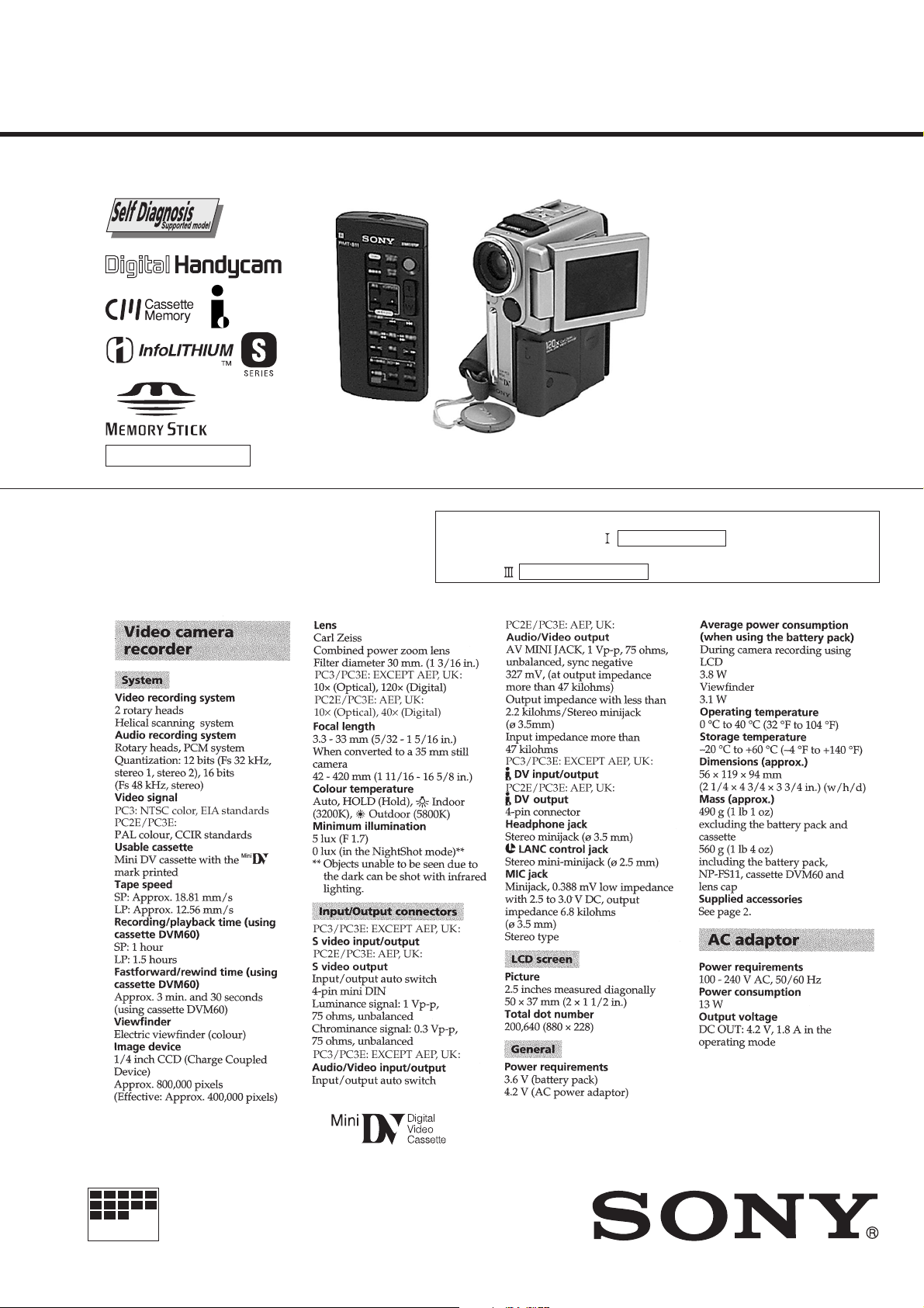
SPECIFICATIONS
Canadian Model
K orea Model
DCR-PC3
AEP Model
UK Model
DCR-PC2E/PC3E
Australian Model
Chinese Model
DCR-PC3E
E Model
Hong Kong Model
Tourist Model
DCR-PC3/PC3E
D MECHANISM ” (original: 9-973-815-
D200 MECHANISM ” (original: 9-973-981-11).
MICROFILM
— Continued on next page —
DIGITAL VIDEO CAMERA RECORDER
DCR-PC2E/PC3/PC3E
4-2. PRINTED WIRING BOARDS AND SCHEMATIC DIAGRAMS
THIS NOTE IS COMMON FOR WIRING BOARDS AND SCHEMATIC DIAGRAMS
(In addition to this, the necessary note is printed in each block)
(For printed wiring boards)
• b: Pattern from the side which enables seeing.
(The other layers' patterns are not indicated.)
• Through hole is omitted.
• Circled numbers refer to waveforms.
• There are few cases that the part printed on diagram
isn’t mounted in this model.
• Chip parts.
Transistor Diode
C
5
BE
64
2
13
5
46
2
31
45
2
31
12
4
53
3
21321321
(For schematic diagrams)
• All capacitors are in mF unless otherwise noted. pF : m mF. 50V
or less are not indicated except for electrolytics and tantalums.
• Chip resistors are 1/10W unless otherwise noted.
kW=1000W, MW=1000kW.
• Caution when replacing chip parts.
New parts must be attached after removal of chip.
Be careful not to heat the minus side of tantalum capacitor, Because it is damaged by the heat.
• Some chip part will be indicated as follows.
Example C541 L452
22U 10UH
TA A 2520
Kinds of capacitor
Temperature characteristics
External dimensions (mm)
• Constants of resistors, capacitors, ICs and etc with XX indicate
that they are not used.
In such cases, the unused circuits may be indicated.
• All v ariable and adjustable resistors hav e characteristic curve B,
unless otherwise noted.
• Signal name
XEDIT→ EDIT PB/XREC → PB/REC
• 2 : non flammable resistor
• 1 : fusible resistor
• C : panel designation
• A : B+ Line
• B : B– Line
• J : IN/OUT direction of (+,–) B LINE.
• C : adjustment for repair.
• Circled numbers refer to waveforms.
Note :
The components identified by
mark ! or dotted line with mark
! are critical for safety.
Replace only with part number
specified.
Note :
Les composants identifiés par
une marque ! sont critiques
pour la sécurité.
Ne les remplacer que par une
pièce portant le numéro spécifié.
(Measuring conditions voltage and waveform)
• Voltages and waveforms are measured between the measurement points and ground when camera shoots color bar chart of
pattern box. They are reference values and reference waveforms.
(VOM of DC 10 MΩ input impedance is used.).
• V oltage values change depending upon input impedance of V OM
used.)
1. Connection
Pattern box
Front of the lens
2. Adjust the distance so that the output waveform of Fig. a and
the Fig. b can be obtain.
Yellow
Cyan
AABBA=B
Fig. a (Video output terminal output waveform)
Cyan
White
Green
Yellow
Fig.b (Picture on monitor TV)
H
White
Green
Red
Magenta
1.5 m
Magenta
Red
Blue
Blue
Electron beam
scanned frame
CRT picture frame
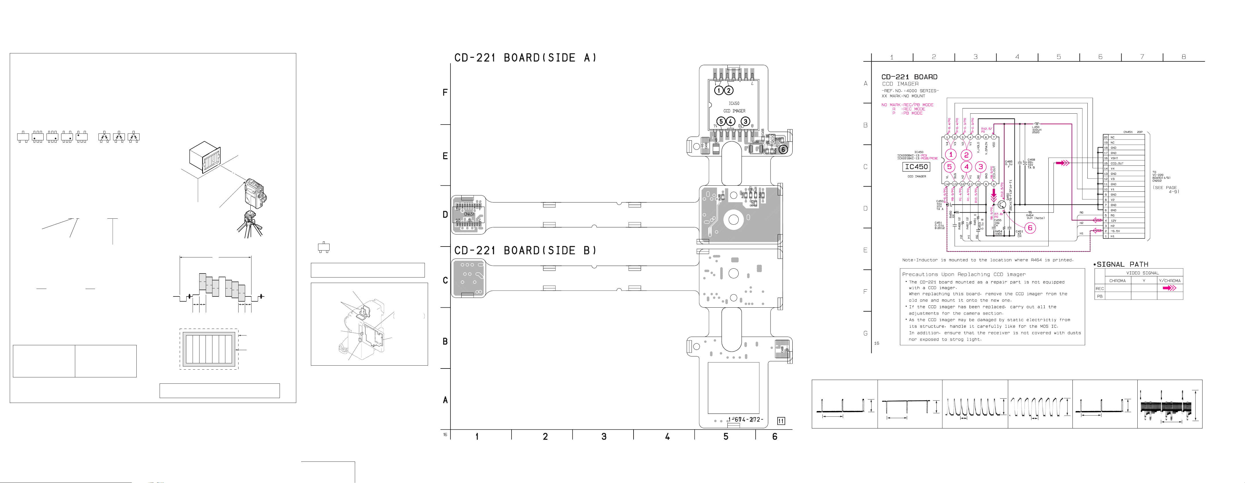
CD-221 BOARD
C450 E-5
C451 E-5
C453 D-5
C455 E-6
C461 E-5
C465 E-6
C468 B-6
CN451 D-1
IC450 F-5
L450 E-5
Q450 E-6
R450 D-5
R451 D-5
R454 E-6
R464 D-6
R466 D-5
R467 D-5
For printed wiring boards
• This board is six-layer print board. However, the patterns of layers two to five have not been included in
the diagram.
• Chip parts
Transistor
C
BE
There are few cases that the part printed on this
diagram isn’t mounted in this model.
VF-136
(BACK-LIGHT DRIVE)
CD-221
(CCD IMAGER)
PD-112
RGB DECODER,
TIMING GENERATOR
PR-32
(PANEL REVERSE)
INVERTER
TRANSFORMER UNIT
PO-4
(PANEL OPEN)
CD-221 (CCD IMAGER) PRINTED WIRING BOARD
— Ref. No. CD-221 Board; 4,000 Series —
CD-221
CAMERA REC
BOARD
When indicating parts by reference number, pleas include
1
IC450 1,2
2
IC450 3,4
3
IC450 !º
4
IC450 !¡,!™
the board name.
H
6.8Vp-p
H
6.8Vp-p
56nsec
2.7Vp-p
56nsec
3Vp-p
CCD IMAGER
4-5 4-6 4-7 4-8
CD-221
5
IC450 !£
H
17Vp-p
6
Q450 E
0.96Vp-p
H
For schematic diagram
• Refer to page 4-37 for printed wiring board.
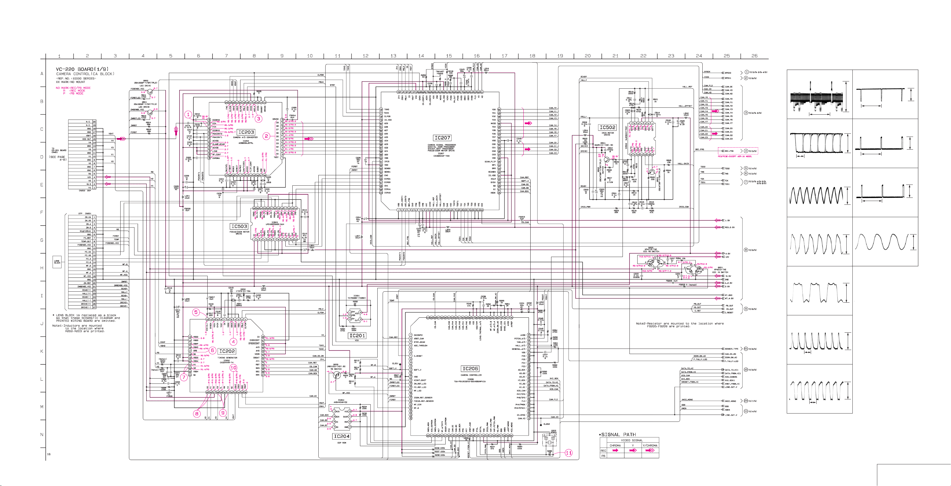
VC-220
CAMERA REC
1
IC203 @§,@¶
BOARD (1/9)
DCR-PC2E/PC3/PC3E
8
IC202 @∞,@§
H
2
IC203 2-!¡
56nsec
3
IC203 !§
CAMERA REC/PB
18MHz
4
IC202 5
CAMERA REC/PB
36.0MHz
0.96Vp-p
2.7Vp-p
2.7Vp-p
3.0Vp-p
H
9
IC202 @•,#¡
H
!º
IC202 #£
H
!¡
IC206 $º (X202)
CAMERA REC/PB
20.0MHz
7.0Vp-p
7Vp-p
19Vp-p
2.6Vp-p
5
IC202 !™
CAMERA REC/PB
18.0MHz
6
IC202 !•
56nsec
7
IC202 @¡,@™
56nsec
2.7Vp-p
2.7Vp-p
2.8Vp-p
4-9 4-10 4-11
CAMERA CONTROL
VC-220 (1/9)
DCR-PC2E/PC3/PC3E
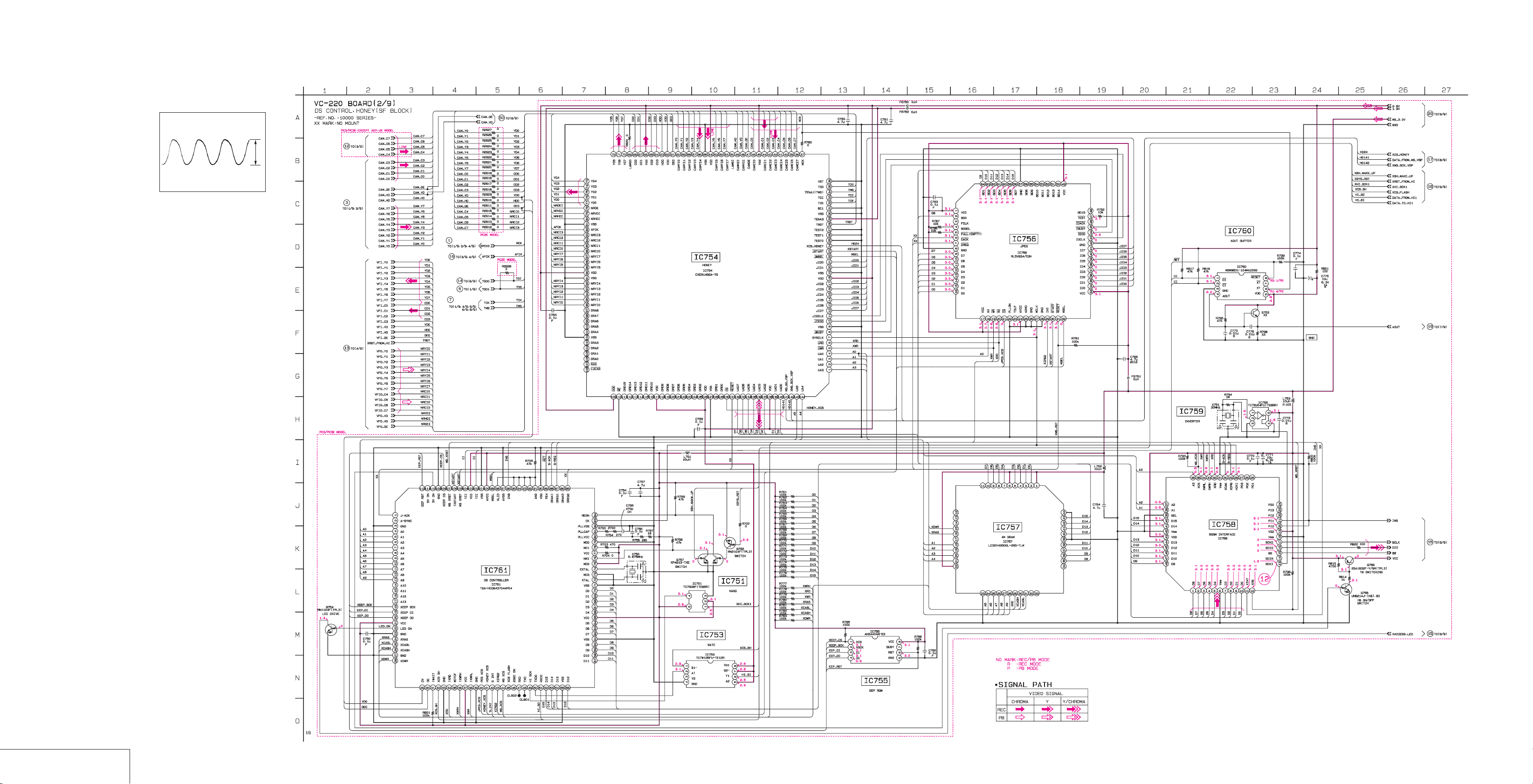
VC-220
CAMERA REC/PB
!™
BOARD (2/9)
IC758 !£
For schematic diagram
• Refer to page 4-37 for printed wiring board.
20MHz
3.2Vp-p
DS CONTROL • HONEY
VC-220 (2/9)
4-12 4-13 4-14
For schematic diagram
• Refer to page 4-37 for printed wiring board.
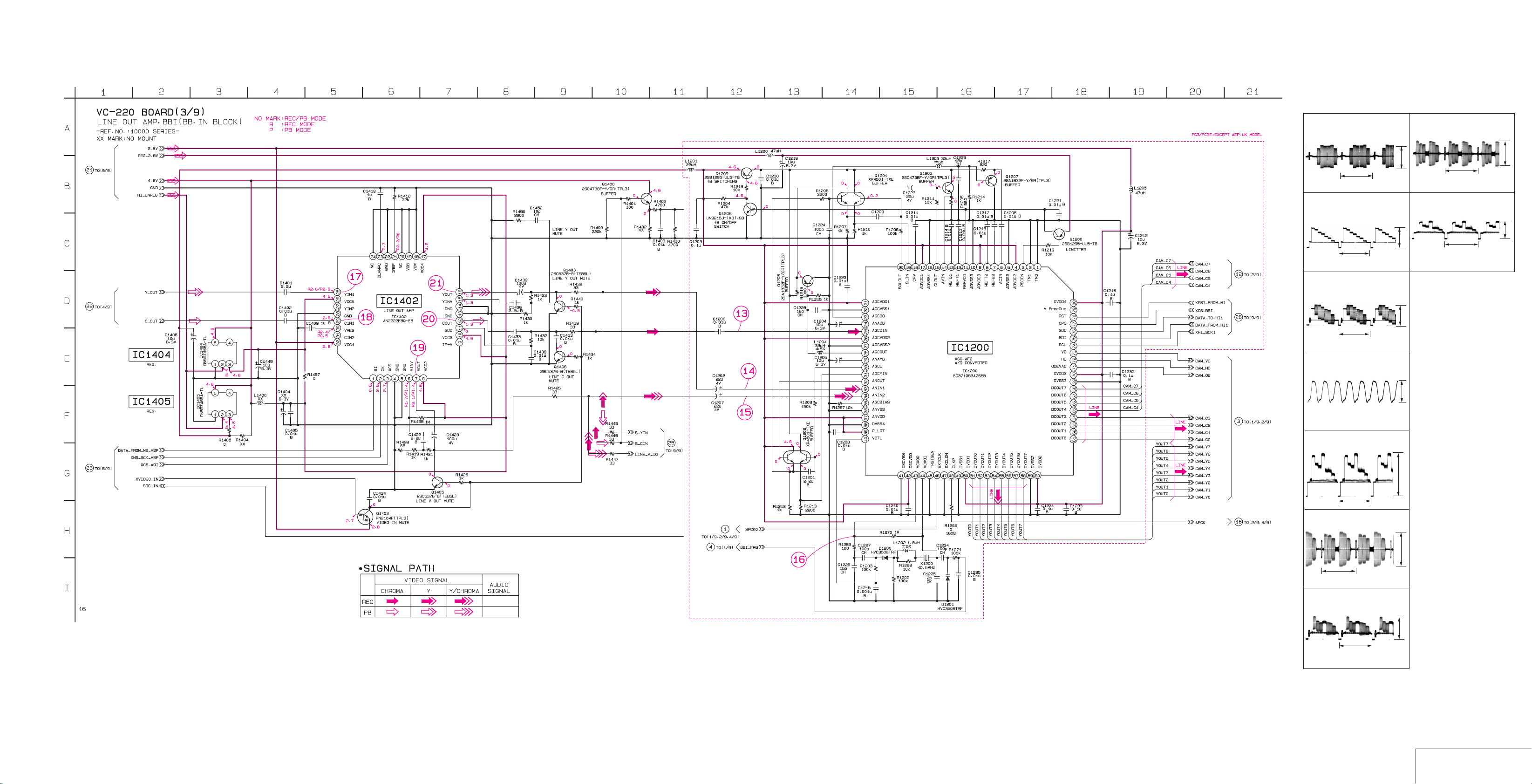
VC-220
CAMERA REC/PB
!£
LINE REC
BOARD (3/9)
IC1200 @∞
(C1200)
DCR-PC2E/PC3/PC3E
@º
IC1402 !™
!¢
IC1200 #£
LINE REC
!∞
IC1200 #¢
LINE REC
!§
IC1200 $£
LINE REC
40.5MHz
H
(C1202)
H
(C1207)
H
(R1270)
0.44Vp-p
0.37Vp-p
0.46Vp-p
4Vp-p
@¡
IC1402 !§
H
H
1.4Vp-p
1.7Vp-p
!¶
!•
!ª
IC1402 @∞
IC1402 @ª
H
IC1402 7
0.45Vp-p
H
0.34Vp-p
H
1.9Vp-p
4-15 4-16 4-17
LINE OUT AMP, BBI
VC-220 (3/9)
DCR-PC2E/PC3/PC3E
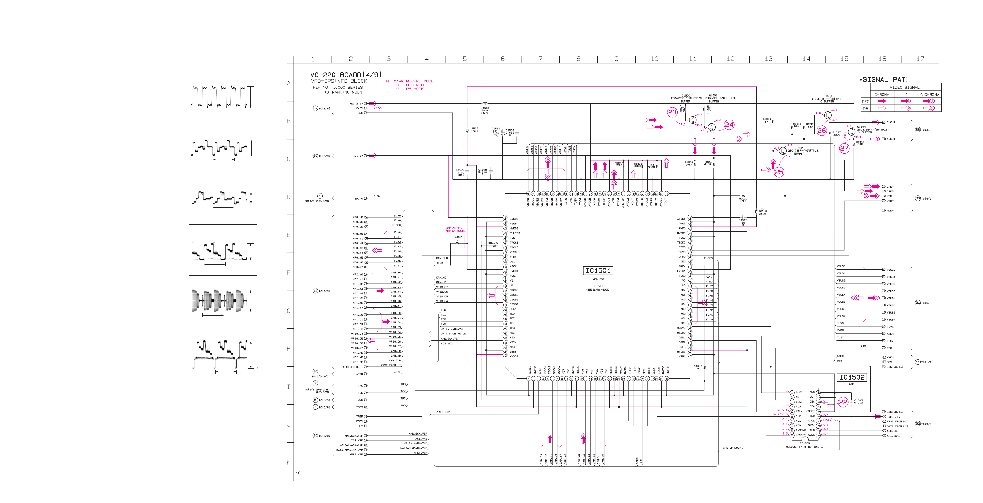
VC-220
CAMERA REC/PB
@™
BOARD (4/9)
IC1502 8
For schematic diagram
• Refer to page 4-37 for printed wiring board.
@£
@¢
@∞
@§
13.5MHz
Q1500 E
Q1501 E
Q1502 E
H
Q1503 E
3.0Vp-p
0.22Vp-p
H
H
0.2Vp-p
0.26Vp-p
VFD-CPS
VC-220 (4/9)
0.32Vp-p
0.4Vp-p
H
@¶
H
Q1504 E
4-18 4-19 4-20
 Loading...