

Sony CDXCA-860-X Service manual
CDX-CA850/CA850X/CA860X
SERVICE MANUAL
Ver 1.3 2001. 09
Photo: CDX-CA850X
• The tuner and CD sections have no adjustments.
AUDIO POWER SPECIFICATIONS (US Model)
POWER OUTPUT AND TOTAL HARMONIC DISTORTION
23.2 watts per channel minimum continuous average power into
4 ohms, 4 channels driven from 20 Hz to 20 kHz with no more
than 5% total harmonic distortion.
CD player section
Signal-to-noise ratio 90 dB
Frequency response 10 – 20,000 Hz
Wow and flutter Below measurable limit
Laser Diode Properties (US, Canadian Model)
Material GaAlAs
Wavelength 780 nm
Emission Duration Continuous
Laser output power Less than 44.6 µW*
* This output is the value measured at a distance
of 200 mm from the objective lens surface on the
Optical Pick-up Block.
Tuner section
FM
Tuning range 87.5 – 107.9 MHz (US, Canadian model)
87.5 – 108.0 MHz (AEP, UK model)
Antenna terminal External Antenna connector
Intermediate frequency 10.7 MHz/450 kHz
Usable sensitivity 8 dBf
Selectivity 75 dB at 400 kHz
Signal-to-noise ratio 66 dB (stereo),
72 dB (mono)
Harmonic distortion at 1 kHz
0.6% (stereo),
0.3% (mono)
Separation 35 dB at 1 kHz
Frequency response 30 – 15,000 Hz
AM (US, Canadian model)
Tuning range 530 – 1,710 kHz (US, Canadian model)
Antenna terminal External Antenna connector
Intermediate frequency 10.7 MHz/450 kHz
Sensitivity 30 µV
MW/LW (AEP, UK model)
Tuning range MW: 531 – 1,602 kHz
LW: 153 – 279 kHz
Aerial terminal External Aerial connector
Intermediate frequency 10.7 MHz/450 kHz
Sensitivity MW: 30 µV
LW: 40 µV
SPECIFICATIONS
FM/MW/LW COMPACT DISC PLAYER
US Model
Canadian Model
CDX-CA850X/CA860X
AEP Model
UK Model
CDX-CA850
Model Name Using Similar Mechanism CDX-C5000R
CD Drive Mechanism Type MG-383Z-121//Q
Optical Pick-up Name KSS-720A
Power amplifier section
Outputs Speaker outputs
(sure seal connectors)
Speaker impedance 4 – 8 ohms
Maximum power output 52 W × 4 (at 4 ohms)
General
Outputs Audio outputs (front/rear)
Subwoofer output (mono)
Power Antenna relay control lead
Power amplifier control lead
Inputs Telephone ATT control lead
Illumination control lead
Bus control input connector
Bus audio input connector
Remote controller input connector
Antenna input connector
Tone controls Bass ±10 dB at 62 Hz (US, Canadian model)
Bass ±8 dB at 100 Hz (AEP, UK model)
Treble ±10 dB at 16 kHz (US, Canadian model)
Treble ±8 dB at 10 kHz (AEP, UK model)
Loudness +8 dB at 100 Hz
+2 dB at 10 kHz
Power requirements 12 V DC car battery
(negative ground)
– Continued on next page –
CDX-CA850
FM/AM COMPACT DISC PLAYER
CDX-CA850X/CA860X
9-870-291-14
2001I0400-1
© 2001. 9
Sony Corporation
e Vehicle Company
Shinagawa Tec Service Manual Production Group
1
CDX-CA850/CA850X/CA860X
k
Dimensions Approx. 178 × 50 × 177 mm
(7 1/8 × 2 × 7 in.) (w/h/d)
Mounting dimensions Approx. 182 × 53 × 162 mm
(7 1/4 × 2 1/8 × 6 1/2 in.) (w/h/d)
Mass Approx. 1.3 kg
(2 lb. 10 oz.)
Supplied accessories Parts for installation and connections (1 set)
Front panel case (1)
Rotary commander
RM-X5S
Card remote commander
RM-X112 (CDX-CA850X/CA860X)
RM-X113 (CDX-CA850)
Note
This unit cannot be connected to a digital preamplifier or an equalizer.
Design and specifications are subject to change without
notice.
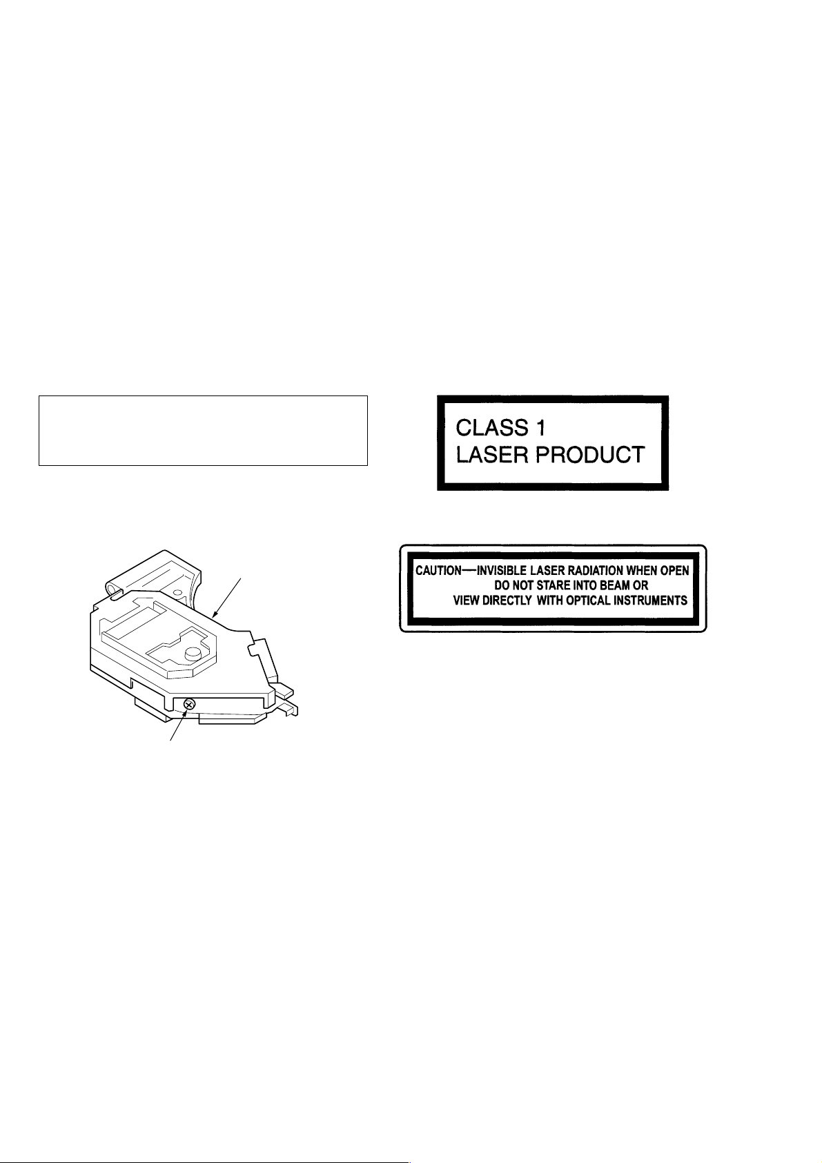
SERVICE NOTES
• US, Canadian model
CAUTION
Use of controls or adjustments or performance of procedures
other than those specified herein may result in hazardous
radiation exposure.
If the optical pick-up block is defective, please replace the whole
optical pick-up block.
Never turn the semi-fixed resistor located at the side of optical
pick-up block.
• AEP, UK model
This label is located on the bottom of the chassis.
optical pick-up bloc
semi-fixed resistor
NOTES ON HANDLING THE OPTICAL PICK-UP BLOCK
OR BASE UNIT
The laser diode in the optical pick-up block may suffer electrostatic
breakdown because of the potential difference generated by the
charged electrostatic load, etc. on clothing and the human body.
During repair, pay attention to electrostatic breakdown and also use
the procedure in the printed matter which is included in the repair
parts.
The flexible board is easily damaged and should be handled with
care.
This label is located on the drive unit's internal
chassis.
When replacing the chassis (T .U) of mechanism deck which have
the “CAUTION LABEL” attached, please be sure to put a new
CAUTION LABEL (3-223-913-11) to the chassis (T.U).
NOTES ON LASER DIODE EMISSION CHECK
The laser beam on this model is concentrated so as to be focused on
the disc reflective surface by the objective lens in the optical pickup block. Therefore, when checking the laser diode emission, observe from more than 30 cm away from the objective lens.
Notes on Chip Component Replacement
• Never reuse a disconnected chip component.
• Notice that the minus side of a tantalum capacitor may be dam-
aged by heat.
SAFETY-RELATED COMPONENT WARNING!!
COMPONENTS IDENTIFIED BY MARK 0 OR DOTTED LINE
WITH MARK 0 ON THE SCHEMATIC DIAGRAMS AND IN
THE PARTS LIST ARE CRITICAL TO SAFE OPERATION.
REPLACE THESE COMPONENTS WITH SONY P ARTS WHOSE
PART NUMBERS APPEAR AS SHOWN IN THIS MANUAL OR
IN SUPPLEMENTS PUBLISHED BY SONY.
2
ATTENTION AU COMPOSANT AYANT RAPPORT
À LA SÉCURITÉ!!
LES COMPOSANTS IDENTIFIÉS P AR UNE MARQUE 0 SUR LES
DIAGRAMMES SCHÉMATIQUES ET LA LISTE DES PIÈCES
SONT CRITIQUES POUR LA SÉCURITÉ DE FONCTIONNEMENT.
NE REMPLACER CES COMPOSANTS QUE PAR DES PIÈCES
SONY DONT LES NUMÉROS SONT DONNÉS DANS CE MANUEL
OU DANS LES SUPPLÉMENTS PUBLIÉS PAR SONY.

TABLE OF CONTENTS
CDX-CA850/CA850X/CA860X
Ver 1.1 2001. 04
1. GENERAL
........................................................................... 4
2. DISASSEMBLY
2-1. Sub Panel Assy.................................................................. 10
2-2. CD Mechanism Block ....................................................... 10
2-3. Main Board ....................................................................... 10
2-4. Heat Sink ........................................................................... 11
2-5. Chassis (T) Assy................................................................ 11
2-6. Lever Section..................................................................... 12
2-7. Servo Board....................................................................... 12
2-8. Arm Roller Assy ................................................................ 13
2-9. Chassis (OP) Assy.............................................................13
2-10. Optical Pick-up Block ....................................................... 14
3. DIAGRAMS
3-1. IC Pin Descriptions ........................................................... 15
3-2. Block Diagram –CD Section–........................................... 23
3-3. Block Diagram –Tuner Section–....................................... 24
3-4. Block Diagram –Display Section–....................................25
3-5. Circuit Boards Location .................................................... 26
3-6. Printed Wiring Boards –CD Mechanism Section–............ 28
3-7. Schematic Diagram –CD Mechanism Section (1/2)– ....... 30
3-8. Schematic Diagram –CD Mechanism Section (2/2)– ....... 31
3-9. Printed Wiring Boards –Main Section– ............................ 32
3-10. Schematic Diagram –Main Section (1/4)– ........................ 34
3-11. Schematic Diagram –Main Section (2/4)– ........................ 35
3-12. Schematic Diagram –Main Section (3/4)– ........................ 36
3-13. Schematic Diagram –Main Section (4/4)– ........................ 37
3-14. Printed Wiring Board –Sub (CD) Section–....................... 38
3-15. Schematic Diagram –Sub (CD) Section–.......................... 39
3-16. Printed Wiring Board –Key Section–................................ 40
3-17. Schematic Diagram –Key Section–................................... 41
4. EXPLODED VIEWS
4-1. Chassis Section ................................................................. 46
4-2. Front panel Section ........................................................... 47
4-3. CD Mechanism Section (1) ............................................... 48
4-4. CD Mechanism Section (2) ............................................... 49
4-5. CD Mechanism Section (3) ............................................... 50
5. ELECTRICAL PARTS LIST ........................................ 51
3
CDX-CA850/CA850X/CA860X
SECTION 1
GENERAL
This section is extracted from AEP,
UK model’s instruction manual.
4
CDX-CA850/CA850X/CA860X
5
CDX-CA850/CA850X/CA860X
6
CDX-CA850/CA850X/CA860X
7
CDX-CA850/CA850X/CA860X
8
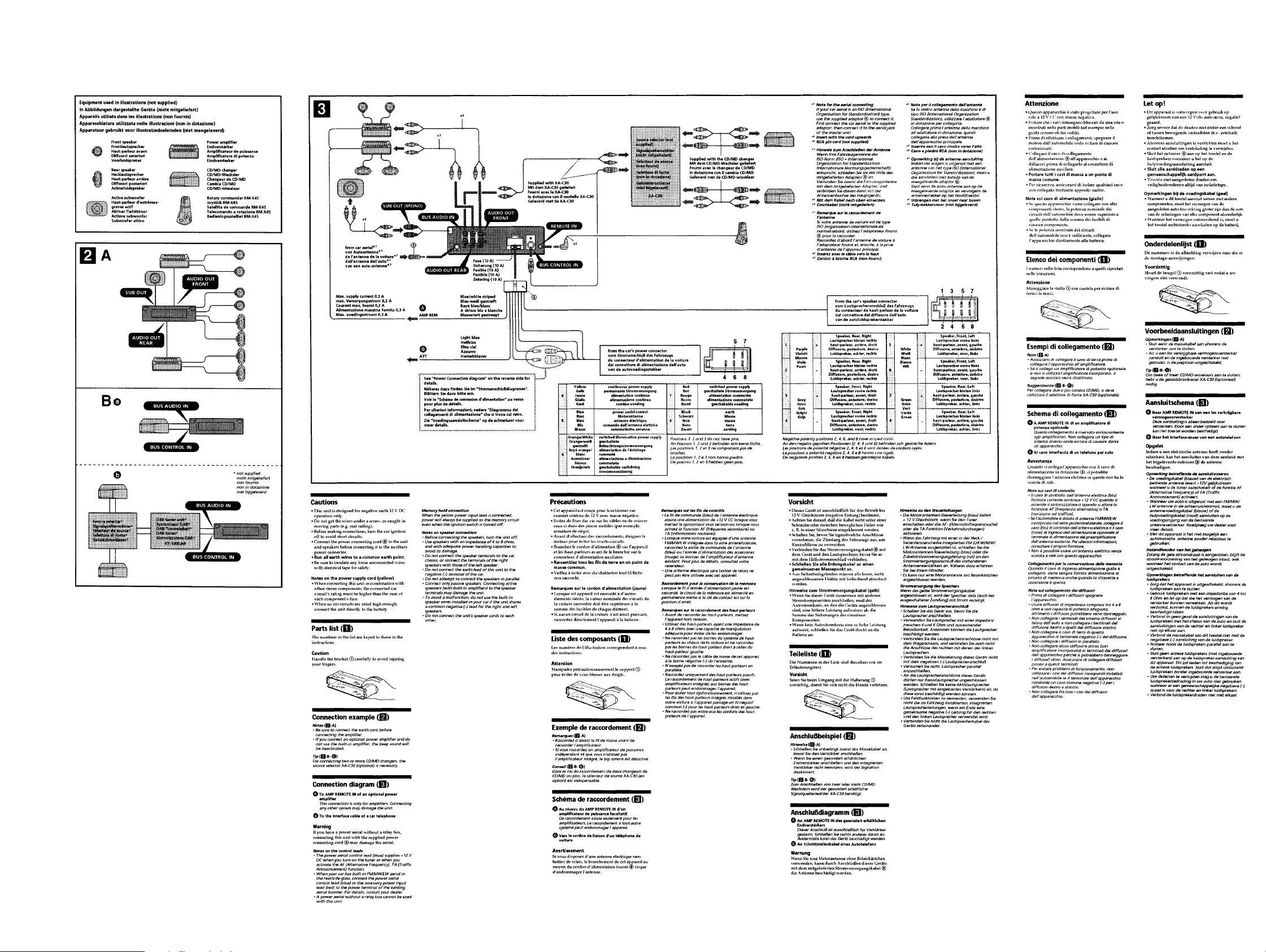
Connection
CDX-CA850/CA850X/CA860X
99
CDX-CA850/CA850X/CA860X
4
4
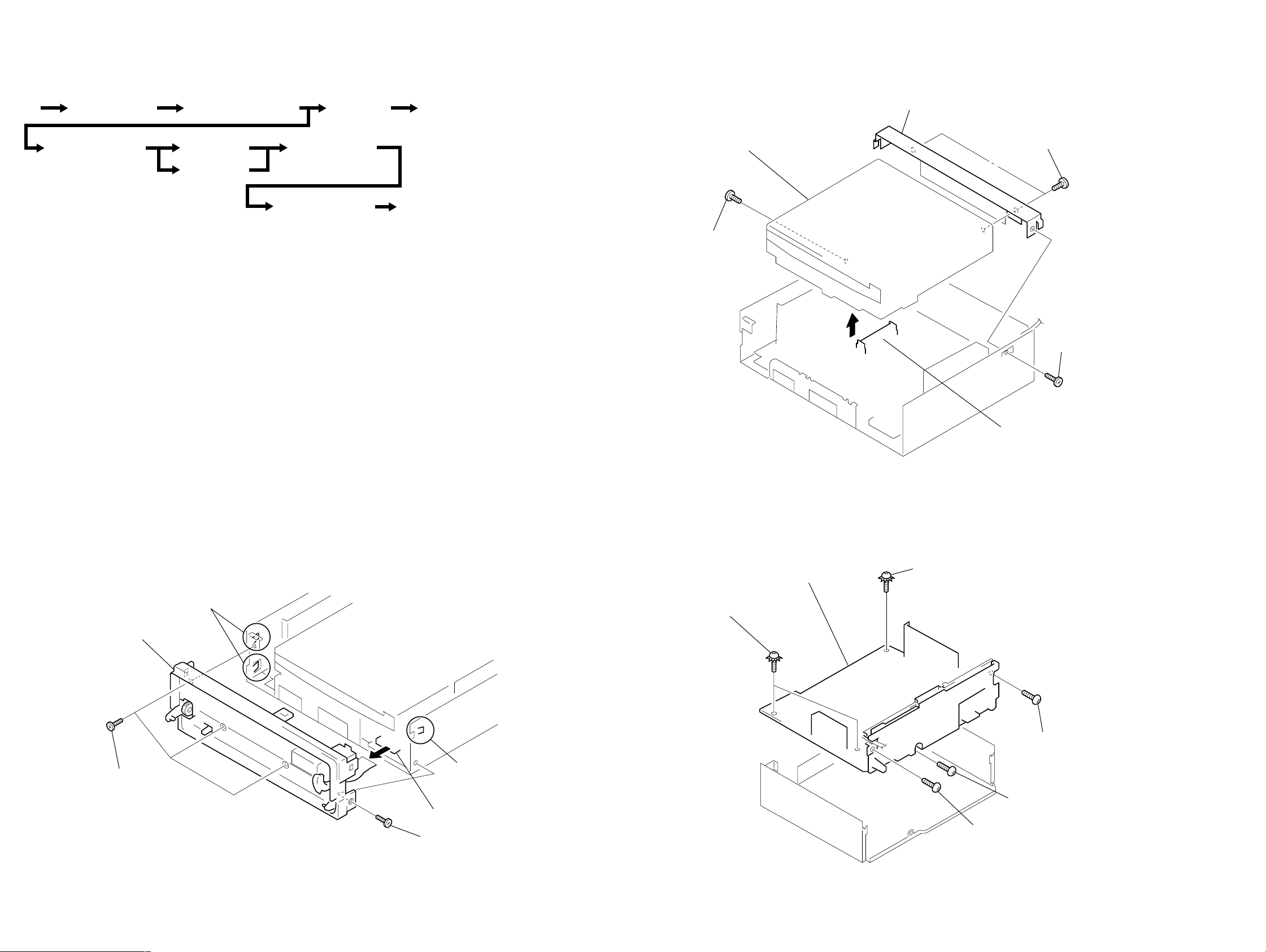
SECTION 2
DISASSEMBLY
Note : This equipment can be removed using the following procedure.
Set Sub Panel Assy CD Mechanism Block
Chassis (T) Assy lever Section
Servo Board
Chassis (OP) Assy Optical Pick-up Block
Main Board Heat Sink
Arm Roller Assy
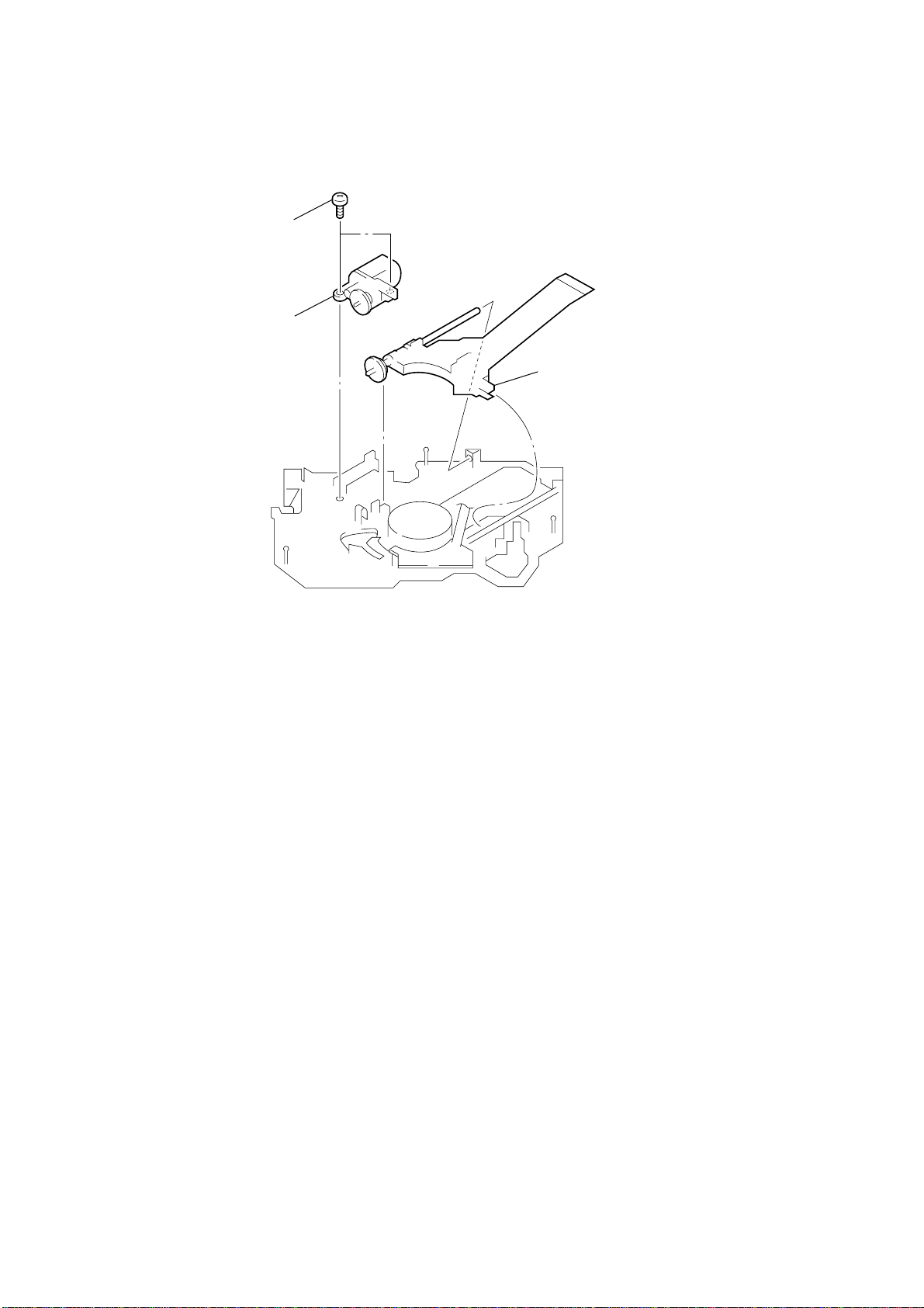
2-2. CD MECHANISM BLOCK
5 CD mechanism block
2 PTT 2.6x4
7 bracket (CD)
6 PTT 2.6x4
3
1 PTT 2.6x
Note : Follow the disassembly procedure in the numerical order given.
2-1. SUB PANEL ASSY
4 two claws
6 sub panel assy
2-3. MAIN BOARD
6 MAIN board
5 ground point screws
(PTT 2.6x6)
4 CN401
4 ground point screw
(PTT 2.6x6)
3 PTT 2.6x
2 PTT 2.6x6
3 claw
2 PTT 2.6x4
5 CN701
1 PTT 2.6x6
1 PTT 2.6x4
1010
0
2-4. HEAT SINK
CDX-CA850/CA850X/CA860X
5 heat sink
3 PTT 2.6x1
2-5. CHASSIS (T) ASSY
1 Unsolder the
lead wires.
2 PTT 2.6x16
1 PTT 2.6x10
4 PTT 2.6x4
2 P 2x3
3 P 2x3
4 chassis (T) assy
black
red
white
11
CDX-CA850/CA850X/CA860X
2-6. LEVER SECTION
5
6
lever (R) sub assy
3
tension spring (LR)
7
lever (L) sub assy
guide (disc)
1
PS 2x4
2
DISC IN board
2-7. SERVO BOARD
8 loading motor assy
(M903)
4
claws
9 PS 2x4
5 Removal the solders.
3 CN3
7 P 2x3
1 PS 2x5
2 heat sink (CD)
7 PS 2x4
4 CN2
0 SERVO board
6 Removal the solders.
12
3 PS 2x3
4 LOAD board
1 tension spring (RA2)
2 arm roller assy
Fig. 1
retaining ring (roller)
arm
arm
washer(RA)
washer(RA)
bearing (roller)
bearing (roller)
2-8. ARM ROLLER ASSY
• When installing, take note of the positions
arm (roller) and washers. (Fig. 1)
CDX-CA850/CA850X/CA860X
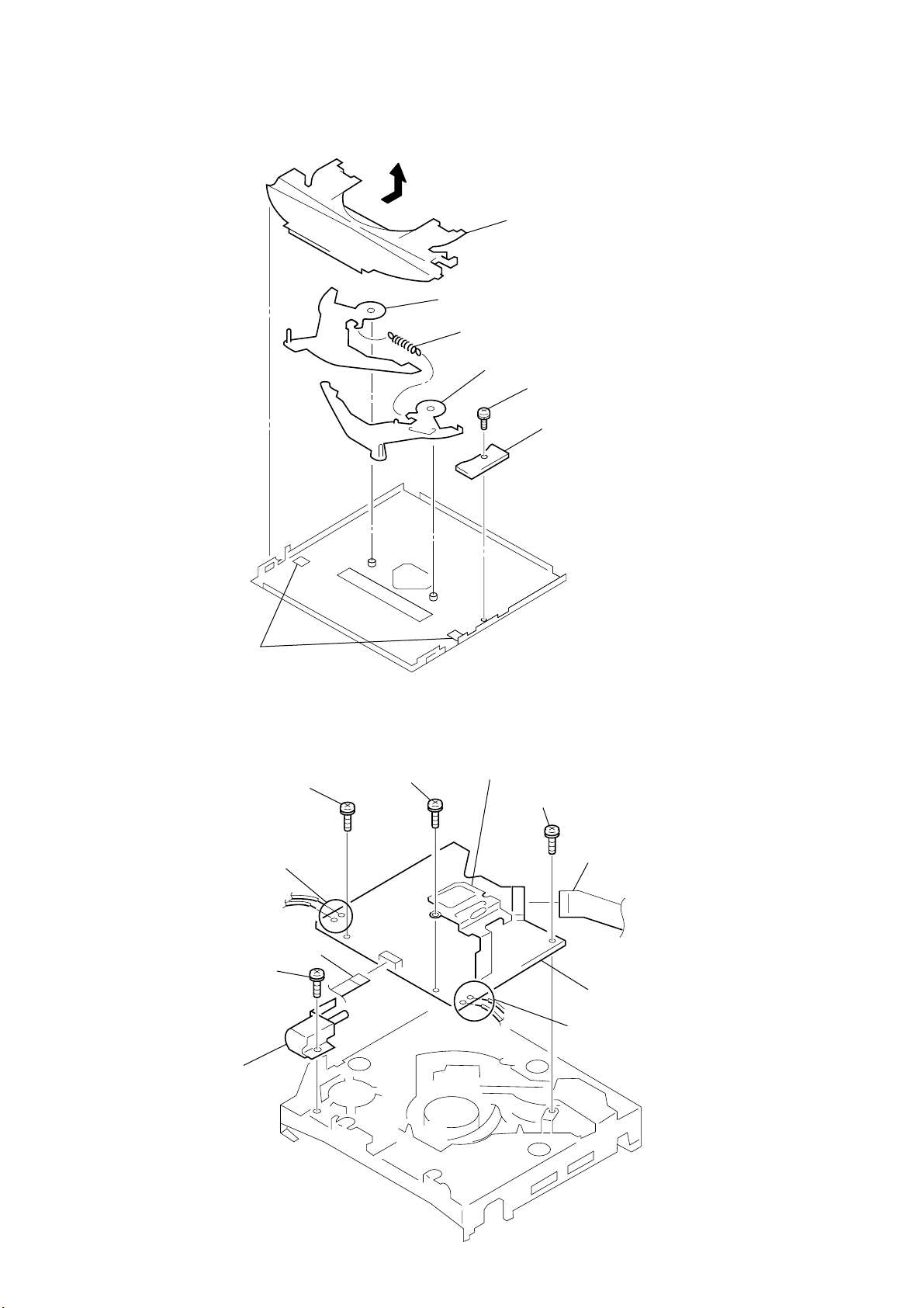
2-9. CHASSIS (OP) ASSY
8 compression spring (FL)
1 tension spring (KF1)
9 compression spring (FL)
2 tension spring (KR1)
7 chassis (OP) assy
5 Fit lever (D) in the
direction of the arrow.
6 Turn loading ring in the
direction of the arrow.
4 damper (T)
3 damper (T)
13
CDX-CA850/CA850X/CA860X
2-10. OPTICAL PICK-UP BLOCK
1 P 2x3
2 sled motor assy
(M902)
3 optical pick-up block
14
CDX-CA850/CA850X/CA860X
SECTION 3
DIAGRAMS
3-1. IC PIN DESCRIPTIONS
• IC501 CXD2598Q (DIGITAL SER VO, DIGITAL SIGNAL PROCESSOR) (SERVO BOARD)
Pin No. Pin Name I/O Pin Description
1 DVDD — Digital power supply pin
2 DVSS — Digital ground
3 SOUT O Servo brock serial data output (Not used.)
4 SOCK O Servo brock serial data read clock output (Not used.)
5 XOLT O Servo brock serial data latch output (Not used.)
6 SQSO O Sub Q 80 bit, PCM peak and level data output. CD TEXT data output
7 SQCK I Clock input from SQSO read output.
8 SCSY I Fixed at “L”.
9 SBSO O Serial output of sub-P to W. (Not used.)
10 EXCK I Clock input from SBSO read output. (Fixed at “L”)
11 XRST I System reset (“L”: Reset)
12 STSM I System mute input (Fixed at “L”)
13 DATA I Serial data input from CPU.
14 XLAT I Latch input from CPU. Latch serial data at the falling edge.
15 CLOK I Serial data transfer clock input from CPU.
16 SENS O SENS output for CPU.
17 SCLK I Clock input from SENS serial data read.
18 ATSK I/O Input/output for anti-shock.
19 WFCK O WFCK (Write Flame Clock) output (Not used.)
20 XUGF O XUGF output (Not used.)
21 XPCK O XPCK output (Not used.)
22 GFS O GFS output
23 C2PO O C2PO output (Not used.)
24 SCOR O “H” output at either detection, sub code sync S0 or S1.
25 C4M O 4.2336 MHz output (Not used.)
26 WDCK O Word clock input f=2Fs (Not used.)
27 COUT I/O Track number count signal input/output (Not used.)
28 MIRR I/O Mirror signal input/output (Not used.)
29 DVSS — Digital ground
30 DVDD — Digital power supply pin
31 DFCT I/O Diffect signal input/output (Not used.)
32 FOK I/O Focus OK signal output
33 PWM1 I External control input of spindle motor.
34 LOCK I/O Lock signal input/output
35 MDP O Servo control output of spindle motor.
36 SSTP I Disc most inner track detection signal input
37 FSTIO I/O 2/3 frequency division output of pins ih and ij. (Not used.)
38 SFDR O Sled drive output
39 SRDR O Sled drive output
40 TFDR O Tracking drive output
41 TRDR O Tracking drive output
42 FFDR O Focus drive output
43 FRDR O Focus drive output
44 DVDD — Digital power supply pin
45 DVSS — Digital ground
46 TEST I Test pin (Fixed at “L”)
47 TES1 I Test pin (Fixed at “L”)
48 XTSL I X’tal select input (“L”: 16.9344 MHz, “H”: 33.8688 MHz)
49 VC I Center voltage input
50 FE I Focus error signal input
51 SE I Sled error signal input
15

CDX-CA850/CA850X/CA860X
Pin No. Pin Name I/O Pin Description
52 TE I Tracking error signal input
53 CE I Center servo analog input
54 RFDC I RF signal input
55 ADIO O Test pin (Not used.)
56 AVSSO — Analog ground
57 IGEN I Constant current input from OP amplifier.
58 AVDDO — Analog ground
59 ASYO O EFM full-swing output (“L”: VSS, “H”: VDD)
60 ASYI I Asymmetry comparate voltage input
61 RFAC I EFM signal input
62 AVSS3 — Analog ground
63 CLTV I VCO control voltage input from master.
64 FILO O Filter output for master PLL (slave=digital PLL)
65 FILI I Filter input from master PLL.
66 PCO O Charge pump output for master PLL.
67 AVDD3 — Analog power supply pin
68 BIAS I Asymmetry circuit constant current input
69 VCTL I VCO2 control input from wideband EFM PLL. (Not used.)
70 V16M O VCO2 oscillator output for wideband EFM PLL. (Not used.)
71 VPCO O Charge pump output for wideband EFM PLL. (Not used.)
72 DVSS — Digital ground
73 MD2 I Digital out ON/OFF control input (“L”: OFF, “H”: ON)
74 DOUT O Digital out output
75 ASYE I Asymmetry circuit ON/OFF input (“L”: OFF, “H”: ON)
76 DVDD — Digital power supply pin
77 LRCK O D/A interface LR clock output (f=Fs)
78 LRCKI I D/A interface LR clock input
79 PCMD O D/A interface serial data output (2’s COMP, MSB fast)
80 PCMDI I D/A interface serial data input (2’s COMP, MSB fast)
81 BCK O D/A interface bit clock output
82 BCKI I D/A interface bit clock input
83 EMPH O Emphasis ON/OFF signal output
84 EMPHI I Emphasis ON/OFF signal input (“H”: ON, “L”: OFF)
85 XVDD — Power supply for master clock.
86 XTAI I X’tal oscillator input from master clock (16.9344 MHz).
87 XTAO O X’tal oscillator output for master clock (16.9344 MHz).
88 XVSS — Ground pin for master clock.
89 AVDD1 — Analog power supply pin
90 AOUT1 O Lch analog output
91 AIN1 I Lch OPAMP input
92 LOUT1 O Lch LINE output
93 AVSS1 — Analog ground
94 AVSS2 — Analog ground
95 LOUT2 O Rch LINE output
96 AIN2 I Rch OPAMP input
97 AOUT2 O Rch analog output
98 AVDD2 — Analog power supply pin
99 RMUT O Rch “0” detect Flug (Not used.)
100 LMUT O Lch “0” detect Flug (Not used.)
16
CDX-CA850/CA850X/CA860X
• IC5 CXP84640-072Q (CD SYSTEM CONTROL) (SERVO BOARD)
Pin No. Pin Name I/O Pin Description
1 ITRPT — Not used in this set.
2, 3 — — Not used in this set.
4, 5 NCO — Not used in this set.
6 OPEN I Front panel open detection input
7 CLOSE O Front panel close control output
8 LINKOFF I Bus interface link input
9 NCO — Not used in this set.
10 D SW I Down switch input (SW4)
11 SSTP I Limit switch input (SW3)
12, 13 NCO — Not used in this set.
14, 15 — — Not used in this set.
16 EMPH O O De-emphasis ON/OFF control output
17 CDMON O CD mechanism deck power control output
18 CD ON O CD power control output
19 A MUT O System attenuate control output
20 LD ON O Laser power ON/OFF control output
21 CD RST O CD system reset output
22 HOLD O Hold switch output
23 AGC CONT O AGC control output
24 — — Not used in this set.
25 PH3 I Not used in this set.
26 TSTIN0 I Not used in this set.
27 TSTIN1 I Not used in this set.
28 TST.CLV I Not used in this set.
29 NCO — Not used in this set.
30 RESET I System reset input (“L”=Reset)
31 X IN I X’tal oscillator input from system clock. (10 MHz)
32 X OUT O X’tal oscillator output for system clock. (10 MHz)
33 GND — Analog ground
34 XT OUT O Not used in this set.
35 XT IN I Not used in this set.
36 AVSS — A/D converter ground
37 AVREF I A/D converter reference voltage input
38 TEP L I Not used in this set.
39 TEP H I Not used in this set.
40 SLED– I Sled drive input
41 PH2 I Not used in this set.
42 SEK/SMET I Fixed at “H” in this set.
43 GFS/MNT2 SEL I Fixed at “H” in this set.
44 SC-JIG ON/OFF I Fixed at “H” in this set.
45 SCLK O CD-TEXT data read clock output
46 LOCK I/O Lock signal input/output
47 — — Not used in this set.
48 SCK2 O Sub Q read clock output
49 SI2 I Sub Q 80 bit, PCM peak and level data 16 bit input.
50 — — Not used in this set.
51 BUS CLK I/O Bus system serial clock input/output
52 BUS SI I Bus system serial interface input
53 BUS SO O Bus system serial interface output
54 F OK I Focus OK signal input
55 GFS I GFS signal detection input
56 TEST MODE I Fixed at “H” in this set.
17
CDX-CA850/CA850X/CA860X
Pin No. Pin Name I/O Pin Description
57 SENS I SENS signal input
58 — — Not used in this set.
59 — — Not used in this set.
60 BU.IN I Back-up power detection input
61 BUSON I Bus on control input
62 IN SW I Disc in switch input (SW1)
63 SELF SW I Self switch input (SW2)
64 SCOR O Sub-code sync output
65 CD-CKO O CD signal process serial clock input
66 LM LOD O Loading motor control output
67 CD DATA O CD signal process serial data output
68 CD-XLAT O CD signal process serial data latch output
69 LM-EJ O Loading motor control output
70 DRV-OE O Focus/tracking coil/sled motor control output
71 MD2 O Digital out ON/OFF control output (“L”: OFF, “H”: ON)
72 VDD — Power supply pin
73 NIH I Fixed at “H” in this set.
74 V/Z I Fixed at “H” in this set.
75 PH1 I Not used in this set.
76 — — Not used in this set.
77 DOUT-SEL I Fixed at “H” in this set.
78 – 80 — — Not used in this set.
18
CDX-CA850/CA850X/CA860X
• IC501 MB90574BPMT-G-323-BND (MAIN SYSTEM CONTROL) (CDX-CA850X/CA860X) (MAIN BOARD)
• IC501 MB90574BPMT-G-324-BND (MAIN SYSTEM CONTROL) (CDX-CA850) (MAIN BOARD)
Pin No. Pin Name I/O Pin Description
1 – 4 NCO O Not used. (Open)
5 ATT O System mute control signal output
6, 7 NCO O Not used. (Open)
8 VCC — Power supply pin (+5 V)
9 AMP ATT O Amp mute signal output
10 E2PSIO I/O EEPROM data signal input/output
11 E2PCKO O EEPROM clock signal output
12 DOOR SW/FLS SI I Door switch signal input (L: close) Flash write data signal input
13 FLS SO O Flash write data signal output
14 BUS ON O BUS ON control signal output
15 BEEP O Beep signal output
16 NS MASK O Tuner mute signal output
17 UNISI I SONY BUS data signal input
18 UNISO O SONY BUS data signal output
19 UNICKO O SONY BUS clock signal output
20 IFWIDTH O Not used. (Open)
21 SWSHIFT O Not used. (Open)
22 SYSRST O System reset signal output
23 (NCO) O Not used. (Open)
24 SIRCS I Remote control data signal input
25 – 29 NCO O Not used. (open)
30 AMPON O Amp on signal output (L: OFF/H: ON)
31 VOLATT O Electronic volume mute signal output (L: Mute on)
32 NCO O Not used. (Open)
33 VSS — Ground pin
34 C — Power stabilized capacitance pin Not used. (open)
35 – 37 NCO O Not used. (Open)
38 DVCC — D/A converter VREF input
39 DVSS — D/A converter GND pin
40, 41 (NCO) O Not used. (Open)
42 AVCC — Analog power supply pin (+5 V)
43 AVRH — A/D converter VREF+ input
44 AVRL — A/D converter VREF– input
45 AVSS — Analog ground pin
46 KEYIN0 I Key signal input 0
47 KEYIN1 I Key signal input 1
48 RCIN0 I Rotary commander signal input
49 NCO O Not used. (Open)
50 QUALITY O Quality signal output
51 FM AGC O Not used in this set. (Open)
52 MPTH O MPTH signal output to RDS decoder
53 VSM I S-meter signal input
54 VCC — Power supply pin (+5 V)
55, 56 NCO O Not used. (Open)
57 BOOT O Display microcomputer write control signal output
58 DOORIND O Front panel indicator signal output
59 – 62 NIL I Not used. (Connect to ground in this set.)
63 VSS — Ground pin
64 NIL I Not used. (Connect to ground in this set.)
65 FSW IN O Not used. (Open)
66 – 68 NCO O Not used. (Open)
19
CDX-CA850/CA850X/CA860X
Pin No. Pin Name I/O Pin Description
69 FLASH W I Flash write mode detection signal input
70 I2CSIO O Tuner, electronic volume communication data signal output
71 I2CCKO O Tuner, electronic volume communication clock signal output
72 NCO O Not used. (Open)
73 X1A I Low speed oscillation signal input (32.768 kHz)
74 X0A I Low speed oscillation signal input (32.768 kHz)
75 DAVN O DAVN signal output to RDS decoder
76 DISCON IN O Not used. (Open)
77 BUIN I Backup power supply detection signal input
78 NCO O Not used. (Open)
79 KEYACK I KEY ACK detection signal input
80 ADON O A/D conversion power control signal output
81 NOSESW I Front panel attachment detection signal input
82 FLASH ON O Flash write jig power supply output
83 PWON O System power supply control signal output
84 NCO O Not used. (Open)
85 RAMBU I RAM reset detection signal input
86 HSTX I Hardware standby signal input
87 MD2 I Operation mode input (Connect to ground.)
88, 89 MD1, 0 I Operation mode input (Connect to VCC.)
90 RESET I Microcomputer reset signal input
91 VSS — Ground pin
92 X0 I High speed oscillation signal input (3.68 MHz)
93 X1 I High speed oscillation signal input (3.68 MHz)
94 VCC — Power supply pin (+5 V)
95, 96 REIN0, 1 I Rotary encoder signal input
97 – 99 NCO O Not used. (Open)
100 4V SEL X/O I 4 V/5.5 V preout menu with/without initial setting input
101 COLORSEL X/O I Illumination select with/without initial setting input Not used. (Open)
102 MODELSEL0 U/J I Destination setting input Not used. (Open)
103 DOT/L-CUBE I DOT/L-CUBE judgment initial setting input
104 CD/MD I CDX/MDX judgment initial setting input Not used. (Open)
105, 106 NCO O Not used. (Open)
107 RCIN1 (PULL UP) I Rotary commander signal input
108 TESTIN (PULL UP) I Test mode setting detection input
109 TELATT I TEL mute detection signal input
110 ILLIN I Illumination line detection signal input
111, 112 NCO O Not used. (Open)
113 TUNON O Tuner on signal output
114, 115 NCO O Not used. (Open)
116 EMPH O Not used. (Open)
117 ACCIN I ACC power supply detection signal input L: ACC ON
118 NCO O Not used. (Open)
119 VSS — Ground pin
120 NCO O Not used. (Open)
20
CDX-CA850/CA850X/CA860X
• IC701 HD6432355A35F (SUB SYSTEM CONTROL)
Pin No. Pin Name I/O Pin Description
1 PG3 O Spectrum analyzer clock output
2 PG4 O Not used (open)
3 VSS — Ground pin
4 NC — Not used (open)
5 VCC — Power supply pin
6 – 9 PC0 – PC3 O Not used (open)
10 VSS — Ground pin
11 – 14 PC4 – PC7 O Not used (open)
15 – 18 PB0 – PB3 O Not used (open)
19 VSS — Ground pin
20 – 23 PB4 – PB7 O Not used (open)
24 – 27 PA0 – PA3 O Not used (open)
28 VSS — Ground pin
29 – 32 PA4 – PA7 O Not used (open)
33 SP LAT(PWON) I Spectrum analyzer latch input
34 BU IN I Back-up power detection input
35 VSS — Ground pin
36 VSS — Ground pin
37 P65 O Not used (open)
38 BUS ON I Bus on control signal
39 VCC — Power supply pin
40 – 43 PE0 – PE3 O Not used (open)
44 VSS — Ground pin
45 – 48 PE4 – PE7 O Not used (open)
49 PD0 O Not used (open)
50 LINK OFF O Bus interface link off control signal
51 PD2 O Not used (open)
52 ILL-ON O Illumination on/off switch signal output
53 VSS — Ground pin
54 – 56 PD4 – PD6 O Not used (open)
57 BOOT I Flash write-in mode detection input
58 VCC — Power supply pin
59 NC — Not used (open)
60 TX/LCD DATA O Flash write-in data/LCD driver data output
61 SP SI O Not used (open)
62 RX I Flash write-in data input
63 L RST O Reset signal for SIRCS inveter
64 LCD SCK O LCD driver clock output
65 VSS — Ground pin
66 LCD CE1 O LCD driver chip enable output
67 VSS — Ground pin
68 VSS — Ground pin
69 LCD INH1 O Not used (open)
70 LCD CE2 O Not used (open)
71 LCD INH2 O Not used (open)
72 – 78 P27 – P21 O Not used (open)
79 P20 O Flash write-in control signal
80 FWE L I Flash write-in enable input
81 RES I Reset signal
82 NMI I Non maskable interrupt signal
83 STBY Standby mode signal
84 VCC — Power supply pin
21
CDX-CA850/CA850X/CA860X
Pin No. Pin Name I/O Pin Description
85 XTAL — Crystal oscillator (18.432 MHz)
86 EXTAL — Crystal oscillator (18.432 MHz)
87 VSS — Ground pin
88 PF7 O Not used (open)
89 VCC — Power supply pin
90 – 96 PF6 – PF0 O Not used (open)
97 UNI SO O SONY Bus data output
98 UNI SI I SONY Bus data input
99 VSS — Ground pin
100 VSS — Ground pin
101 UNI SCK I SONY Bus clock input
102 P53 O Not used (open)
103 AVCC — Power supply pin for A/D converter
104 VREF — Reference voltage for A/D converter
105 – 111 P42 – P46 O Not used (Connecting to ground.)
112 P47(SA DATA) I Spectrum analyzer data input
113 AVSS — Ground pin
114 VSS — Ground pin
115 – 122 P17 – P10 O Not used (open)
123 MD0 — Mode select
124 MD1 — Mode select
125 MD2 — Mode select
126 – 128 PG0 – PG2 O Not used (open)
22
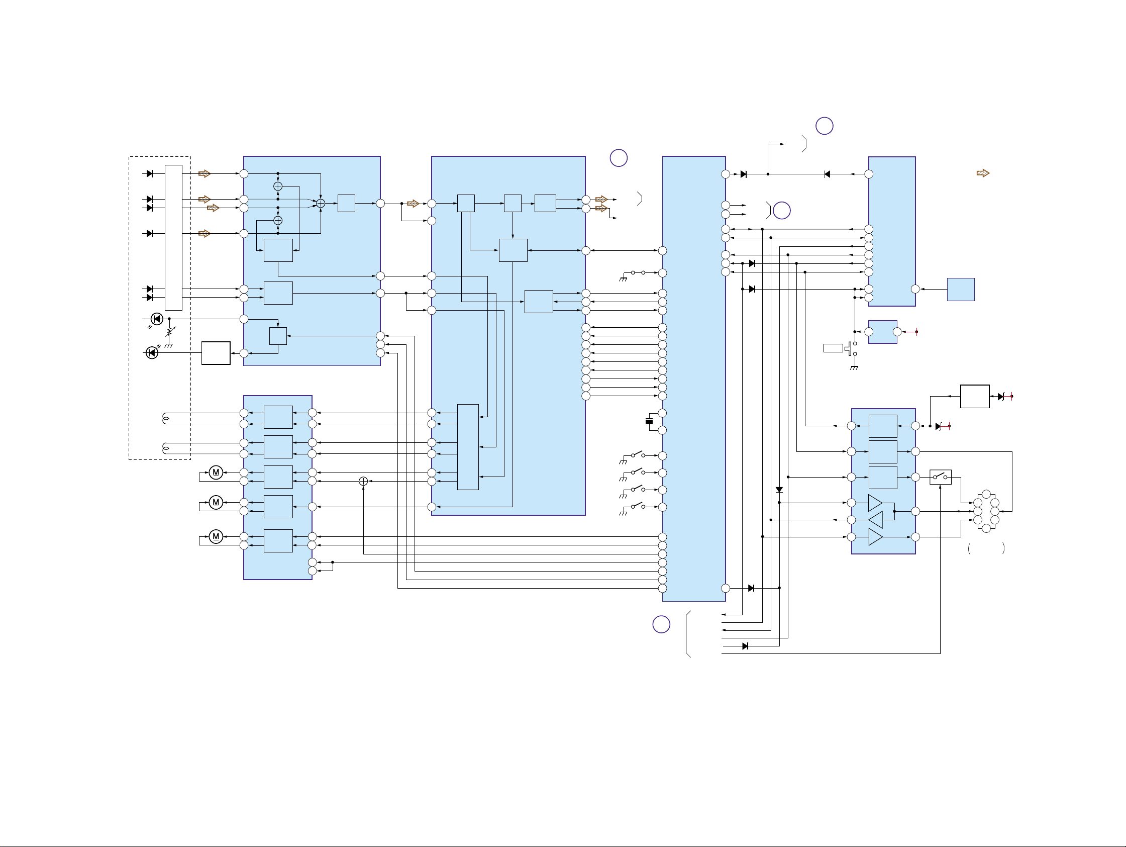
3-2. BLOCK DIAGRAM — CD SECTION —
CDX-CA850/CA850X/CA860X
OPTICAL PICK-UP
KSS-720A
A
C
B
D
PD
LD
TRACKING
E
F
FOCUS
COIL
COIL
CONV.
I-V
M902
SLED
MOTOR
M901
SPINDLE
MOTOR
M903
LOADING
MOTOR
A
5
C
7
B
6
D
8
FOCUS
ERROR
E
11
TRACKING
F
ERROR
10
PD
4
LD
LD
DRIVE
Q101
TRACKING/FOCUS COIL DRIVE
SLED/SPINDLE/LOADING MOTOR DRIVE
10
11
12
13
AMP
LD
3
IC7
FOCUS
COIL
DRIVE
TRACKING
8
COIL
DRIVE
9
SLED
6
MOTOR
7
DRIVE
SPINDLE
MOTOR
DRIVE
LOADING
5
MOTOR
4
DRIVE
RF AMP, LD APC,
ERROR AMP
IC1
22
21
25
24
31
32
18
1
2
MUTE 1
34
MUTE 2
35
RFO RFAC
RF
EQ
FE
TE
LD ON
HOLD SW
AGC CONT
16
14
13
22
21
20
DIGITAL SERVO,
DIGITAL SIGNAL PROCESSOR
IC501
SUB
D/A
CONV.
LOUT1
LOUT2
LOCK
SQSO
SQCK
SCOR
MD2
XRST
DATA
XLAT
SCLK
CLOK
SENS
GFS
FOK
RFDC
FE
TE
SE
FFDR
FRDR
TFDR
TRDR
SFDR
SRDR
MDP
EFM
DEM
SERVO
CTL
61
54
50
52
51
42
43
40
41
38
39
35
D/A
I/F
DIGITAL
CLV
CODE
PROCESS
92
95
34
6
7
24
73
11
13
14
17
15
16
22
32
(Page 24)
TUNER
SECTION
SW3
(LIMIT)
SW1
(DISC IN)
SW4
(DOWN)
SW2
(SELF)
1
CD L
R-CH
(KEY BOARD)
X1
10MHz
CD SYSTEM CONTROL
IC5
BUS CLK
LOCK
46
OPEN
6
SI2
49
SCK2
48
SCOR
64
MD2
71
CD RST
21
CD DATA
67
CD XLAT
68
SCLK
45
CD CKO
65
SENS
57
GFS
55
FOK
54
31
XIN
32
XOUT
SSTP
11
IN SW
62
D SW
10
SELF SW
63
LM EJ
69
LM LOD
66
SLED –
40
DRIVE OE
70
LD ON
20
HOLD
22
AGC CONT
23
A MUT
CDMON
CDON
BUS SI
BUS ON
RESET
BU IN
BUS SO
TUNER
ATT
SECTION
(Page 24)
19
17
MDON
CDON
18
51
52
61
30
60
53
5
DISPLAY
SECTION
(Page 25)
S101
RESET
SYSTEM CONTROL
IC501 (1/3)
ATT
5
UNI CKO
19
UNI SI
17
UNI SO
18
BUS ON
14
SYS RST
22
BU IN
77
SIRCS
RESET
90
HSTX
86
IC502
1 2
RESET
BUS INTERFACE
IC601
BATT (L)
10 3
CHECK
13 2
RESET
BUS ON
12
CONT
9
8
11
DATA
CLK
• Signal path
:CD
Q603
SIRCS
BUFFER
IC903
BATT
BU DET
Q602
6
5
4
CN601
BUS
CONTROL IN
BATT
8
3
2
1
7
24
BU 5V
1
6
4
4
23 23
2
DISPLAY
SECTION
(Page 25)
SRST
BUS CLK
BUS SI
BUS ON
UNI SO
LINK OFF
CDX-CA850/CA850X/CA860X
3-3. BLOCK DIAGRAM — TUNER SECTION —
(ANTENNA)
CN201
TUNER UNIT
TUX201
AM ANT MPX
1 10
2
AMDETFM ANT
RDS DET
S METER
SDA IIC
SCL IIC
SDA EEPROM
SCL EEPROM
• Signal path
:CD
:FM
:AM/MW/LW
1
CD
SECTION
(Page 23)
8
RF AMP
Q204
9 16
14
12
13
17
18
CDL
ADSO(L-CH)
IC304
3 1
CA850
RDS DECODER
IC201
MPX
IC202
NOISE
DET
MPT
DAVN
SCA
SDA
LVIN
10
20
9
72
Q205
ELECTRONIC VOLUME
IC301
4 28
AUXL OUT FL
43
MDL
33
AC INL
38
12
9
16
14
19
20
17
31
50
16
522
758
53
70
71
10
11
ACOUTL
MPX1
AM
QUAL
MP IN
SDA
SCL
SM
VOL ATT
QUALITY
NS MASK
MPTH
DAIN
VSM
I2CSIO
I2CCKO
E2PSIO
E2PCKO
OUT RL
OUTSW
SA CLK
SA OUT
SYSTEM CONTROL
IC501 (2/3)
BEEP
AMP ATT
AMP ON
TEL ATT
ILL IN
ACC IN
XDA
TEST
PW ON
TUN ON
XIA
XO
XI
27
24
21
23
15
30
109
110
117
73
74
108
83
92
93
113
CA850/CA850X
CA860X
3 1
BUFFER
IC308
5 7
CA850/CA850X
4
CD
SECTION
(Page 23)
9
BATT
X501
32.768kHz
X502
3.68MHz
2 13
7 12
SUB WOOFER AMP
IC310
1 4
CA850/CA850X
ATT
POWER
CONT.
Q104(1/2),105
BATT
COM8.5V
BUFFER
IC302
CONTROL
Q303, 304
SA CLK
SA OUT
PWON
ACC
DET
Q101
POWER
Q801-803
POWER
Q201,202
MUTE
CONT
CONT
CA860X
3
DISPLAY
SECTION
(Page 25)
ILL
DET
Q102
COM 8.5V
TU 8V
+5V
REG
Q207
Q103
TU 5V
Q306
Q308
Q310
BATT
CA860X
1 3
POWER AMP
12
11
16
BEEP
22
MUTE
4
STBY
Q104(2/2),106
+10V
REG
IC801
IC351
POWER
CONT.
BATT
R-CH
R-CH
R-CH
5
3
9
7
R-CH
10V
CN302
CN301
CN101
–1
–2
–5
–6
–3
–4
1
9
2
10
4
12
3
11
13
14
7
15
5
6
16
L
R
L
R
L
R
L
R
FL+
FL–
RL+
RL–
FR+
FR–
RR+
RR–
TEL MUTE
ILL
ACC
TEST
AMP REM
ANT REM
BATT
BUS AUDIO IN
AUDIO OUT
FRONT
AUDIO OUT
REAR
SUB OUT
2424
3-4. BLOCK DIAGRAM — DISPLAY SECTION —
CDX-CA850/CA850X/CA860X
2
CD
SECTION
(Page 23)
3
TUNER
SECTION
(Page 24)
LCD901
BUS SI
UNI SO
BUS CLK
BUS ON
LINK OFF
S RST
PW ON
SA CLK
SA OUT
LCD DRIVER
IC901
DATA
CLK
IC702
CE
BUF
100
99
98
SUB SYSTEM CONTROL
UNI SI
98
97
UNI SO
UNI SCK
101
BUS ON
38
LINK OFF
50
RES
76
81
PW ONI
33
SA CLK
1
SA OUT
112
LCD DATA
60
LCD SCK
64
LCD CE1
66
IC701
XTAL
EXTAL
BOOT
ILL ON
SYSTEM CONTROL
IC501 (3/3)
80
79
107
48
46
47
57
82
ADON
KEY ACK
RC IN1
RC IN0
KEY IN0
KEY IN1
BOOT
BOOT
FLASH ON
FLASH ON
85
X701
18.432MHz
86
CA850
J651
(REMOTE IN)
57
52
BATT
POWER
CONT.
Q702,703
LCD+B
KEY
ACTIVE
Q701
KEY IN
MATRIX
LSW921
LCD+B
DIMMER
86
DIMMER
CONTROL
Q903
REG
Q501
LED910-913
LED851
BU5VBATT
S102
(NOSE DET)
LED
DRIVE
Q705,706
58
81
DOOR IND
NOSESW
BATT
POWER
CONT.
Q402,403
+6V REG
Q401
POWER
CONT.
Q405,407
CD 6V
+5V REG
Q406
MD ON
CD ON
CD 5V
5
CD
SECTION
(Page 23)
25 25
 Loading...