Sony CDXC-90-R Service manual
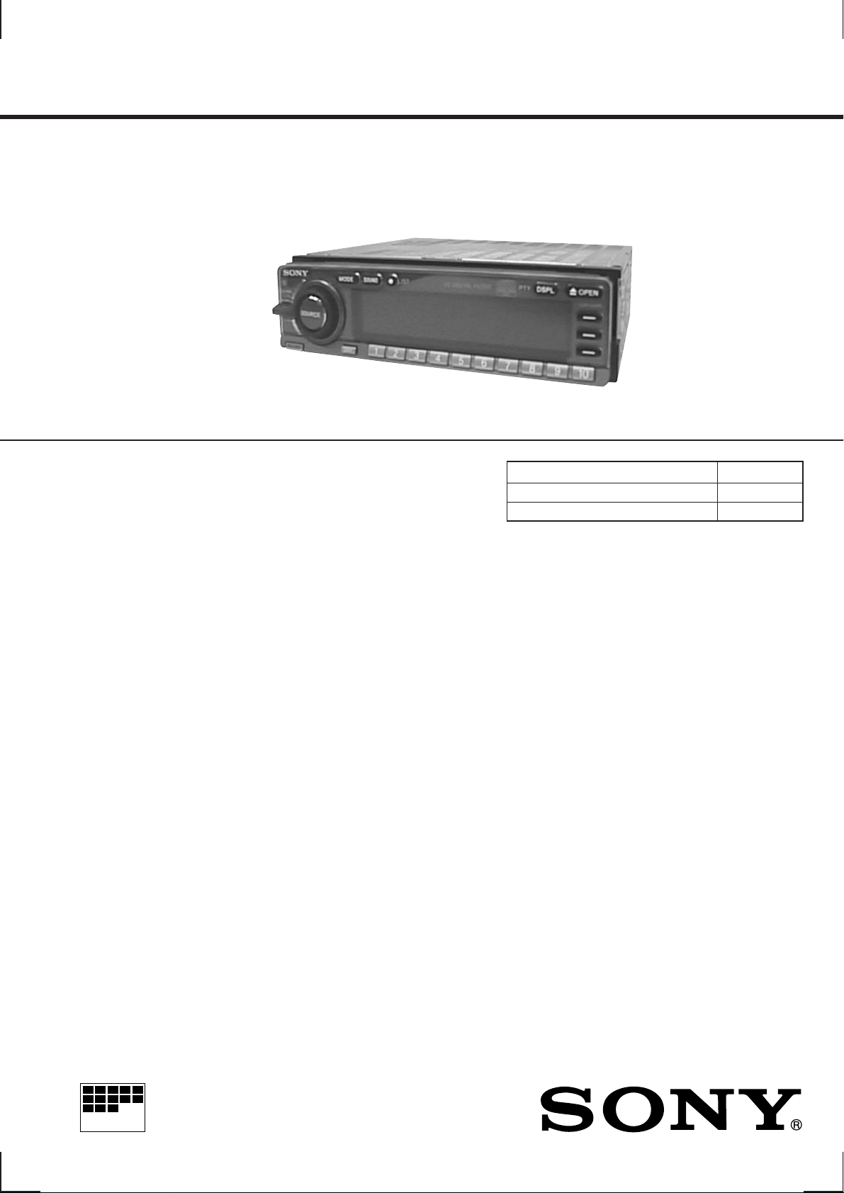
CDX-C90R
SERVICE MANUAL
SPECIFICATIONS
AEP Model
UK Model
Model Name Using Similar Mechanism CDX-C780R
CD Drive Mechanism Type MG-363S-121
Optical Pick-up Name KSS-520A
CD player section
System Compact disc digital audio
system
Signal-to-noise ratio 109 dB
Frequency response 5 - 20,000 Hz (±1 dB)
Wow and flutter Below measurable limit
Laser Diode Properties
Material GaAlAs
Wavelength 780 nm
Emission Duration Continuous
Laser output power Less than 44.6 µW*
* This output is the value measured at a distance of
200 mm from the objective lens surface on the Optical
Pick-up Block.
Tuner section
FM
Tuning range 87.5 - 108.0 MHz
Antenna terminal External antenna connector
Intermediate frequency 10.7 MHz
Usable sensitivity 8 dBf
Selectivity 75 dB at 400 kHz
Signal-to-noise ratio 65 dB (stereo),
68 dB (mono)
Harmonic distortion at 1 kHz
0.3% (stereo),
0.3% (mono)
Separation 35 dB at 1 kHz
Frequency response 20 - 15,000 Hz
MW/LW
Tuning range MW : 531 - 1,602 kHz
LW : 153 - 281 kHz
Antenna terminal External antenna connector
Intermediate frequency 10.71 MHz/450 kHz
Sensitivity MW: 30 dBµV
LW : 33 dBµV
General
Outputs Digital output
Line outputs (3)
Power antenna relay
control lead
Power amplifier control
lead
Telephone ATT control
lead
Illumination control lead
Tone controls Bass ±8 dB at 100 Hz
Treble ±8 dB at 10 kHz
Power requirements 12 V DC car battery
(negative ground)
Dimensions Approx. 178 × 50 × 184 mm
(w/h/d)
Mounting dimension Approx. 182 × 53 × 163 mm
(w/h/d)
Mass Approx. 1.6 kg
Supplied accessories Parts for installation and
connections (1 set)
Rotary remote RM-X90 (1)
Wireless remote RM-X9R (1)
Front panel case (1)
Design and specifications are subject to change without
notice.
FM/MW/LW COMPACT DISC PLAYER
MICROFILM
– 1 –
r
SERVICE NOTE
CAUTION
Use of controls or adjustments or performance of procedures other than those specified herein may result in hazardous radiation exposure.
Notes on Chip Component Replacement
• Never reuse a disconnected chip component.
• Notice that the minus side of a tantalum capacitor may be dam-
aged by heat.
NOTES ON HANDLING THE OPTICAL PICK-UP BLOCK
OR BASE UNIT
The laser diode in the optical pick-up block may suffer electrostatic
breakdown because of the potential difference generated by the
charged electrostatic load, etc. on clothing and the human body.
During repair, pay attention to electrostatic breakdown and also use
the procedure in the printed matter which is included in the repair
parts.
The flexible board is easily damaged and should be handled with
care.
NOTES ON LASER DIODE EMISSION CHECK
The laser beam on this model is concentrated so as to be focused on
the disc reflective surface by the objective lens in the optical pickup block. Therefore, when checking the laser diode emission, observe from more than 30 cm away from the objective lens.
NOTES ON PICK-UP FLEXIBLE BOARD
The pick-up flexible board in this set is secured to the optical pickup with an adhesive tape. Once the tape is removed, an adhering
force becomes weak, and it cannot be reused.
Therefore, if the optical pick-up is replaced, replace also the pickup flexible board with a new one.
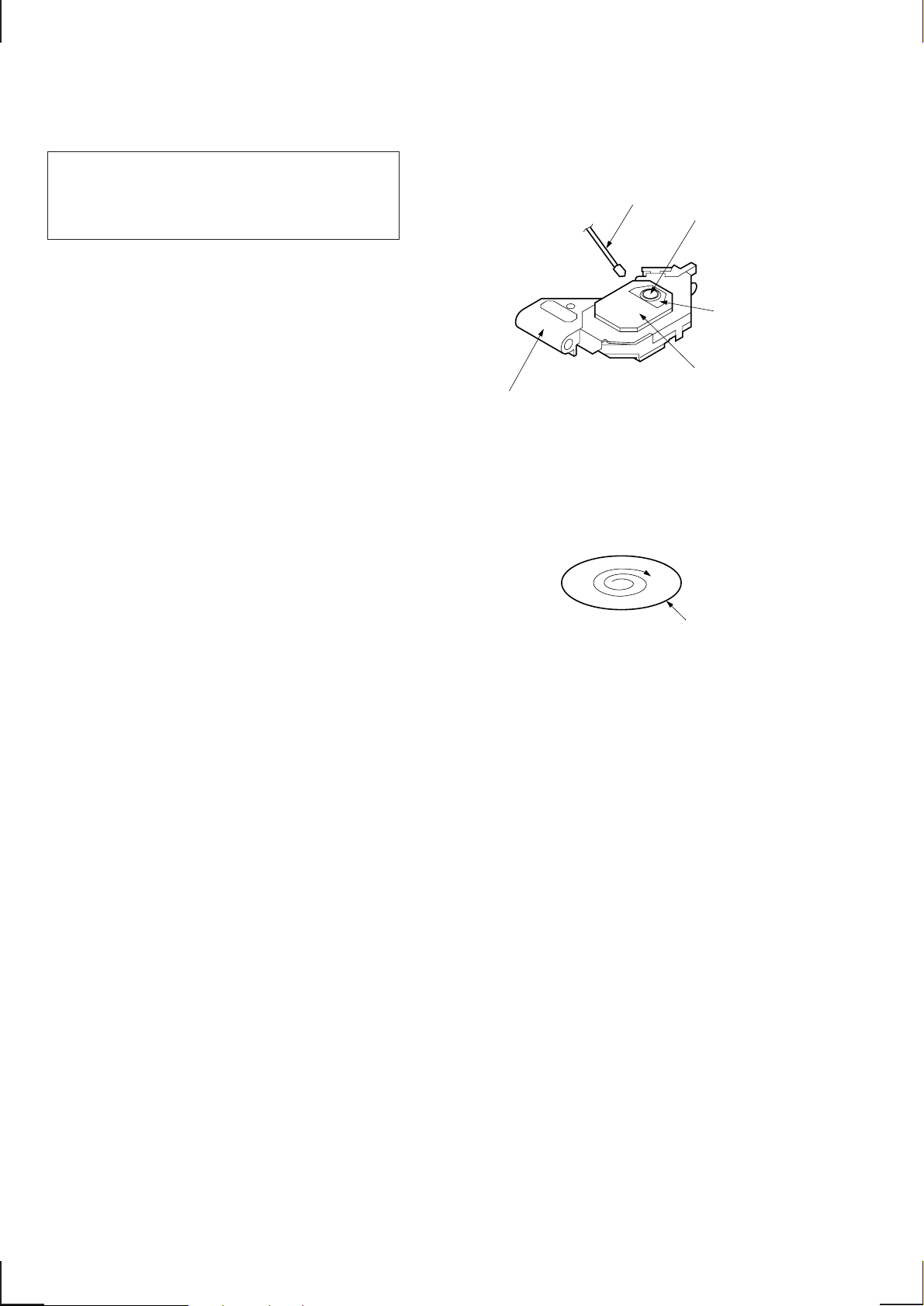
NOTES ON CLEANING THE OBJECTIVE LENS
cotton swabs
optical pick-up
slide base
objective lens
2-axis actuato
2-axis cover
Apply CD lens cleaner B-4 (Part No.:J-2501-000-A) to cotton swabs
(narrow type) (Part No.:J-2501-023-A) to be lightly wet. Use a force
(about 5 g (0.18 oz)) to make the objective lens in contact with the
bottom lightly, and clean the lens by spirals as following below.
Replace the cotton swab and repeat this cleaning two or three times.
surface of objective lens
Notes:
Do not force to push the objective lens. Otherwise, the plate spring
supporting the objective lens will be bent, causing a deteriorated
RF waveform.
Never touch anything other than the objective lens. Otherwise, a
significant deterioration occurs in the RF waveform.
SAFETY-RELATED COMPONENT WARNING!!
COMPONENTS IDENTIFIED BY MARK ! OR DOTTED LINE
WITH MARK ! ON THE SCHEMATIC DIAGRAMS AND IN
THE PARTS LIST ARE CRITICAL TO SAFE OPERATION.
REPLACE THESE COMPONENTS WITH SONY PARTS WHOSE
P ART NUMBERS APPEAR AS SHOWN IN THIS MANU AL OR
IN SUPPLEMENTS PUBLISHED BY SONY.
– 2 –

TABLE OF CONTENTS
1. DISASSEMBLY
1-1. Cover (Upper) .....................................................................4
1-2. Front Panel Assy ................................................................. 4
1-3. Cords ................................................................................... 5
1-4. Rear Panel ........................................................................... 5
1-5. MD Assy .............................................................................6
1-6. Audio Board ........................................................................ 6
1-7. Bracket (MD) ...................................................................... 7
1-8. Motor Block ........................................................................ 7
1-9. Base Panel Assy .................................................................. 8
1-10. Sub Panel Assy.................................................................... 8
1-11. Chassis (Front) Assy ........................................................... 9
1-12. Main Board ......................................................................... 9
1-13. Chassis (T) Sub Assy ........................................................ 10
1-14. Lever Assy ......................................................................... 10
1-15. Servo Board....................................................................... 11
1-16. Roller Assy........................................................................ 11
1-17. Chassis (OP) (O/S) Assy ................................................... 12
1-18. Optical Pick-up Block ....................................................... 12
2. ELECTRICAL ADJUSTMENTS
CD Section ............................................................................ 13
Tuner Section.........................................................................13
3. DIAGRAMS
3-1. IC Pin Descriptions ........................................................... 17
3-2. Block Diagram – CD Section –......................................... 27
3-3. Block Diagram – Main Section –...................................... 29
3-4. Block Diagram – Display Section –.................................. 31
3-5. Circuit Boards Location .................................................... 33
3-6. Printed Wiring Boards – CD Mechanism Section –.......... 33
3-7. Schematic Diagram – CD Mechanism Section (1/3) – ..... 37
3-8. Schematic Diagram – CD Mechanism Section (2/3) – ..... 39
3-9. Schematic Diagram – CD Mechanism Section (3/3) – ..... 41
3-10. Printed Wiring Board – Audio Section –........................... 43
3-11. Schematic Diagram – Audio Section (1/2) –.....................45
3-12. Schematic Diagram – Audio Section (2/2) –..................... 47
3-13. Printed Wiring Boards – Main Section – .......................... 49
3-14. Schematic Diagram – Main Section (1/4) – ...................... 53
3-15. Schematic Diagram – Main Section (2/4) – ...................... 55
3-16. Schematic Diagram – Main Section (3/4) – ...................... 57
3-17. Schematic Diagram – Main Section (4/4) – ...................... 59
3-18. Printed Wiring Board – EL Section –................................ 61
3-19. Schematic Diagram – EL Section – ..................................61
3-20. Printed Wiring Board – Sensor Section – ......................... 62
3-21. Schematic Diagram – Sensor Section – ............................ 62
4. EXPLODED VIEWS
4-1. Case Section ...................................................................... 69
4-2. Front Panel Section ........................................................... 70
4-3. Chassis Section ................................................................. 71
4-4. CD Mechanism Section (1) ............................................... 72
4-5. CD Mechanism Section (2) ............................................... 73
4-6. CD Mechanism Section (3) ............................................... 74
5. ELECTRICAL PARTS LIST.........................................75
– 3 –
SECTION 1
)
DISASSEMBLY
Note : Follow the disassembly procedure in the numerical order given.
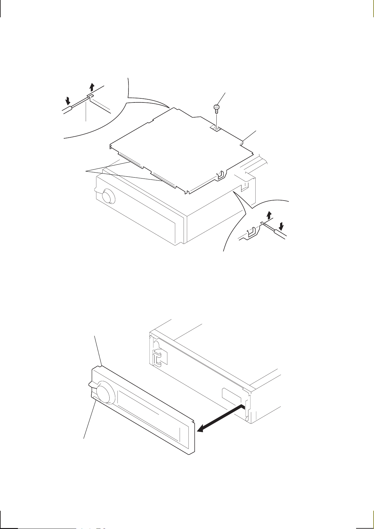
1-1. COVER (UPPER)
5
4
claws
6
1
PTT 2.6x4
7
cover (upper
1-2. FRONT PANEL ASSY
3
front panel assy
3
2
1
Push the button (release).
2
– 4 –
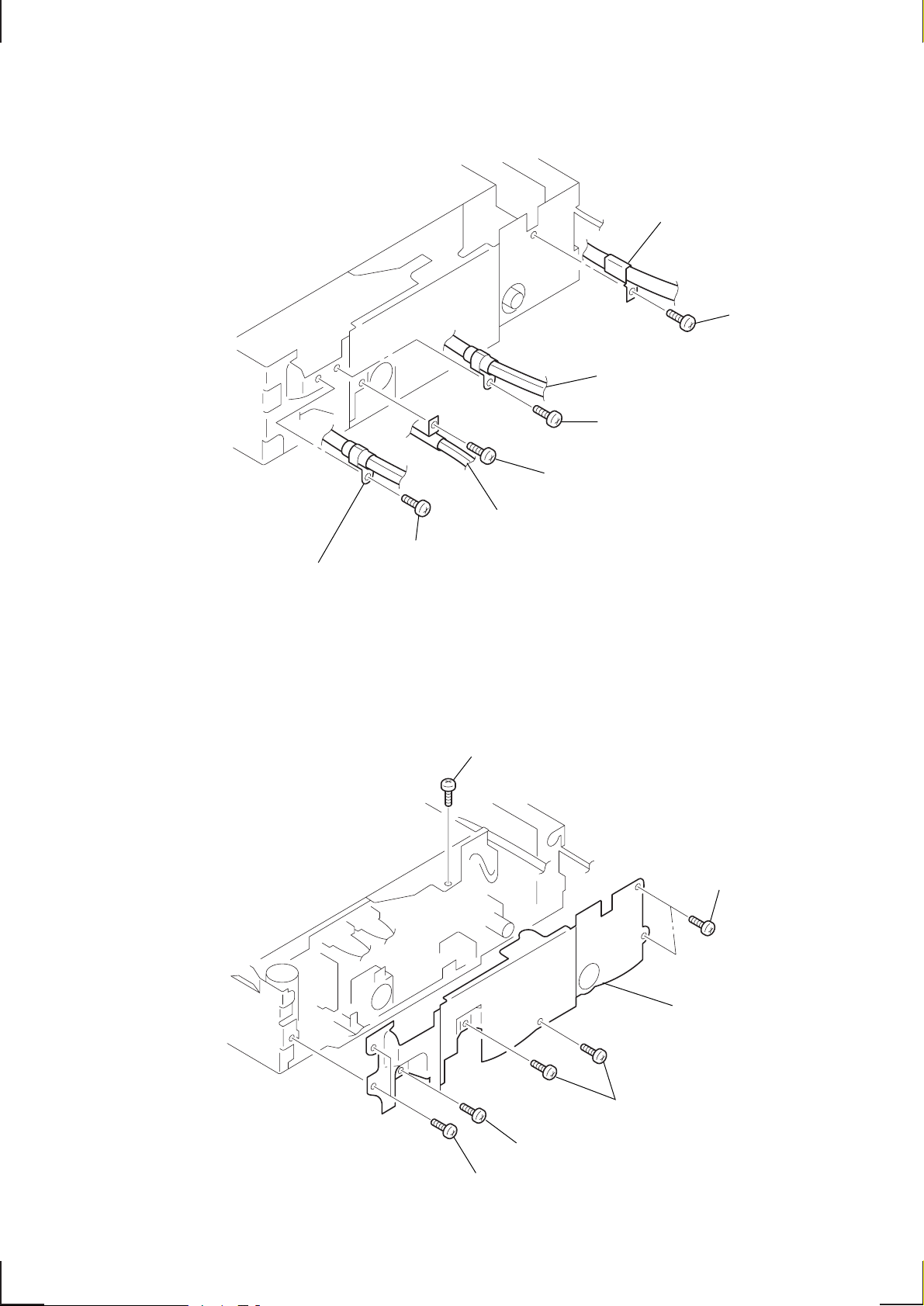
1-3. CORDS
6
1
PTT 2.6x4
2
cord (with connector) (RCA)
(FRONT LINE OUT, REAR LINE OUT)
5
PTT 2.6x4
power cord
8
cord (with connector)
(INVERTER)
(EL transformer unit)
7
4
cord (with connector) (RCA)
(BUS AUDIO IN, SUB OUT)
3
PTT 2.6x4
PTT 2.6x4
1-4. REAR PANEL
5
PTT 2.6x4
1
PTT 2.6x4
6
rear panel
3
PTT 2.6x4
4
PTT 2.6x4
– 5 –
2
PTT 2.6x4
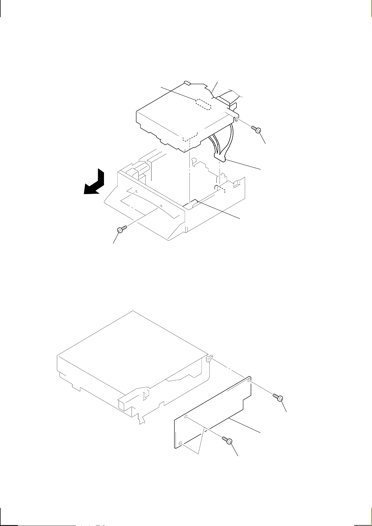
1-5. MD ASSY
4
1
Slide the base panel
in the direction of the
arrow.
5
CN101
7
MD assy
4
CN1
3
PTT 2.6x4
6
CN3
1-6. AUDIO BOARD
2
PTT 2.6x4
2
BVTT 2x
– 6 –
1
BVTT 2x4
3
AUDIO board
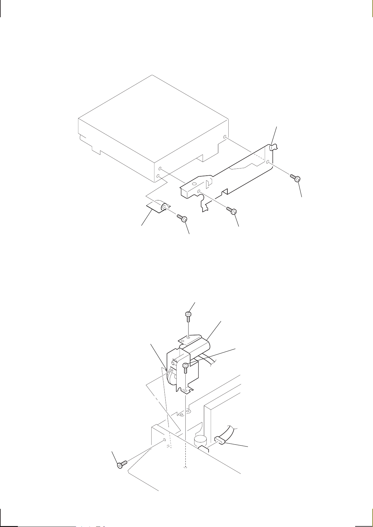
1-7. BRACKET (MD)
5
cover (MD)
4
PTT 2.6x4
1
PTT 2.6x4
3
bracket (MD)
2
PTT 2.6x4
1-8. MOTOR BLOCK
4
P 2X2.5
5
shaft
3
PTT 2.6x4
6
motor block
2
PTT 2.6x4
1
CN600
– 7 –
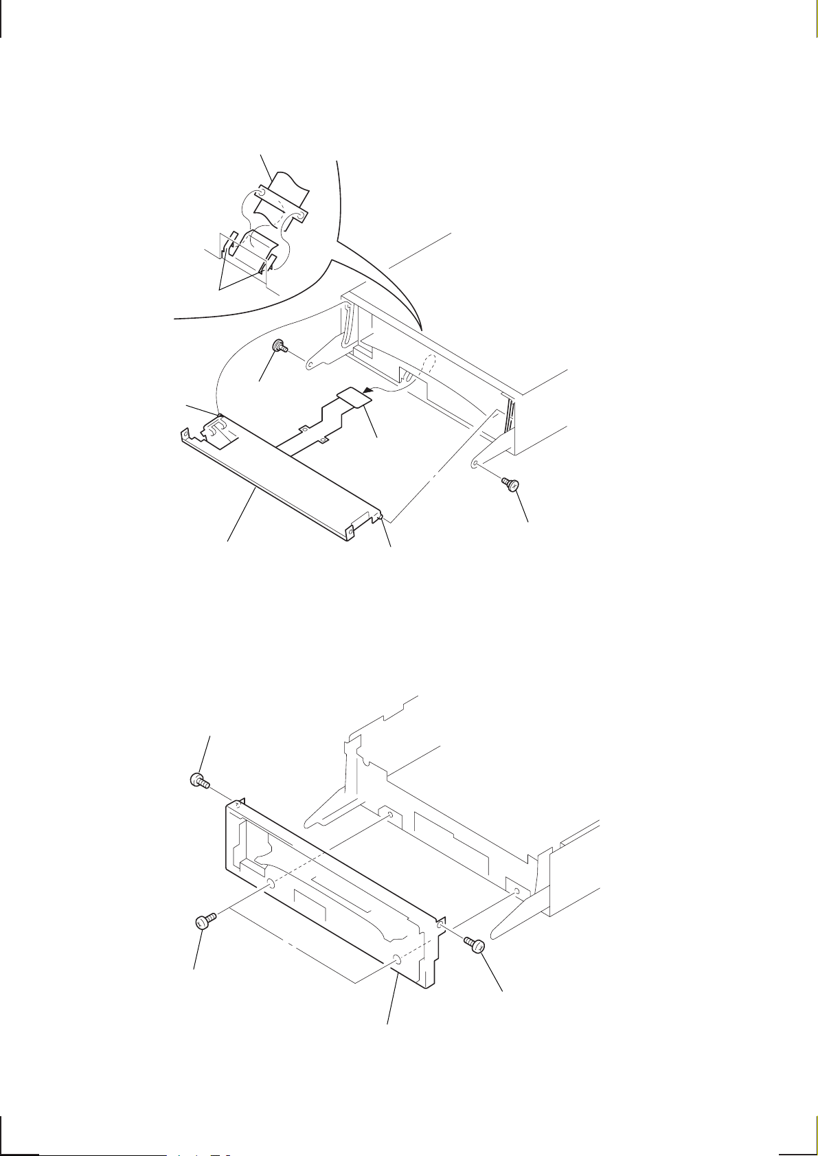
1-9. BASE PANEL ASSY
3
FLEXIBLE board
claws
1
step screw
(M1.7)
5
CN300
1-10. SUB PANEL ASSY
6
base panel assy
1
B 2x4
4
2
step screw (M1.7)
3
PTT 2.6x4
4
sub panel assy
– 8 –
2
B 2x4
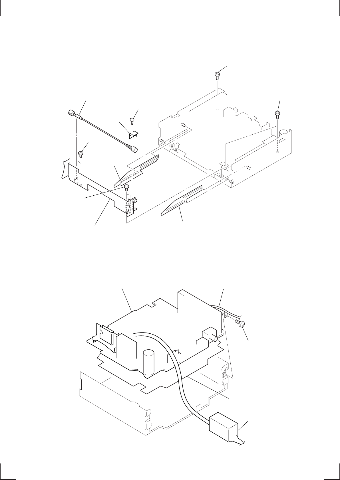
1-11. CHASSIS (FRONT) ASSY
8
shaft (pinion) assy
4
bracket
(shaft pinion)
5
B 2.6x3
9
lever (L) assy
6
B 2.6x3
3
P 2x2.5
1
ground point screw
2
ground point
screws
1-12. MAIN BOARD
7
chassis (front) assy
3
MAIN board
0
lever (R) assy
2
cord (with connector) (ANT)
1
PTT 2.6x4
– 9 –
4
sheet (insulating 90)
power cord
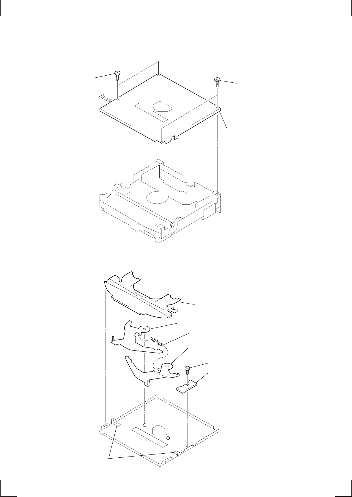
1-13. CHASSIS (T) SUB ASSY
1
P 2x3
2
P 2x3
3
chassis (T) sub assy
1-14. LEVER ASSY
5
6
lever (R) assy
3
tension spring (LR)
7
lever (L) assy
guide (disc)
1
PS 2x4
2
DISC IN SW board
4
claws
– 10 –
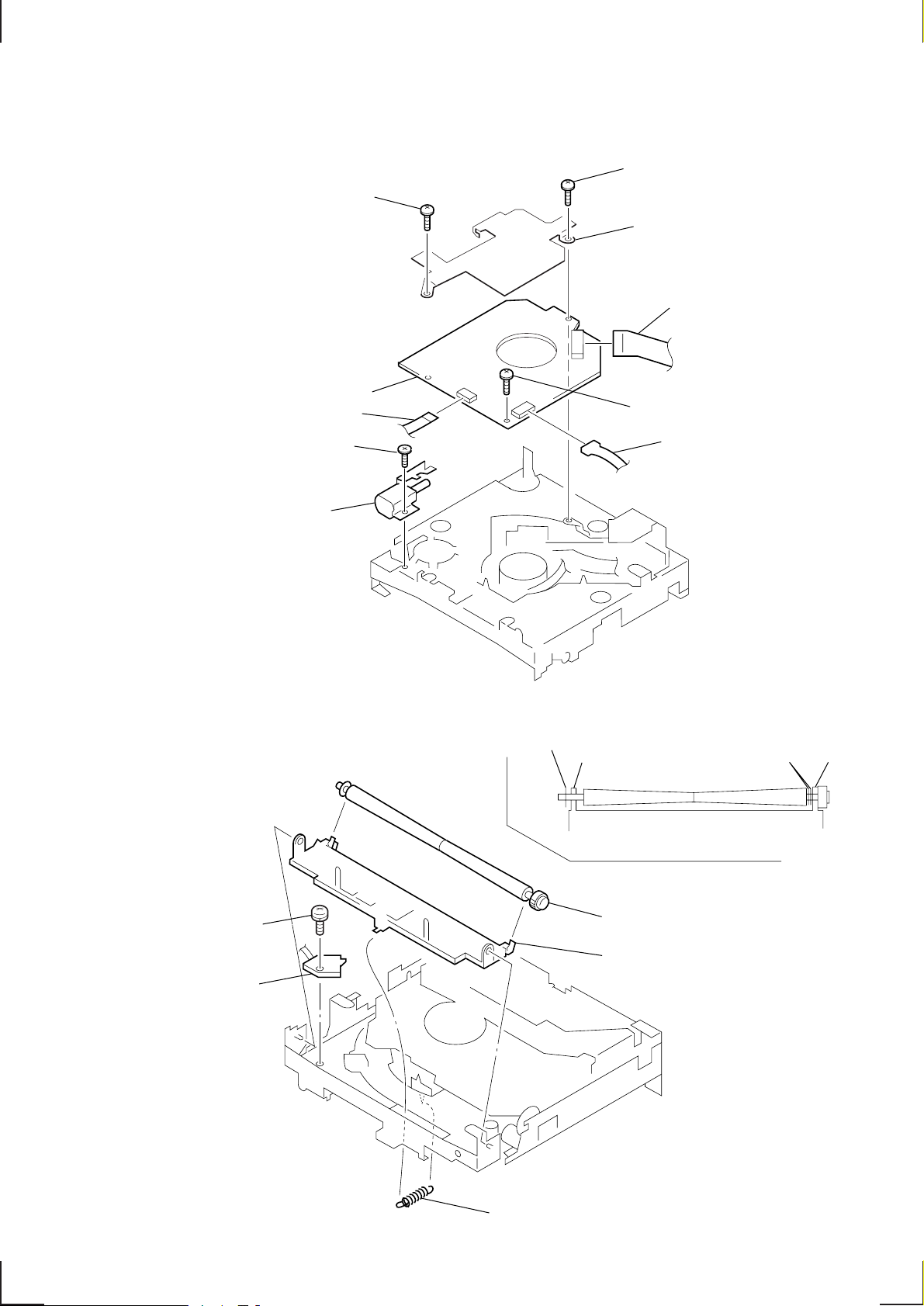
1-15. SERVO BOARD
9
loading motor assy
1
PS 2x5
0
SERVO board
4
8
P 2x3
CN4
2
PS 2x5
3
6
heat sink
7
CN2
PS 2x4
5
CN5
1-16. ROLLER ASSY
• When installing, take note of the positions
arm (roller) and washers. (Fig. 1)
4
PS 2x3
5
LOAD SW board
washer
arm
3
roller assy
2
arm (roller)
arminsulating spacers
Fig. 1
1
tension spring (RA)
– 11 –
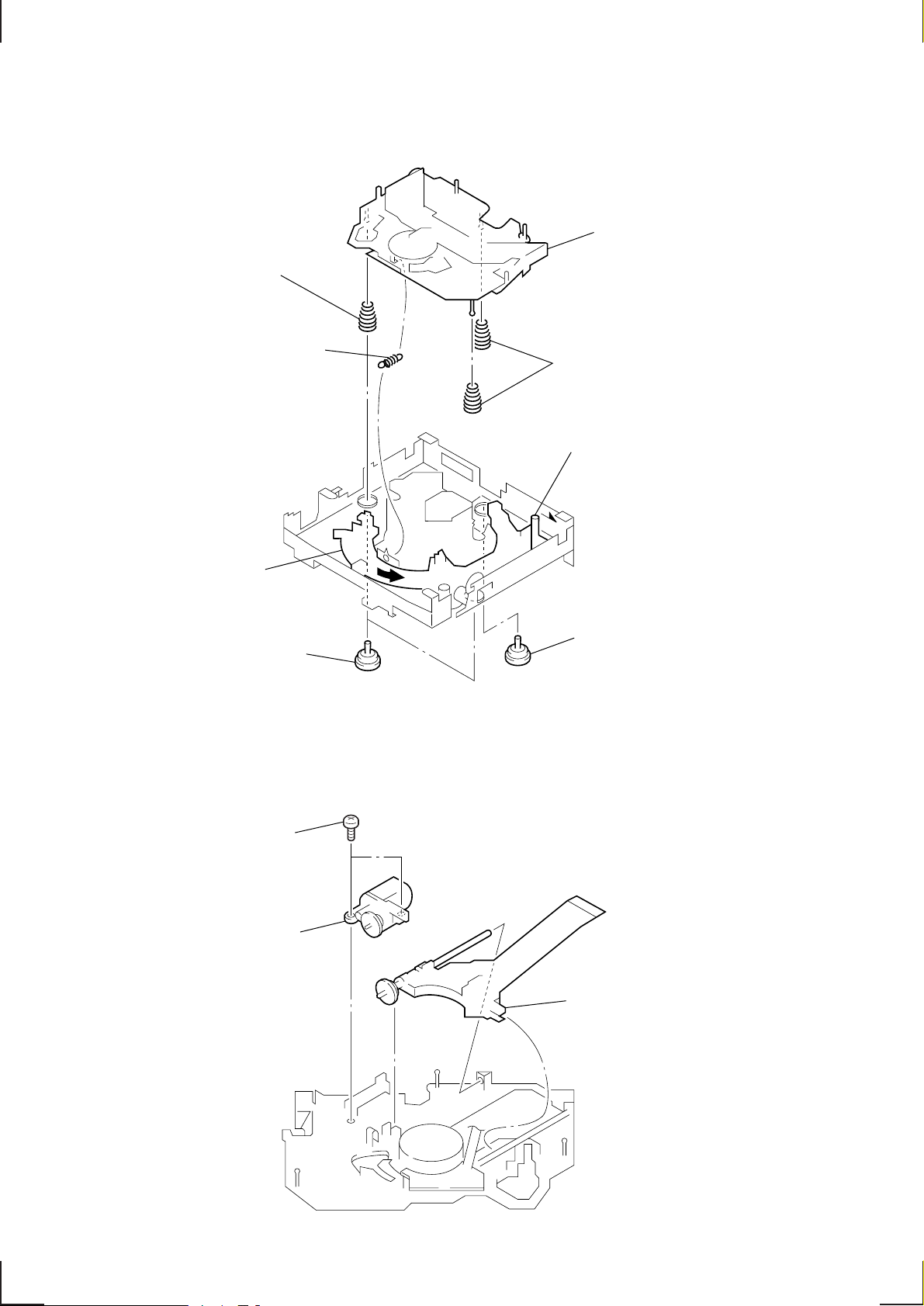
1-17. CHASSIS (OP) (O/S) ASSY
8
compression spring (FL)
1
tension spring (angle)
5
Turn loading ring in the
direction of the arrow.
6
chassis (OP) (O/S) assy
7
compression spring (FL)
4
Fit lever (D) in the
direction of the arrow.
2
damper (T)
1-18. OPTICAL PICK-UP BLOCK
1
P 2x3
2
sled motor assy
3
damper (T)
3
optical pick-up block
– 12 –
SECTION 2
ELECTRICAL ADJUSTMENTS
CD SECTION
CD section adjustments are done automatically in this set.
TUNER SECTION
Cautions during repair
When the tuner unit is defective, replace it by a new one
because its internal block is difficult to repair.
0 dB = 1 µV
TEST MODE
This set have the test mode function. In the test mode, FM Auto
Scan/Stop Level and MW Auto Scan/Stop Level adjustments can
be performed easier than it in ordinary procedure.
<Set the Test Mode>
1. Set the “OFF” mode.
2. Push the preset 4 button.
3. Push the preset 5 button.
4. Press the preset 1 button for more than two seconds.
5. Then the display indicates all lights, the test mode is set.
<Release the Test Mode>
1. Push the OFF button.
Note on Adjustment
The adjustments of tuner section, should be performed according
to the following sequence.
1. FM Auto Scan/Stop Level Adjustment
2. FM Stereo Separation Adjustment (WIDE)
3. FM Stereo Separation Adjustment (NARROW)
4. FM RDS S-Meter Adjustment
5. MW Auto Scan/Stop Level Adjustment
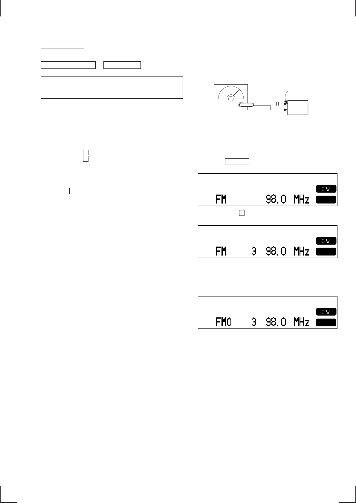
FM Auto Scan/Stop Level Adjustment
Setting :
SOURCE button: FM
FM RF signal
generator
antenna
µ
terminal
F
0.01
Carrier frequency : 98.0 MHz
Output level : 22 dB (12.6 µV)
Mode : mono
Modulation : 1 kHz, 22.5 kHz deviation (30%)
Procedure :
1. Set to the test mode.
2. Push the SOURCE button and set to FM.
Display
3. Push the preset 3 button.
Display
set
D
EL
D
EL
4. Adjust with the volume RV2 on TU701 so that the “FM”
indication turns to “FM0” indication on the display window.
But, in case of already indicated “FM0”, turn the RV2 so that
put out light “0” indication and adjustment.
Display
Adjustment Location : See page 16.
D
EL
– 13 –
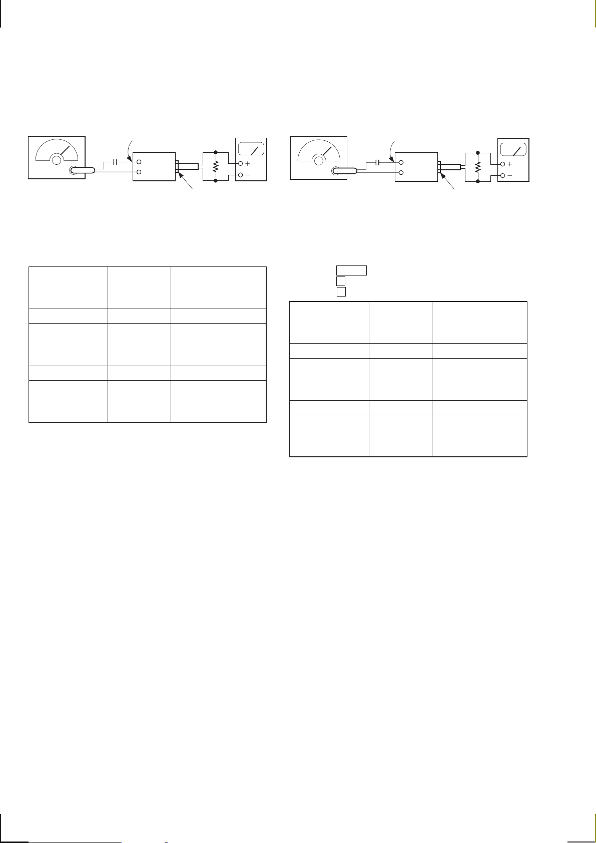
FM Stereo Separation Adjustment (WIDE)
Setting :
SOURCE button : FM
FM Stereo Separation Adjustment (NARROW)
Setting :
SOURCE button : FM
FM RF signal
generator
0.01
Carrier frequency : 98.0 MHz
Output level : 70 dB (3.2 mV)
Mode : stereo
Modulation : main : 1 kHz, 20 kHz deviation (26.5%)
sub : 1 kHz, 20 kHz deviation (26.5%)
19 kHz pilot : 7.5 kHz deviation (10%)
antenna
terminal
µ
F
set
10 k
Ω
LINE OUT REAR
Procedure :
FM stereo
signal generator
output channel
Level meter Level meter
connection reading (dB)
L-CH L-CH A
B
R-CH L-CH Adjust RV3 on TU701
for minimum reading.
R-CH R-CH C
D
L-CH R-CH Adjust RV3 on TU701
for minimum reading.
L-CH stereo separation : A – B
R-CH stereo separation : C – D
The separations of both channels should be equal.
Specification : Separation more than 24 dB
Adjustment Location : See page 16.
level meter
FM RF signal
generator
0.01
Carrier frequency : 98.0 MHz
Output level : 70 dB (3.2 mV)
Mode : stereo
Modulation : main : 1 kHz, 20 kHz deviation (26.5%)
sub : 1 kHz, 20 kHz deviation (26.5%)
19 kHz pilot : 7.5 kHz deviation (10%)
antenna
terminal
µ
F
set
Ω
10 k
LINE OUT REAR
Procedure :
1. Push the SHIFT button.
2. Push the 4 button three times.
3. Push the 5 button twice and set to NARROW mode.
FM stereo
signal generator
output channel
Level meter Level meter
connection reading (dB)
L-CH L-CH A
B
R-CH L-CH Adjust RV4 on TU701
for minimum reading.
R-CH R-CH C
D
L-CH R-CH Adjust RV4 on TU701
for minimum reading.
L-CH stereo separation : A – B
R-CH stereo separation : C – D
The separations of both channels should be equal.
Specification : Separation more than 18 dB
level meter
Adjustment Location : See page 16.
– 14 –
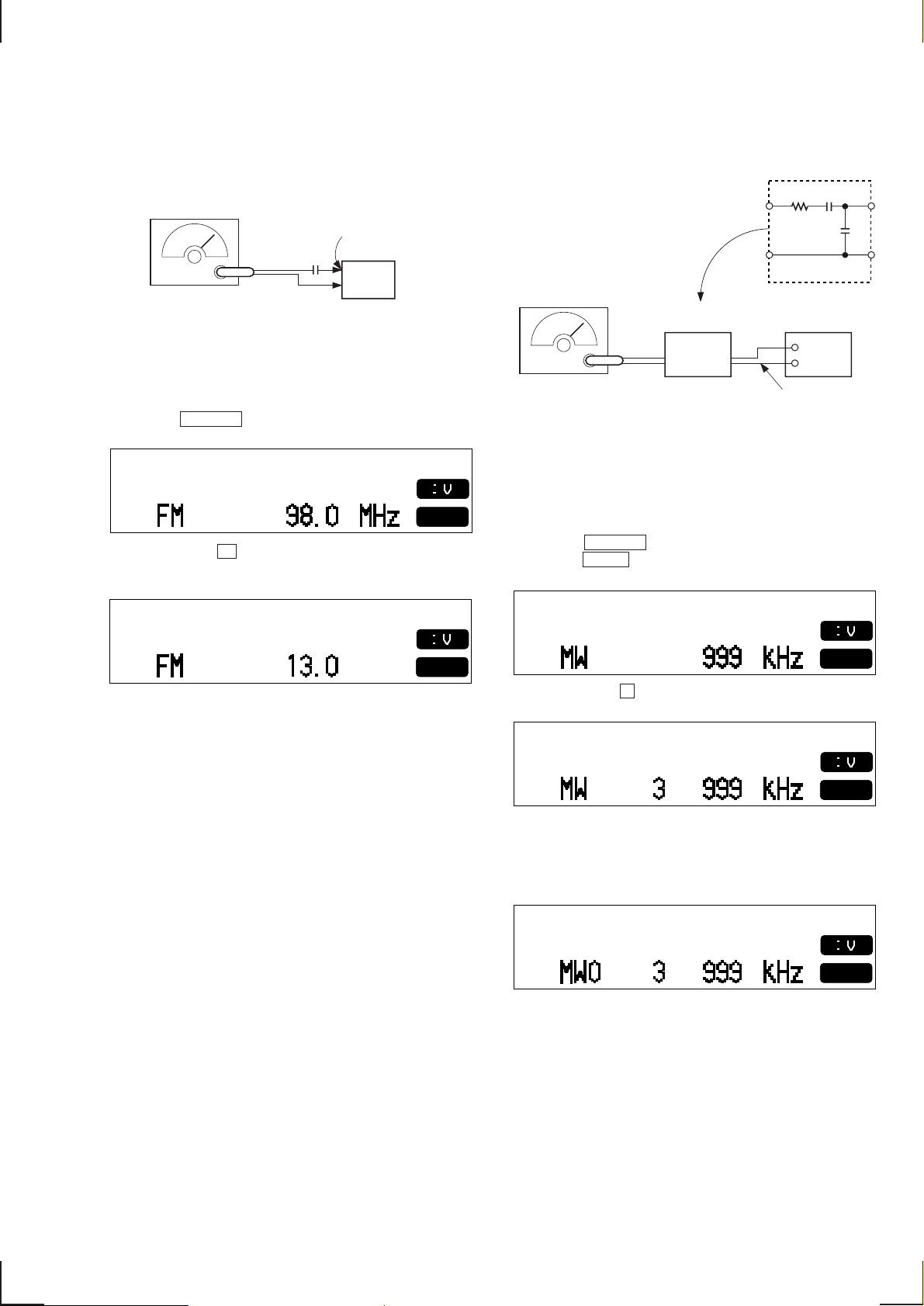
AM RF signal
generator
antenna
terminal
AM dummy
antenna (50
Ω
)
30
Ω
65 pF
15 pF
set
FM RDS S-Meter Adjustment
Setting :
SOURCE button: FM
FM RF signal
generator
antenna
µ
terminal
F
set
0.01
Carrier frequency : 98.0 MHz
Output level : 35 dB (56.2 µV)
Mode : mono
Modulation : no modulation
Procedure :
1. Set to the test mode. (See page 13.)
2. Push the SOURCE button and set to FM.
Display
3. Push the preset 10 button.
4. Adjust RV701 so that the display indication is “13.0”.
Display
D
EL
MW Auto Scan/Stop Level Adjustment
Setting :
SOURCE n MODE button : MW
Carrier frequency : 999 kHz
30% amplitude
modulation by
1 kHz signal
output level : 33 dB (44.7 µV)
Procedure :
1. Set to the test mode. (See page 13.)
2. Push the SOURCE button.
3. Push the MODE button and set to MW .
Display
Specification : Display indication : 12.8 to 13.2.
Adjustment Location : See page 16.
D
EL
D
EL
4. Push the preset 3 button.
Display
D
EL
5. Adjust with the volume RV1 on TU701 so that the “MW”
indication turns to “MW0” indication on the display window.
But, in case of already indicated “MW0”, turn the RV1 so that
put out light “0” indication and adjustment.
Display
D
EL
Adjustment Location : See page 16.
– 15 –
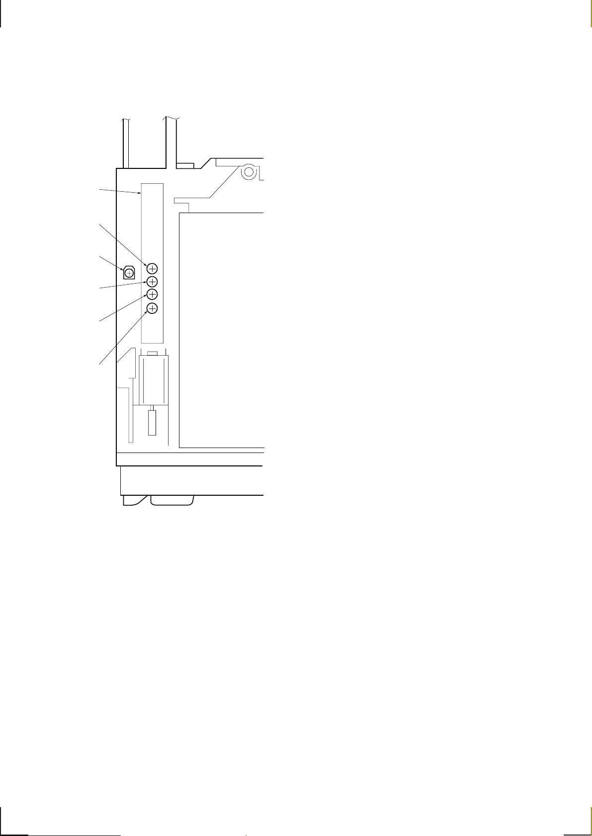
Adjustment Location : tuner unit (TU701)
–set upper view–
TU701
AM AUTO SCAN/
STOP LEVEL ADJ
S-METER ADJ
FM AUTO SCAN/
STOP LEVEL ADJ
FM STEREO
SEPARATION ADJ
FM STEREO
SEPARATION ADJ
RV1
RV701
FM RDS
RV2
RV3
(WIDE)
RV4
(NARROW)
– 16 –
SECTION 3
DIAGRAMS
3-1. IC PIN DESCRIPTIONS
• IC5 CXP84640-011Q (CD SYSTEM CONTROL)
Pin No. Pin Name I/O Pin Description
1 – 5 NCO — Not used in this set.
6 FP OPEN I Front panel open detection input
7 FP CLOSE O Front panel close control output
8 LINKOFF I Bus interface link input (Not used in this set.)
9 DRV OE O Focus/tracking coil/sled motor control output
10 D SW I Down switch input (SW4)
11 – 13 NCO — Not used in this set.
14 LM EJ O Loading motor control output
15 LM LOD O Loading motor control output
16 EMPH O O De-emphasis ON/OFF control output
17 CDMON O CD mechanism deck power control output
18 CD ON O CD power control output
19 A MUT O System attenuate control output
20 LD ON O Laser power ON/OFF control output
21 CD RST O CD system reset output
22 – 24 — — Not used in this set.
25 PH3 I Not used in this set.
26 TSTIN0 I Not used in this set.
27 TSTIN1 I Not used in this set.
28 TST CLV I Not used in this set.
29 NCO — Not used in this set.
30 RESET I System reset input (“L” = Reset)
31 X IN I X’tal oscillator input of system clock. (10 MHz)
32 X OUT O X’tal oscillator output of system clock. (10 MHz)
33 GND — Analog GND
34 XT OUT O Not used in this set.
35 XT IN I Not used in this set.
36 AVSS — A/D converter GND
37 AVREF I A/D converter reference voltage input
38 TEP L I Not used in this set.
39 TEP H I Not used in this set.
40 NCO — Not used in this set.
41 PH2 I Not used in this set.
42 SCLK O CD-TEXT data read clock output
43 ESPXQOK O XQOK signal output to DRAM controller.
44 ESPSDT I Serial data input from DRAM controller.
45 GRSRST O Reset signal output to DRAM controller.
46 GRSCOR I Sub-cord sync input from DRAM controller.
47 CD XLAT O CD signal process serial latch output
48 TX CLK O EEPROM serial clock output
49 TX DATA O EEPROM serial data output
50 UNISO O Not used in this set.
51 BUS CLK I/O Bus system serial clock input/output
52 BUS SI I Bus system serial interface input
53 BUS SO O Bus system serial interface output
54 F OK I Focus OK signal input
55 GFS I GFS signal detection input
56 SCOR O Sub-cord sync output
57 SENS I SENS signal input
58 — I Fixed at “H” in this set.
59 CD CKO O CD signal process serial clock output
– 17 –
Pin No. Pin Name I/O Pin Description
60 BU.IN I Back-up power detection input
61 BUSON I Bus on control input
62 IN SW I Disc in switch input (SW1)
63 SELF SW I Self switch input (SW2)
64 TX CE O EEPROM chip enable output
65 SCK2 O Sub Q read clock output
66 SI2 I Sub Q 80 bit, PCM peak and level data 16 bit input
67 CD DATA O CD signal process serial data output
68 ESPXWRE O Write signal output to DRAM controller.
69 ESPXRDE O Read signal output to DRAM controller.
70 ESPXLT O Serial data latch output to DRAM controller.
71 ESPXSOE O XSOE signal output to DRAM controller.
72 VDD — Power supply
73 HIN I Fixed at “H” in this set.
74 TEXT.ON/OFF I Fixed at “H” in this set.
75 PH1 I Not used in this set.
76 FBTBSEL I Not used in this set.
77 CDOSEL I Not used in this set.
78 – 80 — — Not used in this set.
– 18 –
• IC501 CXD2548R (DIGITAL SERVO, DIGITAL SIGNAL PROCESSOR)
Pin No. Pin Name I/O Pin Description
1 SYSM I System mute input (Not used.)
2 RMUT1 O R-ch, “0” detection output. (“H” : ON, “L” : OFF) (Not used.)
3 LMUT2 O L-ch, “0” detection output. (“H” : ON, “L” : OFF) (Not used.)
4 CKOUT O Master clock frequency division output (Not used.)
5 VDD0 — Digital power supply
6 SBSO O Serial output of sub-P to W.
7 EXCK I Clock input for SBSO read output.
8 SQCK I Clock input for SQSO read output.
9 SQSO O SubQ 80 bit, PCM peak and level data 16 bit output.
10 SENS O SENS output. Output to CPU.
11 SCLK I Clock input for SENS real data read.
12 DATA I Serial data input from CPU.
13 XLAT I Latch input from CPU. Latch serial data at the falling edge.
14 CLOK I Serial data transfer clock input from CPU.
15 XRST I System reset (“L” : Reset)
16 ACDT O Not used.
17 PWM1 I External control input of spindle motor.
18 XLON O Microcomputer extension interface (Output) (Not used.)
19 SPOA I Microcomputer extension interface (Input A) (Not used.)
20 WFCK O WFCK (Write Flame Clock) output
21 GT OP O GTOP output
22 XUGF O XUGF output (Not used.)
23 XPCK O XPLCK output (Not used.)
24 GFS O GFS output
25 RFCK O RFCK output
26 C2PO O C2PO output (Not used.)
27 XROF O XROF output
28 SCOR O “H” output at either detection, sub code sync S0 or S1.
29 MNT0 O MNT0 output (Not used.)
30 MNT1 O MNT1 output (Not used.)
31 MNT3 O MNT3 output (Not used.)
32 VSS1 — Digital GND
33 DOUT O Digital-Out output
34 ATSK I For anti-shock.
35 MIRR O Mirror signal output (Not used.)
36 DFCT O Diffect signal output (Not used.)
37 FOK O Focus OK signal output
38 VDD1 — Digital power supply
39 VPCO1 O Charge pump output for wideband EFM PLL.
40 VPCO2 O VCO2 charge pump output for wideband EFM PLL.
41 VCK.I I VCO2 oscillator input for wideband EFM PLL.
42 V16M O VCO2 oscillator output for wideband EFM PLL.
43 VCTL I VCO2 control input for wideband EFM PLL.
44 PCO O Charge pump output for master PLL.
45 FILO O Filter output for master PLL (Slave = digital PLL).
46 FILI I Filter input for master PLL.
47 AVSS4 — Analog GND
48 CLTV I VCO control voltage input for master.
49 AVDD4 — Analog power supply
50 RFAC I EFM signal input
51 BIAS I Asymmetry circuit constant current input
52 ASY.I I Asymmetry comparate voltage input
– 19 –
Pin No. Pin Name I/O Pin Description
53 ASY.O O EFM full-swing output (“L” : VSS, “H” : VDD)
54 VC I Center voltage input
55 FE I Focus error signal input
56 SE I Sled error signal input
57 TE I Tracking error signal input
58 CE I Center error signal input
59 RFDC I RF signal input
60 RFC I Condenser connection pin for LPF time constant of RF signal.
61 ADIO O OP amplifier output (Not used.)
62 AVSS3 — Analog GND
63 IGEN I Current source reference resistor connection for OP amplifier.
64 AVDD3 — Analog power supply
65, 66 TES2, 3 I TEST pin (Fixed at “L”.)
67 VSS2 — Digital GND
68 TEST I TEST pin (Fixed at “L”.)
69 SFDR O Sled drive output
70 SRDR O Sled drive output
71 TFDR O Tracking drive output
72 TRDR O Tracking drive output
73 FFDR O Focus drive output
74 FRDR O Focus drive output
75 VDD2 — Digital power supply
76 COUT O Track number count signal output (Not used.)
77 LOCK O Not used.
78 MDS O Servo control output of spindle motor. (Not used.)
79 MDP O Servo control output of spindle motor.
80 SSTP I Disc most inner track detection signal input
81 FSTO O 2/3 frequency division output of pins 103 and 104.
82 FSTI I Reference clock input for digital servo.
83 XTSL I X’tal select input (“L” : 16.9344 MHz)
84 C4M O 4.2336 MHz output
85 WDCK O D/A interface. Word clock f = 2Fs
86 VDD3 — Digital power supply
87 LRCK O D/A interface. LR clock f = Fs
88 LRCKI I LR clock input to DAC. (48 bit slot) (Not used.)
89 PCMD O D/A interface. Serial data (2’s COMP, MSB first)
90 PCMDI I Audio data input to DAC. (48 bit slot) (Not used.)
91 BCK O D/A interface. Bit clock
92 BCKI I Bit clock input to DAC. (48 bit slot) (Not used.)
93 EMPH O Not used.
94 EMPHI I De-emphasis ON/OFF of DAC. (“H” : ON, “L” : OFF) (Not used.)
95 VSS3 — Digital GND
96 A VSS1 — L-ch, Analog GND.
97 AVDD1 — L-ch, Analog power supply.
98 AOUT1 O L-ch, Analog output. (Not used.)
99 AIN1 I L-ch, OP amplifier input. (Not used.)
100 LOUT1 O L-ch, LINE output. (Not used.)
101 AVSS1 — L-ch, Analog GND.
102 XVDD — Analog power supply for master clock.
103 XTAI I X’tal oscillator input of master clock (16.9344 MHz).
104 XTAO O X’tal oscillator output of master clock. (Not used.)
105 XVSS — Analog GND for master clock.
106 AVSS2 — R-ch, Analog GND.
– 20 –
Pin No. Pin Name I/O Pin Description
107 ROUT2 O R-ch, LINE output. (Not used.)
108 AIN2 I R-ch, OP amplifier input. (Not used.)
109 AOUT2 O R-ch, Analog output. (Not used.)
110 AVDD2 — R-ch, Analog power supply.
111 A VSS2 — R-ch, Analog GND.
112 VSS0 — Digital GND
– 21 –
• IC300 MB90F574PFV-G-140-BND (SYSTEM CONTROL)
Pin No. Pin Name I/O Pin Description
1 TIR WR O TIR IC data write output
2 TIR RD O TIR IC data read output
3 TIR CE O TIR IC data chip enable output
4 TIR CE O XTIR IC data chip enable output
5 TIR BUSY I TIR IC busy input
6 TIR PDOWN O TIR IC power down output
7 DIVER O FM diversity ON/OFF output (Not used in this set.)
8 VCC — Power supply pin (+5 V)
9 AF SEEK O AF SEEK output
10 WIDE O WIDE/NARROW select output
11 CAUTION I Caution alarm setting (Fixed at “H” in this set.)
12 NOSE SW I Nose detection input
13 COLOR O Color control output (“H”:green, “L”:amber)
14 BUSON O Bus ON control output
15 BEEP O BEEP output
16 TIR RES O TIR IC reset (Power down) output
17 DF LAT O Digital filter latch output
18 DF SO O Digital filter serial data output
19 DF CKO O Digital filter clock output
20 UNISI I Serial data input (for SONY BUS)
21 UNISO O Serial data output (for SONY BUS)
22 UNICK O Serial clock output (for SONY BUS)
23 NCO — Not used.
24 SIRCS I Remote commander input
25 PLLSI I PLL data input
26 PLLSO O PLL data output
27 PLLCKO O PLL clock output
28 PLL CE O PLL chip enable output
29 P MOT+ O Front panel motor control (+) output
30 P MOT– O Front panel motor control (–) output
31 I DET I Panel motor lock detection input
32 POS0 I Position detection input 0 (Open end)
33 GND — GND
34 C — Power stabilization capacitor pin
35 POS1 I Position detection input 1 (Close end)
36 POS2 I Position detection input 2 (10 DEG.)
37 POS3 I Position detection input 3 (20 DEG.)
38 DVCC — D/A converter VREF input
39 DVSS — GND of D/A converter.
40 MOTREF O Motor reference voltage output
41 LCDANG O LCD view angle adjustment analog output
42 AVCC — Analog power supply pin (+5 V)
43 AVRH — A/D converter VREF+ input
44 AVRL — A/D converter VREF– input
45 AVSS — Analog GND
46 DSTSEL0 I Destination select input 0 (Fixed at “H” in this set.)
47 H TEMP I High templature detection analog input (Fixed at “H” in this set.)
48 L TEMP I Low templature detection analog input (Fixed at “H” in this set.)
49 MPT I Tuner multi-pass input
50 VSM I S-Meter voltage detection input
51 RC IN0 I Rotary commander input 0
52, 53 KEYIN0, 1 I Key input 0, 1
– 22 –
 Loading...