

Sony CDX-C8050X Service Manual
CDX-C8050X
SERVICE MANUAL
SUPPLEMENT-2
File this supplement with the service manual.
Subject : Correction
Change of Circuit Boards.
(ECN-CSA02398, CSA02816, CSA02817)
US Model
TABLE OF CONTENTS
1. CORRECTION ...................................................................2
2. CHANGE OF CIRCUIT BOARDS
2-1. Discrimination..................................................................... 4
2-2. Printed Wiring Board –Main Section– ................................ 6
2-3. Schematic Diagram –Main Section (1/4)– .......................... 8
2-4. Schematic Diagram –Main Section (2/4)– .......................... 9
2-5. Schematic Diagram –Main Section (3/4)– ........................ 10
2-6. Schematic Diagram –Main Section (4/4)– ........................ 11
2-7. Printed Wiring Board –DSO Section– .............................. 12
2-8. Schematic Diagram –DSO Section– ................................. 13
2-9. Printed Wiring Board –Sub (CD) Section– ....................... 14
2-10. Schematic Diagram –Sub (CD) Section–.......................... 15
2-11. Printed Wiring Board –Key Section–................................ 16
2-12. Schematic Diagram –Key Section–...................................17
2-13. Electrical Parts List ........................................................... 18
1

1. CORRECTION
! : indicates corrected portion.
Page 48.
INCORRECT CORRECT
24
22
23
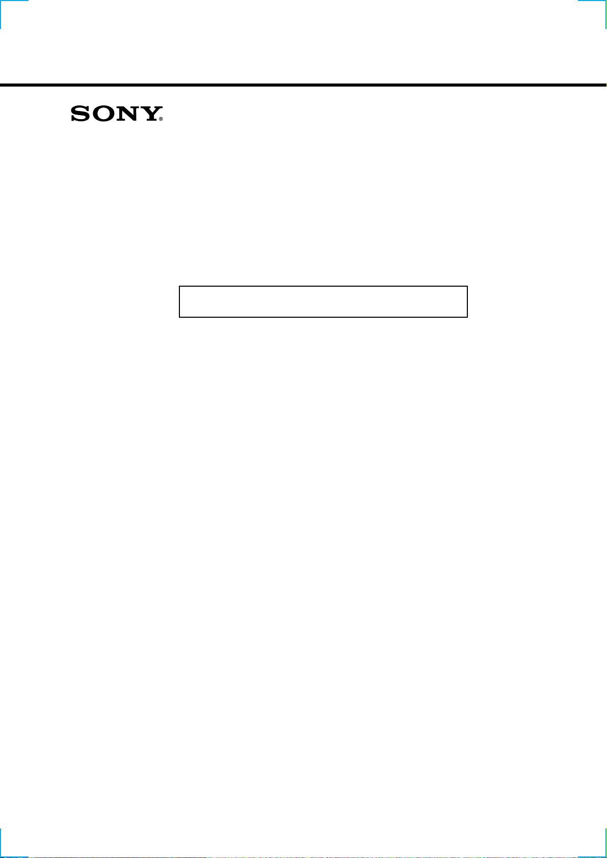
Ref. No. Part No. Description Remark
18 1-792-602-11 CORD (WITH CONNECTOR) (SUB OUT)
21 3-035-250-02 SCREW (LOCK)
12
11
15
^
24
22
23
12
11
15
%
25
Ref. No. Part No. Description Remark
18 1-790-355-52 CORD (WITH CONNECTOR) (RCA) (SUB OUT)
$$
21 3-047-812-01 SCREW (LOCK)
$
* 25 3-049-439-02 SHEET (IC), RADIATION
$
Page 49.
INCORRECT CORRECT
#6
#6
54
Ref. No. Part No. Description Remark
* 66 3-041-371-02 SHEET (REFLECTOR)
#6
#6
5467
#
Ref. No. Part No. Description Remark
* 66 3-041-371-11 SHEET (REFLECTOR)
$
67 3-045-596-01 CUSHION (OFF)
$
2
Page 50.
INCORRECT CORRECT
C
104
M903
107
#7
Ref. No. Part No. Description Remark
#7
#8
Page 64.
INCORRECT CORRECT
C
104
M903
111
#
107
#7
112
#8
#7
Ref. No. Part No. Description Remark
* 111 3-045-857-01 HEAT SINK (CD)
#
$
112 3-046-626-01 SHEET, RADITION
$
Ref. No. Part No. Description Remark
18 1-792-602-11 CORD (WITH CONNECTOR) (SUB OUT)
Ref. No. Part No. Description Remark
18 1-790-355-52 CORD (WITH CONNECTOR) (RCA) (SUB OUT)
$$
3
2. CHANGE OF CIRCUIT BOARDS
When performing service and inspection, check the part number of
the main, DSO, sub (CD) and key boards.
2-1. DISCRIMINATION
MAIN BOARD (SIDE A)
DSO BOARD (SIDE A)
DSO board part No.
Former : 1-677-864-11
New : 1-677-864-12
Main board part No.
Former : 1-677-862-11
New : 1-677-862-12
SUB(CD) BOARD (SIDE A)
Sub(CD) board part No.
Former : 1-677-863-11
New : 1-677-863-12
KEY BOARD (SIDE A)
Key board part No.
Former : 1-677-058-12
New : 1-677-058-13
4
THIS NOTE IS COMMON FOR PRINTED WIRING
BOARDS AND SCHEMATIC DIAGRAMS.
(In addition to this, the necessary note is
printed in each block.)
( ) : Refer to page of supplement-2.
< > : Refer to page of service manual.
for schematic diagram:
• All capacitors are in µF unless otherwise noted. pF: µµF
50 WV or less are not indicated except for electrolytics
and tantalums.
• All resistors are in Ω and 1/
specified.
4
W or less unless otherwise
• % : indicates tolerance.
f
•
: internal component.
• C : panel designation.
• U : B+ Line.
• Power voltage is dc 14.4V and fed with regulated dc power
supply from ACC and BATT cords.
• Voltages are tak en with a V OM (Input impedance 10 MΩ).
Voltage variations may be noted due to normal production tolerances.
• Wavefor ms are taken with a oscilloscope.
Voltage variations may be noted due to normal production tolerances.
• Circled numbers refer to waveforms.
• Signal path.
F : FM
f : AM
J : CD
for printed wiring boards:
• X : parts extracted from the component side.
• Y : parts extracted from the conductor side.
a
•
: Through hole.
• b : Pattern from the side which enables seeing.
(The other layer’s patterns are not indicated.)
Caution:
Pattern face side: Parts on the pattern face side seen from the
(Side B) pattern face are indicated.
Parts face side: Parts on the parts face side seen from the
(Side A) parts face are indicated.
55

CDX-C8050X
• Semiconductor Location (Side A)
Ref. No. Location
D101 I-4
D102 I-4
D104 H-5
D105 F-8
D106 B-2
D107 B-1
D108 K-3
D109 J-3
D201 G-12
D202 D-13
D205 F-12
D301 C-6
D302 D-7
D352 C-8
D353 C-7
D354 C-8
D401 H-5
D601 G-7
D602 H-7
D603 F-8
D607 F-7
D608 G-7
D609 F-7
D610 G-7
D614 G-8
D701 J-12
D702 H-11
D703 I-13
D751 K-12
D752 J-12
D753 K-13
D754 K-11
D755 K-11
D756 J-12
D757 J-12
D758 K-13
D759 K-13
D760 J-13
D761 K-11
D762 J-13
IC301 G-10
IC302 I-3
IC303 D-9
IC304 D-11
IC305 D-10
IC502 I-7
IC503 J-5
IC504 J-5
IC601 G-7
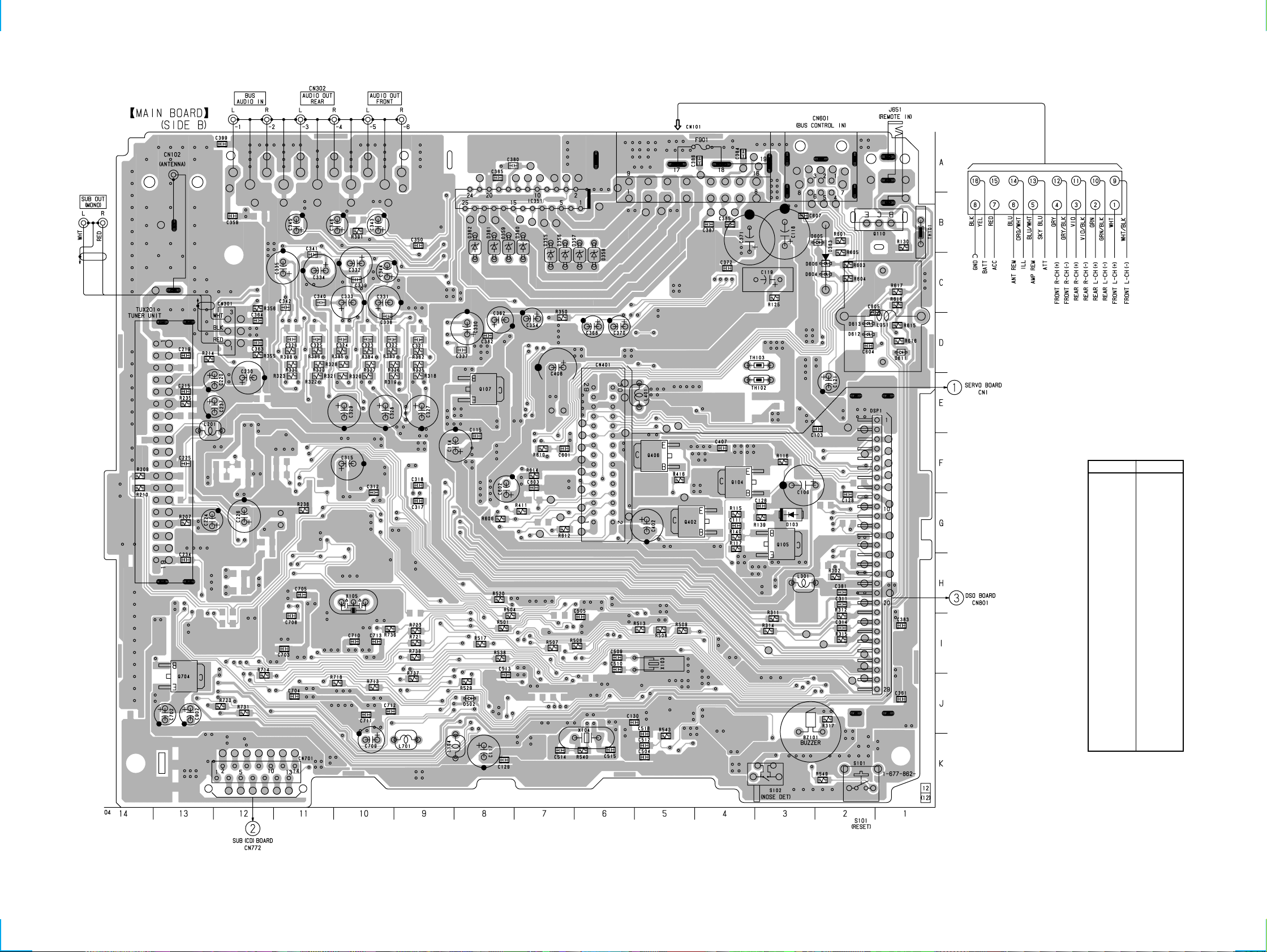
2-2. PRINTED WIRING BOARD — MAIN SECTION —
Ref. No. Location
IC701 J-10
IC702 H-11
Q101 I-4
Q102 H-4
Q103 H-4
Q106 H-4
Q108 E-8
Q109 E-8
Q111 K-7
Q112 J-4
Q113 K-4
Q201 F-13
Q202 E-13
Q203 E-12
Q204 E-12
Q205 E-13
Q206 D-13
Q207 D-13
Q209 F-13
Q351 K-3
Q352 C-8
Q353 C-7
Q354 C-6
Q355 C-7
Q356 B-10
Q357 B-10
Q358 B-11
Q359 B-11
Q360 C-12
Q361 D-12
Q363 C-5
Q364 C-5
Q365 D-5
Q366 D-4
Q403 H-6
Q407 F-5
Q601 G-7
Q602 H-7
Q603 F-7
Q604 F-8
Q605 D-2
Q701 J-12
Q702 J-13
Q703 I-13
Q705 H-13
Q901 I-13
Q902 J-13
Q903 J-13
66
CDX-C8050X
<Page 31>
(Page 12)
• Semiconductor
Location (Side B)
Ref. No. Location
D103 G-3
D355 B-7
D356 B-7
D357 B-7
D358 B-6
D359 B-8
D360 B-7
D361 B-8
D362 B-8
D363 B-2
D502 J-8
D604 C-2
D605 B-2
D606 C-2
D611 D-1
D612 D-2
D613 D-2
IC351 B-7
Q104 F-4
Q105 G-3
Q107 E-8
Q110 B-1
Q402 G-5
Q406 F-5
Q704 J-13
(Page 14)
77
CDX-C8050X
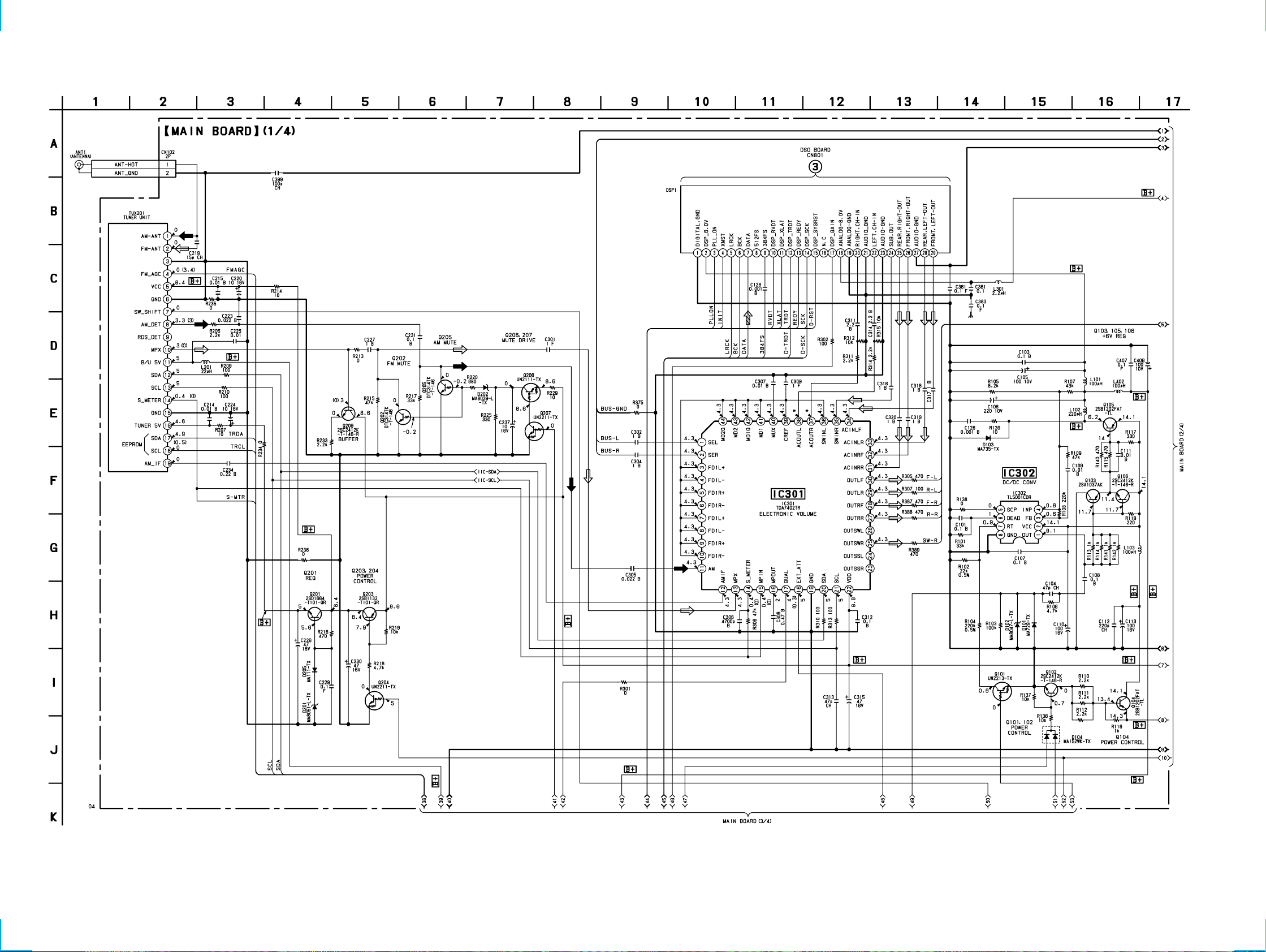
2-3. SCHEMATIC DIAGRAM — MAIN SECTION (1/4) — • Refer to page 46 of Service manual for IC Block Diagrams.
(Page 13)
(Page 9)
(Page 10)
Note:
• Voltage is dc with respect to ground under no-signal
(detuned) condition.
no mark : FM
(): AM
: Impossible to measure
∗
88
 Loading...