

Page 1
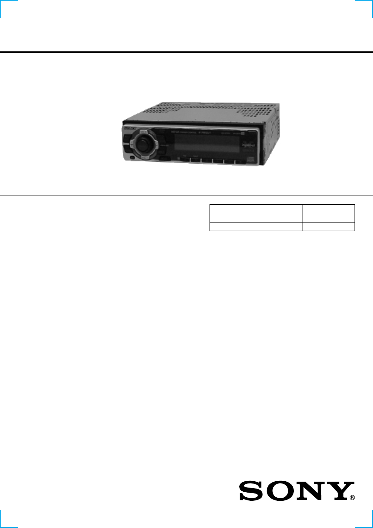
CDX-C7000X/C7050X
SERVICE MANUAL
Photo: CDX-C7050X
• The tuner and CD sections have no adjustments.
SPECIFICATIONS
AUDIO POWER SPECIFICATIONS
POWER OUTPUT AND TOTAL HARMONIC DISTORTION
19 watts per channel minimum continuous average power into
4 ohms, 4 channels driven from 20 Hz to 20 kHz with no more
than 1% total harmonic distortion.
Other Specifications
CD player section
System Compact disc digital audio
Signal-to-noise ratio 90 dB
Frequency response 10 – 20,000 Hz
Wow and flutter Below measurable limit
Laser Diode Properties
Material GaAlAs
Wavelength 780 nm
Emission Duration Continuous
Laser output power Less than 44.6 µW*
* This output is the value measured at a distance
of 200 mm from the objective lens surface on the
Optical Pick-up Block.
Tuner section
FM
Tuning range 87.5 – 107.9 MHz
Antenna terminal External antenna connector
Intermediate frequency 10.7 MHz/450 kHz
Usable sensitivity 8 dBf
Selectivity 75 dB at 400 kHz
Signal-to-noise ratio 66 dB (stereo),
Harmonic distortion at 1 kHz
Separation 35 dB at 1 kHz
Frequency response 30 – 15,000 Hz
AM
Tuning range 530 – 1,710 kHz
Antenna terminal External antenna connector
Intermediate frequency 10.7 MHz/450 kHz
Sensitivity 30 µV
system
72 dB (mono)
0.6% (stereo),
0.3% (mono)
US Model
Model Name Using Similar Mechanism CDX-C5050X/C5055
CD Drive Mechanism Type MG-383Z-121//K
Optical Pick-up Name KSS-720A
Power amplifier section
Outputs Speaker outputs
Speaker impedance 4 – 8 ohms
Maximum power output 50 W × 4 (at 4 ohms)
General
Outputs Audio outputs
Tone controls Bass ±9 dB at 100 Hz
Power requirements 12 V DC car battery
Dimensions Approx. 178 × 50 × 183 mm
Mounting dimensions Approx. 182 × 53 × 162 mm
Mass Approx. 1.2 kg (2 lb. 10 oz.)
Supplied accessories Parts for installation and
Design and specifications are subject to change without
notice.
(sure seal connectors)
Power antenna relay
control lead
Power amplifier control
lead
Telephone ATT control
lead
Treble ±9 dB at 10 kHz
(negative ground)
(7
1/8 × 2 × 7 1/4 in.)
(w/h/d)
(7
1/4 × 2 1/8 × 6 1/2 in.)
(w/h/d)
connections (1 set)
Front panel case (1)
Card remote commander RM-X91
FM/AM COMPACT DISC PLAYER
1
Page 2

SERVICE NOTE
TABLE OF CONTENTS
CAUTION
Use of controls or adjustments or performance of procedures other than those specified herein may result in hazardous radiation exposure.
Notes on Chip Component Replacement
• Never reuse a disconnected chip component.
• Notice that the minus side of a tantalum capacitor may be dam-
aged by heat.
NOTES ON HANDLING THE OPTICAL PICK-UP BLOCK
OR BASE UNIT
The laser diode in the optical pick-up block may suffer electrostatic
breakdown because of the potential difference generated by the
charged electrostatic load, etc. on clothing and the human body.
During repair, pay attention to electrostatic breakdown and also use
the procedure in the printed matter which is included in the repair
parts.
The flexible board is easily damaged and should be handled with
care.
NOTES ON LASER DIODE EMISSION CHECK
The laser beam on this model is concentrated so as to be focused on
the disc reflective surface by the objective lens in the optical pickup block. Therefore, when checking the laser diode emission, observe from more than 30 cm away from the objective lens.
SAFETY-RELATED COMPONENT WARNING!!
COMPONENTS IDENTIFIED BY MARK 0 OR DOTTED LINE
WITH MARK 0 ON THE SCHEMATIC DIAGRAMS AND IN
THE PARTS LIST ARE CRITICAL TO SAFE OPERATION.
REPLACE THESE COMPONENTS WITH SONY PARTS WHOSE
P ART NUMBERS APPEAR AS SHOWN IN THIS MANU AL OR
IN SUPPLEMENTS PUBLISHED BY SONY.
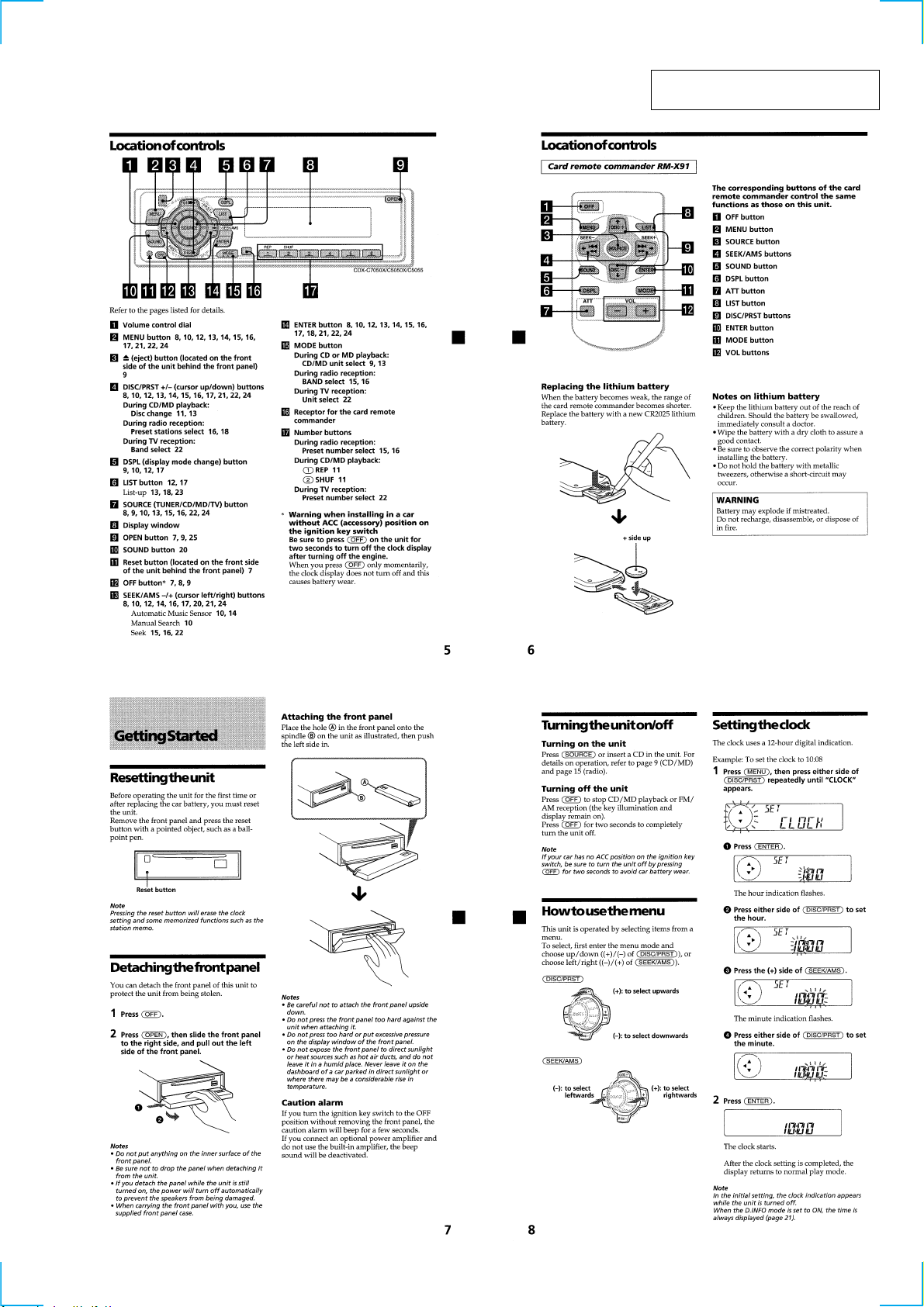
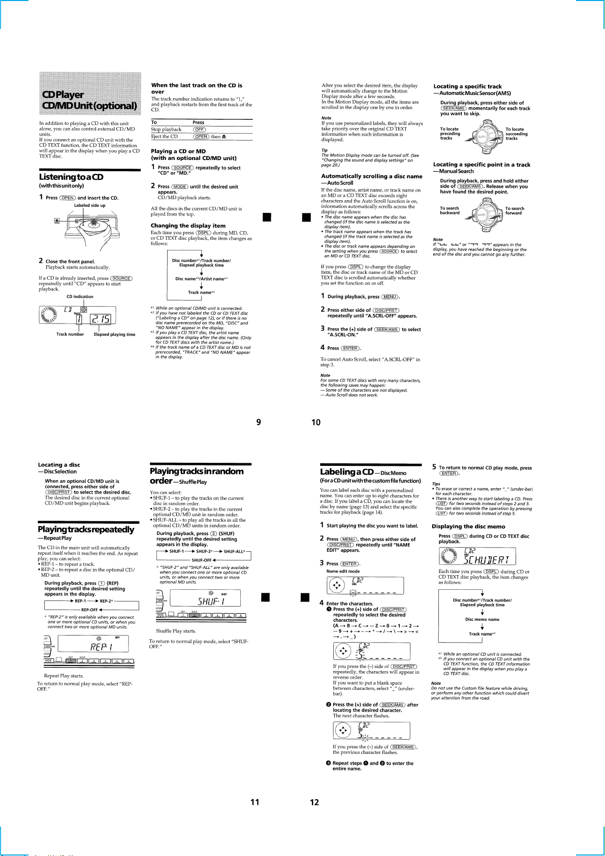
1. GENERAL
Location of controls................................................................. 3
Getting Started......................................................................... 3
Setting the clock ...................................................................... 3
CD Player CD/MD Unit (optional) ......................................... 4
Radio ....................................................................................... 5
Other Functions ....................................................................... 6
TV/Video (optional) ................................................................ 7
Connections ............................................................................. 8
2. DISASSEMBLY
2-1. Sub Panel (CD) Assy.........................................................10
2-2. CD Mechanism Block ....................................................... 10
2-3. Main Board ....................................................................... 11
2-4. Heat Sink ...........................................................................11
2-5. Chassis (T) Sub Assy ........................................................ 12
2-6. Lever Section..................................................................... 12
2-7. Servo Board....................................................................... 13
2-8. Shaft Roller Assy .............................................................. 13
2-9. Floating Block Assy .......................................................... 14
2-10. Optical Pick-up Block ....................................................... 14
3. DIAGRAMS
3-1. IC Pin Descriptions ........................................................... 15
3-2. Block Diagram –CD Section–........................................... 21
3-3. Block Diagram –Tuner Section–....................................... 22
3-4. Block Diagram –Display Section–.................................... 23
3-5. Circuit Boards Location .................................................... 23
3-6. Printed Wiring Boards –CD Mechanism Section–............ 24
3-7. Schematic Diagram –CD Mechanism Section (1/2)– ....... 26
3-8. Schematic Diagram –CD Mechanism Section (2/2)– ....... 27
3-9. Schematic Diagram –Main Section (1/2)– ........................ 28
3-10. Schematic Diagram –Main Section (2/2)– ........................ 29
3-11. Printed Wiring Board –Main Section– .............................. 30
3-12. Printed Wiring Board –Relay Section– ............................. 31
3-13. Schematic Diagram –Relay Section–................................ 32
3-14. Schematic Diagram –Display Section–............................. 33
3-15. Printed Wiring Board –Display Section– .......................... 34
3-16. IC Block Diagrams............................................................ 35
4. EXPLODED VIEWS
4-1. Chassis Section ................................................................. 38
4-2. Front Panel Section ........................................................... 39
4-3. CD Mechanism Section (1) ............................................... 40
4-4. CD Mechanism Section (2) ............................................... 41
4-5. CD Mechanism Section (3) ............................................... 42
5. ELECTRICAL PARTS LIST ........................................ 43
2
Page 3
SECTION 1
GENERAL
This section is extracted from
instruction manual (CDX-C7050X).
3
Page 4
45678910
Page 5
Page 6
Page 7
Page 8
Page 9
Page 10
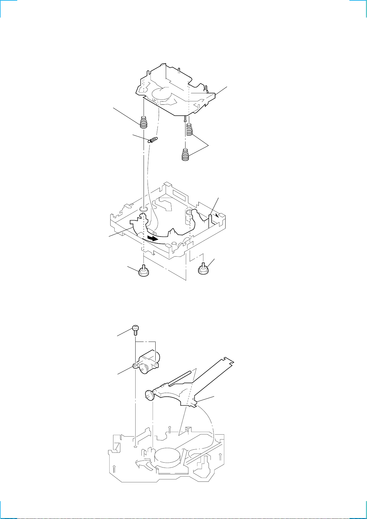
SECTION 2
DISASSEMBLY
Note : Follow the disassembly procedure in the numerical order given.
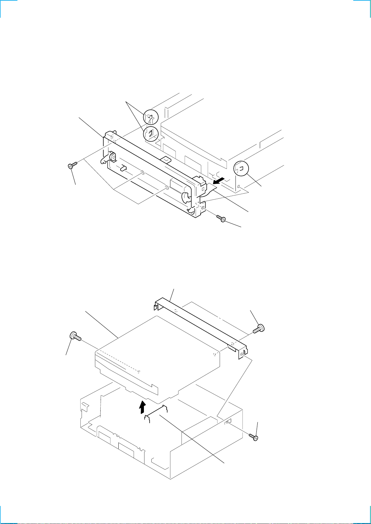
2-1. SUB PANEL (CD) ASSY
4 two claws
6 sub panel (CD) assy
2 PTT 2.6x6
2-2. CD MECHANISM BLOCK
5 CD mechanism block
2 PTT 2.6x6
3 claw
5 CNP800
1 PTT 2.6x6
7 bracket (CD)
6 PTT 2.6x6
3
1 PTT 2.6x6
4 CNP701
Page 11
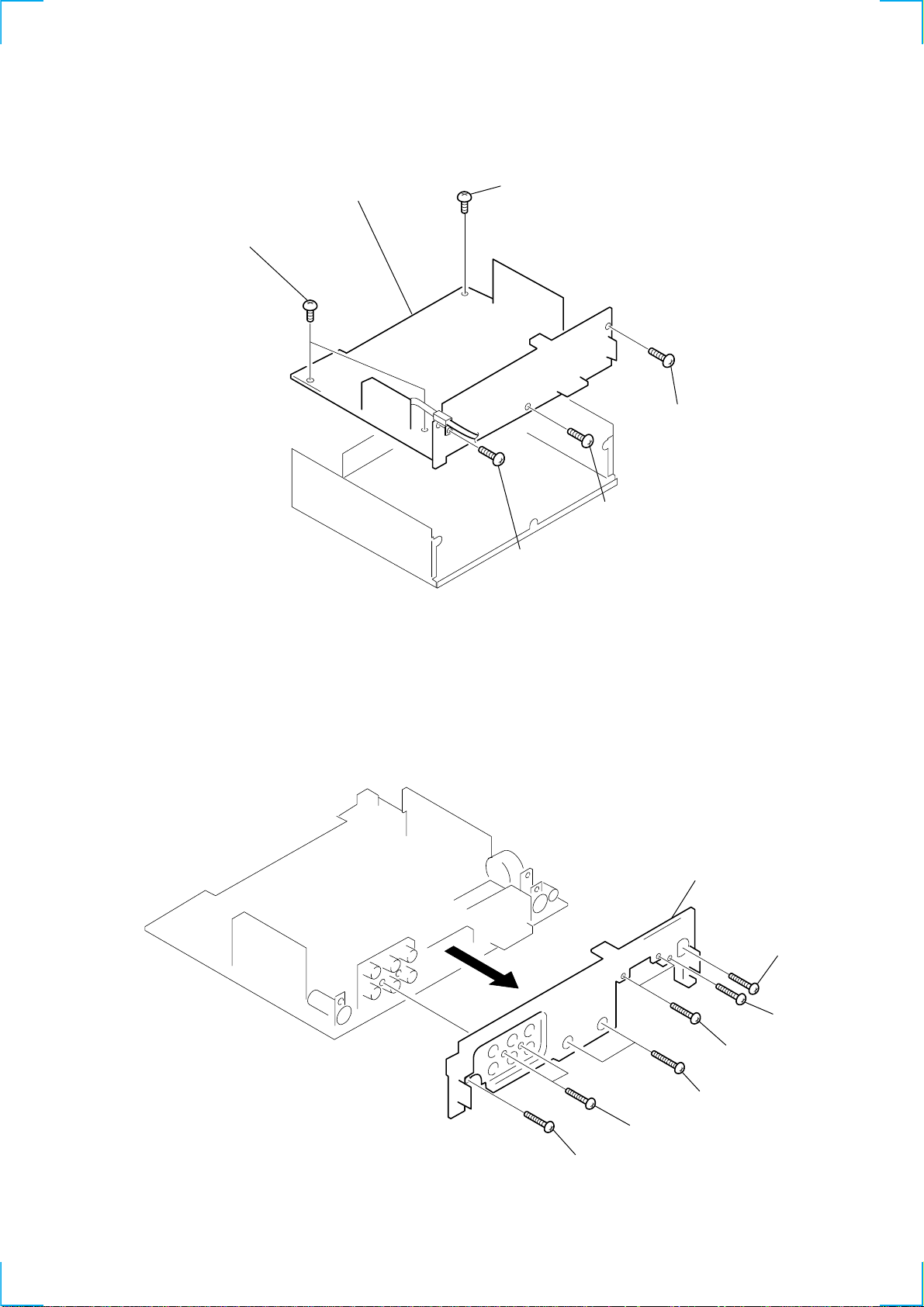
2-3. MAIN BOARD
5 PTT 2.6x6
6 MAIN board
4 PTT 2.6x6
3 PTT 2.6x8
2 PTT 2.6x8
1 PTT 2.6x8
2-4. HEAT SINK
7 heat sink
6 PTT 2.6x8
5 PTT 2.6x8
4 PTT 2.6x8
3 PTT 2.6x12
2 PTT 2.6x8
1 PTT 2.6x8
11
Page 12
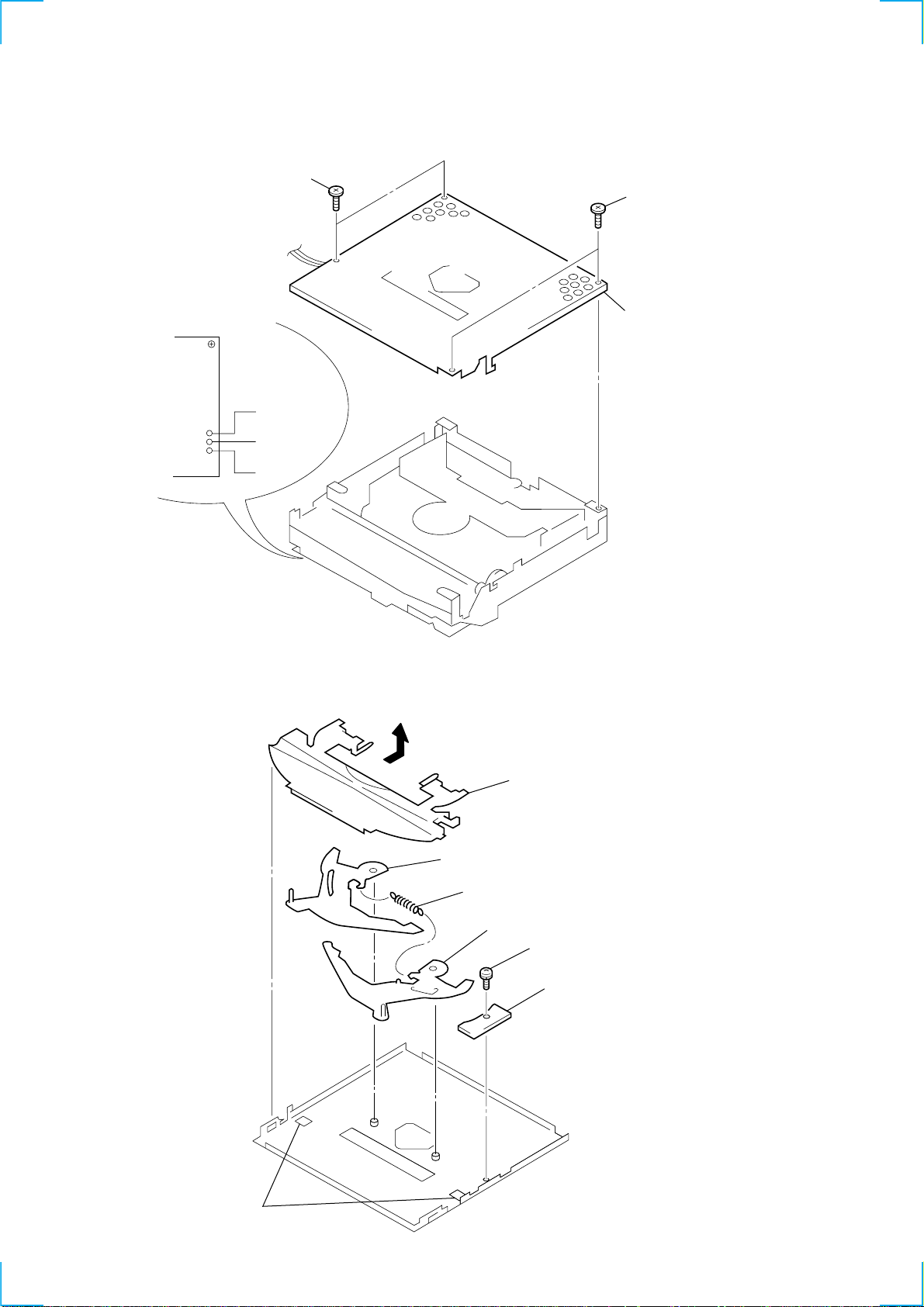
2-5. CHASSIS (T) SUB ASSY
2 P 2x3
3 P 2x3
1 Unsolder the
lead wires.
2-6. LEVER SECTION
4 chassis (T) sub assy
black
red
white
4 claws
5 guide (disc)
6 lever (R)
3 tension spring (LR)
7 lever (L)
1 screw
2 DISC IN SW board
12
Page 13
r
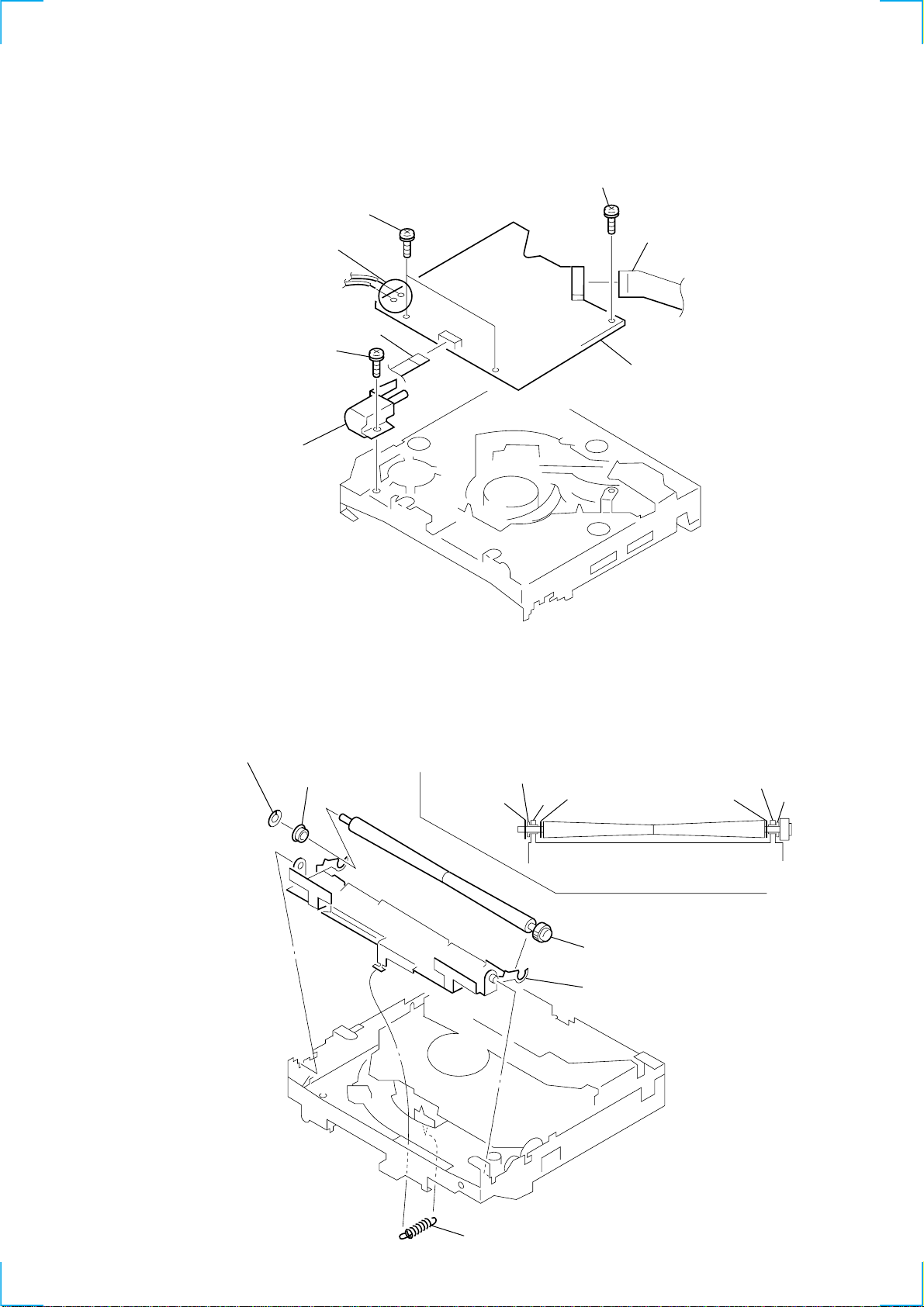
2-7. SERVO BOARD
7 PS 2x4
6 PS 2x4
3 Removal the solders.
4 P 2x3
5 loading motor assy
2-8. SHAFT ROLLER ASSY
• When installing, take note of the positions
arm (roller) and washers. (Fig. 1)
2 CN2
1 CN3
8 SERVO board
3 retaing ring (RA)
4 shaft retainer
shaft retainer
retaing ring (RA)
arm
washer
5 shaft roller assy
2 arm (roller)
Fig. 1
washer
arm
shaft retaine
1 tension spring (RA)
13
Page 14
2-9. FLOATING BLOCK ASSY
7 compression spring (FL)
1 tension spring (KF1)
6 floating block assy
8 compression spring (FL)
4 Fit lever (D) in the
direction of the arrow.
5 Turn loading ring in the
direction of the arrow.
3 damper (T)
2-10. OPTICAL PICK-UP BLOCK
1 P 2x3
2 sled motor assy
2 damper (T)
3 optical pick-up block
14
Page 15
SECTION 3
DIAGRAMS
3-1. IC PIN DESCRIPTIONS
• IC501 CXD2598Q (DIGITAL SERVO, DIGITAL SIGNAL PROCESSOR) (SERVO BOARD)
Pin No. Pin Name I/O Pin Description
1 DVDD — Digital power supply pin
2 DVSS — Digital ground
3 SOUT O Servo brock serial data output (Not used.)
4 SOCK O Servo brock serial data read clock output (Not used.)
5 XOLT O Servo brock serial data latch output (Not used.)
6 SQSO O Sub Q 80 bit, PCM peak and level data output. CD TEXT data output
7 SQCK I Clock input from SQSO read output.
8 SCSY I Fixed at “L”.
9 SBSO O Serial output of sub-P to W. (Not used.)
10 EXCK I Clock input from SBSO read output. (Fixed at “L”)
11 XRST I System reset (“L”: Reset)
12 STSM I System mute input (Fixed at “L”)
13 DATA I Serial data input from CPU.
14 XLAT I Latch input from CPU. Latch serial data at the falling edge.
15 CLOK I Serial data transfer clock input from CPU.
16 SENS O SENS output for CPU.
17 SCLK I Clock input from SENS serial data read.
18 ATSK I/O Input/output for anti-shock.
19 WFCK O WFCK (Write Flame Clock) output (Not used.)
20 XUGF O XUGF output (Not used.)
21 XPCK O XPCK output (Not used.)
22 GFS O GFS output
23 C2PO O C2PO output (Not used.)
24 SCOR O “H” output at either detection, sub code sync S0 or S1.
25 C4M O 4.2336 MHz output (Not used.)
26 WDCK O Word clock output f=2Fs (Not used.)
27 COUT I/O Track number count signal input/output (Not used.)
28 MIRR I/O Mirror signal input/output (Not used.)
29 DVSS — Digital ground
30 DVDD — Digital power supply pin
31 DFCT I/O Diffect signal input/output (Not used.)
32 FOK I/O Focus OK signal input/output
33 PWM1 I External control input of spindle motor.
34 LOCK I/O Lock signal input/output
35 MDP O Servo control output of spindle motor.
36 SSTP I Disc most inner track detection signal input
37 FSTIO I/O 2/3 frequency division input/output of pins ih and ij. (Not used.)
38 SFDR O Sled drive output
39 SRDR O Sled drive output
40 TFDR O Tracking drive output
41 TRDR O Tracking drive output
42 FFDR O Focus drive output
43 FRDR O Focus drive output
44 DVDD — Digital power supply pin
45 DVSS — Digital ground
46 TEST I Test pin (Fixed at “L”.)
47 TES1 I Test pin (Fixed at “L”.)
48 XTSL I X’tal select input (“L”: 16.9344 MHz, “H”: 33.8688 MHz)
49 VC I Center voltage input
50 FE I Focus error signal input
51 SE I Sled error signal input
15
Page 16
Pin No. Pin Name I/O Pin Description
52 TE I Tracking error signal input
53 CE I Center servo analog input
54 RFDC I RF signal input
55 ADIO O Test pin (Not used.)
56 AVSSO — Analog ground
57 IGEN I Constant current input from OP amplifier.
58 AVDDO — Analog ground
59 ASYO O EFM full-swing output (“L”: VSS, “H”: VDD)
60 ASYI I Asymmetry comparate voltage input
61 RFAC I EFM signal input
62 AVSS3 — Analog ground
63 CLTV I VCO control voltage input from master.
64 FILO O Filter output for master PLL (slave=digital PLL)
65 FILI I Filter input from master PLL.
66 PCO O Charge pump output for master PLL.
67 AVDD3 — Analog power supply pin
68 BIAS I Asymmetry circuit constant current input
69 VCTL I VCO2 control input from wideband EFM PLL. (Not used.)
70 V16M O VCO2 oscillator output for wideband EFM PLL. (Not used.)
71 VPCO O Charge pump output for wideband EFM PLL. (Not used.)
72 DVSS — Digital ground
73 MD2 I Digital out ON/OFF control input (“L”: OFF, “H”: ON)
74 DOUT O Digital out output
75 ASYE I Asymmetry circuit ON/OFF input (“L”: OFF, “H”: ON)
76 DVDD — Digital power supply pin
77 LRCK O D/A interface LR clock output (f=Fs)
78 LRCKI I D/A interface LR clock input
79 PCMD O D/A interface serial data output (2’s COMP, MSB fast)
80 PCMD I D/A interface serial data input (2’s COMP, MSB fast)
81 BCK O D/A interface bit clock output
82 BCKI I D/A interface bit clock input
83 EMPH O Emphasis ON/OFF signal output
84 EMPHI I Emphasis ON/OFF signal input (“H”: ON, “L”: OFF)
85 XVDD — Power supply for master clock.
86 XTAI I X’tal oscillator input from master clock (16.9344 MHz).
87 XTAO O X’tal oscillator output for master clock (16.9344 MHz).
88 XVSS — Ground pin for master clock.
89 AVDD1 — Analog power supply pin
90 AOUT1 O Lch analog output
91 AIN1 I Lch OPAMP input
92 LOUT1 O Lch LINE output
93 AVSS1 — Analog ground
94 AVSS2 — Analog ground
95 LOUT2 O Rch LINE output
96 AIN2 I Rch OPAMP input
97 AOUT2 O Rch analog output
98 AVDD2 — Analog power supply pin
99 RMUT O Rch “0” detect Flug (Not used.)
100 LMUT O Lch “0” detect Flug (Not used.)
16
Page 17
• IC5 CXP84640-072Q (CD SYSTEM CONTROL) (SERVO BOARD)
Pin No. Pin Name I/O Pin Description
1 ITRPT — Not used in this set.
2, 3 — — Not used in this set.
4, 5 NCO — Not used in this set.
6 OPEN I Front panel open detection input
7 CLOSE O Front panel close control output
8 LINKOFF I Bus interface link input
9 NCO — Not used in this set.
10 D SW I Down switch input (SW1)
11 SSTP I Limit switch input (SW4)
12, 13 NCO — Not used in this set.
14, 15 — — Not used in this set.
16 EMPH O O De-emphasis ON/OFF control output
17 CDMON O CD mechanism deck power control output
18 CD ON O CD power control output
19 A MUT O System attenuate control output
20 LD ON O Laser power ON/OFF control output
21 CD RST O CD system reset output
22 HOLD O Hold switch output
23 AGC CONT O AGC control output
24 — — Not used in this set.
25 PH3 I Not used in this set.
26 TSTIN0 I Not used in this set.
27 TSTIN1 I Not used in this set.
28 TST.CLV I Not used in this set.
29 NCO — Not used in this set.
30 RESET I System reset input (“L”=Reset)
31 X IN I X’tal oscillator input from system clock. (10 MHz)
32 X OUT O X’tal oscillator output for system clock. (10 MHz)
33 GND — Analog ground
34 XT OUT O Not used in this set.
35 XT IN I Not used in this set.
36 AVSS — A/D converter ground
37 AVREF I A/D converter reference voltage input
38 TEP L I Not used in this set.
39 TEP H I Not used in this set.
40 SLED– I Sled drive input
41 PH2 I Not used in this set.
42 SEK/SMET I Fixed at “H” in this set.
43 GFS/MNT2 SEL I Fixed at “H” in this set.
44 SC-JIG ON/OFF I Fixed at “H” in this set.
45 SCLK O CD-TEXT data read clock output
46 LOCK I/O Lock signal input/output
47 — — Not used in this set.
48 SCK2 O Sub Q read clock output
49 SI2 I Sub Q 80 bit, PCM peak and level data 16 bit input.
50 — — Not used in this set.
51 BUS CLK I/O Bus system serial clock input/output
52 BUS SI I Bus system serial interface input
53 BUS SO O Bus system serial interface output
54 F OK I Focus OK signal input
55 GFS I GFS signal detection input
56 TEST MODE I Fixed at “H” in this set.
17
Page 18
Pin No. Pin Name I/O Pin Description
57 SENS I SENS signal input
58 — — Not used in this set.
59 — — Not used in this set.
60 BU.IN I Back-up power detection input
61 BUSON I Bus on control input
62 IN SW I Disc in switch input (SW3)
63 SELF SW I Self switch input (SW2)
64 SCOR O Sub-code sync output
65 CD-CKO O CD signal process serial clock output
66 LM LOD O Loading motor control output
67 CD DATA O CD signal process serial data output
68 CD-XLAT O CD signal process serial data latch output
69 LM-EJ O Loading motor control output
70 DRV-OE O Focus/tracking coil/sled motor control output
71 MD2 O Digital out ON/OFF control output (“L”: OFF, “H”: ON)
72 VDD — Power supply pin
73 NIH I Fixed at “H” in this set.
74 V/Z I Fixed at “H” in this set.
75 PH1 I Not used in this set.
76 — — Not used in this set.
77 DOUT-SEL I Fixed at “H” in this set.
78 – 80 — — Not used in this set.
18
Page 19
• IC801 MN101C49KTB (SYSTEM CONTROL) (MAIN BOARD)
Pin No. Pin Name I/O Pin Description
1 VREF– — Ground for A/D converter power supply
2 S METER I S meter voltage detect signal input
3 FM AGC I FM auto gain control signal input
4 KEY IN1 I KEY signal input
5 KEY IN0 I KEY signal input
6 DSTSEL I Not used.
7 RC IN0 I Rotary commander signal input
8 FUNC SEL I Model function selection pin
9 NIL — Ground
10 VREF+ — A/D converter power supply
11 VDD — Power supply (+5 V) input pin
12 OSC OUT O High speed clock signal output (18.432 MHz)
13 OSC IN I High speed clock signal input (18.432 MHz)
14 VSS — Ground for power supply
15 XI I Low speed clock signal input (32 kHz)
16 XO O Low speed clock signal output (32 kHz)
17 MMOD — Not used. (Fixed at “L”.) Memory mode select signal input
18 RC IN1 I Rotary commander shift key signal input
19 SYSRST O System reset signal output
20 BUS ON O Bus on control signal output
21 LCD DATA O LCD serial data signal output
22 LCD CE O LCD chip enable signal output
23 LCD CLK O LCD serial clock signal output
24 ILL ON O Illumination power supply control signal output
25 DOOR IND O Control signal output for power on sub panel when open to front panel
26 KEY ACK I Key active interrupt detect signal input
27 NOSE I Front panel attachment detection input
28 BU IN I Back up power supply setect signal input
29 SIRCS I Remote control signal input
30, 31 NC — Not used. (Fixed at “L”.)
32 RAM — Not used.
33 RESET I Reset signal input
34 NC — Not used.
35 BEEP O Beep signal output
36 NC (FUNC SEL) I Model function selection pin
37 NC (FUNC SEL) I Model function selection pin
38 – 40 NC — Not used.
41 UNI CLI I Bus system serial clock signal input
42 UNI SO O Bus system serial interface signal output
43 UNI SI I Bus system serial interface signal input
44 UNI CLO O Bus system serial clock signal output
45 SDA I/O I2C bus serial data signal input/output
46 NC — Not used.
47 SCL O I2C bus serial clock signal output
48, 49 NC — Not used.
50 LOCK I Check when remove to lock of MDNO CLV SERVO
51 – 63 NC — Not used.
64 ACC IN I Accessory power supply voltage detection input
65 TEL MUT I Telephone attenuate detect signal input
66 TEST IN I Test mode setting detect first stage signal input
67 ANT CUT — Not used.
68 NC — Not used.
19
Page 20
Pin No. Pin Name I/O Pin Description
69 AMP ON O Power supply on/off control signal output
70 MUT O System attenuate control signal output
71 AMP MUT O Power amp attenuate control signal output
72 VOL MUT O Mute control signal output for electrical volume
73 TU ON O Tuner attenuate signal output
74 EEP SDA I/O Tuner EEPROM serial data signal input/output
75 EEP SCL O Runer EEPROM serial clock signal output
76 IF BW I Not used.
77 NC — Not used. Tuner switch VCO level shift signal input
78 NC — Not used.
79 REIN1 I Rotary encoder signal input
80 REIN0 I Rotary encoder signal input
81 AD ON O Power control output for A/D conversion
82 – 92 NC — Not used.
93 OPEN I Front panel open/close condition signal input
94 – 98 NC — Not used.
99 PW ON O System power supply control signal output
100 NC — Not used.
20
Page 21

CDX-C7000X/C7050X
TUNER
SECTION
(Page 22)
B
ATT
IC801 (1/3)
OPEN93MUT
SYSTEM CONTROL
70
BATT
213
8
7
SIRCS
C
BATT
10 3
CHECK
RESET
13 2
Q801
1
BUS ON
12
DATA
9
SECTION
DISPLAY
(RESET)
(Page 23)
IC802
BUS INTERFACE
BATT (L)
BU 5V
IC902
RESET
BU IN28SYS RST
BUS ON
UNI SO42UNI SI43UNI CLO44UNI CLI
41
33
19
20
RESET
3 1
S900
BUS
CNP801
546
6
CONTROL IN
4
CLK
8
11
Q803
: CD
• Signal path
(Page 22)
IC501
DIGITAL SERVO,
DIGITAL SIGNAL PROCESSOR
TUNER
SECTION
A
CD L
92
LOUT1
LOUT2
D/A
D/A
EFM
61
16
RFO RFAC
RF
95
CONV.
I/F
DEM
EQ
IC5
CD SYSTEM CONTROL
R-CH
LOCK
DIGITAL
RFDC
54
19
A MUT
LOCK
46
34
CLV
6
OPEN
(DISPLAY BOARD)
SI2
48
49
6
7
SQCK
SQSO
SUB
CODE
FE
TE
525150
13
14
FE
TE
51
BUS CLK
SCOR64SCK2
24
SCOR
PROCESS
SE
52
BUS SI
71
73
MD2
61
BUS ON
CD RST21MD2
XRST11DATA
222120
LD ON
30
60
BU IN
RESET
CD DATA
68
67
13
14
XLAT
HOLD SW
AGC CONT
17
SCLK
16
CLOK15SENS
X1
10MHz
31
32
X IN
X OUT
FOK54GFS55SENS57CD CKO65SCLK45CD XLAT
X2
16MHz
32
86
87
GFS22FOK
XTALI
XTALO
SERVO
FFDR
FRDR
TFDR
42434041383935
CTL
TRDR
SSTP
11
SW4
(LIMIT)
SFDR
D SW
10
SW1
(DOWN)
SRDR
IN SW
62
SW3
SELF SW
63
SW2
(DISC IN)
MDP
LM EJ
LM LOD66SLED –40DRIVE ON70LD ON20HOLD22AGC CONT23CD ON18CDM ON
69
(SELF)
CD ON
CD MECHA ON
SWITCH
Q701, 702
17
SWITCH
Q903, 913
53
BUS SO
BATT
+11V REG
REG
CD +6V
REG
CD +5V
CD +5V
8
LNK OFF
Q920
21 21
Q922
Q703
CD +6V
IC1
ERROR AMP
RF AMP, LD APC,
FOCUS
ERROR
D
B
C
A
7
6
5
KSS-720A
A
OPTICAL PICKUP
8
I-V
CONV.
C
B
D
3-2. BLOCK DIAGRAM — CD SECTION —
TRACKING
E
F
11
E
ERROR
10
F
1
22
21
25
31
24
32
LD
AMP
LD
PD
4
LD
PD
IC7
3
TRACKING/FOCUS COIL DRIVE
SLED/SPINDLE/LOADING MOTOR DRIVE
Q101
DRIVE
LD
FOCUS
10
FOCUS
COIL
COIL
DRIVE
11
COIL
TRACKING
8
COIL
TRACKING
DRIVE
9
SLED
M902
6
DRIVE
MOTOR
7
SLED
MOTOR
SPINDLE
12
M901
18
DRIVE
MOTOR
13
MOTOR
SPINDLE
MOTOR
LOADING
5
M903
LOADING
2
DRIVE
4
MOTOR
34
MUTE 1
35
MUTE 2
04
Page 22

(M0N0)
CNP401
SUB OUT
-1L-2
H
C
R
MUTE
IC406
26
OUTSWL
IC701
ELECTRONIC VOLUME
R
AUDIO OUT FRONT
PJ400(2/2)
AUDIO OUT REAR
Q403
R
L
L R
C7000X
–1 –2
–3 –4
CNP501
IC101
POWER AMP
H
H
C7050X
IC402
LINE OUT(LCH)
FL+
192
539
12
C
-
R
C
-
R
13
OUT FL
INFL
2
30
OUT LF
AUX L
3
FL–
CD L
1
RL+
RL–
FR+
4
10
8
11
Q101
MUTE
12
OUT RLINRL
7
29
OUT LR
MPXAMAM IF
11
13
FR–
RR+
3
12
R-CH
MUTE
STAND BY
4
22
Q102
MUTE
C7000X
LEVEL
MPIN
1214152021
BATT
RR–
16
11
F901
BATT
B
CD
SECTION
ATT
MUTE
SWITCH
Q401, 402
IC801 (2/3)
SYSTEM CONTROL
SDA
SCL
MUTE
18
(Page 21)
35
69
BEEP
AMP ON
VOL MUT
72
ATT
13
TEL
Q916
MUTE
71
65
TEL MUT
AMP MUTE
TEST
BATT
15
AMP REM6ANT REM
5
Q921
AMP +B
SWITCH
TU ON
Q902
SWITCH
TU +5V
: FM
: AM
: CD
ACC
7
• Signal path
REG
Q601
73
TU ON
TU +5V
TU +8V
TU +8V
COM +8V
COM +8V
REG
REG
BATT
Q602
Q904
Q907
TU ON
Q603
SWITCH
PW ON
Q919
SWITCH
SWITCH
DOOR IND
25
DOOR IND
FM AGC
3
Q908
EEP SDA
EEP SCL
75
74
Q906
BATT
CHECK
ACC
Q905
CHECK
64
ACC IN
S-MRTER
2
IC901
POWER SUPPLY
66
TEST IN
SDA
SCL
45
47
VCC AMP +B
4 2
BATT
PULL UP +5V
BACKUP +5V
5
3
GND
BU +B
AMP ON
1
99
PW ON
H
C
-
R
L R
PJ400(1/2)
BUS AUDIO IN
–5 –6
CDL
A
CD
SECTION
(Page 21)
TU601
TUNER UNIT
ANTFM MPX
2 10
CNJ600
3-3. BLOCK DIAGRAM — TUNER SECTION —
(ANTENNA)
8
AM DET
ANTAM
1
19
AM IF
14
12
SDA
S-METER
2222
TU +8V
BACKUP +5V
TU +5V
4
13
SCL
5
11
IF BW
VDD (8V)
16
VDD (5V)
FM AGC
17
18
SCL (EEP)
SDA (EEP)
04
CDX-C7000X/C7050X
Page 23

tuner unit
(TU601)
CDX-C7000X/C7050X
LIMIT SW board
3-5. CIRCUIT BOARDS LOCATION
DISC IN SW board
RELAY board
MAIN board
SERVO board
DISPLAY board
DISPLAY PANEL
LIQUID CRYSTAL
I
4
51•52I55
S04IS51
IC901
LCD DRIVE
64
LCD DATA
IC801 (3/3)
SYSTEM CONTROL
KEY IN0 DATA
5 21
LCD901
COM1ICOM4
CE
62
22
LCD CE
CL
63
2347
LCD CLK
KEY IN1
KEY
KEY ACK
26
Q914
ACTIVE
AD ON
81
KEY
KEY ACT
Q915
ACTIVE
F/P +10V
RC IN1
18
RC IN0
7
IC951
LSW910-916
LED910-915 LSW901-909
SIRCS
29
IR
RECEIVE
Q802
LED921-924
Q911
CONT
POWER
24
ILL ON
RE IN0
RE IN1
8079271615
RE901
ROTARY
ENCODER
ILL +B
Q912
+10V REG
BATT
NOSE
S901
X800
14.432MHz
12
OSC OUT
XO
X801
(NOSE DET)
23 23
13
OSC IN
XI
32.768kHz
3-4. BLOCK DIAGRAM — DISPLAY SECTION —
KEY MATRIX
LSW901-909
LSW910-916
S901-904
CNP802
(REMOTE IN)
SIRCS
C
CD
SECTION
04
(Page 21)
Page 24

3-6. PRINTED WIRING BOARDS — CD MECHANISM SECTION —
W or less unless otherwise
4
/
1
2424
THIS NOTE IS COMMON FOR PRINTED WIRING
BOARDS AND SCHEMATIC DIAGRAMS.
(In addition to this, the necessary note is
50 WV or less are not indicated except for electrolytics
printed in each block.)
for schematic diagram:
• All capacitors are in µF unless otherwise noted. pF: µµF
CDX-C7000X/C7050X
: internal component.
f
specified.
and tantalums.
• % : indicates tolerance.
•
• All resistors are in Ω and
with mark 0 are critical for safety.
Replace only with part number specified.
supply from ACC and BATT cords.
Voltage variations may be noted due to normal produc-
Note: The components identified by mark 0 or dotted line
• C : panel designation.
• U : B+ Line.
tion tolerances.
• Power voltage is dc 14.4V and fed with regulated dc power
• Voltages are taken with a V OM (Input impedance 10 MΩ).
Voltage variations may be noted due to normal produc-
tion tolerances.
F : FM
f : AM
• Waveforms are taken with a oscilloscope.
J : CD
• Circled numbers refer to waveforms.
• Signal path.
for printed wiring boards:
: Through hole.
a
(The other layer’s patterns are not indicated.)
Caution:
Pattern face side: Parts on the pattern face side seen from the
(Side B) pattern face are indicated.
Parts face side: Parts on the parts face side seen from the
• X : parts extracted from the component side.
• Y : parts extracted from the conductor side.
•
• b : Pattern from the side which enables seeing.
(Side A) parts face are indicated.
Page 25

CDX-C7000X/C7050X
Ref. No. Location
IC1 C-1
IC5 C-6
Location
• Semiconductor
IC7 F-2
IC501 F-5
Q101 B-2
(Page 30)
25 25
Page 26

(Page 27)
(Page 28)
(Page 27)
2626
0V
0V
1.2Vp-p
KSS-720A
CDX-C7000X/C7050X
3-7. SCHEMATIC DIAGRAM — CD MECHANISM SECTION (1/2) — • Refer to page 35 for IC Block Diagrams.
(TE)
qd
IC1
Approx. 200mVp-p
(FE)
qf
IC1
Approx. 620mVp-p
(RFO)
qh
IC1
: Impossible to measure
∗
with respect to ground
under no-signal conditions.
1
• Waveforms (MODE:PLAY)
2
3
Note:
• Voltage and waveforms are dc
no mark : CD PLAY
Page 27

CDX-C7000X/C7050X
(Page 26)
(Page 26)
: Impossible to measure
∗
under no-signal conditions.
no mark : CD PLAY
Note:
• Voltage and waveforms are dc with respect to ground
27 27
3-8. SCHEMATIC DIAGRAM — CD MECHANISM SECTION (2/2) — • Refer to page 36 for IC Block Diagrams.
Page 28

(Page 29)
(Page 32)
(detuned) condition.
no mark : FM
(): AM
Note:
< > : CD PLAY
• Voltage is dc with respect to ground under no-signal
26)
(Page
2828
3-9. SCHEMATIC DIAGRAM — MAIN SECTION (1/2) — • Refer to page 35 for IC Block Diagrams.
CDX-C7000X/C7050X
Page 29

CDX-C7000X/C7050X
under no-signal (detuned) condition.
no mark : FM
(): AM
• Voltage is dc with respect to ground
< > : CD PLAY
Note:
29 29
3-10. SCHEMATIC DIAGRAM — MAIN SECTION (2/2) — • Refer to page 35 for IC Block Diagrams.
(Page 28)
Page 30

D926 C-7
D927 C-7
D928 C-7
D930 D-10
IC101 B-8
(IC401) E-4
D405 F-7
(IC402) F-4
D601 I-1
D603 I-2
D701 E-14
D702 I-5
Ref. No. Location
Ref. No. Location
D401 G-8
D402 H-7
D404 C-5
• Semiconductor Location
IC406 D-6
D801 H-9
IC701 H-4
D802 H-10
IC801 I-8
D803 D-12
IC802 F-11
D806 D-12
IC901 F-13
D807 F-12
IC902 J-12
D808 E-11
D809 D-12
Q101 C-5
D810 J-3
Q102 C-3
D811 J-3
Q201 C-5
D812 J-3
Q202 C-4
D813 J-3
Q401 G-6
D814 J-3
Q402 G-7
D815 J-3
Q403 D-4
D816 J-4
Q601 I-1
Q602 J-2
Q603 J-1
Q701 E-13
Q702 F-13
Q703 D-13
Q801 E-11
Q802 E-10
Q803 F-11
Q902 D-7
Q903 C-14
Q904 H-14
Q905 E-7
Q906 F-8
Q907 I-13
Q908 H-12
Q911 K-13
Q912 I-12
Q913 C-14
Q914 K-7
Q915 J-5
Q916 E-7
Q919 I-12
Q920 B-13
Q921 C-10
Q922 G-14
D817 J-4
D818 J-4
D820 G-10
D821 F-11
D822 B-14
D823 B-13
D901 B-11
D902 D-11
D903 C-11
D904 G-12
D905 H-14
D906 I-14
D907 E-12
D909 F-12
D910 F-8
D911 D-7
D913 K-8
D914 D-8
D915 J-5
D917 D-7
D918 B-14
D921 C-8
D922 C-8
D923 C-8
D924 C-8
D925 C-7
( ) : CDX-C7050X only
(Page 25)
3030
(Page 31)
3-11. PRINTED WIRING BOARD — MAIN SECTION —
CDX-C7000X/C7050X
Page 31

CDX-C7000X/C7050X
(Page 30)
(Page 34)
31 31
3-12. PRINTED WIRING BOARD — RELAY SECTION —
Page 32

(Page 28)
3232
3-13. SCHEMATIC DIAGRAM — RELAY SECTION —
CDX-C7000X/C7050X
(Page 33)
Page 33

CDX-C7000X/C7050X
(detuned) condition.
no mark : FM
Note:
• Voltage is dc with respect to ground under no-signal
33 33
3-14. SCHEMATIC DIAGRAM — DISPLAY SECTION —
(Page 32)
Page 34

Ref. No. Location
LED911 A-13
LED912 A-5
LED913 B-5
LED914 B-13
LED915 B-5
LED921 A-2
LED922 C-2
Ref. No. Location
(D902) B-10
(D903) B-10
(D905) A-6
(D951) C-5
(IC901) B-8
• Semiconductor Location
(Page 31)
IC951 C-6
LED923 C-4
LED924 A-4
LED910 B-13
( ) : SIDE B
3434
3-15. PRINTED WIRING BOARD — DISPLAY SECTION —
CDX-C7000X/C7050X
Page 35

REFERENCE
REFERENCE
VCC
VCCL
VCCL
INL
SVRL
INML
INMR
SVRR
INR
VCCR
VCCR
VCCR
BUFFER
BUFFER
BUFFER
BUFFER
LIFT
AMP
SIGNAL
AMP
LIFT
AMP
SIGNAL
AMP
CL+
CL–
LGND
OUTL
OUTR
RGND
CR–
CR+
16
15
14
13
12
11
10
9
8
7
6
5
4
3
2
1
3-16. IC BLOCK DIAGRAMS
IC1 CXA2596M-T6
IC401, 402 NJM2160AM-TE2
(CDX-C7050X only)
APC PD AMP
HOLD
1 24
VEE
AGCVTH
2
VEE
1.25V
VREF
LD
3
PD
4
A
5
B
6
C
7
D
8
VEE
VC
VEE
9
+
VC
VC
VC BUFFER
–
–
+
+
–
F
10
E
11
12
VC
IC901 BA4903ST-V5
5.7V
ON ON
+–
+
–
+
–
–
+
VC
VCC
VEE
VCC
+
–
+
–
VC
+
–
+
–
+
–
RF SUMMING AMP RF EQ AMP
VC
VC
VC
+–
VC
+
–
VEE
ERROR AMP
+
–
APC LD AMP
VCC
+
–
FOCUS
+
–
VC
ERROR AMP
VC
VCC
–
+
TRACKING
23
22
21
20
19
18
17
16
15
14
13
VCC
LC/PD
LD ON
HOLD SW
AGCCONT
RF BOT
RFTC
RF I
RFO
RFE
FE
TE
IC802 BA8270F-E2
BUS ON
1
OUT
RST
2
OUT
BATT
3
CLK
4
OUT
5
VREF
6
DATA
IN/OUT
GND
7 8
BUS ON
SWITCH
RESET
SWITCH
BATTERY
SWITCH
14
13
12
11
10
9
VCC
RST
BUS ON IN
CLK IN
BATT
CHECK
DATA IN
DATA OUT
AMPONAMP
CIRCUIT ON
B+
THERMAL
SHUT
DOWN
GND VCC BU+B
REGULATOR
VREF
OVER
VOLTAGE
PROTECT
51 2 3 4
35
Page 36

IC7 LA6556
FWD
REV
VCC2
VL0–
VL0+
VO4+
VO4–
VO3+
VO3–
VO2+
VO2–
MUTE2
MUTE1
VIN1/VREF SW
5V REG
+
–
GND
+
–
–
+
36
S-GND
35
MUTE2
34
MUTE1
VIN4
33
VIN4–
32
VIN4+
31
VREF-IN
30
VIN1 (VREF)-SW
29
VREF-OUT (CH1)
28
REG-OUT
27
REG-IN
26
1
INPUT
2
3
4
5
6
7
8
9
10
11
OUTPUT
CONTROL
LEVEL
SHIFT
LEVEL
SHIFT
–
+
LEVEL
SHIFT
CH2-CH4 OUTPUT
ON/OFF
CH1 OUTPUT
ON/OFF
–
+
VO1+
VO1–
VCC1
VIN1
VIN1–A
VIN1+A
VIN1–B
12
13
14
15
16
AMP-A
–
+
17
–
18
+
AMP-B
LEVEL
SHIFT
–
+
–
+
–
+
VIN3+
25
+
–
VIN3–
24
VIN3
23
VIN2+
22
+
–
VIN2–
21
20
VIN2
19
VIN1 +B
36
Page 37

IC701 TDA7402TR
ACINLR
ACINLR
ACINRR
OUTLF
33
OUTLR
28 2730 2932 31
OUTRF
OUTRR
OUTSWL
OUTSWR
26 25 24 23
OUTSSL
OUTSSR
ACINLF
SWINR
SWINL
AC OUTR
AC OUTL
VREF
MUX
MD1 (SE4L)
MD1G (SE4R)
MD2
MD2G
MONO
FADER
MIXER
MIXING
SUBWOOFER
+PHASE
CONTROL
SECOND SOURCE
LOUDNESS
IN GAIN
MUTE
SELECTOR
II
C-BUS
DIGITAL
CONTROL
BEEP
HIGH OUT
S & H
LP
DEMODULATOR
+STEREO ADJUST
+STEREO BLAND
PILOT
CANCELLATION
LP
PIL, DET
PLL
QUAL.
MALTI
PATH
DETECTOR
MONO
FADER
34
35
36
37
38
LP
HP
BASS
39
40
41
42
43
44
TRABLE
VOLUME
SOFT MUTE
LOUDNESS COMPANDER
IN GAIN
+ AUTO
ZERO
MAIN SOURCE
SELECTOR
OUTPUT CONTROL
VOICE
BANDPASS
INPUT MULTIPLEXER
MONO
FADER
SELECTOR
SUPPLY
D/A
PULSE
FORMER
AM/FM
NOISE
BLANKER
22
21
20
19
18
17
16
15
14
13
12
VDD
SCL
SDA
GND
MUTE
QUAL
MP OUT
MP IN
LEVEL
MPX
AMIF
1 2 3 4 5 6 7 8 9 10 11
CD L
CD R
SE2L
SE2R
AUX L
AUX R
FD2L+
FD2L–
FD2R+
FD2R–
AM
37
Page 38

NOTE:
• The mechanical parts with no reference
number in the exploded views are not supplied.
• Items marked “*” are not stocked since
they are seldom required for routine service.
Some delay should be anticipated
when ordering these items.
• -XX and -X mean standardized parts, so
they may have some difference from the
original one.
4-1. CHASSIS SECTION
SECTION 4
EXPLODED VIEWS
• Color Indication of Appearance Parts
Example :
KNOB, BALANCE (WHITE) ... (RED)
R
Parts Color Cabinet’s Color
• Accessories and packing materials and
hardware (# mark) list are given in
the last of this parts list.
The components identified by
mark 0 or dotted line with mark
R
0 are critical for safety.
Replace only with part number
specified.
#2
9
MG-383Z-121//K
#2
8
11
15
10
16
14
13
#1
#1
#1
#2
#1
#3
20
#1
#1
#1
#1
12
TU601
4
3
19
#1
F901
11
2
1
5
#2
7
6
#5
#2
#5
#5
18
Ref. No. Part No. Description Remark
1 X-3378-387-1 PANEL ASSY (CD), SUB
2 3-041-039-01 BUTTON (EJECT)
* 3 1-676-690-11 RELAY BOARD
4 X-3376-686-2 GEAR ASSY
5 3-030-909-02 DAMPER, OIL
6 X-3376-687-1 LOCK ASSY
7 3-713-786-51 SCREW +P 2X3
* 8 3-041-156-01 COVER
9 1-792-194-21 CORD (WITH CONNECTOR) (POWER)
* 10 3-041-173-01 BRACKET (CD)
11 3-376-464-11 SCREW (+PTT 2.6X6), GROUND POINT
* 12 A-3294-934-A MAIN BOARD, COMPLETE (C7050X)
#2
#2
17
Ref. No. Part No. Description Remark
* 12 A-3294-935-A MAIN BOARD, COMPLETE (C7000X)
* 13 3-019-565-01 BRACKET (IC)
* 14 3-041-157-11 HEAT SINK (6P)
* 15 3-041-174-01 HEAT SINK (REG)
* 16 3-041-261-01 BRACKET (TR)
* 17 3-041-155-01 CHASSIS
18 3-035-250-02 SCREW (LOCK)
* 19 X-3376-689-1 BRACKET (GEAR) ASSY
20 1-790-375-21 CORD (WITH CONNECTOR) (SUB OUT (MONO))
F901 1-532-877-11 FUSE (BLADE TYPE) (AUTO FUSE) 10A
TU601 A-3220-738-A TUNER UNIT (TUX-020)
38
Page 39

4-2. FRONT PANEL SECTION
#4
#4
57
#4
not supplied
(DISPLAY board)
55
66
65
LCD901
53
52
51
51 3-041-028-01 BUTTON (SOURCE)
52 3-041-029-01 KNOB (VOL)
53 3-041-030-01 BUTTON (CROSS)
54 3-042-967-01 CUSHION (CROSS)
* 55 X-3378-426-1 HOLDER (LCD) ASSY
54
64
63
61
62
59
58
67
56
Ref. No. Part No. Description RemarkRef. No. Part No. Description Remark
60 3-041-036-01 BUTTON (1-6/M)
61 3-041-033-01 BUTTON (LIST/ENTER)
62 3-041-035-01 BUTTON (OFF)
63 3-041-034-01 BUTTON (MENU/SOUND)
* 64 3-041-175-01 PLATE (LCD), GROUND
60
56 X-3378-607-1 PANEL (S) ASSY, FRONT (C7000X)
56 X-3378-609-1 PANEL (S) ASSY, FRONT (C7050X)
57 X-3378-391-1 PANEL ASSY, FRONT BACK
58 3-041-037-01 BUTTON (OPEN)
59 3-032-321-01 SPRING (OPEN)
65 1-694-660-11 CONDUCTIVE BOARD, CONNECTION
* 66 3-041-372-01 SHEET (REFLECTOR)
67 3-041-038-01 BUTTON (D) (C7000X)
LCD901 1-803-907-31 DISPLAY PANEL, LIQUID CRYSTAL (C7000X)
LCD901 1-803-909-21 DISPLAY PANEL, LIQUID CRYSTAL (C7050X)
39
Page 40

4-3. CD MECHANISM SECTION (1)
(MG-383Z-121//K)
101
115
104
114
109
116
103
#8
102
#8
107
106
105
111
114
113
108
C
M903
#7
#7
110 3-040-040-01 ARM (ROLLER)
* 111 A-3294-809-A SERVO BOARD, COMPLETE
* 112 3-040-048-01 BRACKET (MOTOR)
113 3-040-034-01 SPRING (RA), TENSION
114 3-040-042-01 WASHER
#8
#9
112
105
C
110
Ref. No. Part No. Description Remark Ref. No. Part No. Description Remark
* 101 1-676-709-11 DISC IN SW BOARD
102 3-040-039-01 CHASSIS (T)
103 3-040-038-01 SPRING (LR), TENSION
104 3-040-050-01 LEVER (L)
105 3-040-022-01 RETAINER (RA), SHAFT
106 3-040-044-01 ROLLER (S)
107 3-040-067-01 LEVER (R)
108 A-3301-980-A SHAFT ROLLER ASSY
109 3-040-037-01 GUIDE (DISC)
40
115 3-043-880-01 RING (RA), RETAINING
116 3-043-499-01 SCREW
M903 A-3315-039-A MOTOR SUB ASSY, LO (LOADING)
Page 41

4-4. CD MECHANISM SECTION (2)
(MG-383Z-121//K)
157
158
163
154
162
D
160
165
151
156
157
164
155
153
161
D
159
152
152
152
Ref. No. Part No. Description Remark Ref. No. Part No. Description Remark
151 3-040-025-01 ARM, CHUCKING
152 3-040-031-01 DAMPER (T)
153 3-040-056-01 LEVER (D)
154 3-040-024-01 RETAINER (DISC)
155 3-040-053-01 RING, LOADING
159 A-3307-422-A CHASSIS (M) COMPLETE ASSY
160 3-040-059-01 SPRING (TR), TENSION
161 3-040-057-01 LEVER (LOCK)
162 3-040-058-01 GEAR (MDL)
163 3-040-052-01 WHEEL (U), WORM
156 3-040-026-01 SPRING (CH), TENSION
157 3-040-032-01 SPRING (FL), COMPRESSION
158 3-040-033-01 SPRING (KF1), TENSION
164 3-040-051-01 LEVER (TR)
165 3-040-054-01 WHEEL (LW), WORM
41
Page 42

4-5. CD MECHANISM SECTION (3)
(MG-383Z-121//K)
201
M901
207
209
206
208
202
M902
203
#6
210
204
#8
205
211
#8
The components identified by
mark 0 or dotted line with mark
0 are critical for safety.
Replace only with part number
specified.
Ref. No. Part No. Description Remark Ref. No. Part No. Description Remark
* 201 X-3378-480-1 CHASSIS (OP) ASSY (INCLUDING M901)
202 3-040-029-01 SPRING (SL), TORSION
203 3-040-045-01 BASE (DRIVING)
204 3-040-194-01 GEAR (SL MIDWAY)
205 A-3301-983-A SHAFT (FEED) ASSY
206 1-676-707-11 PICK-UP FLEXIBLE BOARD
207 1-677-182-11 MOTOR FLEXIBLE BOARD
* 208 1-676-708-11 LIMIT SW BOARD
209 3-909-607-01 SCREW
0210 8-820-103-03 PICK-UP, OPTICAL KSS-720A/K1RP
211 3-040-030-01 SPRING (FEED), PLATE
M902 A-3301-985-A MOTOR ASSY, SLED (SLED)
42
Page 43

SECTION 5
ELECTRICAL PARTS LIST
NOTE:
• Due to standardization, replacements in
the parts list may be different from the
parts specified in the diagrams or the
components used on the set.
• -XX and -X mean standardized parts, so
they may have some difference from the
original one.
• RESISTORS
All resistors are in ohms.
METAL:Metal-film resistor.
METAL OXIDE: Metal oxide-film resistor.
F:nonflammable
Ref. No. Part No. Description Remark Ref. No. Part No. Description Remark
* 1-676-709-11 DISC IN SW BOARD
****************
< SWITCH >
SW2 1-529-566-21 SWITCH, PUSH (1 KEY) (SELF)
SW3 1-529-566-21 SWITCH, PUSH (1 KEY) (DISC IN)
*************************************************************
DISPLAY BOARD
**************
1-694-660-11 CONDUCTIVE BOARD, CONNECTION
* 3-041-175-01 PLATE (LCD), GROUND
* 3-041-372-01 SHEET (REFLECTOR)
• Items marked “*” are not stocked since
they are seldom required for routine service.
Some delay should be anticipated
when ordering these items.
• SEMICONDUCTORS
In each case, u : µ, for example:
uA.. : µA.. uPA.. : µPA..
uPB.. : µPB.. uPC.. : µPC.. uPD.. : µPD..
• CAPACITORS
uF : µF
• COILS
uH : µH
LED914 8-719-078-19 LED LWA673-R1S2
LED915 8-719-078-19 LED LWA673-R1S2
LED921 8-719-078-83 LED SML-310VT
LED922 8-719-078-83 LED SML-310VT
LED923 8-719-078-83 LED SML-310VT
LED924 8-719-078-83 LED SML-310VT
LSW901 1-771-883-11 SWITCH, TACTILE (WITH LED) (OFF)
LSW902 1-771-476-11 SWITCH, KEY BOARD (WITH LED) (SOURCE)
LSW903 1-771-476-11 SWITCH, KEY BOARD (WITH LED) (SOUND)
LSW904 1-771-476-11 SWITCH, KEY BOARD (WITH LED) (MENU)
LSW905 1-771-476-11 SWITCH, KEY BOARD (WITH LED) (DSPL)
DISC IN SW DISPLAY
The components identified by
mark 0 or dotted line with mark
0 are critical for safety.
Replace only with part number
specified.
When indicating parts by reference
number, please include the board.
< SWITCH >
< CAPACITOR >
C951 1-163-037-11 CERAMIC CHIP 0.022uF 10% 25V
C952 1-107-823-11 CERAMIC CHIP 0.47uF 10% 16V
C953 1-163-251-11 CERAMIC CHIP 100PF 5% 50V
< CONNECTOR >
CNP901 1-794-065-11 PLUG, CONNECTOR 14P
< DIODE >
D902 8-719-068-68 DIODE SDZ6V2WA
D903 8-719-422-64 DIODE MA8062-M-TX
D905 8-719-988-61 DIODE 1SS355TE-17
D951 8-719-420-90 DIODE MA8051-M-TX
< IC >
IC901 8-759-365-90 IC LC75824W
IC951 8-749-017-35 IC KSM-401N
< JUMPER RESISTOR >
JR901 1-216-295-00 SHORT 0
< LIQUID CRYSTAL DISPLAY >
LCD901 1-803-907-31 DISPLAY PANEL, LIQUID CRYSTAL (C7000X)
LCD901 1-803-909-21 DISPLAY PANEL, LIQUID CRYSTAL (C7050X)
< DIODE >
LSW906 1-771-476-11 SWITCH, KEY BOARD (WITH LED) (LIST)
LSW907 1-771-476-11 SWITCH, KEY BOARD (WITH LED) (ENTER)
LSW908 1-771-883-11 SWITCH, TACTILE (WITH LED) (MODE)
LSW909 1-762-737-11 SWITCH, KEY BOARD (WITH LED) (D-BASS)
(C7000X)
LSW910 1-771-883-11 SWITCH, TACTILE (WITH LED) (6)
LSW911 1-771-883-11 SWITCH, TACTILE (WITH LED) (5)
LSW912 1-771-883-11 SWITCH, TACTILE (WITH LED) (4)
LSW913 1-771-883-11 SWITCH, TACTILE (WITH LED) (3)
LSW914 1-771-883-11 SWITCH, TACTILE (WITH LED) (2 SHUF)
LSW915 1-771-883-11 SWITCH, TACTILE (WITH LED) (1 REP)
< RESISTOR >
R901 1-216-647-11 METAL CHIP 680 0.5% 1/10W
R902 1-216-647-11 METAL CHIP 680 0.5% 1/10W
R903 1-216-647-11 METAL CHIP 680 0.5% 1/10W
R904 1-216-651-11 METAL CHIP 1K 0.5% 1/10W
R905 1-216-655-11 METAL CHIP 1.5K 0.5% 1/10W
R906 1-216-655-11 METAL CHIP 1.5K 0.5% 1/10W
R907 1-216-659-11 METAL CHIP 2.2K 0.5% 1/10W
R908 1-216-663-11 METAL CHIP 3.3K 0.5% 1/10W
R909 1-216-667-11 METAL CHIP 4.7K 0.5% 1/10W
R910 1-216-671-11 METAL CHIP 6.8K 0.5% 1/10W
R911 1-208-806-11 RES-CHIP 10K 2% 1/10W
R912 1-216-647-11 METAL CHIP 680 0.5% 1/10W
R913 1-216-647-11 METAL CHIP 680 0.5% 1/10W
R914 1-216-647-11 METAL CHIP 680 0.5% 1/10W
R915 1-216-651-11 METAL CHIP 1K 0.5% 1/10W
LED910 8-719-078-19 LED LWA673-R1S2
LED911 8-719-078-19 LED LWA673-R1S2
LED912 8-719-078-19 LED LWA673-R1S2
LED913 8-719-078-19 LED LWA673-R1S2
R916 1-216-655-11 METAL CHIP 1.5K 0.5% 1/10W
R917 1-216-655-11 METAL CHIP 1.5K 0.5% 1/10W
R918 1-216-659-11 METAL CHIP 2.2K 0.5% 1/10W
R919 1-216-663-11 METAL CHIP 3.3K 0.5% 1/10W
43
Page 44

LIMIT SWDISPLAY
Ref. No. Part No. Description Remark Ref. No. Part No. Description Remark
R920 1-216-667-11 METAL CHIP 4.7K 0.5% 1/10W
R921 1-216-029-00 METAL CHIP 150 5% 1/10W
R923 1-216-178-00 RES-CHIP 150 5% 1/8W
R925 1-216-029-00 METAL CHIP 150 5% 1/10W
R927 1-216-045-00 METAL CHIP 680 5% 1/10W
R933 1-216-027-00 METAL CHIP 120 5% 1/10W
R936 1-216-045-00 METAL CHIP 680 5% 1/10W
R938 1-216-049-11 RES-CHIP 1K 5% 1/10W
R939 1-216-049-11 RES-CHIP 1K 5% 1/10W
R951 1-216-040-00 RES-CHIP 430 5% 1/10W
MAIN
(C7000X)
(C7000X)
* 3-041-174-01 HEAT SINK (REG)
* 3-041-261-01 BRACKET (TR)
7-685-793-09 SCREW +PTT 2.6X8 (S)
7-685-795-09 SCREW +PTT 2.6X12 (S)
< CAPACITOR >
C101 1-163-009-11 CERAMIC CHIP 0.001uF 10% 50V
C102 1-163-009-11 CERAMIC CHIP 0.001uF 10% 50V
C103 1-163-009-11 CERAMIC CHIP 0.001uF 10% 50V
C104 1-164-346-11 CERAMIC CHIP 1uF 16V
C105 1-124-233-11 ELECT 10uF 20% 16V
(C7050X)
R952 1-216-021-00 METAL CHIP 68 5% 1/10W
R953 1-216-049-11 RES-CHIP 1K 5% 1/10W
R954 1-216-049-11 RES-CHIP 1K 5% 1/10W
R955 1-216-049-11 RES-CHIP 1K 5% 1/10W
R956 1-216-049-11 RES-CHIP 1K 5% 1/10W
R957 1-216-107-00 METAL CHIP 270K 5% 1/10W
R958 1-216-049-11 RES-CHIP 1K 5% 1/10W
R959 1-216-049-11 RES-CHIP 1K 5% 1/10W
R960 1-216-049-11 RES-CHIP 1K 5% 1/10W
R961 1-216-121-11 RES-CHIP 1M 5% 1/10W
R970 1-216-178-00 RES-CHIP 150 5% 1/8W
R971 1-216-178-00 RES-CHIP 150 5% 1/8W
R973 1-216-178-00 RES-CHIP 150 5% 1/8W
R999 1-216-295-00 SHORT 0
< ROTARY ENCODER >
RE901 1-475-014-11 ENCODER, ROTARY
< SWITCH >
S901 1-771-884-11 SWITCH, TACTILE (WITH LED) (SEEK/AMS
– . m)
S902 1-771-884-11 SWITCH, TACTILE (WITH LED) (DISC+/PRST+)
S903 1-771-884-11 SWITCH, TACTILE (WITH LED) (SEEK/AMS
+ M >)
S904 1-771-884-11 SWITCH, TACTILE (WITH LED) (DISC–/PRST–)
*************************************************************
* 1-676-708-11 LIMIT SW BOARD
***************
< CONNECTOR >
CN13 1-770-347-21 CONNECTOR, FPC 6P
< SWITCH >
SW4 1-529-565-11 SWITCH, PUSH (1 KEY) (LIMIT)
*************************************************************
* A-3294-934-A MAIN BOARD, COMPLETE (C7050X)
* A-3294-935-A MAIN BOARD, COMPLETE (C7000X)
*********************
* 3-019-565-01 BRACKET (IC)
* 3-041-157-11 HEAT SINK (6P)
C106 1-124-233-11 ELECT 10uF 20% 16V
(C7050X)
C107 1-124-234-00 ELECT 22uF 20% 16V
(C7050X)
C108 1-126-382-11 ELECT 100uF 20% 16V
(C7050X)
C109 1-126-382-11 ELECT 100uF 20% 16V
(C7050X)
C110 1-124-233-11 ELECT 10uF 20% 16V
C111 1-124-233-11 ELECT 10uF 20% 16V
C112 1-164-346-11 CERAMIC CHIP 1uF 16V
C123 1-164-346-11 CERAMIC CHIP 1uF 16V
C124 1-164-346-11 CERAMIC CHIP 1uF 16V
C125 1-163-251-11 CERAMIC CHIP 100PF 5% 50V
C201 1-163-009-11 CERAMIC CHIP 0.001uF 10% 50V
C202 1-163-009-11 CERAMIC CHIP 0.001uF 10% 50V
C203 1-163-009-11 CERAMIC CHIP 0.001uF 10% 50V
C204 1-164-346-11 CERAMIC CHIP 1uF 16V
C205 1-124-233-11 ELECT 10uF 20% 16V
(C7050X)
C206 1-124-233-11 ELECT 10uF 20% 16V
(C7050X)
C207 1-124-234-00 ELECT 22uF 20% 16V
(C7050X)
C208 1-126-382-11 ELECT 100uF 20% 16V
(C7050X)
C209 1-126-382-11 ELECT 100uF 20% 16V
(C7050X)
C210 1-126-157-11 ELECT 10uF 20% 16V
C211 1-124-233-11 ELECT 10uF 20% 16V
C212 1-164-346-11 CERAMIC CHIP 1uF 16V
C223 1-164-346-11 CERAMIC CHIP 1uF 16V
C224 1-164-346-11 CERAMIC CHIP 1uF 16V
C225 1-163-251-11 CERAMIC CHIP 100PF 5% 50V
C403 1-119-774-11 ELECT 100uF 20% 16V
C404 1-124-233-11 ELECT 10uF 20% 16V
C405 1-124-233-11 ELECT 10uF 20% 16V
C415 1-124-259-11 ELECT 4.7uF 20% 16V
C426 1-164-346-11 CERAMIC CHIP 1uF 16V
C427 1-163-809-11 CERAMIC CHIP 0.047uF 10% 25V
C428 1-164-343-11 CERAMIC CHIP 0.056uF 10% 25V
C431 1-135-473-21 ELECT 3300uF 20% 16V
C435 1-124-234-00 ELECT 22uF 20% 16V
44
Page 45

MAIN
Ref. No. Part No. Description Remark Ref. No. Part No. Description Remark
C436 1-126-160-11 ELECT 1uF 20% 50V
C437 1-124-233-11 ELECT 10uF 20% 16V
C438 1-163-038-00 CERAMIC CHIP 0.1uF 25V
C440 1-124-465-00 ELECT 0.47uF 20% 50V
(C7050X)
C601 1-163-233-11 CERAMIC CHIP 18PF 5% 50V
C920 1-163-038-00 CERAMIC CHIP 0.1uF 25V
C921 1-163-038-00 CERAMIC CHIP 0.1uF 25V
C922 1-164-004-11 CERAMIC CHIP 0.1uF 10% 25V
C999 1-163-009-11 CERAMIC CHIP 0.001uF 10% 50V
< CONNECTOR >
C602 1-163-038-00 CERAMIC CHIP 0.1uF 25V
C603 1-126-934-11 ELECT 220uF 20% 16V
C604 1-163-038-00 CERAMIC CHIP 0.1uF 25V
C605 1-124-233-11 ELECT 10uF 20% 16V
C607 1-163-021-11 CERAMIC CHIP 0.01uF 10% 50V
C609 1-163-009-11 CERAMIC CHIP 0.001uF 10% 50V
C610 1-163-009-11 CERAMIC CHIP 0.001uF 10% 50V
C615 1-163-205-00 CERAMIC CHIP 0.001uF 10% 50V
C616 1-163-009-11 CERAMIC CHIP 0.001uF 10% 50V
C703 1-124-465-00 ELECT 0.47uF 20% 50V
C704 1-128-057-11 ELECT 330uF 20% 6.3V
C705 1-164-346-11 CERAMIC CHIP 1uF 16V
C706 1-163-263-11 CERAMIC CHIP 330PF 5% 50V
C707 1-163-037-11 CERAMIC CHIP 0.022uF 10% 25V
C708 1-163-037-11 CERAMIC CHIP 0.022uF 10% 25V
C709 1-126-176-11 ELECT 220uF 20% 10V
C713 1-164-346-11 CERAMIC CHIP 1uF 16V
C714 1-124-584-00 ELECT 100uF 20% 10V
C719 1-164-004-11 CERAMIC CHIP 0.1uF 10% 25V
C720 1-164-346-11 CERAMIC CHIP 1uF 16V
C721 1-164-346-11 CERAMIC CHIP 1uF 16V
C722 1-164-004-11 CERAMIC CHIP 0.1uF 10% 25V
C723 1-163-017-00 CERAMIC CHIP 0.0047uF 5% 50V
C801 1-163-038-00 CERAMIC CHIP 0.1uF 25V
C802 1-163-251-11 CERAMIC CHIP 100PF 5% 50V
C803 1-163-251-11 CERAMIC CHIP 100PF 5% 50V
C804 1-164-505-11 CERAMIC CHIP 2.2uF 16V
C805 1-163-234-11 CERAMIC CHIP 20PF 5% 50V
C806 1-163-234-11 CERAMIC CHIP 20PF 5% 50V
C807 1-163-222-11 CERAMIC CHIP 5PF 0.25PF 50V
C808 1-163-222-11 CERAMIC CHIP 5PF 0.25PF 50V
C809 1-163-809-11 CERAMIC CHIP 0.047uF 10% 25V
C813 1-164-346-11 CERAMIC CHIP 1uF 16V
C814 1-163-009-11 CERAMIC CHIP 0.001uF 10% 50V
C888 1-124-119-00 ELECT 330uF 20% 16V
C889 1-163-009-11 CERAMIC CHIP 0.001uF 10% 50V
C904 1-124-584-00 ELECT 100uF 20% 10V
C905 1-124-233-11 ELECT 10uF 20% 16V
C906 1-163-038-00 CERAMIC CHIP 0.1uF 25V
C907 1-124-465-00 ELECT 0.47uF 20% 50V
C908 1-163-038-00 CERAMIC CHIP 0.1uF 25V
C910 1-163-038-00 CERAMIC CHIP 0.1uF 25V
C913 1-126-960-11 ELECT 1uF 20% 50V
C914 1-128-647-11 DOUBLE LAYERS 0.1F 5.5V
C915 1-163-021-11 CERAMIC CHIP 0.01uF 10% 50V
C916 1-163-021-11 CERAMIC CHIP 0.01uF 10% 50V
C917 1-124-233-11 ELECT 10uF 20% 16V
CN701 1-764-617-12 PIN, CONNECTOR (PC BOARD) 30P
< JACK >
CNJ600 1-793-598-11 JACK (ANTENNA)
< CONNECTOR >
* CNP401 1-506-985-11 PIN, CONNECTOR (PC BOARD) 3P
CNP501 1-774-701-11 PIN, CONNECTOR 16P
CNP800 1-770-520-31 CONNECTOR, FFC/FPC 12P
CNP801 1-580-907-31 PLUG, CONNECTOR (BUS CONTROL IN)
< JACK >
CNP802 1-764-270-21 JACK (REMOTE IN)
< DIODE >
D401 8-719-988-61 DIODE 1SS355TE-17
D402 8-719-991-33 DIODE 1SS133T-77
D404 8-719-422-16 DIODE MA8039-L-TX
D405 8-719-988-61 DIODE 1SS355TE-17
D601 8-719-921-44 DIODE MTZJ-T-77-5.1C
D603 8-719-988-61 DIODE 1SS355TE-17
D701 8-719-109-89 DIODE MTZJ-T-77-5.6C
D702 8-719-058-24 DIODE RB501V-40TE-17
D801 8-719-991-33 DIODE 1SS133T-77
D802 8-719-991-33 DIODE 1SS133T-77
D803 8-719-058-24 DIODE RB501V-40TE-17
D806 8-719-017-94 DIODE MA8180-TX
D807 8-719-109-97 DIODE MTZJ-T-77-6.8B
D808 8-719-991-33 DIODE 1SS133T-77
D809 8-719-017-94 DIODE MA8180-TX
D810 8-719-109-93 DIODE MTZJ-T-77-6.2B
D811 8-719-109-93 DIODE MTZJ-T-77-6.2B
D812 8-719-109-93 DIODE MTZJ-T-77-6.2B
D813 8-719-109-93 DIODE MTZJ-T-77-6.2B
D814 8-719-109-93 DIODE MTZJ-T-77-6.2B
D815 8-719-109-93 DIODE MTZJ-T-77-6.2B
D816 8-719-109-93 DIODE MTZJ-T-77-6.2B
D817 8-719-109-93 DIODE MTZJ-T-77-6.2B
D818 8-719-109-93 DIODE MTZJ-T-77-6.2B
D820 8-719-988-61 DIODE 1SS355TE-17
D821 8-719-988-61 DIODE 1SS355TE-17
D822 8-719-977-12 DIODE MA8068-M-TX
D823 8-719-977-12 DIODE MA8068-M-TX
D901 8-719-200-82 DIODE 11ES2-TA1B
D902 8-719-200-82 DIODE 11ES2-TA1B
D903 8-719-049-38 DIODE 1N5404TU
45
Page 46

MAIN
Ref. No. Part No. Description Remark Ref. No. Part No. Description Remark
D904 8-719-991-33 DIODE 1SS133T-77
D905 8-719-109-97 DIODE MTZJ-T-77-6.8B
D906 8-719-929-15 DIODE MTZJ-T-77-9.1B
D907 8-719-200-82 DIODE 11ES2-TA1B
D909 8-719-991-33 DIODE 1SS133T-77
JR704 1-216-296-00 SHORT 0
JR708 1-216-296-00 SHORT 0
JR710 1-216-296-00 SHORT 0
JR711 1-216-295-00 SHORT 0
JR712 1-216-296-00 SHORT 0
D910 8-719-923-93 DIODE MTZJ-T-77-16C
D911 8-719-022-90 DIODE MA8160-M-TX
D913 8-719-988-61 DIODE 1SS355TE-17
D914 8-719-977-12 DIODE MA8068-M-TX
D915 8-719-914-44 DIODE DAP202K-T-146
D917 8-719-991-33 DIODE 1SS133T-77
D918 8-719-929-15 DIODE MTZJ-T-77-9.1B
D921 8-719-079-42 DIODE 1ZB22(TPA3)
D922 8-719-079-42 DIODE 1ZB22(TPA3)
D923 8-719-079-42 DIODE 1ZB22(TPA3)
D924 8-719-079-42 DIODE 1ZB22(TPA3)
D925 8-719-079-42 DIODE 1ZB22(TPA3)
D926 8-719-079-42 DIODE 1ZB22(TPA3)
D927 8-719-079-42 DIODE 1ZB22(TPA3)
D928 8-719-079-42 DIODE 1ZB22(TPA3)
D930 8-719-977-12 DIODE MA8068-M-TX
< IC >
IC101 8-759-660-96 IC TDA7560 (C7050X)
IC101 8-759-663-88 IC TA8268H (C7000X)
IC401 8-759-593-97 IC NJM2160AM-TE2 (C7050X)
IC402 8-759-593-97 IC NJM2160AM-TE2 (C7050X)
IC406 8-759-909-71 IC BA4558F-T1
IC701 8-759-653-27 IC TDA7402TR
IC801 8-759-664-64 IC MN101C49KTB
IC802 8-759-449-89 IC BA8270F-E2
IC901 8-759-572-12 IC BA4903ST-V5
IC902 8-759-574-61 IC XC61AN4302MR
< JUMPER RESISTOR >
JR101 1-216-295-00 SHORT 0 (C7000X)
JR102 1-216-295-00 SHORT 0 (C7000X)
JR106 1-216-295-00 SHORT 0
JR110 1-216-296-00 SHORT 0
JR111 1-216-296-00 SHORT 0
JR113 1-216-296-00 SHORT 0 (C7050X)
JR115 1-216-295-00 SHORT 0
JR201 1-216-295-00 SHORT 0 (C7000X)
JR202 1-216-295-00 SHORT 0 (C7000X)
JR206 1-216-296-00 SHORT 0
JR208 1-216-295-00 SHORT 0 (C7050X)
JR222 1-216-296-00 SHORT 0
JR223 1-216-296-00 SHORT 0
JR401 1-216-296-00 SHORT 0
JR402 1-216-295-00 SHORT 0 (C7000X)
JR602 1-216-295-00 SHORT 0
JR603 1-216-295-00 SHORT 0
JR701 1-216-296-00 SHORT 0
JR801 1-216-295-00 SHORT 0
JR803 1-216-296-00 SHORT 0
JR805 1-216-295-00 SHORT 0
JR807 1-216-296-00 SHORT 0
JR810 1-216-296-00 SHORT 0
JR812 1-216-296-00 SHORT 0
JR813 1-216-295-00 SHORT 0
JR816 1-216-296-00 SHORT 0
JR817 1-216-296-00 SHORT 0
JR901 1-216-296-00 SHORT 0
JR902 1-216-296-00 SHORT 0
JR911 1-216-296-00 SHORT 0
JR912 1-216-296-00 SHORT 0
JR914 1-216-295-00 SHORT 0
JR916 1-216-296-00 SHORT 0
JR917 1-216-296-00 SHORT 0
JR920 1-216-296-00 SHORT 0
JR922 1-216-198-11 RES-CHIP 1K 5% 1/8W
JR923 1-216-295-00 SHORT 0
JR924 1-216-295-00 SHORT 0
< COIL >
L901 1-419-476-31 COIL, CHOKE 250uH
< JACK >
PJ400 1-794-068-11 JACK, PIN 6P (AUDIO OUT FRONT/REAR,
BUS AUDIO IN)
< TRANSISTOR >
Q101 8-729-920-31 TRANSISTOR DTC343TK-T-146
Q102 8-729-920-31 TRANSISTOR DTC343TK-T-146
Q201 8-729-920-31 TRANSISTOR DTC343TK-T-146
Q202 8-729-920-31 TRANSISTOR DTC343TK-T-146
Q401 8-729-038-55 TRANSISTOR KRA103S
Q402 8-729-038-68 TRANSISTOR KRC103S
Q403 8-729-920-31 TRANSISTOR DTC343TK-T-146
Q601 8-729-049-40 TRANSISTOR STC2412G
Q602 8-729-049-43 TRANSISTOR STB1132Y
Q603 8-729-038-68 TRANSISTOR KRC103S
Q701 8-729-038-55 TRANSISTOR KRA103S
Q702 8-729-038-68 TRANSISTOR KRC103S
Q703 8-729-015-11 TRANSISTOR 2SD1802FAST-TL
Q801 8-729-038-55 TRANSISTOR KRA103S
Q802 8-729-038-55 TRANSISTOR KRA103S
Q803 8-729-049-40 TRANSISTOR STC2412G
Q902 8-729-038-68 TRANSISTOR KRC103S
Q903 8-729-038-55 TRANSISTOR KRA103S
Q904 8-729-019-00 TRANSISTOR 2SD2394-G
46
Page 47

MAIN
Ref. No. Part No. Description Remark Ref. No. Part No. Description Remark
Q905 8-729-049-40 TRANSISTOR STC2412G
Q906 8-729-049-40 TRANSISTOR STC2412G
Q907 8-729-038-55 TRANSISTOR KRA103S
Q908 8-729-038-68 TRANSISTOR KRC103S
Q911 8-729-038-68 TRANSISTOR KRC103S
Q912 8-729-049-43 TRANSISTOR STB1132Y
Q913 8-729-038-68 TRANSISTOR KRC103S
Q914 8-729-038-55 TRANSISTOR KRA103S
Q915 8-729-038-55 TRANSISTOR KRA103S
Q916 8-729-049-40 TRANSISTOR STC2412G
Q919 8-729-038-68 TRANSISTOR KRC103S
Q920 8-729-019-00 TRANSISTOR 2SD2394-G
Q921 8-729-049-43 TRANSISTOR STB1132Y
Q922 8-729-019-00 TRANSISTOR 2SD2394-G
R210 1-216-086-00 RES-CHIP 36K 5% 1/10W
(C7050X)
R212 1-216-174-00 RES-CHIP 100 5% 1/8W
R214 1-216-174-00 RES-CHIP 100 5% 1/8W
R215 1-216-037-00 METAL CHIP 330 5% 1/10W
(C7050X)
R215 1-216-077-11 RES-CHIP 15K 5% 1/10W
(C7000X)
R216 1-216-037-00 METAL CHIP 330 5% 1/10W
(C7050X)
R216 1-216-077-11 RES-CHIP 15K 5% 1/10W
(C7000X)
R217 1-216-025-91 RES-CHIP 100 5% 1/10W
R218 1-216-025-91 RES-CHIP 100 5% 1/10W
R223 1-216-089-91 RES-CHIP 47K 5% 1/10W
< RESISTOR >
R101 1-216-064-00 METAL CHIP 4.3K 5% 1/10W
R102 1-216-089-11 RES-CHIP 47K 5% 1/10W
(C7000X)
R103 1-216-089-11 RES-CHIP 47K 5% 1/10W
(C7000X)
R104 1-216-089-11 RES-CHIP 47K 5% 1/10W
R107 1-216-082-00 RES-CHIP 24K 5% 1/10W
(C7050X)
R108 1-216-086-00 RES-CHIP 36K 5% 1/10W
(C7050X)
R109 1-216-082-00 RES-CHIP 24K 5% 1/10W
(C7050X)
R110 1-216-086-00 RES-CHIP 36K 5% 1/10W
(C7050X)
R112 1-216-025-11 RES-CHIP 100 5% 1/10W
R114 1-216-174-00 RES-CHIP 100 5% 1/8W
R115 1-216-037-00 METAL CHIP 330 5% 1/10W
(C7050X)
R115 1-216-077-11 RES-CHIP 15K 5% 1/10W
(C7000X)
R116 1-216-186-00 RES-CHIP 330 5% 1/8W
(C7050X)
R116 1-216-226-00 RES-CHIP 15K 5% 1/8W
(C7000X)
R117 1-216-025-11 RES-CHIP 100 5% 1/10W
R224 1-216-089-91 RES-CHIP 47K 5% 1/10W
R402 1-249-417-11 CARBON 1K 5% 1/4W
(C7050X)
R402 1-249-441-11 CARBON 100K 5% 1/4W
(C7000X)
R405 1-216-049-91 RES-CHIP 1K 5% 1/10W
R406 1-216-065-91 RES-CHIP 4.7K 5% 1/10W
R408 1-216-049-91 RES-CHIP 1K 5% 1/10W
R409 1-216-198-11 RES-CHIP 1K 5% 1/8W
R410 1-216-097-91 RES-CHIP 100K 5% 1/10W
R411 1-216-121-91 RES-CHIP 1M 5% 1/10W
R412 1-216-057-00 METAL CHIP 2.2K 5% 1/10W
R413 1-216-097-91 RES-CHIP 100K 5% 1/10W
R414 1-216-081-00 METAL CHIP 22K 5% 1/10W
R415 1-216-085-00 METAL CHIP 33K 5% 1/10W
R416 1-216-057-00 METAL CHIP 2.2K 5% 1/10W
R417 1-216-049-91 RES-CHIP 1K 5% 1/10W
R418 1-216-081-00 METAL CHIP 22K 5% 1/10W
R419 1-216-097-91 RES-CHIP 100K 5% 1/10W
(C7050X)
R420 1-216-097-91 RES-CHIP 100K 5% 1/10W
(C7050X)
R421 1-216-097-91 RES-CHIP 100K 5% 1/10W
(C7050X)
R422 1-216-097-91 RES-CHIP 100K 5% 1/10W
(C7050X)
R118 1-216-025-11 RES-CHIP 100 5% 1/10W
R123 1-216-089-11 RES-CHIP 47K 5% 1/10W
R124 1-216-089-11 RES-CHIP 47K 5% 1/10W
R201 1-216-064-00 METAL CHIP 4.3K 5% 1/10W
R202 1-216-089-11 RES-CHIP 47K 5% 1/10W
(C7000X)
R203 1-216-089-11 RES-CHIP 47K 5% 1/10W
(C7000X)
R204 1-216-089-11 RES-CHIP 47K 5% 1/10W
R207 1-216-082-00 RES-CHIP 24K 5% 1/10W
(C7050X)
R208 1-216-086-00 RES-CHIP 36K 5% 1/10W
(C7050X)
R209 1-216-082-00 RES-CHIP 24K 5% 1/10W
(C7050X)
R601 1-216-025-91 RES-CHIP 100 5% 1/10W
R602 1-216-025-91 RES-CHIP 100 5% 1/10W
R603 1-216-295-00 SHORT 0
R604 1-216-295-00 SHORT 0
R605 1-216-049-91 RES-CHIP 1K 5% 1/10W
R606 1-216-058-00 RES-CHIP 2.4K 5% 1/10W
R607 1-216-097-91 RES-CHIP 100K 5% 1/10W
R701 1-216-089-91 RES-CHIP 47K 5% 1/10W
R703 1-216-206-00 RES-CHIP 2.2K 5% 1/8W
R704 1-216-017-91 RES-CHIP 47 5% 1/10W
R705 1-216-304-11 METAL CHIP 3.3 5% 1/10W
R706 1-216-001-00 METAL CHIP 10 5% 1/10W
R707 1-216-041-00 METAL CHIP 470 5% 1/10W
R710 1-216-089-91 RES-CHIP 47K 5% 1/10W
47
Page 48

MAIN
Ref. No. Part No. Description Remark Ref. No. Part No. Description Remark
R711 1-216-085-00 METAL CHIP 33K 5% 1/10W
R712 1-216-174-00 RES-CHIP 100 5% 1/8W
R713 1-216-174-00 RES-CHIP 100 5% 1/8W
R714 1-216-296-00 SHORT 0
R720 1-216-025-91 RES-CHIP 100 5% 1/10W
RELAY
R904 1-216-065-91 RES-CHIP 4.7K 5% 1/10W
R905 1-216-025-91 RES-CHIP 100 5% 1/10W
R907 1-216-057-00 METAL CHIP 2.2K 5% 1/10W
R909 1-216-044-00 METAL CHIP 620 5% 1/10W
R910 1-216-097-91 RES-CHIP 100K 5% 1/10W
R801 1-208-806-11 RES-CHIP 10K 2% 1/10W
R802 1-208-806-11 RES-CHIP 10K 2% 1/10W
R803 1-216-105-91 RES-CHIP 220K 5% 1/10W
R804 1-216-105-91 RES-CHIP 220K 5% 1/10W
R805 1-216-246-00 RES-CHIP 100K 5% 1/8W
R806 1-216-097-91 RES-CHIP 100K 5% 1/10W
R807 1-249-417-11 CARBON 1K 5% 1/4W
R808 1-249-417-11 CARBON 1K 5% 1/4W
R812 1-216-097-91 RES-CHIP 100K 5% 1/10W
(C7050X)
R812 1-216-295-00 SHORT 0 (C7000X)
R813 1-247-863-91 CARBON 22K 5% 1/4W
R814 1-216-089-91 RES-CHIP 47K 5% 1/10W
(C7050X)
R815 1-249-417-11 CARBON 1K 5% 1/4W
R816 1-216-025-91 RES-CHIP 100 5% 1/10W
R818 1-216-049-91 RES-CHIP 1K 5% 1/10W
R819 1-216-049-91 RES-CHIP 1K 5% 1/10W
R820 1-216-049-91 RES-CHIP 1K 5% 1/10W
R821 1-216-069-00 METAL CHIP 6.8K 5% 1/10W
R822 1-216-081-00 METAL CHIP 22K 5% 1/10W
R823 1-216-025-91 RES-CHIP 100 5% 1/10W
R824 1-216-097-91 RES-CHIP 100K 5% 1/10W
R825 1-249-429-11 CARBON 10K 5% 1/4W
R826 1-216-025-91 RES-CHIP 100 5% 1/10W
R827 1-216-025-91 RES-CHIP 100 5% 1/10W
R828 1-216-073-00 METAL CHIP 10K 5% 1/10W
R829 1-247-807-31 CARBON 100 5% 1/4W
R830 1-247-807-31 CARBON 100 5% 1/4W
R831 1-216-073-00 METAL CHIP 10K 5% 1/10W
R832 1-216-073-00 METAL CHIP 10K 5% 1/10W
R833 1-216-049-91 RES-CHIP 1K 5% 1/10W
R834 1-216-049-91 RES-CHIP 1K 5% 1/10W
R837 1-216-049-91 RES-CHIP 1K 5% 1/10W
R838 1-216-049-91 RES-CHIP 1K 5% 1/10W
R839 1-216-025-91 RES-CHIP 100 5% 1/10W
R840 1-216-025-91 RES-CHIP 100 5% 1/10W
R841 1-216-049-91 RES-CHIP 1K 5% 1/10W
R843 1-216-295-00 SHORT 0
R844 1-216-025-91 RES-CHIP 100 5% 1/10W
R851 1-216-097-91 RES-CHIP 100K 5% 1/10W
R854 1-216-295-00 SHORT 0
R912 1-216-097-91 RES-CHIP 100K 5% 1/10W
R914 1-216-089-91 RES-CHIP 47K 5% 1/10W
R915 1-216-079-00 METAL CHIP 18K 5% 1/10W
R917 1-216-105-91 RES-CHIP 220K 5% 1/10W
R918 1-216-206-00 RES-CHIP 2.2K 5% 1/8W
R920 1-216-097-91 RES-CHIP 100K 5% 1/10W
R925 1-216-059-00 METAL CHIP 2.7K 5% 1/10W
R926 1-216-097-91 RES-CHIP 100K 5% 1/10W
R928 1-216-043-91 RES-CHIP 560 5% 1/10W
R929 1-216-043-91 RES-CHIP 560 5% 1/10W
R930 1-216-097-91 RES-CHIP 100K 5% 1/10W
R931 1-216-073-00 METAL CHIP 10K 5% 1/10W
R933 1-216-083-00 METAL CHIP 27K 5% 1/10W
R934 1-247-810-11 CARBON 130 5% 1/4W
R935 1-247-810-11 CARBON 130 5% 1/4W
R936 1-247-810-11 CARBON 130 5% 1/4W
R937 1-247-810-11 CARBON 130 5% 1/4W
R938 1-247-810-11 CARBON 130 5% 1/4W
R939 1-247-810-11 CARBON 130 5% 1/4W
R940 1-216-138-00 METAL CHIP 3.3 5% 1/8W
R941 1-216-077-00 RES-CHIP 15K 5% 1/10W
< SWITCH >
S900 1-762-638-11 SWITCH, TACTILE (RESET)
S901 1-771-540-11 SWITCH, PUSH (1 KEY) (NOSE DET)
< THERMISTOR (POSITIVE) >
TH801 1-801-792-21 THERMISTOR, POSITIVE
< TUNER >
TU601 A-3220-738-A TUNER UNIT (TUX-020)
< VIBRATOR >
X800 1-781-822-21 VIBRATOR, CERAMIC (18.432MHz)
X801 1-567-098-41 VIBRATOR, CRYSTAL (32kHz)
*************************************************************
* 1-676-690-11 RELAY BOARD
************
< CONNECTOR >
R855 1-216-304-11 RES-CHIP 3.3 5% 1/10W
R888 1-216-089-91 RES-CHIP 47K 5% 1/10W
R901 1-216-246-00 RES-CHIP 100K 5% 1/8W
R902 1-216-049-91 RES-CHIP 1K 5% 1/10W
R903 1-216-027-00 METAL CHIP 120 5% 1/10W
48
(C7000X)
CNP902 1-794-064-11 SOCKET, CONNECTOR 14P
< CABLE FLAT >
CNP903 1-792-173-11 CABLE, FLAT (FFC) 12P
Page 49

RELAY
Ref. No. Part No. Description Remark Ref. No. Part No. Description Remark
< DIODE >
LED905 8-719-033-14 LED CL-170PG-CD-T (CD WINDOW)
< SWITCH >
C517 1-164-360-11 CERAMIC CHIP 0.1uF 16V
C518 1-164-360-11 CERAMIC CHIP 0.1uF 16V
C519 1-164-360-11 CERAMIC CHIP 0.1uF 16V
C520 1-164-360-11 CERAMIC CHIP 0.1uF 16V
C521 1-164-360-11 CERAMIC CHIP 0.1uF 16V
SERVO
LSW916 1-771-609-11 SWITCH, TACTILE (WITH LED) (Z)
< RESISTOR >
R930 1-216-037-00 METAL CHIP 330 5% 1/10W
*************************************************************
* A-3294-809-A SERVO BOARD, COMPLETE
***********************
< CAPACITOR >
C101 1-135-259-11 TANTAL. CHIP 10uF 20% 6.3V
C103 1-104-609-11 ELECT CHIP 100uF 20% 4V
C104 1-135-259-11 TANTAL. CHIP 10uF 20% 6.3V
C106 1-164-360-11 CERAMIC CHIP 0.1uF 16V
C107 1-115-156-11 CERAMIC CHIP 1uF 10V
C108 1-162-974-11 CERAMIC CHIP 0.01uF 50V
C109 1-162-915-11 CERAMIC CHIP 10PF 0.5PF 50V
C111 1-104-852-11 TANTAL. CHIP 22uF 20% 10V
C115 1-164-733-11 CERAMIC CHIP 820PF 10% 50V
C116 1-165-128-11 CERAMIC CHIP 0.22uF 16V
C117 1-162-962-11 CERAMIC CHIP 470PF 10% 50V
C118 1-164-360-11 CERAMIC CHIP 0.1uF 16V
C127 1-104-851-11 TANTAL. CHIP 10uF 20% 10V
C301 1-126-393-11 ELECT CHIP 33uF 20% 10V
C302 1-164-360-11 CERAMIC CHIP 0.1uF 16V
C303 1-164-227-11 CERAMIC CHIP 0.022uF 10% 25V
C304 1-164-227-11 CERAMIC CHIP 0.022uF 10% 25V
C305 1-162-962-11 CERAMIC CHIP 470PF 10% 50V
C306 1-162-962-11 CERAMIC CHIP 470PF 10% 50V
C307 1-162-962-11 CERAMIC CHIP 470PF 10% 50V
C308 1-162-962-11 CERAMIC CHIP 470PF 10% 50V
C309 1-164-227-11 CERAMIC CHIP 0.022uF 10% 25V
C310 1-125-838-11 CERAMIC CHIP 2.2uF 10% 6.3V
C311 1-164-677-11 CERAMIC CHIP 0.033uF 10% 16V
C501 1-126-391-11 ELECT CHIP 47uF 20% 6.3V
C502 1-162-965-11 CERAMIC CHIP 0.0015uF 10% 50V
C504 1-162-967-11 CERAMIC CHIP 0.0033uF 10% 50V
C505 1-165-176-11 CERAMIC CHIP 0.047uF 10% 16V
C506 1-107-823-11 CERAMIC CHIP 0.47uF 10% 16V
C507 1-107-826-11 CERAMIC CHIP 0.1uF 10% 16V
C508 1-164-230-11 CERAMIC CHIP 220PF 5% 50V
C509 1-164-360-11 CERAMIC CHIP 0.1uF 16V
C510 1-164-217-11 CERAMIC CHIP 150PF 5% 50V
C511 1-164-217-11 CERAMIC CHIP 150PF 5% 50V
C512 1-162-963-11 CERAMIC CHIP 680PF 10% 50V
C513 1-162-963-11 CERAMIC CHIP 680PF 10% 50V
C514 1-126-391-11 ELECT CHIP 47uF 20% 6.3V
C515 1-164-360-11 CERAMIC CHIP 0.1uF 16V
C522 1-164-360-11 CERAMIC CHIP 0.1uF 16V
C550 1-164-360-11 CERAMIC CHIP 0.1uF 16V
C553 1-164-360-11 CERAMIC CHIP 0.1uF 16V
C554 1-164-360-11 CERAMIC CHIP 0.1uF 16V
< CONNECTOR >
CN1 1-764-616-12 HOUSING, CONNECTOR (PC BOARD) 30P
CN2 1-794-153-21 CONNECTOR, FPC (ZIF) 16P
CN3 1-770-347-21 CONNECTOR, FPC 6P
< FERRITE BEAD >
FB101 1-216-295-00 SHORT 0
FB102 1-216-295-00 SHORT 0
FB103 1-216-295-00 SHORT 0
FB501 1-216-295-00 SHORT 0
FB503 1-500-445-21 FERRITE BEAD INDUCTOR
< IC >
IC1 8-752-095-36 IC XA2596M-T6
IC5 8-752-914-87 IC XP84640-072Q
IC7 8-759-653-67 IC A6556L-TE-L
IC501 8-752-392-04 IC CXD2598Q
< JUMPER RESISTOR >
JR501 1-216-295-00 SHORT 0
JR505 1-216-864-11 METAL CHIP 0 5% 1/16W
JR506 1-216-864-11 METAL CHIP 0 5% 1/16W
JR507 1-216-295-00 SHORT 0
< TRANSISTOR >
Q101 8-729-904-87 TRANSISTOR 2SB1197K-T-146-R
< RESISTOR >
R101 1-216-847-11 METAL CHIP 150K 5% 1/16W
R102 1-216-847-11 METAL CHIP 150K 5% 1/16W
R103 1-216-158-00 RES-CHIP 22 5% 1/8W
R104 1-216-857-11 METAL CHIP 1M 5% 1/16W
R105 1-216-833-11 RES-CHIP 10K 5% 1/16W
R106 1-216-857-11 METAL CHIP 1M 5% 1/16W
R107 1-216-829-11 METAL CHIP 4.7K 5% 1/16W
R108 1-216-829-11 METAL CHIP 4.7K 5% 1/16W
R110 1-216-837-11 METAL CHIP 22K 5% 1/16W
R111 1-216-833-11 RES-CHIP 10K 5% 1/16W
R113 1-216-839-11 METAL CHIP 33K 5% 1/16W
R116 1-216-845-11 METAL CHIP 100K 5% 1/16W
R122 1-216-845-11 METAL CHIP 100K 5% 1/16W
R123 1-216-839-11 METAL CHIP 33K 5% 1/16W
R126 1-216-842-11 METAL CHIP 56K 5% 1/16W
49
Page 50

SERVO
Ref. No. Part No. Description Remark Ref. No. Part No. Description Remark
R127 1-216-821-11 METAL CHIP 1K 5% 1/16W
R213 1-216-821-11 METAL CHIP 1K 5% 1/16W
R301 1-216-843-11 METAL CHIP 68K 5% 1/16W
R302 1-216-839-11 METAL CHIP 33K 5% 1/16W
R303 1-216-821-11 METAL CHIP 1K 5% 1/16W
R564 1-216-845-11 METAL CHIP 100K 5% 1/16W
R568 1-216-837-11 METAL CHIP 22K 5% 1/16W
R569 1-216-809-11 METAL CHIP 100 5% 1/16W
R570 1-216-821-11 METAL CHIP 1K 5% 1/16W
R572 1-216-809-11 METAL CHIP 100 5% 1/16W
R304 1-216-839-11 METAL CHIP 33K 5% 1/16W
R306 1-216-833-11 RES-CHIP 10K 5% 1/16W
R307 1-216-833-11 RES-CHIP 10K 5% 1/16W
R308 1-216-833-11 RES-CHIP 10K 5% 1/16W
R309 1-216-833-11 RES-CHIP 10K 5% 1/16W
R310 1-216-833-11 RES-CHIP 10K 5% 1/16W
R311 1-216-833-11 RES-CHIP 10K 5% 1/16W
R312 1-216-845-11 METAL CHIP 100K 5% 1/16W
R313 1-216-842-11 METAL CHIP 56K 5% 1/16W
R314 1-216-842-11 METAL CHIP 56K 5% 1/16W
R315 1-216-842-11 METAL CHIP 56K 5% 1/16W
R316 1-216-842-11 METAL CHIP 56K 5% 1/16W
R317 1-216-838-11 METAL CHIP 27K 5% 1/16W
R318 1-216-842-11 METAL CHIP 56K 5% 1/16W
R319 1-216-842-11 METAL CHIP 56K 5% 1/16W
R321 1-216-846-11 METAL CHIP 120K 5% 1/16W
R322 1-216-835-11 METAL CHIP 15K 5% 1/16W
R501 1-216-833-11 RES-CHIP 10K 5% 1/16W
R503 1-216-845-11 METAL CHIP 100K 5% 1/16W
R504 1-216-857-11 METAL CHIP 1M 5% 1/16W
R505 1-216-839-11 METAL CHIP 33K 5% 1/16W
R506 1-216-845-11 METAL CHIP 100K 5% 1/16W
R507 1-216-827-11 METAL CHIP 3.3K 5% 1/16W
R511 1-216-845-11 METAL CHIP 100K 5% 1/16W
R513 1-216-827-11 METAL CHIP 3.3K 5% 1/16W
R590 1-216-845-11 METAL CHIP 100K 5% 1/16W
R594 1-216-845-11 METAL CHIP 100K 5% 1/16W
R595 1-216-845-11 METAL CHIP 100K 5% 1/16W
R599 1-216-821-11 METAL CHIP 1K 5% 1/16W
< SWITCH >
SW1 1-762-944-12 SWITCH, DETECTION (SMALL TYPE) (DOWN)
< VIBRATOR >
X1 1-781-758-21 VIBRATOR, CERAMIC (CHIP TYPE) (10MHz)
X2 1-781-759-21 VIBRATOR, CERAMIC (CHIP TYPE) (16MHz)
*************************************************************
MISCELLANEOUS
***************
9 1-792-194-21 CORD (WITH CONNECTOR) (POWER)
20 1-790-375-21 CORD (WITH CONNECTOR) (SUB OUT (MONO))
* 201 X-3378-480-1 CHASSIS (OP) ASSY (INCLUDING M901)
206 1-676-707-11 PICK-UP FLEXIBLE BOARD
207 1-677-182-11 MOTOR FLEXIBLE BOARD
0210 8-820-103-03 PICK-UP, OPTICAL KSS-720A/K1RP
F901 1-532-877-11 FUSE (BLADE TYPE) (AUTO FUSE) 10A
M902 A-3301-985-A MOTOR ASSY, SLED (SLED)
M903 A-3315-039-A MOTOR SUB ASSY, LO (LOADING)
*************************************************************
R516 1-216-845-11 METAL CHIP 100K 5% 1/16W
R517 1-216-837-11 METAL CHIP 22K 5% 1/16W
R518 1-216-834-11 METAL CHIP 12K 5% 1/16W
R519 1-216-834-11 METAL CHIP 12K 5% 1/16W
R520 1-216-834-11 METAL CHIP 12K 5% 1/16W
R521 1-216-834-11 METAL CHIP 12K 5% 1/16W
R522 1-216-834-11 METAL CHIP 12K 5% 1/16W
R523 1-216-834-11 METAL CHIP 12K 5% 1/16W
R524 1-216-845-11 METAL CHIP 100K 5% 1/16W
R526 1-216-845-11 METAL CHIP 100K 5% 1/16W
R527 1-216-845-11 METAL CHIP 100K 5% 1/16W
R531 1-216-809-11 METAL CHIP 100 5% 1/16W
R532 1-216-845-11 METAL CHIP 100K 5% 1/16W
R533 1-216-845-11 METAL CHIP 100K 5% 1/16W
R535 1-216-845-11 METAL CHIP 100K 5% 1/16W
R551 1-216-841-11 METAL CHIP 47K 5% 1/16W
R552 1-216-841-11 METAL CHIP 47K 5% 1/16W
R553 1-216-845-11 METAL CHIP 100K 5% 1/16W
R554 1-216-845-11 METAL CHIP 100K 5% 1/16W
R555 1-216-845-11 METAL CHIP 100K 5% 1/16W
R558 1-216-864-11 METAL CHIP 0 5% 1/16W
R560 1-216-809-11 METAL CHIP 100 5% 1/16W
R563 1-216-809-11 METAL CHIP 100 5% 1/16W
ACCESSORIES & PACKING MATERIALS
*******************************
1-418-812-11 REMOTE COMMANDER (RM-X91)
3-043-278-11 MANUAL, INSTRUCTION, INSTALL (ENGLISH,
FRENCH) (C7000X)
3-034-279-11 MANUAL, INSTRUCTION (ENGLISH) (C7000X)
3-044-623-01 LID, BATTERY CASE (for RM-X91)
3-044-886-11 MANUAL, INSTRUCTION, INSTALL (ENGLISH)
(C7050X)
3-044-887-11 MANUAL, INSTRUCTION (ENGLISH) (C7050X)
X-3378-390-1 CASE ASSY (for FRONT PANEL)
*************************************************************
50
The components identified by
mark 0 or dotted line with mark
0 are critical for safety.
Replace only with part number
specified.
Page 51

Ref. No. Part No. Description Remark
**************
HARDWARE LIST
**************
#1 7-685-793-09 SCREW +PTT 2.6X8 (S)
#2 7-685-792-09 SCREW +PTT 2.6X6 (S)
#3 7-685-795-09 SCREW +PTT 2.6X12 (S)
#4 7-685-106-19 SCREW +P 2X10 TYPE2 NON-SLIT
#5 7-621-772-20 SCREW +B 2X5
#6 7-627-850-28 SCREW, PRECISION +P 1.4X3
#7 7-628-253-00 SCREW +PS 2X4
#8 7-627-553-37 SCREW, PRECISION +P 2X3 TYPE3
#9 7-627-553-17 SCREW, PRECISION +P 2X2 TYPE3
*************************************************************
PARTS FOR INSTALLATION AND CONNECTIONS
***************************************
251 3-014-370-21 FRAME, FITTING
252 3-916-012-01 BRACKET (ND), FITTING ASSIST
253 7-682-160-01 SCREW +P 4X6
254 X-3368-725-1 SCREW ASSY, FITTING
255 3-041-027-01 COLLAR
256 3-030-929-02 SPRING, FITTING
257 3-934-325-01 SCREW (+K 5X8 TP)
258 1-792-194-21 CORD (WITH CONNECTOR) (POWER)
255 256
254
252251
257
253
258
51
Page 52

CDX-C7000X/C7050X
9-870-138-11
52
Sony Corporation
Mobile Electronics Division Company
Printed in Japan ©2000. 3
2000C0416-1
Published by General Engineering Dept.
Page 53

CDX-C7000X/C7050X
US Model
SERVICE MANUAL
SUPPLEMENT-1
File this supplement with the service manual.
Subject : 1. Change of Illumination Color
2. Change of Main and Display Boards
(ECN-CSA02152, CSA02456, CSA02457)
1. Change of Illumination Color
Illumination color of the EJECT button (relay board) at the disc insertion part was changed from green to red.
Page GREEN RED
Ref. No. Part No. Description Remark Part No. Description Remark
49
LED905 8-719-033-14 LED CL-170PG-CD-T (CD WINDOW)
LSW916 1-771-906-11 SWITCH, TACTILE (WITH LED) (Z)
8-719-078-39 LED CL-170SR-CD-T (CD WINDOW)
1-771-883-11 SWITCH, TACTILE (WITH LED) (Z)
1
Page 54

2. Change of Main and Display Boards
When performing service and inspection, check the part number
of the main and display boards.
2-1. Discrimination
2-2. Diagrams
THIS NOTE IS COMMON FOR PRINTED WIRING
BOARDS AND SCHEMATIC DIAGRAMS.
(In addition to this, the necessary note is
printed in each block.)
-MAIN BOARD (COMPONENT SIDE)-
Main board part No.
Former:1-676-688-11
New :1-676-688-12
-DISPLAY BOARD (CONDUCTOR SIDE)-
Display board part No.
Former:1-676-689-11
New :1-676-689-12
for schamatic diagram:
• All capacitors are in µF unless otherwise noted. pF: µµF
50 WV or less are not indicated except for electrolytics
and tantalums.
• All resistors are in Ω and
specified.
1
4
/
W or less unless otherwise
• % : indicates tolerance.
f
•
: internal component.
• C : panel designation.
Note: The components identified by mark 0 or dotted line
with mark 0 are critical for safety.
Replace only with part number specified.
• U : B+ Line.
• Power voltage is dc 14.4V and fed with regulated dc power
supply from ACC and BATT cords.
• Voltages are taken with a V OM (Input impedance 10 MΩ).
Voltage variations may be noted due to nor mal production tolerances.
• Waveforms are taken with a oscilloscope.
Voltage variations may be noted due to nor mal production tolerances.
• Circled numbers refer to waveforms.
• Signal path.
F : FM
f : AM
J : CD
for printed wiring boards:
• X : parts extracted from the component side.
• Y : parts extracted from the conductor side.
a
•
: Through hole.
• b : Pattern from the side which enables seeing.
(The other layer’s patterns are not indicated.)
Caution:
Pattern face side: Parts on the pattern face side seen from the
(Side B) pattern face are indicated.
Parts face side: Parts on the parts face side seen from the
(Side A) parts face are indicated.
( ) : Refer to page of supplement-1.
< > : Refer to page of service manual.
2
Page 55

CDX-C7000X/C7050X
Ref. No. Location
D926 C-7
D927 C-7
D928 C-7
D930 D-10
IC101 B-7
(IC401) E-4
(IC402) F-4
Ref. No. Location
D401 G-8
D402 H-7
D404 C-5
D405 F-7
D601 I-1
D603 I-2
D701 E-14
• Semiconductor Location
D702 I-5
IC406 D-6
D801 H-9
IC701 H-4
D802 H-10
IC801 I-8
D803 D-12
IC802 F-11
D806 C-12
IC901 F-13
D807 F-12
IC902 J-12
D808 E-11
D809 D-12
Q101 C-4
D810 J-2
Q102 C-3
D811 J-3
Q201 C-5
D812 J-2
Q202 C-4
D813 J-3
Q401 G-6
D814 J-3
Q402 G-7
D815 J-3
Q403 D-4
D816 J-4
Q601 J-2
Q602 J-2
Q603 J-1
Q701 E-13
Q702 F-13
Q703 D-13
Q801 E-11
Q802 E-10
Q803 E-11
Q902 D-7
Q903 C-14
Q904 H-14
Q905 E-7
Q906 F-7
Q907 I-13
Q908 H-12
Q911 K-13
Q912 I-12
Q913 C-14
Q914 K-7
Q915 K-6
Q916 E-7
Q919 I-12
Q920 B-13
Q921 C-10
Q922 G-14
D817 J-4
D818 J-4
D820 G-10
D821 F-11
D822 B-14
D823 A-13
D824 F-12
D901 B-11
D902 D-11
D903 C-11
D904 G-12
D905 H-14
D906 I-14
D907 E-12
D910 F-8
D911 D-7
D913 K-8
D914 D-8
D915 J-5
D917 D-7
D918 B-14
D921 C-8
D922 C-8
D923 C-7
D924 C-8
D925 C-7
( ) : CDX-C7050X only
<Page 25>
33
<Page 31>
• PRINTED WIRING BOARD — MAIN SECTION —
Page 56

(Page 5)
<Page 32>
(detuned) condition.
no mark : FM
(): AM
Note:
< > : CD PLAY
• Voltage is dc with respect to ground under no-signal
26>
<Page
44
CDX-C7000X/C7050X
• SCHEMATIC DIAGRAM — MAIN SECTION (1/2) — • Refer to page 35 of Service manual for IC Block Diagrams.
Page 57

CDX-C7000X/C7050X
under no-signal (detuned) condition.
no mark : FM
(): AM
• Voltage is dc with respect to ground
< > : CD PLAY
Note:
55
• SCHEMATIC DIAGRAM — MAIN SECTION (2/2) — • Refer to page 35 of Service Manual for IC Block Diagrams.
(Page 4)
Page 58

Ref. No. Location
LED911 A-13
LED912 A-5
LED913 B-5
LED914 B-13
LED915 B-5
LED921 A-2
LED922 C-2
LED923 C-4
Ref. No. Location
(D902) B-10
(D903) B-10
(D905) A-6
(D951) C-5
(IC901) B-8
• Semiconductor Location
<Page 31>
IC951 C-6
LED924 A-4
LED910 B-13
( ) : SIDE B
66
CDX-C7000X/C7050X
• PRINTED WIRING BOARD — DISPLAY SECTION —
Page 59

CDX-C7000X/C7050X
(detuned) condition.
no mark : FM
Note:
• Voltage is dc with respect to ground under no-signal
77
• SCHEMATIC DIAGRAM — DISPLAY SECTION —
<Page 32>
Page 60

MAIN
C107 1-124-234-00 ELECT 22uF 20% 16V
(C7050X)
C108 1-126-382-11 ELECT 100uF 20% 16V
(C7000X)
(C7050X)
C109 1-126-382-11 ELECT 100uF 20% 16V
(C7000X)
(C7050X)
C110 1-124-233-11 ELECT 10uF 20% 16V
(C7050X)
(C7050X)
(C7050X)
(C7050X)
(C7050X)
C111 1-124-233-11 ELECT 10uF 20% 16V
C112 1-164-346-11 CERAMIC CHIP 1uF 16V
C123 1-164-346-11 CERAMIC CHIP 1uF 16V
C124 1-164-346-11 CERAMIC CHIP 1uF 16V
C125 1-163-251-11 CERAMIC CHIP 100PF 5% 50V
C201 1-163-009-11 CERAMIC CHIP 0.001uF 10% 50V
C202 1-163-009-11 CERAMIC CHIP 0.001uF 10% 50V
C203 1-163-009-11 CERAMIC CHIP 0.001uF 10% 50V
C204 1-164-346-11 CERAMIC CHIP 1uF 16V
C205 1-124-233-11 ELECT 10uF 20% 16V
C206 1-124-233-11 ELECT 10uF 20% 16V
C207 1-124-234-00 ELECT 22uF 20% 16V
C208 1-126-382-11 ELECT 100uF 20% 16V
C209 1-126-382-11 ELECT 100uF 20% 16V
C210 1-126-157-11 ELECT 10uF 20% 16V
C211 1-124-233-11 ELECT 10uF 20% 16V
C212 1-164-346-11 CERAMIC CHIP 1uF 16V
C223 1-164-346-11 CERAMIC CHIP 1uF 16V
C224 1-164-346-11 CERAMIC CHIP 1uF 16V
C225 1-163-251-11 CERAMIC CHIP 100PF 5% 50V
C403 1-119-774-11 ELECT 100uF 20% 16V
C404 1-124-233-11 ELECT 10uF 20% 16V
C415 1-124-259-11 ELECT 4.7uF 20% 16V
C426 1-164-346-11 CERAMIC CHIP 1uF 16V
C427 1-163-809-11 CERAMIC CHIP 0.047uF 10% 25V
+ > M)
– . m)
(DISC +/PRST +)
(DISC –/PRST –)
< ROTARY ENCODER >
< SWITCH >
(C7050X)
(C7000X)
C428 1-164-343-11 CERAMIC CHIP 0.056uF 10% 25V
C431 1-135-473-21 ELECT 3300uF 20% 16V
C435 1-124-233-11 ELECT 10uF 20% 16V
C435 1-124-234-00 ELECT 22uF 20% 16V
C436 1-126-160-11 ELECT 1uF 20% 50V
**********************
C437 1-124-233-11 ELECT 10uF 20% 16V
C438 1-163-038-00 CERAMIC CHIP 0.1uF 25V
C440 1-124-465-00 ELECT 0.47uF 20% 50V
< CAPACITOR >
(C7050X)
C601 1-163-233-11 CERAMIC CHIP 18PF 5% 50V
C602 1-163-038-00 CERAMIC CHIP 0.1uF 25V
C603 1-126-934-11 ELECT 220uF 20% 16V
C604 1-163-038-00 CERAMIC CHIP 0.1uF 25V
C605 1-124-233-11 ELECT 10uF 20% 16V
(C7050X)
C607 1-163-021-11 CERAMIC CHIP 0.01uF 10% 50V
C609 1-163-009-11 CERAMIC CHIP 0.001uF 10% 50V
(C7050X)
R936 1-216-045-00 METAL CHIP 680 5% 1/10W
R938 1-216-049-11 RES-CHIP 1K 5% 1/10W
DISPLAY
Ref. No. Part No. Description Remark Ref. No. Part No. Description Remark
R939 1-216-049-11 RES-CHIP 1K 5% 1/10W
DISPLAY
The components identified by
mark 0 or dotted line with mark
0 are critical for safety.
Replace only with part number
specified.
they are seldom required for routine service.
Some delay should be anticipated
when ordering these items.
• Items marked “*” are not stocked since
• SEMICONDUCTORS
R951 1-216-040-00 RES-CHIP 430 5% 1/10W
R952 1-216-021-00 METAL CHIP 68 5% 1/10W
R953 1-216-049-11 RES-CHIP 1K 5% 1/10W
R954 1-216-049-11 RES-CHIP 1K 5% 1/10W
R955 1-216-049-11 RES-CHIP 1K 5% 1/10W
R956 1-216-049-11 RES-CHIP 1K 5% 1/10W
R957 1-216-107-00 METAL CHIP 270K 5% 1/10W
When indicating parts by reference
number, please include the board.
In each case, u : µ, for example:
uA.. : µA.. uPA.. : µPA..
uPB.. : µPB.. uPC.. : µPC.. uPD.. : µPD..
uF : µF
uH : µH
• CAPACITORS
• COILS
R958 1-216-049-11 RES-CHIP 1K 5% 1/10W
R959 1-216-049-11 RES-CHIP 1K 5% 1/10W
R960 1-216-049-11 RES-CHIP 1K 5% 1/10W
R961 1-216-121-11 RES-CHIP 1M 5% 1/10W
< SWITCH >
R970 1-216-178-00 RES-CHIP 150 5% 1/8W
R971 1-216-178-00 RES-CHIP 150 5% 1/8W
R973 1-216-178-00 RES-CHIP 150 5% 1/8W
R999 1-216-295-00 SHORT 0
RE901 1-475-014-11 ENCODER, ROTARY
S901 1-771-884-11 SWITCH, TACTILE (WITH LED) (SEEK/AMS
(C7000X)
LSW901 1-771-883-11 SWITCH, TACTILE (WITH LED) (OFF)
LSW902 1-771-476-11 SWITCH, KEY BOARD (WITH LED) (SOURCE)
LSW903 1-771-476-11 SWITCH, KEY BOARD (WITH LED) (SOUND)
LSW904 1-771-476-11 SWITCH, KEY BOARD (WITH LED) (MENU)
LSW905 1-771-476-11 SWITCH, KEY BOARD (WITH LED) (DSPL)
LSW906 1-771-476-11 SWITCH, KEY BOARD (WITH LED) (LIST)
LSW907 1-771-476-11 SWITCH, KEY BOARD (WITH LED) (ENTER)
LSW908 1-771-883-11 SWITCH, TACTILE (WITH LED) (MODE)
LSW909 1-762-737-11 SWITCH, KEY BOARD (WITH LED) (D-BASS)
LSW910 1-771-883-11 SWITCH, TACTILE (WITH LED) (6)
S902 1-771-884-11 SWITCH, TACTILE (WITH LED)
S903 1-771-884-11 SWITCH, TACTILE (WITH LED) (SEEK/AMS
S904 1-771-884-11 SWITCH, TACTILE (WITH LED)
*************************************************************
< RESISTOR >
LSW911 1-771-883-11 SWITCH, TACTILE (WITH LED) (5)
LSW912 1-771-883-11 SWITCH, TACTILE (WITH LED) (4)
LSW913 1-771-883-11 SWITCH, TACTILE (WITH LED) (3)
LSW914 1-771-883-11 SWITCH, TACTILE (WITH LED) (2 SHUF)
LSW915 1-771-883-11 SWITCH, TACTILE (WITH LED) (1 REP)
7-685-793-09 SCREW +PTT 2.6X8 (S)
7-685-795-09 SCREW +PTT 2.6X12 (S)
* A-3294-934-A MAIN BOARD, COMPLETE (C7050X)
* A-3294-935-A MAIN BOARD, COMPLETE (C7000X)
* 3-019-565-01 BRACKET (IC)
* 3-041-157-12 HEAT SINK (6P)
* 3-041-174-01 HEAT SINK (REG)
* 3-041-261-01 BRACKET (TR)
R901 1-216-647-11 METAL CHIP 680 0.5% 1/10W
R902 1-216-647-11 METAL CHIP 680 0.5% 1/10W
R903 1-216-647-11 METAL CHIP 680 0.5% 1/10W
R904 1-216-737-11 RES-CHIP 1K 1% 1/10W
R905 1-216-655-11 METAL CHIP 1.5K 0.5% 1/10W
R906 1-216-655-11 METAL CHIP 1.5K 0.5% 1/10W
R907 1-216-518-11 RES-CHIP 2.2K 1% 1/10W
R908 1-216-061-00 METAL CHIP 3.3K 5% 1/10W
R909 1-218-132-11 RES-CHIP 4.7K 1% 1/10W
R910 1-216-671-11 METAL CHIP 6.8K 0.5% 1/10W
R911 1-208-806-11 RES-CHIP 10K 1% 1/10W
R912 1-216-647-11 METAL CHIP 680 0.5% 1/10W
C101 1-163-009-11 CERAMIC CHIP 0.001uF 10% 50V
R913 1-216-647-11 METAL CHIP 680 0.5% 1/10W
C102 1-163-009-11 CERAMIC CHIP 0.001uF 10% 50V
C103 1-163-009-11 CERAMIC CHIP 0.001uF 10% 50V
R914 1-216-647-11 METAL CHIP 680 0.5% 1/10W
R915 1-216-737-11 RES-CHIP 1K 1% 1/10W
C104 1-164-346-11 CERAMIC CHIP 1uF 16V
C105 1-124-233-11 ELECT 10uF 20% 16V
R916 1-216-655-11 METAL CHIP 1.5K 0.5% 1/10W
R917 1-216-655-11 METAL CHIP 1.5K 0.5% 1/10W
R918 1-216-518-11 RES-CHIP 2.2K 1% 1/10W
C106 1-124-233-11 ELECT 10uF 20% 16V
R919 1-216-061-00 METAL CHIP 3.3K 5% 1/10W
R920 1-218-132-11 RES-CHIP 4.7K 1% 1/10W
R921 1-216-029-00 METAL CHIP 150 5% 1/10W
R923 1-216-178-00 RES-CHIP 150 5% 1/8W
R925 1-216-029-00 METAL CHIP 150 5% 1/10W
R927 1-216-045-00 METAL CHIP 680 5% 1/10W
88
R933 1-216-027-00 METAL CHIP 120 5% 1/10W
the parts list may be different from the
parts specified in the diagrams or the
components used on the set.
NOTE:
• Due to standardization, replacements in
2-3. Electrical Parts List
they may have some difference from the
• -XX and -X mean standardized parts, so
original one.
All resistors are in ohms.
METAL:Metal-film resistor.
METAL OXIDE: Metal oxide-film resistor.
F:nonflammable
• RESISTORS
DISPLAY BOARD
Ref. No. Part No. Description Remark Ref. No. Part No. Description Remark
**************
< CAPACITOR >
1-694-660-11 CONDUCTIVE BOARD, CONNECTION
* 3-041-175-01 PLATE (LCD), GROUND
C951 1-163-037-11 CERAMIC CHIP 0.022uF 10% 25V
* 3-041-372-01 SHEET (REFLECTOR)
C952 1-107-823-11 CERAMIC CHIP 0.47uF 10% 16V
C953 1-163-251-11 CERAMIC CHIP 100PF 5% 50V
< CONNECTOR >
< DIODE >
CNP901 1-794-065-11 PLUG, CONNECTOR 14P
< IC >
D902 8-719-068-68 DIODE SDZ6V2WA
D903 8-719-422-64 DIODE MA8062-M-TX
D905 8-719-988-61 DIODE 1SS355TE-17
D951 8-719-420-90 DIODE MA8051-M-TX
< JUMPER RESISTOR >
IC901 8-759-365-90 IC LC75824W
IC951 8-749-017-35 IC KSM-401N
< LIQUID CRYSTAL DISPLAY >
JR901 1-216-295-00 SHORT 0
LCD901 1-803-907-31 DISPLAY PANEL, LIQUID CRYSTAL (C7000X)
LCD901 1-803-909-21 DISPLAY PANEL, LIQUID CRYSTAL (C7050X)
< DIODE >
LED910 8-719-078-19 LED LWA673-R1S2
LED911 8-719-078-19 LED LWA673-R1S2
LED912 8-719-078-19 LED LWA673-R1S2
LED913 8-719-078-19 LED LWA673-R1S2
LED914 8-719-078-19 LED LWA673-R1S2
LED915 8-719-078-19 LED LWA673-R1S2
LED921 8-719-078-83 LED SML-310VT
LED922 8-719-078-83 LED SML-310VT
LED923 8-719-078-83 LED SML-310VT
LED924 8-719-078-83 LED SML-310VT
Page 61

MAIN
Ref. No. Part No. Description Remark Ref. No. Part No. Description Remark
C610 1-163-009-11 CERAMIC CHIP 0.001uF 10% 50V
C615 1-163-205-00 CERAMIC CHIP 0.001uF 5% 50V
C616 1-163-009-11 CERAMIC CHIP 0.001uF 10% 50V
C704 1-128-057-11 ELECT 330uF 20% 6.3V
C705 1-164-346-11 CERAMIC CHIP 1uF 16V
C706 1-163-263-11 CERAMIC CHIP 330PF 5% 50V
C707 1-163-037-11 CERAMIC CHIP 0.022uF 10% 25V
C708 1-163-037-11 CERAMIC CHIP 0.022uF 10% 25V
C709 1-126-176-11 ELECT 220uF 20% 10V
C713 1-164-346-11 CERAMIC CHIP 1uF 16V
* CNP401 1-506-985-11 PIN, CONNECTOR (PC BOARD) 3P
CNP501 1-774-701-11 PIN, CONNECTOR 16P
CNP800 1-770-520-31 CONNECTOR, FFC/FPC 12P
CNP801 1-580-907-31 PLUG, CONNECTOR (BUS CONTROL IN)
CNP802 1-764-270-21 JACK (REMOTE IN)
< CONNECTOR >
(SUB OUT (MONO))
< JACK >
C714 1-124-584-00 ELECT 100uF 20% 10V
C715 1-107-823-11 CERAMIC CHIP 0.47uF 10% 16V
C719 1-164-004-11 CERAMIC CHIP 0.1uF 10% 25V
C720 1-164-346-11 CERAMIC CHIP 1uF 16V
C721 1-164-346-11 CERAMIC CHIP 1uF 16V
C722 1-164-004-11 CERAMIC CHIP 0.1uF 10% 25V
C723 1-163-017-00 CERAMIC CHIP 0.0047uF 5% 50V
C801 1-163-038-00 CERAMIC CHIP 0.1uF 25V
C802 1-163-251-11 CERAMIC CHIP 100PF 5% 50V
C803 1-163-251-11 CERAMIC CHIP 100PF 5% 50V
C804 1-164-505-11 CERAMIC CHIP 2.2uF 16V
C805 1-163-234-11 CERAMIC CHIP 20PF 5% 50V
C806 1-163-234-11 CERAMIC CHIP 20PF 5% 50V
C807 1-163-222-11 CERAMIC CHIP 5PF 0.25PF 50V
C808 1-163-222-11 CERAMIC CHIP 5PF 0.25PF 50V
C809 1-163-809-11 CERAMIC CHIP 0.047uF 10% 25V
C813 1-164-346-11 CERAMIC CHIP 1uF 16V
C814 1-163-009-11 CERAMIC CHIP 0.001uF 10% 50V
C888 1-124-119-00 ELECT 330uF 20% 16V
C889 1-163-009-11 CERAMIC CHIP 0.001uF 10% 50V
C904 1-124-584-00 ELECT 100uF 20% 10V
C905 1-124-233-11 ELECT 10uF 20% 16V
C906 1-163-038-00 CERAMIC CHIP 0.1uF 25V
C907 1-124-465-00 ELECT 0.47uF 20% 50V
C908 1-163-038-00 CERAMIC CHIP 0.1uF 25V
C910 1-163-038-00 CERAMIC CHIP 0.1uF 25V
C913 1-126-960-11 ELECT 1uF 20% 50V
C914 1-128-647-11 DOUBLE LAYERS 0.1F 5.5V
C915 1-163-021-11 CERAMIC CHIP 0.01uF 10% 50V
C916 1-163-021-11 CERAMIC CHIP 0.01uF 10% 50V
C917 1-124-233-11 ELECT 10uF 20% 16V
C920 1-163-038-00 CERAMIC CHIP 0.1uF 25V
C921 1-163-038-00 CERAMIC CHIP 0.1uF 25V
C922 1-164-004-11 CERAMIC CHIP 0.1uF 10% 25V
C999 1-163-009-11 CERAMIC CHIP 0.001uF 10% 50V
< CONNECTOR >
< DIODE >
D401 8-719-988-61 DIODE 1SS355TE-17
D402 8-719-991-33 DIODE 1SS133T-77
D404 8-719-422-16 DIODE MA8039-L-TX
D405 8-719-988-61 DIODE 1SS355TE-17
D601 8-719-921-44 DIODE MTZJ-T-77-5.1C
D603 8-719-988-61 DIODE 1SS355TE-17
D701 8-719-109-89 DIODE MTZJ-T-77-5.6C
D702 8-719-058-24 DIODE RB501V-40TE-17
D801 8-719-991-33 DIODE 1SS133T-77
D802 8-719-991-33 DIODE 1SS133T-77
D803 8-719-058-24 DIODE RB501V-40TE-17
D806 8-719-080-31 DIODE KDZ18V
D807 8-719-109-97 DIODE MTZJ-T-77-6.8B
D808 8-719-991-33 DIODE 1SS133T-77
D809 8-719-080-31 DIODE KDZ18V
D810 8-719-109-93 DIODE MTZJ-T-77-6.2B
D811 8-719-109-93 DIODE MTZJ-T-77-6.2B
D812 8-719-109-93 DIODE MTZJ-T-77-6.2B
D813 8-719-109-93 DIODE MTZJ-T-77-6.2B
D814 8-719-109-93 DIODE MTZJ-T-77-6.2B
D815 8-719-109-93 DIODE MTZJ-T-77-6.2B
D816 8-719-109-93 DIODE MTZJ-T-77-6.2B
D817 8-719-109-93 DIODE MTZJ-T-77-6.2B
D818 8-719-109-93 DIODE MTZJ-T-77-6.2B
D820 8-719-988-61 DIODE 1SS355TE-17
D821 8-719-988-61 DIODE 1SS355TE-17
D822 8-719-080-29 DIODE KDZ6.8V
D823 8-719-080-29 DIODE KDZ6.8V
D824 8-719-988-61 DIODE 1SS355TE-17
D901 8-719-200-82 DIODE 11ES2-TA1B
D902 8-719-200-82 DIODE 11ES2-TA1B
D903 8-719-049-38 DIODE 1N5404TU
D904 8-719-991-33 DIODE 1SS133T-77
D905 8-719-109-97 DIODE MTZJ-T-77-6.8B
D906 8-719-110-14 DIODE MTZJ-T-77-9.1C
CN701 1-764-617-12 PIN, CONNECTOR (PC BOARD) 30P
< JACK >
CNJ600 1-793-598-11 JACK (ANTENNA)
D907 8-719-200-82 DIODE 11ES2-TA1B
D910 8-719-923-95 DIODE MTZJ-T-77-18A
D911 8-719-022-90 DIODE MA8160-M-TX
D913 8-719-988-61 DIODE 1SS355TE-17
D914 8-719-080-29 DIODE KDZ6.8V
D915 8-719-914-44 DIODE DAP202K-T-146
9
Page 62

MAIN
Ref. No. Part No. Description Remark Ref. No. Part No. Description Remark
D917 8-719-991-33 DIODE 1SS133T-77
D918 8-719-929-15 DIODE MTZJ-T-77-9.1B
D921 8-719-079-42 DIODE 1ZB22(TPA3) (C7000X)
D921 8-719-200-82 DIODE 11ES2-TA1B (C7050X)
D922 8-719-079-42 DIODE 1ZB22(TPA3) (C7000X)
JR711 1-216-295-00 SHORT 0
JR712 1-216-296-00 SHORT 0
JR801 1-216-295-00 SHORT 0
JR803 1-216-296-00 SHORT 0
JR805 1-216-295-00 SHORT 0
D922 8-719-200-82 DIODE 11ES2-TA1B (C7050X)
D923 8-719-079-42 DIODE 1ZB22(TPA3) (C7000X)
D923 8-719-200-82 DIODE 11ES2-TA1B (C7050X)
D924 8-719-079-42 DIODE 1ZB22(TPA3) (C7000X)
D924 8-719-200-82 DIODE 11ES2-TA1B (C7050X)
D925 8-719-079-42 DIODE 1ZB22(TPA3) (C7000X)
D925 8-719-200-82 DIODE 11ES2-TA1B (C7050X)
D926 8-719-079-42 DIODE 1ZB22(TPA3) (C7000X)
D926 8-719-200-82 DIODE 11ES2-TA1B (C7050X)
D927 8-719-079-42 DIODE 1ZB22(TPA3) (C7000X)
D927 8-719-200-82 DIODE 11ES2-TA1B (C7050X)
D928 8-719-079-42 DIODE 1ZB22(TPA3) (C7000X)
D928 8-719-200-82 DIODE 11ES2-TA1B (C7050X)
D930 8-719-080-29 DIODE KDZ6.8V
< IC >
IC101 8-759-660-96 IC TDA7560 (C7050X)
IC101 8-759-663-88 IC TA8268H (C7000X)
IC401 8-759-593-97 IC NJM2160AM-TE2 (C7050X)
IC402 8-759-593-97 IC NJM2160AM-TE2 (C7050X)
IC406 8-759-909-71 IC BA4558F-T1
IC701 8-759-653-27 IC TDA7402TR
IC801 8-759-688-34 IC MN101C49KTB2
IC802 8-759-449-89 IC BA8270F-E2
IC901 8-759-572-12 IC BA4903ST-V5
IC902 8-759-574-61 IC XC61AN4302MR
< JUMPER RESISTOR >
JR101 1-216-295-00 SHORT 0 (C7000X)
JR102 1-216-295-00 SHORT 0 (C7000X)
JR106 1-216-295-00 SHORT 0
JR110 1-216-296-00 SHORT 0
JR111 1-216-296-00 SHORT 0
JR113 1-216-296-00 SHORT 0 (C7050X)
JR115 1-216-295-00 SHORT 0
JR201 1-216-295-00 SHORT 0 (C7000X)
JR202 1-216-295-00 SHORT 0 (C7000X)
JR206 1-216-296-00 SHORT 0
JR208 1-216-295-00 SHORT 0 (C7050X)
JR222 1-216-296-00 SHORT 0
JR223 1-216-296-00 SHORT 0
JR401 1-216-296-00 SHORT 0
JR402 1-216-295-00 SHORT 0 (C7000X)
JR603 1-216-295-00 SHORT 0
JR701 1-216-296-00 SHORT 0
JR704 1-216-296-00 SHORT 0
JR708 1-216-296-00 SHORT 0
JR710 1-216-296-00 SHORT 0
JR807 1-216-296-00 SHORT 0
JR810 1-216-296-00 SHORT 0
JR812 1-216-296-00 SHORT 0
JR813 1-216-295-00 SHORT 0
JR816 1-216-296-00 SHORT 0
JR817 1-216-296-00 SHORT 0
JR901 1-216-296-00 SHORT 0
JR902 1-216-296-00 SHORT 0
JR911 1-216-296-00 SHORT 0
JR912 1-216-296-00 SHORT 0
JR914 1-216-295-00 SHORT 0
JR916 1-216-296-00 SHORT 0
JR917 1-216-296-00 SHORT 0
JR920 1-216-296-00 SHORT 0
JR922 1-216-198-11 RES-CHIP 1K 5% 1/8W
JR923 1-216-295-00 SHORT 0
JR924 1-216-295-00 SHORT 0
< COIL >
L901 1-419-476-31 COIL, CHOKE 250uH
< JACK >
PJ400 1-794-068-11 JACK, PIN 6P (AUDIO OUT FRONT/REAR,
BUS AUDIO IN)
< TRANSISTOR >
Q101 8-729-920-31 TRANSISTOR DTC343TK-T-146
Q102 8-729-920-31 TRANSISTOR DTC343TK-T-146
Q201 8-729-920-31 TRANSISTOR DTC343TK-T-146
Q202 8-729-920-31 TRANSISTOR DTC343TK-T-146
Q401 8-729-038-55 TRANSISTOR KRA103S
Q402 8-729-038-68 TRANSISTOR KRC103S
Q403 8-729-920-31 TRANSISTOR DTC343TK-T-146
Q601 8-729-049-40 TRANSISTOR STC2412G
Q602 8-729-049-43 TRANSISTOR STB1132Y
Q603 8-729-038-68 TRANSISTOR KRC103S
Q701 8-729-038-55 TRANSISTOR KRA103S
Q702 8-729-038-68 TRANSISTOR KRC103S
Q703 8-729-015-11 TRANSISTOR 2SD1802FAST-TL
Q801 8-729-038-55 TRANSISTOR KRA103S
Q802 8-729-038-55 TRANSISTOR KRA103S
Q803 8-729-049-40 TRANSISTOR STC2412G
Q902 8-729-038-68 TRANSISTOR KRC103S
Q903 8-729-038-55 TRANSISTOR KRA103S
Q904 8-729-019-00 TRANSISTOR 2SD2394-G
Q905 8-729-049-40 TRANSISTOR STC2412G
Q906 8-729-038-67 TRANSISTOR KRC102S
10
Page 63

MAIN
Ref. No. Part No. Description Remark Ref. No. Part No. Description Remark
Q907 8-729-038-55 TRANSISTOR KRA103S
Q908 8-729-038-68 TRANSISTOR KRC103S
Q911 8-729-038-68 TRANSISTOR KRC103S
Q912 8-729-049-43 TRANSISTOR STB1132Y
Q913 8-729-038-68 TRANSISTOR KRC103S
Q914 8-729-038-55 TRANSISTOR KRA103S
Q915 8-729-038-55 TRANSISTOR KRA103S
Q916 8-729-049-40 TRANSISTOR STC2412G
Q919 8-729-038-68 TRANSISTOR KRC103S
Q920 8-729-019-00 TRANSISTOR 2SD2394-G
Q921 8-729-049-43 TRANSISTOR STB1132Y
Q922 8-729-019-00 TRANSISTOR 2SD2394-G
< RESISTOR >
R210 1-216-086-00 RES-CHIP 36K 5% 1/10W
(C7050X)
R212 1-216-174-00 RES-CHIP 100 5% 1/8W
R214 1-216-174-00 RES-CHIP 100 5% 1/8W
R215 1-216-037-00 METAL CHIP 330 5% 1/10W
(C7050X)
R215 1-216-077-11 RES-CHIP 15K 5% 1/10W
(C7000X)
R216 1-216-037-00 METAL CHIP 330 5% 1/10W
(C7050X)
R216 1-216-077-11 RES-CHIP 15K 5% 1/10W
(C7000X)
R217 1-216-025-11 RES-CHIP 100 5% 1/10W
R218 1-216-025-11 RES-CHIP 100 5% 1/10W
R223 1-216-089-11 RES-CHIP 47K 5% 1/10W
R101 1-216-064-00 METAL CHIP 4.3K 5% 1/10W
R102 1-216-089-11 RES-CHIP 47K 5% 1/10W
(C7000X)
R103 1-216-089-11 RES-CHIP 47K 5% 1/10W
(C7000X)
R104 1-216-089-11 RES-CHIP 47K 5% 1/10W
R107 1-216-082-00 RES-CHIP 24K 5% 1/10W
(C7050X)
R108 1-216-086-00 RES-CHIP 36K 5% 1/10W
(C7050X)
R109 1-216-082-00 RES-CHIP 24K 5% 1/10W
(C7050X)
R110 1-216-086-00 RES-CHIP 36K 5% 1/10W
(C7050X)
R112 1-216-025-11 RES-CHIP 100 5% 1/10W
R114 1-216-174-00 RES-CHIP 100 5% 1/8W
R115 1-216-037-00 METAL CHIP 330 5% 1/10W
(C7050X)
R115 1-216-077-11 RES-CHIP 15K 5% 1/10W
(C7000X)
R116 1-216-186-00 RES-CHIP 330 5% 1/8W
(C7050X)
R116 1-216-226-00 RES-CHIP 15K 5% 1/8W
(C7000X)
R117 1-216-025-11 RES-CHIP 100 5% 1/10W
R118 1-216-025-11 RES-CHIP 100 5% 1/10W
R123 1-216-089-11 RES-CHIP 47K 5% 1/10W
R124 1-216-089-11 RES-CHIP 47K 5% 1/10W
R201 1-216-064-00 METAL CHIP 4.3K 5% 1/10W
R202 1-216-089-11 RES-CHIP 47K 5% 1/10W
(C7000X)
R203 1-216-089-11 RES-CHIP 47K 5% 1/10W
(C7000X)
R204 1-216-089-11 RES-CHIP 47K 5% 1/10W
R207 1-216-082-00 RES-CHIP 24K 5% 1/10W
(C7050X)
R208 1-216-086-00 RES-CHIP 36K 5% 1/10W
(C7050X)
R209 1-216-082-00 RES-CHIP 24K 5% 1/10W
(C7050X)
R224 1-216-089-11 RES-CHIP 47K 5% 1/10W
R402 1-247-867-11 CARBON 33K 5% 1/4W
(C7050X)
R402 1-247-891-00 CARBON 330K 5% 1/4W
(C7000X)
R405 1-216-049-11 RES-CHIP 1K 5% 1/10W
R406 1-216-065-11 RES-CHIP 4.7K 5% 1/10W
R408 1-216-049-11 RES-CHIP 1K 5% 1/10W
R409 1-216-198-11 RES-CHIP 1K 5% 1/8W
R410 1-216-097-11 RES-CHIP 100K 5% 1/10W
R411 1-216-121-11 RES-CHIP 1M 5% 1/10W
R412 1-216-057-00 METAL CHIP 2.2K 5% 1/10W
R413 1-216-097-11 RES-CHIP 100K 5% 1/10W
R414 1-216-081-00 METAL CHIP 22K 5% 1/10W
R415 1-216-085-00 METAL CHIP 33K 5% 1/10W
R416 1-216-057-00 METAL CHIP 2.2K 5% 1/10W
R417 1-216-049-11 RES-CHIP 1K 5% 1/10W
R418 1-216-081-00 METAL CHIP 22K 5% 1/10W
R419 1-216-097-11 RES-CHIP 100K 5% 1/10W
(C7050X)
R420 1-216-097-11 RES-CHIP 100K 5% 1/10W
(C7050X)
R421 1-216-097-11 RES-CHIP 100K 5% 1/10W
(C7050X)
R422 1-216-097-11 RES-CHIP 100K 5% 1/10W
(C7050X)
R601 1-216-025-11 RES-CHIP 100 5% 1/10W
R602 1-216-025-11 RES-CHIP 100 5% 1/10W
R603 1-216-295-00 SHORT 0
R605 1-216-049-11 RES-CHIP 1K 5% 1/10W
R606 1-216-058-00 RES-CHIP 2.4K 5% 1/10W
R607 1-216-097-11 RES-CHIP 100K 5% 1/10W
R701 1-216-089-11 RES-CHIP 47K 5% 1/10W
R703 1-216-206-00 RES-CHIP 2.2K 5% 1/8W
R704 1-216-017-11 RES-CHIP 47 5% 1/10W
R705 1-216-304-11 METAL CHIP 3.3 5% 1/10W
R706 1-216-001-00 METAL CHIP 10 5% 1/10W
R707 1-216-041-00 METAL CHIP 470 5% 1/10W
R710 1-216-089-11 RES-CHIP 47K 5% 1/10W
R711 1-216-085-00 METAL CHIP 33K 5% 1/10W
11
Page 64

CDX-C7000X/C7050X
MAIN
Ref. No. Part No. Description Remark Ref. No. Part No. Description Remark
R712 1-216-174-00 RES-CHIP 100 5% 1/8W
R713 1-216-174-00 RES-CHIP 100 5% 1/8W
R714 1-216-296-00 SHORT 0
R720 1-216-025-11 RES-CHIP 100 5% 1/10W
R801 1-208-806-11 RES-CHIP 10K 1% 1/10W
R907 1-216-049-11 RES-CHIP 1K 5% 1/10W
R909 1-216-044-00 METAL CHIP 620 5% 1/10W
R910 1-216-097-11 RES-CHIP 100K 5% 1/10W
R912 1-216-097-11 RES-CHIP 100K 5% 1/10W
R914 1-216-089-11 RES-CHIP 47K 5% 1/10W
R802 1-208-806-11 RES-CHIP 10K 1% 1/10W
R803 1-216-105-11 RES-CHIP 220K 5% 1/10W
R804 1-216-105-11 RES-CHIP 220K 5% 1/10W
R805 1-216-246-00 RES-CHIP 100K 5% 1/8W
R806 1-216-097-11 RES-CHIP 100K 5% 1/10W
R807 1-249-417-11 CARBON 1K 5% 1/4W
R808 1-249-417-11 CARBON 1K 5% 1/4W
R812 1-216-097-11 RES-CHIP 100K 5% 1/10W
(C7050X)
R812 1-216-295-00 SHORT 0 (C7000X)
R813 1-249-433-11 CARBON 22K 5% 1/4W
R814 1-216-089-11 RES-CHIP 47K 5% 1/10W
(C7050X)
R815 1-249-417-11 CARBON 1K 5% 1/4W
R816 1-216-025-11 RES-CHIP 100 5% 1/10W
R818 1-216-049-11 RES-CHIP 1K 5% 1/10W
R819 1-216-049-11 RES-CHIP 1K 5% 1/10W
R820 1-216-049-11 RES-CHIP 1K 5% 1/10W
R821 1-216-069-00 METAL CHIP 6.8K 5% 1/10W
R822 1-216-081-00 METAL CHIP 22K 5% 1/10W
R823 1-216-025-11 RES-CHIP 100 5% 1/10W
R824 1-216-097-11 RES-CHIP 100K 5% 1/10W
R825 1-249-429-11 CARBON 10K 5% 1/4W
R826 1-216-025-11 RES-CHIP 100 5% 1/10W
R827 1-216-025-11 RES-CHIP 100 5% 1/10W
R828 1-216-073-00 METAL CHIP 10K 5% 1/10W
R829 1-247-807-31 CARBON 100 5% 1/4W
R915 1-216-079-00 METAL CHIP 18K 5% 1/10W
R917 1-216-105-11 RES-CHIP 220K 5% 1/10W
R918 1-216-206-00 RES-CHIP 2.2K 5% 1/8W
R920 1-216-097-11 RES-CHIP 100K 5% 1/10W
R925 1-216-059-00 METAL CHIP 2.7K 5% 1/10W
R926 1-216-097-11 RES-CHIP 100K 5% 1/10W
R928 1-216-043-11 RES-CHIP 560 5% 1/10W
R929 1-216-043-11 RES-CHIP 560 5% 1/10W
R930 1-216-097-11 RES-CHIP 100K 5% 1/10W
R931 1-216-073-00 METAL CHIP 10K 5% 1/10W
R933 1-216-083-00 METAL CHIP 27K 5% 1/10W
R934 1-247-810-11 CARBON 130 5% 1/4W
R935 1-247-810-11 CARBON 130 5% 1/4W
R936 1-247-810-11 CARBON 130 5% 1/4W
R937 1-247-810-11 CARBON 130 5% 1/4W
R938 1-247-810-11 CARBON 130 5% 1/4W
R939 1-247-810-11 CARBON 130 5% 1/4W
R940 1-216-138-00 METAL CHIP 3.3 5% 1/8W
R941 1-216-077-11 RES-CHIP 15K 5% 1/10W
< SWITCH >
S900 1-762-638-11 SWITCH, TACTILE (RESET)
S901 1-771-540-11 SWITCH, PUSH (1 KEY) (NOSE DET)
< THERMISTOR (POSITIVE) >
TH801 1-801-792-21 THERMISTOR, POSITIVE
R830 1-247-807-31 CARBON 100 5% 1/4W
R831 1-216-073-00 METAL CHIP 10K 5% 1/10W
R832 1-216-073-00 METAL CHIP 10K 5% 1/10W
R833 1-216-049-11 RES-CHIP 1K 5% 1/10W
R834 1-216-049-11 RES-CHIP 1K 5% 1/10W
R837 1-216-049-11 RES-CHIP 1K 5% 1/10W
R838 1-216-049-11 RES-CHIP 1K 5% 1/10W
R839 1-216-025-11 RES-CHIP 100 5% 1/10W
R840 1-216-025-11 RES-CHIP 100 5% 1/10W
R841 1-216-049-11 RES-CHIP 1K 5% 1/10W
R843 1-216-295-00 SHORT 0
R844 1-216-025-11 RES-CHIP 100 5% 1/10W
R851 1-216-097-11 RES-CHIP 100K 5% 1/10W
R854 1-216-295-00 SHORT 0
R855 1-216-304-11 METAL CHIP 3.3 5% 1/10W
R888 1-216-089-11 RES-CHIP 47K 5% 1/10W
R901 1-216-246-00 RES-CHIP 100K 5% 1/8W
R902 1-216-049-11 RES-CHIP 1K 5% 1/10W
R903 1-216-027-00 METAL CHIP 120 5% 1/10W
R904 1-216-065-11 RES-CHIP 4.7K 5% 1/10W
R905 1-216-025-11 RES-CHIP 100 5% 1/10W
< TUNER >
TU601 A-3220-738-A TUNER UNIT (TUX-020)
< VIBRATOR >
X800 1-781-822-21 VIBRATOR, CERAMIC (18.432MHz)
X801 1-567-098-41 VIBRATOR, CRYSTAL (32kHz)
9-870-138-81
12
Sony Corporation
Audio Entertainment Group
Printed in Japan ©2000. 6
2000F0411-1
Published by ME General Engineering Dept.
 Loading...