

Page 1
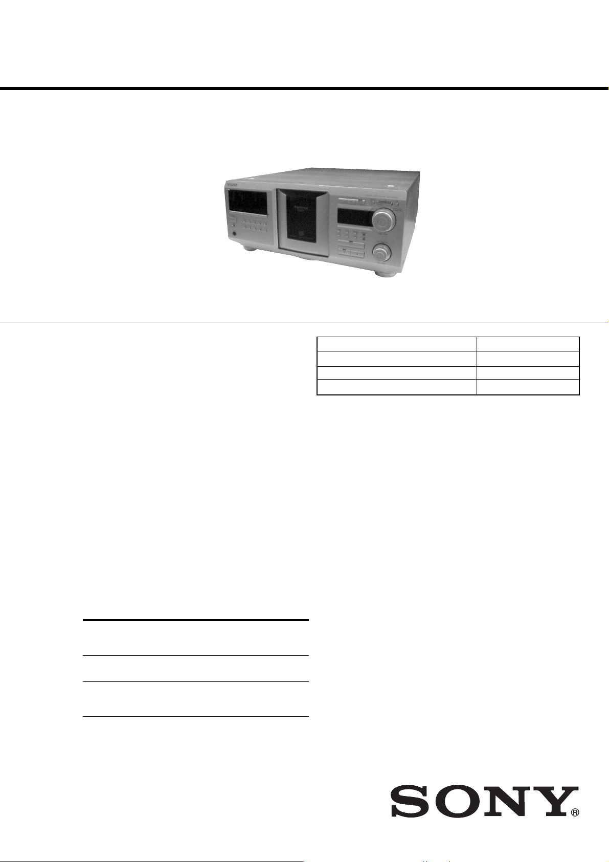
CDP-CX555G
• Audio cord (1)
• Monaural (2P) mini-plug cord (1)
• Remote commander (remote) (1)
• Size AA (LR6) batteries (2)
Compact disc player
Laser Semiconductor laser (λ = 780 nm)
Emission duration: continuous
Laser output Max 44.6 µW*
* This output is the value measured at
a distance of 200 mm from the
objective lens surface on the Optical
Pick-up block with 7 mm aperture.
Frequency response 20 Hz to 20 kHz ±0.5 dB
Signal-to-noise ratio More than 108 dB
Dynamic range More than 87 dB
Harmonic distortion Less than 0.009%
Output
LINE OUT
DIGITAL OUT
(OPTICAL)
Jack
type
Phono
jacks
Optical
output
connector
Maximum
output
level
2 V
(at 50 kilohms)
–18 dBm
Load
impedance
Over 10 kilohms
Wave length: 660 nm
General
Power requirements
Power consumption 16 W
1 W (at the Power Saving Mode)
Dimensions (approx.) 430 × 189 537 mm
(w/h/d) (17 7 1/2 21 1/4 in.) incl. projecting
parts
Mass (approx.) 8.8 kg (19 lbs 7 oz.)
Supplied accessories
Design and specifications are subject to change without notice.
100 V AC, 60 Hz
×
××
SERVICE MANUAL
Ver 1.0 2002. 10
Model Name Using Similar Mechanism NEW
CD Mechanism Type CDM62-K1BD46A
Base Unit Type BU-K1BD46A
Optical Pick-up Type KSM-213BFN
SPECIFICATIONS
Taiwan Model
9-874-178-01
2002J1600-1
© 2002.10
Sony Corporation
Home Audio Company
Published by Sony Engineering Corporation
COMPACT DISC PLAYER
Page 2
CDP-CX555G
Laser component in this product is capable of emitting radiation
exceeding the limit for Class 1.
This appliance is classified as
a CLASS 1 LASER product.
The CLASS 1 LASER
PRODUCT MARKING is
located on the rear exterior.
The following
caution label is
located inside of
the unit.
CAUTION
Use of controls or adjustments or performance of procedures
other than those specified herein may result in hazardous
radiation exposure.
Notes on chip component replacement
•Never reuse a disconnected chip component.
• Notice that the minus side of a tantalum capacitor may be
damaged by heat.
Flexible Circuit Board Repairing
•Keep the temperature of soldering iron around 270˚C
during repairing.
• Do not touch the soldering iron on the same conductor of the
circuit board (within 3 times).
• Be careful not to apply force on the conductor when soldering
or unsoldering.
SAFETY-RELATED COMPONENT WARNING !!
COMPONENTS IDENTIFIED BY MARK ! OR DOTTED LINE WITH
MARK ! ON THE SCHEMATIC DIAGRAMS AND IN THE PARTS
LIST ARE CRITICAL TO SAFE OPERATION. REPLACE THESE
COMPONENTS WITH SONY PARTS WHOSE PART NUMBERS
APPEAR AS SHOWN IN THIS MANUAL OR IN SUPPLEMENTS
PUBLISHED BY SONY.
2
Page 3

CDP-CX555G
SECTION 1
SERVICE NOTE
TABLE OF CONTENTS
1. SERVICE NOTE ·······························································3
2. GENERAL ··········································································6
3. DISASSEMBLY ································································7
3-1. Case ···············································································8
3-2. MAIN Board ································································· 8
3-3. TRANS Board ······························································· 9
3-4. Front Panel Assembly···················································· 9
3-5. JOG Board, DISP Board, KEYBOARD Board··········· 10
3-6. Cover (PT), Table (400) Assembly······························ 11
3-7. LED Board, Guide (Door)··········································· 11
3-8. DOOR SW Board························································ 12
3-9. Base (Door Driving) Assembly ···································13
3-10.Pop-up Assembly·························································13
3-11.D.MOTOR Board, Motor Assembly (Door) (M603) ··14
3-12.T.SENS Board, Holder (Table Sensor 400) ················· 14
3-13.D.SENS (OUT) Board, D.SENS (IN) Board ··············15
3-14.Back Panel Section······················································ 15
3-15.CD Mechanism, Magnet Assembly····························· 16
3-16.LOADING SW Board, LOCK SW Board ·················· 17
3-17.CDM Assembly ··························································· 18
3-18.Motor Assembly (Table) (M601),
Motor Assembly (Loading) (M602)···························· 18
3-19.BU Holder ···································································19
3-20.BD Board, Optical Pick-up (KSM-213BFN) ·············· 19
NOTES ON HANDLING THE OPTICAL PICK-UP BLOCK
OR BASE UNIT
The laser diode in the optical pick-up block may suffer electrostatic
break-down because of the potential difference generated by the
charged electrostatic load, etc. on clothing and the human body.
During repair, pay attention to electrostatic break-down and also
use the procedure in the printed matter which is included in the
repain parts.
The flexible board is easily damaged and should be handled with
care.
NOTES ON LASER DIODE EMISSION CHECK
The laser beam on this model is concentrated so as to be focused on
the disc reflective surface by the objective lens in the optical pickup block. Therefore, when checking the laser diode emission,
observe from more than 30 cm away from the objective lens.
The emission check enables continuous checking of the S curve.
LASER DIODE AND FOCUS SEARCH OPERATION
CHECK
Carry out the “S curve check” in “CD section adjustment” and check
that the S curve waveform is output three times.
4. TEST MODE···································································· 20
5. ADJUSTMENTS ···························································· 25
6. DIAGRAMS······································································29
6-1. Circuit Boards Location ··············································29
6-2. Block Diagrams··························································· 30
6-3. Printed Wiring Board – BD Board – ··························· 32
6-4. Schematic Diagram – BD Board – ······························ 33
6-5. Printed Wiring Board – MAIN Board – ······················34
6-6. Schematic Diagram – MAIN Board (1/2) – ················ 35
6-7. Schematic Diagram – MAIN Board (2/2) – ················ 36
6-8. Printed Wiring Board – Sensor Section –···················· 37
6-9. Schematic Diagram – Sensor Section – ······················ 37
6-10.Printed Wiring Board – Display Section – ··················38
6-11.Schematic Diagram – Display Section –····················· 39
6-12.Printed Wiring Board – JOG Board – ························· 40
6-13.Schematic Diagram – JOG Board – ····························41
6-14.Printed Wiring Board – Power Section – ···················· 42
6-15.Schematic Diagram – Power Section – ·······················43
6-16.IC Block Diagrams······················································ 44
6-17.IC Pin Function Descriptions ······································46
7. EXPLODED VIEWS ······················································50
7-1. Case Section ································································50
7-2. Chassis Section 1························································· 51
7-3. Chassis Section 2························································· 52
7-4. Front Panel Section ····················································· 53
7-5. Mechanism Section 1 (CDM62-K1BD46A)··············· 54
7-6. Mechanism Section 2 (CDM62-K1BD46A)··············· 55
7-7. Mechanism Section 3 (CDM62-K1BD46A)··············· 56
7-8. Mechanism Section 4 (CDM62-K1BD46A)··············· 57
7-9. Optical Pick-up Section (BU-K1BD46A)··················· 58
8. ELECTRICAL PARTS LIST······································· 59
3
Page 4
CDP-CX555G
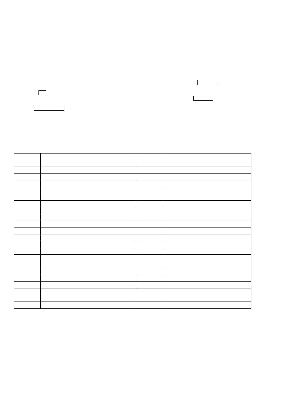
CD-TEXT TEST DISC
This unit is able to display the TEXT data (character information) written in the CD on its fluorescent indicator tube.
The CD-TEXT TEST DISC (TGCS-313:J-2501-126-A) is used for checking the display.
To check, perform the following procedure.
Checking Method:
1. Turn ON the power , set the disc on the disc ta ble with the side labeled as “test disc” as the right side, close the front cover , and chuck the
disc.
2. The following will be displayed on the fluorescent indicator tube. (The display switches each time the DISPLAY button is pressed.)
Display : CD TEXT Test Disc (Album Title)
3. Press the · button and play back the disc.
4. The following will be displayed on the fluorescent indicator tube. (If nothing is displayed, press the DISPLAY button.)
Display : 1kHz/0 dB/ L&R
5. Rotate l AMS L knob to switch the track. The text data of each track will be displayed.
For details of the displayed contents for each track, refer to “Table 1 : CD-TEXT TEST DISC Text Data Contents” and “Table 2 : CDTEXT TEST DISC Recorded Contents and Display”.
Restrictions in CD-TEXT Display
In this unit, some special characters will not be displayed properly . These will be displayed as a space or a character resembling it. For details,
refer to “Table 2 : CD-TEXT DISC Recorded Contents and Display”.
Table 1 : CD-TEXT TEST DISC Text Data Contents (TRACKS No. 1 to 41:Normal Characters)
TRACK
No.
1
2
3
4
5
6
7
8
9
10
11
12
13
14
15
16
17
18
19
20
21
Displayed Contents
1kHz/0dB/L&R
20Hz/0dB/L&R
40Hz/0dB/L&R
100Hz/0dB/L&R
200Hz/0dB/L&R
500Hz/0dB/L&R
1kHz/0dB/L&R
5kHz/0dB/L&R
7kHz/0dB/L&R
10kHz/0dB/L&R
16kHz/0dB/L&R
18kHz/0dB/L&R
20kHz/0dB/L&R
1kHz/0dB/L&R
1kHz/-1dB/L&R
1kHz/-3dB/L&R
1kHz/-6dB/L&R
1kHz/-10dB/L&R
1kHz/-20dB/L&R
1kHz/-60dB/L&R
1kHz/-80dB/L&R
TRACK
No.
22
23
24
25
26
27
28
29
30
31
32
33
34
35
36
37
38
39
40
41
Displayed Contents
1kHz/-90dB/L&R
Infinity Zero w/o emphasis//L&R
Infinity Zero with emphasis//L&R
400Hz+7kHz(4:1)/0dB/L&R
400Hz+7kHz(4:1)/-10dB/L&R
19kHz+20kHz(1:1)/0dB/L&R
19kHz+20kHz(1:1)/-10dB/L&R
100Hz/0dB/L*
1kHz/0dB/L*
10kHz/0dB/L*
20kHz/0dB/L*
100Hz/0dB/R*
1kHz/0dB/R*
10kHz/0dB/R*
20kHz/0dB/R*
100Hz Squere Wave//L&R
1kHz Squere Wave//L&R
1kHz w/emphasis/-0.37dB/L&R
5kHz w/emphasis/-4.53dB/L&R
16kHz w/emphasis/-9.04dB/L&R
NOTE : The contents of Track No. 1 to 41 are the same as those of the current TEST DISC-their titles are displayed.
4
Page 5
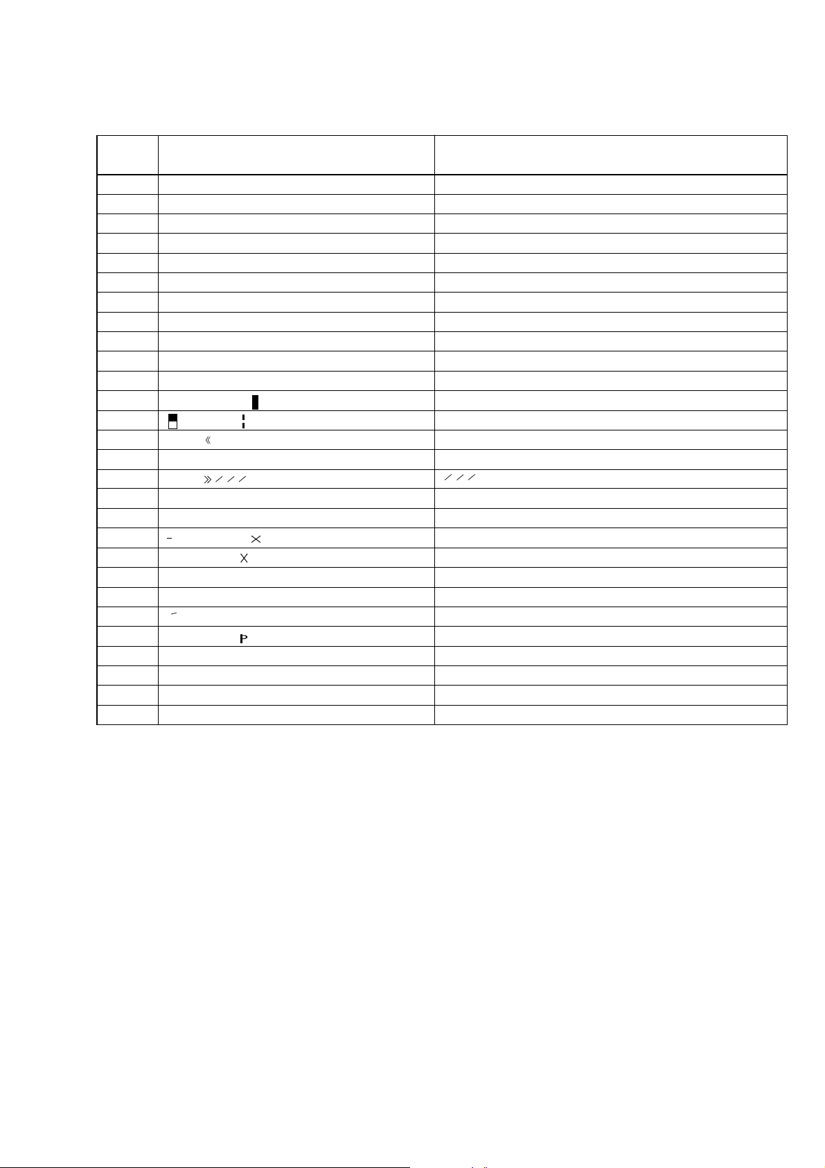
Table 2: CD-TEXT TEST DISC Recorded Contents and Display
(In this unit, some special characters cannot be displayed. This is no a fault.)
CDP-CX555G
TRACK
No.
42
43
44
45
46
47
48
49
50
51
52
53
54
55
56
57
58
59
60
61
62
63
64
65
66
67
to
99
Recorded contents Display
!”#$%& ´ (21h to 27h)1kHz 0dB L&R
( )+,–./ (28h to 2Fh)
*
01234567 (30h to 37h)
89:;<=>? (38h to 3Fh)
@A BCDEFG (40h to 47h)
HIJKLMNO (48h to 4Fh)
PQRSTUVW (50h to 57h)
XYZ[¥]^_ (58h to 5Fh)
abcdefg (60h to 67h)
′
hijklmno (68h to 6Fh)
pqrstuvw (70h to 77h)
xyz{I }
~
(78h to 7Fh)
i ¢£¤¥ § (A0h to A7h) 8859-1
¬
≥ C ª
•±23
1
º ¿ (B8h to BFh)
†
–
PR
µ ¶• (B0h to B7h)
′
14123
(A8h to AFh)
4
АБВГДЕЖЗ (C0h to C7h)
ИЙКЛМНОП (C8h to CFh)
DСТУФХЦ
Ø ÙÚÛÜY
˙
(D0h to D7h)
ß (D8h to DFh)
абвгдежз (E0h to E7h)
ийклмноп (E8h to EFh)
∂ стуфхц÷ (F0h to F7h)
ø ùúûüy
ÿ (F8h to FFh)
´
No.66
No.67
to
No.99
N All the same
N All the same
N All the same
N All the same
N All the same
N All the same
N All the same
XYZ[\]^_(58····
N All the same
N All the same
N All the same
N All the same
N All the same
N All the same
N All the same
14123
are displayed without “/”
4
N All the same
N All the same
N All the same
N All the same
N All the same
N All the same
N All the same
N All the same
N All the same
N All the same
to
N All the same
5
Page 6
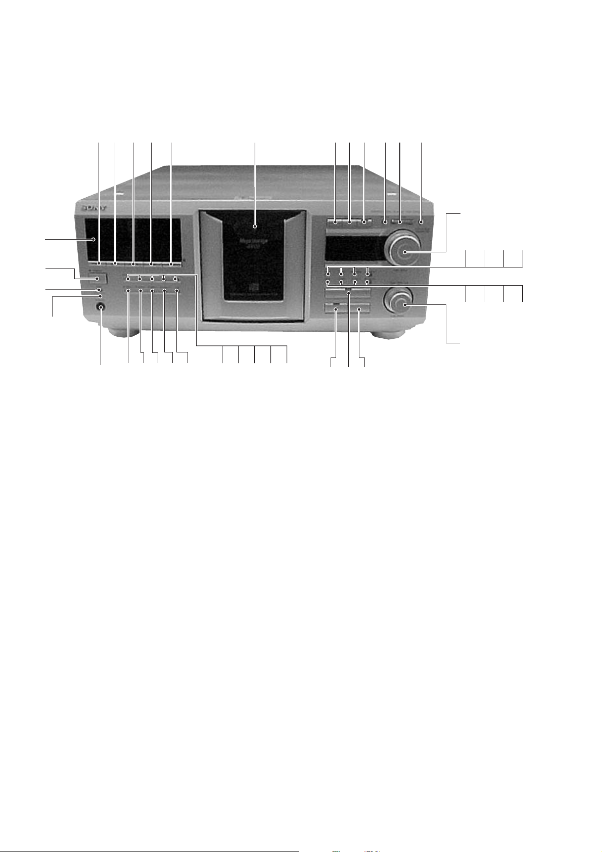
CDP-CX555G
Front Panel
SECTION 2
GENERAL
3
2
1
r;
4
el
765
9q;qaqsqdqfqg8
qh
qj w;qk ql
wa
wfws wd
wg
efejeheg
ed wles
ea e;ek
wk wj wh
LOCATION OF PARTS AND CONTROLS
1 1/u (power) button
2 STANDBY indicator
3 Display window
4 CONTINUE button
5 SHUFFLE button
6 PROGRAM button
7 REPEAT button
8 DISPLAY button
9 Front cover
q; OPEN/CLOSE button
qa DISC EJECT button
qs HISTORY button and indicator
qd MENU/NO button
qf +100 button
qg YES button
qh DISC/ALBUM/CHARACTER/PUSH ENTER knob and button
qj CHECK button
qk CLEAR button
ql NAME SEARCH button
w; ALBUM SELECT button and indicator
wa FADER button
ws X-FADE button
wd NO DELAY button
wf MEGA CONTROL button and indicator
wg l AMS L /PUSH ENTER knob and button
wh p (stop) button
wj · (play) button and indicator
wk P (pause) button and indicator
wl ARTIST MODE button and indicator
e; TOP ARTIST 4 button and indicator
ea TOP ARTIST 3 button and indicator
es TOP ARTIST 2 button and indicator
ed TOP ARTIST 1 button and indicator
ef TIME button
eg TOP ARTIST 8 button and indicator
eh TOP ARTIST 7 button and indicator
ej TOP ARTIST 6 button and indicator
ek TOP ARTIST 5 button and indicator
el KEYBOARD jack
r; TIMER OFF/PLAY switch
6
Page 7
SET
CASE
MAIN BOARD
CDP-CX555G
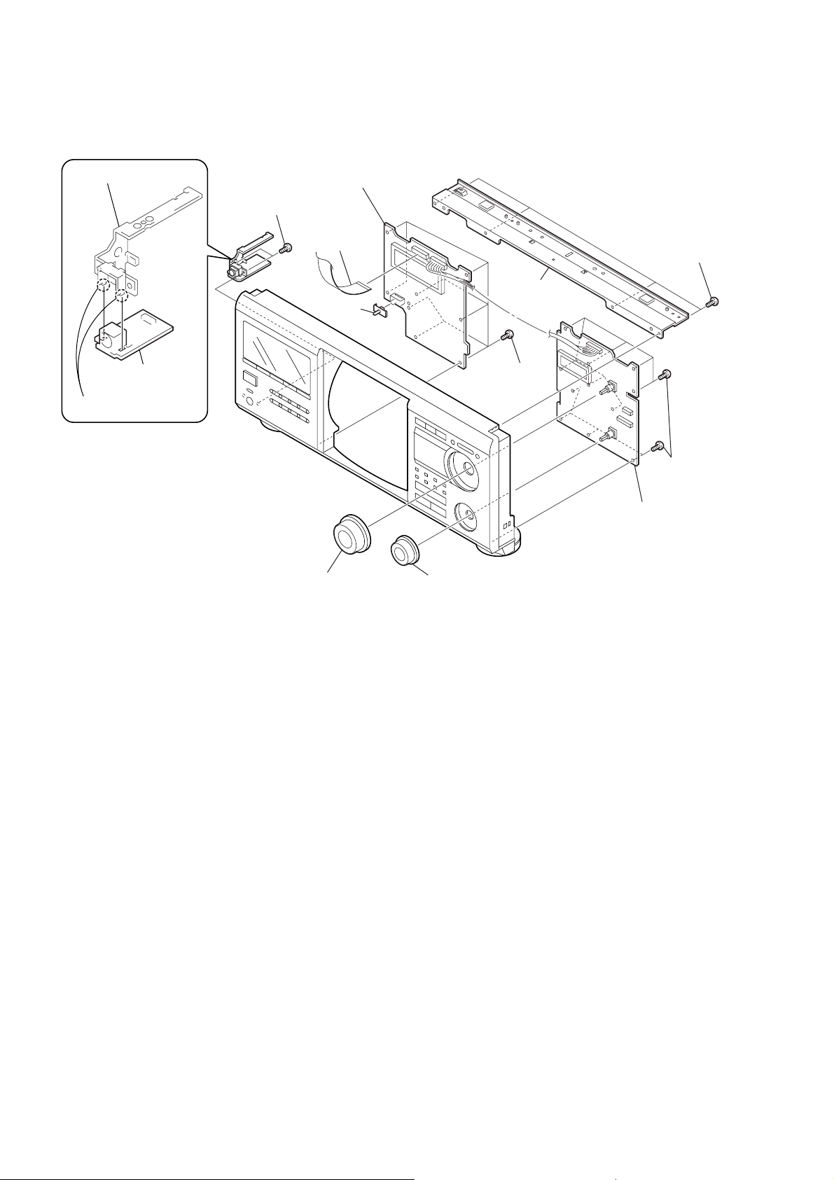
SECTION 3
DISASSEMBLY
FRONT PANEL ASSEMBLY
COVER (PT),
TABLE (400) ASSEMBLY
DOOR SW BOARD
BASE (DOOR DRIVING)
ASSEMBLY
TRANS BOARD
JOG BOARD,
DISP BOARD,
KEYBOARD BOARD
LED BOARD,
GUIDE (DOOR)
LOADING SW BOARD,
LOCK SW BOARD
T. SENS BOARD,
HOLDER
(TABLE SENSOR 400)
D. SENS (OUT) BOARD,
D. SENS (IN) BOARD
BACK PANEL SECTION
CD MECHANISM,
MAGNET ASSEMBLY
CDM ASSEMBLY
MOTOR ASSEMBLY
(TABLE) (M601),
MOTOR ASSEMBLY
(LOADING) (M602)
BU HOLDER
POP-UP ASSEMBLY
D. MOTOR BOARD,
MOTOR ASSEMBLY (DOOR)
(M603)
OPTICAL PICK-UP (KSM-213BFN)
BD BOARD,
7
Page 8
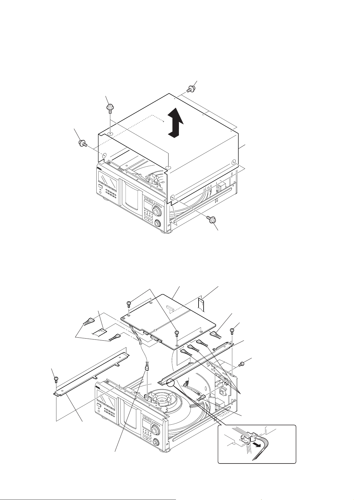
CDP-CX555G
e
)
Note : Follow the disassembly procedure in the numerical order given.
3-1. Case
2
two screws
(case 3 screw)
3
two screws
(case 3 screw)
1
three screws
(case 3 screw)
5
cas
3-2. MAIN Board
4
two connectors
(CN505, CN506)
qa
two screws
(BVTP 3 × 8)
5
flat type wire
(CN502)(17 core)
8
four screws
(BVTP 3 × 8)
0
MAIN board
4
two screws
(case 3 screw)
9
flat type wire
(CN501)(31 core)
2
connector (CN901)
qs
two screws (BVTP 3 × 8)
qg
bracket (R)
7
three screws
(BVTP 3 × 8)
1
three connectors
(CN503, CN801, CN903
3
connector (CNP902)
qf
bracket (L)
6
connector (CNP504)
qd
8
Page 9
3-3. TRANS Board
7
two screws
(PTTWH 3
A
2
connector
(CN602)
CDP-CX555G
5
screw (BVTP 3 × 8)
×
6)
A
6
bracket (PT)
3
connector (CN603)
8
TRANS board
3-4. Front Panel Assembly
3
4
screw
(BVTP 3 × 8)
connector (CNP503)
4
connector
(CN601)
7
2
Remove the claw.
1
connector
(CN991)
5
two screws
(BVTP 3 × 8)
1
6
three screws
(BVTP 3 × 8)
8
Remove the claw.
9
front panel assembly
9
Page 10
CDP-CX555G
s
3-5. JOG Board, DISP Board, KEYBOARD Board
qd
bracket (keyboard)
qf
KEYBOARD
board
qs
Remove two solderings.
qa
two screws
(BVTP 2.6 x 8)
8
DISP board
9
flat type wire
(17 core)
0
knob
(timer)
4
bracket (case)
assembly
7
eight screws
(BVTP 2.6 x 8)
3
four screws
(BVTP 2.6 x 8)
2
knob (disc)
1
knob (AMS)
6
JOG board
5
eleven screw
(BVTP 2.6 x 8)
10
Page 11
3
screw (BVTP 3 × 16)
4
guide (door)
5
table (400) assembly
6
washer
Note during re-assembling
When re-assembling, align
the positions as shown.
1
two screws
(BVTP 3
×
8)
2
cover (PT)
3-6. Cover (PT), Table (400) Assembly
CDP-CX555G
3-7. LED Board, Guide (Door)
2
LED board
1
screw (BVTP 3 x 8)
4
3
7
guide (door)
6
window (internal illumination)
5
11
Page 12
CDP-CX555G
3-8. DOOR SW Board
1
screw (PTPWH 2.6 × 8)
2
gear (cam)
3
screw (PTPWH 2.6 × 8)
4
gear (B)
5
two screws
(BVTP 2.6
6
DOOR SW board
×
8)
Precaution during the gear (cam) installation
1
Move the slider (pop-up) and the lever (pu joint) fully
in the direction of the arrow
slider (pop-up)
The levers of the two rotary switches on the D. SW board
are shown in the illustration below.
A
A
.
lever (pu joint)
two rotary switches
DOOR SW board
2
Install the gear (cam) in the direction shown
in the illustration and rotate it fully
in the direction of the arrow
3
When the gear (cam) happens to go too deep,
return it to the original position
in the direction of the arrow
B
C
.
.
gear (cam)
B
12
C
Page 13
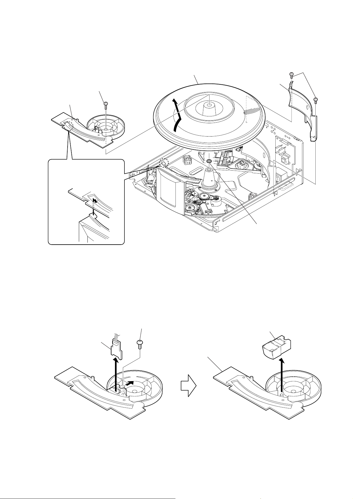
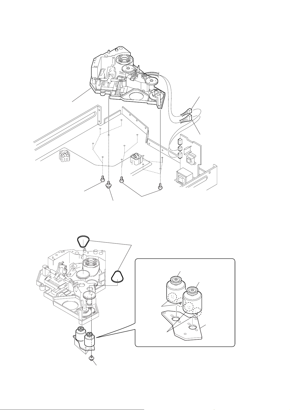
3-9. Base (Door Driving) Assembly
3
cover (table)
2
three screws (BVTP 3 × 8)
7
base (door driving)
assembly
CDP-CX555G
4
door assembly
3-10. Pop-up Assembly
5
two screws (BVTP 3 × 8)
2
step screw
3
pop-up assembly
1
connector
(CN602)
6
eight screws (BVTP 3 × 8)
1
screw (PTPWH 3 × 6)
13
Page 14
CDP-CX555G
d
3-11. D.MOTOR Board, Motor Assembly (Door) (M603)
1
belt
3-12. T.SENS Board, Holder (Table Sensor 400)
4
Remove two
solderings.
5
door motor assembly
3
2
two screws (BVTP 3 × 8)
(M603)
D.MOTOR boar
2
(CN83)
5
screw
(PTTWH 3
6
three claws
connector
×
6)
1
four screws
(PTPWH 3
4
T.SENS board
3
(CN81,CN82)
7
(table sensor 400)
×
6)
two connectors
holder
14
Page 15
3-13. D.SENS (OUT) Board, D.SENS (IN) Board
6
screw
1
screw
(PTTWH 3
4
screw
(PSW 3
×
8)
5
D.SENS (OUT) board
×
(PTTWH 3
6)
×
6)
7
D.SENS (IN) board
2
two step screws (T1)
3
bracket (sensor 400)
CDP-CX555G
3-14. Back Panel Section
4
bracket (CDM)
5
3
three screws
(BVTP 3
flat cable clamp
2
cover (CDM)
1
nine screws (BVTP 3 × 8)
×
8)
7
four screws
(BVTP 3
×
8)
8
back panel section
6
connector (CN991)
15
Page 16
CDP-CX555G
3-15. CD Mechanism, Magnet Assembly
1
three screws (BVTP 3 × 8)
3
bracket (top 400)
4
magnet assembly
5
washer
8
washer
2
three screws (BVTP 3 × 8)
7
CD mechanism
Note during re-assembling
When re-assembling,
align the positions as shown.
6
spring
16
Page 17
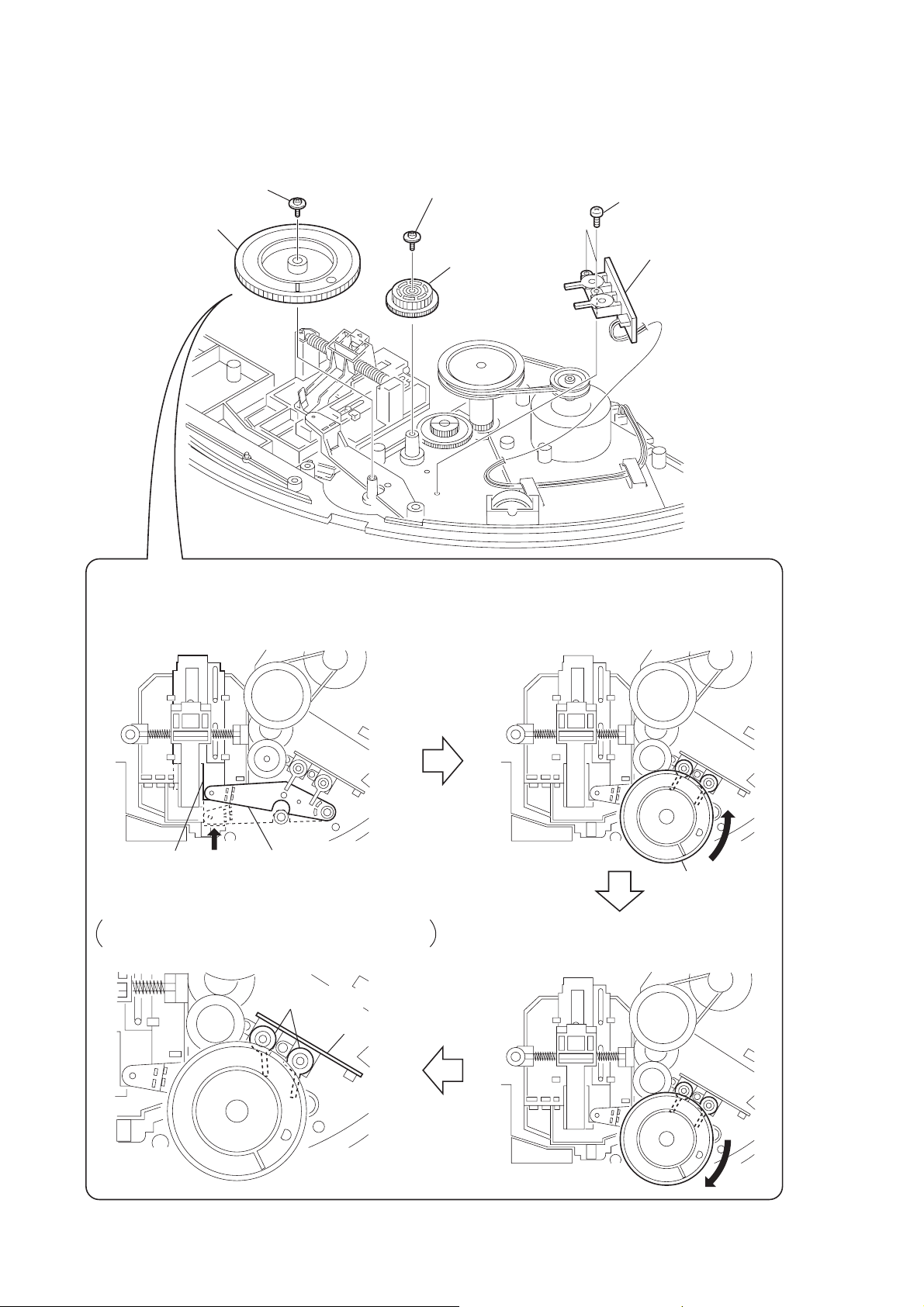
3-16. LOADING SW Board, LOCK SW Board
2
screw
(BVTP3 × 8)
A
B
1
Rotate the pulley (400) in the
direction of the arrow fully.
3
Rotate the pulley (400) in the
direction of the arrow fully.
A
B
CDP-CX555G
Note during re-assembling
When re-assembling the
LOADING SW board and
LOCK SW board,
align the leads position as shown.
LOADING SW board
LOCK SW board
Leads
position
claws
9
LOCK SW
board
8
screw
(BVTP 3 × 8)
7
gear (center)
5
tapping screw
4
belt
6
pulley (400)
0
screw
(BVTP 2.6 × 8)
qa
LOADING SW
board
17
Page 18
CDP-CX555G
)
3-17. CDM Assembly
6
CDM assembly
1
connector (CN603)
2
connector (CN601
4
four screws
×
(BVTP 3
8)
3
screw (PSW 3 × 8)
5
seven screws
(BVTP 3
×
8)
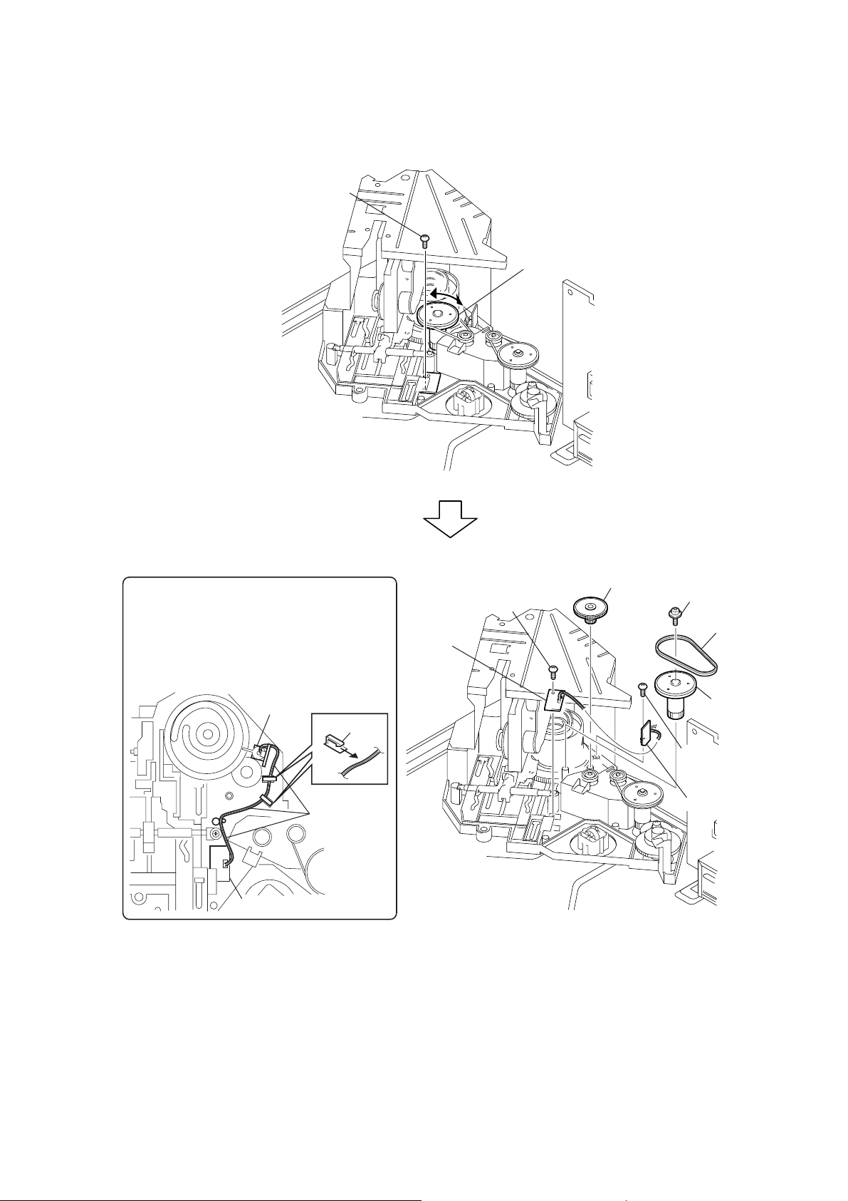
3-18. Motor Assembly (Table) (M601),Motor Assembly (Loading) (M602)
1
two belts
3
Remove two
solderings.
5
Remove two
solderings.
4
motor assembly (loading)
(M602)
6
motor assembly (table)
(M601)
7
board
L.T. MOTOR
18
2
three screws
(PTPWH 2.6
×
8)
Page 19
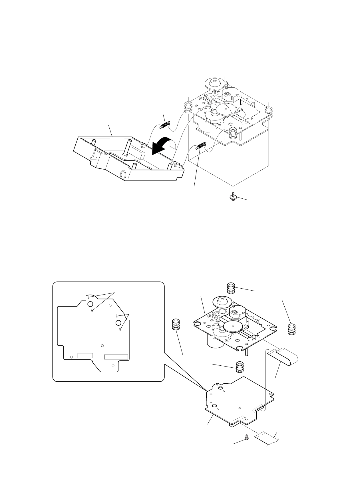
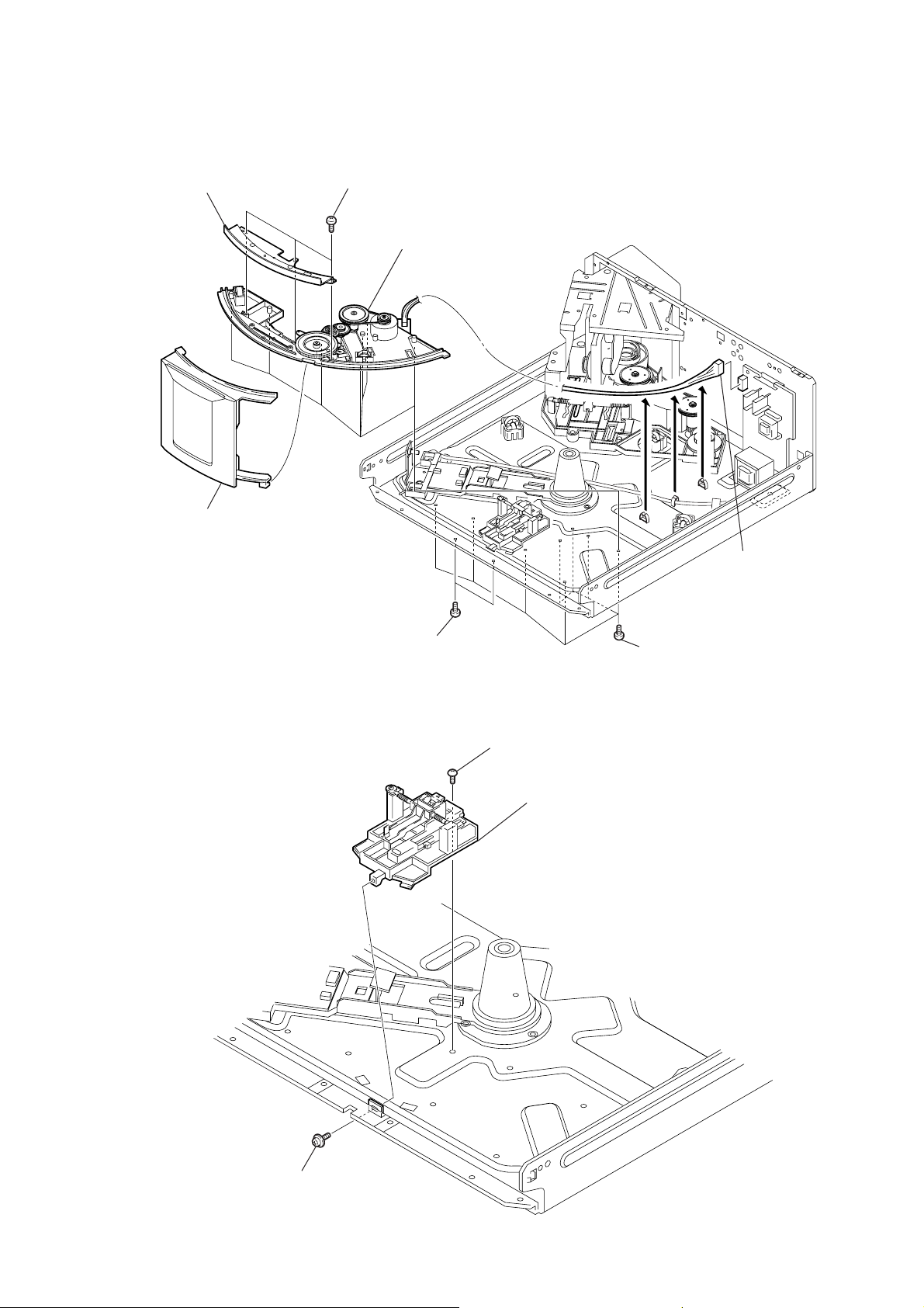
)
)
3-19. BU Holder
5
BU holder assy
3
tension spring (F-1)
CDP-CX555G
2
3-20. BD Board, Optical Pick-up (KSM-213BFN)
3
Remove two
solderings.
(spindle)
4
Remove two
solderings.
(sled)
4
tension spring (F-2)
9
optical pick-up
(KSM-213BFN)
1
four screws
(PTP WH 2.6 x 8
7
two vibration
proof rubbers
8
two vibration
proof rubbers
6
BD board
2
screw (+B 2 x 5)
5
wire (flat type)
(16 core) (CN102
1
wire (flat type)
(31 core)
(CN101)
19
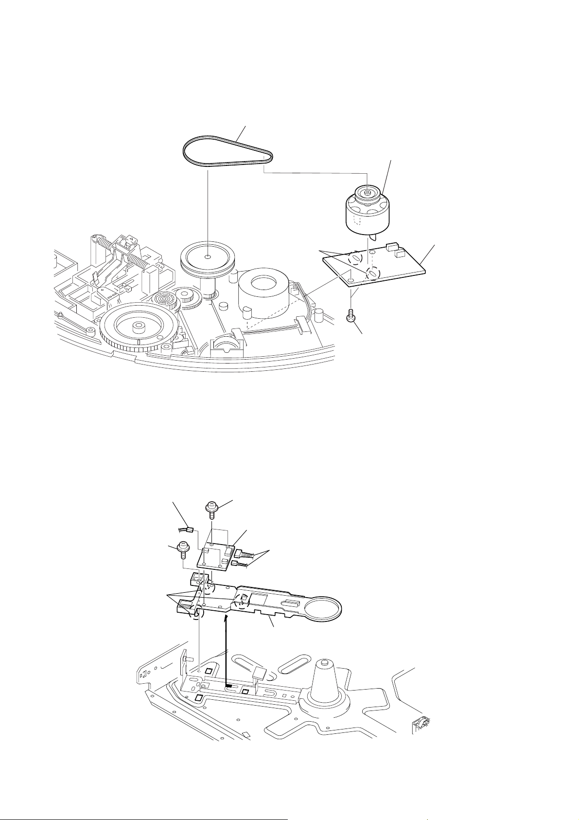
Page 20
CDP-CX555G
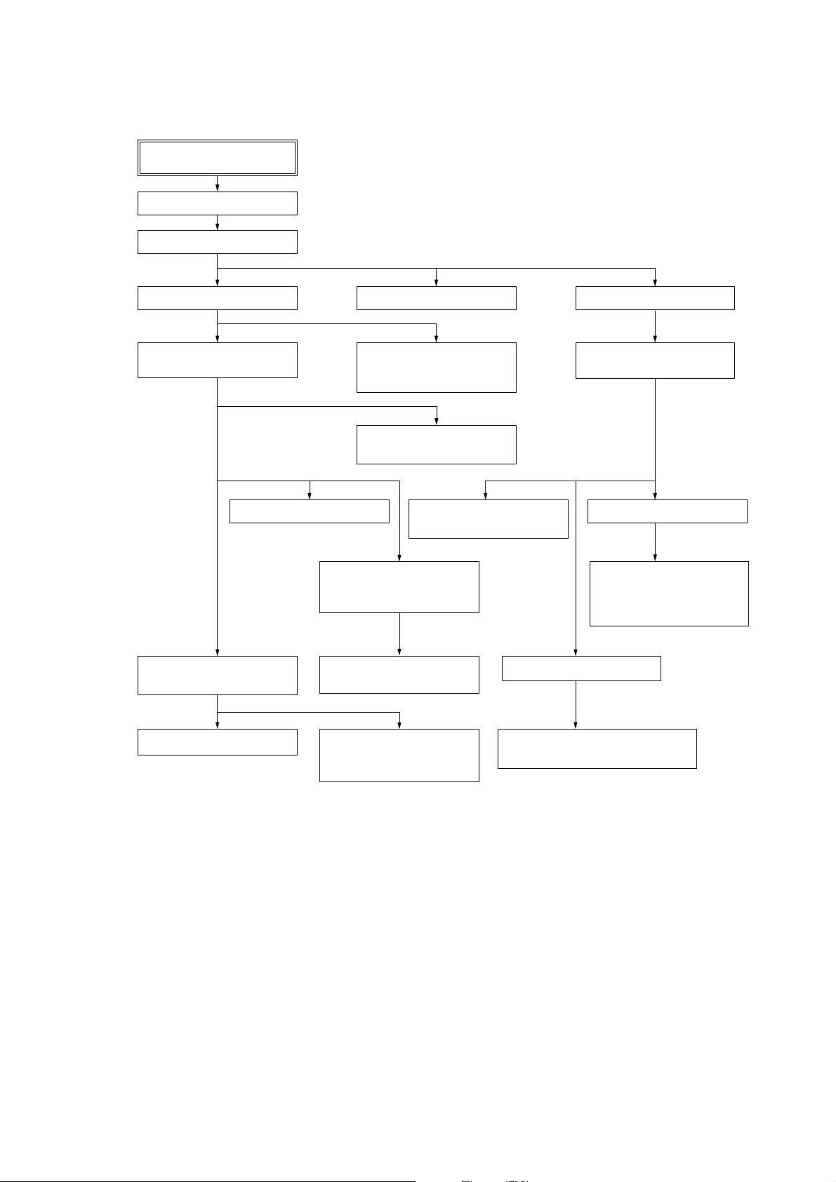
SECTION 4
TEST MODE
• This unit is provided with several test modes.
Details are shown in the following tables.
<Menu Method>
Turn on the power and press TIME , MEGA CONTROL and 1/u buttons.
Rotate the DISC/ALBUM/CHARACTER dial to select any of the following modes.
Push the DISC/ALBUM/CHARACTER dial to enter the test mode.
Display
Version
BU Test
CDM Test
Aging Mode
Ship Mode
To exit the mode, usually press the 1/u button to enter the standby state.
(When selecting the Ship mode, the standby mode is automatically entered.)
<3 Buttons Method>
Mode name
DOOR POP UP AGING MODE
ALL LIT MODE
MODEL NAME DISPLAY
SPRAY MODE
SHIPMENT MODE
To exit the mode, press the 1/u button to enter the standby state.
(When selecting the Ship mode, the standby mode is automatically entered.)
Software version display
BU test mode
CDM test mode
Normal aging mode
Default mode
Contents
Power supply state
ON
ON
ON
ON
ON
Mode name
TOP AR TIST 3 + H + +100
TOP AR TIST 4 + H + +100
TOP AR TIST 6 + H + +100
TOP AR TIST 8 + H + +100
ARTIST MODE + H + +100
Power supply state
Same as Ship Mode
20
Page 21
CDP-CX555G
SOFT WARE VERSION DISPLA Y
• Software version can be displayed on the fluorescent indicator tube.
Procedure:
With the power ON, while pressing the TIME and MEGA CONTROL
buttons, press the 1/u b utton.
Rotate the DISC/ALBUM/CHARACTER dial, select “Version”
and press the dial.
Software version is displayed on the fluorescent indicator tube.
To end this mode, press the 1/u button.
BU TEST MODE
• This mode is used for electrical adjustments.
Refer to the section on Electrical Adjustment.
CDM TEST MODE
•This mode is used for mechanical adjustments and electrical
adjustments.
Refer to the section on Mechanical adjustment and Electrical
Adjustment.
AGING MODE
• Mode which repeatedly changes and plays back discs automati-
cally in the unit.
• It will repeat aging as long as no errors occur.
• If an error occurs during aging, it will stop all servos, motors, etc.
instantaneously, display the error number, and stop operations.
The function serves to maintain the state of the unit when errors
occur.
Sequence of Aging Mode
$
1. Disc change
$
2. Load in
$
3. TOC read
$
4. Access of last track
$
5. 3 second playback
$
6. Access of first track
Order of Disc Change
(1 cycle takes 3 minutes)
$
1. No. 80
$
2. No. 320
$
3. No. 240
$
4. No. 400
$
5. No. 160
$
Special Aging Mode Functions
The aging mode is provided with the following convenient functions
1.Disc setting mode:
5 discs are set before setting the aging mode. This mode makes
the setting of these discs more easy.
2.Aging disc count function:
Functions which displays the number of aging discs carried out
on the Fluorescent indicator tube in numbers.
Aging Procedure
1. Turn on the power and press the TIME , MEGA CONTROL
and 1/u buttons.
2. Rotate DISC/ALBUM/CHARACTER dial, select “Aging
Mode” and press the dial to start the aging mode.
3. When the disc set mode is set, the · and P LEDs blink.
4. Rotate the DISC/ALBUM/CHARACTER dial. The slits (No.
80, 160, 240, 320, 400) for setting the discs will come forward.
Insert the discs into these slits. Do not set the discs in other
slits.
5. Press the · button.
6. The · LED blinks, the aging mode is set, and aging is started.
7. The aging cycle lasts 3 minutes. If errors occur during aging,
the error number will be displayed on the Fluorescent indicator
tube. (Refer to the following table for the details of the errors.)
8. Aging will be repeated as long as no errors occur.
9. After disc load out, the number displayed on the Fluorescent
indicator tube will increase.
10. To end aging, press the 1/u button .
If an error occurs and the 1/u button is useless, disconnect the
power cord from the outlet.
Display in aging cycle
AGED 10
DISC 180
$
7. 3 second playback
$
8. Load out
$
21
Page 22

CDP-CX555G
Error Display
1. Disc sensor error
120
1
PROGRAM 1 2 3 X-FADE DELETE
MULTI
Disc number
with error
Error code
Code number
2. Mechanism error
12 34 56 78
1
PROGRAM 1 2 3 X-FADE DELETE
CDTEXT
MULTI
Error code1
Error code2
Error code 1
Code number
0X
1X
2X
3X
4X
FX
X : negligible number
SECSTEPMINART.
CDTEXT
DISC
NO DELAY
HITART.NEXT2nd
REPEATSHUFFLE 1
CD2
GROUP
CD3
alternating
Y
GROUPTRACK
1234
Aging counter
Contents
No disc in the speified slit, or Disc in the
other slits
DISC
NO DELAY
HITART.NEXT2nd
REPEATSHUFFLE 1
CD2
CD3
GROUPTRACK
GROUP
Error code3
Y
alternating
SECSTEPMINART.
Error code4
1234
Aging counter
Contents
With no problem
With no problem
Error during door initialization
Error during loading initialization
Error during door initialization
With no problem
Error code 2
Code number
1X
2X
3X
4X
X : negligible number
Error code 3
Code number
1X
2X
X : negligible number
Error code 4
Code number
0X
1X
X : negligible number
3. BD error
DISC
12 34 56
1
PROGRAM 1 2 3 X-FADE DELETE
MULTI
CDTEXT
The state
during aging
Error code
Code number
01
02
03
04
05
06
Contents
Error during loading in
Error during loading out
With no problem
With no problem
Contents
Error during table operation
With no problem
Contents
With no problem
Error during table operation
SECSTEPMINART.
NO DELAY
HITART.NEXT2nd
REPEATSHUFFLE 1
CD2
GROUPTRACK
GROUP
CD3
alternating
Y
1234
Aging counter
Contents
From chucking to TOC read
From chucking to TOC read
From TOC read to end of last track playback
From TOC read to end of last track playback
From end of last track playback to end of first
track playback
From end of last track playback to end of first
track playback
22
Page 23

CDP-CX555G
SHIPMENT MODE
• This mode is used for setting the unit to the shipment state.
Do not execute it without a proper reason as it erases the
memory of the title memo recorded by the customer.
Procedure1:
With the power ON, while pressing the TIME button and MEGA
CONTROL button, press the 1/u button.
Rotate the DISC/ALBUM/CHARACTER dial, select “Ship Mode”
and press the dial. “-OFF-” is displayed and the standby mode is
automaticaly entered.
Procedure2:
With the power ON, while pressing the ARTIST MODE button
and H button, press the +100 button. “-OFF-” is displayed and
the standby mode is automatically entered.
DOOR POP UP AGING MODE
• This mode is used for performing aging of the CD pop up part
and door open/close.
It is used for checking if operations are performed normally.
Procedure1:
1. With the power ON, while pressing the TIME button and
MEGA CONTROL button, press the 1/u button.
2. Rotate the DISC/ALBUM/CHARACTER dial, select “CDM
Test”and press the dial.
3. Rotate the DISC/ALBUM/CHARACTER dial, select
“DoorPopup Aging” and press the dial.
4. Aging starts, and door open/close and up/down operations of
the pop up part are performed continuously.
5. To end this mode, press the 1/u button.
ALL LIT MODE
• This mode is used for lighting the whole fluorescent indicator
tubes and LEDs.
Procedure:
With the power ON, while pressing the TOP ARTIST4 and ·
buttons, press the +100 button.
Both the fluorescent indicator tubes and LEDs will light up
completely.
To end this mode, press the 1/u button.
MODEL NAME DISPLAY
• Model names can be displayed on the fluorescent indicator tube
for checking the microprocessor model setting, etc.
Procedure:
With the power ON, while pressing the TOP ARTIST6 and ·
buttons, press the +100 button.
The model name is displayed on the fluorescent indicator tube.
To end this mode, press the 1/u button.
SPRAY MODE
• This mode is used for the electrical adjustments.
Refer to the sedtion on Electrical Adjustment.
Procedure2:
1. With the power ON, while pressing the TOP ARTIST 3 b utton
and · button, press the +100 button.
2. Aging starts, and door open/close and up/down operations of
the pop up part are performed continuously.
3. To end the mode, press the 1/u button.
23
Page 24

CDP-CX555G
ADJ Mode
1. Turn ON the power of the unit, set disc to disc table, and perform
chucking.
2. Disconnect the power supply plug from the outlet.
3. To set ADJ mode, connect the test point (ADJ) of the MAIN
board to Ground, and connect the power supply plug to the
outlet.
In this mode, table rotation and loading operations are not performed
because it is taken that the disc has already been chucked.
Note: The same operations are also performed in the following when
the test point (ADJ) is connected to Ground after turning on
the power.
• Direct search (movement of sledding motor) is not performed dur-
ing accessing
• Ignored even when GFS becomes L
• Ignored even when the Q data cannot be read
•Focus gain does not decrease
To end the ADJ mode
1. Press the 1/u button and disconnect the plug.
2. Remove the wire between ADJ and GND.
Key and Display Check Mode
To set this mode, connect the test point (AFADJ) on the MAIN
board to Ground, and connect the power supply plug to the outlet.
Note:When this mode is executed, all title memos recorded will be
erased.
•When this button is pressed, “line # No. #” will be displayed.
However, these will not be displayed for the following special
buttons. However, these will not be displayed for the following
special buttons.
p (stop) button: FL segment check
(Refer to FL Tube Check Patterns)
P (pause) button: FL grid check
(Refer to FL Tube Check Patterns)
The P LED also lights up simultaneously.
· (play) button: All FL segment and grid will light up.
· LED also lights up simultaneously.
TIMER switch: When the switch position is PLAY , the
STANDBY LED lights up. It goes OFF
when set to OFF .
Each time this button is pressed, the value of the “Got ## keys”
increases. Buttons pressed once will not be counted when pressed
again.
FL Tube Check Patterns
Segment check
Grid check
Magnified
A B C D E F G
•When the jog dial and AMS is rotated to the right, the TOP AR T-
IST LEDs light up in the order of 1n 2..8n ARTIST
MODEnHISTORY ALBUM SELECTnMEGA CONTROL
n1.
•When the jog dial and AMS is rotated to the left, the TOP ART-
IST LEDs light up in the order of 8n7..1 nMEGA CONTR OL
ALBUM SELECTnHISTORYnARTIST MODEn8.
• Abbreviation
FL: Fluorescent Indicator Tube
To end the ADJ mode
1. Disconnect the plug.
2. Remove the wire between AFADJ and GND.
24
Adjustment Location: MAIN board (See page 28)
Page 25

SECTION 5
L
T
Holder (table sensor 400)
S tight, screw
(PTTWH 3
×
6)
Swing
Table (400) assembly
At this position,this
part will be locked.
ADJUSTMENTS
CDP-CX555G
Mechanical Adjustments
Pop Up Mechanism Adjustment
1. Turn on the power and set the disc to number 24.
2. With the power ON, while pres sing the TIME and MEGA
CONTROL buttons, press the
3. Rotate the JOG dial and select “CDM Test”.
Press the JOG dial.
4. Rotate the JOG dial and select the mechanism adjustment mode.
(“Mech Adjust” is displayed.)
Press the JOG dial.
5. Keep pressing the TOP AR TIST 1 button to operate the loading
mechanism, and continue pressing until the disc table locks.
(Fig. 1)
6. Keep pressing the TOP ARTIST 2 button to raise the pop up
part.
7. Loosen the adjusting screw , move the screwdri ver left and right
until the lever (POP UP) does not touch the slit wall, and secure
the screw. (Fig. 2)
The following buttons have special functions in this mode.
TOP ARTIST 1 button: Loading mechanism IN operation
TOP ARTIST 5 button: Loading mechanism OUT operation
TOP ARTIST 2 button: Pop up part UP operation
TOP ARTIST 6 button: Pop up part DOWN operation
button to enter the test mode.
1/u
Table Sensor Adjustment
1. Enter the CDM Test mode and select “Mech Adjust” with the
JOG dial, and press the dial.
2. Press the TOP ARTIST 1 b utton to operate the loading mechanism,
and continue pressing until the disc table locks. (Fig. 3)
3. Loosen the fixing screw and move the holder so that both PLAY
button LED (green) and the ALBUM SELECT button LED
(green) light.
If the holder is not in the correct position, the MEGA
CONTROL button LED (orange) or the PA USE b utton LED
(orange) lights.
4. Moving the disc table right and left with a hand after the screw
is fixed, the table will move by the play of a disc table. If the
LEDs light up alternately, the adjustment will be performed
correctly. (Fig. 4)
ALBUM SELEC
MEGA CONTRO
Cover (chassis 400)
Lever (POP-UP 400)
At this position,this
part will be locked.
Fig. 1
Fig. 3
Fix to the center so that the
lever (POP-UP 400) does
not touch the slit.
Fig. 2
Fig. 4
25
Page 26

CDP-CX555G
s
oscilloscope
BD board
TP (RFAC)
TP (DVC)
V
Electrical Adjustment
Note:
1. CD Block is basically designed to operate without adjustment.
Therefore, check each item in order given.
2. Use YEDS-18 disc (3-702-101-01) unless otherwise indicated.
3. Use an oscilloscope with more than 10MΩ impedance.
4. Clean the object lens by an applicator with neutral detergent
when the signal level is low than specified value with the
following checks.
S-Curve Check
oscilloscope
BD board
TP (FE1)
TP (DVC)
Procedure :
1. Chuck the disc (YEDS-18) beforehand.
2. Connect oscilloscope to test point TP (FE1) on BD board.
3. With the power ON, while pressing the TIME and MEGA
CONTROL buttons, press the 1/u button.
Rotate the DISC/ALBUM/CHARACTER dial, select “BU
Test” and press the dial.
4. Rotate the DISC/ALBUM/CHARACTER dial, and select “bdt
S CURVE”. Press the dial “LD AL” is displayed.
5. Check the oscilloscope waveform (S-curve) is symmetrical
between A and B. And confirm peak to peak level within 3±1
Vp-p.
RF Level Check
Procedure :
1. Connect oscilloscope to test point TP (RFAC) on BD board.
2. Turn Power switch on.
3. Put disc (YEDS-18) in to play the number five track.
4. Confirm that oscilloscope waveform is clear and check RF
signal level is correct or not.
Note: A clear RF signal waveform means that the shape “◊” can be
clearly distinguished at the center of the waveform.
RF signal waveform
VOLT/DIV : 500m
TIME/DIV : 1 µs
level : 1.2 Vp-p
+0.25
–0.20
Adjustment Location: BD board (See page 28)
S-curve waveform
symmetry
A
B
Within 3
VOLT/DIV : 1V
TIME/DIV : 400
±
1 Vp-p
µ
6. Pressing the MENE/NO button stops the output of the
waveform (S CURVE). “bdt S CURVE”is displayed.
7. To end this mode, press the ?/1 button.
Note : •Try to measure sev eral times to make sure than the ratio of
A : B or B : A is more than 10 : 7.
•Take sweep time as long as possible and light up the
brightness to obtain best waveform.
Adjustment Location: BD board (See page 28)
26
Page 27

CDP-CX555G
S
S
S
Disc Sensor Adjustment
Be sure to perform this adjustment after sensor adjustment in
MECHANICAL ADJUSTMENT .
Connection:
MAIN board
TP1
D.SENS OUT
GND
H-H OUT
D.SENS OUT: Pin
GND: Pin
H-H OUT: Pin
1
2
3
oscilloscope
CH1 CH2
Waveform:
CH1
CH2
D.SEN
H-H
1. Connect the oscilloscope to Pins 1, 2, and 3 of TP1 of the
MAIN board.
2. Check that no discs are loaded in the unit.
3.
With the power ON, while pressing the TIME and MEGA
CONTROL buttons, press the 1/u button. Rotate the DISC/
ALBUM/
CHARACTER dial, select “CDM Test” and press the
dial.
Rotate the DISC/
ALBUM/
CHARACTER dial and select
“TableRotation” and press the dial.
The disc table starts to rotate in the clockwise direction.
4. Loosen the fixing screw , move the mounting board (SENSOR),
and secure the mounting board (SENSOR) at the point the H
portion of the H-H waveform comes the center of the H portion
of the D.SENS waveform.
D. SENS (OUT) board
5. Rotate the DISC/ALBUM/CHARACTER knob in the
counterclockwise direction and the disc table starts to rotate in
the same direction. Check that the waveform at this time is the
same as that in step 4. If larger by a considerable extent, rotate
the DISC/ALBUM/CHARACTER knob in the clockwise
direction and the disc table starts to rotate in the same direction.
Repeat from step 4.
6. Rotate RV501 of the MAIN boar d and adjust so that the H and
L portions of the D.S waveform become the same.
CH1
Adjust so that these widths
become the same.
D.SEN
Adjustment Location: MAIN board (See page 28)
Spray Mode
• This mode is used for the measurement of the table sensor signal
outputs characteristics.
Procedure :
1. Check that no discs are loaded in the unit.
With the power ON, while pressing the TOP ARTIAT 8 and
H buttons, press the +100 button.
“Spray Mode” is displayed.
2. Press the H button to start the measurement. “Now ···ing” is
displayed during the measurement of one rotarion.
3. The result of the measurement is displayed as below.
display
DISC
P=3.6V b=1.4V
1
PROGRAM 1 2 3 X-FADE DELETE
NO DELAY
MULTI
CDTEXT
Minimum value
of the peak at the
High/High part of
TSENS1/TSENS2
HITART.NEXT2nd
REPEATSHUFFLE 1
CD2
GROUPTRACK
GROUP
CD3
Maximum value
of the bottom at the
LOW/LOW part of
TSENS1/TSENS2
SECSTEPMINART.
CH1
CH2
s tight, screw
(PTTWH 3
×
6)
Should be at the center
4. To end this mode, press the
D.SEN
1/u button.
H-H
27
Page 28

CDP-CX555G
Adjustment Location :
[ BD BOARD ] – Conductor Side –
IC 101
TP(RF AC)
TP(DVC)
TP(FE1)
[ MAIN BOARD ] – Component Side –
RV501
DISC SENSOR
ADJUSTMENT
IC 103
– Conductor Side –
GND
TP(AFADJ)
28
TP(ADJ)
IC504
IC501
TP1
13
Page 29

d
d
SECTION 6
LED board
MAIN board
TRANS board
D. MOTOR board
JOG board
BD board
DOOR SW board
T. SENS board
KEYBOARD board
D. SENS
(OUT) board
DISP board
D. SENS (IN) board
LOADING SW board
L. T. MOTOR board
LOCK SW board
DIAGRAMS
CDP-CX555G
THIS NOTE IS COMMON FOR PRINTED WIRING
BOARDS AND SCHEMATIC DIAGRAMS.
(In addition to this, the necessary note is printed
in each block.)
For schematic diagrams.
Note:
• All capacitors are in µF unless otherwise noted. pF: µµF
50 WV or less are not indicated except for electrolytics
and tantalums.
• All resistors are in Ω and 1/
specified.
¢
•
• C : panel designation.
Note: The components identified by mark 0 or dotted line
• A : B+ Line.
• B : B– Line.
• H : adjustment for repair.
•Voltages and waveforms are dc with respect to ground
•Voltages are taken with a V OM (Input impedance 10 MΩ).
•Waveforms are taken with a oscilloscope.
• Circled numbers refer to waveforms.
• Signal path.
: internal component.Note:
with mark 0 are critical for safety.
Replace only with part number specified.
under no-signal (detuned) conditions.
no mark : STOP
Voltage variations may be noted due to normal production tolerances.
Voltage variations may be noted due to normal production tolerances.
J : CD
c : digital out
4
W or less unless otherwise
For printed wiring boards.
Note:
• X : parts extracted from the component side.
• Y : parts extracted from the conductor side.
®
•
• : Pattern from the side which enables seeing.
(The other layers' patterns are not indicated.)
Caution:
Pattern face side: Parts on the pattern face side seen from the
(Side B) pattern face are indicated.
Parts face side: Parts on the parts face side seen from the
(Side A) parts face are indicated.
: Through hole.
• Indication of transistor
C
Q
EB
These are omitte
Waveforms
1
IC104 yd XO
59ns
1V/DIV, 20ns/DIV
2
IC103 qg (RFAC)
(PLAY)
500mV/DIV, 1µs/DIV
3
IC101 ra TE
APPROX 500mVp-p (PLAY)
200mV/DIV, 20ms/DIV
4
IC101 el FE
APPROX 500m Vp-p (PLAY)
200mV/DIV, 4ms/DIV
5
IC101 wg MDP
7.5 µs
1V/DIV, 4µs/DIV
6
IC501 ek X2
62.5 ns
1V/DIV, 20ns/DIV
6-1. Circuit Boards Location
3.8Vp-p
1.3Vp-p
1.65V
1.65V
2.1 Vp-p
3.5 Vp-p
C
EB
These are omitte
2929
Page 30

CDP-CX555G
6-2. Block Diagrams – BD Section –
OPTICAL PICK-UP
BLOCK
(KSM-213BFN)
VC
A
B
C
D
E
F
LD
GND
PD
VR
F+
FOCUS
COIL
TRACKING
COIL
• R-CH is omitted due to same as L-CH
• Signal Path
F-
T+
T-
+5V
: CD
: DIGITAL OUT
Q101
LD
DRIVE
(SLED)
(SPINDLE)
IC101
IC103
RF AMP
RF AC
VC
27
A
6
B
7
C
8
D
9
E
10
F
11
LD
1
PD
2
IC150
MOTOR/COIL DRIVE
CH1RO
18
CH1FO
17
CH2FO
12
CH2RO
11
CH3FO
14
RFDCO
RFDCI
FEI
SW
CH1RI
CH1FI
CH2FI
CH2RI
CH3FI
15
28
29
FE
16
17
TE
18
12
22
23
6
7
4
M
13
16
CH3RO
CH4RO
CH3RI
CH4INS
5
2
M
CH4FO
15
MUTE
20
DIGITAL SERVO
DIGITAL SIGNAL PROC.
RFAC
50
RFDC
43
FE
39
TE
41
SE
40
FFDR
33
FRDR
34
TFDR
31
TRDR
32
SFDR
29
SRDR
30
MDP
25
D OUT
PCMD
BCLK
LRCK
XTAI
XTAO
DATA
CLOK
XLAT
SQCK
SCLK
SCOR
SQSO
SENS
SSTP
XRST
+3.3V
IC901
+3.3V
OPTICAL
OUT
12
13
14
60
62
63
S101
(LIMIT IN)
+5V
64
66
67
65
71
72
X201
16.9MHz
4
6
5
77
8
15
76
7
26
2
IC121
+3.3V
4
REG
1
+2.5V
5+2.5V
REG
DIGITAL
OPTICAL
OUT
IC104
D/A CONV,
MP3 DECODER
SDIO
BCKIA
LRCKIA
CKO
XI
XO
MP3REQ
LO
RO
PO5
SDA
SCL
RESET
23
36PO4
26
37
5
6
43A MUTE
1
39
LOUT
LMUTE
R-CH
R-CH
IC105
89
10 11
43
Q501,502
MUTE CONT
65
12 13
21
Q327
IC401
LPF
31
IC501 (1/2)
SYSTEM CONTROL
SDA
97
SCL
99
A MUTE
18
MP3RST
7
MP3REQ
96
DATA
4
CLK
5
XLT
20
SQCK
17
SCOR
95
SUBQ
15
SENS
6
46
19
12
11
98
DOOROUT
XRST
PWM3
PWM2
PWM1
RF SW
IC302
AMP
21
SMUTE
29
DOORSW
DOORIN
TBLL
TBLR
TSENS1
TSENS2
TSENS3
TSENS4
DSENS
78
79LDSW
25LDIN
24LDOUT
27
26
23
22
87
91
88
92
86
IC302
AMP
67
Q321,325,326,
328,329
MUTE CONT
+5V
+5V
RV501
DISC
SENSOR
Q552
Q562
IC81-84
TABLE
SENSOR
Q81,D81
SENSOR
Q322
MUTE
Q941,942
MOTOR
SWITCH
Q951,952
MOTOR
SWITCH
DISC
Q324
MUTE
Q323
MUTE
6
7
4
3
4
6
DOWN
OPEN
CLOSE
(LOADING)
S622
(LOCK)
IC961
MOTOR
DRIVE
IC941
MOTOR
DRIVE
UP
S621
J903
S612
(POP UP)
S611
(DOOR)
8
2
2
8
M
M
M
2ND
CD IN
ANALOG
OUT
M602
(LOADING)
M603
(DOOR)
M601
(TABLE)
3030
Page 31

– Main Section –
IC504
SRAM
11
D801
(INSIDE)
D710
STANDBY
13
.
15
19
D0
D7
J821
BOARD
CONTROL
3
RECEIVER
+5V
A0
A14
WE
KEY
IC703+5V
REMOTE
CDP-CX555G
IC501 (2/2)
SYSTEM CONTROL
50
D0
57
D7
FLDATA
1
FLCLK
10
3
.
25
23
.
21
.
2
.
26
.
1
Q551
CE
20
27
X501
16MHz
Q571
Q570
1
Q572
LED
DRIVE
Q576
LED
DRIVE
66
73
.
63
60
.
65
.
49
.
64
47
48
39
38
89
85
45
93
13
31
30
A0
A14
CE
WE
X1
X2
KBDO
KBDI
KBCO
KBCI
RMIN
LED
SB_LED
FLT1
LEDLAT
FLRST
FLDATAI
TJOG1
TJOG2
KEY0
POWER
44
100
43FLT2
84DJOG1
81DJOG2
83
82
80
90
34RESET
94ACIN
2
3
8
RE701
AMS
RE702
DISC/
CHARACTER
S761-768
FUNCTION
KEY
63
DA
62
SCK
61
CS
60
RESET
4
DATA
8
CLK
7
RST
6
LT
IC701
FL DRIVER
DIG1
DIG15
DIG16
SEG01
SEG35
IC702
LED DRIVER
S701-706
FUNCTION
S711-714
FUNCTION
S721-726
FUNCTION
S741-745
FUNCTION
S751-755
FUNCTION
QC
QP
KEY
KEY
KEY
KEY
KEY
40
54
55
39
4AD1(36)
24
13,
11,
12
F1 F2
Q701
5
D701-709,711,
S714,S721
13
15
5
14
12
11
10
9
7
6
FLUORESCENT
INDICATOR TUBE
712,715
IC704
FL DRIVER
SEG0
SIN
SEG8
CLK
RESET
SEG9
SOUT
SEG14
CS
AD0
AD1
AD2
AD4
AD5
FL701
FL702
FLUORESCENT
INDICATOR TUBE
F1 F2
F1
F2
FL701
VFL
F1
F2
FL702
VFL
-20V REG
43
35
34
29
Q941, 942
Q951, 952
AU VCC
Q931
REG
AU VEE
(IC703, 501, 503) +5V
DVDD (+5V)
MUTE
+5V
+7V
+5V
M +B
M -B
D913
Q941
3
3
3
IC930
+5V
3
REG
IC931
+5V REG, RESET
5
VOUT
2
RST
IC910
IC920
IC921
VIN
+5V
REG
+7V
REG
+5V
REG
2
4
Q911
-30V REG
1
1
1
D911
RECT
D921-924
RECT
D931-934
RECT
D901-904
RECT
D905,906
RECT
T911
T901
L991
LINE
FILTER
AC
IN
ICSW
BUSIN
BUSOUT
Q901
28
16
14
Q950
J901
CONTROL A1 II
J902
RELAY
DRIVE
RY991
3131
Page 32

CDP-CX555G
6-3. Printed Wiring Board – BD Board –
12
A
B
• See page 29 for Circuit Boards Location.
34567891011
IC150
C
D
E
F
IC101
IC104
IC103
IC105
IC121
• Semiconductor
Location
Ref. No. Location
IC101 D-8
IC103 E-8
IC104 D-10
IC105 E-1
IC121 F-2
IC150 C-7
Q101 F-4
3232
Page 33

CDP-CX555G
6-4. Schematic Diagram – BD Board –
T
F
CN101
4
0
5
X
0
V
1
L
4
IC
7
C
T
R220
31P
F
.1
0
6
7
2
C
1k
• See page 29 for Waveforms. • See page 44, 45 for IC Block Diagrams.
• See page 46 for IC Pin Function Description.
C258
24p
CH
X201
16.9MHz
R253
1k
C259
0.1
F
FB102
C263
10
FB103
6.3V
FB104
0
F
p
0
0
k
0
0
2
1
2
1
1
7
7
2
2
R
C
C232
0.1
F
FB105
C266
0.1
F
IC121
BA33C25FP
FB101
C231
100
10V
C297
0.1
F
C208
C229
0.1
0.1
F
F
C207
0.1
F
C257
B
0.33
C254
22p
CH
R251
220
R252
1M
C269
6.3V
C253
0.1
F
C251
0.1 F
R265
220
2200p B
C260
220
4V
C201
220
4V
F
10
TC94A20F-CX4
47
4V
C267
k
p
0
0
0
2
1
2
4
0
5
7
2
2
R249
R
C
470
0
2
2
0
5
C256
2
0.1
R
F
IC104
C261C264
C252
0.1
47
F
4V
R266
220
C268
2200p
B
FB251
F
.1
0
5
5
2
C
FB292
0
C292
1
F
C250
0.1 F
FB291
0
C265
47
4V
0.1 F
C227
R230
220
470
R231
470
R232
470
R233
C203
1000p
R216
B
1M
R213
0
C206
47 4V
C202
0.1
F
C205
0.1
F
C230
0.1 F
C121
10
6.3V
C119
1
F
TP5
RFAC
C213
3300p
B
FB111
0
R102
R105
10k
1k
C104
C101
3300p
470p
B
CH
C102
R103
100k
0.1 B
C226
47
4V
7
0
M
2
1
R
k
.2
2
C209
6
100p
0
2
CH
R
k
1
8
0
1
4
2
1
R
2
R
0
5
0
B
1
0
C212
B
2
0
2200p
B
B
.1
0
1
1
2
k
C
1
5
0
2
R
1
C
7
4
.0
0
6
1
k
2
0
C
0
1
k
3
0
k
0
1
.2
2
2
2
R
0
4
2
0
R
2
R
IC101
CXD3068Q
R215
0
C224
k
0.1
3
3
F
1
0
2
R
S101
TP7
DVC
C223
C222
47
0.1
4V
F
k
1
9
1
2
R
TP6
RFDC
0
1
0
1
R
R104
10k
C103
E
E
470p
E
S
F
T
2
P
T
CH
4
3
P
P
T
T
R120
120k
C107
22p CH
C115
C117
0.1 F
100
10V
R117
100k
C116
0.1
B
R114
160k
R111
120k
R113
3.9k
8
k
1
0
1
1
R
C108
C111
0.1
F
R133
2.2k
R132
470k
R131
B
7
.4
0
3
3
1
C
100k
B
B
p
p
0
0
0
0
7
7
4
4
1
2
3
3
1
1
C
C
C158
R151
2200p
100k
B
220k
R152
R156
0
C152
0.1 F
C151
0.1
F
C150
100
10V
IC103
CXA2581N
47
4V
IC150
BA5947FP
C120
47
4V
C109
R126
12k
0.1
F
R125
12k
C110
0.1
B
R122
100k
R153
0
R155
TP8
MGND
TP10
VC
TP11
TP12
TP20
0
VCC
E
TP13
D
TP14
A
TP15
PD
C114
1000p B
Q101
2SB710
R124
10
C113
100
10V
R123
10
TP1
C118
CN102
1
16P
F
B
TP16
C
TP18
TP17
AGND
F
TP19
LD
TP9
IOP
TP21
TP22
TP23
TP24
TP25
TP26
TP27
TP28
3333
Page 34

CDP-CX555G
6-5. Printed Wiring Board – MAIN Board –
12
A
B
C
D
E
F
• See page 29 for Circuit Boards Location.
3456789
(Page 42)
IC921
IC920
IC402
IC901
IC302
IC910
IC401
(Page 42) (Page 42)
IC930
IC931
KEYBOARD
(Page 37) (Page 38)
(Page 40)
DISP
(Page 38)
(Page 40)
• Semiconductor
Location
Ref. No. Location
D327 D-4
D329 D-3
D501 G-4
D502 H-7
D551 G-8
D941 C-8
D942 C-8
IC302 F-3
IC401 E-4
IC402 E-3
IC501 G-6
IC504 G-7
IC901 F-2
IC910 B-4
IC920 C-3
IC921 B-3
IC930 B-4
IC931 B-5
Q321 D-5
Q322 E-3
Q323 E-2
Q324 D-2
Q325 D-3
Q326 E-5
Q327 D-4
Q328 D-3
Q329 D-3
Q421 D-5
Q422 E-2
Q423 E-2
Q424 D-2
Q425 D-3
Q426 D-5
Q501 F-5
Q502 F-5
Q551 G-7
Q552 B-6
Q562 B-6
Q570 B-7
Q571 B-7
Q572 H-6
Q576 H-7
Q941 C-8
Q950 B-2
G
H
(Page 32)
IC501
I
IC504
(Page 37)
3434
Page 35

CDP-CX555G
6-6. Schematic Diagram – MAIN Board (1/2) –
CN801
7P
DTC144-VSA-TP
• See page 29 for Waveforms. • See page 48 for IC Pin Function Description.
F
C550
1F
0.1
IC504
LC35256DM-70-TLM
Q551
5.5V
551
C
100
100
100
R552
R553
R554
8
9
0
7
k
k
k
0
11
1
0k
0k
2
k
k
10
T-7
10
51
0
5
133
D
55
S
551
R
R
1S
R522
100
0k
512
1
R
0
50
5
5
50
00
1
10
1
1
R
R
R5
R
R
1
CN505
9P
R504
2.2k
F
F
22
22
.0
.0
0
0
R503
08
1k
5
509
C
C
C510
C511
0.022
R502
0.022
10k
F
0k
1
R506
5
10k
F
50
R
F
.1
0
3
50
C
CN502
17P
C592
100
93
00
5
1
C
F
.1
0
04
5
C
10V
CN503
CN903
RV501
22k
R591
4.7k
6P
9P
C591
100
10V
Q502
BN1L3M-TP
SDA
TP501
R520
100
R546
100
R521
TP502
100
SCL
TP503
RFSW
R529
100k
Q501
BN1L4M-TP
C594
100
10V
R570
4.7k
BA1A4M-TP
1
57
R
4.7k
L502
Q570
Q571
BA1A4M-TP
JW
100
R535
100
R537
R519
100
100
R536
100
R538
F
k
00
00k
1
1
0.022
2
3
17
53
51
5
R
R
C
F
k
22
00
.7k
k
.0
1
1
4
1k
0
4
1
4
5
3
30
54
5
53
5
51
R
R
R
R
C
R515
4.7k
R514
10k
0
10
100
26
525
5
R
R545
100k
R
0
0
10
10
524
523
R
R
C505
0.1
F
C541
0.01
C542
4700p
00
1
C543
0.47
539
R
IC501
-CX4-3BA
0k
20k
10
2
2
41
5
54
R
R
0
100
10
540
527
R
R
100
28
5
R
D501
1SS133T-72
k
0
1
.2k
2
6
3
51
54
R
R
k
0
1
33
5
R
BN1A4M-TP
Q576
R501
100k
Q572
BA1A4M-TP
X501
16MHz
C519
1
50V
0k
1
C512
0.022
F
518
R
R517
D502
JW
1SS133T-72
TP1
(TEST)
CN504
2P
Q562
BN1L4M-TP
Q552
BN1L4M-TP
L501
C942
R942
2.2
R943
2.2k
C945
100
10V
470 16V
D941
RD6.2ES-T2B2
Q941
2SB734-T-3
C944
100
D942
35V
RD20ES-T2B2
C941
470 16V
4.7
R941
CN506
5P
C943
100
35V
R944
2.2k
3535
Page 36

CDP-CX555G
6-7. Schematic Diagram – MAIN Board (2/2) –
• See page 45 for IC Block Diagrams.
C518
0.1
F
D327
1SS133T-72
C514
0.1
C307
F
1
50V
C407
1
50V
C516
0.1 F
C321
4.7
50V
Q327
BN1L4M-TP
CN501
31P
C403
Q326
BN1L3M-TP
R321
100k
3300p
IC401(1/2)
BA4558
C303
3300p
BA1L4M-TP
R405
JW
R305
JW
IC401(2/2)
BA4558
Q421
C404
22
50V
R406
470k
R306
470k
C304
22
50V
Q426
BN1L3M-TP
R410
IC402(1/2)
BA4558
IC302(1/2)
BA4558
10k
C310
R310
Q425
BN1L4M-TP
0.1 F
10k
R407
2.7k
R409
4.7k
R309
4.7k
R307
2.7k
Q325
BN1L4M-TP
R421
100k
R412
10k
R411
10k
C411C410
0.1 F0.1 F
R311
10k
R425R325
100k100k
IC402(2/2)
BA4558
C311
0.1
F
R312
10k
Q328
BN1L4M-TP
R328
100k
IC302(2/2)
BA4558
D329
1SS133T-72
C405
470k
R313
470k
C305
22
50V
C329
4.7
50V
Q329
BN1L4M-TP
22
R414
50V
220
R422
2.2k
R413
Q422
2SC3622ATP-LK
R322
2.2k
R314
220
R329
100k
R424
2.2k
R415
220
Q423
2SC3622ATP-LK
R423
2.2k
Q323Q322
2SC3622ATP-LK2SC3622ATP-LK
R323
2.2k
R315
220
R324
2.2k
C401
22
50V
C301
22
50V
R327
100k
R403R402
3.3k3.3k
C402
1000p
R401
470k
C302
1000p
R301
470k
R303R302
3.3k3.3k
R426
100
R326
100
Q321
BA1L4M-TP
R417
4.7k
2SC3622ATP-LK
R440
220
R340
220
Q324
2SC3622ATP-LK
R317
4.7k
Q424
C427
22 25V
C428
470p
C328
470p
C327
22 25V
R439
470k
J903
R339
470k
L902
JW
L903
JW
R950
4.7k
C950
0.1
R951
L950
10k
GP1F32T
C954C953
0.1 F100 10V
Q950
2SC2603TP-EF
R952
10
C951
0.1
F
IC901
C952
0.1
J901
J902
F
C513
EB501
C502
C501
0.1
100
F
10V
0.1
F
470 10V
C927
IC910
C917
IC920
TA7807
470
10V
C928
470
10V
C935
100
10V
IC921
220k
R931
C913
1000
16V
L921
C923
1000
16V
IC931
BA3993
C936
3.3
50V
C938
470
10V
C914
1000 16V
C939
0.1
F
R932
2.2
C933
100
16V
C934
100
16V
IC930
NJU7201L50
-T3
CN901
CN902
9P
5P
3636
Page 37

CDP-CX555G
6-8. Printed Wiring Board – Sensor Section – 6-9. Schematic Diagram – Sensor Section –
• See page 29 for Circuit Boards Location.
IC84
H
TO
1-683-723-
MAIN BOARD
CN801
(Page 34)
12
12
IC83
IC82
IC81
D801
SELU5E23C
-TP15
(INSIDE)
R801
R81
820
CN81
7P
CT-L
R82
820
CNP504
47
C801
0.1 F
R83
820
RPI-1391
IC81
RPI-1391
IC82
RPI-1391
IC83
CN82
CT-L
R85
680
2P
CN83
CT-L
CNP82
2P WIRE
CNP83
2P
2P WIRE
(DISC SENSOR)
D81
GL528V
(DISC SENSOR)
Q81
PT483F1
CN504
(Page 34)
1-683-730-
12
12
R84
820
RPI-1391
IC84
12
1-683-724-
12
3737
Page 38

CDP-CX555G
6-10. Printed Wiring Board – Display Section –
12
A
IC703
B
C
• See page 29 for Circuit Boards Location.
34567891011
(Page 40) (Page 34)
63
KEYBOARD BOARD
B
TO
IC701
MAIN BOARD
CN503
(Page 34)
D
E
F
G
H
MODE
IC702
S768
TIMER
12
12
1
3
KEYBOARD
2
4
5
6
1-683-722-
12
12
• Semiconductor
Location
Ref. No. Location
D701 E-5
D702 E-4
D703 E-3
D704 E-2
D705 E-2
D706 F-5
D707 F-4
D708 F-3
D709 F-2
D710 E-7
IC701 C-3
IC702 D-2
IC703 A-1
Q701 D-3
3838
Page 39

CDP-CX555G
6-11. Schematic Diagram – Display Section –
• See page 44 for IC Block Diagrams.
FL701
C782
100
10V
R788 R789
100 100
IC703
NJL64H400A-1
IC702
IC701
PT6302-R-001
Q701
BA1A4M
3.3k
47p
R786
C788
C789
R787
100k
C792
0.001
S768
TIMER
R745
4.7k
J821
S766
S745
R765R766R767
4.7k10k22k
S765
S744
S764
R743R744
2.2k2.2k
S743
0.1
R784
100
C787
0.01
R763R764
2.2k2.2k
S763
R742
1k
S742
C784
100p
C785C786
100p100p
R762
1k
S762
S741
S761
M66310P-FP
100
R785
D701
TP15
SEL5821
R790
220
220p
C791
D702
TP15
SEL5821
D703
TP15
SEL5821
R782
100
R783
100
D704
TP15
SEL5821
D706
TP15
SEL5821
D707
D708
TP15
SEL5821
SEL5821
R791
220
5
709
D
TP1
TP15
C702
0.1
SEL5821
D705
R792
220
TP15
SEL5821
TP15
D710
EL5221
S
470
R793
CN701
9P
D823
RD5.1ES-T2B2
C821
0.1 F
CNP503
R755
4.7k
D822
C822
0.1
F
L821
L823
6P
RD5.1ES-T2B2
D821
RD5.1ES-T2B2
L824
L822
C823
10V
S755
S754
R753R754
2.2k2.2k
S753
R752
1k
S752
S751
CNP502
17P
C781
100
10V
100
781
R
3939
Page 40

CDP-CX555G
6-12. Printed Wiring Board – JOG Board –
A
B
C
• See page 29 for Circuit Boards Location.
12
345678
(Page 38)
DISC EJECT
IC704
D
E
F
G
E
(Page 34)
(Page 34)
H
12
12
4040
Page 41

CDP-CX555G
6-13. Schematic Diagram – JOG Board –
• See page 44 for IC Block Diagrams.
FL702
IC704
M35500BGP
C775
C773
0.1
C774
100
10V
5L
C776
0.1
22p
10k
R701
10k
R711
10k
R721
10k
R731
10k
R741
10k
R751
RE701
CNP701
9P
R775
100
D715 D711
SEL5521C
-TP15
R771 R772
100 150
SEL5521C
-TP15
D712
SEL5821A
-TP15
C778
R702
1k
0.022
C751
C777
100p
R794
100
0.1
0.022
C741
0.022
C731
0.022
C721
0.022
C711
0.022
C701
R774
100
R773
150
R722
S701
R712
1k
S711
1k
S721
S767
R703 R704
2.2k 2.2k
S702
R713 R714
2.2k 2.2k
S712
R723 R724
2.2k 2.2k
S722
S723
S713
S703
R725
4.7k
S724
S704
R726
10k
S725
S714
R705
4.7k
R706
S705
S726
S706
R707
22k
RE702
10k
R727
22k
CNP506 CNP505
5P 9P
4141
Page 42

CDP-CX555G
6-14. Printed Wiring Board – Power Section –
12
A
B
• See page 29 for Circuit Boards Location.
3456789
(Page 34)
CN902
IC941
IC961
CN903
(Page 34)
1-683-729-
12
12
1-683-728-
12
12
C
D
E
1-676-829-
CN901
(Page 34)
BOARD
1-683-726-
12
12
1-683-727-
12
1-683-725-
12
• Semiconductor
Location
Ref. No. Location
D901 B-2
D902 B-2
D903 B-2
D904 B-2
D905 B-2
D906 B-2
D907 B-1
D911 E-3
D912 E-4
D913 D-4
D921 D-3
D922 D-3
12
12
D923 E-3
D924 E-3
D931 D-3
D932 D-3
D933 D-3
D934 D-4
D935 C-3
D991 C-3
IC941 B-2
IC961 B-3
Q901 C-3
Q911 E-4
Q931 C-3
Q941 A-4
Q942 A-4
Q951 B-4
Q952 A-4
4242
Page 43

CDP-CX555G
6-15. Schematic Diagram – Power Section –
R623 R622
RF-500TB
(LOADING)
2.2k 1k
S622
CNP621
2P WIRE
CN621
2P WIRE
M601 M602
RF-500TB
(TABLE)
CNP601
4P WIRE
• See page 45 for IC Block Diagrams.
S621
S611 S612
CNP603
2P WIRE
CNP611
2P WIRE
2P WIRE
CN611
R612 R614
1k 2.2k
R613
CNP902
5P
Q901
2SC2603TP-
EF
T901
C991
0.01
250V
CN991
2P
C992
4700p
C993
L991
4700p
D991
F
RY991
1SS133T-72
D901
11EQS04-TA 2B
D902
D903
D907
1SS133T-72
C902
1
50V
11EQS04-TA 2B
11EQS04-TA 2B
D904
11EQS04-TA 2B
R902
10k
R903
2.2k
R901
1k
1SS133T-72
D906
1SS133T-72
R904
D905
10k
2.2k
M603
RF-500TB
CNP602
4P
WIRE
(DOOR)
CNP901
9P
C901
3300
16V
CN601 CN603
1
1
10
R976
R977
R978
C962
C972
0.1
0.1
10
R968
R975
1
R967
R965
1
R966
R914
100
CN602
15k
IC961
LA6510
15k
150k
R963
150k
R964
180k
R974
C963
R971
150k
C971
0.1
180k
R972
16k
R973
C973
0.1
0.1
R962
R961
150k
C961
0.1
16k
C942
R949
R948
2.2
50V
1
1
R947
R946
R945
100k
IC941
LA6510
0.47
C940
0.47
C941
4.7k
150k
R944
1k
R943
100k
R956
R940
R953
R954
100
100k
C943
R957
0.47
C951
R959
1
R958
1
4.7k
150k
BN1L4M-TP
1k
R955
100k
0.1
2.2k
R952
Q951
Q952
BA1L4M-TP
CNP903
9P
AMP-S(WIRE)
R942
D913
RD6.2ES-T2B2
R913
4.7k
Q931
Q941
Q942
BA1L4M-TP
R941
2SC2603TP-
100
EF
C933
47
50V
D935
RD15ES
-T2B2
R951
100
BN1L4M-TP
2.2k
C912
Q911
2SB734-T-3
4
100
35V
D912
C921
2200
16V
C922
2200
16V
R931R932
2.2k2.2k
R912
2.2k
RD30ES-T2B1
D923
D924
C931
2200
16V
C932
2200
16V
R911
4.7k
D922
11ES2-NTA2 B
11ES2-NTA2 B
D931
D932
10E2N-TA2B
D933
10E2N-TA2B
D934
10E2N-TA2B
C911
11ES2-NTA2B
100
63V
D921
11ES2-NTA2 B
11ES2-NTA2 B
10E2N-TA2B
D911
0.022
C920
0.022
C930
EB1
T911
4343
Page 44

CDP-CX555G
6-16. IC Block Diagrams
IC104 TC94A20F-CX4 (BD BOARD)
33
PO2
PO3
34
VDDT
35
PO4
36
37
PO5
38
PO6
39
MP3REQ
40
VSS
PO1
General
IC702 M66310FP (DISP BOARD)
QC
24
0
CK
PO0
DOUT
TESTP
DIT
Output Port
2sets
Address Calc.
ERAM
2k word
VRAR
VSSR
DAC DAC
Bus
Switch
register
C-Pointer
register
Y-Pointer
register
X-Pointer
RO
VDAR
2526272829303132 1718192021222324
VDAL
LO
VRAL
VSSL
VSS
STANDBY
VDD
LRCKIB
BCKIB
16
SDI1
15
LRCKIA
14
BCKIA
13
12
SDIO
11
LRCKO
ALU
AX AY
A2 A3
Audio I/F
10
BCKO
9
SDO
DR
1
CK
DR
D
CK
1
D
CK
00
1 2 3
QA
R
R
QD
23
0
CK
DR
1
CK
DR
R
D
CK
1
R
D
CK
QB
QE
22
0
CK
DR
1
CK
DR
VCC
QF
21
0
CK
DR
1
CK
DR
4 5 6 7 8 9 10 11 12
DATA
QG
20
0
CK
DR
1
CK
DR
OE
QH
19
0
CK
DR
1
CK
DR
LT
QI
18
0
CK
DR
1
CK
DR
RST
QJ
17
0
CK
DR
1
CK
DR
CLK
QK
16
0
CK
DR
1
CK
DR
GND
QL
15
0
CK
DR
1
CK
DR
SQP
R
R
QN
13
0
CK
DR
1
CK
DR
R
D
CK
1
R
D
CK
QP
QM
14
0
CK
DR
1
CK
DR
D
CK
1
D
CK
00
QO
IRQ
VDDM
AMUTE
FI1
VSSM
PI0
PI1
VSS
IC704 M35500BGP (JOG BOARD)
DIG8/SEG17
DIG9/SEG16
DIG10/SEG15
DIG11/SEG14
DIG12/SEG13
DIG13/SEG12
DIG14/SEG11
DIG15/SEG10
33
32 31 30 29 28 27 26 25 24 23
SEG7
SEG6
SEG5
SEG4
SEG3
SEG2
SEG1
SEG0
VDD
34
35
33
36
33
37
33
38
33
39
33
40
33
41
33
42
43
44
DIGITAL/SEGMENT
OUTPUT CIRCUIT
DISPLAY CONTROL
CIRCUIT
DISPLAY
SERIAL
A-D
CONVERTER
GENERATOR
RAM
I/O
TRIGGER
CLOCK
MODE
REGISTER
MEMORY
ADDRESS
TRANSFER
COUNTER
ANALYTIC CIRCUIT
SELECTOR/A-D
CONTROL CIRCUIT
DIG6
DIG7
DIGITAL
OUTPUT CIRCUIT
COMMAND
NOISE FILTER
NOISE FILTER
DIG5
22
DIG4
21
DIG3
DIG2
20
DIG1
19
18
DIG0
VEE
17
VEE
16
15
SCLK
14
SOUT
SIN
13
CS
12
MX MY MZ
PROM
VC0
5857555351
Program
1k *3
VCOI
Control
=12k word
MAC
VDDP
A0 A1
Timing
Generator
CKO
10bit
61 62 63 646059565250
round & limit round & limit
Decoder
Instruction
XI
VDDX
XO
Microcom. I/F
VSSX
8
7
6
5
4
3
2
1
VDDT
/WIACK
SCL
SDA
/MILP
/MICS
MIMD
/RESET
DIG16/SEG9
DIG17/SEG8
SubQ
I/F
Y-Bus
register
FI2/SBSY
Y0 • Y1 • Y2
XO • X1 • X2
PRAM
256 word
PDO
VSSP
41
42
43
44
45
46
47
48
Timer
Interrupt
DRAM I/F
49
PI2
Fiag
Control
I-Bus
General
Input Port
PI3
PI4/CLCK
*7
CROM
4k word
YRAM
4k word
XRAM
4k wors
SRAM I/F
VDD
PI5/DATA
X-Bus
1Mbit
SRAM
54
TSTIN/SFSY
21 3 4
VDD
XOUT
VSS
XIN
5
RESET
6 7 8 9 10 11
AN5
AN4
AN3
AN2
AN1
AN0
4444
Page 45

IC931 BA3993F (MAIN BOARD)
CDP-CX555G
POFF
TSD
Band Gap
1 2
GND
GND
78
GND
6
5
IC941, IC961 LA6510 (TRANS BOARD)
–
+
1 2 3 4 5 6 7 8 9 10
–VIN1
VOUT1
VSENCE1
3
4
CT
+VIN1
VEE
–
+
+VIN2
–VIN2
VOUT2
VCC
VSENCE2
IC103 CXA2581N-T4 (BD BOARD)
RW/ROM
DC OFST
30
RFDCI
29
–
+
RFDCO
28
VC
VC
27
DVC
A
–
+
B
C
DVC
D
–
VOFST
VC
+
RW/ROM
DVC
VCC
EQ IN
AC SUM
GND
DVCC
DVC
RFAC
LD
PD
A
B
C
D
E
F
SW
VC
1
2
APC AMP
EQ ON/OFF
3
A
A
B
C
D
APC-OFF
(Hi-Z)
RW/ROM
(H/L)
RFAC
SUMMING
AMP
BCD
GM
GM
B
D
A
C
4
5
6
7
8
9
10
11
12
13
DVC
14
15
RW/ROM
VOFST
B
–
C
+
A
D
RW/ROM
RW/ROM
–
+
RW/ROM
RW/ROM
VOFST
–
+
RW/ROM
EQ
RFAC
VCA
VCC
–
+
DVC
VC
VC
–
+
DVC
VC
RFC
26
VFC
25
BST
24
RFG
23
VCC
22
CEI
21
CE
20
TE BAL
19
18
TE
17
FEI
16
FE
45
Page 46

CDP-CX555G
6-17. IC Pin Function Descriptions
• IC104 TC94A20F-CX4 D/A Converter, MP3 Decoder (BD Board)
Pin No.
1
2
3
4
5
6
7
8
9
10
11
12
13
14
15
16
17
18
19
20
21
22
23
24
25
26
27
28
29
30
31 to 34
35
36
37
38
39
40
41
42
43
44
45
46, 47
48
49, 50
51
52
53
54
55
Pin Name
/RESET
MIMD
/MICS
/MILP
SDA
SCL
/MIACK
VDDT
SDO
BCKO
LRCKO
SDI0
BCKIA
LRCKIA
SDI1
BCKIB
LRCKIB
VDD
STANDBY
VSS
VSSL
VRAL
LO
VDAL
VDAR
RO
VRAR
VSSR
TESTP
DOUT
PO0 to PO3
VDDT
PO4
PO5
PO6
MP3REQ
VSS
IRQ
VDDM
AMUTE
FI1
VSSM
PI0, PI1
VSS
PI2, PI3
PI4/CLCK
VDD
PI5/DATA
TSTIN/SFSY
FI2/SBSY
I/O
I
Reset input terminal “L”: reset
I
Microcomputer interface mode selection input “H”: I2C, “L”: TSB (fixed at “H”)
I
Microcomputer interface chip select signal input (fixed at “L”)
I
Microcomputer interface latch pulse input (fixed at “L”)
I/O
Serial data input/output
I
Serial clock input
O
Microcomputer interface acknowledge signal output (open)
–
Power supply (3.3V) for digital circuit
O
Data output (open)
O
Bit output (open)
O
LR clock output (open)
I
Data input 0
I
Bit clock input A
I
LR clock input A
I
Data input 1 (fixed at “L”)
I
Bit clock input B (fixed at “L”)
I
LR clock input B (fixed at “L”)
–
Power supply (2.5V) for digital circuit
I
Standby mode control signal input “H”: STB, “L”: normal (fixed at “L”)
–
Ground for digital circuit
–
Ground for DAC Lch
–
Reference voltage terminal for DAC Lch
O
DAC Lch signal output
–
Power supply (2.5V) for DAC Lch
–
Power supply (2.5V) for DAC Rch
O
DAC Rch signal output
–
Reference voltage terminal for DAC Rch
–
Ground for DAC Rch
I
Terminal for test “H”: test mode, “L”: normal (fixed at “L”)
O
SPDIF signal output (open)
O
General purpose output (open)
–
Power supply (3.3V) for digital circuit
O
General purpose output (LMUTE signal output)
O
General purpose output (RMUTE signal output)
O
General purpose output (open)
O
Interrupt request signal output to the system control (IC501)
–
Ground for digital circuit
I
External interrupt signal input (open)
–
Power supply (2.5V) for the internal 1Mbit SRAM
I
Flag signal input 0 (AMUTE signal input)
I
Flag signal input 1 (fixed at “L”)
–
Ground for the internal 1Mbit SRAM
I
General purpose input (fixed at “L”)
–
Ground for digital circuit
I
General purpose input (fixed at “L”)
I
General purpose input/SUBQ interface clock input or output (fixed at “L”)
–
Power supply (2.5V) for digital circuit
I
General purpose input/SUBQ interface data input (fixed at “L”)
I
Terminal for test/SUBQ interface frame sync input (fixed at “L”)
I
Flag signal input 2/SUBQ interface block sync input (fixed at “L”)
Description
46
Page 47

CDP-CX555G
Pin No.
56
57
58
59
60
61
62
63
64
Pin Name
VSSP
PDO
VCOI
VDDP
CKO
VDDX
XI
XO
VSSX
I/O
–
Ground for VCO circuit
O
PLL phase error detection signal output
I
VCO control voltage input
–
Power supply (2.5V) for VCO circuit
O
External clock output
–
Power supply (2.5V) for oscillation circuit
I
Resonator terminal (input)
O
Resonator terminal (output)
–
Ground for oscillation circuit
Description
47
Page 48

CDP-CX555G
• IC501 µPD703033AYGF-CX4-3BA System Control (MAIN Board)
Pin No.
1
2
3
4
5
6
7
8
9
10
11
12
13
14
15
16
17
18
19
20
21
22
23
24
25
26
27
28
29
30
31
32
33
34
35
36
37
38
39
40
41
42
43
44
45
46
47
48
49
50
Pin Name
FLDATA
FLCLK
LEDLAT
DAT A
CLK
SENS
MP3RST
FLRST
EVDD
EVSS
PWM1
PWM2
RMIN
BUSOUT
SUBQ
BUSIN
SQCK
AMUTE
PWM3
XLT
IC/VPP
TBLR
TBLL
LDOUT
LODIN
DOORIN
DOOROUT
ICSW
SMUTE
SBLED
LED
DSENSOUT
H-HOUT
RESET
XT1
XT2
REGC
X2
X1
VSS
VDD
CLKOUT
FLT2
FLT1
KBCO
XRST
CE
WE
A4
D0
I/O
O
Data signal output to the fluorescent indicator drivers amd LED driver
O
Clock signal output to the fluorescent indicator drivers and LED driver
O
Latch signal output to the LED driver
O
Data output to the DSP
O
Clock signal output to the DSP
I
SENS signal input from the DSP
O
Reset signal output to the IC104
O
Reset signal output to the the fluorescent indicator driver amd LED driver
–
Power supply (I/O port)
–
Ground (I/O port)
O
PWM1 signal output
O
PWM2 signal output
I
Data input from the remote control receiver
O
CONTROL A1 signal output
I
CD SUBQ signal input from the DSP
I
CONTROL A1 signal input
O
CD SUBQ clock signal output to the DSP
O
Muting signal output to the IC104
O
PWM3 signal output
O
Latch signal output to the DSP
–
Connected to ground
O
Table motor control signal output (clockewise)
O
Table motor control signal output (counterclockewise)
O
Loading motor control signal output (out)
O
Loading motor control signal output (in)
O
Door motor control signal output (close)
O
Door motor control signal output (open)
O
Power supply to the peripheral ICs
O
2nd audio input muting signal output
O
Sandby LED control signal output
O
Inside illumination LED control signal output
O
Disc sensor readout result signal output
O
Or signal of TSENS1/TSENS2 output
I
System reset input
I
Sub clock input
O
Sub clock output
–
Capacitor connection terminal for regulator output stabilizing
O
Main system clock output
I
Main system clock input
–
Ground
–
Power supply
O
Clock output (open)
O
Fluorescent indicator driver (IC704) latch signal output
O
Fluorescent indicator driver (IC701) latch signal output
O
Keyboard clock output
O
Peripheral ICs reset signal output
O
SRAM chip enable signal output
O
SRAM write enable signal output
O
SRAM address signal output
I/O
SRAM data bus
Description
48
Page 49

CDP-CX555G
Pin No.
51 to 57
58
59
60, 61
62
63 to 70
71 to 73
74
75
76
77
78
79
80
81
82
83
84
85
86
87
88
89
90
91
92
93
94
95
96
97
98
99
100
Pin Name
D1 to D7
BVDD
BVSS
A13, A14
A0
A5 to A12
A1 to A3
AVDD
AVSS
AVREF
ADJ
DOORSW
LDSW
KEY0
DJOG2
TJOG2
TJOG1
DJOG1
KBDI
DSENS
TSENS1
TSENS3
KBDO
POWER
TSENS2
TSENS4
KBCI
ACIN
SCOR
MP3REQ
SDA/SI0
RFSW/SO0
SCL/SCK0
FLDATA_I
I/O
I/O
SRAM data bus
–
Power supply (I/O port)
–
Ground (I/O port)
O
SRAM address signal output
O
SRAM address signal output
O
SRAM address signal output
O
SRAM address signal output
–
Power supply (A/D converter)
–
Ground (A/D converter)
–
Reference voltage for A/D converter
I
selector (ADJ/AFADJ)
I
Door switch signal input (A/D)
I
Loading switch signal input (A/D)
I
Key data signal input (A/D)
I
Jog signal input
I
AMS jog signal input
I
AMS jog signal input
I
Jog signal input
I
Keyboard data input
I
Disc sensor signal input
I
Table sensor signal input
I
Table sensor signal input
O
Keyboard data output
I
POWER key signal input
I
Table sensor signal input
I
Table sensor signal input
I
Keyboard clock input
I
AC power detection signal input
I
Sync signal input from the DSP
I
MP3 request signal input from the IC104
I/O
MP3 IIC data input or output
O
Mode selection signal output to the RF amplifier (IC103)
O
MP3 clock output to the IC104
I
Data input from the fluorescent indicator driver
Description
49
Page 50

CDP-CX555G
SECTION 7
EXPLODED VIEWS
NOTE:
• -XX, -X mean standardized parts, so they may
have some difference from the original one.
• Items marked “*” are not stocked since they are
seldom required for routine service. Some delay
should be anticipated when ordering these items.
7-1. Case Section
1
#1
2
#1
• The mechanical parts with no reference
number in the exploded views are not supplied.
• Accessories are given in the last of electrical parts
list.
4
4
#1
7
5
The components identified by mark 0 or
dotted line with mark 0 are critical for safety.
Replace only with part number specified.
4
#1
6
4
#1
#1
not supplied
#1
B
not supplied
3
A
Ref. No. Part No. Description Remarks Ref. No. Part No. Description Remarks
1 4-985-553-11 CUSHION
2 A-4727-805-A MAIN BOARD, COMPLETE
3 3-383-699-01 CLAMP (EDGE)
4 4-210-291-11 SCREW (CASE 3 TP2)
5 4-226-855-31 CASE
#1
#1
#1
A
#1
6 4-226-841-01 COVER (PT)
7 1-824-181-11 WIRE (FLAT TYPE) (31 CORE)
#1 7-685-646-79 SCREW +BVTP 3X8 TYPE2 N-S
FRONT PANEL SECTION
B
CHASSIS SECTION 1
50
Page 51

7-2. Chassis Section 1
CDP-CX555G
52
51
#1
56
55
53
#2
54
#1
61
T911
T901
not supplied
62
not supplied
#1
63
#1
#1
#1
#1
not supplied
not supplied
58
MECHANISM SECTION 1
(CDM62-K1BD46A)
Ref. No. Part No. Description Remarks Ref. No. Part No. Description Remarks
51 4-215-968-01 WINDOW (INTERNAL ILLUMINATION)
52 4-226-833-01 GUIDE (DOOR)
53 1-683-730-11 LED BOARD
54 X-4952-500-1 TABLE (400) ASSY
55 3-701-447-21 WASHER, 10
56 4-226-834-01 COVER (TABLE)
57 3-356-601-11 SCREW, STEP
58 X-4955-186-1 DOOR ASSY
* 59 3-703-244-00 BUSHING (2104), CORD
61 3-703-249-01 SCREW, S TIGHT, +PTTWH 3X6
57
CHASSIS SECTION 2
#4
#1
0 CNP901 1-783-531-41 CORD, POWER
0 T901 1-437-709-11 TRANSFORMER, POWER
0 T911 1-435-327-11 TRANSFORMER, POWER
#1 7-685-646-79 SCREW +BVTP 3X8 TYPE2 N-S
#2 7-685-650-79 SCREW +BVTP 3X16 TYPE2 N-S
#4 7-685-903-11 SCREW +BVTP 3X6 (TYPE2)
The components identified by mark 0 or
dotted line with mark 0 are critical for safety.
Replace only with part number specified.
#1
59
CNP901
62 A-4727-717-A TRANS BOARD, COMPLETE
63 4-226-876-02 COVER (CDM)
51
Page 52

CDP-CX555G
7-3. Chassis Section 2
#4
not supplied
101
#7
102
109
101
#7
103
105
not supplied
101
104
106
107
108
110
#1
#1
111
MECHANISM SECTION 2
(CDM62-K1BD46A)
not supplied
#5
#1
114
#5
#5
109
not supplied
112
#1
113
#1
Ref. No. Part No. Description Remark Ref. No. Part No. Description Remark
101 3-703-249-01 SCREW, S TIGHT, +PTTWH 3X6
102 1-683-724-11 D.SENS(OUT) BOARD
103 1-676-828-11 T.SENS BOARD
104 4-225-873-01 HOLDER (TABLE SENSOR 400)
105 1-683-723-11 D.SENS(IN) BOARD
106 4-216-096-01 SCREW (T1), STEP
107 3-701-447-21 WASHER, 10
108 4-216-089-01 SHAFT (CENTER)
* 109 3-378-400-01 CUSHION, SARANET
#7
#1
110 4-216-093-01 ROLLER
111 4-216-092-02 HOLDER (ROLLER)
112 4-965-822-01 FOOT
113 4-931-169-01 FOOT
114 4-216-088-02 GUIDE (DISC)
#1 7-685-646-79 SCREW +BVTP 3X8 TYPE2 N-S
#4 7-685-903-11 SCREW +PTPWH 3X6 (TYPE2)
#5 7-685-645-79 SCREW +BVTP 3X6 TYPE2 N-S
#7 7-682-948-01 SCREW +PSW 3X8
52
Page 53

7-4. Front Panel Section
162
161
165
159
160
FL701
158
162
162
162
163
157
158
162
162
162
164
166
FL702
153
154
156
151
155
not
supplied
not
supplied
not
supplied
not
supplied
162
CDP-CX555G
Ref. No. Part No. Description Remark Ref. No. Part No. Description Remark
151 X-4955-187-1 PANEL ASSY, FRONT
153 4-977-358-01 CUSHION
154 4-996-698-71 EMBLEM, SONY
155 4-226-847-11 KNOB (AMS)
156 4-226-846-11 KNOB (DISC)
157 X-4952-642-2 BRACKET (CASE) ASSY
158 4-985-553-21 CUSHION
159 3-917-216-81 KNOB (TIMER)
160 1-824-257-11 WIRE (FLAT TYPE) (17 CORE)
161 A-4727-719-A DISP BOARD, COMPLETE
162 4-951-620-01 SCREW (2.6X8), +BVTP
163 1-683-722-11 KEYBOARD BOARD
164 A-4727-721-A JOG BOARD, COMPLETE
165 4-982-811-21 HOLDER (FL)
166 4-929-709-31 GUIDE (FL TUBE)
FL701 1-518-802-11 INDICATOR TUBE, FLUORESCENT
FL702 1-518-803-11 INDICATOR TUBE, FLUORESCENT
53
Page 54

CDP-CX555G
7-5. Mechanism Section 1 (CDM62-K1BD46A)
208
#6
212
207
213
202
209
210
203
206
213
211
207
#6
205
214
204
204
204
216
204
217
204
215
220
218
M603
202
219
#1
201
Ref. No. Part No. Description Remark Ref. No. Part No. Description Remark
201 4-226-827-02 BASE (DOOR DRIVING)
202 4-216-093-01 ROLLER
203 4-216-100-01 HOLDER (POP-UP)
204 4-933-134-11 SCREW (+PTPWH M2.6X8)
205 4-226-832-01 LEVER (PU JOINT)
206 4-216-099-01 SLIDER (POP-UP)
207 4-216-103-01 SPRING (POP-UP), COMPRESSION
208 4-998-716-01 SCREW, BU FITTING
209 4-216-102-01 SHAFT (POP-UP FULCRUM)
210 4-228-352-01 LEVER (POP-UP 400)
211 4-216-104-01 SPRING (POP-UP), TENSION
212 4-219-326-01 BELT (DIA. 42X1.2)
213 3-701-441-21 WASHER
214 4-226-828-02 GEAR (CAM)
215 4-226-829-01 GEAR (PULLEY)
216 4-226-831-01 GEAR (B)
217 4-226-830-01 GEAR (A)
218 1-683-728-11 DOOR SW BOARD
219 1-683-729-11 D.MOTOR BOARD
220 4-951-620-01 SCREW (2.6X8), +BVTP
M603 1-763-790-11 MOTOR, DC (DOOR)
#1 7-685-646-79 SCREW +BVTP 3X8 TYPE2 N-S
#6 7-624-106-04 STOP RING 3.0, TYPE -E
54
Page 55

7-6. Mechanism Section 2 (CDM62-K1BD46A)
254
252
251
253
255
256
257
258
259
259
not supplied
OPTICAL PICK-UP SECTION
(BU-K1BD46A)
MECHANISM SECTION 3
(CDM62-K1BD46A)
not supplied
CDP-CX555G
Ref. No. Part No. Description Remark Ref. No. Part No. Description Remark
251 4-216-081-01 SPRING (MG), TORSION
252 3-701-441-21 WASHER
253 3-701-446-21 WASHER, 8
254 4-216-082-01 HOLDER (MAGNET), TORSION
255 A-4672-768-A MAGNET ASSY
256 X-4950-901-5 HOLDER ASSY, BU
257 4-216-086-01 SPRING (F-2), TENSION
258 4-216-085-01 SPRING (F-1), TENSION
259 4-957-577-01 SCREW PTP WH (2.6X8) (DIA. 10)
260 4-992-054-01 RUBBER, VIBRATION PROOF
55
Page 56

CDP-CX555G
7-7. Mechanism Section 3 (CDM62-K1BD46A)
#6
302
301
303
304
305
306
307
303
308
302
#6
309
310
#1
311
312
313
314
307
MECHANISM SECTION 4
(CDM62-K1BD46A)
Ref. No. Part No. Description Remark Ref. No. Part No. Description Remark
301 X-4952-499-1 LEVER (LOCK 400) ASSY
302 4-216-067-01 SPRING (CLAMP), COMPRESSION
303 3-701-441-21 WASHER
304 X-4952-501-1 HOLDER (DISC L400) ASSY
305 X-4952-502-1 HOLDER (DISC R400) ASSY
306 4-225-868-01 SHAFT (CLAMP 400)
307 3-325-697-21 WASHER
308 4-216-076-01 HOLDER (R)
309 4-216-077-01 SPRING (HOLDER FR), TORSION
310 4-225-871-01 HOLDER (F400)
311 X-4950-900-1 BRACKET (LEVER) ASSY
312 4-216-080-01 SPRING (LIMITTER), TORSION
313 4-216-079-02 LIMITTER (LEVER)
314 4-216-078-01 LEVER (LOADING)
#1 7-685-646-79 SCREW +BVTP 3X8 TYPE2 N-S
#6 7-624-106-04 STOP RING 3.0, TYPE -E
56
Page 57

CDP-CX555G
7-8. Mechanism Section 4 (CDM62-K1BD46A)
351
352
353
353
not supplied
357
#1
358
#3
#7
356
359
360
361
357
362
#3
358
360
363
M602
M601
354
355
Ref. No. Part No. Description Remark Ref. No. Part No. Description Remark
351 4-225-865-01 SLIDER (400)
352 1-683-725-11 LOCK SW BOARD
353 X-4952-503-1 LEVER (FULCRUM 400) ASSY
354 1-683-727-11 L.T.MOTOR BOARD
355 4-933-134-11 SCREW (+PTPWH M2.6X8)
360 4-216-058-01 GEAR (CENTER)
361 4-951-620-01 SCREW (2.6X8), +BVTP
362 1-683-726-11 LOADING SW BOARD
363 4-225-869-01 GEAR (TABLE 400)
M601 A-4672-895-A MOTOR (400) ASSY (TABLE)
356 A-4672-676-B CAM ASSY
357 4-225-876-01 BELT (400)
358 4-225-870-01 PULLEY (400)
359 4-216-057-01 GEAR (CENTER 2)
M602 A-4672-895-A MOTOR (400) ASSY (LOADING)
#1 7-685-646-79 SCREW +BVTP 3X8 TYPE2 N-S
#3 7-685-648-79 SCREW, TAPPING
#7 7-682-948-01 SCREW +PSW 3X8
57
Page 58

CDP-CX555G
7-9. Optical Pick-up Section (BU-K1BD46A)
403
402
Ref. No. Part No. Description Remark
401 1-782-817-11 WIRE (FLAT TYPE) (16 CORE)
402 A-4727-735-A BD BOARD, COMPLETE
0 403 A-3328-818-A OPTICAL PICK-UP KSM-213BFN/C2NP
401
The components identified by mark 0 or
dotted line with mark 0 are critical for safety.
Replace only with part number specified.
58
Page 59

SECTION 8
ELECTRICAL PARTS LIST
CDP-CX555G
BD
NOTE:
• Due to standardization, replacements in the
parts list may be different from the parts
specified in the
diagrams or the components used on the set.
• -XX, -X mean standardized parts, so they
may have some difference from the original
one.
• Items marked “*” are not stocked since they
are seldom required for routine service. Some
delay should be anticipated when ordering
these items.
Ref. No. Part No. Description Remark Ref. No. Part No. Description Remark
A-4727-735-A BD BOARD, COMPLETE
*******************
< CAPACITOR >
C101 1-164-315-11 CERAMIC CHIP 470PF 5.00% 50V
C102 1-107-826-11 CERAMIC CHIP 0.1uF 10.00% 16V
C103 1-164-315-11 CERAMIC CHIP 470PF 5.00% 50V
C104 1-162-967-11 CERAMIC CHIP 0.0033uF 10% 50V
C107 1-162-919-11 CERAMIC CHIP 22PF 5% 50V
C108 1-164-360-11 CERAMIC CHIP 0.1uF 16V
C109 1-164-360-11 CERAMIC CHIP 0.1uF 16V
C110 1-107-826-11 CERAMIC CHIP 0.1uF 10.00% 16V
C111 1-126-607-11 ELECT CHIP 47uF 20% 4V
C113 1-128-995-21 ELECT CHIP 100uF 20% 10V
C114 1-162-964-11 CERAMIC CHIP 0.001uF 10% 50V
C115 1-128-995-21 ELECT CHIP 100uF 20% 10V
C116 1-107-826-11 CERAMIC CHIP 0.1uF 10.00% 16V
C117 1-164-360-11 CERAMIC CHIP 0.1uF 16V
C118 1-115-156-11 CERAMIC CHIP 1uF 10V
C119 1-115-156-11 CERAMIC CHIP 1uF 10V
C120 1-126-607-11 ELECT CHIP 47uF 20% 4V
C121 1-117-920-11 TANTAL. CHIP 10uF 20.00% 6.3V
C131 1-162-968-11 CERAMIC CHIP 0.0047uF 10% 50V
C132 1-162-968-11 CERAMIC CHIP 0.0047uF 10% 50V
C133 1-117-863-11 CERAMIC CHIP 0.47uF 10.00% 6.3V
C150 1-128-995-21 ELECT CHIP 100uF 20% 10V
C151 1-164-360-11 CERAMIC CHIP 0.1uF 16V
C152 1-164-360-11 CERAMIC CHIP 0.1uF 16V
C158 1-162-966-11 CERAMIC CHIP 0.0022uF 10% 50V
C201 1-126-246-11 ELECT CHIP 220uF 20% 4V
C202 1-164-360-11 CERAMIC CHIP 0.1uF 16V
C203 1-162-964-11 CERAMIC CHIP 0.001uF 10% 50V
C205 1-164-360-11 CERAMIC CHIP 0.1uF 16V
C206 1-126-607-11 ELECT CHIP 47uF 20% 4V
C207 1-164-360-11 CERAMIC CHIP 0.1uF 16V
C208 1-164-360-11 CERAMIC CHIP 0.1uF 16V
C209 1-162-927-11 CERAMIC CHIP 100PF 5% 50V
C211 1-107-826-11 CERAMIC CHIP 0.1uF 10.00% 16V
C212 1-162-966-11 CERAMIC CHIP 0.0022uF 10% 50V
C213 1-162-967-11 CERAMIC CHIP 0.0033uF 10% 50V
C215 1-117-863-11 CERAMIC CHIP 0.47uF 10.00% 6.3V
C216 1-162-970-11 CERAMIC CHIP 0.01uF 10% 25V
C222 1-164-360-11 CERAMIC CHIP 0.1uF 16V
C223 1-126-607-11 ELECT CHIP 47uF 20% 4V
• RESISTORS
All resistors are in ohms
METAL: Metal-film resistor
METAL OXIDE: Metal Oxide-film resistor
F : nonflammable
• SEMICONDUCTORS
In each case, u: µ, for example:
uA...: µA..., uPA...: µPA..., uPB...: µPB...,
uPC...: µPC..., uPD...: µ PD...
• CAPACITORS
uF : µF
C224 1-164-360-11 CERAMIC CHIP 0.1uF 16V
C226 1-126-607-11 ELECT CHIP 47uF 20% 4V
C227 1-164-360-11 CERAMIC CHIP 0.1uF 16V
C229 1-164-360-11 CERAMIC CHIP 0.1uF 16V
C230 1-164-360-11 CERAMIC CHIP 0.1uF 16V
C231 1-128-995-21 ELECT CHIP 100uF 20% 10V
C232 1-164-360-11 CERAMIC CHIP 0.1uF 16V
C250 1-164-360-11 CERAMIC CHIP 0.1uF 16V
C251 1-164-360-11 CERAMIC CHIP 0.1uF 16V
C252 1-164-360-11 CERAMIC CHIP 0.1uF 16V
C253 1-164-360-11 CERAMIC CHIP 0.1uF 16V
C254 1-162-919-11 CERAMIC CHIP 22PF 5% 50V
C255 1-164-360-11 CERAMIC CHIP 0.1uF 16V
C256 1-164-360-11 CERAMIC CHIP 0.1uF 16V
C257 1-165-112-11 CERAMIC CHIP 0.33uF 16V
C258 1-162-975-11 CERAMIC CHIP 24PF 5.00% 50V
C259 1-164-360-11 CERAMIC CHIP 0.1uF 16V
C260 1-126-246-11 ELECT CHIP 220uF 20% 4V
C261 1-126-607-11 ELECT CHIP 47uF 20% 4V
C263 1-117-920-11 TANTAL. CHIP 10uF 20.00% 6.3V
C264 1-126-607-11 ELECT CHIP 47uF 20% 4V
C265 1-126-607-11 ELECT CHIP 47uF 20% 4V
C266 1-164-360-11 CERAMIC CHIP 0.1uF 16V
C267 1-162-966-11 CERAMIC CHIP 0.0022uF 10% 50V
C268 1-162-966-11 CERAMIC CHIP 0.0022uF 10% 50V
C269 1-117-920-11 TANTAL. CHIP 10uF 20.00% 6.3V
C270 1-162-960-11 CERAMIC CHIP 220PF 10% 50V
C271 1-162-995-11 CERAMIC CHIP 0.022uF 50V
C276 1-164-360-11 CERAMIC CHIP 0.1uF 16V
C292 1-115-156-11 CERAMIC CHIP 1uF 10V
C297 1-164-360-11 CERAMIC CHIP 0.1uF 16V
CN101 1-784-879-21 CONNECTOR,FFC(LIF(NON-ZIF))31P
CN102 1-777-937-11 CONNECTOR, FFC/FPC 16P
FB101 1-500-283-11 FERRITE 0UH
FB102 1-500-283-11 FERRITE 0UH
FB103 1-500-283-11 FERRITE 0UH
FB104 1-500-283-11 FERRITE 0UH
FB105 1-216-864-11 METAL CHIP 0 5% 1/16W
FB111 1-216-864-11 METAL CHIP 0 5% 1/16W
• COILS
uH : µH
When indicating parts by reference number,
please include the board name.
The components identified by mark 0 or
dotted line with mark 0 are critical for safety.
Replace only with part number specified.
< CONNECTOR >
< FERRITE BEAD/CONDUCTOR >
59
Page 60

CDP-CX555G
D.MOTOR
Ref. No. Part No. Description Remarks Ref. No. Part No. Description Remarks
FB251 1-414-594-11 FERRITE 0UH
FB291 1-216-864-11 METAL CHIP 0 5% 1/16W
FB292 1-216-864-11 METAL CHIP 0 5% 1/16W
< IC >
IC101 8-752-408-73 IC CXD3068Q
IC103 8-752-089-74 IC CXA2581N-T4
IC104 6-701-810-01 IC TC94A20F-CX4
IC105 6-700-226-01 IC TC74LVX04FT(EL)
IC121 6-701-808-01 IC BA33C25FP-E2
IC150 8-759-677-90 IC BA5947FP-E2
< TRANSISTOR >
Q101 8-729-049-31 TRANSISTOR 2SB710A-RTX
< RESISTOR >
R101 1-216-864-11 METAL CHIP 0 5% 1/16W
R102 1-216-833-11 METAL CHIP 10K 5% 1/16W
R103 1-216-845-11 METAL CHIP 100K 5% 1/16W
R104 1-216-833-11 METAL CHIP 10K 5% 1/16W
R105 1-216-821-11 METAL CHIP 1K 5% 1/16W
R111 1-216-846-11 METAL CHIP 120K 5% 1/16W
R113 1-216-828-11 METAL CHIP 3.9K 5% 1/16W
R114 1-218-745-11 RES-CHIP 160K 5% 1/10W
R117 1-216-845-11 METAL CHIP 100K 5% 1/16W
R118 1-216-833-11 METAL CHIP 10K 5% 1/16W
R120 1-216-846-11 METAL CHIP 120K 5% 1/16W
R122 1-216-845-11 METAL CHIP 100K 5% 1/16W
R123 1-216-797-11 METAL CHIP 10 5% 1/16W
R124 1-216-797-11 METAL CHIP 10 5% 1/16W
R125 1-216-834-11 METAL CHIP 12K 5% 1/16W
R126 1-216-834-11 METAL CHIP 12K 5% 1/16W
R131 1-216-845-11 METAL CHIP 100K 5% 1/16W
R132 1-216-853-11 METAL CHIP 470K 5% 1/16W
R133 1-216-825-11 METAL CHIP 2.2K 5% 1/16W
R151 1-216-845-11 METAL CHIP 100K 5% 1/16W
R152 1-216-849-11 METAL CHIP 220K 5% 1/16W
R153 1-216-864-11 METAL CHIP 0 5% 1/16W
R155 1-216-864-11 METAL CHIP 0 5% 1/16W
R156 1-216-864-11 METAL CHIP 0 5% 1/16W
R201 1-216-839-11 METAL CHIP 33K 5% 1/16W
R202 1-216-833-11 METAL CHIP 10K 5% 1/16W
R203 1-216-845-11 METAL CHIP 100K 5% 1/16W
R204 1-216-825-11 METAL CHIP 2.2K 5% 1/16W
R205 1-216-821-11 METAL CHIP 1K 5% 1/16W
R206 1-216-825-11 METAL CHIP 2.2K 5% 1/16W
R207 1-216-857-11 METAL CHIP 1M 5% 1/16W
R213 1-216-864-11 METAL CHIP 0 5% 1/16W
R214 1-216-864-11 METAL CHIP 0 5% 1/16W
R215 1-216-864-11 METAL CHIP 0 5% 1/16W
R216 1-216-857-11 METAL CHIP 1M 5% 1/16W
R218 1-216-821-11 METAL CHIP 1K 5% 1/16W
R219 1-216-821-11 METAL CHIP 1K 5% 1/16W
R220 1-216-821-11 METAL CHIP 1K 5% 1/16W
R230 1-216-813-11 METAL CHIP 220 5% 1/16W
R231 1-216-817-11 METAL CHIP 470 5% 1/16W
R232 1-216-817-11 METAL CHIP 470 5% 1/16W
D.SENS(IN) D.SENS(OUT)BD DISP
R233 1-216-817-11 METAL CHIP 470 5% 1/16W
R249 1-216-817-11 METAL CHIP 470 5% 1/16W
R250 1-216-813-11 METAL CHIP 220 5% 1/16W
R251 1-216-813-11 METAL CHIP 220 5% 1/16W
R252 1-216-857-11 METAL CHIP 1M 5% 1/16W
R253 1-216-821-11 METAL CHIP 1K 5% 1/16W
R254 1-216-845-11 METAL CHIP 100K 5% 1/16W
R265 1-216-813-11 METAL CHIP 220 5% 1/16W
R266 1-216-813-11 METAL CHIP 220 5% 1/16W
R271 1-216-833-11 METAL CHIP 10K 5% 1/16W
< SWITCH >
S101 1-572-085-11 SWITCH, LEAF (LIMIT IN)
< VIBRATOR >
X201 1-795-154-21 VIBRETOR, CRYSTAL (16.9MHz)
************************************************************
1-683-729-12 D.MOTOR BOARD
***************
< MOTOR >
M603 1-763-790-11 MOTOR, DC (DOOR)
************************************************************
1-683-723-12 D.SENS(IN) BOARD
****************
* 4-985-300-01 HOLDER (P-T)
< PHOTO TRANSISTOR >
Q81 8-729-921-53 PHOTO TRANISTOR PT483F1
************************************************************
1-683-724-12 D.SENS(OUT) BOARD
******************
< DIODE >
D81 8-719-055-84 DIODE GL528VS1
************************************************************
A-4727-719-A DISP BOARD, COMPLETE
*********************
4-982-811-21 HOLDER (FL)
< CAPACITOR >
C702 1-164-159-11 CERAMIC 0.1uF 20.00% 50V
C703 1-164-159-11 CERAMIC 0.1uF 20.00% 50V
C781 1-104-665-11 ELECT 100uF 20.00% 10V
C782 1-104-665-11 ELECT 100uF 20.00% 10V
C784 1-162-282-31 CERAMIC 100PF 10% 50V
C785 1-162-282-31 CERAMIC 100PF 10% 50V
C786 1-162-282-31 CERAMIC 100PF 10% 50V
C787 1-162-306-11 CERAMIC 0.01uF 20.00% 16V
C788 1-162-215-31 CERAMIC 47PF 5% 50V
C789 1-164-159-11 CERAMIC 0.1uF 20.00% 50V
C791 1-162-286-31 CERAMIC 220PF 10% 50V
C792 1-162-294-31 CERAMIC 0.001uF 10% 50V
60
Page 61

CDP-CX555G
DISP
Ref. No. Part No. Description Remarks Ref. No. Part No. Description Remarks
< CONNECTOR >
CNP502 1-784-778-11 CONNECTOR, FFC 17P
< DIODE >
D701 8-719-046-39 DIODE SEL5821A-TP15 (TOP ARTIST 1)
D702 8-719-046-39 DIODE SEL5821A-TP15 (TOP ARTIST 2)
D703 8-719-046-39 DIODE SEL5821A-TP15 (TOP ARTIST 3)
D704 8-719-046-39 DIODE SEL5821A-TP15 (TOP ARTIST 4)
D705 8-719-046-39 DIODE SEL5821A-TP15 (ARTIST MODE)
D706 8-719-046-39 DIODE SEL5821A-TP15 (TOP ARTIST 5)
D707 8-719-046-39 DIODE SEL5821A-TP15 (TOP ARTIST 6)
D708 8-719-046-39 DIODE SEL5821A-TP15 (TOP ARTIST 7)
D709 8-719-046-39 DIODE SEL5821A-TP15 (TOP ARTIST 8)
D710 8-719-046-44 DIODE SEL5221S-TP15 (STANDBY)
< FLUORESCENT INDICATOR TUBE >
FL701 1-518-802-11 INDICATOR TUBE, FLUORESCENT
< IC >
IC701 6-702-066-01 IC PT6302-R-001
IC702 8-759-183-47 IC M66310FP
IC703 8-759-827-70 IC NJL64H400A-1
< TRANSISTOR >
Q701 8-729-116-02 TRANSISTOR BA1A4M-TP
< RESISTOR >
R742 1-249-417-11 CARBON 1K 5% 1/4W F
R743 1-249-421-11 CARBON 2.2K 5% 1/4W F
R744 1-249-421-11 CARBON 2.2K 5% 1/4W F
R745 1-249-425-11 CARBON 4.7K 5% 1/4W F
R752 1-249-417-11 CARBON 1K 5% 1/4W F
R753 1-249-421-11 CARBON 2.2K 5% 1/4W F
R754 1-249-421-11 CARBON 2.2K 5% 1/4W F
R755 1-249-425-11 CARBON 4.7K 5% 1/4W F
R762 1-249-417-11 CARBON 1K 5% 1/4W F
R763 1-249-421-11 CARBON 2.2K 5% 1/4W F
S741 1-771-349-21 SWITCH, KEYBOARD (TOP ARTIST 1)
S742 1-771-349-21 SWITCH, KEYBOARD (TOP ARTIST 2)
S743 1-771-349-21 SWITCH, KEYBOARD (TOP ARTIST 3)
S744 1-771-349-21 SWITCH, KEYBOARD (TOP ARTIST 4)
S745 1-771-349-21 SWITCH, KEYBOARD (ARTIST MODE)
S751 1-771-349-21 SWITCH, KEYBOARD (TOP ARTIST 5)
S752 1-771-349-21 SWITCH, KEYBOARD (TOP ARTIST 6)
S753 1-771-349-21 SWITCH, KEYBOARD (TOP ARTIST 7)
S754 1-771-349-21 SWITCH, KEYBOARD (TOP ARTIST 8)
S755 1-771-349-21 SWITCH, KEYBOARD (TIME)
S761 1-771-349-21 SWITCH, KEYBOARD (DISPLAY)
S762 1-771-349-21 SWITCH, KEYBOARD (REPEAT)
S763 1-771-349-21 SWITCH, KEYBOARD (PROGRAM)
S764 1-771-349-21 SWITCH, KEYBOARD (SHUFFLE)
S765 1-771-349-21 SWITCH, KEYBOARD (CONTINUE)
S766 1-771-349-21 SWITCH, KEYBOARD (?/1)
S768 1-570-157-51 SWITCH, SLIDE (TIMER)
************************************************************
1-683-728-12 DOOR SW BOARD
R612 1-249-417-11 CARBON 1K 5% 1/4W F
R613 1-249-421-11 CARBON 2.2K 5% 1/4W F
R614 1-249-421-11 CARBON 2.2K 5% 1/4W F
S611 1-786-154-11 SWITCH, ROTARY (DOOR)
S612 1-786-154-11 SWITCH, ROTARY (POP UP)
************************************************************
A-4727-721-A JOG BOARD, COMPLETE
* 4-929-709-31 GUIDE (FL TUBE)
< SWITCH >
***************
< RESISTOR >
< SWITCH >
********************
< CAPACITOR >
JOGDOOR SW
R764 1-249-421-11 CARBON 2.2K 5% 1/4W F
R765 1-249-425-11 CARBON 4.7K 5% 1/4W F
R766 1-249-429-11 CARBON 10K 5% 1/4W
R767 1-249-433-11 CARBON 22K 5% 1/4W
R781 1-247-807-31 CARBON 100 5% 1/4W
R782 1-247-807-31 CARBON 100 5% 1/4W
R783 1-247-807-31 CARBON 100 5% 1/4W
R784 1-247-807-31 CARBON 100 5% 1/4W
R785 1-247-807-31 CARBON 100 5% 1/4W
R786 1-247-843-11 CARBON 3.3K 5% 1/4W
R787 1-249-441-11 CARBON 100K 5% 1/4W
R788 1-247-807-31 CARBON 100 5% 1/4W
R789 1-247-807-31 CARBON 100 5% 1/4W
R790 1-249-409-11 CARBON 220 5% 1/4W F
R791 1-249-409-11 CARBON 220 5% 1/4W F
R792 1-249-409-11 CARBON 220 5% 1/4W F
R793 1-249-413-11 CARBON 470 5% 1/4W F
C701 1-161-494-00 CERAMIC 0.022uF 25V
C711 1-161-494-00 CERAMIC 0.022uF 25V
C721 1-161-494-00 CERAMIC 0.022uF 25V
C731 1-161-494-00 CERAMIC 0.022uF 25V
C741 1-161-494-00 CERAMIC 0.022uF 25V
C751 1-161-494-00 CERAMIC 0.022uF 25V
C773 1-164-159-11 CERAMIC 0.1uF 20.00% 50V
C774 1-124-584-00 ELECT 100uF 20% 10V
C775 1-162-207-31 CERAMIC 22PF 5% 50V
C776 1-164-159-11 CERAMIC 0.1uF 20.00% 50V
C777 1-162-282-31 CERAMIC 100PF 10% 50V
C778 1-164-159-11 CERAMIC 0.1uF 20.00% 50V
< DIODE >
D711 8-719-046-41 DIODE SEL5521C-TP15 (G)
D712 8-719-046-39 DIODE SEL5821A-TP15 (X)
D715 8-719-046-41 DIODE SEL5521C-TP15 (HISTORY)
61
Page 62

CDP-CX555G
JOG LEDL.T.MOTORKEYBOARD LOCK SW
Ref. No. Part No. Description Remarks Ref. No. Part No. Description Remarks
< FLUORESCENT INDICATOR TUBE >
FL702 1-518-803-11 INDICATOR TUBE, FLUORESCENT
S726 1-771-349-21 SWITCH, KEYBOARD (x)
S767 1-771-349-21 SWITCH, KEYBOARD (G)
************************************************************
< IC >
IC704 8-759-547-59 IC M35500BGP
< RESISTOR >
R701 1-249-429-11 CARBON 10K 5% 1/4W
R702 1-249-417-11 CARBON 1K 5% 1/4W F
R703 1-249-421-11 CARBON 2.2K 5% 1/4W F
R704 1-249-421-11 CARBON 2.2K 5% 1/4W F
R705 1-249-425-11 CARBON 4.7K 5% 1/4W F
R706 1-249-429-11 CARBON 10K 5% 1/4W
R707 1-249-433-11 CARBON 22K 5% 1/4W
R711 1-249-429-11 CARBON 10K 5% 1/4W
R712 1-249-417-11 CARBON 1K 5% 1/4W F
R713 1-249-421-11 CARBON 2.2K 5% 1/4W F
R714 1-249-421-11 CARBON 2.2K 5% 1/4W F
R721 1-249-429-11 CARBON 10K 5% 1/4W
R722 1-249-417-11 CARBON 1K 5% 1/4W F
R723 1-249-421-11 CARBON 2.2K 5% 1/4W F
R724 1-249-421-11 CARBON 2.2K 5% 1/4W F
R725 1-249-425-11 CARBON 4.7K 5% 1/4W F
R726 1-249-429-11 CARBON 10K 5% 1/4W
R727 1-249-433-11 CARBON 22K 5% 1/4W
R731 1-249-429-11 CARBON 10K 5% 1/4W
R741 1-249-429-11 CARBON 10K 5% 1/4W
R751 1-249-429-11 CARBON 10K 5% 1/4W
R771 1-247-807-31 CARBON 100 5% 1/4W
R772 1-249-407-11 CARBON 150 5% 1/4W F
R773 1-249-407-11 CARBON 150 5% 1/4W F
R774 1-247-807-31 CARBON 100 5% 1/4W
R775 1-247-807-31 CARBON 100 5% 1/4W
R794 1-247-807-31 CARBON 100 5% 1/4W
< ROTARY ENCODER >
RE701 1-475-543-11 ENCODER, ROTARY (DISC/ALBUM/CHARACTER)
RE702 1-475-543-11 ENCODER, ROTARY (AMS)
1-683-722-12 KEYBOARD BOARD
****************
< CAPACITOR >
C821 1-164-159-11 CERAMIC 0.1uF 20.00% 50V
C822 1-164-159-11 CERAMIC 0.1uF 20.00% 50V
C823 1-126-935-11 ELECT 470uF 20.00% 10V
< CONNECTOR >
CNP503 1-785-332-11 PIN, CONNECTOR (LIGHT ANGLE)6P
CNP504 1-785-328-11 PIN, CONNECTOR (LIGHT ANGRE)2P
< JACK >
J821 1-785-945-11 CONNECTOR, DIN (KEYBOARD)
< COIL >
L821 1-424-122-11 FILTER, NOISE
L822 1-424-122-11 FILTER, NOISE
L823 1-424-122-11 FILTER, NOISE
L824 1-424-122-11 FILTER, NOISE
************************************************************
1-683-727-12 L.T.MOTOR BOARD
****************
< MOTOR >
M601 A-4672-895-A MOTOR (400) ASSY (TABLE)
M602 A-4672-895-A MOTOR (400) ASSY (LOADING)
************************************************************
1-683-730-12 LED BOARD
**********
* 4-976-473-01 HOLDER (LED-S)
< CAPACITOR >
C801 1-164-159-11 CERAMIC 0.1uF 20.00% 50V
< SWITCH >
S701 1-771-349-21 SWITCH, KEYBOARD (OPEN/CLOSE)
S702 1-771-349-21 SWITCH, KEYBOARD (DISC EJECT)
S703 1-771-349-21 SWITCH, KEYBOARD (HISTORY)
S704 1-771-349-21 SWITCH, KEYBOARD (MENU/NO)
S705 1-771-349-21 SWITCH, KEYBOARD (+100)
S706 1-771-349-21 SWITCH, KEYBOARD (YES)
S711 1-771-349-21 SWITCH, KEYBOARD (CHECK)
S712 1-771-349-21 SWITCH, KEYBOARD (CLEAR)
S713 1-771-349-21 SWITCH, KEYBOARD (NAME SEARCH)
S714 1-692-537-21 SWITCH, TACTILE
(WITH LIGHT) (ALBUM SELECT)
S721 1-692-537-11 SWITCH, TACTILE
(WITH LIGHT) (MEGA CONTROL)
S722 1-771-349-21 SWITCH, KEYBOARD (NO DELAY)
S723 1-771-349-21 SWITCH, KEYBOARD (X-FADE)
S724 1-771-349-21 SWITCH, KEYBOARD (FADER)
S725 1-771-349-21 SWITCH, KEYBOARD (X)
62
< DIODE >
D801 8-719-069-45 DIODE SELU5E23C-TP15
< RESISTOR >
R801 1-249-401-11 CARBON 47 5% 1/4W F
************************************************************
1-683-725-12 LOCK SW BOARD
**************
< SWITCH >
S622 1-771-604-11 SWITCH, DETECTION (LOCK)
************************************************************
Page 63

CDP-CX555G
LOADING SW
Ref. No. Part No. Description Remarks Ref. No. Part No. Description Remarks
1-683-726-12 LOADING SW BOARD
*****************
< RESISTOR >
R622 1-249-417-11 CARBON 1K 5% 1/4W F
R623 1-249-421-11 CARBON 2.2K 5% 1/4W F
< SWITCH >
S621 1-786-154-11 SWITCH, ROTARY (LOADING)
************************************************************
A-4727-805-A MAIN BOARD, COMPLETE
*********************
* 3-309-144-21 HEAT SINK
* 4-363-146-21 HEAT SINK, V.OUT
7-685-871-01 SCREW +BVTT 3X6 (S)
< CAPACITOR >
C301 1-126-965-91 ELECT 22uF 20.00% 50V
C302 1-130-471-00 MYLAR 0.001uF 5% 50V
C303 1-137-367-11 MYLAR 0.0033uF 5.00% 50V
C304 1-126-965-91 ELECT 22uF 20.00% 50V
C305 1-126-965-91 ELECT 22uF 20.00% 50V
C307 1-126-960-11 ELECT 1uF 20.00% 50V
C310 1-164-159-11 CERAMIC 0.1uF 20.00% 50V
C311 1-164-159-11 CERAMIC 0.1uF 20.00% 50V
C321 1-126-963-11 ELECT 4.7uF 20.00% 50V
C327 1-124-282-00 ELECT 22uF 20.00% 25V
C328 1-162-290-31 CERAMIC 470PF 10% 50V
C329 1-126-963-11 ELECT 4.7uF 20.00% 50V
C401 1-126-965-91 ELECT 22uF 20.00% 50V
C402 1-130-471-00 MYLAR 0.001uF 5% 50V
C403 1-137-367-11 MYLAR 0.0033uF 5.00% 50V
C404 1-126-965-91 ELECT 22uF 20.00% 50V
C405 1-126-965-91 ELECT 22uF 20.00% 50V
C407 1-126-960-11 ELECT 1uF 20.00% 50V
C410 1-164-159-11 CERAMIC 0.1uF 20.00% 50V
C411 1-164-159-11 CERAMIC 0.1uF 20.00% 50V
C427 1-124-282-00 ELECT 22uF 20.00% 25V
C428 1-162-290-31 CERAMIC 470PF 10% 50V
C501 1-164-159-11 CERAMIC 0.1uF 20.00% 50V
C502 1-104-665-11 ELECT 100uF 20.00% 10V
C503 1-164-159-11 CERAMIC 0.1uF 20.00% 50V
C504 1-164-159-11 CERAMIC 0.1uF 20.00% 50V
C505 1-164-159-11 CERAMIC 0.1uF 20.00% 50V
C508 1-161-494-00 CERAMIC 0.022uF 25V
C509 1-161-494-00 CERAMIC 0.022uF 25V
C510 1-161-494-00 CERAMIC 0.022uF 25V
C511 1-161-494-00 CERAMIC 0.022uF 25V
C512 1-161-494-00 CERAMIC 0.022uF 25V
C513 1-164-159-11 CERAMIC 0.1uF 20.00% 50V
C514 1-164-159-11 CERAMIC 0.1uF 20.00% 50V
C515 1-161-494-00 CERAMIC 0.022uF 25V
C516 1-164-159-11 CERAMIC 0.1uF 20.00% 50V
C517 1-161-494-00 CERAMIC 0.022uF 25V
C518 1-164-159-11 CERAMIC 0.1uF 20.00% 50V
C519 1-126-960-11 ELECT 1uF 20.00% 50V
C541 1-131-679-31 FILM 0.01uF 5% 50V
C542 1-136-287-11 MYLAR 0.0047uF 5.00% 50V
C543 1-131-700-31 FILM 0.47uF 5% 50V
C550 1-110-489-11 CAPACITOR 1F 5.5V
C551 1-164-159-11 CERAMIC 0.1uF 20.00% 50V
C591 1-104-665-11 ELECT 100uF 20.00% 10V
C592 1-104-665-11 ELECT 100uF 20.00% 10V
C593 1-104-665-11 ELECT 100uF 20.00% 10V
C594 1-104-665-11 ELECT 100uF 20.00% 10V
C913 1-126-767-11 ELECT 1000uF 20.00% 16V
C914 1-126-767-11 ELECT 1000uF 20.00% 16V
C917 1-126-935-11 ELECT 470uF 20.00% 10V
C923 1-126-767-11 ELECT 1000uF 20.00% 16V
C927 1-126-935-11 ELECT 470uF 20.00% 10V
C928 1-126-935-11 ELECT 470uF 20.00% 10V
C933 1-126-933-11 ELECT 100uF 20.00% 16V
C934 1-126-933-11 ELECT 100uF 20.00% 16V
C935 1-104-665-11 ELECT 100uF 20.00% 10V
C936 1-126-962-11 ELECT 3.3uF 20.00% 50V
C938 1-126-935-11 ELECT 470uF 20.00% 10V
C939 1-164-159-11 CERAMIC 0.1uF 20.00% 50V
C941 1-126-935-11 ELECT 470uF 20.00% 16V
C942 1-126-935-11 ELECT 470uF 20.00% 16V
C943 1-126-948-11 ELECT 100uF 20.00% 35V
C944 1-126-948-11 ELECT 100uF 20.00% 35V
C945 1-104-665-11 ELECT 100uF 20.00% 10V
C950 1-164-159-11 CERAMIC 0.1uF 20.00% 50V
C951 1-164-159-11 CERAMIC 0.1uF 20.00% 50V
C952 1-164-159-11 CERAMIC 0.1uF 20.00% 50V
C953 1-104-665-11 ELECT 100uF 20.00% 10V
C954 1-164-159-11 CERAMIC 0.1uF 20.00% 50V
< CONNECTOR >
CN501 1-779-299-11 CONNECTOR,FFC(LIF(NON-ZIF))31P
CN502 1-784-739-11 CONNECTOR, FFC 17P
CN503 1-785-332-11 PIN, CONNECTOR (LIGHT ANGLE)6P
CN505 1-785-335-11 PIN, CONNECTOR (LIGHT ANGLE)9P
CN506 1-785-331-11 PIN, CONNECTOR (LIGHT ANGLE)5P
CN801 1-785-333-11 PIN, CONNECTOR (LIGHT ANGLE)7P
* CN901 1-564-524-11 PLUG, CONNECTOR 9P
CN903 1-785-335-11 PIN, CONNECTOR (LIGHT ANGLE)9P
< DIODE >
D327 8-719-911-19 DIODE 1SS133T-72
D329 8-719-911-19 DIODE 1SS133T-72
D501 8-719-911-19 DIODE 1SS133T-72
D502 8-719-911-19 DIODE 1SS133T-72
D551 8-719-911-19 DIODE 1SS133T-72
D941 8-719-109-93 DIODE RD6.2ES-T2B2
D942 8-719-110-53 DIODE RD20ES-T2B2
< IC >
IC302 8-749-015-59 IC BA4558-HT
IC401 8-749-015-59 IC BA4558-HT
IC402 8-749-015-59 IC BA4558-HT
IC501 6-801-221-01 IC uPD703033AYGF-CX4-3BA
IC504 8-759-825-10 IC LC35256DM-70-TLM
IC901 8-749-017-31 IC GP1FA550TZ (DIGITAL OPTICAL IN)
IC910 8-759-039-69 IC uPC7805AHF
MAIN
63
Page 64

CDP-CX555G
MAIN
Ref. No. Part No. Description Remarks Ref. No. Part No. Description Remarks
IC920 8-759-071-48 IC TA7807S
IC921 8-759-039-69 IC uPC7805AHF
IC930 8-759-173-39 IC NJU7201L50-T3
IC931 8-759-658-02 IC BA3993F
< JACK >
* J901 1-764-188-11 JACK (SMALL TYPE) (DIA. 3.5) (CONTROL A1 II)
* J902 1-764-188-11 JACK (SMALL TYPE) (DIA. 3.5) (CONTROL A1 II)
J903 1-794-012-11 JACK, PIN 4P (2ND CD IN, ANLOG OUT)
< COIL >
L501 1-410-396-41 FERRITE 0.45uH
L921 1-410-396-41 FERRITE 0.45uH
L950 1-410-503-11 INDUCTOR 3.3uH
< TRANSISTOR >
Q321 8-729-900-89 TRANSISTOR DTC144ES
Q322 8-729-141-26 TRANSISTOR 2SC3622ATP-LK
Q323 8-729-141-26 TRANSISTOR 2SC3622ATP-LK
Q324 8-729-141-26 TRANSISTOR 2SC3622ATP-LK
Q325 8-729-900-65 TRANSISTOR DTA144ES
Q326 8-729-115-52 TRANSISTOR BN1L3M-TP
Q327 8-729-029-56 TRANSISTOR DTA144ES
Q328 8-729-029-56 TRANSISTOR DTA144ES
Q329 8-729-029-56 TRANSISTOR DTA144ES
Q421 8-729-900-89 TRANSISTOR DTC144ES
Q422 8-729-141-26 TRANSISTOR 2SC3622ATP-LK
Q423 8-729-141-26 TRANSISTOR 2SC3622ATP-LK
Q424 8-729-141-26 TRANSISTOR 2SC3622ATP-LK
Q425 8-729-900-65 TRANSISTOR DTA144ES
Q426 8-729-115-52 TRANSISTOR BN1L3M-TP
Q501 8-729-900-89 TRANSISTOR DTC144ES
Q502 8-729-115-52 TRANSISTOR BN1L3M-TP
Q551 8-729-030-09 TRANSISTOR DTC144VSA-TP
Q552 8-729-900-65 TRANSISTOR DTA144ES
Q562 8-729-900-65 TRANSISTOR DTA144ES
Q570 8-729-116-02 TRANSISTOR BA1A4M-TP
Q571 8-729-116-02 TRANSISTOR BA1A4M-TP
Q572 8-729-116-02 TRANSISTOR BA1A4M-TP
Q576 8-729-422-57 TRANSISTOR UN4111
Q941 8-729-140-97 TRANSISTOR 2SB734-T-34
Q950 8-729-620-05 TRANSISTOR 2SC2603TP-EF
< RESISTOR >
R301 1-247-895-00 CARBON 470K 5% 1/4W
R302 1-247-843-11 CARBON 3.3K 5% 1/4W
R303 1-247-843-11 CARBON 3.3K 5% 1/4W
R306 1-247-895-00 CARBON 470K 5% 1/4W
R307 1-249-422-11 CARBON 2.7K 5% 1/4W F
R309 1-249-425-11 CARBON 4.7K 5% 1/4W F
R310 1-249-429-11 CARBON 10K 5% 1/4W
R311 1-249-429-11 CARBON 10K 5% 1/4W
R312 1-249-429-11 CARBON 10K 5% 1/4W
R313 1-247-895-00 CARBON 470K 5% 1/4W
R314 1-249-409-11 CARBON 220 5% 1/4W F
R315 1-249-409-11 CARBON 220 5% 1/4W F
R317 1-249-425-11 CARBON 4.7K 5% 1/4W F
R321 1-249-441-11 CARBON 100K 5% 1/4W
R322 1-249-421-11 CARBON 2.2K 5% 1/4W F
R323 1-249-421-11 CARBON 2.2K 5% 1/4W F
R324 1-249-421-11 CARBON 2.2K 5% 1/4W F
R325 1-249-441-11 CARBON 100K 5% 1/4W
R326 1-247-807-31 CARBON 100 5% 1/4W
R327 1-249-441-11 CARBON 100K 5% 1/4W
R328 1-249-441-11 CARBON 100K 5% 1/4W
R329 1-249-441-11 CARBON 100K 5% 1/4W
R339 1-247-895-00 CARBON 470K 5% 1/4W
R340 1-249-409-11 CARBON 220 5% 1/4W F
R401 1-247-895-00 CARBON 470K 5% 1/4W
R402 1-247-843-11 CARBON 3.3K 5% 1/4W
R403 1-247-843-11 CARBON 3.3K 5% 1/4W
R406 1-247-895-00 CARBON 470K 5% 1/4W
R407 1-249-422-11 CARBON 2.7K 5% 1/4W F
R409 1-249-425-11 CARBON 4.7K 5% 1/4W F
R410 1-249-429-11 CARBON 10K 5% 1/4W
R411 1-249-429-11 CARBON 10K 5% 1/4W
R412 1-249-429-11 CARBON 10K 5% 1/4W
R413 1-247-895-00 CARBON 470K 5% 1/4W
R414 1-249-409-11 CARBON 220 5% 1/4W F
R415 1-249-409-11 CARBON 220 5% 1/4W F
R417 1-249-425-11 CARBON 4.7K 5% 1/4W F
R421 1-249-441-11 CARBON 100K 5% 1/4W
R422 1-249-421-11 CARBON 2.2K 5% 1/4W F
R423 1-249-421-11 CARBON 2.2K 5% 1/4W F
R424 1-249-421-11 CARBON 2.2K 5% 1/4W F
R425 1-249-441-11 CARBON 100K 5% 1/4W
R426 1-247-807-31 CARBON 100 5% 1/4W
R439 1-247-895-00 CARBON 470K 5% 1/4W
R440 1-249-409-11 CARBON 220 5% 1/4W F
R501 1-249-441-11 CARBON 100K 5% 1/4W
R502 1-249-429-11 CARBON 10K 5% 1/4W
R503 1-249-417-11 CARBON 1K 5% 1/4W F
R504 1-249-421-11 CARBON 2.2K 5% 1/4W F
R505 1-249-429-11 CARBON 10K 5% 1/4W
R506 1-249-429-11 CARBON 10K 5% 1/4W
R507 1-249-441-11 CARBON 100K 5% 1/4W
R508 1-249-429-11 CARBON 10K 5% 1/4W
R509 1-249-429-11 CARBON 10K 5% 1/4W
R510 1-249-429-11 CARBON 10K 5% 1/4W
R511 1-249-429-11 CARBON 10K 5% 1/4W
R512 1-249-429-11 CARBON 10K 5% 1/4W
R513 1-249-441-11 CARBON 100K 5% 1/4W
R514 1-249-429-11 CARBON 10K 5% 1/4W
R515 1-249-425-11 CARBON 4.7K 5% 1/4W F
R516 1-249-429-11 CARBON 10K 5% 1/4W
R518 1-249-429-11 CARBON 10K 5% 1/4W
R519 1-247-807-31 CARBON 100 5% 1/4W
R520 1-247-807-31 CARBON 100 5% 1/4W
R521 1-247-807-31 CARBON 100 5% 1/4W
R522 1-247-807-31 CARBON 100 5% 1/4W
R523 1-247-807-31 CARBON 100 5% 1/4W
R524 1-247-807-31 CARBON 100 5% 1/4W
R525 1-247-807-31 CARBON 100 5% 1/4W
R526 1-247-807-31 CARBON 100 5% 1/4W
64
Page 65

CDP-CX555G
MAIN
Ref. No. Part No. Description Remarks Ref. No. Part No. Description Remarks
R527 1-247-807-31 CARBON 100 5% 1/4W
R528 1-247-807-31 CARBON 100 5% 1/4W
R529 1-249-441-11 CARBON 100K 5% 1/4W
R530 1-249-417-11 CARBON 1K 5% 1/4W F
R531 1-249-417-11 CARBON 1K 5% 1/4W F
R532 1-249-441-11 CARBON 100K 5% 1/4W
R533 1-249-429-11 CARBON 10K 5% 1/4W
R534 1-249-425-11 CARBON 4.7K 5% 1/4W F
R535 1-247-807-31 CARBON 100 5% 1/4W
R536 1-247-807-31 CARBON 100 5% 1/4W
R537 1-247-807-31 CARBON 100 5% 1/4W
R538 1-247-807-31 CARBON 100 5% 1/4W
R539 1-247-807-31 CARBON 100 5% 1/4W
R540 1-247-807-31 CARBON 100 5% 1/4W
R541 1-249-441-11 CARBON 100K 5% 1/4W
R542 1-247-887-00 CARBON 220K 5% 1/4W
R543 1-249-421-11 CARBON 2.2K 5% 1/4W F
R544 1-249-441-11 CARBON 100K 5% 1/4W
R545 1-249-441-11 CARBON 100K 5% 1/4W
R546 1-247-807-31 CARBON 100 5% 1/4W
R550 1-249-429-11 CARBON 10K 5% 1/4W
R551 1-249-429-11 CARBON 10K 5% 1/4W
R552 1-247-807-31 CARBON 100 5% 1/4W
R553 1-247-807-31 CARBON 100 5% 1/4W
R554 1-247-807-31 CARBON 100 5% 1/4W
R570 1-249-425-11 CARBON 4.7K 5% 1/4W F
R571 1-249-425-11 CARBON 4.7K 5% 1/4W F
R591 1-249-425-11 CARBON 4.7K 5% 1/4W F
R931 1-247-887-00 CARBON 220K 5% 1/4W
R932 1-249-385-11 CARBON 2.2 5% 1/6W F
R941 1-249-389-11 CARBON 4.7 5% 1/4W F
R942 1-249-385-11 CARBON 2.2 5% 1/6W F
R943 1-249-421-11 CARBON 2.2K 5% 1/4W F
R944 1-249-421-11 CARBON 2.2K 5% 1/4W F
R950 1-249-425-11 CARBON 4.7K 5% 1/4W F
R951 1-249-429-11 CARBON 10K 5% 1/4W
R952 1-249-393-11 CARBON 10 5% 1/4W F
< VARIABLE RESISTOR >
IC81 8-749-924-18 PHOTO INTERRUPTER RPI-1391
IC82 8-749-924-18 PHOTO INTERRUPTER RPI-1391
IC83 8-749-924-18 PHOTO INTERRUPTER RPI-1391
IC84 8-749-924-18 PHOTO INTERRUPTER RPI-1391
R81 1-249-416-11 CARBON 820 5% 1/4W F
R82 1-249-416-11 CARBON 820 5% 1/4W F
R83 1-249-416-11 CARBON 820 5% 1/4W F
R84 1-249-416-11 CARBON 820 5% 1/4W F
R85 1-249-415-11 CARBON 680 5% 1/4W F
************************************************************
A-4727-717-A TRANS BOARD, COMPLETE
7-685-871-01 SCREW +BVTT 3X6 (S)
C901 1-126-936-11 ELECT 3300uF 20.00% 16V
C902 1-126-960-11 ELECT 1uF 20.00% 50V
C911 1-128-576-11 ELECT 100uF 20.00% 63V
C912 1-126-948-11 ELECT 100uF 20.00% 35V
C920 1-161-494-00 CERAMIC 0.022uF 25V
C921 1-126-768-11 ELECT 2200uF 20.00% 16V
C922 1-126-768-11 ELECT 2200uF 20.00% 16V
C930 1-161-494-00 CERAMIC 0.022uF 25V
C931 1-126-768-11 ELECT 2200uF 20.00% 16V
C932 1-126-768-11 ELECT 2200uF 20.00% 16V
C933 1-126-967-11 ELECT 47uF 20.00% 50V
C940 1-136-173-00 MYLAR 0.47uF 5.00% 50V
C941 1-136-173-00 MYLAR 0.47uF 5.00% 50V
C942 1-109-953-11 ELECT 2.2uF 20.00% 50V
C943 1-164-159-11 CERAMIC 0.1uF 20.00% 50V
C951 1-136-173-00 MYLAR 0.47uF 5.00% 50V
C961 1-136-165-00 MYLAR 0.1uF 5.00% 50V
C962 1-164-159-11 CERAMIC 0.1uF 20.00% 50V
C963 1-164-159-11 CERAMIC 0.1uF 20.00% 50V
C971 1-136-165-00 MYLAR 0.1uF 5.00% 50V
< PHOTO INTERRUPTER >
< RESISTOR >
**********************
< CAPACITOR >
TRANST.SENS
RV501 1-241-765-11 RES, ADJ, CARBON 22K
< TEST PIN >
* TP1 1-568-449-11 HOUSING, CONNECTOR(PC BOARD)3P
< VIBRATOR >
X501 1-781-107-21 VIBRATOR, CERAMIC (16MHz)
************************************************************
1-676-828-11 T.SENS BOARD
************
< CONNECTOR >
* CN81 1-506-486-11 PIN, CONNECTOR 7P
CN82 1-506-481-11 PIN, CONNECTOR 2P
CN83 1-506-481-11 PIN, CONNECTOR 2P
C972 1-164-159-11 CERAMIC 0.1uF 20.00% 50V
C973 1-164-159-11 CERAMIC 0.1uF 20.00% 50V
0 C991 1-113-925-11 CERAMIC 0.01uF 20.00% 250V
0 C992 1-113-924-11 CERAMIC 0.0047uF 20.00% 250V
0 C993 1-113-924-11 CERAMIC 0.0047uF 20.00% 250V
< CONNECTOR >
CN601 1-506-469-11 PIN, CONNECTOR 4P
* CN602 1-506-469-11 PIN, CONNECTOR 4P
CN603 1-568-951-11 PIN, CONNECTOR 2P
* CN991 1-580-230-11 PIN, CONNECTOR (PC BOARD) 2P
CNP902 1-691-767-11 PLUG (MICRO CONNECTOR) 5P
< DIODE >
D901 8-719-210-21 DIODE 11EQS04-TA2B
The components identified by mark 0 or
dotted line with mark 0 are critical for safety.
Replace only with part number specified.
65
Page 66

CDP-CX555G
TRANS
Ref. No. Part No. Description Remarks Ref. No. Part No. Description Remarks
D902 8-719-210-21 DIODE 11EQS04-TA2B
D903 8-719-210-21 DIODE 11EQS04-TA2B
D904 8-719-210-21 DIODE 11EQS04-TA2B
D905 8-719-911-19 DIODE 1SS133T-72
D906 8-719-911-19 DIODE 1SS133T-72
D907 8-719-911-19 DIODE 1SS133T-72
D911 8-719-024-99 DIODE 11ES2-NTA2B
D912 8-719-150-92 DIODE RD33ES-T2B1
D913 8-719-109-93 DIODE MTZJ-T-72-6.2B
D921 8-719-024-99 DIODE 11ES2-NTA2B
D922 8-719-024-99 DIODE 11ES2-NTA2B
D923 8-719-024-99 DIODE 11ES2-NTA2B
D924 8-719-024-99 DIODE 11ES2-NTA2B
D931 8-719-200-77 DIODE 10E2N-TA2B
D932 8-719-200-77 DIODE 10E2N-TA2B
D933 8-719-200-77 DIODE 10E2N-TA2B
D934 8-719-200-77 DIODE 10E2N-TA2B
D935 8-719-110-41 DIODE RD15ES-T2B2
D991 8-719-911-19 DIODE 1SS133T-72
< IC >
IC941 8-759-822-38 IC LA6510
IC961 8-759-822-38 IC LA6510
< COIL >
R951 1-247-807-31 CARBON 100 5% 1/4W
R952 1-249-421-11 CARBON 2.2K 5% 1/4W F
R953 1-249-441-11 CARBON 100K 5% 1/4W
R954 1-249-417-11 CARBON 1K 5% 1/4W F
R955 1-249-441-11 CARBON 100K 5% 1/4W
R956 1-247-883-00 CARBON 150K 5% 1/4W
R957 1-249-425-11 CARBON 4.7K 5% 1/4W F
R958 1-249-381-11 CARBON 1 5% 1/4W F
R959 1-249-381-11 CARBON 1 5% 1/4W F
R961 1-247-883-00 CARBON 150K 5% 1/4W
R962 1-247-860-11 CARBON 16K 5% 1/4W
R963 1-247-883-00 CARBON 150K 5% 1/4W
R964 1-247-883-00 CARBON 150K 5% 1/4W
R965 1-249-431-11 CARBON 15K 5% 1/4W
R966 1-249-381-11 CARBON 1 5% 1/4W F
R967 1-249-381-11 CARBON 1 5% 1/4W F
R968 1-249-393-11 CARBON 10 5% 1/4W F
R971 1-247-883-00 CARBON 150K 5% 1/4W
R972 1-247-860-11 CARBON 16K 5% 1/4W
R973 1-247-885-00 CARBON 180K 5% 1/4W
R974 1-247-885-00 CARBON 180K 5% 1/4W
R975 1-249-431-11 CARBON 15K 5% 1/4W
R976 1-249-381-11 CARBON 1 5% 1/4W F
R977 1-249-381-11 CARBON 1 5% 1/4W F
R978 1-249-393-11 CARBON 10 5% 1/4W F
0 L991 1-424-485-11 FILTER, LINE
< TRANSISTOR >
Q901 8-729-620-05 TRANSISTOR 2SC2603TP-EF
Q911 8-729-140-97 TRANSISTOR 2SB734-T-34
Q931 8-729-620-05 TRANSISTOR 2SC2603TP-EF
Q941 8-729-029-56 TRANSISTOR DTA144ESA-TP
Q942 8-729-030-02 TRANSISTOR UN4213-TA
Q951 8-729-029-56 TRANSISTOR DTA144ESA-TP
Q952 8-729-030-02 TRANSISTOR UN4213-TA
< RESISTOR >
R901 1-249-417-11 CARBON 1K 5% 1/4W F
R902 1-249-429-11 CARBON 10K 5% 1/4W
R903 1-249-421-11 CARBON 2.2K 5% 1/4W F
R904 1-249-429-11 CARBON 10K 5% 1/4W
R911 1-249-425-11 CARBON 4.7K 5% 1/4W F
R912 1-249-421-11 CARBON 2.2K 5% 1/4W F
R913 1-249-425-11 CARBON 4.7K 5% 1/4W F
R914 1-247-807-31 CARBON 100 5% 1/4W
R931 1-249-421-11 CARBON 2.2K 5% 1/4W F
R932 1-249-421-11 CARBON 2.2K 5% 1/4W F
R940 1-247-807-31 CARBON 100 5% 1/4W
R941 1-247-807-31 CARBON 100 5% 1/4W
R942 1-249-421-11 CARBON 2.2K 5% 1/4W F
R943 1-249-441-11 CARBON 100K 5% 1/4W
R944 1-249-417-11 CARBON 1K 5% 1/4W F
R945 1-249-441-11 CARBON 100K 5% 1/4W
R946 1-247-883-00 CARBON 150K 5% 1/4W
R947 1-249-425-11 CARBON 4.7K 5% 1/4W F
R948 1-249-381-11 CARBON 1 5% 1/4W F
R949 1-249-381-11 CARBON 1 5% 1/4W F
< RELAY >
0 RY991 1-755-299-11 RELAY
< TRANSFORMER >
0 T901 1-437-709-11 TRANSFORMER, POWER
0 T911 1-435-327-11 TRANSFORMER, POWER
************************************************************
MISCELLANEOUS
**************
7 1-824-181-11 WIRE (FLAT TYPE) (31 CORE)
160 1-824-257-11 WIRE (FLAT TYPE) (17 CORE)
401 1-782-817-11 WIRE (FLAT TYPE) (16 CORE)
0 403 A-3328-818-A OPTICAL PICK-UP KSM-213BFN/C2NP
0 CNP901 1-783-531-41 CORD, POWER
M601 A-4672-895-A MOTOR (400) ASSY (TABLE)
M602 A-4672-895-A MOTOR (400) ASSY (LOADING)
M603 1-763-790-11 MOTOR, DC (DOOR)
0 T901 1-437-709-11 TRANSFORMER, POWER
0 T911 1-435-327-11 TRANSFORMER, POWER
************************************************************
ACCESSORIES
************
1-477-214-11 REMOTE COMMANDER (RM-DX455)
1-558-533-11 CORD, CONNECTION (AUDIO)
4-228-696-01 COVER, BATTERY (FOR RM-DX455)
4-238-112-71 MANUAL, INSTRUCTION (CHINESE)
The components identified by mark 0 or
dotted line with mark 0 are critical for safety.
Replace only with part number specified.
66
Page 67

MEMO
CDP-CX555G
67
Page 68

CDP-CX555G
REVISION HISTORY
Clicking the version allows you to jump to the revised page.
Also, clicking the version at the upper right on the revised page allows you to jump to the next revised
page.
Ver. Date Description of Revision
1.0 2002.10 New
 Loading...