

Page 1
MICROFILM
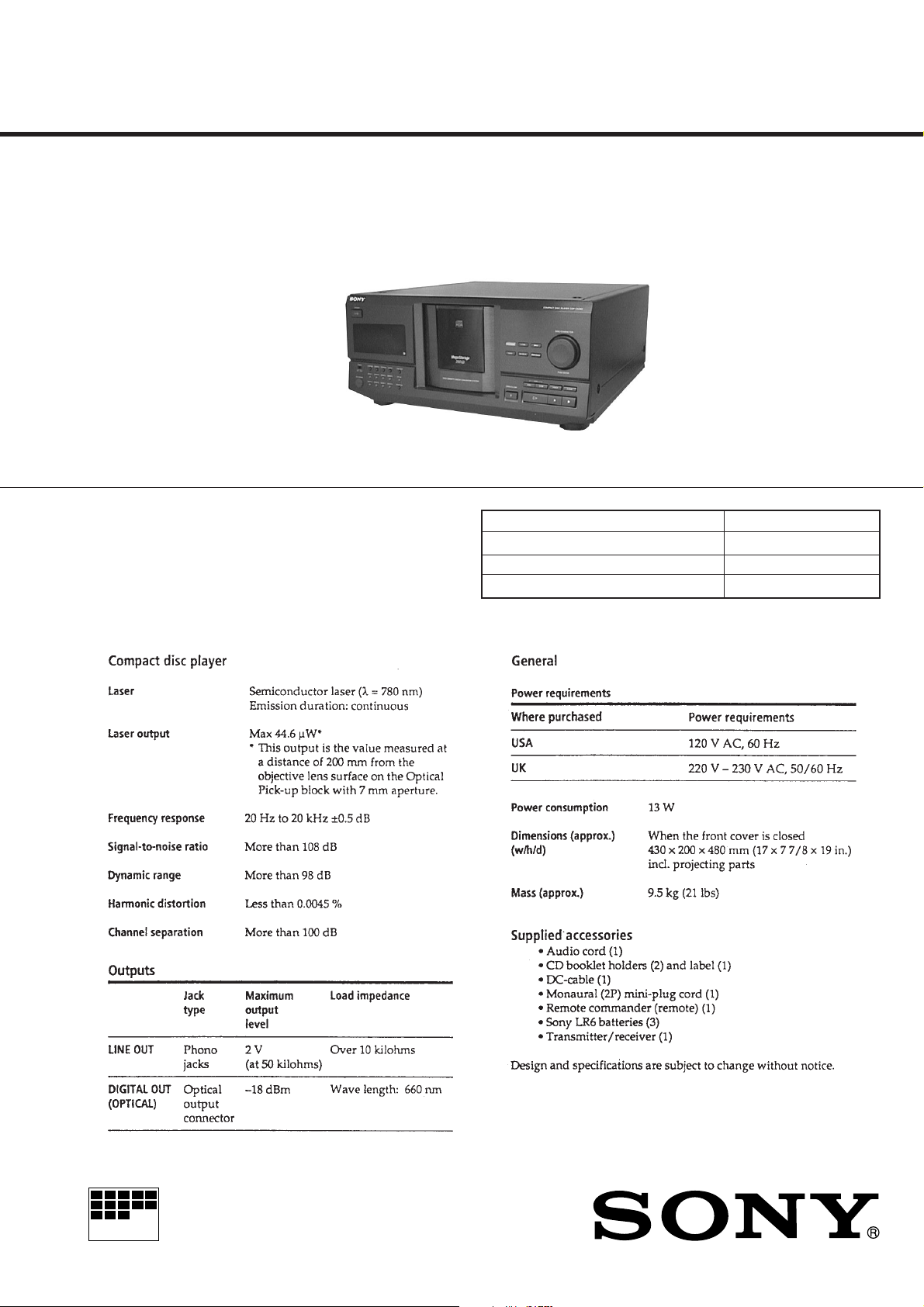
CDP-CX260
SERVICE MANUAL
Model Name Using Similar Mechanism CDP-CX200
CD Mechanism Type CDM-40B
Base Unit Type KSM-213BKN/M-N
Optical Pick-up Type KSS-213B/S-N
SPECIFICATIONS
US Model
Canadian Model
AEP Model
UK Model
COMPACT DISC PLAYER
– 1 –
Page 2
Laser component in this product is capable of emitting radiation
0.15µF
To Exposed Metal
Parts on Set
1.5k
Ω
AC
voltmeter
(0.75V)
Earth Ground
exceeding the limit for Class 1.
This appliance is classified as
a CLASS 1 LASER product.
The CLASS 1 LASER PR ODUCT MARKING is located on
the rear exterior.
The following
caution label is
located inside of
the unit.
CAUTION
Use of controls or adjustments or performance of procedures
other than those specified herein may result in hazardous radiation exposure.
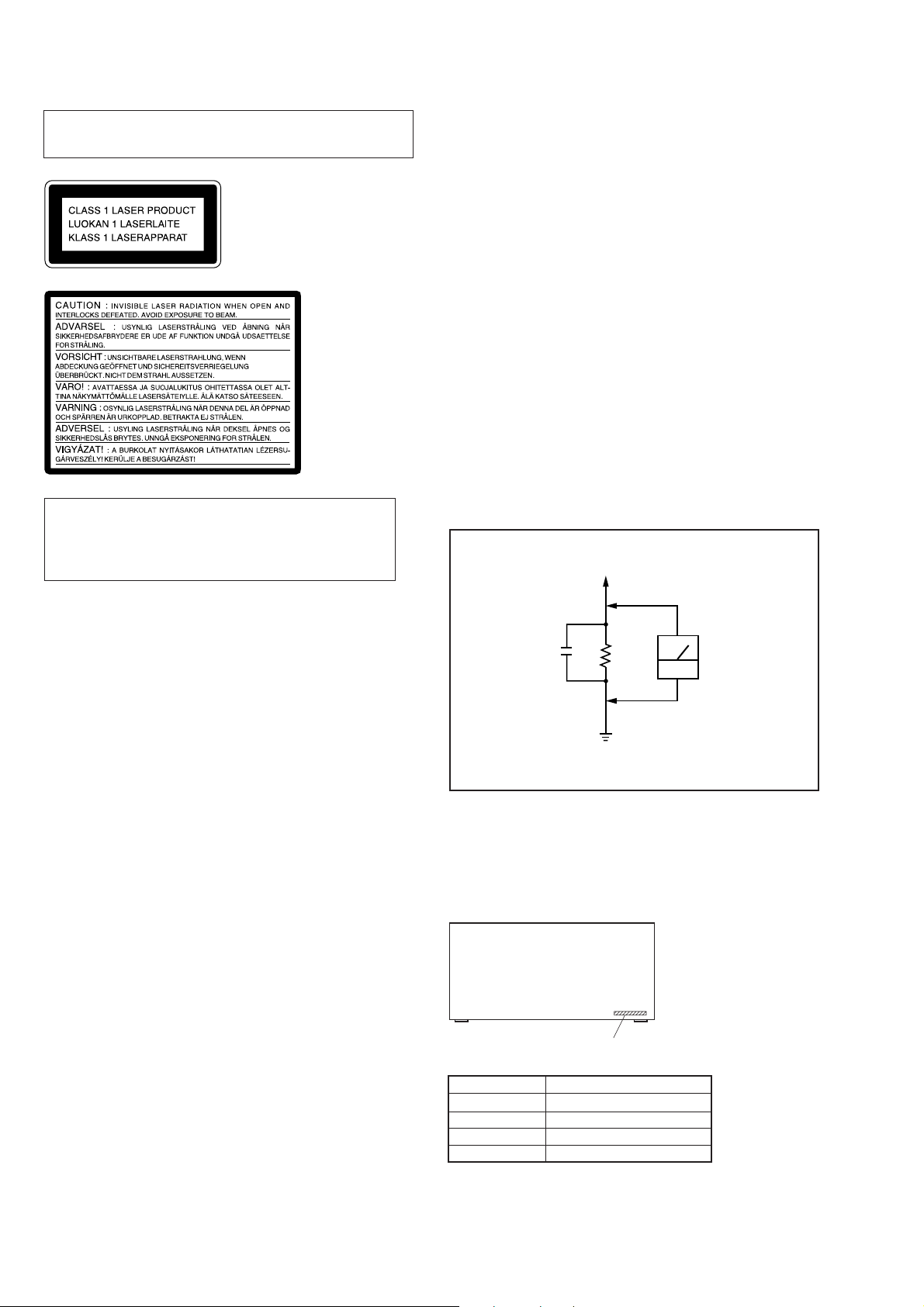
SAFETY CHECK-OUT
After correcting the original service problem, perform the following safety checks before releasing the set to the customer:
Check the antenna terminals, metal trim, “metallized” knobs, screws,
and all other exposed metal parts for AC leaka ge. Check leakage as
described below.
LEAKAGE
The AC leakage from any exposed metal part to earth Ground and
from all exposed metal parts to any exposed metal part having a
return to chassis, must not exceed 0.5 mA (500 microampers). Leakage current can be measured by any one of three methods.
1. A commercial leakage tester, such as the Simpson 229 or RCA
WT-540A. F ollow the manufacturers’ instructions to use these
instruments.
2. A battery-operated AC milliammeter. The Data Precision 245
digital multimeter is suitable for this job.
3. Measuring the voltage drop across a resistor by means of a V OM
or battery-operated AC voltmeter. The “limit” indication is 0.75
V, so analog meters must have an accurate low-voltage scale.
The Simpson 250 and Sanwa SH-63Trd are examples of a passive VOM that is suitable. Nearly all battery operated digital
multimeters that have a 2V AC range are suitable. (See Fig. A)
Notes on chip component replacement
• Never reuse a disconnected chip component.
• Notice that the minus side of a tantalum capacitor may be
damaged by heat.
Flexible Circuit Board Repairing
• Keep the temperature of soldering iron around 270˚C
during repairing.
• Do not touch the soldering iron on the same conductor of the
circuit board (within 3 times).
• Be careful not to apply force on the conductor when soldering
or unsoldering.
SAFETY-RELATED COMPONENT WARNING !!
COMPONENTS IDENTIFIED BY MARK ! OR DOTTED LINE
WITH MARK ! ON THE SCHEMATIC DIAGRAMS AND IN
THE PARTS LIST ARE CRITICAL TO SAFE OPERATION.
REPLACE THESE COMPONENTS WITH SONY PARTS
WHOSE PART NUMBERS APPEAR AS SHOWN IN THIS
MANUAL OR IN SUPPLEMENTS PUBLISHED BY SONY.
Fig. A. Using an AC voltmeter to check AC leakage.
MODEL IDENTIFICATION
— BACK PANEL —
PART NO.
ATTENTION AU COMPOSANT AYANT RAPPORT
LES COMPOSANTS IDENTIFIÉS P AR UNE MARQUE ! SUR
LES DIAGRAMMES SCHÉMATIQUES ET LA LISTE DES
PIÈCES SONT CRITIQUES POUR LA SÉCURITÉ DE
FONCTIONNEMENT . NE REMPLACER CES COMPOSANTS
QUE PAR DES PIÈCES SONY DONT LES NUMÉROS
SONT DONNÉS DANS CE MANUEL OU DANS LES
SUPPLÉMENTS PUBLIÉS P AR SONY.
À LA SÉCURITÉ!!
– 2 –
PARTS No. MODEL
4-999-021-0π
4-999-021-1π
4-999-021-2π
4-999-021-3π
US
Canadian
AEP
UK
Page 3

SECTION 1
SERVICING NOTE
TABLE OF CONTENTS
1. SERVICING NOTE .......................................................... 3
2. GENERAL .......................................................................... 6
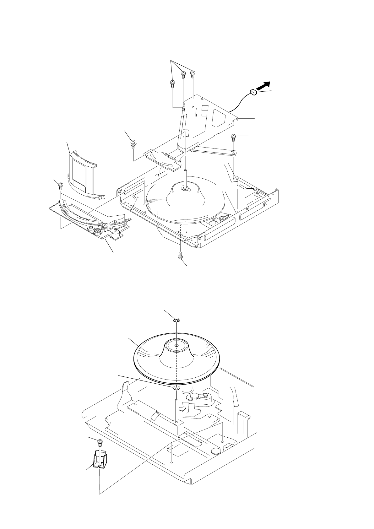
3. DISASSEMBLY
3-1. Front Panel Assembly ........................................................... 9
3-2. Back Panel Assembly............................................................ 9
3-3. Base (Door, Gear) Assembly .............................................. 10
3-4. Table Assembly ................................................................... 10
3-5. Mechanism Deck ................................................................ 11
3-6. Base Unit ...........................................................................11
4. TEST MODE ..................................................................... 12
5. ADJUSTMENTS
5-1. Mechanical Adjustment ...................................................... 15
5-2. Electrical Block Adjustment ............................................... 21
6. DIAGRAMS
6-1. Circuit Boards Location...................................................... 24
6-2. Block Diagrams
• BD Section........................................................................ 25
• Main Section..................................................................... 27
6-3. Schematic Diagram – BD Section – ................................... 31
6-4. Printed Wiring Board – BD Section – .................................33
6-5. Printed Wiring Board – Main Section –.............................. 35
6-6. Schematic Diagram – Main Section – ................................ 37
6-7. Schematic Diagram – Jack Section –.................................. 39
6-8. Printed Wiring Board – Jack Section – ............................... 41
6-9. Schematic Diagram – Display Section – ............................ 43
6-10. Printed Wiring Board – Display Section – ........................ 45
6-11. Schematic Diagram – Sensor/Motor Section – ................. 47
6-12. Printed Wiring Board – Sensor/Motor Section – .............. 48
6-13. IC Block Diagrams............................................................ 49
6-14. IC Pin Functions................................................................ 51
NOTES ON HANDLING THE OPTICAL PICK-UP BLOCK
OR BASE UNIT
The laser diode in the optical pick-up block may suffer electrostatic
break-down because of the potential difference generated by the
charged electrostatic load, etc. on clothing and the human body.
During repair, pay attention to electrostatic break-down and also
use the procedure in the printed matter which is included in the
repair parts.
The flexible board is easily damaged and should be handled with
care.
NOTES ON LASER DIODE EMISSION CHECK
The laser beam on this model is concentrated so as to be focused on
the disc reflective surface by the objective lens in the optical pickup block. Therefore, when checking the laser diode emission, observe from more than 30 cm away from the objective lens.
The emission check enables continuous checking of the S curve.
LASER DIODE AND FOCUS SEARCH OPERATION
CHECK
Carry out the “S curve check” in “CD section adjustment” and check
that the S curve waveform is output three times.
7. EXPLODED VIEWS
7-1. Case and Back Panel Section.............................................. 56
7-2. Disc Table Section .............................................................. 57
7-3. Front Panel Section ............................................................. 58
7-4. Mechanism Section-1 (CDM-40B)..................................... 59
7-5. Mechanism Section-2 (CDM-40B)..................................... 60
7-6. Mechanism Section-3 (CDM-40B)..................................... 61
7-7. Base Unit Section (KSM-213BKN/M-N)........................... 62
8. ELECTRICAL PARTS LIST ........................................ 63
– 3 –
Page 4
CD-TEXT TEST DISC
This unit is able to display the TEXT data (character information) written in the CD on its fluorescent indicator tube.
The CD-TEXT TEST DISC (TGCS-313:J-2501-126-A) is used for checking the display.
To check, perform the following procedure.
Checking Method:
1. Turn ON the po wer, set the disc on the disc table with the side labeled as “test disc” as the right side, close the front cover, and chuck the
disc.
2. The following will be displayed on the fluorescent indicator tube. (The display switches each time the TIME/TEXT button is pressed.)
Display : Main Artist Test or CD TEXT TEST DISC (Album Title)
3. Press the ” button and play back the disc.
4. The following will be displayed on the fluorescent indicator tube. (If nothing is displayed, press the TIME/TEXT button.)
Display : 1kHz/0 dB/ L&R
5. Rotate ≠ and ± buttons to switch the track. The text data of each track will be displayed.
For details of the displayed contents for each track, refer to “T able 1 : CD-TEXT TEST DISC TEXT Data Contents” and “Table 2 : CDTEXT TEST DISC Recorded Contents and Display”.
Restrictions in CD-TEXT Display
In this unit, some special characters will not be displayed properly. These will be displa yed as a space or a character resembling it. For details,
refer to “Table 2 : CD-TEXT DISC Recorded Contents and Display”.
Table 1 : CD-TEXT TEST DISC TEXT Data Contents (TRACKS No. 1 to 41:Normal Characters)
TRACK
No.
1
2
3
4
5
6
7
8
9
10
11
12
13
14
15
16
17
18
19
20
21
Displayed Contents
1kHz/0dB/L&R
20Hz/0dB/L&R
40Hz/0dB/L&R
100Hz/0dB/L&R
200Hz/0dB/L&R
500Hz/0dB/L&R
1kHz/0dB/L&R
5kHz/0dB/L&R
7kHz/0dB/L&R
10kHz/0dB/L&R
16kHz/0dB/L&R
18kHz/0dB/L&R
20kHz/0dB/L&R
1kHz/0dB/L&R
1kHz/-1dB/L&R
1kHz/-3dB/L&R
1kHz/-6dB/L&R
1kHz/-10dB/L&R
1kHz/-20dB/L&R
1kHz/-60dB/L&R
1kHz/-80dB/L&R
TRACK
No.
22
23
24
25
26
27
28
29
30
31
32
33
34
35
36
37
38
39
40
41
Displayed Contents
1kHz/-90dB/L&R
Infinity Zero w/o emphasis//L&R
Infinity Zero with emphasis//L&R
400Hz+7kHz(4:1)/0dB/L&R
400Hz+7kHz(4:1)/-10dB/L&R
19kHz+20kHz(1:1)/0dB/L&R
19kHz+20kHz(1:1)/-10dB/L&R
100Hz/0dB/L*
1kHz/0dB/L*
10kHz/0dB/L*
20kHz/0dB/L*
100Hz/0dB/R*
1kHz/0dB/R*
10kHz/0dB/R*
20kHz/0dB/R*
100Hz Squer Wave//L&R
1kHz Squer Wave//L&R
1kHz w/emphasis/-0.37dB/L&R
5kHz w/emphasis/-4.53dB/L&R
16kHz w/emphasis/-9.04dB/L&R
NOTE : The contents of Track No. 1 to 41 are the same as those of the current TEST DISC-their titles are displayed.
– 4 –
Page 5
Table 2: CD-TEXT TEST DISC Recorded Contents and Display
(In this unit, some special characters cannot be displayed. This is no a fault.)
TRACK
No.
42
43
44
45
46
47
48
49
50
51
52
53
54
55
56
57
58
59
60
61
62
63
64
65
66
67
to
99
Recorded contents Display
! ” # $%& ´ (21h to 27h)1kHz 0dB L&R
( ) + , – . / (28h to 2Fh)
*
01234567 (30h to 37h)
89 : ;<=>? (38h to 3Fh)
@A B C D E FG (40h to 47h)
H I J K L MNO (48h to 4Fh)
PQRSTUVW (50h to 57h)
X Y Z [ ¥ ] ^ _ (58h to 5Fh)
a b c d e f g (60h to 57h)
′
h i j k l m n o (68h to 6Fh)
p q r s t u v w (70h to 77h)
~
xyz{ I }
(78h to 7Fh)
i¢£¤¥ § (A0h to A7h) 8859-1
¬
≥ C ª
•±23
1
†
º ¿ (B8h to BFh)
–
PR
µ¶ • (B0h to B7h)
′
14123
(A8h to AFh)
4
АБВГДЕЖЗ (C0h to C7h)
ИЙКЛ МНОП (C8h to CFh)
DСТУФХЦ
ШЩЪЫЬY
˙
(D0h to D7h)
Я (D8h to DFh)
абвгдежз (E0h to E7h)
ийклмноп (E8h to FFh)
∂ стуфхц÷ (F0h to F7h)
шщъыьy
ÿ (F8h to FFh)
´
No.66
No.67
to
No.99
N All the same
N All the same
N All the same
N All the same
N All the same
N All the same
N All the same
X Y Z [ \ ] ^ _ (58····
N All the same
N All the same
N All the same
xyz{I}
~ (78····
i¢£¤¥ §(A0····
≥ (A8···· C ª
′
µ • (B0····•±
† ¿ (B8····
1
N All the same
N All the same
N All the same
˙
Φ ÙÚÛÜY
ß (D8····
N All the same
N All the same
∂ ñòóôoö÷(F0····
N All the same
N All the same
N All the same
to
N All the same
is not displayed
¬
PR–are not displayed
23
¶ are not displayed
14123
º are not displayed
4
– 5 –
Page 6
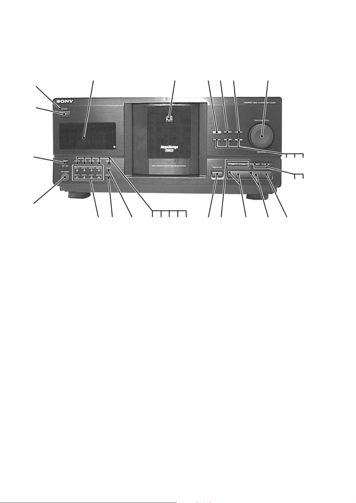
Front Panel
2
1
SECTION 2
GENERAL
345678
28
27
242526 1920212223
LOCATION OF PARTS AND CONTROLS
1 1/u (power) button
2 STANDBY indicator
3 Display window
4 Front cover
5 MEGA control button and indicator
6 X-FADE button
7 INPUT button
8 DISC/CHARACTOR dial and PUSH ENTER button
9 FADER button
10 NO DELAY button
11 MEMO SEARCH button
12 CHECK button
13 CLEAR button
14 p (stop) button
15 P (pause) button and indicator
16 · (play) button and indicator
17 ≠ AMS ± button
18 § OPEN/CLOSE button
19 TIME/TEXT button
20 REPEAT button
21 PROGRAM button
22 SHUFFLE button
23 CONTINUE button
24 HIT LIST button and indicator
25 GROUP FILE button
26 GROUP 1 to 8 button and indicator
27 KEY BOARD jack
28 TIMER (OFF/PLAY) switch
91011
12 13
1415161718
* AMS is abbreviation for Automatic Music Sensor.
– 6 –
Page 7
– 7 –
This section is extracted from
instruction manual.
Page 8
– 8 –
Page 9
SECTION 3
DISASSEMBLY
Note : Follow the disassembly procedure in the numerical order given.
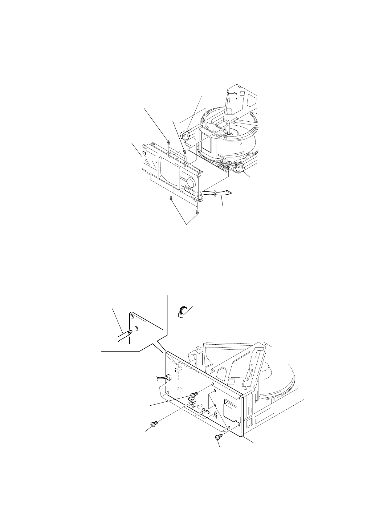
3-1. FRONT PANEL ASSEMBLY
6
Remove the claw
1
Two screws
(BVTP3x8)
2
Two screws
(BVTP 3x8)
7
Front panel assembly
5
Remove the claw
3-2. BACK PANEL ASSEMBLY
5
Remove the PC board holder
3
Four screws
(BVTT3x6)
1
4
Flat type wire (17 core)
(Main board, CN501)
Connector (CN906)
2
Two screws
(BVTT3X6)
4
Three screws
(BV3X6)
– 9 –
3
Seven screws
(BVTT3X6)
7
Back panel
Page 10
3-3. BASE (DOOR, GEAR) ASSEMBLY
)
3
Screw (PSW3x6)
6
Door (CD) assembly
8
Three screws
(BVTT3x6)
2
Three screws (BVTT3x6)
MAIN board
4
5
Guide assembly
1
Screw (BVTT3x6)
Connector (CN503
3-4. T ABLE ASSEMBL Y
2
Two screws
(BVTT3x6)
9
Base (Door, Gear) assembly
4
Table assembly
5
Washer
1
Stop ring (E type)
7
Three screws (BVTT3x6)
3
Two holder assemblies
– 10 –
Page 11
3-5. MECHANISM DECK
d
t
5
Mechanism deck
1
Flat type wire
(23core) (CN502)
Main boar
Jack board
Main board
2
Connector
(CN904)
3
Connector
(CN505)
3-6. BASE UNIT
1
Screw (BVTT3x6)
4
Nine screws
(BVTT3x8)
2
Fulcrum plate (BU Upper) assembly
3
Base uni
– 11 –
Page 12
SECTION 4
TEST MODE
4-1. DISPLAY CHECK MODE
With the power tur ned off (standby state), press the 1/u button
while pressing the P (pause) button.
All FL segments and grids light up together with the · (play),
P (pause), and STANDBY LEDs.
At the same time, the GROUP LEDs ar e lights up simultaneously .
Note: To exit this mode, press the p (stop) button.
4-2. ADJ MODE
1. Turn ON the power of the unit, set disc to disc table, and perform chucking.
2. Disconnect the power supply plug from the outlet.
3. To set ADJ mode, connect the test point (ADJ) of the MAIN
board to Ground, and connect the power supply plug to the outlet.
The power will turn on automatically, and the first track will be
played.
In this mode, table rotation and loading operations are not performed
because it is taken that the disc has already been chucked.
Note:The same operations are also performed in the follo wing when
the test point (ADJ) is connected to Ground after turning on
the power.
• Direct search (movement of sledding motor) is not performed dur -
ing accessing
• Ignored even when GFS becomes L
• Ignored even when the Q data cannot be read
• Focus gain does not decrease
• Spindle gain does not decrease
• Servo related settings can be set manually and checked (Refer to
ADJ Mode Special Functions Table)
ADJ Mode Special Functions Table
(The buttons shown with ( ) function by using the supplied remote commander only)
Button
CONTINUE
SHUFFLE
PROGRAM
GROUP 1 (1)
GROUP 2 (2)
GROUP 3 (3)
GROUP 4 (4)
GROUP 5 (5)
GROUP 6 (6)
GROUP 7 (7)
GROUP 8 (8)
(9)
(10/0)
CHECK
CLEAR
Servo average display
Displays VC, FE, RF, TE and traverse in hexadecimal
numbers
Focus bias display
Each time this is pressed, the focus bias is switched
between 1 and 2
(1)
Bias actually set Optimum bias Minimum jitter
(2)
U:Upper aliasing bias L:Lower aliasing bias
Auto gain display
Displays focus, tracking, sledding in hexadecimal
numbers
Increases the focus bias in 8 steps.
Sets the focus bias in the middle of aliasing.
Turns off the tracking and sledding servo
Returns the auto gain to the initial value (30)
Turns off the focus servo
Decreases the focus bias in 8 steps.
Re-adjusts the focus bias
Turns on the tracking and sledding servo
Switches the focus servo gain between normal and down
FG. norm: normal, FG. down: down
Sets the focus bias to 0 (no bias)
Next, displays the jitter measured at the focus bias set
S-curve observation mode.
(Exits this mode when the p button is pressed.)
Automatic eccentric measurement
The results of measurement is displayed in µm directly.
Function
4-3. KEY AND DISPLAY CHECK MODE
To set this mode , connect the test point (AFADJ) on the MAIN
board to Ground, and connect the power supply plug to the outlet.
• All FL segments and grids will light up. (All lit check)
When a button is pressed, the types of buttons pressed until then
will be displayed on the left side and the number of the buttons
will be displayed on the right side. However, these will not be
displayed for the following special buttons.
p (stop) button: FL segment check
(Refer to FL Tube Check Patterns)
P (pause) button: FL grid check
(Refer to FL Tube Check Patterns)
The pause LED also lights up simultaneously .
· (play) button:All FL segment and grid will light up.
The play LED also lights up simultaneously.
FL Tube Check Patterns
Segment check
Magnified
Grid check
ABCDE
• When the jog dial is rotated to the right, the GROUP LEDs light
up in the order of 1n2..8n1.
• When the jog dial is rotated to the left, the GR OUP LEDs light up
in the order of 8n7..1n8.
• Abbreviation
FL: Fluorescent Indicator Tube
[ MAIN BOARD ] – Component Side –
CN506
6
1
RV501
DISC SENSOR
ADJUSTMENT
R531
TP1
(ADJ)
TP2
(AFADJ)
R540
IC501
– 12 –
Page 13
4-4. AGING MODE
1DISC
CD1
DISC
*DISC-40*
2
number of agings
Aging Mode
• Mode which repeatedly changes and plays back discs automatically in the unit.
• It will repeat aging as long as no errors occur.
• If an error occurs during aging, it will stop all servos, motors, etc.
instantaneously, display the error number, and stop operations.
However , the stopping conditions dif fer according to whether the
unit is equipped with the “self-protection function during errors”
described later.
The function serves to maintain the state of the unit when errors
occur.
Sequence of Aging Mode
$
1. Disc change
$
2. Load in
$
3. TOC read
$
4. Access of last track
$
5. 3 second playback
$
6. Access of first track
$
7. 3 second playback
Order of Disc Change
(1 cycle takes 3 minutes)
$
1. No. 40
$
2. No. 80
$
3. No. 120
$
4. No. 160
$
5. No. 200
$
Special Aging Mode Functions
The aging mode is provided with the following con venient functions
• Disc setting mode (*1)
• Selection of presence of protection function during error (*2)
• Count function of aging cycle (*3)
*1 Disc setting mode:
5 discs are set before setting the aging mode. This mode makes
the setting of these discs more easy.
*2 Self protection function during errors:
Function which voluntarily corrects errors which occur during
normal operations by retries.
If this function is not provided, all operations will be stopped
without retiring. It is suitable for checking errors with low reproducibility.
If this function is provided, and errors can be corrected by retries,
aging will be continued without stopping.
*3 Aging cycle count function:
Functions which displays the number of agings carried out on
the Fluorescent indicator tube in numbers. One aging cycle consists of five discs.
$
8. Load out
$
9. FRONT COVER open
$
10. FRONT COVER close
$
– 13 –
Page 14
Aging Method
1. Turn ON the po wer of the unit. Press the § OPEN/CLOSE and
open the front cover.
2. Change the COMMAND MODE switch (S901) on set to CD1 .
3. Press the AGING START button of the remote commander for
aging mode (J-2501-123-A).
4. When the disc set mode is set, the ( and P LEDs blink.
5. Rotate the DISC/CHARACTER dial. The slits (No. 40, 80,
120, 160, 200) for setting the discs will come forward. Insert the
discs into these slits. Do not set the discs in other slits.
6. Set whether the self-protection function during errors is equipped
with the unit. Press the REPEAT button. If “REPEAT” is displayed on the Fluorescent indicator tube, it means the function
is provided. If “REPEA T” is not displayed, it means the function
is not provided.
Error Display
120 Err01
Disc number Error code
Error code
Err 01
Err 02
Err 03
Err 04
Err 05
Err 06
Err *1
Err *2
Err *3
Err *4
Err *5
Err *6
Err *7
DISC sensor check 1
DISC sensor check 2
Table operation check 1
Table operation check 2
Loading operation check 1
Loading operation check 2
BU related check 1
BU related check 2
BU related check 3
BU related check 4
BU related check 5
BU related check 6
BU related check 7
7. Press the ( button.
8. The ( LED blinks, the aging mode is set, and aging is started.
9. The aging cycle lasts 3 min utes. If errors occur during aging, the
error number will be displayed on the Fluorescent indicator tube.
(Refer to the following table for the details of the errors.)
10. Aging will be repeated as long as no errors occur.
11. After each aging cycle, the number displayed on the Fluorescent
indicator tube will increase.
12. To end aging, press the 1/u button.
ContentsCode number Name
No disc in the specified slit
Disc in other slits
Table motor current over
No table sensor input
Load in timeover
Load out timeover
Access timeover
High speed search NG
Q data read error
BU operation (from focus search to until signal can be read) timeover
GFS monitor error
Focus cannot be imposed by focus search
Auto focus bias adjustment cannot be performed
The * numbers mean the following according to the state of the unit during aging
2 : From chucking to end of TOC read
3 : From end of TOC read to end of last track playback
4 : From end of last track playback to end of first track playback
– 14 –
Page 15
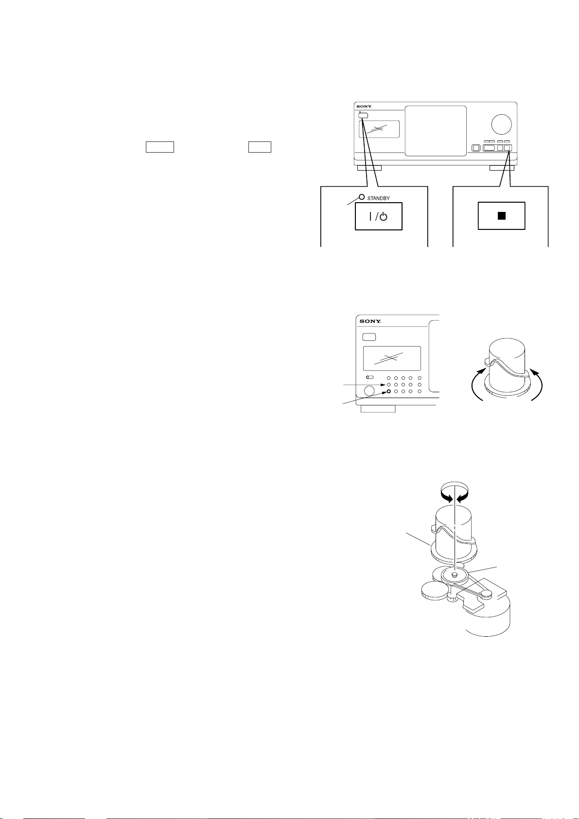
SECTION 5
ADJUSTMENTS
5-1. MECHANICAL ADJUSTMENT
Perform the following steps before carrying out adjustments.
1. Turn ON the po wer of the unit, set disc to disc table No. 92, and
perform chucking.
2. Turn OFF the power.
3. Remove the case.
4. While pressing the STOP button, turn ON the 1/u button.
The test mode is set.
5. The POWER button LED starts blinking.
(Test mode)
LED
1/u
button STOP button
NOTE 1: The cam will start rotating when the GR OUP 1 or GROUP
5 button is pressed continuously in the test mode.
NOTE 2: If the power cannot be supplied, the cam can be rotated
by rotating the pulley with your finger.
GROUP 1
button
GROUP 5
button
Cam
GROUP 1
button
GROUP 5
button
Pulley
– 15 –
Page 16
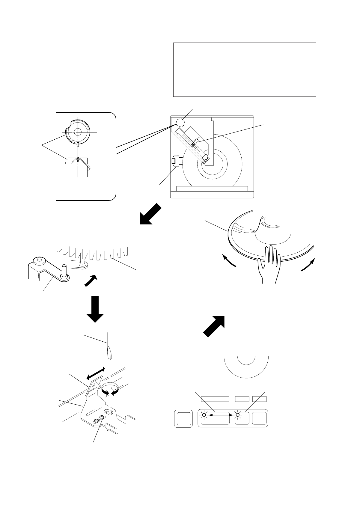
GUIDE (DISC T) ALIGNMENT
Cam
Cam Holder (guide T)
(1) Rotate the cam and adjust to the
position shown in the figure.
(2) Check that the state is as
shown in the figure.
A
B
Guide (disc T)
Disc
Guide (disc T)
Fixed screw
Guide (disc T)
Disc
(3) Loosen the fixed screw by about 60 °.
Holder
(guide T)
Tapering screwdriver
Holder (guide T)
(4) Move the holder (guide T) with a tapering screwdri ver ,
and set the position of the guide (disc T) to A:B=1:1.
– 16 –
Page 17
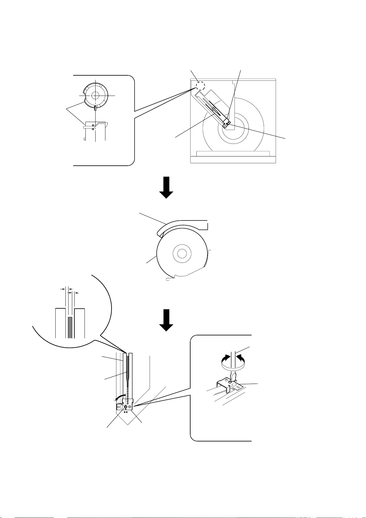
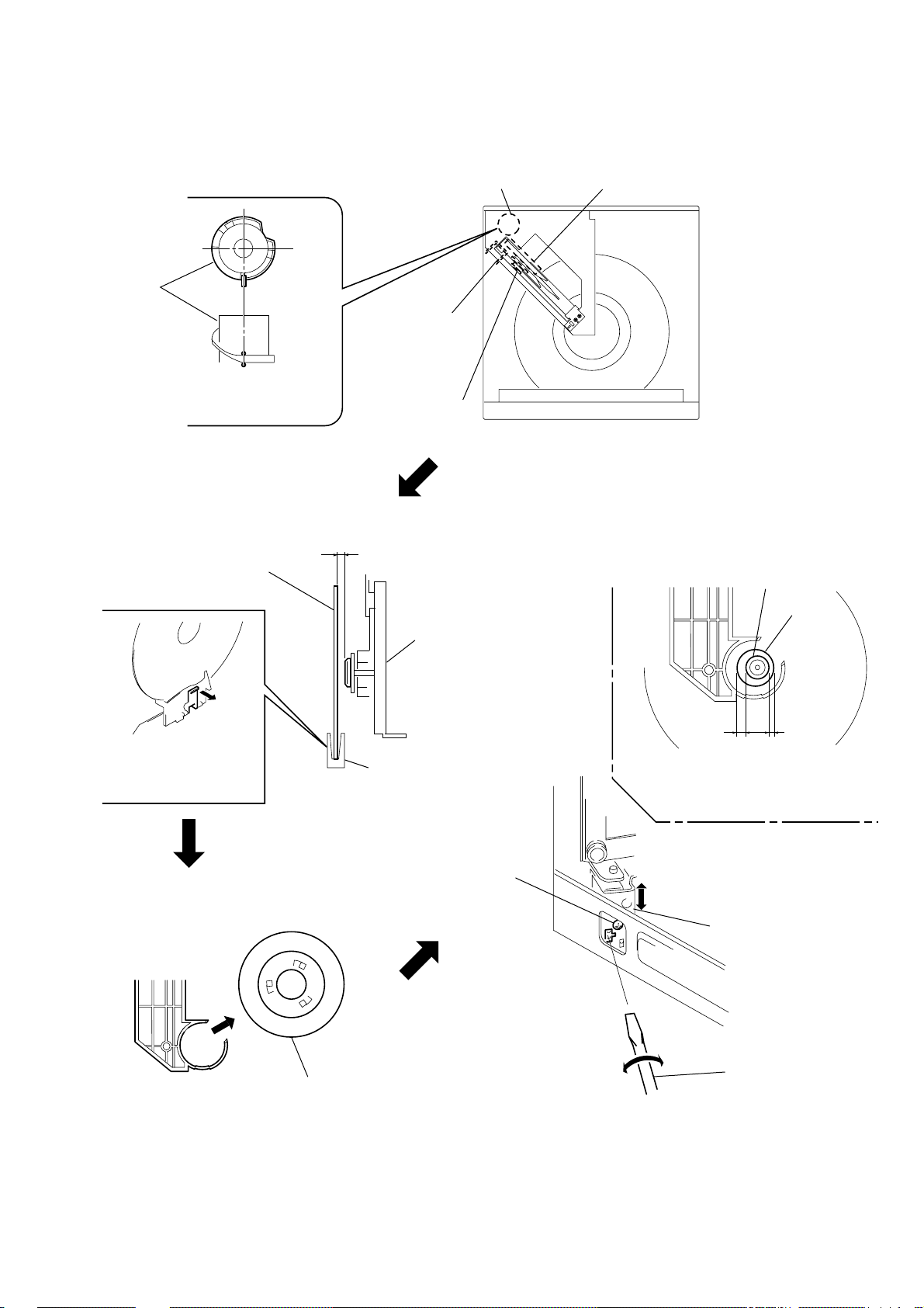
HOLDER (DISC A) ALIGNMENT
Cam
(1) Rotate the cam and adjust to the
position shown in the figure.
Cam Holder (disc A)
Thrust
screw
Disc
0 - 1mm
(2) Check that the state is as shown in
Thrust screw
Holder (disc A)
the figure.
Disc
Holder (disc A)
(3) After applying suitable locking compound to the part, rotate the thrust screw until the holder (Disc A) comes to the center of the disc .
– 17 –
Page 18
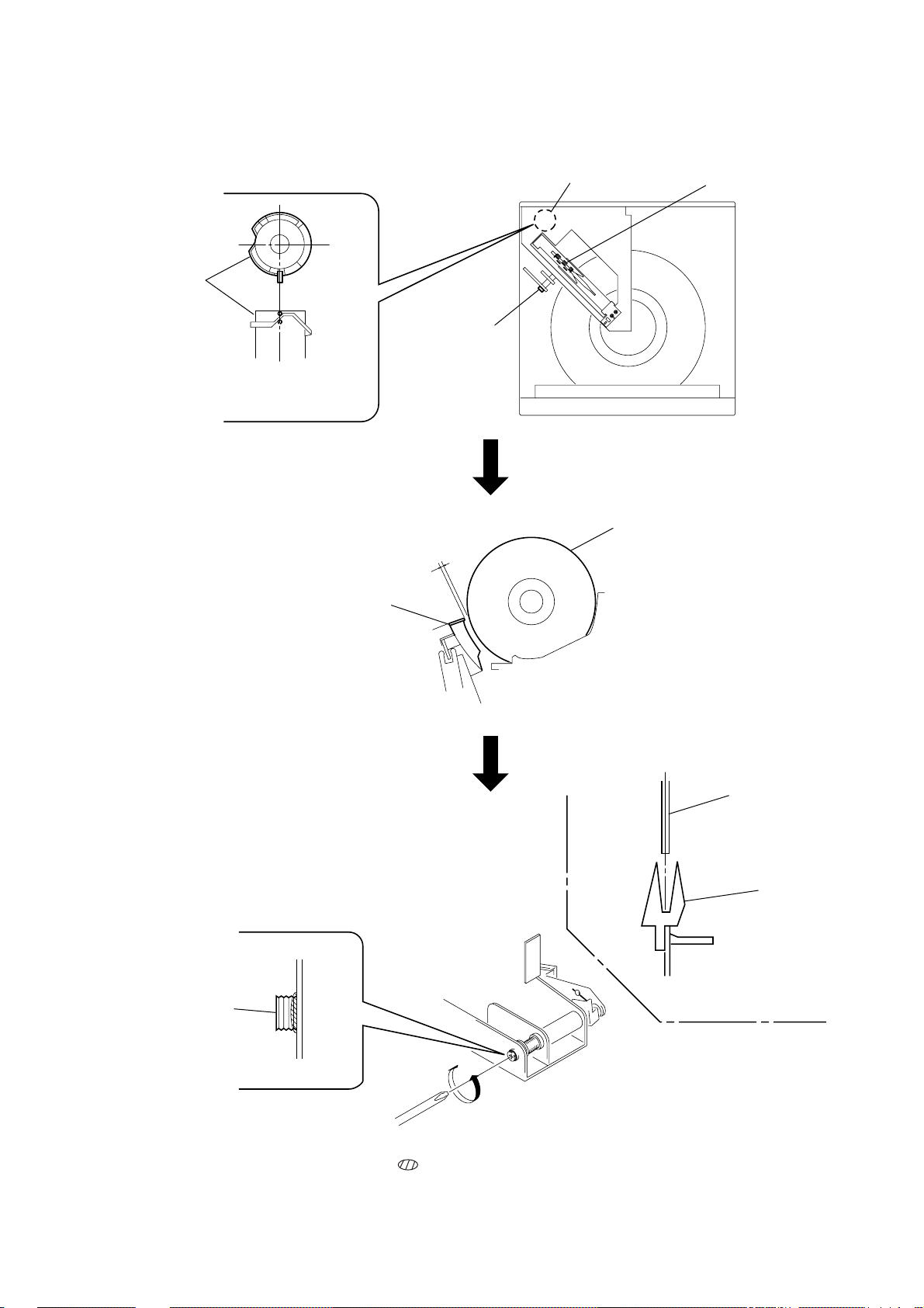
SENSOR ALIGNMENT
Perform this adjustment after the “holder (disc A) adjustment”.
If the disc table swings to the left and right just before the disc is
chucked, perform the following adjustment.
Cam
CAUTION:
The LED may not light up in steps (3) and (4) for some
microprocessor versions, and consequently adjustments will not
be possible.
In this case, fix the bracket (sensor) at the mechanical center.
As fine adjustments need to be performed in “Disc Sensor
Adjustment” in Electrical Adjustments, sensor alignment need
not be performed here.
Cam
Lever (stopper)
assembly
(1) Rotate the cam and adjust to the
position shown in the figure.
(2) Check that the lever (stopper) assembly
secures the disc table as shown in the figure.
Lever (stopper) assembly
Tapering screwdriver
Bracket (sensor)
Disc table
Table assembly
Swing
(4) Moving the disc table right and left with a hand after the scre w
is fixed, the table will move by the play of a disc table. If the
LEDs light up alternately, the adjustment will be performed
correctly.
Luminus board
PAUSE buttonPLAY button
Bracket (sensor)
Fixed screw
(3) Loosen the fixed screw by 60° to 90°, and use a tapering screwdriver to adjust the screw as shown in the figure.
Move the bracket (sensor) with the tapering screwdriver little by little, and fix the fixed screw at where the play button's LED (green) is
switched to the pause button's LED (orange) (or its reverse).
– 18 –
Page 19
PULLY AND DISC CENTER HOLE ALIGNMENT
Cam
Bracket
(BU adjustment)
(1) Rotate the cam and adjust to the
position shown in the figure.
Magnet assembly
(2) Check that the state is as shown
in the figure.
0.5 - 2mm
Disc
Cam Base unit
Disc pulley
Note:The disc should not
be fixed.
Disc hole
Base unit
AB
Holder (disc A)
Fixed screw
Bracket
(BU adjustment)
Magnet assembly
(3) Remove the Magnet assembly.
Tapering screwdriver
Loosen the fixed screw by 60° to 90°, and move and adjust the
bracket (BU adjustment) up and down using a tapering screwdri ver
so that the positions of the disc hole and disc pulley become A=B
or between A:B=2:1 and 1:2.
– 19 –
Page 20

MAGNET ASSY ALIGNMENT
Cam
(1) Rotate the cam and adjust to the
position shown in the figure.
Cam
Adjustment
screw
Magnet assembly
Adjustment
screw
(3) Apply suitable locking compaund to the part after adjusting.
Magnet holder
Magnet assembly
Disc
AB
Adjustment
screw
– 20 –
(2) Rotate the adjustment screw until A=B or between
A:B=2:1 and 1:2
Page 21

5-2. ELECTRICAL BLOCK ADJUSTMENT
0V
C (DC
voltage)
Tracking servo
Sledding servo
OFF
Tracking servo
Sledding servo
ON
Note:
1. CD Block is basically designed to operate without adjustment.
Therefore, check each item in order given.
2. Use YEDS-18 disc (3-702-101-01) unless otherwise indicated.
3. Use an oscilloscope with more than 10MΩ impedance.
4. Clean the object lens by an applicator with neutral detergent when
the signal level is low than specified value with the following
checks.
Note: A clear RF signal waveform means that the shape “◊” can be
clearly distinguished at the center of the waveform.
RF signal waveform
VOLT/DIV : 200mV
TIME/DIV : 500ns
level : 1.2 Vp-p
+0.25
–0.20
S-Curve Check
oscilloscope
BD board
TP (FE1)
TP (VC)
Procedure :
1. Chuck the disc (YEDS-18) beforehand, and disconnect the power
cord from the outlet.
2. Connect oscilloscope to test point TP (FE1) on BD board.
3. Connect test point TP1 (ADJ) on MAIN board to ground with
lead wire.
4. The ADJ mode is set when the power cord is inserted into the
outlet and power is supplied.
5. The fifth track is played automatically.
6. Press the CHECK button.
7. Check the oscilloscope waveform (S-curve) is symmetrical between A and B. And confirm peak to peak level within 3±1 Vp-p.
S-curve wavef orm
symmetry
A
Within 3
±
1 Vp-p
B
E-F Balance Check
oscilloscope
BD board
TP (TE)
TP (VC)
Procedure :
1. Chuck the disc (YEDS-18) beforehand, and disconnect the power
cord from the outlet.
2. Connect oscilloscpe to test point TP (TE) on BD board.
3. Connect test point TP1 (ADJ) on MAIN board to ground with
lead wire.
4. The ADJ mode is set when the power cord is inserted into the
outlet and power is supplied.
5. The fifth track is played automatically.
6. Press the GROUP 3 button. (The tracking servo and the sledding servo are turned OFF.)
7. Check the level B of the oscilliscope's waveform and the A (DC
voltage) of the center of the Traverse waveform.
Confirm the following :
A/B x 100 = less than ± 22%
Traverse waveform
Center of the waveform
B
8. Pressing the p button stops the output of the wav eform (s curve).
9. After check, remove the lead wire connected in step 3.
Note : • Try to measure sev eral times to make sure than the ratio of
A : B or B : A is more than 10 : 7.
• Tak e sweep time as long as possible and light up the brightness to obtain best waveform.
RF Level Check
oscilloscope
BD board
TP (RF)
TP (VC)
Procedure :
1. Connect oscilloscope to test point TP (RF) on BD board.
2. Turn Power switch on.
3. Put disc (YEDS-18) in to play the number five track.
4. Confirm that oscilloscope wav eform is clear and check RF signal
level is correct or not.
0V
level : 1.3 ± 0.6 mVp-p
A (DC voltage)
8. Press the GROUP 8 button. (The tracking servo and sledding
servo are turned ON.) Confirm the C (DC voltage) is almost
equal to the A (DC voltage) is step 7.
Traverse waveform
9. Disconnect the lead wire of TP1 (ADJ) connected in step 2.
– 21 –
Page 22

Disc Sensor Adjustment
e
0
d
Perform this adjustment after completing all adjustments of the
mechanism section.
If not performed accurately, the presence of the disc may not be
detected properly.
Connection 1:
CN506 of MAIN board
1
T1 : Pin
T2 : Pin
D0 : Pin
(TS. 1)
2
(TS. 2)
4
(D. SENS)
1 k
Ω
oscilloscop
Waveform 1:
AB
T1
T2
D
Procedure:
1. Connect the oscilloscope to Pins 1, 2, and 4 of CN506 of the
MAIN board. Also connect a 1 kΩ resistor to Pin 4 at the same
time. (Connection 1)
2. Check that no discs are loaded in the unit.
3. With the power OFF, press the 1/u button while pressing the
INPUT button, and turn on the power at the same time.
4. The rotary table will continue rotating in the clockwise direction.
5. Observe the waveform at that time on the oscilloscope.
6. Loosen the screw securing the D.SENS (LUMINOUS) board
slightly.
7. Slide the D.SENS (LUMINOUS) board to the left and right so
that the peak of the D0 waveform is at the center between the
descending point of the T1 waveform and ascending point of the
T2 waveform. (Waveform 1) After adjusting, apply locking
compound.
D.SENS (LUMINOUS) boar
Connection 2:
CN506 of MAIN board
T1 : Pin
T2 : Pin
D1 : Pin
Waveform 2
XZY
1
(TS. 1)
2
(TS. 2)
4
(D. SENS)
oscilloscope
T1
T2
D1
8. Disconnect the resistor connected to Pin 4 of CN506 of the
MAIN board. (Connection 2)
9. Observe the waveform on the oscilloscope. (Waveform 2)
10. Adjust RV501 of the MAIN board so that the waveform on the
oscilloscope satisfies the following adjustment value 1.
11. Press the 1/u button and turn OFF the power.
12. Press the 1/u button, turn on the power, press the OPEN/
CLOSE button, and open the front cover . Next rotate the DISC/
CHARACTER dial in the counterclockwise direction
continuously so that the rotary table rotates continuously in the
counterclockwise direction.
13. Observe the waveform on the oscilloscope and confirm that it
satisfies the adjustment value 2 (waveform 3). If it does not,
adjust RV501 of the MAIN board.
Waveform 3:
XZY
T1
T2
D1
– 22 –
Page 23

14. After the adjustment, load a disc only in slit 1, and press the 1/
u button to turn off the power.
15. Press the 1/u button while pressing the PUSH ENTER button
to turn on the power.
16. If the rotary table makes one round, and “YES” is displayed on
the fluorescent indicator tube after it stops, it means that the
adjustment has been performed properly.
Adjustment value 1:
At the shoulder part of waveform D1, T1 becomes H and T2 becomes L, and at the same time, the Y width must not be smaller
than 1/4 of the Z width.
In order to satisfy this value more easily, adjust so that X=Y approximately and observe the deviation of the waveform.
Adjustment value 2:
At the shoulder part of waveform D1, T1 becomes L and T2 becomes H, and at the same time, the Y width must not be smaller
than 1/4 of the Z width.
Adjustment Location :
[ BD BOARD ] – Side B –
TP
(VC)
TP
(TE)
IC102
TP
(RF)
TP
(FE1)
IC103
[ MAIN BOARD ] – Component Side –
R540
TP2
(AFADJ)
IC501
CN506
6
1
RV501
DISC SENSOR
ADJUSTMENT
R531
TP1
(ADJ)
– 23 –
Page 24

6-1. CIRCUIT BOARDS LOCATION
d
SECTION 6
DIAGRAMS
DISP board
KEY BOARD board
T.SENS board
JOG board
D.SENS (LUMINOUS) board
ILLUMINATION board
MAIN board
JACK boar
T.MOTOR board
D.SENS (RAY-CATCHER) board
DOOR MOTOR boardDOOR SW board
BD board
L.SW board
L.MOTOR board
– 24 –
Page 25

CDP-CX260
6-2. BLOCK DIAGRAMS
– BD SECTION –
OPTICAL PICK-UP
BLOCK (KSS-213B)
LASER
DIODE
PB
DETECTOR
E
PD1
PD2
F
LD
POWER
LD
LD
DRIVE
Q101
4
IC101
DIGITAL SIGNAL PROCESSOR
IC103
RF AMP
4
3
5
6
7
8
10
11
APC LD
AMP
SUMMING
AMP
TRACKING
ERROR
AMP
VC
BUFFER
DOUT
LOUT
ROUT
SYSM
LMUT
SCOR
SQCK
SQSO
DATA
XLAT
CLOK
SENS
60 3
72
75
4
80
79
20
2
1
5
6
7
8
SERVO
INTERFACE
DIGITAL
OUT
OVER
SAMPLING
DIGITAL
FILTER
SUBCODE
PROCESSOR
3rd ORDER
NOISE
SHAPER
PWM
CPU
INTERFACE
SERVO
AUTO
SEQUENCER
21
22
RF
FOCUS
ERROR
AMP
RF EQ
AMP
16
14
13
12
VC
LPF
LPF
X101
16.9MHz
ASYO
48
16K
RFAC
51
ASYI
ASYMMETRY
49
CORRECTION
VC
VC
38
CE
42
RFDC
43
TE
41
40
39
14
66
67
SE
FE
XLON
XTAI
XTAO
A/D
CONVERTER
TIMING
LOGIC
DIGITAL
PLL
DEMODULATOR
MIRR
DFCT
FOK
DETECTOR
EFM
FOK
DFCT
MIRR
DIGITAL
CLV
INTERNAL BUS
ERROR
CORRECTION
RAM
D/A
INTERFACE
SERIAL
IN
INTERFACE
IC901
DIGITAL
OUT
OPTICAL
LOUT
R ch
LMUTE
DATA
CLOK
SCOR
SENS
SYSM
XLAT
SQCK
SQSO
A
MAIN
SECTION
SERVO DSP
FOCUS
SERVO
TRACKING
SERVO
FOCUS/TRACKING COIL DRIVE,
T+
TRACKING
COIL
FOCUS
COIL
M102
SLED
MOTOR
M101
SPINDLE
MOTOR
09
1
T–
2
F–
16
F+
17
13
M
12
27
M
26
IC102
SPINDLE/SLED MOTOR DRIVE
MUTE
4
5
19
20
10
9
VC
23
24
15
D+5V
LPF
S101
LIMIT
SSTP
27
TFDR
30
TRDR
31
FFDR
32
FRDR
33
SRDR
29
SFDR
28
MDP
26
SLED
SERVO
PWM
GENERATOR
TRACKING
PWM
GENERATOR
FOCUS
PWM
GENERATOR
SLED
PWM
GENERATOR
XRST
SCLK
3
9
XRST
SCLK
AGC
• Rch is same as Lch.
• SIGNAL PATH
:CD
: CD (digital)
– 25 – – 26 –
Page 26

CDP-CX260
– MAIN SECTION –
LOUT
LMUTE
CLOK
DATA
SCOR
SENS
SYSM
XLAT
SQCK
A
BD
SECTION
SQSO
XRST
SCLK
M802
LOADING
MOTOR
M810
DOOR
MOTOR
M801
TABLE
MOTOR
M
M
M
DISC(A) SENSOR
3
9
4
IC802
IC503
MOTOR DRIVE
LOADING
MOTOR
DRIVE
DOOR
MOTOR
DRIVE
TABLE
MOTOR
DRIVE
IC803
DISC(B) SENSOR
IC801
ADDRESS SENSOR
SQSO
J903
MUTE
Q324
IC401
AMP
3
1
2
MUTE
CONTROL
SWITCH
Q325-329
48
CLK
DATA
50
54
SENS
SCOR
61
47
AMUTE
49
XLAT
51
SQCK
SUBQ
52
1
2
8
26
27
24
237
215
226
63
62
64
LDIN
LDOUT
DROUT
DRIN
TBLL
TBLR
T.S 2
T.S 1
T.S 3
SMUTE
EXTAL
XTAL
DOORSW
INSW
OUTSW
D.SENS
ADJ
AFADJ
29
31
32
39
67
55
38
RV501
DISC SENSOR
25
57
X501
10MHz
(ADJ)
(AFADJ)
Q801, D801
TP1
TP2
LOADING
DISC
SENSOR
S801
DET
S810
DOOR
DET
MUTE
Q321
J821
KEY BOARD
B+
SYSTEM CONTROLLER
CHARACTER
KEY MATRIX
S611 - 617,
S621 - 627,
S721 - 728,
S731 - 738
IC501
DISC/
S901 COMMAND MODE
2
3
SWITCH
Q511,512
CD
1 2 3
IC302(1/2)
LPF
JOG
RE601
CD3
CD2
CD1
IC302(2/2)
MIX AMP
1
6
7
5
MUTE
Q322,323
3 1
30
60
17
15
16
40
42
45
KBCIN
KBDIN
KBCOUT
KBDOUT
CD1/2/3
KEY 3
KEY 0
RST
ICSW
CE
WE
D00
D07
A0
A14
FL DATA
FL CLK
FLLT
LEDLT
RM IN
2ND CD IN
L
LINE OUT
L
D+5V
IC505
RESET
D802-D804
INSIDE
ILLUMINATION
65
14
13
68
71
•
74
77
78
80
•
1
12
VF1 VF1
DATA
18
CLK
19
58
20
REMOTE
CONTROL RECEIVER
56
1
–VCC
IC504
+5V
3 1
REG
M+5V
IC506
RESET
+5V/+7V REGULATOR
+VCC
6
RST
2
IC601
RM
+5V
+7V
Q521
VO
9
FL701 FLUORESCENT INDICATOR TUBE
1
•
3
1G-15G P1-P3616G
60 - 46 32 - 41,30 - 6,31
40 - 54 4 - 39
DIG01 DIG15 DIG16
SCK
62
63 61 60 56
CLK
DATA
DA
10
1
+VCC
EN2
8
EN1
4
IC502 S-RAM
20
CE
WE
27
11
D0
13
•
15
19
D7
CS
RESET
D508
BUFFER
Q701
DATA
CLK
+VCC
45
55
4
8
7
6
D509
10
A0
26
23
A14
21
IC701
FL DRIVER
DATA
CLK
RST
LT
VFL
VF1
FL701
VF2
D503, 504
RECT
SWITCH
Q503
1
•
•
11 - 14,16 - 24
LED
D507
IC702
LED DRIVER
D501, 502
RECT
AD1,SEG01 SEG35
D601-604
D701-710
–30V REG
Q501
D505
–B
RECT
D902, 903
RECT
• Rch is same as Lch.
• SIGNAL PATH
: CD
VF2 VF2
VFL
VFL
AU BUS
BUFFER
TRANSFORMER
63
•
65
Q901
T901
POWER
+6V
1 3
REG
L901
LINE
FILTER
AC IN
J905
TO REMOTE
SENSOR UNIT
DC OUT 6V
J901, 902
S-LINK
CONTROL A1
66
AGC
09
RFSW
– 27 –
BUS OUT
BUS IN
28
46
– 28 –
Page 27

THIS NOTE IS COMMON FOR PRINTED WIRING
(
)
7.5µsec
2.4Vp-p
2.5V
APPROX 200m Vp-p (PLAY)
BOARDS AND SCHEMATIC DIAGRAMS.
(In addition to this, the necessary note is printed
in each block.)
WAVEFORMS
1
3.1Vp-p
For schematic diagrams.
Note:
• All capacitors are in µF unless otherwise noted. pF: µµF
50 WV or less are not indicated except for electrolytics
and tantalums.
• All resistors are in Ω and
1
/4 W or less unless otherwise
specified.
¢
•
: internal component.
• C : panel designation.
Note:
The components identified by mark ! or dotted
line with mark ! are critical for safety.
Replace only with part
number specified.
Note:
Les composants identifiés par
une marque ! sont critiques
pour la sécurité.
Ne les remplacer que par une
piéce portant le numéro
spécifié.
• U : B+ Line.
• V : B– Line.
• H : adjustment for repair.
• Voltages and waveforms are dc with respect to ground
under no-signal (detuned) conditions.
no mark : STOP
• Voltages are taken with a V OM (Input impedance 10 MΩ).
Voltage variations may be noted due to normal production tolerances.
• Waveforms are taken with a oscilloscope.
Voltage variations may be noted due to normal production tolerances.
• Circled numbers refer to waveforms.
• Signal path.
J : CD
c : digital out
For printed wiring boards.
Note:
• X : parts extracted from the component side.
• Y : parts extracted from the conductor side.
®
•
• b : Pattern from the side which enables seeing.
(The other layers' patterns are not indicated.)
: Through hole.
2
3
APPROX 500mVp-p
4
5
6
16.9MHz
IC101 ^§ XTAI
1.2Vp-p
(PLAY)
IC101 %¡ RF AC
2.5V
PLAY
IC101 $¡ TE
IC101 #ª FE
IC101 @§ MDP
3.8Vp-p
10MHz
IC501 #¡ EXTAL
Caution:
Pattern face side: Parts on the pattern face side seen from the
(Side B) pattern face are indicated.
Parts face side: Parts on the parts face side seen from the
(Side A) parts face are indicated.
• Indication of transistor
C
Q
C
These are omitted
EB
EB
These are omitted
– 29 – – 30 –
Page 28

THIS NOTE IS COMMON FOR PRINTED WIRING
BOARDS AND SCHEMA TIC DIAGRAMS.
(In addition to this, the necessary note is printed
in each block.)
For schematic diagrams.
Note:
• All capacitors are in µF unless otherwise noted. pF: µµF
50 WV or less are not indicated except for electrolytics
and tantalums.
• All resistors are in Ω and
specified.
¢
•
: internal component.
1
4
/
W or less unless otherwise
• C : panel designation.
Note:
The components identified by mark ! or dotted
line with mark ! are critical for safety.
Replace only with part
number specified.
Note:
Les composants identifiés par
une marque ! sont critiques
pour la sécurité.
Ne les remplacer que par une
piéce portant le numéro
spécifié.
• U : B+ Line.
• V : B– Line.
• H : adjustment for repair.
• Voltages and waveforms are dc with respect to ground
under no-signal (detuned) conditions.
no mark : STOP
• Voltages are taken with a VOM (Input impedance 10 MΩ).
Voltage variations may be noted due to normal production tolerances.
• Waveforms are taken with a oscilloscope.
Voltage variations may be noted due to normal production tolerances.
• Circled numbers refer to waveforms.
• Signal path.
J : CD
c : digital out
For printed wiring boards.
Note:
• X : parts extracted from the component side.
• Y : parts extracted from the conductor side.
®
•
• b : Pattern from the side which enables seeing.
(The other layers' patterns are not indicated.)
: Through hole.
Caution:
Pattern face side: Parts on the pattern face side seen from the
(Side B) pattern face are indicated.
Parts face side: Parts on the parts face side seen from the
(Side A) parts face are indicated.
• Indication of transistor
C
Q
These are omitted
EB
C
EB
These are omitted
– 29 –
Page 29

WAVEFORMS
(
)
(
)
1
16.9MHz
IC101 ^§ XT AI
2
(PLAY)
IC101 %¡ RF AC
3
3.1Vp-p
1.2Vp-p
2.5V
APPROX 500mVp-p
4
APPROX 200m Vp-p
5
6
PLAY
IC101 $¡ TE
2.5V
PLAY
IC101 #ª FE
2.4Vp-p
7.5µsec
IC101 @§ MDP
3.8Vp-p
10MHz
IC501 #¡ EXT AL
– 30 –
Page 30

CDP-CX260
6-3. SCHEMATIC DIAGRAM – BD SECTION –
• See page 30 for Waveforms.
• See page 49 for IC Block Diagrams.
• See page 52 for IC Pin Functions.
(Page 38)
– 31 –
– 32 –
Page 31

6-4. PRINTED WIRING BOARD – BD SECTION –
• See page 24 for Circuit Boards Location.
– 33 –
Page 32

CDP-CX260
– 34 –
(Page 36)
Page 33

CDP-CX260
• Semiconductor
Location
Ref. No. Location
D325 E-6
D327 E-5 D329 F-6 D425 E-6 D501 F-4 D502 F-4 D503 F-4 D504 F-4 D505 E-3 D506 E-1 D507 E-1 D508 F-5 D509 F-5 D521 B-3
IC302 D-7 IC401 C-8 IC402 D-8 IC501 C-4 IC502 B-4 IC503 D-1 IC504 D-5 IC505 D-3 IC506 C-6
6-5. PRINTED WIRING BOARD – MAIN SECTION –
• See page 24 for Circuit Boards Location.
(Page 46)
(Page
48)
(Page
48)
(Page 48) (Page 48)
(Page
34)
Q321 D-7 Q322 E-7 Q323 E-7 Q324 E-7 Q325 E-6 Q326 D-6 Q327 E-5 Q328 F-6 Q329 F-6 Q421 D-9 Q422 E-8 Q423 E-8 Q424 E-9 Q425 E-6 Q426 D-6 Q501 E-2 Q503 C-5 Q511 B-2 Q512 B-2 Q521 A-3
(Page
48)
– 35 –
(Page 41)
(Page 42)
– 36 –
Page 34

6-6. SCHEMATIC DIAGRAM – MAIN SECTION –
• See page 30 for Waveforms.
• See page 51 for IC Block Diagrams.
• See page 54 for IC Pin Functions.
(Page 47)
CDP-CX260
(Page 31)
(Page 47)
(Page 47)
(Page
47)
(Page 47)
(Page 43)
– 37 – – 38 –
Page 35

CDP-CX260
6-7. SCHEMATIC DIAGRAM – JACK SECTION –
• See page 24 for Waveforms.
• See page 35 for Printed Wiring Board (MAIN BOARD).
• See page 51 for IC Block Diagrams.
– 39 –
– 40 –
Page 36

6-8. PRINTED WIRING BOARD – JACK SECTION –
• See page 24 for Circuit Boards Location.
CDP-CX260
(Page 35)
(Page 36)
– 41 – – 42 –
Page 37

CDP-CX260
6-9. SCHEMATIC DIAGRAM – DISPLAY SECTION –
• See page 51 for IC Block Diagrams.
– 43 –
(Page 37)
– 44 –
Page 38

6-10. PRINTED WIRING BOARD – DISPLAY SECTION –
• See page 24 for Circuit Boards Location.
CDP-CX260
• Semiconductor
Location
Ref. No. Location
D701 B-2
D702 B-3 D703 B-3 D704 B-4 D705 B-2 D706 B-3 D707 B-3 D708 B-4 D709 G-1 D710 B-5
IC601 F-4 IC701 D-3 IC702 D-4
Q701 D-2
(Page 35)
– 45 – – 46 –
Page 39

CDP-CX260
6-11. SCHEMATIC DIAGRAM – SENSOR/MOTOR SECTION –
(Page 37)
(Page 37)
(Page 37)
(Page 37)
(Page 37)
– 47 –
Page 40

6-12. PRINTED WIRING BOARD – SENSOR/MOTOR SECTION –
• See page 24 for Circuit Boards Location.
(Page 35)
(Page 35)
(Page 36)
(Page 35)
– 48 –
(Page 36)
Page 41

6-13. IC BLOCK DIAGRAMS
• BD section
IC101 CXD2587Q
LRCK
PCMD
BCK
EMPH
XVDD
XTAI
XTAO
XVSS
AVDD1
AOUT1
AIN1
LOUT1
AVSS1
AVSS2
LOUT2
AIN2
AOUT2
AVDD2
RMUT
LMUT
VDD
AVDD3
DOUT
60
DIGITAL
OUT
61
62
63
64
65
66
67
68
69
70
71
72
73
74
75
76
77
78
79
80
D/A
INTERFACE
TIMING
LOGIC
OVER SAMPLING
PWM
3rd ORDER
NOISE SHAPER
DIGITAL FILTER
SERIAL IN
INTERFACE
59
58
INTERNAL BUS
PWM
VSS
57
ERROR
CORRECTOR
16K
RAM
SUBCODE
PROCESSOR
FILO
FILI
PCO
54
56
55
DIGITAL
PLL
EFM
DEMODULATOR
SERVO
INTERFACE
SERVO AUTO
SEQUENCER
AVSS3
CLTV
52
53
ASYI
BIAS
RFAC
51
49
50
ASYMMETRY
CORRECTION
48
ASYO
47
AVDD0
46
IGEN
AVSS0
45
ADIO
44
SERVO DSP
FOCUS
SERVO
TRACKING
SERVO
SLED
SERVO
CE
TE
RFDC
43
41
42
OPERATIONAL
AMPLIFIER
ANALOG SWITCH
A/D
CONVERTER
PWM GENERATOR
CLOCK
GENERATOR
FOCUS PWM
GENERATOR
TRACKING
PWM GENERATOR
SLED PWM
GENERATOR
DIGITAL
CLV
MIRR, DFCT,
FOK
DETECTOR
SE
40
FE
39
VC
38
XTSL
37
TES1
36
TEST
35
VSS
34
33
FRDR
32
FFDR
TRDR
31
TFDR
30
SRDR
29
28
SFDR
SSTP
27
MDP
26
25
LOCK
FOK
24
DFCT
23
22
MIRR
1
2
SQSO
SQCK
3
XRST
4
SYSM
CPU
INTERFACE
7
5
6
XLAT
DATA
8
CLOK
SENS
9
10
SCLK
11 12
VDD
ATSK
13
SPOA
SPOB
14
1516171819
XLON
WFCK
XUGF
XPCK
GFS
20
C2PO
SCOR
COUT
21
– 49 –
Page 42

IC102 BA6392FP
BUFF
1CH1 OUT F
BUFF
2CH1 OUT R
3CAPA IN 1
R
4CH1 R IN
INTERFACE
F
5CH1 F IN
6VREF IN
BUFF
F
R
LEVEL
SHIFT
28 GND
BUFF
27 CH4 OUT F
26 CH4 OUT R
BUFF
25 VB IN
24 VS IN
23 VB IN
7VREF OUT
8GND
9CH2 F IN
RR
10CH2 R IN
11CAPA IN 2
BUFF BUFF
12CH2 OUT R
BUFF
13CH2 OUT F
14GND
IC103 CXA2568M
1
HOLD
AGCVTH
2
3
LD
PD
4
22 VCC
21 VCC
FF
INTERFACE INTERFACE
RRFF
MUTE
APC PD AMP
VEE
VEE
VREF
VCC
APC LD AMP
VC
VCC
VCC
BUFF
VCC
24
23
LC/PD
LD_ON
22
HOLD_SW
21
AGCCONT
20
(50%/30%
OFF)
RF_BOT
19
20 CH3 F IN
19 CH3 R IN
18 CAPA IN 3
17 CH3 OUT R
16 CH3 OUT F
15 MUTE
VEE
VC
VC
VC
ERROR AMP
FOCUS
TRACKING
ERROR AMP
RFTC
18
RF_1
17
RFO
16
RFE
15
FE
14
TE
13
A
5
B
6
C
7
D
8
9
VEE
10
11
VC BUFFER
12
VC
VC
VC
F
E
VC
RF SUMMING AMP RF_EQ_AMP
VEE
VC
VC
VC
VC
VCC
VEE
– 50 –
Page 43

• Main (1/2) section
• Main (2/2) section
IC503 CXA1291P
+VIN2
–VIN2
OUT2
78
AMP2
AMP3
10 1615
9
+VIN3
–VIN3
VEEVEE
11
OUT3
OUT1
AMP1
THERMAL SHUT
DOWN AND
CURRENT LIMITER
14
NC
236
–VIN1
NC
1
+VIN1
VCC
IC506 LA5616
1
VIN1
VO1
2
3
CN
EN1
4
5
GND
6
RES
CD
7
8
EN2
9
VO2
10
VIN2
ON/OFF
ERROR
AMP
ON/OFF
OVERHEAT
PROTECT
RESET
GENERATOR
CURRENT
LIMITER
VREF
ERROR
AMP
• Display section
IC702 M66310FP
QC
24
0
CK
DR
1
CK
DR
D
CK
1
D
CK
00
R
R
QD
23
0
DR
1
DR
D
1
D
CK
CK
R
CK
R
CK
QE
22
0
CK
DR
1
CK
DR
QF
21
0
CK
DR
1
CK
DR
QG
20
0
CK
DR
1
CK
DR
QH
19
0
CK
DR
1
CK
DR
QI
18
0
CK
DR
1
CK
DR
QJ
17
0
CK
DR
1
CK
DR
QK
16
0
CK
DR
1
CK
DR
QL
15
0
CK
DR
1
CK
DR
R
R
QN
13
0
CK
DR
1
CK
DR
R
D
CK
1
R
D
CK
QM
14
0
CK
DR
1
CK
DR
D
CK
1
D
CK
00
1 2 3
QA
QB
4 5 6 7 8 9 10 11 12
VCC
ATA
OE
LT
RST
CLK
GND
SQP
– 51 –
QO
QP
Page 44

6-14. IC PIN FUNCTIONS
• IC101 DIGITAL SIGNAL PROCESSOR (CXD2587Q)
Pin No. Pin Name I/O Function
10
11
12
13
14
15
16
17
18
19
20
21
22
23
24
25
26
27
28
29
30
31
32
33
34
35
36
37
38
39
40
1
2
3
4
5
6
7
8
9
SQSO
SQCK
XRST
SYSM
DATA
XLAT
CLOK
SENS
SCLK
VDD
ATSK
SPOA
SPOB
XLON
WFCK
XUGF
XPCK
GFS
C2PO
SCOR
COUT
MIRR
DFCT
FOK
LOCK
MDP
SSTP
SFDR
SRDR
TFDR
TRDR
FFDR
FRDR
VSS
TEST
TES1
XTSL
VC
FE
SE
O
Sub-Q 80-bit and PCM peak level data output (CD text data output)
I
Clock input for SQSO read-out
I
System reset “L” : reset
I
Muting input “H” : mute
I
Serial data input, supplied from CPU
I
Latch input, supplied from CPU
I
Serial data transfer clock input, supplied from CPU
O
SENS signal output to CPU
I
SENS serial data read-out clock input
–
Digital power supply
I/O
Input pin for anti-shock (Connected to ground)
I
Microcomputer escape interface input A
I
Microcomputer escape interface input B
O
Microcomputer escape interface output
O
WFCK output (Not used)
O
Not used
O
Not used
O
Not used
O
Not used
O
Sub-code sync output
I/O
Numbers of track counted signal input/output (Not used)
I/O
Mirror signal input/output (Not used)
I/O
Defect signal input/output (Not used)
I/O
Focus OK input/output (Not used)
I/O
GFS is sampled by 460 Hz. H when GFS is H (Not used)
O
Output to control spindle motor servo
I
Input signal to detect disc inner most track
O
Sled drive output
O
Sled drive output
O
Tracking drive output
O
Tracking drive output
O
Focus drive output
O
Focus drive output
–
Digital ground
I
TEST pin connected normally to ground
I
TEST pin connected normally to ground
I
X'tal selection input (Connected to ground)
I
Center voltage input pin
I
Focus error signal input
I
Sled error signal input
• Abbreviation
GFS : Guarded Frame Sync
– 52 –
Page 45

Pin No. Pin Name I/O Function
41
42
43
44
45
46
47
48
49
50
51
52
53
54
55
56
57
58
59
60
61
62
63
64
65
66
67
68
69
70
71
72
73
74
75
76
77
78
79
80
TE
CE
RFDC
ADIO
AVSS0
IGEN
AVDD0
ASYO
ASYI
BIAS
RFAC
AVSS3
CLTV
FILO
FILI
PCO
AVDD3
VSS
VDD
DOUT
LRCK
PCMD
BCK
EMPH
XVDD
XTAI
XTAO
XVSS
AVDD1
AOUT1
AIN1
LOUT1
AVSS1
AVSS2
LOUT2
AIN2
AOUT2
AVDD2
RMUT
LMUT
I
Tracking error signal input
I
Center servo analog input
I
RF signal input
O
Test pin (Not used)
–
Analog ground
I
Stabilized current input for operational amplifiers
–
Analog power supply
O
EFM full swing output
I
Asymmetry comparate voltage input
I
Asymmetry circuit constant current input
I
EFM signal input
–
Analog ground
I
Control voltage input for master VCO1
O
Filter output for master PLL
I
Filter input for master PLL
O
Charge-pump output for master PLL
–
Analog power supply
–
Digital ground
–
Digital power supply
O
Digital-out output pin
O
D/A interface LR clock output (ƒ = Fs) (Not used)
O
D/A interface serial data output (Not used)
O
D/A interface bit clock output (Not used)
O
Playback disc output in emphasis mode (Not used)
–
Power supply for master clock
I
X'tal oscillator circuit input (16.9344MHz)
O
X'tal oscillator circuit output (16.9344MHz)
–
Ground for master clock
–
Analog power supply
O
L-ch analog output
I
L-ch operational amplifiers input
O
L-ch line output
–
Analog ground
–
Analog ground
O
R-ch line output
I
R-ch operational amplifiers input
O
R-ch analog output
–
Analog power supply
O
R-ch “0” detection flag output
O
L-ch “0” detection flag output
• Abbreviation
EFM : Eight to Fourteen Modulation
PLL : Phase Locked Loop
– 53 –
Page 46

• IC501 SYSTEM CONTROL (CXP84340-094Q)
Pin No.
1
2
3
4
5
6
7
8
9
10
11
12
13
14
15
16
17
18
19
20
21
22
23
24
25
26
27
28
29
30
31
32
33
34
35
36
37
38
39
40
Pin Name
A3
A4
A5
A6
A7
A12
A14
A11
A10
A9
A8
A13
WE
CE
KBCOUT
KBDOUT
KBDIN
FLDATA
FLCLK
LEDLT
TBLL
TBLR
DRIN
DROUT
ADJ
LDIN
LDOUT
BUSOUT
SMUTE
RST
EXTAL
XTAL
VSS
TX
TEX
AVSS
AVREF
D.S
DOORSW
CD 1/2/3
I/O
SRAM address
O
SRAM address
O
SRAM address
O
SRAM address
O
SRAM address
O
SRAM address
O
SRAM address
O
SRAM address
O
SRAM address
O
SRAM address
O
SRAM address
O
SRAM address
O
SRAM writing
O
SRAM enable
O
Keyboard clock output
O
Keyboard data output
O
Keyboard data input
I
Data for fluorescent indicator driver IC
O
Clock for fluorescent indicator driver IC
O
Latch for LED driver IC
I
Table motor PWM output for left turn
O
Table motor PWM output for right turn
O
Door close output
O
Door open output
O
Test mode pin
I
Loading motor PWM output for inside direction
O
Loading motor PWM output for outside direction
O
CONTROL A1 out
O
Zero mute disenble output
O
Reset input L: Reset
I
X'tal Oscillation (10MHz)
O
X'tal Oscillation (10MHz)
I
Connect to ground
–
Not used
–
Connect to ground
–
Connect to ground
–
Connect to +5V
–
Disc sensor input
I
Front door switch
O
Command mode switch
I
Function
– 54 –
Page 47

Pin No.
41
42
43
44
45
46
47
48
49
50
51
52
53
54
55
56
57
58
59
60
61
62
63
64
65
66
67
68
69
70
71
72
73
74
75
76
77
78
79
80
SW
KEY3
KEY2
KEY1
KEY0
BUSIN
AMUTE
CLK
XLT
DATA
CLK
SUBQ
NC
SENS
OUTSW
RMIN
AFADJ
FLLT
NC
KBCIN
SCOR
TS.1
TS.2
TS.3
ICSW
RFSW
INSW
D3
D4
D5
D6
VDD
VDD
D7
D2
D1
D0
A0
A1
A2
Pin Name
I/O
Model select switch input
I
Key input
I
Key input
I
Key input
I
Key input
O
CONTROL-A1 input L: Active
I
Audio mute driver
O
Clock for servo IC and digital filter IC
O
Latch for command
O
Data for command
O
Clock for sub code Q
O
Sub code Q data input
I
Not used
–
Servo sensor signal
I
Loading out switch input L: Out
I
Remote control signal
I
Test mode pin
I
Latch for fluorescent indicator driver IC
O
Not used
–
Keyboard clock output
O
Sub code Q synchronous signal Start at rising edge
I
Table position sensor 1 input
I
Table position sensor 2 input
I
Table position sensor 3 input
I
Power switch control signal output for BD board
O
RF automatic gain control hold output
O
Loading in switch input L: In
I
SRAM data
I/O
SRAM data
I/O
SRAM data
I/O
SRAM data
I/O
Connect to +5V
–
Connect to +5V
–
SRAM data
I/O
SRAM data
I/O
SRAM data
I/O
SRAM data
I/O
SRAM address
O
SRAM address
O
SRAM address
O
Function
– 55 –
Page 48

SECTION 7
)
EXPLODED VIEWS
NOTE:
• Items marked “*” are not stocked since they are
seldom required for routine service. Some delay
should be anticipated when ordering these items.
• The mechanical parts with no reference number in
the exploded views are not supplied.
7-1. CASE AND BACK PANEL SECTION
1
1
1
2
• Hardware (# mark) list and accessories and packing
materials are given in the last of this parts list.
• Abbreviation
CND : Canadian model
6
not supplied
#2
The components identified by
mark ! or dotted line with mark
! are critical for safety.
Replace only with part number
specified.
Les composants identifiés par une
marque ! sont critiques pour la
sécurité.
Ne les remplacer que par une
piéce portant le numéro spécifié.
#2
7
#2
#2
#1
10
10
(US,CND)
(UK)
10
(AEP
#1
#2
#1
#2
FRONT PANEL
1
9
#2
#2
11
3
4
T901
#2
5
8
Ref. No. Part No. Description Remark Ref. No. Part No. Description Remark
1 3-710-901-11 SCREW, TAPPING
* 2 4-982-946-11 CASE
3 1-773-183-11 WIRE (FLAT TYPE) (23 CORE)
* 4 A-4724-052-A MAIN BOARD, COMPLETE (US,CND)
* 4 A-4724-054-A MAIN BOARD, COMPLETE (AEP,UK)
* 5 1-669-164-11 JACK BOARD, COMPLETE
* 6 4-999-021-01 PANEL, BACK (US)
* 6 4-999-021-11 PANEL, BACK (CND)
* 6 4-999-021-21 PANEL, BACK (AEP)
* 6 4-999-021-31 PANEL, BACK (UK)
* 7 4-982-807-01 COVER (FFC)
* 8 4-962-200-11 PLATE (TR), GROUND
* 9 3-703-244-00 BUSHING (2104), CORD
! 10 1-575-042-21 CORD, POWER (US,CND)
! 10 1-575-651-21 CORD, POWER (AEP)
! 10 1-751-529-11 CORD, POWER (UK)
11 4-886-821-11 SCREW, S TIGHT, +PTTWH 3X6
! T901 1-431-759-11 TRANSFORMER, POWER (US,CND)
! T901 1-431-760-11 TRANSFORMER, POWER (AEP,UK)
– 56 –
Page 49

7-2. DISC TABLE SECTION
78
#2
62
not supplied
not
#9
supplied
70
72
#3
#8
71
73
#6
#2
#1
75
69
#4
#2
75
#1
76
#2
75
74
74
#1
#9
not supplied
not supplied
68
83
67
55
53
#2
not
supplied
#2
#2
77
81
not
supplied
#7
#2
* 74 3-378-434-01 CUSHION, SARANET
75 4-985-553-11 CUSHION
76 4-982-862-01 GUIDE (DISC T)
77 3-703-397-01 STOPPER, WIRING
78 4-982-870-01 SHAFT (GUIDE FULCRUM)
* 79 4-985-300-01 HOLDER (P-T)
* 80 4-976-473-01 HOLDER (LED-S)
81 X-4947-606-1 HOLDER (ROLLER 2) ASSY
82 4-985-574-01 SPACER (ROLLER)
83 4-053-543-01 RIVET, NYLON
84 X-4949-616-1 DOOR (CD) ASSY
85 4-998-507-01 GUIDE (DOOR.B)
* 86 1-669-168-11 DOOR SW BOARD
87 4-998-510-01 GEAR (PULLEY)
88 4-210-030-01 BELT (DIA. 42X1)
* 89 1-669-167-11 DOOR MOTOR BOARD
90 4-998-509-01 GEAR (DOOR.CENTER)
91 4-998-508-01 GEAR (DOOR)
* 92 X-4949-615-1 BRACKET (GEAR) ASSY
93 4-951-620-01 SCREW (2.6X8), +BVTP
M801 A-4604-847-A MOTOR ASSY (TABLE)
M810 X-4950-062-1 MOTOR ASSY, DOOR
#2
65
66
not supplied
#2
64
82
not supplied
#2
not supplied
61
#2
59
80
86
52
#2
#2
#2
54
85
84
#2
#2
93
62
#2
not
supplied
#2
92
54
91
90
Ref. No. Part No. Description Remark Ref. No. Part No. Description Remark
* 51 1-661-466-11 T.MOTOR BOARD
52 X-4947-230-1 BRACKET (TABLE) ASSY
53 X-4947-607-1 GEAR (PULLEY) ASSY
54 3-325-697-21 WASHER
55 4-962-822-01 BELT (TIMING)
56 4-982-893-01 GEAR (CENTER 2)
57 4-982-891-01 GEAR (TABLE)
58 4-982-892-01 SHAFT (CENTER)
* 59 1-661-468-11 D.SENS (LUMINOUS) BOARD
* 60 1-661-469-11 D.SENS (RAY CATCHER) BOARD
* 61 1-661-470-11 T.SENS BOARD
62 3-356-601-11 SCREW, STEP
63 3-701-446-21 WASHER, 8
64 X-4947-229-1 HOLDER (ROLLER) ASSY
65 4-931-169-01 FOOT
66 4-983-279-01 CUSHION (RF)
67 4-998-506-01 GUIDE (DOOR.T)
68 4-999-182-01 ILLUMINATOR
* 69 1-669-166-11 ILLUMINATION BOARD
70 X-4947-231-1 TABLE (200) ASSY
71 4-976-471-01 BEARING (TABLE)
* 72 4-982-803-01 RING (B)
* 73 4-982-802-01 RING (A)
#12
89
60
79
62
M810
88
87
#6
58
63
51
54
57
54
56
54
#12
M801
– 57 –
Page 50

7-3. FRONT PANEL SECTION
110
107
113
104
114
FL701
105
109
111
107
not supplied
107
107
not supplied
105
107
103
107
107
106
108
107
102
101
115
112
Ref. No. Part No. Description Remark Ref. No. Part No. Description Remark
101 4-998-523-01 KNOB (JOG)
102 X-4949-664-1 PANEL ASSY, FRONT (US,CND)
102 X-4949-665-1 PANEL ASSY, FRONT (AEP,UK)
103 1-783-365-11 WIRE (FLAT TYPE) (17 CORE)
104 4-996-698-01 EMBLEM, SONY
105 4-985-553-21 CUSHION
* 106 1-669-165-11 KEY BOARD BOARD
107 4-951-620-01 SCREW (2.6X8), +BVTP
* 108 1-669-161-11 JOG BOARD
* 109 4-982-811-01 HOLDER (FL)
* 110 A-4724-056-A DISP BOARD, COMPLETE (AEP,UK)
* 110 A-4724-061-A DISP BOARD, COMPLETE (US,CND)
111 3-917-216-21 KNOB (TIMER)
112 4-977-358-11 CUSHION
113 4-996-682-11 INDICATOR
114 4-996-683-21 BUTTON (POWER)
115 4-977-593-11 RING (DIA. 50), ORNAMENTAL
FL701 1-517-756-11 INDICATOR TUBE, FLUORESCENT
– 58 –
Page 51

7-4. MECHANISM SECTION-1 (CDM-40B)
#11
169
#2
161
#2
168
#9
167
not supplied
153
#9
#15
151
152
not supplied
160
154
#2
#9
155
not supplied
174
#2
171
173
170
162
172
#1
not supplied
159
158
166
165
164
156
157
163
Ref. No. Part No. Description Remark Ref. No. Part No. Description Remark
151 X-4947-241-1 LEVER (C) ASSY
152 4-982-882-01 SPRING (LIMITTER), TORSION
153 4-982-881-01 SPRING (HOLDER), TORSION
154 X-4947-239-1 LIMITTER (A) ASSY
155 4-982-853-01 LEVER (B)
156 X-4947-240-1 LEVER (A) ASSY
157 4-988-143-01 HOLDER (DISC A2)
158 4-982-855-01 HOLDER (DISC B)
159 4-982-856-01 PAD
160 4-976-458-01 HOLDER (MAGNET)
161 X-4946-326-1 HOLDER (CLAMP) ASSY
162 4-983-777-01 SPRING (MG), TENSION
* 168 4-976-456-01 WASHER (STOPPER)
* 174 4-982-863-01 GUIDE (DISC P)
#10
175
163 A-4672-092-A MAGNET ASSY
164 3-366-559-02 MAGNET (CHUCK)
165 4-960-633-01 YOKE (MAGNET)
166 4-960-632-11 PULLEY (B)
167 4-983-319-01 SPRING (THRUST), COMPRESSION
169 3-938-588-01 SPRING, COMPRESSION
170 X-4947-242-1 SLIDER (C) ASSY
171 X-4947-238-1 SLIDER (B) ASSY
172 X-4947-237-1 SLIDER (A) ASSY
173 4-982-880-01 SPRING (SLIDER A),TENSION
175 3-701-441-21 WASHER
– 59 –
Page 52

7-5. MECHANISM SECTION-2 (CDM-40B)
206
210
#9
205
212
206
201
213
214
206
204
209
206
203
202
215
M802
#8
#2
211
#12
216
#2
not supplied
not supplied
208
not supplied
#2
#16
207
Ref. No. Part No. Description Remark Ref. No. Part No. Description Remark
201 4-976-465-01 GEAR (LOADING 1)
202 4-976-466-01 GEAR (LOADING 2)
203 4-982-893-01 GEAR (CENTER 2)
204 X-4947-607-1 GEAR (PULLEY) ASSY
205 4-982-867-01 BELT (TIMING)
206 3-325-697-21 WASHER
* 207 1-661-465-11 L.MOTOR BOARD
* 208 1-661-467-11 L.SW BOARD
209 3-489-073-00 SCREW, THRUST
210 X-4947-227-1 LEVER (STOPPER) ASSY
211 4-951-291-01 SCREW
212 X-4947-234-1 SLIDER (LOCK) ASSY
213 4-982-857-01 BEARING (CAM)
214 4-982-860-01 CAM (A)
215 4-982-861-01 CAM (B)
216 3-356-601-11 SCREW, STEP
M802 A-4604-847-A MOTOR ASSY (LOADING)
– 60 –
Page 53

7-6. MECHANISM SECTION-3 (CDM-40B)
#13
259
259
255
258
257
255
#13
256
254
255
258
255
254
#13
259
255
258
#13
259
255
258
255
251
254
253
254
252
#2
Ref. No. Part No. Description Remark Ref. No. Part No. Description Remark
251 3-356-601-11 SCREW, STEP
252 X-4947-244-1 SLIDER (BU ADJUSTMENT) ASSY
253 X-4947-243-1 HOLDER (BU) ASSY
254 4-982-859-01 HOLDER (DAMPER)
255 4-982-878-01 SPRING (F), COMPRESSION
256 4-982-872-01 SPRING (F-2), TENSION
257 4-982-871-01 SPRING (F-1), TENSION
258 4-982-858-01 DAMPER
259 4-960-617-01 CAP (F)
– 61 –
Page 54

7-7. BASE UNIT SECTION (KSM-213BKN/M-N)
not supplied
303
M102
#17
not supplied
not supplied
305
306
#17
302
not supplied
M101
304
301
#13
The components identified by
mark ! or dotted line with mark
! are critical for safety.
Replace only with part number
specified.
Ref. No. Part No. Description Remark Ref. No. Part No. Description Remark
* 301 A-4724-029-A BD BOARD, COMPLETE
302 2-626-907-01 GEAR (A)(S)
303 2-627-003-01 GEAR (B)(RP)
304 1-769-069-11 WIRE (FLAT TYPE)(16 CORE)
305 2-626-908-01 SHAFT, SLED
! 306 8-848-376-01 OPTICAL PICK-UP BLOCK KSS-213B/S-N
M101 X-2626-234-1 T.T CHAISSIS ASSY (MG)(K)(SPINDLE)
M102 X-2625-769-1 MOTOR GEAR ASSY (MB)(RP)(SLED)
Les composants identifiés par une
marque ! sont critiques pour la
sécurité.
Ne les remplacer que par une
piéce portant le numéro spécifié.
– 62 –
Page 55

SECTION 8
ELECTRICAL PARTS LIST
Note:
The components identified by
mark ! or dotted line with mark
! are critical for safety.
Replace only with part number
specified.
Les composants identifiés par une
marque ! sont critiques pour la
sécurité.
Ne les remplacer que par une
piéce portant le numéro spécifié.
When indicating parts by reference
number, please include the board
name.
Ref. No. Part No. Description Remark Ref. No. Part No. Description Remark
* A-4724-029-ABD BOARD, COMPLETE
******************
< CAPACITOR >
C101 1-163-005-11CERAMIC CHIP 470PF 10% 50V
C102 1-163-038-91CERAMIC CHIP 0.1uF 25V
C103 1-163-005-11CERAMIC CHIP 470PF 10% 50V
C104 1-163-021-91CERAMIC CHIP 0.01uF 10% 50V
C106 1-164-346-11CERAMIC CHIP 1uF 16V
C107 1-164-346-11CERAMIC CHIP 1uF 16V
C108 1-163-035-00CERAMIC CHIP 0.047uF 50V
C109 1-163-145-00CERAMIC CHIP 0.0015uF5% 50V
C110 1-163-017-00CERAMIC CHIP 0.0047uF5% 50V
C111 1-163-251-11CERAMIC CHIP 100PF 5% 50V
C112 1-163-038-91CERAMIC CHIP 0.1uF 25V
C113 1-163-038-91CERAMIC CHIP 0.1uF 25V
C114 1-163-038-91CERAMIC CHIP 0.1uF 25V
C115 1-126-607-11ELECT CHIP 47uF 20% 4V
C116 1-126-607-11ELECT CHIP 47uF 20% 4V
C117 1-126-209-11ELECT CHIP 100uF 20% 4V
C118 1-163-275-11CERAMIC CHIP 0.001uF 5% 50V
C119 1-163-231-11CERAMIC CHIP 15PF 5% 50V
C120 1-163-038-91CERAMIC CHIP 0.1uF 25V
C121 1-163-038-91CERAMIC CHIP 0.1uF 25V
C122 1-135-155-21TANTALUM CHIP4.7uF 10% 16V
C123 1-163-021-91CERAMIC CHIP 0.01uF 10% 50V
C124 1-164-005-11CERAMIC CHIP 0.47uF 25V
C125 1-163-038-91CERAMIC CHIP 0.1uF 25V
C126 1-163-038-91CERAMIC CHIP 0.1uF 25V
C127 1-109-982-11CERAMIC CHIP 1uF 10% 10V
C130 1-164-004-11CERAMIC CHIP 0.1uF 10% 25V
C131 1-135-216-11TANTALUM CHIP10uF 20% 10V
C140 1-163-038-91CERAMIC CHIP 0.1uF 25V
C141 1-163-038-91CERAMIC CHIP 0.1uF 25V
C151 1-163-237-11CERAMIC CHIP 27PF 5% 50V
C153 1-163-038-91CERAMIC CHIP 0.1uF 25V
C154 1-164-336-11CERAMIC CHIP 0.33uF 25V
C156 1-163-237-11CERAMIC CHIP 27PF 5% 50V
C157 1-163-145-00CERAMIC CHIP 0.0015uF5% 50V
C159 1-163-019-00CERAMIC CHIP 0.0068uF10% 50V
C161 1-126-205-11ELECT CHIP 47uF 20% 6.3V
C162 1-126-205-11ELECT CHIP 47uF 20% 6.3V
C163 1-126-205-11ELECT CHIP 47uF 20% 6.3V
C164 1-163-038-91CERAMIC CHIP 0.1uF 25V
C165 1-163-038-91CERAMIC CHIP 0.1uF 25V
C166 1-163-038-91CERAMIC CHIP 0.1uF 25V
•Due to standardization, replacements in the parts list
may be different from the parts specified in the
diagrams or the components used on the set.
•-XX, -X mean standardized parts, so they may have
some difference from the original one.
•Items marked “*” are not stocked since they are
seldom required for routine service. Some delay
should be anticipated when ordering these items.
•RESISTORS
All resistors are in ohms
METAL: Metal-film resistor
METAL OXIDE: Metal Oxide-film resistor
F : nonflammable
C167 1-163-235-11CERAMIC CHIP 22PF 5% 50V
C168 1-163-237-11CERAMIC CHIP 27PF 5% 50V
C171 1-163-137-00CERAMIC CHIP 680PF 5% 50V
C172 1-163-251-11CERAMIC CHIP 100PF 5% 50V
C181 1-163-137-00CERAMIC CHIP 680PF 5% 50V
C182 1-163-251-11CERAMIC CHIP 100PF 5% 50V
CN101 1-770-072-11CONNECTOR,(LIF(NON-ZIF))FFC23P
CN102 1-777-937-11CONNECTOR, FFC/FPC 16P
IC101 8-752-386-85IC CXD2587Q
IC102 8-759-455-91IC BA6392FP-E2
IC103 8-752-085-51IC CXA2568M-T6
L101 1-414-234-11INDUCTOR CHIP 0uH
L102 1-414-234-11INDUCTOR CHIP 0uH
Q101 8-729-010-08TRANSISTOR MSB710-R
R101 1-216-077-00METAL CHIP 15K 5% 1/10W
R102 1-216-097-91RES,CHIP 100K 5% 1/10W
R103 1-216-077-00METAL CHIP 15K 5% 1/10W
R104 1-216-085-00METAL CHIP 33K 5% 1/10W
R105 1-216-097-91RES,CHIP 100K 5% 1/10W
R106 1-216-061-00METAL CHIP 3.3K 5% 1/10W
R107 1-216-061-00METAL CHIP 3.3K 5% 1/10W
R108 1-216-073-00METAL CHIP 10K 5% 1/10W
R109 1-216-121-91RES,CHIP 1M 5% 1/10W
R110 1-216-025-91RES,CHIP 100 5% 1/10W
R111 1-216-121-91RES,CHIP 1M 5% 1/10W
R113 1-216-121-91RES,CHIP 1M 5% 1/10W
R116 1-216-025-91RES,CHIP 100 5% 1/10W
R117 1-216-049-91RES,CHIP 1K 5% 1/10W
R119 1-216-043-91RES,CHIP 560 5% 1/10W
R123 1-216-073-00METAL CHIP 10K 5% 1/10W
R124 1-216-097-91RES,CHIP 100K 5% 1/10W
R131 1-216-037-00METAL CHIP 330 5% 1/10W
R135 1-216-295-91SHORT 0
R136 1-216-295-91SHORT 0
R137 1-216-295-91SHORT 0
•SEMICONDUCTORS
In each case, u: µ, for example:
uA...: µA..., uPA...: µPA..., uPB...: µPB...,
uPC...: µPC..., uPD...: µPD...
•CAPACITORS
uF : µF
•COILS
uH : µH
•Abbreviation
CND: Canadian model
< CONNECTOR >
< IC >
< COIL >
< TRANSISTOR >
< RESISTOR >
BD
– 63 –
Page 56

BD
Ref. No. Part No. Description Remark Ref. No. Part No. Description Remark
R138 1-216-295-91 SHORT 0
R143 1-216-103-00 METAL CHIP 180K 5% 1/10W
R144 1-216-103-00 METAL CHIP 180K 5% 1/10W
R147 1-216-081-00 METAL CHIP 22K 5% 1/10W
R148 1-216-001-00 METAL CHIP 10 5% 1/10W
R149 1-216-003-11 RES,CHIP 12 5% 1/10W
R158 1-216-111-00 METAL CHIP 390K 5% 1/10W
R159 1-216-101-00 METAL CHIP 150K 5% 1/10W
R161 1-216-308-00 METAL CHIP 4.7 5% 1/10W
D.SENS (LUMINOUS)
D.SENS (RAY CATCHER) DISP
C705 1-124-584-00 ELECT 100uF 20% 10V
C706 1-162-282-31 CERAMIC 100PF 10% 50V
C707 1-162-282-31 CERAMIC 100PF 10% 50V
C708 1-162-282-31 CERAMIC 100PF 10% 50V
C709 1-162-288-31 CERAMIC 330PF 10% 50V
C710 1-124-584-00 ELECT 100uF 20% 10V
C711 1-164-159-11 CERAMIC 0.1uF 50V
C712 1-164-159-11 CERAMIC 0.1uF 50V
R162 1-216-101-00 METAL CHIP 150K 5% 1/10W
R171 1-216-077-00 METAL CHIP 15K 5% 1/10W
R172 1-216-077-00 METAL CHIP 15K 5% 1/10W
R173 1-216-077-00 METAL CHIP 15K 5% 1/10W
R181 1-216-077-00 METAL CHIP 15K 5% 1/10W
R182 1-216-077-00 METAL CHIP 15K 5% 1/10W
R183 1-216-077-00 METAL CHIP 15K 5% 1/10W
< SWITCH >
S101 1-572-085-11 SWITCH, LEAF (LIMIT IN SW)
< VIBRATOR >
X101 1-767-408-21 VIBRATOR, CRYSTAL (16.9344MHz)
**************************************************************
* 1-661-468-11 D.SENS (LUMINOUS) BOARD
***********************
* 4-976-473-01 HOLDER (LED-S)
7-685-871-01 SCREW +BVTT 3X6 (S)
< DIODE >
D801 8-719-055-84 DIODE GL528VS1 (DISC SENSOR)
**************************************************************
* 1-661-469-11 D.SENS (RAY CATCHER) BOARD
**************************
< LEAD >
* CLP701 1-690-880-31 LEAD (WITH CONNECTOR)
< DIODE >
D701 8-719-046-39 DIODE SEL5821A-TP15 (GROUP1)
D702 8-719-046-39 DIODE SEL5821A-TP15 (GROUP2)
D703 8-719-046-39 DIODE SEL5821A-TP15 (GROUP3)
D704 8-719-046-39 DIODE SEL5821A-TP15 (GROUP4)
D705 8-719-046-39 DIODE SEL5821A-TP15 (GROUP5)
D706 8-719-046-39 DIODE SEL5821A-TP15 (GROUP6)
D707 8-719-046-39 DIODE SEL5821A-TP15 (GROUP7)
D708 8-719-046-39 DIODE SEL5821A-TP15 (GROUP8)
D709 8-719-046-44 DIODE SEL5221S (1/u)
D710 8-719-046-39 DIODE SEL5821A-TP15 (HIT LIST)
< FLUORESCENT INDICATOR >
FL701 1-517-756-11 INDICATOR TUBE, FLUORESCENT
< IC >
IC601 8-749-014-66 IC NJL64H400A
IC701 8-759-498-92 IC MSM9202-03GS-K
IC702 8-759-183-47 IC M66310FP
< TRANSISTOR >
Q701 8-729-900-80 TRANSISTOR DTC114ES
< RESISTOR >
* 4-985-300-01 HOLDER (P-T)
7-685-871-01 SCREW +BVTT 3X6 (S)
< TRANSISTOR >
Q801 8-729-926-31 PHOTO TRANSISTOR PT483F1S (DISC SENSOR)
**************************************************************
* A-4724-056-A DISP BOARD, COMPLETE (AEP,UK)
********************
* A-4724-061-A DISP BOARD, COMPLETE (US,CND)
********************
* 4-982-811-01 HOLDER (FL)
< CAPACITOR >
C701 1-162-294-31 CERAMIC 0.001uF 10% 50V
C702 1-162-215-31 CERAMIC 47PF 5% 50V
C703 1-162-306-11 CERAMIC 0.01uF 20% 16V
C704 1-164-159-11 CERAMIC 0.1uF 50V
– 64 –
R701 1-249-441-11 CARBON 100K 5% 1/4W
R702 1-247-807-31 CARBON 100 5% 1/4W
R703 1-247-807-31 CARBON 100 5% 1/4W
R704 1-247-807-31 CARBON 100 5% 1/4W
R705 1-247-807-31 CARBON 100 5% 1/4W
R706 1-247-843-11 CARBON 3.3K 5% 1/4W
R707 1-247-807-31 CARBON 100 5% 1/4W
R708 1-247-807-31 CARBON 100 5% 1/4W
R709 1-247-807-31 CARBON 100 5% 1/4W
R711 1-249-411-11 CARBON 330 5% 1/4W
R712 1-249-411-11 CARBON 330 5% 1/4W
R713 1-249-413-11 CARBON 470 5% 1/4W F
R714 1-249-413-11 CARBON 470 5% 1/4W F
R722 1-249-415-11 CARBON 680 5% 1/4W F
R723 1-249-417-11 CARBON 1K 5% 1/4W F
R724 1-249-419-11 CARBON 1.5K 5% 1/4W F
R725 1-249-421-11 CARBON 2.2K 5% 1/4W F
R726 1-247-843-11 CARBON 3.3K 5% 1/4W
R727 1-249-427-11 CARBON 6.8K 5% 1/4W F
R728 1-249-431-11 CARBON 15K 5% 1/4W
Page 57

DISP DOOR SW ILLUMINATION JACK
Ref. No. Part No. Description Remark Ref. No. Part No. Description Remark
R729 1-249-437-11 CARBON 47K 5% 1/4W
R732 1-249-415-11 CARBON 680 5% 1/4W F
R733 1-249-417-11 CARBON 1K 5% 1/4W F
R734 1-249-419-11 CARBON 1.5K 5% 1/4W F
R735 1-249-421-11 CARBON 2.2K 5% 1/4W F
DOOR MOTOR
< DIODE >
D802 8-719-059-65 DIODE HLMF-KL05
D803 8-719-059-65 DIODE HLMF-KL05
D804 8-719-059-65 DIODE HLMF-KL05
R736 1-247-843-11 CARBON 3.3K 5% 1/4W
R737 1-249-427-11 CARBON 6.8K 5% 1/4W F
R738 1-249-431-11 CARBON 15K 5% 1/4W
< SWITCH >
S721 1-572-184-11 SWITCH, KEYBOARD (REPEAT)
S722 1-572-184-11 SWITCH, KEYBOARD (PROGRAM)
S723 1-572-184-11 SWITCH, KEYBOARD (SHUFFLE)
S724 1-572-184-11 SWITCH, KEYBOARD (CONTINUE)
S725 1-572-184-11 SWITCH, KEYBOARD (GROUP4)
S726 1-572-184-11 SWITCH, KEYBOARD (GROUP3)
S727 1-572-184-11 SWITCH, KEYBOARD (GROUP2)
S728 1-572-184-11 SWITCH, KEYBOARD (GROUP1)
S729 1-570-157-51 SWITCH, SLIDE (TIMER)
S731 1-572-184-11 SWITCH, KEYBOARD (1/u)
S732 1-572-184-11 SWITCH, KEYBOARD (TIME/TEXT)
S733 1-572-184-11 SWITCH, KEYBOARD (GROUP FILE)
S734 1-572-184-11 SWITCH, KEYBOARD (GROUP 8)
S735 1-572-184-11 SWITCH, KEYBOARD (GROUP 7)
S736 1-572-184-11 SWITCH, KEYBOARD (GROUP 6)
S737 1-572-184-11 SWITCH, KEYBOARD (GROUP 5)
S738 1-572-184-11 SWITCH, KEYBOARD (HIT LIST)
**************************************************************
< RESISTOR >
R805 1-249-407-11 CARBON 150 5% 1/4W F
R806 1-249-401-11 CARBON 47 5% 1/4W F
**************************************************************
* 1-669-164-11 JACK BOARD
***********
< CAPACITOR >
C351 1-162-290-31 CERAMIC 470PF 10% 50V
C352 1-124-282-00 ELECT 22uF 20% 25V
C451 1-162-290-31 CERAMIC 470PF 10% 50V
C452 1-124-282-00 ELECT 22uF 20% 25V
C901 1-161-494-00 CERAMIC 0.022uF 25V
C904 1-164-159-11 CERAMIC 0.1uF 50V
C905 1-124-689-11 ELECT 1000uF 20% 16V
C906 1-126-012-11 ELECT 470uF 20% 16V
C907 1-164-159-11 CERAMIC 0.1uF 50V
C911 1-161-494-00 CERAMIC 0.022uF 25V
C912 1-126-052-11 ELECT 100uF 20% 10V
C921 1-164-159-11 CERAMIC 0.1uF 50V
< CONNECTOR >
* 1-669-167-11 DOOR MOTOR BOARD
****************
< CONNECTOR >
* CN812 1-568-951-11 PIN, CONNECTOR 2P
< MOTOR >
M810 1-541-632-11 MOTOR, DC (DOOR)
**************************************************************
* 1-669-168-11 DOOR SW BOARD
*************
< RESISTOR >
R807 1-249-429-11 CARBON 10K 5% 1/4W
< SWITCH >
S810 1-571-300-21 SWITCH, ROTARY (DOOR DET)
**************************************************************
* 1-669-166-11 ILLUMINATION BOARD
******************
< CONNECTOR >
CN813 1-506-481-11 PIN, CONNECTOR 2P
CN902 1-569-497-11 SOCKET, CONNECTOR 11P
* CN903 1-569-496-11 SOCKET, CONNECTOR 10P
* CN904 1-568-951-11 PIN, CONNECTOR 2P
CN906 1-580-230-11 PIN, CONNECTOR (PC BOARD) 2P
< DIODE >
D901 8-719-911-19 DIODE 1SS119-25
D902 8-719-024-99 DIODE 11ES2-NTA2B
D903 8-719-024-99 DIODE 11ES2-NTA2B
< IC >
IC901 8-749-921-12 IC GP1F32T (DIGITAL OUT OPTICAL)
IC902 8-759-332-39 IC TA7806S
< JACK >
* J901 1-764-188-11 JACK (SMALL TYPE) (DIA. 3.5)
(S-LINK CONTROL A1)
* J902 1-764-188-11 JACK (SMALL TYPE) (DIA. 3.5)
(S-LINK CONTROL A1)
J903 1-770-720-11 JACK, PIN 4P (LINE OUT, 2ND CD IN)
J905 1-770-443-11 JACK, DC (POLARITY UNIFIED TYPE)(DC OUT 6V)
< COIL >
! L901 1-421-915-11 COIL, LINE FILTER (AEP,UK)
L902 1-410-503-11 INDUCTOR 3.3uH
< TRANSISTOR >
Q901 8-729-620-05 TRANSISTOR 2SC2603-EF
– 65 –
The components identified by
mark ! or dotted line with mark
! are critical for safety.
Replace only with part number
specified.
Les composants identifiés par une
marque ! sont critiques pour la
sécurité.
Ne les remplacer que par une
piéce portant le numéro spécifié.
Page 58

JACK JOG KEY L.MOTOR L.SW
Ref. No. Part No. Description Remark Ref. No. Part No. Description Remark
< RESISTOR >
R351 1-215-405-00 METAL 220 1% 1/4W
R352 1-215-485-00 METAL 470K 1% 1/4W
R451 1-215-405-00 METAL 220 1% 1/4W
R452 1-215-485-00 METAL 470K 1% 1/4W
R901 1-249-393-11 CARBON 10 5% 1/4W F
R902 1-249-425-11 CARBON 4.7K 5% 1/4W F
R903 1-249-429-11 CARBON 10K 5% 1/4W
R921 1-249-429-11 CARBON 10K 5% 1/4W
< SWITCH >
S901 1-762-910-11 SWITCH, SLIDE (COMMAND MODE CD)
S616 1-572-184-11 SWITCH, KEYBOARD (± AMS)
S617 1-572-184-11 SWITCH, KEYBOARD (≠ AMS)
S621 1-572-184-11 SWITCH, KEYBOARD (OPEN/CLOSE §)
S622 1-572-184-11 SWITCH, KEYBOARD (INPUT)
S623 1-572-184-11 SWITCH, KEYBOARD (MEMO SEARCH)
S624 1-572-184-11 SWITCH, KEYBOARD (X-FADE)
S625 1-572-184-11 SWITCH, KEYBOARD (NO DELAY)
S626 1-572-184-11 SWITCH, KEYBOARD (FADER)
S627 1-572-184-11 SWITCH, KEYBOARD (MEGA CONTROL)
**************************************************************
* 1-669-165-11 KEY BOARD BOARD
***************
**************************************************************
* 1-669-161-11 JOG BOARD
*********
< CONNECTOR >
CN601 1-568-438-11 SOCKET, CONNECTOR 17P
< DIODE >
D601 8-719-046-40 DIODE SEL5521C-TH8F (·)
D602 8-719-046-38 DIODE SEL5821A-TH8F (P)
D603 8-719-057-97 DIODE SEL5923A-TP15 (MEGA CONTROL)
D604 8-719-057-97 DIODE SEL5923A-TP15 (MEGA CONTROL)
< RESISTOR >
R601 1-249-407-11 CARBON 150 5% 1/4W F
R602 1-249-409-11 CARBON 220 5% 1/4W F
R603 1-247-807-31 CARBON 100 5% 1/4W
R612 1-249-415-11 CARBON 680 5% 1/4W F
R613 1-249-417-11 CARBON 1K 5% 1/4W F
R614 1-249-419-11 CARBON 1.5K 5% 1/4W F
R615 1-249-421-11 CARBON 2.2K 5% 1/4W F
R616 1-247-843-11 CARBON 3.3K 5% 1/4W
R617 1-249-427-11 CARBON 6.8K 5% 1/4W F
R618 1-249-431-11 CARBON 15K 5% 1/4W
< CAPACITOR >
C822 1-164-159-11 CERAMIC 0.1uF 50V
< CONNECTOR >
CN821 1-506-469-11 PIN, CONNECTOR 4P
< DIODE >
D821 8-719-109-85 DIODE RD5.1ESB2
D822 8-719-109-85 DIODE RD5.1ESB2
D823 8-719-109-85 DIODE RD5.1ESB2
< JACK >
J821 1-778-314-11 CONNECTOR, DIN (KEY BOARD)
< COIL >
L821 1-424-122-11 FILTER, NOISE
L822 1-424-122-11 FILTER, NOISE
L823 1-424-122-11 FILTER, NOISE
L824 1-424-122-11 FILTER, NOISE
**************************************************************
* 1-661-465-11 L.MOTOR BOARD
*************
R619 1-249-437-11 CARBON 47K 5% 1/4W
R622 1-249-415-11 CARBON 680 5% 1/4W F
R623 1-249-417-11 CARBON 1K 5% 1/4W F
R624 1-249-419-11 CARBON 1.5K 5% 1/4W F
R625 1-249-421-11 CARBON 2.2K 5% 1/4W F
R626 1-247-843-11 CARBON 3.3K 5% 1/4W
R627 1-249-427-11 CARBON 6.8K 5% 1/4W F
R628 1-249-431-11 CARBON 15K 5% 1/4W
< SWITCH >
RE601 1-475-543-11 ENCODER, ROTARY (DISC/CHARACTER)
< SWITCH >
S611 1-572-184-11 SWITCH, KEYBOARD (p)
S612 1-572-184-11 SWITCH, KEYBOARD (P)
S613 1-572-184-11 SWITCH, KEYBOARD (·)
S614 1-572-184-11 SWITCH, KEYBOARD (CLEAR)
S615 1-572-184-11 SWITCH, KEYBOARD (CHECK)
– 66 –
< MOTOR >
M802 A-4604-847-A MOTOR ASSY, LOADING (LOADING)
**************************************************************
* 1-661-467-11 L.SW BOARD
**********
< SWITCH >
S801 1-571-300-21 SWITCH, ROTARY (LOADING DET)
**************************************************************
Page 59

MAIN
Ref. No. Part No. Description Remark Ref. No. Part No. Description Remark
* A-4724-052-A MAIN BOARD, COMPLETE (US,CND)
********************
* A-4724-054-A MAIN BOARD, COMPLETE (AEP,UK)
********************
* 4-962-200-11 PLATE (TR), GROUND
CN501 1-568-440-11 SOCKET, CONNECTOR 17P
CN502 1-568-742-11 SOCKET, CONNECTOR 23P
* CN503 1-568-951-11 PIN, CONNECTOR 2P
CN504 1-506-469-11 PIN, CONNECTOR 4P
CN505 1-506-468-11 PIN, CONNECTOR 3P
< CONNECTOR >
< CAPACITOR >
C301 1-126-052-11 ELECT 100uF 20% 10V
C304 1-126-233-11 ELECT 22uF 20% 50V
C305 1-126-022-11 ELECT 47uF 20% 10V
C327 1-126-163-11 ELECT 4.7uF 20% 50V
C329 1-126-162-11 ELECT 3.3uF 20% 50V
C401 1-126-052-11 ELECT 100uF 20% 10V
C404 1-126-233-11 ELECT 22uF 20% 50V
C405 1-126-022-11 ELECT 47uF 20% 10V
C501 1-128-489-11 ELECT 3300uF 20% 16V
C502 1-124-360-00 ELECT 1000uF 20% 16V
(US,CND)
C502 1-126-027-11 ELECT 1000uF 20% 25V
(AEP,UK)
C503 1-124-122-11 ELECT 100uF 20% 50V
C504 1-126-021-11 ELECT 33uF 20% 35V
C505 1-126-052-11 ELECT 100uF 20% 16V
C506 1-126-101-11 ELECT 100uF 20% 16V
C507 1-126-044-11 ELECT 1uF 20% 50V
C508 1-126-101-11 ELECT 100uF 20% 16V
C509 1-124-997-11 ELECT 470uF 20% 10V
C510 1-126-163-11 ELECT 4.7uF 20% 50V
C511 1-126-163-11 ELECT 4.7uF 20% 50V
C512 1-161-494-00 CERAMIC 0.022uF 25V
C513 1-126-052-11 ELECT 100uF 20% 16V
C514 1-126-023-11 ELECT 100uF 20% 25V
C516 1-164-159-11 CERAMIC 0.1uF 50V
C518 1-164-159-11 CERAMIC 0.1uF 50V
C519 1-164-159-11 CERAMIC 0.1uF 50V
C521 1-164-159-11 CERAMIC 0.1uF 50V
C522 1-110-489-11 CAPACITOR 1F 5.5V
C531 1-161-494-00 CERAMIC 0.022uF 25V
C532 1-126-052-11 ELECT 100uF 20% 10V
C533 1-161-494-00 CERAMIC 0.022uF 25V
C549 1-164-159-11 CERAMIC 0.1uF 50V
(AEP,UK)
C550 1-164-159-11 CERAMIC 0.1uF 50V
(AEP,UK)
C551 1-136-165-00 FILM 0.1uF 5% 50V
C552 1-164-159-11 CERAMIC 0.1uF 50V
C561 1-136-165-00 FILM 0.1uF 5% 50V
C562 1-164-159-11 CERAMIC 0.1uF 50V
C571 1-136-165-00 FILM 0.1uF 5% 50V
C572 1-164-159-11 CERAMIC 0.1uF 50V
C610 1-161-494-00 CERAMIC 0.022uF 25V
C620 1-161-494-00 CERAMIC 0.022uF 25V
C720 1-161-494-00 CERAMIC 0.022uF 25V
C730 1-161-494-00 CERAMIC 0.022uF 25V
* CN506 1-568-955-11 PIN, CONNECTOR 6P
* CN507 1-568-951-11 PIN, CONNECTOR 2P
* CN508 1-569-505-11 PIN, CONNECTOR 10P
* CN509 1-569-506-11 PIN, CONNECTOR 11P
< DIODE >
D325 8-719-911-19 DIODE 1SS119-25
D327 8-719-911-19 DIODE 1SS119-25
D329 8-719-911-19 DIODE 1SS119-25
D425 8-719-911-19 DIODE 1SS119-25
D501 8-719-024-99 DIODE 11ES2-NTA2B
D502 8-719-024-99 DIODE 11ES2-NTA2B
D503 8-719-024-99 DIODE 11ES2-NTA2B
D504 8-719-024-99 DIODE 11ES2-NTA2B
D505 8-719-024-99 DIODE 11ES2-NTA2B
D506 8-719-110-72 DIODE RD30ESB2
D507 8-719-109-93 DIODE RD6.2ESB2
D508 8-719-109-85 DIODE RD5.1ESB2
D509 8-719-911-19 DIODE 1SS119-25
D521 8-719-911-19 DIODE 1SS119-25
< IC >
IC302 8-759-145-58 IC UPC4558C
IC401 8-759-145-58 IC UPC4558C
IC402 8-759-145-58 IC UPC4558C
IC501 8-752-897-22 IC CXP84340-094Q
IC502 8-759-463-99 IC M5M5256DFP-70XL
IC503 8-759-821-32 IC CXA1291P
IC504 8-759-094-53 IC TA7805S (LBSONY)
IC505 8-759-256-72 IC PST994D
IC506 8-759-330-29 IC LA5616
< COIL >
L501 1-412-473-21 INDUCTOR 0uH
L502 1-412-473-21 INDUCTOR 0uH
< TRANSISTOR >
Q321 8-729-141-26 TRANSISTOR 2SC3622A-LK
Q322 8-729-141-26 TRANSISTOR 2SC3622A-LK
Q323 8-729-141-26 TRANSISTOR 2SC3622A-LK
Q324 8-729-141-26 TRANSISTOR 2SC3622A-LK
Q325 8-729-900-65 TRANSISTOR DTA144ES
Q326 8-729-900-65 TRANSISTOR DTA144ES
Q327 8-729-900-65 TRANSISTOR DTA144ES
Q328 8-729-900-65 TRANSISTOR DTA144ES
Q329 8-729-900-65 TRANSISTOR DTA144ES
Q421 8-729-141-26 TRANSISTOR 2SC3622A-LK
Q422 8-729-141-26 TRANSISTOR 2SC3622A-LK
Q423 8-729-141-26 TRANSISTOR 2SC3622A-LK
Q424 8-729-141-26 TRANSISTOR 2SC3622A-LK
Q425 8-729-900-65 TRANSISTOR DTA144ES
– 67 –
Page 60

MAIN
Ref. No. Part No. Description Remark Ref. No. Part No. Description Remark
Q426 8-729-900-65 TRANSISTOR DTA144ES
R501 1-249-435-11 CARBON 33K 5% 1/4W
Q501 8-729-140-97 TRANSISTOR 2SB734-34
Q503 8-729-119-76 TRANSISTOR 2SA1175-HFE
Q511 8-729-900-80 TRANSISTOR DTC114ES
Q512 8-729-900-80 TRANSISTOR DTC114ES
Q521 8-729-030-08 TRANSISTOR DTC144VSA
< RESISTOR >
R301 1-215-453-00 METAL 22K 1% 1/4W
R302 1-215-425-00 METAL 1.5K 1% 1/4W
R303 1-215-425-00 METAL 1.5K 1% 1/4W
R304 1-215-445-00 METAL 10K 1% 1/4W
R305 1-215-443-00 METAL 8.2K 1% 1/4W
R306 1-215-485-00 METAL 470K 1% 1/4W
R307 1-215-427-00 METAL 1.8K 1% 1/4W
R308 1-215-443-00 METAL 8.2K 1% 1/4W
R309 1-215-416-00 METAL 620 1% 1/4W
R310 1-215-445-00 METAL 10K 1% 1/4W
R311 1-215-445-00 METAL 10K 1% 1/4W
R312 1-215-445-00 METAL 10K 1% 1/4W
R313 1-215-477-00 METAL 220K 1% 1/4W
R314 1-215-405-00 METAL 220 1% 1/4W
R315 1-215-405-00 METAL 220 1% 1/4W
R316 1-249-393-11 CARBON 10 5% 1/4W F
R317 1-215-443-00 METAL 8.2K 1% 1/4W
R321 1-249-421-11 CARBON 2.2K 5% 1/4W F
R322 1-249-421-11 CARBON 2.2K 5% 1/4W F
R323 1-249-421-11 CARBON 2.2K 5% 1/4W F
R324 1-249-421-11 CARBON 2.2K 5% 1/4W F
R325 1-249-441-11 CARBON 100K 5% 1/4W
R326 1-249-441-11 CARBON 100K 5% 1/4W
R327 1-249-441-11 CARBON 100K 5% 1/4W
R328 1-249-441-11 CARBON 100K 5% 1/4W
R329 1-249-441-11 CARBON 100K 5% 1/4W
R401 1-215-453-00 METAL 22K 1% 1/4W
R402 1-215-425-00 METAL 1.5K 1% 1/4W
R403 1-215-425-00 METAL 1.5K 1% 1/4W
R404 1-215-445-00 METAL 10K 1% 1/4W
R405 1-215-443-00 METAL 8.2K 1% 1/4W
R406 1-215-485-00 METAL 470K 1% 1/4W
R407 1-215-427-00 METAL 1.8K 1% 1/4W
R408 1-215-443-00 METAL 8.2K 1% 1/4W
R409 1-215-416-00 METAL 620 1% 1/4W
R410 1-215-445-00 METAL 10K 1% 1/4W
R411 1-215-445-00 METAL 10K 1% 1/4W
R412 1-215-445-00 METAL 10K 1% 1/4W
R413 1-215-477-00 METAL 220K 1% 1/4W
R414 1-215-405-00 METAL 220 1% 1/4W
R415 1-215-405-00 METAL 220 1% 1/4W
R416 1-249-393-11 CARBON 10 5% 1/4W F
R417 1-215-443-00 METAL 8.2K 1% 1/4W
R421 1-249-421-11 CARBON 2.2K 5% 1/4W F
R422 1-249-421-11 CARBON 2.2K 5% 1/4W F
R423 1-249-421-11 CARBON 2.2K 5% 1/4W F
R424 1-249-421-11 CARBON 2.2K 5% 1/4W F
R425 1-249-441-11 CARBON 100K 5% 1/4W
R426 1-249-441-11 CARBON 100K 5% 1/4W
R502 1-249-425-11 CARBON 4.7K 5% 1/4W F
R505 1-249-413-11 CARBON 470 5% 1/4W F
R506 1-249-429-11 CARBON 10K 5% 1/4W
R507 1-249-425-11 CARBON 4.7K 5% 1/4W F
R508 1-249-413-11 CARBON 470 5% 1/4W F
R511 1-249-425-11 CARBON 4.7K 5% 1/4W F
R512 1-249-425-11 CARBON 4.7K 5% 1/4W F
R521 1-249-429-11 CARBON 10K 5% 1/4W
R522 1-249-403-11 CARBON 68 5% 1/4W F
R523 1-249-403-11 CARBON 68 5% 1/4W F
R524 1-249-429-11 CARBON 10K 5% 1/4W
R531 1-249-429-11 CARBON 10K 5% 1/4W
R532 1-249-429-11 CARBON 10K 5% 1/4W
R533 1-249-429-11 CARBON 10K 5% 1/4W
R534 1-249-421-11 CARBON 2.2K 5% 1/4W F
R535 1-247-843-11 CARBON 3.3K 5% 1/4W
R536 1-249-425-11 CARBON 4.7K 5% 1/4W F
R537 1-249-429-11 CARBON 10K 5% 1/4W
R538 1-249-429-11 CARBON 10K 5% 1/4W
R539 1-249-429-11 CARBON 10K 5% 1/4W
R540 1-249-429-11 CARBON 10K 5% 1/4W
R541 1-249-429-11 CARBON 10K 5% 1/4W
R542 1-249-429-11 CARBON 10K 5% 1/4W
R543 1-249-429-11 CARBON 10K 5% 1/4W
R544 1-249-429-11 CARBON 10K 5% 1/4W
R551 1-247-887-00 CARBON 220K 5% 1/4W
R552 1-247-887-00 CARBON 220K 5% 1/4W
R553 1-247-860-11 CARBON 16K 5% 1/4W
R554 1-249-431-11 CARBON 15K 5% 1/4W
R555 1-249-382-11 CARBON 1.2 5% 1/6W F
R556 1-249-382-11 CARBON 1.2 5% 1/6W F
R557 1-247-883-00 CARBON 150K 5% 1/4W
R558 1-249-393-11 CARBON 10 5% 1/4W F
R561 1-249-441-11 CARBON 100K 5% 1/4W
R562 1-249-441-11 CARBON 100K 5% 1/4W
R563 1-247-860-11 CARBON 16K 5% 1/4W
R564 1-249-431-11 CARBON 15K 5% 1/4W
R565 1-249-382-11 CARBON 1.2 5% 1/6W F
R566 1-249-382-11 CARBON 1.2 5% 1/6W F
R567 1-247-883-00 CARBON 150K 5% 1/4W
R568 1-249-393-11 CARBON 10 5% 1/4W F
R571 1-247-885-00 CARBON 180K 5% 1/4W
R572 1-247-885-00 CARBON 180K 5% 1/4W
R573 1-247-860-11 CARBON 16K 5% 1/4W
R574 1-249-431-11 CARBON 15K 5% 1/4W
R575 1-249-382-11 CARBON 1.2 5% 1/6W F
R576 1-249-382-11 CARBON 1.2 5% 1/6W F
R577 1-247-883-00 CARBON 150K 5% 1/4W
R578 1-249-393-11 CARBON 10 5% 1/4W F
R610 1-249-427-11 CARBON 6.8K 5% 1/4W F
R620 1-249-427-11 CARBON 6.8K 5% 1/4W F
R720 1-249-427-11 CARBON 6.8K 5% 1/4W F
R730 1-249-427-11 CARBON 6.8K 5% 1/4W F
– 68 –
Page 61

MAIN T.MOTOR T.SENS
Ref. No. Part No. Description Remark
< VARIABLE RESISTOR >
RV501 1-241-787-11 RES, ADJ, CARBON 47K
< VIBRATOR >
X501 1-579-175-11 VIBRATOR, CERAMIC (10MHz)
**************************************************************
* 1-661-466-11 T.MOTOR BOARD
*************
< MOTOR >
M801 A-4604-847-A MOTOR ASSY, LOADING (TABLE)
**************************************************************
* 1-661-470-11 T.SENS BOARD
************
< CONNECTOR >
CN802 1-506-481-11 PIN, CONNECTOR 2P
CN803 1-506-481-11 PIN, CONNECTOR 2P
< IC >
Ref. No. Part No. Description Remark
ACCESSORIES & PACKING MATERIALS
*******************************
1-475-789-11 REMOTE COMMANDER. (RM-LJ301)
1-475-790-11 RECEIVE UNIT
1-558-271-11 CORD, CONNECTION (AUDIO, 108cm)
1-777-172-11 CORD, CONNECTION (CONTROL A1, 1m)
1-783-640-11 CORD, CONNECTION DC (POWER)
3-810-765-11 MANUAL,COMMONNESS INSTRUCTION
(FOR CONTROL A1)(ENGLISH)(US)
3-810-765-21 MANUAL,COMMONNESS INSTRUCTION
(FOR CONTROL A1)
(ENGLISH,FRENCH,GERMAN,SPANISH,DUTCH,
SWEDISH,ITALIAN,PORTUGUESE,CHINESE)(CND, AEP,UK)
3-862-564-11 MANUAL, INSTRUCTION (ENGLISH)(US,UK)
3-862-564-21 MANUAL, INSTRUCTION
(ENGLISH,FRENCH,SPANISH)(CND,AEP)
3-862-564-31 MANUAL, INSTRUCTION
(GERMAN,PORTUGUESE)(AEP)
3-862-564-41 MANUAL, INSTRUCTION
(DUTCH,SWEDISH,ITALIAN)(AEP)
4-210-990-01 LID (RM-LJ301), BATTERY CASE
4-212-262-01 COVER (FRONT)(FOR RM-LJ301)
4-984-086-01 BOOKLET (100)
**************************************************************
IC801 8-749-924-18 IC PHOTO INTERRUPTER RPI-1391
(TABLE SENSOR)
IC802 8-749-924-18 IC PHOTO INTERRUPTER RPI-1391
(TABLE SENSOR)
IC803 8-749-924-18 IC PHOTO INTERRUPTER RPI-1391
(TABLE SENSOR)
< RESISTOR >
R801 1-249-416-11 CARBON 820 5% 1/4W F
R802 1-249-416-11 CARBON 820 5% 1/4W F
R803 1-249-416-11 CARBON 820 5% 1/4W F
R804 1-249-415-11 CARBON 680 5% 1/4W F
**************************************************************
MISCELLANEOUS
*************
3 1-773-183-11 WIRE (FLAT TYPE) (23 CORE)
! 10 1-575-042-21 CORD, POWER (US,CND)
! 10 1-575-651-21 CORD, POWER (AEP)
! 10 1-751-529-11 CORD, POWER (UK)
103 1-783-365-11 WIRE (FLAT TYPE) (17 CORE)
304 1-769-069-11 WIRE (FLAT TYPE)(16 CORE)
! 306 8-848-376-01 OPTICAL PICK-UP BLOCK KSS-213B/S-N
FL701 1-517-756-11 INDICATOR TUBE, FLUORESCENT
M101 X-2626-234-1 T.T CHAISSIS ASSY (MG)(K)(SPINDLE)
M102 X-2625-769-1 MOTOR GEAR ASSY (MB)(RP)(SLED)
**************
HARDWARE LIST
**************
#1 7-685-646-79 SCREW +BVTP 3X8 TYPE2 N-S
#2 7-685-871-01 SCREW +BVTT 3X6 (S)
#3 7-685-647-79 SCREW +BVTP 3X10 TYPE2 N-S
#4 7-685-134-19 SCREW +PTPWH 2.6X8 (TYPE2)
#6 7-682-947-01 SCREW +PSW 3X6
#7 7-685-872-09 SCREW +BVTT 3X8 (S)
#8 7-624-111-04 STOP RING 7.0, TYPE -E
#9 7-624-106-04 STOP RING 3.0, TYPE -E
#10 7-621-772-20 SCREW +B 2X5
#11 7-682-552-09 SCREW +B 3X16
#12 7-621-775-00 SCREW +B 2.6X3
#13 7-621-772-30 SCREW +B 2X6
#15 7-624-109-04 STOP RING 5.0, TYPE -E
#16 7-621-775-20 SCREW +B 2.6X5
M801 A-4604-847-A MOTOR ASSY (TABLE)
M802 A-4604-847-A MOTOR ASSY (LOADING)
M810 X-4950-062-1 MOTOR ASSY, DOOR
! T901 1-431-759-11 TRANSFORMER, POWER (US,CND)
! T901 1-431-760-11 TRANSFORMER, POWER (AEP,UK)
**************************************************************
– 69 –
The components identified by
mark ! or dotted line with mark
! are critical for safety.
Replace only with part number
specified.
Les composants identifiés par une
marque ! sont critiques pour la
sécurité.
Ne les remplacer que par une
piéce portant le numéro spécifié.
Page 62

CDP-CX260
9-922-882-11
Sony Corporation
Home A&V Products Company
– 70 –
Printed in Japan © 1998. 6
98F0972-1
Published by Quality Assurance Dept.
(Shibaura)
 Loading...