

Page 1
S®
CD
Changer
Models: CDP-CX235
CDP-CX270
CDP-CX335
CDP-CX400
CDP-CX450
Training Manual
Circuit Description and Troubleshooting
Course: A-122
Page 2

Sony Service Company
A Division of Sony Electronics Inc ©2000
All Rights Reserved
Printed in U.S.A.
S is a trademark of Sony Electronics
Page 3

Circuit Description
and Troubleshooting:
Models: CDP-CX235
CDP-CX270
CDP-CX335
CDP-CX400
CDP-CX450
Prepared by: National Training Department
Sony Service Company
A Division of Sony Electronics Inc.
Course presented by _____________________________________
Date___________________________________________________
Student Name ___________________________________________
Page 4

Table of Contents
Overall Block Diagram 3
Information Gathering 3
CD Playback 3
Power Supply / Display 5
Power Supply 5
Fluorescent Display 7
Power On 11
AC Power Only 11
Power ON 11
Communications IC501 - IC701 11
Communications IC501 - IC101 13
Door Motor Drive 15
Operation 15
Drive 15
Tray Table Motor Drive 21
CD Location & Label Storage 23
Disc Loading Drive 27
Operation 27
Motor Stop 27
Optical Pickup 29
The Laser and Lens 29
Focus Coil 29
Tracking Coil 29
Detector Outputs 29
Servo / Audio Processing Block 31
Servo Block 31
Sled Motor 31
Focus Servo 31
Feedback 15
Tray Table Positioning 17
Tray Table Slots 17
Light Sensors 17
Table Motor Drive 19
Front Panel Rotary Encoder - Operation 19
Direction of Rotation 19
Tray Table Position Sensors 19
Tracking Servo 33
Spindle Motor 33
Audio Block 33
Servo Processing 35
Sled Motor Drive 35
Laser 35
Focus 35
Tracking Servo 35
Page 5

Spindle Servo 37
APPENDIX
Audio / Display Output 39
Analog Audio Output 39
Digital Output 39
Display 39
Troubleshooting 41
Disc Doesn’t Spin 42
Servo Processing Diagram 43
Focus 44
Disc Won’t Spin Flowchart 45
Disc Spins, But Doesn’t Read the Disc’s
Table of Contents (TOC) 47
RF Output 47
Tracking Servo 47
Disc Spins, But Does Not Read TOC Flowchart 48
Spindle Servo 49
Control A Communications for Additional Features i
Defective Discs iii
Troubleshooting Using the RFO Waveform v
Abbreviations Used in Compact Disc Player vi
No Audio 50
Optical Assembly Tests 51
S Curve Check 51
E-F Balance Check 51
RFO Level Check 52
Page 6
1
)
CD Mega Changer Product Line (USA
Model Disc List
Capacity Price Cd Mech BD Board List Price Optical Assembly / Part number List Price
All of these numbers sub to 8-848-379-31
2000
CDP-CX235 200 170.00$ CDM-40B A4724029A $76.15 KSS-213BNK / 8-848-379-31 82.12$
CDP-CX270 200 $1,000 CDM-40B A4699163A $112.01 KSS-213B / 8-848-376-01 82.12$
CDP-CX335 300 300.00$ CDM-54-KIBD35E A4724761A $82.12 KSS-213BFN / 8-848-379-31 82.12$
CDP-CX400 400 360.00$ CDM-62-K1BD35A A4724761A $82.12 KSM-213BFN / 8-820-026-03 * 82.12$
CDP-CX450 400 480.00$ CDM-62-K1BD35A A4724761A KSM-213BFN / 8-820-026-03 * 82.12$
*use ’CX335 manual for part number
1999 of spindle or sled motor
CDP-CX225 200 250.00$ CDM-40 A4699038A $112.01 KSS-213B / 8-848-376-01 82.12$
CDP-CX230 200 300.00$ CDM-40B A4724029A $76.16 KSS-213BNK / 8-848-379-31 82.12$
CDP-CX270 200 $1,000 CDM-40 A4699038A $112.01 KSS-213B / 8-848-376-01 82.12$
CDP-CX300 300 360.00$ CDM-54-KIBD35E A4724761A $82.12 KSS-213BFN / 8-848-379-31 82.12$
CDP-CX350 300 480.00$ CDM-54-KIBD35E A4724761A KSS-213BFN / 8-848-379-31 82.12$
CDP-CX691 300 CDM-54-KIBD35E A4724761A KSS-213BFN / 8-848-379-31 82.12$
1998
CDP-CX210 200 CDM-40 A4699038A $112.01 KSS-213B / 8-848-376-01 82.12$
CDP-CX220 200 CDM-40B A4724029A $76.16 KSS-213BNK / 8-848-379-31 82.12$
CDP-CX240 200 CDM-40B A4724029A KSS-213BNK / 8-848-379-31 82.12$
CDP-CX260 200 CDM-40B A4724029A KSS-213BNK / 8-848-379-31 82.12$
CDP-CX270 200 CDM-40 A4699038A $112.01 KSS-213B / 8-848-376-01 82.12$
CDP-CX90ES 200 $1,100 CDM-40 A4699038A KSS-213B / 8-848-376-01 82.12$
List Prices are as of 7/1/00
Page 7

Introduction
This training manual is based upon the model CDP-CX235 CD Changer.
This model is the entry changer in the “Mega” Changer product line for
the year 2000. The “2” in the model number refers to the 200 disc capacity of these Changers. These 200 series models are mechanically complex so there are more CD transport and mechanical adjustments to be
made.
The concepts and circuitry in this 200 disc model are similar to the 300
disc CDP-CX300 series and 400 disc CDP-CX400 series CD Changers.
In these larger capacity models, the CD transport and CD mechanism
use fewer parts. As a result, the higher capacity Changers require fewer
adjustments.
Generally, the electrical troubleshooting procedures and test modes outlined in this training manual can be applied to all of the changer models
listed for the last three years. This is because for troubleshooting purposes, they are electrically similar. Mechanically, the 200 disc Changers
use one basic chassis and the 300 and 400 disc Changers use another
chassis so the mechanical adjustments differ.
Model CDP-CX90ES/CDPCX-270
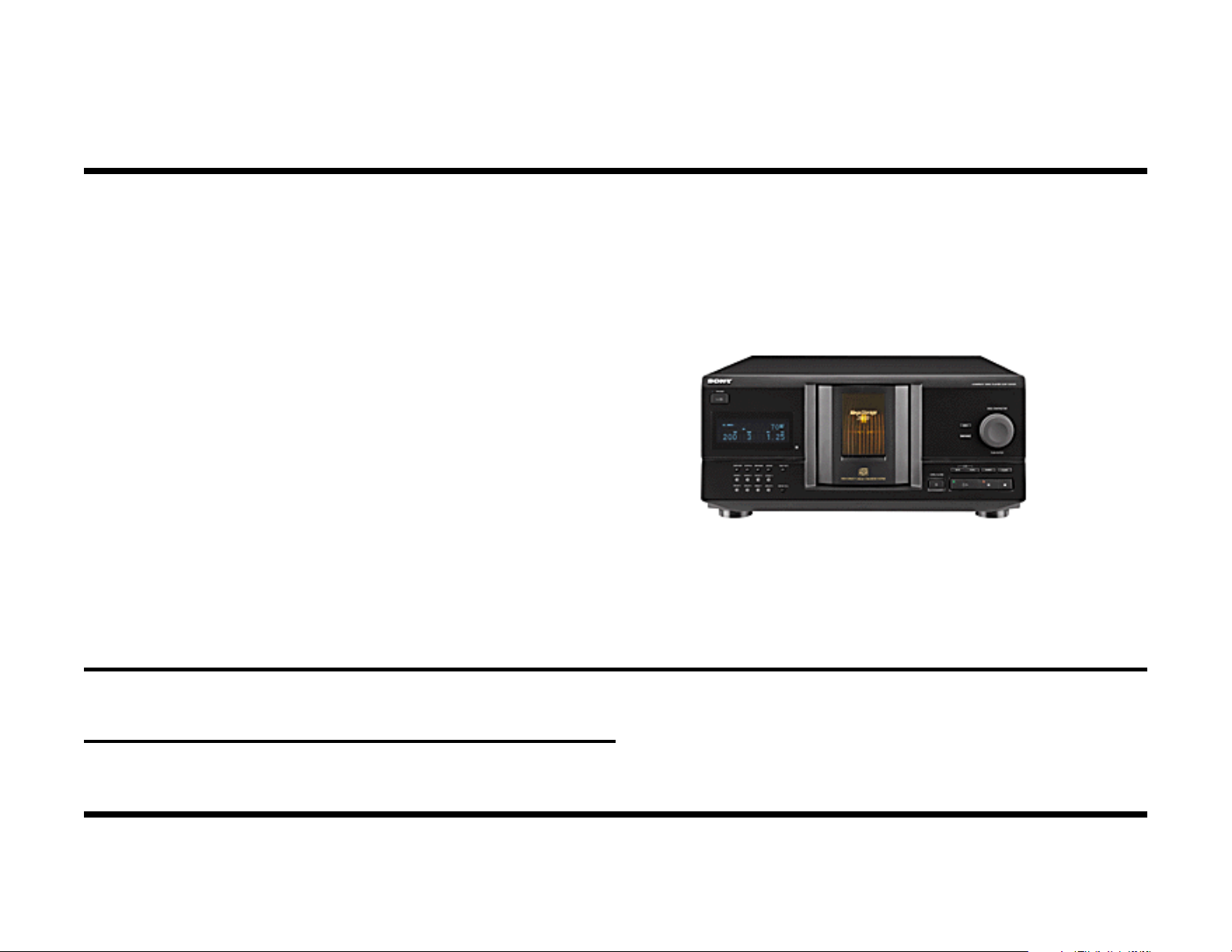
Model CDP-CX235
The board layout of the CDP-CX235 is shown. The bulk of the electronics
are on the rear main board. To its left in the vacant area is the CD mechanism housing the optical assembly and servo (BD) board. The small boards
along the bottom of the chassis hold the tray table and disc sensors. The
top illumination board houses 3 LEDs to light the disc compartment when
the CD Changer is powered on.
The model CDP-CX90ES/CDPCX-270 was carried over from the 1998
year because it was the only chassis that had the following major features:
• A video output for an on-screen display using a TV.
• A front panel jack that permitted a computer keyboard to be plugged
in. This allowed the user to label or re-label each CD slot location
quickly using the keyboard instead of the slower remote control
.
2
Page 8

3
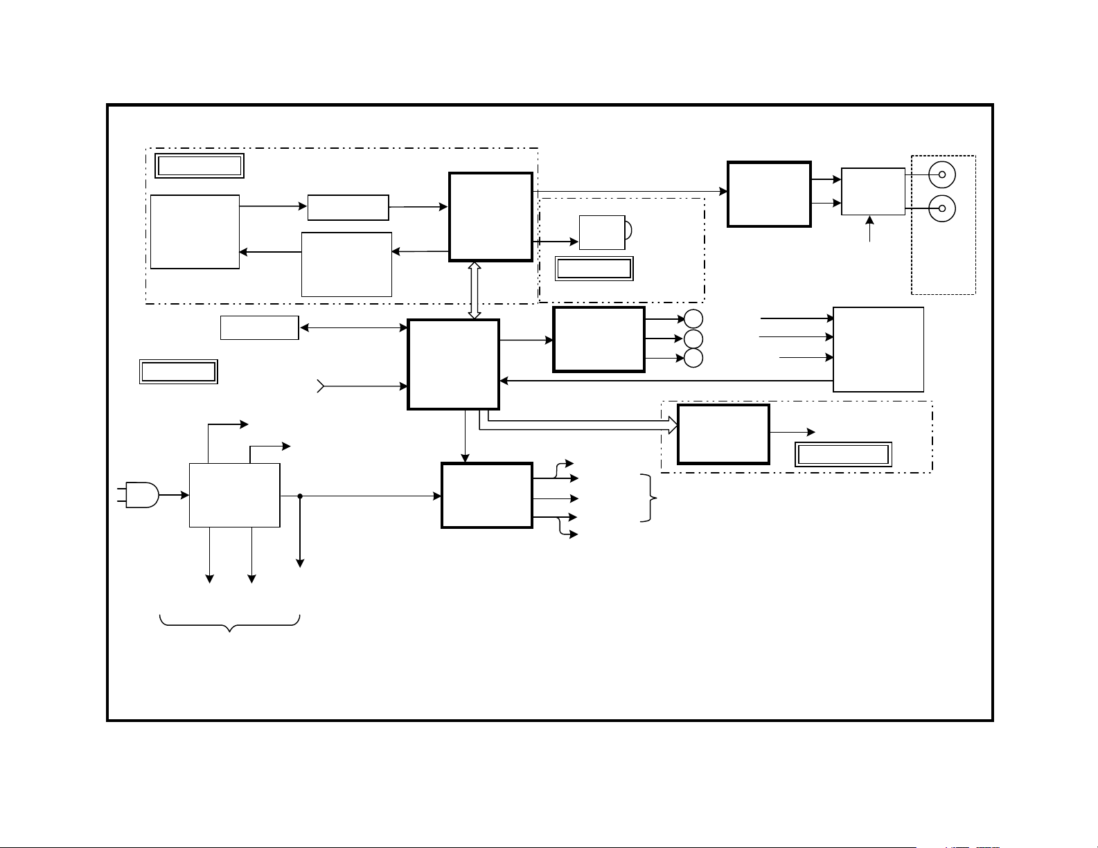
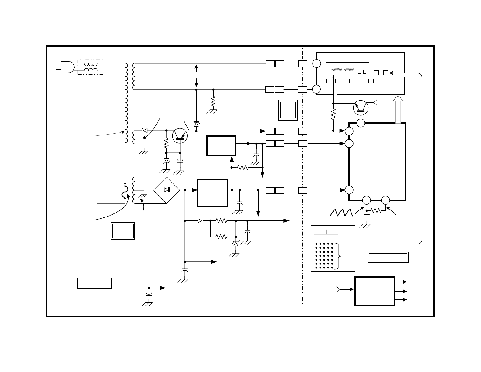
Overall Block Diagram
At the core of the 200 disc CD Changer is the System Control (Syscon)
IC501. IC501 serves as the interface between the user and the mechanism. Before IC501 can respond to the user’s commands for a disc to
play, it must know the following:
· If the Disc door is closed.
· If the CD Mechanism is in the chucked position.
· At which disc slot is the tray table is positioned.
Some of this information is stored in an external memory IC; the remainder IC501 will have to gather at power ON using the sensors and switches
linked to the Door, Tray Table and Loading Motors.
Information Gathering
Pressing the power ON button causes IC501 to use “IC SW” to switch on
regulator IC506. IC506 apples power to the BD board, which houses the
optical assembly. D+5V is also applied to the LED in the door compartment to inform the user power is ON.
After Syscon IC501 turns on power, IC501 accesses its external memory
IC. Data about the disc last loaded in the CD Mechanism is returned to
IC501. The disc label information is output as data to the FL Display IC
for display on the front panel fluorescent tube. If there was no label information, then just the disc’s number is displayed.
Syscon now takes a series of steps to check the memory information:
Once Syscon IC501 is confident the tray table information is valid, IC501
turns the CD Changer control over to the user by accepting pushbutton
commands.
The user can use the front panel controls to select another disc or play
that one. When Syscon knows the loading motor is in the chucked position (loading motor switch), the CD can be played.
CD Playback
Syscon IC501 initiates CD play by sending data, clock and latch communications to IC101 on the BD board. This causes IC101 to turn on the
laser, focus, tracking and spindle servos that employ the laser diode, along
with the focus coil, tracking coil, sled motor and spindle motor in the optical assembly.
Once these servos are operating, the disc information (RFO) is output.
RFO is received by Servo Control IC101 which:
• Converts the data back to the original modulation scheme (EFM).
• Error corrects the data (parity error correction).
• Reconstructs its original pattern (CIRC).
• Creates additional digital samples (oversampling) to reduce noise in
the final analog audio.
• Converts the signal from digital to analog form (D/A Converter).
1. Syscon activates the disc door motor to close the door if its corresponding switch indicates the door is open.
2. Next, Syscon checks the loading motor switch position to see if the
CD Mechanism is in the chucked position (disc loaded).
• If chucked, IC501 will initiate disc PB to read its TOC.
• If unchucked, IC501 will drive the tray table motor, rotating its discs
past the disc sensors. While the tray is rotating, the tray sensors
inform IC501 of the disc slot location while the disc sensor tells
IC501 if there is a disc present at that slot. The last disc played
according to memory will be loaded and its TOC read (if present).
Analog audio is output from IC101 to the rear panel jacks.
Page 9
BD BOARD
OPTICAL
PICK-UP
ASSEMBLY
KSS213B
MAIN BD.
-28V
SOURCE
MEMORY
POWER
SUPPLY
FILAMENT
VOLTAGE
A-F
RF AMP
COIL &
MOTOR
DRIVER
FRONT
PANEL
BUTTONS
-13.5V SOURCE
+5V SOURCE
+11.5V
SOURCE
RFO
ERROR
SIGNAL
IC501
SYSTEM
CONTROL
IC101
SERVO
CONTROL/
DSP
IC
SW
IC506REG
/SW
LINE OUT
D
OUT
DIGITAL
OPTICAL
OUTPUT
JACK BD.
IC503
MOTOR
DRIVER
FL DATA,CLK,LATCH
DISC DOOR
LIGHT
D+5V
+7V
RESET
AUDIO
MUTE
M
DOOR
M
TRAY
M
LOADING
IC701
FL DISPLAY
DRIVER
TO BD BOARD
IC401
AUDIO
AMP
MUTE
RESET
FROM
IC506
SWITCH OR
SENSOR
FL DISPLAY
TUBE
DISPLAY BD.
L
R
AUDIO
OUTPUT
(JACK
BD.)
TO DISPLAY BD.
OVERALL BLOCK DIAGRAM (MODEL CDP-CX235)
4
0A122 1251
7/5/00
Page 10

5
Power Supply / Display
Overview
The power supply stage produces seven voltages when the CD Changer
is plugged into AC. Some of these voltages from the main board power
the FL Driver microprocessor IC701 and the FL indicator tube on the display board.
Power Supply
Power Supply Output
Output Voltage From Destination
1. +11.5Vdc Bridge Rectifier
D501-4
2. 13.5Vdc Bridge Rectifier
D501-4
3. +5Vdc Source Regulator IC504 Syscon IC501 (not shown),
4. +5Vdc Bridge D501-4 &
Zener D508
5. Reset +5V Reset IC505 Syscon IC501 (not shown),
6. 3.7Vac Power Transformer
T901
7. -28V Q501/emitter Reference voltage for the
Regulator/Sw IC506,
+5V Regulator IC504,
Motor Driver IC503.
Audio mute transistors
(Q325/e, Q327/e and
Q425/e), Motor driver
IC503.
FL Driver IC701.
Mute transistors Q325/e,
Q327/e and Q425/e.
FL Driver IC701,
LED Driver IC702 (not
shown).
Fluorescent Display Tube
filament
Fluorescent Display
The positive output of the bridge rectifier is filtered by C501 to become the
+11.5V source voltage.
The negative output of the bridge rectifier is filtered by C502 to become
the –13.5V source voltage.
+5Volt Source
The +11.5V source voltage is reduced and regulated by IC504 to produce
the +5V source voltage for the CD Changer.
+5Vdc
The +11.5V source voltage is reduced by R505 and R508 and applied to
5.1 volt zener diode D508 for shunt regulation. Shunt regulation is when
a device like this variable resistance zener diode is placed in parallel with
the load. The zener diode resistance varies to keep the voltage at the
load reasonably stable.
This +5 volts that is output is used by the mute transistors Q325, Q327,
and Q425 to control the left and right channel audio muting at power ON
and OFF and when plugged and unplugged from AC.
D509 and C505 are used to insure there is sufficient voltage for the mute
operation when the unit is unplugged. C505 holds the +5V for the mute
transistors and diode D509 blocks this voltage from being used by the
loads on the 11.5V line (D509/anode).
Reset +5V
When the +5Volt Source voltage outputs regulator IC504, IC505 creates
a reset pulse using R506 and C507. Each one of these three parts has a
role in creating the reset pulse. When the source voltage is input IC505,
IC505 holds it output LOW for a fixed amount of time dependent upon
IC505’s design. This LOW grounds out C507 at the output. When the
IC505 releases ground, C507 is charged by R506 to +5V.
The reset output of IC505 is applied to the IC501 and IC701 microprocessors in this CD Changer. Generally, reset occurs when the reset input to
a device is held LOW while power (Vcc) is applied.
+11.5V Source / -13.5V Source
When the CD Changer is plugged into AC, this voltage is applied to the
primary winding of T901. The secondary winding that is center taped
applies 20.6Vac to a four-diode bridge rectifier designated D501 to D504.
Page 11

L901
NOISE
FILTER
CHOKE
Ω
55
THERMAL
FUSE
MAIN BD.
T901
JACK
BD.
C502
1000
2Ω
D505
Ω
2
Ω
2
+
41
R502
D506
30V
3.7VAC
FILAMENT
VOLTAGE
R501
33k
Ω
-28V
-40V
P
Q501
D507
6.2V
IC505
PST994D
C503
100
+
IC504
REG
TA7805
+
D501-
D504
D509
R505
R508
D508
5.1V
+11.5V SOURCE TO: IC506
REGULATOR,
IC503 MOTOR DRIVER
+
+11.5V
C501
3300
-13.5V SOURCE TO: MUTE
TRANSISTORS Q325,Q327,
Q425 AND IC503 MOTOR DRIVER
C507
R506
SYSCON
IC501/30
C506
C505
+
14 2 3
15 1 1
JOG
BD.
13 3 2
115
+
7 9 9
+5V
SOURCE
(B+)
+5V TO MUTE
TRANSISTORS
Q325/E,Q327/E,
Q425/E
FL701 FL INDICATOR TUBE
1
-28V
65
R701
100k
-28V
7
RESET
+5V
+5V
2.5V p-p
OSC.2.48MHz
WORDS
GRIDS 1-15
DATA,
CLK FROM
SYSCON IC501
G16
N
Q701
55
56
VFL
60
FL DRIVER
MSM9202-03GS
VCC
64
OSC0
C702
G
1
P
(36)
LED DRIVER
M66310FP
+5V
DIG 16
IC701
OSC1
58
59
R706
SQ. WAVE
DISPLAY BD.
IC702
P1-36
G1-15
5V p-p
FRONT
PANEL
LED’s
POWER SUPPLY (CDP-CX235)
6
1A122 1238
7/7/00
Page 12
7
When the output of IC505 is LOW, these microprocessors are held in
reset and are inactive (apparently dead).
3.7Vac
A low AC voltage from power transformer T901 is applied to the filament
of the fluorescent indicator tube FL701.
-28V
The 41-ohm secondary winding of transformer T901 produces 31.7Vac
that is rectified by D505. The –40Vdc produced is regulated by Q501
using zener diode D506 for voltage stabilization.
The –28Vdc output from regulator Q501/emitter is applied to the fluorescent driver stage as the negative supply voltage and to one end of the
filament via D507as the tube’s electron source.
Fluorescent Display
The FL701 Fluorescent Display tube needs the following to light a segment or a word in the tube:
• Filament voltage
• Positive voltage simultaneously applied to the grid and plate.
Basic Operation
The filament voltage comes from the power transformer T901 and the
positive pulses come from FL Driver IC701.
Just like a vacuum tube, the fluorescent display tube needs a source of
electrons. The electrons come from the filament, which is connected to
the –28V source. A controlling grid in the middle acts as a gate to determine if electrons should pass onto the plate to make it glow. At the gate,
a more positive voltage than the filament attracts the electrons and opens
the gate. A grid voltage that is the same as the filament will keep electrons from leaving the filament so there is no glow.
The plate structures will be phosphorescent when struck by electrons. To
get the electrons to the plate, the plate must have a positive voltage to be
attractive.
P1
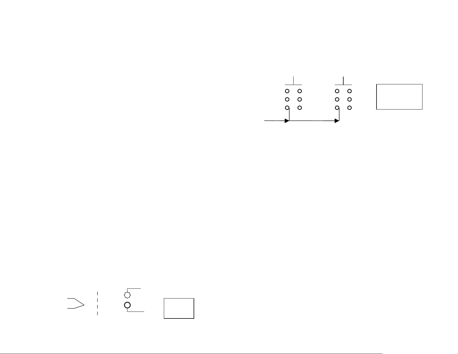
Grid & Plate Array
Within the FL tube there are 16 grid structures, each containing 36 plates.
Each grid structure produces a character or number by luminating a combination of plates.
P3
P1
P2
P3
G1
P4
P5
P6
P1
P2
P3
G2
P4
P5
P6
Plate and Grid
Structures
To make a specific plate glow, a grid structure is selected and a positive
voltage is applied to it. At that time, the plate structures that must glow
are also brought positive. In the diagram above, when G1 and P3 lines
are brought HIGH, the P3 plate in the G1 structure will glow. Even though
the P3 structure in the G2 structure is connected in parallel, receiving the
same voltage, it will not glow because the G2 voltage is LOW at this time.
The job of FL Driver IC701 is to create and time the grid and plate pulses.
Fluorescent Driver IC701
When the CD Changer is plugged into AC, Vcc is applied to IC701/pin 64,
starting its internal oscillator. The R-C parts that set the frequency of this
2.48MHz oscillator (16MHz is on the schematic) are located at IC701/
pins 58 and 59.
Also at AC plug in, the FL Driver IC701 is momentarily reset. IC505 momentarily holds its output LOW when +5V is input. This LOW resets FL
Driver IC701 when Vcc (power) is present at pin 64. The LOW lasts for
0.2ms (IC505) + 0.8ms (C507) = 10ms.
Simple FL
P2
GridFilament
Plates
Tube
Structure
Page 13

L901
NOISE
FILTER
CHOKE
Ω
55
THERMAL
FUSE
MAIN BD.
T901
JACK
BD.
C502
1000
2Ω
D505
Ω
2
Ω
2
+
41
R502
D506
30V
3.7VAC
FILAMENT
VOLTAGE
R501
33k
Ω
-28V
-40V
P
Q501
D507
6.2V
IC505
PST994D
C503
100
+
IC504
REG
TA7805
+
D501-
D504
D509
R505
R508
D508
5.1V
+11.5V SOURCE TO: IC506
REGULATOR,
IC503 MOTOR DRIVER
+
+11.5V
C501
3300
-13.5V SOURCE TO: MUTE
TRANSISTORS Q325,Q327,
Q425 AND IC503 MOTOR DRIVER
C507
R506
SYSCON
IC501/30
C506
C505
+
14 2 3
15 1 1
JOG
BD.
13 3 2
115
+
7 9 9
+5V
SOURCE
(B+)
+5V TO MUTE
TRANSISTORS
Q325/E,Q327/E,
Q425/E
FL701 FL INDICATOR TUBE
1
-28V
65
R701
100k
-28V
7
RESET
+5V
+5V
2.5V p-p
OSC.2.48MHz
WORDS
GRIDS 1-15
DATA,
CLK FROM
SYSCON IC501
G16
N
Q701
55
56
VFL
60
FL DRIVER
MSM9202-03GS
VCC
64
OSC0
C702
G
1
P
(36)
LED DRIVER
M66310FP
+5V
DIG 16
IC701
OSC1
58
59
R706
SQ. WAVE
DISPLAY BD.
IC702
P1-36
G1-15
5V p-p
FRONT
PANEL
LED’s
POWER SUPPLY (CDP-CX235)
8
1A122 1238
7/7/00
Page 14
9
,
,
Plug into AC
+5V
T
1
2
CH1 5.00 V=
CH2!5.00 V= MT B10.0ms- 3.16dv ch1+
Reset
10msec/div
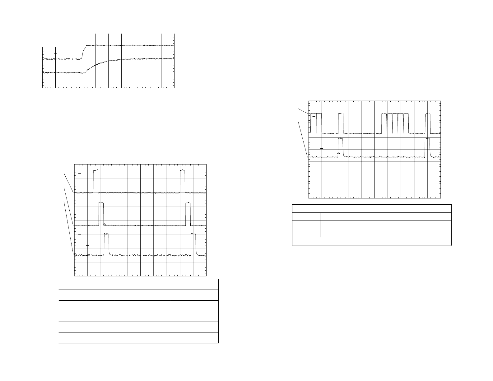
After reset, IC701 begins normal operation, producing sequential grid
pulses first. When IC701/pin 60 goes HIGH (+5V), IC701 outputs a positive going pulse at each grid pin, one after the other. Each grid pulse is
applied to a grid cluster consisting of 36 individual plate structures. After
all 16 grids are pulsed (G1 – G16), the sequence repeats. Nothing appears in the display at plug-in because the fluorescent tube has not received plate voltage.
The waveform below shows grid pulses applied to G14, G15, and G16 of
the fluorescent tube.
ch1
ch2
ch3
ch2:dc =-27.3 V, rms = 28.3 V
1
pkpk= 33.8 V, freq= 304 Hz
2
3
T
CH1 20.0 V=
CH2 20.0 V=
CH3!20.0 V= CHP MTB 500us- 2.34dv ch3+
Fluorescent tube Grid pulses at Power OFF
Plate voltage pulses appear only when the CD Changer is powered ON.
At power ON, Syscon (IC501 is not shown) sends data to IC701 so it can
output these pulses. Positive pulses are output the appropriate plate pins
P1-36 to form a number, letter or word when a grid pulse is simultaneously
present.
The following waveforms show a plate signal (Ch 1) compared to the grid
16 signal (Ch 3). This plate segment is lit at the grid assembly 16 location
when both the plate and the grid outputs are HIGH.
ch1
ch3
1
3
T
CH1 20.0 V=
CH3!20.0 V= CHP MTB 500us- 2.34dv ch3+
Fluorescent tube pulses during Power ON
Chan Name Location Voltage
1 P14 IC701/pin 18 30Vp-p
3 G16 IC701/pin 55 30Vp-p
Time base = 500usec
By looking at Channel 1, we see that the plate signal also goes high at
times when grid 16 is not HIGH (Ch 3 = LOW). This means a similar plate
at a different grid is lit at this time.
Chan Name Location Voltage
1 G14 IC701/pin 53 30Vp-p
2 G15 IC701/pin 54 30Vp-p
3 G16 IC701/pin 55 30Vp-p
Time base = 500usec
Page 15
L901
NOISE
FILTER
CHOKE
Ω
55
THERMAL
FUSE
MAIN BD.
T901
JACK
BD.
C502
1000
2Ω
D505
Ω
2
Ω
2
+
41
R502
D506
30V
3.7VAC
FILAMENT
VOLTAGE
R501
33k
Ω
-28V
-40V
P
Q501
D507
6.2V
IC505
PST994D
C503
100
+
IC504
REG
TA7805
+
D501-
D504
D509
R505
R508
D508
5.1V
+11.5V SOURCE TO: IC506
REGULATOR,
IC503 MOTOR DRIVER
+
+11.5V
C501
3300
-13.5V SOURCE TO: MUTE
TRANSISTORS Q325,Q327,
Q425 AND IC503 MOTOR DRIVER
C507
R506
SYSCON
IC501/30
C506
C505
+
14 2 3
15 1 1
JOG
BD.
13 3 2
115
+
7 9 9
+5V
SOURCE
(B+)
+5V TO MUTE
TRANSISTORS
Q325/E,Q327/E,
Q425/E
FL701 FL INDICATOR TUBE
1
-28V
65
R701
100k
-28V
7
RESET
+5V
+5V
2.5V p-p
OSC.2.48MHz
WORDS
GRIDS 1-15
DATA,
CLK FROM
SYSCON IC501
G16
N
Q701
55
56
VFL
60
FL DRIVER
MSM9202-03GS
VCC
64
OSC0
C702
G
1
P
(36)
LED DRIVER
M66310FP
+5V
DIG 16
IC701
OSC1
58
59
R706
SQ. WAVE
DISPLAY BD.
IC702
P1-36
G1-15
5V p-p
FRONT
PANEL
LED’s
POWER SUPPLY (CDP-CX235)
10
1A122 1238
7/7/00
Page 16
11
PM3394, FLUKE & PHILIPS
,
Power On
Once the CD Changer is plugged into AC, pressing the front panel Power
button permits Syscon to enable regulator IC506. IC506 outputs D+5V,
+7V, and a reset signal to power the remaining devices on the BD board
and turn on 2 LEDs to illuminate the disc door compartment.
AC Power Only
When the CD changer was plugged into AC, Syscon IC501 received power
at pin 37 and was fully functional as marked by the X501 activity at pins
31 and 32. There is even data and clock signals leaving IC501/pins 18,
19 and 58. These signals go to FL Display Driver IC701, but there is no
instruction to turn on the front panel display while the unit is still OFF.
ch1
ch2
ch3
1
T
2
3
pin 65 to enable regulator IC506. IC506 has three outputs:
1. D+5V from pin 2 is used to:
• Power the digital ICs on the DB board; and
• Turn on the LED at the disc door compartment. This also lets the user
know the unit is ON.
2. +7V from pin 9 is used to:
• Power the focus/sled/tracking driver IC102; and
• Power the coils and motors on the BD board
3. XRST from pin 6 goes HIGH to:
• Unmute the analog audio output lines; and
• Enable Servo Control IC101 and the focus/sled/tracking driver IC102
on the BD board.
Communications IC501 – IC701
At power On, the communications activity increases between IC501 and
IC701. This is to provide constant update information to the display IC701.
ch1
ch2
ch3
1
T
2
Power ON
Syscon IC501 receives the power ON command from the front panel push
button at pin 44 (LOW). IC501 responds by outputting a HIGH at IC SW
CH1 5.00 V=
IC501 Activity at Power OFF
Channel Name CN501/pin
1. FL Data 1
2. FL CLK (Clock) 2
3. FL LT (Latch) 4
Time base = 50usec/div
3
CH1 5.00 V=
IC501 Activity at Power ON
Channel Name CN501/pin
1. FL Data 1
2. FL CLK (Clock) 2
3. FL LT (Latch) 4
Time base = 50usec/div
Page 17
PUSH
BUTTONS
POWER
DISPLAY BD.
MAIN BD.
R732
CN701/602
+11.5V
+5V
2
JOG BD.
50mVp-p
X501
10MHz
4Vp-p
97
CN601/501
KEY 1
VCC
VCC
32
31
+5V
37 65
IC501
44
SYSCON
CXP84340-075Q
VCC
1
4
8
10
ICSW
IC506 LA5616
REG
EN1
EN2
REG
FL DATA
18
FL CLK
19
58
50
48
49
RESET
FL LT
DATA
CLK
XLT
DOOR
LUMINATION
C508
CN501
1
2
4
18
20
19
CN502
2
6
7
4.8V
9
+
IC701/PIN
63
62
61
5
7
6
IC101/PIN
D+5V
SOURCE
XRST TO
C509
IC101/3,
IC102/15
+5V
C511
+7V
SOURCE TO
DRIVER
IC102 (B BD.)
IC701
FL DRIVER
(DISPLAY BD.)
IC101
DSP
(BD.BD.)
TO
BD.
BOARD
POWER ON
MUTE
(MAIN BD.)
Q325,Q327,
Q425
POWER ON
12
2A122 1242
6 28 2000
Page 18
Communications IC501 – IC101
PM3394, FLUKE & PHILIPS
Communications from Syscon to Servo Control IC101 does not occur
until the disc is chucked on the spindle motor and ready to play (after the
loading motor finishes chucking the disc). This communications is shown
below:
ch1
13
ch2
ch3
1
2
T
3
CH1 5.00 V=
CH2!5.00 V=
CH3!5.00 V= CHP MTB1.00ms- 3.24dv ch3-
Channel Name CN502/pin
1. Data 18
2. CLK (Clock) 20
3. XLT (Latch) 19
Time base = 1msec/div
IC501 Activity at CD Play
Page 19

PUSH
BUTTONS
POWER
DISPLAY BD.
MAIN BD.
R732
CN701/602
+11.5V
+5V
2
JOG BD.
50mVp-p
X501
10MHz
4Vp-p
97
CN601/501
KEY 1
VCC
VCC
32
31
+5V
37 65
IC501
44
SYSCON
CXP84340-075Q
VCC
1
4
8
10
ICSW
IC506 LA5616
REG
EN1
EN2
REG
FL DATA
18
FL CLK
19
58
50
48
49
RESET
FL LT
DATA
CLK
XLT
DOOR
LUMINATION
C508
CN501
1
2
4
18
20
19
CN502
2
6
7
4.8V
9
+
IC701/PIN
63
62
61
5
7
6
IC101/PIN
D+5V
SOURCE
XRST TO
C509
IC101/3,
IC102/15
+5V
C511
+7V
SOURCE TO
DRIVER
IC102 (B BD.)
IC701
FL DRIVER
(DISPLAY BD.)
IC101
DSP
(BD.BD.)
TO
BD.
BOARD
POWER ON
MUTE
(MAIN BD.)
Q325,Q327,
Q425
POWER ON
14
2A122 1242
6 28 2000
Page 20

15
Door Motor Drive
The sliding door in the model CDP-CX235 was an improved feature over
the previous manual trap door that the user pulled down to access the
disc tray table. The sliding door mechanism consists of a motor that
drives a series of gears to slide the door on plastic tracks. The door motor
stops turning when the limit switch is toggled in the closed or open position.
Operation
Syscon IC501 controls the door movement. Only after the CD Changer is
powered ON will IC501 respond to the OPEN/CLOSE Door button at the
Key 2 input (IC501/pin 43).
Pressing the door button causes IC501 to check the position of the door.
S810, a 3-position switch, places one of three voltages at Syscon IC501/
pin 39 to indicate the door position.
Door Position Feedback
Door Position Location Voltage
Closed CN504/pin 1 2.5V
Neutral (in-between) CN504/pin 1 5V
Open CN504/pin 1 0V
A closed door will be driven open and vice versa.
Drive
Syscon IC501 applies an output voltage to pin 23 or pin 24 to drive the
motor. The resultant positive or negative voltage is applied to the door
motor.
Door Motor Drive
Movement IC501/pin 24 IC501/pin 23 IC503/pin 9
Door Opening 4.7V 0V -3.6V
Door Closing 0V 4.8V +3.7V
Feedback
As the door moves, S810 enters the neutral position and 5V is applied to
IC501/pin 39. When the door reaches the end of travel the door toggles
the S810 limit switch to the other end. IC501/pin 39 is lowered to either
2.5 or 0V. IC501 responds by stopping the motor voltage at pin 23 or 24
Page 21
S621
OPEN/
CLOSE
DOOR
+5V
CN601/501
JOG
BD.
R620
6
4
10
12
+5V
72
IC501
SYSCON
CXP84340
KEY 2
43 39
C620
73
DR
OUT
DR
IN
DOOR
SW.
24
23
R543
R552
R551
R553
8
7
(-VCC)
R554
12
-
+
CXA1291P 1/3
13 14
-13.5V
+11.5V
(VCC)
IC503
R555
1.2
9
Ω
DR-SW.
C551
R557
OUT 3
C552
R556
1.2
D OUT
R558
D IN
Ω
GND
CN504/811
CN812/810
3
4
2
1
1 2
DOOR
MOTOR BD.
M
M810
+5V
DOOR MOTOR DRIVE
16
R807
DOOR
SW BD.
OPEN
NEUTRAL
CLOSE
S810
3A122 1243
6 28 2000
Page 22

17
Tray Table Positioning
In order for the tray table to be positioned, two rows of slots are molded
into the bottom of the rotating tray table forming rings. These slots mate
with light sensors stationed on the bottom of the CD Changer. The sensors feed back information to Syscon so it can determine the exact tray
table position.
Tray Table Slots
At the bottom of the tray table, outer ring (#2) contains 200 equally spaced
slots that look like teeth. Each slot consists of an empty area (gap) in the
plastic ring that passes light and an equal width tooth that blocks the light.
One ring #2 slot corresponds to one disc slot.
Inner ring (#1) contains different spaced gaps. Ring 1’s smallest gap is
equal in width to one slot and one tooth pair in ring 2. Ring 1’s largest gap
is the width of ten of ring 2’s slots and teeth (10 disc slots). Generally, the
width of a gap is one for each group of 10 disc slots.
Light Sensors
Each light interrupt sensor forms a U channel. At one side of the sensor
there is an infrared LED that shines light through the channel. At the
other end is a phototransistor that monitors this light. When light passes
through the channel (light is received by the phototransistor), the electrical output is HIGH. When the channel is blocked, there is no electrical
output.
All three sensors are used to locate the tray position as the tray rotates.
Sensor IC801 monitors the gaps in ring #1. Sensors IC802 and IC803
are both used to monitor the gaps in ring #2. IC802 and IC803 sensors
are positioned off center to determine the center of the slot. This off
center information is necessary so the tray can stop the CD exactly in
front of the CD Mechanism each time.
IC801’s sensor records Ring #1’s gap width. These gaps increase as the
number of disc slots increase. Therefore with a minimum rotation of the
tray table, the home position can be calculated using the data from IC801
and one of the slot sensors like IC802.
Page 23

TABLE
RING 1
RING 1
RING 2
TABLE BOTTOM VIEW
IR
LED
SENSORS ON
T.SEN BD.
(TOP VIEW)
LIGHT INTERRUPT
SENSOR
IC801
IC802 IC803
PHOTO
TRANSISTOR
(OUTPUT IS
HIGH WHEN
LIGHT IS
RECEIVED)
RING 1
RING 2
TRAY TOP
RING 2
1
SLOT
2
SLOTS
10 SLOTS
(MAXIMUM)
TRAY TABLE POSITIONING
18
TRAY TOP
5A122 1246
6/29/00
Page 24

19
Table Motor Drive
Syscon IC501 drives the Disc’s Tray Table. IC501 receives information
from three tray table position sensors and the front panel rotary encoder
knob to determine where the tray is and where to stop.
Front Panel Rotary Encoder
Operation
At the front panel there is a large knob that is used to select discs. The
knob is connected to a rotary encoder switch on the jog board behind the
knob. When the knob is turned to the next detent position, the display
shows the information on the next disc in the tray. If that disc is desired,
the same encoder button is pressed (“Enter”) and that disc is accessed.
When the disc door is open, the rotary encoder rotates the tray to any disc
slot position, permitting the user to load discs. The FL display tube displays the same disc slot number marked on the tray at the opened door.
With the door closed, the display tube shows the disc slot facing the CD
Mechanism.
Display
Front
Panel
Door
The rotary encoder switch is connected to Syscon at
IC501/pins 42 and 43 respectively. At the encoder
itself there are three contacts for the rotary encoder
and two for the enter button. In the detent position,
pin 1 is connected to pin 2 (ground). In the neutral
position (in-between detents), pin 3 is connected to
pin 2.
Rotary
Encoder
knob
Rotary
Encoder
rear view
3 2 1
Direction of Rotation
The encoder is constructed so its direction from the detent position can
be determined by IC501. In the detent position, pin 1 is grounded. In the
neutral position, pin 3 is grounded. When turning the encoder knob in the
CCW direction, both pins 1 and 3 are momentarily grounded before pin 1
is ungrounded (“make before break”) in neutral. When turning the encoder knob CW, both pins 1 and 3 are open circuited before pin 3 is
grounded in neutral. This is how IC501 determines the direction the user
has turned the knob and rotates the tray accordingly.
Tray Table Position Sensors
Three sensors monitor the gaps in the tray table’s rings to determine home
position. Sensors IC802 and IC803 are used to determine the center of
each disc slot. Sensors IC801 and the composite signal from IC802 and
IC803 are used to determine where the tray is positioned.
For testing purposes, when the tray table is in a detent position, sensors
IC802 and IC803 should output a HIGH at CN506/pins 1 and 2. Sensor
IC801 outputs a HIGH when certain disc slot positions have been selected. The chart lists the disc positions IC801 will output a high in the
current 200 disc changers.
With the door open, you can rotate rotary encoder and verify the disc
positions in case the chassis has been bent or incorrectly aligned.
Disc positions when IC801 Output = HIGH (CN506/4)
Disc Positions
(# displayed on the tray)
10-18 8
30-39 9
50-60 10
70-71 1
90-92 2
110-113 3
130-134 4
150-155 5
170-176 6
190-197 7
Number of disc slots
Page 25

MEMO SEARCH
R624
ROTARY
ENCODER
RE601
R619
47k
S623
R625
1
DETECT
4
5
2
WIPER
3
NEUTRAL
INPUT
S622
DOOR
S621
R622
N=NEUTRAL POSITION
D=DETENT POSITION
R = 30.48k
T
Ω
KEY 2
CN601/501
KEY 3
6 7
6
5 11
MAIN BD.
KEY 3
42 43
IC501
SYSCON
CXP84340
TBLL
TBLR
TS3
64 63 62
3
4
TABLE
RING 1
TS2
2
TS1
5
TABLE
RING 2
CN807/507
R564
21
R562
22
R561
1
6
TABLE
RING 3
MOTOR BD.
1
R565
R563
5
6
+5V
5
6
1
2
TABLE TRAY
M
M801
R566
R567
-
+
CXA1291P 2/3
CN506/801
MOTOR
4
IC503
2
INTERRUPT
SENSOR
LOCATIONS
TOP VIEW
IC801
RING 1
JOG BD.
FRONT PANEL
DISC PB BUTTONS
S611-S617
R612-R618
RE601 KEY 3 KEY 2
DETENT 4.93 1.57
NEUTRAL 4.53 4.93
VOLTAGE
IC801 IC803 IC802
R803
R801
IC802
FLAG
IC802
HOME
R802
IC803
FLAG
T SENS BD.
TABLE MOTOR DRIVE
20
+5V
RING 1
RING 2
TABLE
BOTTOM
IC802
T.SEN BD.
IC803
4A122 1244
RING 2
7/5/00
Page 26

Tray Table Motor Drive
Syscon IC501 drives the motor that rotates the tray table. The following
voltages output IC501 and IC503 to move the table in the direction viewed
from the top.
Tray Table Drive Voltages
IC501/pin IC503/pinTable
Movement
Stop00000
CW 0 3.27 0.44 .45 5.37
CCW 3.27 0 0.044 0.042 -5.22
21 22 6 5 4
21
Page 27

MEMO SEARCH
R624
ROTARY
ENCODER
RE601
R619
47k
S623
R625
1
DETECT
4
5
2
WIPER
3
NEUTRAL
INPUT
S622
DOOR
S621
R622
N=NEUTRAL POSITION
D=DETENT POSITION
R = 30.48k
T
Ω
KEY 2
CN601/501
KEY 3
6 7
6
5 11
MAIN BD.
KEY 3
42 43
IC501
SYSCON
CXP84340
TBLL
TBLR
TS3
64 63 62
3
4
TABLE
RING 1
TS2
2
TS1
5
TABLE
RING 2
CN807/507
R564
21
R562
22
R561
1
6
TABLE
RING 3
MOTOR BD.
1
R565
R563
5
6
+5V
5
6
1
2
TABLE TRAY
M
M801
R566
R567
-
+
CXA1291P 2/3
CN506/801
MOTOR
4
IC503
2
INTERRUPT
SENSOR
LOCATIONS
TOP VIEW
IC801
RING 1
JOG BD.
FRONT PANEL
DISC PB BUTTONS
S611-S617
R612-R618
RE601 KEY 3 KEY 2
DETENT 4.93 1.57
NEUTRAL 4.53 4.93
VOLTAGE
IC801 IC803 IC802
R803
R801
IC802
FLAG
IC802
HOME
R802
IC803
FLAG
T SENS BD.
TABLE MOTOR DRIVE
22
+5V
RING 1
RING 2
TABLE
BOTTOM
IC802
T.SEN BD.
IC803
4A122 1244
RING 2
7/5/00
Page 28

23
PM3394, FLUKE & PHILIPS
CD Allocation & Label Storage
Syscon IC501 has its built-in memory to remember if the door was open
or closed, whether the disc was chucked or unchucked, and what order of
songs to play (program play). This information is lost when the CD Changer
is turned OFF. For other items that have to be remembered, IC501 uses
an external static (S-RAM) memory IC502, powered by C522 when the
changer is OFF.
IC502 stores the following information:
• Keeps track of what tray table slots have discs
• Stores disc slot number currently in use
• Groups discs (maximum of eight discs per group)
• Stores a name for each disc (Label)
• Logs tracks on a disc to be skipped (not played)
S-RAM Operation
IC502 is an S-Ram that stores bits of data using low power CMOS logic
gates. A one-Farad capacitor, C522, provides power to IC502 when the
CD Changer is turned OFF, preventing the loss of data for up to a month.
When the CD Changer is ON, Syscon IC501 can read or write into each
location of the memory by first enabling IC502 (CE = LOW), addressing a
memory location, selecting read (WE = HIGH) or write (WE = LOW), and
finally reading or writing the information. This S-RAM stores the information 8 bits at a time so a single address location reads or writes a Byte of
data (8 bits).
Writing to Memory
The memory writing operation can be seen in the first scope shot. It was
taken as the disc door is closing and the tray is rotating (press the Close
Door button). At this time, every disc slot is being checked for discs as
the tray rotates. If the memory information does not agree with the contents of the disc slot, the memory is rewritten to with the current information.
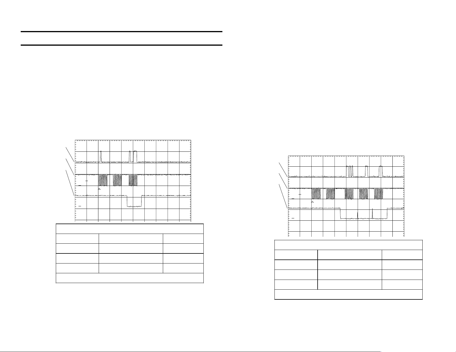
Channel 1 shows that S-RAM IC502 is enabled at power ON. Only one of
the 14 address lines is represented in channel 2. As the tray rotates,
IC501 sends its corresponding address to IC502.
ch1
ch2
ch3
ch4
1
2
T
3
CH1 5.00 V=
CH2!5.00 V=
4
CH3!5.00 V=
CH4!5.00 V= CHP MTB10.0ms- 1.66dv ch3-
Syscon Checking the Tray for Discs
Channel Name IC502/pin
1. CE (chip enable - low) 20
2. 1 of 14 Address lines 27
3. WE (write enable - low) 4
4. 1 of 8 Data lines 15
Time base = 10msec/div
At each address location, the data is read while the write enable line (WE
= Ch 3) is HIGH. This data (Ch 4) is sent to Syscon IC501 for comparison. Meanwhile, disc detector Q801 will place a HIGH at IC501/pin 38 if
there is NO disc at that slot location. If the memory also shows there is
NO disc at this location, the two pieces of information agree and there is
no change to the memory data. If they do not, WE goes LOW (Ch 3)
while still at that same address location (Ch 2) and the new data from
IC501/pin 38 is placed into memory.
Reading from Memory
The memory reading operation can be seen in the second scope shot.
This was taken with no disc chucked and the rotary encoder knob turned
to move the tray table. At each tray slot the memory location was read to
see if there is a disc at that slot.
Page 29

IC502
S-RAM
MSM5256DFP
CE
20
R521
28
VDD
A1-
A14
D0-
D7
Q521
INV
C522
1F 5.5V
1-9,
21,
23-
26
11-
13,
15-
19
27
WE
ADDRESS
DATA
R524
+5V
R522
68
R523
68
D521
112,
78-
80
7477,
68-
71
13
+5V
+5V
VDD
A0-
A14
IC501
SYSCON
CXP84340
D0-
D7
WE
14
72
CE
38
CN501/601
18
DATA
19
CLK
58
FLT
1 15
2
4
4
12
JOG
BD.
MAIN BD.
CN603/
702
4
5
6
63
FL DRIVER
62
61
G1-
G16
DISPLAY
DISP. BD.
IC701
MSM9202
P1-P36
FL
LUMINOUS BD.
D801
1
2
2
1
T.SEN BD.
R804
D. SEN BD.
Q801
2
1
1
2
324
5
+5V
CN80804/
CN802
CD LOCATION & LABEL STORAGE
24
DISC=LOW
NO DISC=HIGH
8A122 1248
7/5/00
Page 30

ch1
,
PM3394, FLUKE & PHILIPS
ch2
ch3
ch4
PM3394, FLUKE & PHILIPS
1
2
25
segments to display this information on the front panel display tube.
The following waveforms show the data, clock and latch signals from IC501
to IC701 used to produce a display when powered on.
ch1
ch2
ch3
1
3
CH1 5.00 V=
T
CH2!5.00 V=
4
CH3!5.00 V=
CH4!5.00 V= CHP MTB10.0ms ch4-
Reading the Tray Table Information
Channel Name IC502/pin
1. CE (chip enable - low) 20
2. 1 of 14 Address lines 4
3. WE (write enable - low) 27
4. 1 of 8 Data lines 15
Time base = 10msec/div
Note that the Read/Write channel 3 waveform remains HIGH, indicating
that only the memory reading operation takes place. Label and disc
availability data outputs as each tray table slot was addressed. In this
CD Changer example, there were no labels stored in memory so very
little data is present at channel 4.
Display Information
When the door is closed and the rotary encoder is turned, the memory is
checked for the next occupied slot location. As the tray moves the disc
toward the CD Mechanism, the label information is output. At each tray
slot location where there is a disc, the corresponding Label information
is sent to Syscon IC501. IC501 reorganizes the data and sends the
applicable information to the FL Display Driver IC701. If there was no
label information, only the disc number is sent. The Display IC assigns
2
T
3
CH1 5.00 V=
IC501- IC701 Communications (Power ON)
Channel Name IC501/pin
1. Data 1
2. Clock 2
3. Latch 4
Time base = 200msec/div
Oddly, even when the CD Changer is turned OFF, Syscon is sending
data, clock and latch signals into FL Driver IC701.
ch1
ch2
ch3
1
2
T
3
IC501- IC701 Communications (Power OFF)
Page 31

IC502
S-RAM
MSM5256DFP
CE
20
R521
28
VDD
A1-
A14
D0-
D7
Q521
INV
C522
1F 5.5V
1-9,
21,
23-
26
11-
13,
15-
19
27
WE
ADDRESS
DATA
R524
+5V
R522
68
R523
68
D521
112,
78-
80
7477,
68-
71
13
+5V
+5V
VDD
A0-
A14
IC501
SYSCON
CXP84340
D0-
D7
WE
14
72
CE
38
CN501/601
18
DATA
19
CLK
58
FLT
1 15
2
4
4
12
JOG
BD.
MAIN BD.
CN603/
702
4
5
6
63
FL DRIVER
62
61
G1-
G16
DISPLAY
DISP. BD.
IC701
MSM9202
P1-P36
FL
LUMINOUS BD.
D801
1
2
2
1
T.SEN BD.
R804
D. SEN BD.
Q801
2
1
1
2
324
5
+5V
CN80804/
CN802
CD LOCATION & LABEL STORAGE
26
DISC=LOW
NO DISC=HIGH
8A122 1248
7/5/00
Page 32

27
Disc Loading Drive
The purpose of the Disc Loading Drive stage is to rotate a cam that moves
levers to:
• Lock the tray table (after it has stopped)
• Grasp the disc from the tray table
• Guide the CD into the CD Mechanism
• Clamp the CD onto the spindle motor shaft (chucking)
• Release the CD when the cam reaches the end of travel.
Once the tray table has stopped, the Disc Loading Drive has the job of
getting the disc out of the tray table and placing it into the CD Mechanism
for play. From an electronic point of view, all that has to be done is to
rotate the Disc Loading Motor. The remainder is mechanical and is addressed in the overview and during alignment.
Operation
The electrical operation of this stage is similar to the Door Motor Drive.
After disc is placed on the tray table, Syscon IC501 positions the disc in
front of the CD Mechanism. The loading motor is powered to load the
disc into the CD Mechanism.
Loading Motor Drive Voltage
Cam Direction /
Function
CW / Chucking 3.1V 0V 3.4V
CCW / Unchucking 0V 3.1V -3.0V
IC501/pin 26 IC501/pin 27 IC503/pin 3
Motor Stop
Just before the cam reaches the end of travel, it toggles the S801 switch
on the L. SW Board. The switch grounds IC501/pin 55 or 67 depending
upon the direction of rotation. A LOW voltage instructs IC501 to discontinue the loading motor drive voltage. The loading motor stops.
Page 33

IC501
LDOT
SYSCON
CXP84340
IN SW
67 55
LDIN
OUT SW
27
26
R572
R571
R573
1.2
R567
IC503
CXA129IP 3/3
JACK
BD.
3
LD OUT
CN509/
902
1
CN902/808
1
M
M802
-
2
1
+
R574
2
R575
Ω
1.2
Ω
2
L. MOTOR BD.
+5V
R542
+5V
R541
MAIN BD.
OUT SW.
IN SW.
DISC LOADING DRIVE
28
CN505/806
S801
1
2
3
CAM CW
CHUCKED
NEUTRAL
CAM CCW
UNCHUCKED
L. SW. BD.
6A122 1247
6/29/00
Page 34

29
Optical Pickup
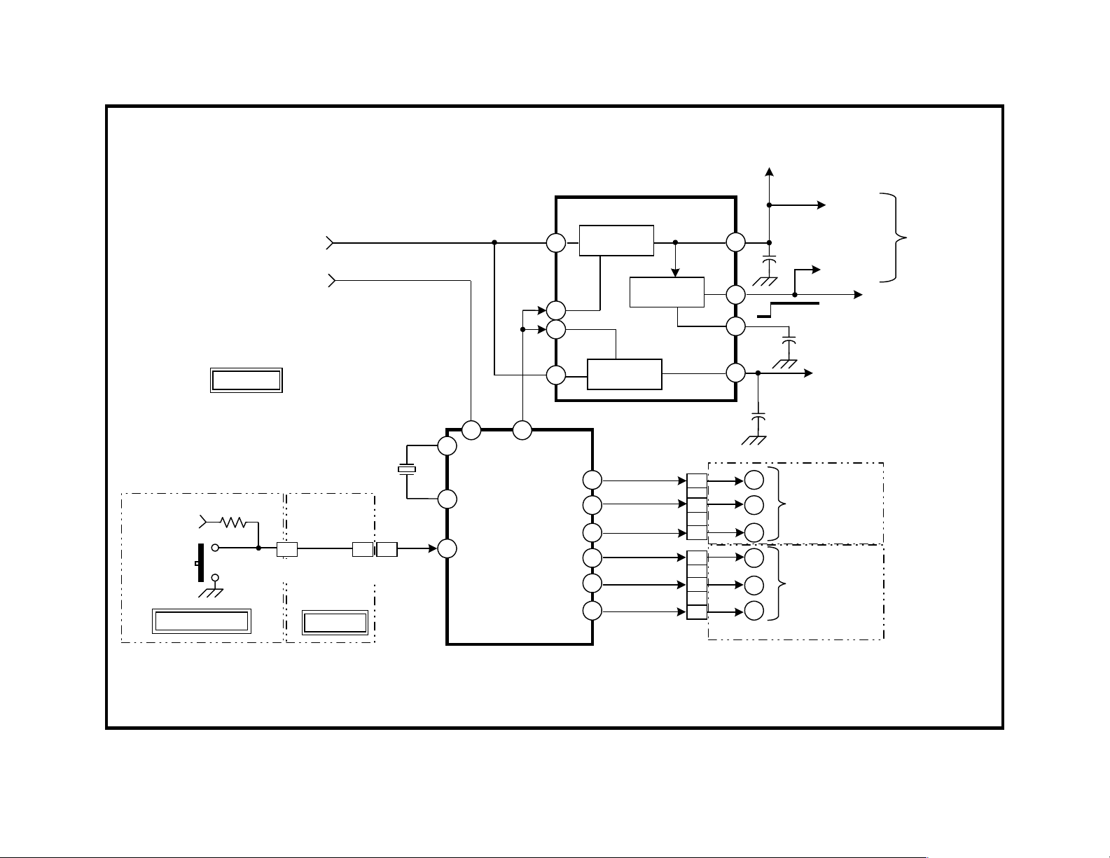
The Optical pick up assembly is the single most complicated device in the
CD player. The Optical assembly has several parts:
• The laser and objective lens
• Focus coil
• Tracking coil
• Detector assembly
Each part has a role in the playback of the disc information.
The Laser and Lens
The laser diode is powered by a regulated voltage (LD). Within the assembly is a photodiode that monitors the laser light intensity. This information (PD) is fed back to the circuitry to regulate the LD drive voltage.
The laser light is channeled through an objective lens towards the CD.
The convex objective lens funnels the laser beam into a focused point
near where the disc’s shiny information layer should be.
Focus Coil
The objective lens has a coil of wire attached to it in two planes. A stationary piece of metal is adjacent to it for magnetic reference. As current
flows through the focus coil, the lens is moved either toward or away from
the disc depending upon the direction of the current. Therefore, applying
sufficient current to this coil will move the lens and its focus point to the
disc’s information layer.
Detector Outputs
Laser light striking the information layer of the disc is modulated by the
data and returned to the detector area next to the laser diode. Detectors
A-F receive the light, amplify and output this signal to the external RF
amplifier to produce derived signals.
Optical Assembly Output Applications
Output Derived signal Purpose
Detectors A-D RFO (RF Output) Audio, Spindle
motor lock
Detectors A-D FE (focus error) Focus coil
correction signal
Detector E & F TE (tracking error) Tacking and sled
motor correction
signal
Tracking Coil
The tracking coil on the objective lens is perpendicular to the focus coil.
Current through this coil moves the lens and the laser beam to one side or
another. This movement keeps the laser beam on the spiral track as the
disc rotates. When the tracking coil has moved the lens to the limit, the
sled moves the optical assembly to follow the spiral track. This re-centers
the lens within limits and the tracking coil can continue to follow the track
once again.
Page 35

FOCUS
COIL
FOCAL
POINT
LENS
LASER
BEAM
CD
LASER
BEAM
TRACKING
COIL
TRACKING
ERROR
SIGNAL
FOCUS
ERROR
SIGNAL
(FE)
PD
LASER
CONTROL
OPTICAL PICKUP
LD
A-D,E,F
DETECTOR
OUTPUT
30
7A122 1245
7/7/00
Page 36

31
Servo / Audio Processing Block
In order for the CD player to produce audio, the servo section must control the laser beam so it can recover the digital data from the disc. Once
the data is stable and output at a constant rate, it can be processed and
returned to analog audio.
Servo Block
A chain of events must occur for the laser to read the disc’s data. The
sequence is as follows:
CD Play Sequence
Operation Purpose Check
1. Optical block
returns to home
position
2. Laser turns ON To read the disc
3. Focus search /
servo ON
4. Tracking servoONFollow the disc s
5. Spindle servo
ON
6. CD Data to
analog
conversion
When there is a break in the sequence, music cannot be recovered. Examining the waveform at test points can test each servo.
Begins reading the
CD at the TOC area
data
Find and maintain
focus on the disc
spiral information
track
Spin the disc so the
data is output at a
constant rate
Music recovery
(processing)
Sled moves the
block toward spindle
motor at Power ON
Laser power meter
Scope at the FOK
test point. Disc
spins after focus is
found.
Scope at the TE test
point
Disc spins. Lock
test point = HIGH
when data rate
controls the speed.
C2PO test point =
LOW when no
recovery errors.
Audio output
Sled Motor
When the CD Changer is turned ON (no disc chucked), the tray table
rotates to determine its position. Within the CD mechanism, the sled
motor drives the optical assembly toward the spindle motor until the limit
switch is closed. If this switch doesn’t close, the laser and focus search
will not take place and the CD will not spin.
Servo
Control
Focus Search
The focus operation is divided into search and servo parts. Servo Control
starts focus search when it knows the sled is at home position (S101) and
the CD Mechanism enters the chucked position (cam switch S801).
Servo Control makes a ramp voltage used to drive the objective lens
through its full length of travel, moving the distant focus point along with it.
S101
S801
Servo
Control
Driver
Limit switch S101
Driver
Focus coil in optical assembly
M
5V
focus
lens
Focus Servo
When the laser focuses on the disc’s reflective information layer, light is
returned to the optical assembly detectors. The A-D detectors are output
to the RF Amplifier. The RF stage not only amplifies the level but also
matrixes the signals to produce FE and RFO signals. FE is an output
signal used to identify and maintain focus when finally applied to the focus coil of the optical assembly. RFO is the main signal that will be
processed into audio if the servos all work.
Servo Control receives the FE signal and uses it with RFO to determine
when focus has been found during focus search. Focus is found when
the FOK (test point) goes HIGH. This is when Servo Control replaces the
Page 37

OPTICAL
PICKUP
ASSEMBLY
A-F
RF
AMP
COIL/MOTOR
DRIVE
LOADING SW. S801
(DISC CHUCKED)
USER
PUSH BUTTONS
LIMIT SW. S101
(OPTICS AT HOME
POSITION)
FE
DIG SIGNAL
PROCESS (DSP)
DATA
CLK
SYSCON
TE
SERVO
CONTROL/
CD
DATA
(SUB Q)
RF 0 (EYE PATTERN)
FOK
LOCK
C2PO
FL DISPLAY
DATA
CLOCK,
LATCH
ANALOG
AUDIO
OUT
DIGITAL
OUT
DISPLAY
TUBE
PLATE,GRIDS
DRIVER
SERVO/AUDIO PROCESS BLOCK
32
9A122 1251
6/29/00
Page 38

33
search voltage with an amplified FE voltage. The FEO output is sent to a
current driver IC. This IC drives the optical assembly’s focus coil to maintain focus on the disc during playback.
The FE and RFO waveforms can be used in troubleshooting to determine
if there is a signal output the optical assembly. The FOK test point can be
used to determine if the quality of the two signals is sufficient to find focus.
Tracking Servo
Once focus is found (FOK goes HIGH), the spindle motor starts and the
tracking servo loop is closed. The tracking servo moves the objective
lens so the laser can follow the disc’s information track.
The center of the disc’s track is identified using optical assembly detectors E & F. The RF Amp converts these two input signals into a tracking error (TE) correction signal that is sent to Servo Control. Servo
control amplifies the TE input and closes the servo loop switch, outputting the amplified tracking error signal (TEO).
Servo Control
RFO,
FE
TE
TEO
Driver
TE test point
The driver IC that receives TEO supplies current to generate a magnetic
field in the tracking coil. The coil moves the objective lens (with laser
beam) so the beam follows (tracks) the disc data.
Optical
Assembly
E, F
RF Amp
Spindle Motor
Like the focus serve, the spindle motor servo has two modes of operation.
As soon as focus is found, the spindle motor is kick started and runs to
approximately the correct speed. This is the first mode of the spindle
motor operation.
The second mode comes some time later after the tracking servo operates. This is when the RFO data is reliable and can be used to govern the
spindle motor speed. This second mode of operation cannot be seen
because the motor is already running. However when the motor is linked
to the disc data, the LOCK test point goes HIGH.
Lock
Spindle
Servo Control
RFO
FE
LPF
RF
Amp
A-D
Driver
Optical
Assembly
M
detectors
Audio Block
Once the spindle motor is locked to the data (LOCK = HIGH), the data is
reliable enough to be audio processed. The disc data comes into Servo
Control as RFO. It is error corrected, digitally reconstructed and output
as a digital signal to the rear panel jack. The digital signal is also converted to analog within Servo Control and delivered to the rear panel L &
R jacks.
While audio is output, the front panel display is receiving the CD track and
playback time information. Servo Control sends Sub Q digital data (and
clock) to Syscon for compiling and interpreting. The resultant information
is sent to the FL Display Driver as Data, Clock and Latch signals. The
Display driver determines what display segments of the tube have to be lit
to produce the desired time and track characters.
Page 39

OPTICAL
PICKUP
ASSEMBLY
A-F
RF
AMP
COIL/MOTOR
DRIVE
LOADING SW. S801
(DISC CHUCKED)
USER
PUSH BUTTONS
LIMIT SW. S101
(OPTICS AT HOME
POSITION)
FE
DIG SIGNAL
PROCESS (DSP)
DATA
CLK
SYSCON
TE
SERVO
CONTROL/
CD
DATA
(SUB Q)
RF 0 (EYE PATTERN)
FOK
LOCK
C2PO
FL DISPLAY
DATA
CLOCK,
LATCH
ANALOG
AUDIO
OUT
DIGITAL
OUT
DISPLAY
TUBE
PLATE,GRIDS
DRIVER
SERVO/AUDIO PROCESS BLOCK
34
9A122 1251
6/29/00
Page 40

35
PM3394, FLUKE & PHILIPS
Servo Processing
There are several main servos that can be tested for normal operation.
Sled Motor Drive
When the power On button is pressed, the sled motor is driven inward
until the optical assembly that is connected to it closes the S101 limit
switch. This closure places 5V at IC101/pin 27 so it may turn on the
servos to begin the disc playback sequence.
Laser
The Laser servo is the first to be turned on when the S101 limit switch is
closed and the loading switch is in the (disc) chucked position. IC101/pin
14 outputs a HIGH (5V) to RF Amp IC103/pin 22 to enable the laser servo.
The laser diode and light sampling photodiode are in the optical assembly
and the remainder of the regulating circuit is in IC103 with Q101 as an
external amplifier. IC103/pin 3 drops from 5V to about 3V to turn on the
laser. Q101 turns on, supplying current to the laser diode at pin 10 of the
optical pick-up ribbon cable connector. The laser diode will turn on when
there is sufficient current to drop about 1.8 to 2.2V at the diode.
Precautions
Although not recommended, if you must apply an external voltage to check
the diode, you must current limit this with a 1k-ohm resistor to prevent
laser diode damage. NEVER LOOK AT THE LASER DIODE LIGHT.
Use a laser power meter to measure the intensity of this class 1 laser.
Also, if your ohmmeter outputs more than 2V, do not check the laser
diode for diode continuity.
The laser intensity is monitored by a photo diode in the optical assembly.
The PD output into IC103/pin 4 is used to regulate the LD output from pin
3.
Laser Diode Control Voltages
Laser IC103/pin 3 Q101/Collector IC103/pin 4
OFF 4.76V 0V 0V
ON 3.17V 1.98V 0.116V
Focus
The focus search operation is also initiated when the disc is chucked in
the CD Mechanism (S801 not shown) and the limit switch (S101) is closed.
Servo Control IC101 generates the electrical signal that results in the
visible lens movement in the optical assembly.
The changeover from search to servo lock occurs when RFO signal is
present and the FE “S curve” shaped signal voltage crosses to/through
Vc voltage (half of Vcc. Vc = 2.5V). At this recognition time, FOK at
IC101/pin 24 goes HIGH to mark the transition to servo operation. If this
transition were inhibited so only the search operation took place, the RFO
and FE waveforms would look like this:
ch1
ch2
T
1
2
CH1 1.00 V= PKD
CH2!2.00 V= MTB2.00ms- 3.10dv ch1+
S Curve focus Search (Changer is in ADJust Test Mode)
Channel Signal Name Location
1 RFO test point IC103/pin 16
2 FE test point IC103/pin 14
Time base = 2msec/div
Scope ground is taken at Vc (IC103/pin 12)
Normally as the FE (Ch 2) signal would cross through Vc, IC101 would
start focus servo and the top half of the FE waveform (above the Vc base
line) would never take place.
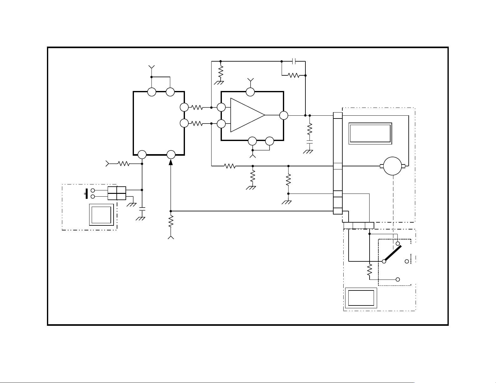
Page 41

D+5V
RIBBON
CABLE
CONNECTOR
CN102
+7V
OPTICAL
PICKUP
KSS-213B
FOCUS
COIL
13,16 14,15
VCC
21
22
VCC
8
VCC
VCC
TRACK
COIL
IC102
DRIVER
BA6382FP
2 24
1 12
5V
2.5V
DETECTOR
OUTPUTS
3-
8
10
A-F
Q101
12
FE
R103
FOCUS,TRACK
SLED DRIVE
LPF
X101
16.93MHz
R105
VCC
VC
IC103
RF AMP
CXA2568M
3
LD
4
PD
14 13 22 16
R101
39 41
TE
FE
MDP
26
67
66
27
6 57
L D ON
TE
14 43
RF
LD
ON
IC101
DSP, CLV
SERVO,
CXD2587 Q
19
RFO
RFDC
25 24
59
10
72
75
60
1
2
L OUT 1
L OUT 2
D OUT
SQS
SQCK
D+5V
L,R CH
AUDIO OUT
DIG OUT
SUB Q DATA
CLOCK TO
SYSCON IC501
MM
SPINDLE
SLED
HOME
S101
D+5V
XLT CLK
49 5048
IC501SYSCON (MAIN BD.)
SERVO PROCESSING
36
C2PO LOCK FOK
DATA
10A122 1249
6 28 2000
Page 42

37
339 , U & S
PM3394, FLUKE & PHILIPS
PM3394, FLUKE & PHILIPS
Tracking Servo
The tracking servo is turned on after focus is found (FOK = HIGH). This
servo results in a periodic track correction signal that looks like about
400mV of noise at the TE test point.
ch1
ch2
Channel Signal Name Location
1 RFO test point IC103/pin 16
2 TE test point IC103/pin 13
When the tracking loop is open, the laser is no longer following the data
track. In the following scope shot, the RFO waveform in channel 1 shows
the laser is seeing alternate areas of RF data (teeth) and no data (gaps).
Channel 2 shows there is TE correction signal generated from IC103/pin
13, but it is not reaching the tracking coil for correction.
ch1
ch2
ch1: pkpk= 1.44 V
1
2
CH1 1.00 V= STOP
CH2! 200mV= MTB1.00ms PKD ch1+
Normal CD Playback
Time base = 1msec/div
Scope ground is taken at Vc (IC103/pin 12)
ch1: pkpk= 1.28 V
1
2
CH1 1.00 V= STOP
CH2! 500mV= MTB1.00ms PKD ch1+
Defective Tracking Servo Waveforms
Channel Signal Name Location
1 RFO test point IC103/pin 16
2 TE test point IC103/pin 13
Time base = 100msec/div
Scope ground is taken at Vc (IC103/pin 12)
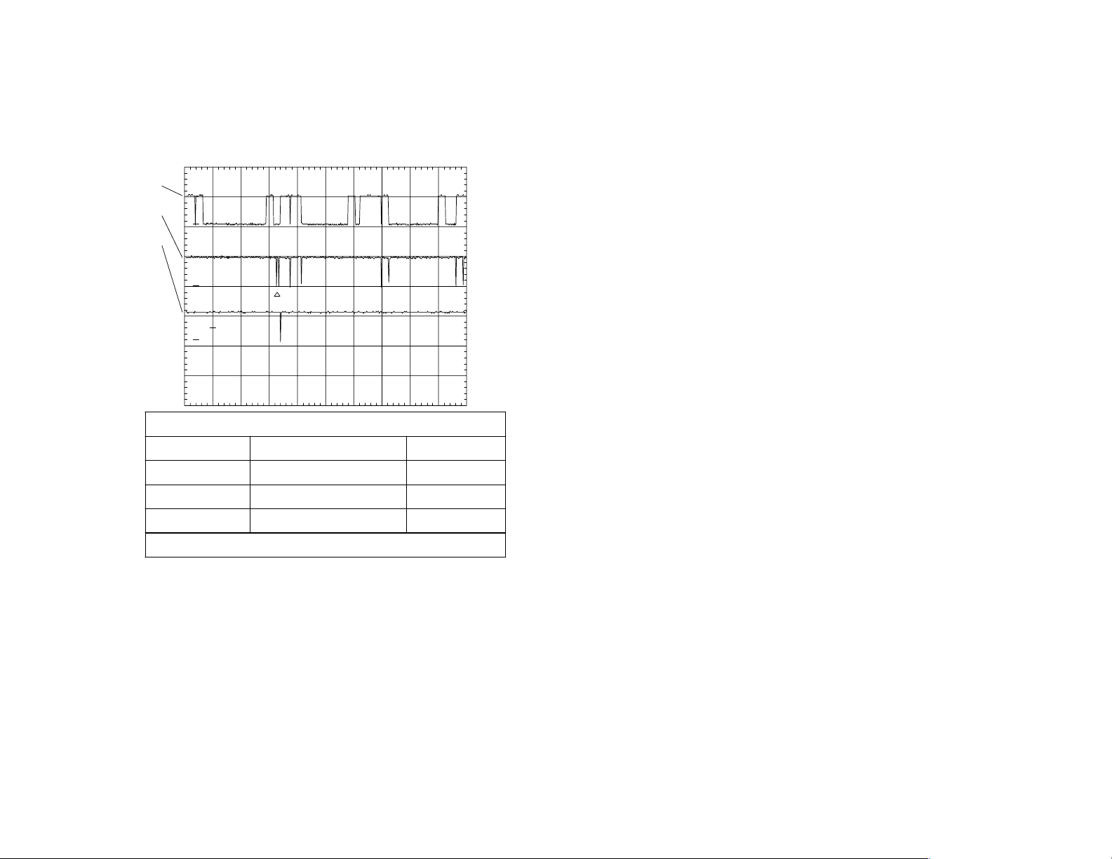
Spindle Servo
Although the spindle motor has started when focus was found (FOK =
HIGH), its lock onto the data does not occur until about 800msec later. At
that time the LOCK signal goes HIGH.
ch1
ch2
ch3
ch4
Channel Signal Name Location
1 RFO IC103/pin 16
2 FOK test point IC101/pin 24
3 LOCK test point IC101/pin 25
4 C2PO test point IC101/pin 19
At this time, the RFO signal should be at least 1Vp-p (1.2Vp-p = normal)
and the RFO waveform should be straight on top and bottom (no dropouts).
Once the LOCK test point goes HIGH, the servos are all working and
audio should output if that processing within IC101 is OK.
T
1
2
3
CH1 2.00 V=
CH2!5.00 V=
4
CH3!5.00 V=
CH4!5.00 V= CHP MTB 200ms- 2.28dv ch1+
CD Playback Starting
Time base = 200msec/div
Scope ground is taken at Vc (IC103/pin 12)
Page 43

D+5V
RIBBON
CABLE
CONNECTOR
CN102
+7V
OPTICAL
PICKUP
KSS-213B
FOCUS
COIL
13,16 14,15
VCC
21
22
VCC
8
VCC
VCC
TRACK
COIL
IC102
DRIVER
BA6382FP
2 24
1 12
5V
2.5V
DETECTOR
OUTPUTS
3-
8
10
A-F
Q101
12
FE
R103
FOCUS,TRACK
SLED DRIVE
LPF
X101
16.93MHz
R105
VCC
VC
IC103
RF AMP
CXA2568M
3
LD
4
PD
14 13 22 16
R101
39 41
TE
FE
MDP
26
67
66
27
6 57
L D ON
TE
14 43
RF
LD
ON
IC101
DSP, CLV
SERVO,
CXD2587 Q
19
RFO
RFDC
25 24
59
10
72
75
60
1
2
L OUT 1
L OUT 2
D OUT
SQS
SQCK
D+5V
L,R CH
AUDIO OUT
DIG OUT
SUB Q DATA
CLOCK TO
SYSCON IC501
MM
SPINDLE
SLED
HOME
S101
D+5V
XLT CLK
49 5048
IC501SYSCON (MAIN BD.)
SERVO PROCESSING
38
C2PO LOCK FOK
DATA
10A122 1249
6 28 2000
Page 44

39
PM3394, FLUKE & PHILIPS
Audio / Display Output
Analog Audio Output
The left and right channels of Servo Control IC101 are applied to amplifier
IC401. Their outputs are AC coupled to the rear panel phono jacks. The
following signal levels were measured using the Sony YEDS-18 test disc
track #5 (10kHz mono, 0db).
IC401 voltages
Measurement Pin 2 Pin 3 Pin 1
DC 0V 0V 0V
AC 3Vp-p 3Vp-p 5Vp-p
Muting transistors Q325, Q327, and Q425 mute the output audio at power
ON and OFF.
Digital Output
The digital output signal from Servo Control IC101/pin 60 is applied to
IC901 at the rear panel of the changer. Inside IC901 is a visible LED in a
plastic package that can connect to the consumer standard optical cable.
There is always a base waveform at the Digital Output pin 60 of IC101,
producing an average DC voltage of 2.47Vdc. This waveform keeps the
optical output LED lit (red) when the changer is powered ON.
When a disc is played, the base frequency square wave is replaced with
data.
T
1
Digital Output Signal Power ON, Disc PB
Name Location Frequency
Digital Output
(electrical)
CN502/pin 10 (from
IC101/pin 60)
data
Time base = 0.5usec/div
Display
SQ data and clock from Servo Control IC101/pins 1 and 2 are applied to
Syscon IC501 for processing. The results of this data will be the CD time,
track, and name information applied to the FL display driver IC701. The
SQ data and clock are only present when a disc is played.
ch1
ch2
T
1
T
1
Digital Output Signal Power ON, No PB
Name Location Frequency
Digital Output
(electrical)
CN502/pin 10 (from
IC101/pin 60)
1.4MHz
Time base = 0.5usec/div
2
CH1 2.00 V=
CH2!2.00 V= MTB10.0u s- 1.76dv c h1-
Disc PB track 1
Channel Name Location
1 SQSO / Sub Q CN502/pin 12
2 SQCK / SQCLK CN502/pin 14
Time Base = 10usec/div
Page 45

IC401 1/2
BA4558
LINE OUT 1
IC101/72
BD BD.
LINE OUT 2
IC101/75
DIGITAL OUT
IC101/60
SQ SQ
IC101/1
SQ CK
IC101/2
CN101/502
2
22
4
20
10
14
12
12
14
10
C301
+
R304
C401
R404
3
+
-
2
1
C305
+
L
TO AUDIO
OUTPUT
JACK J904
(JACK BD.)
R
R305
IC401 2/2
+
5
+
7
6
-
C405
+
MUTE
RST FROM
POWER ON
IC506/6
R405
TRANSISTORS
Q325
Q327
Q425
DIG OUT TO IC901
(JACK BD.)
52
SYSCON
51
CXP84340
IC501
18
19
58
DATA
CLK
XLT
IC701
FL DISPLAY
DRIVER
MAIN BD.
AUDIO/DISPLAY OUTPUT
40
11A122 1250
7/5/00
Page 46

41
OPTICAL
PICKUP
ASSEMBLY
COIL/MOTOR
DRIVE
USER
PUSH
BUTTONS
A-F
FE
DATA
CLK
RF
AMP
RF 0 (EYE PATTERN)
TE
SERVO
CONTROL/
DIG SOUND
PROCESS (DSP)
CD
DATA
(SUB Q)
SYSCON
DATA
CLOCK,
LATCH
SERVO/AUDIO PROCESS BLOCK
FOK
LOCK
C2PO
ANALOG
AUDIO
OUT
DIGITAL
OUT
DISPLAY
TUBE
FL DISPLAY
DRIVER
PLATE,GRIDS
9A122 1251
6/14/00
BD board - NewBD board - Old
Page 47

Troubleshooting
The CD Changer can be divided into two main areas: The Changer mechanism that selects the disc from the tray table and the CD disc Playback
mechanism that reads the track of information from the disc and produces audio.
The Changer mechanism periodically requires mechanical adjustment to
compensate for wear of parts over a time. This will make sure the correct
disc is identified and selected.
The Playback mechanism is more involved, requiring an understanding
of the playback details for efficient repair.
Failures in the playback mechanism can be classified into these symptoms:
• Disc doesn’t spin.
• Disc spins but doesn’t read the disc’s table of contents (TOC).
3. Press the POWER button and the optical assembly should return home.
(The tray table should also rotate at this time.)
When the optical assembly reaches home it should close the limit switch
and power to the sled motor will stop. The white gear should be free
(unpowered), proving the limit switch is OK. You can also test the limit
switch with an ohmmeter.
• No Audio.
Disc Doesn’t Spin
Before the disc spins, the sled must be at home position, the laser must
be turned on, and focus must be found. All of these things can be checked
easily.
Sled
In the CD Mechanism, you will manually move the optical assembly away
from home position. When you power up the CD changer, the sled motor
will turn, moving the optical assembly to the limit switch. This proves the
sled assembly is basically OK. As you move the gears make sure they
move without binding. The limit switch must be tested with an ohmmeter.
The sled check procedure is as follows:
1. Shut off power by pressing the POWER button if necessary.
2. Locate the large white gear in the CD Mechanism and rotate it so the
optical assembly moves
the home position).
away from the spindle motor shaft (which is
Laser
It is best to measure the laser brightness with the Leader model 8001
laser power meter. During focus search, the laser power is 0.03mW in
this model CDP-CX235 200 disc CD changer. The procedure is:
1. Remove the magnet assembly by pulling it outward at a 2 o’clock
direction.
42
Page 48

43
WON’T SPIN
SENSORS
SWITCHES
SLED
OK
REPAIR OR REPLACE
DEFECTIVE
COMPONENT
NG
CHECK
SPINDLE
CLV MOTOR
DRIVE
OK
HIGH PROBABILITY
OF BAD PICK UP
CHECK
CIRCUIT
NG
OK
NG
CHECK
DISPLAY
CHECK SLED
LIMIT SWITCH
OK
CHECK
FOCUS (FOK)
VOLTAGE
NG
CHECK
FOCUS LENS
MOVEMENT
OK
CHECK FOR
LASER LIGHT
NG
NG
NG
LIGHT
REPAIR
REPAIR
FOCUS
SERVO
CHECK SLED
SWITCH
OK
CHECK
POWER
SUPPLY
NG
REPAIR
P.S.
NG
OK
CHECK
SYSCON/FL
DRIVER
REPAIR OR REPLACE
DEFECTIVE
COMPONENT
REPLACE
PICK UP
REPAIR
APC CIRCUIT
DISC WON’T SPIN FLOW CHART
HIGH
PROBABILITY OF
BAD PICK UP
12A122
7/5/00
Page 49

2. Without CDs in the tray table, momentarily place your fingers between
the disc tray and the luminous sensor as you turn the power on. The
changer will mistakenly sense many discs, attempt to load them and
turn on the laser.
2. On the main board, connect the “ADJ” test point to ground. In the
CDP-CX235,
negative lead of the large 1-farad capacitor.
ADJ is under the large 1-farad capacitor. Ground is the
3. Through the opening in the black magnet holder you can measure the
laser light with the laser meter probe. See the picture in step 1. DO
NOT LOOK AT THE LASER LIGHT. You may see the laser reflection by placing a piece of white paper in the laser path.
4. Reinstall the magnet assembly.
Focus
Electronic Focus is a two-part operation. The first part is when Servo
Control uses the driver to move the lens away from the disc and then
slowly back toward the disc looking for the focus point on the disc’s information layer. This first part is called “focus search”. The second focus
operation occurs when focus has been identified by servo control. This is
called “focus servo”. The transition from search to servo is marked by a
HIGH at the FOK test point when focus is found.
The search operation can be observed. The servo operation can be
checked at the FOK test point on the BD board with a scope can check
the servo operation. The procedure is as follows:
Focus Search Mode
1. Enter the Adjustment Test Mode by unplugging the AC power from
the changer.
3. Plug the CD changer into AC. The unit is in the
mode. This mode can be used to manually alter some servo parameters.
4. Press the front panel CHECK button while in this test mode. The
laser will come ON, the spindle motor will turn, and the optical lens
will move in the focus search operation.
Focus Servo Mode
5. To make the transition to focus servo, a disc must be inserted so the
laser can focus on its information layer. You must exit the test mode
to install a disc. Temporarily remove the jumper wire’s ground end
and unplug power.
6. On the BD board locate the RFO and FOK test points and attach
your scope probes to them.
7. Plug the changer into AC, press the POWER button and then the
OPEN/CLOSE DOOR button. Insert a disc (label to the right).
8. Press the OPEN/CLOSE DOOR button again to chuck the disc. The
door will close and the disc will be loaded into the CD mechanism
(chucked).
9. Reenter the adjustment test mode by unplugging AC and reconnecting the
ADJ test point to ground.
ADJustment test
44
Page 50

45
WON’T SPIN
REPAIR OR REPLACE
DEFECTIVE
COMPONENT
CHECK
SENSORS
SWITCHES
SLED
HIGH PROBABILITY
OF BAD PICK UP
CHECK
OK
CIRCUIT
SPINDLE
CLV MOTOR
DRIVE
NG
OK
NG
CHECK
DISPLAY
CHECK SLED
LIMIT SWITCH
OK
CHECK
FOCUS (FOK)
VOLTAGE
NG
CHECK
FOCUS LENS
MOVEMENT
OK
CHECK FOR
LASER LIGHT
NG
NG
NG
LASER
REPAIR
REPAIR
FOCUS
SERVO
CHECK SLED
SWITCH
OK
CHECK
POWER
SUPPLY
NG
REPAIR
P.S.
NG
OK
CHECK
SYSCON/FL
DRIVER
REPAIR OR REPLACE
DEFECTIVE
COMPONENT
REPLACE
PICK UP
REPAIR
APC CIRCUIT
DISC WON’T SPIN FLOW CHART
HIGH
PROBABILITY OF
BAD PICK UP
12A122
6/13/00
Page 51

10. Watch your scope as you apply AC power. If the FOK line goes
PM3394, FLUKE & PHILIPS
PM3394, FLUKE & PHILIPS
HIGH, focus has been found. The transition from search to servo
is then performed within Servo Control. At this point you know the
laser is working and the focus driver part of the IC is good enough
to achieve FOK. The following waveform compares the RF output
to the FOK signal. This waveform shows RF signal goes HIGH as
soon as focus is found. (The spindle motor also starts when FOK
goes HIGH producing the RF waveform that follows.)
FOK comes from the RFO signal that is derived from the optical detectors A-D. When the RFO reaches a set threshold, FOK goes HIGH
proving that there is light returned from the information of the disc (laser
and focus OK).
Optical
Assembly
A, B, C, D
Outputs
RF Amp
RFO
FE
Servo
Control
FOK
ch1
T
ch2
ch3
ch4
1
2
3
CH1 2.00 V=
CH2!5.00 V=
4
CH3!5.00 V=
CH4!5.00 V= CHP MTB 200ms- 2.28dv ch1+
CD Playback Starting
Channel Signal Name Location
1 RFO IC103/pin 16
2 FOK test point IC101/pin 24
3 LOCK test point IC101/pin 25
4 C2PO test point IC101/pin 19
Time base = 200msec/div
Scope ground is taken at Vc (IC103/pin 12)
If FOK does not go HIGH, increase the scope’s time base and look at
the RFO signal for a rise in voltage as the lens repeats the focus search
operation in this test mode. NO RFO means there is no signal from the
optical assembly. This could be because there is no laser light or no
power (ribbon cable). If there is an RF output during focus search, yet
there is no FOK signal, the source of the FOK signal can be checked.
RFO can be compared to FE to see if there is an output before condemning the optical assembly. If there is an output from both, the optical
assembly and RF amp IC are OK and the likely suspect is a defective
Servo Control IC that makes the FOK signal.
An easy way to see if there is RF under this defective condition is to
repeat the Search operation. In the ADJ Test Mode, press the front
panel CHECK button. This CHECK button just repeats the search
operation, but the servo operation that normally follows will be inhibited
so the disc will not play. Place a scope probe at the RFO and FE test
points.
ch1
ch2
T
1
2
CH1 1.00 V= PKD
CH2!2.00 V= MTB2.00ms- 3.10dv ch1+
S Curve focus Search (Changer is in ADJust Test Mode)
Channel Signal Name Location
1 RFO test point IC103/pin 16
2 FE test point IC103/pin 14
Time base = 2msec/div
Scope ground is taken at Vc (IC103/pin 12)
11. Remove the jumper wire between the ADJ test point and ground.
46
Page 52

47
PM3394, FLUKE & PHILIPS
Disc Spins But Doesn’t Read The Disc’s Table Of
Contents (TOC)
If the disc spins, Servo Control knows the optical assembly is at home
position and focus was found (so the laser must be good too). Now the
quality of the RF signal that is output, and the tracking and spindle servos
are in question.
Since the optical assembly and the servo circuitry are linked, it is difficult
to determine if one or the other is bad without replacement. The severity
of the testing waveform usually distinguishes. If the waveform is extremely
bad, the circuitry is often at fault caused by an abrupt failure. A waveform
out of spec is often caused by an aging optical assembly.
The RF and tracking servos can be tested, but the spindle motor servo
cannot be tested separately.
RF Output
The normal RFO measures about 1.2Vp-p. As the optical assembly ages
it drops until a critical level of about 0.9Vp-p, causing skipping, or to about
0.75p-p, causing no playback.
The previous S curve waveform shows that the RF signal appears once
focus is achieved. When the disc is beginning to play, the RFO level
should rise quickly and produce a waveform. The RF waveform will continue if the tracking and spindle motor servos operate. Comparing the
RFO and tracking error signal permits you to see if the optical assembly is
weak and check the tracking stage at the same time.
ch1
ch2
T
1
2
CH1 1.00 V= PKD
CH2!2.00 V= MTB 100ms- 1.22dv ch1+
Start up RFO and (TE) Tracking signals
Channel Signal Name Location
1 RFO test point IC103/pin 16
2 TE test point IC103/pin 13
Time base = 100msec/div
Scope ground is taken at Vc (IC103/pin 12)
Tracking Servo
The tracking servo consists of an electronic closed loop circuit. The
loop is completed by Servo Control as soon as focus has been
identified using the FE signal.
Page 53

SPINS
DOES NOT
READ TOC
CHECK
POWER
SUPPLY
REPAIR
P.S.
RFO LEVEL
OK
MINIMUM?
CLEAN LENS
& RE-CHECK
1.2VPIP
YES
NO
YES
LEVEL
NO
SUSPECT:
OPTICAL
ASSEMBLY,
RIBBON CABLE,
Q101
NO
PB
OK?
CHECK
TRACKING
SERVO
(TE
WAVEFORM)
NG
SUSPECT:
OPTICAL
ASSEMBLY/
RIBBON CABLE
DRIVER IC
OK
CHECK
SLED
REPAIR/
REPLACE
SLED BINDING
MOTOR,
DRIVER IC
NG
YES
AUDIO
YES
CD
USED?
CHECK
MANUAL
FOR DISC
PARAMETERS
IS LOCK = HIGH
(IC101 TP)
DURING
DISC SPIN?
NO
SPINDLE
MOTOR OR
ITS DRIVER IC
IS DEFECTIVE
IS C2PO LOW
(IC101 TP)
DURING DISC
SPIN?
NO
IC101
DEFECTIVE
YES
YES
BD BOARD
SERVO IS
WORKING
SQDATA/
CLOCK
FROM
IC101 NOT
GETTING
TO SYSCON
DISC SPINS, BUT DOES NOT READ TOC FLOWCHART
48
13A122
7/5/00
Page 54

TE
PM3394, FLUKE & PHILIPS
PM3394, FLUKE & PHILIPS
Servo
Control
FE (start)
Optical
Assembly
E, F
RF Amp
TEO
When the tracking loop is broken, the TE waveform changes from what
looks like .5Vp-p of noise to a large broken waveform of 1.5Vp-p (Ch 2).
The RFO signal shows losses of RF where the laser is crossing tracks.
ch1
ch2
ch1: pkpk= 1.28 V
49
work before the spindle servo can close. For example, if the tracking
servo were defective, the spindle servo loop cannot close because the
RFO data is unreliable. Therefore the other servos must be checked prior
to this check. It also takes a while to process the RFO data to establish
a spindle motor lock so the spindle servo is the last servo to engage. This
is shown when comparing RFO (Ch 1) to the LOCK test point (Ch 3).
ch1
T
ch2
ch3
ch4
1
2
1
2
CH1 1.00 V= STOP
CH2! 500mV= MTB1.00ms PKD ch1+
Defective Tracking Servo Waveforms
Channel Signal Name Location
1 RFO test point IC103/pin 16
2 TE test point IC101/pin 13
Time base = 100msec/div
Scope ground is taken at Vc (IC103/pin 12)
An open tracking loop is not common and is usually caused by foreign
objects in the optical assembly, its ribbon cable or a bad driver IC.
Spindle Servo
Even though the spindle motor turns the disc, its servo loop may not be
closed. A defective spindle motor servo produces RFO data that alternates between good and bad (even tough they both look the same on the
scope). Looking at the LOCK test point at the Servo Control tells you if
the spindle motor loop is closed, since the focus and tracking servos must
3
Spindle servo
lock
CH1 2.00 V=
CH2!5.00 V=
4
CH3!5.00 V=
CH4!5.00 V= CHP MTB 200ms- 2.28dv ch1+
CD Playback Starting
Channel Signal Name Location
1 RFO IC103/pin 16
2 FOK test point IC101/pin 24
3 LOCK test point IC101/pin 25
4 C2PO test point IC101/pin 19
Time base = 200msec/div
Scope ground is taken at Vc (IC103/pin 12)
If all the other servos check OK and the LOCK test point remains LOW
(spindle servo defective), the common cause is the motor itself.
Page 55

No Audio
If the disc is spinning and the LOCK test point is HIGH, the servos are
working. Audio should output Servo Control if the RF data is valid, and
the IC is OK. Servo Control outputs two clues about the audio produced:
• FL display information (tracks, time elapse)
• L & R Audio Output
FL
Servo
Control
SQ
IC SW
Syscon
Data
Display
Driver
Display
C2PO
Line Out
Mute /
Buffers
Audio Out
The SQ information updates the display with running time information.
The analog audio output goes to buffers and a mute stage before arriving
at the rear panel output jacks.
There is also a line output mute inside Servo Control. If the degree of
errors in recovering the audio data is high, there is no SQ or line output.
Audio recovery can be monitored at the C2PO test point. This point is
LOW when digital to audio processing is correct. If the servos are working (LOCK = HIGH), there is no reason C2PO will be HIGH (defective)
unless the disc is scratched or the Servo IC is defective. In the CD
Starting Waveform, the + pulses at the right of the C2PO waveform designate disc scratches, causing uncorrectable errors.
Disc Scratches
CH1 2.00 V=
CH2!5.00 V=
4
CH3!5.00 V=
CH4!5.00 V= CHP MTB 200ms- 2.28dv ch1+
CD Playback Starting C2PO tp
Signal Name Location
C2PO test point IC101/pin 19
Time base = 200msec/div
Scope ground is taken at Vc (IC103/pin 12)
50
Page 56

51
Optical Assembly Tests
There are three basic checks for the optical assembly.
S Curve Check
In this procedure you will check the A-D detectors to see if they are balanced with sufficient output level to produce RFO for play.
1. Load a YEDS-18 test disc into the CD changer so it is chucked.
2. Unplug the CD Changer from AC.
3. Connect the DC coupled scope to FE1 on the BD board.
5. Plug the CD Changer into AC to enter the test mode.
6. Press the Front panel CHECK button to activate and repeat focus
search. An S curve waveform should appear.
A
B
2
CH1 1.00 V= PKD
CH2!2.00 V= MTB2.00ms- 3.10dv ch1+
The S curve should be between 2 to 4Vp-p and must be symmetrical
above and below the base line (A=B).
7. Unplug the AC to escape from the ADJ test mode.
E-F Balance Check
In this procedure you will check the E & F tracking detectors. Defective
detectors will cause skipping.
8. Plug the CD Changer into AC and press the Power On button.
4. Jump ADJ on the Main board to ground.
9. Touch your DC coupled scope to the Vc test point on the BD board
and mark this reference position on the scope with masking tape. Vc
will be about 2.5Vdc.
10. With the disc still chucked and the ADJ test point grounded, move the
scope probe to the TE test point on the BD board.
11. Press the to select track 5 and press PLAY.
12. Press the front panel GROUP 3 button to disable the tracking servo.
The small 0.5Vp-p tracking error signal will change to a large 1.4Vp-p
traverse wave.
Page 57

RFO Level Check
Normal
Tracking
error
waveform
Traverse
waveform
2
CH 1 1.00 V= S TOP
CH 2! 50 0mV = MTB1 .00m s PKD ch1+
Vc
0.5V/div
Vc
0.5V/div
13. The Traverse waveform should be no smaller than 0.7Vp-p.
14. Measure the DC voltage from the Vc reference to the center of the
waveform (offset voltage). As the optical assembly ages, these two
will not be the same.
______________
In this example Vc is the same point as the center of the waveform so
step 14 = 0Vdc offset.
The RFO level must be at least 1Vp-p.
Move the scope probe to the RFO test point on the same BD board.
While the disc is playing, the output level should be at least 1Vp-p (spec is
1.2Vp-p).
15. Divide the offset voltage measured in step 14 by the waveform’s Vp-
p. and multiply by 100. The result must be less than 22%
Offset DC voltage / Traverse Wave Vp-p X 100 = imbalance %
16. In our example, the waveform is 1.2Vp-p. Dividing 0/1.2V = 0% which
is less than 22%
17. Press the GROUP 8 button to restore the tracking servo and examine
the normal tracking waveform.
18. Measure the TE waveform DC offset voltage. It must be almost the
same as the offset measured in step 13. If not, there is metal fatigue
in the lens supports of the optical assembly (defective).
52
Page 58

APPENDIX
Page 59

i
g
y
g
y
y
g
y
Control A Communications for
Additional Features
Control A is the name given to the Sony bi-directional communications
format used in Sony home audio devices. The purpose of the communication is to automatically perform system functions and provide extra features for the user.
Additional Features
Additional features are gained when a CD Changer is connected to other
Control A audio devices such as CD Players, Mini Disc Recorders, Receivers, etc. These features are related to the devices connected to the
CD Changer:
Receiver - CD Changer
• Automatic Function Selection – When the CD Play button is pressed,
the receiver will switch to the CD input. Both audio devices must
already be powered ON.
Mini-Disc or Tape Recorder - CD Changer
• Automatic Function Selection – When the recorder’s Play button is
pressed, the receiver will switch to the Aux (Mini-Disc) or Tape input.
Both audio devices must already be powered ON.
• Synchronized Recording – The selected CD song track will begin play-
ing just after recording. This is achieved by presetting the recorder
and CD Changer to the Record-Pause and Play-Pause mode respectively. When the Recorder’s Pause is released (press pause button),
the CD player will release pause shortly afterwards.
Another CD Changer - CD Changer
• Program Play from both CD Changers – Play one song or disc after
another from either CD Changer (3 Changers is the maximum at this
time). The procedure is: On one changer, press the Program button
until the program # appears (program 1, 2, 3, etc) on the display. If
the first track you want to program is on the first CD Changer, skip this
next step. If the first track is on the second CD Changer, press the
“Player Select” button until “Second Player” appears. Turn the Jog
dial until the disc # you want appears on the display. Press Enter to
Program the whole disc or select a track using the >> (fwd) button,
and then press Enter.
• Cross (X) Fade Playback (some CD Changer models) – This feature
enables you to fade in (start) the next song on the second changer
while the current song is fading (out) to an end, thereby mixing the two
songs at this time. This feature is activated by first pressing the Continue or Shuffle Play button to select the songs or discs desired:
Continue and Shuffle Play X Fade Options
Button Option Function
Continue
Shuffle
All Discs
1 Disc Tracks from each chan
All Discs Tracks from each changer are
1 Disc Tracks from each chan
Tracks from each chan
alternatel
track in the first disc of the two
changers.
alternatel
in each changer.
alternatel
discs in each changer.
alternatel
in each changer.
played, starting from the first
played, from a selected disc
played randomly from all
played, from a selected disc
er are
er are
er are
Next the X Fade button is pressed and finally the Play button is pressed
to start the program.
• Display Custom Files from both CD Changers on the TV (1 Changer
must be a model CDP-CX270 or CDP-CX90ES) – The procedure is
simply connect the video output from the CD Changer to the video
input of the TV. Use the CD’s remote commander to navigate. Press
“Player Select” to vie the second changer contents on the TV screen.
• Hide the CD Changers from view – When the audio devices are con-
nected by Control A cables, any device that contains an IR remote
receiver will send the received IR “SIRCS” signal to all the devices on
Page 60

the Control A bus. The SIRCS signal is product specific so only the
device the command is designated for will respond, even though all
devices receive the command.
• No Delay of Playback between CD Changers – The next disc in the
programmed (or shuffle) play order will load and pause 30 seconds
prior to the current track ends so there is no delay in playback.
Generations of Control A
There are three Control A software formats. The formats are backwards
compatible.
Control A – Used on early 50 and 100 disc CD Changers enabling the
auto function selection and Syncro Recording features. The first generation used a 3.5mm stereo miniplug instead of the current mono plug used
in future generations. Connecting old and new units using a stereo to
mono cable can make them hardware compatible.
Control A1 – Used on 200 disc CD Changers, permitting more system
features as listed, enabling automatic operations associated with integrated systems. This second generation format began the use of a 3.5mm
mono miniplug for bi-directional communications.
Control A1 II – Began on the 300-400 disc CD Changers in the year 2000.
The version II software additions to the changer’s microprocessor permits
audio – video system functions that are not at full potential as of this
writing.
Control A Hardware Connections
Receiver
Mini-Disc
Recorder
CD
Changer 1
There is a three-position command mode slide switch next to the Control
A jacks of the newer CD Changers. The older changers are considered in
position one (1). The command switch selects the CD player number.
This is useful if you want to control the CD Changers independently or as
a group.
If you want to control the changers independently you would assign each
changer a different position number. Then if you wanted to select a disc
from the second changer by remote, side the remote’s CD switch to #3 to
access changer #3.
If you want to group two changers for combined features so they operate
together, place two of the changers into position #2. Then you can use
some of the features that share changer operation like Displaying Custom Files on the TV screen, Program Play, or Cross (X) Fade Playback.
CD
Changer 2
Tape
Recorder
Connecting the audio devices for communications requires a coax cable
(2 meters max length) with a 3.5mm mono miniplug at each end. Each
audio device is linked to another using these cables forming a series. The
cable plugs into either one of the two Control A jacks at the rear of the
audio device (the receiver only has 1 jack so it must be at the end of the
path).
ii
Page 61

iii
PM3394, FLUKE & PHILIPS
Defective Discs
Various problems can be found in CDs that cause skipping or clicking
sounds (momentary muting) when played. Close examination of the RFO
waveform can identify a defective disc.
Normal RFO
At start up, laser light from the optical assembly is reflected from the information layer of the disc to the optical assembly detectors. This returned
laser light causes the RFO voltage to go initially HIGH.
Initially HIGH
T
1
The information layer consists of a reflective mirror area and data pits of
variable length. These pits are of precise width and depth so light cancellation can occur. As the disc begins to spin, the laser falls on a data pit
and its light is reduced (canceled) so less light is returned to the detectors. How long the light reduction takes place is dependent upon how
long the pit is. Light reduction yields a LOW RFO voltage.
In summary, it is the transitions from the mirror area to the pit area that
create the HIGH to LOW transitions of the RFO voltage. Therefore the
Vp-p transitions of the RFO are dependent upon the reflection quality of
the mirror area and the depth of light cancellation in the pit area.
Disc Defects
Disc defects affect the RF signal in several different ways:
RFO at start of Play
LOW voltage when a pit is encountered
Center Hole Misalignment
This causes a wobble in the disc and a corresponding bounce in the RF
waveform. If the off-center hole is real bad, the disc will not play.
CD hole off
center
(exaggerated)
Bubble in the Plastic CD
The bubble diffracts the laser light so less light is returned. This causes a
LOW in the RFO waveform.
Information layer is Peeling off, or too Thin,
This causes a reduction of RFO level similar to a low output laser or dirty
lens. Try a known good disc or the YEDS-18 test disc (P/N = 3-702-101-
01). If the Vp-p RFO is still low, clean the lens.
Missing Information Layer
When a chunk of information is missing, there is a loss of light returned to
the detectors. The RF level drops low at this time and there is a click in
the audio when this disc area appears because the audio cannot be compensated for, so muting is the last alternative.
T
Missing info layer (skipping)
Black spot
If the stamped disc remains too long on the die, the plastic may be burnt
black. During PB, this black spot causes a momentary loss of RF, which
momentarily mutes the music (causing clicking sounds).
Page 62

Disc Scratches / Black spots
(Light scattered / lost)
RFO
Pit Deformed (poor
Focus loss
light cancellation)
Scratched Disc
A scratched disc will scatter some laser light as the laser enters the disc.
Since this light will be lost, the RFO voltage will be reduced. If the scratch
is small, the lost data is electrically error corrected or predicted in the
electronics. If the scratch is larger, muting will occur. If still larger, momentary loss of focus and skipping will occur.
Pit Deformed
As the CD manufacturing (stamping) die wears, the shape of the pits on
the disc may not be molded to the correct shape or depth. This causes
the RF voltage to not have enough depth (reduced Vp-p) when played
back.
iv
Page 63

Normal RFO (“Eye”) pattern
1.2Vp-p
Time base = 0.5usec/div.
v
Troubleshooting Using the RFO Waveform
RFO during PB of a scratched
disc. Notches in the envelope
appear on top and sometimes
bottom.
1.2Vp-p
Time base = 0.5msec/div.
Normal RFO in-between songs
1.2Vp-p
Time base = 0.5usec/div.
RFO when the tracking servo is
open (defective).
1.3Vp-p
1msec/div.
RFO when the spindle motor is bad. The
motor’s worn bushing causes vibration
that upsets the tracking servo. This
causes the scalloping along the bottom
of the waveform
Page 64

Disc
Player
Used In
Compact
Abbreviations
vi
Page 65

vii
A division or multiple of a clock or sample frequency.
(Example: 8FS = 44.1 kHz x 8 = 352.8 kHz)
ample
S
or x of
÷
requency
F
###FS Clock
ontrol Laser power control circuit
C
ower
P
utomatic
A
APC
mmetry Control Signal The EFM signal low pass filtered and fed back to the EFM
ASY
ASY
comparator for squaring the RF signal into the EFM signal.
Detects input for automatic tracking servo gain control.
racking
T
utomatic
A
ATSC
Part of a binary number indication the degree of error correction.
Part of a binary number indication the degree of error correction.
utput Serial audio data output bit clock.
1
2
O
lag
ontrol
C
idth Time constant for PLL low pass filter.
W
locK The clock used to read the serial data.
enuate Attenuates the audio output by 12 dB.
C
it
ATT
ATTM
B
BCK
and
B
BW
ensitivity
S
Hz Divided crystal clock.
M
16
lock
C
C16M
lag
F
F
1
1
MHz
1
.
2
orrector
orrector
lock
C
C
C
C1F1
C1F2
C21O
Part of a binary number indication the degree of error correction.
1
lag
F
2
orrector
C
C2F1
Part of a binary number indication the degree of error correction.
2
lag
F
2
orrector
C
C2F2
Error corrector output indicating that data output contains errors
too large to correct and that the sample has been interpolated.
ut
O
ag out
ointer
FL
P
2
2
orrector
orrector
C
C
C2FL
C2PO
ight Clock 176.4 kHz
R
eft
L
x
4
lock
C
C4LR
Hz Divided crystal often uses as microprocessor clock.
M
4
lock
C
C4M
MHz PLL s VCO output at 8.64 MHz
64
.
8
lock
C
C864
Feedback to control the PLL gain and timing.
iming
T
oop
L
ontrol
C
CLTV
oltage
V
elocity Maximum data density is afforded the CD format by maintaining a
V
inear
L
onstant
C
CLV
constant data spacing and rate. (Changing vs. constant disc
Track jump counting signal.
spindle RPM).
Signal used to count track jumps. (Example: during AMS search).
IN
OUT
t
N
ount
C
CNIN Cou
C OUT
Indicates when errors have been found in the Q data.
Q
heck
C
edundant
ut Either 16-bit serial or one of 16 parallel bits indicated by including
R
O
ta
yclic
C
DA
CRCQ
DAO#
it’s number.
The signal detected from and indicating a defect in the RF signal.
Holds last focus & tracking errors.
DEFECT
DFCT
ontrol Used by system control to cause a one-track jump.
C
ect
DIR
DIRC
ternal Serial data for direct (external) digital output from player.
X
for e
T
u
O
igital
D
DOTX
The data modulation scheme used to increase data density. Also
ourteen
F
ight to
E
EFM
use to identify the RF data signal after it has been squared.
odulation
M
asis The signal indicating the audio was pre-emphasized.
EMPH
EMPH
rotection Playback at double speed using pause and a buffer RAM to
P
hock
S
lectronic
E
ESP
provide continuous playback data during mechanical disturbances.
The SBSO contains one of the P thru W data words relative to
this external clock input.
K
loc
C
ternal
EX
EXCK
Focus coil drive error signal.
ive
ive
DR
ON
orward
F
ocus
F
FFON
everse
everse
R
ocus
ocus
F
FRDR
FRON
ON
R
F
own Filter circuit to reduce focus gain with internal switching.
D
ain
G
ocus
F
FGD
ut Input/output for a low pass filter.
O
n or
I
ter
FIL
FILI FILO
andwidth Used to set low frequency response of focus servo.
B
ow
L
ocus
F
FLB
ight Identifies data for left & right channel audio.
R
eft or
L
G
a
FL
FLGL
DR
orward
F
ocus
F
FE Focus Error The difference signal of (A+C) - (B+D) main spot detectors.
FFDR
Page 66

FSET
F
requency
SET
Sets the peak frequency response for focus, tracking, & CLV.
FSW
F
ilter
SW
itch Activates the CLV servo filter circuit during run-up.
GFS
G
uarded
F
rame
S
ync Active when frame sync data is being read from the disc.
?I? ?O?
I
n or
O
ut Used with other letters to indicate signal direction.
LD
L
aser
D
iode APC circuit output to control laser power.
LDON
L
aser
D
iode
ON
On/Off control for the APC circuit to control laser power.
LOCK
LOCK
Norm = H. L = GFS is low > 8 frames.
Turns sled off and focus & tracking gains down.
LRCK
L
eft
R
ight
C
locK 44.1 kHz clock identifying left and right channel data.
MIRROR
MIRROR
The signal detected from the RF and indicating that there are no
pits are present such as when between tracks.
MD1
M
o
D
e
1
Selects frequency of clock input.
L = 16.9344mhz, H = 8.4672MHz.
MD2
M
o
D
e
2
Selects direct digital output mode from DOTX.
L = On (data output), H = Off (WFCK is output instead).
MD3
M
o
D
e
3
Selects internal digital filter mode.
L = On, H = Off.
MDP
M
otor
D
rive
P
hase The phase (fine) CLV servo error. (Compares data rate to crystal.)
MDS
M
otor
D
rive
S
peed The speed (course) CLV servo error. (Compares VCO to crystal.)
MON
M
otor
ON
On/Off control for the CLV spindle servo
MUTG
MUT
in
G
Mutes the audio output.
PCI PCO
P
hase
C
omparator
I
n or
O
ut
The input/output of the PLL phase detector/comparator.
PD
P
hoto
D
iode The output of any of the detectors in the pick-up assembly.
PLCK
P
hase
L
ocked
C
locK 4.32 MHz clock divided from the phase locked VCO. Used as the
bit clock to process and write data before RAM.
P/N
P
-sub
/N
-sub Switches LD output for P or N substrate lasers.
PSSL
P
arallel/
S
erial output
S
e
L
ect
Selects the audio data output format.
L = Serial, H = Parallel.
RAOV
RA
M
OV
erflow Indicates that an error has occurred that is too large for the error
correction RAM to hold.
RF
R
adio
F
requency The amplified main output signal from the pick-up containing the
data from the disc. Also called the Eye or Fishnet Pattern.
RFAC
R
adio
F
requency
A
lternating
C
urrent
The RF output signal used for detecting audio data (EFM),
DEFECT, and MIRROR signals.
RFCK
R
ead
F
rame
C
locK 7.35 kHz clock divided from crystal reference. Used to read and
process data after RAM.
RFDC
R
adio
F
requency
D
irect
C
urrent
The RF output signal used for detecting the FOK signal.
SBSO
S
u
B
S
erial
O
ut see SQSO
SCOR
S
ub
C
ode
OR
gate output Indicates the start of the sub code ( Q data) words. (75Hz)
SE
S
led
E
rror Error signal input to the sled servo.
SENS
SENS
e The multi-purpose signal line used by the servo and digital signal
processor for feedback to the microprocessor. Depending on the
operating mode, it contains one of the following: S STOP, FZC,
Count, Complete, etc.
SFDR
SFON
SRDR
S
led
F
orward
DR
ive
S
led
F
orward
ON
S
led
R
everse
DR
ive
Sled motor drive error signal.
ON
everse
R
led
S
SRON
viii
Page 67

ix
ternal Selects synchronizing of the sub code Q data output.
Ex
Q
ub
S
SQEX
control. (TOC, etc.).
data serial out
Q
code
SUB
SUBQ
Indicates that the sled has stopped.
Time constant connection for focus search ramp.
STOP
RCH
ea
led
S
S
SRCH
SSTOP
TE Tracking Error The difference signal from the E and F side spot detectors.
Tracking coil drive error signal.
ive
DR
ON
orward
orward
F
F
racking
racking
T
T
TFDR
TFON
ive
DR
ON
everse
everse
R
R
racking
racking
T
T
TRDR
TRON
L = synched to WFCK, H = synched to EXCK
The data extracted from the disc containing information for system
ut
O
erial
S
data
Q
ub code
S
SQSO
Gain control components for tracking servo.
2
p or
U
ain
G
racking
T
TGU 2
information about the disc for system control and display.
ontents Data from the disc, found at the beginning, containing all
C
f
O
able
T
TOC
ross Detects when tracking error crosses through zero (during jumps).
C
ero
Z
racking
T
TZC
ync Synchronized clock derived signals are used when frame sync is
S
rame
F
uarded
G
n
U
UGFS
momentarily lost.
Reference voltage equal to 1/2 the supply across the IC.
Sets the free run frequency of the PLL s VCO.
7.35 kHz clock divided from phase locked VCO . Used to write
and process data before RAM.
K
loc
C
requency
eference
R
oltage
V
VR
F
ontrolled
C
scillator
oltage
V
O
VCOF
rame
rite
WFCK
F
W
enter
C
oltage
V
VC
Page 68

S
SEL Service Company
A Division of Sony Electronics Inc.
1 Sony Drive
Park Ridge, New Jersey 07656
A1220700
Printed in U.S.A.
 Loading...