

Page 1
CDP-XE400/XE500
SERVICE MANUAL
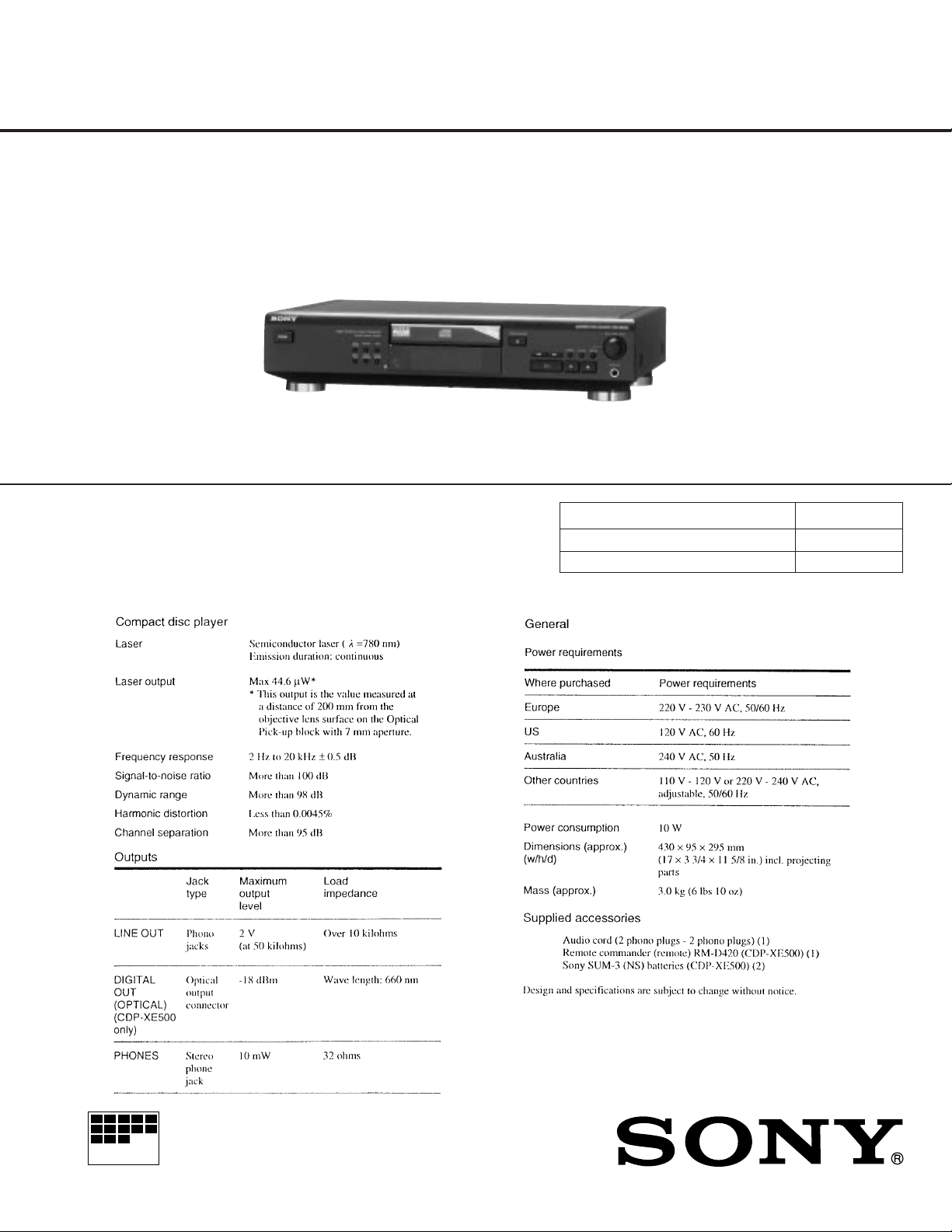
Photo: CDP-XE500
SPECIFICATIONS
US Model
CDP-XE400/XE500
AEP Model
UK Model
E Model
Australian Model
Chinese Model
CDP-XE500
Model Name Using Similar Mechanism CDP-261/361
CD Mechanism Type CDM14-5BD20
Base Unit Name BU-5BD20
MICROFILM
COMPACT DISC PLAYER
– 1 –
Page 2
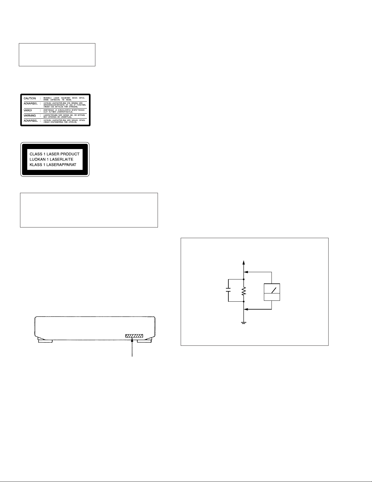
The laser component in this product
is capable of emitting radiation
exceeding the limit for Class 1.
The following caution label is located inside of the unit.
SAFETY CHECK-OUT
After correcting the original service problem, perform the following
safety check before releasing the set to the customer:
Check the antenna terminals, metal trim, “metallized” knobs, screws,
and all other exposed metal parts for AC leakage. Check leakage as
described below.
LEAKAGE TEST
The AC leakage from any exposed metal part to earth ground and
from all exposed metal parts to any exposed metal part having a return to chassis, must not exceed 0.5 mA (500 microampers).
Leakage current can be measured by any one of three methods.
This appliance is classified
as a CLASS 1 LASER
product.
The CLASS 1 LASER
PRODUCT MARKING is
located on the rear exterior.
CAUTION
Use of controls or adjustments or performance of procedures other than those specified herein may result in hazardous radiation exposure.
Notes on Chip Component Replacement
• Never reuse a disconnected chip component.
• Notice that the minus side of a tantalum capacitor may be dam-
aged by heat.
MODEL IDENTIFICATION
– Back Panel –
1. A commercial leakage tester, such as the Simpson 229 or RCA
WT-540A. Follow the manufacturers’ instructions to use these
instruments.
2. A battery-operated A C milliammeter. The Data Precision 245 digital multimeter is suitable for this job.
3. Measuring the voltage drop across a resistor by means of a VOM
or battery-operated AC voltmeter. The “limit” indication is 0.75
V, so analog meters must have an accurate low-voltage scale. The
Simpson 250 and Sanwa SH-63Trd are examples of a passi ve VOM
that is suitable. Nearly all battery operated digital multimeters that
have a 2V AC range are suitable. (See Fig. A)
To Exposed Metal
Parts on Set
0.15µF
1.5k
Ω
AC
voltmeter
(0.75V)
CDP-XE400
US Model : 4-977-587-5π
CDP-XE500
US Model : 4-977-587-1π
E Model : 4-977-587-3π
Australian Model : 4-977-587-4π
Chinese Model : 4-977-587-9π
AEP, German, East European Model : 4-978-388-0π
UK Model : 4-978-388-1π
Earth Ground
Fig. A. Using an AC voltmeter to check AC leakage.
– 2 –
Page 3
NOTES ON HANDLING THE OPTICAL PICK-UP BLOCK OR
BASE UNIT
The laser diode in the optical pick-up block may suffer electrostatic
breakdown because of the potential difference generated by the
charged electrostatic load, etc. on clothing and the human body.
During repair, pay attention to electrostatic breakdown and also use
the procedure in the printed matter which is included in the repair
parts.
The flexible board is easily damaged and should be handled with
care.
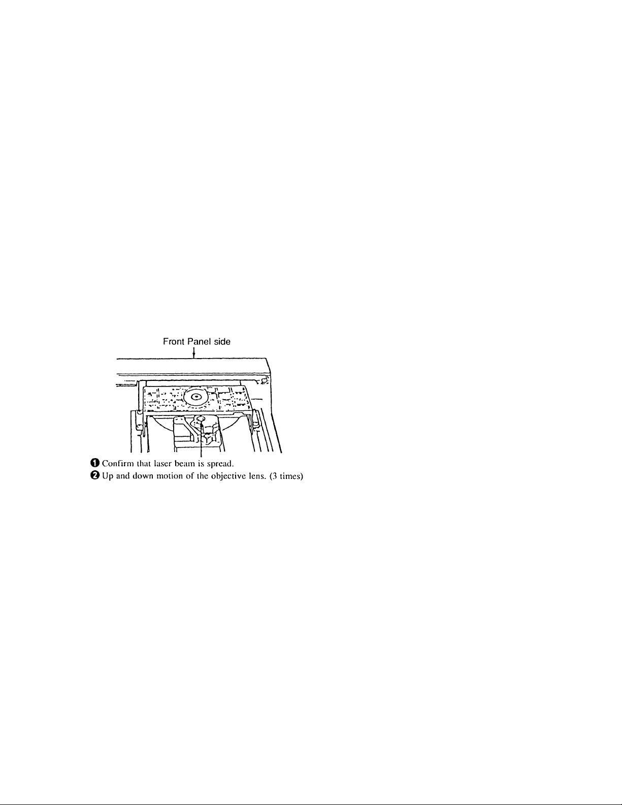
NOTES ON LASER DIODE EMISSION CHECK
The laser beam on this model is concentrated so as to be focused on
the disc reflective surface by the objectiv e lens in the optical pick-up
block. Therefore, when checking the laser diode emission, observe
from more than 30 cm away from the objective lens.
LASER DIODE AND FOCUS SEARCH OPERA TION CHECK
1. Make POWER switch on with no disc inserted and disc table
closed.
2. Confirm that the following operation is performed while
observing the objective lens.
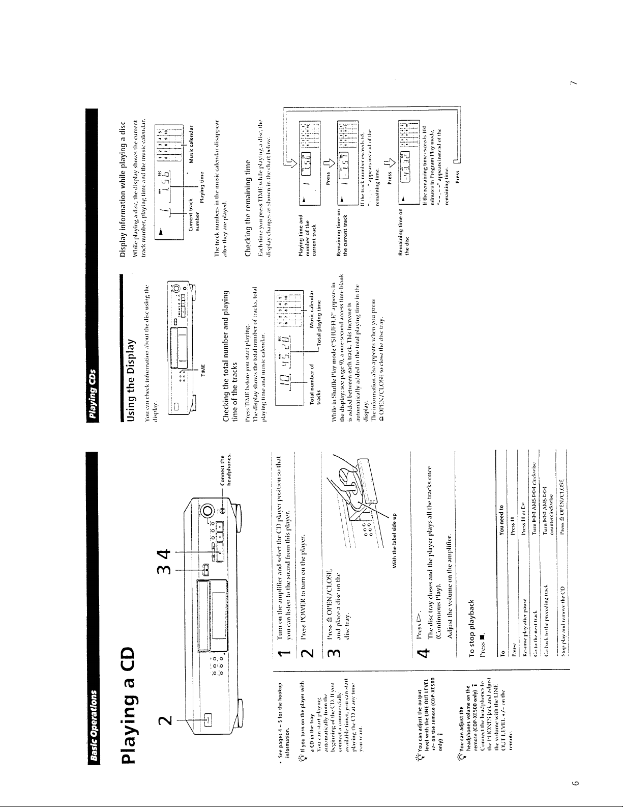
TABLE OF CONTENTS
1. GENERAL
Identifying the Parts .................................................................. 4
Playing a CD.............................................................................. 5
2. DISASSEMBLY
2-1. Front Panel .............................................................................. 6
2-2. Base Unit Block ...................................................................... 6
3. ELECTRICAL BLOCK CHECKING ............................. 7
4. DIAGRAMS
4-1. IC Pin Functions...................................................................... 9
4-2. Printed Wiring Board – BD Section –................................... 13
4-3. Schematic Diagram – BD Section –...................................... 15
4-4. Printed Wiring Boards – Main Section – .............................. 17
4-5. Schematic Diagram – Main Section –................................... 21
5. EXPLODED VIEWS
5-1. Case Section .......................................................................... 28
5-2. Back Panel Section................................................................ 29
5-3. CD Mechanism Section......................................................... 30
5-4. Base Unit Section .................................................................. 31
6. ELECTRICAL PARTS LIST .......................................... 32
SAFETY-RELATED COMPONENT WARNING!!
COMPONENTS IDENTIFIED BY MARK ! OR DOTTED LINE
WITH MARK ! ON THE SCHEMATIC DIAGRAMS AND IN THE
P AR TS LIST ARE CRITICAL TO SAFE OPERATION. REPLACE
THESE COMPONENTS WITH SONY PARTS WHOSE PART
NUMBERS APPEAR AS SHOWN IN THIS MANUAL OR IN
SUPPLEMENTS PUBLISHED BY SONY.
– 3 –
Page 4
Front Panel/Remote
Commander
1 POWER switch
2 PLAY MODE button
3 REPEAT button
4 TIME button
SECTION 1
GENERAL
CONTINUE button
SHUFFLE button
PROGRAM button
5 Disc tray
6 § OPEN/CLOSE button
7 0/) (manual search) button
8 CHECK (program check) button
9 CLEAR (program clear) button
0 ENTER button
!¡ ≠ AMS ± (AMS*) control
!™ PHONES Jack
!£ p (Stop) button
!¢ P (Pause) button
!∞ · (Play) button
!§ Display
!¶ MUSIC SCAN button
!• PEAK SEARCH button
!ª EDIT/TIME button
@º Play Mode buttons
@¡ Numeric buttons
@™ >10 (over 10) button
@£ TIME button
@¢ =/+ (AMS*) button
@∞ FADER button
*AMS is the abbreviation of Automatic
Music Sensor.
•
•
•
•
•
•
•
•
•
•
•
•
•
•••
•
!ª !• !¶ !§ !∞ !¢ !£ !™
@º
98@∞!£!¢
•
•
@¡
@™@£3!∞@¢
••••
•
•
•
7
1234 5 67890!¡
IDENTIFYING THE P ARTS
•
RM-D420 (CDP-XE500 only)
– 4 –
Page 5
– 5 –
Page 6
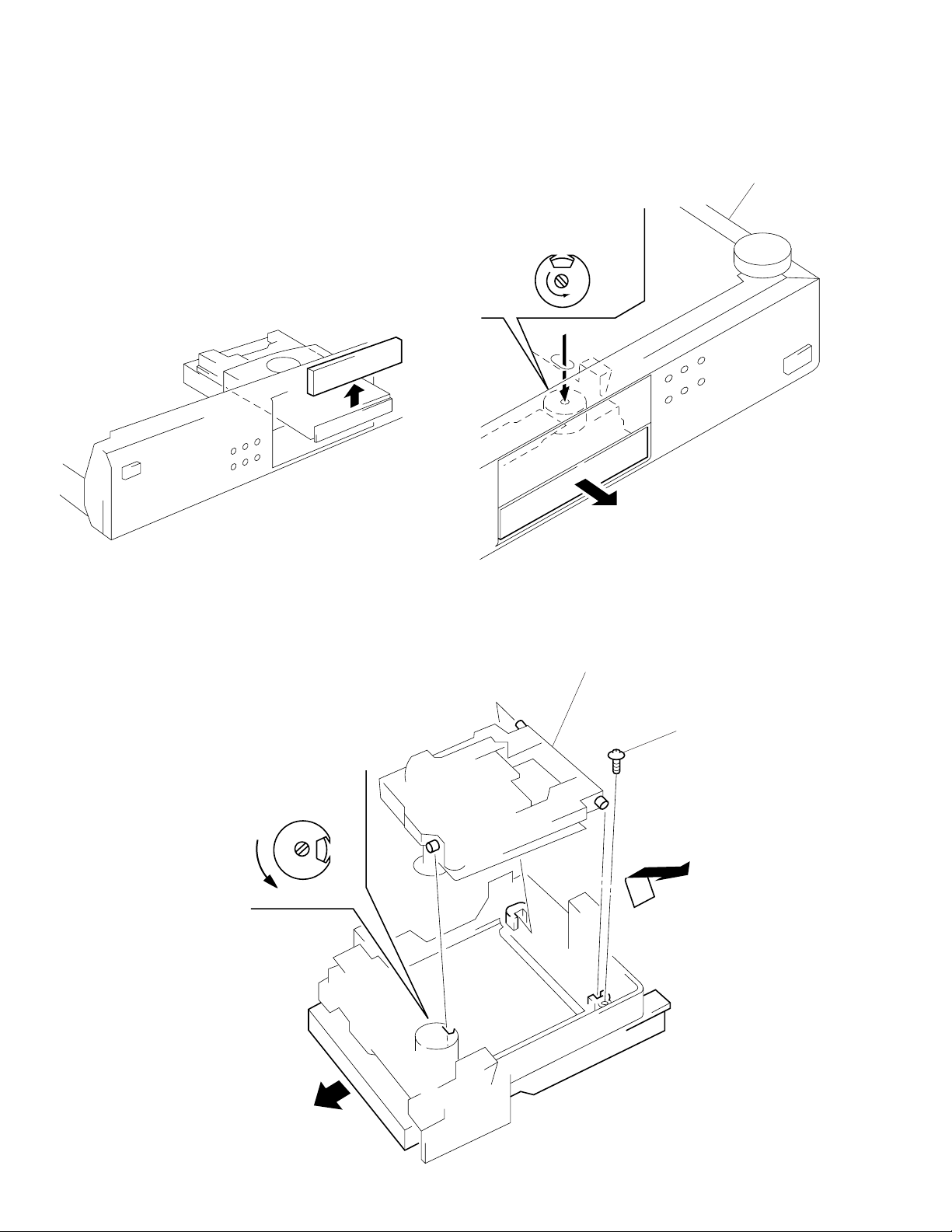
SECTION 2
DISASSEMBLY
Note : Follo w the disassembly procedure in the numerical order giv en.
2-1. FRONT PANEL
• When removing the front panel assembly on electric power failure,
first open the loading block by turning cam with a screwdriver as
shown in the figure, next pull out the loading block with hand, and
remove the loading panel as shown in the figure, then remove the
front panel assembly.
3
Remove loading panel in the arrow direction.
1
Turn in the direction
of the arrow.
bottom of chassis
2-2. BASE UNIT BLOCK
1
Turn the cam to direction of arrow (Counter clockwise) by
minus screw driver.
2
Take off the disc table.
3
Remove the yoke bracket.
4
Remove the MD (BU-5BD20) to the direction of arrow.
1
cam
2
4
BU-5BD20
Pull out disc table.
3
yoke bracket
2
disc table
– 6 –
Page 7
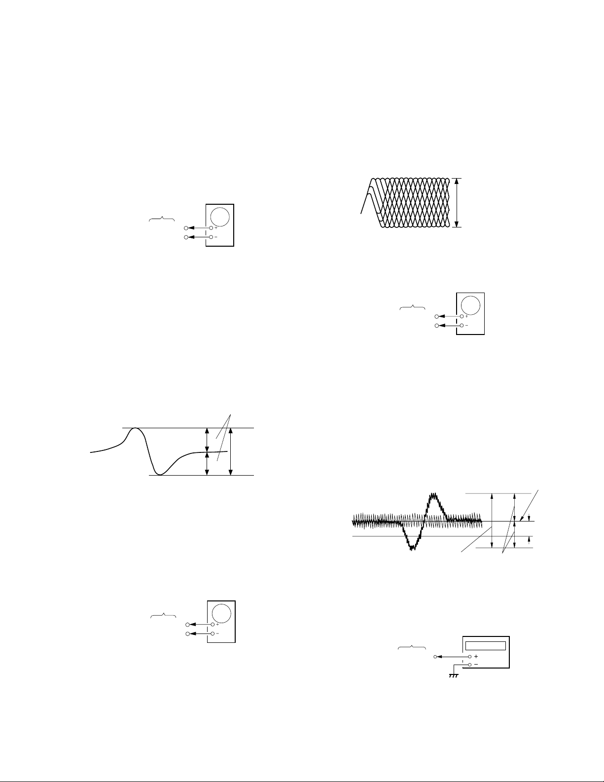
SECTION 3
ELECTRICAL BLOCK CHECKING
Note :
1. CD Block is basically designed to operate without adjustment.
Therefore, check each item in order given.
2. Use YEDS-18 disc (3-702-101-01) unless otherwise indicated.
3. Use an oscilloscope with more than 10MΩ impedance.
4. Clean the objective lens using an applicator with neutral detergent
when the signal level is low than specified value with the follo wing
checks.
S Curve Check
oscilloscope
BD board
TP (FE)
TP (VC)
Procedure :
1. Connect oscilloscope to test point TP (FE) on BD board.
2. Connect between test point TP (FEI) and TP (VC) by lead wire.
3. Turn Power switch on.
4. Put disc (YEDS-18) in and turn Power switch on again and actuate
the focus search. (Actuate the focus search when disc table is moving
in and out.)
5. Check if the oscilloscope waveform (S-curve) is symmetrical
between A and B. And confirm peak to peak le v el within 3±1 Vp-p.
S-curve waveform
symmetry
A
within 3±1 Vp-p
B
3. Put disc (YEDS-18) in and playback.
4. Confirm that oscilloscope waveform is clear and check if RF
signal level is correct or not.
Note :
A clear RF signal waveform means that the shape “ ≈ ” can be
clearly distinguished at the center of the waveform.
RF signal waveform
VOLT/DIV : 200mV
TIME/DIV : 500nS
level : 1.2
+0.25
–0.20
Vp-p
E-F Balance (1 Track Jump) Check
oscilloscope
(DC range)
BD board
TP (TE)
TP (VC)
Procedure :
1. Connect oscilloscope to test point TP (TE) on BD board .
2. Turn Power switch on.
3. Put disc (YEDS-18) in to play the number five track.
4. Press the “P (pause)” button. (Becomes the 1 track jump mode.)
5. Check the level B of the oscilloscope’s waveform and the A (DC
voltage) of the following :
A/B×100 = less than ± 20%.
1 track jump waveform
6. After check, remove the lead wire connected in step 2.
Note : • Try to measure several times to make sure than the ratio of
A : B or B : A is more than 10 : 7.
•Set sweep time as long as possible and set the brightness to
obtain best waveform.
RF Level Check
oscilloscope
BD board
TP (RF)
TP (VC)
Procedure :
1. Connect oscilloscope to test point TP (RF) on BD board.
2. Turn Power switch on.
Center of the waveform
B
level : 1.5±0.7Vp-p
symmetry
RF PLL Free-run Frequency Check
Procedure :
1. Connect frequency counter to test point (PLCK) with lead wire.
frequency counter
MAIN board
TP (PLCK)
2. Turn Power switch on.
3. Confirm that reading on frequency counter is 4.3218MHz.
– 7 –
A (DC voltage)
Page 8

Adjustment Location : BD board
–BD board (conductor side) –
(PLCK)
120
IC103
10 11
IC101
(RF)
(VC)
(FE)
(FEI)
(TE)
– 8 –
Page 9

SECTION 4
DIAGRAMS
4-1. IC PIN FUNCTIONS
• IC101 CXD2545Q (DIGITAL SERVO & DIGITAL SIGNAL PROCESSOR)
Pin No. Pin Name I/O Function
1 SRON O Sled drive output (Not used.)
2 SRDR O Sled drive output
3 SFON O Sled drive output (Not used.)
4 TFDR O Tracking drive output
5 TRON O Tracking drive output (Not used.)
6 TRDR O Tracking drive output
7 TFON O Tracking drive output (Not used.)
8 FFDR O Focus drive output
9 FRON O Focus drive output (Not used.)
10 FRDR O Focus drive output
11 FFON O Focus drive output (Not used.)
12 VCOO O VCO output for analog EFM PLL. (Not used.)
13 VCOI I VCO input for analog EFM PLL. (Ground)
14 TEST I TEST pin connected normally to Ground.
15 DVSS — Digital Ground
16 TES2 I TEST pin connected normally to Ground.
17 TES3 I TEST pin connected normally to Ground.
18 PDO O Charge-pump output for analog EFM PLL. (Not used.)
19 VPCO O Charge-pump output for variable pitch PLL. (Not used.)
20 VCKI I Clock input from variable pitch external VCO. (Ground)
21 AVD2 — Analog power supply
22 IGEN I Power supply pin for operational amplifiers.
23 AVS2 — Analog Ground
24 ADIO I (Not used.)
25 RFC O (Not used.)
26 RFDC I RF signal input
27 TE I Tracking error signal input
28 SE I Sled error signal input
29 FE I Focus error signal input
30 VC I Center voltage input pin
31 FILO O Filter output for master PLL.
32 FILI I Filter input for master PLL.
33 PCO O Charge-pump output for master PLL.
34 CLTV I Control voltage input for master VCO.
35 AVS1 — Analog Ground
36 RFAC I EFM signal input
37 BIAS I Asymmetry circuit constant current input
38 ASYI I Asymmetry comparate voltage input
39 ASYO O EFM full swing output
40 AVD1 — Analog power supply
41 DVDD — Digital power supply
42 ASYE I Asymmetry circuit ON/OFF
43 PSSL I Audio data output mode selection input
44 WDCK O 48-bit slot D/A interface. Word clock
45 LRCK O 48-bit slot D/A interface. LR clock
46 DATA O DA 16 output when PSSL=1. 48-bit slot serial data when PSSL=0.
47 BCLK O DA 15 output when PSSL=1. 48-bit slot data when PSSL=0.
– 9 –
Page 10

Pin No. Pin Name I/O Function
48 64DATA O DA 14 output when PSSL=1. 64-bit slot data when PSSL=0. (Not used.)
49 64BCLK O DA 13 output when PSSL=1. 64-bit slot data when PSSL=0. (Not used.)
50 64LRCK O DA 12 output when PSSL=1. 64-bit slot data when PSSL=0. (Not used.)
51 GTOP O DA 11 output when PSSL=1. GTOP output when PSSL=0. (Not used.)
52 XUGF O DA 10 output when PSSL=1. XUGF output when PSSL=0. (Not used.)
53 XPLCK O DA 09 output when PSSL=1. XPLCK output when PSSL=0.
54 GFS O DA 08 output when PSSL=1. GFS output when PSSL=0.
55 PFCK O DA 07 output when PSSL=1. RFCK output when PSSL=0.
56 C2PO O DA 06 output when PSSL=1. C2PO output when PSSL=0. (Not used.)
57 XRAOF O DA 05 output when PSSL=1. XRAOF output when PSSL=0. (Not used.)
58 MNT3 O DA 04 output when PSSL=1. MNT3 output when PSSL=0.
59 MNT2 O DA 03 output when PSSL=1. MNT2 output when PSSL=0.
60 MNT1 O DA 02 output when PSSL=1. MNT1 output when PSSL=0.
61 MNT0 O DA 01 output when PSSL=1. MNT0 output when PSSL=0.
62 XTAI I X’tal oscillator circuit input
63 XTAO O X’tal oscillator circuit output (Not used.)
64 XTSL I X’tal selection input pin (Ground)
65 DVSS – Digital Ground
66 FSTI I 2/3 divider input of pins 62 and 63.
67 FSTO O 2/3 divider output of pins 62 and 63.
68 FSOF O (Not used.)
69 C16M O 16.9344MHz output (Not used.)
70 MD2 I Digital-out ON/OFF control pin (+5V)
71 DOUT O Digital-out output pin
72 EMPH O Playback disc output in emphasis mode. (Not used.)
73 WFCK O WFCK output
74 SCOR O Sub-code sync output
75 SBSO O Sub-P through Sub-W serial output (Not used.)
76 EXCK I Clock input for SBSO read-out. (Ground)
77 SUBQ O Sub-Q 80-bit output
78 SQCK I Clock input for SQSO read-out.
79 MUTE I Muting selection pin
80 SENS O SENS output
81 XRST I System reset
82 DIRC I Used in 1-track jump mode (+5V)
83 SCLK I SENS serial data read-out clock
84 DFSW I DFCT selection pin (Ground)
85 ATSK I Input pin for anti-shock. (Ground)
86 DATA I Serial data input, supplied from CPU.
87 XLAT I Latch input, supplied from CPU.
88 CLOK I Serial data transfer clock input, supplied from CPU.
89 COUT O Numbers of track counted signal output. (Not used.)
90 DVDD – Digital power supply
91 MIRR O Mirror signal output
92 DFCT O Defect signal output
93 FOK O Focus OK output
94 FSW O Output to select spindle motor output filter. (Not used.)
95 MON O Output to control ON/OFF of spindle motor. (Not used.)
96 MDP O Output to control spindle motor servo
– 10 –
Page 11

Pin No. Pin Name I/O Function
97 MDS O Output to control spindle motor servo. (Not used.)
98 LOCK O GFS is sampled by 460Hz. H when GFS is H. (Not used.)
99 SSTP I Input signal to detect disc innermost track.
100 SFDR O Sled drive output
– 11 –
Page 12

• IC501 CXP82612-021Q (MASTER CONTROL)
Pin No. Pin Name I/O Function
1 TIMER – Connected to +5V.
2 RM I Audio bus input
3 +5V – Connected to +5V.
4-6 – – Not used. (Open)
7 PGML O Latch signal output to digital filter (IC201).
8 CLK O Serial clock output
9 SENSE I SENSE signal input
10 DATA O Serial data output
11 SQCK O Read out clock output for subcode Q data.
12 SUBQ I Subcode Q data input
13 – – Not used. (Open)
14 AMUTE O Analog muting control signal output
15 LDON O Optical pick-up laser diode control output
16 XLT O Serial data latch signal output
17 – – Not used. (Open)
18 RV+ – Not used. (Open)
19 RV- – Not used. (Open)
20 LDOUT O Loading motor control signal output
21 LDIN I Loading motor control signal input
22 KEY0 I Key input (S530)
23 KEY1 I Key input (S520-S527)
24 KEY2 I Key input (S501-S506)
25 KEY3 – Connected to +5V.
26,27 KEY4,KEY5 I Key input (S531)
28 ADJ/AFADJ – ADJ/AFJ test pin
29 IN/OUTSW I Loading IN/OUT switch input
30 RST I Reset signal input
31 EXTAL I Clock input (4MHz)
32 XTAL O Clock output (4MHz)
33 VSS – Ground
34-41 – – Not used. (Open)
42-62 S1-S21 O FL segment output
63-70 1G-7G O FL grid output
71 VFDP(-30V) – -30V pin for FL display tube.
72 VDD(+5V) – +5V pin
73 +5V – +5V pin
74 SEL1 – Connected to Ground.
75-77 – – Connected to Ground.
78 SCOR I Read out timing signal input for subcode Q data.
79,80 SEL2,SEL3 – Connected to +5V.
– 12 –
Page 13

Page 14

Page 15

Page 16

Page 17

NOTE:
• The mechanical parts with no reference
number in the exploded views are not supplied.
• Items marked “*” are not stocked since
they are seldom required for routine service.
Some delay should be anticipated
when ordering these items.
• Abbreviation
AUS : Australian model
CH : Chinese model
G : German model
EE : East European model
5-1. CASE SECTION
CDM14-5BD20
8
SECTION 5
EXPLODED VIEWS
• -XX and -X mean standardized parts, so
they may have some difference from the
original one.
• Color Indication of Appearance Parts
Example :
KNOB, BALANCE (WHITE) ... (RED)
#1
N
Parts Color Cabinet’s Color
2
4
N
• Hardware (# mark) list and accessories
and packing materials are given in the
last of this parts list.
The components identified by
mark ! or dotted line with mark.
! are critical for safety.
Replace only with part number
specified.
1
#1
3
9
7
5
2
5
11
10
24
12
not supplied
5
6
5
13
16
5
20
19
17
Ref. No. Part No. Description Remark Ref. No. Part No. Description Remark
* 1 4-978-901-21 CASE (408226) (BLACK)
* 1 4-978-901-91 CASE (408226) (SILVER)
2 3-363-099-01 SCREW (CASE 3 TP2) (AEP,UK,G,EE)
2 3-704-366-31 SCREW (CASE) (M3X6) (US,E,AUS,CH)
3 4-956-370-02 BAND, PLUG FIXED (UK,AUS)
18
#1
supplied with J601
11 X-4946-531-1 PANEL ASSY, FRONT (AEP:BLACK,UK,G,EE)
11 X-4946-957-1 PANEL ASSY, FRONT (SILVER)
12 X-4947-021-1 PANEL ASSY, FRONT (XE500:E, AUS, CH)
12 X-4947-022-1 PANEL ASSY, FRONT (XE500:US)
12 X-4947-083-1 PANEL ASSY, FRONT (XE400)
not supplied
4 1-776-100-11 WIRE (FLAT TYPE) (23 CORE)
5 4-951-620-01 SCREW (2.6X8), +BVTP
6 1-776-099-11 WIRE (FLAT TYPE) (21 CORE)
* 7 A-4673-727-A PANEL BOARD, COMPLETE
* 8 1-658-840-11 POWER SW BOARD
9 4-977-589-01 BUTTON (POWER) (BLACK)
9 4-977-589-11 BUTTON (POWER) (SILVER)
10 4-977-588-01 PANEL, LOADING (XE500:BLACK)
10 4-977-588-11 PANEL, LOADING (XE400)
10 4-977-588-41 PANEL, LOADING (XE500:SILVER)
13 4-963-404-21 EMBLEM (5-A), SONY (US,E,AUS,CH)
16 4-977-583-01 BUTTON (PLAY) (BLACK)
17 4-977-590-01 KNOB (AMS) (US,E,AUS,CH)
17 4-977-590-11 KNOB (AMS) (SILVER)
18 3-354-981-01 SPRING (SUS), RING
* 19 1-658-839-11 H.P BOARD
20 X-4947-207-1 FOOT ASSY (F50150S) (BLACK)
20 X-4947-124-1 FOOT ASSY (F50150S) (SILVER)
24 4-977-584-11 BUTTON (MODE)
– 28 –
Page 18

5-2. BACK PANEL SECTION
UK Model US Model AEP, G, EE Model E Model
CNP901
CNP901
CNP901
CNP901
55
52
54
53
#1
#1
T901
51
#2
not supplied
#1
#1
CH Model
CNP901
56
AUS Model
CNP901
The components identified by
mark ! or dotted line with mark.
! are critical for safety.
Replace only with part number
specified.
Ref. No. Part No. Description Remark Ref. No. Part No. Description Remark
51 3-703-244-00 BUSHING, CORD (EXCEPT US,E)
* 51 3-703-571-11 BUSHING (S) (4516), CORD (US,E)
* 52 4-977-587-11 PANEL, BACK (XE500:US)
* 52 4-977-587-31 PANEL, BACK (E)
* 52 4-977-587-41 PANEL, BACK (AUS)
* 52 4-977-587-51 PANEL, BACK (XE400)
* 52 4-977-587-91 PANEL, BACK (CH)
* 52 4-978-388-01 PANEL, BACK (AEP,G,EE)
* 52 4-978-388-11 PANEL, BACK (UK)
* 53 A-4673-738-A MAIN BOARD, COMPLETE (XE400)
* 53 A-4673-739-A MAIN BOARD, COMPLETE (E)
53 A-4673-740-A MAIN BOARD, COMPLETE (EXCEPT US,E)
53 A-4673-753-A MAIN BOARD, COMPLETE (XE500:US)
* 54 4-954-051-51 HOLDER, PC BOARD
! 55 1-569-007-11 ADAPTOR, CONVERSION 2P (E)
! 56 1-569-008-11 ADAPTOR, CONVERSION 2P (CH)
! CNP901 1-558-943-81 CORD, POWER (E)
! CNP901 1-558-945-21 CORD, POWER (POLAR.SPT-1) (US)
! CNP901 1-575-651-21 CORD, POWER (AEP,G,EE)
! CNP901 1-696-845-11 CORD, POWER (AUS)
! CNP901 1-696-907-11 CORD, POWER (UK)
! CNP901 1-696-966-11 CORD, POWER (CH)
! T901 1-423-979-11 TRANSFORMER, POWER (EXCEPT US,E)
! T901 1-426-621-11 TRANSFORMER, POWER (US)
! T901 1-426-622-11 TRANSFORMER, POWER (E)
– 29 –
Page 19

5-3. CD MECHANISM SECTION
(CDM14-5BD20)
108
109
110
107
106
104
111
115
113
112
BU-5BD20
114
105
#3
103
102
M151
101
Ref. No. Part No. Description Remark Ref. No. Part No. Description Remark
* 101 1-645-721-11 LOADING BOARD
102 4-933-111-11 CHASSIS (MD) (AEP,UK,G,EE)
102 4-933-111-41 CHASSIS (MD) (US,E,AUS,CH)
* 103 4-917-583-21 BRACKET, YOKE
104 4-927-649-01 BELT
105 4-933-109-01 CAM
106 4-927-651-01 PULLEY (S)
107 4-967-268-01 GEAR (C)
108 4-933-107-01 GEAR (PL)
109 4-933-112-11 TABLE, DISC
110 4-933-110-41 HOLDER (MG)
* 111 1-452-538-11 MAGNET
112 4-933-134-01 SCREW (+PTPWH M2.6X6)
113 4-959-996-01 SPRING (932), COMPRESSION
114 4-933-129-01 HOLDER (BU)
115 4-925-315-31 DAMPER
M151 A-4604-363-A MOTOR (L) ASSY (LOADING)
– 30 –
Page 20

5-4. BASE UNIT SECTION
(BU-5BD20)
155
r
A
156
#4
153
152
151
M101
(Including rA)
M102
152
158
157
#5
The components identified by
mark ! or dotted line with mark.
! are critical for safety.
Replace only with part number
specified.
Ref. No. Part No. Description Remark Ref. No. Part No. Description Remark
151 A-4673-509-A BD BOARD, COMPLETE (US,E,AUS,CH)
* 151 A-4673-511-A BD BOARD, COMPLETE (AEP,UK,G,EE)
152 4-951-940-01 INSULATOR (BU)
153 4-917-565-01 SHAFT, SLED
! 155 8-848-367-11 PICK-UP BLOCK, OPTICAL KSS-213B/K-N
156 4-917-567-21 GEAR (M)
157 4-917-564-01 GEAR (P), FLATNESS
158 1-769-069-11 WIRE (FLAT TYPE) (16 CORE)
M101 X-4917-523-3 BASE (OUTSERT) ASSY (SPINDLE)
M102 X-4917-504-1 MOTOR ASSY (SLED)
– 31 –
Page 21

SECTION 6
BD
NOTE:
• Due to standardization, replacements in
the parts list may be different from the
parts specified in the diagrams or the
components used on the set.
• -XX and -X mean standardized parts, so
they may have some difference from the
original one.
• RESISTORS
All resistors are in ohms.
METAL:Metal-film resistor.
METAL OXIDE: Metal oxide-film resistor.
F:nonflammable
Ref. No. Part No. Description Remark Ref. No. Part No. Description Remark
A-4673-509-A BD BOARD, COMPLETE (US,E,AUS,CH)
* A-4673-511-A BD BOARD, COMPLETE (AEP,UK,G,EE)
*******************
< CAPACITOR >
C101 1-163-005-11 CERAMIC CHIP 470PF 10% 50V
C102 1-163-038-00 CERAMIC CHIP 0.1uF 25V
C103 1-163-005-11 CERAMIC CHIP 470PF 10% 50V
C105 1-135-155-21 TANT ALUM CHIP 4.7uF 10% 16V
C106 1-164-346-11 CERAMIC CHIP 1uF 16V
C107 1-164-346-11 CERAMIC CHIP 1uF 16V
C108 1-163-035-00 CERAMIC CHIP 0.047uF 50V
C109 1-163-145-00 CERAMIC CHIP 0.0015uF 5% 50V
C110 1-163-017-00 CERAMIC CHIP 0.0047uF 5% 50V
C111 1-163-251-11 CERAMIC CHIP 100PF 5% 50V
C112 1-163-038-00 CERAMIC CHIP 0.1uF 25V
C113 1-163-038-00 CERAMIC CHIP 0.1uF 25V
C115 1-126-607-11 ELECT CHIP 47uF 20% 4V
C116 1-126-607-11 ELECT CHIP 47uF 20% 4V
C117 1-126-209-11 ELECT 100uF 20% 4V
C118 1-163-275-11 CERAMIC CHIP 0.001uF 5% 50V
C119 1-163-231-11 CERAMIC CHIP 15PF 5% 50V
C123 1-164-232-11 CERAMIC CHIP 0.01uF 50V
C124 1-164-005-11 CERAMIC CHIP 0.47uF 25V
C140 1-163-038-00 CERAMIC CHIP 0.1uF 25V
C141 1-163-038-00 CERAMIC CHIP 0.1uF 25V
C151 1-163-237-11 CERAMIC CHIP 27PF 5% 50V
C153 1-163-038-00 CERAMIC CHIP 0.1uF 25V
C154 1-164-336-11 CERAMIC CHIP 0.33uF 25V
C156 1-163-237-11 CERAMIC CHIP 27PF 5% 50V
C157 1-163-145-00 CERAMIC CHIP 0.0015uF 5% 50V
C159 1-163-019-00 CERAMIC CHIP 0.0068uF 10% 50V
C161 1-163-038-00 CERAMIC CHIP 0.1uF 25V
< CONNECTOR >
CN101 1-770-072-11 CONNECTOR, FFC 23P
CN102 1-770-014-11 CONNECTOR, FFC/FPC 16P
< IC >
IC101 8-752-369-78 IC CXD2545Q
IC102 8-759-176-09 IC BA6392FP
IC103 8-752-072-45 IC CXA1821M-T6
ELECTRICAL PARTS LIST
• Items marked “*” are not stocked since
they are seldom required for routine service.
Some delay should be anticipated
when ordering these items.
• SEMICONDUCTORS
In each case, u : µ, for example:
uA.. : µA.. uPA.. : µPA..
uPB.. : µPB.. uPC.. : µPC.. uPD.. : µPD..
• CAPACITORS
uF : µF
• COILS
uH : µH
Q101 8-729-010-08 TRANSISTOR MSB710-R
R101 1-216-077-00 METAL CHIP 15K 5% 1/10W
R102 1-216-097-00 METAL GLAZE 100K 5% 1/10W
R103 1-216-077-00 METAL CHIP 15K 5% 1/10W
R104 1-216-085-00 METAL CHIP 33K 5% 1/10W
R105 1-216-097-00 METAL GLAZE 100K 5% 1/10W
R106 1-216-061-00 METAL CHIP 3.3K 5% 1/10W
R107 1-216-061-00 METAL CHIP 3.3K 5% 1/10W
R108 1-216-073-00 METAL CHIP 10K 5% 1/10W
R109 1-216-121-00 METAL GLAZE 1M 5% 1/10W
R110 1-216-025-00 METAL GLAZE 100 5% 1/10W
R112 1-216-049-11 METAL GLAZE 1K 5% 1/10W
R123 1-216-073-00 METAL CHIP 10K 5% 1/10W
R124 1-216-097-00 METAL GLAZE 100K 5% 1/10W
R125-127
1-216-049-11 METAL GLAZE 1K 5% 1/10W
R131 1-216-037-00 METAL CHIP 330 5% 1/10W
R135-138
1-216-295-00 CONDUCTOR, CHIP (2012)
R141 1-216-089-00 METAL GLAZE 47K 5% 1/10W
R142 1-216-081-00 METAL CHIP 22K 5% 1/10W
R143 1-216-103-00 METAL GLAZE 180K 5% 1/10W
R144 1-216-103-00 METAL GLAZE 180K 5% 1/10W
R146 1-216-073-00 METAL CHIP 10K 5% 1/10W
R147 1-216-081-00 METAL CHIP 22K 5% 1/10W
R148 1-216-001-00 METAL CHIP 10 5% 1/10W
R149 1-216-003-11 METAL GLAZE 12 5% 1/10W
R158 1-216-111-00 METAL GLAZE 390K 5% 1/10W
R159 1-216-101-00 METAL CHIP 150K 5% 1/10W
R160 1-216-295-00 CONDUCTOR, CHIP (2012)
R161 1-216-308-00 METAL CHIP 4.7 5% 1/10W
R162 1-216-101-00 METAL CHIP 150K 5% 1/10W
S101 1-572-085-11 SWITCH, LEAF (LIMIT SW)
**************************************************************
The components identified by mark
! or dotted line with mark. ! are
critical for safety.
Replace only with part number
specified.
When indicating parts by reference
number, please include the board.
• Abbreviation
AUS : Australian model
CH : Chinese model
G : German model
EE : East European model
< TRANSISTOR >
< RESISTOR >
< SWITCH >
– 32 –
Page 22

H.P
Ref. No. Part No. Description Remark Ref. No. Part No. Description Remark
* 1-658-839-11 H.P BOARD
*********
< CAPACITOR >
C604 1-162-291-31 CERAMIC 560PF 10% 50V
C605 1-162-291-31 CERAMIC 560PF 10% 50V
C608 1-164-159-21 CERAMIC 0.1uF 50V
< CONNECTOR >
* CN601 1-568-941-11 PIN, CONNECTOR 3P
< JACK >
J601 1-568-519-41 JACK, LARGE TYPE (PHONES)
< COIL >
L601-603
1-410-397-21 FERRITE BEAD INDUCTOR 1.1uH
**************************************************************
* 1-645-721-11 LOADING BOARD
**************
< CONNECTOR >
* CN151 1-568-943-11 PIN, CONNECTOR 5P
< SWITCH >
S151 1-572-086-11 SWITCH, LEAF (LOAD OUT)
S152 1-572-086-11 SWITCH, LEAF (LOAD IN)
**************************************************************
* A-4673-738-A MAIN BOARD, COMPLETE (XE400)
* A-4673-739-A MAIN BOARD, COMPLETE (E)
* A-4673-740-A MAIN BOARD, COMPLETE (EXCEPT US,E)
* A-4673-753-A MAIN BOARD, COMPLETE (XE500:US)
*********************
< CAPACITOR >
C201 1-101-006-00 CERAMIC 0.047uF 50V
(US,E,AUS,CH)
C201 1-161-494-00 CERAMIC 0.022uF 25V
(AEP,UK,G,EE)
C202 1-162-290-31 CERAMIC 470PF 10% 50V
C205 1-104-666-11 ELECT 220uF 20% 25V
C211 1-101-006-00 CERAMIC 0.047uF 50V
(US,E,AUS,CH)
C211 1-161-494-00 CERAMIC 0.022uF 25V
(AEP,UK,G,EE)
C251 1-162-282-31 CERAMIC 100PF 10% 50V
C252 1-101-006-00 CERAMIC 0.047uF 50V
(US,E,AUS,CH)
C252 1-161-494-00 CERAMIC 0.022uF 25V
(AEP,UK,G,EE)
C253 1-126-933-11 ELECT 100uF 20% 16V
C254 1-162-199-31 CERAMIC 10PF 5% 50V
C255 1-162-199-31 CERAMIC 10PF 5% 50V
C256 1-101-006-00 CERAMIC 0.047uF 50V
C256 1-161-494-00 CERAMIC 0.022uF 25V
C257 1-126-933-11 ELECT 100uF 20% 16V
C258 1-101-006-00 CERAMIC 0.047uF 50V
C258 1-161-494-00 CERAMIC 0.022uF 25V
C259 1-126-933-11 ELECT 100uF 20% 16V
C264 1-162-282-31 CERAMIC 100PF 10% 50V
C280 1-164-159-21 CERAMIC 0.1uF 50V
C301 1-162-215-31 CERAMIC 47PF 5% 50V
C302 1-130-479-00 MYLAR 0.0047uF 5% 50V
C303 1-126-933-11 ELECT 100uF 20% 16V
C304 1-162-215-31 CERAMIC 47PF 5% 50V
C305 1-130-472-00 MYLAR 0.0012uF 5% 50V
C306 1-101-006-00 CERAMIC 0.047uF 50V
C306 1-161-494-00 CERAMIC 0.022uF 25V
C307 1-162-291-31 CERAMIC 560PF 10% 50V
C351 1-162-215-31 CERAMIC 47PF 5% 50V
C352 1-130-479-00 MYLAR 0.0047uF 5% 50V
C353 1-126-933-11 ELECT 100uF 20% 16V
C354 1-162-215-31 CERAMIC 47PF 5% 50V
C355 1-130-472-00 MYLAR 0.0012uF 5% 50V
C356 1-101-006-00 CERAMIC 0.047uF 50V
C356 1-161-494-00 CERAMIC 0.022uF 25V
C357 1-162-291-31 CERAMIC 560PF 10% 50V
C400 1-126-964-11 ELECT 10uF 20% 50V
C401 1-101-006-00 CERAMIC 0.047uF 50V
C401 1-161-494-00 CERAMIC 0.022uF 25V
C402 1-162-306-11 CERAMIC 0.01uF 30% 16V
C403 1-104-666-11 ELECT 220uF 20% 25V
C404 1-101-006-00 CERAMIC 0.047uF 50V
C404 1-161-494-00 CERAMIC 0.022uF 25V
C481 1-101-006-00 CERAMIC 0.047uF 50V
C481 1-161-494-00 CERAMIC 0.022uF 25V
C601 1-101-006-00 CERAMIC 0.047uF 50V
C601 1-161-494-00 CERAMIC 0.022uF 25V
LOADING
(XE500:US,E,AUS,CH)
MAIN
(US,E,AUS,CH)
(AEP,UK,G,EE)
(US,E,AUS,CH)
(AEP,UK,G,EE)
(US,E,AUS,CH)
(AEP,UK,G,EE)
(US,E,AUS,CH)
(AEP,UK,G,EE)
(US,E,AUS,CH)
(AEP,UK,G,EE)
(XE500)
(AEP,UK,G,EE)
(US,E,AUS,CH)
(AEP,UK,G,EE)
(US,E,AUS,CH)
(AEP,UK,G,EE)
– 33 –
Page 23

MAIN
Ref. No. Part No. Description Remark Ref. No. Part No. Description Remark
C602 1-101-006-00 CERAMIC 0.047uF 50V
(US,E,AUS,CH)
C602 1-161-494-00 CERAMIC 0.022uF 25V
(AEP,UK,G,EE)
C607 1-101-006-00 CERAMIC 0.047uF 50V
(US,E,AUS,CH)
C607 1-161-494-00 CERAMIC 0.022uF 25V
(AEP,UK,G,EE)
C680 1-101-006-00 CERAMIC 0.047uF 50V
(US,E,AUS,CH)
C680 1-161-494-00 CERAMIC 0.022uF 25V
(AEP,UK,G,EE)
C702 1-126-964-11 ELECT 10uF 20% 50V
C703 1-162-294-31 CERAMIC 0.001uF 10% 50V
C704 1-104-666-11 ELECT 220uF 20% 25V
C705 1-126-964-11 ELECT 10uF 20% 50V
C706 1-126-933-11 ELECT 100uF 20% 16V
C707 1-124-903-11 ELECT 1uF 20% 50V
C708-710
1-126-964-11 ELECT 10uF 20% 50V
C711 1-124-903-11 ELECT 1uF 20% 50V
C712 1-124-903-11 ELECT 1uF 20% 50V
D403 8-719-010-34 DIODE UZ-4.7BSC
D701 8-719-815-85 DIODE 1S1585
D702 8-719-815-85 DIODE 1S1585
D703 8-719-815-85 DIODE 1S1585
D704 8-719-815-85 DIODE 1S1585
D705 8-719-815-85 DIODE 1S1585
D706 8-719-815-85 DIODE 1S1585 (AEP,UK,G,EE)
D707 8-719-815-85 DIODE 1S1585
D708 8-719-815-85 DIODE 1S1585 (AEP,UK,G,EE)
D901 8-719-200-82 DIODE 11ES2
D902 8-719-200-82 DIODE 11ES2
D903 8-719-200-82 DIODE 11ES2
D904 8-719-200-82 DIODE 11ES2
D905 8-719-200-82 DIODE 11ES2
< IC >
IC201 8-759-362-47 IC CXD8567AM
IC301 8-759-634-51 IC M5218AP
IC302 8-759-634-51 IC M5218AP
IC401 8-759-822-09 IC LB1641
IC601 8-759-634-51 IC M5218AP
C901 1-126-939-11 ELECT 10000uF 20% 16V
C902 1-126-768-11 ELECT 2200uF 20% 16V
C903 1-128-576-11 ELECT 100uF 20% 63V
C904 1-101-006-00 CERAMIC 0.047uF 50V
(US,E,AUS,CH)
C904 1-161-494-00 CERAMIC 0.022uF 25V
(AEP,UK,G,EE)
C905 1-101-006-00 CERAMIC 0.047uF 50V
(US,E,AUS,CH)
C905 1-161-494-00 CERAMIC 0.022uF 25V
(AEP,UK,G,EE)
C906 1-101-006-00 CERAMIC 0.047uF 50V
(US,E,AUS,CH)
C906 1-164-159-21 CERAMIC 0.1uF 50V
(AEP,UK,G,EE)
C907 1-101-006-00 CERAMIC 0.047uF 50V
(US,E,AUS,CH)
C907 1-164-159-21 CERAMIC 0.1uF 50V
(AEP,UK,G,EE)
C908 1-101-006-00 CERAMIC 0.047uF 50V
(US,E,AUS,CH)
C908 1-164-159-21 CERAMIC 0.1uF 50V
(AEP,UK,G,EE)
< CONNECTOR >
* CN201 1-568-839-11 SOCKET, CONNECTOR 23P
CN202 1-568-838-11 SOCKET, CONNECTOR 21P
CN901 1-580-230-11 PIN, CONNECTOR (PC BOARD) 2P (AEP,UK,G,EE)
< DIODE >
D400 8-719-982-22 DIODE MTZJ-30D
D401 8-719-815-85 DIODE 1S1585
D402 8-719-109-97 DIODE RD6.8ES-B2
IC701 8-759-821-93 IC LA5601
IC801 8-749-921-12 IC GP1F32T (DIGITAL OUT OPTICAL) (XE500)
< JACK >
J301 1-770-719-11 JACK, PIN 2P (LINE OUT VARIABLE)
< COIL >
L201 1-410-322-11 INDUCTOR 3.3uH (EXCEPT US)
L205 1-410-322-11 INDUCTOR 3.3uH (XE500)
L206 1-410-507-11 INDUCTOR 6.8uH (XE500)
L211 1-410-507-11 INDUCTOR 6.8uH (XE500)
L220 1-410-322-11 INDUCTOR 3.3uH
L251 1-410-322-11 INDUCTOR 3.3uH
L253 1-410-322-11 INDUCTOR 3.3uH
L254 1-410-397-21 FERRITE BEAD INDUCTOR 1.1uH (US)
L254 1-410-507-11 INDUCTOR 6.8uH (EXCEPT US)
L701 1-414-223-11 INDUCTOR 470uH
L702 1-412-473-21 INDUCTOR 0uH (US)
< TRANSISTOR >
Q301 8-729-922-37 TRANSISTOR 2SD2144S
Q351 8-729-922-37 TRANSISTOR 2SD2144S
Q400 8-729-230-46 TRANSISTOR 2SA1048TP-YG
Q401 8-729-019-64 TRANSISTOR 2SB1041
Q601 8-729-922-37 TRANSISTOR 2SD2144S
Q602 8-729-922-37 TRANSISTOR 2SD2144S
Q701 8-729-029-56 TRANSISTOR DTA144ESA-TP
Q702 8-729-029-56 TRANSISTOR DTA144ESA-TP
– 34 –
Page 24

PANELMAIN
Ref. No. Part No. Description Remark Ref. No. Part No. Description Remark
< RESISTOR >
R201 1-249-417-11 CARBON 1K 5% 1/4W
R202 1-247-807-11 CARBON 100 5% 1/4W (US)
R202 1-247-815-00 CARBON 220 5% 1/4W
(EXCEPT US)
R203-208
1-249-417-11 CARBON 1K 5% 1/4W
R220 1-247-815-00 CARBON 220 5% 1/4W (US)
R702 1-249-441-11 CARBON 100K 5% 1/4W
R703 1-249-441-11 CARBON 100K 5% 1/4W
R704 1-247-807-11 CARBON 100 5% 1/4W
R705 1-249-417-11 CARBON 1K 5% 1/4W
< SWITCH >
! S901 1-572-675-11 SWITCH, POWER VOLTAGE CHANGE
(VOLTAGE SELECTOR) (E)
R221 1-247-804-11 CARBON 75 5% 1/4W (US)
R221 1-249-400-11 CARBON 39 5% 1/4W
(EXCEPT US)
R251 1-249-436-11 CARBON 39K 5% 1/4W
R252 1-249-436-11 CARBON 39K 5% 1/4W
R253
1-249-424-11 CARBON 3.9K 5% 1/4W
R255 1-249-436-11 CARBON 39K 5% 1/4W
R256 1-249-436-11 CARBON 39K 5% 1/4W
R257 1-247-807-11 CARBON 100 5% 1/4W
R301 1-249-431-11 CARBON 15K 5% 1/4W
R302 1-249-431-11 CARBON 15K 5% 1/4W
R303 1-249-437-11 CARBON 47K 5% 1/4W
R304 1-249-419-11 CARBON 1.5K 5% 1/4W
R305 1-249-419-11 CARBON 1.5K 5% 1/4W
R306 1-249-417-11 CARBON 1K 5% 1/4W
R307 1-249-437-11 CARBON 47K 5% 1/4W
R308 1-249-441-11 CARBON 100K 5% 1/4W
R309 1-249-419-11 CARBON 1.5K 5% 1/4W
R310 1-247-807-11 CARBON 100 5% 1/4W
R351 1-249-431-11 CARBON 15K 5% 1/4W
R352 1-249-431-11 CARBON 15K 5% 1/4W
R353 1-249-437-11 CARBON 47K 5% 1/4W
R354 1-249-419-11 CARBON 1.5K 5% 1/4W
R355 1-249-419-11 CARBON 1.5K 5% 1/4W
R356 1-249-417-11 CARBON 1K 5% 1/4W
R357 1-249-437-11 CARBON 47K 5% 1/4W
R358 1-249-441-11 CARBON 100K 5% 1/4W
R359 1-249-419-11 CARBON 1.5K 5% 1/4W
R360 1-247-807-11 CARBON 100 5% 1/4W
R400 1-249-432-11 CARBON 18K 5% 1/4W
R401 1-249-432-11 CARBON 18K 5% 1/4W
< TRANSFORMER >
! T901 1-423-979-11 TRANSFORMER, POWER (EXCEPT US,E)
! T901 1-426-621-11 TRANSFORMER, POWER (US)
! T901 1-426-622-11 TRANSFORMER, POWER (E)
< TERMINAL >
* TPT901 1-535-771-11 TERMINAL (US,E,AUS,CH)
* TPT902 1-535-771-11 TERMINAL (US,E,AUS,CH)
< VIBRATOR >
X201 1-579-833-21 VIBRATOR, CRYSTAL (33.8688MHz) (XE400)
X201 1-579-834-11 VIBRATOR, CRYSTAL (33.8688MHz) (XE500)
**************************************************************
* A-4673-727-A PANEL BOARD, COMPLETE
**********************
< CAPACITOR >
C501-503
1-161-494-00 CERAMIC 0.022uF 25V
C505 1-161-494-00 CERAMIC 0.022uF 25V
< CONNECTOR >
* CN501 1-568-864-11 SOCKET, CONNECTOR 21P
< FLUORESCENT INDICATOR TUBE >
FL501 1-517-297-21 INDICATOR TUBE, FLUORESCENT
< IC >
IC501 8-752-869-51 IC CXP82612-021Q
IC502 8-741-810-59 IC SBX1810-59
R402 1-249-441-11 CARBON 100K 5% 1/4W
R403 1-249-425-11 CARBON 4.7K 5% 1/4W
R404 1-249-441-11 CARBON 100K 5% 1/4W
R405 1-249-432-11 CARBON 18K 5% 1/4W
R406 1-249-427-11 CARBON 6.8K 5% 1/4W
R451 1-249-427-11 CARBON 6.8K 5% 1/4W
R601 1-249-403-11 CARBON 68 5% 1/4W
R602 1-249-403-11 CARBON 68 5% 1/4W
R603 1-249-419-11 CARBON 1.5K 5% 1/4W
R604 1-249-419-11 CARBON 1.5K 5% 1/4W
R701 1-249-422-11 CARBON 2.7K 5% 1/4W
< TRANSISTOR >
Q501 8-729-029-67 TRANSISTOR DTC114ESA-TP
< RESISTOR >
R501 1-249-427-11 CARBON 6.8K 5% 1/4W
R502 1-249-427-11 CARBON 6.8K 5% 1/4W
R503 1-249-431-11 CARBON 15K 5% 1/4W
R504 1-249-427-11 CARBON 6.8K 5% 1/4W
R505 1-249-415-11 CARBON 680 5% 1/4W
R506 1-249-417-11 CARBON 1K 5% 1/4W
The components identified by mark
! or dotted line with mark. ! are
critical for safety.
Replace only with part number
specified.
– 35 –
Page 25

PANEL POWER SW
Ref. No. Part No. Description Remark Ref. No. Part No. Description Remark
R507 1-249-419-11 CARBON 1.5K 5% 1/4W
R508 1-249-421-11 CARBON 2.2K 5% 1/4W
R509 1-249-423-11 CARBON 3.3K 5% 1/4W
R510 1-249-427-11 CARBON 6.8K 5% 1/4W
R511 1-249-415-11 CARBON 680 5% 1/4W
R512 1-249-417-11 CARBON 1K 5% 1/4W
R513 1-249-419-11 CARBON 1.5K 5% 1/4W
R514 1-249-421-11 CARBON 2.2K 5% 1/4W
R515 1-249-423-11 CARBON 3.3K 5% 1/4W
R516 1-249-427-11 CARBON 6.8K 5% 1/4W
R517 1-249-431-11 CARBON 15K 5% 1/4W
R519 1-249-441-11 CARBON 100K 5% 1/4W
R520 1-249-427-11 CARBON 6.8K 5% 1/4W
R530 1-249-429-11 CARBON 10K 5% 1/4W
R531 1-249-429-11 CARBON 10K 5% 1/4W
< SWITCH >
S501 1-554-303-21 SWITCH, TACTILE (MUSIC SCAN)
S502 1-554-303-21 SWITCH, TACTILE (PEAK SEARCH)
S503 1-554-303-21 SWITCH, TACTILE (EDIT/TIME)
S504 1-554-303-21 SWITCH, TACTILE (PLAY MODE)
S505 1-554-303-21 SWITCH, TACTILE (REPEAT)
S506 1-554-303-21 SWITCH, TACTILE (TIME)
S520 1-554-303-21 SWITCH, TACTILE (·)
S521 1-554-303-21 SWITCH, TACTILE (P)
S522 1-554-303-21 SWITCH, TACTILE (p)
S523 1-554-303-21 SWITCH, TACTILE (ENTER)
S524 1-554-303-21 SWITCH, TACTILE (CLEAR)
S525 1-554-303-21 SWITCH, TACTILE (CHECK)
S526 1-554-303-21 SWITCH, TACTILE ())
S527 1-554-303-21 SWITCH, TACTILE (0)
S530 1-554-303-21 SWITCH, TACTILE (§ OPEN/CLOSE)
S531 1-473-452-11 ENCODER, ROTARY (≠ AMS ±)
< VIBRATOR >
X501 1-577-082-11 VIBRATOR, CERAMIC (4MHz)
**************************************************************
4 1-776-100-11 WIRE (FLAT TYPE) (23 CORE)
6 1-776-099-11 WIRE (FLAT TYPE) (21 CORE)
! 55 1-569-007-11 ADAPTOR, CONVERSION 2P (E)
! 56 1-569-008-11 ADAPTOR, CONVERSION 2P (CH)
* 111 1-452-538-11 MAGNET
! 155 8-848-367-11 PICK-UP BLOCK, OPTICAL KSS-213B/K-N
158 1-769-069-11 WIRE (FLAT TYPE) (16 CORE)
! CNP901 1-558-943-81 CORD, POWER (E)
! CNP901 1-558-945-21 CORD, POWER (POLAR.SPT-1) (US)
! CNP901 1-575-651-21 CORD, POWER (AEP,G,EE)
! CNP901 1-696-845-11 CORD, POWER (AUS)
! CNP901 1-696-907-11 CORD, POWER (UK)
! CNP901 1-696-966-11 CORD, POWER (CH)
M101 X-4917-523-3 BASE (OUTSERT) ASSY (SPINDLE)
M102 X-4917-504-1 MOTOR ASSY (SLED)
M151 A-4604-363-A MOTOR (L) ASSY (LOADING)
**************************************************************
ACCESSORIES & PACKING MATERIALS
********************************
1-467-880-11 REMOTE COMMANDER (RM-D420) (XE500)
1-558-271-11 CORD, CONNECTION
3-810-322-11 MANUAL, INSTRUCTION
3-810-322-21 MANUAL, INSTRUCTION (ENGLISH) (US)
3-810-322-31 MANUAL, INSTRUCTION
3-810-322-51 MANUAL, INSTRUCTION (GERMAN) (G)
3-810-322-61 MANUAL, INSTRUCTION
3-810-322-71 MANUAL, INSTRUCTION
* 3-948-574-01 SHEET (ROLL), PROTECTION (AEP,UK,G,EE)
4-962-615-01 COVER, BATTERY (FOR REMOTE COMMANDER)
MISCELLANEOUS
***************
(ENGLISH,FRENCH,SPANISH,CHINESE) (E,AUS,CH)
(ENGLISH,FRENCH,SPANISH) (UK)
(SWEDISH,FINNISH) (AEP)
(ENGLISH,RUSSIAN,POLISH) (EE)
(XE500)
* 1-658-840-11 POWER SW BOARD
****************
< SWITCH >
! S801 1-554-118-00 SWITCH, PUSH (1 KEY) (POWER)
**************************************************************
– 36 –
* 4-979-603-01 INDIVIDUAL CARTON (XE400)
* 4-979-603-21 INDIVIDUAL CARTON (XE500:US,AUS)
* 4-979-603-31 INDIVIDUAL CARTON (E,CH)
* 4-979-604-01 CUSHION (US,E,AUS,CH)
* 4-979-605-11 INDIVIDUAL CARTON (AEP,UK,G,EE)
* 4-979-606-01 CUSHION (AEP,UK,G,EE)
**************************************************************
The components identified by mark
! or dotted line with mark. ! are
critical for safety.
Replace only with part number
specified.
Page 26

Ref. No. Part No. Description Remark
**************
HARDWARE LIST
**************
#1 7-685-646-79 SCREW +BVTP 3X8 TYPE2 N-S
#2 7-682-548-04 SCREW +BVTT 3X8 (S)
#3 7-621-775-10 SCREW +B 2.6X4
#4 7-621-255-15 SCREW +P 2X3
#5 7-685-134-19 SCREW +BTP 2.6X8 TYPE2 N-S
– 37 –
Page 27

CDP-XE400/XE500
9-960-515-11
Sony Corporation
Consumer A&V Products Company
Home A&V Products Div.
– 38 –
English
96B0491-1
Printed in Japan
C1996.2
Published by Home A&V Products Div.
Quality Engineering Dept.
 Loading...