

Page 1
现货库存、技术资料、百科信息、热点资讯,精彩尽在鼎好!
Fault Tolerant Differential CAN Transceiver TLE 6252 G
Target Data
Features
• Data transmission rate up to 125 kBaud
• Very low current consumption in stand-by and
sleep mode
• Optimized EMI behavior due to limited and
symmetric dynamic slopes of CANL and
CANH signals
• Switches to single-wire mode during bus line
failure events
• Supports one-wire transmission mode with ground offset voltages up to 1.5 V
• Preventation from bus occupation in case of CAN controller failure
• Fully-integrated receiver filters
• Short-circuit detection to battery and ground in 12 V powered systems
• Thermal protection
• Bus line error protection against transients in automotive environment
P-DSO-14-2
Type Ordering Code Package
▼ TLE 6252 G Q67006-A9337 P-DSO-14-2 (SMD)
▼ New type
Functional Description
The CAN Transceiver works as the interface between the CAN protocol c ontroller and
the physical differential CAN bus. Figure 1 shows the principle configu ration of a CA N
network.
The TLE 6252 is optimized for low-speed data transmission (up to 125 kBaud) in
automotive and industrial applications.
In normal operation mode a differential sig nal is transmitted/rec eived. When bus wiring
failures are detected t he device au tomaticall y switche s in single -wire mod e to maintain
communication.
While no data is transferred, the power consumption c an be minimized by multiple low
power modes.
Semiconductor Group 1 1998-11-01
Page 2
TLE 6252 G
Local Area 1
Controller 1
RxD
1
TxD
Transceiver 1
Figure 1 CAN Network Example
1
Bus Line
Local Area 2
Controller 2
RxD
2
Transceiver 2
TxD
2
AES02410
Semiconductor Group 2 1998-11-01
Page 3
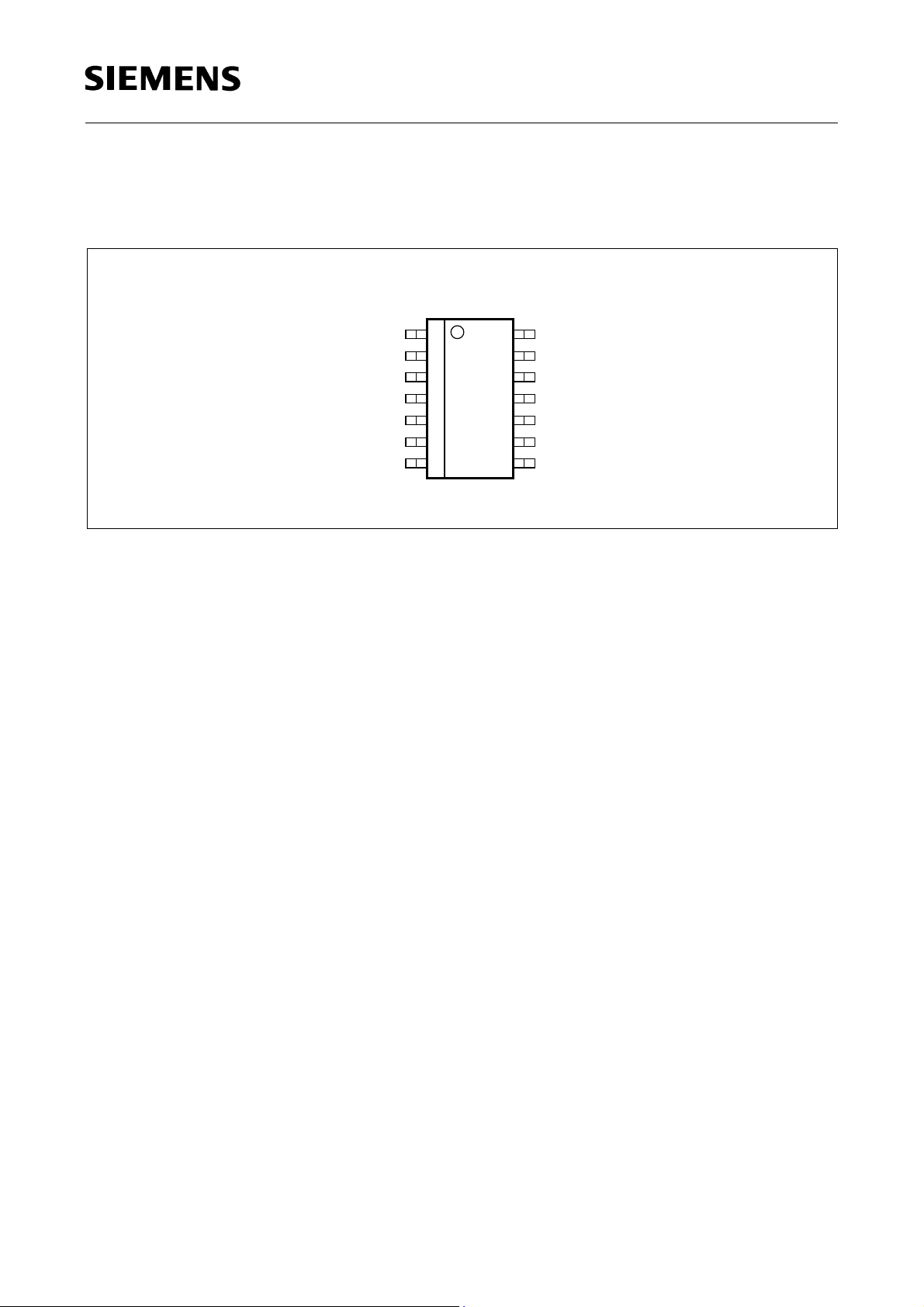
Pin Configuration
(top view)
TLE 6252 G
P-DSO-14-2
Figure 2
INH
TxD
RxD
NERR
NSTB
ENT
WAKE
13
12
11
10
9
87
V
BAT
GND
CANL
CANH
V
CC
RTL
RTH
AEP02411
114
2
3
4
5
6
Semiconductor Group 3 1998-11-01
Page 4
Table 1 Pin Definitions and Functions
Pin No. Symbol Function
1INHInhibit output;
For controlling an external 5 V regulator
2TxDTransmit data input;
LOW: bus is dominant, HIGH: bus is recessive
3RxDReceive data output;
LOW: bus is dominant
4 NERR Error flag output;
LOW: bus error
5 NSTB Not stand-by input;
Digital control signal for low power modes
TLE 6252 G
6ENTEnable transfer input;
Digital control signal for low power modes
7 WAKE Wake-up input;
If level of
V
changes the device initials a wake-up from
WAKE
sleep mode by switching INH HIGH
8RTHTermination resistor output;
For CANH line, controlled by internal failure management
9RTLTermination resistor output;
For CANL line, controlled by internal failure and mode
management
10
V
CC
Supply voltage;
+5 V
11 CANH Bus line H;
HIGH: dominant state, external pull-down for termination
12 CANL Bus line L;
LOW: dominant state, external pull-up for termination
13 GND Ground
14
V
BAT
Battery voltage;
+ 12 V
Semiconductor Group 4 1998-11-01
Page 5
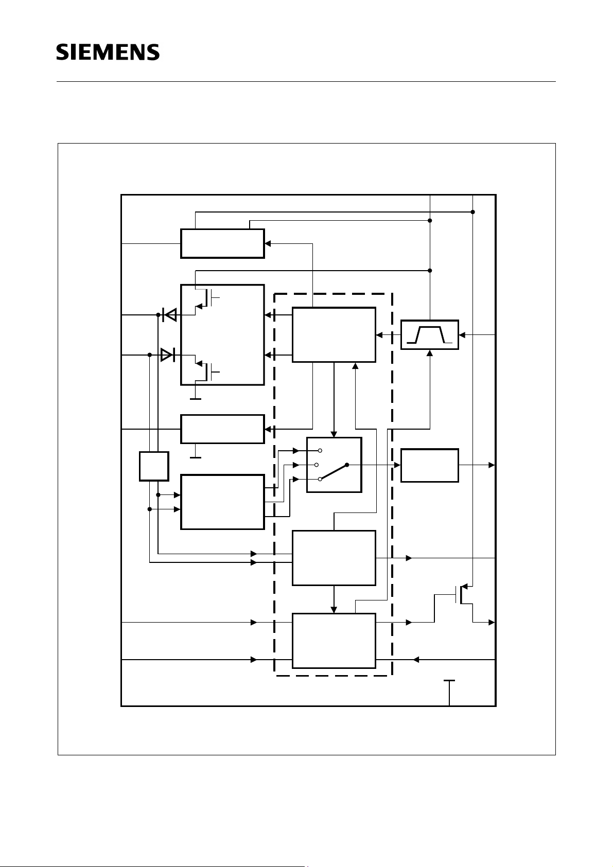
Functional Block Diagram
TLE 6252 G
RTL
CANH
CANL
RTH
9
11
12
8
Filter
L Termination
Driver
Temperature
Protection
H Termination
Failure
Management
V
CC
10
Output
Stage
V
BAT
14
2
TxD
3
RxD
Receiver
ENT
5
6
NSTB
Figure 3 Block Diagram
Failure Detect
Wake - Up
Time - Out
Stand - By
Sleep
Wake - Up
Contol Unit
13
GND
4
NERR
1
INH
7
WAKE
AEB02412
Semiconductor Group 5 1998-11-01
Page 6

TLE 6252 G
General Operation Modes
In addition to the normal operation mo de, the CAN transcei ver offers three mult iple l ow
power operation modes to save power when there is no bus achieved: sleep mode,
stand-by mode and VCC stand-by mode (see Table 2 and Figure 4). Via the control
inputs NSTB and ENT the operation modes are selected by the CAN controller.
In sleep operation mode the l owest power consumption is achieved. To deac tivate the
external voltage reg ulat or f or 5 V supply, th e INH output is swi tch ed to high impedance
in this mode. Also CANL is pull ed-up to the batt ery voltage via the RTL output and the
pull-up paths at input pins TxD and RxD are disabled from the internal supply.
On a wake-up request either by bus line activities or by the input WAKE, the transceiver
automatically switches on the voltage regulat or (5 V supply). The WAKE input reacts to
V
rising and falling edges. As soon as
is provided, the wake-u p request can be read
CC
on both the NERR and RxD outputs, upon which the microcontroller c an activate the
normal operation mode by setting the control inputs NSTB and ENT high.
V
Bat
V
In
NERR output in this mode is set l ow wh en the su pply vo ltage at pi n
-stand-by mode the wake up request is only reported at the RxD-output. The
CC
V
was below the
bat
battery voltage threshold of 1 V.
V
When entering the normal mode the
-Flag is reseted and the N ERR becomes h igh
bat
again.
V
In addition the
-Flag is set at a first connection of the device to battery voltage. This
bat
feature is usefull e.g. when c hanging the ECU an d therefore a pre setting routine of the
microcontroller has to be started.
If either of the supply voltage drop below the specified limits, the transceiver
automatically goes to a stand-by mode.
Semiconductor Group 6 1998-11-01
Page 7
TLE 6252 G
Table 2 Truth Table of the CAN Transceiver
NSTB ENT Mode INH NERR RxD RTL
V
00
stand-by
BAT
0 0 sleep mode
1)
V
bat
2)
floating switched
active LOW wa ke- up i nte rrupt if
V
is present
CC
switched
to V
V
to
BAT
BAT
0 1 go to sleep
command
10VCC stand-by
1 1 normal mode V
floating switched
3)
V
active LOW
bat
V
power-on
BAT
flag
bat
active LOW
error flag
active LOW
wake-up
interrupt
HIGH =
receive;
V
to
BAT
switched
to V
CC
switched
V
to
CC
LOW =
dominant
receive data
1)
Wake-up interrupts are releas ed w hen entering normal operation mo de.
2)
If go to sleep command was used before. ENT may turn LOW as VCC drops, without affecting internal functions.
3)
V
power-on flag will be reseted whe n ent ering normal operation mode.
BAT
Semiconductor Group 7 1998-11-01
Page 8
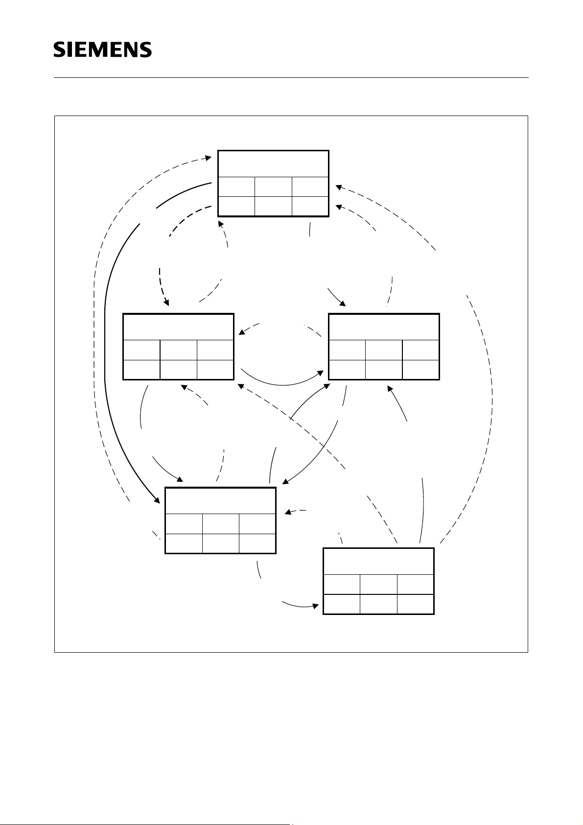
Normal Operation
TLE 6252 G
NSTB = 0
ENT =10
V
=
CC
V
CC
NSTB ENT INH
1
=
NSTB10
=ENT
NSTB = 1
V
=
CC
NSTB INH
1
0
NSTB
=
ENT11
=
V
CC
HIGH
NSTB =
ENT
V
CC
1
=0
=
1
Go to Sleep
ENT
1
ENT INH
11
NSTB
V
CC
NSTB
V
CC
=0ENT
tt
<
h
float.
HIGH
(NSTB = 0
ENT = 0)
V
CC
=1
1=
=00 or
=
or
=
ENT
V
CC
0
NSTB
0
=ENT 1
NSTB
V
CC
1
==1
V
BAT
1
==1
NSTB
ENT
V
CC
Stand-ByStand-By
ENT
00
==1
1
=1
NSTB
ENT
V
CC
==1
1
=1
INH
HIGH
(Wake-Up from
bus or via WAKE pin)
V
BAT
tt
>
WO
Sleep Mode
t>t
1=ENT
h
NSTB
0
ENT
0
INH
float.
AED02413
Figure 4 State Diagram
The transceiver will stay in a present operating mode until a suitable condition disposes
a state change. If not otherwise defin ed all conditions are AND-com bined. The signals
V
and V
CC
show if the supply is available (e.g. VCC = 1 : VCC voltage is present). If at
BAT
minimum one supply voltage is switched on, the start-up procedure begins (not figured).
After a delay time the device changes to normal operating or stand-by mode.
Semiconductor Group 8 1998-11-01
Page 9

TLE 6252 G
Bus Failure Management
The TLE 6252 detects the bus failures as de scribed in the fo llowing (Table 3, failures
listed according to ISO 11519-2) and automati cally switches to a dedicated CANH or
CANL single wire mode to maintain data transmission if necessary. Therefore, it is
equipped with one differential receiver and 4 single ended comparators, two for each bus
line. To avoid false triggering by external RF influences the single wire modes are
activated after a certain delay time. As soon as the bus failure disappears the transceiver
switches back to differential mode after another time delay. Bus failures are indicated in
the normal operation mode by setting the NERR output to LOW.
To reduce EMI the dynamic slopes of the CANL and CANH signals are both limited and
symmetric. This allows the use of an unshie lded twist ed or paral lel pair of wires for the
bus. During single-wire transmission the EMI performance of the system is degraded
from the differential mode.
The differential receiver threshold is set to – 2.8 V. This ensures correct reception in the
normal operation mode as well as in the failure cases 1, 2 and 4 with a noise margin as
high as possible. For these failures, further failure management is not necessary.
Detection of the failure cases 1, 2 and 4 is only possible when the bus is dominant.
Nevertheless, they are reported on the NERR output until transmission of the next CAN
word on the bus begins.
When one of the bus fai lures 3, 5, 6, 6a and 7 is detected, the defec tive bus wire is
disabled by switching off the affected bus termination and the respective output stage. A
wake-up from sleep mode via the bus is possible either via a dominant CANH or C ANL
line. This ensures that a wake-up is possible even if one of the failures 1 to 7 occurs.
In case the transmission data input, TxD from the CAN controller is permanently
dominant, both, the CANH and CANL transmitting stage, are deactiva ted after a delay
time. This is necessary to prevent blocking the bus by a defective protocol unit. The
transmit time out error is flagged on NERR.
Semiconductor Group 9 1998-11-01
Page 10

TLE 6252 G
Table 3 Specified Wiring Failure Cases on the Bus Line
(according to ISO 11519-2)
CANH CANL
Wire Interrupted
Failure case 2:
TxD
1
CANL
CANH
V
CC
GND
RxD
2
AES02414
Failure case 1:
TxD
1
Wire Short-Circuited to GND
Failure case 4:
V
CC
Failure case 5:
1)
CANL
CANH
V
CC
GND
V
CC
RxD
2
AES02415
TxD
CANL
1
RxD
2
TxD
1
CANH
GND
GND
AES02416
CANL
CANH
GND
GND
RxD
2
AES02417
Semiconductor Group 10 1998-11-01
Page 11

TLE 6252 G
Fail
V
V
Table 3 Specified Wiring Failure Cases on the Bus Line (cont’d)
(according to ISO 1151 9-2)
CANH CANL
Wire Short-Circuited to Battery
ure case 6:
Failure case 6a:
TxD
1
> 7.2
CANH
1.8 V < < 7.2 V (no ISO failure)
V
CANH
V
CC
CANL
RxD
2
CANH
V
BAT
GND
AES02418
Failure case 3:
Failure case 3a:
TxD
1
V
1.8 V < < 7.2 V (no ISO failure)
CANL
V
CANL
CANH
> 7.2 V
V
CANL
V
BAT
CC
GND
CANL Mutually Short-Circuited to CANH
1)
RxD
2
AES02419
V
Failure case 7:
CC
CANL
TxD
1
RxD
2
CANH
GND
1)
The images represent a communication between two participants of the network (see Figure 1). The controller
of the local area 1 transmits data (T×D
cases 1 to 7 occurs, the error handling enables communication th rough appreciated reactions.
) to the receiver of th e local area 2 (R×D2). When a single failur e of
1
AES02420
Semiconductor Group 11 1998-11-01
Page 12

TLE 6252 G
Circuit Protection
A current limiting circuit protects the CAN trans ceiver output stages from damage by
short-circuit to positive and negative battery voltages.
The CANH and CANL pins are protected again st electrical tra nsients which may occur
in the severe conditions of automotive environments.
The transmitter output s tage ge nera tes the majority of the p ower dissipation. Therefore
it is disabled if the jun ction temperature exceeds the maximum v alue. This effectively
reduces power dissipation, and hence will lead to a lower chip temperat ure, while other
parts of the IC can remain operating.
Absolute Maximum Ratings
Parameter Symbol Limit Values Unit Notes
min. max.
Input voltage at
Logic supply voltage
V
BAT
V
CC
Input voltage at TxD, RxD, NERR,
V
V
V
NSTD and ENT
Input voltage at CANH and CANL
Input voltage at CANH and CANL
V
V
Transient voltage at CANH and CANL V
Input voltage at WAKE V
Input current at WAKE
I
Input voltage at INH, RTH and RTL V
Termination resistances at RTL and
R
RTH
Junction temperature
Storage temperature
Electrostatic discharge voltage
T
T
V
at any pin
BAT
CC
IN
BUS
BUS
BUS
IN
IN
IN
RTL/H
j
stg
esd
– 0.3 40 V –
– 0.3 6 V –
– 0.3 V
+ 0.3 V –
CC
– 10 27 V –
– 40 40 V
– 150 100 V
– V
+ 0.3 V –
BAT
– 15 – mA
– 0.3 V
+ 0.3 V –
BAT
1)
2)
3)
500 16000 Ω –
– 40 150 °C–
– 55 155 °C–
– 4000 4000 V
4)
1)
V
= 0 to 5. 5 V; V
CC
2)
See ISO 7637
3)
Negative currents flowing out of the I C .
4)
Human body model: equivalent to discharging a 100 pF capacitor through a 1.5 kΩ resistor.
> 0 V; t < 0.1 ms; load dump
BAT
Note: Maximum ratings are absolute ratings; exceeding one of these values may cause
irreversible damage to the integrated circuit.
Semiconductor Group 12 1998-11-01
Page 13

TLE 6252 G
Operating Range
Parameter Symbol Limit Values Unit Notes
min. max.
Logic input voltage
Battery input voltage V
Junction temperature
Thermal Resistance
Junction ambient
V
T
R
CC
BAT
j
thja
4.75 5.25 V –
627 V–
– 40 150 °C–
–120 K/W–
Semiconductor Group 13 1998-11-01
Page 14

TLE 6252 G
Static Characteristics
V
4.75 V ≤
≤ 5.25 V; V
CC
otherwise specified). All voltages are defined with respect to ground. Positive current
flowing into the IC.
NSTB
= V
; 6 V ≤ V
CC
≤ 27 V; – 40 ≤ Tj≤ +125°C (unless
BAT
Parameter Symbol
V
Supplies
Supply current I
Supply current
V
stand-by)
(
CC
Supply current
V
stand-by)
(
BAT
Supply current
CC
, V
BAT
I
I
I
I
I
CC
CC
BAT
BAT
CC
BAT
+
+
(sleep operation mode)
Limit Values
Unit Notes
min. typ. max.
– 3.5 10 mA recessive;
TxD =
V
CC
operating mode
– 6 20 mA dominant;
TxD = 0 V; no load;
normal operating
mode
– 120 500 µA VCC = 5 V;
V
= 12 V;
BAT
T
< 90 °C
–55100µA
A
–1530µA VCC = 0 V;
V
= 12 V;
BAT
T
< 90 °C
A
; normal
Battery voltage for setting
V
BAT
––1.0VVCC stand-by mode
power-on flag
Battery voltage low time
t
pw(on)
–200–µs VCC stand-by mode
for setting power-on flag
Receiver Output R×D and Error Detection Output NERR
HIGH level output voltage
V
OH
(pin NERR)
HIGH level output voltage
V
OH
(pin RxD)
LOW level output voltage
Semiconductor Group 14 1998-11-01
V
OL
V
CC
– 0.9
V
CC
– 0.9
0–0.9VI0 = – 1.25 mA
–
–
V
V
CC
CC
V I0 = – 100 µA
V I0 = – 250 µA
Page 15

Static Characteristics (cont’d)
TLE 6252 G
4.75 V ≤
V
≤ 5.25 V; V
CC
NSTB
= V
; 6 V ≤ V
CC
≤ 27 V; – 40 ≤ Tj≤ + 125 °C (unless
BAT
otherwise specified). All voltages are defined with respect to ground. Positive current
flowing into the IC.
Parameter Symbol
Limit Values
Unit Notes
min. typ. max.
Transmission Input T×D, Not Stand-By NSTB and Enable Transfer ENT
HIGH level input voltage
threshold
LOW level input voltage
threshold
HIGH level input current
V
V
I
IH
IH
IL
0.7 ×
V
CC
– V
+ 0.3
CC
– 0.3 – 0.3 ×
V
CC
–920µA Vi = 4 V
V 500 mV hysteresis
V 500 mV hysteresis
(pins NSTB and ENT)
LOW level input current
I
IL
01–µA Vi = 1 V
(pins NSTB and ENT)
HIGH level input current
I
IH
– 200 – 50 – 25 µA Vi = 4 V
(pin TxD)
LOW level input current
(pin TxD)
Forced battery voltage
stand-by mode (fail safe)
Minimum hold time for
Go-To-Sleep command
Wake-up Input WAKE
Input current
Wake-up threshold
voltage
I
IL
V
CC
t
hSLP
I
IL
V
WK(th)
– 800 – 200 – 100 µA Vi = 1 V
2.75 – 4.5 V –
42238µs–
–3 –2 –1 µA–
2.03.04.0VV
NSTB
= 0 V
Semiconductor Group 15 1998-11-01
Page 16

Static Characteristics (cont’d)
TLE 6252 G
4.75 V ≤
V
≤ 5.25 V; V
CC
NSTB
= V
; 6 V ≤ V
CC
≤ 27 V; – 40 ≤ Tj≤ +125°C (unless
BAT
otherwise specified). All voltages are defined with respect to ground. Positive current
flowing into the IC.
Parameter Symbol
Limit Values
Unit Notes
min. typ. max.
Inhibit Output INH
HIGH level voltage drop
V
= V
∆
H
BAT
– V
INH
Leakage current
∆V
I
LI
H
–0.50.8VI
= – 0.18 mA;
INH
– 5 – 5.0 µA sleep operation
mode;
V
= 0 V
INH
Bus Lines CANL, CANH
Differential receiver
V
dRxD(rd)
–2.8 –2.5 –2.2 V VCC=5.0V
recessive-to-dominant
threshold voltage
Differential receiver
dominant-to-recessive
threshold voltage
CANH recessive output
voltage
CANL recessive output
voltage
CANH dominant output
voltage
CANL dominant output
voltage
CANH output current
V
dRxD(dr)
V
CANHr
V
CANLr
V
CANHd
V
CANLd
I
CANH
–3.17– 2.87–2.58V VCC=5.0V
0.10.20.3VTxD = VCC;
R
< 4 kΩ
RTH
V
CC
– 0.2
V
CC
– 1.4
––VTxD =
R
< 4 kΩ
RTL
–
V
CC
VTxD = 0 V;
normal mode;
I
= – 40 mA
CANH
V
CC
;
–1.11.4VTxD = 0 V;
normal mode;
I
= 40 mA
CAN
L
– 130 – 90 – 50 mA V
CANH
= 0 V;
TxD = 0 V
–0–µA sleep operation
mode;
V
CANH
= 12 V
Semiconductor Group 16 1998-11-01
Page 17

TLE 6252 G
Static Characteristics (cont’d)
V
4.75 V ≤
≤ 5.25 V; V
CC
otherwise specified). All voltages are defined with respect to ground. Positive current
flowing into the IC.
NSTB
= V
; 6 V ≤ V
CC
≤ 27 V; – 40 ≤ Tj≤ + 125 °C (unless
BAT
Parameter Symbol
CANL output current I
Voltage detection
CANL
V
det(th)
threshold for short-circuit
to battery voltage on
CANH and CANL
Voltage detection
V
det(th)
threshold for short-circuit
to battery voltage on
CANH
CANH wake-up voltage
V
WAKEH
threshold
Limit Values
Unit Notes
min. typ. max.
– 50 90 130 mA V
CANL
= 5 V;
TxD = 0 V
–0–µA sleep operation
mode;
V
V
CANL
BAT
= 0 V;
= 12 V
6.5 7.3 8.0 V normal operation
mode
V
BAT
– 2.5
V
BAT
–2
V
BAT
–1
V stand-by/
sleep operation
mode
1.21.92.7V–
CANL wake-up voltage
threshold
Wake-up voltage
threshold difference
CANH single-ended
receiver threshold
CANL single-ended
receiver threshold
CANH leakage current
V
WAKEL
V
∆
V
CANH
V
CANL
I
CANHl
WAKE
2.43.13.8V–
0.2––V∆V
V
SLP
SLPH
= V
SLPL
–
1.5 1.9 2.3 V failure cases 3, 5
and 7
2.8 3.1 3.8 V failure case 6 and
6a
–05µA VCC=0V,
V
=0V,
bat
V
R
T
=13.5V,
CANL
= 100 Ω,
RTL
<85°C
j
Semiconductor Group 17 1998-11-01
Page 18

TLE 6252 G
Static Characteristics (cont’d)
V
4.75 V ≤
≤ 5.25 V; V
CC
otherwise specified). All voltages are defined with respect to ground. Positive current
flowing into the IC.
NSTB
= V
; 6 V ≤ V
CC
≤ 27 V; – 40 ≤ Tj≤ +125°C (unless
BAT
Parameter Symbol
CANL leakage current I
CANLl
Termination Outputs RTL, RTH
RTL to
switch-on
CC
R
RTL
V
resistance
RTL output voltage
RTL to BAT switch series
V
R
oRTL
oRTL
resistance
Limit Values
Unit Notes
min. typ. max.
–05µA VCC= 0 V,
V
= 0 V,
bat
V
R
T
= 5 V,
CANH
=100Ω,
RTH
<85°C
j
–4395Ω Io =–10 mA;
normal operating
mode
V
V
CC
– 1.0
CC
– 0.7
10 16 35 kΩ V
–V|Io| < 1 mA; VCC
stand-by mode
stand-by or
BAT
sleep operation
mode
RTH to ground
switch-on
resistance
RTH output voltage
RTH pull-down current
RTL pull-up current
RTH leakage current
R
RTH
V
oRTH
I
RTHpd
I
RTLpu
I
RTHl
–4395Ω Io = 10 mA; normal
operating mode
–0.71.0VIo = 1 mA;
low power mode
–75–µA normal operating
mode, failure
cases 6 and 6a
–– 75–µA normal operating
mode, failure
cases 3, 3a, 5 and 7
–05µA VCC= 0 V,
V
= 0 V,
bat
V
R
T
= 5 V,
CANH
=100Ω,
RTH
<85°C
j
Semiconductor Group 18 1998-11-01
Page 19

Static Characteristics (cont’d)
TLE 6252 G
4.75 V ≤
V
≤ 5.25 V; V
CC
NSTB
= V
; 6 V ≤ V
CC
≤ 27 V; – 40 ≤ Tj≤ + 125 °C (unless
BAT
otherwise specified). All voltages are defined with respect to ground. Positive current
flowing into the IC.
Parameter Symbol
Limit Values
Unit Notes
min. typ. max.
RTL leakage current I
RTLl
–05µA VCC=0V,
V
=0V,
bat
V
R
T
=13.5V,
CANL
= 100 Ω,
RTL
<85°C
j
Thermal Shutdown
Shutdown junction
T
jSH
150 – –
o
C–
temperature
Semiconductor Group 19 1998-11-01
Page 20

TLE 6252 G
Dynamic Characteristics
V
= 4.75 V to 5.25 V; V
CC
otherwise specified). All voltages are defined with respect to ground. Positive current
flows into the IC.
Parameter Symbol Limit Values Unit Notes
NSTB
= V
CC
; V
= 6 V to 27 V; TA = – 40 to + 125 oC (unless
BAT
min. typ. max.
CANH and CANL bus
output transition time
recessive-to-dominant
CANH and CANL bus
output transition time
dominant-to-recessive
Minimum dominant time
for wake-up on CANL or
CANH
Minimum WAKE Low time
for wake-up
Failure cases 3 and 6
detection time
Failure case 6a detection
time
Failure cases 5, 6, 6a and
7 recovery time
t
rd
t
dr
t
wu(min)
t
WK(min)
t
fail
0.6 1.4 2.0 µs 10% to 90%;
C
= 10 nF;
1
C
= 0; R
2
= 100 Ω
1
0.7 1.0 1.3 µs 10% to 90%;
C
= 1 nF; C
1
R
= 100 Ω
1
= 0;
2
82238µs stand-by modes
V
= 12 V
BAT
20 36 60 µs Low power modes
V
= 12 V
BAT
30 55 80 µs normal operating
mode
2 4.8 8 ms normal operating
mode
30 55 80 µs normal operating
mode
Failure cases 3 recovery
time
Failure cases 5 and 7
detection time
Failure cases 5, 6, 6a and
7 detection time
Failure cases 5, 6, 6a and
7 recovery time
Semiconductor Group 20 1998-11-01
150 450 750 µs no rm al opera ting
mode
0.75 1.8 4.0 ms normal operating
mode
0.8 3.6 8.0 ms stand-by modes;
V
= 12 V
BAT
–2–µs stand-by modes;
V
= 12 V
BAT
Page 21

TLE 6252 G
Dynamic Characteristics (cont’d)
V
= 4.75 V to 5.25 V; V
CC
otherwise specified). All voltages are defined with respect to ground. Positive current
flows into the IC.
Parameter Symbol Limit Values Unit Notes
NSTB
= V
CC
; V
= 6 V to 27 V; TA = – 40 to + 125 oC (unless
BAT
min. typ. max.
Propagation delay
TxD-to-RxD LOW
(recessive to dominant)
t
PD(L)
–0.81.5µs C1 = 100 pF;
C
= 0;
R
2
= 100 Ω;
1
no failures and bus
failure cases 1, 2,
3a and 4
C
–0.81.5µs
= C2 = 3.3 nF;
1
R
= 100 Ω; no bus
1
failure and failure
cases 1, 2, 3a and
4
C
–1.21.8µs
100 pF; C2 = 0;
1
R
= 100 Ω; bus
1
failure cases 3, 5,
6, 6a and 7
C
–1.21.8µs
= C2 = 3.3 nF;
1
R
=100 Ω; bus
1
failure cases 3, 5,
6, 6a and 7
Semiconductor Group 21 1998-11-01
Page 22

TLE 6252 G
Dynamic Characteristics (cont’d)
V
= 4.75 V to 5.25 V; V
CC
otherwise specified). All voltages are defined with respect to ground. Positive current
flows into the IC.
Parameter Symbol Limit Values Unit Notes
NSTB
= V
CC
; V
= 6 V to 27 V; TA = – 40 to + 125 oC (unless
BAT
min. typ. max.
Propagation delay
TxD-to-RxD HIGH
(dominanat to recessive)
t
PD(H)
–1.52.0µs C1 = 100 pF;
C
= 0;
R
2
=100 Ω;
1
no failures and bus
failure cases 1, 2,
3a and 4
C
–2.53.0µs
= C2 = 3.3 nF;
1
R
= 100 Ω; no bus
1
failure and failure
cases 1, 2, 3a and
4
C
–1.01.5µs
100 pF; C2 = 0;
1
R
= 100 Ω; bus
1
failure cases 3, 5,
6, 6a and 7
C
–1.42.1µs
= C2 = 3.3 nF;
1
R
= 100 Ω; bus
1
failure cases 3, 5,
6, 6a and 7
Minimum hold time to go
t
h(min)
42238µs–
sleep command
Edge-count difference
(falling edge) between
n
e
–4––normal operating
mode
CANH and CANL for
failure cases 1, 2, 3a and 4
detection NERR becomes
LOW
Edge-count difference
–2––
(rising edge) between
CANH and CANL for
failure cases 1, 2, 3a and 4
recovery
TxD permanent dominant
t
TxD
1 2.5 4 ms normal mode
disable time
Semiconductor Group 22 1998-11-01
Page 23

Test and Application
+ 5 V
73654 21
RxDNERR TxDENTWAKE NSTB INH
TLE 6252
CAN Transceiver
RTH RTL CANH CANL GND
V
CC
V
BAT
141312111098
TLE 6252 G
20 pF
+ 12 V
R
11
CC
2
CAN Bus Substitute 1
R R
1
C
K
R
C
11
R
= 100
1
C
1
C
K
1,2
C
K
Ω
= 10 nF
= 1 nF
Schaffner
Generator
CAN Bus Substitute 2
AES02423
Figure 5 Test Circuits
For isolated testing the CAN Bus Substitute 1 is connected to the CAN Transceiver (see
C
Figure 5). The capacitors
R
termination resistors
RTH
and R
simulate the cable. Allowed minimum values of the
1-3
are 500 Ω. Electro mag netic interference on the bus
RTL
lines is simulated by switching to CAN Bus Substitute 2. The waves of the applied
transients will be in accordance with ISO 7637 part 1, test 1, test pulses 1, 2, 3a and 3b.
Semiconductor Group 23 1998-11-01
Page 24

V
TLE 6252 G
BAT
C 505C / C 515C / C 164CJ
Microcontroller with On - Chip CAN Module
7
6
5
WAKE ENT NSTB
4
NERR
RxD
2
3
TxD
INH
TLE 6252
CAN Transceiver
RTH
8
R
RTL
RTH
V
CANH
CC
9
10
R
RTL
CANL
11
GND
12
V
13
100 nF
1
BAT
14
+5 V
100 nF
TLE 4271 / TLE 4276
Low Drop Voltage Regulator
µ
22 F
CAN Bus Line
AES02422
Figure 6 Application of the TLE 6252 G
Semiconductor Group 24 1998-11-01
Page 25

Package Outlines
P-DSO-14-2
(Plastic Dual Small Outline)
-0.1
0.2
-0.2
1.45
4
-0.2
1.75 max
TLE 6252 G
0.35 x 45˚
1)
+0.06
0.19
0.35
1.27
+0.15
2)
0.1
0.2 14x
±0.2
6
0.4
+0.8
8˚ max.
14 8
17
8.75
-0.2
1)
Index Marking
1) Does not include plastic or metal protrusion of 0.15 max. per side
2) Does not include dambar protrusion of 0.05 max. per side
GPS05093
Sorts of Packing
Package outlines for tubes, trays etc. are contained in our
Data Book “Package Information”.
SMD = Surface Mounted Device
Semiconductor Group 25 1998-11-01
Dimensions in mm
 Loading...