

3-A DC Motor Driver
TLE 5203
Overview SPT IC
Features
• Output current ± 3 A
• I/O error diagnostics
• Short-circuit proof
• Four-quadrant operation
• Integrated free-wheeling diodes
• Wide temperature range
• Open load detection
• Break low, if break high required, the device
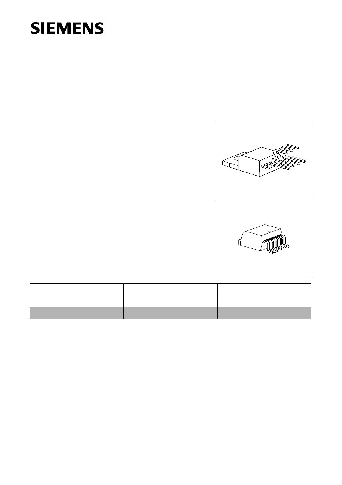
P-TO220-7-1
TLE 5204 will fit
1)
P-TO220-7-8
Type Ordering Code Package
TLE 5203 Q67000-A9096 P-TO220-7-1
TLE 5203 G Q67006-A9242 P-TO220-7-8
Description
TLE 5203 is an integrated power bridge with DMOS output stages for driving DC motors.
This motor bridge is optimized for driving DC motors in reversible operation. The internal
protective circuitry in particular ensures that no crossover currents can occur.
Because the free-wheeling diodes are integrated, the external circuitry that is necessary
is reduced to the capacitors on the supply voltage.
The control inputs have TTL/CMOS-compatible levels.
1)
SIEMENS Power Technology
Semiconductor Group 1 1998-02-01
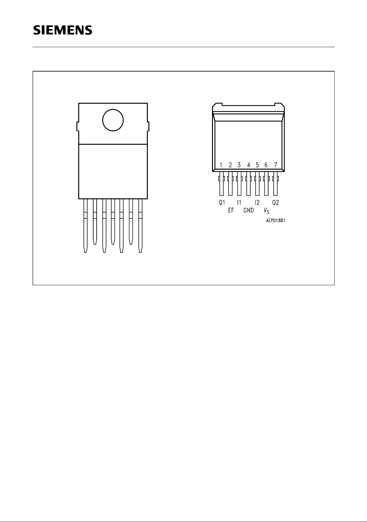
TLE 5203
TLE 5203 GTLE 5203
4321567
EF
Q1
Ι
1
GND
Ι
2
V
S
Q2
AEP01224
Figure 1 Pin Configuration (top view)
Semiconductor Group 2 1998-02-01

TLE 5203
Pin Definitions and Functions
Pin No. Symbol Function
1Q1Output of channel 1; Short-circuit proof, free-wheeling
diodes integrated for inductive loads
2EFError flag; TTL/CMOS-compatible output for error detection
(open drain)
3 I1 Control input 1; TTL/CMOS-compatible
4GNDGround; connected internally to cooling fin
5 I2 Control input 2; TTL/CMOS-compatible
6
V
S
Supply voltage; wire with capacitor matching load
7Q2Output of channel 2; Short-circuit proof, free-wheeling
diodes integrated for inductive loads
Circuit Description
Input Circuit
The control inputs consist of TTL/CMOS-compatible Schmitt triggers with hysteresis.
Buffer amplifiers are driven by these stages and convert the logic signal into the
necessary form for driving the power output stages.
Output Stages
The output stages form a switched H-bridge. Protective circuits make the outputs shortcircuit proof to ground and to the supply voltage throughout the operating range. Positive
and negative voltage s pikes, wh ich occur when switchin g inductive loads, are clamped
by integrated power diodes.
Semiconductor Group 3 1998-02-01

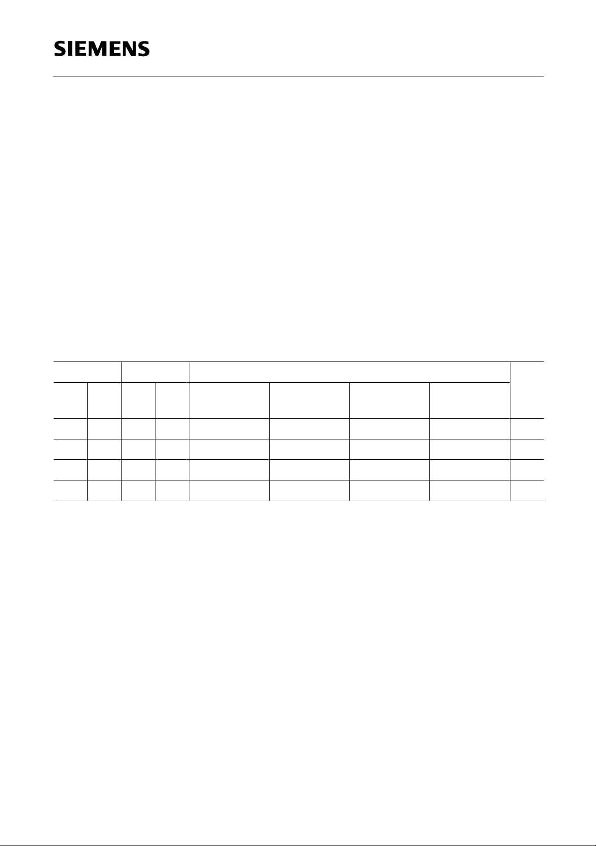
Functional Truth Table
E1 E2 Q1 Q2 Comments
L L H L Motor turns counterclockwise
L H L H Motor turns clockwise
HLLLBrake; both low side transistors turned-ON
H H Z Z Open circuit detection
Notes for Output Stage
Symbol Value
L Low side transistor is turned-ON
High side transistor is turned-OFF
H High side transistor is turned-ON
Low side transistor is turned-OFF
TLE 5203
Z High side transistor is turned-OFF
Low side transistor is turned-OFF
Monitoring Functions
An internal circuit ensures that all output transistors are turned-OFF if the supply voltage
is below the operating range.
A monitoring circuit for each output transistor detects whether the particular transistor is
active and in this case prevents the corresponding source transistor (sink transistor) from
conducting in sink operat ion (source operation). Therefore no crossover currents can
occur. Pulse-width operation is possible up to a maximum switching frequency of 1 kHz
for any load.
Depending on the load current higher frequencies are possible.
Protective Function
V
Various errors like short-circuit to +
, ground or across the load are detected. All faults
S
result in turn-OFF of the output stages after a delay of 40 µs and setting of the error flag
EF to ground. Changing the inputs resets the error flag.
Output Shorted to Ground Detection
If a high side transistor is switched on and its output is shorted to ground, the output
current is limited to typ 8 A. After a delay of 40 µs all outputs will be switched off and the
error flag EF is set to ground.
Semiconductor Group 4 1998-02-01
TLE 5203
Output Shorted to + VS and Overload Detection
An internal circuit detects if the current through the low side transistor is higher than 4 A
typ. In this case all outputs are turned off after 40 µs and the error flag EF is set to
ground.
At a junction temperature higher than 160 °C th e thermal shutdown turns off, all four
output stages commonly and the error flag is set without a delay.
Open Load Detection
The output Q1 has a 10 kΩ pull-up resi stor and the output Q 2 has a 10 kΩ pull-down
resistor. If E1 and E2 a re high, all o utput power s tages are turne d-OFF. In case of no
V
load between Q1 and Q2 the output voltage Q1 is
be detected by two comparators and an error flag will be set after a delay time of 40 µs.
Changing the inputs resets the error flip flop.
and Q2 is ground. This state wil l
S
Diagnosis
Input Output Diagnosis EF
E1 E2 Q1 Q2 Shorted
to GND
Shorted
V
to
S
Overload Open Load
L L H L Q1 Q2 X –L
L H L H Q2 Q1 X – L
HLLL– Q1, Q2 – – L
HHZZ–––XL
Semiconductor Group 5 1998-02-01
TLE 5203
V
=
EH
Pull Up
Ω10 k
EF
Pull
Down
10 kΩ
=
V
EL
&
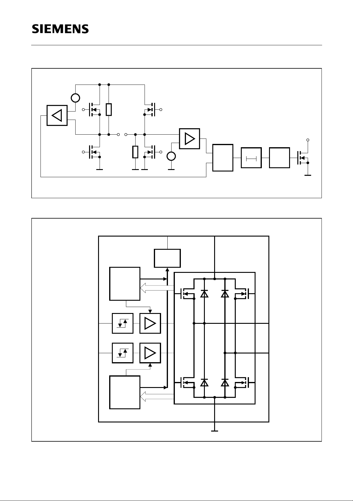
Figure 2 Simplified Schematic for Open Load Detection
Control Input 1
Error Flag
2
Error
Flag
Protection
Circuit 1
3
V
S
6
40 sµ
1
Output 1
RS
FF
AES01688
Control Input 2
5
7
Output 2
Protection
Circuit 1
4
GND
AEB01225
Figure 3 Block Diagram
Semiconductor Group 6 1998-02-01
 Loading...