

Siemens TLE4261S, TLE4261G, TLE4261 Datasheet
TLE 4261
5-V Low-Drop Voltage Regulator
Features
● Very low-drop voltage
● Very low quiescent current
● Low starting-current consumption
● Proof against reverse polarity
● Input voltage up to 42 V
● Overvoltage protection up to 65 V (≤ 400 ms)
● Short-circuit proof
● External setting of reset delay
● Integrated watchdog circuit
● Wide temperature range
● Overtemperature protection
● Suitable for automotive use
● EMC proofed (100 V/m)
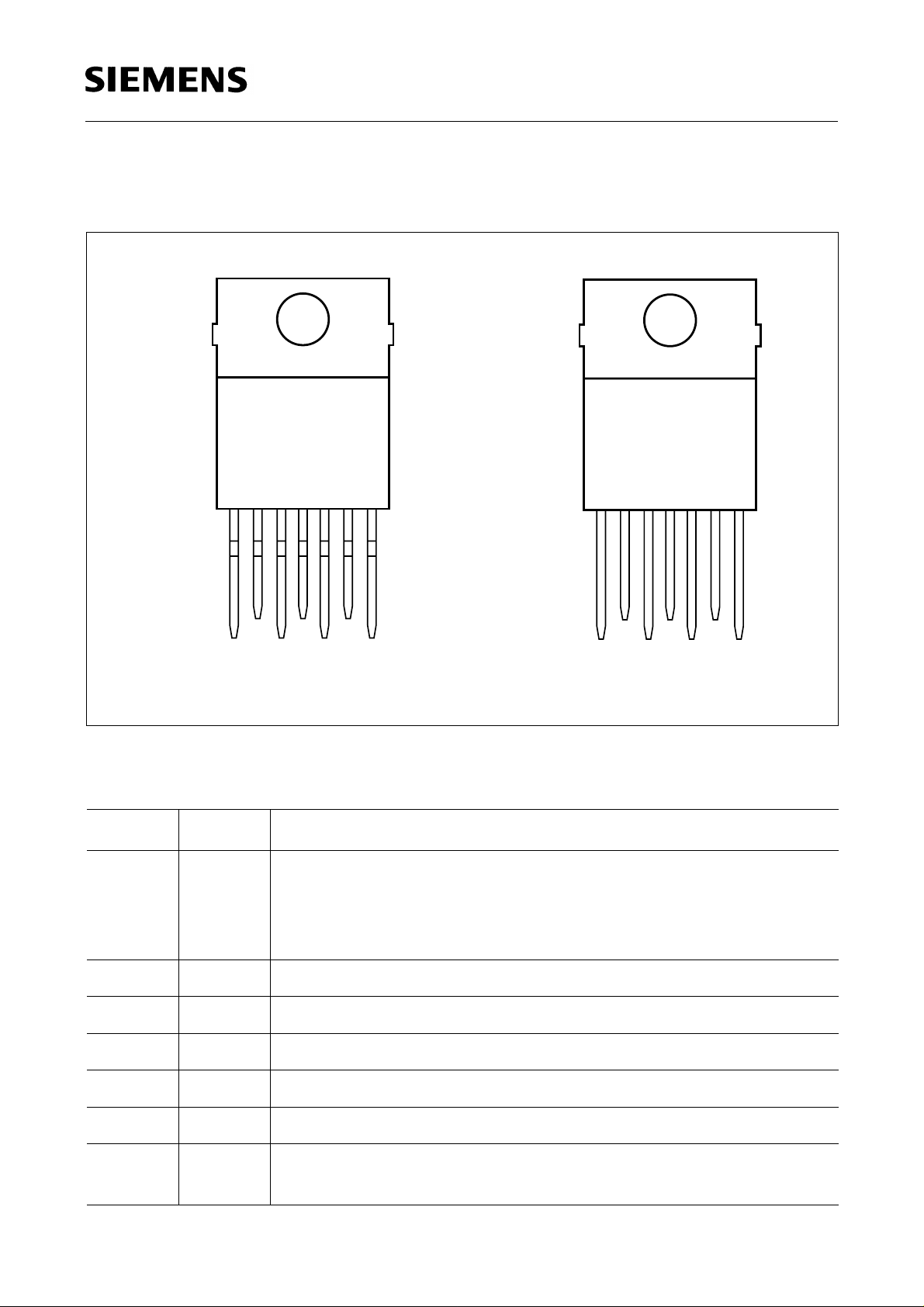
TLE 4261
Bipolar IC
P-TO220-7-1
P-TO220-7-2
Type Ordering Code Package
TLE 4261 Q67000-A9003 P-TO220-7-1
▼
TLE 4261 S Q67000-A9109 P-TO220-7-2
▼
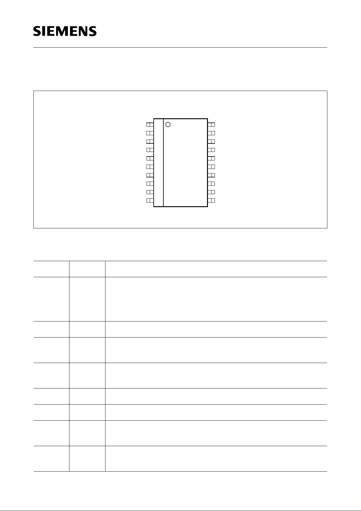
TLE 4261 G Q67000-A9059 P-DSO-20-6 (SMD)
▼
Please also refer to the new pin compatible
▼
device TLE 4271
P-DSO-20-6
Functional Description
TLE 4261 is a 5-V low-drop volta ge regulator in a P-TO220-7 or i n a P-DSO package.
The maximum input voltage is 42 V (65 V/≤ 400 ms). The device can produce an output
current of more than 500 mA. It is short-circuit proof and incorporates temperature
protection that disables the circuit at impermissibly high temperatures.
Semiconductor Group 1 1998-11-01

TLE 4261
Application Description
V
The IC regulates an input voltage
reset signa l is generat ed for a maxim um output voltage of
in the range VI = 6 V to 40 V to V
I
V
less than 4.75 V. The reset
Q
delay can be set ext ernally with a capacitor. A con nected micr oprocessor is moni tored
by the integrated watchdog c ircu it. Connecting this input to the input vol tage make s the
watchdog function inactive. The presence of a voltage less than 2 V on inhibit input
disables the regulator. The current consumption drops to max. 50 µA.
Design Notes for External Components
C
The input capacitor
causes a low-resista nt powerline and limits the rise ti mes of the
I
input voltage. The IC is protected against rise times up to 100 V/µs. It is possible to damp
the tuned circuit consisting of supply inductance and input capacitance with a resistor of
C
approx. 1 Ω in series to
.
I
The output capacitor maintains the stability of the regulating loop. Stability is guaranteed
with a rating of 22 µF at an ESR of 3 Ω max. in the operating temperature range.
= 5.0 V. A
Qrated
Circuit Description
The control amplifier compares a reference voltage, which is kept highly accurate by
resistance adjustment, to a voltage that is proportional to the output voltage and controls
the base of the series PNP transistor via a buffer. Saturation control as a function of the
load current prevents any over-saturation of the power element. If the output voltage
drops below 95.5 % of its typical value for more than 2 µs, a reset signal is triggered on
pin 3 and an external capacitor is discharged on pin 5. The reset signal is not cancelled
V
until the voltage on the capacito r has exceeded the upper switchi ng threshold
DT
. A
positive-edge-triggered watchdog circuit monitors the connected microprocessor and
will likewise trigger a reset if puls es are missing . The IC can be disa bled by a low le vel
on the inhibit input and the current consumption drops to < 50 µA.
The IC also incorporates a number of circuits for protection against:
● Overload
● Overvoltage
● Overtemperature
● Reverse polarity
Semiconductor Group 2 1998-11-01
Pin Configuration
(top view)
TLE 4261
TLE 4261
INH
V
QRES
Ι
4321567
GND
Watch
DRES
V
Q
AEP00592
TLE 4261 S
INH
QRES
V
Ι
4321567
GND
Watch
DRES
V
Q
AEP01181
Pin Definitions and Functions (TLE 4261; S)
Pin Symbol Function
1
V
I
Input voltage; block a capacitor directly to ground on the IC. The
capacitor rating will depend on the vehicle electrical system.
Oscillation of the input voltage can be damped by a resistor of
approx. 1 Ω in series with the input capacitor.
2INHInhibit; switches off the IC when low.
3QRESReset output; open-collector output controlled by the rese delay.
4GNDGround
5DRESReset delay; wired to ground using a capacitor.
6WatchWatchdog; monitors the microprocessor when active.
7
V
Q
5-V output voltage; block to ground using a capacitor of ≥ 22 µF.
ESR is ≤ 3 Ω in the operating temperature range.
Semiconductor Group 3 1998-11-01
Pin Configuration
(top view)
TLE 4261
TLE 4261 G
N.C.
N.C.
QRES
GND
GND 5
GND
N.C.
DRES
N.C.
1
2
3
4
6
7
8
9
10
AEP01182
Pin Definitions and Functions (TLE 4261 G)
Pin Symbol Function
18
V
I
Input voltage; block a capacitor directly to ground on the IC. The
capacitor rating will depend on the vehicle electrical system.
Oscillation of the input voltage can be damped by a resistor of
approx. 1 Ω in series with the input capacitor.
20
19
18
17
16
15
14
13
12
11
INH
N.C.
V
Ι
GND
GND
GNDGND
GND
N.C.
V
Q
Watch
20 INH Inhibit; switches off the IC when low.
3QRESReset output; open-collector output controlled by the reset
delay.
4 - 7
GND Ground; internally connected with pins 14 to 17.
14 - 17
9 DRES Reset delay; wired to ground using a capacitor.
11 Watch Watchdog; monitors the microprocessor when active.
12
V
Q
5-V output voltage; block to ground using a capacitor of ≥ 22 µF.
ESR is ≤ 3 Ω in the operating temperature range.
1, 2, 8, 10,
N.C. Not connected
13, 19
Semiconductor Group 4 1998-11-01
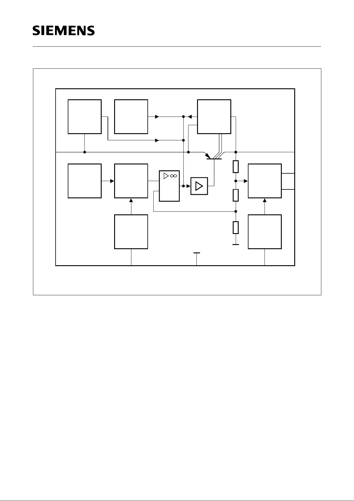
TLE 4261
Overvoltage
Monitoring
1
Input
(18)
Adjustment
Numbers in parentheses f or T LE 4261 G
Temperature
Sensor
BANDGAP
Reference
Inhibit
2(20)
Inhibit GND Watchdog
Control
Amplifier
+
-
(4-7)
Saturation
Control and
Protection
Buffer
RESET
Generator
Watchdog
(11) 64(14-17)
7
(12)
5
(9)
3
(3)
AEB00002
Output
RESET
Delay
RESET
Output
Block Diagram
Semiconductor Group 5 1998-11-01
TLE 4261
Absolute Maximum Ratings
T
= – 40 to 150 °C
j
Parameter Symbol Limit Values Unit Remarks
min. max.
Input
Input voltage
Input voltage
Input current
Inhibit
Voltage
Current
Reset Output
Voltage
Current
Ground
Current
Reset Delay
V
V
I
I
V
I
2
V
I
R
I
GND
I
I
–42
–
–
2
–0.3
–
R
– 0.3
–
45
65
1.6
42
5
42
–
V
V
A
V
mA––
V
–
–
t ≤ 400 ms
–
–
limited internally
–0.5A–
Voltage
Current
V
I
D
D
–0.3
–
42
–
V
–
–
limited internally
Watchdog
Voltage
V
W
–0.3 V
I
V–
Output
V
I
– V
I
Q
Differential voltage
Current
Semiconductor Group 6 1998-11-01
Q
–5.25
–
V
I
1.4
V
A
–
–
 Loading...