

1-A DC Motor Driver for Servo Driver Applications
Overview
Features
• Optimized for headlight beam control applic atio ns
• Current-peak-blanking (no electrolytic capacitor at
• Delivers up to 0.8 A continuous
• Low saturation voltage
; typ.1.2 V total @ 25 °C; 0.4 A
• Output protected against short circuit
• Overtemperature protection with hysteresis
• Over- and undervoltage lockout
• No crossover current
• Internal clamp diodes
• Enhanced power packages
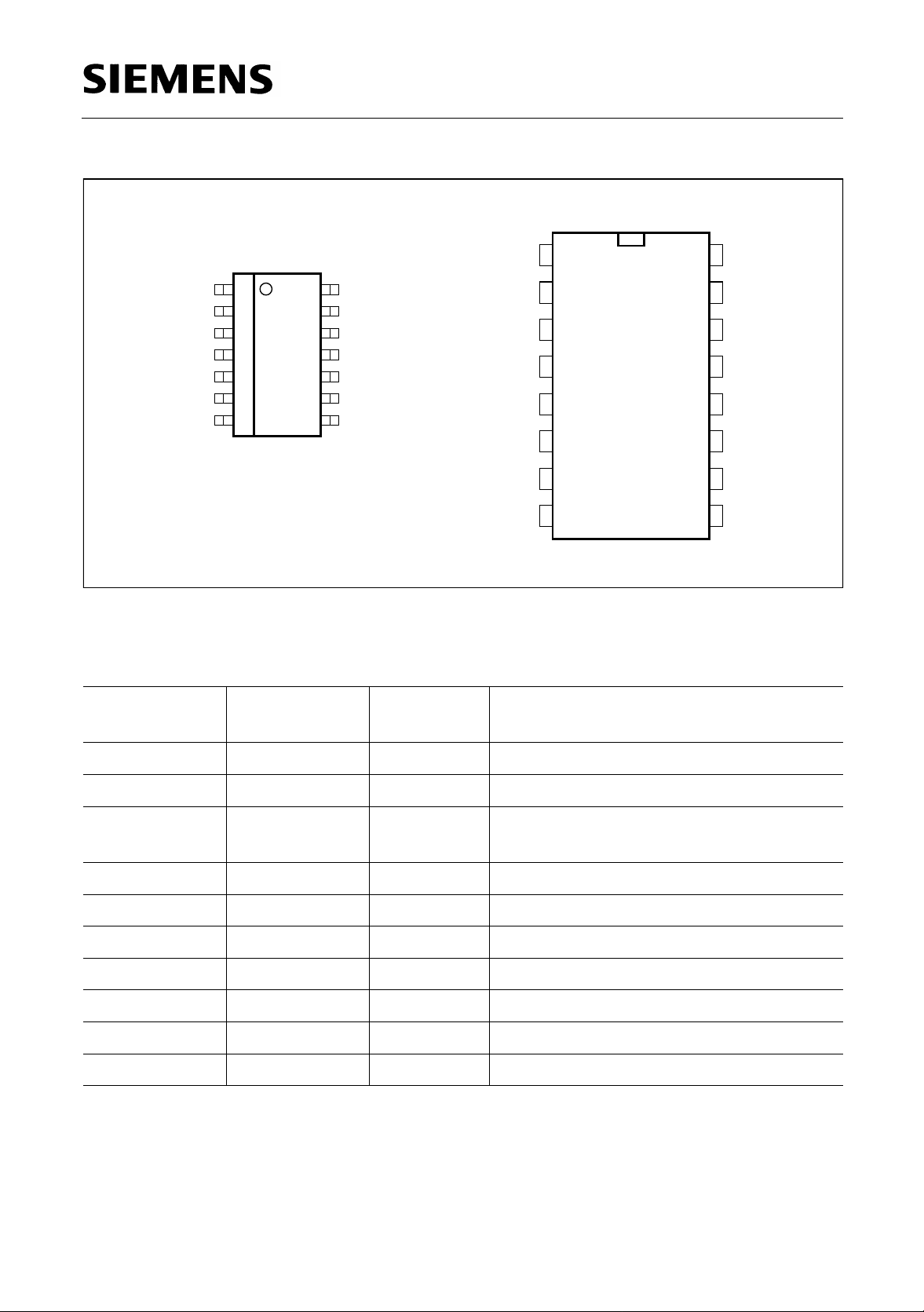
Type Ordering Code Package
V
)
S
TLE 4206
P-DIP-16-5
TLE 4206 Q67000-A9303 P-DIP-16-5
TLE 4206 G Q67006-A9299 P-DSO-14-4
P-DSO-14-4
Description
The TLE 4206 is a fully p rotected H-Bridge Driv er designed speci fically for automot ive
headlight beam control and industrial servo control applications.
The part is built using the Siemens bipolar high voltage power technology DOPL.
The standard enhanced power P-DSO-14 package meets the app licatio n requireme nts
and saves PCB-board space and costs. A P-DIP-16 package is also available.
The servo-loop-parameter pos.- and neg. Hysteresis, pos.- and neg. deadband and
angle-amplification are programmable with external resitors.
An internal window-comp arator controls the input line. In the case of a fault condition,
like short circuit to GND, short circuit to supply-voltage, and broken wire, the
TLE 4206 stops the motor immediately (brake condition).
V
The “programable current-peak-blank ing” d isa bles the s ervo - loop durin g the
voltage
S
drop caused by the stall current spi ke. So there is no need of an electrolytic blocking
V
capacitor at the
-terminal.
S
Furthermore the built in features like over- and undervoltage-lockout, short-circuitprotection and over-tempera ture-protection will open a wide range of automotiv e- and
industrial applications.
Semiconductor Group 1 1998-02-01
TLE 4206
P-DSO-14-4 P-DIP-16-5
FB
HYST
GND
GND
GND
OUT1
CPB
1
2
3
4
5
6
7
14
13
12
11
10
9
8
AEP02261
REF
RANGE
GND
GND
GND
OUT2
V
S
Figure 1 Pin Configuration (top view)
Pin Definitions and Functions
Pin No.
P-DSO-14-4
Pin No.
P-DIP-16-5
Symbol Function
FB
1
HYST
N.C.
GND
GND GND
GND GND
OUT1
CPB
2
3
4
5
6
7
8
AEP02262
16
15
14
13
12
11
10
9
REF
RANGE
N.C.
GND
OUT2
V
S
1 1 FB Feedback Input
2 2 HYST Hysteresis I/O
3, 4, 5,
10, 11, 12
4, 5, 6,
11, 12, 13
GND Ground
6 7 OUT1 Power Output 1
78CPB Current Peak Blanking Input
89
V
S
Power Supply Voltage
9 10 OUT2 Power Output 2
13 15 RANGE Range Input
14 16 REF Reference Input
3, 14 N.C. Not connected
Semiconductor Group 2 1998-02-01
TLE 4206
V
S
TLE 4206G
8
RANGE
REF
FB
HYST
13
14
1
2
Range-
AMP
Servo-
AMP
Hyst-
AMP
Protection
and Logic
HalfBridge
HalfBridge
6
OUT1
9
OUT2
3,4,5,
7
CPB
10,11,12
GND
AEB02258
Figure 2 Block Diagram (Pin numbers are valid for TLE 4206 G in P-DSO-14-4)
Semiconductor Group 3 1998-02-01
Absolute Maximum Ratings
Parameter Symbol Limit Values Unit Remarks
min. max.
Voltages
TLE 4206
Supply voltage
Supply voltage
Logic input voltages
(FB, REF, RANGE, HYST,
CPB)
Currents
Output current (OUT1, OUT2)
Output current (Diode)
Input current
(FB, REF, RANGE, HYST)
Temperatures
Junction temperature
Storage temperature
V
V
V
I
OUT
I
OUT
I
IN
T
T
S
S
I
j
stg
– 0.3 45 V –
– 1 – V t < 0.5 s; IS > – 2 A
– 0.3 20 V –
– – A internally limited
–1 1 A –
– 2
– 6
2
6
mA
mA
t < 2 ms; t/T < 0.1
– 40 150 °C–
– 50 150 °C–
Thermal Resistances
Junction pin
R
thj-pin
– 25 K/W measured to pin 5
(P-DSO-14-4)
Junction ambient
R
thjA
–65K/W–
(P-DSO-14-4)
Junction pin
R
thj-pin
– 15 K/W measured to pin 5
(P-DSO-16-5)
Junction ambient
R
thjA
–60K/W–
(P-DSO-16-5)
Note: Maximum ratings are abso lute ratings; exceeding any one of thes e values may
cause irreversible damage to the integrated circuit.
Semiconductor Group 4 1998-02-01
Operating Range
Parameter Symbol Limit Values Unit Remarks
min. max.
TLE 4206
Supply voltage
Supply voltage increasing
Supply voltage decreasing
Output current
Input current (FB, REF)
Junction temperature
V
S
V
S
V
S
I
OUT1-2
I
IN
T
j
818VAfter V
above
– 0.3 V
– 0.3 V
UV ON
UV OFF
V Outputs in tristate
V Outputs in tristate
– 0.8 0.8 A –
– 50 500 µA–
– 40 150 °C–
rising
S
V
UV ON
Semiconductor Group 5 1998-02-01
 Loading...