

2-A DC Motor Driver
Overview
Features
• Drives motors up to 2 A
• Integrated free-wheeling diodes 2.5 A
• Short-circuit proof to ground
• Overtemperature protection
• Low saturation voltages through bootstrap
• Wide temperature range
• Suitable for applications in automotive engineering
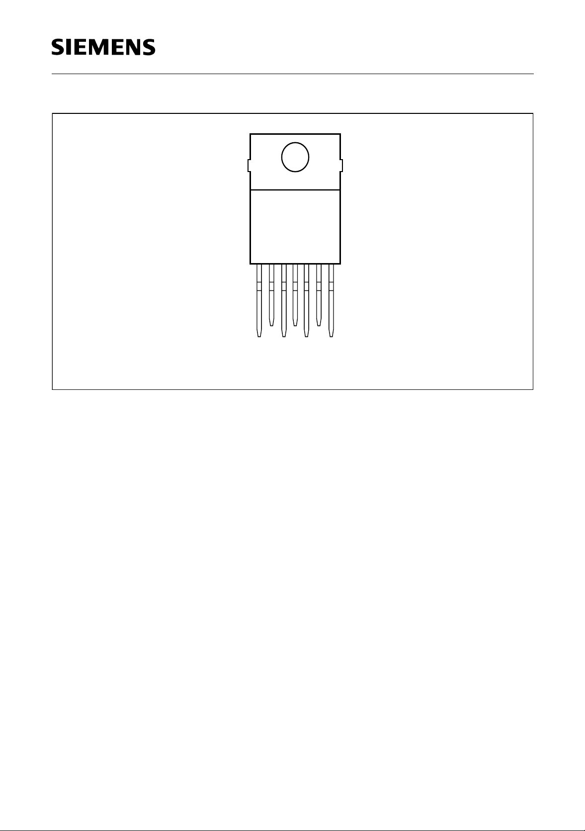
TLE 4202 B
Bipolar IC
P-TO220-7-1
Type Ordering Code Package
TLE 4202 B Q67000-A8225 P-TO220-7-1
Description
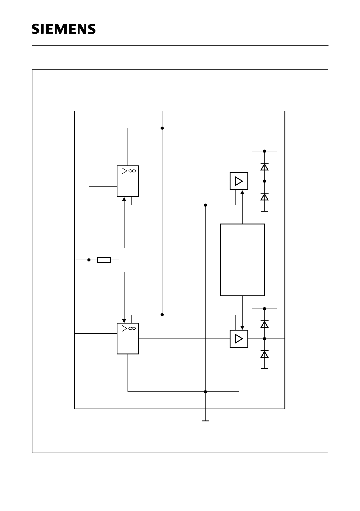
The two power comparators can swit ch magnet s, motors or oth er loads eith er by being
separated from each other or by being combined to a full-bridge circuit. The IC is
designed for application in motor vehicles. It can be applied at package temperatures
between – 40 °C and 130 °C.
The IC contains two amplifiers featuring a typical open-loop voltage gain of 80 dB at
500 Hz.
The input stages are PNP differential amplifiers thus resulting in a c omm on-mo de in put
V
voltage range from 0 V to approx . the value of
V
voltage of
. To obtain low saturation voltages at the sink circuit, the drive circuit of the
S
and in a maximum input differential
S
sink transistor is connected to the supply voltage. An SOA protective circuit protects the
IC against ground short-circuits. At chip temperatures above approx. 160 °C the source
transistors are turned off.
Semiconductor Group 1 1998-02-01
TLE 4202 B
4321567
Ι
12
Ι
Figure 1 Pin Configuration (top view)
3Q1GND
Q2
V
S
Ι
AEP00612
Semiconductor Group 2 1998-02-01
Pin Definitions and Functions
Pin No. Symbol Function
1I1Input 1
Non-inverting input 1, to be connected to pin 2 and pin 3
according to general rules
2I3Inverting input 3
Inverting inputs of the two comparators; internally connected to
reference voltage across 50 kΩ (typ. 1.7 V)
3Q1Output Q1
Push-pull output B DC-short-circuit proof to ground. Integrated
free-wheel diodes to ground and to supply voltage
4GNDGround
TLE 4202 B
5Q2Output Q2, see pin 3
6
V
S
Supply voltage
Has to be blocked to ground with a ceramic capacitor of at least
100 nF directly at the pins of the ICs
7I2Input 2
Non-inverting input 2; see pin 1
Semiconductor Group 3 1998-02-01
TLE 4202 B
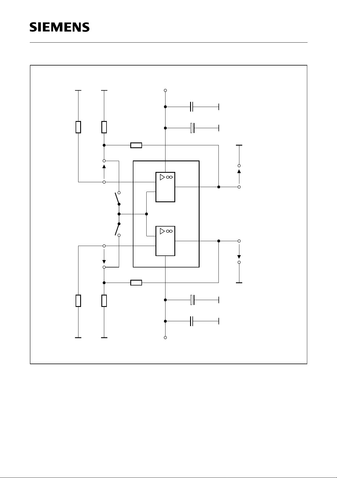
Input
1
Ι
Inverting
3
Ι
Input
Supply Voltage
V
S
6
V
S
80 dB
0 dB
1
+
Amp 1
-
3
Output Q1
Power
2
50 kΩ
+1.7 V
TLE 4202B
Limiter
and
Temperature
Protection
Input
7
2
Ι
+
-
Figure 2 Block Diagram
2Amp
80 dB
4
GND
0 dB
V
S
AEB00613
5
Output Q2
Semiconductor Group 4 1998-02-01
TLE 4202 B
Absolute Maximum Ratings
T
= – 40 to 130 °C
C
Parameter Symbol Limit Values Unit
min. max.
Supply voltage
Output current of
sink transistors
T
≤ 85 °C
C
Output current of
source transistors
internally limited
Diode peak currents
V
to +
S
to ground
Voltage at
pins I1, I2, I3
Voltage at
pins Q1, Q2
1)
Junction temperature
Storage temperature
Operating Range
V
I
I
I
I
V
V
T
T
Q
Q
F +
F –
S
1, 2, 7
3, 5
j
stg
–40V
–
–
–
–
– 0.3
–
–
– 55
2.5
–
2.5
2.5
V
S
–
150
125
A
–
A
A
V
V
°C
°C
Supply voltage
Case temperature during operation
R
≥ 6 Ω, VS = 7 … 16 V
L
R
≥ 9 Ω, VS = 16 V
L
V
T
S
C
Voltage amplification
(at negative feedback with
external connection)
Thermal resistance system - case
1)
The output voltages are kept within a permissible range by free-wheel diodes
V
R
V
th SC
Outputs Q1 and Q2 short-circuit proof to ground
R
: Resistance between output 1 and output 2
L
3.5 17 V
– 40
–
–
130
°C
°C
30 – dB
–4K/W
Semiconductor Group 5 1998-02-01

TLE 4202 B
Characteristics
V
= 13 V; Tj = 25 °C
S
Parameter S ymbol Limit Values Unit Test Condition Test
min. typ. max.
General Data
Circuit
Quiescent current
Open-loop gain
I
G
S
Input Characteristics
Input current
(pins I1, I2)
Input current
I
I
I 1, 7
I 2
– I
Input resist ance
Input reference
R
V
I 1, 7
I 2
voltage
Input offset
V
I 0
voltage
VO
I 2
–
50
–
–
–
1
1.4
– 20
15
80
1
35
230
5
1.7
–
25
–
3
70
300
–
2
20
mAdBS = 1
f = 500 Hz
V
≤ 7 V ≤ 16 V
S
T
= – 40 °C to
C
110 °C
µA
µA
µA
MΩ
V
V
I 1, 12
V
= 0; V
I 2
V
≤ VS; V
I 2
f
= 1 kHz
I
= 0; V
2
mV
–
= 0
I 1, 7
I 1, 7
= V
= 0 V
I 1, 7
= 0 V
1
1
2
1
S
–
1
1
3
Semiconductor Group 6 1998-02-01
TLE 4202 B
Characte ristics (cont’d)
V
= 13 V; Tj = 25 °C
S
Parameter S ymbol Limit Values Unit Test Condition Test
Circuit
2
2
2
2
2
2
2
2
2
1
1
Output Characteristics
Saturation
voltages
Source operation
measured to
V
Sink operation
Short-circuit
V
Sato
V
S
V
V
V
I
Sato
Sato
Satu
Satu
SC
current
Diode forward
voltage to +
to ground
Slew rate
V
V
S
V
F +
F –
SR
falling edge
Slew rate
SR
rising edge
min. typ. max.
–
–
–
–
–
–
–
–
–
–
0.9
1.2
1.5
0.25
0.5
1
1.25
1
0.9
6
6
1
1.6
2.1
0.4
0.75
1.3
1.6
1.3
1.2
–
–
V
V
V
V
V
V
A
V
V
V/µs
V/µs
I
= – 0.3 A;S1 = 1
Q
I
= – 1.0 A;S1 = 1
Q
I
= – 2 A; S1 = 1
Q
I
= 0.3 A; S1 = 2
Q
I
= 1 A; S1 = 2
Q
I
= 2 A; S1 = 2
Q
V
= 0 V
Q
I
= IQ = 1 A
F
I
= IQ = 1 A
F
–
–
Switching Times
Rise time of
Fall time of V
V
Q
Switch-ON delay
Switch-OFF delay
Quiescent current
Semiconductor Group 7 1998-02-01
t
Q
t
t
t
I
r
f
ON
OFF
S
–
–
–
–
1.5
1.5
3
1.5
–
–
–
–
µs
µs
µs
µs
–
–
–
–
1
1
1
1
–1530mAS = 1 1

TLE 4202 B
Characteristics
V
≤ 7 V to 17 V; TC = – 40 to 110 °C
S
Parameter Symbol Limit Values Unit Test Condition Test
min. typ. max.
Saturation Voltage
Circuit
Source operation
measured to
V
S
Sink operation
Short-circuit
current
V
V
V
V
V
V
–
Sato
Sato
Sato
Satu
Satu
Satu
I
SC
–
–
–
–
–
–
0.9
1.2
1.5
0.25
0.5
1.2
1.2
1.8
2.4
0.60
1.1
2
V
V
V
V
V
V
I
= – 0.3 A;S = 1
Q
I
= – 1 A; S = 1
Q
I
= – 2 A; S = 1
Q
I
= 0.3 A; S1 = 2
Q
I
= 1 A; S1 = 2
Q
I
= 2 A; S1 = 2
Q
––3.5VVQ = 0 V
T
= 25 °C to
C
110 °C
2
2
2
2
2
2
–
Semiconductor Group 8 1998-02-01

TLE 4202 B
V
TDB 7805
+
S
Ω
510
1
0
S
0
V
1
V
Ι
12Ι12
Ω
510
Figure 3 Test Circuit 1
6
1
2
+
Amp 1
-
3
V
Q1
220 nF
100 nF100µF
Fµ1000
8 Ω
TLE 4202B
-
7
Amp 2
+
5
V
Q2
4
1000 µF
220 nF
Ω8
AES00614
Semiconductor Group 9 1998-02-01

TLE 4202 B
V
+
S
1
2
V
V
Ι
Sato
Satu
SC
6
100 nF100µF
1kΩ
1
2
1S
+
Amp 1
-
TLE 4202
3
S2
V
Q3
2
S1
A
Ι
=-
Ι
Q
SC
47 Ω/
1
10 W
-
7
Amp 2
+
5
V
Q5
Ωk1
4
=
V
-
V
S
Q3/5
=
V
Q3/5
-
=
Ι
Q
AES00615
Figure 4 Test Circuit 2
Semiconductor Group 10 1998-02-01
TLE 4202 B
+11.3 V
100 nF
µ
F
100
50 Ω 50 Ω
4.95 kΩ
6
V
Ι
0
1
+
Amp 1
-
3
100 x
V
Ι
0
V
0
Ι
Figure 5 Test Circuit 3
2
7
TLE 4202B
-
Amp 2
+
5
100 x
V
0
Ι
4
Ωk4.95
µ
F
100
50 Ω50 Ω
100 Fn
AES00616
-1.7 V
Semiconductor Group 11 1998-02-01

TLE 4202 B
13 V
V
1Ι
1
220 nF
2
V
2Ι
7
Figure 6 Application Circuit
6
+
Amp 1
-
TLE 4202B
-
Amp 2
+
4
100 µF 100 nF
220 nF
V
Q1
3
Ω1
M
5
220 nF
V
Q2
1Ω
AES00617
V
V
Ι
5
0
t
V
V
Q/V
0.9
0.5
0.1
0
t
R
t
ON OFF
t
t
F
t
AET00611
Figure 7 Diagrams
Semiconductor Group 12 1998-02-01

TLE 4202 B
Saturation Voltage
versus Output Current
1.6
V
V
1.4
SAT
1.2
1.0
0.8
0.6
0.4
0.2
0.0
0.0
V
Sato
V
Satu
0.5 1.0 1.5 2.0 2.5A
V
S
T
C
= 13 V
= 25 ˚C
AED01340
Ι
L
Saturation Voltage
versus Temperature
1.6
V
V
1.4
SAT
1.2
1.0
0.8
0.6
0.4
0.2
0.0
-40
0 40 80 120 160˚C
AED01341
V
= 13 V
S
Ι
= 1 A
L
V
Sato
V
Satu
T
j
Semiconductor Group 13 1998-02-01

Package Outlines
P-TO220-7-1
(Plastic Transistor Single Outline)
TLE 4202 B
+0.4
10
10.2
-0.2
+0.1
3.75
2.8
17
1.27
1)
+0.1
0.6
1) 0.75
1) 0.75
at dam bar (max 1.8 from body)
-0.15
im Dichtstegbereich (max 1.8 vom Körper)
-0.15
0.6
7x
4.6
-0.2
1 x 45˚
+0.1
1.27
±0.3
-0.2
±0.4
19.5 max
16
2.6
+0.1
0.4
±0.4
M
4.5
8.4
±0.4
8.8
15.4
±0.3
±0.3
8.6
10.2
GPT05108
Sorts of Packing
Package outlines for tubes, trays etc. are contained in our
Data Book “Package Information”.
Dimensions in mm
Semiconductor Group 14 1998-02-01
 Loading...