

Siemens PEB20321 Datasheet

ICs for Communications
Multichannel Network Interface Controller for HDLC
MUNICH32X
PEB 20321 Version 2.2
Data Sheet 1998-08-01
DS 1
PEB 20321
Revision History: Current Version: 1998-08-01
Previous Version: Preliminary Data Sheet 01.98 (V 2.1)
Page
(in previous
Version)
Page
(in current
Version)
Subjects (major changes since last revision)
128 … 131 … Chapter ‘Local Bus Interface (LBI)’ is reworked.
165 … 170 … Chapter ‘IOM-2 Interface’ is reworked.
205 209 Description of register ‘LCONF’ modified
226 … 232 … Description of IOM-2 registers modified.
280 … 292 … Chapter ‘Electrical Characteristics’ modified.
– 304, 306 PCI Timings added, DEMUX interface timings added.
295 311 LBI Arbitration Timing modified.
– 316 SSC Serial Interface timings added.
– 317 Chapter ‘MUNICH32X Bus Utilization’ added.
8 8, 13, 325 TQFP-176-1 Package and Package Outline added.
Edition 1998-08-01
Published by Siemens AG,
HL SP,
Balanstraße 73,
81541 München
© Siemens AG 1998.
All Rights Reserved.
Attention please!
As far as patents or other rights of third parties are concerned, liability is only assumed for components, not for
applications, processes and c irc uit s imp lemented within componen ts or as s em blies.
The information describe s the t yp e of co m ponent and shall not be considered as assured characteristics .
Terms of delivery and rights to ch ange design reserved.
Due to technical requireme nt s com ponents may contain dange rous substances. For informa tio n on t he t y pes in
question please contact yo ur nearest Siemens Office, Semic onductor Group.
Siemens AG is an approved CECC manufacturer.
Packing
Please use the recycling ope rat ors k now n t o y ou. W e ca n als o help you – get in touch with your neares t sa les
office. By agreement we will take packing material back, if it is sorted. You must bear the costs of transport.
For packing material that is returned to us unsorted or which we are not obliged to accept, we shall have to invoice
you for any costs incurred.
Components used in life-support devices or systems must be expressly authorized for such purpose!
Critical components
systems
1 A critical component is a component used in a life-support device or system whose failure can reasonably be
2 Life support devices or system s are int ended (a) to be implanted in the huma n body, or (b) to support and/or
2
with the express written approval of the Semiconductor Group of Siem ens AG.
expected to cause the failure of that life-support device or system, or to affect its safety or effectiveness of that
device or system.
maintain and sustain human life. If th ey fail, it is rea so nable to assume that the health of th e us er m ay be endangered.
1
of the Semiconductor Group of Siemens AG, may only be used in life-support devices or

PEB 20321
Table of Contents Page
1 Introduction. . . . . . . . . . . . . . . . . . . . . . . . . . . . . . . . . . . . . . . . . . . . . . . . .7
1.1 Key Features . . . . . . . . . . . . . . . . . . . . . . . . . . . . . . . . . . . . . . . . . . . . . . . .8
1.2 New or Changed from MUNICH32, PEB 20320 . . . . . . . . . . . . . . . . . . . .11
1.3 Pin Configuration . . . . . . . . . . . . . . . . . . . . . . . . . . . . . . . . . . . . . . . . . . . .12
1.4 Logic Symbol . . . . . . . . . . . . . . . . . . . . . . . . . . . . . . . . . . . . . . . . . . . . . . .29
1.5 Functional Block Diagram . . . . . . . . . . . . . . . . . . . . . . . . . . . . . . . . . . . . .30
1.6 System Integration . . . . . . . . . . . . . . . . . . . . . . . . . . . . . . . . . . . . . . . . . . .33
2 Serial PCM Core . . . . . . . . . . . . . . . . . . . . . . . . . . . . . . . . . . . . . . . . . . . .34
3 Basic Functional Principles. . . . . . . . . . . . . . . . . . . . . . . . . . . . . . . . . . .41
4 Detailed Protocol Description . . . . . . . . . . . . . . . . . . . . . . . . . . . . . . . . .70
4.1 HDLC . . . . . . . . . . . . . . . . . . . . . . . . . . . . . . . . . . . . . . . . . . . . . . . . . . . . .70
4.2 TMB . . . . . . . . . . . . . . . . . . . . . . . . . . . . . . . . . . . . . . . . . . . . . . . . . . . . . .85
4.3 TMR . . . . . . . . . . . . . . . . . . . . . . . . . . . . . . . . . . . . . . . . . . . . . . . . . . . . . .92
4.4 TMA . . . . . . . . . . . . . . . . . . . . . . . . . . . . . . . . . . . . . . . . . . . . . . . . . . . . . .98
4.5 V.110/X.30 . . . . . . . . . . . . . . . . . . . . . . . . . . . . . . . . . . . . . . . . . . . . . . . .108
5 Microprocessor Bus Interface. . . . . . . . . . . . . . . . . . . . . . . . . . . . . . . .122
5.1 PCI Bus Interface . . . . . . . . . . . . . . . . . . . . . . . . . . . . . . . . . . . . . . . . . .122
5.1.1 PCI Transactions Supported . . . . . . . . . . . . . . . . . . . . . . . . . . . . . . . . . .122
5.1.2 PCI Configuration Space Registers . . . . . . . . . . . . . . . . . . . . . . . . . . . . .122
5.1.3 PCI Configuration Space - Detailed Register Description . . . . . . . . . . . .124
5.2 De-multiplexed Bus Interface . . . . . . . . . . . . . . . . . . . . . . . . . . . . . . . . .128
6 Local Bus Interface (LBI) . . . . . . . . . . . . . . . . . . . . . . . . . . . . . . . . . . . .131
6.1 Overview . . . . . . . . . . . . . . . . . . . . . . . . . . . . . . . . . . . . . . . . . . . . . . . . .131
6.1.1 Transactions with Non-intelligent Peripherals . . . . . . . . . . . . . . . . . . . . .132
6.1.2 Transactions with Intelligent Peripherals . . . . . . . . . . . . . . . . . . . . . . . . .132
6.1.3 Software Arbiter/Data Transfer Control . . . . . . . . . . . . . . . . . . . . . . . . . .133
6.1.4 Mailbox Registers . . . . . . . . . . . . . . . . . . . . . . . . . . . . . . . . . . . . . . . . . .134
6.2 LBI External Bus Controller (EBC) . . . . . . . . . . . . . . . . . . . . . . . . . . . . .135
6.2.1 External Bus Modes . . . . . . . . . . . . . . . . . . . . . . . . . . . . . . . . . . . . . . . .136
6.2.2 Programmable Bus Characteristics . . . . . . . . . . . . . . . . . . . . . . . . . . . . .139
6.2.3 LRDY
Controlled Bus Cycles . . . . . . . . . . . . . . . . . . . . . . . . . . . . . . . . . .140
6.2.4 Configuring the External Bus Controller . . . . . . . . . . . . . . . . . . . . . . . . .141
6.2.5 EBC Idle State . . . . . . . . . . . . . . . . . . . . . . . . . . . . . . . . . . . . . . . . . . . . .142
6.2.6 External Bus Arbitration . . . . . . . . . . . . . . . . . . . . . . . . . . . . . . . . . . . . . .142
6.2.7 LBI Bus Arbitration . . . . . . . . . . . . . . . . . . . . . . . . . . . . . . . . . . . . . . . . . .144
6.2.7.1 Master/Slave Bus Arbitration . . . . . . . . . . . . . . . . . . . . . . . . . . . . . . . . . .145
6.2.7.2 Initialization of the Master/Slave Bus Arbitration . . . . . . . . . . . . . . . . . . .145
6.2.7.3 Operation of the Master/Slave Bus Arbitration . . . . . . . . . . . . . . . . . . . .147
6.3 LBI Data Mode State Machine (DMSM) . . . . . . . . . . . . . . . . . . . . . . . . .149
Semiconductor Group 3 1998-08-01

PEB 20321
Table of Contents Page
6.3.1 DMSM Function . . . . . . . . . . . . . . . . . . . . . . . . . . . . . . . . . . . . . . . . . . . .149
6.3.2 Data Transfer in Interrupt Mode . . . . . . . . . . . . . . . . . . . . . . . . . . . . . . .149
6.3.3 Data Transfer in DMA Assisted Mode . . . . . . . . . . . . . . . . . . . . . . . . . . .151
6.3.4 DMSM Registers . . . . . . . . . . . . . . . . . . . . . . . . . . . . . . . . . . . . . . . . . . .152
6.4 Peripheral Device Register Read/Write Operation . . . . . . . . . . . . . . . . .153
6.5 Connection to Common Peripherals . . . . . . . . . . . . . . . . . . . . . . . . . . . .153
6.6 LBI DMA Controller (DMAC) . . . . . . . . . . . . . . . . . . . . . . . . . . . . . . . . . .155
7 Synchronous Serial Control (SSC) Interface . . . . . . . . . . . . . . . . . . . .157
7.1 Overview . . . . . . . . . . . . . . . . . . . . . . . . . . . . . . . . . . . . . . . . . . . . . . . . .157
7.2 Operational Mode . . . . . . . . . . . . . . . . . . . . . . . . . . . . . . . . . . . . . . . . . .160
7.2.1 Full-Duplex Operation . . . . . . . . . . . . . . . . . . . . . . . . . . . . . . . . . . . . . . .160
7.2.2 Half Duplex Operation . . . . . . . . . . . . . . . . . . . . . . . . . . . . . . . . . . . . . . .163
7.3 Baud Rate Generation . . . . . . . . . . . . . . . . . . . . . . . . . . . . . . . . . . . . . . .166
7.4 Error Detection . . . . . . . . . . . . . . . . . . . . . . . . . . . . . . . . . . . . . . . . . . . .166
7.5 SSC Interrupt Control . . . . . . . . . . . . . . . . . . . . . . . . . . . . . . . . . . . . . . .168
®
8IOM
-2 Interface . . . . . . . . . . . . . . . . . . . . . . . . . . . . . . . . . . . . . . . . . . .170
8.1 General Features . . . . . . . . . . . . . . . . . . . . . . . . . . . . . . . . . . . . . . . . . . .171
8.1.1 B-Channels . . . . . . . . . . . . . . . . . . . . . . . . . . . . . . . . . . . . . . . . . . . . . . .172
8.1.2 D-Channel . . . . . . . . . . . . . . . . . . . . . . . . . . . . . . . . . . . . . . . . . . . . . . . .172
8.1.3 Monitor Channel (including MX, MR bits) . . . . . . . . . . . . . . . . . . . . . . . .172
8.1.4 Command/Indicate Channel . . . . . . . . . . . . . . . . . . . . . . . . . . . . . . . . . .173
®
8.2 IOM
-2 Handler . . . . . . . . . . . . . . . . . . . . . . . . . . . . . . . . . . . . . . . . . . . .173
8.2.1 Monitor Handler . . . . . . . . . . . . . . . . . . . . . . . . . . . . . . . . . . . . . . . . . . . .173
8.2.2 C/I Channel Operation . . . . . . . . . . . . . . . . . . . . . . . . . . . . . . . . . . . . . . .177
8.2.3 D-Channel Priority Control . . . . . . . . . . . . . . . . . . . . . . . . . . . . . . . . . . . .178
8.3 IOM
®
-2 Interrupt Vector Description . . . . . . . . . . . . . . . . . . . . . . . . . . . .179
8.3.1 Monitor Interrupt Vector . . . . . . . . . . . . . . . . . . . . . . . . . . . . . . . . . . . . . .179
8.3.2 C/I Interrupt Vector . . . . . . . . . . . . . . . . . . . . . . . . . . . . . . . . . . . . . . . . .179
9 General Purpose Port. . . . . . . . . . . . . . . . . . . . . . . . . . . . . . . . . . . . . . .180
10 Reset and Initialization. . . . . . . . . . . . . . . . . . . . . . . . . . . . . . . . . . . . . .182
10.1 Reset . . . . . . . . . . . . . . . . . . . . . . . . . . . . . . . . . . . . . . . . . . . . . . . . . . . .182
10.2 Initialization . . . . . . . . . . . . . . . . . . . . . . . . . . . . . . . . . . . . . . . . . . . . . . .185
11 Slave Register Descriptions . . . . . . . . . . . . . . . . . . . . . . . . . . . . . . . . .186
11.1 Register Set Overview . . . . . . . . . . . . . . . . . . . . . . . . . . . . . . . . . . . . . . .186
11.2 Register Bit Field Definitions . . . . . . . . . . . . . . . . . . . . . . . . . . . . . . . . . .189
11.2.1 MUNICH32X Global Registers . . . . . . . . . . . . . . . . . . . . . . . . . . . . . . . .189
11.2.2 Serial PCM Core Registers . . . . . . . . . . . . . . . . . . . . . . . . . . . . . . . . . . .197
11.2.3 LBI Registers . . . . . . . . . . . . . . . . . . . . . . . . . . . . . . . . . . . . . . . . . . . . . .209
11.2.4 GPP Registers . . . . . . . . . . . . . . . . . . . . . . . . . . . . . . . . . . . . . . . . . . . . .223
Semiconductor Group 4 1998-08-01

PEB 20321
Table of Contents Page
11.2.5 SSC Registers . . . . . . . . . . . . . . . . . . . . . . . . . . . . . . . . . . . . . . . . . . . . .225
®
11.2.6 IOM
11.2.7 Mailbox Registers . . . . . . . . . . . . . . . . . . . . . . . . . . . . . . . . . . . . . . . . . .241
12 Host Memory Organization . . . . . . . . . . . . . . . . . . . . . . . . . . . . . . . . . .243
12.1 Control and Configuration Block (CCB) in Host Memory . . . . . . . . . . . . .243
12.1.1 Serial PCM Core CCB . . . . . . . . . . . . . . . . . . . . . . . . . . . . . . . . . . . . . . .243
12.1.2 LBI CCB . . . . . . . . . . . . . . . . . . . . . . . . . . . . . . . . . . . . . . . . . . . . . . . . . .245
12.2 Action Specification . . . . . . . . . . . . . . . . . . . . . . . . . . . . . . . . . . . . . . . . .246
12.2.1 Serial PCM Core Action Specification . . . . . . . . . . . . . . . . . . . . . . . . . . .246
12.2.2 LBI Action Specification . . . . . . . . . . . . . . . . . . . . . . . . . . . . . . . . . . . . . .249
12.3 Serial PCM Core Interrupt Vector Structure . . . . . . . . . . . . . . . . . . . . . .249
12.4 Interrupt Bit Field Definitions . . . . . . . . . . . . . . . . . . . . . . . . . . . . . . . . . .252
12.5 Time Slot Assignment . . . . . . . . . . . . . . . . . . . . . . . . . . . . . . . . . . . . . . .258
12.6 Channel Specification . . . . . . . . . . . . . . . . . . . . . . . . . . . . . . . . . . . . . . .259
12.7 Current Receive and Transmit Descriptor Addresses . . . . . . . . . . . . . . .271
12.8 Receive Descriptor . . . . . . . . . . . . . . . . . . . . . . . . . . . . . . . . . . . . . . . . .271
12.9 Transmit Descriptor . . . . . . . . . . . . . . . . . . . . . . . . . . . . . . . . . . . . . . . . .277
12.10 Serial PCM Core DMA Priorities . . . . . . . . . . . . . . . . . . . . . . . . . . . . . . .282
12.11 Interrupt Queues Overview . . . . . . . . . . . . . . . . . . . . . . . . . . . . . . . . . . .282
12.11.1 Serial PCM Core Interrupts . . . . . . . . . . . . . . . . . . . . . . . . . . . . . . . . . . .282
12.11.2 LBI DMA Controller Interrupts . . . . . . . . . . . . . . . . . . . . . . . . . . . . . . . . .283
12.11.3 Peripheral Interrupts . . . . . . . . . . . . . . . . . . . . . . . . . . . . . . . . . . . . . . . .284
-2 Registers . . . . . . . . . . . . . . . . . . . . . . . . . . . . . . . . . . . . . . . . . . .232
13 Boundary Scan Unit . . . . . . . . . . . . . . . . . . . . . . . . . . . . . . . . . . . . . . . .286
14 Electrical Characteristics. . . . . . . . . . . . . . . . . . . . . . . . . . . . . . . . . . . .292
14.1 Important Electrical Requirements . . . . . . . . . . . . . . . . . . . . . . . . . . . . .292
14.2 Absolute Maximum Ratings . . . . . . . . . . . . . . . . . . . . . . . . . . . . . . . . . . .295
14.3 Thermal Package Characteristics . . . . . . . . . . . . . . . . . . . . . . . . . . . . . .295
14.4 DC Characteristics . . . . . . . . . . . . . . . . . . . . . . . . . . . . . . . . . . . . . . . . . .296
14.5 Capacitances . . . . . . . . . . . . . . . . . . . . . . . . . . . . . . . . . . . . . . . . . . . . . .297
14.6 AC Characteristics . . . . . . . . . . . . . . . . . . . . . . . . . . . . . . . . . . . . . . . . . .298
14.6.1 PCI Bus Interface Timing . . . . . . . . . . . . . . . . . . . . . . . . . . . . . . . . . . . . .298
14.6.1.1 PCI Read Transaction . . . . . . . . . . . . . . . . . . . . . . . . . . . . . . . . . . . . . . .299
14.6.1.2 PCI Write Transaction . . . . . . . . . . . . . . . . . . . . . . . . . . . . . . . . . . . . . . .301
14.6.1.3 PCI Timing Characteristics . . . . . . . . . . . . . . . . . . . . . . . . . . . . . . . . . . .302
14.6.2 De-multiplexed Bus Interface . . . . . . . . . . . . . . . . . . . . . . . . . . . . . . . . .305
14.6.3 Local Bus Interface Timing . . . . . . . . . . . . . . . . . . . . . . . . . . . . . . . . . . .307
14.6.3.1 Local Bus Interface Timing in Slave Mode . . . . . . . . . . . . . . . . . . . . . . .307
14.6.3.2 Local Bus Interface Timing in Master Mode . . . . . . . . . . . . . . . . . . . . . .310
14.6.4 PCM Serial Interface Timing . . . . . . . . . . . . . . . . . . . . . . . . . . . . . . . . . .313
14.6.5 JTAG-Boundary Scan Timing . . . . . . . . . . . . . . . . . . . . . . . . . . . . . . . . .315
14.6.6 SSC Serial Interface Timing . . . . . . . . . . . . . . . . . . . . . . . . . . . . . . . . . .316
Semiconductor Group 5 1998-08-01

PEB 20321
Table of Contents Page
15 MUNICH32X Bus Utilization. . . . . . . . . . . . . . . . . . . . . . . . . . . . . . . . . .317
15.1 General . . . . . . . . . . . . . . . . . . . . . . . . . . . . . . . . . . . . . . . . . . . . . . . . . .317
15.2 PCI Bus Cycle Calculations . . . . . . . . . . . . . . . . . . . . . . . . . . . . . . . . . . .319
15.2.1 Transmit Descriptor and Data Processing . . . . . . . . . . . . . . . . . . . . . . . .319
15.2.2 Transmit Interrupt Overhead . . . . . . . . . . . . . . . . . . . . . . . . . . . . . . . . . .320
15.2.3 Receive Descriptor and Data Processing . . . . . . . . . . . . . . . . . . . . . . . .320
15.2.4 Receive Interrupt Overhead . . . . . . . . . . . . . . . . . . . . . . . . . . . . . . . . . .320
15.3 PCI Bus Utilization Calculation . . . . . . . . . . . . . . . . . . . . . . . . . . . . . . . .321
15.4 PCI Bus Utilization Example . . . . . . . . . . . . . . . . . . . . . . . . . . . . . . . . . .321
16 Package Outlines . . . . . . . . . . . . . . . . . . . . . . . . . . . . . . . . . . . . . . . . . .325
Semiconductor Group 6 1998-08-01

PEB 20321
Introduction
1Introduction
The MUNICH32X is an enhanced version of the Multichannel Network Interface
Controller for HDLC, MUNICH32 (PEB 20320, refer to the User’s Manual 01.96).
Key enhancements include:
• a 33 MHz/32-bit PCI bus Master/Slave interface w ith integrated DMA contro llers for
higher performance, lower development effort and risk,
• symmetrical Rx and Tx buffer descriptor formats for faster switching,
• an improved Tx idle channel polling process for significantly reduced bus occupancy,
• an integrated Local Bus Interface (LBI) for connection to other peripherals that do not
have a PCI bus interface with DMA capability,
• an SSC interface and
®
•an IOM
The MUNICH32X provides capability for up to 32 full-duplex serial PCM channels. It
performs layer 2 HDLC formatting/deformatting or V.110 or X.30 protocols up to
a network data rate of 38.4 Kbit/s (V.110 ) or 64 Kbit/s (HDLC), as well as transparent
transmission for the DMI mode 0, 1, and 2. Processed data are passed on to an external
memory shared with one or more host processors.
-2 interface.
The MUNICH32X is compatible with the LAPD ISDN (Integrated Services Digital
Network) protocol specified by CCITT, as well as with HDLC, SDLC, L APB and DMI
protocols. It provides any rate adaption for time slot transmission data rate from 64 Kbit/s
down to 8 Kbit/s and the concatenation of any time slots to data channels, supporting the
ISDN H0, H11, H12 superchannels.
The MUNICH32X may be used in a wide range of telecommunication and networking
applications, e.g.
• in switches to provide the connection to a PBX, to a host computer, or as a central
D-channel controller for 32 D-channels,
• for connection of up to 4 MU NICH32Xs to one PCM highway to ach i ev e a D-c han nel
controller with 128 channels,
• in routers and bridges for LAN-WAN internetworking via channelized T1/E1 or multiple
S/T interfaces,
• for wide area trunk cards in routers and sw itches (Frame Relay, ISDN PRI, Internet
Protocols, etc.), and
• for centralized D- or B-channel packet processing in routers, switches (Frame Relay,
Q.931 Signaling, X.25, etc.)
Note: In the course of the Data Shee t, the expression ‘DWORD ’ a lw ays ref ers t o 3 2-bit
words in correspondence to the PCI specification.
Semiconductor Group 7 1998-08-01
Multichannel Network Interface Controller for HDLC
PEB 20321
with Extensions
MUNICH32X
Version 2.2 CMOS IC
1.1 Key Features
32-channel HDLC controller with PCI interface:
• Serial PCM core
– Up to 32 independent full-duplex channels
– Serial PCM traffic at 2.048, 4.096, 1.544, 1.536,
3.088, 6.176 or 8.192-Mbit/s
• Dynamic Programmable Channel Allocation
– Compatible with T1/DS1 24-channel and CEPT
32-channel PCM byte format
– Concatenation of any, not necessarily
consecutive, time slots to superchannels
independently for receive and transmit direction
– Support of H0, H11, H12 ISDN-channels
– Subchanneling on each time slot possible
• Bit Processor Functions (adjustable for each
channel)
– HDLC Protocol
– Automatic flag detection
P-MQFP-160-1
P-TQFP-176-1
– Shared opening and closing flag
– Detection of interframe-time-fill change, generation of
interframe-time-fill ‘1’s or flags
– Zero bit insertion
– Flag stuffing and flag adjustment for rate adaption
– CRC generation and checking (16 or 32 bits)
– Transparent CRC option per channel and/or per message
– Error detection (abort, long frame, CRC error, 2 categories
of short frames, non-octet frame content)
– ABORT/IDLE flag generation
Type Ordering Code Package
PEB 20321 on request P-MQFP-160-1
PEB 20321 on request P-TQ FP-176-1
Semiconductor Group 8 1998-08-01

PEB 20321
Introduction
– V.110/X.30 Protocol
– Automatic synchronization in receive direction, automatic generation of
the synchronization pattern in transmit direction
– E/S/X bits freely programmable in transmit direction, may be changed
during transmission; changes monitored and reported in receive direction
– Generation/detection of loss of synchronism
– Bit framing with network data rates from 600 bit/s up to 38.4 Kbit/s
– Transpa rent Mod e A
– Slot synchronous transparent transmission/reception without frame structure
– Flag generation, flag stuffing, flag extraction, flag generation
in the abort case with programmable flag
– Synchronized data transfer for fractional T1/PRI channels
– Transpa rent Mod e B
– Transparent transmission/reception in frames delimited by 00
– Shared opening and closing flag
– Flag stuffing, flag detection, flag generation in the abort case
– Error detection (non octet frame content, short frame, long frame)
– Transpa rent Mod e R
– Transparent transmission/reception with GSM 08.60 frame structure
– Automatic 0000
– Support of 40, 39
flag generation/detection
H
1
/2, 401/2 octet frames
– Error detection (non octet frame contents, short frame, long frame)
– Protocol Independent
– Channel inversion (data, flags, IDLE code)
– Format conventions as in CCITT Q.921 § 2.8
– Data over- and underflow detected
• Microprocessor Interface
– 32-bit PCI bus interface option, 33 MHz
– 32-bit De-multiplexed bus interface option, 33 MHz
– 68 channel DMA controller (64 for 32 serial channels, 4 for 2 LBI channels) with
buffer chaining capability
– Master 4-DWORD burst read and write capability
– Slave single-DWORD read and write capability
– Interrupt-circular buffers with variable sizes
– Maskable interrupts for each channel
®
•IOM
-2 Interface with on-chip C/I and monitor handlers
• Synchronous Serial Control (SSC) Interface
• 8-/16-bit Local Bus Interface (LBI)
flags
H
Semiconductor Group 9 1998-08-01

PEB 20321
Introduction
• General
– Connection of up to four MUNICH32X supporting a
128-channel basic access D-channel controller
– On-chip Rx and Tx data buffers 256 bytes each
– HDLC protocol or transparent mode, support of ECMA 102, CCITT I4.63 RA2,
V.110, X.30, DMI mode 0, 1, 2 (bit rate adaption), GSM 08.60 TRAU frames
– Loopback mode, complete loop as well as single channel loop
– JTAG boundary scan test
–0.5 µm low-power CMOS technology
– 3.3 V and 5 V voltage supply
– TTL-compatible inputs/outputs
– 160-pin P-MQFP package
– 176-pin P-TQFP package
Semiconductor Group 10 1998-08-01

PEB 20321
Introduction
1.2 New or Changed from MUNICH32, PEB 20320
• Symmetrical Rx and Tx Buffer Descriptor formats for faster switching
• Improved Tx idle channel polling process, which significantly reduces bus occupancy
of idle Tx channels
• Additional PCM modes supported: 3.088 Mbit/s, 6.176 Mbit/s, 8.192 Mbit/s
• 32-bit PCI bus Master/Slave interface (33 MHz) with integrated DMA controllers for
higher performance, and lower development effort and risk
• Enhanced Interrupt Structure providing:
separate serial PCM Rx and Tx Interrupt Queues in host memory,
separate DMA related LBI Rx and Tx Interrupt Queues in host memory,
®
dedicated LBI pass-through, SSC, General Purpose bus and IOM
Interrupt Queue in host memory
®
• Slave read capability of serial PCM core, LBI, SSC and IOM
-2 read/write registers
• Time Slot Shift capability
programmable from -4 clock edges to +3 clock edges relative to synchronization
pulse,
programmable to sample Tx data at either clock falling or rising edge,
programmable to sample Rx data at either clock falling or rising edge,
• Software initiated Action Request via a bit field in the Command register
• Tx End-of-Packet transmitted-on-wire interrupt capability per channel
• Tx packet size increased to 16 Kbytes
• Rx packet size 8 kbyte limit interrupt disable
• Rx Enable bit field of the MODE1 register
• Rx Interrupt Disable bit field of the MODE1 register
• Tx data tristate control line (TXDEN
)
• Synchronized data transfer in TMA mode for complete transparency when using
fractional T1/PRI channels
• Integrated Local Bus In terface (LBI), which all ows connection to pe ripherals that do
not provide a PCI bus interface
®
•IOM
-2 interface with single and double data rate clock
• Collision control on S/T interface by QUAT-S (PEB 2084) via data ready control line
(DRDY)
• Synchronous Serial Control (SSC) interface
• 16-bit General Purpose Bus (available, when LBI and SSC are not used)
• Internal Descriptor and Table Dump capability for software development purposes
• Little/Big Endian data formats selectable via a bit field in Configuration register
-2 Peripheral
Semiconductor Group 11 1998-08-01
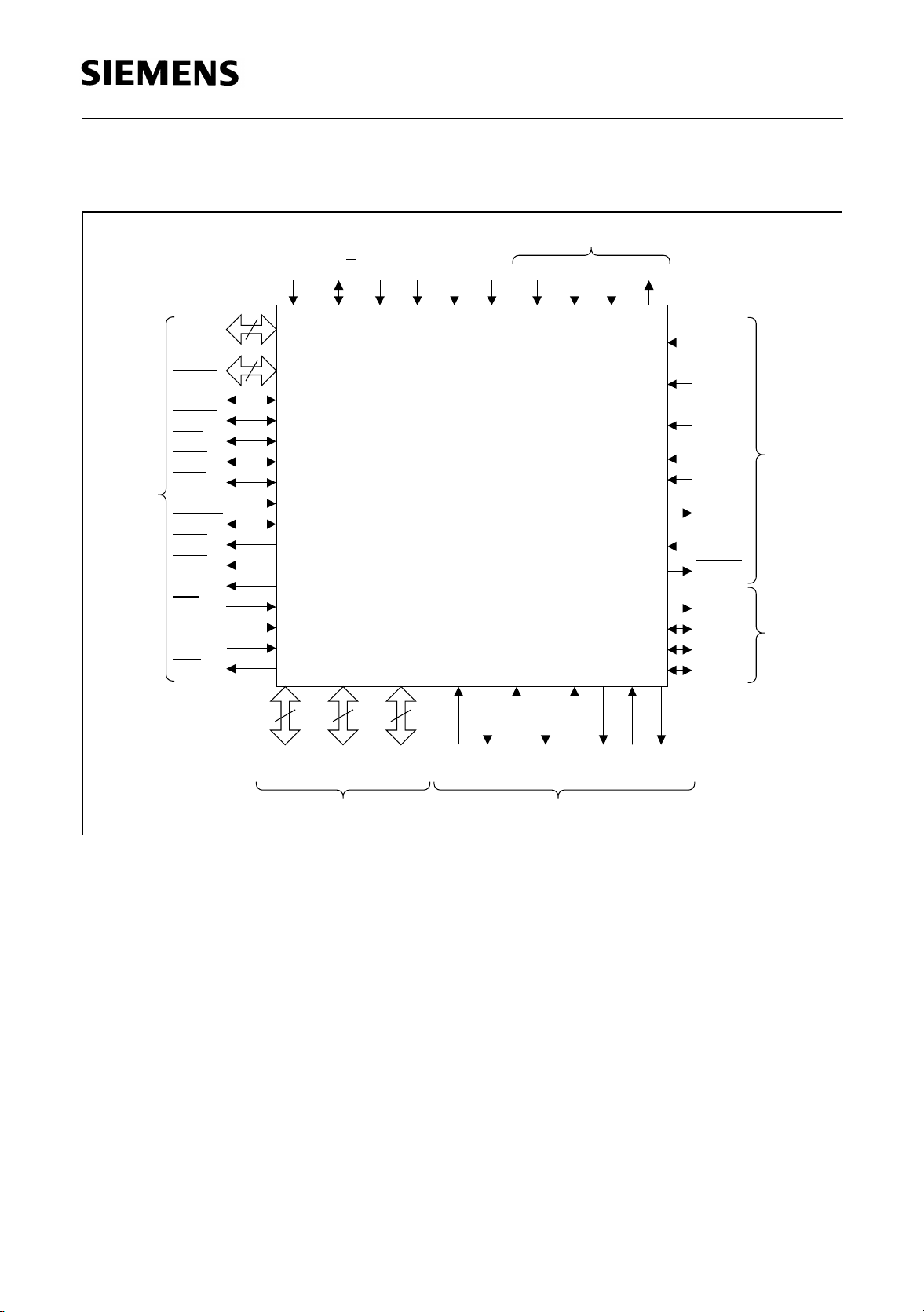
1.3 Pin Configuration
(top view)
SS
LD10 / A26
LD11 / A27
LD12 / A28
DD3
LD13 / A29
LD14 / A30
LD15 / A31
V
TDI
V
TMS
TCK
RXD / DD
RXCLK / DCL
RSP / FSC
TDO
P-MQFP-160-1
TXDEN
DRDY
TXD / DU
TSP
TXCLK
GP15 / MCLK
DD3
GP12 / N.C.3
GP14 / MTSR
GP13 / MRST
V
SS
V
SSVSS
DD3
V
V
GP9 / MCS2
GP10 / MCS1
GP11 / MCS0
GP8 / MCS3
TEST
DEMUX
GP7 / DRQTA
GP6 / DRQRA
GP5 / DRQTB
PEB 20321
Introduction
GP4 / DRQRB
GP3 / DACKTA
LD9 / A25
LD8 / A24
V
DD3
V
SS
LD7 / A23
LD6 / A22
LD5 / A21
LD4 / A20
LD3 / A19
LD2 / A18
LD1 / A17
LD0 / A16
V
SS
V
DD3
V
SS
RST
CLK
GNT
REQ
AD31
AD30
AD29
AD28
V
DD3
V
SS
AD27
AD26
AD25
AD24
C / BE3
IDSEL
AD23
AD22
V
DD3
V
SS
AD21
AD20
AD19
AD18
AD17
120
121
130
140
150
160
110 100 90
81
80
GP2 / DACKTB
GP1 / DACKRA
GP0 / DACKRB
LCSI
LCSO
LALE
LINTO
LINTI1
LINTI2
LBHE
V
70
DD3
V
SS
LWR
LRD
LRDY
LHLDA
LHOLD
LBREQ
W / R
MUNICH32X
PEB 20321
60
RESERVED 2
LA0 / A0
V
DD3
V
SS
LA1 / A1
LA2 / A2
LA3 / A3
LA4 / A4
LA5 / A5
LA6 / A6
LA7 / A7
LA8 / A8
50
LA9 / A9
V
DD3
V
SS
LA10 / A10
LA11 / A11
LA12 / A12
LA13 / A13
LA14 / A14
41
1
10 20 30 40
LA15 / A15
AD16
C / BE2
SS
DD3
V
V
FRAME
IRDY
TRDY
STOP
DEVSEL
PERR
SERR
PAR
DD5
V
DD5
DD3
VSSV
V
AD15
AD14
C / BE1
AD12
AD13
AD11
AD9
AD10
DD3
V
SS
V
AD8
AD7
AD6
AD5
AD4
C / BE0
AD3
AD2
DD3
V
SS
AD1
V
AD0
INTA
ITP10338
RESERVED 1
Figure 1
Semiconductor Group 12 1998-08-01
N.C.17
LD9/A25
LD8/A24
V
DD3
V
LD7/A23
LD6/A22 140
LD5/A21
LD4/A20
LD3/A19
LD2/A18
LD1/A17
LD0/A16
V
V
DD3
V
RST 150
CLK
GNT
REQ
AD31
AD30
AD29
AD28
V
DD3
V
AD27 160
AD26
AD25
AD24
C/BE3
IDSEL
AD23
AD22
V
DD3
V
AD21 170
AD20
AD19
AD18
AD17
N.C.18
N.C.19 176
133N.C.16
SS
SS
SS
SS
SS
132
1
N.C.15
N.C.14
LD10/A26
130
LD11/A27
LD12/A28
LD13/A29
LD14/A30
DD3VSS
LD15/A31
TDI
V
10
TMS
TCK
120
P-TQFP-176-1
TDO
RXCLK/DCL
RSP/FSC
RXD/DD
DRDY
TXDEN
TXD/DU
MUNICH32x
PEB 20321
20
TSP
TXCLK
GP15/MCLK
110
SSVSS
DD3
GP14/MTSR
GP13/MRST
GP12/N.C.3
V
V
30
DD3
VSSV
GP11/MCS0
GP10/MCS1
GP9/MCS2
GP8/MCS3
TEST
100
DEMUX
GP7/DRQTA
GP6/DRQRA
GP5/DRQTB
40
GP4/DRQRB
GP3/DACKTA
N.C.1389N.C.12
90
88
80 LINTO
70 LHOLD
60 LA4/A4
50 LA12/A12
45 N.C.8
44
PEB 20321
Introduction
N.C.11
N.C.10
GP2/DACKTB
GP1/DACKRA
GP0/DACKRB
LCSI
LCSO
LALE
LINTI1
LINTI2
LBHE
V
DD3
V
SS
LWR
LRD
LRDY
LHLDA
LBREQ
W/R
RESERVED2
LA0/A0
V
DD3
V
SS
LA1/A1
LA2/A2
LA3/A3
LA5/A5
LA6/A6
LA7/A7
LA8/A8
LA9/A9
V
DD3
V
SS
LA10/A10
LA11/A11
LA13/A13
LA14/A14
LA15/A15
N.C.9
Index
Marking
N.C.5
N.C.4
AD16
C/BE2
SS
DD3
V
V
FRAME
IRDY
TRDY
STOP
PERR
DEVSEL
RESERVED1
PAR
SERR
DD5
V
DD5
V
DD3
V
SS
V
AD15
C/BE1
AD13
AD14
AD11
AD12
AD9
AD10
V
DD3
SS
V
AD8
AD7
C/BE0
AD6
AD5
AD4
AD3
AD2
V
DD3
SS
AD1
V
AD0
INTA
N.C.6
N.C.7
ITP10702
Figure 2
Semiconductor Group 13 1998-08-01

PEB 20321
Introduction
Signal Type Definition:
The following signal type definitions are mainly taken from the PCI Specification
Revision 2.1:
in
out
t/s, I/O
s/t/s
o/d
Input is a standard input-only signal.
Totem Pole Output is a standard active driver.
Tri-State or I/O is a bi-directional, tri-state input/output pin.
Sustained Tri-State is an active low tri-state signal owned and driven
by one and only one agent at a time. (For further information refer to
the PCI Specification Revision 2.1)
Open Drain allows multiple devices to share as a wire-OR. A pull-up
is required to sustain the inactive state until another agent drives it,
and must be provided by the central resource.
Semiconductor Group 14 1998-08-01

Table 1
PCI Bus Interface Pins
PEB 20321
Introduction
Pin No.
P-MQFP160-1
1, 28, 38,
140…143,
146…149,
152, 153,
156…160,
19…25,
30…35, 39
Pin No.
P-TQFP176-1
3, 30, 40,
154…158,
160…163,
166, 167,
170…174,
21…27,
32…37,
41
Symbol I/O Function
AD(31:0) t/s Address/Data Bus
A bus transaction consists of an address
phase followed by one or more data
phases.
When MUNICH32X is Master, AD(31:0) are
outputs in the address phase of a
transaction. During the data phases ,
AD(31:0) remain outputs for write
transactions, and become inputs for read
transactions.
When MUNICH32X is Slave, AD(31:0) are
inputs in the address phase of a
transaction. During the data phases ,
AD(31:0) remain inputs for write
transactions, and become outputs for read
transactions.
AD(31:0) are updated and sampled on the
rising edge of CLK.
150, 2, 18, 29164, 4, 20, 31C/BE
(3:0) t/s Command/Byte Enable
During the address phase of a transaction,
(3:0) define the bus command. During
C/BE
the data phase, C/BE
(3:0) are used as Byte
Enables. The Byte Enables are valid for the
entire data phase and determine which
byte lanes carry meaningful data. C/BE
applies to byte 0 (lsb) and C/BE
byte 3 (msb).
When MUNICH32X is Master, C/BE
are outputs. When MUNICH32X is Slave,
(3:0) are inputs.
C/BE
(3:0) are updated and sampled on the
C/BE
rising edge of CLK.
0
3 applies to
(3:0)
Semiconductor Group 15 1998-08-01

Table 1
PCI Bus Interface Pins (cont’d)
PEB 20321
Introduction
Pin No.
P-MQFP160-1
Pin No.
P-TQFP176-1
Symbol I/O Function
13 15 PAR t/s Parity
PAR is even parity across AD(31:0) and
C/BE
clock after the address phase. PAR has the
same timing as AD(31:0) but delayed by
one clock.
When MUNICH32X is Master, PAR is
output during address phase and write data
phases. When MUNICH32X is Slave, PAR
is output during read data phases.
Parity errors detected by the MUNICH32X
are indicated on PERR
PAR is updated and sampled on the rising
edge of CLK.
3 5 FRAME
s/t/s Frame
FRAME
an access. FRAME
bus transa ction is b eginning. While FR AME
is asserted, data transfers continue. When
FRAME
the final phase.
When MUNICH32X is Master, FRAME
an output.
When MUNICH32X is Slave, FRAME
input.
FRAME
rising edge of CLK.
(3:0). PAR is stable and valid one
output.
indicates the beginning and end of
is asserted to indicate a
is deasserted, the transaction is in
is
is an
is updated and sampled on the
Semiconductor Group 16 1998-08-01
Table 1
PCI Bus Interface Pins (con t’d)
PEB 20321
Introduction
Pin No.
P-MQFP160-1
Pin No.
P-TQFP176-1
Symbol I/O Function
68IRDYs/t/s Initiator Ready
IRDY
indicates the bus master’s ability to
complete the current data phase of the
transaction. It is used in conjunction with
TRDY
. A data phase is completed on any
clock where both IRDY
sampled asserted. During a write, IRDY
indicates that valid data is present on
AD(31:0). During a read, it indicates the
master is prepared to accept data. Wait
cycles are inserted until both IRDY
TRDY
are asser ted together.
When MUNICH32X is Master, IRDY
output.
When MUNICH32X is Slave, IRDY
input.
IRDY
is updated and sampled on the rising
edge of CLK.
and TRDY are
and
is an
is an
79TRDY
s/t/s Target Ready
TRDY
indicates a slave’s ability to complete
the current data phase of the transaction.
During a read, TRDY
indicates that valid
data is presen t on AD(3 1:0). Duri ng a write,
it indicates the target is prepared to accept
data.
When MUNICH32X is Master, TRDY
is an
input.
When MUNICH32X is Slave, TRDY
is an
output.
TRDY
is updated and sampled on the rising
edge of CLK.
Semiconductor Group 17 1998-08-01
Table 1
PCI Bus Interface Pins (cont’d)
PEB 20321
Introduction
Pin No.
P-MQFP160-1
Pin No.
P-TQFP176-1
Symbol I/O Function
911STOPs/t/s STOP
STOP
is used by a slave to request the
current master to stop the current bus
transaction.
When MUNICH32X is Master, STOP
input.
When MUNICH32X is Slave, STOP
output.
STOP
is updated and sampled on the rising
edge of CLK.
151 165 IDSEL I Initialization Device Select
When MUNICH32X is slave in a
transaction, if IDSEL is active in the
address phase and C/BE
(3:0) indicates an
I/O read or write, the MUNICH32X
assumes a read or write to a configuration
register. In response, the MUNICH32X
asserts DEVSEL
during the subsequent
CLK cycle.
IDSEL is sampled on the rising edge of
CLK.
is an
is an
8 10 DEVSEL
s/t/s Device Select
When activated by a slave, it indicates to
the current bus master that the slave has
decoded its address as the target of the
current transaction. If no bus slave
activates DEVSEL
within six bus CLK
cycles, the master should abort the
transaction.
When MUNICH32X is master, DEVSEL
input. If DEVSEL
is not activated within six
is
clock cycles after an address is output on
AD(31:0), the MUNICH32X aborts the
transaction and generates an INTA
When MUNICH32X is slave, DEVSEL
.
is
output.
Semiconductor Group 18 1998-08-01
Table 1
PCI Bus Interface Pins (cont’d)
PEB 20321
Introduction
Pin No.
P-MQFP160-1
Pin No.
P-TQFP176-1
Symbol I/O Function
11 13 PERR s/t/s Parity Error
When activated, indicates a parity error
over the AD(31:0) and C/BE
(compared to the PAR input). It has a delay
of two CLK cycles with respect to AD and
(3:0) (i.e., it is valid for the cycle
C/BE
immediately following the corresponding
PAR cycle).
PERR
is asserted relative to the rising edge
of CLK.
12 14 SERR
o/d System Error
The MUNICH32X asserts this signal to
indicate a fatal system error.
SERR
is activated on the rising edge of
CLK.
(3:0) signals
139 153 REQ
t/s Request
Used by the MUNICH32X to request control
of the PCI.
REQ
138 152 GNT
t/s Grant
This signal is asserted by the arbiter to
grant control of the PCI to the MUNICH32X
in response to a bus request via REQ
is asserted, the MUNICH32X will
GNT
begin a bus transaction only after the
current bus Master has deasserted the
FRAME
is sampled on the rising edge of CLK.
GNT
137 151 CLK I Clock
Provides timing for all PCI transactions.
Most PCI signals are sampled or output
relative to the rising edge of CLK. The
actual clock frequency is either equal to the
frequency of CLK, or CLK frequency
divided by 2. The maximum CLK frequency
is 33 MHz.
is activated on the rising edge of CLK.
. After
signal.
Semiconductor Group 19 1998-08-01
Table 1
PCI Bus Interface Pins (cont’d)
PEB 20321
Introduction
Pin No.
P-MQFP160-1
Pin No.
P-TQFP176-1
Symbol I/O Function
136 150 RST I Reset
An asynchronous active low RST
brings all PCI registers, sequencers and
signals into a consistent state. All PCI
output signals are driven to their benign
state.
During RESET all output and I/O pins are in
tristate condition with the following
exception:
TXDEN is active high during RESET.
40 42 INTA
O (oD) Interrupt Request
When an interrupt status is active and
unmasked, the MUNICH32X activates this
open-drain output. Examples of interrupt
sources are transmission/reception error,
completion of transmit or receive packets
etc. The MUNICH32X deactivates INTA
when the interrupt status is acknowledged
via an appropriate action (e.g., specific
register write) and no other unmasked
interrupt statuses are active.
INTA
asynchronous to the CLK.
signal
is activated/ deactivated
Note: PCI control signals always require pull-up resistors. For the system dependent
pull-up recommendation please refer to PCI Specification Revision 2.1
chapter 4.3.3.
.
Semiconductor Group 20 1998-08-01

Table 2
Dedicated Pins
PEB 20321
Introduction
Pin No.
P-MQFP160-1
Pin No.
P-TQFP176-1
Symbol I/O Function
86 96 DEMUX I PCI/De-multiplexed Mode Select
DEMUX = 0 indicates normal PCI operation.
DEMUX = 1 indicates that the MUNICH32X is
operated in De-multiplexed mode.
62 68 W/R
I/O Write/Read
This signal distinguishes write and read
operations in the De-multiplexed mode. It is
tristate when the MUNICH32X is in PCI mode.
A Pull-Up resistor to V
is recommended if
DD3
De-multiplexed mode is not used.
10 12 RES. 1 I/O Reserved.
A Pull-Up resistor to V
is recommended.
DD3
61 67 RES. 2 O Reserved.
is recommended.
DD3
5, 17, 27,
37, 47, 58,
69, 92, 94,
95, 113,
124, 133,
135, 145,
155
7, 19, 29,
39, 53,
64, 75,
102, 104,
105, 123,
138, 147,
149, 159,
V
SS
A Pull-Up resistor to V
– Ground (0 V)
All pins must have the same level.
169
4, 16, 26,
36, 48, 59,
70, 93, 96,
114, 123,
134, 144,
154
6, 18, 28,
38, 54,
65, 76,
103, 106,
124, 137,
148, 158,
V
DD3
– Supply Voltage 3.3 V ± 0.3 V
All pins must have the same level.
168
14, 15 16, 17 V
DD5
– Supply Voltage 5 V ± 0.25 V
All pins must have the same level.
87 97 TEST I Test Input
When set to V
the MUNICH32X works in test
DD3
mode.
It must be set to V
Semiconductor Group 21 1998-08-01
for normal working mode.
SS
Table 2
Dedicated Pins (cont’d)
PEB 20321
Introduction
Pin No.
P-MQFP160-1
Pin No.
P-TQFP176-1
Symbol I/O Function
JTAG Test Port for Boundary Scan according to IEEE 1149.1
110 120 TCK I JTAG Test Clock
A Pull-Up resistor to V
DD3
boundary scan unit is not used.
111 1 21 TMS I JTAG Test Mode Select
A Pull-Up resistor to V
DD3
boundary scan unit is not used.
112 1 22 TD I I JTAG Test Data Input
A Pull-Up resistor to V
DD3
boundary scan unit is not used.
109 1 19 TD O O JTAG Test Data Output
Table 3
Local Bus Interface (LBI) Pins
is recommended if
is recommended if
is recommended if
Pin No.
P-MQFP160-1
41 … 46,
49 … 57,
60
Pin No.
P-TQFP176-1
47 … 52,
55 … 63,
66
Symbol I/O Function
LA(15:0)/
I/O
LBI Address
These pins provide the 16 bit Address bus for
the Local Bus Interface.
A(15:0)
I/O
A Pull-Down resistor to V
recommended if LBI is not used.
DEMUX Address
These pins provide the 16 least significant
address lines for the De-multiplexed Interface,
when DEMUX = 1.
SS
is
Semiconductor Group 22 1998-08-01
Table 3
Local Bus Interface (LBI) Pins (cont’d)
PEB 20321
Introduction
Pin No.
P-MQFP160-1
115…122,
125…132
Pin No.
P-TQFP176-1
125…130,
135, 136,
Symbol I/O Function
LD (15:0)/
139…146
A(31:16)
64 70 LHOLD
I/O
LBI Data
These pins provide the 16 bit Data bus for the
Local Bus Interface.
I/O
A Pull-Down resistor to V
SS
is
recommended if LBI is not used.
DEMUX Address
These pins provide the 16 most significant
address lines for the De-multiplexed Interface,
when DEMUX = 1.
I LBI Hold Request
LHOLD
mode. LHOLD
= 1 is used for normal bus drive
= 0 requests LBI to enter hold
mode.
A Pull-Up resistor to V
is recommended
DD3
if LBI is not used.
63 69 LBREQ
65 71 LHLDA
O LBI Bus Request
Output LBREQ
LBREQ
= 1 after regaining bus.
= 0 to request bus then set
I/O LBI Hold Status
As an outpu t, LHLDA
= 0 confirms that the LBI
bus is in HOLD mode.
As an input , LHLDA
= 1 means that
MUNICH32X must remain in hold mode.
A Pull-Up resistor to V
DD3
if LBI is not used.
76 82 LCSO
O LBI Chip Select Output
Used to select LBI external peripheral
77 83 LCSI
I LBI Chip Select Input
Used to select MUNICH32X as LBI Slave.
A Pull-Up resistor to V
DD3
if LBI is not used.
75 81 LALE O LBI Address Latch Enable
A Pull-Down resistor to V
recommended if LBI is not used.
is recommended
is recommended
is
SS
Semiconductor Group 23 1998-08-01
Table 3
Local Bus Interface (LBI) Pins (cont’d)
PEB 20321
Introduction
Pin No.
P-MQFP160-1
Pin No.
P-TQFP176-1
Symbol I/O Function
67 73 LRD I/O LBI Read Strobe
A Pull-Up resistor to V
is recommended
DD3
if LBI is not used.
68 74 LWR
I/O LBI Write Strobe
A Pull-Up resistor to V
is recommended
DD3
if LBI is not used.
71 77 LBHE
I/O LBI Byte High Enable
A Pull-Up resistor to V
is recommended
DD3
if LBI is not used.
66 72 LRDY
I/O LBI Ready Strobe to Extend Cycles
A Pull-Up resistor to V
is recommended
DD3
if LBI is not used.
73 79 LINTI1 I LBI Interrupt Input from Peripheral1
In case of bit HE1 in register LCONF is set
(HSCX register decoding selected) this pin
must be connected to V
if unused.
DD3
In case of bit HE1 in register LCONF is
reset (ESCC2 register decoding selected)
this pin must be connected to V
SS
if
unused.
72 78 LINTI2 I LBI Interrupt Input from Peripheral2
In case of bit HE1 in register LCONF is set
(HSCX register decoding selected) this pin
must be connected to V
if unused.
DD3
In case of bit HE1 in register LCONF is
reset (ESCC2 register decoding selected)
this pin must be connected to V
SS
if
unused.
74 80 LINTO O LBI Interrupt Output to Local
Microcontroller
Semiconductor Group 24 1998-08-01
.
Table 4
LBI DMA Support/General Purpose Bus Pins
PEB 20321
Introduction
Pin No.
P-MQFP160-1
Pin No.
P-TQFP176-1
Symbol I/O Function
85 95 DRQTA/
GP7
84 94 DRQRA/
GP6
83 93 DRQTB/
GP5
82 92 DRQRB/
GP4
81 91 DACKTA
GP3
I
DMA Request for Transmit Channel A
I/O
On reset, pin is General Purpose Bus pin
I
DMA Request for Receive Channel A
I/O
On reset, pin is General Purpose Bus pin
I
DMA Request for Transmit Channel B
I/O
On reset, pin is General Purpose Bus pin
I
DMA Request for Receive Channel B
I/O
On reset, pin is General Purpose Bus pin
/
O
DMA Acknowledge for Transmit Channel A
I/O
On reset, pin is General Purpose Bus pin
/
O
80 86 DACKTB
GP2
79 85 DACKRA
GP1
78 84 DACKRB
GP0
/
/
DMA Acknowledge for Transmit Channel B
I/O
On reset, pin is General Purpose Bus pin
O
DMA Acknowledge for Receive Channel A
I/O
On reset, pin is General Purpose Bus pin
O
DMA Acknowledge for Receive Channel B
I/O
On reset, pin is General Purpose Bus pin
Note: If bit ‘LBI’ is set to ‘1’ in register CONF i.e. DMA support for LBI operation is
selected controll ed by pin numbers 7 8..85, all unu sed pins must be c onn ected in
accordance with the following recommendation:
DRQTA, DRQRA, DRQTB, DRQRB to V
DACKTA, DACKTB, DACKRA, DACKRB Pull-Up to V
SS
DD3
If bit ‘LBI’ is set to ‘0’ in register CONF (RESET value) pins 78..85 provide the
General Purpose Port (GPP) pins 0..7. In this case a Pull-Up resistor to V
DD3
is
recommended for unused pins.
Semiconductor Group 25 1998-08-01
PEB 20321
Introduction
Table 5
Synchronous Serial Control (SSC) Interface/General Purpose Bus Pins
Pin No.
P-MQFP160-1
Pin No.
P-TQFP176-1
Symbol I/O Function
100 110 MCLK/
GP15
99 109 MTSR/
GP14
98 108 MRST/
GP13
97 106 N.C.3/
GP12
91 101 MCS0
GP11
I/O
SSC Shift Clock Input/Output
I/O
On reset, pin is General Purpose Bus pin
I/O
SSC Master Transmit/Slave Receive
I/O
On reset, pin is General Purpose Bus pin
I/O
SSC Master Receive/Slave Transmit
I/O
On reset, pin is General Purpose Bus pin
I/O
Reserved when in SSC Mode
I/O
On reset, pin is General Purpose Bus pin
/
O
SSC Chip select 0
I/O
On reset, pin is General Purpose Bus pin
90 100 MCS1
GP10
89 99 MCS2
GP9
88 98 MCS3
GP8
Note: Pull-Up resistors to V
whether they are configured a s General Purpose Port (GPP) pins 8..15 (RESET
value) or as Synchronous Serial Control (SSC) interface vi a bit ‘SSC’ in register
CONF.
/
O
SSC Chip select 1
I/O
On reset, pin is General Purpose Bus pin
/
O
SSC Chip select 2
I/O
On reset, pin is General Purpose Bus pin
/
O
SSC Chip select 3
I/O
On reset, pin is General Purpose Bus pin
are recommended for unused pins independent of
DD3
Semiconductor Group 26 1998-08-01

Table 6
PCM/IOM
®
-2 Interface Pins
PEB 20321
Introduction
Pin No.
P-MQFP160-1
Pin No.
P-TQFP176-1
Symbol I/O Function
108 118 RXCLK/
DCL
107 117 RSP/
FSC
I
Receive Clock
Provides the data clock for RXD
T1/DS1 24-channel 1.544 MHz
24-channel 1.536 MHz
CEPT 32-channel 2.048 MHz
32-channel 4.096 MHz
Additional new PCM modes:
3.088 MHz, 6.176 MHz, 8.192 MHz
(refer to MODE1 register description)
®
I/O
IOM
I
Receive Synchronization Pulse
-2 Data Clock
This signal provides the reference for the receive
PCM frame synchronization. It marks the first bit
in the PCM frame.
®
I/O
IOM
-2 Frame Synchronization
106 116 RXD/
I R ece ive Da ta
Serial dat a is received at t his PCM input port . The
MUNICH32X supports the T1/DS1 24-channel
PCM format, the CEPT 32-channel PCM format
as well as a 32-channel PCM format with
4.096-Mbit/s bit rate.
®
DD
IOM
-2 Data Downstream
101 111 TXCLK I Transmit Clock
Provides the data clock for TXD (refer to
RXCLK).
102 112 TSP I Transmit Synchronization Pulse
This signal provides the reference for the
transmit frame synchronization. It marks the last
bit in the PCM frame.
103 113 TXD/
O Transmit Data
Serial data sent by this PCM output port is
push-pull for active bits in the PCM frame and
tristate for inactive bits.
®
DU
IOM
-2 Data Upstream
Semiconductor Group 27 1998-08-01
Table 6
PCM/IOM
®
-2 Interface Pins (cont’d)
PEB 20321
Introduction
Pin No.
P-MQFP160-1
Pin No.
P-TQFP176-1
Symbol I/O Function
104 114 TXDEN O Transmit Data Enable
Indicates tristate of TXD
105 115 DRDY I Data Ready
A Pull-Up resistor to V
not used.
1
2
43
44
45
46
87
88
89
90
131
132
133
134
175
176
N.C.4
N.C.5
N.C.6
N.C.7
N.C.8
N.C.9
N.C.10
N.C.11
N.C.12
N.C.13
N.C.14
N.C.15
N.C.16
N.C.17
N.C.18
N.C.19
Not connected pins
It is recommended not to connect these pins.
is recommended if
DD3
Note: As a general recommendatio n 10 K Ohm re sistors con nected to V
used as Pull-Ups and 10 K Ohm resistors conn ected to V
should be used as
SS
should be
DD3
Pull-Downs.
Semiconductor Group 28 1998-08-01
1.4 Logic Symbol
PEB 20321
Introduction
Test Interface
PCI
Interface
AD(31:0)
C /
BE(3:0)
PAR
FRAME
IRDY
TRDY
STOP
IDSEL
DEVSEL
PERR
SERR
REQ
GNT
CLK
RST
INTA
DEMUX W / R TEST
32
4
16
V
SS DD3VDD5
16 13
V
MUNICH32X
PEB 20321
TCLK TMS TDI TDO
RXCLK /
DCL
RSP /
FSC
RXD /
DD
TXCLK
TSP
TXD /
DU
DRDY
TXDEN
MCS(3:0)
MRST
MCLK
MTSR
PCM /
IQM-2
Interface
SSC
Interface
LBI_CtrlLD(15:0)
DRQTA DRQRA
DACKRADACKTA DACKRBDACKTB
DMA Support InterfaceLocal Bus Interface
DRQRBDRQTB
ITL10455
Figure 3
MUNICH32X Logic Symbol
Note: To reduce complexity, the De-multiplexed General Purpose Bus (refer to pin
definition table) is not shown here.
Semiconductor Group 29 1998-08-01
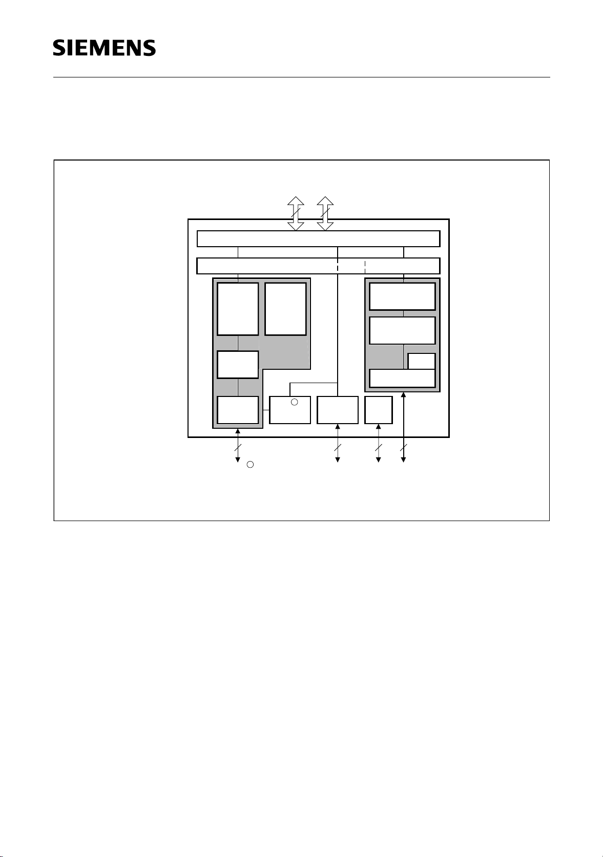
1.5 Functional Block Diagram The functional block diagrams are shown in Figure 4 and Figure 5.
PCI / Generic Bus
PEB 20321
Introduction
32 32
PCI System Bus Interface with FIFOs
DMA Controller 64 Channels 4 Channels
Config.
256 Byte
FIFOs
HDLC
Controller
PCM
Interface
PCM / IOM -2
R
Serial Data
Interface
and
State
Memory
Serial PCM
Core
R
IOM -2
Handle
SSC
Interface
8 4 8- / 16-Bit8
Serial
Port
Optional Generic Address BusMultiplexed PCI Address / Data Bus
JTAG
Test
Interface
Data
FIFOs
State
Machine
LBI
MBOX
LBI Interface
Local
Bus
ITB10339
Figure 4
Functional Block Overview of MUNICH32X
Semiconductor Group 30 1998-08-01
 Loading...