

Page 1

Siemens Mobile Phones
C55 Screenshots for Level 2.5e
Troubleshooting
V1.00
Version Date Department Notes to change
V 1.00 19.11.2002 ICM MP CCQ GRM New document
V 1.0 Page 1 of 8 ICM MP CCQ GRM
C55_Screenshots
Company Confidential
Copyright 2002© Siemens AG
11/02
Page 2

Table of Content
1 GENERAL INFORMATION 3
2 SPECIAL CIRCUIT DIAGRAM 3
3 SCREENSHOTS RX PATH 5
4 SCREENSHOTS TX PATH 5
5 SCREENSHOTS TX SIGNALS 6
6 SCREENSHOTS 26 MHZ VCO 6
7 SCREENSHOTS LO1 (RF VCO) 7
8 SCREENSHOTS LO2 (IF VCO) 7
9 SCREENSHOTS LOGIC VOLTAGES/SIGNALS 8
V 1.0 Page 2 of 8 ICM MP CCQ GRM
C55_Screenshots
Company Confidential
Copyright 2002© Siemens AG
11/02
Page 3
gr
Click shortcut to
open the document
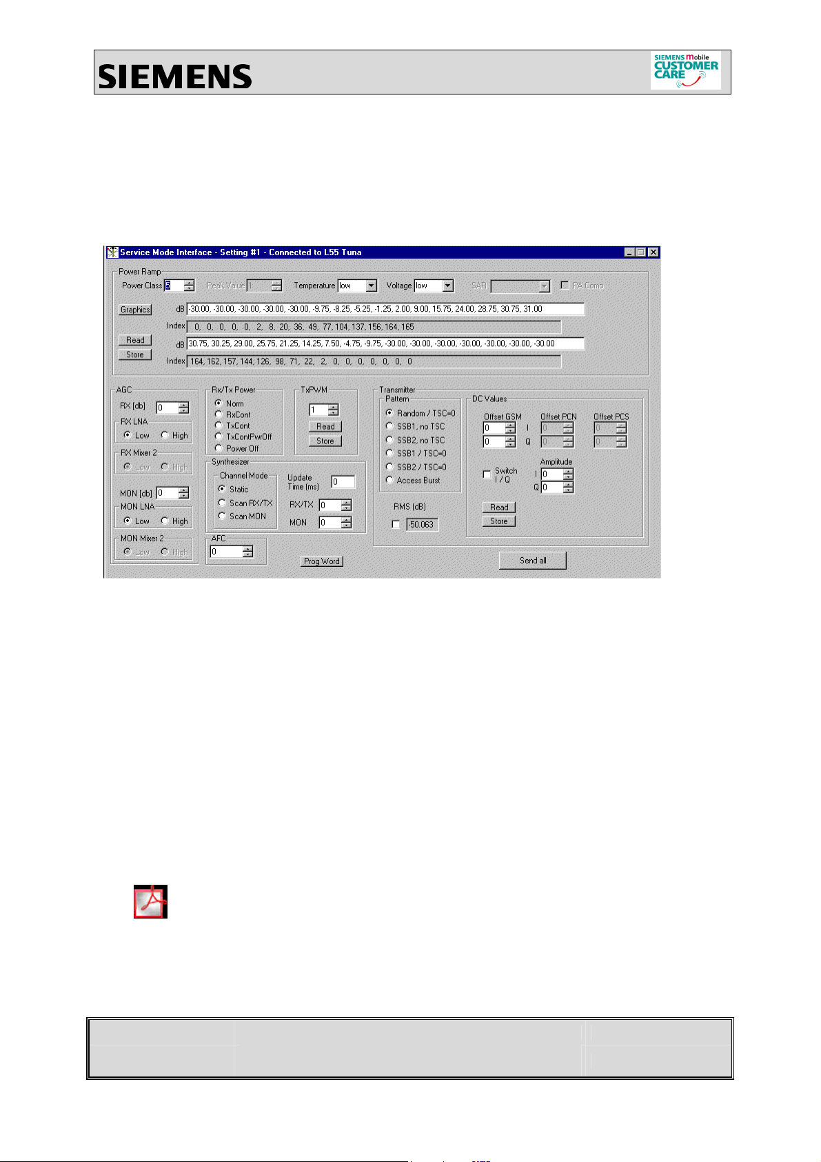
1 General Information
All measurements are done on channel 124 with WinSui Version 1.38. For all measurements an AFC
value is required. The LNA is active and the AGC is select to 20 dBm for RX measurements. Before
TX measurements the PCL, the TXPWM and the IQ Offset value must read out of the FLAH with the
READ buttons. For the Transmitter a random bit modulation with TSC 0 is used.
Abbreviations description:
Norm Rx/Tx Power – Normal Timing
RXCont Rx/Tx Power – RX Continues
TX Cont PA off Rx/Tx Power – TX Continues Power Amplifier off
RF GEN external RF Generator
Channel 124
Frequency Offset: 67.7 kHz
Level –50dBm
No BIT modulation
Continues Wave
2 Special Circuit Diagram
Special_Circuit_Dia
V 1.0 Page 3 of 8 ICM MP CCQ GRM
C55_Screenshots
am.pdf
Company Confidential
Copyright 2002© Siemens AG
11/02
Page 4

V 1.0 Page 4 of 8 ICM MP CCQ GRM
C55_Screenshots
Company Confidential
Copyright 2002© Siemens AG
11/02
Page 5

3 Screenshots RX Path
HF_OUT EGSM_RX RF_IQ
Z880_Pin1 Z880_Pin3/4 D800_Pin24/25/26/27
RX Cont RX Cont RX Cont
RF GEN RF GEN RF GEN
4 Screenshots TX Path
RF_IQ Vcont_TX VCO TXVCO_GSM_OUT
D800_Pin24/25/26/27 TP1620 D150_Pin7
Norm Norm Norm
RF GEN
TX_GSM_OUT HF_OUT
Z880_Pin14 Z880_Pin1
Norm Norm
(RF Probe with 1:10 divider) (RF Probe with 1:10 divider)
V 1.0 Page 5 of 8 ICM MP CCQ GRM
C55_Screenshots
Company Confidential
Copyright 2002© Siemens AG
11/02
Page 6

5 Screenshots TX Signals
PA_RAMP PCL5 Decoupled PA Signal PA_CTRL PCL5
R160 R932 R907
Norm Norm Norm
TXON1 TXONPA TXPWM
V921_Pin2 TP 1706 R931
Norm Norm Norm
6 Screenshots 26 MHz VCO
BB_SIN26M AFC_15000
TP 1501 R953
Norm Norm
V 1.0 Page 6 of 8 ICM MP CCQ GRM
C55_Screenshots
Company Confidential
Copyright 2002© Siemens AG
11/02
Page 7

7 Screenshots LO1 (RF VCO)
PLLON Vcont Mixer Out
V850_Pin2 TP 1610 C801
Norm Norm RX Cont
RF_VCO Out TX/RX RF_VCO Out RX RF_VCO Out TX
Z880_Pin1 Z880_Pin1 Z880_Pin1
TX Cont PA off/RX Cont RX Cont TX Cont PA off
8 Screenshots LO2 (IF VCO)
Vcont IF VCO IF_VCO
R831 C883
TX Cont PA off TX Cont PA off
V 1.0 Page 7 of 8 ICM MP CCQ GRM
C55_Screenshots
Company Confidential
Copyright 2002© Siemens AG
11/02
Page 8

9 Screenshots Logic Voltages/Signals
32 KHz Signal VCC_Syn/VCC2_8 WADOG
Z171 TP 1651/1650 TP 365
Norm Norm Norm
Vibra Signal Vibra UC GSM_ON
XG220_Pin2 V211_Pin3 D800_Pin23
Norm Norm Norm
V 1.0 Page 8 of 8 ICM MP CCQ GRM
C55_Screenshots
Company Confidential
Copyright 2002© Siemens AG
11/02
 Loading...