

Page 1
C515C
8-Bit CMOS Microcontroller
User's Manual 10.97
http://www.siemens.de/
Semiconductor/
Page 2

Edition 10.97
Published by Siemens AG,
Bereich Halbleiter, MarketingKommunikation, Balanstraße 73,
81541 München
©
Siemens AG 1997.
All Rights Reserved.
Attention please!
As far as patents or other rights of third parties are concerned, liability is only assumed for components, not for
applications, processes and circuits implemented within components or assemblies.
The information describes the type of component and shall not be considered as assured characteristics.
Terms of delivery and rights to change design reserved.
For questions on technology, delivery and prices please contact the Semiconductor Group Offices in Germany or
the Siemens Companies and Representatives worldwide (see address list).
Due to technical requirements components may contain dangerous substances. For information on the types in
question please contact your nearest Siemens Office, Semiconductor Group.
Siemens AG is an approved CECC manufacturer.
Packing
Please use the recycling operators known to you. We can also help you – get in touch with your nearest sales
office. By agreement we will take packing material back, if it is sorted. You must bear the costs of transport.
For packing material that is returned to us unsorted or which we are not obliged to accept, we shall have to invoice
you for any costs incurred.
Components used in life-support devices or systems must be expressly authorized for such purpose!
Critical components
systems
1 A critical component is a component used in a life-support device or system whose failure can reasonably be
2 Life support devices or systems are intended (a) to be implanted in the human body, or (b) to support and/or
2
with the express written approval of the Semiconductor Group of Siemens AG.
expected to cause the failure of that life-support device or system, or to affect its safety or effectiveness of that
device or system.
maintain and sustain human life. If they fail, it is reasonable to assume that the health of the user may be endangered.
1
of the Semiconductor Group of Siemens AG, may only be used in life-support devices or
Page 3

C515C User’s Manual
Revision History : 10.97
Previous Releases : 06.96 (Original Version)
General Information
C515C
Page (new
version)
general C515C-8E OTP version included (new chapter 10)
1-1
1-9
Table 1-1
2-2
3-2
3-3, 3-11,
4-4, 6-4,
Tab.3-2/3-3
Tab.3-2 /
3-3, pg.9-2
3-17
4-2, 4-5
4-3
4-10 - 4-12
4-11
4-12
6-6
6-10, 6-11
6-18
6-39, 6-43
6-57
6-72
6-105,
6-106
6-108
6-109
7-2
9-6, 9-7
9-7
9-8
9-15
Chapter 10
11-1
11-4 - 11-6
Page (prev.
version)
1-1
1-9
Table 1-1
2-2
3-2
3-3, 3-11,
4-4, 6-4,
Tab.3-2/3-3
Tab.3-2 /
3-3, pg.9-2
3-17
4-2, 4-5
4-3
4-10 - 4-12
4-11
4-12
6-6
6-10, 6-11
6-18
6-39, 6-43
6-57
6-72
6-105,
6-106
6-108
7-2
9-6, 9-7
9-7
9-8
9-15
10-1
10-3
Subjects (changes since last revision)
C515C AC/DC characteristics are now in chapter 11
Description of the new features of the C515C-8E; figure 1-1 modified
PSEN
Ports 1 to 5 and 7 descriptions are corrected to quasi-bidirectional
Figure 2-1 modified for C515C-8E
Section 3.1 : C515C-8E version included
Description of SYSCON : bit CSWO and C515C-8E reset value added
Description of PCON1 : bit WS and C515C-8E reset value added
Reset value of P4 and table entry for bit P7.0 (INT7) corrected;
Version registers for C515C-8E added
Figure 4-1 and 4-2 corrected
3rd paragraph of chapter 4.1.3 removed
Chapter 4.7 “ROM Protection...“ enhanced for OTP verification
Figure 4-5 corrected
Figure 4-5 : OTP version reference added
Figure 6-4 and text : delay part corrected
Figures 6-7 and 6-8 : delay part corrected
Figure 6-14 corrected
Figure 6-22 and 6-26 : figure content exchanged
6.4.3.: first paragraph, divider range corrected
Baudrate selection bits corrected
multiple formulas corrected
last paragraph added
Chapter 6.5.8 (CAN switch-off capability) added
Figure 7-1 : bit address for bit RXIE added
Adding P4.7/RXDC wake-up capability to the description
Figure 9-1 corrected
Additional text in last paragraph before 9.5
Note below figure 9-5 added
New chapter : describes OTP programming of the C515C-8E
Minimum value for ambient temperature under bias corrected to –40˚C
Improved and extended Icc specification
and ALE are activated every three (and not six) osc. periods
Semiconductor Group
Page 4

C515C User’s Manual
Revision History (cont’d) : 10.97
Previous Releases : 06.96 (Original Version)
General Information
C515C
Page (new
version)
11-10
11-11
11-14 to
11-17
Page (prev.
version)
10-8
10-10
-
Subjects (changes since last revision)
SSC timing parameter
(master mode) and
t
SCLK
improved
t
HI
Wrong figure “External Clock Cycle“ exchanged with correct figure
Programming interface characteristics added
Semiconductor Group
Page 5

General Information
C515C
Table of Contents Page
1 Introduction . . . . . . . . . . . . . . . . . . . . . . . . . . . . . . . . . . . . . . . . . . . . . . . . . . . . . . 1-1
1.1 Pin Configuration . . . . . . . . . . . . . . . . . . . . . . . . . . . . . . . . . . . . . . . . . . . . . . . . . . . 1-4
1.2 Pin Definitions and Functions. . . . . . . . . . . . . . . . . . . . . . . . . . . . . . . . . . . . . . . . . . 1-5
2 Fundamental Structure . . . . . . . . . . . . . . . . . . . . . . . . . . . . . . . . . . . . . . . . . . . . . 2-1
2.1 CPU . . . . . . . . . . . . . . . . . . . . . . . . . . . . . . . . . . . . . . . . . . . . . . . . . . . . . . . . . . . . . 2-3
2.2 CPU Timing . . . . . . . . . . . . . . . . . . . . . . . . . . . . . . . . . . . . . . . . . . . . . . . . . . . . . . . 2-5
3 Memory Organization . . . . . . . . . . . . . . . . . . . . . . . . . . . . . . . . . . . . . . . . . . . . . . 3-1
3.1 Program Memory, "Code Space" . . . . . . . . . . . . . . . . . . . . . . . . . . . . . . . . . . . . . . . 3-2
3.2 Data Memory, "Data Space". . . . . . . . . . . . . . . . . . . . . . . . . . . . . . . . . . . . . . . . . . . 3-2
3.3 General Purpose Registers . . . . . . . . . . . . . . . . . . . . . . . . . . . . . . . . . . . . . . . . . . . 3-2
3.4 XRAM Operation. . . . . . . . . . . . . . . . . . . . . . . . . . . . . . . . . . . . . . . . . . . . . . . . . . . . 3-3
3.4.1 XRAM/CAN Controller Access Control. . . . . . . . . . . . . . . . . . . . . . . . . . . . . . . . . . . 3-3
3.4.2 Accesses to XRAM using the DPTR (16-bit Addressing Mode). . . . . . . . . . . . . . . . 3-5
3.4.3 Accesses to XRAM using the Registers R0/R1 (8-bit Addressing Mode). . . . . . . . . 3-5
3.4.4 Reset Operation of the XRAM . . . . . . . . . . . . . . . . . . . . . . . . . . . . . . . . . . . . . . . . . 3-9
3.4.5 Behaviour of Port0 and Port2 . . . . . . . . . . . . . . . . . . . . . . . . . . . . . . . . . . . . . . . . . . 3-9
3.5 Special Function Registers. . . . . . . . . . . . . . . . . . . . . . . . . . . . . . . . . . . . . . . . . . . 3-11
4 External Bus Interface . . . . . . . . . . . . . . . . . . . . . . . . . . . . . . . . . . . . . . . . . . . . . . 4-1
4.1 Accessing External Memory. . . . . . . . . . . . . . . . . . . . . . . . . . . . . . . . . . . . . . . . . . . 4-1
4.1.1 Role of P0 and P2 as Data/Address Bus . . . . . . . . . . . . . . . . . . . . . . . . . . . . . . . . . 4-1
4.1.2 Timing. . . . . . . . . . . . . . . . . . . . . . . . . . . . . . . . . . . . . . . . . . . . . . . . . . . . . . . . . . . . 4-3
4.1.3 External Program Memory Access. . . . . . . . . . . . . . . . . . . . . . . . . . . . . . . . . . . . . . 4-3
4.2 PSEN
4.3 Overlapping External Data and Program Memory Spaces. . . . . . . . . . . . . . . . . . . . 4-3
4.4 ALE, Address Latch Enable . . . . . . . . . . . . . . . . . . . . . . . . . . . . . . . . . . . . . . . . . . . 4-4
4.5 Enhanced Hooks Emulation Concept. . . . . . . . . . . . . . . . . . . . . . . . . . . . . . . . . . . . 4-5
4.6 Eight Datapointers for Faster External Bus Access . . . . . . . . . . . . . . . . . . . . . . . . . 4-6
4.6.1 The Importance of Additional Datapointers . . . . . . . . . . . . . . . . . . . . . . . . . . . . . . . 4-6
4.6.2 How the eight Datapointers of the C515C are realized . . . . . . . . . . . . . . . . . . . . . . 4-6
4.6.3 Advantages of Multiple Datapointers . . . . . . . . . . . . . . . . . . . . . . . . . . . . . . . . . . . . 4-7
4.6.4 Application Example and Performance Analysis . . . . . . . . . . . . . . . . . . . . . . . . . . . 4-7
4.7 ROM/OTP Protection for the C515C-8R / C515C-8E . . . . . . . . . . . . . . . . . . . . . . 4-10
4.7.1 Unprotected ROM Mode. . . . . . . . . . . . . . . . . . . . . . . . . . . . . . . . . . . . . . . . . . . . . 4-10
4.7.2 Protected ROM/OTP Mode. . . . . . . . . . . . . . . . . . . . . . . . . . . . . . . . . . . . . . . . . . . 4-11
5 Reset and System Clock Operation . . . . . . . . . . . . . . . . . . . . . . . . . . . . . . . . . . . 5-1
5.1 Hardware Reset Operation. . . . . . . . . . . . . . . . . . . . . . . . . . . . . . . . . . . . . . . . . . . . 5-1
5.2 Hardware Reset Timing. . . . . . . . . . . . . . . . . . . . . . . . . . . . . . . . . . . . . . . . . . . . . . 5-3
5.3 Fast Internal Reset after Power-On . . . . . . . . . . . . . . . . . . . . . . . . . . . . . . . . . . . . . 5-4
5.4 Oscillator and Clock Circuit. . . . . . . . . . . . . . . . . . . . . . . . . . . . . . . . . . . . . . . . . . . . 5-6
5.5 System Clock Output . . . . . . . . . . . . . . . . . . . . . . . . . . . . . . . . . . . . . . . . . . . . . . . . 5-8
, Program Store Enable . . . . . . . . . . . . . . . . . . . . . . . . . . . . . . . . . . . . . . . . . 4-3
6 On-Chip Peripheral Components . . . . . . . . . . . . . . . . . . . . . . . . . . . . . . . . . . . . . 6-1
6.1 Parallel I/O . . . . . . . . . . . . . . . . . . . . . . . . . . . . . . . . . . . . . . . . . . . . . . . . . . . . . . . . 6-1
6.1.1 Port Structures . . . . . . . . . . . . . . . . . . . . . . . . . . . . . . . . . . . . . . . . . . . . . . . . . . . . . 6-1
Semiconductor Group I-1 1997-10-01
Page 6

General Information
C515C
Table of Contents Page
6.1.1.1 Port Structure Selection . . . . . . . . . . . . . . . . . . . . . . . . . . . . . . . . . . . . . . . . . . . . . . 6-3
6.1.1.2 Quasi-Bidirectional Port Structure . . . . . . . . . . . . . . . . . . . . . . . . . . . . . . . . . . . . . . 6-5
6.1.1.2.1 Basic Port Circuirty of Port 1 to 5 and 7 . . . . . . . . . . . . . . . . . . . . . . . . . . . . . . . . . . 6-5
6.1.1.2.2 Port 0 Circuitry . . . . . . . . . . . . . . . . . . . . . . . . . . . . . . . . . . . . . . . . . . . . . . . . . . . . . 6-8
6.1.1.2.3 Port 0 and Port 2 used as Address/Data Bus. . . . . . . . . . . . . . . . . . . . . . . . . . . . . . 6-9
6.1.1.2.4 SSC Port Pins of Port 4 . . . . . . . . . . . . . . . . . . . . . . . . . . . . . . . . . . . . . . . . . . . . . 6-10
6.1.1.3 Bidirectional (CMOS) Port Structure of Port 5 . . . . . . . . . . . . . . . . . . . . . . . . . . . . 6-12
6.1.1.3.1 Input Mode . . . . . . . . . . . . . . . . . . . . . . . . . . . . . . . . . . . . . . . . . . . . . . . . . . . . . . . 6-12
6.1.1.3.2 Output Mode. . . . . . . . . . . . . . . . . . . . . . . . . . . . . . . . . . . . . . . . . . . . . . . . . . . . . . 6-13
6.1.1.3.3 Hardware Power Down Mode. . . . . . . . . . . . . . . . . . . . . . . . . . . . . . . . . . . . . . . . . 6-15
6.1.2 Alternate Functions of Ports . . . . . . . . . . . . . . . . . . . . . . . . . . . . . . . . . . . . . . . . . . 6-16
6.1.3 Port Handling . . . . . . . . . . . . . . . . . . . . . . . . . . . . . . . . . . . . . . . . . . . . . . . . . . . . . 6-18
6.1.3.1 Port Timing . . . . . . . . . . . . . . . . . . . . . . . . . . . . . . . . . . . . . . . . . . . . . . . . . . . . . . . 6-18
6.1.3.2 Port Loading and Interfacing. . . . . . . . . . . . . . . . . . . . . . . . . . . . . . . . . . . . . . . . . . 6-19
6.1.3.3 Read-Modify-Write Feature of Ports 1 to 5 and 7. . . . . . . . . . . . . . . . . . . . . . . . . . 6-19
6.2 Timers/Counters. . . . . . . . . . . . . . . . . . . . . . . . . . . . . . . . . . . . . . . . . . . . . . . . . . . 6-21
6.2.1 Timer/Counter 0 and 1 . . . . . . . . . . . . . . . . . . . . . . . . . . . . . . . . . . . . . . . . . . . . . . 6-21
6.2.1.1 Timer/Counter 0 and 1 Registers . . . . . . . . . . . . . . . . . . . . . . . . . . . . . . . . . . . . . . 6-22
6.2.1.2 Mode 0 . . . . . . . . . . . . . . . . . . . . . . . . . . . . . . . . . . . . . . . . . . . . . . . . . . . . . . . . . . 6-25
6.2.1.3 Mode 1 . . . . . . . . . . . . . . . . . . . . . . . . . . . . . . . . . . . . . . . . . . . . . . . . . . . . . . . . . . 6-26
6.2.1.4 Mode 2 . . . . . . . . . . . . . . . . . . . . . . . . . . . . . . . . . . . . . . . . . . . . . . . . . . . . . . . . . . 6-27
6.2.1.5 Mode 3 . . . . . . . . . . . . . . . . . . . . . . . . . . . . . . . . . . . . . . . . . . . . . . . . . . . . . . . . . . 6-28
6.2.2 Timer/Counter 2 with Additional Compare/Capture/Reload . . . . . . . . . . . . . . . . . . 6-29
6.2.2.1 Timer 2 Registers . . . . . . . . . . . . . . . . . . . . . . . . . . . . . . . . . . . . . . . . . . . . . . . . . . 6-31
6.2.2.2 Timer 2 Operation. . . . . . . . . . . . . . . . . . . . . . . . . . . . . . . . . . . . . . . . . . . . . . . . . . 6-36
6.2.2.3 Compare Function of Registers CRC, CC1 to CC3 . . . . . . . . . . . . . . . . . . . . . . . . 6-38
6.2.2.3.1 Compare Mode 0 . . . . . . . . . . . . . . . . . . . . . . . . . . . . . . . . . . . . . . . . . . . . . . . . . . 6-38
6.2.2.3.2 Modulation Range in Compare Mode 0 . . . . . . . . . . . . . . . . . . . . . . . . . . . . . . . . . 6-40
6.2.2.3.3 Compare Mode 1 . . . . . . . . . . . . . . . . . . . . . . . . . . . . . . . . . . . . . . . . . . . . . . . . . . 6-42
6.2.2.4 Using Interrupts in Combination with the Compare Function . . . . . . . . . . . . . . . . . 6-44
6.2.2.5 Capture Function . . . . . . . . . . . . . . . . . . . . . . . . . . . . . . . . . . . . . . . . . . . . . . . . . . 6-46
6.3 Serial Interface . . . . . . . . . . . . . . . . . . . . . . . . . . . . . . . . . . . . . . . . . . . . . . . . . . . . 6-48
6.3.1 Multiprocessor Communication . . . . . . . . . . . . . . . . . . . . . . . . . . . . . . . . . . . . . . . 6-49
6.3.2 Serial Port Registers. . . . . . . . . . . . . . . . . . . . . . . . . . . . . . . . . . . . . . . . . . . . . . . . 6-49
6.3.3 Baud Rate Generation . . . . . . . . . . . . . . . . . . . . . . . . . . . . . . . . . . . . . . . . . . . . . . 6-51
6.3.3.1 Baud Rate in Mode 0 . . . . . . . . . . . . . . . . . . . . . . . . . . . . . . . . . . . . . . . . . . . . . . . 6-52
6.3.3.2 Baud Rate in Mode 2 . . . . . . . . . . . . . . . . . . . . . . . . . . . . . . . . . . . . . . . . . . . . . . . 6-52
6.3.3.3 Baud Rate in Mode 1 and 3 . . . . . . . . . . . . . . . . . . . . . . . . . . . . . . . . . . . . . . . . . . 6-53
6.3.3.3.1 Using the Internal Baud Rate Generator . . . . . . . . . . . . . . . . . . . . . . . . . . . . . . . . 6-53
6.3.3.3.2 Using Timer 1 to Generate Baud Rates . . . . . . . . . . . . . . . . . . . . . . . . . . . . . . . . . 6-55
6.3.4 Details about Mode 0 . . . . . . . . . . . . . . . . . . . . . . . . . . . . . . . . . . . . . . . . . . . . . . . 6-56
6.3.5 Details about Mode 1 . . . . . . . . . . . . . . . . . . . . . . . . . . . . . . . . . . . . . . . . . . . . . . . 6-59
6.3.6 Details about Modes 2 and 3 . . . . . . . . . . . . . . . . . . . . . . . . . . . . . . . . . . . . . . . . . 6-62
6.4 SSC Interface . . . . . . . . . . . . . . . . . . . . . . . . . . . . . . . . . . . . . . . . . . . . . . . . . . . . . 6-65
6.4.1 General Operation of the SSC . . . . . . . . . . . . . . . . . . . . . . . . . . . . . . . . . . . . . . . . 6-66
Semiconductor Group I-2 1997-10-01
Page 7

General Information
C515C
Table of Contents Page
6.4.2 Enable/Disable Control. . . . . . . . . . . . . . . . . . . . . . . . . . . . . . . . . . . . . . . . . . . . . . 6-66
6.4.3 Baudrate Generation (Master Mode only) . . . . . . . . . . . . . . . . . . . . . . . . . . . . . . . 6-67
6.4.4 Write Collision Detection. . . . . . . . . . . . . . . . . . . . . . . . . . . . . . . . . . . . . . . . . . . . . 6-67
6.4.5 Master/Slave Mode Selection. . . . . . . . . . . . . . . . . . . . . . . . . . . . . . . . . . . . . . . . . 6-68
6.4.6 Data/Clock Timing Relationships . . . . . . . . . . . . . . . . . . . . . . . . . . . . . . . . . . . . . . 6-69
6.4.6.1 Master Mode Operation . . . . . . . . . . . . . . . . . . . . . . . . . . . . . . . . . . . . . . . . . . . . . 6-69
6.4.6.2 Slave Mode Operation . . . . . . . . . . . . . . . . . . . . . . . . . . . . . . . . . . . . . . . . . . . . . . 6-70
6.4.7 Register Description . . . . . . . . . . . . . . . . . . . . . . . . . . . . . . . . . . . . . . . . . . . . . . . . 6-71
6.5 The On-Chip CAN Controller . . . . . . . . . . . . . . . . . . . . . . . . . . . . . . . . . . . . . . . . . 6-76
6.5.1 Basic CAN Controller Functions. . . . . . . . . . . . . . . . . . . . . . . . . . . . . . . . . . . . . . . 6-77
6.5.2 CAN Register Description. . . . . . . . . . . . . . . . . . . . . . . . . . . . . . . . . . . . . . . . . . . . 6-81
6.5.2.1 General Registers. . . . . . . . . . . . . . . . . . . . . . . . . . . . . . . . . . . . . . . . . . . . . . . . . . 6-81
6.5.2.2 The Message Object Registers / Data Bytes . . . . . . . . . . . . . . . . . . . . . . . . . . . . . 6-91
6.5.3 Handling of Message Objects. . . . . . . . . . . . . . . . . . . . . . . . . . . . . . . . . . . . . . . . . 6-97
6.5.4 Initialization and Reset . . . . . . . . . . . . . . . . . . . . . . . . . . . . . . . . . . . . . . . . . . . . . 6-104
6.5.5 Configuration of the Bit Timing . . . . . . . . . . . . . . . . . . . . . . . . . . . . . . . . . . . . . . . 6-105
6.5.5.1 Hard Synchronization and Resynchronization . . . . . . . . . . . . . . . . . . . . . . . . . . . 6-106
6.5.5.2 Calculation of the Bit Time . . . . . . . . . . . . . . . . . . . . . . . . . . . . . . . . . . . . . . . . . . 6-106
6.5.6 CAN Interrupt Handling. . . . . . . . . . . . . . . . . . . . . . . . . . . . . . . . . . . . . . . . . . . . . 6-107
6.5.7 CAN Controller in Power Saving Modes. . . . . . . . . . . . . . . . . . . . . . . . . . . . . . . . 6-108
6.5.8 Switch-off Capability of the CAN Controller (C515C-8E only) . . . . . . . . . . . . . . . 6-109
6.5.9 Configuration Examples of a Transmission Object. . . . . . . . . . . . . . . . . . . . . . . . 6-110
6.5.10 Configuration Examples of a Reception Object . . . . . . . . . . . . . . . . . . . . . . . . . . 6-111
6.5.11 The CAN Application Interface. . . . . . . . . . . . . . . . . . . . . . . . . . . . . . . . . . . . . . . 6-112
6.6 A/D Converter. . . . . . . . . . . . . . . . . . . . . . . . . . . . . . . . . . . . . . . . . . . . . . . . . . . . 6-113
6.6.1 A/D Converter Operation . . . . . . . . . . . . . . . . . . . . . . . . . . . . . . . . . . . . . . . . . . . 6-113
6.6.2 A/D Converter Registers. . . . . . . . . . . . . . . . . . . . . . . . . . . . . . . . . . . . . . . . . . . . 6-115
6.6.3 A/D Converter Clock Selection. . . . . . . . . . . . . . . . . . . . . . . . . . . . . . . . . . . . . . . 6-119
6.6.4 A/D Conversion Timing. . . . . . . . . . . . . . . . . . . . . . . . . . . . . . . . . . . . . . . . . . . . . 6-120
6.6.5 A/D Converter Calibration. . . . . . . . . . . . . . . . . . . . . . . . . . . . . . . . . . . . . . . . . . . 6-124
7 Interrupt System . . . . . . . . . . . . . . . . . . . . . . . . . . . . . . . . . . . . . . . . . . . . . . . . . . 7-1
7.1 Interrupt Registers . . . . . . . . . . . . . . . . . . . . . . . . . . . . . . . . . . . . . . . . . . . . . . . . . . 7-5
7.1.1 Interrupt Enable Registers . . . . . . . . . . . . . . . . . . . . . . . . . . . . . . . . . . . . . . . . . . . . 7-5
7.1.2 Interrupt Request / Control Flags. . . . . . . . . . . . . . . . . . . . . . . . . . . . . . . . . . . . . . . 7-8
7.1.3 Interrupt Priority Registers . . . . . . . . . . . . . . . . . . . . . . . . . . . . . . . . . . . . . . . . . . . 7-14
7.2 Interrupt Priority Level Structure. . . . . . . . . . . . . . . . . . . . . . . . . . . . . . . . . . . . . . . 7-15
7.3 How Interrupts are Handled . . . . . . . . . . . . . . . . . . . . . . . . . . . . . . . . . . . . . . . . . . 7-16
7.4 External Interrupts . . . . . . . . . . . . . . . . . . . . . . . . . . . . . . . . . . . . . . . . . . . . . . . . . 7-18
7.5 Interrupt Response Time . . . . . . . . . . . . . . . . . . . . . . . . . . . . . . . . . . . . . . . . . . . . 7-20
8 Fail Safe Mechanisms . . . . . . . . . . . . . . . . . . . . . . . . . . . . . . . . . . . . . . . . . . . . . . 8-1
8.1 Programmable Watchdog Timer. . . . . . . . . . . . . . . . . . . . . . . . . . . . . . . . . . . . . . . . 8-1
8.1.1 Input Clock Selection . . . . . . . . . . . . . . . . . . . . . . . . . . . . . . . . . . . . . . . . . . . . . . . . 8-2
8.1.2 Watchdog Timer Control / Status Flags. . . . . . . . . . . . . . . . . . . . . . . . . . . . . . . . . . 8-3
8.1.3 Starting the Watchdog Timer . . . . . . . . . . . . . . . . . . . . . . . . . . . . . . . . . . . . . . . . . . 8-4
Semiconductor Group I-3 1997-10-01
Page 8

General Information
C515C
Table of Contents Page
8.1.3.1 The First Possibility of Starting the Watchdog Timer . . . . . . . . . . . . . . . . . . . . . . . . 8-4
8.1.3.2 The Second Possibility of Starting the Watchdog Timer. . . . . . . . . . . . . . . . . . . . . . 8-4
8.1.4 Refreshing the Watchdog Timer. . . . . . . . . . . . . . . . . . . . . . . . . . . . . . . . . . . . . . . . 8-5
8.1.5 Watchdog Reset and Watchdog Status Flag . . . . . . . . . . . . . . . . . . . . . . . . . . . . . . 8-5
8.2 Oscillator Watchdog Unit . . . . . . . . . . . . . . . . . . . . . . . . . . . . . . . . . . . . . . . . . . . . . 8-6
9 Power Saving Modes . . . . . . . . . . . . . . . . . . . . . . . . . . . . . . . . . . . . . . . . . . . . . . . 9-1
9.1 Power Saving Mode Control Registers. . . . . . . . . . . . . . . . . . . . . . . . . . . . . . . . . . . 9-1
9.2 Idle Mode . . . . . . . . . . . . . . . . . . . . . . . . . . . . . . . . . . . . . . . . . . . . . . . . . . . . . . . . . 9-3
9.3 Slow Down Mode Operation. . . . . . . . . . . . . . . . . . . . . . . . . . . . . . . . . . . . . . . . . . . 9-5
9.4 Software Power Down Mode . . . . . . . . . . . . . . . . . . . . . . . . . . . . . . . . . . . . . . . . . . 9-6
9.4.1 Invoking Software Power Down Mode . . . . . . . . . . . . . . . . . . . . . . . . . . . . . . . . . . . 9-6
9.4.2 Exit from Software Power Down Mode. . . . . . . . . . . . . . . . . . . . . . . . . . . . . . . . . . . 9-7
9.5 State of Pins in Software Initiated Power Saving Modes . . . . . . . . . . . . . . . . . . . . . 9-8
9.6 Hardware Power Down Mode. . . . . . . . . . . . . . . . . . . . . . . . . . . . . . . . . . . . . . . . . . 9-9
9.7 Hardware Power Down Reset Timing. . . . . . . . . . . . . . . . . . . . . . . . . . . . . . . . . . . 9-11
9.8 CPUR Signal. . . . . . . . . . . . . . . . . . . . . . . . . . . . . . . . . . . . . . . . . . . . . . . . . . . . . . 9-15
10 OTP Memory Operation (C515C-8E only) . . . . . . . . . . . . . . . . . . . . . . . . . . . . . 10-1
10.1 Programming Configuration . . . . . . . . . . . . . . . . . . . . . . . . . . . . . . . . . . . . . . . . . . 10-1
10.2 Pin Configuration . . . . . . . . . . . . . . . . . . . . . . . . . . . . . . . . . . . . . . . . . . . . . . . . . . 10-2
10.3 Pin Definitions. . . . . . . . . . . . . . . . . . . . . . . . . . . . . . . . . . . . . . . . . . . . . . . . . . . . . 10-3
10.4 Programming Mode Selection . . . . . . . . . . . . . . . . . . . . . . . . . . . . . . . . . . . . . . . . 10-5
10.4.1 Basic Programming Mode Selection. . . . . . . . . . . . . . . . . . . . . . . . . . . . . . . . . . . . 10-5
10.4.2 OTP Memory Access Mode Selection . . . . . . . . . . . . . . . . . . . . . . . . . . . . . . . . . . 10-6
10.5 Program / Read OTP Memory Bytes . . . . . . . . . . . . . . . . . . . . . . . . . . . . . . . . . . . 10-7
10.6 Lock Bits Programming / Read. . . . . . . . . . . . . . . . . . . . . . . . . . . . . . . . . . . . . . . . 10-9
10.7 Access of Version Bytes. . . . . . . . . . . . . . . . . . . . . . . . . . . . . . . . . . . . . . . . . . . . 10-11
11 Device Specifications . . . . . . . . . . . . . . . . . . . . . . . . . . . . . . . . . . . . . . . . . . . . . 11-1
11.1 Absolute Maximum Ratings . . . . . . . . . . . . . . . . . . . . . . . . . . . . . . . . . . . . . . . . . . 11-1
11.2 DC Characteristics . . . . . . . . . . . . . . . . . . . . . . . . . . . . . . . . . . . . . . . . . . . . . . . . . 11-2
11.3 A/D Converter Characteristics . . . . . . . . . . . . . . . . . . . . . . . . . . . . . . . . . . . . . . . . 11-6
11.4 AC Characteristics for C515C. . . . . . . . . . . . . . . . . . . . . . . . . . . . . . . . . . . . . . . . . 11-8
11.5 OTP Memory Programming Mode Characteristics. . . . . . . . . . . . . . . . . . . . . . . . 11-14
11.6 ROM/OTP Verification Characteristics for C515C-8R / C515C-8E . . . . . . . . . . 11-18
11.7 Package Information. . . . . . . . . . . . . . . . . . . . . . . . . . . . . . . . . . . . . . . . . . . . . . . 11-21
12 Index . . . . . . . . . . . . . . . . . . . . . . . . . . . . . . . . . . . . . . . . . . . . . . . . . . . . . . . . . . . 12-1
Semiconductor Group I-4 1997-10-01
Page 9
Introduction
C515C
1 Introduction
The C515C is an enhanced, upgraded version of the SAB 80C515A 8-bit microcontroller which
additionally provides a full CAN interface, a SPI compatible synchronous serial interface, extended
power save provisions, additional on-chip RAM, 64K byte of on-chip program memory, two new
external interrupts and RFI related improvements. With a maximum external clock rate of 10 MHz
it achieves a 600 ns instruction cycle time (1
The C515C-8R contains a non-volatile 64k byte read-only program memory. The C515C-L is
identical to the C515C-8R, except that it lacks the on-chip program memory The C515C-8E is the
OTP version in the C515C microcontroller with a 64k byte one-time programmable (OTP) program
memory. With the C515C-8E fast programming cycles are achieved (1 byte in 100
several levels of OTP memory protection can be selected. If compared to the C515C-8R and
C515C-L, the C515C-8E OTP version additionally provides two features :
µ
s at 6 MHz).
µ
sec). Also
– the wake-up from software power down mode can, additionally to the external pin P3.2/INT0
wake-up capability, also be triggered alternatively by a second pin P4.7/RXDC.
– for power consumption reasons the on-chip CAN controller can be switched off
The term C515C refers to all versions within this documentation unless otherwise noted.
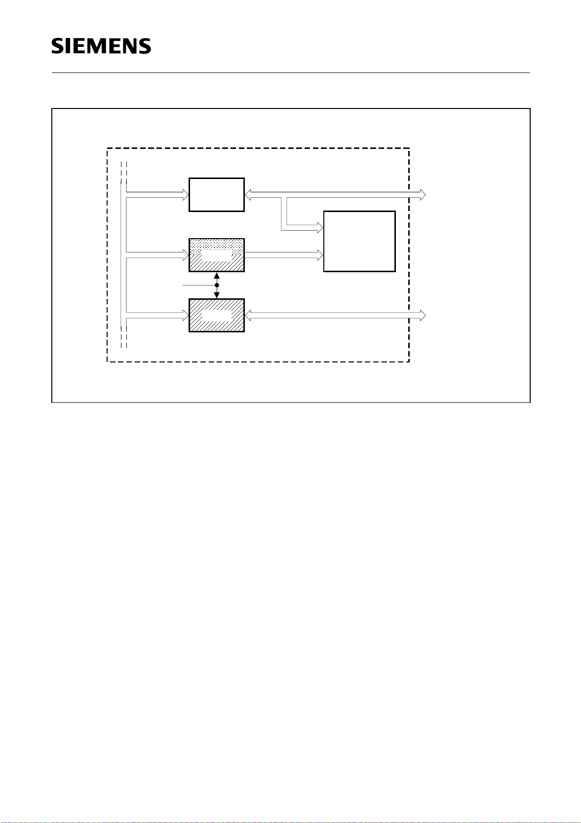
Figure 1-1 shows the different functional units of the C515C and figure 1-2 shows the simplified
logic symbol of the C515C.
SSC (SPI)
Interface
Oscillator
Watchdog
Power
Save Modes
Idle /
Power down
Slow down
On-Chip Emulation Support Module
Full-CAN
Controller
10-bit ADC
(8 inputs)
Timer 2
Capture/Compare
Unit
Port 4Port 5Port 6Port 7
XRAM
2K × 8
T0
CPU
8 Datapointer
T1
Program Memory
C515C-8R : 64k x 8 ROM
C515C-8E : 64k x 8 OTP
RAM
256 × 8
8-bit
USART
Port 0
Port 1
Port 2
Port 3
I/O
I/O
I/O
I/O
Analog /
I/O
Digital
Input
Figure 1-1
C515C Functional Units
Semiconductor Group 1-1 1997-10-01
I/O
I/O
Page 10

Listed below is a summary of the main features of the C515C:
•
Full upward compatibility with SAB 80C515A
•
On-chip program memory (with optional memory protection)
– C515C-8R : 64k byte on-chip ROM
– C515C-8E : 64k byte on-chip OTP
– alternatively up to 64k byte external program memory
•
64k byte on-chip ROM (external program execution is possible)
•
256 byte on-chip RAM
•
2K byte on-chip XRAM
•
Up to 64K byte external data memory
•
Superset of the 8051 architecture with 8 datapointers
•
Up to 10 MHz external operating frequency
– without clock prescaler (1
•
On-chip emulation support logic (Enhanced Hooks Technology
•
Current optimized oscillator circuit
•
Eight ports: 48 + 1 digital I/O lines, 8 analog inputs
– Quasi-bidirectional port structure (8051 compatible)
– Port 5 selectable for bidirectional port structure (CMOS voltage levels)
•
Three 16-bit timer/counters
– Timer 2 can be used for compare/capture functions
•
10-bit A/D converter with multiplexed inputs and Built-in self calibration
•
Full duplex serial interface with programmable baudrate generator (USART)
•
SSC synchronous serial interface (SPI compatible)
– Master and slave capable
– Programmable clock polarity / clock-edge to data phase relation
– LSB/MSB first selectable
– 1.25 MHz transfer rate at 10 MHz operating frequency
Full-CAN Module
•
– 256 register/data bytes are located in external data memory area
– max.1 MBaud at 10 MHz operating frequency
Seventeen interrupt vectors, at four priority levels selectable
•
Extended watchdog facilities
•
– 15-bit programmable watchdog timer
– Oscillator watchdog
Power saving modes
•
– Slow-down mode
– Idle mode (can be combined with slow-down mode)
– Software power-down mode with wake-up capability through INT0
– Hardware power-down mode
CPU running condition output pin
•
ALE can be switched off
•
Multiple separate VCC/VSS pin pairs
•
P-MQFP-80 package
•
Temperature Ranges: SAB-C515C
•
s instruction cycle time at 6 MHz external clock)
µ
TM
= 0 to 70 ° C
T
A
SAF-C515C
SAH-C515C
= - 40 to 85 ° C
T
A
= - 40 to 110 ° C
T
A
)
Introduction
or RXDC pin
C515C
Semiconductor Group 1-2 1997-10-01
Page 11
Introduction
C515C
Figure 1-2
Logic Symbol
Semiconductor Group 1-3 1997-10-01
Page 12
Introduction
1.1 Pin Configuration
This section describes the pin configuration of the C515C in the P-MQFP-80 package.
C515C
Figure 1-3
Pin Configuration (top view)
Semiconductor Group 1-4 1997-10-01
Page 13
1.2 Pin Definitions and Functions
This section describes all external signals of the C515C with its function.
Table 1-1
Pin Definitions and Functions
)
Symbol Pin Number I/O*
Function
P-MQFP-80
Introduction
C515C
P4.0-P4.7 72-74, 76-80
72
73
74
76
77
78
79
80
I/O Port 4
is an 8-bit quasi-bidirectional I/O port with internal pull-up
resistors. Port 4 pins that have 1’s written to them are
pulled high by the internal pull-up resistors, and in that
state can be used as inputs. As inputs, port 4 pins being
externally pulled low will source current (I
characteristics) because of the internal pull-up resistors.
P4 also contains the external A/D converter control pin,
the SSC pins, the CAN controller input/output lines, and
the external interrupt 8 input. The output latch
corresponding to a secondary function must be
programmed to a one (1) for that function to operate.
The alternate functions are assigned to port 4 as follows:
P4.0 ADST External A/D converter start pin
P4.1 SCLK SSC Master Clock Output /
P4.2 SRI SSC Receive Input
P4.3 STO SSC Transmit Output
P4.4 SLS Slave Select Input
P4.5 INT8 External interrupt 8 input
P4.6 TXDC Transmitter output of the CAN controller
P4.7 RXDC Receiver input of the CAN controller
SSC Slave Clock Input
, in the DC
IL
PE
/SWD 75 I Power saving mode enable / Start watchdog timer
A low level on this pin allows the software to enter the
power down, idle and slow down mode. In case the low
level is also seen during reset, the watchdog timer
function is off on default.
Use of the software controlled power saving modes is
blocked, when this pin is held on high level. A high level
during reset performs an automatic start of the watchdog
timer immediately after reset. When left unconnected this
pin is pulled high by a weak internal pull-up resistor.
RESET
1IRESET
A low level on this pin for the duration of two machine
cycles while the oscillator is running resets the C515C. A
small internal pullup resistor permits power-on reset
using only a capacitor connected to VSS.
*) I = Input
O = Output
Semiconductor Group 1-5 1997-10-01
Page 14

Table 1-1
Pin Definitions and Functions (cont’d)
Symbol Pin Number I/O*)Function
P-MQFP-80
VAREF 3 – Reference voltage for the A/D converter
VAGND 4 – Reference ground for the A/D converter
P6.7-P6.0 5-12 I Port 6
is an 8-bit unidirectional input port to the A/D converter.
Port pins can be used for digital input, if voltage levels
simultaneously meet the specifications high/low input
voltages and for the eight multiplexed analog inputs.
Introduction
C515C
P3.0-P3.7 15-22
15
16
17
18
19
20
21
22
I/O Port 3
is an 8-bit quasi-bidirectional I/O port with internal pullup
resistors. Port 3 pins that have 1's written to them are
pulled high by the internal pullup resistors, and in that
state can be used as inputs. As inputs, port 3 pins being
externally pulled low will source current (I
characteristics) because of the internal pullup resistors.
Port 3 also contains the interrupt, timer, serial port and
external memory strobe pins that are used by various
options. The output latch corresponding to a secondary
function must be programmed to a one (1) for that
function to operate. The secondary functions are
assigned to the pins of port 3, as follows:
P3.0 RXD Receiver data input (asynch.) or
P3.1 TXD Transmitter data output (asynch.) or
P3.2 INT0
P3.3 INT1 External interrupt 1 input / timer 1
P3.4 T0 Timer 0 counter input
P3.5 T1 Timer 1 counter input
P3.6 WR WR control output; latches the data
P3.7 RD RD control output; enables the
, in the DC
IL
data input/output (synch.) of serial
interface
clock output (synch.) of serial
interface
External interrupt 0 input / timer 0
gate control input
gate control input
byte from port 0 into the external
data memory
external data memory
*) I = Input
O = Output
Semiconductor Group 1-6 1997-10-01
Page 15

Table 1-1
Pin Definitions and Functions (cont’d)
Symbol Pin Number I/O*)Function
P-MQFP-80
P7.0 23 I/O Port 7
is an 1-bit quasi-bidirectional I/O port with internal pull-up
resistor. When a 1 is written to P7.0 it is pulled high by an
internal pull-up resistor, and in that state can be used as
input. As input, P7.0 being externally pulled low will
source current (I IL, in the DC characteristics) because of
the internal pull-up resistor. If P7.0 is used as interrupt
input, its output latch must be programmed to a one (1).
The secondary function is assigned to the port 7 pin as
follows:
P7.0 INT7 Interrupt 7 input
Introduction
C515C
P1.0 - P1.7 31-24
31
30
29
28
27
26
25
24
I/O Port 1
is an 8-bit quasi-bidirectional I/O port with internal pullup
resistors. Port 1 pins that have 1's written to them are
pulled high by the internal pullup resistors, and in that
state can be used as inputs. As inputs, port 1 pins being
externally pulled low will source current (I
characteristics) because of the internal pullup resistors.
The port is used for the low-order address byte during
program verification. Port 1 also contains the interrupt,
timer, clock, capture and compare pins that are used by
various options. The output latch corresponding to a
secondary function must be programmed to a one (1) for
that function to operate (except when used for the
compare functions). The secondary functions are
assigned to the port 1 pins as follows:
P1.0 INT3
P1.1 INT4 CC1 Interrupt 4 input / compare 1 output /
P1.2 INT5 CC2 Interrupt 5 input / compare 2 output /
P1.3 INT6 CC3 Interrupt 6 input / compare 3 output /
P1.4 INT2 Interrupt 2 input
P1.5 T2EX Timer 2 external reload / trigger
P1.6 CLKOUT System clock output
P1.7 T2 Counter 2 input
, in the DC
IL
CC0 Interrupt 3 input / compare 0 output /
capture 0 input
capture 1 input
capture 2 input
capture 3 input
input
*) I = Input
O = Output
Semiconductor Group 1-7 1997-10-01
Page 16

Table 1-1
Pin Definitions and Functions (cont’d)
Symbol Pin Number I/O*)Function
P-MQFP-80
XTAL2 36 – XTAL2
Input to the inverting oscillator amplifier and input to the
internal clock generator circuits.
To drive the device from an external clock source, XTAL2
should be driven, while XTAL1 is left unconnected.
Minimum and maximum high and low times as well as
rise/fall times specified in the AC characteristics must be
observed.
XTAL1 37 – XTAL1
Output of the inverting oscillator amplifier.
Introduction
C515C
P2.0-P2.7 38-45 I/O Port 2
is an 8-bit quasi-bidirectional I/O port with internal pullup
resistors. Port 2 pins that have 1's written to them are
pulled high by the internal pullup resistors, and in that
state can be used as inputs. As inputs, port 2 pins being
externally pulled low will source current (I
characteristics) because of the internal pullup resistors.
Port 2 emits the high-order address byte during fetches
from external program memory and during accesses to
external data memory that use 16-bit addresses
(MOVX @DPTR). In this application it uses strong
internal pullup resistors when issuing 1's. During
accesses to external data memory that use 8-bit
addresses (MOVX @Ri), port 2 issues the contents of
the P2 special function register.
CPUR
46 O CPU running condition
This output pin is at low level when the CPU is running
and program fetches or data accesses in the external
data memory area are executed. In idle mode, hardware
and software power down mode, and with an active
RESET signal CPUR is set to high level.
CPUR can be typically used for switching external
memory devices into power saving modes.
, in the DC
IL
*) I = Input
O = Output
Semiconductor Group 1-8 1997-10-01
Page 17

Table 1-1
Pin Definitions and Functions (cont’d)
Symbol Pin Number I/O*)Function
P-MQFP-80
PSEN 47 O The Program Store Enable
output is a control signal that enables the external
program memory to the bus during external fetch
operations. It is activated every three oscillator periods,
except during external data memory accesses. The
signal remains high during internal program execution.
ALE 48 O The Address Latch enable
output is used for latching the address into external
memory during normal operation. It is activated every
three oscillator periods, except during an external data
memory access. ALE can be switched off when the
program is executed internally.
Introduction
C515C
EA 49 I External Access Enable
When held high, the C515C executes instructions always
from internal program memory. When EA is held low, all
instructions are fetched from external program memory.
EA should not be driven during reset operation
P0.0-P0.7 52-59 I/O Port 0
is an 8-bit open-drain bidirectional I/O port.
Port 0 pins that have 1's written to them float, and in that
state can be used as high-impedance inputs.
Port 0 is also the multiplexed low-order address and data
bus during accesses to external program and data
memory. In this application it uses strong internal pullup
resistors when issuing 1's. Port 0 also outputs the code
bytes during program verification in the C515C-8E.
External pullup resistors are required during program.
P5.7-P5.0 60-67 I/O Port 5
is an 8-bit quasi-bidirectional I/O port with internal pullup
resistors. Port 5 pins that have 1's written to them are
pulled high by the internal pullup resistors, and in that
state can be used as inputs. As inputs, port 5 pins being
externally pulled low will source current (I
characteristics) because of the internal pullup resistors.
Port 5 can also be switched into a bidirectional mode, in
which CMOS levels are provided. In this bidirectional
mode, each port 5 pin can be programmed individually as
input or output.
, in the DC
IL
*) I = Input
O = Output
Semiconductor Group 1-9 1997-10-01
Page 18
Table 1-1
Pin Definitions and Functions (cont’d)
Symbol Pin Number I/O*)Function
P-MQFP-80
Introduction
C515C
HWPD
VCC1 33 – Supply voltage for internal logic
VSS1 34 – Ground (0 V) for internal logic
VCCE1
VCCE2
VSSE1
VSSE2
VCCEXT 50 – Supply voltage for external access pins
69 I Hardware Power Down
A low level on this pin for the duration of one machine
cycle while the oscillator is running resets the C515C.
A low level for a longer period will force the part to power
down mode with the pins floating.
This pins is used for the power supply of the internal logic
circuits during normal, idle, and power down mode.
This pin is used for the ground connection of the internal
logic circuits during normal, idle, and power down mode.
32
68
35
70
– Supply voltage for I/O ports
These pins are used for power supply of the I/O ports
during normal, idle, and power-down mode.
– Ground (0 V) for I/O ports
These pins are used for ground connections of the I/O
ports during normal, idle, and power-down mode.
This pin is used for power supply of the I/O ports and
control signals which are used during external accesses
(for Port 0, Port 2, ALE, PSEN
, P3.6/WR, and P3.7/RD).
VSSEXT 51 – Ground (0 V) for external access pins
This pin is used for the ground connection of the I/O ports
and control signals which are used during external
accesses (for Port 0, Port 2, ALE, PSEN
P3.7/RD).
VCCCLK 14 – Supply voltage for on-chip oscillator
This pin is used for power supply of the on-chip oscillator
circuit.
VSSCLK 13 – Ground (0 V) for on-chip oscillator
This pin is used for ground connection of the on-chip
oscillator circuit.
N.C. 2, 71 – Not connected
These pins should not be connected.
*) I = Input
O = Output
Semiconductor Group 1-10 1997-10-01
, P3.6/WR, and
Page 19

Fundamental Structure
C515C
2 Fundamental Structure
The C515C is fully compatible to the architecture of the standard 8051/C501 microcontroller family.
While maintaining all architectural and operational characteristics of the C501, the C515C
incorporates a CPU with 8 datapointers, a genuine 10-bit A/D converter, a capture/compare unit, a
Full-CAN controller unit, a SSC synchronous serial interface, a USART serial interface, a XRAM
data memory as well as some enhancements in the Fail Save Mechanism Unit. Figure 2-1 shows
a block diagram of the C515C.
Semiconductor Group 2-1 1997-10-01
Page 20
C515C
Fundamental Structure
C515C
XTAL1
XTAL2
ALE
PSEN
EA
CPUR
PE/SWD
HWPD
RESET
Oscillator Watchdog
OSC & Timing
CPU
8 Datapointers
Programmable
Watchdog Timer
Timer 0
Timer 1
Timer 2
Capture/Compare
Unit
XRAM
2k x 8
RAM
256 x 8
ROM/
OTP
64k x 8
Emulation
Support
Logic
Port 0
Port 1
Port 2
multiple
Vcc/Vss
Lines
Port 0
8-bit digit. I/O
Port 1
8-bit digit. I/O
Port 2
8-bit digit. I/O
USART
Baud Rate Generator
SSC (SPI) Interface
Full-CAN
Controller
Interrupt Unit
V
V
AGND
AREF
A/D Converter
10-Bit
S&H
MUX
Figure 2-1
Block Diagram of the C515C
256 Byte
Reg./Data
Port 3
Port 4
Port 5
Port 7
Port 6
Port 3
8-bit digit. I/O
Port 4
8-bit digit. I/O
Port 5
8-bit digit. I/O
Port 7
1-bit digit. I/O
Port 6
8-bit analog /
digital Input
Semiconductor Group 2-2 1997-10-01
Page 21

Fundamental Structure
C515C
2.1 CPU
The C515C is efficient both as a controller and as an arithmetic processor. It has extensive facilities
for binary and BCD arithmetic and excels in its bit-handling capabilities. Efficient use of program
memory results from an instruction set consisting of 44% one-byte, 41% two-byte, and 15% threebyte instructions. With a 6 MHz external clock, 58% of the instructions execute in 1.0 µs (10 MHz:
600 ns).
The CPU (Central Processing Unit) of the C515C consists of the instruction decoder, the arithmetic
section and the program control section. Each program instruction is decoded by the instruction
decoder. This unit generates the internal signals controlling the functions of the individual units
within the CPU. They have an effect on the source and destination of data transfers and control the
ALU processing.
The arithmetic section of the processor performs extensive data manipulation and is comprised of
the arithmetic/logic unit (ALU), an A register, B register and PSW register.
The ALU accepts 8-bit data words from one or two sources and generates an 8-bit result under the
control of the instruction decoder. The ALU performs the arithmetic operations add, substract,
multiply, divide, increment, decrement, BDC-decimal-add-adjust and compare, and the logic
operations AND, OR, Exclusive OR, complement and rotate (right, left or swap nibble (left four)).
Also included is a Boolean processor performing the bit operations as set, clear, complement, jumpif-not-set, jump-if-set-and-clear and move to/from carry. Between any addressable bit (or its
complement) and the carry flag, it can perform the bit operations of logical AND or logical OR with
the result returned to the carry flag.
The program control section controls the sequence in which the instructions stored in program
memory are executed. The 16-bit program counter (PC) holds the address of the next instruction to
be executed. The conditional branch logic enables internal and external events to the processor to
cause a change in the program execution sequence.
Additionally to the CPU functionality of the C501/8051 standard microcontroller, the C515C
contains 8 datapointers. For complex applications with peripherals located in the external data
memory space (e.g. CAN controller) or extended data storage capacity this turned out to be a "bottle
neck" for the 8051’s communication to the external world. Especially programming in high-level
languages (PLM51, C51, PASCAL51) requires extended RAM capacity and at the same time a fast
access to this additional RAM because of the reduced code efficiency of these languages.
Accumulator
ACC is the symbol for the accumulator register. The mnemonics for accumulator-specific
instructions, however, refer to the accumulator simply as A.
Program Status Word
The Program Status Word (PSW) contains several status bits that reflect the current state of the
CPU.
Semiconductor Group 2-3 1997-10-01
Page 22
Fundamental Structure
C515C
Special Function Register PSW (Address D0H) Reset Value : 00H
Bit No. MSB LSB
H
D7
CY AC
H
D6
H
D5
F0
H
D4
RS1 RS0 OV F1 PD0
Bit Function
CY Carry Flag
Used by arithmetic instruction.
AC Auxiliary Carry Flag
Used by instructions which execute BCD operations.
F0 General Purpose Flag
RS1
RS0
Register Bank select control bits
These bits are used to select one of the four register banks.
RS1 RS0 Function
0 0 Bank 0 selected, data address 00H-07
0 1 Bank 1 selected, data address 08H-0F
1 0 Bank 2 selected, data address 10H-17
1 1 Bank 3 selected, data address 18H-1F
H
D3
H
D2
H
D1
H
D0
H
PSW
H
H
H
H
OV Overflow Flag
Used by arithmetic instruction.
F1 General Purpose Flag
P Parity Flag
Set/cleared by hardware after each instruction to indicate an odd/even
number of "one" bits in the accumulator, i.e. even parity.
B Register
The B register is used during multiply and divide and serves as both source and destination. For
other instructions it can be treated as another scratch pad register.
Stack Pointer
The stack pointer (SP) register is 8 bits wide. It is incremented before data is stored during PUSH
and CALL executions and decremented after data is popped during a POP and RET (RETI)
execution, i.e. it always points to the last valid stack byte. While the stack may reside anywhere in
the on-chip RAM, the stack pointer is initialized to 07H after a reset. This causes the stack to begin
a location = 08H above register bank zero. The SP can be read or written under software control.
Semiconductor Group 2-4 1997-10-01
Page 23

Fundamental Structure
C515C
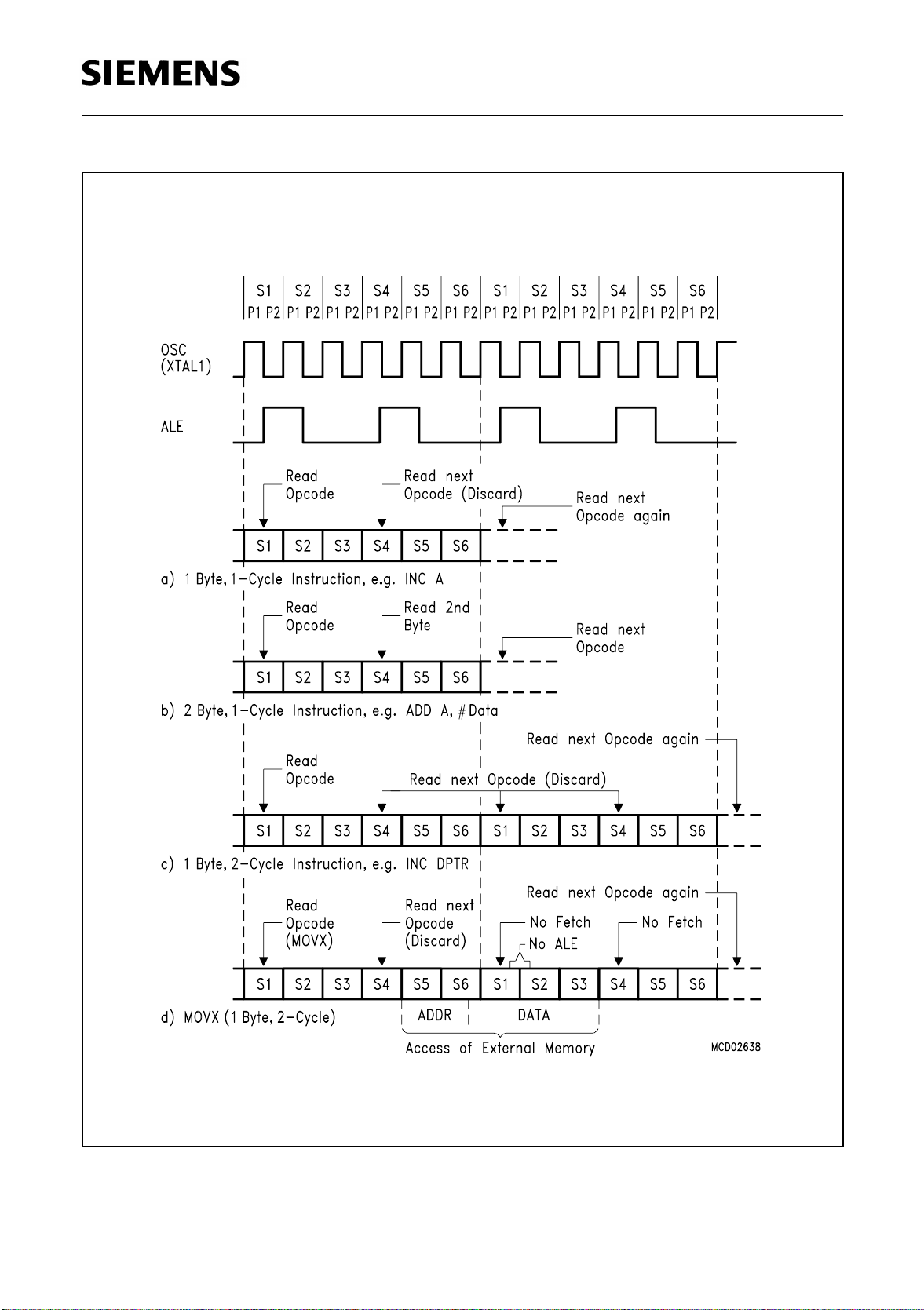
2.2 CPU Timing
The C515C has no clock prescaler. Therefore, a machine cycle of the C515C consists of 6 states
(6 oscillator periods). Each state is divided into a phase 1 half and a phase 2 half. Thus, a machine
cycle consists of 6 oscillator periods, numbered S1P1 (state 1, phase 1) through S6P2 (state 6,
phase 2). Each state lasts one oscillator period. Typically, arithmetic and logic operations take place
during phase 1 and internal register-to-register transfers take place during phase 2.
The diagrams in figure 2-2 show the fetch/execute timing related to the internal states and phases.
Since these internal clock signals are not user-accessible, the XTAL1 oscillator signals and the ALE
(address latch enable) signal are shown for external reference. ALE is normally activated twice
during each machine cycle: once during S1P2 and S2P1, and again during S4P2 and S5P1.
Executing of a one-cycle instruction begins at S1P2, when the op-code is latched into the instruction
register. If it is a two-byte instruction, the second reading takes place during S4 of the same
machine cycle. If it is a one-byte instruction, there is still a fetch at S4, but the byte read (which would
be the next op-code) is ignored (discarded fetch), and the program counter is not incremented. In
any case, execution is completed at the end of S6P2.
Figures 2-2 (a) and (b) show the timing of a 1-byte, 1-cycle instruction and for a 2-byte, 1-cycle
instruction.
Semiconductor Group 2-5 1997-10-01
Page 24
Fundamental Structure
C515C
Figure 2-2
Fetch Execute Sequence
Semiconductor Group 2-6 1997-10-01
Page 25
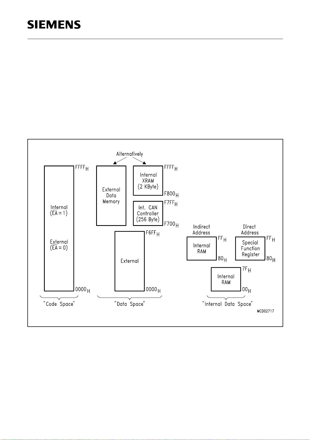
Memory Organization
3 Memory Organization
The C515C CPU manipulates operands in the following four address spaces:
– up to 64 Kbyte of internal/external program memory
– up to 64 Kbyte of external data memory
– 256 bytes of internal data memory
– 256 bytes CAN controller registers / data memory
– 2K bytes of internal XRAM data memory
– a 128 byte special function register area
Figure 3-1 illustrates the memory address spaces of the C515C.
C515C
Figure 3-1
C515C Memory Map
Semiconductor Group 3-1 1997-10-01
Page 26

Memory Organization
C515C
3.1 Program Memory, "Code Space"
The C515C-8R provides 64 Kbytes of read-only program memory while the C515C-L has no
internal program memory. The C515C-8E provides 64 Kbytes of OTP program memory.. For
internal ROM/OTP program execution the EA pin must be put to high level. The 64K bytes program
memory can also be located completely external. If the EA pin is held low, the C515C fetches all
instructions from an external program memory.
3.2 Data Memory, "Data Space"
The data memory address space consists of an internal and an external memory space. The
internal data memory is divided into three physically separate and distinct blocks : the lower 128
bytes of RAM, the upper 128 bytes of RAM, and the 128 byte special function register (SFR) area.
While the upper 128 bytes of data memory and the SFR area share the same address locations,
they are accessed through different addressing modes. The lower 128 bytes of data memory can
be accessed through direct or register indirect addressing; the upper 128 bytes of RAM can be
accessed through register indirect addressing; the special function registers are accessible through
direct addressing. Four 8-register banks, each bank consisting of eight 8-bit multi-purpose registers,
occupy locations 0 through 1FH in the lower RAM area. The next 16 bytes, locations 20H through
2FH, contain 128 directly addressable bit locations. The stack can be located anywhere in the
internal data memory address space, and the stack depth can be expanded up to 256 bytes.
The external data memory can be expanded up to 64 Kbyte and can be accessed by instructions
that use a 16-bit or an 8-bit address. The internal CAN controller and the internal XRAM are located
in the external address memory area at addresses F700H to FFFFH. Using MOVX instruction with
addresses pointing to this address area, alternatively XRAM and CAN controller registers or
external XRAM are accessed.
3.3 General Purpose Registers
The lower 32 locations of the internal RAM are assigned to four banks with eight general purpose
registers (GPRs) each. Only one of these banks may be enabled at a time. Two bits in the program
status word, RS0 (PSW.3) and RS1 (PSW.4), select the active register bank (see description of the
PSW in chapter 2). This allows fast context switching, which is useful when entering subroutines
or interrupt service routines.
The 8 general purpose registers of the selected register bank may be accessed by register
addressing. With register addressing the instruction op code indicates which register is to be used.
For indirect addressing R0 and R1 are used as pointer or index register to address internal or
external memory (e.g. MOV @R0).
Reset initializes the stack pointer to location 07H and increments it once to start from location 08
which is also the first register (R0) of register bank 1. Thus, if one is going to use more than one
register bank, the SP should be initialized to a different location of the RAM which is not used for
data storage.
H
Semiconductor Group 3-2 1997-10-01
Page 27
Memory Organization
C515C
3.4 XRAM Operation
The XRAM in the C515C is a memory area that is logically located at the upper end of the external
memory space, but is integrated on the chip. Because the XRAM is used in the same way as
external data memory the same instruction types (MOVX) must be used for accessing the XRAM.
3.4.1 XRAM/CAN Controller Access Control
Two bits in SFR SYSCON, XMAP0 and XMAP1, control the accesses to XRAM and the CAN
controller. XMAP0 is a general access enable/disable control bit and XMAP1 controls the external
signal generation during XRAM/CAN controller accesses.
Special Function Register SYSCON (Address B1H) Reset Value C515C-8R : X010XX01
Reset Value C515C-8E : X010X001
Bit No. MSB LSB
76543210
B1
H
Bit Function
– Not implemented. Reserved for future use.
XMAP1 XRAM/CAN controller visible access control
– PMOD
The function of the shaded bit is not described in this section.
Control bit for RD
addresses are outside the XRAM/CAN controller address range or if
XRAM is disabled, this bit has no effect.
XMAP1 = 0 : The signals RD and WR are not activated during accesses to
XMAP1 = 1 : Ports 0, 2 and the signals RD and WR are activated during
EALE RMAP –
/WR signals during XRAM/CAN Controller accesses. If
the XRAM/CAN Controller
accesses to XRAM/CAN Controller. In this mode, address
and data information during XRAM/CAN Controller accesses
are visible externally.
CSWO XMAP1
XMAP0
SYSCON
B
B
XMAP0 Global XRAM/CAN controller access enable/disable control
XMAP0 = 0 : The access to XRAM and CAN controller is enabled.
XMAP0 = 1 : The access to XRAM and CAN controller is disabled (default
after reset!). All MOVX accesses are performed via the
external bus. Further, this bit is hardware protected.
When bit XMAP1 in SFR SYSCON is set, during all accesses to XRAM and CAN Controller RD and
WR become active and port 0 and 2 drive the actual address/data information which is read/written
from/to XRAM or CAN controller. This feature allows to check the internal data transfers to XRAM
and CAN controller. When port 0 and 2 are used for I/O purposes, the XMAP1 bit should not be set.
Otherwise the I/O function of the port 0 and port 2 lines is interrupted.
Semiconductor Group 3-3 1997-10-01
Page 28

Memory Organization
C515C
After a reset operation, bit XMAP0 is reset. This means that the accesses to XRAM and CAN
controller are generally disabled. In this case, all accesses using MOVX instructions within the
address range of F700H to FFFFH generate external data memory bus cycles. When XMAP0 is set,
the access to XRAM and CAN controller is enabled and all accesses using MOVX instructions with
an address in the range of F700H to FFFFH will access internal XRAM or CAN controller.
Bit XMAP0 is hardware protected. If it is reset once (XRAM and CAN controller access enabled) it
cannot be set by software. Only a reset operation will set the XMAP0 bit again. This hardware
protection mechanism is done by an unsymmetric latch at XMAP0 bit. A unintentional disabling of
XRAM and CAN controller could be dangerous since indeterminate values could be read from the
external bus. To avoid this the XMAP0 bit is forced to '1' only by a reset operation. Additionally,
during reset an internal capacitor is loaded. So the reset state is a disabled XRAM and CAN
controller. Because of the load time of the capacitor, XMAP0 bit once written to '0' (that is,
discharging the capacitor) cannot be set to '1' again by software. On the other hand any distortion
(software hang up, noise,...) is not able to load this capacitor, too. That is, the stable status is XRAM
and CAN controller enabled.
The clear instruction for the XMAP0 bit should be integrated in the program initialization routine
before XRAM or CAN controller is used. In extremely noisy systems the user may have redundant
clear instructions.
Semiconductor Group 3-4 1997-10-01
Page 29

Memory Organization
C515C
3.4.2 Accesses to XRAM using the DPTR (16-bit Addressing Mode)
The XRAM and CAN controller can be accessed by two read/write instructions, which use the 16bit DPTR for indirect addressing. These instructions are :
– MOVX A, @DPTR (Read)
– MOVX @DPTR, A (Write)
For accessing the XRAM, the effective address stored in DPTR must be in the range of F800H to
FFFFH. For accessing the CAN controller, the effective address stored in DPTR must be in the
range of F700H to F7FFH.
3.4.3 Accesses to XRAM using the Registers R0/R1 (8-bit Addressing Mode)
The 8051 architecture provides also instructions for accesses to external data memory range which
use only an 8-bit address (indirect addressing with registers R0 or R1). The instructions are:
MOVX A, @ Ri (Read)
MOVX @Ri, A (Write)
As in the SAB 80C515A a special page register is implemented into the C515C to provide the
possibility of accessing the XRAM or CAN controller also with the MOVX @Ri instructions, i.e.
XPAGE serves the same function for the XRAM and CAN controller as Port 2 for external data
memory.
Special Function Register XPAGE (Address 91H) Reset Value : 00
Bit No. MSB LSB
76543210
91
H
Bit Function
XPAGE.7-0 XRAM/CAN controller high address
XPAGE.7-0 is the address part A15-A8 when 8-bit MOVX instructions are
used to access internal XRAM or CAN controller.
.5 .4 .3
.2 .1.7 .6 .0
XPAGE
H
Figures 3-2 to 3-4 show the dependencies of XPAGE- and Port 2 - addressing in order to explain
the differences in accessing XRAM/CAN controller, ext. RAM or what is to do when Port 2 is used
as an I/O-port.
Semiconductor Group 3-5 1997-10-01
Page 30
Memory Organization
C515C
Port 0
XRAM
CAN-Controller
XPAGE
Write to
Port 2
Port 2 Page Address
Address/Data
MCS02761
Figure 3-2
Write Page Address to Port 2
“MOV P2,pageaddress“ will write the page address to Port 2 and the XPAGE-Register.
When external RAM is to be accessed in the XRAM/CAN controller address range (F700H -
FFFFH), the XRAM/CAN controller has to be disabled. When additional external RAM is to be
addressed in an address range < F700H, the XRAM/CAN controller may remain enabled and there
is no need to overwrite XPAGE by a second move.
Semiconductor Group 3-6 1997-10-01
Page 31

Memory Organization
C515C
Port 0
XRAM
CAN-Controller
XPAGE
Write to
XPAGE
Port 2
Address/Data
Address/
I/O Data
MCS02762
Figure 3-3
Write Page Address to XPAGE
The page address is only written to the XPAGE register. Port 2 is available for addresses or I/O
data.
Semiconductor Group 3-7 1997-10-01
Page 32
Memory Organization
C515C
Port 0
XRAM
CAN-Controller
XPAGE
Write
I/O Data
to Port 2
Port 2 I/O Data
Address/Data
MCS02763
Figure 3-4
Use of Port 2 as I/O Port
At a write to port 2, the XRAM/CAN controller address in XPAGE register will be overwritten
because of the concurrent write to port 2 and XPAGE register. So, whenever XRAM is used and the
XRAM address differs from the byte written to port 2 latch it is absolutely necessary to rewrite
XPAGE with the page address.
Example :
I/O data at port 2 shall be AAH. A byte shall be fetched from XRAM at address F830H.
MOV R0, #30H ;
MOV P2, #0AAH ; P2 shows AAH and XPAGE contains AAH
MOV XPAGE, #0F8H ; P2 still shows AAH but XRAM is addressed
MOVX A, @R0 ; the contents of XRAM at F830H is moved to accumulator
Semiconductor Group 3-8 1997-10-01
Page 33

Memory Organization
C515C
The register XPAGE provides the upper address byte for accesses to XRAM with MOVX @Ri
instructions. If the address formed by XPAGE and Ri points outside the XRAM/CAN Controller
address range, an external access is performed. For the C515C the content of XPAGE must be
greater or equal F7H in order to use the XRAM/CAN Controller.
The software has to distinguish two cases, if the MOVX @Ri instructions with paging shall be used :
a) Access to XRAM/CAN Contr. :The upper address byte must be written to XPAGE or P2;
both writes select the XRAM/CAN controller address range.
b) Access to external memory : The upper address byte must be written to P2; XPAGE will be
loaded with the same address in order to deselect the XRAM.
3.4.4 Reset Operation of the XRAM
The contents of the XRAM is not affected by a reset. After power-up the contents are undefined,
while they remain unchanged during and after a reset as long as the power supply is not turned off.
If a reset occurs during a write operation to XRAM, the content of a XRAM memory location
depends on the cycle in which the active reset signal is detected (MOVX is a 2-cycle instruction):
Reset during 1st cycle : The new value will not be written to XRAM. The old value is not affected.
Reset during 2nd cycle : The old value in XRAM is overwritten by the new value.
3.4.5 Behaviour of Port0 and Port2
The behaviour of Port 0 and P2 during a MOVX access depends on the control bits in register
SYSCON and on the state of pin EA. The table 3-1 lists the various operating conditions. It shows
the following characteristics:
a) Use of P0 and P2 pins during the MOVX access.
Bus: The pins work as external address/data bus. If (internal) XRAM is accessed, the data
written to the XRAM can be seen on the bus in debug mode.
I/0: The pins work as Input/Output lines under control of their latch.
b) Activation of the RD and WR pin during the access.
c) Use of internal or external XDATA memory.
The shaded areas describe the standard operation as each 80C51 device without on-chip XRAM
behaves.
Semiconductor Group 3-9 1997-10-01
Page 34
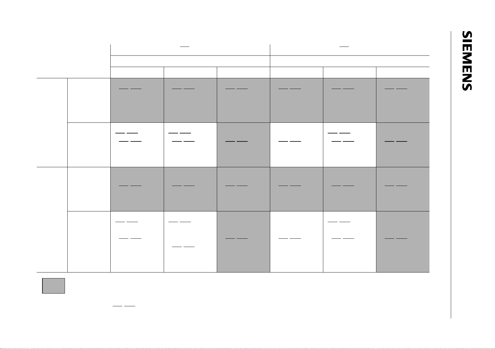
Semiconductor Group 3-10 1997-10-01
= 0 EA = 1
EA
XMAP1, XMAP0 XMAP1, XMAP0
00 10 X1 00 10 X1
MOVX
@DPTR
MOVX
@ Ri
Table 3-1
Behaviour of P0/P2 and RD
DPTR
<
XRAM
address
range
DPTR
≥
XRAM
address
range
XPAGE
<
XRAM
addr.page
range
XPAGE
≥
XRAM
addr.page
range
modes compatible to 8051/C501 family
a)P0/P2→Bus
b)RD/WR active
c)ext.memory
is used
a)P0/P2
(RD/WR-Data)
b)RD/WR
inactive
c)XRAM is used
a)P0→Bus
P2→I/O
b)RD/WR active
c)ext.memory
is used
a)P0
(RD/WR-Data)
P2→I/O
b)RD/WR
inactive
c)XRAM is used
a)P0/P2→Bus
b)RD/WR active
c)ext.memory
is used
→Bus
→Bus
/WR During MOVX Accesses
a)P0/P2→Bus
(RD/WR-Data)
b)RD/WR active
c)XRAM is used
a)P0→Bus
P2→I/O
b)RD/WR active
c)ext.memory
is used
a)P0→Bus
(RD/WR-Data
only)
P2→I/O
b)RD/WR active
c)XRAM is used
a)P0/P2→Bus
b)RD/WR active
c)ext.memory
is used
a)P0/P2→Bus
b)RD/WR active
c) ext.memory
is used
a)P0→Bus
P2→I/O
b)RD/WR active
c)ext.memory
is used
a)P0→Bus
P2→I/O
b)RD/WR active
c)ext.memory
is used
a)P0/P2→Bus
b)RD/WR active
c)ext.memory
is used
a)P0/P2→I/0
b)RD/WR
inactive
c)XRAM is used
a)P0→Bus
P2→I/O
b)RD/WR active
c)ext.memory
is used
a)P2→I/O
P0/P2→I/O
b)RD/WR
inactive
c)XRAM is used
a)P0/P2→Bus
b)RD/WR active
c)ext.memory
is used
a)P0/P2→Bus
(RD/WR-Data)
b)RD/WR active
c)XRAM is used
a)P0→Bus
P2→I/O
b)RD/WR active
c)ext.memory
is used
a)P0→Bus
(RD/WR-Data)
P2→I/O
b)RD/WR active
c)XRAM is used
a)P0/P2→Bus
b)RD/WR active
c)ext.memory
is used
a)P0/P2→Bus
b)RD/WR active
c) ext.memory
is used
a)P0→Bus
P2→I/O
b)RD/WR active
c)ext.memory
is used
a)P0→Bus
P2→I/O
Memory Organization
b)RD/WR active
c)ext.memory
is used
C515C
Page 35

Memory Organization
C515C
3.5 Special Function Registers
The registers, except the program counter and the four general purpose register banks, reside in
the special function register area. The special function register area consists of two portions : the
standard special function register area and the mapped special function register area. Two special
function registers of the C515C (PCON1 and DIR5) are located in the mapped special function
register area. For accessing the mapped special function register area, bit RMAP in special function
register SYSCON must be set. All other special function registers are located in the standard
special function register area which is accessed when RMAP is cleared (“0“).
The registers and data locations of the CAN controller (CAN-SFRs) are located in the external data
memory area at addresses F700H to F7FFH. Details about the access of these registers is
described in section 3.4.1 of this chapter.
Special Function Register SYSCON (Address B1H) Reset Value C515C-8R : X010XX01
Reset Value C515C-8E : X010X001
Bit No. MSB LSB
76543210
B1
H
Bit Function
– Reserved bits for future use.
RMAP Special function register map bit
As long as bit RMAP is set, mapped special function register area can be accessed. This bit is not
cleared by hardware automatically. Thus, when non-mapped/mapped registers are to be accessed,
the bit RMAP must be cleared/set by software, respectively each.
– PMOD
The functions of the shaded bits are not described in this section.
RMAP = 0 : The access to the non-mapped (standard) special function
RMAP = 1 : The access to the mapped special function register area is
EALE RMAP –
register area is enabled.
enabled.
CSWO XMAP1
XMAP0
SYSCON
B
B
All SFRs with addresses where address bits 0-2 are 0 (e.g. 80H, 88H, 90H, 98H, ..., F8H, FFH) are
bitaddressable.
The 59 special function registers (SFRs) in the standard and mapped SFR area include pointers
and registers that provide an interface between the CPU and the other on-chip peripherals. The
SFRs of the C515C are listed in table 3-2 and table 3-3. In table 3-2 they are organized in groups
which refer to the functional blocks of the C515C. The CAN-SFRs are also included in table 3-2.
Table 3-3 illustrates the contents of the SFRs in numeric order of their addresses. Table 3-4 list the
CAN-SFRs in numeric order of their addresses. .
Semiconductor Group 3-11 1997-10-01
Page 36

Memory Organization
C515C
Table 3-2
Special Function Registers - Functional Blocks
Block Symbol Name Address Contents after
Reset
CPU ACC
B
DPH
DPL
DPSEL
PSW
SP
SYSCON
A/DConverter
ADCON0
ADCON1
ADDATH
ADDATL
Interrupt
System
IEN0
IEN1
2)
2)
IEN2
2)
IP0
IP1
TCON
T2CON
SCON
IRCON
XRAM XPAGE
2)
Accumulator
B-Register
Data Pointer, High Byte
Data Pointer, Low Byte
Data Pointer Select Register
Program Status Word Register
Stack Pointer
2)
System Control Register C515C-8R
2)
A/D Converter Control Register 0
A/D Converter Control Register 1
A/D Converter Data Register High Byte
A/D Converter Data Register Low Byte
Interrupt Enable Register 0
Interrupt Enable Register 1
Interrupt Enable Register 2
Interrupt Priority Register 0
Interrupt Priority Register 1
2)
Timer Control Register
2)
Timer 2 Control Register
Serial Channel Control Register
Interrupt Request Control Register
Page Address Register for Extended on-chip
C515C-8E
E0
F0
83
82
92
D0
81
B1
B1
D8
DC
D9
DA
A8
B8
9A
A9
B9
88
C8
98
C0
91
H
H
H
H
H
H
H
H
H
H
H
H
H
H
H
H
H
H
H
H
H
1)
1)
1)
1)
H
H
1)
1)
1)
1)
1)
1)
XRAM and CAN Controller
2)
SYSCON
System Control Register C515C-8R
C515C-8E
Ports P0
P1
P2
P3
P4
P5
DIR5
P6
P7
SYSCON
Port 0
Port 1
Port 2
Port 3
Port 4
Port 5
Port 5 Direction Register
Port 6, Analog/Digital Input
Port 7
2)
System Control Register C515C-8R
C515C-8E
1) Bit-addressable special function registers
2) This special function register is listed repeatedly since some bits of it also belong to other functional blocks.
3) “X“ means that the value is undefined and the location is reserved
4) This SFR is a mapped SFR. For accessing this SFR, bit PDIR in SFR IP1 must be set.
B1
B1
80
90
A0
B0
E8
F8
F8
DB
FA
B1
B1
H
H
H
H
H
H
H
H
H
H
H
H
1)
1)
1)
1
1)
1)
1) 4)
H
4)
00
H
00
H
00
H
00
H
XXXXX000
00
H
07
H
X010XX01
X010X001
00
H
0XXXX000
00
H
00XXXXXX
00
H
00
H
XX00X00X
00
H
0X000000
00
H
00
H
00
H
00
H
00
H
X010XX01
X010X001
FF
H
FF
H
FF
H
FF
H
FF
H
FF
H
FF
H
–
XXXXXXX1
X010XX01
X010X001
3)
B
3)
B
3)
B
3)
B
3)
B
3)
B
3)
B
3)
B
3)
B
3)
B
3)
B
3)
B
Semiconductor Group 3-12 1997-10-01
Page 37

Memory Organization
C515C
Table 3-2
Special Function Registers - Functional Blocks (cont’d)
Block Symbol Name Address Contents after
Reset
Serial
Channel
ADCON0
PCON
SBUF
SCON
SRELL
SRELH
CAN
ControllerCRSR
IR
BTR0
BTR1
GMS0
GMS1
UGML0
UGML1
LGML0
LGML1
UMLM0
UMLM1
LMLM0
LMLM1
2)
A/D Converter Control Register 0
2)
Power Control Register
Serial Channel Buffer Register
Serial Channel Control Register
Serial Channel Reload Register, low byte
Serial Channel Reload Register, high byte
Control Register
Status Register
Interrupt Register
Bit Timing Register Low
Bit Timing Register High
Global Mask Short Register Low
Global Mask Short Register High
Upper Global Mask Long Register Low
Upper Global Mask Long Register High
Lower Global Mask Long Register Low
Lower Global Mask Long Register High
Upper Mask of Last Message Register Low
Upper Mask of Last Message Register High
Lower Mask of Last Message Register Low
Lower Mask of Last Message Register High
Message Object Registers :
MCR0
MCR1
UAR0
UAR1
LAR0
LAR1
MCFG
DB0
DB1
DB2
DB3
DB4
DB5
DB6
DB7
1) Bit-addressable special function registers
2) This special function register is listed repeatedly since some bits of it also belong to other functional blocks.
3) “X“ means that the value is undefined and the location is reserved. “U“ means that the value is unchanged by
a reset operation. “U“ values are undefined (as “X“) after a power-on reset operation
4) SFR is located in the mapped SFR area. For accessing this SFR, bit RMAP in SFR SYSCON must be set.
5) The notation “n“ in the message object address definition defines the number of the related message object.
Message Control Register Low
Message Control Register High
Upper Arbitration Register Low
Upper Arbitration Register High
Lower Arbitration Register Low
Lower Arbitration Register High
Message Configuration Register
Message Data Byte 0
Message Data Byte 1
Message Data Byte 2
Message Data Byte 3
Message Data Byte 4
Message Data Byte 5
Message Data Byte 6
Message Data Byte 7
D8
H
87
H
99
H
98
H
AA
H
BA
H
F700
F701
F702
F704
F705
F706
F707
F708
F709
F70A
F70B
F70C
F70D
F70E
F70F
F7n0
F7n1
F7n2
F7n3
F7n4
F7n5
F7n6
F7n7
F7n8
F7n9
F7nA
F7nB
F7nC
F7nD
F7nE
1
1)
H
H
H
H
H
H
H
H
H
H
H
H
H
H
H
H
H
H
H
H
H
H
H
H
H
H
H
H
H
H
5)
5)
5)
5)
5)
5)
5)
5)
5)
5)
5)
5)
5)
5)
5)
00
H
00
H
3)
XX
H
00
H
D9
H
XXXXXX11
01
H
3)
XX
H
3)
XX
H
3)
UU
H
0UUUUUUU
3)
UU
H
UUU11111
3)
UU
H
3)
UU
H
3)
UU
H
UUUUU000
3)
UU
H
3)
UU
H
3)
UU
H
UUUUU000
3)
UU
H
3)
UU
H
3)
UU
H
3)
UU
H
3)
UU
H
UUUUU000
UUUUUU00
3)
XX
H
3)
XX
H
3)
XX
H
3)
XX
H
3)
XX
H
3)
XX
H
3)
XX
H
3)
XX
H
3)
B
3)
B
3)
B
3)
B
3)
B
3)
B
3)
B
Semiconductor Group 3-13 1997-10-01
Page 38

Memory Organization
C515C
Table 3-2
Special Function Registers - Functional Blocks (cont’d)
Block Symbol Name Address Contents after
Reset
)
SSC
Interface
Timer 0/
Timer 1
Compare/
Capture
Unit /
Timer 2
Watchdog WDTREL
Power
Save
Modes
1) Bit-addressable special function registers
2) This special function register is listed repeatedly since some bits of it also belong to other functional blocks.
3) “X“ means that the value is undefined and the location is reserved
4) SFR is located in the mapped SFR area. For accessing this SFR, bit RMAP in SFR SYSCON must be set.
SSCCON
STB
SRB
SCF
SCIEN
SSCMOD
TCON
TH0
TH1
TL0
TL1
TMOD
CCEN
CCH1
CCH2
CCH3
CCL1
CCL2
CCL3
CRCH
CRCL
TH2
TL2
T2CON
2)
IEN0
2)
IEN1
2)
IP0
PCON
2)
PCON1
SSC Control Register
SSC Transmit Buffer
SSC Receive Register
SSC Flag Register
SSC Interrupt Enable Register
SSC Mode Test Register
Timer 0/1 Control Register
Timer 0, High Byte
Timer 1, High Byte
Timer 0, Low Byte
Timer 1, Low Byte
Timer Mode Register
Comp./Capture Enable Reg.
Comp./Capture Reg. 1, High Byte
Comp./Capture Reg. 2, High Byte
Comp./Capture Reg. 3, High Byte
Comp./Capture Reg. 1, Low Byte
Comp./Capture Reg. 2, Low Byte
Comp./Capture Reg. 3, Low Byte
Com./Rel./Capt. Reg. High Byte
Com./Rel./Capt. Reg. Low Byte
Timer 2, High Byte
Timer 2, Low Byte
Timer 2 Control Register
Watchdog Timer Reload Register
Interrupt Enable Register 0
Interrupt Enable Register 1
Interrupt Priority Register 0
Power Control Register
Power Control Register 1 C515C-8R
C515C-8E
93
94
95
AB
AC
96
88
8C
8D
8A
8B
89
C1
C3
C5
C7
C2
C4
C6
CB
CA
CD
CC
C8
86
A8
B8
A9
87
88
88
H
H
H
H
H
H
H
H
H
H
H
H
H
H
H
H
H
H
H
H
H
H
H
H
H
H
H
H
H
H
H
1
1
1)
1)
1)
1)
4)
4)
)
07
H
3
XX
)
H
3
XX
)
H
XXXXXX00
XXXXXX00
00
H
00
H
00
H
00
H
00
H
00
H
00
H
00
H
00
H
00
H
00
H
00
H
00
H
00
H
00
H
00
H
00
H
00
H
00
H
00
H
00
H
00
H
00
H
00
H
0XXXXXXX
0XX0XXXX
3)
B
3)
B
3)
B
3)
B
Semiconductor Group 3-14 1997-10-01
Page 39
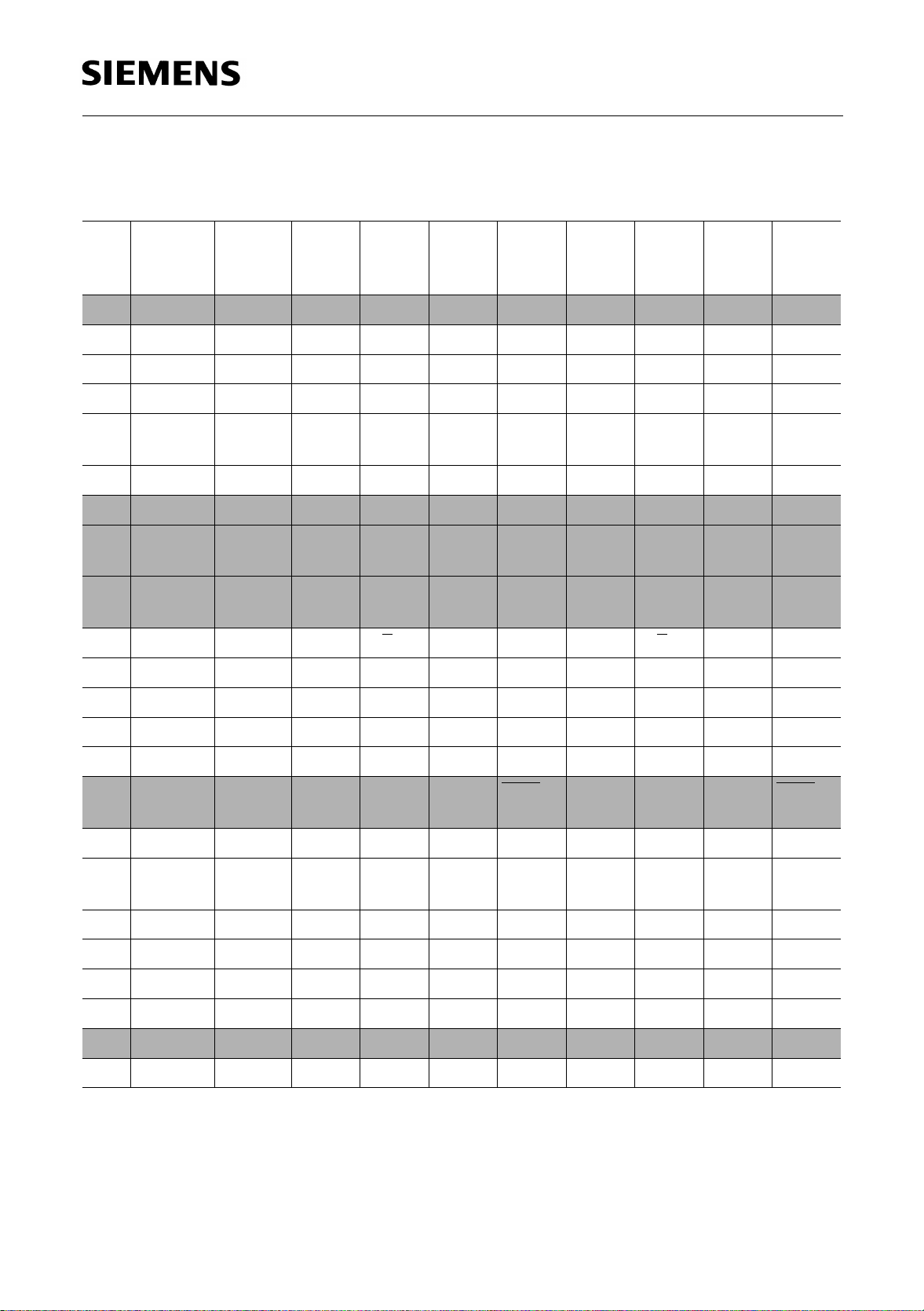
Table 3-3
Contents of the SFRs, SFRs in numeric order of their addresses
Memory Organization
C515C
Addr Register Content
after
Reset
2)
80
81
82
83
86
87
88
88
P0 FF
H
SP 07
H
DPL 00
H
DPH 00
H
WDTREL 00
H
PCON 00
H
2)
TCON 00
H
3)
PCON1
H
4)
0XXXXXXX
88
H
3)
PCON1
5)
0XX0XXXX
89
TMOD 00
H
8AHTL0 00
8BHTL1 00
8CHTH0 00
8DHTH1 00
2)
90
P1 FF
H
1)
H
H
H
H
H
H
H
B
B
H
H
H
H
H
H
Bit 7 Bit 6 Bit 5 Bit 4 Bit 3 Bit 2 Bit 1 Bit 0
.7 .6 .5 .4 .3 .2 .1 .0
.7 .6 .5 .4 .3 .2 .1 .0
.7 .6 .5 .4 .3 .2 .1 .0
.7 .6 .5 .4 .3 .2 .1 .0
WDT
.6 .5 .4 .3 .2 .1 .0
PSEL
SMOD PDS IDLS SD GF1 GF0 PDE IDLE
TF1 TR1 TF0 TR0 IE1 IT1 IE0 IT0
EWPD – – – – – – –
EWPD – – WS – – – –
GATE C/T
M1 M0 GATE C/T M1 M0
.7 .6 .5 .4 .3 .2 .1 .0
.7 .6 .5 .4 .3 .2 .1 .0
.7 .6 .5 .4 .3 .2 .1 .0
.7 .6 .5 .4 .3 .2 .1 .0
T2 CLK-
T2EX INT2 INT6 INT5 INT4 INT3
OUT
91
92
93
94
95
96
98
99
1) X means that the value is undefined and the location is reserved
2) Bit-addressable special function registers
3) SFR is located in the mapped SFR area. For accessing this SFR, bit RMAP in SFR SYSCON must be set.
4) This SFR is available in the C515C-8R and C515C-L.
5) This SFR is available in the C515C-8E.
XPAGE 00
H
DPSEL XXXX-
H
SSCCON
H
STB XX
H
SRB XX
H
SSCMOD
H
2)
SCON 00
H
SBUF XX
H
H
X000
07
H
H
H
00
H
H
H
.7 .6 .5 .4 .3 .2 .1 .0
–––––.2.1.0
B
SCEN TEN MSTR CPOL CPHA BRS2 BRS1 BRS0
.7 .6 .5 .4 .3 .2 .1 .0
.7 .6 .5 .4 .3 .2 .1 .0
LOOPB
TRIO 00000LSBSM
SM0 SM1 SM2 REN TB8 RB8 TI RI
.7 .6 .5 .4 .3 .2 .1 .0
Semiconductor Group 3-15 1997-10-01
Page 40
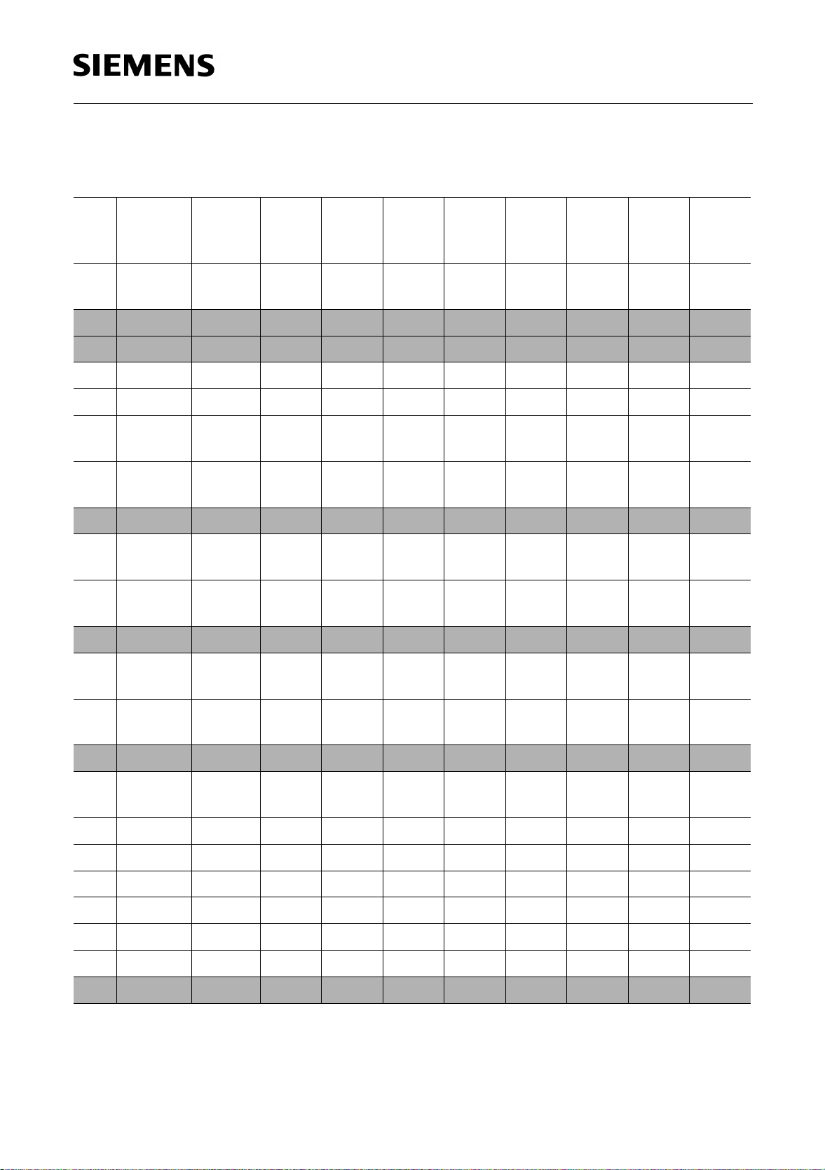
Memory Organization
Table 3-3
Contents of the SFRs, SFRs in numeric order of their addresses (cont’d)
C515C
Addr Register Content
after
Reset
1)
9AHIEN2 X00X-
X00X
B
2)
A0
A8
A9HIP0 00
AAHSRELL D9
P2 FF
H
2)
IEN0 00
H
H
H
H
H
ABHSCF XXXX-
XX00
B
ACHSCIEN XXXX-
XX00
B
2)
B0
B1HSYSCON
B1HSYSCON
B8
P3 FF
H
3)
4)
2)
IEN1 00
H
H
X010XX01
X010X001
H
B
B
B9HIP1 0X00-
0000
B
BAHSRELH XXXX-
XX11
B
2)
C0
C1HCCEN 00
IRCON 00
H
H
H
Bit 7 Bit 6 Bit 5 Bit 4 Bit 3 Bit 2 Bit 1 Bit 0
– – EX8 EX7 – ESSC ECAN –
.7 .6 .5 .4 .3 .2 .1 .0
EAL WDT ET2 ES ET1 EX1 ET0 EX0
OWDS WDTS .5 .4 .3 .2 .1 .0
.7 .6 .5 .4 .3 .2 .1 .0
––––––WCOL TC
––––––WCEN TCEN
RD WR T1 T0 INT1 INT0 TxD RxD
– PMOD EALE RMAP – – XMAP1 XMAP0
– PMOD EALE RMAP – CSWO XMAP1 XMAP0
EXEN2 SWDT EX6 EX5 EX4 EX3 EX2 EADC
PDIR – .5 .4 .3 .2 .1 .0
––––––.1.0
EXF2 TF2 IEX6 IEX5 IEX4 IEX3 IEX2 IADC
COCAH3COCAL3COCAH2COCAL2COCAH1COCAL1COCAH0COCAL
0
C2HCCL1 00
C3HCCH1 00
C4HCCL2 00
C5HCCH2 00
C6HCCL3 00
C7HCCH3 00
2)
C8
1) X means that the value is undefined and the location is reserved
2) Bit-addressable special function registers
3) This SFR is available in the C515C-8R and C515C-L.
4) This SFR is available in the C515C-8E.
T2CON 00
H
H
H
H
H
H
H
H
.7 .6 .5 .4 .3 .2 .1 .0
.7 .6 .5 .4 .3 .2 .1 .0
.7 .6 .5 .4 .3 .2 .1 .0
.7 .6 .5 .4 .3 .2 .1 .0
.7 .6 .5 .4 .3 .2 .1 .0
.7 .6 .5 .4 .3 .2 .1 .0
T2PS I3FR I2FR T2R1 T2R0 T2CM T2I1 T2I0
Semiconductor Group 3-16 1997-10-01
Page 41
Memory Organization
Table 3-3
Contents of the SFRs, SFRs in numeric order of their addresses (cont’d)
C515C
Addr Register Content
Bit 7 Bit 6 Bit 5 Bit 4 Bit 3 Bit 2 Bit 1 Bit 0
after
H
H
H
H
H
H
H
1)
.7 .6 .5 .4 .3 .2 .1 .0
.7 .6 .5 .4 .3 .2 .1 .0
.7 .6 .5 .4 .3 .2 .1 .0
.7 .6 .5 .4 .3 .2 .1 .0
CY AC F0 RS1 RS0 OV F1 P
BD CLK ADEX BSY ADM MX2 MX1 MX0
.9 .8 .7 .6 .5 .4 .3 .2
.1.0––––––
B
Reset
CAHCRCL 00
CBHCRCH 00
CCHTL2 00
CDHTH2 00
2)
D0
D8
PSW 00
H
2)
ADCON0 00
H
D9HADDATH 00
DAHADDATL 00XX-
XXXX
DBHP6 – .7.6.5.4.3.2.1.0
DCHADCON1 0XXX-
X000
2)
E0
E8
F0
F8
F8
ACC 00
H
2)
P4 FF
H
2)
B 00
H
2)
P5 FF
H
2)
DIR5
H
H
H
H
H
3)
FF
H
FAHP7 XXXX-
XXX1
FCHVR0
FDHVR1
FEHVR2
4) 5)
4) 5)
4) 5) 6)
C5
95
H
H
ADCL –––0MX2MX1MX0
B
.7 .6 .5 .4 .3 .2 .1 .0
RXDC TXDC INT8 SLS STO SRI SCLK ADST
.7 .6 .5 .4 .3 .2 .1 .0
.7 .6 .5 .4 .3 .2 .1 .0
.7 .6 .5 .4 .3 .2 .1 .0
–––––––INT7
B
11000101
10010101
.7 .6 .5 .4 .3 .2 .1 .0
1) X means that the value is undefined and the location is reserved
2) Bit-addressable special function registers
3) This SFR is a mapped SFR. For accessing this SFR, bit PDIR in SFR IP1 must be set.
4) This SFR is a mapped SFR. For accessing this SFR, bit RMAP in SFR SYSCON must be set.
5) These SFRs are read-only registers (C515C-8E only).
6) The content of this SFR varies with the actual step of the C515C-8E (see also chapter 10-7).
Semiconductor Group 3-17 1997-10-01
Page 42

Memory Organization
Table 3-4
Contents of the CAN Registers in numeric order of their addresses
C515C
Addr.
n=1-F
F700
F701
F702
F704
F705
F706
F707
F708
F709
F70A
F70B
F70C
F70D
F70E
F70F
F7n0
F7n1
Register Content
1)
H
CR 01
H
SR XX
H
IR XX
H
BTR0 UU
H
BTR1 0UUU.
H
GMS0 UU
H
GMS1 UUU1.
H
UGML0 UU
H
UGML1 UU
H
LGML0 UU
H
LGML1 UUUU.
H
UMLM0 UU
H
UMLM1 UU
H
LMLM0 UU
H
LMLM1 UUUU.
H
MCR0 UU
H
MCR1 UU
H
after
Reset
H
H
H
H
UUUU
H
1111
B
H
H
H
U000
H
H
H
U000
H
H
Bit 7 Bit 6 Bit 5 Bit 4 Bit 3 Bit 2 Bit 1 Bit 0
2)
TEST CCE 0 0 EIE SIE IE INIT
BOFF EWRN – RXOK TXOK LEC2 LEC1 LEC0
INTID
SJW BRP
0 TSEG2 TSEG1
B
ID28-21
ID20-18 11111
ID28-21
ID20-13
ID12-5
ID4-0 0 0 0
B
ID28-21
ID20-18 ID17-13
ID12-5
ID4-0 0 0 0
B
MSGVAL TXIE RXIE INTPND
RMTPND TXRQ MSGLST
NEWDAT
CPUUPD
F7n2
F7n3
F7n4
F7n5
F7n6
1) The notation “n“ in the address definition defines the number of the related message object.
2) “X“ means that the value is undefined and the location is reserved. “U“ means that the value is unchanged by
a reset operation. “U“ values are undefined (as “X“) after a power-on reset operation
UAR0 UU
H
UAR1 UU
H
LAR0 UU
H
LAR1 UUUU.
H
MCFG UUUU.
H
H
H
H
U000
UU00
ID28-21
ID20-18 ID17-13
ID12-5
ID4-0 0 0 0
B
DLC DIR XTD 0 0
B
Semiconductor Group 3-18 1997-10-01
Page 43

Memory Organization
Table 3-4
Contents of the CAN Registers in numeric order of their addresses (cont’d)
C515C
Addr.
n=1-F
F7n7
F7n8
F7n9
F7nA
F7nB
F7nC
F7nD
F7nE
1) The notation “n“ in the address definition defines the number of the related message object.
2) “X“ means that the value is undefined and the location is reserved. “U“ means that the value is unchanged by
a reset operation. “U“ values are undefined (as “X“) after a power-on reset operation
Register Content
1)
H
DB0 XX
H
DB1 XX
H
DB2 XX
H
DB3 XX
H
DB4 XX
H
DB5 XX
H
DB6 XX
H
DB7 XX
H
after
Reset
H
H
H
H
H
H
H
H
Bit 7 Bit 6 Bit 5 Bit 4 Bit 3 Bit 2 Bit 1 Bit 0
2)
.7 .6 .5 .4 .3 .2 .1 .0
.7 .6 .5 .4 .3 .2 .1 .0
.7 .6 .5 .4 .3 .2 .1 .0
.7 .6 .5 .4 .3 .2 .1 .0
.7 .6 .5 .4 .3 .2 .1 .0
.7 .6 .5 .4 .3 .2 .1 .0
.7 .6 .5 .4 .3 .2 .1 .0
.7 .6 .5 .4 .3 .2 .1 .0
Semiconductor Group 3-19 1997-10-01
Page 44

External Bus Interface
C515C
4 External Bus Interface
The C515C allows for external memory expansion. The functionality and implementation of the
external bus interface is identical to the common interface for the 8051 architecture with one
exception : if the C515C is used in systems with no external memory the generation of the ALE
signal can be suppressed. Resetting bit EALE in SFR SYSCON register, the ALE signal will be
gated off. This feature reduces RFI emisions of the system.
4.1 Accessing External Memory
It is possible to distinguish between accesses to external program memory and external data
memory or other peripheral components respectively. This distinction is made by hardware:
accesses to external program memory use the signal PSEN (program store enable) as a read
strobe. Accesses to external data memory use RD and WR to strobe the memory (alternate
functions of P3.7 and P3.6). Port 0 and port 2 (with exceptions) are used to provide data and
address signals. In this section only the port 0 and port 2 functions relevant to external memory
accesses are described.
Fetches from external program memory always use a 16-bit address. Accesses to external data
memory can use either a 16-bit address (MOVX @DPTR) or an 8-bit address (MOVX @Ri).
4.1.1 Role of P0 and P2 as Data/Address Bus
When used for accessing external memory, port 0 provides the data byte time-multiplexed with the
low byte of the address. In this state, port 0 is disconnected from its own port latch, and the address/
data signal drives both FETs in the port 0 output buffers. Thus, in this application, the port 0 pins are
not open-drain outputs and do not require external pullup resistors.
During any access to external memory, the CPU writes FFH to the port 0 latch (the special function
register), thus obliterating whatever information the port 0 SFR may have been holding.
Whenever a 16-bit address is used, the high byte of the address comes out on port 2, where it is
held for the duration of the read or write cycle. During this time, the port 2 lines are disconnected
from the port 2 latch (the special function register).
Thus the port 2 latch does not have to contain 1s, and the contents of the port 2 SFR are not
modified.
If an 8-bit address is used (MOVX @Ri), the contents of the port 2 SFR remain at the port 2 pins
throughout the external memory cycle. This will facilitate paging. It should be noted that, if a port 2
pin outputs an address bit that is a 1, strong pullups will be used for the entire read/write cycle and
not only for two oscillator periods.
Semiconductor Group 4-1 1997-10-01
Page 45

External Bus Interface
C515C
a)
b)
ALE
PSEN
RD
P2
P0
One Machine Cycle One Machine Cycle
S1 S2 S3 S4 S5 S6 S1 S2 S3 S4 S5 S6
PCL
OUT
valid
PCH
OUT
INSTINPCL
OUT
PCL OUT
valid
PCH PCH
OUT
INST
IN
PCL OUT
PCL
OUT
valid
One Machine CycleOne Machine Cycle
PCH
INSTINPCL
PCH
OUT
INST
IN
PCL OUT
OUTOUT
OUT
PCL OUT
valid
(A)
without
MOVX
INST
IN
ALE
PSEN
RD
PCL
OUT
valid
PCH
OUT
INST
IN
DPL or Ri
P2
P0
OUT
INST
IN
PCL OUT
Figure 4-1
External Program Memory Execution
valid
DPH OUT OR
P2 OUT
DATA
IN
PCL
OUT
PCL OUT
valid
S6S5S4S3S2S1S6S5S4S3S2S1
(B)
with
MOVX
PCHPCH
OUT
INST
IN
MCD02575
Semiconductor Group 4-2 1997-10-01
Page 46

External Bus Interface
C515C
4.1.2 Timing
The timing of the external bus interface, in particular the relationship between the control signals
ALE, PSEN, RD, WR and information on port 0 and port 2, is illustated in figure 4-1 a) and b).
Data memory: in a write cycle, the data byte to be written appears on port 0 just before WR is
activated and remains there until after WR is deactivated. In a read cycle, the
incoming byte is accepted at port 0 before the read strobe is deactivated.
Program memory: Signal PSEN functions as a read strobe.
4.1.3 External Program Memory Access
The external program memory is accessed whenever signal EA is active (low): Due to the 64K
internal ROM, no mixed internal/external program memory execution is possible.
When the CPU is executing out of external program memory, all 8 bits of port 2 are dedicated to an
output function and may not be used for general-purpose I/O. The contents of the port 2 SFR
however is not affected. During external program memory fetches port 2 lines output the high byte
of the PC, and during accesses to external data memory they output either DPH or the port 2 SFR
(depending on whether the external data memory access is a MOVX @DPTR or a MOVX @Ri).
4.2 PSEN, Program Store Enable
The read strobe for external fetches is PSEN. PSEN is not activated for internal fetches. When the
CPU is accessing external program memory, PSEN is activated twice every cycle (except during a
MOVX instruction) no matter whether or not the byte fetched is actually needed for the current
instruction. When PSEN is activated its timing is not the same as for RD. A complete RD cycle,
including activation and deactivation of ALE and RD, takes 6 oscillator periods. A complete PSEN
cycle, including activation and deactivation of ALE and PSEN takes 3 oscillator periods. The
execution sequence for these two types of read cycles is shown in figure 4-1 a) and b).
4.3 Overlapping External Data and Program Memory Spaces
In some applications it is desirable to execute a program from the same physical memory that is
used for storing data. In the C515C the external program and data memory spaces can be
combined by AND-ing PSEN
low read strobe that can be used for the combined physical memory. Since the PSEN cycle is faster
than the RD cycle, the external memory needs to be fast enough to adapt to the PSEN cycle.
and RD. A positive logic AND of these two signals produces an active
Semiconductor Group 4-3 1997-10-01
Page 47

External Bus Interface
C515C
4.4 ALE, Address Latch Enable
The C515C allows to switch off the ALE output signal. If the internal ROM is used (EA=1) and ALE
is switched off by EALE=0, Then, ALE will only go active during external data memory accesses
(MOVX instructions). If EA=0, the ALE generation is always enabled and the bit EALE has no effect.
After a hardware reset the ALE generation is enabled.
Special Function Register SYSCON (Address B1H) Reset Value C515C-8R : X010XX01
Reset Value C515C-8E : X010X001
Bit No. MSB LSB
76543210
B1
H
Bit Function
– Reserved bits for future use.
EALE Enable ALE output
– PMOD
The function of the shaded bit is not described in this section.
EALE = 0 : ALE generation is disabled; disables ALE signal generation
EALE = 1 : ALE generation is enabled
If EA=0, the ALE generation is always enabled and the bit EALE has no
effect on the ALE generation.
EALE RMAP –
during internal code memory accesses (EA
ALE is automatically generated at MOVX instructions.
CSWO XMAP1
XMAP0
SYSCON
=1). With EA=1,
B
B
Semiconductor Group 4-4 1997-10-01
Page 48
External Bus Interface
C515C
4.5 Enhanced Hooks Emulation Concept
The Enhanced Hooks Emulation Concept of the C500 microcontroller family is a new, innovative
way to control the execution of C500 MCUs and to gain extensive information on the internal
operation of the controllers. Emulation of on-chip ROM based programs is possible, too.
Each production chip has built-in logic for the support of the Enhanced Hooks Emulation Concept.
Therefore, no costly bond-out chips are necessary for emulation. This also ensure that emulation
and production chips are identical.
The Enhanced Hooks TechnologyTM, which requires embedded logic in the C500 allows the C500
together with an EH-IC to function similar to a bond-out chip. This simplifies the design and reduces
costs of an ICE-system. ICE-systems using an EH-IC and a compatible C500 are able to emulate
all operating modes of the different versions of the C500 microcontrollers. This includes emulation
of ROM, ROM with code rollover and ROMless modes of operation. It is also able to operate in
single step mode and to read the SFRs after a break.
SYSCON
PCON
TCON
Optional
I/O Ports
ICE-System Interface
to Emulation Hardware
RESET
EA
ALE
PSEN
C500
0
MCU Interface Circuit
Port 3 Port 1
Port
Port
2
Target System Interface
RSYSCON
RPCON
RTCON
Enhanced Hooks
RPort 0RPort 2
EH-IC
TEA TALE TPSEN
MCS03280
Figure 4-2
Basic C500 MCU Enhanced Hooks Concept Configuration
Port 0, port 2 and some of the control lines of the C500 based MCU are used by Enhanced Hooks
Emulation Concept to control the operation of the device during emulation and to transfer
informations about the programm execution and data transfer between the external emulation
hardware (ICE-system) and the C500 MCU.
Semiconductor Group 4-5 1997-10-01
Page 49

External Bus Interface
C515C
4.6 Eight Datapointers for Faster External Bus Access
4.6.1 The Importance of Additional Datapointers
The standard 8051 architecture provides just one 16-bit pointer for indirect addressing of external
devices (memories, peripherals, latches, etc.). Except for a 16-bit "move immediate" to this
datapointer and an increment instruction, any other pointer handling is to be handled bytewise. For
complex applications with peripherals located in the external data memory space (e.g. CAN
controller) or extended data storage capacity this turned out to be a "bottle neck" for the 8051’s
communication to the external world. Especially programming in high-level languages (PLM51,
C51, PASCAL51) requires extended RAM capacity and at the same time a fast access to this
additional RAM because of the reduced code efficiency of these languages.
4.6.2 How the eight Datapointers of the C515C are realized
Simply adding more datapointers is not suitable because of the need to keep up 100% compatibility
to the 8051 instruction set. This instruction set, however, allows the handling of only one single 16bit datapointer (DPTR, consisting of the two 8-bit SFRs DPH and DPL).
To meet both of the above requirements (speed up external accesses, 100% compatibility to 8051
architecture) the C515C contains a set of eight 16-bit registers from which the actual datapointer
can be selected.
This means that the user’s program may keep up to eight 16-bit addresses resident in these
registers, but only one register at a time is selected to be the datapointer. Thus the datapointer in
turn is accessed (or selected) via indirect addressing. This indirect addressing is done through a
special function register called DPSEL (data pointer select register). All instructions of the C515C
which handle the datapointer therefore affect only one of the eight pointers which is addressed by
DPSEL at that very moment.
Figure 4-3 illustrates the addressing mechanism: a 3-bit field in register DPSEL points to the
currently used DPTRx. Any standard 8051 instruction (e.g. MOVX @DPTR, A - transfer a byte from
accumulator to an external location addressed by DPTR) now uses this activated DPTRx.
Special Function Register DPSEL (Address 92H) Reset Value : XXXXX000
Bit No. MSB LSB
76543210
92
H
–––
.2 .1–– .0
DPSEL
B
Bit Function
DPSEL.2-0 Data pointer select bits
DPSEL.2-0 defines the number of the actual active data pointer.DPTR0-7.
Semiconductor Group 4-6 1997-10-01
Page 50
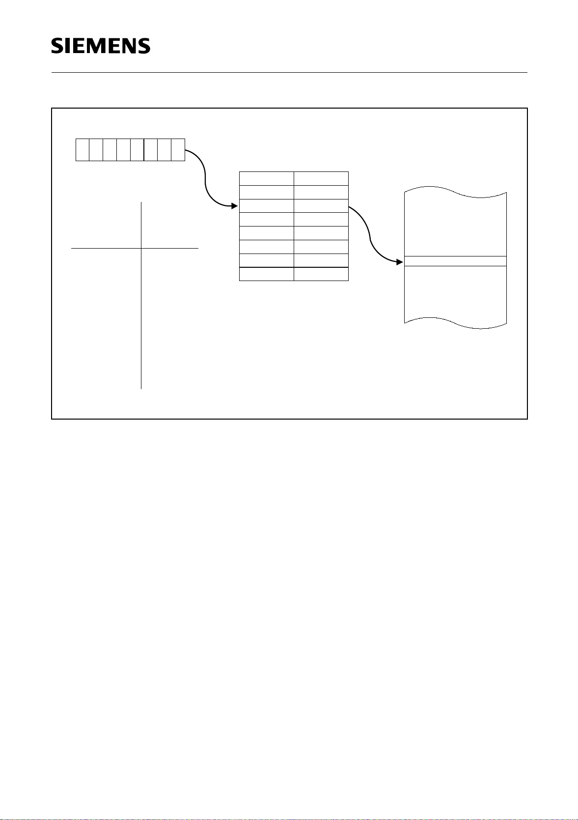
External Bus Interface
C515C
Datapointer
DPTR 0000
.0.1.2
DPTR7
DPTR0
DPH(83 ) DPL(82 )
HH
DPSEL(92 )
DPSEL Selected
.2 .1 .0
0 0 1 DPTR 1
0 1 0 DPTR 2
0 1 1 DPTR 3
1 0 0 DPTR 4
1 0 1 DPTR 5
1 1 0 DPTR 6
1 1 1 DPTR 7
H
-----
Figure 4-3
Accessing of External Data Memory via Multiple Datapointers
External Data Memory
MCD00779
4.6.3 Advantages of Multiple Datapointers
Using the above addressing mechanism for external data memory results in less code and faster
execution of external accesses. Whenever the contents of the datapointer must be altered between
two or more 16-bit addresses, one single instruction, which selects a new datapointer, does this job.
lf the program uses just one datapointer, then it has to save the old value (with two 8-bit instructions)
and load the new address, byte by byte. This not only takes more time, it also requires additional
space in the internal RAM.
4.6.4 Application Example and Performance Analysis
The following example shall demonstrate the involvement of multiple data pointers in a table
transfer from the code memory to external data memory.
Start address of ROM source table: 1FFF
Start address of table in external RAM: 2FA0
H
H
Semiconductor Group 4-7 1997-10-01
Page 51

External Bus Interface
C515C
Example 1 : Using only One Datapointer (Code for an C501)
Initialization Routine
MOV LOW(SRC_PTR), #0FFH ;Initialize shadow_variables with source_pointer
MOV HIGH(SRC_PTR), #1FH
MOV LOW(DES_PTR), #0A0H ;Initialize shadow_variables with destination_pointer
MOV HIGH(DES_PTR), #2FH
Table Look-up Routine under Real Time Conditions
; Number of cycles
PUSH DPL ;Save old datapointer 2
PUSH DPH ; 2
MOV DPL, LOW(SRC_PTR) ;Load Source Pointer 2
MOV DPH, HIGH(SRC_PTR) ; 2
;INC DPTR Increment and check for end of table (execution time
;CJNE … not relevant for this consideration) –
MOVC A,@DPTR ;Fetch source data byte from ROM table 2
MOV LOW(SRC_PTR), DPL ;Save source_pointer and 2
MOV HIGH(SRC_PTR), DPH ;load destination_pointer 2
MOV DPL, LOW(DES_PTR) ; 2
MOV DPH, HIGH(DES_PTR) ; 2
INC DPTR ;Increment destination_pointer
;(ex. time not relevant) –
MOVX @DPTR, A ;Transfer byte to destination address 2
MOV LOW(DES_PTR), DPL ;Save destination_pointer 2
MOV HIGH(DES_PTR),DPH ; 2
POP DPH ;Restore old datapointer 2
POP DPL ; 2
; Total execution time (machine cycles) : 28
Semiconductor Group 4-8 1997-10-01
Page 52

External Bus Interface
C515C
Example 2 : Using Two Datapointers (Code for an C515C)
Initialization Routine
MOV DPSEL, #06H ;Initialize DPTR6 with source pointer
MOV DPTR, #1FFFH
MOV DPSEL, #07H ;Initialize DPTR7 with destination pointer
MOV DPTR, #2FA0H
Table Look-up Routine under Real Time Conditions
; Number of cycles
PUSH DPSEL ;Save old source pointer 2
MOV DPSEL, #06H ;Load source pointer 2
;INC DPTR Increment and check for end of table (execution time
;CJNE … not relevant for this consideration) –
MOVC A,@DPTR ;Fetch source data byte from ROM table 2
MOV DPSEL, #07H ;Save source_pointer and
;load destination_pointer 2
MOVX @DPTR, A ;Transfer byte to destination address 2
POP DPSEL ;Save destination pointer and
;restore old datapointer 2
; Total execution time (machine cycles) : 12
The above example shows that utilization of the C515C’s multiple datapointers can make external
bus accesses two times as fast as with a standard 8051 or 8051 derivative. Here, four data variables
in the internal RAM and two additional stack bytes were spared, too. This means for some
applications where all eight datapointers are employed that an C515C program has up to 24 byte
(16 variables and 8 stack bytes) of the internal RAM free for other use.
Semiconductor Group 4-9 1997-10-01
Page 53

External Bus Interface
C515C
4.7 ROM/OTP Protection for the C515C-8R / C515C-8E
The C515C-8R ROM version allows to protect the contents of the internal ROM against read out by
non authorized people. The type of ROM protection (protected or unprotected) is fixed with the
ROM mask. Therefore, the customer of a C515C-8R ROM version has to define whether ROM
protection has to be selected or not.
The C515C-8E OTP version allows also program memory protection in several levels (see
chapter 10.6). The program memory protection for the C515C-8E can be activated after
programming of the device.
The C515C-8R devices, which operate from internal ROM, are always checked for correct ROM
contents during production test. Therefore, unprotected and also protected ROMs must provide a
procedure to verify the ROM contents. In ROM verification mode 1, which is used to verify
unprotected ROMs, a ROM address is applied externally to the C515C-8R and the ROM data byte
is output at port 0. ROM verification mode 2, which is used to verify ROM and OTP (in protection
level 1) protected devices, operates different : ROM addresses are generated internally and the
expected data bytes must be applied externally to the device (by the manufacturer or by the
customer) and are compared internally with the data bytes from the ROM. After 16 byte verify
operations the state of the P3.5 pin shows whether the last 16 bytes have been verified correctly.
This mechanism provides a very high security of ROM protection. Only the owner of the ROM code
and the manufacturer who know the contents of the ROM can read out and verify it with less effort.
4.7.1 Unprotected ROM Mode
If the ROM is unprotected, the ROM verification mode 1 as shown in figure 4-4 is used to read out
the contents of the ROM. The AC timing characteristics of the ROM verification mode is shown in
the AC specifications (chapter 11).
Figure 4-4
ROM Verification Mode 1
ROM verification mode 1 is selected if the inputs PSEN
specified logic level. Then the 16-bit address of the internal ROM byte to be read is applied to the
port 1 and port 2 lines. After a delay time, port 0 outputs the content of the addressed ROM cell. In
ROM verification mode 1, the C515C-8R must be provided with a system clock at the XTAL pins and
pullup resistors on the port 0 lines.
Semiconductor Group 4-10 1997-10-01
, ALE, EA, and RESET are put to the
Page 54
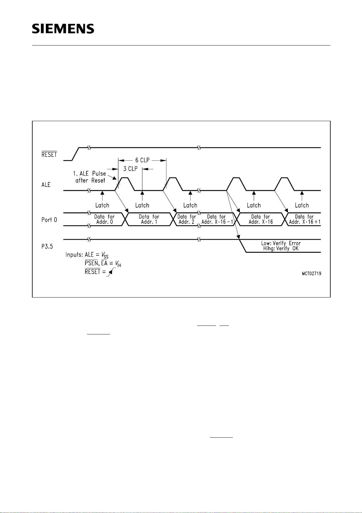
External Bus Interface
C515C
4.7.2 Protected ROM/OTP Mode
If the C515C-8R ROM is protected by mask (or C515C-8E in protection level 1), the ROM/OTP
verification mode 2 as shown in figure 4-5 is used to verify the content of the ROM/OTP. The
detailed timing characteristics of the ROM verification mode is shown in the AC specifications
(chapter 11).
Figure 4-5
ROM/OTP Verification Mode 2
ROM/OTP verification mode 2 is selected if the inputs PSEN, EA, and ALE are put to the specified
logic levels. With RESET going inactive, the ROM/OTP verification mode 2 sequence is started.
The C515C outputs an ALE signal with a period of 3 CLP and expects data bytes at port 0. The data
bytes at port 0 are assigned to the ROM addresses in the following way :
1. Data Byte = content of internal ROM/OTP address 0000
2. Data Byte = content of internal ROM/OTP address 0001
3. Data Byte = content of internal ROM/OTP address 0002
:
16. Data Byte= content of internal ROM/OTP address 000FH
:
The C515C does not output any address information during the ROM/OTP verification mode 2. The
first data byte to be verified is always the byte which is assigned to the internal ROM address 0000
and must be put onto the data bus with the rising edge of RESET
the ROM/OTP address pointer is internally incremented and the expected data byte for the next
ROM/OTP address must be delivered externally.
H
H
H
H
. With each following ALE pulse
Semiconductor Group 4-11 1997-10-01
Page 55
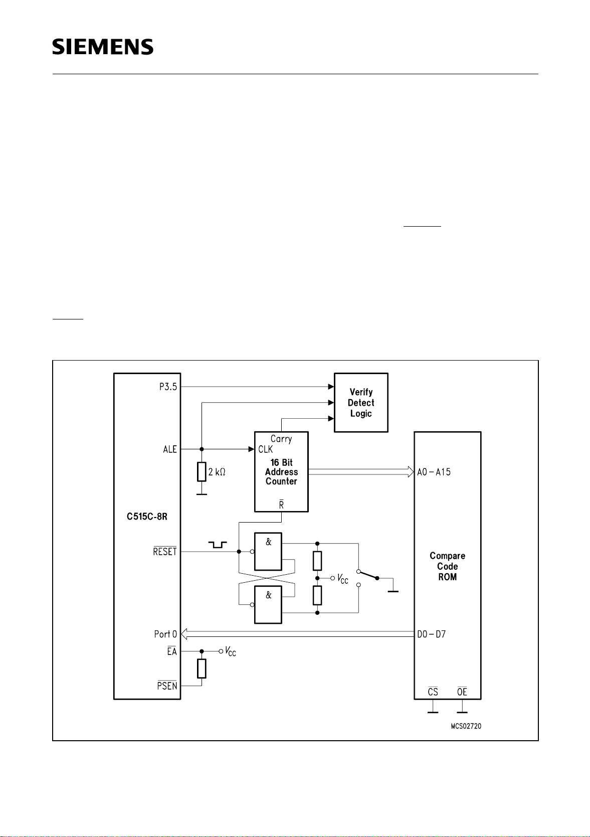
External Bus Interface
C515C
Between two ALE pulses the data at port 0 is latched (at 3 CLP after ALE rising edge) and compared
internally with the ROM/OTP content of the actual address. If an verify error is detected, the error
condition is stored internally. After each 16th data byte the cumulated verify result (pass or fail) of
the last 16 verify operations is output at P3.5. If P3.5 has been set low (verify error detected), it will
stay at low level even if the following ROM verification sequence does not detect further verify
errors. In ROM/OTP verification mode 2, the C515C must be provided with a system clock at the
XTAL pins.
Figure 4-6 shows an application example of a external circuitry which allows to verify a protected
ROM/OTP inside the C515C in ROM/OTP verification mode 2. With RESET going inactive, the
C515C starts the ROM/OTP verify sequence. Its ALE is clocking an 16-bit address counter. This
counter generates the addresses for an external EPROM which is programmed with the contents of
the internal (protected) ROM/OTP. The verify detect logic typically displays the pass/fail information
of the verify operation. P3.5 can be latched with the falling edge of ALE.
When the last byte of the internal ROM/OTP has been handled, the C515C starts generating a
PSEN signal. This signal or the CY signal of the address counter indicate to the verify detect logic
the end of the internal ROM/OTP verification.
Figure 4-6
ROM Verification Mode 2 - External Circuitry Example
Semiconductor Group 4-12 1997-10-01
Page 56

Reset / System Clock
C515C
5 Reset and System Clock Operation
5.1 Hardware Reset Operation
The hardware reset function incorporated in the C515C allows for an easy automatic start-up at a
minimum of additional hardware and forces the controller to a predefined default state. The
hardware reset function can also be used during normal operation in order to restart the device. This
is particularly done when the power-down mode is to be terminated.
Additionally to the hardware reset, which is applied externally to the C515C, there are two internal
reset sources, the watchdog timer and the oscillator watchdog. The chapter at hand only deals with
the external hardware reset.
The reset input is an active low input. An internal Schmitt trigger is used at the input for noise
rejection. Since the reset is synchronized internally, the RESET pin must be held low for at least two
machine cycle (12 oscillator periods) while the oscillator is running. With the oscillator running the
internal reset is executed during the second machine cycle and is repeated every cycle until RESET
goes high again.
During reset, pins ALE and PSEN are configured as inputs and should not be stimulated externally.
An external stimulation at these lines during reset activates several test modes which are reserved
for test purposes. This in turn may cause unpredictable output operations at several port pins.
A pullup resistor is internally connected to VCC to allow a power-up reset with an external capacitor
only. An automatic reset can be obtained when VCC is applied by connecting the RESET pin to V
via a capacitor (figure 5-1 a) and c)). After VCC has been turned on, the capacitor must hold the
voltage level at the reset pin for a specific time to effect a complete reset.
SS
Semiconductor Group 5-1 1997-10-01
Page 57
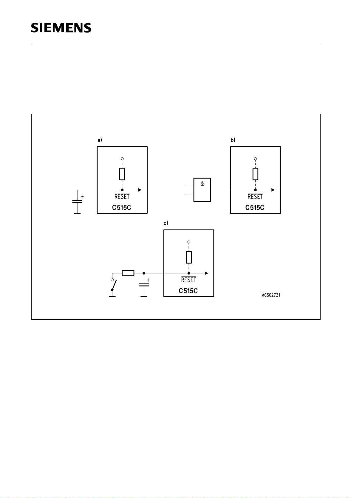
Reset / System Clock
C515C
The time required for a reset operation is the oscillator start-up time plus 2 machine cycles, which,
under normal conditions, must be at least 10 - 20 ms for a crystal oscillator. This requirement is
typically met using a capacitor of 4.7 to 10 µF. The same considerations apply if the reset signal is
generated externally (figure 5-1 b). In each case it must be assured that the oscillator has started
up properly and that at least two machine cycles have passed before the reset signal goes inactive.
Figure 5-1
Reset Circuitries
A correct reset leaves the processor in a defined state. The program execution starts at location
0000H. After reset is internally accomplished the port latches are set to FFH. This leaves port 0
floating, since it is an open drain port when not used as data/address bus. All other I/O port lines
(ports 1 to 5 and 7) output a one (1). Port 6 is an input-only port. It has no internal latch and therefore
the contents of the special function registers P6 depend on the levels applied to port 6.
The content of the internal RAM and XRAM of the C515C is not affected by a reset. After power-up
the content is undefined, while it remains unchanged during a reset if the power supply is not turned
off.
Semiconductor Group 5-2 1997-10-01
Page 58

Reset / System Clock
C515C
5.2 Hardware Reset Timing
This section describes the timing of the hardware reset signal.
The input pin RESET is sampled once during each machine cycle. This happens in state 5 phase 2.
Thus, the external reset signal is synchronized to the internal CPU timing. When the reset is found
active (low level) the internal reset procedure is started. It needs two machine cycles to put the
complete device to its correct reset state, i.e. all special function registers contain their default
values, the port latches contain 1's etc. Note that this reset procedure is also performed if there is
no clock available at the device. This is done by the oscillator watchdog, which provides an auxiliary
clock for performing a perfect reset without clock at the XTAL1 and XTAL2 pins. The RESET signal
must be active for at least one machine cycle. After this time the C515C remains in its reset state
as long as the signal is active. When the reset signal goes inactive this transition is recognized in the
following state 5 phase 2 of the machine cycle. Then the processor starts its address output (when
configured for external ROM) in the following state 5 phase 1. One phase later (state 5 phase 2) the
first falling edge at pin ALE occurs.
Figure 5-2 shows this timing for a configuration with EA = 0 (external program memory). Thus,
between the release of the RESET signal and the first falling edge at ALE there is a time period of
at least one machine cycle but less than two machine cycles.
Figure 5-2
CPU Timing after Reset
Semiconductor Group 5-3 1997-10-01
Page 59

Reset / System Clock
C515C
5.3 Fast Internal Reset after Power-On
The C515C uses the oscillator watchdog unit (see also chapter 8) for a fast internal reset procedure
after power-on. Figure 5-3 shows the power-on sequence under control of the oscillator watchdog.
Normally the devices of the 8051 family enter their default reset state not before the on-chip
oscillator starts. The reason is that the external reset signal must be internally synchronized and
processed in order to bring the device into the correct reset state. Especially if a crystal is used the
start up time of the oscillator is relatively long (max. 10 ms). During this time period the pins have
an undefined state which could have severe effects especially to actuators connected to port pins.
In the C515C the oscillator watchdog unit avoids this situation. In this case, after power-on the
oscillator watchdog's RC oscillator starts working within a very short start-up time (typ. less than
2 microseconds). In the following the watchdog circuitry detects a failure condition for the on-chip
oscillator because this has not yet started (a failure is always recognized if the watchdog's RC
oscillator runs faster than the on-chip oscillator). As long as this condition is detected the watchdog
uses the RC oscillator output as clock source for the chip rather than the on-chip oscillator's output.
This allows correct resetting of the part and brings also all ports to the defined state (see figure 5-3).
Under worst case conditions (fast VCC rise time - e.g. 1µs, measured from VCC = 4.25 V up to stable
port condition), the delay between power-on and the correct port reset state is :
– Typ.: 18 µs
– Max.: 34 µs
The RC oscillator will already run at a VCC below 4.25 V (lower specification limit). Therefore, at
slower VCC rise times the delay time will be less than the two values given above.
After the on-chip oscillator finally has started, the oscillator watchdog detects the correct function;
then the watchdog still holds the reset active for a time period of max. 768 cycles of the RC oscillator
clock in order to allow the oscillation of the on-chip oscillator to stabilize (figure 5-3, II).
Subsequently, the clock is supplied by the on-chip oscillator and the oscillator watchdog's reset
request is released (figure 5-3, III). However, an externally applied reset still remains active
(figure 5-3, IV) and the device does not start program execution (figure 5-3, V) before the external
reset is also released.
Although the oscillator watchdog provides a fast internal reset it is additionally necessary to apply
the external reset signal when powering up. The reasons are as follows:
– Termination of Hardware Power-Down Mode (a HWPD
– Termination of the Software Power Down Mode
– Reset of the status flag OWDS that is set by the oscillator watchdog during the power up
sequence.
signal is overriden by reset)
Using a crystal for clock generation, the external reset signal must be hold active at least until the
on-chip oscillator has started (max.10 ms) and the internal watchdog reset phase is completed
(after phase III in figure 5-3). When an external clock generator is used, phase II is very short.
Therefore, an external reset time of typically 1 ms is sufficient in most applications.
Generally, for reset time generation at power-on an external capacitor can be applied to the RESET
pin.
Semiconductor Group 5-4 1997-10-01
Page 60

Reset / System Clock
C515C
MCD02722
execution
program
Start of
Port remains
in reset
ext. reset
because of
signal
ResetUndef.Ports
final reset
sequence by
starts;
On-chip oscillator
Reset at Ports
Clock from RC-Oscillator,
µ
I II III IV V
Port
18 s
undef.
Power On;
typ.
768 Cycles
oscillator WD;
max.
µ
34 s
max.
Oscillator
On-Chip
RC
Oscillator
CC
V
RESET
Phase
Figure 5-3
Power-On Reset of the C515C
Semiconductor Group 5-5 1997-10-01
Page 61

Reset / System Clock
C515C
5.4 Oscillator and Clock Circuit
XTAL1 and XTAL2 are the output and input of a single-stage on-chip inverter which can be
configured with off-chip components as a Pierce oscillator. The oscillator, in any case, drives the
internal clock generator. The clock generator provides the internal clock signals to the chip. These
signals define the internal phases, states and machine cycles.
Figure 5-4 shows the recommended oscillator circuit.
Figure 5-4
Recommended Oscillator Circuit
In this application the on-chip oscillator is used as a crystal-controlled, positive-reactance oscillator
(a more detailed schematic is given in figure 5-5). lt is operated in its fundamental response mode
as an inductive reactor in parallel resonance with a capacitor external to the chip. The crystal
specifications and capacitances are non-critical. In this circuit 20 pF can be used as single
capacitance at any frequency together with a good quality crystal. A ceramic resonator can be used
in place of the crystal in cost-critical applications. lt a ceramic resonator is used, C1 and C2 are
normally selected to be of somewhat higher values, typically 47 pF. We recommend consulting the
manufacturer of the ceramic resonator for value specifications of these capacitors.
Semiconductor Group 5-6 1997-10-01
Page 62
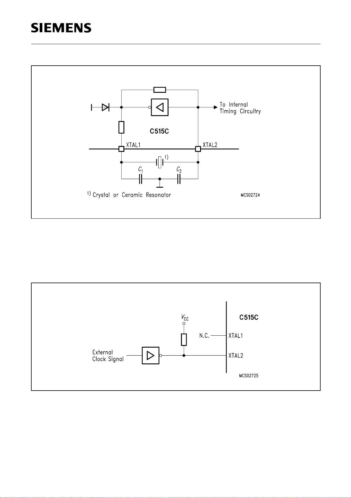
Reset / System Clock
C515C
Figure 5-5
On-Chip Oscillator Circuitry
To drive the C515C with an external clock source, the external clock signal has to be applied to
XTAL2, as shown in figure 5-6. XTAL1 has to be left unconnected. A pullup resistor is suggested
(to increase the noise margin), but is optional if VOH of the driving gate corresponds to the V
IH2
specification of XTAL2.
Figure 5-6
External Clock Source
Semiconductor Group 5-7 1997-10-01
Page 63

Reset / System Clock
C515C
5.5 System Clock Output
For peripheral devices requiring a system clock, the C515C provides a clock output signal derived
from the oscillator frequency as an alternate output function on pin P1.6/CLKOUT. lf bit CLK is set
(bit 6 of special function register ADCON0), a clock signal with 1/6 of the oscillator frequency is
gated to pin P1.6/CLKOUT. To use this function the port pin must be programmed to a one (1),
which is also the default after reset.
Special Function Register ADCON0 (Address D8H) Reset Value : 00
H
LSB
D8
H
ADCON0
MSB
Bit No. DF
D8
H
Bit Function
CLK Clockout enable bit
The system clock is high during S3P1 and S3P2 of every machine cycle and low during all other
states. Thus, the duty cycle of the clock signal is 1:6. Associated with a MOVX instruction the
system clock coincides with the last state (S3) in which a RD or WR signal is active. A timing
diagram of the system clock output is shown in figure 5-7.
Note : During slow-down operation the frequency of the CLKOUT signal is divided by 32.
BD CLK ADEX BSY
The shaded bits are not used in controlling the clock output function.
DE
H
When set, pin P1.6/CLKOUT outputs the system clock which is 1/6 of the
oscillator frequency.
H
DD
H
DC
DB
H
ADM MX2 MX1 MX0
H
DA
H
D9
H
Semiconductor Group 5-8 1997-10-01
Page 64
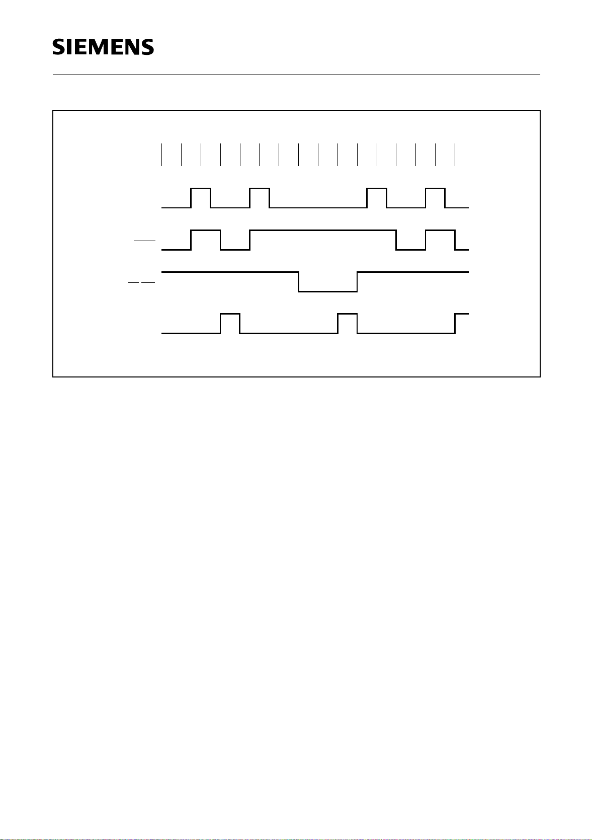
Reset / System Clock
C515C
S6 S1 S2 S3 S4 S5 S6 S1 S2 S3 S4 S5 S6 S1 S2
ALE
PSEN
RD,WR
CLKOUT
Figure 5-7
Timing Diagram - System Clock Output
MCT01858
Semiconductor Group 5-9 1997-10-01
Page 65

On-Chip Peripheral Components
C515C
6 On-Chip Peripheral Components
This chapter gives detailed information about all on-chip peripherals of the C515C except for the
integrated interrupt controller, which is described separately in chapter 7.
6.1 Parallel I/O
6.1.1 Port Structures
Digital I/O Ports
The C515C allows for digital I/O on 49 lines grouped into 6 bidirectional 8-bit ports and one 1-bit
port. Each port bit consists of a latch, an output driver and an input buffer. Read and write accesses
to the I/O ports P0 through P7 are performed via their corresponding special function registers P0
to P7. The port structure of port 5 of the C515C is especially designed to operate either as a quasibidirectional port structure, compatible to the standard 8051-Family, or as a genuine bidirectional
port structure. This port operating mode can be selected by software (setting or clearing the bit
PMOD in the SFR SYSCON).
The output drivers of port 0 and 2 and the input buffers of port 0 are also used for accessing external
memory. In this application, port 0 outputs the low byte of the external memory address, timemultiplexed with the byte being written or read. Port 2 outputs the high byte of the external memory
address when the address is 16 bits wide. Otherwise, the port 2 pins continue emitting the P2 SFR
contents.
Analog Input Ports
Ports 6 is available as input port only and provides two functions. When used as digital inputs, the
corresponding SFR P6 contains the digital value applied to the port 6 lines. When used for analog
inputs the desired analog channel is selected by a three-bit field in SFR ADCON0 or SFR ADCON1.
Of course, it makes no sense to output a value to these input-only ports by writing to the SFR P6.
This will have no effect.
lf a digital value is to be read, the voltage levels are to be held within the input voltage specifications
(VIL/VIH). Since P6 is not bit-addressable, all input lines of P6 are read at the same time by byte
instructions.
Nevertheless, it is possible to use port 6 simultaneously for analog and digital input. However, care
must be taken that all bits of P6 that have an undetermined value caused by their analog function
are masked.
In order to guarantee a high-quality A/D conversion, digital input lines of port 6 should not toggle
while a neighbouring port pin is executing an A/D conversion. This could produce crosstalk to the
analog signal.
Semiconductor Group 6-1 1997-10-01
Page 66
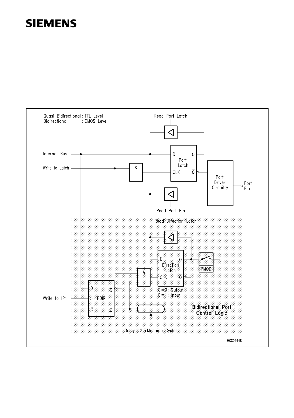
On-Chip Peripheral Components
C515C
Figure 6-1 shows a functional diagram of a typical bit latch and I/O buffer, which is the core of each
of the 7 digital I/O-ports. The bit latch (one bit in the port’s SFR) is represented as a type-D flip-flop,
which will clock in a value from the internal bus in response to a "write-to-latch" signal from the CPU.
The Q output of the flip-flop is placed on the internal bus in response to a "read-latch" signal from
the CPU. The level of the port pin self is placed on the internal bus in response to a "read-pin" signal
from the CPU. Some instructions that read from a port activate the "read-port-latch" signal, while
others activate the "read-port-pin" signal.
Figure 6-1
Basic Structure of a Port Circuitry
The shaded area in figure 6-1 shows the control logic of the C515C port 5 circuitry, which has been
added to the functionality of the standard 8051 digital I/O port structure. This control logic is used
to provide the additional bidirectional port 5 structure with CMOS voltage levels.
Semiconductor Group 6-2 1997-10-01
Page 67
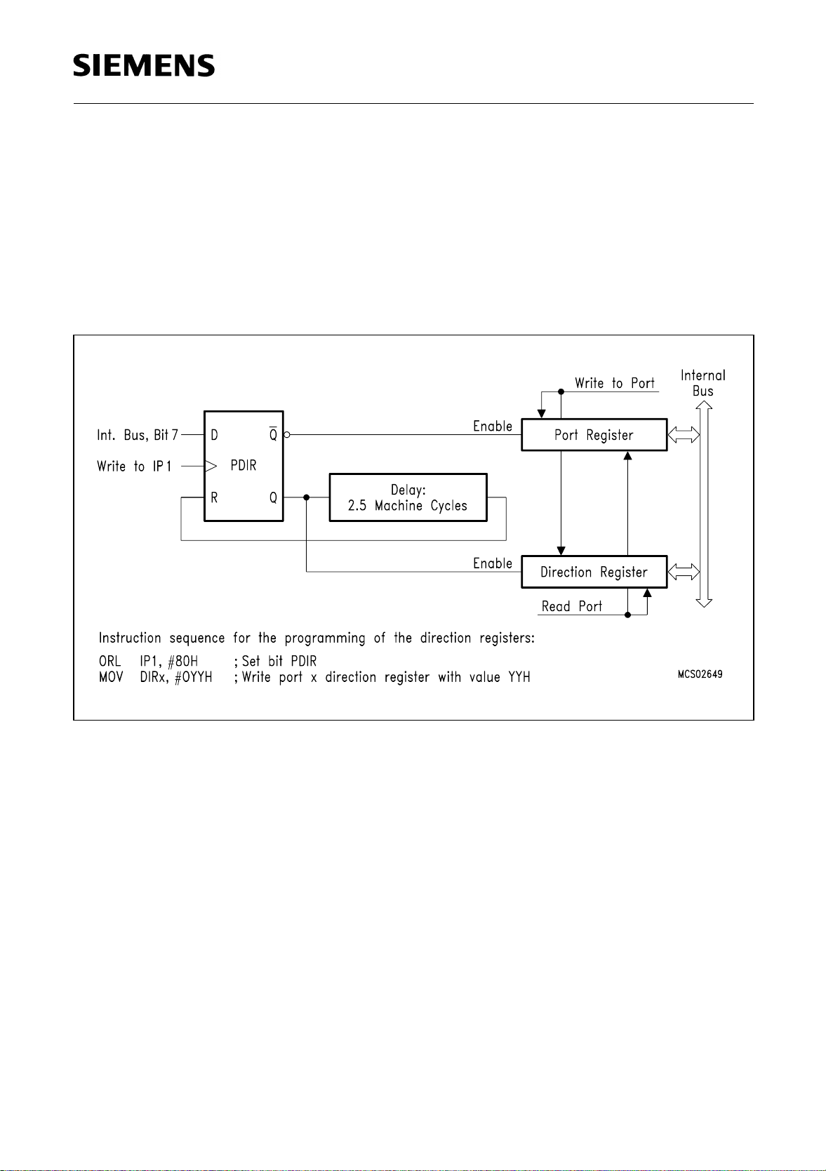
On-Chip Peripheral Components
C515C
6.1.1.1 Port Structure Selection
After a reset operation, the quasi-bidirectional 8051-compatible port structure is selected for all
digital I/O ports of the C515C. For selection of the bidirectional (CMOS) port 5 structure the bit
PMOD of SFR SYSCON must be set. Because each port 5 pin can be programmed as an input or
an output, additionally, after the selection of the bidirectional mode, the direction register DIR5 of
port 5 must be written . This direction register is mapped to the port 5 register. This means, the port
register address is equal to its direction register address. Figure 6-2 illustrates the port- and
direction register configuration of port 5.
Figure 6-2
Port 5 Register, Direction Register
For the access the direction register a double instruction sequence must be executed. The first
instruction has to set bit PDIR in SFR IP1. Thereafter, a second instruction can read or write the
direction registers. PDIR will automatically be cleared after the second machine cycle (S2P2) after
having been set. For this time, the access to the direction register is enabled and the register can
be read or written. Further, the double instruction sequence as shown in figure 6-2, cannot be
interrupted by an interrupt,
When the bidirectional port structure is activated (PMOD=1) after a reset, the ports are defined as
inputs (direction registers default values after reset are set to FFH).
With PMOD = 0 (quasi-bidirectional port structure selected), any access to the direction registers
has no effect on the port driver circuitries.
Semiconductor Group 6-3 1997-10-01
Page 68
On-Chip Peripheral Components
C515C
Special Function Register SYSCON (Address B1H) Reset Value C515C-8R : X010XX01
Reset Value C515C-8E : X010X001
Special Function Register IP1 (Address B9H) Reset Value : 0X000000
MSB
Bit No. 76543210
B1
H
Bit No. 76543210
B9
H
The shaded bits are not used for port selection.
Bit Function
PMOD Port 5 mode selection
PDIR Direction register enable
– PMOD EALE RMAP
PDIR – .5 .4
PMOD = 0 : Quasi-bidirectional port structure of port 5 is selected (reset value)
PMOD = 1 : Bidirectional port structure of port 5 is selected.
PDIR = 0 : Port 5 register access is enabled (reset value)
PDIR = 1 : Direction register is enabled.
PDIR will automatically be cleared after the second machine cycle (S2P2) after
having been set.
– CSWO XMAP1 XMAP0
.3 .2 .1 .0
LSB
SYSCON
IP1
B
B
B
Direction Register DIR5 (Address F8H) Reset Value : FF
MSB
Bit No. 76543210
F8
H
Bit Function
DIR5.7-0 Port driver circuitry, input/output selection
.7 .6 .5 .4
Bit = 0 : Port line is in output mode
Bit = 1 : Port line is in input mode (reset value).
This register can only be read and written by software when bit PDIR (IP1) was set
one instruction before.
.3 .2 .1 .0
LSB
DIR5
H
Semiconductor Group 6-4 1997-10-01
Page 69
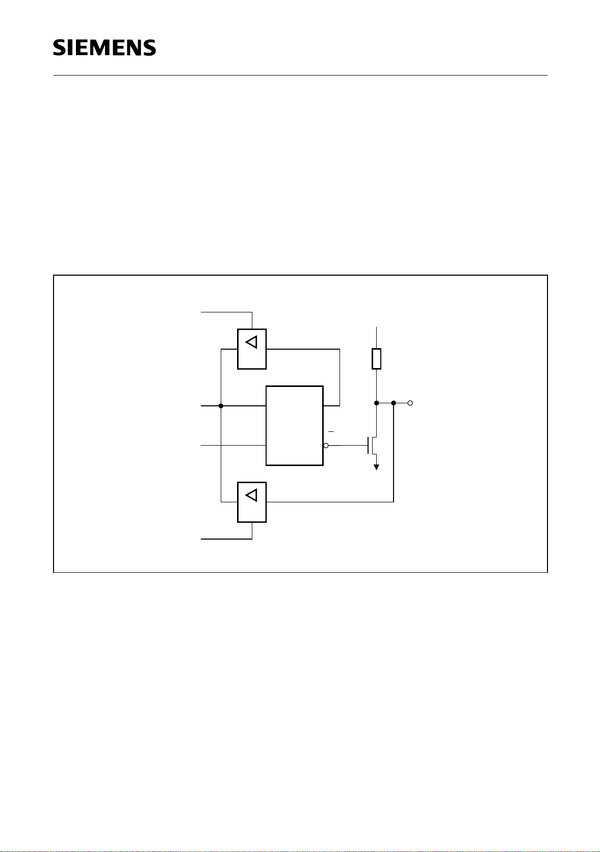
On-Chip Peripheral Components
C515C
6.1.1.2 Quasi-Bidirectional Port Structure
6.1.1.2.1 Basic Port Circuirty of Port 1 to 5 and 7
The basic quasi-bidirectional port structure as shown in the upper part of the schematics of
figure 6-3 provides a port driver circuit which is build up by an internal pullup FET as shown in
figure 6-3. Each I/O line can be used independently as an input or output. To be used as an input,
the port bit stored in the bit latch must contain a one (1) (that means for figure 6-3, Q=0), which
turns off the output driver FET n1. Then, for ports 1 to 5 and 7, the pin is pulled high by the internal
pullups, but can be pulled low by an external source. When externally pulled low the port pins
source current (IIL or ITL). For this reason these ports are sometimes called "quasi-bidirectional".
Read
Latch
Int. Bus
Write
to
Latch
Read
Pin
D
Bit
Latch
CLK
Figure 6-3
Basic Output Driver Circuit of Ports 1 to 5 and 7
V
CC
Internal
Pull Up
Arrangement
Q
Q
n1
MCS01823
Pin
Semiconductor Group 6-5 1997-10-01
Page 70
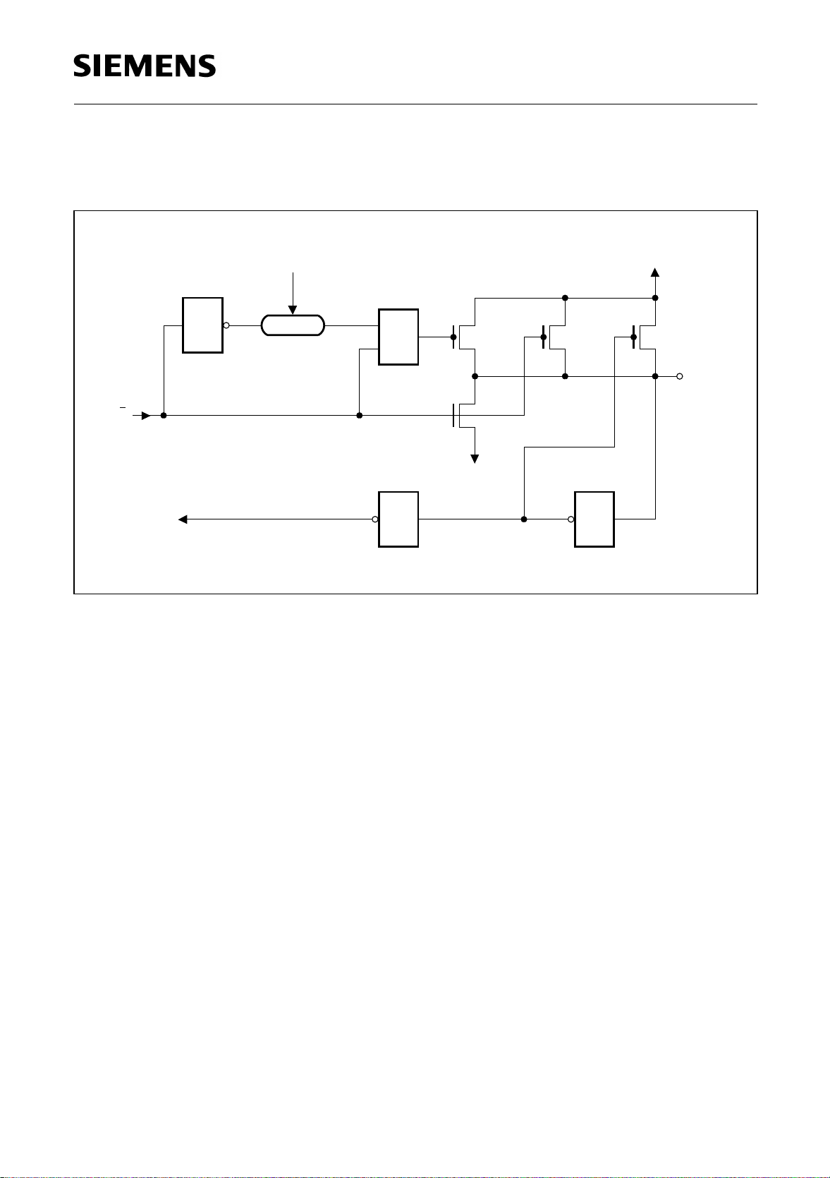
On-Chip Peripheral Components
C515C
In fact, the pullups mentioned before and included in figure 6-3 are pullup arrangements as shown
in figure 6-4. One n-channel pulldown FET and three pullup FETs are used:
V
CC
Port
Pin
MCS03230
Q
Input Data
(Read Pin)
=1
Delay = 1 State
_
<
1
p1 p2 p3
n1
V
SS
=1=1
Figure 6-4
Output Driver Circuit of Ports 1 to 5 and 7
– The pulldown FET n1 is of n-channel type. It is a very strong driver transistor which is capable
of sinking high currents (IOL); it is only activated if a "0" is programmed to the port pin. A short
circuit to VCC must be avoided if the transistor is turned on, since the high current might destroy
the FET. This also means that no ”0“ must be programmed into the latch of a pin that is used
as input.
– The pullup FET p1 is of p-channel type. It is activated for one state (S1) if a 0-to-1 transition
is programmed to the port pin, i.e. a "1" is programmed to the port latch which contained a "0".
The extra pullup can drive a similar current as the pulldown FET n1. This provides a fast
transition of the logic levels at the pin.
– The pullup FET p2 is of p-channel type. It is always activated when a "1" is in the port latch,
thus providing the logic high output level. This pullup FET sources a much lower current than
p1; therefore the pin may also be tied to ground, e.g. when used as input with logic low input
level.
– The pullup FET p3 is of p-channel type. It is only activated if the voltage at the port pin is
higher than approximately 1.0 to 1.5 V. This provides an additional pullup current if a logic
high level shall be output at the pin (and the voltage is not forced lower than approximately
1.0 to 1.5 V). However, this transistor is turned off if the pin is driven to a logic low level, e.g
when used as input. In this configuration only the weak pullup FET p2 is active, which sources
the current IIL . If, in addition, the pullup FET p3 is activated, a higher current can be sourced
(ITL). Thus, an additional power consumption can be avoided if port pins are used as inputs
with a low level applied. However, the driving capability is stronger if a logic high level is
output.
Semiconductor Group 6-6 1997-10-01
Page 71

On-Chip Peripheral Components
C515C
The described activating and deactivating of the four different transistors results in four states which
can be :
– input low state (IL), p2 active only
– input high state (IH) = steady output high state (SOH), p2 and p3 active
– forced output high state (FOH), p1, p2 and p3 active
– output low state (OL), n1 active
If a pin is used as input and a low level is applied, it will be in IL state, if a high level is applied, it
will switch to IH state. If the latch is loaded with "0", the pin will be in OL state. If the latch holds a
"0" and is loaded with "1", the pin will enter FOH state for two cycles and then switch to SOH state.
If the latch holds a "1" and is reloaded with a "1" no state change will occur.
At the beginning of power-on reset the pins will be in IL state (latch is set to "1", voltage level on
pin is below of the trip point of p3). Depending on the voltage level and load applied to the pin, it will
remain in this state or will switch to IH (=SOH) state.
If it is is used as output, the weak pull-up p2 will pull the voltage level at the pin above p3’s trip point
after some time and p3 will turn on and provide a strong "1". Note, however, that if the load exceeds
the drive capability of p2 (IIL), the pin might remain in the IL state and provide a week "1" until the
first 0-to-1 transition on the latch occurs. Until this the output level might stay below the trip point of
the external circuitry.
The same is true if a pin is used as bidirectional line and the external circuitry is switched from
output to input when the pin is held at "0" and the load then exceeds the p2 drive capabilities.
If the load exceeds IIL the pin can be forced to “1“ by writing a “0“ followed by a “1“ to the port pin..
Note : The port 4 pins P4.1 to P4.4 are used by the SSC interface as alternate functions pins. The
detailed port structure of these four port 4 pins is described in section 6.1.1.2.4
Semiconductor Group 6-7 1997-10-01
Page 72
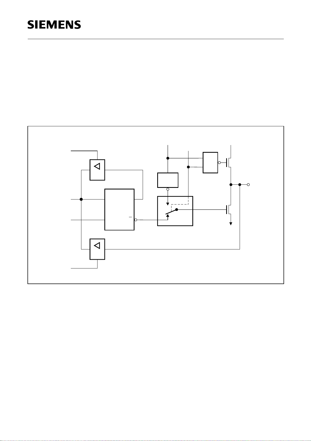
On-Chip Peripheral Components
C515C
6.1.1.2.2 Port 0 Circuitry
Port 0, in contrast to ports 1 to 5 and 7, is considered as "true" bidirectional, because the port 0 pins
float when configured as inputs. Thus, this port differs in not having internal pullups. The pullup FET
in the P0 output driver (see figure 6-5) is used only when the port is emitting 1 s during the external
memory accesses. Otherwise, the pullup is always off. Consequently, P0 lines that are used as
output port lines are open drain lines. Writing a "1" to the port latch leaves both output FETs off and
the pin floats. In that condition it can be used as high-impedance input. If port 0 is configured as
general I/O port and has to emit logic high-level (1), external pullups are required.
Read
Latch
Bus
Int.
Write to
Latch
Read
Pin
Figure 6-5
Port 0 Circuitry
D
CLK
Bit
Latch
Addr./Data
Control
&
=1
Q
Q
MUX
V
CC
MCS02434
Port
Pin
Semiconductor Group 6-8 1997-10-01
Page 73

On-Chip Peripheral Components
C515C
6.1.1.2.3 Port 0 and Port 2 used as Address/Data Bus
As shown in figure 6-5 and below in figure 6-6, the output drivers of ports 0 and 2 can be switched
to an internal address or address/data bus for use in external memory accesses. In this application
they cannot be used as general purpose I/O, even if not all address lines are used externally. The
switching is done by an internal control signal dependent on the input level at the EA pin and/or the
contents of the program counter. If the ports are configured as an address/data bus, the port latches
are disconnected from the driver circuit. During this time, the P2 SFR remains unchanged while the
P0 SFR has 1’s written to it. Being an address/data bus, port 0 uses a pullup FET as shown in
figure 6-5. When a 16-bit address is used, port 2 uses the additional strong pullups p1 to emit 1’s
for the entire external memory cycle instead of the weak ones (p2 and p3) used during normal port
activity.
Read
Latch
Addr.
Control
V
CC
Int. Bus
Write to
Latch
Read
Pin
Figure 6-6
Port 2 Circuitry
D
CLK
Bit
Latch
Internal
Pull Up
Arrangement
Q
MUX
Q
=1
MCS02123
Port
Pin
Semiconductor Group 6-9 1997-10-01
Page 74

On-Chip Peripheral Components
C515C
6.1.1.2.4 SSC Port Pins of Port 4
The port pins of the SSC interface are located as alternate functions at four lines of port 4 :
– P4.1/SCLK : when used as SSC clock output, pin becomes a true push-pull output
– P4.2/SRI : when used as SSC receiver input, pin becomes an input without pullups.
– P4.3/STO : when used as SSC transmitter output, pin becomes a true push-pull output with
tristate capability
– P4.4/SLS : when used as SSC slave select input, pin directly controls the tristate condition
of P4.3
The modified port 4 structure for the two SSC outputs SCLK and STO is illustrated in figure 6-7.
This figure can be compared with figure 6-4.
Figure 6-7
Driver Circuit of Port 4 Pins P4.1and P4.3 (when used for SLCK and STO)
Pin Control for P4.1/SCLK
When the SSC is disabled, both control lines “Enable Push-pull“ and “Tristate“ will be inactive, the
pin behaves like a standard IO pin. In master mode with SSC enabled, “Enable Push-pull“ will be
active and “Tristate“ will be inactive. In slave mode with SSC enabled, “Enable Push-pull“ will be
inactive and “Tristate“ will be active.
Pin Control for P4.3/STO
When the SSC is disabled, both control lines “Enable Push-pull“ and “Tristate“ will be inactive. In
master mode with SSC enabled, “Enable Push-pull“ will be active and “Tristate“ will be inactive. In
slave mode with SSC enabled, “Enable Push-pull“ will be active. If the transmitter is enabled (SLS
and TEN active), “Tristate“ will be inactive. If the transmitter is disabled (either SLS or TEN inactive),
“Tristate“ will be active.
Semiconductor Group 6-10 1997-10-01
Page 75

On-Chip Peripheral Components
C515C
The modified port 4 structure for the two SSC inputs SRI and SLS is illustrated in figure 6-8. This
figure can be compared with figure 6-4.
Figure 6-8
Driver Circuit of Port 4 pins P4.2 and P4.4 (when used for SRI and SLS)
When enabling the SSC, the inputs used for the SSC will be switched into a high-impedance mode.
For P4.2/SRI, control signal “Tristate“ will be active when the SSC is enabled. For P4.4/SLS, control
signal “Tristate“ will be enabled, when the SSC is enabled and is switched into slave mode. In
master mode, P4.4/SLS will remain a regular I/O pin.
Semiconductor Group 6-11 1997-10-01
Page 76

On-Chip Peripheral Components
C515C
6.1.1.3 Bidirectional (CMOS) Port Structure of Port 5
Port 5 of the C515C provides a special port structure: This port is designed to operate either as a
quasi-bidirectional port structure, compatible to the standard 8051-Family, or as a genuine
bidirectional port structure with CMOS level driving capabilities. This bidirectional CMOS port
operating mode can be selected by software by setting or clearing bit PMOD in SFR SYSCON (see
chapter 6.1.1.1). After reset the quasi-bidirectional port structure is selected.
Based on the port structure of a port circuitry as shown in figure 6-1, the following sections describe
the different operating modes (input mode, output mode, hardware power-down mode) of port 5.
6.1.1.3.1 Input Mode Figure 6-9 shows the bidirectional port structure in the input mode.
Figure 6-9
Bidirectional Port Structure - Input Mode
The input mode for a port 5 pin is selected by programming the corresponding direction bit to '1'
(QDL='1'). The FETs p1, p2, p3 and n1 are switched off. Through a Schmitt-Trigger, designed to
detect CMOS levels, the input signal is lead to the internal bus where it can be read by the
microcontroller.
Semiconductor Group 6-12 1997-10-01
Page 77

On-Chip Peripheral Components
C515C
6.1.1.3.2 Output Mode
The output mode for a port 5 pin is selected by programming the corresponding direction bit to '0'
(QDL='0'). The content of the port latch determines whether a '1' (QPL='0') or a '0' (QPL='1') is
driven. Figure 6-10 shows the port structure in the output mode driving a '1' while figure 6-11
illustrates the port structure in the output mode driving a '0'.
Figure 6-10
Bidirectional Port Structure - Output Mode - "1"
The FET n1 is switched off. FET p1 is activated for one state if a 0-to-1 transition is programmed to
the port pin, i.e. a '1' is programmed to the port latch which contained a '0' . The FETs p2, p3 are
both active and are driving the '1' at the port pin.
Semiconductor Group 6-13 1997-10-01
Page 78

On-Chip Peripheral Components
C515C
Figure 6-11
Bidirectional Port Structure - Output Mode - "0"
The FET n1 is switched on and is driving a '0' at the port pin. FETs p1, p2, p3 are switched off.
Semiconductor Group 6-14 1997-10-01
Page 79

On-Chip Peripheral Components
C515C
6.1.1.3.3 Hardware Power Down Mode Figure 6-12 shows the port 5 structure when the HWPD-pin becomes active (HWPD='0'). First of all
the SFRs are written with their reset values. Therefore, the bit PMOD is cleared (PMOD=0), quasibidirectional port structure is enabled after leaving the hardware power down mode) and the port 5
latch and its direction latch contain a '1' (QPL = '0', QDL='1'). Then the hardware power down mode
with port 5 in tri-state status is entered.
Figure 6-12
Bidirectional Port Structure - Hardware Power Down Mode
Due to HWPD='0' the FET n2 becomes active and the FETs p2 and p5 are switched off. The FETs
p1, p3 and n1 are switched off caused by the status of the port latch, direction latch and of PMOD
(reset values).
Semiconductor Group 6-15 1997-10-01
Page 80
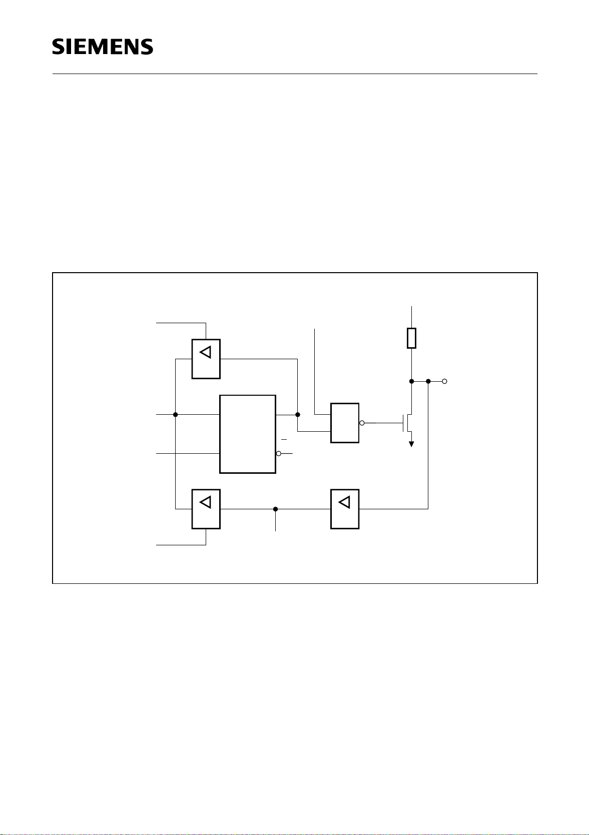
On-Chip Peripheral Components
C515C
6.1.2 Alternate Functions of Ports
Several pins of ports 1, 3, 4, and 7 are multifunctional. They are port pins and also serve to
implement special features as listed in table 6-1. The SSC interface pins of port 4 are described in
a previous section 6.1.1.2.4.
Figure 6-13 shows a functional diagram of a port latch with alternate function. To pass the alternate
function to the output pin and vice versa, however, the gate between the latch and driver circuit must
be open. Thus, to use the alternate input or output functions, the corresponding bit latch in the port
SFR has to contain a one (1); otherwise the pull-down FET is on and the port pin is stuck at 0. (This
does not apply to ports 1.0 to 1.3 when operating in compare output mode). After reset all port
latches contain ones (1).
Read
Latch
Int. Bus
Write
to
Latch
Read
Pin
D
CLK
Bit
Latch
Q
Q
Alternate
Input
Function
Alternate
Output
Function
V
CC
Internal
Pull Up
Arrangement
Pin
&
MCS01827
Figure 6-13
Circuitry of Ports 1, 3, 4 and 7
Port 5 has no alternate functions as described above. Therefore, the port circuitry has no switching
capability between alternate function and normal I/O operation. This more simple circuitry is shown
as basic port structure in figure 6-3.
The two CAN controller transmit/receive lines TXDC/RXDC are located as alternate functions on
the port 4 lines P4.6 and P4.7. These two port lines have the standard port structure which is equal
to port 1 or port 3.
Semiconductor Group 6-16 1997-10-01
Page 81

Table 6-1
Alternate Functions of Port Pins
Port Pin Alternate Function
On-Chip Peripheral Components
C515C
P1.0
P1.1
P1.2
P1.3
P1.4
P1.5
P1.6
P1.7
P3.0
P3.1
P3.2
P3.3
P3.4
P3.5
P3.6
P3.7
P4.0
P4.1
P4.2
P4.3
P4.4
P4.5
P4.6
P4.7
INT3
/CC0
INT4/CC1
INT5/CC2
INT6/CC3
INT2
T2EX
CLKOUT
T2
RXD
TXD
INT0
INT1
T0
T1
WR
RD
ADST
SCLK
SRI
STO
SLS
INT8
TXDC
RXDC
External interrupt 3/capture 0/compare 0
External interrupt 4/capture 1/compare 1
External interrupt 5/capture 2/compare 2
External interrupt 6/capture 3/compare 3
External interrupt 2
Timer 2 external reload trigger input
System clock output
Timer 2 external count input
Serial input channel 0
Serial output channel 0
External interrupt 0
External interrupt 1
Timer 0 external count input
Timer 1 external count input
External data memory write strobe
External data memory read strobe
A/D converter external start pin
SSC master clock output, SSC slave clock input
SSC receive input
SSC transmit output
SSC slave select input
External interrupt 8
CAN controller transmitter output
CAN controller receiver input
P7.0 INT7
Semiconductor Group 6-17 1997-10-01
External interrupt 7
Page 82
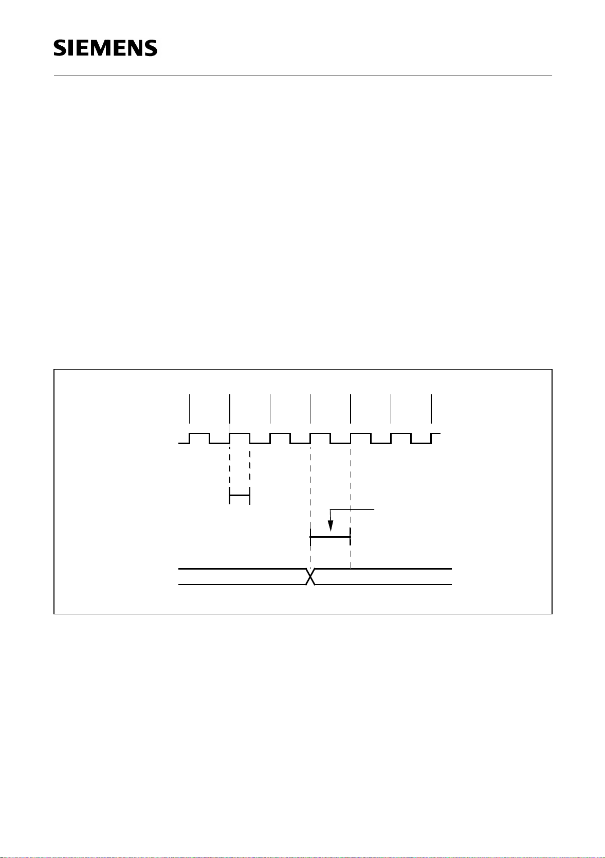
On-Chip Peripheral Components
C515C
6.1.3 Port Handling
6.1.3.1 Port Timing
When executing an instruction that changes the value of a port latch, the new value arrives at the
latch during S6P2 of the final cycle of the instruction. However, port latches are only sampled by
their output buffers during phase 1 of any clock period (during phase 2 the output buffer holds the
value it noticed during the previous phase 1). Consequently, the new value in the port latch will not
appear at the output pin until the next phase 1, which will be at S1P1 of the next machine cycle.
When an instruction reads a value from a port pin (e.g. MOV A, P1) the port pin is actually sampled
in state 5 phase 1 or phase 2 depending on port and alternate functions. Figure 6-14 illustrates this
port timing. lt must be noted that this mechanism of sampling once per machine cycle is also used
if a port pin is to detect an "edge", e.g. when used as counter input. In this case an "edge" is
detected when the sampled value differs from the value that was sampled the cycle before.
Therefore, there must be met certain requirements on the pulse length of signals in order to avoid
signal "edges" not being detected. The minimum time period of high and low level is one machine
cycle, which guarantees that this logic level is noticed by the port at least once.
Figure 6-14
Port Timing
P1 P2 P1 P2 P1 P2 P1 P2 P1 P2 P1 P2
XTAL1
Input sampled:
e.g.: MOV A, P1
Port
S4 S5 S6 S1 S2 S3
P1 active for 1 state
(driver transistor)
Old Data New Data
Semiconductor Group 6-18 1997-10-01
Page 83

On-Chip Peripheral Components
C515C
6.1.3.2 Port Loading and Interfacing
The output buffers of ports 1 to 5 and 7 can drive TTL inputs directly. The maximum port load which
still guarantees correct logic output levels can be looked up in the C515C DC characteristics in
chapter 10. The corresponding parameters are VOL and VOH.
The same applies to port 0 output buffers. They do, however, require external pullups to drive
floating inputs, except when being used as the address/data bus.
When used as inputs it must be noted that the ports 1 to 5 and 7 are not floating but have internal
pullup transistors. The driving devices must be capable of sinking a sufficient current if a logic low
level shall be applied to the port pin (the parameters ITL and IIL in the C515C DC characteristics
specify these currents). Port 0 has floating inputs when used for digital input.
6.1.3.3 Read-Modify-Write Feature of Ports 1 to 5 and 7
Some port-reading instructions read the latch and others read the pin. The instructions reading the
latch rather than the pin read a value, possibly change it, and then rewrite it to the latch. These are
called "read-modify-write"- instructions, which are listed in table 6-2. If the destination is a port or a
port pin, these instructions read the latch rather than the pin. Note that all other instructions which
can be used to read a port, exclusively read the port pin. In any case, reading from latch or pin,
respectively, is performed by reading the SFR P0, P1, P2 and P3; for example, "MOV A, P3" reads
the value from port 3 pins, while "ANL P3, #0AAH" reads from the latch, modifies the value and
writes it back to the latch.
It is not obvious that the last three instructions in table 6-2 are read-modify-write instructions, but
they are. The reason is that they read the port byte, all 8 bits, modify the addressed bit, then write
the complete byte back to the latch.
Table 6-2
Read-Modify-Write"- Instructions
Instruction Function
ANL Logic AND; e.g. ANL P1, A
ORL Logic OR; e.g. ORL P2, A
XRL Logic exclusive OR; e.g. XRL P3, A
JBC Jump if bit is set and clear bit; e.g. JBC P1.1, LABEL
CPL Complement bit; e.g. CPL P3.0
INC Increment byte; e.g. INC P1
DEC Decrement byte; e.g. DEC P1
DJNZ Decrement and jump if not zero; e.g. DJNZ P3, LABEL
MOV Px.y,C Move carry bit to bit y of port x
CLR Px.y Clear bit y of port x
SETB Px.y Set bit y of port x
Semiconductor Group 6-19 1997-10-01
Page 84

On-Chip Peripheral Components
C515C
The reason why read-modify-write instructions are directed to the latch rather than the pin is to avoid
a possible misinterpretation of the voltage level at the pin. For example, a port bit might be used to
drive the base of a transistor. When a "1" is written to the bit, the transistor is turned on. If the CPU
then reads the same port bit at the pin rather than the latch, it will read the base voltage of the
transistor (approx. 0.7 V, i.e. a logic low level!) and interpret it as "0". For example, when modifying
a port bit by a SETB or CLR instruction, another bit in this port with the above mentioned
configuration might be changed if the value read from the pin were written back to the latch.
However, reading the latch rater than the pin will return the correct value of "1".
Semiconductor Group 6-20 1997-10-01
Page 85

On-Chip Peripheral Components
C515C
6.2 Timers/Counters
The C515C contains three 16-bit timers/counters, timer 0, 1, and 2, which are useful in many
applications for timing and counting.
In "timer" function, the register is incremented every machine cycle. Thus one can think of it as
counting machine cycles. Since a machine cycle consists of 6 oscillator periods, the counter rate is
1/6 of the oscillator frequency.
In "counter" function, the register is incremented in response to a 1-to-0 transition (falling edge) at
its corresponding external input pin, T0 or T1 (alternate functions of P3.4 and P3.5, resp.). In this
function the external input is sampled during S5P2 of every machine cycle. When the samples show
a high in one cycle and a low in the next cycle, the count is incremented. The new count value
appears in the register during S3P1 of the cycle following the one in which the transition was
detected. Since it takes two machine cycles (12 oscillator periods) to recognize a 1-to-0 transition,
the maximum count rate is 1/12 of the oscillator frequency. There are no restrictions on the duty
cycle of the external input signal, but to ensure that a given level is sampled at least once before it
changes, it must be held for at least one full machine cycle.
6.2.1 Timer/Counter 0 and 1
Timer / counter 0 and 1 of the C515C are fully compatible with timer / counter 0 and 1 of the C501
and can be used in the same four operating modes:
Mode 0: 8-bit timer/counter with a divide-by-32 prescaler
Mode 1: 16-bit timer/counter
Mode 2: 8-bit timer/counter with 8-bit auto-reload
Mode 3: Timer/counter 0 is configured as one 8-bit timer/counter and one 8-bit timer; Timer/
counter 1 in this mode holds its count. The effect is the same as setting TR1 = 0.
External inputs INT0 and INT1 can be programmed to function as a gate for timer/counters 0 and 1
to facilitate pulse width measurements.
Each timer consists of two 8-bit registers (TH0 and TL0 for timer/counter 0, TH1 and TL1 for timer/
counter 1) which may be combined to one timer configuration depending on the mode that is
established. The functions of the timers are controlled by two special function registers TCON and
TMOD.
In the following descriptions the symbols TH0 and TL0 are used to specify the high-byte and the
low-byte of timer 0 (TH1 and TL1 for timer 1, respectively). The operating modes are described and
shown for timer 0. If not explicity noted, this applies also to timer 1.
Semiconductor Group 6-21 1997-10-01
Page 86
On-Chip Peripheral Components
e
6.2.1.1 Timer/Counter 0 and 1 Registers
Totally six special function registers control the timer/counter 0 and 1 operation :
– TL0/TH0 and TL1/TH1 - counter registers, low and high part
– TCON and TMOD - control and mode select registers
C515C
Special Function Register TL0 (Address 8AH) Reset Value : 00
Special Function Register TH0 (Address 8CH) Reset Value : 00
Special Function Register TL1 (Address 8BH) Reset Value : 00
Special Function Register TH1 (Address 8DH) Reset Value : 00
Bit No.
MSB LSB
76543210
H
H
H
H
.7 .6 .5 .48A
.7 .6 .5 .48C
.7 .6 .5 .48B
.7 .6 .5 .48D
.3 .2 .1 .0
TL0
TH0.3 .2 .1 .0
TL1.3 .2 .1 .0
TH1.3 .2 .1 .0
H
H
H
H
Bit Function
TLx.7-0
x=0-1
Timer/counter 0/1 low register
Operating Mode Description
0 "TLx" holds the 5-bit prescaler value.
1 "TLx" holds the lower 8-bit part of the 16-bit timer/counter value.
2 "TLx" holds the 8-bit timer/counter value.
3 TL0 holds the 8-bit timer/counter value; TL1 is not used.
THx.7-0
x=0-1
Timer/counter 0/1 high register
Operating Mode Description
0 "THx" holds the 8-bit timer/counter value.
1 "THx" holds the higher 8-bit part of the 16-bit timer/counter valu
2 "THx" holds the 8-bit reload value.
3 TH0 holds the 8-bit timer value; TH1 is not used.
Semiconductor Group 6-22 1997-10-01
Page 87

On-Chip Peripheral Components
C515C
Special Function Register TCON (Address 88H) Reset Value : 00
Bit No.
Bit Function
TR0 Timer 0 run control bit
TF0 Timer 0 overflow flag
TR1 Timer 1 run control bit
MSB LSB
76543210
8F
H
TF1 TR1 TF0 TR088
The shaded bits are not used in controlling timer/counter 0 and 1.
Set/cleared by software to turn timer/counter 0 ON/OFF.
Set by hardware on timer/counter overflow.
Cleared by hardware when processor vectors to interrupt routine.
Set/cleared by software to turn timer/counter 1 ON/OFF.
H
8E
H
8D
H
8C
8B
H
IE1 IT1 IE0 IT0
H
8A
H
89
H
88
H
TCON
H
TF1 Timer 1 overflow flag
Set by hardware on timer/counter overflow.
Cleared by hardware when processor vectors to interrupt routine.
Semiconductor Group 6-23 1997-10-01
Page 88
On-Chip Peripheral Components
C515C
Special Function Register TMOD (Address 89H) Reset Value : 00
Bit No.
MSB LSB
76543210
H
Gate C/T M1 M089
Gate C/T M1 M0
TMOD
Timer 1 Control Timer 0 Control
Bit Function
GATE Gating control
When set, timer/counter "x" is enabled only while "INT x" pin is high and "TRx"
control bit is set.
When cleared timer "x" is enabled whenever "TRx" control bit is set.
C/T Counter or timer select bit
Set for counter operation (input from "Tx" input pin).
Cleared for timer operation (input from internal system clock).
M1
M0
Mode select bits
M1 M0 Function
H
0 0 8-bit timer/counter:
"THx" operates as 8-bit timer/counter
"TLx" serves as 5-bit prescaler
0 1 16-bit timer/counter.
"THx" and "TLx" are cascaded; there is no prescaler
1 0 8-bit auto-reload timer/counter.
"THx" holds a value which is to be reloaded into "TLx" each
time it overflows
1 1 Timer 0 :
TL0 is an 8-bit timer/counter controlled by the standard
timer 0 control bits. TH0 is an 8-bit timer only controlled by
timer 1 control bits.
Timer 1 :
Timer/counter 1 stops
Semiconductor Group 6-24 1997-10-01
Page 89
On-Chip Peripheral Components
C515C
6.2.1.2 Mode 0
Putting either timer/counter 0,1 into mode 0 configures it as an 8-bit timer/counter with a divide-by32 prescaler. Figure 6-15 shows the mode 0 operation.
In this mode, the timer register is configured as a 13-bit register. As the count rolls over from all 1’s
to all 0’s, it sets the timer overflow flag TF0. The overflow flag TF0 then can be used to request an
interrupt. The counted input is enabled to the timer when TR0 = 1 and either Gate = 0 or INT0 = 1
(setting Gate = 1 allows the timer to be controlled by external input INT0, to facilitate pulse width
measurements). TR0 is a control bit in the special function register TCON; Gate is in TMOD.
The 13-bit register consists of all 8 bits of TH0 and the lower 5 bits of TL0. The upper 3 bits of TL0
are indeterminate and should be ignored. Setting the run flag (TR0) does not clear the registers.
Mode 0 operation is the same for timer 0 as for timer 1. Substitute TR0, TF0, TH0, TL0 and INT0 for
the corresponding timer 1 signals in figure 6-15. There are two different gate bits, one for timer 1
(TMOD.7) and one for timer 0 (TMOD.3).
OSC ÷ 6
C/T = 0
C/T = 1
P3.4/T0
Control
&
Gate
P3.2/INT0
= 1
TR0
_
<
1
Figure 6-15
Timer/Counter 0, Mode 0: 13-Bit Timer/Counter
TL0 TH0
(5 Bits) (8 Bits)
TF0
Interrupt
MCS02726
Semiconductor Group 6-25 1997-10-01
Page 90

On-Chip Peripheral Components
C515C
6.2.1.3 Mode 1
Mode 1 is the same as mode 0, except that the timer register is running with all 16 bits. Mode 1 is
shown in figure 6-16.
OSC ÷ 6
C/T = 0
P3.4/T0
C/T = 1
Control
TL0 TH0
(8 Bits) (8 Bits)
TF0
Interrupt
&
Gate
P3.2/INT0
= 1
TR0
_
<
1
Figure 6-16
Timer/Counter 0, Mode 1: 16-Bit Timer/Counter
MCS02727
Semiconductor Group 6-26 1997-10-01
Page 91
On-Chip Peripheral Components
C515C
6.2.1.4 Mode 2
Mode 2 configures the timer register as an 8-bit counter (TL0) with automatic reload, as shown in
figure 6-17. Overflow from TL0 not only sets TF0, but also reloads TL0 with the contents of TH0,
which is preset by software. The reload leaves TH0 unchanged.
÷ 6OSC
C/T = 0
P3.4/T0
C/T = 1
Control
TL0
(8 Bits)
TF0
Reload
Interrupt
&
TH0
(8 Bits)
Gate
P3.2/INT0
= 1
TR0
_
<
1
Figure 6-17
Timer/Counter 0,1, Mode 2: 8-Bit Timer/Counter with Auto-Reload
MCS02728
Semiconductor Group 6-27 1997-10-01
Page 92

On-Chip Peripheral Components
C515C
6.2.1.5 Mode 3
Mode 3 has different effects on timer 0 and timer 1. Timer 1 in mode 3 simply holds its count. The
effect is the same as setting TR1=0. Timer 0 in mode 3 establishes TL0 and TH0 as two seperate
counters. The logic for mode 3 on timer 0 is shown in figure 6-18. TL0 uses the timer 0 control bits:
C/T, Gate, TR0, INT0 and TF0. TH0 is locked into a timer function (counting machine cycles) and
takes over the use of TR1 and TF1 from timer 1. Thus, TH0 now controls the "timer 1" interrupt.
Mode 3 is provided for applications requiring an extra 8-bit timer or counter. When timer 0 is in mode
3, timer 1 can be turned on and off by switching it out of and into its own mode 3, or can still be used
by the serial channel as a baud rate generator, or in fact, in any application not requiring an interrupt
from timer 1 itself.
P3.4/T0
Gate
P3.2/INT0
TR1
= 1
f
/6
TR0
OSC
C/T = 0
C/T = 1
Control
&
÷ 6OSC
_
<
1
Timer Clock
TL0
(8 Bits)
TH0
(8 Bits)
TF0
TF1
Interrupt
Interrupt
MCS02729
Figure 6-18
Timer/Counter 0, Mode 3: Two 8-Bit Timers/Counters
Semiconductor Group 6-28 1997-10-01
Page 93

On-Chip Peripheral Components
C515C
6.2.2 Timer/Counter 2 with Additional Compare/Capture/Reload
The timer 2 with additional compare/capture/reload features is one of the most powerful peripheral
units of the C515C. lt can be used for all kinds of digital signal generation and event capturing like
pulse generation, pulse width modulation, pulse width measuring etc.
Timer 2 is designed to support various automotive control applications (ignition/injection-control,
anti-lock-brake ... ) as weil as industrial applications (DC-, three-phase AC- and stepper-motor
control, frequency generation, digital-to-analog conversion, process control ...). Please note that
this timer is not equivalent to timer 2 of the C501.
The C515C timer 2 in combination with the compare/capture/reload registers allows the following
operating modes:
– Compare : up to 4 PWM signals with 65535 steps at maximum, and 600 ns resolution
– Capture : up to 4 high speed capture inputs with 600 ns resolution
– Reload : modulation of timer 2 cycle time
The block diagram in figure 6-19 shows the general configuration of timer 2 with the additional
compare/capture/reload registers. The I/O pins which can used for timer 2 control are located as
multifunctional port functions at port 1 (see table 6-3).
Table 6-3
Alternate Port Functions of Timer 2
Pin Symbol Function
P1.7 / T2 External count or gate input to timer 2
P1.5 / T2EX External reload trigger input
P1.3 / INT6 / CC3 Compare output / capture input for CC register 3
P1.2 / INT5 / CC2 Compare output / capture input for CC register 2
P1.1 / INT4 / CC1 Compare output / capture input for CC register 1
P1.0 / INT3
/ CC0 Compare output / capture input for CRC register
Semiconductor Group 6-29 1997-10-01
Page 94

On-Chip Peripheral Components
C515C
Figure 6-19
Timer 2 Block Diagram
Semiconductor Group 6-30 1997-10-01
Page 95

On-Chip Peripheral Components
C515C
6.2.2.1 Timer 2 Registers
This chapter describes all timer 2 related special function registers of timer 2. The interrupt related
SFRs are also included in this section. Table 6-4 summarizes all timer 2 SFRs.
Table 6-4
Special Function Registers of the Timer 2 Unit
Symbol Description Address
T2CON
TL2
TH2
CRCL
CRCH
CCEN
CCL1
CCH1
CCL2
CCH2
CCL3
CCH3
IEN0
IEN1
IRCON
Timer 2 control register
Timer 2, low byte
Timer 2, high byte
Compare / reload / capture register, low byte
Compare / reload / capture register, high byte
Compare / capture enable register
Compare / capture register 1, low byte
Compare / capture register 1, high byte
Compare / capture register 2, low byte
Compare / capture register 2, high byte
Compare / capture register 3, low byte
Compare / capture register 3, high byte
Interrupt enable register 0
Interrupt enable register 1
Interrupt control register
C8
CC
CD
CA
CB
C1
C2
C3
C4
C5
C6
C7
A8
B8
C0
H
H
H
H
H
H
H
H
H
H
H
H
H
H
H
Semiconductor Group 6-31 1997-10-01
Page 96
On-Chip Peripheral Components
C515C
The T2CON timer 2 control register is a bitaddressable register which controls the timer 2 function
and the compare mode of registers CRC, CC1 to CC3.
Special Function Register T2CON (Address C8H) Reset Value : 00
Bit No.
MSB LSB
76543210
H
CF
T2PS I3FR I2FR T2R1C8
H
CE
H
CD
H
CC
H
CB
H
CA
H
C9
T2R0 T2CM T2I1 T2I0
H
C8
H
T2CON
The shaded bit is not used in controlling timer/counter 2.
Bit Function
T2PS Prescaler select bit
When set, timer 2 is clocked in the “timer“ or “gated timer“ function with 1/12 of the
oscillator frequency. When cleared, timer 2 is clocked with 1/6 of the oscillator
frequency. T2PS must be 0 for the counter operation of timer 2.
I3FR External interrupt 3 falling/rising edge flag
Used for capture function in combination with register CRC. lf set, a capture to
register CRC (if enabled) will occur on a positive transition at pin P1.0 / INT3
/ CC0.
lf I3FR is cleared, a capture will occur on a negative transition.
H
T2R1
Timer 2 reload mode selection
T2R0
T2R1 T2R0 Function
0 X Reload disabled
1 0 Mode 0 : auto-reload upon timer 2 overflow (TF2)
1 1 Mode 1 : reload on falling edge at pin T2EX / P1.5
T2CM Compare mode bit for registers CRC, CC1 through CC3
When set, compare mode 1 is selected. T2CM = 0 selects compare mode 0.
T2I1
T2I0
Timer 2 input selection
T2I1 T2I0 Function
0 0 No input selected, timer 2 stops
0 1 Timer function :
input frequency = f
/6 (T2PS = 0) or f
osc
1 0 Counter function : external input signal at pin T2 / P1-7
1 1 Gated timer function : input controlled by pin T2 / P1.7
/12 (T2PS = 1)
osc
Semiconductor Group 6-32 1997-10-01
Page 97
On-Chip Peripheral Components
C515C
Special Function Register TL2 (Address CCH) Reset Value : 00
Special Function Register TH2 (Address CDH) Reset Value : 00
Special Function Register CRCL (Address CAH) Reset Value : 00
Special Function Register CRCH (Address CBH) Reset Value : 00
Bit No.
MSB LSB
76543210
H
H
H
H
.7 .6 .5 .4CC
MSB .6 .5 .4CD
.7 .6 .5 .4CA
MSB .6 .5 .4CB
.3 .2 .1 LSB
TL2
TH2.3 .2 .1 .0
CRCL.3 .2 .1 LSB
CRCH.3 .2 .1 .0
H
H
H
H
Bit Function
TL2.7-0 Timer 2 value low byte
The TL2 register holds the 8-bit low part of the 16-bit timer 2 count value.
TH2.7-0 Timer 2 value high byte
The TH2 register holds the 8-bit high part of the 16-bit timer 2 count value.
CRCL.7-0 Compare / reload / capture register low byte
CRCL is the 8-bit low byte of the 16-bit reload register of timer 2. It is also used for
compare/capture functions.
CRCH.7-0 Compare / reload / capture register high byte
CRCH is the 8-bit high byte of the 16-bit reload register of timer 2. It is also used for
compare/capture functions.
Semiconductor Group 6-33 1997-10-01
Page 98
On-Chip Peripheral Components
C515C
Special Function Register IEN0 (Address A8H) Reset Value : 00
Special Function Register IEN1 (Address B8H) Reset Value : 00
Special Function Register IRCON (Address C0H) Reset Value : 00
MSB
Bit No. AF
A8
EAL WDT ET2 ES
H
Bit No. BF
B8
EXEN2 SWDT EX6 EX5
H
Bit No. C7
C0
EXF2 TF2 IEX6 IEX5
H
AE
H
AD
H
AC
H
AB
H
AA
H
A9
H
ET1 EX1 ET0 EX0
BE
H
BD
H
BC
H
BB
H
BA
H
B9
H
EX4 EX3 EX2 EADC
C6
H
C5
H
C4
H
C3
H
C2
H
C1
H
IEX4 IEX3 IEX2 IADC
LSB
A8
H
H
IEN0
H
B8
H
IEN1
C0
H
H
IRCON
The shaded bits are not used in timer/counter 2 interrupt control.
H
H
H
Bit Function
ET2 Timer 2 overflow / external reload interrupt enable.
If ET2 = 0, the timer 2 interrupt is disabled.
If ET2 = 1, the timer 2 interrupt is enabled.
EXEN2 Timer 2 external reload interrupt enable
If EXEN2 = 0, the timer 2 external reload interrupt is disabled.
If EXEN2 = 1, the timer 2 external reload interrupt is enabled. The external reload
function is not affected by EXEN2.
EXF2 Timer 2 external reload flag
EXF2 is set when a reload is caused by a falling edge on pin T2EX while EXEN2 =
1. If ET2 in IEN0 is set (timer 2 interrupt enabled), EXF2 = 1 will cause an interrupt.
EXF2 can be used as an additional external interrupt when the reload function is
not used. EXF2 must be cleared by software.
TF2 Timer 2 overflow flag
Set by a timer 2 overflow and must be cleared by software. If the timer 2 interrupt
is enabled, TF2 = 1 will cause an interrupt.
Semiconductor Group 6-34 1997-10-01
Page 99
On-Chip Peripheral Components
C515C
Special Function Register CCEN (Address C1H) Reset Value : 00
Bit No.
MSB LSB
76543210
H
COCAH3 COCAL3 COCAH2 COCAL2C1
COCAH1 COCAL1 COCAH0 COCAL0
CCEN
Bit Function
COCAH3
COCAL3
Compare/capture mode for CC register 3
COCAH3 COCAL3 Function
0 0 Compare/capture disabled
0 1 Capture on rising edge at pin P1.3 / INT6 / CC3
1 0 Compare enabled
1 1 Capture on write operation into register CCL3
COCAH2
Compare/capture mode for CC register 2
COCAL2
COCAH2 COCAL2 Function
H
COCAH1
COCAL1
COCAH0
COCAL0
0 0 Compare/capture disabled
0 1 Capture on rising edge at pin P1.2 / INT5 / CC2
1 0 Compare enabled
1 1 Capture on write operation into register CCL2
Compare/capture mode for CC register 1
COCAH1 COCAL1 Function
0 0 Compare/capture disabled
0 1 Capture on rising edge at pin P1.1 / INT4 / CC1
1 0 Compare enabled
1 1 Capture on write operation into register CCL1
Compare/capture mode for CRC register
COCAH0 COCAL0 Function
0 0 Compare/capture disabled
0 1 Capture on falling/rising edge at pin P1.0 / INT3
1 0 Compare enabled
/ CC0
1 1 Capture on write operation into register CRCL
Semiconductor Group 6-35 1997-10-01
Page 100

On-Chip Peripheral Components
C515C
6.2.2.2 Timer 2 Operation
The timer 2, which is a 16-bit-wide register, can operate as timer, event counter, or gated timer. The
control register T2CON and the timer/counter registers TL2/TH2 are described below.
Timer Mode
In timer function, the count rate is derived from the oscillator frequency. A prescaler offers the
possibility of selecting a count rate of 1/6 or 1/12 of the oscillator frequency. Thus, the 16-bit timer
register (consisting of TH2 and TL2) is either incremented in every machine cycle or in every second
machine cycle. The prescaler is selected by bit T2PS in special function register T2CON. lf T2PS is
cleared, the input frequency is 1/6 of the oscillator frequency. if T2PS is set, the 2:1 prescaler gates
1/12 of the oscillator frequency to the timer.
Gated Timer Mode
In gated timer function, the external input pin T2 (P1.7) functions as a gate to the input of timer 2. lf
T2 is high, the internal clock input is gated to the timer. T2 = 0 stops the counting procedure. This
facilitates pulse width measurements. The external gate signal is sampled once every machine
cycle.
Event Counter Mode
In the counter function, the timer 2 is incremented in response to a 1-to-0 transition at its
corresponding external input pin T2 (P1.7). In this function, the external input is sampled every
machine cycle. When the sampled inputs show a high in one cycle and a low in the next cycle, the
count is incremented. The new count value appears in the timer register in the cycle following the
one in which the transition was detected. Since it takes two machine cycles (12 oscillator periods)
to recognize a 1-to-0 transition, the maximum count rate is 1/6 of the oscillator frequency. There are
no restrictions on the duty cycle of the external input signal, but to ensure that a given level is
sampled at least once before it changes, it must be held for at least one full machine cycle.
Note: The prescaler must be off for proper counter operation of timer 2, i.e. T2PS must be 0.
In either case, no matter whether timer 2 is configured as timer, event counter, or gated timer, a
rolling-over of the count from all 1’s to all 0’s sets the timer overflow flag TF2 in SFR IRCON, which
can generate an interrupt.
lf TF2 is used to generate a timer overflow interrupt, the request flag must be cleared by the interrupt
service routine as it could be necessary to check whether it was the TF2 flag or the external reload
request flag EXF2 which requested the interrupt. Both request flags cause the program to branch to
the same vector address.
Semiconductor Group 6-36 1997-10-01
 Loading...