

Page 1
C509-L
8-Bit CMOS Microcontroller
User's Manual 10.97
http://www.siemens.de/
Semiconductor/
Page 2

C509-L Data Sheet
Revision History : 10.97
Previous Releases : 06.96 (Original Version)
Page (new
version)
1-6
1-11
3-1
3-12
4-12
6-6
6-28
6-78
6-85
6-88
6-93
7-13
7-16
11-1
11-3, 11-4
11-1, 11-5,
11-7
11-7 to11-9
Chapter 12
Page (prev.
version)
1-6
1-11
3-1
3-12
4-12
6-6
6-28
6-78
6-85
6-88
6-93
7-13
7-16
11-1
11-3
11-1, 11-5,
11-7
11-6 to11-8
Chapter 12
Subjects (changes since last revision)
Duty cycle for XTAL2 corrected
RESET : correction in text “for the duration of two machine cycles“
Correction in text : XRAM is internal
1st paragraph: sentence “Bit Swap is ...” added;
Table 3-2: Text in right column corrected
Figure 3-7; corrected and improved
Last paragraph og 4.4.2 : last sentence deleted
Correction in figure 6-4 and text : “Delay = 1 state“
Correction in text 2nd paragraph : “consists of three ...“
Abbreviations below table 6-10 added
Name of bit T1P2 corrected to T2P0
Formula for mode 1,3 baud rate corrected; last sentence added
Formula for mode A,B baud rate corrected
Several references in the text corrected from IRCON to IRCON0
Description of ICR and ICS added
V
modified
IL2
Improved and extended ICC specification
V
min. changed from 5V - 15% to 5V - 5%
CC
AC characteristics : 16 MHz clock oscillator duty cycle (DC) for
external clock changed to 0.45 to 0.55
Improved index; bold page numbers for main definition reference
Edition 10.97
Published by Siemens AG,
Bereich Halbleiter, MarketingKommunikation, Balanstraße 73,
81541 München
© Siemens AG 1997
All Rights Reserved.
Attention please!
As far as patents or other rights of third parties are concerned, liability is only assumed for components, not for
applications, processes and circuits implemented within components or assemblies.
The information describes the type of component and shall not be considered as assured characteristics.
Terms of delivery and rights to change design reserved.
For questions on technology, delivery and prices please contact the Semiconductor Group Offices in Germany or
the Siemens Companies and Representatives worldwide (see address list).
Due to technical requirements components may contain dangerous substances. For information on the types in
question please contact your nearest Siemens Office, Semiconductor Group.
Siemens AG is an approved CECC manufacturer.
Packing
Please use the recycling operators known to you. We can also help you – get in touch with your nearest sales
office. By agreement we will take packing material back, if it is sorted. You must bear the costs of transport.
For packing material that is returned to us unsorted or which we are not obliged to accept, we shall haveto invoice
you for any costs incurred.
Components used in life-support devices or systems must be expressly authorized for such purpose!
Critical components
systems
1 A critical component is a component used in a life-support device or system whose failure can reasonably be
2 Life support devices or systems are intended (a) to be implanted in the human body, or (b) to support and/or
2
with the express written approval of the Semiconductor Group of Siemens AG.
expected to cause the failure of that life-support device or system, or to affect its safety or effectiveness of that
device or system.
maintain and sustain human life. If they fail, it is reasonable to assume that the health of the user may be endangered.
1
of the Semiconductor Group of Siemens AG, may only be used in life-support devices or
Page 3

General Information
C509-L
Table of Contents Page
1 Introduction. . . . . . . . . . . . . . . . . . . . . . . . . . . . . . . . . . . . . . . . . . . . . . . . . . . . . . . 1-1
1.1 Pin Configuration . . . . . . . . . . . . . . . . . . . . . . . . . . . . . . . . . . . . . . . . . . . . . . . . . . . 1-4
1.2 Pin Definitions and Functions. . . . . . . . . . . . . . . . . . . . . . . . . . . . . . . . . . . . . . . . . . 1-5
2 Fundamental Structure . . . . . . . . . . . . . . . . . . . . . . . . . . . . . . . . . . . . . . . . . . . . . 2-1
2.1 CPU . . . . . . . . . . . . . . . . . . . . . . . . . . . . . . . . . . . . . . . . . . . . . . . . . . . . . . . . . . . . . 2-3
2.2 CPU Timing . . . . . . . . . . . . . . . . . . . . . . . . . . . . . . . . . . . . . . . . . . . . . . . . . . . . . . . 2-5
3 Memory Organization. . . . . . . . . . . . . . . . . . . . . . . . . . . . . . . . . . . . . . . . . . . . . . . 3-1
3.1 Program Memory, “Code Space” . . . . . . . . . . . . . . . . . . . . . . . . . . . . . . . . . . . . . . . 3-2
3.2 Data Memory, “Data Space”. . . . . . . . . . . . . . . . . . . . . . . . . . . . . . . . . . . . . . . . . . . 3-2
3.3 General Purpose Registers . . . . . . . . . . . . . . . . . . . . . . . . . . . . . . . . . . . . . . . . . . . 3-2
3.4 Program and Data Memory Organization. . . . . . . . . . . . . . . . . . . . . . . . . . . . . . . . . 3-3
3.4.1 Interface of External FLASH/ROM/EPROM and External SRAM Memory. . . . . . . . 3-4
3.4.2 Normal Mode Configuration . . . . . . . . . . . . . . . . . . . . . . . . . . . . . . . . . . . . . . . . . . . 3-5
3.4.3 XRAM Mode Configuration . . . . . . . . . . . . . . . . . . . . . . . . . . . . . . . . . . . . . . . . . . . 3-6
3.4.4 Bootstrap Mode Configuration . . . . . . . . . . . . . . . . . . . . . . . . . . . . . . . . . . . . . . . . . 3-7
3.4.5 Programming Mode Configuration . . . . . . . . . . . . . . . . . . . . . . . . . . . . . . . . . . . . . . 3-8
3.4.6 Special Function Register SYSCON1. . . . . . . . . . . . . . . . . . . . . . . . . . . . . . . . . . . 3-10
3.4.7 Operating Mode (Chipmode) Selection . . . . . . . . . . . . . . . . . . . . . . . . . . . . . . . . . 3-12
3.4.7.1 Special Software Unlock Sequence . . . . . . . . . . . . . . . . . . . . . . . . . . . . . . . . . . . . 3-13
3.4.7.2 Control Signals of the Chipmodes . . . . . . . . . . . . . . . . . . . . . . . . . . . . . . . . . . . . . 3-14
3.4.7.3 Switching of the SWAP-Bit . . . . . . . . . . . . . . . . . . . . . . . . . . . . . . . . . . . . . . . . . . . 3-15
3.4.8 Watchdog Timer - Behaviour in the Different Operating Modes. . . . . . . . . . . . . . . 3-16
3.5 Special Function Registers. . . . . . . . . . . . . . . . . . . . . . . . . . . . . . . . . . . . . . . . . . . 3-17
4 External Bus Interface . . . . . . . . . . . . . . . . . . . . . . . . . . . . . . . . . . . . . . . . . . . . . . 4-1
4.1 Accessing External Memory. . . . . . . . . . . . . . . . . . . . . . . . . . . . . . . . . . . . . . . . . . . 4-1
4.1.1 Role of P0 and P2 as Data/Address Bus . . . . . . . . . . . . . . . . . . . . . . . . . . . . . . . . . 4-1
4.1.2 Timing. . . . . . . . . . . . . . . . . . . . . . . . . . . . . . . . . . . . . . . . . . . . . . . . . . . . . . . . . . . . 4-2
4.1.3 External Program Memory Access. . . . . . . . . . . . . . . . . . . . . . . . . . . . . . . . . . . . . . 4-2
4.1.4 PSEN
4.1.5 Overlapping External Data and Program Memory Spaces. . . . . . . . . . . . . . . . . . . . 4-2
4.1.6 ALE, Address Latch Enable . . . . . . . . . . . . . . . . . . . . . . . . . . . . . . . . . . . . . . . . . . . 4-4
4.2 Enhanced Hooks Emulation Concept. . . . . . . . . . . . . . . . . . . . . . . . . . . . . . . . . . . . 4-5
4.3 Eight Datapointers for Faster External Bus Access . . . . . . . . . . . . . . . . . . . . . . . . . 4-6
4.3.1 The Importance of Additional Datapointers . . . . . . . . . . . . . . . . . . . . . . . . . . . . . . . 4-6
4.3.2 How the Eight Datapointers of the C509-L are Realized . . . . . . . . . . . . . . . . . . . . . 4-6
4.3.3 Advantages of Multiple Datapointers . . . . . . . . . . . . . . . . . . . . . . . . . . . . . . . . . . . . 4-7
4.3.4 Application Example and Performance Analysis . . . . . . . . . . . . . . . . . . . . . . . . . . . 4-7
4.4 XRAM Operation. . . . . . . . . . . . . . . . . . . . . . . . . . . . . . . . . . . . . . . . . . . . . . . . . . . 4-10
4.4.1 XRAM Access Control . . . . . . . . . . . . . . . . . . . . . . . . . . . . . . . . . . . . . . . . . . . . . . 4-10
4.4.2 Accesses to XRAM using the DPTR (16-bit Addressing Mode). . . . . . . . . . . . . . . 4-12
4.4.3 Accesses to XRAM using the Registers R0/R1 . . . . . . . . . . . . . . . . . . . . . . . . . . . 4-12
4.4.4 Reset Operation of the XRAM . . . . . . . . . . . . . . . . . . . . . . . . . . . . . . . . . . . . . . . . 4-16
4.4.5 Behaviour of Port0 and Port2 . . . . . . . . . . . . . . . . . . . . . . . . . . . . . . . . . . . . . . . . . 4-16
, Program Store Enable . . . . . . . . . . . . . . . . . . . . . . . . . . . . . . . . . . . . . . . . . 4-2
Semiconductor Group 1-1 1997-10-01
Page 4

General Information
C509-L
Table of Contents Page
5 Reset and System Clock Operation . . . . . . . . . . . . . . . . . . . . . . . . . . . . . . . . . . . 5-1
5.1 Reset Function and Circuitries . . . . . . . . . . . . . . . . . . . . . . . . . . . . . . . . . . . . . . . . . 5-1
5.2 Hardware Reset Timing . . . . . . . . . . . . . . . . . . . . . . . . . . . . . . . . . . . . . . . . . . . . . . 5-3
5.3 Fast Internal Reset after Power-On . . . . . . . . . . . . . . . . . . . . . . . . . . . . . . . . . . . . . 5-4
5.4 Reset Output Pin (RO
5.5 Oscillator and Clock Circuit. . . . . . . . . . . . . . . . . . . . . . . . . . . . . . . . . . . . . . . . . . . . 5-6
5.6 System Clock Output . . . . . . . . . . . . . . . . . . . . . . . . . . . . . . . . . . . . . . . . . . . . . . . . 5-8
6 On-Chip Peripheral Components . . . . . . . . . . . . . . . . . . . . . . . . . . . . . . . . . . . . . 6-1
6.1 Parallel I/O . . . . . . . . . . . . . . . . . . . . . . . . . . . . . . . . . . . . . . . . . . . . . . . . . . . . . . . . 6-1
6.1.1 Port Structures . . . . . . . . . . . . . . . . . . . . . . . . . . . . . . . . . . . . . . . . . . . . . . . . . . . . . 6-1
6.1.1.1 Port Structure Selection . . . . . . . . . . . . . . . . . . . . . . . . . . . . . . . . . . . . . . . . . . . . . . 6-3
6.1.1.2 Quasi-Bidirectional Port Structure . . . . . . . . . . . . . . . . . . . . . . . . . . . . . . . . . . . . . . 6-5
6.1.1.2.1 Basic Port Circuitry of Port 1 to 6 and 9 . . . . . . . . . . . . . . . . . . . . . . . . . . . . . . . . . . 6-5
6.1.1.2.2 Port 0 Circuitry . . . . . . . . . . . . . . . . . . . . . . . . . . . . . . . . . . . . . . . . . . . . . . . . . . . . 6-8
6.1.1.2.3 Port 0 and Port 2 used as Address/Data Bus. . . . . . . . . . . . . . . . . . . . . . . . . . . . . 6-9
6.1.1.3 Bidirectional (CMOS) Port Structure. . . . . . . . . . . . . . . . . . . . . . . . . . . . . . . . . . . . 6-10
6.1.1.3.1 Input Mode . . . . . . . . . . . . . . . . . . . . . . . . . . . . . . . . . . . . . . . . . . . . . . . . . . . . . . . 6-10
6.1.1.3.2 Output Mode. . . . . . . . . . . . . . . . . . . . . . . . . . . . . . . . . . . . . . . . . . . . . . . . . . . . . . 6-11
6.1.1.3.3 Hardware Power Down Mode. . . . . . . . . . . . . . . . . . . . . . . . . . . . . . . . . . . . . . . . . 6-13
6.1.2 Alternate Functions. . . . . . . . . . . . . . . . . . . . . . . . . . . . . . . . . . . . . . . . . . . . . . . . . 6-14
6.1.3 Port Handling . . . . . . . . . . . . . . . . . . . . . . . . . . . . . . . . . . . . . . . . . . . . . . . . . . . . . 6-16
6.1.3.1 Port Timing . . . . . . . . . . . . . . . . . . . . . . . . . . . . . . . . . . . . . . . . . . . . . . . . . . . . . . . 6-16
6.1.3.2 Port Loading and Interfacing. . . . . . . . . . . . . . . . . . . . . . . . . . . . . . . . . . . . . . . . . . 6-17
6.1.3.3 Read-Modify-Write Feature of Ports 1 to 6 and 9. . . . . . . . . . . . . . . . . . . . . . . . . . 6-17
6.2 Timer/Counter 0 and 1 . . . . . . . . . . . . . . . . . . . . . . . . . . . . . . . . . . . . . . . . . . . . . . 6-19
6.2.1 Timer/Counter 0 / 1 Registers. . . . . . . . . . . . . . . . . . . . . . . . . . . . . . . . . . . . . . . . . 6-20
6.2.2 Mode 0 . . . . . . . . . . . . . . . . . . . . . . . . . . . . . . . . . . . . . . . . . . . . . . . . . . . . . . . . . . 6-24
6.2.3 Mode 1 . . . . . . . . . . . . . . . . . . . . . . . . . . . . . . . . . . . . . . . . . . . . . . . . . . . . . . . . . . 6-25
6.2.4 Mode 2 . . . . . . . . . . . . . . . . . . . . . . . . . . . . . . . . . . . . . . . . . . . . . . . . . . . . . . . . . . 6-26
6.2.5 Mode 3 . . . . . . . . . . . . . . . . . . . . . . . . . . . . . . . . . . . . . . . . . . . . . . . . . . . . . . . . . . 6-27
6.3 The Compare/Capture Unit (CCU) . . . . . . . . . . . . . . . . . . . . . . . . . . . . . . . . . . . . . 6-28
6.3.1 Timer 2 Operation. . . . . . . . . . . . . . . . . . . . . . . . . . . . . . . . . . . . . . . . . . . . . . . . . . 6-33
6.3.1.1 Timer 2 Registers . . . . . . . . . . . . . . . . . . . . . . . . . . . . . . . . . . . . . . . . . . . . . . . . . . 6-33
6.3.1.2 Timer 2 Operating Modes. . . . . . . . . . . . . . . . . . . . . . . . . . . . . . . . . . . . . . . . . . . . 6-36
6.3.1.2.1 Gated Timer Mode . . . . . . . . . . . . . . . . . . . . . . . . . . . . . . . . . . . . . . . . . . . . . . . . . 6-37
6.3.1.2.2 Event Counter Mode. . . . . . . . . . . . . . . . . . . . . . . . . . . . . . . . . . . . . . . . . . . . . . . . 6-37
6.3.1.2.3 Reload of Timer 2. . . . . . . . . . . . . . . . . . . . . . . . . . . . . . . . . . . . . . . . . . . . . . . . . . 6-37
6.3.2 Operation of the Compare Timers . . . . . . . . . . . . . . . . . . . . . . . . . . . . . . . . . . . . . 6-39
6.3.2.1 Compare Timer and Compare Timer 1 Registers. . . . . . . . . . . . . . . . . . . . . . . . . . 6-39
6.3.2.2 Operating Modes of the Compare Timers . . . . . . . . . . . . . . . . . . . . . . . . . . . . . . . 6-42
6.3.3 Compare Functions of the CCU . . . . . . . . . . . . . . . . . . . . . . . . . . . . . . . . . . . . . . . 6-44
6.3.3.1 Compare Mode 0 . . . . . . . . . . . . . . . . . . . . . . . . . . . . . . . . . . . . . . . . . . . . . . . . . . 6-45
6.3.3.2 Compare Mode 1 . . . . . . . . . . . . . . . . . . . . . . . . . . . . . . . . . . . . . . . . . . . . . . . . . . 6-47
6.3.3.3 Compare Mode 2 . . . . . . . . . . . . . . . . . . . . . . . . . . . . . . . . . . . . . . . . . . . . . . . . . . 6-48
6.3.4 Timer- and Compare-Register Configurations of the CCU. . . . . . . . . . . . . . . . . . . 6-49
) . . . . . . . . . . . . . . . . . . . . . . . . . . . . . . . . . . . . . . . . . . . . . . . 5-6
Semiconductor Group 1-2 1997-10-01
Page 5

General Information
C509-L
Table of Contents Page
6.3.4.1 Timer 2 - Compare Function with Registers CRC, CC1 to CC3. . . . . . . . . . . . . . . 6-50
6.3.4.2 Timer 2 - Capture Function with Registers CRC, CC1 to CC4. . . . . . . . . . . . . . . . 6-53
6.3.4.3 Compare Function of Register CC4; “Concurrent Compare” . . . . . . . . . . . . . . . . . 6-55
6.3.4.4 Compare Function of Registers CM0 to CM7. . . . . . . . . . . . . . . . . . . . . . . . . . . . . 6-59
6.3.4.4.1 CMx Registers Assigned to the Compare Timer . . . . . . . . . . . . . . . . . . . . . . . . . . 6-60
6.3.4.4.2 CMx Registers Assigned to the Timer 2. . . . . . . . . . . . . . . . . . . . . . . . . . . . . . . . . 6-63
6.3.4.5 Timer 2 Operating in Compare Mode 2 . . . . . . . . . . . . . . . . . . . . . . . . . . . . . . . . . 6-64
6.3.4.6 Compare / Capture Operation with Compare Timer 1 . . . . . . . . . . . . . . . . . . . . . . 6-65
6.3.4.6.1 Compare Function of Registers CC10 to CC17 . . . . . . . . . . . . . . . . . . . . . . . . . . . 6-66
6.3.4.6.2 Capture Function of Registers CC10 to CC17 . . . . . . . . . . . . . . . . . . . . . . . . . . . . 6-68
6.3.5 Modulation Range in Compare Mode 0 . . . . . . . . . . . . . . . . . . . . . . . . . . . . . . . . . 6-69
6.3.6 Using Interrupts in Combination with the Compare Function . . . . . . . . . . . . . . . . . 6-71
6.3.6.1 Some advantages in using compare interrupts . . . . . . . . . . . . . . . . . . . . . . . . . . . 6-71
6.3.6.2 Interrupt Enable Bits of the Compare/Capture Unit . . . . . . . . . . . . . . . . . . . . . . . . 6-73
6.3.6.3 Interrupt Flags of the Compare/Capture Unit . . . . . . . . . . . . . . . . . . . . . . . . . . . . . 6-74
6.4 Arithmetic Unit . . . . . . . . . . . . . . . . . . . . . . . . . . . . . . . . . . . . . . . . . . . . . . . . . . . . 6-75
6.4.1 MDU Register. . . . . . . . . . . . . . . . . . . . . . . . . . . . . . . . . . . . . . . . . . . . . . . . . . . . . 6-75
6.4.2 Operation of the MDU. . . . . . . . . . . . . . . . . . . . . . . . . . . . . . . . . . . . . . . . . . . . . . . 6-77
6.4.3 Multiplication/Division . . . . . . . . . . . . . . . . . . . . . . . . . . . . . . . . . . . . . . . . . . . . . . . 6-78
6.4.4 Normalize and Shift . . . . . . . . . . . . . . . . . . . . . . . . . . . . . . . . . . . . . . . . . . . . . . . . 6-79
6.4.5 The Overflow Flag . . . . . . . . . . . . . . . . . . . . . . . . . . . . . . . . . . . . . . . . . . . . . . . . . 6-80
6.4.6 The Error Flag. . . . . . . . . . . . . . . . . . . . . . . . . . . . . . . . . . . . . . . . . . . . . . . . . . . . . 6-80
6.5 Serial Interfaces . . . . . . . . . . . . . . . . . . . . . . . . . . . . . . . . . . . . . . . . . . . . . . . . . . . 6-82
6.5.1 Serial Interface 0. . . . . . . . . . . . . . . . . . . . . . . . . . . . . . . . . . . . . . . . . . . . . . . . . . . 6-82
6.5.1.1 Operating Modes of Serial Interface 0 . . . . . . . . . . . . . . . . . . . . . . . . . . . . . . . . . . 6-82
6.5.1.2 Multiprocessor Communication Feature. . . . . . . . . . . . . . . . . . . . . . . . . . . . . . . . . 6-83
6.5.1.3 Baud Rates of Serial Channel 0 . . . . . . . . . . . . . . . . . . . . . . . . . . . . . . . . . . . . . . . 6-85
6.5.2 Serial Interface 1. . . . . . . . . . . . . . . . . . . . . . . . . . . . . . . . . . . . . . . . . . . . . . . . . . . 6-90
6.5.2.1 Operating Modes of Serial Interface 1 . . . . . . . . . . . . . . . . . . . . . . . . . . . . . . . . . . 6-90
6.5.2.2 Multiprocessor Communication Feature. . . . . . . . . . . . . . . . . . . . . . . . . . . . . . . . . 6-92
6.5.2.3 Baud Rates of Serial Channel 1 . . . . . . . . . . . . . . . . . . . . . . . . . . . . . . . . . . . . . . . 6-92
6.5.3 Detailed Description of the Operating Modes. . . . . . . . . . . . . . . . . . . . . . . . . . . . . 6-94
6.5.3.1 Mode 0, Synchronous Mode (Serial Interface 0) . . . . . . . . . . . . . . . . . . . . . . . . . . 6-94
6.5.3.2 Mode 1/Mode B, 8-Bit UART (Serial Interfaces 0 and 1) . . . . . . . . . . . . . . . . . . . . 6-97
6.5.3.3 Mode 2, 9-Bit UART (Serial Interface 0). . . . . . . . . . . . . . . . . . . . . . . . . . . . . . . . 6-100
6.5.3.4 Mode 3 / Mode A, 9-Bit UART (Serial Interfaces 0 and 1) . . . . . . . . . . . . . . . . . . 6-100
6.6 A/D Converter. . . . . . . . . . . . . . . . . . . . . . . . . . . . . . . . . . . . . . . . . . . . . . . . . . . . 6-104
6.6.1 A/D Converter Operation . . . . . . . . . . . . . . . . . . . . . . . . . . . . . . . . . . . . . . . . . . . 6-104
6.6.2 A/D Converter Registers. . . . . . . . . . . . . . . . . . . . . . . . . . . . . . . . . . . . . . . . . . . . 6-107
6.6.3 A/D Converter Clock Selection. . . . . . . . . . . . . . . . . . . . . . . . . . . . . . . . . . . . . . . 6-111
6.6.4 A/D Conversion Timing. . . . . . . . . . . . . . . . . . . . . . . . . . . . . . . . . . . . . . . . . . . . . 6-112
6.6.5 Adjustment of the Sample Time . . . . . . . . . . . . . . . . . . . . . . . . . . . . . . . . . . . . . . 6-116
6.6.6 A/D Converter Calibration. . . . . . . . . . . . . . . . . . . . . . . . . . . . . . . . . . . . . . . . . . . 6-118
Semiconductor Group 1-3 1997-10-01
Page 6

General Information
C509-L
Table of Contents Page
7 Interrupt System . . . . . . . . . . . . . . . . . . . . . . . . . . . . . . . . . . . . . . . . . . . . . . . . . . . 7-1
7.1 Structure of the Interrupt System . . . . . . . . . . . . . . . . . . . . . . . . . . . . . . . . . . . . . . . 7-1
7.2 Interrupt Registers . . . . . . . . . . . . . . . . . . . . . . . . . . . . . . . . . . . . . . . . . . . . . . . . . . 7-6
7.2.1 Interrupt Enable Registers . . . . . . . . . . . . . . . . . . . . . . . . . . . . . . . . . . . . . . . . . . . . 7-6
7.2.2 Interrupt Priority Registers . . . . . . . . . . . . . . . . . . . . . . . . . . . . . . . . . . . . . . . . . . . 7-10
7.2.3 Interrupt Request Flags . . . . . . . . . . . . . . . . . . . . . . . . . . . . . . . . . . . . . . . . . . . . . 7-11
7.3 Interrupt Priority Level Structure. . . . . . . . . . . . . . . . . . . . . . . . . . . . . . . . . . . . . . . 7-17
7.4 How Interrupts are Handled . . . . . . . . . . . . . . . . . . . . . . . . . . . . . . . . . . . . . . . . . . 7-19
7.5 External Interrupts . . . . . . . . . . . . . . . . . . . . . . . . . . . . . . . . . . . . . . . . . . . . . . . . . 7-21
7.6 Interrupt Response Time . . . . . . . . . . . . . . . . . . . . . . . . . . . . . . . . . . . . . . . . . . . . 7-22
8 Fail Save Mechanisms . . . . . . . . . . . . . . . . . . . . . . . . . . . . . . . . . . . . . . . . . . . . . . 8-1
8.1 Programmable Watchdog Timer. . . . . . . . . . . . . . . . . . . . . . . . . . . . . . . . . . . . . . . . 8-1
8.1.1 Input Clock Selection . . . . . . . . . . . . . . . . . . . . . . . . . . . . . . . . . . . . . . . . . . . . . . . . 8-2
8.1.2 Watchdog Timer Control Flags. . . . . . . . . . . . . . . . . . . . . . . . . . . . . . . . . . . . . . . . . 8-3
8.1.3 Starting the Watchdog Timer . . . . . . . . . . . . . . . . . . . . . . . . . . . . . . . . . . . . . . . . . . 8-4
8.1.3.1 The First Possibility of Starting the Watchdog Timer . . . . . . . . . . . . . . . . . . . . . . . . 8-4
8.1.3.2 The Second Possibility of Starting the Watchdog Timer. . . . . . . . . . . . . . . . . . . . . . 8-4
8.1.4 Refreshing the Watchdog Timer. . . . . . . . . . . . . . . . . . . . . . . . . . . . . . . . . . . . . . . . 8-5
8.1.5 Watchdog Reset and Watchdog Status Flag . . . . . . . . . . . . . . . . . . . . . . . . . . . . . . 8-5
8.2 Oscillator Watchdog . . . . . . . . . . . . . . . . . . . . . . . . . . . . . . . . . . . . . . . . . . . . . . . . . 8-6
9 Power Saving Modes . . . . . . . . . . . . . . . . . . . . . . . . . . . . . . . . . . . . . . . . . . . . . . . 9-1
9.1 Hardware Enable for the Use of the Power Saving Modes . . . . . . . . . . . . . . . . . . . 9-2
9.2 Power Saving Mode Control Register PCON. . . . . . . . . . . . . . . . . . . . . . . . . . . . . . 9-3
9.3 Idle Mode . . . . . . . . . . . . . . . . . . . . . . . . . . . . . . . . . . . . . . . . . . . . . . . . . . . . . . . . . 9-4
9.4 Software Power Down Mode . . . . . . . . . . . . . . . . . . . . . . . . . . . . . . . . . . . . . . . . . . 9-6
9.5 Slow Down Mode . . . . . . . . . . . . . . . . . . . . . . . . . . . . . . . . . . . . . . . . . . . . . . . . . . . 9-7
9.6 Hardware Power Down Mode. . . . . . . . . . . . . . . . . . . . . . . . . . . . . . . . . . . . . . . . . . 9-8
9.7 Hardware Power Down Mode Reset Timing. . . . . . . . . . . . . . . . . . . . . . . . . . . . . . 9-10
10 The Bootstrap Loader . . . . . . . . . . . . . . . . . . . . . . . . . . . . . . . . . . . . . . . . . . . . . 10-1
10.1 General Functions of the Bootstrap Loader . . . . . . . . . . . . . . . . . . . . . . . . . . . . . . 10-1
10.2 Phase I: Check for Existing Custom Software in the External FLASH Memory . . 10-3
10.2.1 Custom Software Check by the Info Block . . . . . . . . . . . . . . . . . . . . . . . . . . . . . . 10-3
10.2.2 Checksum Calculation. . . . . . . . . . . . . . . . . . . . . . . . . . . . . . . . . . . . . . . . . . . . . . 10-7
10.3 Phase II: Automatic Serial Synchronization with the Host. . . . . . . . . . . . . . . . . . . 10-8
10.3.1 Automatic Synchronization Procedure. . . . . . . . . . . . . . . . . . . . . . . . . . . . . . . . . . 10-9
10.3.2 Baud Rates for Correct Synchronization . . . . . . . . . . . . . . . . . . . . . . . . . . . . . . . 10-12
10.4 Phase III: Serial Communication with the Host . . . . . . . . . . . . . . . . . . . . . . . . . . 10-13
10.4.1 Block Transfer Protocol . . . . . . . . . . . . . . . . . . . . . . . . . . . . . . . . . . . . . . . . . . . . 10-13
10.4.1.1 Header Block Definition. . . . . . . . . . . . . . . . . . . . . . . . . . . . . . . . . . . . . . . . . . . . 10-15
10.4.1.2 Data and EOT Block Definition . . . . . . . . . . . . . . . . . . . . . . . . . . . . . . . . . . . . . . 10-16
10.4.2 Operating Mode Selection. . . . . . . . . . . . . . . . . . . . . . . . . . . . . . . . . . . . . . . . . . 10-17
10.4.2.1 Selection of Operating Mode 0. . . . . . . . . . . . . . . . . . . . . . . . . . . . . . . . . . . . . . . 10-19
10.4.2.2 Selection of Operating Mode 1. . . . . . . . . . . . . . . . . . . . . . . . . . . . . . . . . . . . . . . 10-23
10.4.2.3 Selection of Operating Mode 2. . . . . . . . . . . . . . . . . . . . . . . . . . . . . . . . . . . . . . . 10-24
Semiconductor Group 1-4 1997-10-01
Page 7

General Information
C509-L
Table of Contents Page
10.4.2.4 Selection of Operating Mode 3. . . . . . . . . . . . . . . . . . . . . . . . . . . . . . . . . . . . . . . 10-27
10.5 Description of the Bootstrap Loader Subroutines. . . . . . . . . . . . . . . . . . . . . . . . . 10-29
11 Device Specifications. . . . . . . . . . . . . . . . . . . . . . . . . . . . . . . . . . . . . . . . . . . . . . 11-1
11.1 Absolute Maximum Ratings . . . . . . . . . . . . . . . . . . . . . . . . . . . . . . . . . . . . . . . . . . 11-1
11.2 DC Characteristics . . . . . . . . . . . . . . . . . . . . . . . . . . . . . . . . . . . . . . . . . . . . . . . . . 11-1
11.3 A/D Converter Characteristics . . . . . . . . . . . . . . . . . . . . . . . . . . . . . . . . . . . . . . . . 11-5
11.4 AC Characteristics . . . . . . . . . . . . . . . . . . . . . . . . . . . . . . . . . . . . . . . . . . . . . . . . . 11-7
12 Index . . . . . . . . . . . . . . . . . . . . . . . . . . . . . . . . . . . . . . . . . . . . . . . . . . . . . . . . . . . 12-1
Semiconductor Group 1-5 1997-10-01
Page 8
Introduction
C509-L
1Introduction
The C509-L is a high-end microcontroller in the Siemens SAB-C500 8-bit microcontroller family. lt
is based on the well-known industry standard 8051 architecture; a great number of enhancements
and new peripheral features extend its capabilities to meet the extensive requirements of new
applications. Further, the C509-L is a superset of the Siemens SAB 80C517/80C517A 8-bit
microcontroller thus offering an easy upgrade path for SAB 80C517/80C517A users.
The high performance of the C509-L microcontroller is achieved by the C500-Core with a maximum
operating frequency of 16 MHz internal (and external) CPU clock. While maintaining all the features
of the SAB 80C517A, the C509-L is expanded by one I/O port, in its compare/capture capabilities,
by A/D converter functions, by additional 1 KByte of on-chip RAM (now 3 KByte XRAM) and by an
additional user-selectable CMOS port structure. The C509-L is mounted in a P-MQFP-100-2
package.
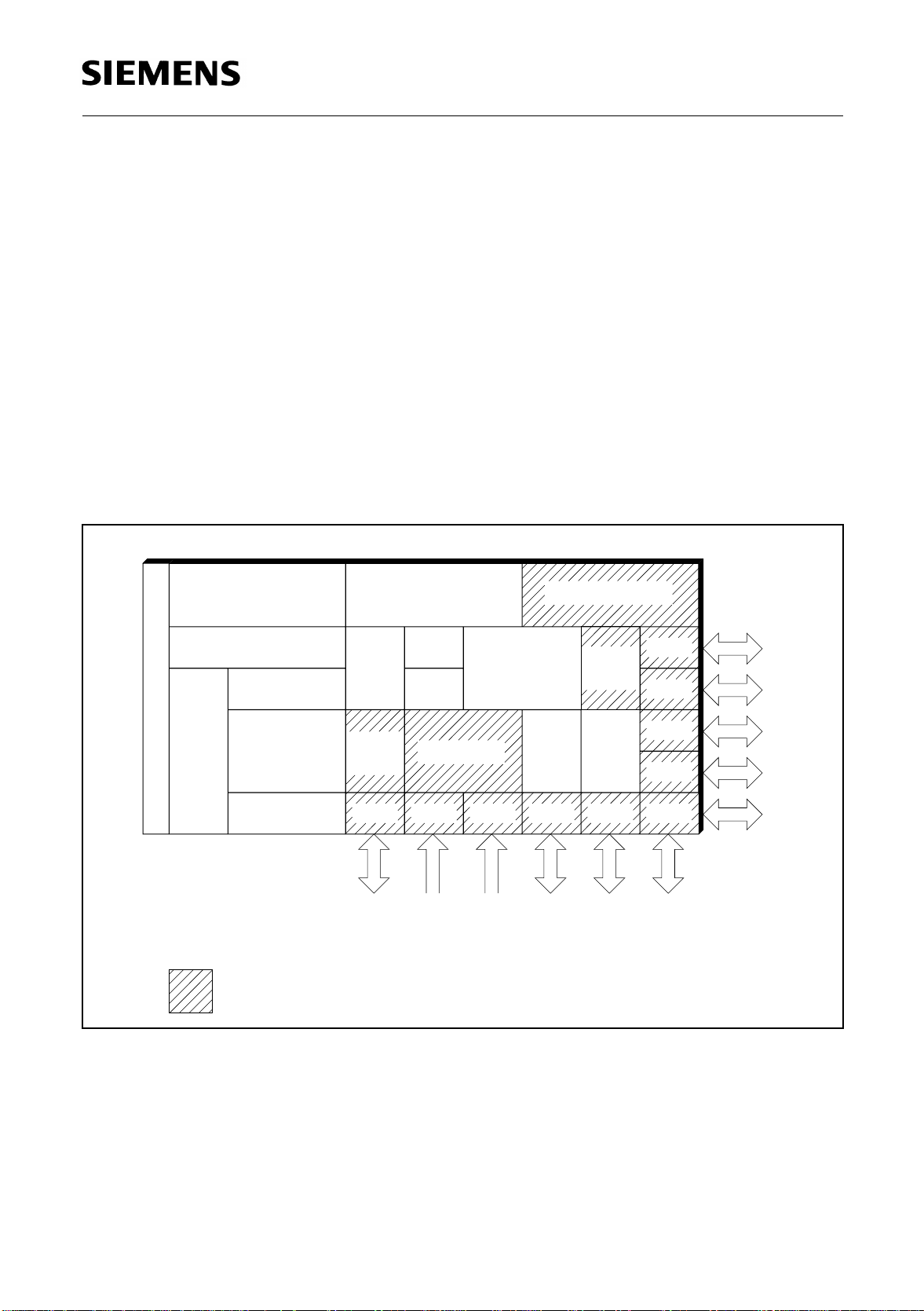
Figure 1-1 shows the different functional units of the C509-L and figure 1-2 shows the simplified
logic symbol of the C509-L.
C509
Watchdog
Oscillator
Watchdog
8-Bit UART
HW/SW
Power
Down
Modes
On-Chip Emulation Support Module
MDU
8-Bit USART
T 2
Comp.
Timer 1
Port 9 Port 8
I/O I/O I/O I/O
RAM
256 x 8
T 0
T 1
10-Bit ADC
analog/
digit.
input
CPU
C500-Core
(8-Dataptr)
Port 7
analog/
digit.
input
Boot ROM 512 x 8
XRAM
3 K x 8
CCU
Port 6
Comp.
Timer 1
Port 5
Port 4
Port 4
Port 4
Port 4
Port 4
I/O
I/O
I/O
I/O
I/O
Improved functionality in
comparison to the SAB 80C517A.
MCB02493
Figure 1-1
C509-L Functional Units
Semiconductor Group 1-1 1997-10-01
Page 9

Introduction
C509-L
Listed below is a summary of the main features of the C509-L:
l
Full upward compatibility with SAB 80C517/80C517A
l
256 byte on-chip RAM
l
3K byte of on-chip XRAM
l
256 directly addressable bits
l
375 ns instruction cycle at 16-MHz oscillator frequency
l
64 of 111 instructions are executed in one instruction cycle
l
External program and data memory expandable up to 64 Kbyte each
l
On-chip emulation support logic (Enhanced Hooks Technology
l
10-bit A/D converter
– 15 multiplexed inputs
– Built-in self calibration
l
Two 16-bit timers/counters (8051 compatible)
l
Three 16-bit timers/counters (can be used in combination with the compare/capture unit)
l
Powerful compare/capture unit (CCU) with up to 29 high-speed or PWM output channels or 13
capture inputs
l
Arithmetic unit for division, multiplication, shift and normalize operations
l
Eight datapointers instead of one for indirect addressing of program and external data memory
l
Extended watchdog facilities
– 15-bit programmable watchdog timer
– Oscillator watchdog
l
Ten I/O ports
– Eight bidirectional 8-bit I/O ports with selectable port structure
quasi-bidirectional port structure (8051 compatible)
bidirectional port structure with CMOS voltage levels
– One 8-bit and one 7-bit input port for analog and digital input signals
l
Two full-duplex serial interfaces with own baud rate generators
l
Four priority level interrupt systems, 19 interrupt vectors
l
Three power saving modes
– Slow-down mode
– Idle mode
– Power-down mode
l
Siemens high-performance ACMOS technology
l
M-QFP-100 rectangular quad flat package
l
Temperature Ranges : SAB-C509-L
SAF-C509-L
= 0 to 70 ° C
T
A
= -40 to 85 ° C
T
A
TM
)
Semiconductor Group 1-2 1997-10-01
Page 10
Introduction
C509-L
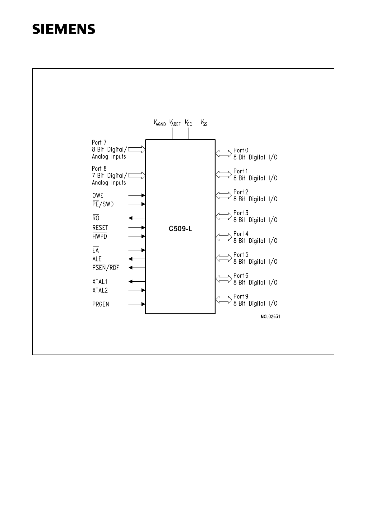
Figure 1-2
C509-L Logic Symbol
Semiconductor Group 1-3 1997-10-01
Page 11

Introduction
1.1 Pin Configuration
This section describes the pin configuration of the C509-L in the P-MQFP-100-2 package.
C509-L
Figure 1-3
C509-L Pin Configuration (P-MQFP-100-2, top view)
Semiconductor Group 1-4 1997-10-01
Page 12

1.2 Pin Definitions and Functions
This section describes all external signals of the C509-L with its function.
Table 1-1
Pin Definitions and Functions
Symbol Pin Number I/O*) Function
Introduction
C509-L
P1.0 - P1.7 9-6, 1,
100-98
9
8
7
6
1
100
99
98
I/O
Port 1
is an 8-bit bidirectional I/O port with internal pullup
resistors. Port 1 pins that have 1's written to them are
pulled high by the internal pullup resistors, and in that
state can be used as inputs. As inputs, port 1 pins being
externally pulled low will source current ( I
, in the DC
IL
characteristics) because of the internal pullup resistors.
Port 1 can also be switched into a bidirectional mode, in
which CMOS levels are provided. In this bidirectional
mode, each port 1 pin can be programmed individually
as input or output.
Port 1 also contains the interrupt, timer, clock, capture
and compare pins that are used by various options. The
output latch corresponding to a secondary function must
be programmed to a one (1) for that function to operate
(except when used for the compare functions).
The secondary functions are assigned to the pins of
port 1 as follows :
P1.0 INT3
CC0 Interrupt 3 input / compare 0 output /
capture 0 input
P1.1 INT4 CC1 Interrupt 4 input / compare 1 output /
capture 1 input
P1.2 INT5 CC2 Interrupt 5 input / compare 2 output /
capture 2 input
P1.3 INT6 CC3 Interrupt 6 input / compare 3 output /
capture 3 input
P1.4 INT2
CC4 Interrupt 2 input / compare 4 output /
capture 4 input
P1.5 T2EX Timer 2 external reload trigger input
P1.6 CLKOUT System clock output
P1.7 T2 Counter 2 input
*) I = Input
O = Output
Semiconductor Group 1-5 1997-10-01
Page 13

Table 1-1
Pin Definitions and Functions (cont’d)
Symbol Pin Number I/O*) Function
Introduction
C509-L
P9.0 - P9.7 74-77,
5-2
XTAL2 12 –
I/O
Port 9
is an 8-bit bidirectional I/O port with internal pullup resistors. Port 9 pins that have 1's written to them are pulled
high by the internal pullup resistors, and in that state can
be used as inputs. As inputs, port 9 pins being externally
pulled low will source current ( I
, in the DC characteri-
IL
stics) because of the internal pullup resistors.
Port 9 can also be switched into a bidirectional mode, in
which CMOS levels are provided. In this bidirectional
mode, each port 1 pin can be programmed individually
as input or output.
Port 9 also serves alternate compare functions. The output latch corresponding to a secondary function must be
programmed to a one (1) for that function to operate.
The secondary functions are assigned to the pins of
port 9 as follows :
P9.0-P9.7 CC10-CC17 Compare/capture channel 0-7
output/input
XTAL2
is the input to the inverting oscillator amplifier and input
to the internal clock generator circuits.
When supplying the C509-L with an external clock
source, XTAL2 should be driven, while XTAL1 is left
unconnected. A duty cycle of 0.45 to 0.55 of the clock
signal is required. Minimum and maximum high and low
times as well as rise/fall times specified in the AC
characteristics must be observed.
XTAL1 13 –
XTAL1
Output of the inverting oscillator amplifier. This pin is
used for the oscillator operation with crystal or ceramic
resonartor
*) I = Input
O = Output
Semiconductor Group 1-6 1997-10-01
Page 14
Table 1-1
Pin Definitions and Functions (cont’d)
Symbol Pin Number I/O*) Function
Introduction
C509-L
P2.0 – P2.7 14-21 I/O
PSEN
/ RDF 22 O
Port 2
is a 8-bit I/O port. Port 2 emits the high-order address
byte during fetches from external program memory and
during accesses to external data memory that use 16-bit
addresses (MOVX @DPTR). In this application it uses
strong internal pullup resistors when issuing 1s. During
accesses to external data memory that use 8-bit
addresses (MOVX @Ri), port 2 issues the contents of the
P2 special function register.
P2.0 - P2.7 A8 - A15 Address lines 8 - 15
Program Store Enable / Read FLASH
The PSEN
external program memory to the bus during external
code fetch operations. It is activated every third
oscillator period. PSEN is not activated during external
data memory accesses caused by MOVX instructions.
PSEN is not activated when instructions are executed
from the internal Boot ROM or from the XRAM.
In external programming mode RDF becomes active
when executing external data memory read (MOVX)
instructions.
output is a control signal that enables the
ALE 23 O
EA
PRGEN 25 I External Flash-EPROM Program Enable
*) I = Input
O = Output
24 I External Access Enable
Address Latch Enable
This output is used for latching the low byte of the
address into external memory during normal operation.
It is activated every third oscillator period except during
an external data memory access caused by MOVX
instructions.
The status of this pin is latched at the end of a reset.
When held at low level, the C509-L fetches all
instructions from the external program memory. For the
C509-L this pin must be tied low.
A low level at this pin disables the programming of an
external Flash-EPROM. To enable the programming of
an external Flash-EPROM, the pin PRGEN must be held
at high level and bit PRGEN1 in SFR SYSCON1 has to
be set. There is no internal pullup resistor connected to
this pin.
Semiconductor Group 1-7 1997-10-01
Page 15

Table 1-1
Pin Definitions and Functions (cont’d)
Symbol Pin Number I/O*) Function
Introduction
C509-L
P0.0 – P0.7 26, 27,
30-35
I/O Port 0
is an 8-bit open-drain bidirectional I/O port. Port 0 pins
that have 1s written to them float, and in that state can be
used as high-impendance inputs. Port 0 is also the
multiplexed low-order address and data bus during
accesses to external program or data memory. In this
operating mode it uses strong internal pullup resistors
when issuing 1 s.
P0.0 - P0.7 AD0-AD7 Address/data lines 0 - 7
HWPD
36 I Hardware Power Down
A low level on this pin for the duration of one machine
cycle while the oscillator is running resets the C509-L.
A low level for a longer period will force the part to power
down mode with the pins floating. There is no internal
pullup resistor connected to this pin.
P5.0 - P5.7 44-37 I/O Port 5
is an 8-bit bidirectional I/O port with internal pullup
resistors. Port 5 pins that have 1's written to them are
pulled high by the internal pullup resistors, and in that
state can be used as inputs. As inputs, port 5 pins being
externally pulled low will source current (I
characteristics) because of the internal pullup resistors.
Port 5 can also be switched into a bidirectional mode, in
which CMOS levels are provided. In this bidirectional
mode, each port 5 pin can be programmed individually
as input or output.
Port 5 also serves as alternate function for “Concurrent
Compare” and "Set/Reset compare” functions. The
output latch corresponding to a secondary function must
be programmed to a one (1) for that function to operate.
The secondary functions are assigned to the pins of port
5 as follows :
P5.0 - P5.7 CCM0-CCM7 Concurrent Compare
, in the DC
IL
or Set/Reset lines 0 - 7
*) I = Input
O = Output
Semiconductor Group 1-8 1997-10-01
Page 16

Table 1-1
Pin Definitions and Functions (cont’d)
Symbol Pin Number I/O*) Function
OWE 45 I Oscillator Watchdog Enable
A high level on this pin enables the oscillator watchdog.
When left unconnected, this pin is pulled high by a weak
internal pullup resistor. The logic level at OWE should
not be changed during normal operation. When held at
low level the oscillator watchdog function is turned off.
During hardware power down the pullup resistor is
switched off.
Introduction
C509-L
P6.0 - P6.7 46-50,
54-56
46
47
48
49
I/O Port 6
is an 8-bit bidirectional I/O port with internal pullup
resistors. Port 6 pins that have 1's written to them are
pulled high by the internal pullup resistors, and in that
state can be used as inputs. As inputs, port 6 pins being
externally pulled low will source current (I
characteristics) because of the internal pullup resistors.
Port 6 can also be switched into a bidirectional mode, in
which CMOS levels are provided. In this bidirectional
mode, each port 6 pin can be programmed individually
as input or output.
Port 6 also contains the external A/D converter control
pin, the receive and transmission lines for the serial
port 1, and the write-FLASH control signal. The output
latch corresponding to a secondary function must be
programmed to a one (1) for that function to operate.
The secondary functions are assigned to the pins of
port 6 as follows :
P6.0 ADST
P6.1 R×D1 Receiver data input of serial interface 1
P6.2 T×D1 Transmitter data output of serial
P6.3 WRF The WRF (write Flash) signal is active
, in the DC
IL
External A/D converter start pin
interface 1
when the programming mode is
selected. In this mode WRF becomes
active when executing external data
memory write (MOVX) instructions.
*) I = Input
O = Output
Semiconductor Group 1-9 1997-10-01
Page 17

Table 1-1
Pin Definitions and Functions (cont’d)
Symbol Pin Number I/O*) Function
Introduction
C509-L
P8.0 - P8.6 57-60,
51-53
RO
61 O Reset Output
P4.0 – P4.7 64-66,
68-72
I Port 8
is a 7-bit unidirectional input port. Port pins can be used
for digital input if voltage levels meet the specified input
high/low voltages, and for the higher 7-bit of the
multiplexed analog inputs of the A/D converter
simultaneously.
P8.0 - P8.6 AIN8 - AIN14 Analog input 8 - 14
This pin outputs the internally synchronized reset
request signal. This signal may be generated by an
external hardware reset, a watchdog timer reset or an
oscillator watchdog reset. The RO output is active low.
I/O Port 4
is an 8-bit bidirectional I/O port with internal pull-up
resistors. Port 4 pins that have 1’s written to them are
pulled high by the internal pull-up resistors, and in that
state can be used as inputs. As inputs, port 4 pins being
externally pulled low will source current (I
characteristics) because of the internal pull-up resistors.
Port 4 also erves as alternate compare functions. The
output latch corresponding to a secondary functionmust
be programmed to a one (1) for that function to operate.
The secondary functions are assigned to the pins of port
4 as follows :
P4.0 - P4.7 CM0 - CM7 Compare channel 0 - 7
, in the DC
IL
PE
/ SWD 67 I Power Saving Modes Enable / Start Watchdog Timer
A low level on this pin allows the software to enter the
power down mode, idle and slow down mode. If the low
level is also seen during reset, the watchdog timer
function is off on default.
Usage of the software controlled power saving modes is
blocked, when this pin is held on high level. A high level
during reset performs an automatic start of the watchdog
timer immediately after reset.
When left unconnected this pin is pulled high by a weak
internal pullup resistor. During hardware power down the
pullup resistor is switched off.
*) I = Input
O = Output
Semiconductor Group 1-10 1997-10-01
Page 18

Table 1-1
Pin Definitions and Functions (cont’d)
Symbol Pin Number I/O*) Function
RESET 73 I RESET
A low level on this pin for the duration of two machine
cycles while the oscillator is running resets the C509-L.
A small internal pullup resistor permits power-on reset
using only a capacitor connected to VSS.
Introduction
C509-L
V
V
AREF
AGND
78 – Reference voltage for the A/D converter
79 – Reference ground for the A/D converter
P7.0 - P7.7 87-80 I Port 7
Port 7 is an 8-bit unidirectional input port. Port pins can
be used for digital input if voltage levels meet the
specified input high/low voltages, and for the lower 8-bit
of the multiplexed analog inputs of the A/D converter
simultaneously.
P7.0 - P7.7 AIN0 - AIN7 Analog input 0 - 7
*) I = Input
O = Output
Semiconductor Group 1-11 1997-10-01
Page 19

Table 1-1
Pin Definitions and Functions (cont’d)
Symbol Pin Number I/O*) Function
Introduction
C509-L
P3.0 – P3.7 90-97
90
91
92
93
94
95
96
97
I/O Port 3
is an 8-bit bidirectional I/O port with internal pullup
resistors. Port 3 pins that have 1's written to them are
pulled high by the internal pullup resistors, and in that
state can be used as inputs. As inputs, port 3 pins being
externally pulled low will source current (I
characteristics) because of the internal pullup resistors.
Port 3 also contains two external interrupt inputs, the
timer 0/1 inputs, the serial port 0 receive/transmit line
and the external memory strobe pins. The output latch
corresponding to a secondary function must be
programmed to a one (1) for that function to operate.
The secondary functions are assigned to the port pins of
port 3 as follows
P3.0 R×D0 Receiver data input (asynchronous) or
P3.1 T×D0 Transmitter data output (asynchronous)
P3.2 INT0 Interrupt 0 input / timer 0 gate control
P3.3 INT1 Interrupt 1 input / timer 1 gate control
P3.4 T0 Counter 0 input
P3.5 T1 Counter 1 input
P3.6 WR
P3.7 RD / The read control signal enables the
, in the DC
IL
data input/output (synchronous) of serial
interface 0
or clock output (synchronous) of the
serial interface 0
The write control signal latches the data
byte from port 0 into the external data
memory
external data memory to port 0
PSENX PSENX (external program store enable)
enables the external code memory
when the external / internal XRAM
mode or external / internal programming
mode is selected.
V
SS
V
CC
*) I = Input
O = Output
10, 28, 62, 88 – Circuit ground potential
11, 29, 63, 89 – Supply terminal for all operating modes
Semiconductor Group 1-12 1997-10-01
Page 20

Fundamental Structure
C509-L
2 Fundamental Structure
The C509-L is the high-end 8051-compatible microcontroller of the C500 microcontroller family with
a significantly increased performance of CPU and peripheral units. It includes the complete
SAB 80C517A functionality, providing 100% upward compatibility. This means that all existing
80517A programs or user’s program libraries can be used further on without restriction and may be
easily extended to the C509-L.
Some of the various on-chip peripherals of the C509-L support the 8-bit core in case of stringent
real-time requirements. The 32-bit/16-bit arithmetic unit, the improved 4-level interrupt structure and
eight 16-bit datapointers are meant to give such a CPU support. But strict compatibility to the 8051
architecture is a principle of the C509-L design.
Furthermore, the C509-L contains eight 8-bit I/O ports and fifteen general input lines. The second
serial channel is compatible to the 8051-UART and provided with an independent and freely
programmable baud rate generator. An 10-bit resolution A/D-converter with built-in self calibration
has been integrated to allow analog signal processing. The C509-L further includes a powerful
compare/capture unit with two 16-bit compare timers for all kinds of digital signal processing. The
controller has been completed with well considered provisions for “fail-safe” reaction in critical
applications and offers all CMOS features like low power consumption as well as an idle, powerdown and slow-down mode.
Figure 2-1 shows the block diagram of the C509-L.
Semiconductor Group 2-1 1997-10-01
Page 21

Fundamental Structure
C509-L
Figure 2-1
Block Diagram of the C509-L
Semiconductor Group 2-2 1997-10-01
Page 22

Fundamental Structure
C509-L
2.1 CPU
The CPU is designed to operate on bits and bytes. The instructions, which consist of up to 3 bytes,
are performed in one, two or four machine cycles. One machine cycle requires six oscillator cycles
(this number of oscillator cycles differs from other members of the C500 microcontroller family). The
instruction set has extensive facilities for data transfer, logic and arithmetic instructions. The
Boolean processor has its own full-featured and bit-based instructions within the instruction set. The
C509-L uses five addressing modes: direct access, immediate, register, register indirect access,
and for accessing the external data or program memory portions a base register plus index-register
indirect addressing.Efficient use of program memory results from an instruction set consisting of
44 % one-byte, 41 % two-byte, and 15 % three-byte instructions. With a 16 MHz clock, 58 % of the
instructions execute in 375 ns.
The CPU (Central Processing Unit) of the C509-L consists of the instruction decoder, the arithmetic
section and the program control section. Each program instruction is decoded by the instruction
decoder. This unit generates the internal signals controlling the functions of the individual units
within the CPU. They have an effect on the source and destination of data transfers, and control the
ALU processing.
The arithmetic section of the processor performs extensive data manipulation and is comprised of
the arithmetic/logic unit (ALU), an A register, B register and PSW register.
The ALU accepts 8-bit data words from one or two sources and generates an 8-bit result under the
control of the instruction decoder. The ALU performs the arithmetic operations add, substract,
multiply, divide, increment, decrement, BDC-decimal-add-adjust and compare, and the logic
operations AND, OR, Exclusive OR, complement and rotate (right, left or swap nibble (left four)).
Also included is a Boolean processor performing the bit operations as set, clear, completement,
jump-if-not-set, jump-if-set-and-clear and move to/from carry. Between any addressable bit (or its
complement) and the carry flag, it can perform the bit operations of logical AND or logical OR with
the result returned to the carry flag.
The program control section controls the sequence in which the instructions stored in program
memory are executed. The 16-bit program counter (PC) holds the address of the next instruction to
be executed. The conditional branch logic enables internal and external events to the processor to
cause a change in the program execution sequence.
Accumulator
ACC is the symbol for the accumulator register. The mnemonics for accumulator-specific
instructions, however, refer to the accumulator simply as A.
Program Status Word
The Program Status Word (PSW) contains several status bits that reflect the current state of the
CPU.
Semiconductor Group 2-3 1997-10-01
Page 23
Fundamental Structure
C509-L
Special Function Register PSW (Address D0H) Reset Value : 00
Bit No. D7
D0
H
MSB
H
D6
H
D5
H
D4
CY AC F0 RS1
H
D3
H
D2
H
RS0 OV F1 P
D1
H
LSB
D0
H
PSW
Bit Function
CY Carry Flag
Used by arithmetic instructions.
AC Auxiliary Carry Flag
Used by instructions which execute BCD operations)
F0 General Purpose Flag
RS1
RS0
Register Bank select control bits
These bits are used to select one of the four register banks.
RS1 RS0 Function
H
0 0 Bank 0 selected, data address 00H-07
0 1 Bank 1 selected, data address 08H-0F
1 0 Bank 2 selected, data address 10H-17
1 1 Bank 3 selected, data address 18H-1F
H
H
H
H
OV Overflow Flag
F1 General Purpose Flag
Used by arithmetic instructions.
P Parity Flag
Set/cleared by hardware after each instruction cycle to indicate an odd/even
number of “one” bits in the accumulator, i.e. even parity.
B Register
The B register is used by 8-bit multiply and divide instructions and serves as both source and
destination. For other instructions it can be treated as another scratch pad register.
Stack Pointer
The stack pointer (SP) register is 8 bits wide. It is incremented before data is stored during PUSH
and CALL executions and decremented after data is popped during a POP and RET (RETI)
execution, i.e. it always points to the last valid stack byte. While the stack may reside anywhere in
the on-chip RAM, the stack pointer is initialized to 07H after a reset. This causes the stack to begin
a location = 08H above register bank zero. The SP can be read or written under software control.
Semiconductor Group 2-4 1997-10-01
Page 24

Fundamental Structure
C509-L
2.2 CPU Timing
A machine cycle consists of 6 states (6 oscillator periods). Each state is divided into a phase 1 half,
during OSC is high, and a phase 2 half, during which OSC is low. Thus, a machine cycle consists
of 6 oscillator periods, numbered S1P1 (state 1, phase 1) through S6P2 (state 6, phase 2). Each
state lasts for one oscillator period. Typically, arithmetic and logical operations take place during
phase 1 and internal register-to-register transfers take place during phase 2.
The diagrams in figure 2-2 show the fetch/execute timing related to the internal states and phases.
Since these internal clock signals are not user-accessible, the XTAL1 oscillator signals and the ALE
(address latch enable) signal are shown for external reference. ALE is normally activated twice
during each machine cycle: once during S1P2 and S2P1, and again during S4P2 and S5P1.
Executing of a one-cycle instruction begins at S1P2, when the op-code is latched into the instruction
register. If it is a two-byte instruction, the second reading takes place during S4 of the same
machine cycle. If it is a one-byte instruction, there is still a fetch at S4, but the byte read (which would
be the next op-code) is ignored (discarded fetch), and the program counter is not incremented. In
any case, execution is completed at the end of S6P2.
Figures 2-2 a) and b) show the timing of a 1-byte, 1-cycle instruction and for a 2-byte, 1-cycle
instruction.
Most C509-L instructions are executed in one cycle. MUL (multiply) and DIV (divide) are the only
instructions that take more than two cycles to complete; they take four cycles. Normally two code
bytes are fetched from the program memory during every machine cycle. The only exception to this
is when a MOVX instruction is executed. MOVX is a one-byte, 2-cycle instruction that accesses
external data memory. During a MOVX, the two fetches in the second cycle are skipped while the
external data memory is being addressed and strobed. Figure 2-2 c) and d) show the timing for a
normal 1-byte, 2-cycle instruction and for a MOVX instruction.
Semiconductor Group 2-5 1997-10-01
Page 25
Fundamental Structure
C509-L
Figure 2-2
Fetch and Execute Sequences
Semiconductor Group 2-6 1997-10-01
Page 26
Memory Organization
3 Memory Organization
The C509-L CPU manipulates data and operands in the following five address spaces:
– up to 64 Kbyte of external program memory
– up to 64 Kbyte of external data memory
– 512 byte of internal Boot ROM (program memory)
– 256 bytes of internal data memory
– 3 Kbyte of internal XRAM data memory
– a 128 byte special function register area
Figure 3-1 illustrates the memory address spaces of the C509-L.
C509-L
Figure 3-1
C509-L Memory Map
The internal XRAM data memory overlaps with the external data memory in the address range from
F400H to FFFFH. In this address range, either external or internal data RAM can be used. If the
internal XRAM has been enabled, it only can be disabled by an active RESET or HWPD signal.
The internal Boot ROM also overlaps with the external code memory in the address range from
0000H to 01FFH. Depending on the selected operating mode (chipmode), either external code
memory or the internal Boot ROM is accessed in this address range.
Semiconductor Group 3-1 1997-10-01
Page 27

Memory Organization
C509-L
3.1 Program Memory, “Code Space”
Besides the internal Boot ROM, the C509-L has no internal program memory (ROM). In normal
mode the program memory of the C509-L is located externally and can be expanded up to 64 Kbyte.
In the normal mode the C509-L fetches all instructions from the external program memory.
Therefore, the pin EA of the C509-L must be always tied to low level.
The Boot ROM includes a bootstrap loader program for the bootstrap mode of the C509-L. The
software routines of the bootstrap loader program allow the easy and quick programming or loading
of the internal XRAM (F400H to FFFFH) via the serial interface while the MCU is in-circuit. This
allows to transfer custom routines to the XRAM, which will program an external 64 KByte FLASH
memory. The routines of the bootstrap loader program may be executed or even can be blocked to
prevent unauthorized persons from reading out or writing to the external FLASH memory.
Therefore, the bootstrap loader checks an external FLASH memory for existing custom software
and executes it. The bootstrap loader program is described in detail in chapter 10.
3.2 Data Memory, “Data Space”
The data memory address space consists of an internal and an external memory space. The
internal data memory is divided into three physically separate and distinct blocks: the lower 128
bytes of RAM, the upper 128 bytes of RAM, and the 128 byte special function register (SFR) area.
While the upper 128 bytes of data memory and the SFR area share the same address locations,
they are accessed through different addressing modes. The lower 128 bytes of data memory can
be accessed through direct or register indirect addressing; the upper 128 bytes of RAM can be
accessed through register indirect addressing; the special function registers are accessible through
direct addressing. Four 8-register banks, each bank consisting of eight 8-bit multi-purpose registers,
occupy locations 0 through 1FH in the lower RAM area. The next 16 bytes, locations 20H through
2FH, contain 128 directly addressable bit locations. The stack can be located anywhere in the
internal data memory address space, and the stack depth can be expanded up to 256 bytes.
The external data memory can be expanded up to 64 Kbytes and can be accessed by instructions
that use a 16-bit or an 8-bit address. The internal XRAM is also located in the external data memory
area and must be accessed by external data memory instructions (MOVX). The XRAM can also
serve as code memory in the XRAM mode and in the FLASH programming mode. In these modes
program code which has been prior loaded via the bootstrap loader program, is executed in the
XRAM.
3.3 General Purpose Registers
The lower 32 locations of the internal RAM are assigned to four banks with eight general purpose
registers (GPRs) each. Only one of these banks may be enabled at a time. Two bits in the program
status word, RS0 (PSW.3) and RS1 (PSW.4), select the active register bank (see description of the
PSW in chapter 2). This allows fast context switching, which is useful when entering subroutines
or interrupt service routines.
The 8 general purpose registers of the selected register bank may be accessed by register
addressing. With register addressing the instruction op code indicates which register is to be used.
For indirect addressing R0 and R1 are used as pointer or index register to address internal or
external memory (e.g. MOV @R0).
Semiconductor Group 3-2 1997-10-01
Page 28

Memory Organization
C509-L
Reset initializes the stack pointer to location 07H and increments it once to start from location 08
H
which is also the first register (R0) of register bank 1. Thus, if one is going to use more than one
register bank, the SP should be initialized to a different location of the RAM which is not used for
data storage.
3.4 Program and Data Memory Organization
The C509-L can operate in four different operating modes (chipmodes) with different program and
data memory organizations:
– Normal Mode
– XRAM Mode
– Bootstrap Mode
– Programming Mode
Table 3-1 describes the program and data memory areas which are available in the different
chipmodes of the C509-L. It also shows the control bits of SFR SYSCON1, which are used for the
software selection of the chipmodes.
Table 3-1
Overview of Program and Data Memory Organization
Operating Mode
(Chipmode)
Program Memory Data Memory SYSCON1 Bits
Ext. Int. Ext. Int. PRGEN1SWAP
Normal Mode 0000
FFFF
H
H
XRAM Mode 0200H -
F3FF
H
Bootstrap Mode 0200H -
F3FF
H
Programming Mode 0200H -
FFFF
H
-
–
0000H 01FFH =
Boot ROM;
F400
H
-
FFFFH =
(XRAM)
0000H 01FFH =
Boot ROM
0000H 01FFH =
Boot ROM;
F400
H
-
FFFFH =
XRAM
0000H F3FF
H
0000
FFFF
H
H
-
(read only)
0000H F3FF
H
0000
FFFF
H
H
-
(read and
write)
F400
H
FFFF
H
(XRAM)
–
F400
H
FFFF
H
(XRAM)
–
-
00
01
-
10
11
Semiconductor Group 3-3 1997-10-01
Page 29

Memory Organization
C509-L
3.4.1 Interface of External FLASH/ROM/EPROM and External SRAM Memory
The external FLASH/ROM/EPROM memory and the external SRAM memory can be used in the
chipmodes either as code memory or as data memory. The basic memory configuration is shown
in figure 3-2.
The following alternate function pins control the read/write accesses for code/data memories:
PSEN / RDF Read control signal for the FLASH/ROM/EPROM memory
P6.3 / WRF Write control signal for the FLASH/ROM/EPROM memory
P3.6 / WR Write control signal for the SRAM memory
P3.7 / RD / PSENX Read control signal for the SRAM memory
Figure 3-2
Interface of External FLASH/ROM/EPROM and External SRAM Memory
Semiconductor Group 3-4 1997-10-01
Page 30
Memory Organization
C509-L
3.4.2 Normal Mode Configuration
The Normal Mode is the standard 8051 compatible operating mode of the C509-L. In this mode 64K
byte external code memory and 61K byte external SRAM as well as 3K byte internal data memory
(XRAM) are provided. If the XRAM is disabled (default after reset), totally 64K byte external data
memory are available. The Boot ROM is disabled. The external program memory is controlled by
the PSEN/RDF signal. Read and write accesses to the external data memory are controlled by the
RD and WR pins of port 3.
The Normal Mode is entered by keeping the pin PRGEN at a logic low during the rising edge of the
external RESET or HWPD signal. The locations of the code- and data-memory in Normal Mode are
shown in figure 3-4.
Figure 3-3
Locations of Code- and Data Memory in Normal Mode
Semiconductor Group 3-5 1997-10-01
Page 31

Memory Organization
C509-L
3.4.3 XRAM Mode Configuration
The XRAM Mode is implemented in the C509-L for executing e.g. up to 3K byte diagnostic software
which has been loaded into the XRAM in the Bootstrap Mode via the serial interface. In this
operating mode the Boot ROM, the XRAM, and the external data memory are mapped into the code
memory area, while the external ROM/EPROM is mapped into the external data memory area.
External program memory fetches from the SRAM are controlled by the P3.7/RD/PSENX pin.
External data memory read accesses from the ROM/EPROM are controlled by the PSEN/RDF pin.
In XRAM mode, the external data memory can only be read but not written.
The XRAM mode is entered by setting the SWAP bit, while the PRGEN pin (PRGEN1 bit) is kept
low. The locations of the code- and data-memory in the XRAM mode are shown in figure 3-4.
Figure 3-4
Locations of Code- and Data Memory in XRAM Mode
Notes: In the XRAM mode, programming of the external FLASH EPROM is not possible because
the PRGEN pin (PRGEN1 bit) is at logic low level (HW-protection).
The internal XRAM is selected automatically in the code memory, if the SWAP bit is set.
When leaving the XRAM Mode, the XRAM is disabled (only if the XMAP0 bit was not
cleared by software before).
Semiconductor Group 3-6 1997-10-01
Page 32

Memory Organization
C509-L
3.4.4 Bootstrap Mode Configuration
In the Bootstrap Mode the Boot ROM and the external FLASH/ROM/EPROM are mapped into the
code memory area. 61K byte external SRAM as well as 3K byte internal data memory (XRAM) are
provided in the external data memory area. The external program memory is controlled by the
PSEN/RDF signal. Read and write accesses to the external data memory are controlled by the RD
and WR pins of port 3.
The Bootstrap Mode is entered by keeping the pin PRGEN at a logic high level during the rising
edge of the external RESET or HWPD signal (→ PRGEN1=1). The locations of the code- and data
memory in the external boot-strap mode are shown in figure 3-5.
Figure 3-5
Locations of Code- and Data Memory in Bootstrap Mode
In Bootstrap Mode the internal XRAM is selected automatically as data memory. When leaving the
Bootstrap Mode, the XRAM is disabled (only if the XMAP0 bit was not cleared by software before).
Semiconductor Group 3-7 1997-10-01
Page 33

Memory Organization
C509-L
3.4.5 Programming Mode Configuration
The External Programming Mode is implemented for the in-circuit programming of external 5V-only
FLASH EPROMs. Similar as in the XRAM mode, the Boot ROM, the XRAM, and the external data
memory (SRAM) are mapped into the code memory area, while the external FLASH memory is
mapped into the external data memory area. Additionally to the XRAM mode, the FLASH memory
can also be written through external data memory accesses (MOVX instructions). External program
memory fetches from the SRAM are controlled by the P3.7/RD/PSENX pin. External data memory
read/write accesses from/to the ROM/EPROM are controlled by the PSEN/RDF and P6.3/WRF pin.
The Programming Mode is entered by setting the bits PRGEN1 and SWAP in SFR SYSCON1. The
locations of the code- and data memory in the Programming Mode are shown in figure 3-6.
Figure 3-6
Locations of Code- and Data Memory in Programming Mode
Prior to the usage of the Programming Mode, the XRAM has to be loaded by the FLASH specific
programming software algorithms (see also chapter 10 “The Bootstrap Loader”). This XRAM load
operation can be done using the Bootstrap Mode.
Semiconductor Group 3-8 1997-10-01
Page 34

Memory Organization
C509-L
Notes: The internal XRAM is enabled automatically in the code memory area if the SWAP bit is
set. When leaving the Programming Mode, the XRAM is disabled (only if the XMAP0 bit
was not cleared by software before).
Leaving the Programming Mode can be accomplished by:
– Clearing the bits PRGEN1 and SWAP prior to executing the special software unlock
sequence followed by a LJMP to “startaddress” in the FLASH memory returns the C509-L
into normal mode (program execution will start at “startaddress”).
– Activating the RESET or HWPD signal with the PRGEN pin at logic low level will clear the
bits PRGEN1 and SWAP.
Notes: Switching the PRGEN pin to logic low level during programming of an external FLASH will
reset the PRGEN1 bit. As a result the XRAM mode is entered and this inhibits any write
access to the external FLASH EPROM.
Clearing the SWAP bit during Programming Mode and executing the special software
unlock sequence will force the C509-L into the Bootstrap Mode.
Semiconductor Group 3-9 1997-10-01
Page 35

Memory Organization
C509-L
3.4.6 Special Function Register SYSCON1
There are five control bits located in SFR SYSCON1 (B2H) which control the code and data memory
organization of the C509-L. Two of these bits (PRGEN1 and SWAP) cannot be programmed as
normal bits but with a special software unlock sequence. The special software unlock sequence
was implemented to prevent unintentional changing of these bits and consists of consecutive
followed instructions which have to set two dedicated enable bits.
Special Function Register SYSCON1 (Address B2H) Reset Value : 00XXXEE0
B
1)
MSB
Bit No. 76543210
B2
ESWC SWC – EA1
H
1) “E” means that the value of the bit is defined through the external logic level at
pin PRGEN at the rising edge of the external RESET
EA0
PRGEN1PRGEN0 SWAP
or HWPD signals.
Bit Function
ESWC Enable Switch Chipmode
When selecting the chipmode with the bits SWAP and PRGEN1, the ESWC bit has
to be set simultaneously as the first instruction in the special software unlock
sequence. The bit ESWC will be cleared by hardware after 2 instruction cycles.
SWC Switch Chip Mode
The SWC bit has to be set as the second instruction in a special software unlock
sequence directly after having set bit ESWC. The new chipmode becomes active
after the second instruction cycle which follows the special software unlock
sequence. These two instruction cycles are used for initializing of the program
counter (LJMP instruction)
SWC is a write only bit. Reading SWC will always return a ‘0’.
LSB
SYSCON1
–, EA1, EA0 Reserved bits; at read operations these bits are undefined; at write operations to
SYSCON1 these bits can be written with “0” or “1”.
PRGEN1 Program Enable Bit 1
The PRGEN1 bit enables/disables the write accesses to an external FLASH
EPROM. The PRGEN1 bit contains the logic value of the external PRGEN pin
which is latched at the rising edge of the external RESET
or HWPD signal. When
the logic low level appears at the PRGEN pin, the PRGEN1 bit will be cleared in the
next instruction cycle without the need of a special software unlock sequence.
PRGEN1 = 0: Write access (programming) of external FLASH EPROM is
disabled
PRGEN1 = 1: Write access (programming) of external FLASH EPROM is
enabled
Any changing the PRGEN1 bit without using a special software unlock sequence
with the ESWC and SWC bits will have no effect and the former selected status will
be kept.
Semiconductor Group 3-10 1997-10-01
Page 36

Bit Function
PRGEN0 Program Enable Bit 0
The PRGEN0 bit is a read-only bit and represents the logic level of the external
PRGEN pin.
PRGEN0 = 1: The PRGEN1 bit can be set or cleared under software control.
PRGEN0 = 0: The PRGEN1 bit is held at logic low level and cannot be set under
software control.
Notes: Clearing the PRGEN0 bit by changing the logic level at the PRGEN pin in
the Normal Mode disables write accesses to the external FLASH EPROM.
Enable/disable write accesses to external FLASH EPROM can be done by
changing the PRGEN1 bit with a special software unlock sequence.
SWAP Swap Code- and Data Memory
SWAP = 0: The data memory and the code memory remain in their predefined
locations.
SWAP = 1: The following address areas and memory locations are assigned to
code memory:
0000H - 01FF
0200H - F3FF
F400H - FFFF
The following address areas and memory locations ar assigned to
data memory:
0000H - FFFF
H
H
H
H
Memory Organization
C509-L
→ Boot ROM
→ External data memory is swapped to external
code memory
→ The XRAM is enabled and automatically
mapped into code memory space.
(independent of bit XMAP0 in SFR SYSCON)
→ External FLASH /ROM/EPROM
The former code memory is assigned as data
memory and is now addressable by using
MOVX instructions.
Semiconductor Group 3-11 1997-10-01
Page 37

Memory Organization
C509-L
3.4.7 Operating Mode (Chipmode) Selection
The chipmode selection can be done by hardware after an active RESET or HWPD signal. Further,
the logic state of pin PRGEN is used for hardware selection. Bit Swap is not affected by hardware
selection. The chipmodes can also be selected by software. Software selection is achieved by
programming specific bits of SFR SYSCON1.
The following table 3-2 shows the hardware and software selection capabilities of the chipmodes.
Table 3-2
Hardware and Software Selection of Chipmodes
Operating Mode
Hardware Selection Software Selection
(Chipmode)
Normal Mode PRGEN pin = low
RESET or HWPD: edge
PRGEN pin = don’t care;
1 4
setting bits PRGEN1,SWAP = 0,0;
executing unlock sequence
XRAM Mode from Programming Mode:
setting PRGEN pin = low
PRGEN pin = don’t care;
2 5
setting bits PRGEN1,SWAP = 0,1;
executing unlock sequence
Bootstrap Mode PRGEN pin = high
RESET or HWPD: edge
PRGEN pin = high;
3 6
setting bits PRGEN1,SWAP =1,0;
executing unlock sequence
Programming Mode not possible PRGEN pin = high;
7
setting bits PRGEN1,SWAP = 1,1;
executing unlock sequence
Figure 3-7 below shows the information of table 3-2 as a state diagram (reference number in the
circle).
1
Normal Mode
PRGEN1, SWAP = 0,0
4
7
XRAM Mode
PRGEN1, SWAP = 0,1
5
6
5
2
5
3
4
7
6
Bootstrap Mode
PRGEN1, SWAP = 1,0
4
Programming Mode
PRGEN1, SWAP = 1,1
7
6
Hardware Selection
Software Selection
MCD02645
Figure 3-7
State Diagram of Chipmode Selection
Semiconductor Group 3-12 1997-10-01
Page 38

Memory Organization
C509-L
3.4.7.1 Special Software Unlock Sequence
The bits ESWC and SWC in SFR SYSCON1 are implemented in a way to prevent unintentional
changing of the bits SWAP or PRGEN1. Any changing the bits SWAP or PRGEN1 without using
the ESWC and SWC bits in a special software unlock sequence will have no effect and the above
bits will get back their old values two instruction cycles after being changed.
The following programming steps must be executed at the ESWC/SWC unlock sequence:
1.) First instruction:
Changing the value of the bits SWAP or PRGEN1 with one or more consecutive instructions
simultaneously with setting of bit ESWC:
ANL SYSCON1, #11111X1YB ; clearing of bits PRGEN1 (X=0) and/or SWAP (Y=0)
ORL SYSCON1, #10000X0YB ; setting of ESWC bit with setting of PRGEN1 or SWAP
; e.g. clearing of the SWAP bit:
ANL SYSCON1,#11111110B
ORL SYSCON1,#10000000B
or:
ORL SYSCON1, #10000X0YB ; setting of the bits PRGEN1 (X=1) and/or SWAP (Y=1) and
; setting the ESWC bit simultaneously
; e.g. setting of the SWAP bit:
ORL SYSCON1,#10000001B
2.) Second instruction:
Setting of bit SWC immediately after 1.) with
ORL SYSCON1, #40H ;
The new chipmode becomes active two instruction cycles after the instruction which sets the bit
SWC (see 2.). These two instruction cycle delay should normally be used for initialization of the
program counter to the 16 bit start-address of the new code memory resource, e.g. with:
LJMP 0XXXXH ; XXXX = 16-bit hex address in new code memory
If the code memory resource is not changed by the new chipmode there is no need of a new
initialization of the program counter. However the new Chipmode becomes active two instruction
cycles after 2.).
The special software unlock instruction sequence cannot be interrupted by an interrupt request. Any
write or read operation to SFR SYSCON1 will block the interrupt generation for the first cycle of the
directly following instruction.Therefore, the response time of an interrupt request may be
additionally delayed from minimal five instruction cycles up to eight instruction cycles: four or six
instruction cycles for setting ESWC and SWC (depends on the used instructions) and one or two
instruction cycles depending on the instruction used in 3.). When using a one cycle instruction in 3.)
an enabled interrupt may be performed and the interrupt vector address may reside in a “new” code
memory resource due to the new selected Chipmode.
The bits SWAP and PRGEN1 are built up by three shadow latches each. Unintentional changing of
one of this three latches (e.g. by RFI) will have no effect and the former value will be restored in the
next instruction cycle.
Semiconductor Group 3-13 1997-10-01
Page 39

Memory Organization
C509-L
3.4.7.2 Control Signals of the Chipmodes
As shown in chapter 3.4.2 to 3.4.5, each chipmode uses specific read/write control signals,
Table 3-3 gives a detailed survey about each chipmode and its control signals.
Table 3-3
Usage of Control Signals in the different Chipmodes
Operating Mode
(Chipmode)
Code Memory Control Data Memory Control
PSEN
/
RDF
Normal Mode 0000
XRAM Mode
FFFF
–
H
H
Bootstrap Mode 0200H -
FFFF
H
Programming
–
Mode
-
P3.7 / RD /
PSENX
–
0200H F3FF
–
0200H F3FF
H
H
P3.7 / RD /
P3.6 / WR PSEN /
PSENX
XMAP0=1 :
0000
H
FFFF
H
XMAP0=0 :
0000
H
F3FF
H
––
0000
H
F3FF
H
––
-
-
-
XMAP0=1 :
0000
FFFF
H
H
-
XMAP0=0 :
0000
F3FF
0000
F3FF
H
H
H
H
-
-
P6.3 /
RDF
––
0000
H
FFFF
H
––
0000
H
FFFF
H
WRF
–
-
-
0000
FFFF
H
H
-
Semiconductor Group 3-14 1997-10-01
Page 40

Memory Organization
C509-L
3.4.7.3 Switching of the SWAP-Bit
Setting or clearing the SWAP-bit in SYSCON1 will change code memory and data memory
assignment. To assure a well defined behavior of the controller, it is necessary to perform a specific
code sequence by the user. Any write access to SYSCON1 which changes the SWAP bit has to be
followed by a 2-cycle instruction. This 2-cycle instruction will be the last instruction, which is
performed by the CPU in the former code memory. For that reason, this 2-cycle instruction has to
be a LJMP-instruction which specifies the new address for the program counter. The next
instruction, which will be performed by the CPU is at the specified destination address of the JMP
instruction in the former data memory (which now has become to code memory).
Figure 3-8 gives an overview about the behavior of the external pin PSEN/RDF and RD/PSENX
when chipmodes with different SWAP bits are switched. These signals change their functions
depending on the value of the SWAP bit.
Figure 3-8
Switching of the SWAP Bit
Figure 3-8 a): When the SWAP bit is set, the “program store enable” function of the PSEN
which is connected to OE (output enable) of the FLASH/ROM/EPROM memory, is switched to the
/PSENX pin. The “read enable” function of the RD/PSENX pin, which is connected to the RD
RD
(“read“) input of an external SRAM memory, is switched to the PSEN/RDF signal. PSEN/RDF
becomes now active during MOVX instructions.
When the SWAP bit is cleared, the “read enable” function (MOVX instructions) of the PSEN/RDF
pin, which is connected to OE (output enable) of the FLASH/ROM/EPROM memory, is switched to
the RD/PSENX pin. The “program store enable” function of the RD/PSENX pin, which is connected
to the RD (“read“) input of the external SRAM memory, is switched to the PSEN/RDF pin. RD/
PSENX becomes now active during MOVX instructions.
Semiconductor Group 3-15 1997-10-01
/RDF pin,
Page 41

Memory Organization
C509-L
3.4.8 Watchdog Timer - Behaviour in the Different Operating Modes
This section describes the chipmode specific behavior of the watchdog timer unit. Further details
about the watchdog timer are given in chapter 8.
Normal Mode:
The watchdog timer function in Normal Mode is not restricted.
XRAM Mode:
To avoid deadlocks during program execution in the XRAM, the once enabled watchdog timer
keeps on running but the refresh is inhibited. A refresh sequence of a previously enabled watchdog
timer is not permitted. An unintentional refresh sequence in the XRAM mode does not reload the
watchdog timer and an internally generated watchdog reset will be executed at the watchdog
counter state 7FFCH. The watchdog timer reset generation is enabled.
For refreshing the watchdog timer, the user has to leave the XRAM Mode and must enter the
Normal Mode by clearing the SWAP bit followed by a LJMP or LCALL to “startaddress of watchdog
timer refresh” in the external ROM/EPROM. In the normal mode the watchdog timer refresh can be
executed successfully. If required, XRAM Mode can again be entered after the watchdog timer
refresh operation has been finished.
Bootstrap Mode and Programming Mode
In the Bootstrap Mode and in the Programming Mode the watchdog timer increment is inhibited. In
this way, programming the external FLASH EPROM in Programming Mode cannot be aborted by
the watchdog timer.
Semiconductor Group 3-16 1997-10-01
Page 42

Memory Organization
C509-L
3.5 Special Function Registers
The registers, except the program counter and the four general purpose register banks, reside in
the special function register area. The special function register area consists of two portions: the
standard special function register area and two mapped special function register areas. Several
special function registers of the C509-L (CC10-17, CT1REL, CC1EN, CAFR) are located in the
mapped special function register area. For accessing the mapped special function register area, bit
RMAP in special function register SYSCON must be set. All other special function registers are
located in the standard special function register area.
For accessing the port direction registers, which define the input or output function of the
bidirectional port structure, bit PDIR in SFR IP1 is used. This port direction register access operates
similar to the mapped SFR accesses, but a double instruction sequence must be executed. The first
instruction has to set bit PDIR. Thereafter, the second instruction can read or write the direction
register. Further details about port direction selection see chapter 6.1.1.1.
The most right column of table 3-5 indicates if an SFR is accessed with a mapped procedure
controlled by either RMAP or PDIR.
Special Function Register SYSCON (Address B1H) Reset Value : 1010XX01
Special Function Register IP1 (Address B9H) Reset Value : 0X000000
Bit No. MSB LSB
76543210
B1
B9
Bit Function
RMAP Special function register map bit
CLKP PMOD
H
PDIR – .5 .4
H
The functions of the shaded bits are not described in this section.
RMAP = 0: The access to the non-mapped (standard) special function
RMAP = 1: The access to the mapped special function register area is
1 RMAP –
.3 .2 .1 .0
register area is enabled (reset value).
enabled.
– XMAP1
XMAP0
SYSCON
IP1
B
B
PDIR Direction register enable
PDIR = 0: Port register access is enabled (reset value).
PDIR = 1: Direction register is enabled.
PDIR will automatically be cleared after the second machine cycle (S2P2)
after having been set.
Semiconductor Group 3-17 1997-10-01
Page 43

Memory Organization
C509-L
As long as bit RMAP is set, mapped special function registers can be accessed. This bit is not
cleared by hardware automatically. Thus, when non-mapped/mapped registers are to be accessed,
the bit RMAP must be cleared/set by software, respectively each.
There are also 128 directly addressable bits available within each SFR area (standard and mapped
SFR area). All SFRs with addresses where address bits 0-2 are 0 (e.g. 80H, 88H, 90H, 98H, …,
F8H, FFH) are bitaddressable.
The 103 special function register (SFR) include pointers and registers that provide an interface
between the CPU and the other on-chip peripherals. The SFRs of the C509-L are listed in table 3-4
and table 3-5. In table 3-4 they are organized in groups which refer to the functional blocks of the
C509-L. Table 3-5 illustrates the contents of the SFRs in numeric order of their addresses.
Semiconductor Group 3-18 1997-10-01
Page 44

Memory Organization
C509-L
Table 3-4
Special Function Registers - Functional Blocks
Block Symbol Name Address Contents after
Reset
)
CPU ACC
B
DPH
DPL
DPSEL
PSW
SP
SYSCON1
SFR
SYSCON 2)System Control Register B1
Accumulator
B-Register
Data Pointer, High Byte
Data Pointer, Low Byte
Data Pointer Select Register
Program Status Word
Stack Pointer
System Control Register 1
Mapping
Interrupt
System
XRAM XPAGE
A/D
Converter
1)
Bit-addressable special function registers
2)
This special function register is listed repeatedly since some bits of it also belong to other functional blocks.
3)
X means that the value is indeterminate or the location is reserved
4)
Register is mapped by bit PDIR.
5)
Register is mapped by bit RMAP.
6)
“E” means that the value of the bit is defined by the logic level at pin PRGEN at the rising edge of the RESET
or HWPD signals.
IEN0
CTCON
CT1CON
2)
IEN1
2)
IEN2
IEN3
2)
IP0
2)
IP1
IRCON0
IRCON1
IRCON2
EICC1
TCON
4)
2)
T2CON
SYSCON
ADCON0
ADCON1
ADDATH
ADDATL
Interrupt Enable Register 0
2)
Compare Timer Control Register
2)
Compare Timer 1 Control Register
Interrupt Enable Register 1
Interrupt Enable Register 2
Interrupt Enable Register 3
Interrupt Priority Register 0
Interrupt Priority Register 1
Interrupt Request Control Register 0
Interrupt Request Control Register 1
4)
Interrupt Request Control Register 2
Interrupt Request Enable Register for CT1
Timer Control Register
2)
Timer 2 Control Register
Page Address Register for XRAM
2)
System Control Register
A/D Converter Control Register 0
A/D Converter Control Register 1
A/D Converter Data Register, High Byte
A/D Converter Data Register, Low Byte
E0
F0
83
82
92
D0
81
B2
A8
E1
BC
B8
9A
BE
A9
B9
C0
D1
BF
BF
88
C8
91
B1
D8
DC
D9
DA
H
H
H
H
H
H
H
H
H
H
H
H
H
H
H
H
H
H
H
H
H
H
H
H
H
H
H
H
H
1
00
)
1
)
1
1)
1)
1)
1)
1)
1)
H
00
H
00
H
00
H
XXXXX000
00
H
07
H
00XXXEE0
1010XX01
00
H
01000000
X1XX0000
00
H
XX0000X0
XXXX00XX
00
H
0X000000
00
H
00
H
00
H
FF
H
00
H
00
H
00
H
1010XX01
00
H
01000000
00
H
00
H
3)
B
3)6)
B
3)
B
3)
B
3)
B
3)
B
3)
B
3)
B
3)
B
)
3
B
Semiconductor Group 3-19 1997-10-01
Page 45

Memory Organization
C509-L
Table 3-4
Special Function Registers - Functional Blocks (cont’d)
Block Symbol Name Address Contents after
Reset
Compare /
Capture
Unit (CCU)
Timer 2
CCEN
CC4EN
CCH1
CCH2
CCH3
CCH4
CCL1
CCL2
CCL3
CCL4
CMEN
CMH0
CMH1
CMH2
CMH3
CMH4
CMH5
CMH6
CMH7
CML0
CML1
CML2
CML3
CML4
CML5
CML6
CML7
CC1EN
CC1H0
CC1H1
CC1H2
CC1H3
CC1H4
CC1H5
CC1H6
CC1H7
CC1L0
CC1L1
CC1L2
CC1L3
CC1L4
CC1L5
CC1L6
CC1L7
CMSEL
5)
Register is mapped by bit RMAP.
5)
5)
5)
5)
5)
5)
5)
5)
5)
5)
5)
5)
5)
5)
5)
5)
5)
5)
5)
5)
5)
5)
5)
5)
5)
5)
5)
5)
5)
5)
5)
5)
5)
5
5 )
Compare/Capture Enable Register
Compare/Capture 4 Enable Register
Compare/Capture Register 1, High Byte
Compare/Capture Register 2, High Byte
Compare/Capture Register 3, High Byte
Compare/Capture Register 4, High Byte
Compare/Capture Register 1, Low Byte
Compare/Capture Register 2, Low Byte
Compare/Capture Register 3, Low Byte
Compare/Capture Register 4, Low Byte
Compare Enable Register
Compare Register 0, High Byte
Compare Register 1, High Byte
Compare Register 2, High Byte
Compare Register 3, High Byte
Compare Register 4, High Byte
Compare Register 5, High Byte
Compare Register 6, High Byte
Compare Register 7, High Byte
Compare Register 0, Low Byte
Compare Register 1, Low Byte
Compare Register 2, Low Byte
Compare Register 3, Low Byte
Compare Register 4, Low Byte
Compare Register 5, Low Byte
Compare Register 6, Low Byte
Compare Register 7, Low Byte
Compare/Capture Enable Register
Compare/Capture 1 Register 0, High Byte
Compare/Capture 1 Register 1, High Byte
Compare/Capture 1 Register 2, High Byte
Compare/Capture 1 Register 3, High Byte
Compare/Capture 1 Register 4, High Byte
Compare/Capture 1 Register 5, High Byte
Compare/Capture 1 Register 6, High Byte
Compare/Capture 1 Register 7, High Byte
Compare/Capture 1 Register 0, Low Byte
Compare/Capture 1 Register 1, Low Byte
Compare/Capture 1 Register 2, Low Byte
Compare/Capture 1 Register 3, Low Byte
Compare/Capture 1 Register 4, Low Byte
Compare/Capture 1 Register 5, Low Byte
Compare/Capture 1 Register 6, Low Byte
Compare/Capture 1 Register 7, Low Byte
Compare Input Select
C1
C9
C3
C5
C7
CF
C2
C4
C6
CE
F6
D3
D5
D7
E3
E5
E7
F3
F5
D2
D4
D6
E2
E4
E6
F2
F4
F6
D3
D5
D7
E3
E5
E7
F3
F5
D2
D4
D6
E2
E4
E6
F2
F4
F7
H
H
H
H
H
H
H
H
H
H
H
H
H
H
H
H
H
H
H
H
H
H
H
H
H
H
H
H
H
H
H
H
H
H
H
H
H
H
H
H
H
H
H
H
H
00
00
00
00
00
00
00
00
00
00
00
00
00
00
00
00
00
00
00
00
00
00
00
00
00
00
00
00
00
00
00
00
00
00
00
00
00
00
00
00
00
00
00
00
00
H
H
H
H
H
H
H
H
H
H
H
H
H
H
H
H
H
H
H
H
H
H
H
H
H
H
H
H
H
H
H
H
H
H
H
H
H
H
H
H
H
H
H
H
H
Semiconductor Group 3-20 1997-10-01
Page 46

Memory Organization
C509-L
Table 3-4
Special Function Registers - Functional Blocks (cont’d)
Block Symbol Name Address Contents after
Reset
Compare /
Capture
Unit (CCU)
Timer 2
cont’d
CAFR
CRCH
CRCL
COMSETL
COMSETH
COMCLRL
COMCLRH
SETMSK
CLRMSK
CTCON
CTRELH
CTRELL
CT1RELH
CT1RELL
TH2
TL2
T2CON
CT1CON
PRSC
Serial
Channels
ADCON0
PCON
S0BUF
S0CON
S0RELL
S0RELH
S1BUF
S1CON
S1RELL
S1RELH
Watchdog IEN0
IEN1
IP0
IP1
WDTREL
WDTL
WDTH
1)
Bit-addressable special function registers
2)
This special function register is listed repeatedly since some bits of it also belong to other functional blocks.
3)
X means that the value is indeterminate or the location is reserved
4)
Register is mapped by bit PDIR.
5)
Register is mapped by bit RMAP.
6)
Registers are only readable and cannot be written.
5)
2)
2)
2)
2)
2)
2)
6)
Capture 1, Falling/Rising Edge Register
Comp./Rel./Capt. Reg. High Byte
Comp./Rel./Capt. Reg. Low Byte
Compare Set Register, Low Byte
Compare Set Register, High Byte
Compare Clear Register, Low Byte
Compare Clear Register, High Byte
Compare Set Mask Register
Compare Clear Mask Register
2)
Compare Timer Control Register
5)
Compare Timer Rel. Reg., High Byte
5)
Compare Timer Rel. Reg., Low Byte
5)
Compare Timer 1 Rel. Reg., High Byte
5)
Compare Timer 1 Rel. Reg., Low Byte
Timer 2, High Byte
Timer 2, Low Byte
2)
Timer 2 Control Register
2)
Compare Timer 1 Control Register
Prescaler Control Register
2)
A/D Converter Control Register
Power Control Register
Serial Channel 0 Buffer Register
Serial Channel 0 Control Register
Serial Channel 0 Reload Reg., Low Byte
Serial Channel 0 Reload Reg., High Byte
Serial Channel 1 Buffer Register
Serial Channel 1 Control Register
Serial Channel 1 Reload Reg., Low Byte
Serial Channel 1 Reload Reg., High Byte
Interrupt Enable Register 0
Interrupt Enable Register 1
Interrupt Priority Register 0
Interrupt Priority Register 1
Watchdog Timer Reload Register
Watchdog Timer Register, Low Byte
6)
Watchdog Timer Register, High Byte
F7
CB
CA
A1
A2
A3
A4
A5
A6
E1
DF
DE
DF
DE
CD
CC
C8
BC
B4
D8
87
99
98
AA
BA
9C
9B
9D
BB
A8
B8
A9
B9
86
84
85
H
H
H
H
H
H
H
H
H
H
H
H
H
H
H
H
H
H
H
H
H
H
H
H
H
H
H
H
H
H
H
H
H
H
H
H
00
H
00
H
00
H
00
H
00
H
00
H
00
H
00
H
00
H
01000000
00
H
00
H
00
H
00
H
00
H
00
1)
00
H
H
X1XX0000
11010101
1)
1)
00
00
XX
00
D9
H
H
H
H
H
3
XXXXXX11B
3
XX
H
01000000B
00
H
XXXXXX11
1)
1)
00
00
00
H
H
H
0X000000
00
H
00
H
00
H
3
)
B
3)
B
3)
B
)
3)
)
3)
3)
B
3
)
B
Semiconductor Group 3-21 1997-10-01
Page 47

Memory Organization
C509-L
Table 3-4
Special Function Registers - Functional Blocks (cont’d)
Block Symbol Name Address Contents after
Reset
MUL/DIV
Unit
Timer 0 /
Timer 1
Ports P0
Power
ARCON
MD0
MD1
MD2
MD3
MD4
MD5
TCON
TH0
TH1
TL0
TL1
TMOD
PRSC
4)
4)
DIR0
4)
P1
4)
DIR1
4)
P2
4)
DIR2
4)
P3
4)
DIR3
4)
P4
4)
DIR4
4)
P5
4)
DIR5
4)
P6
4)
DIR6
P7
P8
4)
P9
4)
DIR9
2)
Arithmetic Control Register
Multiplication/Division Register 0
Multiplication/Division Register 1
Multiplication/Division Register 2
Multiplication/Division Register 3
Multiplication/Division Register 4
Multiplication/Division Register 5
Timer Control Register
Timer 0, High Byte
Timer 1, High Byte
Timer 0, Low Byte
Timer 1, Low Byte
Timer Mode Register
Prescaler Control Register
Port 0
Direction Register Port 0
Port 1
Direction Register Port 1
Port 2
Direction Register Port 2
Port 3
Direction Register Port 3
Port 4
Direction Register Port 4
Port 5
Direction Register Port 5
Port 6
Direction Register Port 6
Port 7, Analog/Digital Input
Port 8, Analog/Digital Input
Port 9
Direction Register Port 9
EF
E9
EA
EB
EC
ED
EE
88
8C
8D
8A
8B
89
B4
80
80
90
90
A0
A0
B0
B0
E8
E8
F8
F8
FA
FA
DB
DD
F9
F9
PCON Power Control Register 87
H
H
H
H
H
H
H
H
H
H
H
H
H
H
H
H
H
H
H
H
H
H
H
H
H
H
H
H
H
H
H
H
H
0XXXXXXX
3)
XX
H
3)
XX
H
3)
XX
H
3)
XX
H
3)
XX
H
3)
XX
H
1)
00
00
00
00
00
00
H
H
H
H
H
H
11010101B 3)
1)
1)
1)
1)
1)
1)
1)
1)
1)
1)
1)
1)
FF
FF
FF
FF
FF
FF
FF
FF
FF
FF
FF
FF
FF
FF
H
H
H
H
H
H
H
H
H
H
H
H
H
H
--
-FF
H
FF
H
00
H
Saving
Modes
1)
Bit-addressable special function registers
2)
This special function register is listed repeatedly since some bits of it also belong to other functional blocks.
3)
X means that the value is indeterminate and the location is reserved
4)
Register is mapped by bit PDIR.
5)
Register is mapped by bit RMAP.
3)
B
Semiconductor Group 3-22 1997-10-01
Page 48

Memory Organization
Table 3-5
Contents of the SFRs, SFRs in numeric order of their addresses
C509-L
Addr Register Content
after
Reset
80H P0 FF
80H DIR0 FF
81H SP 07H .7 .6 .5 .4 .3 .2 .1 .0 –
DPL 00H .7 .6 .5 .4 .3 .2 .1 .0 –
82
H
DPH 00H .7 .6 .5 .4 .3 .2 .1 .0 –
83
H
WDTL 00H .7 .6 .5 .4 .3 .2 .1 .0 –
84
H
WDTH 00H .7 .6 .5 .4 .3 .2 .1 .0 –
85
H
WDTREL 00H
86
H
PCON 00H SMOD PDS IDLS SD GF1 GF0 PDE IDLE –
87
H
88
89
8A
8B
8C
8D
90H P1 FFH T2 CLK-
90H DIR1 FFH .7 .6 .5 .4 .3 .2 .1 .0
TCON 00H TF1 TR1 TF0 TR0 IE1 IT1 IE0 IT0 –
H
TMOD 00H GATE C/T M1 M0 GATE C/T M1 M0 –
H
TL0 00H .7 .6 .5 .4 .3 .2 .1 .0 –
H
TL1 00H .7 .6 .5 .4 .3 .2 .1 .0 –
H
TH0 00H .7 .6 .5 .4 .3 .2 .1 .0 –
H
TH1 00H .7 .6 .5 .4 .3 .2 .1 .0 –
H
H
H
Bit 7 Bit 6
1)
.7 .6 .5 .4 .3 .2 .1 .0 PDIR=0
.7 .6 .5 .4 .3 .2 .1 .0
WPSEL
.6 .5 .4 .3 .2 .1 .0 –
OUT
Bit 5 Bit 4 Bit 3 Bit 2 Bit 1 Bit 0 Mapped
T2EX INT2 INT6 INT5 INT4 INT3 PDIR=0
2)
by
PDIR=1
PDIR=1
91H XPAGE 00H .7 .6 .5 .4 .3 .2 .1 .0 –
DPSEL XXXX.
92
H
98H S0CON 00H SM0 SM1 SM20 REN0 TB80 RB80 TI0 RI0 –
S0BUF XXH .7 .6 .5 .4 .3 .2 .1 .0 –
99
H
IEN2 XX00.
9A
H
9B
S1CON 0100.
H
9C
S1BUF XXH .7 .6 .5 .4 .3 .2 .1 .0 –
H
S1RELL 00H .7 .6 .5 .4 .3 .2 .1 .0 –
9D
H
A0H P2 FFH .7 .6 .5 .4 .3 .2 .1 .0
A0H DIR2 FFH .7 .6 .5 .4 .3 .2 .1 .0
A1H COMSETL 00H .7 .6 .5 .4 .3 .2 .1 .0 –
1) X means that the value is indeterminate or the location is reserved.
2) SFRs with a comment in this column are mapped registers.
Shaded registers are bit-addressable special function registers.
X000
00X0
0000
–––––.2.1.0–
B
– – ECR ECS ECT ECMP – ES1 –
B
SM S1P SM21 REN1 TB81 RB81 TI1 RI1 –
B
PDIR=0
PDIR=1
Semiconductor Group 3-23 1997-10-01
Page 49

Memory Organization
Table 3-5
Contents of the SFRs, SFRs in numeric order of their addresses (cont’d)
C509-L
Addr Register Content
after
Reset
A2H COMSETH 00H .7 .6 .5 .4 .3 .2 .1 .0 –
COMCLRL 00H .7 .6 .5 .4 .3 .2 .1 .0 –
A3
H
COMCLRH 00H .7 .6 .5 .4 .3 .2 .1 .0 –
A4
H
SETMSK 00H .7 .6 .5 .4 .3 .2 .1 .0 –
A5
H
CLRMSK 00H .7 .6 .5 .4 .3 .2 .1 .0 –
A6
H
A8H IEN0 00H EAL WDT ET2 ES0 ET1 EX1 ET0 EX0 –
IP0 00H OWDS WDTS .5 .4 .3 .2 .1 .0 –
A9
H
S0RELL D9H .7 .6 .5 .4 .3 .2 .1 .0 –
AA
H
B0H P3 FFH RD WR T1 T0 INT1 INT0 TxD0 RxD0
B0H DIR3 FFH .7 .6 .5 .4 .3 .2 .1 .0
B1H SYSCON 1010.
XX01
B2
SYSCON1
H
3)
B4
PRSC 1101.
H
B8H IEN1 00H EXEN2 SWDT EX6 EX5 EX4 EX3 EX2 EADC –
00XX.
XEE0
0101
Bit 7 Bit 6
1)
CLKP PMOD 1 RMAP – – XMAP1 XMAP0 –
B
ESWC SWC – EA1 EA0
B
WDTP S0P T2P1 T2P0 T1P1 T1P0 T0P1 T0P0 –
B
Bit 5 Bit 4 Bit 3 Bit 2 Bit 1 Bit 0 Mapped
PRGEN1 PRGEN0
SWAP –
2)
by
PDIR=0
PDIR=1
IP1 0X00.
B9
H
BA
S0RELH XXXX.
H
BB
S1RELH XXXX.
H
BC
CT1CON X1XX.
H
BE
IEN3 XXXX.
H
BF
IRCON2 00H ICC17 ICC16 ICC15 ICC14 ICC13 ICC12 ICC11 ICC10
H
BFH EICC1 FFH
C0H IRCON0 00H EXF2 TF2 IEX6 IEX5 IEX4 IEX3 IEX2 IADC –
CCEN 00H
C1
H
1) X means that the value is indeterminate or the location is reserved.
2) SFRs with a comment in this column are mapped registers.
3) “E” means that the value of the bit is defined by the logic level at pin PRGEN at the rising edge of the RESET
or HWPD
Shaded registers are bit-addressable special function registers.
0000
XX11
XX11
0000
00XX
signals.
PDIR – .5 .4 .3 .2 .1 .0 –
B
––––––.1.0–
B
––––––.1.0–
B
– CT1P – – CT1F CLK12 CLK11 CLK10 –
B
––––ECT1 ECC1 – – –
B
EICC17 EICC16 EICC15 EICC14 EICC13 EICC12 EICC11 EICC10 PDIR=1
COCAH3COCAL3 COCAH2COCAL2 COCAH1COCAL1 COCAH0COCAL0
PDIR=0
–
Semiconductor Group 3-24 1997-10-01
Page 50

Memory Organization
Table 3-5
Contents of the SFRs, SFRs in numeric order of their addresses (cont’d)
C509-L
Addr Register Content
Bit 7 Bit 6
Bit 5 Bit 4 Bit 3 Bit 2 Bit 1 Bit 0 Mapped
after
1)
Reset
C2H CCL1 00H .7 .6 .5 .4 .3 .2 .1 .0 –
CCH1 00H .7 .6 .5 .4 .3 .2 .1 .0 –
C3
H
CCL2 00H .7 .6 .5 .4 .3 .2 .1 .0 –
C4
H
CCH2 00H .7 .6 .5 .4 .3 .2 .1 .0 –
C5
H
CCL3 00H .7 .6 .5 .4 .3 .2 .1 .0 –
C6
H
CCH3 00H .7 .6 .5 .4 .3 .2 .1 .0 –
C7
H
C8H T2CON 00H T2PS I3FR I2FR T2R1 T2R0 T2CM T2I1 T2I0 –
CC4EN 00H
C9
H
CRCL 00H .7 .6 .5 .4 .3 .2 .1 .0 –
CA
H
CRCH 00H .7 .6 .5 .4 .3 .2 .1 .0 –
CB
H
TL2 00H .7 .6 .5 .4 .3 .2 .1 .0 –
CC
H
TH2 00H .7 .6 .5 .4 .3 .2 .1 .0 –
CD
H
CCL4 00H .7 .6 .5 .4 .3 .2 .1 .0 –
CE
H
CCH4 00H .7 .6 .5 .4 .3 .2 .1 .0 –
CF
H
COCO
EN1
COCO
N2
COCO
N1
COCO
N0
COCO
EN0
COCAH4COCAL4COMO
D0H PSW 00H CY AC F0 RS1 RS0 OV F1 P –
by
–
2)
IRCON1 00H ICMP7 ICMP6 ICMP5 ICMP4 ICMP3 ICMP2 ICMP1 ICMP0 –
D1
H
CML0 00H .7 .6 .5 .4 .3 .2 .1 .0
D2
H
D2H CC1L0 00H .7 .6 .5 .4 .3 .2 .1 .0
D3H CMH0 00H .7 .6 .5 .4 .3 .2 .1 .0
D3H CC1H0 00H .7 .6 .5 .4 .3 .2 .1 .0
D4H CML1 00H .7 .6 .5 .4 .3 .2 .1 .0
D4H CC1L1 00H .7 .6 .5 .4 .3 .2 .1 .0
D5H CMH1 00H .7 .6 .5 .4 .3 .2 .1 .0
D5H CC1H1 00H .7 .6 .5 .4 .3 .2 .1 .0
D6H CML2 00H .7 .6 .5 .4 .3 .2 .1 .0
D6H CC1L2 00H .7 .6 .5 .4 .3 .2 .1 .0
D7H CMH2 00H .7 .6 .5 .4 .3 .2 .1 .0
D7H CC1H2 00H .7 .6 .5 .4 .3 .2 .1 .0
D8H ADCON0 00H BD CLK ADEX BSY ADM MX2 MX1 MX0 –
ADDATH 00H .7
D9
H
.6 .5 .4 .3 .2 .1 .0 –
(MSB)
1) X means that the value is indeterminate or the location is reserved.
2) SFRs with a comment in this column are mapped registers.
Shaded registers are bit-addressable special function registers.
RMAP=0
RMAP=1
RMAP=0
RMAP=1
RMAP=0
RMAP=1
RMAP=0
RMAP=1
RMAP=0
RMAP=1
RMAP=0
RMAP=1
Semiconductor Group 3-25 1997-10-01
Page 51

Memory Organization
Table 3-5
Contents of the SFRs, SFRs in numeric order of their addresses (cont’d)
C509-L
Addr Register Content
Bit 7 Bit 6
Bit 5 Bit 4 Bit 3 Bit 2 Bit 1 Bit 0 Mapped
after
1)
Reset
DAH ADDATL 00H .7 .6
–––––––
(LSB)
DB
P7 – .7.6.5.4.3.2.1.0–
H
ADCON1 0100.
DC
H
0000
DD
P8 – – .6 .5 .4 .3 .2 .1 .0 –
H
CTRELL 00H .7 .6 .5 .4 .3 .2 .1 .0
DE
H
ADCL1 ADCL0 ADST1 ADST0 MX3 MX2 MX1 MX0 –
B
DEH CT1RELL 00H .7 .6 .5 .4 .3 .2 .1 .0
DFH CTRELH 00H .7 .6 .5 .4 .3 .2 .1 .0
DFH CT1RELH 00H .7 .6 .5 .4 .3 .2 .1 .0
E0H ACC 00H .7 .6 .5 .4 .3 .2 .1 .0 –
CTCON 0100.
E1
H
0000
E2
CML3 00H .7 .6 .5 .4 .3 .2 .1 .0
H
T2PS1 CTP ICR ICS CTF CLK2 CLK1 CLK0 –
B
E2H CC1L3 00H .7 .6 .5 .4 .3 .2 .1 .0
E3H CMH3 00H .7 .6 .5 .4 .3 .2 .1 .0
E3H CC1H3 00H .7 .6 .5 .4 .3 .2 .1 .0
E4H CML4 00H .7 .6 .5 .4 .3 .2 .1 .0
E4H CC1L4 00H .7 .6 .5 .4 .3 .2 .1 .0
E5H CMH4 00H .7 .6 .5 .4 .3 .2 .1 .0
E5H CC1H4 00H .7 .6 .5 .4 .3 .2 .1 .0
E6H CML5 00H .7 .6 .5 .4 .3 .2 .1 .0
E6H CC1L5 00H .7 .6 .5 .4 .3 .2 .1 .0
E7H CMH5 00H .7 .6 .5 .4 .3 .2 .1 .0
E7H CC1H5 00H .7 .6 .5 .4 .3 .2 .1 .0
E8H P4 FFH CM7 CM6 CM5 CM4 CM3 CM2 CM1 CM0
E8H DIR4 FFH .7 .6 .5 .4 .3 .2 .1 .0
2)
by
RMAP=0
RMAP=1
RMAP=0
RMAP=1
RMAP=0
RMAP=1
RMAP=0
RMAP=1
RMAP=0
RMAP=1
RMAP=0
RMAP=1
RMAP=0
RMAP=1
RMAP=0
RMAP=1
PDIR=0
PDIR=1
E9H MD0 XXH .7 .6 .5 .4 .3 .2 .1 .0 –
MD1 XXH .7 .6 .5 .4 .3 .2 .1 .0 –
EA
H
MD2 XXH .7 .6 .5 .4 .3 .2 .1 .0 –
EB
H
MD3 XXH .7 .6 .5 .4 .3 .2 .1 .0 –
EC
H
MD4 XXH .7 .6 .5 .4 .3 .2 .1 .0 –
ED
H
1) X means that the value is indeterminate or the location is reserved.
2) SFRs with a comment in this column are mapped registers.
Shaded registers are bit-addressable special function registers.
Semiconductor Group 3-26 1997-10-01
Page 52

Memory Organization
Table 3-5
Contents of the SFRs, SFRs in numeric order of their addresses (cont’d)
C509-L
Addr Register Content
Bit 7 Bit 6
Bit 5 Bit 4 Bit 3 Bit 2 Bit 1 Bit 0 Mapped
after
1)
Reset
EEH MD5 XXH .7 .6 .5 .4 .3 .2 .1 .0 –
ARCON 0XXX.
EF
H
XXXX
MDEF MDOV SLR SC.4 SC.3 SC.2 SC.1 SC.0 –
B
F0H B 00H .7 .6 .5 .4 .3 .2 .1 .0 –
CML6 00H .7 .6 .5 .4 .3 .2 .1 .0
F2
H
F2H CC1L6 00H .7 .6 .5 .4 .3 .2 .1 .0
F3H CMH6 00H .7 .6 .5 .4 .3 .2 .1 .0
F3H CC1H6 00H .7 .6 .5 .4 .3 .2 .1 .0
F4H CML7 00H .7 .6 .5 .4 .3 .2 .1 .0
F4H CC1L7 00H .7 .6 .5 .4 .3 .2 .1 .0
F5H CMH7 00H .7 .6 .5 .4 .3 .2 .1 .0
F5H CC1H7 00H .7 .6 .5 .4 .3 .2 .1 .0
F6H CMEN 00H .7 .6 .5 .4 .3 .2 .1 .0
F6H CC1EN 00H .7 .6 .5 .4 .3 .2 .1 .0
F7H CMSEL 00H .7 .6 .5 .4 .3 .2 .1 .0
F7H CAFR 00H .7 .6 .5 .4 .3 .2 .1 .0
F8H P5 FFH CCM7 CCM6 CCM5 CCM4 CCM3 CCM2 CCM1 CCM0
F8H DIR5 FFH .7 .6 .5 .4 .3 .2 .1 .0
F9H P9 FFH CC17 CC16 CC15 CC14 CC13 CC12 CC11 CC10
F9H DIR9 FFH .7 .6 .5 .4 .3 .2 .1 .0
FAH P6 FFH .7 .6. .5 .4 .3 TxD1 RxD1 ADST
FAH DIR6 FFH .7 .6 .5 .4 .3 .2 .1 .0
2)
by
RMAP=0
RMAP=1
RMAP=0
RMAP=1
RMAP=0
RMAP=1
RMAP=0
RMAP=1
RMAP=0
RMAP=1
RMAP=0
RMAP=1
PDIR=0
PDIR=1
PDIR=0
PDIR=1
PDIR=0
PDIR=1
1) X means that the value is indeterminate or the location is reserved.
2) SFRs with a comment in this column are mapped registers.
Shaded registers are bit-addressable special function registers.
Semiconductor Group 3-27 1997-10-01
Page 53

External Bus Interface
C509-L
4 External Bus Interface
The C509-L allows for external memory expansion. To accomplish this, the external bus interface
common to most 8051-based microcontrollers is employed.
4.1 Accessing External Memory
It is possible to distinguish between accesses to external program memory and external data
memory or other peripheral components respectively. This distinction is made by hardware:
accesses to external program memory use the signal PSEN (program store enable) as a read
strobe. Accesses to external data memory use RD and WR to strobe the memory (alternate
functions of P3.7 and P3.6). Port 0 and port 2 (with exceptions) are used to provide data and
address signals. In this section only the port 0 and port 2 functions relevant to external memory
accesses are described.
Fetches from external program memory always use a 16-bit address. Accesses to external data
memory can use either a 16-bit address (MOVX @DPTR) or an 8-bit address (MOVX @Ri).
4.1.1 Role of P0 and P2 as Data/Address Bus
When used for accessing external memory, port 0 provides the data byte time-multiplexed with the
low byte of the address. In this state, port 0 is disconnected from its own port latch, and the address/
data signal drives both FETs in the port 0 output buffers. Thus, in this application, the port 0 pins are
not open-drain outputs and do not require external pullup resistors.
During any access to external memory, the CPU writes FFH to the port 0 latch (the special function
register), thus obliterating whatever information the port 0 SFR may have been holding.
Whenever a 16-bit address is used, the high byte of the address comes out on port 2, where it is
held for the duration of the read or write cycle. During this time, the port 2 lines are disconnected
from the port 2 latch (the special function register).
Thus the port 2 latch does not have to contain 1s, and the contents of the port 2 SFR are not
modified.
If an 8-bit address is used (MOVX @Ri), the contents of the port 2 SFR remain at the port 2 pins
throughout the external memory cycle. This will facilitate paging. It should be noted that, if a port 2
pin outputs an address bit that is a 1, strong pullups will be used for the entire read/write cycle and
not only for two oscillator periods.
Semiconductor Group 4-1 1997-10-01
Page 54

External Bus Interface
C509-L
4.1.2 Timing
The timing of the external bus interface, in particular the relationship between the control signals
ALE, PSEN, RD, WR and information on port 0 and port 2, is illustrated in figure 4-1 a) and b).
Data memory: in a write cycle, the data byte to be written appears on port 0 just before WR is
activated and remains there until after WR is deactivated. In a read cycle, the
incoming byte is accepted at port 0 before the read strobe is deactivated.
Program memory: Signal PSEN functions as a read strobe.
4.1.3 External Program Memory Access
The external program memory is accessed whenever signal EA is active (low): Due to the 64K
internal ROM, no mixed internal/external program memory execution is possible.
When the CPU is executing out of external program memory, all 8 bits of port 2 are dedicated to an
output function and may not be used for general-purpose I/O. The contents of the port 2 SFR
however is not affected. During external program memory fetches port 2 lines output the high byte
of the PC, and during accesses to external data memory they output either DPH or the port 2 SFR
(depending on whether the external data memory access is a MOVX @DPTR or a MOVX @Ri).
When the C509-L executes instructions from external program memory, port 2 is at all times
dedicated to output the high-order address byte. This means that port 0 and port 2 of the C509-L
can never be used as general-purpose I/O.
4.1.4 PSEN, Program Store Enable
The read strobe for external fetches is PSEN. PSEN is not activated for internal fetches. When the
CPU is accessing external program memory, PSEN is activated twice every cycle (except during a
MOVX instruction) no matter whether or not the byte fetched is actually needed for the current
instruction. When PSEN is activated its timing is not the same as for RD. A complete RD cycle,
including activation and deactivation of ALE and RD, takes 6 oscillator periods. A complete PSEN
cycle, including activation and deactivation of ALE and PSEN takes 3 oscillator periods. The
execution sequence for these two types of read cycles is shown in figure 4-1 a) and b).
4.1.5 Overlapping External Data and Program Memory Spaces
In some applications it is desirable to execute a program from the same physical memory that is
used for storing data. In the C509-L the external program and data memory spaces can be
combined by AND-ing PSEN and RD. A positive logic AND of these two signals produces an active
low read strobe that can be used for the combined physical memory. Since the PSEN cycle is faster
than the RD cycle, the external memory needs to be fast enough to adapt to the PSEN cycle.
Semiconductor Group 4-2 1997-10-01
Page 55

External Bus Interface
C509-L
a)
ALE
PSEN
RD
P2
P0
b)
One Machine Cycle One Machine Cycle
S1 S2 S3 S4 S5 S6 S1 S2 S3 S4 S5 S6
INST.
IN
PCL
OUT
PCL OUT
valid
PCH
OUT
INST. INST. INST. INST.
IN OUT
PCL OUT
PCH PCH
OUT
PCL PCL
PCL OUT
valid
PCH
OUTIN IN OUT
valid
One Machine CycleOne Machine Cycle
PCL OUT
(A)
without
MOVX
OUTOUT
PCL
IN
valid
ALE
PSEN
RD
PCL
OUT
PCH
OUT
ININ
DPL or Ri
valid
P2
P0
INST. INST. INST.
PCL OUT
valid
Figure 4-1
External Program Memory Execution
DPH OUT OR
P2 OUT
DATA
IN
PCH
OUT
PCL
OUT
PCL OUT
valid
S6S5S4S3S2S1S6S5S4S3S2S1
(B)
with
MOVX
IN
MCT03220
Semiconductor Group 4-3 1997-10-01
Page 56

External Bus Interface
C509-L
4.1.6 ALE, Address Latch Enable
The main function of ALE is to provide a properly timed signal to latch the low byte of an address
from P0 into an external latch during fetches from external memory. The address byte is valid at the
negative transition of ALE. For that purpose, ALE is activated twice every machine cycle. This
activation takes place even if the cycle involves no external fetch. The only time no ALE pulse
comes out is during an access to external data memory when RD/WR signals are active. The first
ALE of the second cycle of a MOVX instruction is missing (see figure 4-1 b). Consequently, in any
C509-L system that does not use data memory, ALE is activated at a constant rate of 1/3 of the
oscillator frequency and can be used for external clocking or timing purposes.
As a reserved function for future versions, the C509-L allows to switch off the ALE output signal by
a bit in SFR SYSCON. If EA=0 (this is always the case for the C509-L), the ALE generation is
always enabled and resetting of bit 5 of SFR SYSCON has no effect.
Special Function Register SYSCON (Address B1H) Reset Value : 1010XX01
Bit No. MSB LSB
76543210
B1
H
The functions of the shaded bits are not described in this section.
Bit Function
Bit 5 Reserved bit for future use: Enable/disable ALE output.
Bit 5 is at “1” after reset and can be written with “0” or “1”.
1 RMAP
–
– XMAP1CLKP PMOD XMAP0
SYSCON
B
Semiconductor Group 4-4 1997-10-01
Page 57

External Bus Interface
C509-L
4.2 Enhanced Hooks Emulation Concept
The Enhanced Hooks Emulation Concept of the C500 microcontroller family is a new, innovative
way to control the execution of C500 MCUs and to gain extensive information on the internal
operation of the controllers. Emulation of on-chip ROM based programs is possible, too (not true for
the C509-l, because it lacks internal program memory).
Each production chip has built-in logic for the support of the Enhanced Hooks Emulation Concept.
Therefore, no costly bond-out chips are necessary for emulation. This also ensure that emulation
and production chips are identical.
The Enhanced Hooks TechnologyTM, which requires embedded logic in the C500 allows the C500
together with an EH-IC to function similar to a bond-out chip. This simplifies the design and reduces
costs of an ICE-system. ICE-systems using an EH-IC and a compatible C500 are able to emulate
all operating modes of the different versions of the C500 microcontrollers. This includes emulation
of ROM, ROM with code rollover and ROMless modes of operation. It is also able to operate in
single step mode and to read the SFRs after a break.
SYSCON
PCON
TCON
Optional
I/O Ports
ICE-System Interface
to Emulation Hardware
RESET
EA
ALE
PSEN
C500
MCU Interface Circuit
Port 3 Port 1
Port 0
Port 2
Target System Interface
RSYSCON
RPCON
RTCON
Enhanced Hooks
RPort 0RPort 2
EH-IC
TEA TALE TPSEN
MCS02647
Figure 4-2
Basic C500 MCU Enhanced Hooks Concept Configuration
Port 0, port 2 and some of the control lines of the C500 based MCU are used by Enhanced Hooks
Emulation Concept to control the operation of the device during emulation and to transfer
informations about the program execution and data transfer between the external emulation
hardware (ICE-system) and the C500 MCU.
Semiconductor Group 4-5 1997-10-01
Page 58

External Bus Interface
C509-L
4.3 Eight Datapointers for Faster External Bus Access
4.3.1 The Importance of Additional Datapointers
The standard 8051 architecture provides just one 16-bit pointer for indirect addressing of external
devices (memories, peripherals, latches, etc.). Except for a 16-bit “move immediate” to this
datapointer and an increment instruction, any other pointer handling is to be handled bytewise. For
complex applications with peripherals located in the external data memory space (e.g. CAN
controller) or extended data storage capacity this turned out to be a “bottle neck” for the 8051’s
communication to the external world. Especially programming in high-level languages (PLM51,
C51, PASCAL51) requires extended RAM capacity and at the same time a fast access to this
additional RAM because of the reduced code efficiency of these languages.
4.3.2 How the Eight Datapointers of the C509-L are Realized
Simply adding more datapointers is not suitable because of the need to keep up 100% compatibility
to the 8051 instruction set. This instruction set, however, allows the handling of only one single 16bit datapointer (DPTR, consisting of the two 8-bit SFRs DPH and DPL).
To meet both of the above requirements (speed up external accesses, 100% compatibility to 8051
architecture) the C509-L contains a set of eight 16-bit registers from which the actual datapointer
can be selected.
This means that the user’s program may keep up to eight 16-bit addresses resident in these
registers, but only one register at a time is selected to be the datapointer. Thus the datapointer in
turn is accessed (or selected) via indirect addressing. This indirect addressing is done through a
special function register called DPSEL (data pointer select register). All instructions of the C509-L
which handle the datapointer therefore affect only one of the eight pointers which is addressed by
DPSEL at that very moment.
Figure 4-3 illustrates the addressing mechanism: a 3-bit field in register DPSEL points to the
currently used DPTRx. Any standard 8051 instruction (e.g. MOVX @DPTR, A - transfer a byte from
accumulator to an external location addressed by DPTR) now uses this activated DPTRx.
Special Function Register DPSEL (Address 92H) Reset Value : XXXXX000
Bit No. MSB LSB
76543210
92
H
–––
.2 .1–– .0
DPSEL
B
Bit Function
– Reserved bits for future use.
DPSEL.2-0 Data pointer select bits
DPSEL.2-0 defines the number of the actual active data pointer.DPTR0-7.
Semiconductor Group 4-6 1997-10-01
Page 59

External Bus Interface
C509-L
Datapointer
DPTR 0000
.0.1.2
DPTR7
DPTR0
DPH(83 ) DPL(82 )
HH
DPSEL(92 )
DPSEL Selected
.2 .1 .0
0 0 1 DPTR 1
0 1 0 DPTR 2
0 1 1 DPTR 3
1 0 0 DPTR 4
1 0 1 DPTR 5
1 1 0 DPTR 6
1 1 1 DPTR 7
H
-----
Figure 4-3
Accessing of External Data Memory via Multiple Datapointers
External Data Memory
MCD00779
4.3.3 Advantages of Multiple Datapointers
Using the above addressing mechanism for external data memory results in less code and faster
execution of external accesses. Whenever the contents of the datapointer must be altered between
two or more 16-bit addresses, one single instruction, which selects a new datapointer, does this job.
lf the program uses just one datapointer, then it has to save the old value (with two 8-bit instructions)
and load the new address, byte by byte. This not only takes more time, it also requires additional
space in the internal RAM.
4.3.4 Application Example and Performance Analysis
The following example shall demonstrate the involvement of multiple data pointers in a table
transfer from the code memory to external data memory.
Start address of ROM source table: 1FFF
Start address of table in external RAM: 2FA0
H
H
Semiconductor Group 4-7 1997-10-01
Page 60

External Bus Interface
C509-L
Example 1: Using only One Datapointer (Code for an 8051)
Initialization Routine
MOV LOW(SRC_PTR), #0FFH ;Initialize shadow_variables with source_pointer
MOV HIGH(SRC_PTR), #1FH
MOV LOW(DES_PTR), #0A0H ;Initialize shadow_variables with destination_pointer
MOV HIGH(DES_PTR), #2FH
Table Look-up Routine under Real Time Conditions
; Number of cycles
PUSH DPL ;Save old datapointer 2
PUSH DPH ; 2
MOV DPL, LOW(SRC_PTR) ;Load Source Pointer 2
MOV DPH, HIGH(SRC_PTR) ; 2
;INC DPTR Increment and check for end of table (execution time
;CJNE … not relevant for this consideration) –
MOVC A,@DPTR ;Fetch source data byte from ROM table 2
MOV LOW(SRC_PTR), DPL ;Save source_pointer and 2
MOV HIGH(SRC_PTR), DPH ;load destination_pointer 2
MOV DPL, LOW(DES_PTR) ; 2
MOV DPH, HIGH(DES_PTR) ; 2
INC DPTR ;Increment destination_pointer
;(ex. time not relevant) –
MOVX @DPTR, A ;Transfer byte to destination address 2
MOV LOW(DES_PTR), DPL ;Save destination_pointer 2
MOV HIGH(DES_PTR),DPH ; 2
POP DPH ;Restore old datapointer 2
POP DPL ; 2
; Total execution time (machine cycles): 28
Semiconductor Group 4-8 1997-10-01
Page 61

External Bus Interface
C509-L
Example 2: Using Two Datapointers (Code for an C509)
Initialization Routine
MOV DPSEL, #06H ;Initialize DPTR6 with source pointer
MOV DPTR, #1FFFH
MOV DPSEL, #07H ;Initialize DPTR7 with destination pointer
MOV DPTR, #2FA0H
Table Look-up Routine under Real Time Conditions
; Number of cycles
PUSH DPSEL ;Save old source pointer 2
MOV DPSEL, #06H ;Load source pointer 2
;INC DPTR Increment and check for end of table (execution time
;CJNE … not relevant for this consideration) –
MOVC A,@DPTR ;Fetch source data byte from ROM table 2
MOV DPSEL, #07H ;Save source_pointer and
;load destination_pointer 2
MOVX @DPTR, A ;Transfer byte to destination address 2
POP DPSEL ;Save destination pointer and
;restore old datapointer 2
; Total execution time (machine cycles): 12
The above example shows that utilization of the C509’s multiple datapointers can make external
bus accesses two times as fast as with a standard 8051 or 8051 derivative. Here, four data variables
in the internal RAM and two additional stack bytes were spared, too. This means for some
applications where all eight datapointers are employed that an C509 program has up to 24 byte (16
variables and 8 stack bytes) of the internal RAM free for other use.
Semiconductor Group 4-9 1997-10-01
Page 62

External Bus Interface
C509-L
4.4 XRAM Operation
The XRAM in the C509-L is a memory area that is logically located at the upper end of the external
memory space, but is integrated on the chip. Because the XRAM is used in the same way as
external data memory the same instruction types (MOVX) must be used for accessing the XRAM.
4.4.1 XRAM Access Control
Two bits in SFR SYSCON, XMAP0 and XMAP1, control the accesses to the XRAM. XMAP0 is a
general access enable/disable control bit and XMAP1 controls the external signal generation during
XRAM accesses.
Special Function Register SYSCON (Address B1H) Reset Value : 1010XX01
Bit No. MSB LSB
76543210
B1
H
The functions of the shaded bits are not described in this section.
Bit Function
– Reserved bits for future use.
XMAP1 XRAM visible access control
Control bit for RD
outside the XRAM address range or if XRAM is disabled, this bit has no
effect.
XMAP1 = 0: The signals RD and WR are not activated during accesses to
XMAP1 = 1: Ports 0, 2 and the signals RD and WR are activated during
1 RMAP –
/WR signals during XRAM accesses. If addresses are
the XRAM
accesses to XRAM. In this mode, address and data
information during XRAM/CAN Controller accesses are
visible externally.
– XMAP1CLKP PMOD XMAP0
SYSCON
B
XMAP0 Global XRAM access enable/disable control
XMAP0 = 0: The access to XRAM is enabled.
XMAP0 = 1: The access to XRAM is disabled (default after reset!).
All MOVX accesses are performed via the external bus.
Further, this bit is hardware protected.
When bit XMAP1 in SFR SYSCON is set, during all accesses to the XRAM RD and WR become
active and port 0 and 2 drive the actual address/data information which is read/written from/to the
XRAM. This feature allows to check externally the internal data transfers to the XRAM. When port 0
and 2 are used for I/O purposes, the XMAP1 bit should not be set. Otherwise the I/O function of the
port 0 and port 2 lines is interrupted.
Semiconductor Group 4-10 1997-10-01
Page 63

External Bus Interface
C509-L
After a reset operation, bit XMAP0 is reset. This means that the accesses to the XRAM is generally
disabled. In this case, all accesses using MOVX instructions with an address in the range of F400
to FFFFH generate external data memory bus cycles. When XMAP0 is set, the access to the XRAM
is enabled and all accesses using MOVX instructions with an address in the range of F400H to
FFFFH will access internally the XRAM.
Bit XMAP0 is hardware protected. If it is reset once (XRAM access enabled) it cannot be set by
software. Only a reset operation will set the XMAP0 bit again. This hardware protection mechanism
is done by an unsymmetric latch at the XMAP0 bit. A unintentional disabling of XRAM could be
dangerous since indeterminate values could be read from external bus. To avoid this the XMAP0 bit
is forced to '1' only by a reset operation. Additionally, during reset an internal capacitor is loaded. So
the reset state is a disabled XRAM. Because of the load time of the capacitor, XMAP0 bit once
written to '0' (that is, discharging the capacitor) cannot be set to '1' again by software. On the other
hand any distortion (software hang up, noise,...) is not able to load this capacitor, too. That is, the
stable status is XRAM enabled.
The clear instruction for the XMAP0 bit should be integrated in the program initialization routine
before the XRAM is used. In extremely noisy systems the user may have redundant clear
instructions.
H
Semiconductor Group 4-11 1997-10-01
Page 64

External Bus Interface
C509-L
4.4.2 Accesses to XRAM using the DPTR (16-bit Addressing Mode)
The XRAM can be accessed by two read/write instructions, which use the 16-bit DPTR for indirect
addressing. These instructions are:
– MOVX A, @DPTR (Read)
– MOVX @DPTR, A (Write)
For accessing the XRAM, the effective address stored in DPTR must be in the range of F400H to
FFFFH.
4.4.3 Accesses to XRAM using the Registers R0/R1
The 8051 architecture provides also instructions for accesses to external data memory range which
use only an 8-bit address (indirect addressing with registers R0 or R1). The instructions are:
MOVX A, @ Ri (Read)
MOVX @Ri, A (Write)
In application systems, either a real 8-bit bus (with 8-bit address) is used or Port 2 serves as page
register which selects pages of 256-Byte. However, the distinction, whether Port 2 is used as
general purpose I/0 or as “page address” is made by the external system design. From the device's
point of view it cannot be decided whether the Port 2 data is used externally as address or as I/0
data.
Hence, a special page register is implemented into the C509-L to provide the possibility of
accessing the XRAM also with the MOVX @Ri instructions, i.e. XPAGE serves the same function
for the XRAM as Port 2 for external data memory.
Special Function Register XPAGE (Address 91H) Reset Value : 00
Bit No. MSB LSB
76543210
91
H
Bit Function
XPAGE.7-0 XRAM high address
XPAGE.7-0 is the address part A15-A8 when 8-bit MOVX instructions are
used to access the internal XRAM.
Figures 4-4 and 4-6 show the dependencies of XPAGE- and Port 2 - addressing in order to explain
the differences in accessing XRAM/CAN controller, ext. RAM or what is to do when Port 2 is used
as an I/O-port.
.5 .4 .3
.2 .1.7 .6 .0
XPAGE
H
Semiconductor Group 4-12 1997-10-01
Page 65

External Bus Interface
C509-L
Port 0
XPAGE
Write to Port 2
Port 2
Figure 4-4
Write Page Address to Port 2
Address/Data
XRAM
Page Address
MCB02112
“MOV P2,pageaddress” will write the page address to Port 2 and the XPAGE-Register.
When external RAM is to be accessed in the XRAM address range (F400H - FFFFH), XRAM has
to be disabled. When additional external RAM is to be addressed in an address range ≤ XRAM
(F400H) XRAM may remain being enabled and there is no need to overwrite XPAGE by a second
move.
Semiconductor Group 4-13 1997-10-01
Page 66

External Bus Interface
C509-L
Port 0
XPAGE
Write to XPAGE
Port 2
Figure 4-5
Write Page Address to XPAGE
Address/Data
XRAM
Address/
I/O-Data
MCB02113
The page address is only written to the XPAGE register. Port 2 is available for addresses or I/O
data. See figure 4-6 to see what happens when Port 2 is used as I/O-Port.
Semiconductor Group 4-14 1997-10-01
Page 67

External Bus Interface
C509-L
Port 0
XPAGE
Write I/O Data
to Port 2
Port 2
Figure 4-6
Usage of Port 2 as I/O Port
Address/Data
XRAM
I/O-Data
MCB02114
At a write to port 2, the XRAM address in the XPAGE register will be overwritten because of the
concurrent write to port 2 and XPAGE register. So, whenever XRAM is used and the XRAM address
differs from the byte written to port 2 latch it is absolutely necessary to rewrite XPAGE with the page
address.
Example:
I/O data at port 2 shall be AAH. A byte shall be fetched from XRAM at address F830H.
MOV R0, #30H ;
MOV P2, #0AAH ; P2 shows AAH
MOV XPAGE, #0F8H ; P2 still shows AAH but XRAM is addressed
MOVX A, @R0 ; the contents of XRAM at F830H is moved to accumulator
Semiconductor Group 4-15 1997-10-01
Page 68

External Bus Interface
C509-L
The register XPAGE provides the upper address byte for accesses to XRAM with MOVX @Ri
instructions. If the address formed by XPAGE and Ri points outside the XRAM address range, an
external access is performed. For the C509-L the contents of XPAGE must be greater or equal F3
in order to use the XRAM/.
Thus, the register XPAGE is used for addressing of the XRAM; additionally its contents are used
for generating the internal XRAM select. If the contents of XPAGE is less than the XRAM address
range then an external bus access is performed where the upper address byte is provided by P2
and not by XPAGE!
The software has to distinguish two cases, if the MOVX @Ri instructions with paging shall be used:
a) Access to XRAM: The upper address byte must be written to XPAGE or P2;
both writes select the XRAM address range.
b) Access to external memory: The upper address byte must be written to P2; XPAGE will be
loaded with the same address in order to deselect the XRAM.
H
4.4.4 Reset Operation of the XRAM
The content of the XRAM is not affected by a reset. After power-up the content is undefined, while
it remains unchanged during and after a reset as long as the power supply is not turned off. If a reset
occurs during a write operation to XRAM, the content of a XRAM memory location depends on the
cycle in which the active reset signal is detected (MOVX is a 2-cycle instruction):
Reset during 1st cycle : The new value will not be written to XRAM. The old value is not affected.
Reset during 2nd cycle : The old value in XRAM is overwritten by the new value.
4.4.5 Behaviour of Port0 and Port2
The behaviour of Port 0 and P2 during a MOVX access depends on the control bits in register
SYSCON and on the state of pin EA. The table 4-1 lists the various operating conditions. It shows
the following characteristics:
a) Use of P0 and P2 pins during the MOVX access.
Bus: The pins work as external address/data bus. If (internal) XRAM is accessed, the data
written to the XRAM can be seen on the bus in debug mode.
I/0: The pins work as Input/Output lines under control of their latch.
b) Activation of the RD and WR pin during the access.
c) Use of internal or external XDATA memory.
The shaded areas describe the standard operation as each 80C51 device without on-chip XRAM
behaves.
Semiconductor Group 4-16 1997-10-01
Page 69

Semiconductor Group 4-17 1997-10-01
EA = 0 EA = 1
XMAP1, XMAP0 XMAP1, XMAP0
00 10 X1 00 10 X1
MOVX
@DPTR
MOVX
@ Ri
DPTR
<
XRAM
address
range
DPTR
≥
XRAM
address
range
XPAGE
<
XRAM
addr.page
range
XPAGE
≥
XRAM
addr.page
range
a)P0/P2→Bus
b)RD/WR active
c)ext.memory
is used
a)P0/P2
(WR / RD Data)
b)RD/WR
inactive
c)XRAM is used
a)P0→Bus
P2→I/O
b)RD/WR active
c)ext.memory
is used
a)P0
(WR / RD Data)
P2→I/O
b)RD/WR
inactive
c)XRAM is used
→Bus
→Bus
a)P0/P2→Bus
b)RD/WR active
c)ext.memory
is used
a)P0/P2→Bus
(WR / RD Data)
b)RD/WR active
c)XRAM is used
a)P0→Bus
P2→I/O
b)RD/WR active
c)ext.memory
is used
a)P0→Bus
(WR / RD Data)
P2→I/O
b)RD/WR active
c)XRAM is used
a)P0/P2→Bus
b)RD/WR active
c)ext.memory
is used
a)P0/P2→Bus
b)RD/WR active
c) ext.memory
is used
a)P0→Bus
P2→I/O
b)RD/WR active
c)ext.memory
is used
a)P0→Bus
P2→I/O
b)RD/WR active
c)ext.memory
is used
a)P0/P2→Bus
b)RD/WR active
c)ext.memory
is used
a)P0/P2→I/0
b)RD/WR
inactive
c)XRAM is used
a)P0→Bus
P2→I/O
b)RD/WR active
c)ext.memory
is used
a)P2→I/O
P0/P2→I/O
b)RD/WR
inactive
c)XRAM is used
a)P0/P2→Bus
b)RD/WR active
c)ext.memory
is used
a)P0/P2→Bus
(WR / RD Data)
b)RD/WR active
c)XRAM is used
a)P0→Bus
P2→I/O
b)RD/WR active
c)ext.memory
is used
a)P0→Bus
(WR / RD Data)
P2→I/O
b)RD/WR active
c)XRAM is used
a)P0/P2→Bus
b)RD/WR active
c)ext.memory
is used
a)P0/P2→Bus
b)RD/WR active
c) ext.memory
is used
a)P0→Bus
P2→I/O
b)RD/WR active
c)ext.memory
is used
a)P0→Bus
P2→I/O
External Bus Interface
b)RD/WR active
c)ext.memory
is used
modes compatible to 8051/C501 family
Table 4-1
Behaviour of P0/P2 and RD
C509-L
/WR During MOVX Accesses
Page 70

Reset / System Clock
C509-L
5 Reset and System Clock Operation
5.1 Reset Function and Circuitries
The hardware reset function incorporated in the C509-L allows for an easy automatic start-up at a
minimum of additional hardware and forces the controller to a predefined default state. The
hardware reset function can also be used during normal operation in order to restart the device. This
is particularly done when the power-down mode is to be terminated.
Additionally to the hardware reset, which is applied externally to the C509-L, there are two internal
reset sources, the watchdog timer and the oscillator watchdog. They are described in detail in
section 8 "Fail-Save Mechanisms". The actual chapter only deals with the external hardware reset.
The reset input is an active low input at pin RESET. An internal Schmitt trigger is used at the input
for noise rejection. Since the reset is synchronized internally, the RESET pin must be held low for
at least two machine cycles (12 oscillator periods) while the oscillator is running. With the oscillator
running the internal reset is executed during the second machine cycle in which RESET is low and
is repeated every cycle until RESET goes high again.
During reset, pins ALE and PSEN are configured as inputs and should not be stimulated externally.
(An external stimulation at these lines during reset activates several test modes which are reserved
for test purposes. This in turn may cause unpredictable output operations at several port pins).
A pullup resistor is internally connected to VCC to allow a power-up reset with an external capacitor
only. An automatic reset can be obtained when VCC is applied by connecting the reset pin to VSS via
a capacitor as shown in figure 5-1 a) and c). After VCC has been turned on, the capacitor must hold
the voltage level at the reset pin for a specified time below the upper threshold of the Schmitt trigger
to effect a complete reset.
Semiconductor Group 5-1 1997-10-01
Page 71

Reset / System Clock
C509-L
The time required for a reset operation is the oscillator start-up time plus 2 machine cycles, which,
under normal conditions, must be at least 10 - 20 ms for a crystal oscillator. This requirement is
typically met using a capacitor of 4.7 to 10 µF. The same considerations apply if the reset signal is
generated externally (figure 5-1 b). In each case it must be assured that the oscillator has started
up properly and that at least two machine cycles have passed before the reset signal goes inactive.
Figure 5-1
Reset Circuitries
A correct reset leaves the processor in a defined state. The program execution starts at location
0000H. Depending on the state of the PRGEN pin, either external ROM/EPROM is accessed
(Normal Mode) or the C509-L starts with the bootstrap loader program located in the Boot ROM
(Bootstrap Mode). The default values of the special function registers (SFR) to which they are
forced during reset are listed in table 3-4 and 3-5 of chapter 3.
After reset is internally accomplished the port latches of ports 0 to 6 are set to FFH. This leaves port
0 floating, since it is an open drain port when not used as data/address bus. All other I/O port lines
(ports 1 to 6 and 9) output a one (1). Ports 7 and 8, which are input-only ports, have no internal latch
and therefore the contents of the special function registers P7 and P8 depend on the levels applied
to ports 7 and 8.
The content of the internal RAM of the C509-L is not affected by a reset. After power-up the content
is undefined, while it remains unchanged during a reset it the power supply is not turned off.
Semiconductor Group 5-2 1997-10-01
Page 72

Reset / System Clock
C509-L
5.2 Hardware Reset Timing
This section describes the timing of the hardware reset signal.
The input pin RESET is sampled once during each machine cycle. This happens in state 5 phase 2.
Thus, the external reset signal is synchronized to the internal CPU timing. When the reset is found
active (low level at pin RESET) the internal reset procedure is started. lt needs two complete
machine cycles to put the complete device to its correct reset state, i.e. all special function registers
contain their default values, the port latches contain 1’s etc. Note that this reset procedure is not
performed if there is no clock available at the device (This can be avoided using the oscillator
watchdog, which provides an auxiliary clock for performing a correct reset without clock at the
XTAL1 and XTAL2 pins). The RESET signal must be active for at least two machine cycles; after
this time the C509-L remains in its reset state as long as the signal is active. When the signal goes
inactive this transition is recognized in the following state 5 phase 2 of the machine cycle. Then the
processor starts its address output (when configured for external ROM) in the following state 5
phase 1. One phase later (state 5 phase 2) the first falling edge at pin ALE occurs.
Figure 5-2 shows this timing for a configuration with EA = 0 (external program memory). Thus,
between the release of the RESET signal and the first falling edge at ALE there is a time period of
at least one machine cycle but less than two machine cycles.
Figure 5-2
CPU Timing after Reset
Semiconductor Group 5-3 1997-10-01
Page 73

Reset / System Clock
C509-L
5.3 Fast Internal Reset after Power-On
The C509-L uses the oscillator watchdog unit (see also chapter 8) for a fast internal reset procedure
after power-on. Figure 5-3 shows the power-on sequence under control of the oscillator watchdog.
Normally the devices of the 8051 family enter their default reset state not before the on-chip
oscillator starts. The reason is that the external reset signal must be internally synchronized and
processed in order to bring the device into the correct reset state. Especially if a crystal is used the
start up time of the oscillator is relatively long (max. 10 ms). During this time period the pins have
an undefined state which could have severe effects especially to actuators connected to port pins.
In the C509-L the oscillator watchdog unit avoids this situation. In this case, after power-on the
oscillator watchdog's RC oscillator starts working within a very short start-up time (typ. less than 2
microseconds). In the following the watchdog circuitry detects a failure condition for the on-chip
oscillator because this has not yet started (a failure is always recognized if the watchdog's RC
oscillator runs faster than the on-chip oscillator). As long as this condition is detected the watchdog
uses the RC oscillator output as clock source for the chip rather than the on-chip oscillator's output.
This allows correct resetting of the part and brings also all ports to the defined state (see figure 5-3).
Under worst case conditions (fast VCC rise time - e.g. 1µs, measured from VCC = 4.25 V up to stable
port condition), the delay between power-on and the correct port reset state is :
– Typ.: 18 µs
– Max.: 34 µs
The RC oscillator will already run at a VCC below 4.25V (lower specification limit). Therefore, at
slower VCC rise times the delay time will be less than the two values given above.
After the on-chip oscillator finally has started, the oscillator watchdog detects the correct function;
then the watchdog still holds the reset active for a time period of max. 768 cycles of the RC oscillator
clock in order to allow the oscillation of the on-chip oscillator to stabilize (figure 5-3, II).
Subsequently, the clock is supplied by the on-chip oscillator and the oscillator watchdog's reset
request is released (figure 5-3, III). However, an externally applied reset still remains active (figure
5-3, IV) and the device does not start program execution (figure 5-3, V) before the external reset is
also released.
Although the oscillator watchdog provides a fast internal reset it is additionally necessary to apply
the external reset signal when powering up. The reasons are as follows:
– Termination of Hardware Power-Down Mode (a HWPD
– Termination of the Software Power Down Mode
– Reset of the status flag OWDS that is set by the oscillator watchdog during the power up
sequence.
signal is overriden by reset)
Using a crystal for clock generation, the external reset signal must be hold active at least until the
on-chip oscillator has started (max.10 ms) and the internal watchdog reset phase is completed
(after phase III in figure 5-3). When an external clock generator is used, phase II is very short.
Therefore, an external reset time of typically 1 ms is sufficient in most applications.
Generally, for reset time generation at power-on an external capacitor can be applied to the RESET
pin.
Semiconductor Group 5-4 1997-10-01
Page 74

Reset / System Clock
C509-L
MCD02722
execution
program
Start of
Port remains
in reset
ext. reset
because of
signal
ResetUndef.Ports
final reset
sequence by
starts;
On-chip oscillator
Reset at Ports
Clock from RC-Oscillator,
µ
I II III IV V
Port
18 s
undef.
Power On;
typ.
768 Cycles
oscillator WD;
max.
µ
34 s
max.
Oscillator
On-Chip
RC
Oscillator
V
CC
RESET
Phase
Figure 5-3
Power-On Reset of the C509-L
Semiconductor Group 5-5 1997-10-01
Page 75

Reset / System Clock
C509-L
5.4 Reset Output Pin (RO)
As mentioned before the C509-L internally synchronizes an external reset signal at pin RESET in
order to perform a reset procedure. Additionally, the C509-L provides several "fail-save"
mechanisms, e.g. watchdog timer and oscillator watchdog, which can internally generate a reset,
too. Thus, it is often important to inform also the peripherals external to the chip that a reset is being
performed and that the controller will soon start its program again.
For that purpose, the C509-L has a pin dedicated to output the internal reset request. This reset
output (RO) shows the internal (and already synchronized) reset signal requested by any of the
three possible sources in the C509-L: external hardware reset, watchdog timer reset, or oscillator
watchdog reset. The duration of the active low signal of the reset output depends on the source
which requests it. In the case of the external hardware reset it is the synchronized external reset
signal at pin RESET. In the case of a watchdog timer reset or oscillator watchdog reset the RO
signal takes at least two machine cycles, which is the minimal duration for a reset request allowed.
For details - how the reset requests are OR-ed together and how long they last - see also chapter
8 "Fail-Save Mechanisms" .
5.5 Oscillator and Clock Circuit
XTAL1 and XTAL2 are the output and input of a single-stage on-chip inverter which can be
configured with off-chip components as a Pierce oscillator. The oscillator, in any case, drives the
internal clock generator. The clock generator provides the internal clock signals to the chip at half
the oscillator frequency. These signals define the internal phases, states and machine cycles.
Figure 5-4 shows the recommended oscillator circuit.
Figure 5-4
Recommended Oscillator Circuit
Semiconductor Group 5-6 1997-10-01
Page 76

Reset / System Clock
C509-L
In this application the on-chip oscillator is used as a crystal-controlled, positive-reactance oscillator
(a more detailed schematic is given in figure 5-5). lt is operated in its fundamental response mode
as an inductive reactor in parallel resonance with a capacitor external to the chip. The crystal
specifications and capacitances are non-critical. In this circuit 20 pF can be used as single
capacitance at any frequency together with a good quality crystal. A ceramic resonator can be used
in place of the crystal in cost-critical applications. lt a ceramic resonator is used, C1 and C2 are
normally selected to be of somewhat higher values, typically 47 pF. We recommend consulting the
manufacturer of the ceramic resonator for value specifications of these capacitors.
Figure 5-5
On-Chip Oscillator Circuitry
To drive the C509-L with an external clock source, the external clock signal has to be applied to
XTAL2, as shown in figure 5-6. XTAL1 has to be left unconnected. A pullup resistor is suggested
(to increase the noise margin), but is optional if VOH of the driving gate corresponds to the VI
H2
specification of XTAL2.
Figure 5-6
External Clock Source
Semiconductor Group 5-7 1997-10-01
Page 77

Reset / System Clock
C509-L
5.6 System Clock Output
For peripheral devices requiring a system clock, the C509-L provides a clock output signal derived
from the oscillator frequency as an alternate output function on pin P1.6/CLKOUT. lf bit CLK is set
(bit 6 of special function register ADCON0), a clock signal with 1/6 or 1/12 of the oscillator frequency
(depending on bit CLKP in SFR SYSCON) is gated to pin P1.6/CLKOUT. To use this function the
port pin must be programmed to a one (1), which is also the default after reset.
Special Function Register ADCON0 (Address D8H) Reset Value : 00
Special Function Register SYSCON (Address B1H) Reset Value : 1010XX01
H
LSB
D8
H
ADCON0
SYSCON
MSB
Bit No. DF
D8
H
B1
H
Bit Function
CLK Clock output enable bit
CLKP Prescaler control for the clock output signal CLKOUT
BD CLK ADEX BSY
76543210
CLKP PMOD EALE RMAP
These bits are not used in controlling the clock output function.
DE
H
When set, pin P1.6/CLKOUT outputs the system clock which is 1/6 or 1/12 of
the oscillator frequency.
CLKP = 0 : CLKOUT frequency is
CLKP = 1 : CLKOUT frequency is
H
DD
H
DC
DB
H
ADM MX2 MX1 MX0
– – XMAP1 XMAP0
H
DA
f
/6
OSC
f
/12 (default after reset)
OSC
H
D9
H
B
A timing diagram of the system clock output is shown in figure 5-7. This timing assumes that CLK=1
and CLKP=0.
Note : During slow-down operation the frequency of the CLKOUT signal is further divided by eight.
Semiconductor Group 5-8 1997-10-01
Page 78

Reset / System Clock
C509-L
S6 S1 S2 S3 S4 S5 S6 S1 S2 S3 S4 S5 S6 S1 S2
ALE
PSEN
RD,WR
CLKOUT
Figure 5-7
Timing Diagram - System Clock Output
MCT01858
Semiconductor Group 5-9 1997-10-01
Page 79

On-Chip Peripheral Components
C509-L
6 On-Chip Peripheral Components
This chapter gives detailed information about all on-chip peripherals of the C509-L except for the
integrated interrupt controller, which is described separately in chapter 7.
6.1 Parallel I/O
6.1.1 Port Structures
Digital I/O Ports
The C509-L allows for digital I/O on 64 lines grouped into 8 bidirectional 8-bit ports. Each port bit
consists of a latch, an output driver and an input buffer. Read and write accesses to the I/O ports
P0 through P6 and P9 are performed via their corresponding special function registers P0 to P6 and
P9. The port structure of the C509-L is designed to operate either as a quasi-bidirectional port
structure, compatible to the standard 8051-Family, or as a genuine bidirectional port structure. This
port operating mode can be selected by software (setting or clearing the bit PMOD in the SFR
SYSCON).
The output drivers of port 0 and 2 and the input buffers of port 0 are also used for accessing external
memory. In this application, port 0 outputs the low byte of the external memory address, timemultiplexed with the byte being written or read. Port 2 outputs the high byte of the external memory
address when the address is 16 bits wide. Otherwise, the port 2 pins continue emitting the P2 SFR
contents.
Analog Input Ports
Ports 7 and 8 are available as input ports only and provide for two functions. When used as digital
inputs, the corresponding SFR’s P7 and P8 contain the digital value applied to port 7 and port 8
lines. When used for analog inputs the desired analog channel is selected by a three-bit field in SFR
ADCON0 or a four-bit field in SFR ADCON1. Of course, it makes no sense to output a value to these
input-only ports by writing to the SFR’s P7 or P8; this will have no effect.
lf a digital value is to be read, the voltage levels are to be held within the input voltage specifications
(VIL/VIH). Since P7 and P8 are not bit-addressable registers, all input lines of P7 or P8 are read at
the same time by byte instructions.
Nevertheless, it is possible to use ports 7 and 8 simultaneously for analog and digital input.
However, care must be taken that all bits of P7 or P8 that have an undetermined value caused by
their analog function are masked.
In order to guarantee a high-quality A/D conversion, digital input lines of port 7 and port 8 should
not toggle while a neighboring port pin is executing an A/D conversion. This could produce crosstalk
to the analog signal.
Semiconductor Group 6-1 1997-10-01
Page 80

On-Chip Peripheral Components
C509-L
Figure 6-1 shows a functional diagram of a typical bit latch and I/O buffer, which is the core of each
of the 8 digital I/O-ports. The bit latch (one bit in the port’s SFR) is represented as a type-D flip-flop,
which will clock in a value from the internal bus in response to a “write-to-latch” signal from the CPU.
The Q output of the flip-flop is placed on the internal bus in response to a “read-latch” signal from
the CPU. The level of the port pin self is placed on the internal bus in response to a “read-pin” signal
from the CPU. Some instructions that read from a port activate the “read-port-latch” signal, while
others activate the “read-port-pin” signal.
Figure 6-1
Basic Structure of a Port Circuitry
Semiconductor Group 6-2 1997-10-01
Page 81

On-Chip Peripheral Components
C509-L
The shaded area in figure 6-1 shows the control logic in the C509-L, which has been added to the
functionality of the standard 8051 digital I/O port structure. This control logic is used to provide an
additional bidirectional port structure with CMOS voltage levels.
6.1.1.1 Port Structure Selection
After a reset operation of the C509-L, the quasi-bidirectional 8051-compatible port structure is
selected. For selection of the bidirectional port structure (CMOS) the bit PMOD of SFR SYSCON
must be set. Because each port pin can be programmed as an input or an output, additionally, after
the selection of the bidirectional mode the direction register of the ports must be written (except the
analog/digital input ports 7,8). This direction registers are mapped to the port registers. This means,
the port register address is equal to its direction register address. Figure 6-2 illustrates the portand direction register configuration.
Figure 6-2
Port Register, Direction Register
For the access the direction registers a double instruction sequence must be executed. The first
instruction has to set bit PDIR in SFR IP1. Thereafter, a second instruction can read or write the
direction registers. PDIR will automatically be cleared after the second machine cycle (S2P2) after
having been set. For this time, the access to the direction register is enabled and the register can
be read or written. Further, the double instruction sequence as shown in figure 6-2, cannot be
interrupted by an interrupt,
When the bidirectional port structure is activated (PMOD=1) after a reset, the ports are defined as
inputs (direction registers default values after reset are set to FFH).
With PMOD = 0 (quasi-bidirectional port structure selected), any access to the direction registers
has no effect on the port driver circuitries.
Semiconductor Group 6-3 1997-10-01
Page 82

On-Chip Peripheral Components
C509-L
Special Function Register SYSCON (Address B1H) Reset Value : 1010XX01
Special Function Register IP1 (Address B9H) Reset Value : 0X000000
MSB
Bit No. 76543210
B1
B9
The shaded bits are not used for port selection.
Bit Function
PMOD Port mode selection
PDIR Direction register enable
CLKP PMOD 1 RMAP
H
76543210
PDIR – .5 .4
H
PMOD = 0: Quasi-bidirectional port structure is selected (reset value)
PMOD = 1: Bidirectional port structure is selected.
PDIR = 0: Port register access is enabled (reset value)
PDIR = 1: Direction register is enabled.
PDIR will automatically be cleared after the second machine cycle (S2P2) after
having been set.
– – XMAP1 XMAP0
.3 .2 .1 .0
LSB
SYSCON
IP1
B
B
Direction Registers DIR0-DIR6, DIR9 (Mapped Address = Port Address) Reset Value : FF
MSB
Bit No. 76543210
Address. =
Port-Addr.
Bit Function
Bit 7...0 Port driver circuitry, input/output selection
.7 .6 .5 .4
Bit = 0: Port line is in output mode
Bit = 1: Port line is in input mode (reset value).
This register can only be read and written by software when bit PDIR (IP1) was set
one instruction before.
.3 .2 .1 .0
LSB
Direction
Register
H
Semiconductor Group 6-4 1997-10-01
Page 83

On-Chip Peripheral Components
C509-L
6.1.1.2 Quasi-Bidirectional Port Structure
6.1.1.2.1 Basic Port Circuitry of Port 1 to 6 and 9
The basic quasi-bidirectional port structure as shown in the upper part of the schematics of
figure 6-1 provides a port driver circuit which is build up by an internal pullup FET as shown in
figure 6-3. Each I/O line can be used independently as an input or output. To be used as an input,
the port bit stored in the bit latch must contain a one (1) (that means for figure 6-3: Q=0), which
turns off the output driver FET n1. Then, for ports 1 to 6 and 9, the pin is pulled high by the internal
pullups, but can be pulled low by an external source. When externally pulled low the port pins
source current (IIL or ITL). For this reason these ports are sometimes called “quasi-bidirectional”.
Read
Latch
Int. Bus
Write
to
Latch
Read
Pin
D
Bit
Latch
CLK
Figure 6-3
Basic Output Driver Circuit of Ports 1 to 6 and 9
V
CC
Internal
Pull Up
Arrangement
Q
Q
n1
MCS01823
Pin
Semiconductor Group 6-5 1997-10-01
Page 84

On-Chip Peripheral Components
C509-L
In fact, the pullups mentioned before and included in figure 6-3 are pullup arrangements as shown
in figure 6-4. One n-channel pulldown FET and three pullup FETs are used:
V
CC
Port
Pin
MCS03230
Q
Input Data
(Read Pin)
=1
Delay = 1 State
_
<
1
p1 p2 p3
n1
V
SS
=1=1
Figure 6-4
Output Driver Circuit of Ports 1 to 6 and 9
– The pulldown FET n1 is of n-channel type. It is a very strong driver transistor which is capable
of sinking high currents (IOL); it is only activated if a “0” is programmed to the port pin. A short
circuit to VCC must be avoided if the transistor is turned on, since the high current might destroy
the FET. This also means that no “0” must be programmed into the latch of a pin that is used
as input.
– The pullup FET p1 is of p-channel type. It is activated for one state (S1) if a 0-to-1 transition
is programmed to the port pin, i.e. a “1” is programmed to the port latch which contained a “0”.
The extra pullup can drive a similar current as the pulldown FET n1. This provides a fast
transition of the logic levels at the pin.
– The pullup FET p2 is of p-channel type. It is always activated when a “1” is in the port latch,
thus providing the logic high output level. This pullup FET sources a much lower current than
p1; therefore the pin may also be tied to ground, e.g. when used as input with logic low input
level.
– The pullup FET p3 is of p-channel type. It is only activated if the voltage at the port pin is
higher than approximately 1.0 to 1.5 V. This provides an additional pullup current if a logic
high level shall be output at the pin (and the voltage is not forced lower than approximately
1.0 to 1.5 V). However, this transistor is turned off if the pin is driven to a logic low level, e.g
when used as input. In this configuration only the weak pullup FET p2 is active, which sources
the current IIL . If, in addition, the pullup FET p3 is activated, a higher current can be sourced
(ITL). Thus, an additional power consumption can be avoided if port pins are used as inputs
with a low level applied. However, the driving capability is stronger if a logic high level is
output.
Semiconductor Group 6-6 1997-10-01
Page 85

On-Chip Peripheral Components
C509-L
The described activating and deactivating of the four different transistors results in four states which
can be:
– input low state (IL), p2 active only
– input high state (IH) = steady output high state (SOH), p2 and p3 active
– forced output high state (FOH), p1, p2 and p3 active
– output low state (OL), n1 active
If a pin is used as input and a low level is applied, it will be in IL state, if a high level is applied, it will
switch to IH state. If the latch is loaded with “0”, the pin will be in OL state. If the latch holds a “0”
and is loaded with “1”, the pin will enter FOH state for two cycles and then switch to SOH state. If
the latch holds a “1” and is reloaded with a “1” no state change will occur.
At the beginning of power-on reset the pins will be in IL state (latch is set to “1”, voltage level on pin
is below of the trip point of p3). Depending on the voltage level and load applied to the pin, it will
remain in this state or will switch to IH (=SOH) state.
If it is used as output, the weak pull-up p2 will pull the voltage level at the pin above p3’s trip point
after some time and p3 will turn on and provide a strong “1”. Note, however, that if the load exceeds
the drive capability of p2 (IIL), the pin might remain in the IL state and provide a week “1” until the
first 0-to-1 transition on the latch occurs. Until this the output level might stay below the trip point of
the external circuitry.
The same is true if a pin is used as bidirectional line and the external circuitry is switched from
output to input when the pin is held at “0” and the load then exceeds the p2 drive capabilities.
If the load exceeds IIL the pin can be forced to “1” by writing a “0” followed by a “1” to the port pin.
Semiconductor Group 6-7 1997-10-01
Page 86

On-Chip Peripheral Components
C509-L
6.1.1.2.2 Port 0 Circuitry
Port 0, in contrast to ports 1 to 6 and 9, is considered as “true” bidirectional, because the port 0 pins
float when configured as inputs. Thus, this port differs in not having internal pullups. The pullup FET
in the P0 output driver (see figure 6-5) is used only when the port is emitting 1 s during the external
memory accesses. Otherwise, the pullup is always off. Consequently, P0 lines that are used as
output port lines are open drain lines. Writing a “1” to the port latch leaves both output FETs off and
the pin floats. In that condition it can be used as high-impedance input. If port 0 is configured as
general I/O port and has to emit logic high-level (1), external pullups are required.
Read
Latch
Bus
Int.
Write to
Latch
Read
Pin
Figure 6-5
Port 0 Circuitry
D
CLK
Bit
Latch
Addr./Data
Control
&
=1
Q
Q
MUX
V
CC
MCS02434
Port
Pin
Semiconductor Group 6-8 1997-10-01
Page 87

On-Chip Peripheral Components
C509-L
6.1.1.2.3 Port 0 and Port 2 used as Address/Data Bus
As shown in figure 6-5 and below in figure 6-6, the output drivers of ports 0 and 2 can be switched
to an internal address or address/data bus for use in external memory accesses. In this application
they cannot be used as general purpose I/O, even if not all address lines are used externally. The
switching is done by an internal control signal dependent on the input level at the EA pin and/or the
contents of the program counter. If the ports are configured as an address/data bus, the port latches
are disconnected from the driver circuit. During this time, the P2 SFR remains unchanged while the
P0 SFR has 1’s written to it. Being an address/data bus, port 0 uses a pullup FET as shown in
figure 6-5. When a 16-bit address is used, port 2 uses the additional strong pullups p1 to emit 1’s
for the entire external memory cycle instead of the weak ones (p2 and p3) used during normal port
activity.
Read
Latch
Int. Bus
Write to
Latch
Read
Pin
D
CLK
Bit
Latch
Addr.
Q
MUX
Q
Control
=1
V
CC
Internal
Pull Up
Arrangement
MCS03228
Port
Pin
Figure 6-6
Port 2 Circuitry
Semiconductor Group 6-9 1997-10-01
Page 88

On-Chip Peripheral Components
6.1.1.3 Bidirectional (CMOS) Port Structure
6.1.1.3.1 Input Mode Figure 6-7 shows the bidirectional port structure in the input mode.
C509-L
Figure 6-7
Bidirectional Port Structure - Input Mode
The input mode for a port pin is selected by programming the corresponding direction bit to '1'
(QDL='1'). The FETs p1, p2, p3 and n1 are switched off. Through a Schmitt-Trigger, designed to
detect CMOS levels, the input signal is lead to the internal bus where it can be read by the
microcontroller.
Semiconductor Group 6-10 1997-10-01
Page 89

On-Chip Peripheral Components
C509-L
6.1.1.3.2 Output Mode
The output mode for a port pin is selected by programming the corresponding direction bit to '0'
(QDL='0'). The contents of the port latch determines whether a '1' (QPL='0') or a '0' (QPL='1') is
driven. Figure 6-8 shows the port structure in the output mode driving a '1' while figure 6-9
illustrates the port structure in the output mode driving a '0'.
Figure 6-8
Bidirectional Port Structure - Output Mode - “1”
The FET n1 is switched off. FET p1 is activated for one state (dashed lines) if a 0-to-1 transition is
programmed to the port pin, i.e. a '1' is programmed to the port latch which contained a '0'. The FETs
p2, p3 are both active and are driving the '1' at the port pin.
Semiconductor Group 6-11 1997-10-01
Page 90

On-Chip Peripheral Components
C509-L
Figure 6-9
Bidirectional Port Structure - Output Mode - “0”
The FET n1 is switched on and is driving a '0' at the port pin. FETs p1, p2, p3 are switched off.
Semiconductor Group 6-12 1997-10-01
Page 91

On-Chip Peripheral Components
C509-L
6.1.1.3.3 Hardware Power Down Mode Figure 6-10 shows the port structure when the HWPD-pin becomes active (HWPD='0'). First of all
the SFRs are written with their reset values. Therefore, the bit PMOD is cleared (PMOD=0), quasibidirectional port structure is enabled after leaving the hardware power down mode) and the port
latch and direction latch contain a '1' (QPL = '0', QDL='1'). Then the hardware power down mode
with ports in tri-state status is entered.
Figure 6-10
Bidirectional Port Structure - Hardware Power Down Mode
Due to HWPD='0' the FET n2 becomes active and the FETs p2 and p5 are switched off. The FETs
p1, p3 and n1 are switched off caused by the status of the port latch, direction latch and of PMOD
(reset values).
Semiconductor Group 6-13 1997-10-01
Page 92

On-Chip Peripheral Components
C509-L
6.1.2 Alternate Functions
Several pins of ports 1, 3, 4, 5 and 6 are multifunctional. They are port pins and also serve to
implement special features as listed in table 6-1.
Figure 6-11 shows a functional diagram of a port latch with alternate function. To pass the alternate
function to the output pin and vice versa, however, the gate between the latch and driver circuit must
be open. Thus, to use the alternate input or output functions, the corresponding bit latch in the port
SFR has to contain a one (1); otherwise the pull-down FET is on and the port pin is stuck at 0. (This
does not apply to ports 1.0 to 1.4 and ports 5.0 to 5.7 when operating in compare output mode).
After reset all port latches contain ones (1).
V
CC
Internal
Pull Up
Arrangement
Read
Latch
Alternate
Output
Function
Pin
Int. Bus
Write
to
Latch
Read
Pin
D
CLK
Bit
Latch
Q
Q
Alternate
Input
Function
&
MCS01827
Figure 6-11
Circuitry of Ports 1, 3, 4, 5 and 6.0 through 6.2
Ports 6.3 through 6.7 have no alternate functions as described above. Therefore, the port circuitry
can do without the switching capability between alternate function and normal I/O operation. This
more simple circuitry is shown as basic port structure in figure 6-3.
Table 6-1 :
Alternate Functions of Port Pins
Port Pin Alternate Function
P1.0
P1.1
P1.2
P1.3
P1.4
P1.5
P1.6
P1.7
INT3/CC0
INT4/CC1
INT5/CC2
INT6/CC3
INT2/CC4
T2EX
CLKOUT
T2
External interrupt 3/capture 0/compare 0
External interrupt 4/capture 1/compare 1
External interrupt 5/capture 2/compare 2
External interrupt 6/capture 3/compare 3
External interrupt 2/capture 4/compare 4
Timer 2 ext. reload trigger input
System clock output
Timer 2 external count input
Semiconductor Group 6-14 1997-10-01
Page 93

Table 6-1 :
Alternate Functions of Port Pins (cont’d)
Port Pin Alternate Function
On-Chip Peripheral Components
C509-L
P3.0
P3.1
P3.2
P3.3
P3.4
P3.5
P3.6
P3.7
P4.0
P4.1
P4.2
P4.3
P4.4
P4.5
P4.6
P4.7
P5.0
P5.1
P5.2
P5.3
P5.4
P5.5
P5.6
P5.7
RXD0
TXD0
INT0
INT1
T0
T1
WR
RD
CM0
CM1
CM2
CM3
CM4
CM5
CM6
CM7
CCM0
CCM1
CCM2
CCM3
CCM4
CCM5
CCM6
CCM7
Serial input channel 0
Serial output channel 0
External interrupt 0
External interrupt 1
Timer 0 external count input
Timer 1 external count input
External data memory write strobe
External data memory read strobe
Compare output for the CM0 register
Compare output for the CM1 register
Compare output for the CM2 register
Compare output for the CM3 register
Compare output for the CM4 register
Compare output for the CM5 register
Compare output for the CM6 register
Compare output for the CM7 register
Concurrent compare 0 output
Concurrent compare 1 output
Concurrent compare 2 output
Concurrent compare 3 output
Concurrent compare 4 output
Concurrent compare 5 output
Concurrent compare 6 output
Concurrent compare 7 output
P6.0
P6.1
P6.2
P6.3
P9.0
P9.1
P9.2
P9.3
P9.4
P9.5
P9.6
P9.7
Semiconductor Group 6-15 1997-10-01
ADST
RXD1
TXD1
WRF
CC10
CC11
CC12
CC13
CC14
CC15
CC16
CC17
External A/D converter start
Serial input channel 1
Serial output channel 1
Write external FLASH
Compare output/capture input for CC10 register
Compare output/capture input for CC11 register
Compare output/capture input for CC12 register
Compare output/capture input for CC13 register
Compare output/capture input for CC14 register
Compare output/capture input for CC15 register
Compare output/capture input for CC16 register
Compare output/capture input for CC17 register
Page 94

On-Chip Peripheral Components
C509-L
6.1.3 Port Handling
6.1.3.1 Port Timing
When executing an instruction that changes the value of a port latch, the new value arrives at the
latch during S6P2 of the final cycle of the instruction. However, port latches are only sampled by
their output buffers during phase 1 of any clock period (during phase 2 the output buffer holds the
value it noticed during the previous phase 1). Consequently, the new value in the port latch will not
appear at the output pin until the next phase 1, which will be at S1P1 of the next machine cycle.
When an instruction reads a value from a port pin (e.g. MOV A, P1) the port pin is actually sampled
in state 5 phase 1 or phase 2 depending on port and alternate functions. Figure 6-12 illustrates this
port timing. lt must be noted that this mechanism of sampling once per machine cycle is also used
if a port pin is to detect an “edge”, e.g. when used as counter input. In this case an “edge” is detected
when the sampled value differs from the value that was sampled the cycle before. Therefore, there
must be met certain requirements on the pulse length of signals in order to avoid signal “edges” not
being detected. The minimum time period of high and low level is one machine cycle, which
guarantees that this logic level is noticed by the port at least once.
Figure 6-12
Port Timing
P1 P2 P1 P2 P1 P2 P1 P2 P1 P2 P1 P2
XTAL2
Input sampled:
e.g.: MOV A, P1
or
Port
S4 S5 S6 S1 S2 S3
p1 active for 1 state
(driver transistor)
Old Data New Data
Semiconductor Group 6-16 1997-10-01
Page 95

On-Chip Peripheral Components
C509-L
6.1.3.2 Port Loading and Interfacing
The output buffers of ports 1 to 6 and 9 can drive TTL inputs directly. The maximum port load which
still guarantees correct logic output levels can be looked up in the C509-L DC characteristics in
chapter 11 or in the data sheet. The corresponding parameters are VOL and VOH.
The same applies to port 0 output buffers. They do, however, require external pullups to drive
floating inputs, except when being used as the address/data bus.
When used as inputs it must be noted that the ports 1 to 6 and 9 are not floating but have internal
pullup transistors. The driving devices must be capable of sinking a sufficient current if a logic low
level shall be applied to the port pin (the parameters ITL and IIL in the C509-L DC characteristics
specify these currents). Port 0 has floating inputs when used for digital input.
6.1.3.3 Read-Modify-Write Feature of Ports 1 to 6 and 9
Some port-reading instructions read the latch and others read the pin. The instructions reading the
latch rather than the pin read a value, possibly change it, and then rewrite it to the latch. These are
called “read-modify-write”- instructions, which are listed in table 6-2. If the destination is a port or a
port pin, these instructions read the latch rather than the pin. Note that all other instructions which
can be used to read a port, exclusively read the port pin. In any case, reading from latch or pin,
resp., is performed by reading the SFRs P0, P1, P2 and P3; for example, “MOV A, P3” reads the
value from port 3 pins, while “ANL P3, #0AAH” reads from the latch, modifies the value and writes
it back to the latch.
It is not obvious that the last three instructions in table 6-2 are read-modify-write instructions, but
they are. The reason is that they read the port byte, all 8 bits, modify the addressed bit, then write
the complete byte back to the latch.
Table 6-2 : “Read-Modify-Write”- Instructions
Instruction Function
ANL Logic AND; e.g. ANL P1, A
ORL Logic OR; e.g. ORL P2, A
XRL Logic exclusive OR; e.g. XRL P3, A
JBC Jump if bit is set and clear bit; e.g. JBC P1.1, LABEL
CPL Complement bit; e.g. CPL P3.0
INC Increment byte; e.g. INC P1
DEC Decrement byte; e.g. DEC P1
DJNZ Decrement and jump if not zero; e.g. DJNZ P3, LABEL
MOV Px.y,C Move carry bit to bit y of port x
CLR Px.y Clear bit y of port x
SETB Px.y Set bit y of port x
Semiconductor Group 6-17 1997-10-01
Page 96

On-Chip Peripheral Components
C509-L
The reason why read-modify-write instructions are directed to the latch rather than the pin is to avoid
a possible misinterpretation of the voltage level at the pin. For example, a port bit might be used to
drive the base of a transistor. When a “1” is written to the bit, the transistor is turned on. If the CPU
then reads the same port bit at the pin rather than the latch, it will read the base voltage of the
transistor (approx. 0.7 V, i.e. a logic low level!) and interpret it as “0”. For example, when modifying
a port bit by a SETB or CLR instruction, another bit in this port with the above mentioned
configuration might be changed if the value read from the pin were written back to the latch.
However, reading the latch rater than the pin will return the correct value of “1”.
Semiconductor Group 6-18 1997-10-01
Page 97

On-Chip Peripheral Components
C509-L
6.2 Timer/Counter 0 and 1
The C509-L has a number of general purpose 16-bit timer/counters: timer 0, timer 1, timer 2 and
the compare timer (timer 2 and the compare timer are discussed separately in section 6.3
“Compare/Capture Unit”). Timer/counter 0 and 1 are fully compatible with timer/counters 0 and 1 of
the SAB 8051 and can be used in the same operating modes.
Timer/counter 0 and 1 which are discussed in this section can be configured to operate either as
timers or event counters:
– In “timer” function, the register is incremented at a maximum every machine cycle. Thus one
can think of it as counting machine cycles. Since a machine cycle consists of 6 oscillator
periods, the count rate is 1/6 of the oscillator frequency.
– In “counter” function, the register is incremented in response to a 1-to-0 transition (falling
edge) at its corresponding external input pin, T0 or T1 (alternate functions of P3.4 and P3.5,
resp.). In this function the external input is sampled during S5P2 of every machine cycle.
When the samples show a high in one cycle and a low in the next cycle, the count is
incremented. The new count value appears in the register during S3P1 of the cycle following
the one in which the transition was detected. Since it takes two machine cycles (12 oscillator
periods) to recognize a 1-to-0 transition, the maximum count rate is 1/12 of the oscillator
frequency. There are no restrictions on the duty cycle of the external input signal, but to
ensure that a given level is sampled at least once before it changes, it must be held for at least
one full machine cycle.
In addition to the “timer” and “counter” selection, timer/counters 0 and 1 have four operating modes
from which to select.
Semiconductor Group 6-19 1997-10-01
Page 98

On-Chip Peripheral Components
C509-L
6.2.1 Timer/Counter 0 / 1 Registers
The Timer 0/1 unit of the C509-L is controlled by totally 8 special function registers: TCON, TMOD,
PRSC, IEN0, TL0, TH0, TL1, and TH1.
Each timer consists of two 8-bit registers (TH0 and TL0 for timer/counter 0, TH1 and TL1 for
timer/counter 1) which may be combined to one timer configuration depending on the mode that is
established. The functions of the timers are controlled by two special function registers TCON and
TMOD. The interrupt enable control bits are located in the SFR IEN0.
The upper four bits of the special function register TCON are the run and overflow flags for timer 0
and 1.
Special Function Register TCON (Address. 88H) Reset Value : 00
Special Function Register IEN0 (Address. A8H) Reset Value : 00
LSB
H
88
H
TCON
A8
H
H
IEN0
Bit No. 8F
88
A8
MSB
8E
H
H
H
TF1 TR1 TF0 TR0
AF
AE
H
EAL WDT ET2 ES0
The shaded bits are not used for timer/counter 0 and 1.
8D
H
AD
H
8C
H
8B
H
IE1 IT1 IE0 IT0
AC
H
AB
H
ET1 EX1 ET0 EX0
8A
H
AA
H
89
H
A9
H
Bit Function
TF1 Timer 1 overflow flag
Set by hardware on timer/counter 1 overflow. Cleared by hardware when
processor vectors to interrupt routine.
TR1 Timer 1 run control bit.
Set/cleared by software to turn timer/counter 1 on/off.
H
H
TF0 Timer 0 overflow flag
Set by hardware on timer/counter 0 overflow. Cleared by hardware when
processor vectors to interrupt routine.
TR0 Timer 0 run control bit.
Set/cleared by software to turn timer/counter 0 on/off.
ET1 Timer 1 overflow interrupt enable.
If ET1 = 0, the timer 1 interrupt is disabled.
ET0 Timer 0 overflow interrupt enable.
If ET0 = 0, the timer 0 interrupt is disabled.
Semiconductor Group 6-20 1997-10-01
Page 99

On-Chip Peripheral Components
C509-L
Special function register TMOD is used for mode select, gating, and counter/timer select purposes.
The lower 4 bits control timer 0 and the upper 4 bits control timer 1.
Special Function Register TMOD (Address. 89H) Reset Value : 00
MSB
LSB
Bit No. 76543210
89
GATE C/T M1 M0
H
GATE C/T
M1 M0
TMOD
Timer 1 Control Timer 0 Control
Bit Function
GATE Gating control
When set, timer/counter “x” is enabled only while “INT x” pin is high and “TRx”
control bit is set.
When cleared timer “x” is enabled whenever “TRx” control bit is set.
C/T Counter or timer select bit
Set for counter operation (input from “Tx” input pin).
Cleared for timer operation (input from internal system clock).
M1
M0
Operating mode select bits
M1 M0 Operating mode
H
0 0 8-bit timer/counter
0 1 16-bit timer/counter
1 0 8-bit auto-reload timer/counter
1 1 Timer 0 : TL0 is an 8-bit timer/counter controlled by the
standard timer 0 control bits. TH0 is an 8-bit timer
only controlled by timer 1 control bits.
Timer 1 : Timer/counter 1 stops
Semiconductor Group 6-21 1997-10-01
Page 100

On-Chip Peripheral Components
C509-L
The 4 lower bits of special function register PRSC control the timer 0/1 input clock prescaler
operation.
Special Function Register PRSC (Address B4H) Reset Value : 11010101
MSB
LSB
Bit No. 76543210
B4
WDTP S0P T2P1 T2P0
H
The shaded bits are not used for timer/counter 0 and 1.
T1P1 T1P0 T0P1 T0P0
Timer 1 Control
Timer 0 Control
PRSC
Bit Function
T1P1
T1P0
Prescaler select bits for timer 1
T1P1 T1P0 Divider Ratio
0 0 1 : 1
0 1 1 : 2 (reset value)
1 0 1 : 4
1 1 1 : 8
B
T0P1
T0P0
Prescaler select bits for timer 0
T0P1 T0P0 Divider Ratio
0 0 1 : 1
0 1 1 : 2 (reset value)
1 0 1 : 4
1 1 1 : 8
Semiconductor Group 6-22 1997-10-01
 Loading...