

Page 1
C501
8-Bit Single-Chip Microcontroller
User’s Manual 04.97
http://www.siemens.de/
Semiconductor/
Page 2

Edition 04.97
This edition was realized using the software
system FrameMaker
.
Published by Siemens AG,
Bereich Halbleiter, Marketing-
Kommunikation, Balanstraße 73,
81541 München
©
Siemens AG 1997.
All Rights Reserved.
Attention please!
As far as patents or other rights of third parties are concerned, liability is only assum ed
for components, not for applications, processes and circuits implemented within components or assemblies.
The information describes the type of component and shall not be considered as assured
characteristics.
Terms of delivery and rights to change design
reserved .
For questions on technology, delivery and
prices please contact the Semico nduct or
Group Offices in Germany or the Siemens
Companies and Representatives wor ldwide
(see address list).
Due to technical requirements components
may contain dangerous substances. For information on the types in question please
contact your nearest Siemens Office, Sem iconductor Group.
Siemens AG is an approved CECC manufacturer.
Packing
Please use the recycling operators known to
you. We can also help you – get in touch with
your nearest sales office. By agree m ent we
will take packing material back, if it is sorted.
You must bear the costs of transport.
For packing material that is returned to us unsorted or which we are not obliged to accept,
we shall have to invoice you for any costs incurred.
Components used in life-support devices
or systems must be expressly authorized
for such purpose!
Critical components
Group of Siemens AG, may only be used in
life-support devices or system s
1
of the Semiconductor
2
with the express written approval of the Semiconductor
Group of Siemens AG.
1 A critical component is a component used
in a life-support device or system whose
failure can reasonably be expected to
cause the failure of that life-support device or system, or to affect its safety or effectiveness of that device or system.
2 Life support devices or systems are in-
tended (a) to be implanted in the human
body, or (b) to support and/or maintain
and sustain human life. If they fail, it is
reasonable to assume that the health of
the user may be endangered.
Page 3

C501 User’s Manual
Revision History : 04.97
Previous Releases : 02.96, 08.94, 08.93 (Original Version)
Page
(previous
version)
general C501G-1E OTP version included (new chapter 9, AC/DC characteri stics
Chapter 1
1-2
3-4 to 3-6
4-2
6-10
6-15 follo.
6-23 follo.
6-30 follo.
chapter 7
8-2
chapter 9
9-6, 9-9
9-12
9-17
9-18
-
-
Page
(new
version)
Chapter 1
1-2
3-2 to 3-7
4-4
4-5
6-10
6-15, 6-16
6-22, 6-23
6-29
chapter 7
8-4
chapter 9
chapter 10
10-3
10-6,10-8
10-10
10-13
10-15/16
10-18
10-21
chapter 11
Subjects (changes since last revision)
now in chapter 10)
Several figures: update with C501-1E signal names and definitions;
P-MQFP-44 package (pin configuration and pin numbers) added
Feature list is updated
Actualized design of the SFR tables
Figure 4-1 moved
Description of enhanced hooks emulation concept added
Figure 6-6 corrected
Improved timer 0/1 register description
Improved timer 2 register description
Improved serial port register description
Improved description of the interrupt related functions: all enable,
control, and request register bits now included
Table 8-1 moved into chapter 8.4
New chapter 9 “OTP Memory Operation of the C501-1E” included
Old chapter 9 (“Device Specifications”) is now chapter 10
“DC Characteristics for C501-1E” included
Characteristics for “External Clock Drive” on three pages moved below
“Ext. Data Memory Characteristics”
Old figure 7 moved to figure 10-4
New chapter 10.8 “OTP Programming and Verification Characteristics”
Figure 10-9: M-QFP-44 pin numbers for XTAL1/XTAL2 added
M-QFP-44 package outline added
Manual index information added
Page 4

C501
Table of Contents Page
1 Introduction . . . . . . . . . . . . . . . . . . . . . . . . . . . . . . . . . . . . . . . . . . . . . . . . 1-1
1.1 Pin Configuration . . . . . . . . . . . . . . . . . . . . . . . . . . . . . . . . . . . . . . . . . . . . 1-3
1.2 Pin Definitions and Functions . . . . . . . . . . . . . . . . . . . . . . . . . . . . . . . . . . . 1-6
2 Fundamental Structure . . . . . . . . . . . . . . . . . . . . . . . . . . . . . . . . . . . . . . . 2-1
2.1 CPU . . . . . . . . . . . . . . . . . . . . . . . . . . . . . . . . . . . . . . . . . . . . . . . . . . . . . . . 2-2
2.2 CPU Timing . . . . . . . . . . . . . . . . . . . . . . . . . . . . . . . . . . . . . . . . . . . . . . . . . 2-4
3 Memory Organization . . . . . . . . . . . . . . . . . . . . . . . . . . . . . . . . . . . . . . . . 3-1
3.1 Program Memory, “Code Space” . . . . . . . . . . . . . . . . . . . . . . . . . . . . . . . . . 3-2
3.2 Data Memory, “Data Space” . . . . . . . . . . . . . . . . . . . . . . . . . . . . . . . . . . . . 3-2
3.3 General Purpose Registers . . . . . . . . . . . . . . . . . . . . . . . . . . . . . . . . . . . . . 3-2
3.4 Special Function Registers . . . . . . . . . . . . . . . . . . . . . . . . . . . . . . . . . . . . . 3-3
4 External Bus Interface . . . . . . . . . . . . . . . . . . . . . . . . . . . . . . . . . . . . . . . . 4-1
4.1 Accessing External Memory . . . . . . . . . . . . . . . . . . . . . . . . . . . . . . . . . . . . . 4-1
4.1.1 Role of P0 and P2 as Data/Address Bus . . . . . . . . . . . . . . . . . . . . . . . . . . . 4-1
4.1.2 Timing . . . . . . . . . . . . . . . . . . . . . . . . . . . . . . . . . . . . . . . . . . . . . . . . . . . . . 4-3
4.1.3 External Program Memory Access . . . . . . . . . . . . . . . . . . . . . . . . . . . . . . . . 4-3
4.2 PSEN, Program Store Enable . . . . . . . . . . . . . . . . . . . . . . . . . . . . . . . . . . . 4-4
4.3 ALE, Address Latch Enable . . . . . . . . . . . . . . . . . . . . . . . . . . . . . . . . . . . . . 4-4
4.4 Overlapping External Data and Program Memory Spaces . . . . . . . . . . . . . 4-4
4.5 Enhanced Hooks Emulation Concept . . . . . . . . . . . . . . . . . . . . . . . . . . . . . 4-5
5 System Reset . . . . . . . . . . . . . . . . . . . . . . . . . . . . . . . . . . . . . . . . . . . . . . . 5-1
5.1 Hardware Reset . . . . . . . . . . . . . . . . . . . . . . . . . . . . . . . . . . . . . . . . . . . . . . 5-1
5.2 Hardware Reset Timing . . . . . . . . . . . . . . . . . . . . . . . . . . . . . . . . . . . . . . . 5-2
6 On-Chip Peripheral Components . . . . . . . . . . . . . . . . . . . . . . . . . . . . . . . 6-1
6.1 Parallel I/O . . . . . . . . . . . . . . . . . . . . . . . . . . . . . . . . . . . . . . . . . . . . . . . . . . 6-1
6.1.1 Port Structures . . . . . . . . . . . . . . . . . . . . . . . . . . . . . . . . . . . . . . . . . . . . . . . 6-1
6.1.1.1 Port 0 and Port 2 used as Address/Data Bus . . . . . . . . . . . . . . . . . . . . . . . 6-7
6.1.2 Alternate Functions . . . . . . . . . . . . . . . . . . . . . . . . . . . . . . . . . . . . . . . . . . . 6-8
6.1.3 Port Handling . . . . . . . . . . . . . . . . . . . . . . . . . . . . . . . . . . . . . . . . . . . . . . . 6-10
6.1.3.1 Port Timing . . . . . . . . . . . . . . . . . . . . . . . . . . . . . . . . . . . . . . . . . . . . . . . . . 6-10
6.1.3.2 Port Loading and Interfacing . . . . . . . . . . . . . . . . . . . . . . . . . . . . . . . . . . . 6-11
6.1.3.3 Read-Modify-Write Feature of Ports 1,2 and 3 . . . . . . . . . . . . . . . . . . . . . 6-11
6.2 Timers/Counters . . . . . . . . . . . . . . . . . . . . . . . . . . . . . . . . . . . . . . . . . . . . 6-13
6.2.1 Timer/Counter 0 and 1 . . . . . . . . . . . . . . . . . . . . . . . . . . . . . . . . . . . . . . . . 6-14
6.2.1.1 Timer/Counter 0 and 1 Registers . . . . . . . . . . . . . . . . . . . . . . . . . . . . . . . . 6-15
6.2.1.2 Mode 0 . . . . . . . . . . . . . . . . . . . . . . . . . . . . . . . . . . . . . . . . . . . . . . . . . . . . 6-18
6.2.1.3 Mode 1 . . . . . . . . . . . . . . . . . . . . . . . . . . . . . . . . . . . . . . . . . . . . . . . . . . . . 6-19
6.2.1.4 Mode 2 . . . . . . . . . . . . . . . . . . . . . . . . . . . . . . . . . . . . . . . . . . . . . . . . . . . . 6-20
6.2.1.5 Mode 3 . . . . . . . . . . . . . . . . . . . . . . . . . . . . . . . . . . . . . . . . . . . . . . . . . . . . 6-21
Semiconductor Group I-1
Page 5

C501
Table of Contents Page
6.2.2 Timer/Counter 2 . . . . . . . . . . . . . . . . . . . . . . . . . . . . . . . . . . . . . . . . . . . . . 6-22
6.2.2.1 Timer 2 Registers . . . . . . . . . . . . . . . . . . . . . . . . . . . . . . . . . . . . . . . . . . . . 6-23
6.2.2.2 Auto-Reload (Up or Down Counter) . . . . . . . . . . . . . . . . . . . . . . . . . . . . . . 6-26
6.2.2.3 Capture . . . . . . . . . . . . . . . . . . . . . . . . . . . . . . . . . . . . . . . . . . . . . . . . . . . 6-28
6.3 Serial Interface . . . . . . . . . . . . . . . . . . . . . . . . . . . . . . . . . . . . . . . . . . . . . . 6-29
6.3.1 Multiprocessor Communications . . . . . . . . . . . . . . . . . . . . . . . . . . . . . . . . 6-30
6.3.2 Serial Port Registers . . . . . . . . . . . . . . . . . . . . . . . . . . . . . . . . . . . . . . . . . 6-30
6.3.3 Baud Rates Generation . . . . . . . . . . . . . . . . . . . . . . . . . . . . . . . . . . . . . . . 6-32
6.3.3.1 Using Timer 1 to Generate Baud Rates . . . . . . . . . . . . . . . . . . . . . . . . . . . 6-33
6.3.3.2 Using Timer 2 to Generate Baud Rates . . . . . . . . . . . . . . . . . . . . . . . . . . . 6-34
6.3.4 Details about Mode 0 . . . . . . . . . . . . . . . . . . . . . . . . . . . . . . . . . . . . . . . . . 6-36
6.3.5 Details about Mode 1 . . . . . . . . . . . . . . . . . . . . . . . . . . . . . . . . . . . . . . . . . 6-39
6.3.6 Details about Modes 2 and 3 . . . . . . . . . . . . . . . . . . . . . . . . . . . . . . . . . . . 6-42
7 Interrupt System . . . . . . . . . . . . . . . . . . . . . . . . . . . . . . . . . . . . . . . . . . . . 7-1
7.1 Interrupt Registers . . . . . . . . . . . . . . . . . . . . . . . . . . . . . . . . . . . . . . . . . . . . 7-2
7.1.1 Interrupt Enable Register . . . . . . . . . . . . . . . . . . . . . . . . . . . . . . . . . . . . . . . 7-2
7.1.2 Interrupt Request / Control Flags . . . . . . . . . . . . . . . . . . . . . . . . . . . . . . . . 7-4
7.1.3 Interrupt Priority Register . . . . . . . . . . . . . . . . . . . . . . . . . . . . . . . . . . . . . . . 7-6
7.2 Interrupt Priority Level Structure . . . . . . . . . . . . . . . . . . . . . . . . . . . . . . . . . 7-7
7.3 How Interrupts are Handled . . . . . . . . . . . . . . . . . . . . . . . . . . . . . . . . . . . . . 7-8
7.4 External Interrupts . . . . . . . . . . . . . . . . . . . . . . . . . . . . . . . . . . . . . . . . . . . 7-10
7.5 Interrupt Response Time . . . . . . . . . . . . . . . . . . . . . . . . . . . . . . . . . . . . . . 7-11
8 Power Saving Modes . . . . . . . . . . . . . . . . . . . . . . . . . . . . . . . . . . . . . . . . . 8-1
8.1 Power Saving Mode Control Register . . . . . . . . . . . . . . . . . . . . . . . . . . . . . 8-1
8.2 Idle Mode . . . . . . . . . . . . . . . . . . . . . . . . . . . . . . . . . . . . . . . . . . . . . . . . . . . 8-2
8.3 Power Down Mode . . . . . . . . . . . . . . . . . . . . . . . . . . . . . . . . . . . . . . . . . . . . 8-3
8.4 State of Pins in Software Initiated Power Saving Modes . . . . . . . . . . . . . . . 8-4
9 OTP Memory Operation of the C501-1E . . . . . . . . . . . . . . . . . . . . . . . . . . 9-1
9.1 Programming Modes . . . . . . . . . . . . . . . . . . . . . . . . . . . . . . . . . . . . . . . . . . 9-1
9.2 Quick-Pulse Programming . . . . . . . . . . . . . . . . . . . . . . . . . . . . . . . . . . . . . . 9-2
9.3 Encryption Table . . . . . . . . . . . . . . . . . . . . . . . . . . . . . . . . . . . . . . . . . . . . . 9-3
9.4 Security Bits . . . . . . . . . . . . . . . . . . . . . . . . . . . . . . . . . . . . . . . . . . . . . . . . . 9-3
9.5 OTP Memory Verification . . . . . . . . . . . . . . . . . . . . . . . . . . . . . . . . . . . . . . . 9-4
Semiconductor Group I-2
Page 6

C501
Table of Contents Page
10 Device Specifications . . . . . . . . . . . . . . . . . . . . . . . . . . . . . . . . . . . . . . . 10-1
10.1 Absolute Maximum Ratings . . . . . . . . . . . . . . . . . . . . . . . . . . . . . . . . . . . . 10-1
10.2 DC Characteristics for C501-L / C501-1R . . . . . . . . . . . . . . . . . . . . . . . . . 10-2
10.3 DC Characteristics for C501-1E . . . . . . . . . . . . . . . . . . . . . . . . . . . . . . . . . 10-3
10.4 AC Characteristics for C501-L / C501-1R / C501-1E . . . . . . . . . . . . . . . . 10-5
10.5 AC Characteristics for C501-L24 / C501-1R24 / C501-1E24 . . . . . . . . . . . 10-7
10.6 AC Characteristics for C501-L40 / C501-1R40 . . . . . . . . . . . . . . . . . . . . . 10-9
10.7 ROM Verification Characteristics for C501-1R . . . . . . . . . . . . . . . . . . . . . 10-14
10.8 OTP Programming and Verification Characteristics for C501-1E . . . . . . 10-15
10.9 Package Outlines . . . . . . . . . . . . . . . . . . . . . . . . . . . . . . . . . . . . . . . . . . . 10-19
11 Index . . . . . . . . . . . . . . . . . . . . . . . . . . . . . . . . . . . . . . . . . . . . . . . . . . . . . 11-1
Semiconductor Group I-3
Page 7
Introduction
C501
1 Introduction
The C501-L, C501-1R, and C501-1E described in this document are compatible (also pincompatible) with the 80C52 and can be used in typical 80C52 applications.
The C501-1R contains a non-volatile 8K×8 read-only program memory, a volatile 256×8 read/write
data memory, four ports, three 16-bit timers/counters, a seven source, two priority level interrupt
structure and a serial port. The C501-L is identical, except that it lacks the program memory on
chip. The C501-1E contains a one-time programmable (OTP) program memory on chip. The term
C501 refers to all versions within this specification unless otherwise noted.
Power
Saving
Modes
T2
Figure 1-1
C501G Functional Units
RAM
256 x 8
T0
CPU
T1
8K x 8 ROM (C501-1R)
8K x 8 OTP (C501-1E)
USART
Port 0
Port 1
Port 2
Port 3
Ι
/O
Ι
/O
Ι
/O
Ι
/O
MCA03238
Semiconductor Group 1-1
Page 8
Listed below is a summary of the main features of the C501:
• Fully compatible to standard 8051 microcontroller
• Versions for 12/24/40 MHz operating frequency
• Program memory : completely external (C501-L)
8K × 8 ROM (C501-1R)
8K × 8 OTP memory (C501-1E)
• 256 × 8 RAM
• Four 8-bit ports
• Three 16-bit timers / counters (timer 2 with up/down counter feature)
• USART
• Six interrupt sources, two priority levels
• Power saving modes
• Quick Pulse programming algorithm (C501-1E only)
• 2-Level program memory lock (C501-1E only)
• P-DIP-40, P-LCC-44, and P-MQFP-44 package
• Temperature ranges : SAB-C501 T
SAF-C501 TA : – 40 ˚C to 85 ˚C
: 0 ˚C to 70˚C
A
Introduction
C501
Figure 1-2
Logic Symbol
XTAL1
XTAL2
RESET
EA
/
V
PP
ALE/PROG
PSEN
VV
CC
SS
C501
MCL03217
Port 0
8-Bit Digital
Port 1
Port 2
Port 3
Ι/O
/OΙ8-Bit Digital
/OΙ8-Bit Digital
/OΙ8-Bit Digital
Semiconductor Group 1-2
Page 9
Introduction
C501
1.1 Pin Configuration
This section shows the pin configuration of the C501 in the P-LCC-44, P-DIP-40, and P-MQFP-44
packages.
CC
P0.1/AD1
P1.3
P1.4
6 5 4 3 2 1 44 43 42 41 40
P1.5
P1.6
P1.7
RESET P0.7/AD7
RxD/P3.0
N.C.
TxD/P3.1
INT0/P3.2
INT1/P3.3
T0/P3.4
T1/P3.5
8
9
10
11
12
13
14
15
16
17
WR/P3.6
P1.2
P1.1/T2EX
XTAL1
XTAL2
RD/P3.7
N.C
P1.0/T2
C501
SS
V
N.C.
P0.0/AD0
V
P2.1/A9
P2.0/A8
P2.2/A10
P0.3/AD3
P0.2/AD2
397
38
37
36
35
34
33
32
31
30
29
2827262524232221201918
P2.3/A11
P2.4/A12
P0.4/AD4
P0.5/AD5
P0.6/AD6
EA/
V
N.C.
ALE/PROG
PSEN
P2.7/A15
P2.6/A14
P2.5/A13
MCP03214
PP
Figure 1-3
Pin Configuration P-LCC-44 Package (top view)
Semiconductor Group 1-3
Page 10

Introduction
C501
T2/P1.0
T2EX/P1.1
P1.2
P1.3
P1.4
P1.5
P1.6
P1.7
RxD/P3.0
TxD/P3.1
INT0/P3.2
1
2
3
4
5
6
7
8
9
10
11
12
C501
40
39
38
37
36
35
34
33
32
31
30
29
V
CC
P0.0/AD0
P0.1/AD1
P0.2/AD2
P0.3/AD3
P0.4/AD4
P0.5/AD5
P0.6/AD6
P0.7/AD7RESET
EA/
V
PP
ALE/PROG
PSEN
INT1/P3.3
13
14
T1/P3.5
15
16
RD/P3.7
XTAL2
XTAL1
17
18
19
20
V
SS
Figure 1-4
Pin Configuration P-DIP-40 Package (top view)
28
27
26
25
24
23
22
21
MCP03215
P2.7/A15
P2.6/A14T0/P3.4
P2.5/A13
P2.4/A12WR/P3.6
P2.3/A11
P2.2/A10
P2.1/A9
P2.0/A8
Semiconductor Group 1-4
Page 11

P0.6/AD6
P0.5/AD5
P0.4/AD4
PP
V
EA/
N.C.
P2.6/A14
P2.7/A15
PSEN
ALE/PROG
Introduction
C501
P0.3/AD3
33
P0.2/AD2
P0.1/AD1
P0.0/AD0
V
CC
N.C.
C501
P1.0/T2
P1.1/T2EX
P1.2
P1.3
P1.4 WR/P3.6
44 12
P1.5
P1.6
P1.7
RESET P0.7/AD7
RxD/P3.0
Figure 1-5
Pin Configuration P-MQFP-44 Package (top view)
N.C.
TxD/P3.1
23242526272829303132
2234
2036
1937
1838
1739
1640
1541
1442
1343
11
10987654321
T0/P3.4
INT0/P3.2
T1/P3.5 P2.5/A13
INT1/P3.3
P2.4/A12
2135
P2.3/A11
P2.2/A10
P2.1/A9
P2.0/A8
N.C.
V
SS
XTAL1
XTAL2
RD/P3.7
MCP03216
Semiconductor Group 1-5
Page 12

1.2 Pin Definitions and Functions
This section describes all external signals of the C501 with its function.
Table 1-1
Pin Definitions and Functions
Symbol Pin Number I/O*) Function
P-LCC-44 P-DIP-40 P-MQFP-44
Introduction
C501
P1.0 – P1.7 2–9
2
3
*) I = Input
O = Output
1–8
1
2
40–44,
1–3,
40
41
I/O Port 1
is a quasi-bidirectional I/O port with
internal pull-up resistors. Port 1 pins that
have 1s written to them are pulled hig h by
the internal pullup resistors, and in that
state can be used as inputs. As inputs,
port 1 pins being externally pulled l ow will
source current (
istics) because of the internal pull-up
resistors. Port 1 also contains the timer 2
pins as secondary function. The output
latch corresponding to a secondary
function must be pro-grammed to a one
(1) for that function to operate.
The secondary functions are assigned to
the pins of port 1, as follows:
P1.0 T2 Input to counter 2
P1.1 T2EX Capture - Reload trigger of
I
, in the DC character-
IL
timer 2 / Up-Down count
Semiconductor Group 1-6
Page 13

Table 1-1
Pin Definitions and Functions (cont’d)
Symbol Pin Number I/O*) Function
P-LCC-44 P-DIP-40 P-MQFP-44
Introduction
C501
P3.0 – P3.7 11,
13–19
11
13
14
15
16
17
18
19
10–17
10
11
12
13
14
15
16
17
5, 7–13
5
7
8
9
10
11
12
13
I/O Port 3
is a quasi-bidirectional I/O port with
internal pull-up resistors. Port 3 pins that
have 1s written to them are pulled hig h by
the internal pull-up resistors, and in that
state they can be used as inputs. As
inputs, port 3 pins being ext ernally pulled
low will source current (
characteristics) because of the internal
pull-up resistors. Port 3 al so contains the
interrupt, timer, serial port 0 and external
memory strobe pins which are used by
various options. The output latch
corresponding to a secondary function
must be programmed to a one (1) for that
function to operate.
The secondary functions are assigned to
the pins of port 3, as follows:
P3.0 R×D receiver data input (asyn-
P3.1 T×D transmitter data output
P3.2 INT
P3.3 INT1
P3.4 T0 counter 0 input
P3.5 T1 counter 1 input
P3.6 WR
P3.7 RD
I
, in the DC
IL
chronous) or data input
output (synchronous) of
serial interface 0
(asynchronous) or clock
output (synchronous) of
the serial interface 0
0 interrupt 0 input/timer 0
gate control
interrupt 1 input/timer 1
gate control
the write control signal latches the data byte from
port 0 into the external
data memory
the read control signal
enables the external data
memory to port 0
*) I = Input
O = Output
Semiconductor Group 1-7
Page 14

Table 1-1
Pin Definitions and Functions (cont’d)
Symbol Pin Number I/O*) Function
P-LCC-44 P-DIP-40 P-MQFP-44
XTAL2 20 18 14 – XTAL2
Output of the inverting oscillator
amplifier.
XTAL1 21 19 15 – XTAL1
Input to the inverting oscillator amplifier
and input to the internal clock generator
circuits.
To drive the device from an external
clock source, XTAL1 should be driven,
while XTAL2 is left unconnected. There
are no requirements on the duty cy cle of
the external clock signal, since the input
to the internal clocking ci rcuitry is divided
down by a divide-by-two flip-flop.
Minimum and maximum high and low
times as well as rise fall times specified
in the AC characteristics must be
observed.
Introduction
C501
P2.0 – P2.7 24–31 21–28 18–25 I/O Port 2
is a quasi-bidirectional I/O port with
internal pull-up resistors. Port 2 pins that
have 1s written to them are pulled high
by the internal pull-up resistors, and in
that state they can be used as inputs. As
inputs, port 2 pins being ext ernally pulled
low will source current (
characteristics) because of the internal
pull-up resistors. Port 2 emits the highorder address byte during fetches from
external program memory and during
accesses to external data memory that
use 16-bit addresses (MOVX @DPTR).
In this application it uses strong internal
pull-up resistors when issuing 1s. During
accesses to external data memory that
use 8-bit addresses (MOVX @Ri),
port 2 issues the contents of the P2
special function register.
*) I = Input
O = Output
I
, in the DC
IL
Semiconductor Group 1-8
Page 15

Introduction
Table 1-1
Pin Definitions and Functions (cont’d)
Symbol Pin Number I/O*) Function
P-LCC-44 P-DIP-40 P-MQFP-44
PSEN 32 29 26 O The Program Store Enable
output is a control signal that enables the
external program memory to the bus
during external fetch operations. It is
activated every six oscillator periods
except during external data memory
accesses. Remains high during internal
program execution.
RESET 10 9 4 I RESET
A high level on this pin for two machine
cycles while the oscillator is running
resets the device. An internal diffused
ALE/PROG
resistor to
using only an external capacitor to
33 30 27 I/O The Address Latch Enable
output is used for latching the low-byt e of
the address into external memory durin g
normal operation. It is activa ted every six
oscillator periods except during an
external data memory access.
For the C501-1E this pin is also the
program pulse input (PROG
memory programming.
V
permits power-on reset
SS
C501
V
.
CC
) during OTP
EA
/V
PP
*) I = Input
O = Output
35 31 29 I External Access Enable
Semiconductor Group 1-9
When held at high level, instructions are
fetched from the internal ROM (C501-1R
and C501-1E) when the PC is less than
2000H. When held at low level, the C501
fetches all instructions from external
program memory. For the C501-L this
pin must be tied low.
This pin also receives the programming
supply voltage
V
during OTP memory
PP
programming (C501-1E) only).
Page 16

Table 1-1
Pin Definitions and Functions (cont’d)
Symbol Pin Number I/O*) Function
P-LCC-44 P-DIP-40 P-MQFP-44
P0.0 – P0.7 43–36 39–32 37–30 I/O Port 0
is an 8-bit open-drain bidirectional I/O
port. Port 0 pins that have 1s written to
them float, and in that state can be used
as high-impedance inputs. Port 0 is also
the multiplexed low-order address and
data bus during accesses to external
program or data memory. In this
application it uses strong internal pull-up
resistors when issuing 1s.
Port 0 also outputs the code by tes during
program verification in the C501-1R and
C501-1E. External pull-up resistors are
required during program verification.
Introduction
C501
V
SS
V
CC
22 20 16 – Circuit ground potential
44 40 38 – Supply terminal for all operating modes
N.C. 1, 12,
23, 34
*) I = Input
O = Output
– 6, 17,
28, 39
– No connection
Semiconductor Group 1-10
Page 17

Fundamental Structure
C501
2 Fundamental Structure
The C501 is fully compatible to the standard 8051 microcontroller family.
It is compatible with the 80C32/52/82C52. While maintaining all architectural and operational
characteristics of the 8051 micr ocontroller family, the C501 incorporates some enhancements in the
timer 2 and fail save mechanism unit.
Figure 2-6 shows a block diagram of the C501.
V
CC
V
SS
XTAL1
XTAL2
RESET
ALE/PROG
PSEN
EA/
V
PP
C501
OSC & Timing
Serial Channel
CPU
Timer 0
Timer 1
Timer 2
Interrupt Unit
(USART)
RAM
256 x 8
C501-1R : ROM
C501-1E : OTP
8K x 8
Port 0
Port 1
Port 2
Port 3
Port 0
8-Bit Digit.
Port 1
8-Bit Digit.
Port 2
8-Bit Digit.
Port 3
8-Bit Digit.
Ι/O
Ι/O
Ι/O
/OΙ
Figure 2-6
Block Diagram of the C501
Semiconductor Group 2-1
MCB03219
Page 18

Fundamental Structure
C501
2.1 CPU
The C501 is efficient both as a controller and as an arithmetic processor. It has extensive facilities
for binary and BCD arithmetic and excels in its bit-handling capabilities. Efficient use of program
memory results from an instruction set consisting of 44% one-byte, 41% two-byte, and 15% threebyte instructions. With a 12 MHz crystal, 58% of the in structions execute in 1.0 µs (24 MHz : 500 ns,
40 MHz : 300 ns).
The CPU (Central Processing Unit) of the C501 consists of the instruction decoder, the arithmetic
section and the program control section. Each program instruction is decoded by the instruction
decoder. Th is unit generate s the internal si gnals controllin g the functions of the individual units
within the CPU. They have an effect on the source and destination of data transfers and control the
ALU processing.
The arithmetic section of the processor performs extensive data manipulation and is comprised of
the arithmetic/logic unit (ALU), an A register, B register and PSW register.
The ALU accepts 8-bit data words from one or two sources and generates an 8-bit result under the
control of the instruction decoder. The ALU performs the arithmetic operations add, substract,
multiply, divide, increment, decrement, BDC-decimal-add-adjust and compare, and the logic
operations AND, OR, Exclusive OR, complement and rotate (right, left or swap nibble (left four)).
Also included is a Boolean processor performing the bit operations as se t, clear, complement, jumpif-not-set, jump-if-set-and-clear and move to/from carry. Between any addressable bit (or its
complement) and the carry flag, it can perform the bit operations of logical AND or logical OR with
the result returned to the carry flag.
The program control section controls the sequence in which the instructions stored in program
memory are executed. The 16-bit program counter (PC) holds the a ddress of the next inst ruction to
be executed. The conditional branch logic enables internal and external eve nts to the pr ocess or to
cause a change in the program execution sequence.
Accumulator
ACC is the symbol for the accumulator register. The mnemonics for accumulator-specific
instructions, however, refer to the accumulator simply as A.
Program Status Word
The Program Status Word (PSW) contains several status bits that reflect the current state of the
CPU.
Semiconductor Group 2-2
Page 19

Fundamental Structure
C501
Special Function Register PSW (Address D0H) Reset Value : 00H
Bit No. MSB LSB
H
D7
CY AC
H
D6
H
D5
F0
H
D4
RS1 RS0 OV F1 PD0
Bit Function
CY Carry Flag
Used by arithmetic instruction.
AC Auxiliary Carry Flag
Used by instructions which execute BCD operations.
F0 General Purpose Flag
RS1
RS0
Register Bank select control bits
These bits are used to select one of the four register banks.
RS1 RS0 Function
0 0 Bank 0 selected, data address 00H-07
0 1 Bank 1 selected, data address 08H-0F
1 0 Bank 2 selected, data address 10H-17
1 1 Bank 3 selected, data address 18H-1F
H
D3
H
D2
H
D1
H
D0
H
PSW
H
H
H
H
OV Overflow Flag
Used by arithmetic instruction.
F1 General Purpose Flag
P Parity Flag
Set/cleared by hardware after each instruction to indicate an odd/even
number of “one” bits in the accumulator, i.e. even parity.
B Register
The B register is used during multiply and divide and serves as both source and destination. For
other instructions it can be treated as another scratch pad register.
Stack Pointer
The stack pointer (SP) register is 8 bits wide. It is incremented before data is stored during PUSH
and CALL executions and decremented after data is popped during a POP and RET (RETI)
execution, i.e. it always points to the last valid stack byte. While the stack may reside anywhere in
the on-chip RAM, the stack pointer is i nitia lize d to 07H after a reset. This causes the stack to begin
a location = 08H above register bank zero. The SP can be read or written under software control.
Semiconductor Group 2-3
Page 20

Fundamental Structure
C501
2.2 CPU Timing
A machine cycle of the C501 consists of 6 states (12 oscillator periods). Each state is devided into
a phase 1 half, during which the phase 1 clock is a ctive, and a phas e 2 half, d uring which the phase
2 clock is active. Thus, a machine cy cle cons ists of 12 osci llator peri ods, numbe rerd S1P1 (state 1,
phase 1) through S6P 2 (state 6, phase 2). Each sta te lasts for two oscillator period s. Typically,
arithmetic and logically operations take place during phase 1 and internal register-to-register
transfers take place during phase 2.
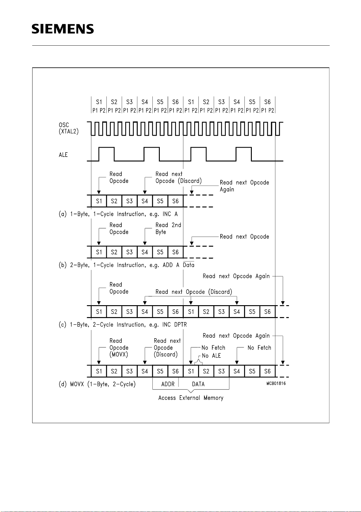
The diagrams in figure 2-7 show the fetch/execute timing related to the intern al states and phases .
Since these internal clock signals are not us er-accessible, the XTAL2 oscillato r signals and the ALE
(address latch enable) signal are s hown for external re ference. ALE is nor mally activated twice
during each machine cycle: once during S1P2 and S2P1, and again during S4P2 and S5P1.
Execution of a one-cycle instruction begins at S1P2, when the op-code is latched into the instruction
register. If it is a two-byte instruction, the second reading takes place during S4 of the same
machine cycle. If it is a one-byte instruction, there is still a fetch at S4, but the byte read (which would
be the next op-code) is ignored (discarded fetch), and the program counter is not incremented. In
any case, execution is completed at the end of S6P2.
Figures 2-7 (a) and (b) show the timing of a 1-byte, 1-cycle instruction and for a 2-byte, 1-cycle
instruction.
Most C501 instructions ar e executed in one cycle. MUL (multipl y) and DIV (divide) are the only
instructions that take more than two cycles to complete; they take four cycles. Normally two code
bytes are fetched from the program me mory during every machine cycle. The only except ion to this
is when a MOVX instruction is executed. MOVX is a one-byte, 2-cycle instruction that accesses
external data memory. During a MOVX, the two fetches in the second cycle are skipped while the
external data memory is being addressed and strobed. Figure 2-7 c) and d) show the timing for a
normal 1-byte, 2-cycle instruction and for a MOVX instruction.
Semiconductor Group 2-4
Page 21
Fundamental Structure
C501
Figure 2-7
Fetch Execute Sequence
Semiconductor Group 2-5
Page 22

Memory Organization
3 Memory Organization
The C501 CPU manipulates operands in the following four address spaces:
– up to 64 Kbyte of internal/external program memory
– up to 64 Kbyte of external data memory
– 256 bytes of internal data memory
– a 128 byte special function register area
Figure 3-1 illustrates the memory address spaces of the C501.
C501
External
Internal
"Code Space"
FFFF
2000
External
(EA = 0)(EA = 1)
H
H
1FFF
0000
FFFF
H
External
Indirect
Address
FF
H
Internal
RAM
80
H
H
0000
H
"Data Space" "Internal Data Space"
H
Internal
RAM
Direct
Address
Special
Function
Register
7F
H
00
H
MCD03224
FF
80
H
H
Figure 3-1
C501 Memory Map
Semiconductor Group 3-1
Page 23

Memory Organization
C501
3.1 Program Memory, “Code Space”
The C501-1R/-1E h as 8 Kbytes of read-only/OTP program memory, while the C501-L has no
internal program memory. The program memory can be externally expande d up to 64 Kbytes. If the
EA
pin is held high, the C501 executes out of internal program memory unl ess the address exceeds
1FFFH. Locations 2000H through FFFFH are then fetched from the external program memory. If
the EA
3.2 Data Memory, “Data Space”
The data memor y address space consists of an internal and an ext ernal memory space. The
internal data memory is divided into three physically separate and distinct blocks : the lower
128 bytes of RAM, the upper 128 bytes of RAM, and the 128 byte special function register (SFR)
area.
While the upper 128 bytes of data memory and the SFR area share the same address locations,
they are accessed through different addressing modes. The lower 128 bytes of data memory can
be accessed through direct or register indirec t addressing; the upper 128 bytes of RAM can be
accessed through register indirect addressing; the special function regis ters are accessible throug h
direct addressing. Four 8-register banks , each bank consisting of eight 8-bi t multi-purpose registers,
occupy locations 0 through 1FH in the lower RAM area. The next 16 bytes, locations 20H through
2FH, contain 128 directly addressable bit locations. The stack can be located anywhere in the
internal data memory address space, and the stack depth can be expanded up to 256 bytes.
pin is held low, the C501 fetches all instructions from the external program memory.
The external data memory can be expanded up to 64 Kbyte and can be accessed by instructions
that use a 16-bit or an 8-bit address.
3.3 General Purpose Registers
The lower 32 locations of the internal RAM are assigned to four banks with eight general purpose
registers (GPRs) each. Only one of these banks may be enabled at a time. Two bits i n the program
status word, RS0 and RS1, select the active register bank (see description of the PSW in
chapter 2). This allows fast context switching, which is useful when entering subroutines or
interrupt service routines.
The 8 general purpose regist ers of the selected register bank may be accessed by register
addressing. With register addressing the instruction op code indicates which register is to be used.
For indirect addressing R0 and R1 are used as pointer or index register to address internal or
external memory (e.g. MOV @R0).
Reset initializes the stack pointer to location 07H and increments it once to start from location 08
which is also the first register (R0) of register bank 1. Thus, if one is going to use more than one
register bank, the SP should be initialized to a different location of the RAM which is not used for
data storage.
H
Semiconductor Group 3-2
Page 24

Memory Organization
C501
3.4 Special Function Registers
All registers, except the p rogram counter an d the fou r general purpose regi ster bank s, resid e in th e
special function register area.
The 27 special function register (SFR) include pointers and registers that provide an interface
between the CPU and the other on-chip peripherals. There are also 128 directly addressable bits
within the SFR area.
All SFRs are listed in table 3-1 and table 3-2.
In table 3-2 they are organized in groups which refer to the functional blocks of the C50 1. Table 3-3
illustrates the contents (bits) of the SFRs.
Semiconductor Group 3-3
Page 25

Memory Organization
C501
Table 3-2
Special Function Registers - Functional Blocks
Block Symbol Name Address Contents after
Reset
1)
CPU ACC
B
DPH
DPL
PSW
SP
Interrupt
System
IE
IP
Ports P0
P1
P2
P3
Serial
Channel
PCON
SBUF
SCON
Timer 0 /
Timer 1
TCON
TH0
TH1
TL0
TL1
TMOD
Timer 2 T2CON
T2MOD
RC2H
RC2L
TH2
TL2
Pow. Sav.
PCON
Modes
Accumulator
B-Register
Data Pointer, High Byte
Data Pointer, Low Byte
Program Status Word Register
Stack Pointer
Interrupt Enable Register
Interrupt Priority Register
Port 0
Port 1
Port 2
Port 3
2)
Power Control Register
Serial Channel Buffer Register
Serial Channel Control Register
Timer 0/1 Control Register
Timer 0, High Byte
Timer 1, High Byte
Timer 0, Low Byte
Timer 1, Low Byte
Timer Mode Register
Timer 2 Control Register
Timer 2 Mode Register
Timer 2 Reload/Capture Register, High Byte
Timer 2 Reload/Capture Register, Low Byt
Timer 2 High Byte
Timer 2 Low Byte
2)
Power Control Register 87
E0
F0
83
82
D0
81
A8
B8
80
90
A0
B0
87
99
98
88
8C
8D
8A
8B
89
C8
C9
CB
CA
CD
CC
H
H
H
H
H
H
H
H
H
H
H
H
H
H
H
H
H
H
H
H
H
H
H
H
H
H
H
H
1)
1)
1)
1)
1)
1)
1)
1)
1)
1)
1)
00
H
00
H
00
H
00
H
00
H
07
H
0X000000
XX000000
FF
H
FF
H
FF
H
FF
H
0XXX0000
3)
XX
H
00
H
00
H
00
H
00
H
00
H
00
H
00
H
00
H
XXXXXXX0
00
H
00
H
00
H
00
H
0XXX0000
3)
B
3)
B
3)
B
3)
B
3)
B
1) Bit-addressable special f unc t ion registers
2) This special function register is listed repeatedly since some bits of it also belong to other functional blocks.
3) “X“ means that the value is undef ined and the location is reserved
Semiconductor Group 3-4
Page 26
Table 3-3
Contents of the SFRs, SFRs in numeric order of their addresses
Memory Organization
C501
Addr Register Content
after
Reset
2)
80
81
82
83
87
P0 FF
H
SP 07
H
DPL 00
H
DPH 00
H
PCON 0XXX-
H
0000
2)
88
89
TCON 00
H
TMOD 00
H
8AHTL0 00
8BHTL1 00
8CHTH0 00
8DHTH1 00
2)
90
98
99
A0
A8
P1 FF
H
2)
SCON 00
H
SBUF XX
H
2)
P2 FF
H
2)
IE 0X00-
H
0000
2)
B0
B8
P3 FF
H
2)
IP XX00-
H
0000
2)
C8
T2CON 00
H
1)
H
H
H
H
B
H
H
H
H
H
H
H
H
H
H
B
H
B
H
Bit 7 Bit 6 Bit 5 Bit 4 Bit 3 Bit 2 Bit 1 Bit 0
.7 .6 .5 .4 .3 .2 .1 .0
.7 .6 .5 .4 .3 .2 .1 .0
.7 .6 .5 .4 .3 .2 .1 .0
.7 .6 .5 .4 .3 .2 .1 .0
SMOD – – – GF1 GF0 PDE IDLE
TF1 TR1 TF0 TR0 IE1 IT1 IE0 IT0
GATE C/T
M1 M0 GATE C/T M1 M0
.7 .6 .5 .4 .3 .2 .1 .0
.7 .6 .5 .4 .3 .2 .1 .0
.7 .6 .5 .4 .3 .2 .1 .0
.7 .6 .5 .4 .3 .2 .1 .0
.7 .6 .5 .4 .3 .2 .1 .0
SM0 SM1 SM2 REN TB8 RB8 TI RI
.7 .6 .5 .4 .3 .2 .1 .0
.7 .6 .5 .4 .3 .2 .1 .0
EA – ET2 ES ET1 EX1 ET0 EX0
RD WR T1 T0 INT1 INT0 TxD RxD
– – PT2 PS PT1 PX1 PT0 PX0
TF2 EXF2 RCLK TCLK EXEN2 TR2 C/T2 CP/
RL2
C9HT2MOD XXXX-
XXX0
CAHRC2L 00
CBHRC2H 00
CCHTL2 00
CDHTH2 00
1) X means that the value is undefine d and the location is reserved
2) Bit-addressable special fun ction registers
H
H
H
H
–––––––DCEN
B
.7 .6 .5 .4 .3 .2 .1 .0
.7 .6 .5 .4 .3 .2 .1 .0
.7 .6 .5 .4 .3 .2 .1 .0
.7 .6 .5 .4 .3 .2 .1 .0
Semiconductor Group 3-5
Page 27

Memory Organization
Table 3-3
Contents of the SFRs, SFRs in numeric order of their addresses (cont’d)
C501
Addr Register Content
Bit 7 Bit 6 Bit 5 Bit 4 Bit 3 Bit 2 Bit 1 Bit 0
after
H
H
H
1)
CY AC F0 RS1 RS0 OV F1 P
.7 .6 .5 .4 .3 .2 .1 .0
.7 .6 .5 .4 .3 .2 .1 .0
Reset
2)
D0
E0
F0
1) X means that the value is undefine d and the location is reserved
2) Bit-addressable special fun ction registers
PSW 00
H
2)
ACC 00
H
2)
B 00
H
Semiconductor Group 3-6
Page 28

External Bus Interface
C501
4 External Bus Interface
The C501 allows for external memory expansion. To accomplish this, the external bus interface
common to most 8051-based controllers is employed.
4.1 Accessing External Memory
It is possible to distinguish between accesses to external program memory and external data
memory or other peripheral components respectively. This distinction is made by hardware:
accesses to external program memory use the signal PSEN
strobe. Accesses to external data memory use RD
functions of P3.7 and P3.6). Port 0 and port 2 (with exceptions) are used to provide data and
address signals. In this section only the port 0 and port 2 functions relevant to external memory
accesses are described.
Fetches from external program memory always use a 16-bit address. Accesses to external data
memory can use either a 16-bit address (MOVX @DPTR) or an 8-bit address (MOVX @Ri).
and WR to strobe the memory (alternate
(program store enable) as a read
4.1.1 Role of P0 and P2 as Data/Address Bus
When used for accessing external mem ory, p ort 0 p rovide s the data byte time-m ultip lexed with th e
low byte of the address. In this state, port 0 i s disconnected from its own port l atch, and the address/
data signal drives both FETs in the port 0 output buffers. Thus, in this appli cation, the port 0 pins are
not open-drain outputs and do not require external pullup resistors.
During any access to external me mory, the CPU wri tes FFH to the port 0 latch (the speci al functio n
register), thus obliterating whatever information the port 0 SFR may have been holding.
Whenever a 16-bit address is used, the high byte of the address comes out on port 2, where it is
held for the duration of the read or write cycle. During this time, the port 2 lines are disconnected
from the port 2 latch (the special function register).
Thus the port 2 latch does not have to contain 1s, and the contents of the port 2 SFR are not
modified.
If an 8-bit address is used (MOVX @Ri), the contents of the port 2 SFR remain at the port 2 pins
throughout the external memory cycle. This will facilitate paging. It should be noted that, if a port 2
pin outputs an address bit that is a 1, strong pullups will be used for the entire read/write cy cle and
not only for two oscillator periods.
Semiconductor Group 4-1
Page 29

External Bus Interface
C501
a)
ALE
PSEN
RD
P2
P0
b)
One Machine Cycle One Machine Cycle
S1 S2 S3 S4 S5 S6 S1 S2 S3 S4 S5 S6
INST.
IN
PCL
OUT
PCL OUT
valid
PCH
OUT
INST. INST. INST. INST.
IN OUT
PCL OUT
PCH PCH
OUT
PCL PCL
PCL OUT
valid
PCH
OUTIN IN OUT
valid
One Machine CycleOne Machine Cycle
PCL OUT
(A)
without
MOVX
OUTOUT
PCL
IN
valid
ALE
PSEN
RD
PCL
OUT
PCH
OUT
ININ
DPL or Ri
valid
P2
P0
INST. INST. INST.
PCL OUT
valid
Figure 4-1
External Program Memory Execution
DPH OUT OR
P2 OUT
DATA
IN
PCH
OUT
PCL
OUT
PCL OUT
valid
S6S5S4S3S2S1S6S5S4S3S2S1
(B)
with
MOVX
IN
MCT03220
Semiconductor Group 4-2
Page 30

External Bus Interface
C501
4.1.2 Timing
The timing of the external bus interface, in particular the relationship between the control signals
ALE, PSEN
, RD, WR and information on port 0 and port 2, is illustated in figure 4-1 a) and b).
Data memory
Program memory
4.1.3 External Program Memory Access
The external program memory is accessed under two conditions:
– whenever signal EA
– whenever the program counter (PC) contains a number that is larger than 1FFFH.
This requires the ROM-less version C501-L to have EA
bytes to be fetched from external memory.
When the CPU is executing out of exte rnal pro gram memory, all 8 bits of port 2 a re dedi cated to a n
output function and may not be used for general-purpose I/O. The contents of the port 2 SFR
however is not affected. During external program memory fetches port 2 lines output the high byte
of the PC, and during accesses to external data memory they output either DPH or the port 2 SFR
(depending on whether the external data memory access is a MOVX @DPTR or a MOVX @Ri).
When the C501 executes instructions from external program memory, port 2 is at all times
dedicated to output the high-order address byte. This means t hat port 0 and port 2 of the C501 ca n
never be used as general-purpose I/O. This means that port 0 and port 2 of the C501-L can never
be used as general-purpose I/O. This also applies to the C501-1R/1E when they are operating with
external program memory only.
: in a write cycle, the data byte to be written appears on port 0 just before WR is
activated and remains there until after WR
incoming byte is accepted at port 0 before the read strobe is deactivated.
: Signal PSEN functions as a read strobe.
is active (low) or
wired low to allow the lower 8 K program
is deactivated. In a read cycle, the
Semiconductor Group 4-3
Page 31

4.2 PSEN, Program Store Enable
External Bus Interface
C501
The read strobe for external fetches is PSEN
CPU is accessing external program memory, PSEN
MOVX instruction) no matter whether or not the byte fetched is actually needed for the current
instruction. When PSEN
including activation and deactivation of ALE and RD
cycle, including activation and deactivation of ALE and PSEN takes 3 oscillator periods. The
execution sequence for these two types of read cycles is shown in figure 4-1 a) and b).
4.3 ALE, Address Latch Enable
The main function of ALE is to provide a properly timed signal to latch the low byte of an address
from P0 into an external latch during fetches from external memory. The ad dress byte is valid at the
negative transition of ALE. For that purpose, ALE is activated twice every machine cycle. This
activation takes place even if the cycle involves no external fetch. The only time no ALE pulse
comes out is during an access to external data memory when RD
ALE of the second cycle of a MOVX instruction is missing (see figure 4-1 b). Consequently, in any
system that does not use data memory, ALE is activated at a constant rate of 1/6 of the oscillator
frequency and can be used for external clocking or timing purposes.
4.4 Overlapping External Data and Program Memory Spaces
In some applications it is desirable to execute a program from the same physical memory that is
used for storing data. In the C501 the e xternal p rogram and data memory spaces can be co mbined
by AND-ing PSEN
strobe that can be used for the combined physical memory. Since the PSEN
RD
cycle, the external memory needs to be fast enough to adapt to the PSEN cycle.
and RD. A positive logic AND of these two signals produces an active low read
is activated its timing is not the same as for RD. A complete RD cycle,
. PSEN is not activated for internal fetches. When the
is activated twice every cycle (except during a
, takes 6 oscillator periods. A complete PSEN
/WR signals are active. The first
cycle is faster than th e
Semiconductor Group 4-4
Page 32

External Bus Interface
C501
4.5 Enhanced Hooks Emulation Concept
The Enhanced Hooks Emulation Concept of the C500 microcontroller family is a new, innovative
way to control the execution of C500 MCUs and to gain extensive information on the internal
operation of the controllers. Emulation of on-chip ROM base d programs is possible, too (not true for
the C509-l, because it lacks internal program memory).
Each production chip has built-in logic for the supprt of the Enhanced Hooks Emulation Concept.
Therefore, no costly bond-out chips are necessary for emulation. This also ensure that emulation
and production chips are identical.
1)
The Enhanced Hooks Technology
together with an EH-IC to function similar to a bond-o ut chip. This simplifies th e design and reduces
costs of an ICE-system. ICE-systems using an EH-IC and a compatible C500 are able to emulate
all operating modes of the different versions of the C500 microcontrollers. This includes emulation
of ROM, ROM with code rollover and ROMless modes of operation. It is also able to operate in
single step mode and to read the SFRs after a break.
TM
, which requires embedded logic in the C500 allows the C500
SYSCON
PCON
TCON
RESET
EA
ALE
PSEN
RSYSCON
RPCON
RTCON
C500
MCU Interface Circuit
Optional
I/O Ports
Figure 4-2
Basic C500 MCU Enhanced Hooks Concept Configuration
Port 3 Port 1
Port 0
Port 2
Target System Interface
ICE-System Interface
to Emulation Hardware
EH-IC
Enhanced Hooks
RPort 0RPort 2
TEA TALE TPSEN
MCS02647
Port 0, port 2 and some of the control lines of the C500 based MCU are used by Enhanced Hooks
Emulation Concept to control the operation of the device during emulation and to transfer
informations about the programm execution and data transfer between the external emulation
hardware (ICE-system) and the C500 MCU.
1
“Enhanced Hooks Techno logy ” is a tra dem ark and patent of Metalink Corporation licensed to Siemens.
Semiconductor Group 4-5
Page 33

System Reset
C501
5 System Reset
5.1 Hardware Reset
The hardware reset function incorporated in the C501 allows for an easy automatic start-up at a
minimum of additional hardware and forces the controller to a predefined default state. The
hardware reset function can also be used during no rmal operation in order to restart the device. This
is particularly done when the power-down mode is to be terminated.
The RESET input is an active high input. An internal Schmitt trigger is used at the input for noise
rejection. Since the reset is synchronized internally, the RESET pin must be held high for at least
two machine cycles (24 osci llator perio ds) while th e oscil lator is running. With the osci llator runnin g
the internal reset is executed during the second machine cycle and is repeated every cycle until
RESET goes low again.
During reset, pins ALE and PSEN
are configured as inputs and should not be stimulated exte rnally.
An external stimulation at these lines during reset activates several test modes which are reserved
for test purposes. This in turn may cause unpredictable output operations at several port pins.
A pullup resistor is internally connected to
only. An automatic reset can be obtained when
V
to allow a power-up reset with an external capacitor
CC
V
is applied by connecting the RESET pin to V
CC
SS
via a capacitor. After VCC has been turned on, the capacitor must hold the voltage level at the
RESET pin for a specific time to effect a complete reset.
A correct reset leaves the processor in a defined state. The program execution starts at location
0000H. After reset is internally accomplished the port latches of ports 0, 1, 2 and 3 default in FFH.
This leaves port 0 floating, since it is an open drain port when not used as data/address bus. All
other I/O port lines (ports 1, 2 and 3) output at one (1).
The content of the internal RAM of the C501 is not affected by a reset. After power-up the content
is undefined, while it remains unchanged during a reset if the power supply is not turned off.
Semiconductor Group 5-1
Page 34

System Reset
C501
5.2 Hardware Reset Timing
This section describes the timing of the hardware reset signal.
The input pin RESET is sampled once during each machine c ycle. This happens in state 5 phase 2.
Thus, the external reset signal is synchronized to the internal CPU timing. When the reset is found
active (high level) the internal reset procedure is started. It needs two complete machine cycles to
put the complete device to its correct reset state, i.e. all special function registers contain their
default values, the port latches contain 1’s etc. The RESET signal must be active for at least two
machine cycles; after this time the C501 remains in its reset state as long as the signal is active.
When the signal goes inactive this transition is recognized in the following state 5 phase 2 of the
machine cycle. Then the proc essor sta rts its a ddress outp ut (when confi gured for ext ernal ROM) i n
the following state 5 phase 1. One phase later (state 5 phase 2) the first falling edge at pin ALE
occurs.
Figure 5-3 shows this timing for a configuration with EA = 0 (external program memory). Thus,
between the release of the RESET signal and the first falling edge at ALE there is a time period of
at least one machine cycle but less than two machine cycles.
S4 S5 S6 S1 S2 S3 S4 S5 S6 S1 S2 S3 S4 S5 S6 S1 S2
P1 P2
RESET
P0
P2
ALE
Figure 5-3
CPU Timing after Reset
One Machine Cycle
PCL
OUT
PCH
OUT
Inst.
PCL
in OUT
MCT02092
PCH
OUT
Semiconductor Group 5-2
Page 35

On-Chip Peripheral Components
C501
6 On-Chip Peripheral Components
I/O Ports
The C501 has four 8-bit I/O portst. Port 0 is an open-drain bidirectional I/O port, while ports 1 to 3
are quasi-bidirectional I/O ports with internal pullup resistors. That means, when configured as
inputs, ports 1 to 3 will be pulled high and wil l s ource current when extern ally pull ed l ow. Po rt 0 will
float when configured as input.
The output drivers of port 0 and 2 and the input buffers of po rt 0 are also used for acc essing external
memory. In this application, port 0 outputs the low byte of the external memory address, time
multiplexed with the byte being written or read. Port 2 outputs the hi gh byte of the e xternal memory
address when the address is 16 bits wide. Otherwis e, th e port 2 pins continue emitting the P2 SFR
contents. In this function, port 0 is not an open-drain port, but uses a strong internal pullup FET.
6.1 Parallel I/O
6.1.1 Port Structures
Digital I/O
The C501 allows for digital I/O on 32 lines grouped into 4 bidirectional 8-bit por ts. Each port bit
consists of a latch, an output driver and an input buffer. Read and write accesses to the I/O ports
P0 through P3 are performed via their corresponding special function registers P0 to P3.
Semiconductor Group 6-1
Page 36

On-Chip Peripheral Components
C501
Figure 6-1 shows a functional diagram of a ty pical bit latch and I/O buffer, which i s the core of eac h
of the 4 I/O-ports. The bit latch (one bit in the port’s SFR) is represented as a ty pe-D flip-flop, which
will clock in a value from the internal bus in res pons e to a “write-to-la tch” si gnal f rom the CPU. Th e
Q output of the flip-flop is placed on the internal bus in response to a “read-latch” signal from the
CPU. The level of the port pin itself is placed on the internal bus in response to a “read-pin” signal
from the CPU. Some instructions that read from a port (i.e. from the corresponding port SFR P0 to
P3) activate the “read-latch” signal, while others activate the “read-pin” signal.
Read
Latch
Int. Bus
Write
to
Latch
Read
Pin
Figure 6-4
Basic Structure of a Port Circuitry
D
CLK
Port
Latch
Q
Port
Q
Driver
Circuit
MCS01822
Port
Pin
Semiconductor Group 6-2
Page 37

On-Chip Peripheral Components
C501
Port 1, 2 and 3 output drivers have internal pullup FET’s (see figure 6-5). Each I/O line ca n be used
independently as an input or output. To be used as an input, the port bit stored in the bit latch must
contain a one (1) (that means for figure 6-5: Q=0), which turns off the output driver FET n1. Then,
for ports 1, 2 and 3, the pin is pulled hig h by the internal pul lups, but can be pul led low by an external
source. When externally pulled low the port pins source current (
ports are sometimes called “quasi-bidirectional”.
I
or ITL). For this reason these
IL
Read
Latch
Int. Bus
Write
to
Latch
Read
Pin
D
Bit
Latch
CLK
Figure 6-5
Basic Output Driver Circuit of Ports 1, 2, and 3
V
CC
Internal
Pull Up
Arrangement
Q
Q
n1
MCS01823
Pin
Semiconductor Group 6-3
Page 38

On-Chip Peripheral Components
C501
In fact, the pullups mentioned before and inclu ded in figure 6-5 are pullup arrangemen ts as shown
in figure 6-6. One n-channel pulldown FET and three pullup FETs are used:
V
CC
Port
Pin
MCS03230
Q
Input Data
(Read Pin)
=1
Delay = 1 State
_
<
1
p1 p2 p3
n1
V
SS
=1=1
Figure 6-6
Output Driver Circuit of Ports 1 to 5 and 7
–The pulldown FET n1 is of n-channel type. It is a very stron g driver transistor which is capabl e
of sinking high currents (
circuit to
V
must be avoided if the transisto r is turned on, since the high current might destroy
CC
I
); it is only activated if a “0” i s progra mmed to the port pin. A short
OL
the FET. This also means that no ”0“ must be programmed into the latch of a pin that is used
as input.
–The pullup FET p1 is of p-channel type. It is activated for two oscillator periods (S1P1 and
S1P2) if a 0-to-1 transition is programmed to the port pin, i.e. a “1” is programmed to the port
latch which contained a “0”. The extra pullup can drive a similar current as the pulldown FET
n1. This provides a fast transition of the logic levels at the pin.
–The pullup FET p2 is of p-channel type. It is always activated when a “1” is in the port latch,
thus providing the logic high outpu t lev el. Thi s p ullup FET sourc es a muc h lower c urrent tha n
p1; therefore the pin may also be tied to ground, e.g. when used as input with logic low input
level.
– The pullup FET p3 is of p-channel type. It is only activated if the voltage at the port pin is
higher than approximately 1.0 to 1.5 V. This provides an additional pullup current if a logic
high level shall be output at the pin (and the voltage is not forced lower than approximately
1.0 to 1.5 V). However, this transistor is turned off if the pin is driven to a logic low level, e.g
when used as input. In this configuration only the weak pullup FET p2 i s active, which s ources
the curr ent
(
I
). Thus, an additional power consumption can be avoided if port pins are used as inputs
TL
I
. If, in addition, the pullup FET p3 is activated, a higher current can be sourced
IL
with a low level applied. However, the driving capability is stronger if a logic high level is
output.
Semiconductor Group 6-4
Page 39

On-Chip Peripheral Components
C501
The described activating and deactivating of t he four different transistors results i n four states which
can be:
– input low state (IL), p2 active only
– input high state (IH) = steady output high state (SOH), p2 and p3 active
– forced output high state (FOH), p1, p2 and p3 active
– output low state (OL), n1 active
If a pin is used as input and a low level is applied, it will be in IL state, if a high level is applied, it
will switch to IH state. If the latch is loaded with “0”, the pin will be in OL state. If the latch holds a
“0” and is loaded with “1”, the pin will enter FOH state for two cycles a nd then s witch to SOH state.
If the latch holds a “1” and is reloaded with a “1” no state change will occur.
At the beginning of power-on reset the pins will be in IL state (latch is set to “1”, voltage level on
pin is below of the trip point of p3). Depending on the volta ge level and load applied to the pin, it will
remain in this state or will switch to IH (=SOH) state.
If it is is used as output, the weak pul l-up p2 will pull the voltage level at t he pin above p3’s tri p point
after some time and p3 will turn on and provide a strong “1”. Note, however, that if the load exceeds
the drive capability of p2 (
first 0-to-1 transition on the latch occurs. Until this the output level might stay below the trip point of
the external circuitry.
I
), the pin might remain in the IL state and provide a week “1” until the
IL
The same is true if a pin is used as bidirectional line a nd the external
circuitry is switched from
output to input when the pin is held at “0” and the load then exceeds the p2 drive capabilities.
I
If the load exceeds
the pin can be forced to “1” by writing a “0” followed by a “1” to the port pin.
IL
Semiconductor Group 6-5
Page 40

On-Chip Peripheral Components
C501
Port 0, in contrast to ports 1, 2 and 3, is considered as “true” bidirectional, because the port 0 pins
float when configured as inputs. Thus, this port differs in not having internal pullups. The pullup FET
in the P0 output driver (see figure 6-7) is used only when the port is emitting 1 s during the external
memory accesses. Otherwise, the pullup is always off. Consequently, P0 lines that are used as
output port lines are open drain lines. Writing a “1” to the port latch leaves both output FETs off and
the pin floats. In that condition it can be used as high-impedance input. If port 0 is configured as
general I/O port and has to emit logic high-level (1), external pullups are required.
Read
Latch
Int. Bus
Write
to
Latch
Read
Pin
Figure 6-7
Port 0 Circuitry
D
CLK
Bit
Latch
Addr./Data
Control
&
=1
Q
Q
MUX
V
CC
MCS02122
Port
Pin
Semiconductor Group 6-6
Page 41

On-Chip Peripheral Components
C501
6.1.1.1 Port 0 and Port 2 used as Address/Data Bus
As shown in figure 6-7 and below in figure 6-8, the output drivers of ports 0 and 2 can be switched
to an internal address or address/data bus for use in ex ternal memory acce sses. In this applicatio n
they cannot be used as general purpose I/O, even if not all address lines are used externally. The
switching is done by an internal control sign al dependent on the input level at the EA
contents of the program counter. If the ports are configured as an address/data bus, the port latches
are disconnected from the driver circuit. During this tim e, the P2 SFR remains unchanged while th e
P0 SFR has 1’s written to it . Being an address/data bus, port 0 uses a pullup FET as shown in
figure 6-7. When a 16-bit address is used, port 2 uses the additional strong pullups p1 to emit 1’s
for the entire external memory cycle instead of the weak ones (p2 and p 3) used during normal port
activity.
Read
Latch
Addr.
Control
V
CC
pin and/or the
Int. Bus
Write to
Latch
Read
Pin
Figure 6-8
Port 2 Circuitry
D
CLK
Bit
Latch
Internal
Pull Up
Arrangement
Q
MUX
Q
=1
MCS02123
Port
Pin
Semiconductor Group 6-7
Page 42

On-Chip Peripheral Components
C501
6.1.2 Alternate Functions
The pins of ports 1 and 3 are multifunction al. They are port pins and also serv e to implement special
features as listed in table 6-4.
Figure 6-9 shows a functional diagram of a port latch with alternate function. To pass the alternate
function to the output pin and vice versa, however, the gate between the latch and driver circuit must
be open. Thus, to use the alternate input or o utput fun ction s, the corresp onding bit l atch i n the p ort
SFR has to contain a one (1); otherwise the pulldown FET is on and the port pin is stuck at 0 . After
reset all port latches contain ones (1).
Read
Latch
Int. Bus
Write
to
Latch
Read
Pin
D
CLK
Bit
Latch
Q
Q
Alternate
Input
Function
Alternate
Output
Function
V
CC
Internal
Pull Up
Arrangement
Pin
&
MCS01827
Figure 6-9
Circuitry of Ports 1 and 3
Semiconductor Group 6-8
Page 43

On-Chip Peripheral Components
Ports 1 and 3 are provided for several alternate functions, as listed in table 6-4:
Table 6-4
Alternate Functions of Port 1 and 3
Port Pin Alternate Function
C501
P1.0
P1.1
P3.0
P3.1
P3.2
P3.3
P3.4
P3.5
P3.6
P3.7
T2
T2EX
RxD
TxD
INT0
INT1
T0
T1
WR
RD
Input to counter 2
Capture-reload trigger of timer 2 / up down count
Serial port’s receiver data input (asynchronous) or data input/output
(synchronous)
Serial port’s transmitter data output (asynchronous) or data clock output
(synchronous)
External interrupt 0 input, timer 0 gate control
External interrupt 1 input, timer 1 gate control
Timer 0 external counter input
Timer 1 external counter input
External data memory write strobe
External data momory read strobe
Semiconductor Group 6-9
Page 44

On-Chip Peripheral Components
C501
6.1.3 Port Handling
6.1.3.1 Port Timing
When executing an instruction that changes the value of a port latch, the new value arrives at the
latch during S6P2 of the final cycle of the instruction. However, port latches are only sampled by
their output buffers during phase 1 of any clock period (during phase 2 the output buffer holds the
value it noticed during the previous phase 1). Consequently, the new value in the port latch will n ot
appear at the output pin until the next phase 1, which will be at S1P1 of the next machine cycle.
When an instruction reads a val ue from a p ort pin (e.g. MOV A, P1 ) the port pi n is actuall y sample d
in state 5 phase 1 or phase 2 depending on port and alternate functions. Figure 6-10 illustrates this
port timing. lt must be noted that this mechanism of sampling once per machine cycle is also used
if a port pin is to detect an “edge”, e.g. when us ed as counter input. In this case an “edg e” is detected
when the sampled value differs from the value that was sampled the cycle before. Therefore, there
must be met certain requirements on the pulse le ngth of signals in order to a void signal “edges” not
being detected. The minimum time period of high and low level is one machine cycle, which
guarantees that this logic level is noticed by the port at least once.
Figure 6-10
Port Timing
XTAL2
Input sampled:
e.g. MOV A, P1
Port
S4 S5
P1 P2
Old Data
S6
P2P1
P2P1
S1
S2
P2P1
P2P1
P1 active for 1 State
(driver transistor)
New Data
S3
P2P1
MCT03231
Semiconductor Group 6-10
Page 45

On-Chip Peripheral Components
C501
6.1.3.2 Port Loading and Interfacing
The output buffers of ports 1, 2 and 3 can drive TTL inputs directly. The maximum port load which
still guarantees correct logic output levels can be looked up in the C501 DC characteristics in
chapter 10. The corresponding parameters are
The same applies to port 0 output buffers. They do, however, require external pullups to drive
floating inputs, except when being used as the address/data bus.
When used as inputs it must be noted that the ports 1, 2 and 3 are not floating but have internal
pullup transistors. The driving devices must be capable of sinking a sufficient current if a logic low
level shall be applied to the port pin (the parameters
specify these currents). Port 0 has floating inputs when used for digital input.
6.1.3.3 Read-Modify-Write Feature of Ports 1,2 and 3
Some port-reading instructions read the latch and othe rs read the pin. The i nstruc tions reading the
latch rather than the pin read a val ue, pos sib ly change it, and then rewrite it to the latch. These are
called “read-modify-write”- instructions, which are lis ted i n table 6-5. If t he de stinat ion is a port or a
port pin, these instructions read the latch rather than the pin. Note that all other instructions which
can be used to read a port, exclusively read the port pin. In any case, reading from latch or pin,
respectively, is performed by reading the SFR P0, P1, P2 and P3; for example, “MOV A, P3” reads
the value from port 3 pins, while “ANL P3, #0AAH” reads from the latch, modifies the value and
writes it back to the latch.
V
and VOH.
OL
I
and IIL in the C501 DC characteristics
TL
It is not obvious that the last three instructions in table 6-5 are read-modify-write instructions, but
they are. The reason is that they read the port byte, all 8 bits, modify the addressed bit, then write
the complete byte back to the latch.
Semiconductor Group 6-11
Page 46

On-Chip Peripheral Components
Table 6-5
Read-Modify-Write"- Instructions
Instruction Function
ANL Logic AND; e.g. ANL P1, A
ORL Logic OR; e.g. ORL P2, A
XRL Logic exclusive OR; e.g. XRL P3, A
JBC Jump if bit is set and clear bit; e.g. JBC P1.1, LABEL
CPL Complement bit; e.g. CPL P3.0
INC Increment byte; e.g. INC P1
DEC Decrement byte; e.g. DEC P1
DJNZ Decrement and jump if not zero; e.g. DJNZ P3, LABEL
MOV Px.y,C Move carry bit to bit y of port x
C501
CLR Px.y Clear bit y of port x
SETB Px.y Set bit y of port x
The reason why read-modify-write instructions a re directed to the latch rather than the pin is to avoid
a possible misinterpretation of the voltage level at the pin. For exam ple, a port bit might be use d to
drive the base of a transistor. When a “1” is written to the bi t, the transi stor is turned on. If th e CPU
then reads the same por t bit at the pin rather than the la tch, it will read the base voltage of the
transistor (approx. 0.7 V, i.e. a logic low level!) and interpret it as “0”. For example, when modi fying
a port bit by a SETB or CLR instruction, another bit in this port with the above mentioned
configuration might be changed if the value read from the pin were written back to the latch.
However, reading the latch rater than the pin will return the correct value of “1”.
Semiconductor Group 6-12
Page 47

On-Chip Peripheral Components
C501
6.2 Timers/Counters
The C501 contains three 16-bit timers/counters, timer 0, 1, and 2, which are useful in many
applications for timing and counting.
In “timer” function, the timer register is incremented every machine cycle. Thus one can think of it
as counting machine cycles. Since a machine cycle consists of 12 oscillator periods, the counter
rate is 1/12 of the oscillator frequency.
In “counter” function, the timer reg ister is incremented in response to a 1-to-0 tran sition (falling
edge) at its corresponding external input pin, T0, T1, or T2 (alternate functions of P3.4, P3.5 and
P1.0 resp.). In this function the external input i s sampled during S5P2 of every machine cycle. Whe n
the samples show a high in one cycle and a low in the next cycle, the count is incremented. The
new count value appears in the register during S3P1 of the cycle following the one in which the
transition was detected. Since it takes two machine cycles (24 oscillator periods) to recognize a 1to-0 transition, the maximum count rate is 124 of the oscillator frequency. There are no restrictions
on the duty cycle of the external input signal, but to ensure that a given level is sampled at least
once before it changes, it must be held for at least one full machine cycle.
Semiconductor Group 6-13
Page 48

On-Chip Peripheral Components
C501
6.2.1 Timer/Counter 0 and 1
Timer / counter 0 and 1 of the C501 are fully compatible with timer / counter 0 and 1 of the 80C51
and can be used in the same four operating modes:
Mode 0: 8-bit timer/counter with a divide-by-32 prescaler
Mode 1: 16-bit timer/counter
Mode 2: 8-bit timer/counter with 8-bit auto-reload
Mode 3: Tim er/cou nter 0 is co nfigur ed as one 8- bit tim er/c ounter and one 8-bit timer; Timer/
counter 1 in this mode holds its count. The effect is the same as setting TR1 = 0.
External inputs INT0
to facilitate pulse width measurements.
Each timer consists of two 8-bit registers (TH0 and TL0 for timer/counter 0, TH1 and TL1 for timer/
counter 1) whic h may be combined to one timer configuration depending on t he mode that is
established. The functions of the timers are controlled by two special function registers TCON and
TMOD.
In the following descriptions the symbols TH0 and TL0 are used to specify the high-byte and the
low-byte of timer 0 (TH1 and TL1 for ti mer 1, respectiv ely). The operating m odes are descri bed and
shown for timer 0. If not explicity noted, this applies also to timer 1.
and INT1 can be programmed to function as a gate for timer/count ers 0 and 1
Semiconductor Group 6-14
Page 49

On-Chip Peripheral Components
e
6.2.1.1 Timer/Counter 0 and 1 Registers
Totally six special function registers control the timer/counter 0 and 1 operation :
– TL0/TH0 and TL1/TH1 - counter registers, low and high part
– TCON and TMOD - control and mode select registers
C501
Special Function Register TL0 (Address 8AH) Reset Value : 00
Special Function Register TH0 (Address 8CH) Reset Value : 00
Special Function Register TL1 (Address 8BH) Reset Value : 00
Special Function Register TH1 (Address 8DH) Reset Value : 00
Bit No.
MSB LSB
76543210
H
H
H
H
.7 .6 .5 .48A
.7 .6 .5 .48C
.7 .6 .5 .48B
.7 .6 .5 .48D
.3 .2 .1 .0
TL0
TH0.3 .2 .1 .0
TL1.3 .2 .1 .0
TH1.3 .2 .1 .0
H
H
H
H
Bit Function
TLx.7-0
x=0-1
Timer/counter 0/1 low register
Operating Mode Description
0 “TLx” holds the 5-bit prescaler value.
1 “TLx” holds the lower 8-bit part of the 16-bit timer/coun ter value.
2 “TLx” holds the 8-bit timer/counter value.
3 TL0 holds the 8-bit timer/counter value; TL1 is not used.
THx.7-0
x=0-1
Timer/counter 0/1 high register
Operating Mode Description
0 “THx” holds the 8-bit timer/counter value.
1 “THx” holds the higher 8-bit part of the 16-bit timer/counter valu
2 “THx” holds the 8-bit reload value.
3 TH0 holds the 8-bit timer value; TH1 is not used.
Semiconductor Group 6-15
Page 50

On-Chip Peripheral Components
C501
Special Function Register TCON (Address 88H) Reset Value : 00
Bit No.
Bit Function
TR0 Timer 0 run control bit
TF0 Timer 0 overflow flag
TR1 Timer 1 run control bit
MSB LSB
76543210
8F
H
TF1 TR1 TF0 TR088
Set/cleared by software to turn timer/counter 0 ON/OFF.
Set by hardware on timer/counter overflow.
Cleared by hardware when processor vectors to interrupt routine.
Set/cleared by software to turn timer/counter 1 ON/OFF.
8E
H
The shaded bits are not used for controlling timer/counter 0 and 1.
H
8D
H
8C
8B
H
IE1 IT1 IE0 IT0
H
8A
H
89
H
88
H
TCON
H
TF1 Timer 1 overflow flag
Set by hardware on timer/counter overflow.
Cleared by hardware when processor vectors to interrupt routine.
Semiconductor Group 6-16
Page 51

On-Chip Peripheral Components
C501
Special Function Register TMOD (Address 89H) Reset Value : 00
Bit No.
MSB LSB
76543210
H
Gate C/T M1 M089
Gate C/T M1 M0
TMOD
Timer 1 Control Timer 0 Control
Bit Function
GATE Gating control
When set, timer/counter “x” is enabled only while “INT x” pin is high and “TRx”
control bit is set.
When cleared timer “x” is enabled whenever “TRx” control bit is set.
C/T
Counter or timer select bit
Set for counter operation (input from “Tx” input pin).
Cleared for timer operation (input from internal system clock).
M1
M0
Mode select bits
M1 M0 Function
H
0 0 8-bit timer/counter:
“THx” operates as 8-bit timer/counter
“TLx” serves as 5-bit prescaler
0 1 16-bit timer/counter.
“THx” and “TLx” are cascaded; there is no prescaler
1 0 8-bit auto-reload timer/counter.
“THx” holds a value which is to be reloaded into “TLx” each
time it overflows
1 1 Timer 0 :
TL0 is an 8-bit timer/counter controlled by the standard
timer 0 control bits. TH0 is an 8-bit timer only co ntrolled by
timer 1 control bits.
Timer 1 :
Timer/counter 1 stops
Semiconductor Group 6-17
Page 52

On-Chip Peripheral Components
C501
6.2.1.2 Mode 0
Putting either timer/counter 0,1 into mode 0 configures it as an 8-bit timer/c ounter with a div ide-by32 prescaler. Figure 6-11 shows the mode 0 operation.
In this mode, the timer register is configured as a 13-bit register. As the count rolls over from all 1’s
to all 0’s, it sets the timer overflow flag TF0. The overflow flag TF0 then can be used to request an
interrupt. The counted input is enabled to the timer when TR0 = 1 and either Gate = 0 or INT0
(setting Gate = 1 allows the timer to be controlled by external input INT0
, to facilitate pulse width
measurements). TR0 is a control bit in the special function register TCON; Gate is in TMOD.
The 13-bit register consists of all 8 bits of TH0 and the lower 5 bits of TL0. The upper 3 bits of TL0
are indeterminate and should be ignored. Setting the run flag (TR0) does not clear the registers.
Mode 0 operation is the same for timer 0 as for timer 1 . Substitute TR0, TF0, TH0, TL0 and INT0 for
the corresponding timer 1 signals in figure 6-11. There are two different gate bits, one for timer 1
(TMOD.7) and one for timer 0 (TMOD.3).
=1
÷ 12
C/T = 0
C/T = 1
TR0
_
<
1
&
MCS02143
P3.4/T0
Gate
P3.2/INTO
OSC
=1
Figure 6-11
Timer/Counter 0, Mode 0: 13-Bit Timer/Counter
Control
TL0 TH0
(5 Bits)
(8 Bits)
Interrupt
TF0
Semiconductor Group 6-18
Page 53

On-Chip Peripheral Components
C501
6.2.1.3 Mode 1
Mode 1 is the same as mode 0, except that the timer register is running with all 16 bits. Mode 1 is
shown in figure 6-12.
÷ 12
C/T = 0
C/T = 1
TR0
_
<
1
&
MCS02095
P3.4/T0
Gate
P3.2/INTO
OSC
=1
Figure 6-12
Timer/Counter 0, Mode 1: 16-Bit Timer/Counter
Control
TL0 TH0
(8 Bits)
(8 Bits)
Interrupt
TF0
Semiconductor Group 6-19
Page 54

On-Chip Peripheral Components
C501
6.2.1.4 Mode 2
Mode 2 configures the timer register as an 8-bit counter (TL0) with automatic reload, as shown in
figure 6-13. Overflow from TL0 not only sets TF0, but also reloads TL0 with the contents of TH0,
which is preset by software. The reload leaves TH0 unchanged.
Figure 6-13
Timer/Counter 0,1, Mode 2: 8-Bit Timer/Counter with Auto-Reload
Semiconductor Group 6-20
Page 55

On-Chip Peripheral Components
C501
6.2.1.5 Mode 3
Mode 3 has different effects on timer 0 and timer 1. Timer 1 in mode 3 simply holds its count. The
effect is the same as setting TR1=0. Timer 0 in mode 3 establishes TL0 and TH0 as two seperate
counters. The logic for mode 3 on timer 0 is shown in figure 6-14. TL0 uses the timer 0 control bits:
C/T
, Gate, TR0, INT0 and TF0. TH0 is locked into a timer function (counting machine cycles) and
takes over the use of TR1 and TF1 from timer 1. Thus, TH0 now controls the “timer 1” interrupt.
Mode 3 is provided fo r applications requiri ng an extra 8-bit timer o r counter. When timer 0 is in
mode 3, timer 1 can be turned on and off by switching it out of and into its own mode 3, or can still
be used by the serial channel as a baud rate generator, or in fact, in any application not requiring
an interrupt from timer 1 itself.
P3.4/T0
Gate
P3.2/INT0
/12
f
OSC
TR1
OSC
=1
÷ 12
f
/12
OSC
C/T = 0
TL0
(8 Bits)
C/T = 1
Control
TR1
_
<
1
&
TH0
(8 Bits)
Control
TF0
TF1
Interrupt
Interrupt
MCS02096
Figure 6-14
Timer/Counter 0, Mode 3: Two 8-Bit Timers/Counters
Semiconductor Group 6-21
Page 56

On-Chip Peripheral Components
C501
6.2.2 Timer/Counter 2
Timer 2 is a 16-bit timer / counter which can operate as timer or counter. It has three operating
modes:
– 16-bit auto-reload mode (up or down counting)
– 16-bit capture mode
– Baudrate generator for the serial interface
The modes are selected by bits in the SFR T2CON (C8H) as shown in table 6-6:
Table 6-6
Timer/Counter 2 - Operating Modes
RXCLK + TXCLK CP/RL2
0 0 1 16-bit auto-reload
0 1 1 16-bit capture
1 X 1 Baud rate generator
X X 0 (OFF)
Timer 2 consists of two 8-bit registers, TH2 and TL2. In the timer function, the TL2 register is
incremented every machine cycle. Since a machine cycle consists of 12 oscillator periods, the count
rate is 1/12 of the oscillator frequency.
In the counter function, the register is incremented in response to a 1-to-0 transition at its
corresponding external input pin, T2 (P1.0). In this function, the external input is sampled during
S5P2 of every machine cycle. When the samples show a high in one cycle and a low in the next
cycle, the count is incremented. The new value appears in the register during S3P1 of the cycle
following the one in which the transition was detected. Since it takes two machine cycles to
recognize a 1-to-0 transition, the maximum count rate is 1/24 of the oscilllator freque ncy. To ensure
that a given level is sampled at least once before it changes, it should be held for at least one full
machine cycle.
TR2 Mode
Semiconductor Group 6-22
Page 57

On-Chip Peripheral Components
6.2.2.1 Timer 2 Registers
Totally six special function registers control the timer/counter 2 operation :
– TL2/TH2 and RC2L/RC2H - counter and reload/capture registers, low and high part
– T2CON and T2MOD - control and mode select registers
C501
Special Function Register TL2 (Address CCH) Reset Value : 00
Special Function Register TH2 (Address CDH) Reset Value : 00
Special Function Register RC2L (Address CAH) Reset Value : 00
Special Function Register RC2H (Address CBH) Reset Value : 00
Bit No.
MSB LSB
76543210
H
H
H
H
.7 .6 .5 .4CC
MSB.6.5.4CD
.7 .6 .5 .4CA
MSB.6.5.4CB
.3 .2 .1 LSB
TL2
TH2.3 .2 .1 .0
RC2L.3 .2 .1 LSB
RC2H.3 .2 .1 .0
H
H
H
H
Bit Function
TL2.7-0 Timer 2 value low byte
The TL2 register holds the 8-bit low part of the 16-bit timer 2 count value.
TH2.7-0 Timer 2 value high byte
The TH2 register holds the 8-bit high part of the 16-bit timer 2 count value.
RC2L.7-0 Reload register low byte
CRCL is the 8-bit low byte of the 16-bit reload register of timer 2.
RC2H.7-0 Reload register high byte
CRCH is the 8-bit high byte of the 16-bit reload register of timer 2.
Semiconductor Group 6-23
Page 58

On-Chip Peripheral Components
C501
Special Function Register T2CON (Address C8H) Reset Value : 00
MSB
Bit No. CF
H
TF2 EXF2 RCLK TCLKC8
CE
H
CD
H
CC
H
CB
H
CA
H
C9
H
LSB
H
C8
H
T2CONEXEN2 TR2 C/T2 CP/RL2
Bit Function
TF2 Timer 2 Overflow Flag.
Set by a timer 2 overflow. Must be cleared by software. TF2 will not be s et wh en
either RCLK = 1 or TCLK = 1.
EXF2 Timer 2 External Flag.
Set when either a capture or reload is caused by a negative transition on T2EX
and EXEN2 = 1. When timer 2 interrupt is enabled, EXF2 = 1 will cause the CPU
to vector to the timer 2 interrupt routine. EXF2 must be cleared by software. EXF2
does not cause an interrupt in up/down counter mode (DCEN = 1, SFR T2MOD)
RCLK Receive Clock Enable.
When set, causes the serial port to use timer 2 overflow pulses for its receive
clock in serial port modes 1 and 3. RCLK = 0 causes timer 1 overflows to be used
for the receive clock.
H
TCLK Transmit Clock Enable.
When set, causes the serial port to use timer 2 overflow pulses for its transmit
clock in serial port modes 1 and 3 . TCL K = 0 causes timer 1 overflow to be used
for the transmit clock.
EXEN2 Timer 2 External Enable.
When set, allows a capture or reload to occur as a result of a negative transition
on pin T2EX (P1.1) if timer 2 is not being used to clock the serial port. EXEN2 = 0
causes timer 2 to ignore events at T2EX.
TR2 Start / Stop Control for Timer 2.
TR2 = 1 starts timer 2.
C/T2
Timer or Counter Select for Timer 2.
C/T2
= 0 for timer function. C/T2 = 1 for external event counter (falling edge
triggered).
CP/RL2
Capture /Reload Select.
CP/RL2
EXEN2 = 1. CP/RL2
= 1 causes captures to occur an negative transitions at pin T2EX if
= 0 causes automatic reloads to occur when timer 2
overflows or negative transitions occur at pin T2EX when EXEN2 = 1. When
either RCLK = 1 or TCLK = 1, this bit is ignored and the timer is forced to autoreload on timer 2 overflow.
Semiconductor Group 6-24
Page 59

On-Chip Peripheral Components
C501
Special Function Register T2MOD (Address C9H) Reset Value : XXXXXXX0
Bit No.
Bit Function
– Not implemented, reserved for future use.
DCEN Down Counter Enable
MSB LSB
76543210
H
––––C9
The shaded bits are not used for controlling timer 2.
When set, this bit allows timer 2 to be configured as an up/down counter.
– – – DCEN
T2MOD
B
Semiconductor Group 6-25
Page 60

On-Chip Peripheral Components
C501
6.2.2.2 Auto-Reload (Up or Down Counter)
Timer 2 can be programmed to count up or down when configured in its 16-bit auto-reload mode.
This feature is invoked by a bit named DCEN (Down Counter Enable, SFR T2MOD, 0C9H). When
DCEN is set, timer 2 can count up or down depending on the value of pin T2EX (P1.1).
Figure 6-15 shows timer 2 automatically counting up when DCEN = 0. In this mode there are two
options selectable by bit EXEN2 in SFR T2CON.
Figure 6-15
Timer 2 Auto-Reload Mode (DCEN = 0)
If EXEN2 = 0, timer 2 counts up to FFFFH and then sets the TF2 bit upon overflow. The overflow
also causes the timer registers to be relo aded with the 16-bit value in RC2H and RC2L. The v alues
in RC2H and RC2L are preset by software.
If EXEN2 = 1, a 16-bit reload can be triggered either by an overflow or by a 1-to-0 transition at the
external input T2EX (P1.1). This transition also sets the EXF2 bit. Both the TF2 and EXF2 bits can
generate an timer 2 interrupt if enabled.
Setting the DCEN bit enables timer 2 to count up or down as shown i n figure 6-16. In thi s mode the
T2EX pin controls the direction of count.
Semiconductor Group 6-26
Page 61

On-Chip Peripheral Components
C501
Figure 6-16
Timer 2 Auto-Reload Mode (DCEN = 1)
A logic 1 at T2EX makes timer 2 count up. The timer will overflow at FFFFH and set the TF2 bit.
This overflow also causes the 16-bit value in RC2H and RC2L to be reloaded into the timer
registers, TH2 and TL2, respectively.
A logic 0 at T2EX makes timer 2 count down. Now the timer underflows when TH2 and TL2 equal
the values stored in RC2H and RC2L. The underflow sets the TF2 bit and causes FFFFH to be
reloaded into the timer registers. The EXF2 bit toggles whenever timer 2 overflows or underflows.
This bit can be used as a 17th bit of resolution if desired. In this operating mode, EXF2 does not
flag an interrupt.
Note: P1.1/T2EX is sampled during S5P2 of every machine cycle. The next increment/decrement
of timer 2 will be done during S3P1 in the next cycle.
Semiconductor Group 6-27
Page 62

On-Chip Peripheral Components
C501
6.2.2.3 Capture
In the capture mode there are two options selected by bit EXEN2 in SFR T2CON.
If EXEN2 = 0, timer 2 is a 16-bit timer or counter which upon overflow sets bit TF2 in SFR T2CON.
This bit can be used to generate an interrupt.
If EXEN2 = 1, timer 2 still does the above, but with added feature that a 1-to-0 transi tion at external
input T2EX causes th e current value in TH2 and TL2 to be cap tured into RC2H and RC2L,
respectively. In addition, the transition at T2EX cause s bit EXF2 in SFR T2CON to be set. The EXF2
bit, like TF2, can generate an interrupt. The capture mode is illustrated in figure 6-17.
Figure 6-17
Timer 2 in Capture Mode
The baud rate generator mode is selected by RCLK = 1 and/or TCLK = 1 in SFR T2CON. It will be
described in conjunction with the serial port.
Semiconductor Group 6-28
Page 63

On-Chip Peripheral Components
C501
6.3 Serial Interface
The serial port is full duplex, mean ing i t can transmi t and re ceive si multaneously. It is also receivebuffered, meaning it can commence reception of a second byte before a previously received byte
has been read from the receive register. (However, if th e first byte stil l hasn’t b een read by th e time
reception of the second byte is complete, one of the bytes will be lost). The serial port receive and
transmit registers are both accessed at special function register SBUF. Writing to SBUF loads the
transmit register, and reading SBUF accesses a physically separate receive register.
The serial port can operate in 4 modes (one synchronous mode, three asynchronous modes):
Mode 0, Shift Register (Synchronous) Mode:
Serial data enters and exits through RxD. TxD outputs the shift clock. 8 data bits are transmitted/
received: (LSB first). The baud rate is fixed at
more detailed information)
Mode 1, 8-Bit USART, Variable Baud Rate:
1
/12 of the oscillator frequency. (See section 6.3.4 for
10 bits are transmitted (through TxD) or received (thro ugh RxD): a start bit (0), 8 data bits (LSB first),
and a stop bit (1). On receive, the stop bit goes into RB8 in special function register SCON. The
baud rate is variable. (See section 6.3.5 for more detailed information)
Mode 2, 9-Bit USART, Fixed Baud Rate:
11 bits are transmitted (through TxD) or received (thro ugh RxD): a start bit (0), 8 data bits (LSB first),
a programmable 9th data bit, and a st op bit (1). O n transmit, the 9th data b it (TB8 in SCON) can b e
assigned to the value of 0 or 1. Or, for example, the parity bit (P, in the PSW) could be moved into
TB8. On receive, the 9th data bit goes into RB8 in special function register SCON, while the stop
bit is ignored. The baud rate is programmable to either
1
/32 or 1/64 of the oscillator frequency. (See
section 6.3.6 for more detailed information)
Mode 3, 9-Bit USART, Variable Baud Rate:
11 bits are transmitted (through TxD) or received (thro ugh RxD): a start bit (0), 8 data bits (LSB first),
a programmable 9th data bit, and a stop bit (1). In fact, mode 3 is the same as mode 2 in all respects
except the baud rate. The baud rate in mode 3 is var iable.(See section 6.3.6 for more detaile d
information)
In all four modes, transmission is initiated by any instruction that us es SBUF as a destination
register. Reception is initiated in mode 0 by the c ondition RI = 0 and REN = 1. Reception is in itiated
in the other modes by the incomming start bit if REN = 1.
The serial interface also provides interrupt requests when transmission or reception of a frames
have been completed. The corresponding interrupt request flags are TI or RI, resp. See chapter 7
of this user manual for more details about the interrupt structure. The interrupt request flags TI and
RI can also be used for polling the serial interface, if the s erial i nterrupt is not to be u sed (i.e . serial
interrupt not enabled).
Semiconductor Group 6-29
Page 64

On-Chip Peripheral Components
C501
6.3.1 Multiprocessor Communications
Modes 2 and 3 have a special provision for multiprocess or communications. In these modes, 9 data
bits are received. The 9th one goes i nto RB8. Then com es a stop b it. The port can be p rogramme d
such that when the stop bit is received, the serial port interrupt will be activated only if RB8 = 1. This
feature is enabled by setting bi t SM2 in SCON. A way to use thi s feature i n multiprocesso r systems
is as follows.
When the master processor wants to trans mit a block o f da ta to one of se veral slaves, it first sends
out an address byte which identifies the target slave. An address byte differs from a data byte in
that the 9th bit is 1 in an address byte and 0 in a data byte. With SM2 = 1, no slave will be interrupted
by a data byte. An address byte, however, will interrupt all slaves, so that each slave can examine
the received byte and see if it is beeing addressed. The addressed slave will clear its SM2 bit and
prepare to receive the data bytes that will be coming. The sl aves that weren’t being address ed leave
their SM2s set and go on about their business, ignoring the incoming data bytes.
SM2 has no effect in mode 0, and in mode 1 can be used to check the validity of the stop bit. In a
mode 1 reception, if SM2 = 1, the receive interrupt will not be activated unless a valid stop bit is
received.
6.3.2 Serial Port Registers
The serial port control and st atus register is the special function re gister SCON. This register
contains not only the mode selection bits, but also the 9th data bit for transmit and receive TB8 and
RB8), and the serial port interrupt bits (TI and RI).
SBUF is the receive and transmit buffer of serial interface. Writing to SBUF loads the transmit
register and initiates transmission. Reading out SBUF accesses a physically separate receive
register.
Semiconductor Group 6-30
Page 65

On-Chip Peripheral Components
C501
Special Function Register SCON (Address 98H) R eset Value : 00
Special Function Register SBUF (Address 99H) Reset Value : XX
Bit No. MSB LSB
H
9F
SM0 SM1 SM2 REN98
H
9E
H
9D
H
9C
H
9B
H
9A
H
TB8 RB8 TI RI
99
H
98
H
SCON
76543210
99
H
Serial Interface Buffer Register
SBUF
Bit Function
SM0
SM1
Serial port 0 operating mode selection bits
SM0 SM1 Selected operating mode
f
0 0 Serial mode 0 : Shift register, fixed baud rate (
OSC
/6)
0 1 Serial mode 1 : 8-bit UART, variable baud rate
1 0 Serial mode 2 : 9-bit UART, fixed baud rate (
f
OSC
/16 or f
OSC
/32)
1 1 Serial mode 3 : 9-bit UART, variable baud rate
H
H
SM2 Enable serial port multiprocessor communication in modes 2 and 3
In mode 2 or 3, if SM2 is set to 1 then RI will not be activated if the received 9th
data bit (RB8) is 0. In mode 1, if SM2 = 1 then RI will not be activated if a valid
stop bit was not received. In mode 0, SM2 should be 0.
REN Enable receiver of serial port
Enables serial reception. Set by software to enable serial reception. Cleared by
software to disable serial reception.
TB8 Serial port transmitter bit 9
TB8 is the 9th data bit that will be transmitted in modes 2 and 3. Set or cleared by
software as desired.
RB8 Serial port receiver bit 9
In modes 2 and 3, RB8 is the 9th data bit that was received. In mode 1, if SM2 = 0,
RB8 is the stop bit that was received. In mode 0, RB8 is not used.
TI Serial port transmitter interrupt flag
TI is set by hardware at the end of the 8th bi t time in mode 0, or at the beginning
of the stop bit in the other modes, in any serial transmission. TI must be cleared
by software.
RI Serial port receiver interrupt flag
RI is set by hardware at the end of the 8th bi t time in mode 0, or halfway through
the stop bit time in the other mode s, in a ny serial reception (exception see SM2).
RI must be cleared by software.
Semiconductor Group 6-31
Page 66

On-Chip Peripheral Components
C501
6.3.3 Baud Rates Generation
There are several possibilities to generate the baud rate clock for the serial port depending on the
mode in which it is operating.
For clarification some terms regarding the difference between “baud rate clock” and “baud ra te”
should be mentioned. The serial interface requires a clock rate which is 16 times the baud rate for
internal synchronization. Therefore, the baud rate generators have to prov ide a “baud rate clock” to
the serial interface which - there divided by 16 - results in the actual “baud rate”. However, all
formulas given in the following section already include the factor and calculate the final baud rate.
Further, the abrevation
operation).
The baud rate of the serial port is controlled by bit SMOD which is located in the special function
register PCON as shown below.
f
refers to the external clock frequency (oscillator or external input clock
OSC
Special Function Register PCON (Address 87H) Reset Value : 0XXX0000
Bit No. MSB LSB
76543210
H
SMOD–––87
GF1 GF0 PDE IDLE
PCON
The shaded bits are not used for controlling the baud rate.
Bit Function
SMOD Double baud rate
When set, the baud rate of serial interface in modes 1, 2, 3 is doubled. After rese t
this bit is cleared.
Mode 0
The baud rate in mode 0 is fixed:
f
Mode 0 baud rate = oscillator frequency/12 =
OSC
/12
Mode 2
B
The baud rate in mode 2 depends on the value of bit SMOD in special function register PCON. If
SMOD = 0 (which is the value on reset), the baud rate is
f
/64. If SMOD = 1, the baud rate is f
OSC
OSC
32.
Mode 2 baud rate = 2
/64×(f
OSC
)
SMOD
Modes 1 and 3
The baud rates in mode 1 and 3 are determined by the timer overflow rate. These baud rates can
be determined by timer 1 or by timer 2 or by both (one for transmit and the other for receive).
Semiconductor Group 6-32
/
Page 67

On-Chip Peripheral Components
C501
6.3.3.1 Using Timer 1 to Generate Baud Rates
When timer 1 is used as the baud rate generator, the baud rates in modes 1 and 3 are determined
by the timer 1 overflow rate and the value of SMOD as follows:
Modes 1,3 baud rate = 2
The timer 1 interrupt should be disabled in this application. The timer itself can be configured for
either “timer” or “counter” operation, and in any of its 3 running modes. In the most typical
applications, it is configured for “timer” operation, in the auto-reload mode (high nib ble of
TMOD=0010B). In that case, the baud rate is given by the formula
Modes 1,3 baud rate = 2
One can achieve very low b aud rates with timer 1 by lea ving the timer 1 interrupt enab led, and
configuring the timer to run as a 16-bit timer (high nibble of TMOD = 0001B), and using the timer 1
interrupt to do a 16-bit software reload.
Table 6-7 lists commonly used baud rates and how they can be obtained from timer 1.
SMOD
/32×(timer 1 overflow rate)
SMOD
/32×f
/ [12×(256–TH1)]
OSC
Table 6-7
Timer 1 Generated Commonly Used Baud Rates
Baud Rate
Mode 0 max:1 MHz
Mode 2 max:375 K
Modes 1, 3: 62.5 K
19.2 K
9.6 K
4.8 K
2.4 K
1.2 K
110
110
f
OSC
12 MHz
12 MHz
12 MHz
11.059 MHz
11.059 MHz
11.059 MHz
11.059 MHz
11.059 MHz
6MHz
12 MHz
SMOD Timer 1
C/T Mode Reload
X
1
1
1
0
0
0
0
0
0
X
X
0
0
0
0
0
0
0
0
X
X
2
2
2
2
2
2
2
1
Value
X
X
FF
H
FD
H
FD
H
FA
H
F4
H
E8
H
72
H
FEEB
H
Semiconductor Group 6-33
Page 68

On-Chip Peripheral Components
C501
6.3.3.2 Using Timer 2 to Generate Baud Rates
Timer 2 is selected as the baud rate generator by setting TCLK and/or RCLK in T2CON. Note the n
the baud rates for transmit and receive can be simultaneousl y different. Setting RCLK a nd/or TCLK
puts timer 2 into its baud rate generator mode, as shown in figure 6-18.
Figure 6-18
Timer 2 in Baud Rate Generator Mode
The baud rate generator mode is similar to the auto-reload mode, in that rollover in TH2 cau ses the
timer 2 registers to be reloaded with the 16-bit value in registers RC2H and RC2L, which are preset
by software.
Now the baud rates in modes 1 and 3 are determined by timer 2’s overflow rate as follows:
Modes 1, 3 baud rate = timer 2 overflow rate/16
Semiconductor Group 6-34
Page 69

On-Chip Peripheral Components
C501
The timer can be configured for either “timer” or “counter” operation: In the most typical app lications,
it is configured for “timer” operation (C/T2
it’s being used as a baud rate generator. Normally, as a timer it would increment every machine
cycle (thus at
f
/12). As a baud rate generator, however, it increments e very state time ( f
OSC
that case the baud rate is given by the formula
f
Modes 1,3 baud rate =
/32×[65536 – (RC2H, RC2L)]
OSC
where (RC2H, RC2L) is the content of RC2H and RC2L taken as a 16-bit unsigned integer.
Note that the rollover in TH2 does not set TF2, and will not generate an interrupt. Therefore, the
timer 2 interrupt does not have to be disabl ed when timer 2 is in the baud rate gene rator mode. Note
too, that if EXEN2 is set, a 1-to-0 transition in T2EX can be used as an extra external interrupt, if
desired.
It should be noted that when timer 2 is running (TR2 = 1) in “timer” function in the baud rate
generator mode, one should not try to read or write TH2 or TL2. Under these conditions the timer
is being incremented every state time, and the results of a read or write may not be accurate. The
RC registers may be read, but shouldn’t be written to, because a write might overlap a reload and
cause write and/or reload errors. Turn the timer off (clear TR2) before accessing the timer 2 or RC
registers, in this case.
= 0). “Timer” operation is a little different for timer 2 when
/2). In
OSC
Semiconductor Group 6-35
Page 70

On-Chip Peripheral Components
C501
6.3.4 Details about Mode 0
Serial data enters and exists through RxD. TxD outputs the shift clock. 8 data bits are transmitted/
received: (LSB first). The baud rate is fixed at
Figure 6-19 shows a simplyfied functional diagram of the serial po rt in mode 0. The associated
timing is illustrated in figure 6-20.
Transmission is initiated by any instruction that uses SBUF as a destination register. The “Write to
SBUF” signal at S6P2 also loads a 1 into the 9th position of the transmit shift register and tells the
TX control block to commence a transmission . The internal timing is such that one full machine
cycle will elapse between “Write to SBUF”, and activation of SEND.
SEND enables the output of the shift register to the alternate output function line of P3.0, and also
enables SHIFT CLOCK to the alternate output function line of P3.1. SHIFT CLOCK is low during
S3, S4, and S5 of every machine cycle, and high du ri ng S6, S1 and S2. At S6P2 of every m achin e
cycle in which SEND is active, the contents of the transmit shift register are shifted to the right one
position.
f
OSC
/12.
As data bits shift out to the right, zeroes come in from the left. When the MSB of the data byte is at
the output position of the shift register, then the 1 that was initialy loaded i nto the 9th position, is jus t
to the left of the MSB, and all positions to the left of that contain zeroes. This condition fla gs the TX
control block to do one last shift and then deactivate SEND and set TI. Both of these actions occ ur
at S1P1 of the 10th machine cycle after “Write to SBUF”.
Reception is initiated by the cond ition REN = 1 and R1 = 0 . At S6P2 of the next machine cycle, the
RX control unit writes the bits 1111 1110 to the receive shift register, and in the next clock phase
activates RECEIVE.
RECEIVE enables SHIFT CLOCK to the alternate output function line of P3.1. SHIFT CLOCK
makes transitions at S3P1 and S6P1 of every machine cycle. At S6P2 of every machine cycle in
which RECEIVE is active, the contents of the receive shift register are shi fted to the left one position.
The value that comes in from the right is the value that was sampled at the P3.0 pin at S5P2 of the
same machine cycle.
As data bit comes in from the right, 1s shift out to the left. When the 0 that was initially loaded into
the rightmost position arrives at the left most position in the shift regis ter, it flags the RX control block
to do one last shift and load SBUF. At S1P1 of the 10th machine cycle after the write to SCON that
cleared RI, RECEIVE is cleared and RI is set.
Semiconductor Group 6-36
Page 71

Write
to
SBUF
On-Chip Peripheral Components
C501
Internal Bus
1
S
D
Q
SBUF
&
RXD
P3.0 Alt.
Output
Function
REN
RI
CLK
Baud
Rate
Clock
&
S6
Start
TX Clock
Serial
Port
Interrupt
Start
RX Clock
Load
SBUF
Zero Detector
TX Control
TI
_
<
1
RI
RX Control
Input Shift Register
Shift
Send
Receive
Shift
01 111111
Shift
Shift
_
<
1
Shift
Clock
RXD
P3.0 Alt.
Input
Function
&
TXD
P3.1 Alt.
Output
Function
SBUF
Read
SBUF
Internal Bus
Figure 6-19
Serial Interface, Mode 0, Functional Diagram
Semiconductor Group 6-37
MCS02101
Page 72

S
S
S
S
S
S
S
S
S
S S
S
S
S
S
S S
S
S
S
S
S S
S
S
S
S
S S
S
S
S
S
S S
S
S
S
S
S S
S
S
S
S
S S
S
S
S
S
S S
S S
S
S
S
S
S
6
5
4
3
21
6
5
4
3
21
6
5
4
3
21
6
5
4
3
21
6
5
4
3
21
6
5
4
3
21
6
5
4
3
21
6
5
4
3
21
6
5
4
3
21
6
5
4
3
12
S6P2
D7
D5 D6
D4
D3
D1 D2
D0
On-Chip Peripheral Components
C501
ReceiveTransmit
MCT02102
S5P
D0 D1 D2 D3 D4 D5 D6 D7
S3P1 S6P1
Write to SCON (Clear RI)
ALE Write to SBUF
Send
Shift
RXD (Data Out)
TXD (Shift Clock)
Figure 6-20
Serial Interface, Mode 0, Timing Diagram
Semiconductor Group 6-38
TI
ReceiveRIRXD (Data In)
Shift
TXD (Shift Clock)
Page 73

On-Chip Peripheral Components
C501
6.3.5 Details about Mode 1
Ten bits are transmitted (through TxD), or received (through RxD): a start bit (0), 8 data bits (LSB
first), and a st op bit (1). On receive, th e stop bit goes into RB8 i n SCON. The baud rate is
determined either by the timer 1 overflow rate, or the timer 2 overflow rate, or both (one for transmi t
and the other for receive).
Figure 6-21 shows a simplified functional diagram of the seria l port in mode 1. The assiociated
timings for transmit receive are illustrated in figure 6-22.
Transmission is initiated by an instruction that uses SBUF as a destination register. The “Write to
SBUF” signal also loads a 1 into the 9th bit position of the transmit shift register and flags the TX
control unit that a transmission is requested. Transmission starts at the next rollover in the divideby-16 counter. (Thus, the bit times are synchronized to the divide-by-16 counter, not to the “Write
to SBUF” signal).
The transmission begins with activation of SEND
DATA is activated, which enables the output bit of the transmit shift register to TxD. The first shift
pulse occurs one bit time after that.
As data bits shift out to the right, zeroes are cloc ked in from th e left. When the MSB of the dat a byte
is at the output position of the shift register, then the 1 that was initially loaded into the 9th position
is just to the left of the MSB, and all positions to the left of that contain zeroes. This condition flags
the TX control unit to do one last shift and then dea ctivate SEND
divide-by-16 rollover after “Write to SBUF”.
Reception is initiated by a detected 1-to-0 transition at RxD. For this purpose RxD is sampled at a
rate of 16 times whatever baud rate has been established. When a transition is detected, the divideby-16 counter is immediately reset, and 1FFH is written into the input shift register, and reception
of the rest of the frame will proceed.
The 16 states of the counter divide each bit time into 16ths. At the 7th, 8th and 9th counter states
of each bit time, the bit detector samples the value of RxD. The value acce pted is the value that was
seen in at latest 2 of the 3 samples. This is done for the noise rejection. If the value accepted durin g
the first bit time is not 0, the receive circuits are reset and the unit goes back to looking for another
1-to-0 transition. This is to provide rejection or false start bits. If the start bit proves valid, it is shifted
into the input shift register, and reception of the rest of the frame will proceed.
As data bits come in from the right, 1s shift out to the left. When the start bit arrives at the leftmost
position in the shift register, (which in mode 1 is a 9-bit register), it flags the RX control block to do
one last shift, load SBUF and RB8, and set RI. The signal to l oad SBUF and RB8, and to set RI, will
be generated if, and only if, the following conditions are met at the time the final shift pulse is
generated.
, which puts the start bit at TxD. One bit time later,
and set TI. This occurs at the 10th
1) RI = 0, and
2) Either SM2 = 0, or the received stop bit = 1
If either of these two condtions is not met, the received frame is irretrievabl y los t. If both condi tions
are met, the stop bit goes into RB8, the 8 data bit goes into SBUF, and RI is ac tiva ted. At this time,
whether the above conditions are met or not, the unit goes back to looking for a 1-to-0 transition in
RxD.
Semiconductor Group 6-39
Page 74

Write
to
SBUF
On-Chip Peripheral Components
C501
Internal Bus
1
S
D
Q
SBUF
&
_
<
TXD
1
Baud
Rate
Clock
RXD
Sample
1-to-0
Transition
Detector
CLK
÷ 16
Start
TX Clock
Interrupt
÷ 16
Start
Bit
Detector
Zero Detector
TX Control
Serial
Port
RX
RX Control
Load
SBUF
Shift
_
<
1
Input Shift Register
TI
RI
1FF
H
(9Bits)
Data
Send
Load
SBUF
Shift
Shift
Read
SBUF
Internal Bus
Figure 6-21
Serial Interface, Mode 1, Functional Diagram
Semiconductor Group 6-40
SBUF
MCS02103
Page 75

Transmit
On-Chip Peripheral Components
C501
Stop Bit
D7
D6
D5
D4
Stop Bit
D7
D5 D6
D4
D3
MCT02104
D3
D2D1
D0
S1P1
to SBUF
Clock
Write
Send
Data
Shift
TX
Start Bit
TXD
Figure 6-22
Serial Interface, Mode 1, Timing Diagram
TI
÷ 16 Reset
ClockRXRXD
D1 D2
D0
Start Bit
Receive
Sample Times
Bit Detector
Shift
RI
Semiconductor Group 6-41
Page 76

On-Chip Peripheral Components
C501
6.3.6 Details about Modes 2 and 3
Eleven bits are transmitted (through TxD), or received (through RxD): a s tart bit (0), 8 data bits (LSB
first), a programmable 9th data bit, and a stop bit (1). On transmit, the 9th data bit (TB8) can be
assigned the value of 0 or 1. On receive, the 9th data bit goes into RB8 in SCON. The baud rate is
programmable to either 1/32 or 1/64 the oscillator frequency in mode 2 (When bit SMOD in SFR
PCON (87H) is set, the baud rate is
either timer 1 or 2 depending on the state of TCLK and RCLK (SFR T2CON).
Figure 6-23 shows a functional diagram of the serial port in modes 2 and 3. The receive portion is
exactly the same as in mode 1. The transmit portion differs from mode 1 only in the 9th bit of the
transmit shift register. The associated timings for transmit/receive are illustrated in figure 6-24.
Transmission is initiated by any instruction that uses SBUF as a destination register. The “Write to
SBUF” signal also loads TB8 into the 9th bit position of the transmit shift register and flags the TX
control unit that a transmission is requested. Transmission starts at the next rollover in the divideby-16 counter. (Thus, the bit times are synchronized to the divide-by-16 counter, not to the “Write
to SBUF” signal.)
f
/32). Mode 3 may have a variable baud rate generated from
OSC
The transmision begins with activation of SEND, which puts the start bit at TxD. One bit time later,
DATA is activated, which enables the output bit of the transmit shift register to TxD. The first shift
pulse occurs one bit time after that. The first shift clocks a 1 (the stop bit) into the 9th bit position of
the shift register. Thereafter, only zeroes are clocked in. Thus, as data bits shift out to the right,
zeroes are clocked in from the left. Whe n TB8 i s at the ou tput pos itio n of the shift register, then the
stop bit is just to the left of TB8, and all positions to the left of that contain zeroes. This conditon
flags the TX control unit to do one last shift and then deactivate SEND and set TI. This occurs at
the 11th divide-by-16 rollover after “Write to SBUF”.
Reception is initiated by a detected 1-to-0 transition at RxD. For this purpose RxD is sampled at a
rate of 16 times whatever baud rate has been established. When a transition is detected, the divideby-16 counter is immediately reset, and 1FFH is written to the input shift register.
At the 7th, 8th and 9th counter states of each bit time, the bit detector samples the value of RxD.
The value accepted is the value that was seen in at least 2 of the 3 samples. If the value accepted
during the first bit time is not 0, the receive circuits are reset and the unit goes back to looking for
another 1-to-0 transition. If the start bit proves valid, it is shifted into the input shift register, and
reception of the rest of the frame will proceed.
As data bit come from the right, 1s shift out to the left . When the start bit arr ives at the leftmost
position in the shift register (which in modes 2 and 3 is a 9-bit re gister), it flags the RX control block
to do one last shift, load SBUF and RB8, and to set RI. The signal to load SBUF and RB8, and to
set RI, will be generated if, and only if, the following conditions are met at the time the final shift
pulse is generated:
1) RI = 0, and
2) Either SM2 = 0 or the received 9th data bit = 1
If either of these conditions is not met, the received frame is irretrievably lost, and RI is not set. If
both conditions are met, the received 9th data bit goes into RB8, and the first 8 data bit goes into
SBUF. One bit time later, whether the above conditions were met or not, the unit goes back to
looking for a 1-to-0 transition at the RxDTxD input.
Note that the value of the received stop bit is irrelevant to SBUF, RB8 or RI.
Semiconductor Group 6-42
Page 77

Write
to
SBUF
On-Chip Peripheral Components
C501
Internal Bus
TB8
S
D
Q
SBUF
&
_
TXD
<
1
Baud
Rate
Clock
RXD
Sample
1-to-0
Transition
Detector
CLK
÷ 16
Stop Bit
Start
Generation
TX Clock
Interrupt
÷ 16
RX Clock
Start
Bit
Detector
Zero Detector
TX Control
Serial
Port
RX Control
Load
SBUF
Shift
_
<
1
Input Shift Register
Data
Send
TI
RI Load
SBUF
Shift
1FF
(9Bits)
Shift
Read
SBUF
Internal Bus
Figure 6-23
Serial Interface, Mode 2 and 3, Functional Diagram
Semiconductor Group 6-43
SBUF
MCS02105
Page 78

Transmit
On-Chip Peripheral Components
C501
Stop Bit
TB8
D7
D6D5
D4
Stop Bit
RB8
D7
D5 D6
D4
D3
MCT02587
D3
D2D1
D0
Mode 2 : S6P1
Mode 3 : S1P1
Start Bit
Write to SBUF
TX Clock
Send
Data
Shift
TXD
TI
Figure 6-24
Serial Interface, Mode 2 and 3, Timing Diagram
÷ 16 Reset
Stop Bit Gen.
D1 D2
D0
RX Clock
Start Bit
RX
Bit Detector
Receive
Sample Times
Shift
RI
Semiconductor Group 6-44
Page 79

Interrupt System
C501
7 Interrupt System
The C501 provides 6 interrupt sources with two priority lev els . Four i nterrupts can be generated by
the on-chip peripherals (timer 0, timer 1, timer 2 and serial interface), and two interrupts may be
triggered externally (P3.2/INT0
This chapter shows the interrupt structure, the interrupt vectors and the interrupt related special
function registers. Figure 7-25 gives a general overview of the interrupt sources and illustrate the
request and the control flags which are described in the next sections.
and P3.3/INT1).
P1.1/
T2EX
Timer 0 Overflow
Timer 1 Overflow
Timer 2 Overflow
EXEN2
T2CON.3
USART
TCON.0
TF2
T2CON.7
EXF2
T2CON.6
RI
SCON.0
TI
SCON.1
TF0
TCON.5
TF1
TCON.7
_
<
1
_
<
1
ET0
IE.1 IP.1
ET1
IE.3
ET2
IE.5 IP.5
ES
PT0
PT1
IP.3
PT2
PS
IP.4IE.4
High Priority
Low Priority
P3.2/
INT0
IT0
TCON.0
P3.3/
INT1
IT1
TCON.2
IE0
TCON.1
EX0
IE.0 IP.0
IE1
TCON.3
Figure 7-25
Interrupt Structure
Semiconductor Group 7-1
PX0
EX1
IE.2 IP.2
EA
IE.7
PX1
MCS01783
Page 80

Interrupt System
C501
7.1 Interrupt Registers
7.1.1 Interrupt Enable Register
Each interrupt vector can be individually enabled or disabled by setting or clearing the
corresponding bit in the interrupt enable register IE (interrupt enable) or T2CON. This register also
contains the global disable bit (EA), which can be cleared to disable all interrupts at once. Gen erally,
after reset all interrupt enable bits are set to 0. That means that the corresponding interrupts are
disabled.
Special Function Register IE (Address A8H) Reset Value : 0X000000
MSB
Bit No. AF
A8
H
The shaded bit is not used for interru pt co nt rol.
EA – ET2 ES
AE
H
AD
H
AC
H
AB
H
AA
H
A9
H
ET1 EX1 ET0 EX0
LSB
A8
H
H
IE
Bit Function
EA Enable/disable all interrupts.
If EAL=0, no interrupt will be acknowledged.
If EAL=1, each interrupt source is individually enabled or disabled by setting or
clearing its enable bit.
– Not implemented. Reserved for future use.
ET2 Timer 2 overflow / external reload interrupt enable.
If ET2 = 0, the timer 2 interrupt is disabled.
If ET2 = 1, the timer 2 interrupt is enabled.
ES Serial channel (USART) interrupt enable
If ES = 0, the serial channel interrupt 0 is disabled.
If ES = 1, the serial channel interrupt 0 is enabled.
B
ET1 Timer 1 overflow interrupt enable.
If ET1 = 0, the timer 1 interrupt is disabled.
If ET1 = 1, the timer 1 interrupt is enabled.
EX1 External interrupt 1 enable.
If EX1 = 0, the external interrupt 1 is disabled.
If EX1 = 1, the external interrupt 1 is enabled.
ET0 Timer 0 overflow interrupt enable.
If ET0 = 0, the timer 0 interrupt is disabled.
If ET0 = 1, the timer 0 interrupt is enabled.
EX0 External interrupt 0 enable.
If EX0 = 0, the external interrupt 0 is disabled.
If EX0 = 1, the external interrupt 0 is disabled.
Semiconductor Group 7-2
Page 81

Interrupt System
C501
Special Function Register T2CON (Address C8H) Reset Value : 00
LSB
C8
H
H
T2CONEXEN2 TR2 C/T2 CP/RL2
Bit No. CF
MSB
CE
H
H
TF2 EXF2 RCLK TCLKC8
The shaded bits are not used for int errupt enable control.
CD
H
CC
H
CB
H
CA
H
C9
H
Bit Function
EXEN2 Timer 2 External Enable.
When set, allows a capture or reload to occur as a result of a negat ive transition on
pin T2EX (P1.1) if timer 2 is not being used to clock the serial port. EXEN2 = 0
causes timer 2 to ignore events at T2EX.
H
Semiconductor Group 7-3
Page 82

7.1.2 Interrupt Request / Control Flags
Interrupt System
C501
The external interrupts 0 and 1 (INT0
and INT1) can each be either level-activated or negative
transition-activated, depending on bits IT0 and IT1 in register TCON. The flags that actually
generate these interrupts are bits IE0 and lE1 in TCON. When an external interrupt is generated, the
flag that generated this interrupt is cleared by the hard ware when the service routine is vectored too,
but only if the interrupt was transition-activated. lf the interrupt was level-activated, then the
requesting external source directly controls the request flag, rather than the on-chip hardware.
The timer 0 and timer 1 interrupts are generated b y TF0 and TF1 in register TCON, which are set
by a rollover in their respective timer/counter registers. When a timer interrupt is generated, the flag
that generated it is cleared by the on-chip hardware when the service routine is vectored too.
Special Function Register TCON (Address 88H) Reset Value : 00
LSB
H
88
H
TCON
Bit No. 8F
88
MSB
8E
H
H
TF1 TR1 TF0 TR0
The shaded bits are not used for int errupt control.
8D
H
8C
H
H
8B
8A
H
89
H
IE1 IT1 IE0 IT0
H
Bit Function
TF1 Timer 1 overflow flag
Set by hardware on timer/counter 1 overflow. Cleared by hardware when
processor vectors to interrupt routine.
TF0 Timer 0 overflow flag
Set by hardware on timer/counter 0 overflow. Cleared by hardware when
processor vectors to interrupt routine.
IE1 External interrupt 1 request flag
Set by hardware when external interrupt 1 edge is detected. Cleared by hardware
when processor vectors to interrupt routine.
IT1 External interrupt 1 level/edge trigger control flag
If IT1 = 0, low level triggered external interrupt 1 is selected.
If IT1 = 1, falling edge triggered external interrupt 1 is selected.
IE0 External interrupt 0 request flag
Set by hardware when external interrupt 0 edge is detected. Cleared by hardware
when processor vectors to interrupt routine.
IT0 External interrupt 0 level/edge trigger control flag
If IT0 = 0, low level triggered external interrupt 0 is selected.
If IT0 = 1, falling edge triggered external interrupt 0 is selected.
Semiconductor Group 7-4
Page 83

Interrupt System
C501
The timer 2 interrupt is generated by the logical OR of bit TF2 and EXF2 in register T2CON.
Neither of these flags is cleared by hardware when the service routine is vectored to. In fact, the
service routine may have to determi ne whether it was TF2 or EXF2 tha t generated the interrupt, and
the bit will have to be cleared by software.
The serial port interrupt is generated by a logical OR of flag RI and TI in SFR SCON. Neither of
these flags is cleared by hardware when the service routine is vectored too. In fact, the service
routine will normally have to determi ne whether i t was th e rece ive interrupt flag o r the tran smis sio n
interrupt flag that generated the interrupt, and the bit will have to be cleared by software.
Special Function Register T2CON (Address C8H) Reset Value : 00
Special Function Register SCON (Address. 98H) Reset Value : 00
LSB
C8
H
H
T2CONEXEN2 TR2 C/T2 CP/RL2
H
98
H
SCON
Bit No. CF
Bit No. 9F
98
MSB
CE
H
H
H
TF2 EXF2 RCLK TCLKC8
9E
H
SM0 SM1 SM2 REN
The shaded bits are not used for int errupt request control.
CD
H
9D
H
H
CC
H
9C
H
CB
H
9B
H
TB8 RB8 TI RI
CA
H
9A
C9
H
99
H
Bit Function
TF2 Timer 2 Overflow Flag.
Set by a timer 2 overflow. Must be cleared by software. TF2 will not be set when
either RCLK = 1 or TCLK = 1.
EXF2 Timer 2 External Flag.
Set when either a capture or reload is caused by a negative transition on T2EX and
EXEN2 = 1. When timer 2 interrupt is enabled, EXF2 = 1 will cause the CPU to
vector to the timer 2 interrupt routine. EXF2 must be cleared by software. EXF2
does not cause an interrupt in up/down counter mode (DCEN = 1, SFR T2MOD)
H
H
TI Serial interface transmitter interrupt flag
Set by hardware at the end of a serial data transmission. Must be cleared by
software.
RI Serial interface receiver interrupt flag
Set by hardware if a serial data byte has been received. Must be cleared by
software.
Semiconductor Group 7-5
Page 84

Interrupt System
C501
7.1.3 Interrupt Priority Register
Each interrupt source can also be individually programmed to one of two priority le vels by setting or
clearing a bit in the SFR IP (Interrupt Priority, 0: low priority, 1: high priority).
Special Function Register IP (Address B8H) Reset Value : XX000000
MSB
Bit No.76543210
B8
H
Bit Function
– Not implemented. Reserved for future use.
PT2 Timer 2 Interrupt Priority Level.
PS Serial Channel Interrupt Priority Level.
PT1 Timer 1 Overflow Interrupt Priority Level.
PX1 External Interrupt 1 Priority Level.
– – PT2 PS
The shaded bits are not used for int errupt control.
If PT2 = 0, the Timer 2 interrupt has a low priority.
If PS = 0, the Serial Channel interrupt has a low priority.
If PT1 = 0, the Timer 1 interrupt has a low priority.
If PX1 = 0, the external interrupt 1 has a low priority.
PT1 PX1 PT0 PX0
LSB
IP
B
PT0 Timer 0 Overflow Interrupt Priority Level.
If PT0 = 0, the Timer 0 interrupt has a low priority.
PX0 External Interrupt 0 Priority Level.
If PX0 = 0, the external interrupt 0 has a low priority.
Semiconductor Group 7-6
Page 85

Interrupt System
C501
7.2 Interrupt Priority Level Structure
A low-priority interrupt can itself be interrupted by a high-priority interrupt, but not by another lowpriority interrupt. A high-priority interrupt cannot be interrupted by any other interrupt source.
If two requests of different priority level a re received simultaneously, the request of higher priority is
serviced. If requests of the same priority ar e recei ved simul taneous ly, an internal polling sequence
determines which request is serviced. Thus within each priority level there is a second priority
structure determined by the polling sequence as shown in table 7-8 below:
Table 7-8
Priority-within-Level Structure
Interrupt Source Priority
External Interrupt 0, IE0
Timer 0 Interrupt, TF0
External Interrupt 1, IE1
Timer 1 Interrupt, TF1
Serial Channel, RI or TI
Timer 2 Interrupt, TF2 or EXF2
High
↓
Low
Semiconductor Group 7-7
Page 86

Interrupt System
C501
7.3 How Interrupts are Handled
The interrupt flags are sampled at S5P2 in each machine cycle. The sampled flags are polled during
the following machine cycle. If one of the flags was in a set condition at S5P2 of the preceeding
cycle, the polling cycle will f ind it and the interrupt s ystem will generate a LCALL to the appropriate
service routine, provided this hardware-generated LCALL is not blocked by any of the following
conditions:
1. An interrupt of equal or higher priority is already in progress.
2. The current (polling) cycle is not in the final cycle of the instruction in progress.
3. The instruction in progress is RETI or any write access to registers IE or IP.
Any of these three conditions will block the generation of the LCALL to the interrup t service routine.
Condition 2 ensures that the instruction in progress is completed before vectoring to any service
routine. Condition 3 ensures that if the instruction in progress is RETI or any write access to
registers IE or IP, then at least one more instruction will be executed before any interrupt i s vectored
too; this delay guarantees that changes of the interrupt status can be observed by the CPU.
The polling cycle is repeated with each machine cycle, and the values polled are the values that
were present at S5P2 of the previous machine cycle. Note that if any interrupt flag is active but not
being responded to for one of the conditions already mentioned, or if the flag is no longer active
when the blocking conditio n is removed, the denied interrupt will not be servic ed. In other words, the
fact that the interrupt flag was once active but not serviced is not remembered. Every polling cycle
interrogates only the pending interrupt requests.
The polling cycle/LCALL sequence is illustrated in figure 7-26.
C2C1 C3 C4 C5
S5P2
Interrupt
is latched
Interrupts
are polled
Long Call to Interrupt
Vector Address
Figure 7-26
Interrupt Response Timing Diagram
Interrupt
Routine
MCT01859
Semiconductor Group 7-8
Page 87

Interrupt System
C501
Note that if an interrupt of a higher priority level goes active prior to S5P2 in the machine cycle
labeled C3 in figure 7-26 then, in accordance with the above rules, it will be vectored to during C5
and C6 without any instruction for the lower priority routine to be executed.
Thus, the processor acknowledges an interrupt req uest by executing a hardware-generated LCAL L
to the appropriate servicing routine. In some cases it also clears the flag that generated the
interrupt, while in other cases it does not; then this has to be done by the user’s software. The
hardware clears the external interrupt flags IE0 and IE1 only if they were transition-activated. The
hardware-generated LCALL pushes the contents of the program counter onto the stack (but it does
not save the PSW) and reloads the program counter with an address that depends on the source of
the interrupt being vectored too, as shown in the following table 7-9.
Table 7-9
Interrupt Source and Vectors
Interrupt Source Interrupt Vector Address Interrupt Request Flags
External Interrupt 0 0003
Timer 0 Overflow 000B
External Interrupt 1 0013
Timer 1 Overflow 001B
Serial Channel 0023
Timer 2 Overflow / Ext. Reload 002B
Execution proceeds from that location until the RETI instruction is encountered. The RETI
instruction informs the processor that the interrupt routine is no longer in progress, then pops the
two top bytes from the stack and reloads the program counter. Execution of the interrupted program
continues from the point where it was stopped. Note that the RETI instruction is very important
because it informs the processor that the program left the current interrupt priority level. A simple
RET instruction would also have returned execution to the interrupted program, but it would have
left the interrupt control system thinking an interrupt was sti ll in progress. In this case no interrupt of
the same or lower priority level would be acknowledged.
H
H
H
H
H
H
IE0
TF0
IE1
TF1
RI / TI
TF2 / EXF2
Semiconductor Group 7-9
Page 88

Interrupt System
C501
7.4 External Interrupts
The external interrupts 0 and 1 can be programmed to be level-activated or negative-transition
activated by setting or clearing bit IT0, respecti vely in register TCON. If ITx = 0 (x = 0 or 1), external
interrupt x is triggered by a detected low level at the INTx
negative edge-triggered. In this mode, if successive samples of the INTx
cycle and a low in the next cycle, interrupt request flag IEx in TCON is set. Flag bit IEx=1 then
requests the interrupt.
If the external interrupt 0 or 1 is level-activated, the external source has to hold the request active
until the requested interrupt is actually generated. Then it has to deactivate the request before the
interrupt service routine is completed, or else another interrupt will be generated.
The external timer 2 reload trigger interrupt request flag EXF2 will be activated by a negative
transition at pin P1.1/T2EX but only if bit EXEN2 is set.
Since the external interrupt pins are sampled once in each machine cycle, an input high or low
should be held for at least 6 oscillator periods to ensure sampling. lf the external interrupt is
transition-activated, the external source has to hold the request pin high for at least one cycle, and
then hold it low for at least one cycle to ensure that the transition is recognized so that the
corresponding interrupt request flag will be set (see figure 7-27). The external interrupt request
flags will automatically be cleared by the CPU when the service routine is called.
pin. If ITx = 1, external interrupt x is
pin show a high in one
Figure 7-27
External Interrupt Detection
Semiconductor Group 7-10
Page 89

Interrupt System
C501
7.5 Interrupt Response Time
If an external interrupt is recog nized, its correspon ding request flag is set at S5P2 in eve ry machine
cycle. The value is not po lled by the circuitry until the next machine cycl e. If the request is activ e and
conditions are right for it to be acknowledged, a hardware subroutine call to the requested service
routine will be next instruction to be executed. The call itself takes two cycles. Thus a minimum of
three complete machine cycles will e lapse between activation and external interrupt request and the
beginning of execution of the first instruction of the service routine.
A longer response time would be obtained if the request was blocked by one of the three previously
listed conditions. If an interrupt of equal or higer priority is already in progress, the additional wait
time obviously depends on the nature of the other interrupt’s service routine. If the instruction in
progress is not in its final cycle, the additional wait time cannot be more than 3 cycles since the
longest instructions (MUL and DIV) are only 4 cycles long; and , if the instruction in progress is RETI
or a write access to registers IE or IP the additional wait time cannot be more than 5 cycles (a
maximum of one more cycle to complete the instruction in progress, plus 4 cycles to complete the
next instruction, if the instruction is MUL or DIV).
Thus a single interrupt system, the response time is always more than 3 cycles and less than
9 cycles.
Semiconductor Group 7-11
Page 90

Power Saving Modes
C501
8 Power Saving Modes
The C501 provides two basic power saving modes :
– Idle mode
– Power down mode.
8.1 Power Saving Mode Control Register
The two power saving modes are controlled by bits which are located in the special function
registers PCON. The SFR PCON is located at SFR address 87H.
The bits PDE and IDLE in SFR PCON select the power down mode or the idle mode, respectively.
If the power down mode and the idle mode are set at the same time, power down takes precedence.
Furthermore, register PCON contains two general purpose flags. For example, the flag bits GF0
and GF1 can be used to give an indication if an interrupt occurred during normal operation or during
an idle. Then an instruction that activates idle can also set one or both flag bits. When idle is
terminated by an interrupt, the interrupt service routine can examine the flag bits.
Special Function Register PCON (Address 87H) Reset Value : 0XXX0000
Bit No.
Symbol Function
– Reserved for future use
GF1 General purpose flag
GF0 General purpose flag
PDE Power down enable bit
IDLE Idle mode enable bit
87
MSB
76543210
SMOD – – – GF1 GF0 PDE IDLE
H
The function of the shaded bit is not used for power saving mode control.
When set, starting of the power down mode is enabled
When set, starting of the idle mode is enabled
LSB
PCON
B
Semiconductor Group 8-1
Page 91

Power Saving Modes
C501
8.2 Idle Mode
In the idle mode the oscillator of the C501 conti nues to run, but the CPU is gated off from the clock
signal. However, the interrupt system, the serial port, and all timers are further provided with the
clock. The CPU status is preserved in its entirety: the stack pointer, program counter, program
status word, accumulator, and all other registers maintain their data during idle mode.
The reduction of power consumption, which can be ach ieved by this feature depends on the num ber
of peripherals running. If all timers are stopped and the serial interfaces are not running, the
maximum power reduction can be achieved. This state is also the test condition for the idle mode
I
.
CC
So, the user has to take care which peripheral sho uld c ontinue to run an d whi ch ha s to be stoppe d
during idle mode. Also the state of all port pins – either the pins controlled by their latches or
controlled by their secondary functions – depends on the status of th e controller when enteri ng idle
mode.
Normally, the port pins hold the logical state the y had at the time when the idle mode was activate d.
If some pins are programmed to se rve as a lternate func tions they still continue to output during idl e
mode if the assigned function is on. This applies to the serial interface in case it cannot finish
reception or transmission during normal operation. The control signals ALE and PSEN
logic high levels.
are hold at
As in normal operation mode, the ports can be used as inputs during idle mode. Thus a capture or
reload operation can be triggered, the timers can be used to count external events, and external
interrupts will be detected.
The idle mode is a useful feat ure whic h m akes it poss ibl e to "freeze" the proces sor's sta t us - eit her
for a predefined time, or until an external event reverts the controller to normal operation, as
discussed below. The watchdog timer is the only peripheral which is automatically stopped during
idle mode.
The idle mode is entered by setting the flag bit IDLE (PCON.0).
Note:
PCON is not a bit-addressable register, so the above mentioned sequence for entering the idle
mode is obtained by byte-handling instructions, as shown in the following example:
ORL PCON,#00000001B ;Set bit IDLE
The instruction that sets bit IDLE is the last instruction executed before going into idle mode.
There are two ways to terminate the idle mode:
– The idle mode can be terminated by activating any enabled interrupt. This interrupt will be
serviced and normally the instruction to be executed follo wing the RETI instruction will be the
one following the instruction that sets the bit IDLE.
– The other way to terminate the idle mode, is a hardware reset. Since the oscillator is still
running, the hardware reset must be held active only for two machine cycles for a complete
reset.
Semiconductor Group 8-2
Page 92

Power Saving Modes
C501
8.3 Power Down Mode
In the power down mode, the on-chip oscillator is st opped. Therefore all functions a re stopped; only
the contents of the on-chip RAM and the SFR’s are mai ntained. The port pins controlled by their port
latches output the values that are held by their SFR’s. The port pins which serve the alternate output
functions show the values they had at the end of the last cycle of the instruction which initiated the
power-down mode. ALE and PSEN
The power-down mode is entered by setting the flag bit PDE (PCON.1).
Note:
PCON is not a bit-addressable register, so the above mentioned sequence for entering the power
down mode is obtained by a byte-handling instruction, as shown in the following example:
ORL PCON,#00000010B ;Set bit PDE
The instruction that sets bit PDE is the last instruction executed before going into power down
mode. The only exit from power down mode is a hardware reset. Reset will redefine all SFR’s, but
will not change the contents of the internal RAM.
hold at logic low level (see table 9-1).
In the power down mode of operation,
be ensured, however, that
is restored to its normal operati ng level, before the power down mod e is terminated. The reset signal
that terminates the power down mode also restarts the oscillator.
before
the oscillator to restart and stabilize (similar to power-on reset).
VCC is restored to its normal operating level and must be held active long enough to allow
V
is not reduced before the power down mode is invoked, and that V
CC
V
can be reduced to minimize power consumption . It must
CC
The reset should not be activated
CC
Semiconductor Group 8-3
Page 93

Power Saving Modes
C501
8.4 State of Pins in Software Initiated Power Saving Modes
In the idle mode and in the power down mode the port pins of the C501 have a well defined status
which is listed in the following table 8-10. This state of some pins also depends on the location of
the code memory (internal or external).
Table 8-10 :
Status of External Pins During Idle and Software Power Down Mode
Outputs Last Instruction Executed from
Internal Code Memory
Idle Power Down Idle Power Down
ALE High Low High Low
PSEN
PORT 0 Data Data Data Float
PORT 1 Data Data Data Data
PORT 2 Data Data Address Data
PORT 3 Data/alternate
High Low High Low
Data/last output Data/alternate
outputs
Last Instruction Executed from
External Code Memory
Data/last output
outputs
Semiconductor Group 8-4
Page 94

OTP Memory Operati on
C501
9 OTP Memory Operation of the C501-1E
The C501-1E is the OTP version of the C501-1R ROM version microcontroller. Its functionality is
fully compatible with the C501-1R functionality. This chapter describes in detail the programming
features of the C501-1E.
9.1 Programming Modes
The C501-1E is programmed by usng a modified Quic k-Pulse Programming
from older methods in the value used for V
number of the ALE/PROG
pulses. The C501-1E contains two signature bytes that can be read an d
(programming supply voltage) and in the width and
PP
used by a programming system to identify th e device. The s ignature bytes id entify the manufacturer
and the type of the device.
Table 9-11 shows the logic levels for reading the signature b yte, and for programming th e program
memory, the encryption table, and the security bits.
Table 9-11
OTP Programming Modes
TM 1)
algorithm. It differs
Mode RESET PSEN
ALE/
EA/V
P2.7 P2.6 P3.7 P3.6
PP
PROG
Read signature 1 0 1 1 0000
Program code data 1 0 0 V
PP
1011
Verify code data 1 0 1 1 0011
Progam encryption table 1 0 0 V
Program security bit 1 1 0 0 V
Program security bit 2 1 0 0 V
PP
PP
PP
1010
1111
1100
Notes :
1. “0” = valid low for that pin, “1” = valid high for that pin.
2. V
3. V
4. ALE/PROG
= 12.75 V ± 0.25V
PP
= 5 V ± 10% during programming and verific at ion.
CC
receives 25 programming pulses while VPP is held at 12.75 V. Each programming pulse is low for
100 µs (±
10 µs) and high for a minimum of 10 µs.
1
Quick-Pulse ProgrammingTM is a trademark phrase of Intel Corporat ion
Semiconductor Group 9-1
Page 95

OTP Memory Operati on
C501
9.2 Quick-Pulse Programming
The setup for microcontroller quick-pulse programming is shown in figure 9-28. Note that the
C501-1E is running with a 4 to 6 MHz oscillator The reason the o scillator needs to be runnin g is that
the device is executing internal address and program data transfers.
+5 V
A0 - A7
1
1
1
4 - 6 MHz
Port 1
RESET
P3.6
P3.7
XTAL2
XTAL1
V
SS
C501-1E
V
CC
Port 0
V
EA/
PP
ALE/PROG
PSEN
P2.7
P2.6
P2.0 - P2.4
MCS03232
Programming
Data
+12.75 V
25 x 100 s
Low Pulses
0
1
0
A8 - A12
µ
Figure 9-28
C501-1E OTP Memory Programming Configuration
The address of the OTP memory location to be programmed is applied to port 1 and 2. The code
byte to be programmed into that location is applied to port 0. RESET, PSEN
3 specified in table 9-11 are held at the “Program code data“ levels. The ALE/PROG
and pins of port 2 and
signal is
pulsed low 25 times as shown in figure 9-29.
ALE/PROG
µµµ
10 s min.
ALE/PROG
1
0
Figure 9-29
C501-1E ALE/PROG
Waveform
Semiconductor Group 9-2
25 Pulses
MCT03234
Page 96

OTP Memory Operati on
C501
Note that the EA/VPP pin must not be allowed to go above the maximum specified VPP level for any
amount of time. Even a narrow glitch above that voltage can cause permanent damage to the
device. The V
9.3 Encryption Table
The encryption table feature of the C501-1E is a feature that protects the progra m code in the OTP
memory from being easily read by anyone other than the programmer. The encryption table is
32 byte of code that is exclusive NORed with the OTP memory data as it is read out. The first byte
is XNORed with the first location read, the second with the second read, etc. through the 32nd byte
read. The 33rd read byte is XNORED with the first byte of the encryption table, the 34rd with the
second, etc. and so on in 32-byte groups.
After the encryption table has been programmed, the user has to know its contents in order to
correctly decode the program code stored in the OTP memory. The encryption table it self cannot be
read out.
For programming of the encryption t able, the 25 pulse programm ing sequence must be rep eated for
addresses 0 through 1FH, using the “Program encryp tion table“ levels. After the en crypti on table is
programmed, verification cycles will produce only encrypted data.
source should be well regulated and free of glitches and overshoots.
PP
9.4 Security Bits
There are two security bits on the C501-1E that, when set, prevent the OTP program memory from
being read out or programmed further. For programming of the security bits, the 25 pulse
programming sequence must be repeated using the “Program security bit“ levels as specified in
table 9-11. After the first security bit is programmed, further programming of the OTP memory an d
the encryption table is disabled. However, the other securi ty bi t can sti ll be prog rammed . With only
security bit one programmed, the OTP memory can still be read out for program verification. After
the second security bit is programmed, it is no longer possi ble to read out (veri fy) the OTP memory
content.
Semiconductor Group 9-3
Page 97

OTP Memory Operati on
C501
9.5 OTP Memory Verification
If security bit 2 has not been programmed, the on-chip OTP program memory can be read out for
program verification. The address of the OTP program memory locations to be read is applied to
ports 1 and 2 as shown in figure 9-30. The other pins are held at the “Verify code data“ levels
indicated in table 9-11. The contents of the address location will be emitted on port 0. External
pullups are required on port 0 for this operation.
+5 V
A0 - A7
Port 1
V
CC
C501-1E
1
1
1
4 - 6 MHz
RESET
P3.6
P3.7
XTAL2
XTAL1
V
SS
Port 0
V
EA/
PP
ALE/PROG
PSEN
P2.7
P2.6
P2.0 - P2.4
MCS03235
Figure 9-30
C501-1E OTP Memory Verification
If the encryption table has been programmed, the data presen ted at port 0 will be the exclusive NOR
of the program byte with one of the encryption bytes. The user will have to know the encryption table
contents in order to correctly decode the verification data. The encryption table itself cannot be read
out.
10 kΩ
Programming
Data
1
1
0
00Enable
A8 - A12
Reading the SIgnature Bytes
The signature bytes are read by the same procedure as a normal verification of locations 30H and
31H, except that P3.6 and P3.7 need to be pulled to a logic low level. The values of the signature
bytes are :
Address 30H : E0H indicates manufacturer
Address 31H : 71H indicates C501-1E
Semiconductor Group 9-4
Page 98

10 Device Specifications
10.1 Absolute Maximum Ratings
Device Specifications
C501
Ambient temperature under bias (
Storage temperature (
Voltage on
V
pins with respect to ground (VSS) ....................................... – 0.5 V to 6.5 V
CC
T
) .......................................................................... – 65 °C to 150 °C
stg
Voltage on any pin with respect to ground (
T
) ......................................................... – 40 to 85 °C
A
V
)......................................... – 0.5 V to VCC +0.5 V
SS
Input current on any pin during overload condition..................................... – 10 mA to 10 mA
Absolute sum of all input currents during overload condition ..................... I 100 mA I
Power dissipation........................................................................................ TBD
Note:Stresses above those listed under “Absolute Maximum Ratings” may cause permanent
damage of the device. This is a stress rating only and functional operation of the device at
these or any other conditions above those indicated in the operational sections of this
specification is not implied. Exposure to absolute maximum rating conditions for longer
periods may affect device reliability. During overload conditions (
Voltage on
V
pins with respect to ground (
CC
V
) must not exceed the values defined by the
SS
V
>
V
or
V
<
V
IN
CC
IN
SS
) the
absolute maximum ratings.
Semiconductor Group 10-1
Page 99

Device Specifications
10.2 DC Characteristics for C501-L / C501-1R
V
= 5 V + 10 %, – 15 %; VSS = 0 V; TA = 0 °C to 70 °C for the SAB-C501
CC
T
= – 40 °C to 85 °C for the SAF-C501
A
Parameter Symbol Limit Values Unit Test Condition
min. max.
,
Input low voltage (except EA
RESET)
V
IL
– 0.5 0.2 VCC – 0.1 V –
C501
Input low voltage (EA
) V
Input low voltage (RESET)
Input high voltage (except
XTAL1, EA
, RESET)
Input high voltage to XTAL1
Input high voltage to EA
,
RESET
Output low voltage
(ports 1, 2, 3)
Output low voltage
(port 0, ALE, PSEN
)
Output high voltage
(ports 1, 2, 3)
Output high voltage
(port 0 in external bus mode,
ALE, PSEN
)
Logic 0 input current
(ports 1, 2, 3)
V
V
V
V
V
V
V
V
I
IL 1
IL 2
IH
IH 1
IH 2
OL
OL 1
OH
OH 1
IL
– 0.5 0.2 VCC – 0.3 V –
– 0.5 0.2 VCC + 0.1 V –
0.2 VCC + 0.9 VCC + 0.5 V –
0.7 V
CC
0.6 V
CC
–0.45VI
–0.45VI
2.4
0.9
V
CC
2.4
0.9
V
CC
V
+ 0.5 V
CC
V
+ 0.5 V –
CC
–
–
–
–
= 1.6 mA
OL
= 3.2 mA
OL
1)
1)
V IOH = – 80 µA,
I
= – 10 µA
OH
V IOH = – 800 µA
I
= – 80 µA
OH
2)
– 10 – 50 µA VIN = 0.45 V
2)
,
Logical 1-to-0 transition
I
TL
– 65 – 650 µA VIN = 2 V
current (ports 1, 2, 3)
Input leakage current
(port 0, EA
)
Pin capacitance C
I
LI
IO
– ± 1 µA0.45 < VIN < V
–10pFf
Power supply current:
Active mode, 12 MHz
Idle mode, 12 MHz
Active mode, 24 MHz
Idle mode, 24 MHz
Active mode, 40 MHz
Idle mode, 40 MHz
Power Down Mode
7)
I
7)
7)
7)
CC
I
CC
7)
I
CC
I
CC
7)
I
CC
I
CC
I
PD
–
–
–
–
–
–
–
Notes see page 10-4
Semiconductor Group 10-2
21
4.8
36.2
8.2
56.5
12.7
50
mA
mA
mA
mA
mA
mA
µA
= 1 MHz,
C
T
= 25 °C
A
V
= 5 V,
CC
V
= 5 V,
CC
V
= 5 V,
CC
V
= 5 V,
CC
V
= 5 V,
CC
V
= 5 V,
CC
V
= 2 … 5.5 V
CC
CC
4)
5)
4)
5)
4)
5)
3)
Page 100

Device Specifications
10.3 DC Characteristics for C501-1E
V
= 5 V + 10 %, – 15 %; VSS = 0 V; TA = 0 °C to 70 °C for the SAB-C501
CC
T
= – 40 °C to 85 °C for the SAF-C501
A
Parameter Symbol Limit Values Unit Test Condition
min. max.
C501
Input low voltage (except
EA
/VPP, RESET)
Input low voltage (EA
/VPP) V
Input low voltage (RESET)
Input high voltage (except
XTAL1, EA
/VPP, RESET)
Input high voltage to XTAL1
Input high voltage to EA
/VPP,
RESET
Output low voltage
(ports 1, 2, 3)
Output low voltage
(port 0, ALE/PROG
, PSEN)
Output high voltage
(ports 1, 2, 3)
Output high voltage
(port 0 in external bus mode,
ALE/PROG
, PSEN)
V
V
V
V
V
V
V
V
V
IL
IL 1
IL 2
IH
IH 1
IH 2
OL
OL 1
OH
OH 1
– 0.5 0.2 VCC – 0.1 V –
– 0.5 0.1 VCC – 0.1 V –
– 0.5 0.2 VCC + 0.1 V –
0.2 VCC + 0.9 VCC + 0.5 V –
0.7 V
CC
0.6 V
CC
–0.45VI
–0.45VI
2.4
0.9
V
CC
2.4
0.9
V
CC
V
+ 0.5 V
CC
V
+ 0.5 V –
CC
–
–
–
–
= 1.6 mA
OL
= 3.2 mA
OL
1)
1)
V IOH = – 80 µA,
I
= – 10 µA
OH
V IOH = – 800 µA
I
= – 80 µA
OH
2)
2)
,
Logic 0 input current
I
IL
– 10 – 50 µA VIN = 0.45 V
(ports 1, 2, 3)
Logical 1-to-0 transition
I
TL
– 65 – 650 µA VIN = 2 V
current (ports 1, 2, 3)
Input leakage current
(port 0, EA
/VPP)
Pin capacitance C
I
LI
IO
– ± 1 µA0.45 < VIN < V
–10pFf
Power supply current:
Active mode, 12 MHz
Idle mode, 12 MHz
Active mode, 24 MHz
Idle mode, 24 MHz
Power Down Mode
7)
I
7)
7)
CC
I
CC
7)
I
CC
I
CC
I
PD
–
–
–
–
–
Notes see next page.
Semiconductor Group 10-3
21
18
36.2
20
50
mA
mA
mA
mA
µA
= 1 MHz,
C
T
= 25 °C
A
V
= 5 V,
CC
V
= 5 V,
CC
V
= 5 V,
CC
V
= 5 V,
CC
V
= 2 … 5.5 V
CC
CC
4)
5)
4)
5)
3)
 Loading...