

Page 1
Information and Communication Mobile
Devices
C35(i), M35(i), S35i
Level 2.5
Repair Documentation
V 1.3
V1.3 Page 1 of 41 ICM D CC ST
D. Schnoor
12/01
Page 2
Information and Communication Mobile
Devices
Table of Contents:
1 INTRODUCTION .......................................................................................................................................... 3
2 ANTENNA CONNECTOR ........................................................................................................................... 4
3 RINGER .......................................................................................................................................................... 7
4 BOTTOM CONNECTOR (LUMBERG) ................................................................................................... 10
5 DISPLAY CONNECTOR ........................................................................................................................... 14
6 KEYBOARD LEDS ..................................................................................................................................... 18
7 DISPLAY LEDS ........................................................................................................................................... 21
8 INFRARED DIODES .................................................................................................................................. 25
9 CHARGING DIODE V210.......................................................................................................................... 29
10 DIPLEXER Z503.......................................................................................................................................... 34
11 VOLTAGE PROTECTION DIODE V279 ................................................................................................ 39
V1.3 Page 2 of 41 ICM D CC ST
D. Schnoor
12/01
Page 3
Information and Communication Mobile
Devices
1 Introduction
The C/M/S35 product family consists of 5 different dualband handsets (GSM-900 and GSM-
1800), which can easily be distinguished from the second block of the partnumber printed on
the IMEI label. There also exist Asian variants of C/M/S35 named 3508 / 3518 / 3568
respectively. All information below also applies to the Asian variants unless otherwise noted.
Partnumber on IMEI label:
1) C35 / 3508: S30880-S4000-Xxxx
2) C35i / 3508i: S30880-S4050-Xxxx
Same as C35 / 3508 but with additional WAP and fax/data capabilities
3) M35 / 3518: S30880-S4200-Xxxx
4) M35i / 3518i: S30880-S4250-Xxxx
Same as M35 / 3518 but with additional WAP and fax/data capabilities
5) S35i / 3568i: S30880-S4100-Xxxx
This manual is intended to help you carry out repairs on level 2.5, meaning limited
component repairs. Failure highlights are documented and should be repaired in the local
workshops.
It must be noted that all repairs have to be carried out in an environment set up according to
the ESD (Electrostatic Discharge Sensitive Devices) regulations defined in international
standards.
If you have any questions regarding the repair procedures or spare parts do not hesitate to
contact our technical support team in Kamp-Lintfort, Germany:
Tel.: +49 2842 95 4666
Fax: +49 2842 95 4302
e-mail: dominik.schnoor@klf.siemens.de
V1.3 Page 3 of 41 ICM D CC ST
D. Schnoor
12/01
Page 4
Information and Communication Mobile
From
Power
Amplifier/
To / From
Internal
Antenna
Devices
2 Antenna Connector
2.1 Affected Units
2.1.1 Type: C/M/S35
2.1.2 Affected IMEIs / Date Codes: All / All
2.1.3 Affected SW-Versions: All
2.2 Fault Description
2.2.1 Fault Symptoms for customers:
Network Search when using the external antenna
(carkit)
No location update possible on external antenna (carkit)
2.2.2 Fault Symptom on GSM-Tester:
Output power problems on the external antenna
No location update possible
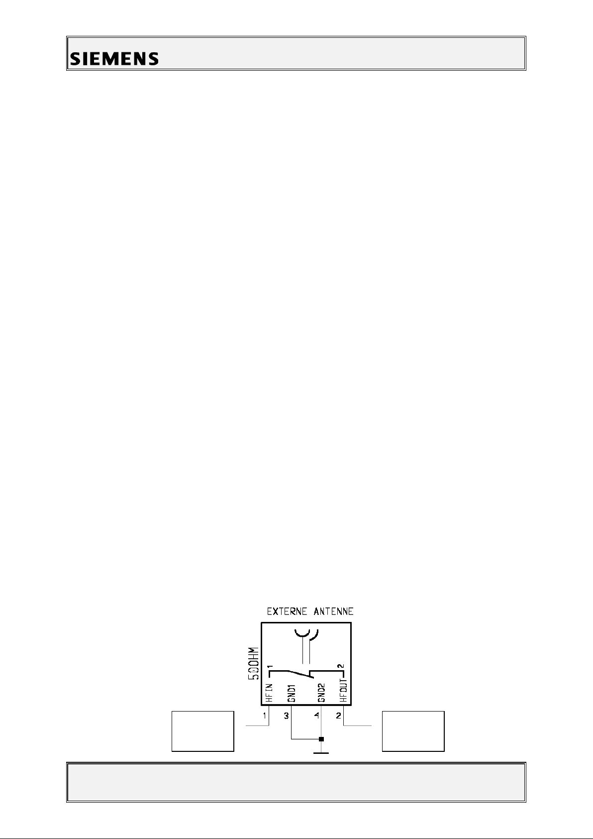
2.2.3 Component Information
The Antenna Connector is a mechanical switch operated by the RF plug of a carkit or, for testing
purposes, of an RF clip.
Normally the RF signal goes to and comes from the internal antenna. Whenever an RF plug is plugged
into the antenna connector the connection to the internal antenna is opened and the connection to the
external antenna socket is made. See drawing below.
V1.3 Page 4 of 41 ICM D CC ST
D. Schnoor
12/01
Page 5

Information and Communication Mobile
Devices
2.3 Priority:
........ Mandatory
........ Repair
........ Optional
........ Not Yet Defined
2.4 Repair Documentation
2.4.1 Description of procedure:
2.4.1.1 Diagnosis
Check the output power of the handset with the LSO testprogram.
Especially watch the external antenna power!
2.4.1.2 Repair by component change
Use hot air blower to remove defective connector
Avoid excessive heat!
Watch surrounding components!
Resolder new connector afterwards.
2.4.1.3 Repair by SW-Booting
Not possible!
2.4.1.4 Test
Retest handset after repair as described above.
2.4.2 List of needed material
2.4.2.1 Components
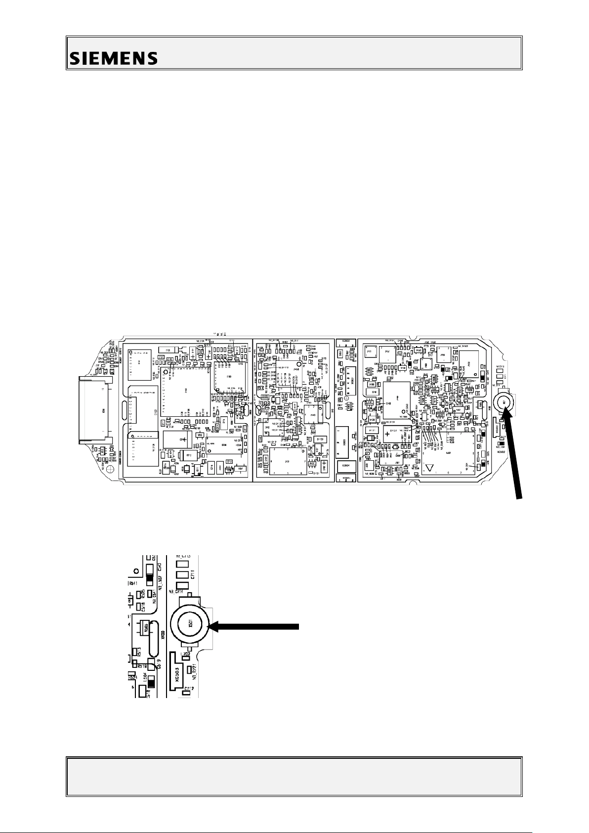
X35 antenna connector
Attention: This is not the same connector as C25/S25 !!!
Part-Number: L36334-Z93-C272
V1.3 Page 5 of 41 ICM D CC ST
D. Schnoor
12/01
Page 6
Information and Communication Mobile
Figure 1: X35 Board Antenna Connector Side (Top View)
Figure 2: X35 Antenna Connector Placement (X501) (Top View)
Devices
2.4.2.2 Jigs and Tools
Hot Air Blower
Soldering Iron
2.4.2.3 Special Tools
None
2.4.2.4 Working materials
Desolder Wick / Braid
Solder
2.4.3 Drawings
V1.3 Page 6 of 41 ICM D CC ST
D. Schnoor
12/01
Page 7

Information and Communication Mobile
Devices
3 Ringer
3.1 Affected Units
3.1.1 Type: C/M/S35
3.1.2 Affected IMEIs / Date Codes: All / All
3.1.3 Affected SW-Versions: All
3.2 Fault Description
3.2.1 Fault Symptoms for customers:
Problems with the handset ringer. No ringer tone
audible.
3.2.2 Fault Symptom on GSM-Tester:
Handset fails ringer test.
3.3 Priority:
........ Mandatory
........ Repair
........ Optional
........ Not Yet Defined
V1.3 Page 7 of 41 ICM D CC ST
D. Schnoor
12/01
Page 8

Information and Communication Mobile
Devices
3.4 Repair Documentation
3.4.1 Description of procedure:
3.4.1.1 Diagnosis
Visually check the ringer. Watch for physical damage or dry joints.
3.4.1.2 Repair by component change
Resolder dry soldering joints.
If the ringer is physically damaged use hot air blower or wick to remove
defective connector.
Avoid excessive heat!
Watch surrounding components!
Resolder new ringer afterwards.
3.4.1.3 Repair by SW-Booting
Not possible!
3.4.1.4 Test
Retest handset after repair.
3.4.2 List of needed material
3.4.2.1 Components
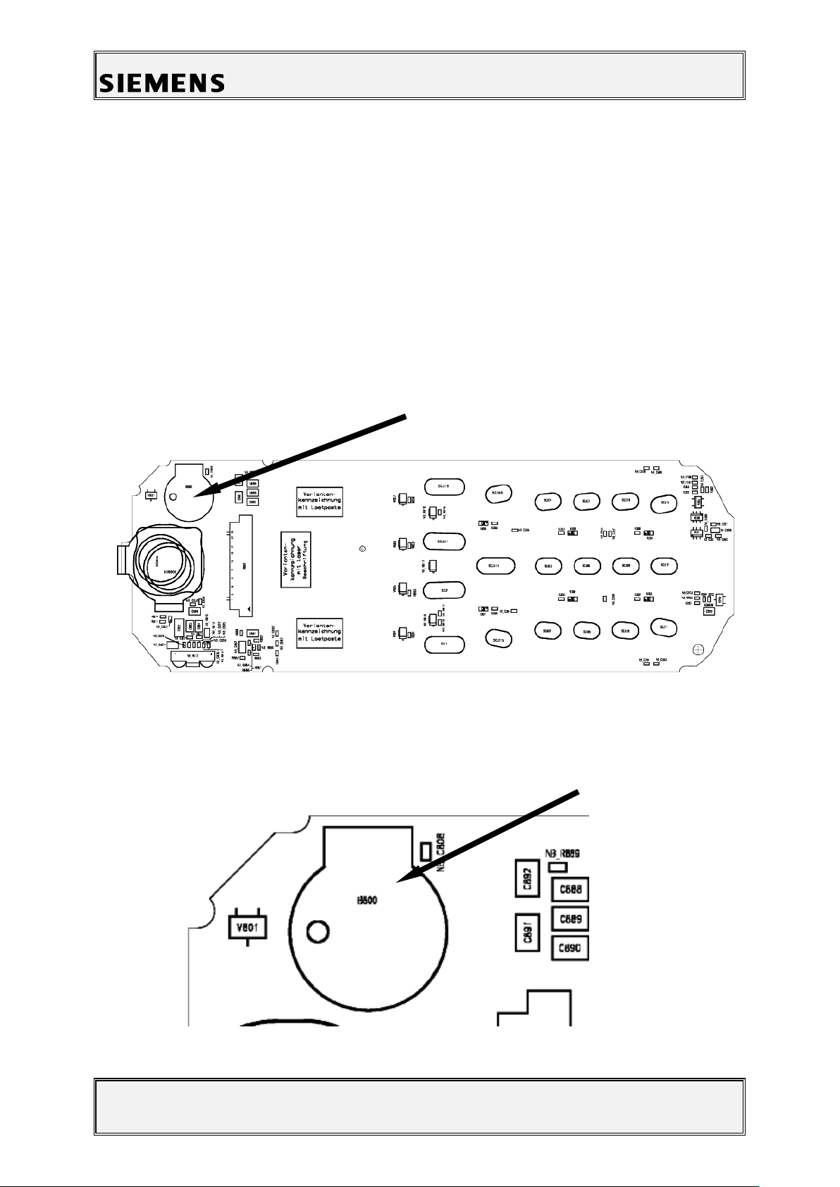
Ringer P35:
Part-Number: L36178-Z2-C26
3.4.2.2 Jigs and Tools
Hot Air Blower
Soldering Iron
V1.3 Page 8 of 41 ICM D CC ST
D. Schnoor
12/01
Page 9
Information and Communication Mobile
Figure 1: X35 Board Ringer Side
Figure 2: X35 Ringer (B800) Placement (Top View)
Devices
3.4.2.3 Special Tools
None
3.4.2.4 Working materials
Desolder Wick / Braid
Solder
Flux
3.4.3 Drawings
V1.3 Page 9 of 41 ICM D CC ST
D. Schnoor
12/01
Page 10
Information and Communication Mobile
Devices
4 Bottom Connector (Lumberg)
4.1 Affected Units
4.1.1 Type: C/M/S35
4.1.2 Affected IMEIs / Date Codes: All / All
4.1.3 Affected SW-Versions: All
4.2 Fault Description
4.2.1 Fault Symptoms for customers:
Charging problems.
Problems with external loudspeaker or microphone
when using a car kit.
Problems with accessories connected at the bottom
connector.
Problems with SW booting.
4.2.2 Fault Symptom on GSM-Tester:
This problem cannot be detected with a GSM-Tester.
4.3 Priority:
........ Mandatory
........ Repair
........ Optional
........ Not Yet Defined
V1.3 Page 10 of 41 ICM D CC ST
D. Schnoor
12/01
Page 11

Information and Communication Mobile
Devices
4.4 Repair Documentation
4.4.1 Description of procedure:
4.4.1.1 Diagnosis
Visually check the bottom connector. Watch for dry joints!
4.4.1.2 Repair by component change
Use hot air blower remove defective bottom connector.
Avoid excessive heat!
Watch surrounding components!
Resolder new bottom connector afterwards.
4.4.1.3 Repair by SW-Booting
Not possible!
4.4.1.4 Test
Retest handset after repair.
4.4.2 List of needed material
4.4.2.1 Components
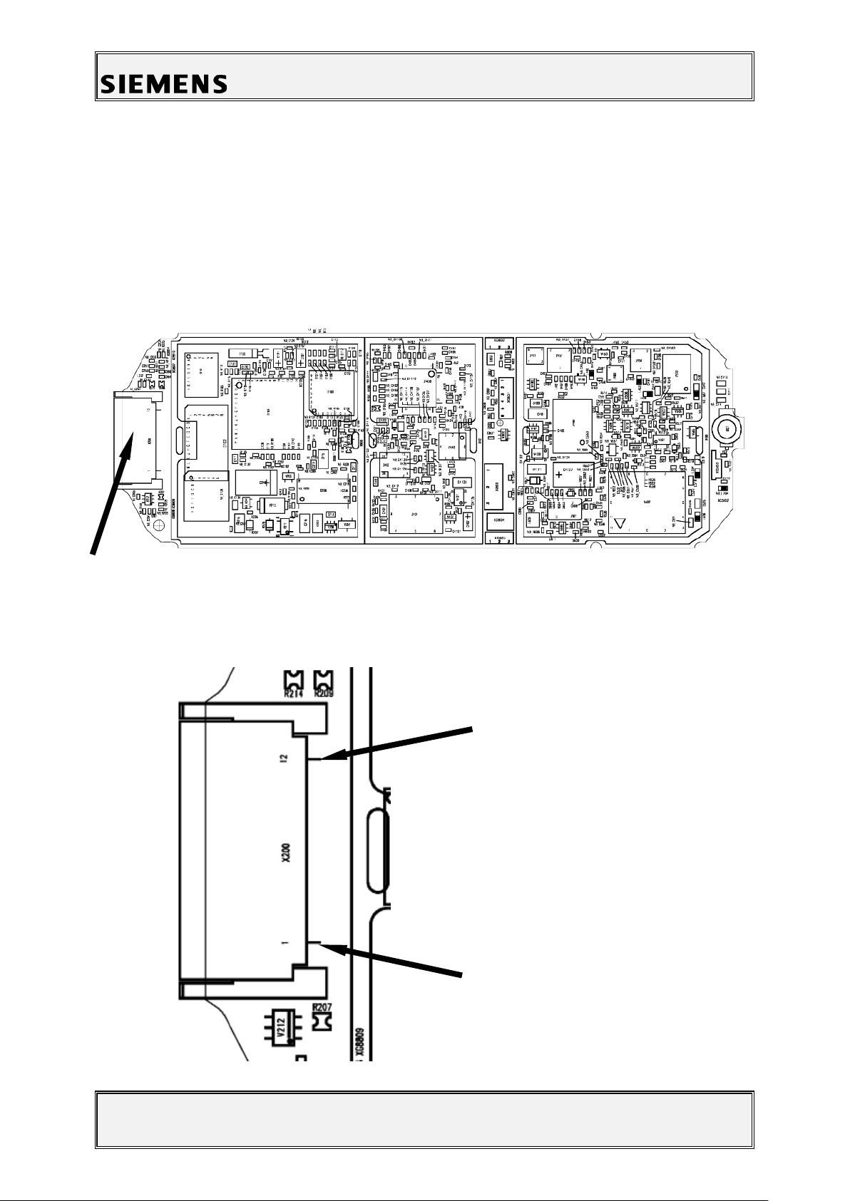
Bottom Connector X35
Part-Number: L36334-Z93-C262
4.4.2.2 Jigs and Tools
Hot Air Blower
Soldering Iron
4.4.2.3 Special Tools
None
V1.3 Page 11 of 41 ICM D CC ST
D. Schnoor
12/01
Page 12
Information and Communication Mobile
Figure 1: X35 Board Bottom Connector Side
Figure 2: X35 Bottom Connector Placement (Top View)
Pin 12
Pin 1
Devices
4.4.2.4 Working materials
Desolder Wick / Braid
Solder
4.4.3 Drawings
V1.3 Page 12 of 41 ICM D CC ST
D. Schnoor
12/01
Page 13

Information and Communication Mobile
Pin
Name
IN/OUT
Notes
1
GND
2
SB
I/O
Charger coding and
charger control.
3
POWER
I
Charging Current
4
FBatt+
O
Power supply for the
accessories.
5
TX O Serial interface
6
RX I Serial interface
7
ZUB_CLK
I/O
Clock line for
accessory bus
Use as DTC In data
operation
8
ZUB_DATA
I/O
Data line for
accessory bus.
Use as CTS in data
operation
9
GND_MIC
For external
microphone
10
HF_MIC
I
External microphone
11
AUDO
O
Trigger for external
loudspeaker
12
GNDA
For external
loudspeaker
Table 1: X35 Bottom Connector Pin Description
Devices
V1.3 Page 13 of 41 ICM D CC ST
D. Schnoor
12/01
Page 14

Information and Communication Mobile
Devices
5 Display Connector
5.1 Affected Units
5.1.1 Type: C/M/S 35
5.1.2 Affected IMEIs / Date Codes: All / All
5.1.3 Affected SW-Versions: All
5.2 Fault Description
5.2.1 Fault Symptoms for customers:
Display problems, like missing lines or columns on the
LCD or display contrast problems.
5.2.2 Fault Symptom on GSM-Tester:
Display test fails.
5.3 Priority:
........ Mandatory
........ Repair
........ Optional
........ Not Yet Defined
V1.3 Page 14 of 41 ICM D CC ST
D. Schnoor
12/01
Page 15

Information and Communication Mobile
Devices
5.4 Repair Documentation
5.4.1 Description of procedure:
5.4.1.1 Diagnosis
Visually check the status of the display connector. Watch for oxidation
and dry solder joints.
Mechanically check the opening / closing mechanism.
5.4.1.2 Repair by component change
Use hot air to remove defective connector
Avoid excessive heat!
Watch surrounding components!!
Resolder new connector afterwards
5.4.1.3 Repair by SW-Booting
Not possible!
5.4.1.4 Test
Retest handset after repair.
V1.3 Page 15 of 41 ICM D CC ST
D. Schnoor
12/01
Page 16

Information and Communication Mobile
Devices
5.4.2 List of needed material
5.4.2.1 Components Display connector
Part-Number: L36195-Z26-C629
5.4.2.2 Jigs and Tools
Soldering Iron
Hot Air Blower
5.4.2.3 Special Tools
None
5.4.2.4 Working materials
Desolder Wick / Braid
Solder
V1.3 Page 16 of 41 ICM D CC ST
D. Schnoor
12/01
Page 17

Information and Communication Mobile
Figure 1: X35 board display connector side
Figure 2: X35 display connector placement (Top View)
Devices
5.4.3 Drawings
V1.3 Page 17 of 41 ICM D CC ST
D. Schnoor
12/01
Page 18

Information and Communication Mobile
Devices
6 Keyboard LEDs
6.1 Affected Units
6.1.1 Type: C/M/S 35
6.1.2 Affected IMEIs / Date Codes: All / All
6.1.3 Affected SW-Versions: All
6.2 Fault Description
6.2.1 Fault Symptoms for customers:
Keyboard Illumination not working.
6.2.2 Fault Symptom on GSM-Tester:
This fault cannot be detected with a GSM-Tester
6.3 Priority:
........ Mandatory
........ Repair
........ Optional
........ Not Yet Defined
V1.3 Page 18 of 41 ICM D CC ST
D. Schnoor
12/01
Page 19

Information and Communication Mobile
Devices
6.4 Repair Documentation
6.4.1 Description of procedure:
6.4.1.1 Diagnosis
Use the diode test function of a multimeter to check the status of the
diode.
The typical voltage drop on the diode is 1.7V when testing the diode
function with the multimeter.
6.4.1.2 Repair by component change
Use soldering iron to remove defective diode
Avoid excessive heat!
Watch surrounding components!
Resolder new diode afterwards.
6.4.1.3 Repair by SW-Booting
Not possible!
6.4.1.4 Test
Retest handset after repair.
6.4.2 List of needed material
6.4.2.1 Components
LED keyboard X35
Part-Number: L36840-L2031-D670
6.4.2.2 Jigs and Tools
Hot Air Blower
Soldering Iron
V1.3 Page 19 of 41 ICM D CC ST
D. Schnoor
12/01
Page 20

Information and Communication Mobile
Figure 1: X35 board keyboard LED Side
Figure 2: X35 keyboard LED placement and polarity (top view)
Devices
6.4.2.3 Special Tools
None
6.4.2.4 Working materials
Desolder Wick / Braid
Solder
6.4.3 Drawings
V1.3 Page 20 of 41 ICM D CC ST
D. Schnoor
12/01
Page 21

Information and Communication Mobile
Devices
7 Display LEDs
7.1 Affected Units
7.1.1 Type: C/M/S 35
7.1.2 Affected IMEIs / Date Codes: All / All
7.1.3 Affected SW-Versions: All
7.2 Fault Description
7.2.1 Fault Symptoms for customers:
Display Illumination not working.
7.2.2 Fault Symptom on GSM-Tester:
This fault cannot be detected with a GSM-Tester
7.3 Priority:
........ Mandatory
........ Repair
........ Optional
........ Not Yet Defined
V1.3 Page 21 of 41 ICM D CC ST
D. Schnoor
12/01
Page 22

Information and Communication Mobile
Devices
7.4 Repair Documentation
7.4.1 Description of procedure:
7.4.1.1 Diagnosis
Use the diode test function of a multimeter to check the status of the
diode.
The typical voltage drop on the diode is 1.7V when testing the diode
function with the multimeter.
Attention: There are two different types of display LEDs, one for
C/M35 and one for S35! Also they use different placement
location, see drawings 1 and 3.
7.4.1.2 Repair by component change
Use soldering iron to remove defective diode
Avoid excessive heat!
Watch surrounding components!
Resolder new diode afterwards.
7.4.1.3 Repair by SW-Booting
Not possible!
7.4.1.4 Test
Retest handset after repair.
7.4.2 List of needed material
7.4.2.1 Components
Display LED S35
Part-Number: L36840-L2048-D670
Display LED C/M35
Part-Number: L36840-L2047-D670
7.4.2.2 Jigs and Tools
Hot Air Blower
Soldering Iron
V1.3 Page 22 of 41 ICM D CC ST
D. Schnoor
12/01
Page 23

Information and Communication Mobile
Figure 1: C/M35 board display LED Side
Figure 2: C/M35 board display LED placement and polarity
Devices
7.4.2.3 Special Tools
None
7.4.2.4 Working materials
Desolder Wick / Braid
Solder
7.4.3 Drawings
V1.3 Page 23 of 41 ICM D CC ST
D. Schnoor
12/01
Page 24

Information and Communication Mobile
Figure 3: S35 board display LED side
Figure 4: S35 board display LED placement and polarity
Devices
V1.3 Page 24 of 41 ICM D CC ST
D. Schnoor
12/01
Page 25

Information and Communication Mobile
Devices
8 Infrared Diodes
8.1 Affected Units
8.1.1 Type: S 35
8.1.2 Affected IMEIs / Date Codes: All / All
8.1.3 Affected SW-Versions: All
8.2 Fault Description
8.2.1 Fault Symptoms for customers:
No infrared connection possible.
8.2.2 Fault Symptom on GSM-Tester:
This fault cannot be detected with a GSM-Tester.
8.3 Priority:
........ Mandatory
........ Repair
........ Optional
........ Not Yet Defined
V1.3 Page 25 of 41 ICM D CC ST
D. Schnoor
12/01
Page 26

Information and Communication Mobile
Devices
8.4 Repair Documentation
8.4.1 Description of procedure:
8.4.1.1 Diagnosis
Visually check the status of the IrDa module. Watch for dry solder
joints.
Use a reference infrared port (eg. from a notebook) to check the IrDa
function. If the notebook recognizes the S35, the infrared function is
ok.
8.4.1.2 Repair by component change
Use hot air to remove defective infrared module.
Avoid excessive heat!
Watch surrounding components!!
Resolder new module afterwards
8.4.1.3 Repair by SW-Booting
Not possible!
8.4.1.4 Test
Retest handset after repair.
V1.3 Page 26 of 41 ICM D CC ST
D. Schnoor
12/01
Page 27

Information and Communication Mobile
Devices
8.4.2 List of needed material
8.4.2.1 Components Infrared module S35
Part-Number: L36810-U6030-D670
8.4.2.2 Jigs and Tools
Soldering Iron
Hot Air Blower
8.4.2.3 Special Tools
None
8.4.2.4 Working materials
Desolder Wick / Braid
Solder
V1.3 Page 27 of 41 ICM D CC ST
D. Schnoor
12/01
Page 28

Information and Communication Mobile
Figure 1: S35 board infrared module side
Figure 2: S35 infrared module placement (Top View)
Devices
8.4.3 Drawings
V1.3 Page 28 of 41 ICM D CC ST
D. Schnoor
12/01
Page 29

Information and Communication Mobile
Devices
9 Charging Diode V210
9.1 Affected Units
9.1.1 Type: C/M/S35
9.1.2 Affected IMEIs / Date Codes: All / All
9.1.3 Affected SW-Versions: All
9.2 Fault Description
9.2.1 Fault Symptoms for customers:
Charging symbol in the display even if no charger is
connected.
Very low standby time and deeply discharged batteries.
9.2.2 Fault Symptom on GSM-Tester:
This fault cannot be detected with a GSM-Tester.
9.3 Priority:
........ Mandatory
........ Repair
........ Optional
........ Not Yet Defined
V1.3 Page 29 of 41 ICM D CC ST
D. Schnoor
12/01
Page 30

Information and Communication Mobile
Charging
Voltage
input
V210
a)
b)
Devices
9.4 Repair Documentation
9.4.1 Description of procedure:
9.4.1.1 General Information
The purpose of the diode V210 is to prevent the feedback of the
battery voltage to the charging circuitry. That would make the
microprocessor detect a charging voltage which is not present in reality
causing
a) The charging symbol to appear on the display and/or
b) The battery to be drained constantly, even when the phone is
switched off.
The above circuit diagram extract shows the power supply IC including the charging circuitry.
The charging voltage coming from the bottom connector is called POWER and it is
connected to the charging circuitry a) and to the microporocessor as a signal called
EXT_POWER_UC. This signal is the charging voltage divided down by the two resistors
R227 and R229 and it is led to one of the microprocessor port pins. It indicates the presence
of the charger to the microprocessor triggering the display of the charging symbol.
V1.3 Page 30 of 41 ICM D CC ST
D. Schnoor
12/01
Page 31

Information and Communication Mobile
Devices
If the diode V210 is defective it opens from pin one to pin 2, meaning it does not block the
battery voltage from going to the charging transistor V211 anymore. This FET has a
(unwanted) diode from pin 2,5,6 to pin 4 which opens and connects the battery voltage with
the POWER signal and therefore also with the EXT_POWER_UC signal. In this case the
charging symbol appears on the display. Sometimes, if the battery voltage is very low, the
charging symbol may not appear, but the constant current flow will discharge the battery
anyway, even when the phone is switched off.
This will of course significantly reduce the standby time and may even lead to a
deeply discharged battery!
9.4.1.2 Diagnosis
Check the status (reverse blocking) of the diode V210 with a
multimeter.
9.4.1.3 Repair by component change
Use soldering iron to remove defective diode.
Avoid excessive heat!
Watch surrounding components!!
Resolder new diode afterwards
9.4.1.4 Repair by SW-Booting
Not possible!
V1.3 Page 31 of 41 ICM D CC ST
D. Schnoor
12/01
Page 32

Information and Communication Mobile
Devices
9.4.1.5 Test
Retest handset after repair
9.4.2 List of needed material
9.4.2.1 Components Diode V210
Part-Number: L36840-D5055-D670
9.4.2.2 Jigs and Tools
Soldering Iron
Hot Air Blower
9.4.2.3 Special Tools
None
9.4.2.4 Working materials
Desolder Wick / Braid
Solder
V1.3 Page 32 of 41 ICM D CC ST
D. Schnoor
12/01
Page 33

Information and Communication Mobile
Figure 1: X35 V210 side
Figure 2: X35 V210 placement (Top View)
Devices
9.4.3 Drawings
V1.3 Page 33 of 41 ICM D CC ST
D. Schnoor
12/01
Page 34

Information and Communication Mobile
Devices
10 Diplexer Z503
10.1 Affected Units
10.1.1 Type: C/M/S35
10.1.2 Affected IMEIs / Date Codes: All / All
10.1.3 Affected SW-Versions: All
10.2 Fault Description
10.2.1 Fault Symptoms for customers:
Handset cannot register with the GSM-900 network.
10.2.2 Fault Symptom on GSM-Tester:
Handset Rx-Sensitivity is too low.
10.3 Priority:
........ Mandatory
........ Repair
........ Optional
........ Not Yet Defined
V1.3 Page 34 of 41 ICM D CC ST
D. Schnoor
12/01
Page 35

Information and Communication Mobile
a)
Z503
Devices
10.4 Repair Documentation
10.4.1 Description of procedure:
10.4.1.1 General Information
The purpose of the diplexer is the following:
A) Switching the Rx RF signal coming from the antenna to either the
GSM-900 or GSM-1800 receiver chain.
B) Switching of the Tx RF signal from either the GSM-900 or GSM-
1800 Tx output to the antenna.
V1.3 Page 35 of 41 ICM D CC ST
D. Schnoor
12/01
Page 36

Information and Communication Mobile
Devices
The above circuit diagram extract shows the diplexer IC including the external circuitry. The
diplexer switching direction is controlled by the four control inputs VC1 (pin 2), VC2 (4), VC3
(8), VC4 (10).
The input VC2 is used to switch the Rx_GSM-900 direction. If the diplexer is defective then
the diplexer cannot switch to this direction anymore. As a result of this the phone loses about
25-30 dB when receiving GSM-900 signals.
Important: There are two different types of diplexer used for C/M/S35. Only the silver
type produced by Murata, labeled with a small M is affected by the problem
described above.
There is also another type produced by TDK. This type has a golden housing
and a small hole in the upper right corner. This type is not affected. The
different types have a different external circuitry and are not interchangeable!
10.4.1.2 Diagnosis
Check the status of the diplexer Z503 with a multimeter. Measure the
resistance of pin 4 against ground. It must be around 20k Ohms. If the
diplexer is defective the measured value will be significantly lower, e.g.
2k Ohms. This value however may differ.
Note:
To make the measurement easier, as seen in the circuit diagram
above, you can also use pin 6 of V506. This pin can be reached easier
than pin 4 of Z503.
10.4.1.3 Repair by component change
Use hot air to remove defective diplexer.
Avoid excessive heat!
Watch surrounding components!!
Resolder new diplexer afterwards.
10.4.1.4 Repair by SW-Booting
Not possible!
10.4.1.5 Test
Retest handset after repair
V1.3 Page 36 of 41 ICM D CC ST
D. Schnoor
12/01
Page 37

Information and Communication Mobile
Devices
10.4.2 List of needed material
10.4.2.1 Components
Diplexer Z503
Part-Number: L36145-K280-Y137
10.4.2.2 Jigs and Tools
Soldering Iron
Hot Air Blower
10.4.2.3 Special Tools
None
10.4.2.4 Working materials
Desolder Wick / Braid
Solder
V1.3 Page 37 of 41 ICM D CC ST
D. Schnoor
12/01
Page 38

Information and Communication Mobile
Figure 1: X35 Z503 side
Figure 2: X35 Z503 placement (Top View)
Pin 6 of V506
Devices
10.4.3 Drawings
V1.3 Page 38 of 41 ICM D CC ST
D. Schnoor
12/01
Page 39

Information and Communication Mobile
Devices
11 Voltage Protection Diode V279
11.1 Affected Units
11.1.1 Type: C/M/S35
11.1.2 Affected IMEIs / Date Codes: All / All
11.1.3 Affected SW-Versions: All
11.2 Fault Description
11.2.1 Fault Symptoms for customers:
External equipment which needs power via the I/O
connector does not work.
11.2.2 Fault Symptom on GSM-Tester:
BATT+ rises too fast
11.3 Priority:
........ Mandatory
........ Repair
........ Optional
........ Not Yet Defined
V1.3 Page 39 of 41 ICM D CC ST
D. Schnoor
12/01
Page 40

Information and Communication Mobile
Devices
11.4 Repair Documentation
11.4.1 Description of procedure:
11.4.1.1 General Information
The purpose of the diode V279 is to prevent the feedback of external
connected equipment. An external voltage, connected to the I/O
connector, may damage the accumulator.
11.4.1.2 Diagnosis
Check the status (reverse blocking) of the diode V279 with a
multimeter.
11.4.1.3 Repair by component change
Use soldering iron to remove defective diode.
Avoid excessive heat!
Watch surrounding components!!
Resolder new diode afterwards
11.4.1.4 Repair by SW-Booting
Not possible!
11.4.1.5 Test
Retest handset after repair
11.4.2 List of needed material
11.4.2.1 Components
Diode V279
Part-Number: L36840-D5059-D670
11.4.2.2 Jigs and Tools
Soldering Iron
Hot Air Blower
V1.3 Page 40 of 41 ICM D CC ST
D. Schnoor
12/01
Page 41

Information and Communication Mobile
V279
Devices
11.4.2.3 Special Tools
None
11.4.2.4 Working materials
Desolder Wick / Braid
Solder
11.4.2.5 Drawings
Figure 1: X35 V279 side
Figure 2: X35 V279 placement (Top View)
V1.3 Page 41 of 41 ICM D CC ST
D. Schnoor
12/01
 Loading...