


C167Derivatives
16-Bit CMOS Single-Chip Microcontrollers
User's Manual 03.96 Version 2.0
http://www.siemens.de/
Semiconductor/

C167
Revision History: Version 2.0 (03.96)
Previous Version: Version 1.0 (08.94)
Preliminary User’s Manual Revision 1.0 (07.92)
Page
(in previous
Version)
Page
Subjects (major changes since last revision)
(in current
Version)
– Extension of document scope to C167CR, C167SR, C167S
– Correction of the items published in the paper "Corrections C167"
Edition 03.96
This edition was realized using the software system FrameMaker
Published by Siemens AG,
Bereich Halbleiter, Marketing-
Kommunikation, Balanstraße 73,
81541 München
©
Siemens AG 1996.
All Rights Reserved.
Attention please!
As far as patents or other rights of third parties are conc erned, liability is only assumed for components, not for app lic ations, processes
and circuits implemented within components or assemblies.
The information describes the type of component and shall not be conside red as as sured characteristics.
Terms of delivery and rights to change design res erved.
For questions on technology, delivery and prices please contact the Semiconductor Group Offices in Germany or the Siemens Companies
and Representatives worldwide (see address list).
Due to technical requirements components m ay contain dangerous substances. For information on the types in question please contact
your nearest Siemens Office, Sem iconductor Group.
Siemens AG is an approved CECC manufacturer.
Packing
Please use the recycling operators know n to you. We can also help you – get in touch with your near est sales office. By agreement we
will take packing material back, if it is sorted. You must bear the costs of transport.
For packing material that is returned to us unsorted or which we are not obliged to accept, we shall have to invoice you for any costs incurred.
Components used in life-support devices or systems must be expressly authorized for such purpose!
Critical components
written approval of the Semiconductor Group of Siemens AG.
1 A critical component is a component used in a life-support device or system whose failure can reasonably be expected to cause the
failure of that life-support device or system, or to affect its safet y or ef fectiv eness of that device or system.
2 Life support devices or systems are intended (a) to be implante d in the human body, or (b) to su pport and/o r maintain a nd sustain hu-
man life. If they fail, it is reasonable to assume that the health of the user may be endangered.
1
of the Semiconductor Group of Siemens AG, may only be used in life-support devices or systems2 with the express
.

C167
Table of Contents Page
1 Introduction . . . . . . . . . . . . . . . . . . . . . . . . . . . . . . . . . . . . . . . . . . . . . . . . 1-1
1.1 The Members of the 16-bit Microcontroller Family . . . . . . . . . . . . . . . . . . . . 1-2
1.2 Summary of Basic Features . . . . . . . . . . . . . . . . . . . . . . . . . . . . . . . . . . . . . 1-4
1.3 Abbreviations . . . . . . . . . . . . . . . . . . . . . . . . . . . . . . . . . . . . . . . . . . . . . . . . 1-7
2 Architectural Overview . . . . . . . . . . . . . . . . . . . . . . . . . . . . . . . . . . . . . . . 2-1
2.1 Basic CPU Concepts and Optimizations . . . . . . . . . . . . . . . . . . . . . . . . . . . 2-2
2.1.1 High Instruction Bandwidth / Fast Execution . . . . . . . . . . . . . . . . . . . . . . . . 2-3
2.1.2 Programmable Multiple Priority Interrupt System . . . . . . . . . . . . . . . . . . . . . 2-6
2.2 The On-chip System Resources . . . . . . . . . . . . . . . . . . . . . . . . . . . . . . . . . 2-7
2.3 The On-chip Peripheral Blocks . . . . . . . . . . . . . . . . . . . . . . . . . . . . . . . . . 2-11
2.4 Protected Bits . . . . . . . . . . . . . . . . . . . . . . . . . . . . . . . . . . . . . . . . . . . . . . . 2-17
3 Memory Organization . . . . . . . . . . . . . . . . . . . . . . . . . . . . . . . . . . . . . . . . 3-1
3.1 Internal ROM . . . . . . . . . . . . . . . . . . . . . . . . . . . . . . . . . . . . . . . . . . . . . . . . 3-3
3.2 Internal RAM and SFR Area . . . . . . . . . . . . . . . . . . . . . . . . . . . . . . . . . . . . 3-4
3.3 The On-Chip XRAM . . . . . . . . . . . . . . . . . . . . . . . . . . . . . . . . . . . . . . . . . . . 3-9
3.4 External Memory Space . . . . . . . . . . . . . . . . . . . . . . . . . . . . . . . . . . . . . . . 3-11
3.5 Crossing Memory Boundaries . . . . . . . . . . . . . . . . . . . . . . . . . . . . . . . . . . 3-12
4 The Central Processing Unit (CPU) . . . . . . . . . . . . . . . . . . . . . . . . . . . . . 4-1
4.1 Instruction Pipelining . . . . . . . . . . . . . . . . . . . . . . . . . . . . . . . . . . . . . . . . . . 4-3
4.1.1 Particular Pipeline Effects . . . . . . . . . . . . . . . . . . . . . . . . . . . . . . . . . . . . . . 4-6
4.2 Bit-Handling and Bit-Protection . . . . . . . . . . . . . . . . . . . . . . . . . . . . . . . . . . 4-9
4.3 Instruction State Times . . . . . . . . . . . . . . . . . . . . . . . . . . . . . . . . . . . . . . . 4-10
4.4 CPU Special Function Registers . . . . . . . . . . . . . . . . . . . . . . . . . . . . . . . . 4-11
5 Interrupt and Trap Functions . . . . . . . . . . . . . . . . . . . . . . . . . . . . . . . . . . 5-1
5.1 Interrupt System Structure . . . . . . . . . . . . . . . . . . . . . . . . . . . . . . . . . . . . . . 5-2
5.1.1 Interrupt Control Registers . . . . . . . . . . . . . . . . . . . . . . . . . . . . . . . . . . . . . . 5-6
5.2 Operation of the PEC Channels . . . . . . . . . . . . . . . . . . . . . . . . . . . . . . . . . 5-11
5.3 Prioritization of Interrupt and PEC Service Requests . . . . . . . . . . . . . . . . 5-14
5.4 Saving the Status during Interrupt Service . . . . . . . . . . . . . . . . . . . . . . . . . 5-15
5.5 Interrupt Response Times . . . . . . . . . . . . . . . . . . . . . . . . . . . . . . . . . . . . . 5-17
5.5.1 PEC Response Times . . . . . . . . . . . . . . . . . . . . . . . . . . . . . . . . . . . . . . . . 5-19
5.6 External Interrupts . . . . . . . . . . . . . . . . . . . . . . . . . . . . . . . . . . . . . . . . . . . 5-21
5.7 Trap Functions . . . . . . . . . . . . . . . . . . . . . . . . . . . . . . . . . . . . . . . . . . . . . . 5-24
6 Parallel Ports . . . . . . . . . . . . . . . . . . . . . . . . . . . . . . . . . . . . . . . . . . . . . . . 6-1
6.1 PORT0 . . . . . . . . . . . . . . . . . . . . . . . . . . . . . . . . . . . . . . . . . . . . . . . . . . . . . 6-5
6.1.1 Alternate Functions of PORT0 . . . . . . . . . . . . . . . . . . . . . . . . . . . . . . . . . . . 6-6
6.2 PORT1 . . . . . . . . . . . . . . . . . . . . . . . . . . . . . . . . . . . . . . . . . . . . . . . . . . . . . 6-8
6.2.1 Alternate Functions of PORT1 . . . . . . . . . . . . . . . . . . . . . . . . . . . . . . . . . . . 6-9
6.3 Port 2 . . . . . . . . . . . . . . . . . . . . . . . . . . . . . . . . . . . . . . . . . . . . . . . . . . . . . 6-11
6.3.1 Alternate Functions of Port 2 . . . . . . . . . . . . . . . . . . . . . . . . . . . . . . . . . . . 6-12
Semiconductor Group I-1

C167
Table of Contents Page
6.4 Port 3 . . . . . . . . . . . . . . . . . . . . . . . . . . . . . . . . . . . . . . . . . . . . . . . . . . . . . 6-15
6.4.1 Alternate Functions of Port 3 . . . . . . . . . . . . . . . . . . . . . . . . . . . . . . . . . . . 6-16
6.5 Port 4 . . . . . . . . . . . . . . . . . . . . . . . . . . . . . . . . . . . . . . . . . . . . . . . . . . . . . 6-20
6.5.1 Alternate Functions of Port 4 . . . . . . . . . . . . . . . . . . . . . . . . . . . . . . . . . . . 6-20
6.6 Port 5 . . . . . . . . . . . . . . . . . . . . . . . . . . . . . . . . . . . . . . . . . . . . . . . . . . . . . 6-23
6.6.1 Alternate Functions of Port 5 . . . . . . . . . . . . . . . . . . . . . . . . . . . . . . . . . . . 6-23
6.7 Port 6 . . . . . . . . . . . . . . . . . . . . . . . . . . . . . . . . . . . . . . . . . . . . . . . . . . . . . 6-25
6.7.1 Alternate Functions of Port 6 . . . . . . . . . . . . . . . . . . . . . . . . . . . . . . . . . . . 6-26
6.8 Port 7 . . . . . . . . . . . . . . . . . . . . . . . . . . . . . . . . . . . . . . . . . . . . . . . . . . . . . 6-30
6.8.1 Alternate Functions of Port 7 . . . . . . . . . . . . . . . . . . . . . . . . . . . . . . . . . . . 6-31
6.9 Port 8 . . . . . . . . . . . . . . . . . . . . . . . . . . . . . . . . . . . . . . . . . . . . . . . . . . . . . 6-34
6.9.1 Alternate Functions of Port 8 . . . . . . . . . . . . . . . . . . . . . . . . . . . . . . . . . . . 6-35
7 Dedicated Pins . . . . . . . . . . . . . . . . . . . . . . . . . . . . . . . . . . . . . . . . . . . . . . 7-1
8 The External Bus Interface . . . . . . . . . . . . . . . . . . . . . . . . . . . . . . . . . . . . 8-1
8.1 External Bus Modes . . . . . . . . . . . . . . . . . . . . . . . . . . . . . . . . . . . . . . . . . . . 8-2
8.2 Programmable Bus Characteristics . . . . . . . . . . . . . . . . . . . . . . . . . . . . . . 8-10
8.3 READY Controlled Bus Cycles . . . . . . . . . . . . . . . . . . . . . . . . . . . . . . . . . 8-15
8.4 Controlling the External Bus Controller . . . . . . . . . . . . . . . . . . . . . . . . . . . 8-16
8.5 EBC Idle State . . . . . . . . . . . . . . . . . . . . . . . . . . . . . . . . . . . . . . . . . . . . . . 8-24
8.6 External Bus Arbitration . . . . . . . . . . . . . . . . . . . . . . . . . . . . . . . . . . . . . . . 8-25
8.7 The XBUS Interface . . . . . . . . . . . . . . . . . . . . . . . . . . . . . . . . . . . . . . . . . . 8-29
9 The General Purpose Timer Units . . . . . . . . . . . . . . . . . . . . . . . . . . . . . . 9-1
9.1 Timer Block GPT1 . . . . . . . . . . . . . . . . . . . . . . . . . . . . . . . . . . . . . . . . . . . . 9-1
9.1.1 GPT1 Core Timer T3 . . . . . . . . . . . . . . . . . . . . . . . . . . . . . . . . . . . . . . . . . . 9-3
9.1.2 GPT1 Auxiliary Timers T2 and T4 . . . . . . . . . . . . . . . . . . . . . . . . . . . . . . . . 9-8
9.1.3 Interrupt Control for GPT1 Timers . . . . . . . . . . . . . . . . . . . . . . . . . . . . . . . 9-15
9.2 Timer Block GPT2 . . . . . . . . . . . . . . . . . . . . . . . . . . . . . . . . . . . . . . . . . . . 9-16
9.2.1 GPT2 Core Timer T6 . . . . . . . . . . . . . . . . . . . . . . . . . . . . . . . . . . . . . . . . . 9-18
9.2.2 GPT2 Auxiliary Timer T5 . . . . . . . . . . . . . . . . . . . . . . . . . . . . . . . . . . . . . . 9-23
9.2.3 Interrupt Control for GPT2 Timers and CAPREL . . . . . . . . . . . . . . . . . . . . 9-31
10 The Asynchronous/Synchronous Serial Interface . . . . . . . . . . . . . . . . 10-1
10.1 Asynchronous Operation . . . . . . . . . . . . . . . . . . . . . . . . . . . . . . . . . . . . . . 10-4
10.2 Synchronous Operation . . . . . . . . . . . . . . . . . . . . . . . . . . . . . . . . . . . . . . . 10-8
10.3 Hardware Error Detection Capabilities . . . . . . . . . . . . . . . . . . . . . . . . . . . 10-10
10.4 ASC0 Baud Rate Generation . . . . . . . . . . . . . . . . . . . . . . . . . . . . . . . . . . 10-10
10.5 ASC0 Interrupt Control . . . . . . . . . . . . . . . . . . . . . . . . . . . . . . . . . . . . . . . 10-12
11 The High-Speed Synchronous Serial Interface . . . . . . . . . . . . . . . . . . . 11-1
11.1 Full-Duplex Operation . . . . . . . . . . . . . . . . . . . . . . . . . . . . . . . . . . . . . . . . 11-6
11.2 Half Duplex Operation . . . . . . . . . . . . . . . . . . . . . . . . . . . . . . . . . . . . . . . . 11-8
11.3 Baud Rate Generation . . . . . . . . . . . . . . . . . . . . . . . . . . . . . . . . . . . . . . . 11-10
Semiconductor Group I-2

C167
Table of Contents Page
11.4 Error Detection Mechanisms . . . . . . . . . . . . . . . . . . . . . . . . . . . . . . . . . . 11-12
11.5 SSC Interrupt Control . . . . . . . . . . . . . . . . . . . . . . . . . . . . . . . . . . . . . . . . 11-14
12 The Watchdog Timer (WDT) . . . . . . . . . . . . . . . . . . . . . . . . . . . . . . . . . . 12-1
12.0.1 Operation of the Watchdog Timer . . . . . . . . . . . . . . . . . . . . . . . . . . . . . . . 12-2
13 The Bootstrap Loader . . . . . . . . . . . . . . . . . . . . . . . . . . . . . . . . . . . . . . . 13-1
14 The Capture / Compare Units . . . . . . . . . . . . . . . . . . . . . . . . . . . . . . . . . 14-1
14.1 The CAPCOM Timers . . . . . . . . . . . . . . . . . . . . . . . . . . . . . . . . . . . . . . . . 14-4
14.2 CAPCOM Unit Timer Interrupts . . . . . . . . . . . . . . . . . . . . . . . . . . . . . . . . . 14-8
14.3 Capture/Compare Registers . . . . . . . . . . . . . . . . . . . . . . . . . . . . . . . . . . . 14-9
14.3.1 Selection of Capture Modes and Compare Modes . . . . . . . . . . . . . . . . . 14-11
14.4 Capture Mode . . . . . . . . . . . . . . . . . . . . . . . . . . . . . . . . . . . . . . . . . . . . . 14-12
14.5 Compare Modes, . . . . . . . . . . . . . . . . . . . . . . . . . . . . . . . . . . . . . . . . . . . 14-13
14.5.1 Double-Register Compare Mode . . . . . . . . . . . . . . . . . . . . . . . . . . . . . . . 14-18
14.6 Capture/Compare Interrupts . . . . . . . . . . . . . . . . . . . . . . . . . . . . . . . . . . 14-20
15 The Pulse Width Modulation Module . . . . . . . . . . . . . . . . . . . . . . . . . . . 15-1
15.1 Operating Modes . . . . . . . . . . . . . . . . . . . . . . . . . . . . . . . . . . . . . . . . . . . . 15-2
15.2 PWM Module Registers . . . . . . . . . . . . . . . . . . . . . . . . . . . . . . . . . . . . . . . 15-7
15.3 Interrupt Request Generation . . . . . . . . . . . . . . . . . . . . . . . . . . . . . . . . . . 15-11
15.4 PWM Output Signals . . . . . . . . . . . . . . . . . . . . . . . . . . . . . . . . . . . . . . . . 15-12
16 The Analog / Digital Converter . . . . . . . . . . . . . . . . . . . . . . . . . . . . . . . . 16-1
16.1 Mode Selection and Operation . . . . . . . . . . . . . . . . . . . . . . . . . . . . . . . . . . 16-3
16.2 Conversion Timing Control . . . . . . . . . . . . . . . . . . . . . . . . . . . . . . . . . . . . 16-10
16.3 A/D Converter Interrupt Control . . . . . . . . . . . . . . . . . . . . . . . . . . . . . . . . 16-11
17 System Reset . . . . . . . . . . . . . . . . . . . . . . . . . . . . . . . . . . . . . . . . . . . . . . 17-1
17.0.1 System Startup Configuration . . . . . . . . . . . . . . . . . . . . . . . . . . . . . . . . . . 17-7
18 Power Reduction Modes . . . . . . . . . . . . . . . . . . . . . . . . . . . . . . . . . . . . . 18-1
18.1 Idle Mode . . . . . . . . . . . . . . . . . . . . . . . . . . . . . . . . . . . . . . . . . . . . . . . . . . 18-1
18.2 Power Down Mode . . . . . . . . . . . . . . . . . . . . . . . . . . . . . . . . . . . . . . . . . . . 18-3
18.3 Status of Output Pins during Idle and Power Down Mode . . . . . . . . . . . . . 18-4
19 System Programming . . . . . . . . . . . . . . . . . . . . . . . . . . . . . . . . . . . . . . . 19-1
19.1 Stack Operations . . . . . . . . . . . . . . . . . . . . . . . . . . . . . . . . . . . . . . . . . . . . 19-4
19.2 Register Banking . . . . . . . . . . . . . . . . . . . . . . . . . . . . . . . . . . . . . . . . . . . . 19-8
19.3 Procedure Call Entry and Exit . . . . . . . . . . . . . . . . . . . . . . . . . . . . . . . . . . 19-8
19.4 Table Searching . . . . . . . . . . . . . . . . . . . . . . . . . . . . . . . . . . . . . . . . . . . . 19-11
19.5 Peripheral Control and Interface . . . . . . . . . . . . . . . . . . . . . . . . . . . . . . . 19-11
19.6 Floating Point Support . . . . . . . . . . . . . . . . . . . . . . . . . . . . . . . . . . . . . . . 19-12
19.7 Trap/Interrupt Entry and Exit . . . . . . . . . . . . . . . . . . . . . . . . . . . . . . . . . . 19-12
19.8 Unseparable Instruction Sequences . . . . . . . . . . . . . . . . . . . . . . . . . . . . 19-12
Semiconductor Group I-3

C167
Table of Contents Page
19.9 Overriding the DPP Addressing Mechanism . . . . . . . . . . . . . . . . . . . . . . 19-13
19.10 Handling the Internal ROM . . . . . . . . . . . . . . . . . . . . . . . . . . . . . . . . . . . . 19-14
19.11 Pits, Traps and Mines . . . . . . . . . . . . . . . . . . . . . . . . . . . . . . . . . . . . . . . 19-15
20 The Register Set . . . . . . . . . . . . . . . . . . . . . . . . . . . . . . . . . . . . . . . . . . . . 20-1
20.0.1 Register Description Format . . . . . . . . . . . . . . . . . . . . . . . . . . . . . . . . . . . 20-1
20.1 CPU General Purpose Registers (GPRs) . . . . . . . . . . . . . . . . . . . . . . . . . 20-2
20.2 Special Function Registers ordered by Name . . . . . . . . . . . . . . . . . . . . . . 20-4
20.3 Registers ordered by Address . . . . . . . . . . . . . . . . . . . . . . . . . . . . . . . . . 20-12
20.4 Special Notes . . . . . . . . . . . . . . . . . . . . . . . . . . . . . . . . . . . . . . . . . . . . . . 20-19
21 Instruction Set Summary . . . . . . . . . . . . . . . . . . . . . . . . . . . . . . . . . . . . . 21-1
22 Device Specification . . . . . . . . . . . . . . . . . . . . . . . . . . . . . . . . . . . . . . . . 22-1
23 The On-Chip CAN Interface . . . . . . . . . . . . . . . . . . . . . . . . . . . . . . . . . . . 23-1
24 Keyword Index . . . . . . . . . . . . . . . . . . . . . . . . . . . . . . . . . . . . . . . . . . . . . 24-1
Semiconductor Group I-4

Introduction / C167
1 Introduction
The rapidly growing area of embedded control applications is representing one of the most timecritical operating environments for today’s microcontrollers. Compl ex co ntrol al gorithm s hav e to be
processed based on a large number of digital as well as analog input signals, and the appropriate
output signals must be generated within a defined maximum response time. Embedded control
applications also are often sensitive to board space, power consumption, and overall system cost.
Embedded control applications therefore require microcontrollers, which...
• offer a high level of system integration
• eliminate the need for additional peripheral devices and the associated software overhead
• provide system security and fail-safe mechanisms.
With the increasing complexity of embedded control applications, a significant increase in CPU
performance and peripheral functionality over conventional 8-bit controllers is required from
microcontrollers for high-end embedded control systems. In order to achieve this high performance
goal Siemens has decided to develop its family of 16-bit CMOS microcontrollers without the
constraints of backward compatibility.
Of course the architecture of the 16-bit microcontroller family pursues successfull hardware and
software concepts, which have been established in Siemens's popular 8-bit controller families.
About this Manual
This manual describes the func tionality of a number of 16-bit microc ontrollers of the Siemens C166family, the socalled C167-class.
As these microcontrollers provide a great extent of i dentical functionali ty it makes sense to describe
a superset of the provided features. For this reason some sections o f this manual do not refer to all
the C167 derivatives that are offered (eg. devices without a CAN interface). These section s contain
respective notes wherever possible.
The descriptions in this manual refer to the following derivatives of the C167-class:
● C167CR-LM Version with PLL, 2 KByte XRAM, CAN module
● C167CR-4RM Version with PLL, 2 KByte XRAM, 32 KByte ROM, CAN module
● C167CR-16RM Version with PLL, 2 KByte XRAM, 128 KByte ROM, CAN module
● C167CR-16FM Version with PLL, 2 KByte XRAM, 128 KByte Flash memory, CAN module
● C167SR-LM Version with PLL, 2 KByte XRAM
● C167S-4RM Version with PLL, 32 KByte ROM
● C167-LM Basic version
This manual is valid for the versions with on-chip ROM or Flash memory of the mentioned
derivatives as well as for the romless versions. Of course it refers to all devices of the different
available temperature ranges and packages.
For simplicity all these various versions are referred to by the term C167 throughout this manual.
The complete pro-electron comform designations are listed in the respective data sheets.
Semiconductor Group 1-1

Introduction / C167
1.1 The Members of the 16-bit Microcontroller Family
The microcontrollers of the Siemens 16-bit family have been designed to meet the high
performance requirements of real-time embedded control applications. The architecture of this
family has been optimized for high instruction throughput and minimum response time to external
stimuli (interrupts). Intelligent peripheral subsystems have been integrated to reduce the need for
CPU intervention to a minimum extent. This also minimizes the need for communication via the
external bus interface. The high flexibility of this architecture allows to serve the diverse and varyi ng
needs of different application areas such as au tomotive, industrial control , or data communications.
The core of the 16-bit family has been developped with a modular family conc ept in mind. All family
members execute an efficie nt control-optimiz ed instru ction se t (additional instruc tions for members
of the second generation). This allows an easy and quick implementation of new family members
with different internal memory sizes and technologies, different sets of on-chip peripherals and/or
different numbers of IO pins.
The XBUS concept opens a straight forward path for the integration of application specific
peripheral modules in addition to the standard on-chip peripherals in order to build application
specific derivatives.
As programs for embedded control applications become larger,
by programmers, because high level language programs are easier to write, to debug and to
maintain.
high level languages are favoured
Semiconductor Group 1-2

Introduction / C167
The 80C166-type microcontrollers were the first generation of the 16-bit controller family. These
devices have established the C16x architecture.
The C165-type and C167-type devices are members of the second generation of this family. This
second generation is even more powerful due to additional instructions for HLL support, an
increased address space, increased internal RAM and highly efficient management of various
resources on the external bus.
Enhanced derivatives of this second generation provide additional features like additio nal internal
high-speed RAM, an integrated CAN-Module, an on-chip PLL, etc.
Utilizing integration to design efficient systems may require the integration of application specific
peripherals to boost system performance, while minimizing the part count. These efforts are
supported by the so-called XBUS, defined for the Siemens 16-bit microcontrollers (second
generation). This XBUS is an internal representation of the external bus interface that opens and
simplifies the integration of peripherals by standardizing the required interfa ce. O ne re present ative
taking advantage of this technology is the integrated CAN module that is offered by so me devices.
The C165-type devices are reduced versions of the C167 which provide a smaller package and
reduced power consumption at the expe nse of the A/D converter, the CAPCOM un its and the PWM
module.
A variety of different versions is provided which offer mask-programmable ROM, Flash memory or
no non-volatile memory at all. Also there are devices with specific functional units.
The devices may be offered in different packages, temperature ranges and speed classes.
More standard and application-specific derivatives are planned and in development.
Information about specific versions and derivatives will be made available with the devices
themselves. Contact your Siemens representative for up-to-date material.
Note: As the architecture and the basic feature s (ie. CPU core and built in p eripherals) are identical
for most of the currently offered v ersions of the C167, the descrip tions within this manual that
refer to the “C167” also apply to the other variations, unless otherwise noted.
Semiconductor Group 1-3

Introduction / C167
1.2 Summary of Basic Features
The C167 is an improved representative of the Siemens family of full featured 16-bit single-chip
CMOS microcontrollers. It combines high CPU performance (up to 10 million instructions per
second) with high peripheral functionality.
Several key features contribute to the high performance of the C167 (the indicated timings refer to
a CPU clock of 20 MH z).
High Performance 16-Bit CPU With Four-Stage Pipeline
• 100 ns minimum instruction cycle time, with most instructions executed in 1 cycle
• 500 ns multiplication (16-bit *16-bit), 1 µs division (32-bit/16-bit)
• Multiple high bandwidth internal data buses
• Register based design with multiple variable register banks
• Single cycle context switching support
• 16 MBytes linear address space for code and data (von Neumann architecture)
• System stack cache support with automatic stack overflow/underflow detection
Control Oriented Instruction Set with High Efficiency
• Bit, byte, and word data types
• Flexible and efficient addressing modes for high code density
• Enhanced boolean bit manipulation with direct addressability of 6 Kbits
for peripheral control and user defined flags
• Hardware traps to identify exception conditions during runtime
• HLL support for semaphore operations and efficient data access
Integrated On-chip Memory
• 2 KByte internal RAM for variables, register banks, system stack and code
• 2 KByte on-chip high-speed XRAM for variables, user stack and code (not on all derivatives)
• Internal Mask ROM or Flash memory (not for romless devices)
External Bus Interface
• Multiplexed or demultiplexed bus configurations
• Segmentation capability and chip select signal generation
• 8-bit or 16-bit data bus
• Bus cycle characteristics selectable for five programmable address areas
16-Priority-Level Interrupt System
• 56 interrupt nodes with separate interrupt vectors
• 300/500 ns typical/maximum interrupt latency in case of internal program execution
• Fast external interrupts
Semiconductor Group 1-4

Introduction / C167
8-Channel Peripheral Event Controller (PEC)
• Interrupt driven single cycle data transfer
• Transfer count option (standard CPU interrupt after a programmable
number of PEC transfers)
• Eliminates overhead of saving and restoring system state for interrupt requests
Intelligent On-chip Peripheral Subsystems
• 16-Channel 10-bit A/D Converter with programmable conversion time
(9.7 µs minimum), auto scan modes, channel injection mode
• Two 16-Channel Capture/Compare Units with 2 independent time bases each,
very flexible PWM unit/event recording unit with 5 different operating modes,
includes four 16-bit timers/counters with 400 ns maximum resolution
• 4-Channel PWM Unit
• 2 Multifunctional General Purpose Timer Units
GPT1: three 16-bit timers/ counters, 400 ns maximum resolution
GPT2: two 16-bit timers/counters, 200 ns maximum resolution
• Asynchronous/Synchronous Serial Channel (USART)
with baud rate generator, parity, framing, and overrun error detection
• High Speed Synchronous Serial Channel
programmable data length and shift direction
• Watchdog Timer with programmable time intervals
• Bootstrap Loader for flexible system initialization
• O n-chip CAN-Module (not on all derivatives)
111 IO Lines With Individual Bit Addressability
• Tri-stated in input mode
• Push/pull or open drain output mode
• Selectable input thresholds (not on all derivatives)
Different Temperature Ranges
• 0 to +70 °C, – 40 to +85 °C, – 40 to +110 °C
Siemens CMOS Process
• Low Power CMOS Technology, including power saving Idle and Power Down modes
144-Pin Plastic Quad Flat Pack (PQFP) Package
• EIAJ standard, 0.65 mm (25.6 mil) lead spacing, surface mount technology
Semiconductor Group 1-5

Introduction / C167
Complete Development Support
A variety of software and hardware development tools for the Siemens family of 16-bit
microcontrollers is available from experienced international tool suppliers. The high quality and
reliability of these tools is already proven in many applications and by many users. The tool
environment for the Siemens 16-bit microcontrollers includes the following tools:
• Compilers (C, MODULA2, FORTH)
• Macro-Assemblers, Linkers, Locaters, Library Managers, Format-Converters
• Architectural Simulators
• HLL debuggers
• Real-Time operating systems
• VHDL chip models
• In-Circuit Emulators (based on bondout or standard chips)
• Plug-In emulators
• Emulation and Clip-Over adapters, production sockets
• Logic Analyzer disassemblers
• Evaluation Boards with monitor programs
• Industrial boards (also for CAN, FUZZY, PROFIBUS, FORTH applications)
• Network driver software (CAN, PROFIBUS)
Semiconductor Group 1-6

1.3 Abbreviations
The following acronyms and termini are used within this document:
ADC . . . . . . . . . Analog Digital Converter
ALE. . . . . . . . . . Address Latch Enable
ALU. . . . . . . . . . Arithmetic and Logic Unit
ASC. . . . . . . . . . Asynchronous/synchronous Serial Controller
CAN . . . . . . . . . Controller Area Network (License Bosch)
CAPCOM . . . . . CAPture and COMpare unit
CISC . . . . . . . . . Complex Instruction Set Computing
CMOS. . . . . . . . Complementary Metal Oxide Silicon
CPU . . . . . . . . . Central Processing Unit
Introduction / C167
EBC. . . . . . . . . . External Bus Controller
ESFR . . . . . . . . Extended Special Function Register
Flash. . . . . . . . . Non-volatile memory that may be electrically erased
GPR . . . . . . . . . General Purpose Register
GPT. . . . . . . . . . General Purpose Timer unit
HLL . . . . . . . . . . High Level Language
IO . . . . . . . . . . . Input / Output
PEC. . . . . . . . . . Peripheral Event Controller
PLA. . . . . . . . . . Programmable Logic Array
PLL . . . . . . . . . . Phase Locked Loop
PWM. . . . . . . . . Pulse Width Modulation
RAM . . . . . . . . . Random Access Memory
RISC . . . . . . . . . Reduced Instruction Set Computing
ROM . . . . . . . . . Read Only Memory
SFR . . . . . . . . . . Special Function Register
SSC. . . . . . . . . . Synchronous Serial Controller
XBUS . . . . . . . . Internal representation of the External Bus
XRAM . . . . . . . . On-chip extension RAM
Semiconductor Group 1-7
Architectural Overview / C167
2 Architectural Overview
The architecture of the C167 combines the advantages of both RISC and CISC processors in a very
well-balanced way. The sum of the features which are combined result in a high performance
microcontroller, which is the right choice not only for today’s applications, but also for future
engineering challenges. The C167 not only integrates a powerful CPU core an d a set o f periphe ral
units into one chip, but also connects the units in a very efficient way. One of the four buses used
concurrently on the C167 is t he XBUS, an internal repres entation of the external bus interfac e. This
bus provides a standardized method of integrating application-specific peripherals to produce
derivates of the standard C167.
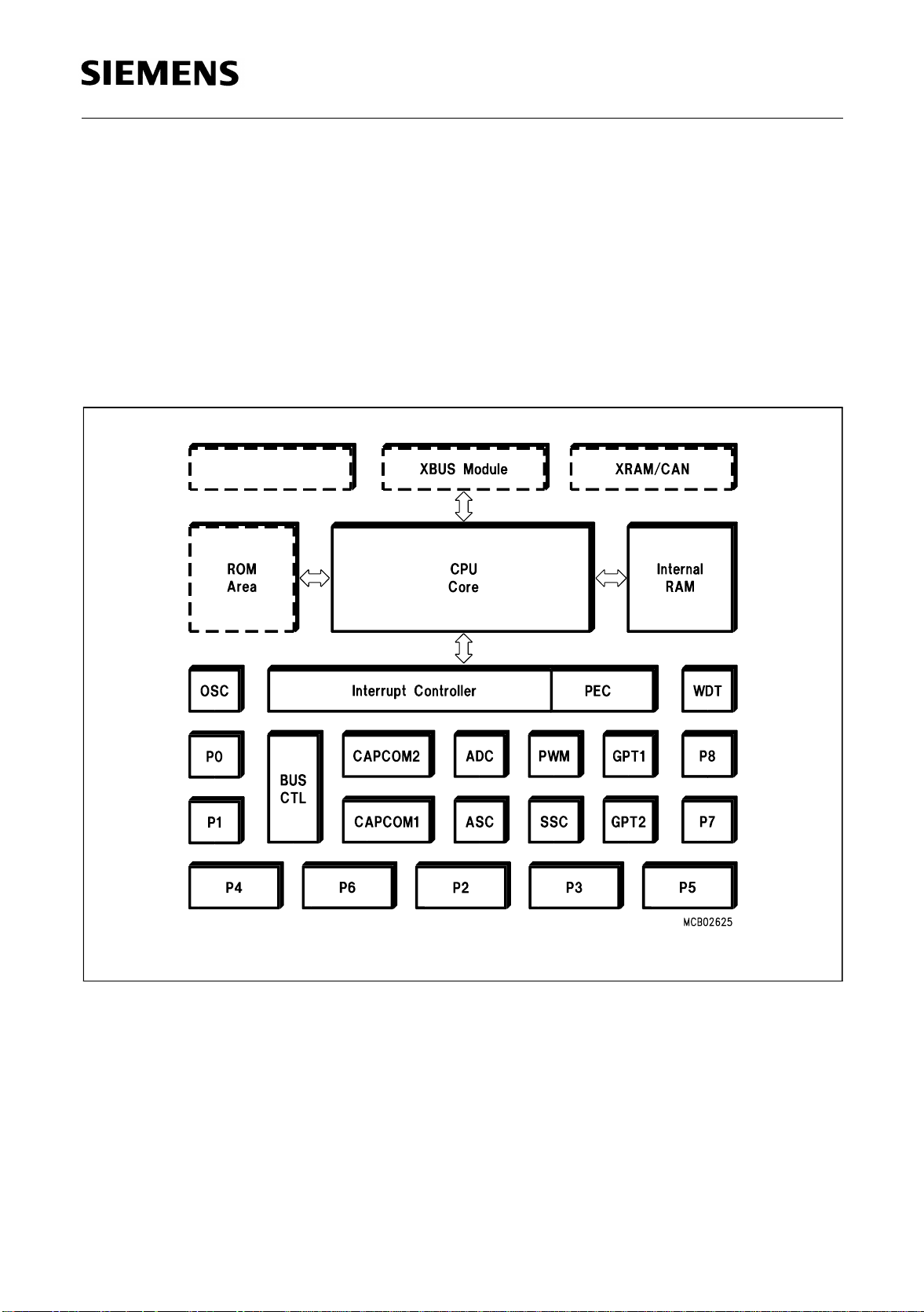
Figure 2-1
C167 Functional Block Diagram
Semiconductor Group 2-1

Architectural Overview / C167
2.1 Basic CPU Concepts and Optimizations
The main core of the CPU cons ists of a 4-stage ins truction pipeline, a 16-bi t arithmetic and logic unit
(ALU) and dedicated SFRs. Additional hardware is provided for a separate multiply and divide unit,
a bit-mask generator and a barrel shifter.
Figure 2-2
CPU Block Diagram
To meet the demand for greater performance and flexibility, a number of areas has been optimized
in the processor core. Functional blocks in the CPU core are controlled by signals from the
instruction decode logic. These are summarized below, and described in detail in the following
sections:
1) High Instruction Bandwidth / Fast Execution
2) High Function 8-bit and 16-bit Arithmetic and Logic Unit
3) Extended Bit Processing and Peripheral Control
4) High Performance Branch-, Call-, and Loop Processing
5) Consistent and Optimized Instruction Formats
6) Programmable Multiple Priority Interrupt Structure
Semiconductor Group 2-2

Architectural Overview / C167
High Instruction Bandwidth / Fast Execution
Based on the hardware provisions, most of the C167’s instructions can be executed in just one
machine cycle, which requires 100 ns at 20 MHz CPU clock. For example, shift and rotate
instructions are always processed within one machine cycle, independent of the number of bits to
be shifted.
Branch-, multiply- and divide instructions normally take more than one machine cycle. These
instructions, however, have also been optimized. For example, branch instructions only require an
additional machine cycle, when a branch is taken, and most branches taken in loops require no
additional machine cycles at all, due to the so-called ‘Jump Cache’.
A 32-bit / 16-bit division takes 1µs, a 16-bit
The instruction cycle time has been dramatically reduced through the use of instruction pipelining.
This technique allows the core CPU to process portions of multiple sequential ins tructi on stages in
parallel. The following four stage pipeline provides the optimum balancing for the CPU core:
FETCH: In this stage, an instruction is fetched from the internal ROM or RAM or from the external
memory, based on the current IP value.
16-bit multiplication takes 0.5 µs.
*
DECODE: In this stage, the previously fetched instruction is decoded and the required operands
are fetched.
EXECUTE: In this stage, the specified operation is performed on the previously fetched operands.
WRITE BACK: In this stage, the result is written to the specified location.
If this technique were not used, each instruction would require four machine c ycles. Th is increas ed
performance allows a greater number of tasks and interrupts to be processed.
Instruction Decoder
Instruction decoding is primarily generated from PLA outputs based on the selected opcode. No
microcode is used and each pi peline stag e receives contro l signals sta ged in control regis ters from
the decode stage PLAs. Pipeline holds are primarily caused by wait states for external memory
accesses and cause the holding of signals in the control registers. Multiple-cycle instructions are
performed through instruction injection and simple internal state machines which modify required
control signals.
High Function 8-bit and 16-bit Arithmetic and Logic Unit
All standard arithmetic and logical operations are performed in a 16-bit ALU. In addition, for byte
operations, signals are provided from bits six and seven of the ALU result to correctly set the
condition flags. Multiple precision arithmetic is provided through a 'CARRY-IN' signal to the ALU
from previously calculated portions of the desired operation. Most internal execution blocks have
been optimized to perform operations on either 8-bit or 16-bit quanti ties. Once the pipeline has been
filled, one instruction is completed per machine cycle, except for multiply and divide. An advanced
Booth algorithm has been incorporated to allow four bits to be multiplied and two bits to be divided
per machine cycle. Thus, these operations use two coupled 16-bit registers, MDL and MDH, and
require four and nine machine cycles, respective ly, to perform a 16-bit by 16-bit (or 32-bit by 16-bit)
calculation plus one machine cycle to setup and adjust the operands and the result. Even these
Semiconductor Group 2-3

Architectural Overview / C167
longer multiply and divide instructions can be interrupted during their executi on to allow for very fast
interrupt response. Instructions have also been provided to allow byte packing in memory while
providing sign extension of bytes for word wide arithmetic operations. The internal bus structure
also allows transfers of bytes or words to or from peripherals based on the p eripheral requirements.
A set of consistent flags is automati call y upda ted in the PSW after each arithmetic, logical, shift, or
movement operation. These flags allow branching on specific conditions. Support for both signed
and unsigned arithmetic is provided through user-specifiable branch tests. These flags are also
preserved automatically by the CPU upon entry into an interrupt or trap routine.
All targets for branch calculations are also computed in the central ALU.
A 16-bit barrel shifter provides multiple bit shifts in a single cycle. Rotates and arithmetic shifts are
also supported.
Extended Bit Processing and Peripheral Control
A large number of instructions has been dedicated to bit processing. These instructions provide
efficient control and testing of peripherals while enhancing data manipulation. Unlike other
microcontrollers, these instructions provide direct access to two operands in the bit-addressable
space without requiring to move them into temporary flags.
The same logical instruc tions ava ilabl e for words and bytes are also supported for bi ts. This allows
the user to compare and modify a control bit for a peripheral in one instruction. Multiple bit shift
instructions have been included to avoid long instruction streams of single bit shift operations.
These are also performed in a single machine cycle.
In addition, bit field instructions have been provided, which allow the modification of multiple bits
from one operand in a single instruction.
High Performance Branch-, Call-, and Loop Processing
Due to the high percentage of branching in controller applications, branch instructions have been
optimized to require one extra machine cycle only when a branch is taken. This is implemented by
precalculating the target address while decoding the instruction. To decrease loop execution
overhead, three enhancements have been provided:
• The first solution provides single cycl e branch execution after the first iteration of a loop. Thus , only
one machine cycle is lost during the execution of the entire loop. In loops which fall through upon
completion, no machine cycles are lost when exiting the loop. No special instructions are required
to perform loops, and loops are automatically detected during execution of branch instructions.
• The second loop enhancement allows the detection of the end of a table and avoids the use of two
compare instructions embedded in loops. One simply places the lowest negati ve number at the end
of the specific table, and s pecifies branching i f neither this value nor the compared value have been
found. Otherwise the loop is terminated if either conditi on has been met. The terminating condition
can then be tested.
• The third loop enhancement provides a more flexible solution than the Decrement and Skip on
Zero instruction which is found in other microcontrollers. Through the use of Compare and
Increment or Decrement instructions, the user can make comparisons to any v alue. This allows loop
counters to cover any range. This is particularly advantageous in table searching.
Semiconductor Group 2-4

Architectural Overview / C167
Saving of system state is automatically performed on the internal system stack avoiding the use of
instructions to preserve state upon entry and exit of interrupt or trap routi nes. Call instructions push
the value of the IP on the system s tack, and require the same executi on time as branch instru ctions.
Instructions have also be en p rovide d to su pport indirec t b ra nch and cal l i nstruct ions. Thi s suppo rts
implementation of multiple CASE statement branching in assembler macros and high level
languages.
Consistent and Optimized Instruction Formats
To obtain optimum performance in a pipelined design, an instruction set has been designed which
incorporates concepts from Reduced Instruction Set Computing (RISC). These concepts primarily
allow fast decoding of the instructi ons and operands while reducing pi peline holds. These concepts,
however, do not preclude the use of complex instructions, which are required by microcontroller
users. The following goals were used to design the instruction set:
1) Provide powerful instructions to perform operations which currently require sequences of
instructions and are frequently used. Avoid transfer into and out of temporary registers such
as accumulators and carry bits. Perform tasks in parallel such as saving state upon entry into
interrupt routines or subroutines.
2) Avoid complex encoding schemes by placing operands in consistent fields for each instruction. Also avoid complex addressing modes which are not frequently used. This decreases
the instruction decode time while also simplifying the development of compilers and assemblers.
3) Provide most frequently used instructions with one-word instruc tion formats . All other ins tructions are placed into two-word formats. This allows all instructions to be placed on word
boundaries, which alleviates the need for complex alignment hardware. It also has the benefit of increasing the range for relative branching instructions.
The high performance offered by the hardware implementation of the CPU can efficie ntly be utilized
by a programmer via the highly functional C167 instruction set which includes the following
instruction classes:
• Arithmetic Instructions
• Logical Instructions
• Boolean Bit Manipulation Instructions
• Compare and Loop Control Instructions
• Shift and Rotate Instructions
• Prioritize Instruction
• Data Movement Instructions
• System Stack Instructions
• Jump and Call Instructions
• Return Instructions
• System Control Instructions
• Miscellaneous Instructions
Possible operand types are bits, bytes and words. Specific instruction support the conversion
(extension) of bytes to words. A variety of direct, indirect or immediate addressing modes are
provided to specify the required operands.
Semiconductor Group 2-5

Architectural Overview / C167
Programmable Multiple Priority Interrupt System
The following enhancements have been included to allow processing of a large number of interrupt
sources:
1) Peripheral Event Controller (PEC): This processor is used to off-loa d many interrupt requests
from the CPU. It avoids the overhead of entering and exiting interrupt or trap routi nes by pe rforming single-cycle interrupt-driven byt e or word data transfers between any two locations in
segment 0 with an optional increment of either the PEC source or the destination pointer.
Just one cycle is ’stolen’ from the current CPU activity to perform a PEC service.
2) Multiple Priority Interrupt Controller: This controller allows all interrupts to be placed at any
specified priority. Interrupts may also be grouped, which provides the user with the ability to
prevent similar priority tasks from interrupting each other. For each of the possible interrupt
sources there is a separate control register, which contains an interrupt request flag, an interrupt enable flag and an interrupt priority bitfi eld. O nce havi ng been acc epted by the CPU, an
interrupt service can only be interrupt ed by a h igher prioritized service request. For standard
interrupt processing, each of the possible interrupt sources has a dedicated vector location.
3) Multiple Register Banks: This feature allows the user to specify up to sixteen general pur-
pose registers located anywhere i n the inte rnal RAM. A sin gle one-machine-cycl e instruct ion
allows to switch register banks from one task to another.
4) Interruptable Multiple Cycle Instructions: Reduced interrupt latency is provided by allowing
multiple-cycle instructions (multiply, divide) to be interruptable.
With an interrupt response time within a range from just 250 ns to 500 ns (in case of internal
program execution), the C167 is capable of reacting very fast on non-deterministic events.
Its fast external interrupt inputs are sampled every 50 ns and allow to recognize even very short
external signals.
The C167 also provides an excellent mechanism to identify and to process exceptions or error
conditions that arise during run-time, so called ’Hardware Traps’. Hardware traps cause an
immediate non-maskable system reaction which is similiar to a standard interrupt service
(branching to a dedicated vector table location). The occurrence of a hardware trap is additionally
signified by an individual bit in the trap flag register (TFR). Except for another higher prioritize d trap
service being in progress, a hardware trap will interrupt any current program execution. In turn,
hardware trap services can normally not be interrupted by standard or PEC interrupts.
Software interrupts are supported by means of the ’TRAP’ instruction in combination with an
individual trap (interrupt) number.
Semiconductor Group 2-6

Architectural Overview / C167
2.2 The On-chip System Resources
The C167 controllers provide a number of powerful system resources designed around the CPU.
The combination of CPU and these resources results in the high performance of the members of
this controller family.
Peripheral Event Controller (PEC) and Interrupt Control
The Peripheral Event Controller allows to respond to an interrupt request with a single da ta transfer
(word or byte) which only consumes one instruction cycle and do es not require to sa ve and restore
the machine status. Each interrupt source is prioritized every mac hine cy cle in the interrupt con trol
block. If PEC service is selected, a PEC transfer is started. If CPU interrupt service is requested, the
current CPU priority level stored in the PSW register is tested to determine whether a higher priority
interrupt is currently being serviced. When an interrupt is acknowledged, the current state of the
machine is saved on the inte rnal syst em stack and the CPU branches to the sy stem spec ific vec tor
for the peripheral.
The PEC contains a set of SFRs which store the count value a nd control bits for eight data trans fer
channels. In addition, the PEC uses a dedicated area of RAM which contains the source and
destination addresses. The PEC is controlled similar to any other peripheral through SFRs
containing the desired configuration of each channel.
An individual PEC transfer counter is implicitly decremented for each PEC service except forming
in the continuous transfer mode. When this counter reaches zero, a standard interrupt is performed
to the vector location related to the corresponding source. PEC services are very well suited, for
example, to move register contents to/from a memory table. The C167 has 8 PEC channels each
of which offers such fast interrupt-driven data transfer capabilities.
Memory Areas
The memory space of the C167 is configured in a Von Neumann architecture which means that
code memory, data memory, registers and IO ports are organized within the same linear address
space which covers up to 16 MBytes. The entire memory space can be accessed bytewise or
wordwise. Particular portions of the on-chip memory have additionally been made directly bit
addressable.
A 2 KByte 16-bit wide internal RAM provides fast access to General Purpose Registers (GPRs),
user data (variables) and system stack. The internal RAM may also be used for code. A unique
decoding scheme provides flexible user register banks in the internal memory while optimizing the
remaining RAM for user data.
The CPU disposes of an actual register context consisting of up to 16 wordwide and/or bytewide
GPRs, which are physically located within the on-chip RAM area. A Context Pointer (CP) register
determines the base address of the active register bank to be acces sed by the CPU at a time. The
number of register banks is only re stricted by the available internal RAM s pace. For easy parameter
passing, a register bank may overlap others.
A system stack of up to 1024 words is provi ded as a s torage fo r temporary data. The sy stem stack
is also located within the on-chip RAM area, and it is accessed by the CPU via the stack p ointer (SP)
register. Two separate SFRs, STKOV and STKUN, are implicitly compared against the stack
pointer value upon each stack access for the detection of a stack overflow or underflow.
Semiconductor Group 2-7

Architectural Overview / C167
Hardware detection of the selected memory space is placed at the internal memory decoders and
allows the user to specify any address directly or ind irectly and obtain the desired data without using
temporary registers or special instructions.
A 2 KByte 16-bit wide on-chip XRAM provides fast access to user data (variables), user stacks
and code. The on-chip XRAM is realized as an X-Peripheral and appears to the software as an
external RAM. Therefore it cannot store register banks and is not bitaddressable. The XRAM allows
16-bit accesses with maximum speed.
An optional internal ROM provides for both code and consta nt dat a storage. Th is memory area is
connected to the CPU via a 32-bit-wide bus. Thus, an entire do uble-word instruction can be f etched
in just one machine cycle. Program execution from the on-chip ROM is the fastest of all possible
alternatives.
For Special Function Registers 1024 Bytes of the address space are reserved. The standard
Special Function Register area (SFR) uses 512 bytes, while the Extended Special Function
Register area (ESFR) uses the other 512 bytes. (E)SFRs are wordwide registers which are used for
controlling and monitoring functions of the different on-chip units. Unused (E)SFR addresses are
reserved for future members of the C167 family with enhanced functionality.
External Bus Interface
In order to meet the needs of designs where more memory is required than is provided on ch ip, up
to 16 MBytes of external RAM and/or ROM can be connected to the microcontrol ler v ia i ts ex ternal
bus interface. The integrated External Bus Contro ller (EBC) allows to access external memory and/
or peripheral resources in a very flexible way. For up to five address areas the bus mode
(multiplexed / demultiplexed), the data bus width (8-bit / 16-bit) and even the length of a bus cycle
(waitstates, signal delays) can be selected independently. This allows to access a variety of
memory and peripheral components directly and with maximum efficiency. If the device does not
run in Single Chip Mode, where no external memory is required, the EBC can control external
accesses in one of the following four different external access modes:
• 16-/18-/20-/24-bit Addresses, 16-bit Data, Demultiplexed
• 16-/18-/20-/24-bit Addresses, 8-bit Data, Demultiplexed
• 16-/18-/20-/24-bit Addresses, 16-bit Data, Multiplexed
• 16-/18-/20-/24-bit Addresses, 8-bit Data, Multiplexed
The demultiplexed bus modes use PORT1 for addresses and PORT0 for data input/output. The
multiplexed bus modes use PORT0 for both addresses and data input/ou tput. All modes u se Port 4
for the upper address lines (A16...) if selected.
Important timing characteristics of the external bus interface (waitstates, ALE length and Read/
Write Delay) have been made programmable to allow the user the adaption of a wide range of
different types of memories and/or peripherals. Access to very slow memories or peripherals is
supported via a particular 'Ready' function.
For applications which require less than 64 KBytes of address space, a non-segmented memory
model can be selected, where all locations can be addressed by 16 bits, and thus Port 4 is not
needed as an output for the upper address bits (A23/A19/A17...A16), as is the case when using the
segmented memory model.
Semiconductor Group 2-8
Architectural Overview / C167
The on-chip XBUS is an internal representation of the external bus and allows to access
integrated application-specific peripherals/modules in the same way as external components. It
provides a defined interface for these customized peripherals.
The on-chip XRAM and the on-chip CAN-Module are examples for these X-Peripherals.
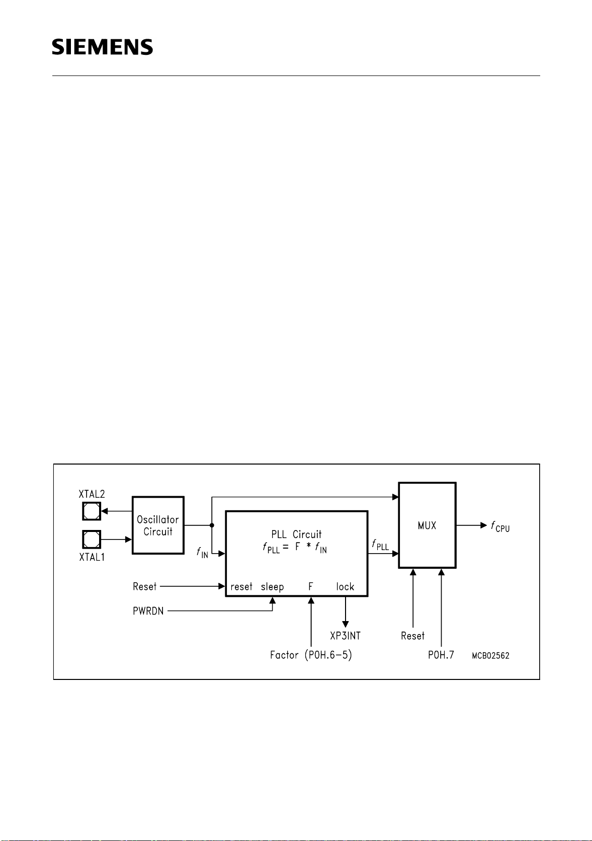
Clock Generator
The on-chip clock generator provides the C167 with its basic clock signal that controls all activities
of the controller hardware. Its oscillator can either run with an external crystal and appropriate
oscillator circuitry (see also recommendations in chapter „Dedicated Pins“) or it can be driven by an
external oscillator. The oscillator either directly feeds the external clock signal to the controller
hardware (through buffers, of course), divides the external cl ock frequency by 2, or feeds an on-chip
phase locked loop (PLL) which multiplies the input frequency by a selectable factor F (depending on
the device mode and/or type). This resulting internal clock signal is also referred to as “CPU clock”.
Two separated clock signals are generated for the CPU itself and the peripheral part of the chip.
While the CPU clock is stopped during the idle mode, the peripheral clock keeps running. Both
clocks are switched off, when the power down mode is entered.
The on-chip PLL circuit allows operation of the C167 on a low frequency external clock while still
providing maximum performance. The PLL multiplies the external clock frequency by a selectable
factor of 1:F and generates a CPU clock signal with 50% duty cycle. The PLL als o provides fail safe
mechanisms which allow the detection of frequency deviations and the execution of emergency
actions in case of an external clock failure.
Figure 2-3
PLL Block Diagram
Semiconductor Group 2-9

Architectural Overview / C167
PLL Operation
The PLL is enabled when pin P0H.7 is latched high during reset. On power-up the PLL provides a
stable clock signal within ca. 1 ms after V
signal (in this case the PLL will run on its basic frequency of 2...5 MHz). The PLL starts
synchronizing with the external clock signal as soon as it is available. Within ca. 1 ms after stable
oscillations of the external clock within the specified frequency range the PLL will be synchronous
with this clock at a frequency of F *f
OSC
Note: If the C167 is required to operate on the desired CPU clock directly after reset make sure that
RSTIN
remains active until the PLL has locked (ca. 1 ms).
When PLL operation is selected the CPU clock is a selectable multiple of the oscillator frequency,
ie. the input frequency. The table below lists the possible selections.
has reached 5V±10%, even if there is no external clock
CC
, ie. the PLL locks to the external clock.
P0.15-13
(P0H.7-5)
111
110
101
100
0XX
1)
The external clock input range refers to a CPU clock range of 10...25 MHz.
2)
The maximum depends on the duty cycle of the external clock signal.
CPU
Frequency f
= f
* F
XTAL
f
* 4 2.5 to 6.25 MHz Default configuration
XTAL
f
* 3 3.33 to 8.33 MHz
XTAL
f
* 2 5 to 12.5 MHz
XTAL
f
* 5 2 to 5 MHz
XTAL
f
* 1 1 to 25 MHz Direct drive
XTAL
CPU
External Clock Input
Range
1)
Notes
2)
In emulation mode direct drive is selected with P0.15 (P0H.7) = ’1’.
The PLL constantly synchronizes to the external clock signal. Due to the fact that the external
frequency is 1/F’th of the PLL output frequency the outpu t frequency may be slightly higher or lower
than the desired frequency. This jitter is irrelevant for longer time periods. For short periods (1...4
CPU clock cycles) it remains below 4%.
When the PLL detects a missing input clock signal it generates an interrupt request. This warning
interrupt indicates that the PLL frequency is no more locked, ie. no more stable. This occurs when
the input clock is unstabl e and es pecially when the i nput cloc k fails complete ly, eg. due to a broken
crystal. In this case the synchronization mechanism will reduce the PLL output frequency down to
the PLL’s basic frequency (2...5 MHz). The basic frequency is still gene rated and allows the CPU to
execute emergency actions in case of a loss of the external clock.
Operation without PLL
The PLL is disabled when pin P0H.7 is latched low during reset. In this case the C167’s clock
system is directly fed from the external clock input, ie. f
OSC
= f
. The maximum input clock
CPU
frequency depends on the clock signal’s duty cycle, because the minimum values for the clock
phases (TCLs) must be respected.
Semiconductor Group 2-10

Architectural Overview / C167
2.3 The On-chip Peripheral Blocks
The C167 family clearly separates peripherals from the core. This structure permits the maximum
number of operations to be performed in p arallel and allows peripherals to be added or deleted from
family members without modifications to the core. Each functional block processes data
independently and communicates information over common buses. Peripherals are controlled by
data written to the respective Special Function Registers (SFRs). These SFRs are located either
within the standard SFR area (00’FE00
(00’F000
...00’F1FFH).
H
These built in peripherals either allow the CPU to interface with the external world, or provide
functions on-chip that otherwise were to be added externally in the respective system.
The C167 generic peripherals are:
• Two General Purpose Timer Blocks (GPT1 and GPT2)
• Two Serial Interfaces (ASC0 and SSC)
• A Watchdog Timer
• Two 16-channel Capture / Compare units (CAPCOM1 and CAPCOM2)
• A 4-channel Pulse Width Modulation unit
• A 10-bit Analog / Digital Converter
• Nine IO ports with a total of 111 IO lines
...00’FFFFH) or within the extended ESFR area
H
Each peripheral also contains a set of Special Function Registers (SFRs), which control the
functionality of the peripheral and temporarily store intermediate data results. Each peripheral has
an associated set of status flags. Individually selected clock signals are generated for each
peripheral from binary multiples of the CPU clock.
Peripheral Interfaces
The on-chip peripherals generally have two different types of interfaces, an interface to the CPU
and an interface to external hardware. Communica tion between CPU and peripherals i s performed
through Special Function Registers (SFRs) and interrupts. The SFRs serve as control/status and
data registers for the peripherals. Interrupt requests are generated by the peripherals based on
specific events which occur during their operation (eg. operation complete, error, etc.).
For interfacing with external hardware, speci fic pins of the paral lel ports a re used, when an input or
output function has been selected for a peripheral. During this time, the port pins are controlled by
the peripheral (when used as outputs) or by the external hardware which controls the peripheral
(when used as inputs). This is called the 'alternate (input or output) function' of a port pin, in contrast
to its function as a general purpose IO pin.
Peripheral Timing
Internal operation of CPU and peripherals is based on the CPU clock (f
). The on-chip oscillator
CPU
derives the CPU clock from the crystal or from the external clock signal. The clock signal which is
gated to the peripherals is independent from the clock signal which feeds the CPU. During Idle
mode the CPU’s clock is stopped while the peripherals continue their operation. Peripheral SFRs
may be accessed by the CPU once per state. When an SFR is written to by software in the same
state where it is also to be modified by the peripheral, the software write operation has priority.
Further details on peripheral timing are included in the specific sections about each peripheral.
Semiconductor Group 2-11

Architectural Overview / C167
Programming Hints
Access to SFRs
All SFRs reside in data page 3 of the memory space. The following addressing mechanisms allow
to access the SFRs:
• indirect or direct addressing with 16-bit (mem) addresses it must be guaranteed that the used
data page pointer (DPP0...DPP3) selects data page 3.
• accesses via the Peripheral Event Controller (PEC) use the SRCPx and DSTPx pointers instead
of the data page pointers.
• short 8-bit (reg) addresses to the standard SFR area do not use the data page pointers but
directly access the registers within this 512 Byte area.
• short 8-bit (reg) addresses to the extended ESFR area require switching to the 512 Byte
extended SFR area. This is done via the EXTension instructions EXTR, EXTP(R), EXTS(R).
Byte write operations to word wide SFRs via indirect or direct 16-bit (mem) addressing or byte
transfers via the PEC force zeros in the non-addressed byte. Byte write operations via short 8-bit
(reg) addressing can only access the low byte of an SFR and force zeros in the high byte. It is
therefore recommended, to use the bit field instructions (BFLDL and BFLDH) to write to any number
of bits in either byte of an SFR without disturbing the non-addressed byte and the unselected bits.
Reserved Bits
Some of the bits which are contained in the C167's SFRs are marked as 'Reserved'. User so ftware
should never write '1's to reserved bits. These bits are c urrently not impl emented and may be used
in future products to invoke new functions. In this case, the active state for these functions will be
'1', and the inactive state will be '0'. Therefore writing only ‘0’s to reserved locations provides
portability of the current software to future devices. Read accesses to reserved bits return ‘0’s.
Parallel Ports
The C167 provides up to 111 IO lines which are organized into eight input/output ports and one
input port. All port lines are bit-addressable, and all input/output lines are individually (bit-wise)
programmable as inputs or outputs via direction registers. The IO ports are true bidirectional ports
which are switched to high impedance state when configured as inp uts. The output drivers of three
IO ports can be configured (pin by pin) for push/pull operation or open-drain operation via control
registers. During the internal reset, all port pins are configured as inputs.
All port lines have programmable alternate input or output functions associated with them. PORT0
and PORT1 may be used as address and data lines when accessing ex ternal memory, while Port 4
outputs the additional segment address bits A23/19/17...A16 in systems where segmentation is
used to access more than 64 KBytes of memory. Port 6 provides optional bus arbitration signals
(BREQ
provides inputs/outputs for the CAPCOM1 unit. Port 3 includes alternate functions of timers, serial
interfaces, the optional bus control signal BHE
used for timer control signals and for the analog inputs to the A/D Converter. Port 7 provides the
output signals from the PWM unit and inputs/outputs for the CAPCOM2 unit. Port 8 provides inputs/
outputs for the CAPCOM2 unit. Fo ur pins o f PORT1 may also be used as inputs f or the CAPCOM2
unit. All port lines that are not used for these alternate functions may be used as general purpose
IO lines.
, HLDA, HOLD) and chip select signals. Port 2 accepts the fas t external int errupt inputs and
and the system clock output (CLKOUT). Port 5 is
Semiconductor Group 2-12

Architectural Overview / C167
Serial Channels
Serial communication with other microcontrollers, processors, terminals or external peripheral
components is provided by two serial interfaces with different functionality, an Asynchronous/
Synchronous Serial Channel (ASC0) and a High-Speed Synchronous Serial Channel (SSC).
They are upward compatible with the serial ports of the Siemens 8-bit microcontroller families and
support full-duplex asynchronous communica tion at up to 625 KBaud and half-duplex sy nchronous
communication at up to 5 MBaud (2.5 MBaud on the ASC0) @ 20 MHz CPU clock. The SSC may
be configured so it interfaces with serially linked peripheral components.
Two dedicated baud rate generators allow to set up a ll standard baud rates with out oscillator tuning.
For transmission, reception and error handling 3 separate interrupt vecto rs are provided on channel
SSC, 4 vectors are provided on channel ASC0.
In asynchronous mode, 8- or 9-bit data frames are transmitted or received, preceded by a start bit
and terminated by one or two stop bits. For multiprocessor communication, a mechanism to
distinguish address from data bytes has been included (8-bit data plus wake up bit mode).
In synchronous mode, the ASC0 transmits or receives bytes (8 bits) synchronously to a shift clock
which is generated by the ASC0. The SSC transmits or receives characters of 2...16 bits length
synchronously to a shift clock which can be generated by the SSC (master mode) or by an extern al
master (slave mode). The SSC can start shifting with the LSB or with the MSB, while the ASC0
always shifts the LSB first.
A loop back option is available for testing purposes.
A number of optional hardware error detection capabilities has been included to increase the
reliability of data transfers. A parity bit can automatically be generated on transmission or be
checked on reception. Framing error detection allows to recognize data frames with missing stop
bits. An overrun error will be generated, if the last character received has not been read out of the
receive buffer register at the time the reception of a new character is complete.
The On-chip CAN Module
The integrated CAN Module handles the completely autonomous transmission and reception of
CAN frames in accordance with the CAN specification V2.0 part B (active), ie. the on-chip
CAN M odule can receive and transmit standard frames with 11-bit identifiers as well as extended
frames with 29-bit identifiers.
The module provides Full CAN functionality on up to 15 message objects. Messag e object 15 may
be configured for Basic CAN functionality. Both modes provide separate masks for acceptance
filtering which allows to accept a number of identifiers in Ful l CAN mode and also allows to disregard
a number of identifiers in Basic CAN mode. All message objects can be updated independe nt from
the other objects and are equipped for the maximum message length of 8 bytes.
The bit timing is derived from the XCLK and is programmable up to a data rate of 1 MBaud. The
CAN Module uses two pins to interface to a bus transceiver.
Note: The CAN Module is not part of all C167 derivatives. This description, of course, refers to
those devices only which incorporate a CAN Module.
Semiconductor Group 2-13

Architectural Overview / C167
General Purpose Timer (GPT) Unit
The GPT units represent a very flexible multifunctional timer/counter structure which may be used
for many different time related tasks such as event timing and co unting, pulse width and duty cy cle
measurements, pulse generation, or pulse multiplication.
The five 16-bit timers are organiz ed in two separate m odules, GPT1 and G PT2. Each ti mer in each
module may operate independently in a number of different modes, or may be concatenated with
another timer of the same module.
Each timer can be configured individually for one of three basic modes of operation, which are
Timer, Gated Timer, and Counter Mode. In Timer Mode the input clock for a timer is derived from
the internal CPU clock divided by a programmable p resca ler, while Counter Mode a llows a timer to
be clocked in reference to external events (via TxIN).
Pulse width or duty cycle measurement is supported in Gated Timer Mode where the operation of
a timer is controlled by the ‘gate’ level on its external input pin TxIN.
The count direction (up/down) for each timer is programmable by software or may additionally be
altered dynamically by an external signal (TxEUD) to facilitate eg. position tracking.
The core timers T3 and T6 have output toggle latches (TxOTL) which change their state on each
timer over-flow/underflow. The state o f these latches may be output on port pins (TxOUT) or may be
used internally to concat enate the core timers with the respective a uxiliary timers resultin g in 32/33bit timers/counters for measuring long time periods with high resolution.
Various reload or capture functions can be selected to reload timers or capture a timer’s contents
triggered by an external signal or a selectable transition of toggle latch TxOTL.
The maximum resolution of the timers in module GPT1 is 400 ns (@ 20 MHz CPU clock). With its
maximum resolution of 200 ns (@ 20 MHz CPU clock) the GPT2 timers provide precise event
control and time measurement.
Watchdog Timer
The Watchdog Timer represents one of the fail-safe mechani sms which have been implemented to
prevent the controller from malfunctioning for longer periods of time.
The Watchdog Timer is always en abled after a reset of the chip, and can only be disabled in the time
interval until the EINIT (en d of initial ization) ins truction has been executed. Thus , the chip’ s start-up
procedure is always monitored. The software has to be designed to service the Watchdog Timer
before it overflows. If, due to hardware or software related failures, the software fails to do so, the
Watchdog Timer overflows and generates an internal ha rdware reset and pulls the RSTOUT
in order to allow external hardware components to reset.
pin low
The Watchdog Timer is a 16-bit timer, clocked with the CPU clock divided either by 2 or by 128. The
high byte of the Watchdog Timer register can be set to a prespecified reload value (stored in
WDTREL) in order to allow further variation of the monitored time interval. Each time it is serviced
by the application software, the high byte of the Watchdog Timer is reloaded. Thus, time intervals
between 25 µs and 420 ms can be monitored (@ 20 MHz). The default Watchdog Timer interval
after reset is 6.55 ms (@ 20 MHz).
Semiconductor Group 2-14

Architectural Overview / C167
Capture/Compare (CAPCOM) Units
The two CAPCOM units support generation and control of timing sequences on up to 32 channels
with a maximum resolution of 400 ns. The CAPCOM units are typically used to handle high speed
IO tasks such as pulse and wa veform generati on, pulse widt h modulation (PWM), Digital to Anal og
(D/A) conversion, software timing, or time recording relative to external events.
Four 16-bit timers (T0/T1, T7/T8) with reload registers provide two independent time bases for the
capture/compare register array.
The input clock for the timers is programmable to several prescaled values of the internal CPU
clock, or may be derived from an overflow/underflow of timer T6 in module GPT2. This provides a
wide range of variation for the timer period and resolution and allows precise adjustments to the
application specific requiremen ts. In additi on, ex ternal c ount i nputs for CAPCOM time rs T0 an d T7
allow event scheduling for the capture/compare registers relative to external events.
Both of the two capture/compare register arrays contain 16 dual purpose capture/compare
registers, each of which may be individually allocated to either CAPCOM timer T0 or T1 (T7 or T8,
respectively), and programmed for capture or compare function. Each register has one port pin
associated with it which serves as an i nput pin for triggering the capture function, or as an output pin
(except for CC24...CC27) to indicate the occurence of a compare event.
When a capture/compare register has been selected for capture mode, the current contents of the
allocated timer will be latched (captured) into the capture/compare register in response to an
external event at the port pin which is associated with this register. In addition, a specific interrupt
request for this capture/compare register is generated. Either a positive, a negative, or both a
positive and a negative external sign al trans ition at the pi n can be selected as the triggering event.
The contents of all registers which have been selected for one of the five compare modes are
continuously compared with the contents of the allocated timers. When a match occurs between the
timer value and the value in a capt ure/compare regi ster, specific acti ons wil l be take n based on the
selected compare mode.
Pulse Width Modulation Unit
The PWM Unit supports the generation of up to four independent high-spee d PWM signals. It allows
to generate standard (edge aligned) PWM signals as well as symmetrical (center aligned) PWM
signals. In Burst Mode two chann els may be comb ined wi th their out put signal s ANDed, where one
channel gates the output signal of the other channel. Single Shot Mode allows to generate single
output pulses (retriggerable) under software control. Each PWM channel is controlled by an up/
down counter with associated reload and compare regis ters. The polarity of the PWM output signals
may be controlled via the respective port output latch (combination via EXOR).
Semiconductor Group 2-15

Architectural Overview / C167
A/D Converter
For analog signal measurement, a 10-bit A/D converter with 16 multiplexed input channels and a
sample and hold circuit has been integrated on-chip. It uses the method of successive
approximation. The sample time (for loading the capacitors) and the conversion time is
programmable and can so be adjusted to the external circuitry.
Overrun error detection/protection is provided for the conversion result register (ADDAT): either an
interrupt request will be generated when the result of a previous conversion has not b een read from
the result register at the time the next conversion is complete, or the next conversi on is suspended
in such a case until the previous result has been read.
For applications which require l ess than 16 analog input channel s, the remaining channel inputs can
be used as digital input port pins.
The A/D converter of the C167 supports four different conversion modes. In the standard Single
Channel conversion mode, the analog level on a specified channel is sampled onc e and converted
to a digital result. In the Single Channel Continuous mode, the analog level on a specified channel
is repeatedly sampled and converted without software intervention. In the Auto Scan mode, the
analog levels on a prespecified number of channels are seque ntially sampled and converted. In the
Auto Scan Continuous mode, the number of prespecified channels is repeatedly sampled and
converted. In addition, the conversion of a specific channel can be inserted (injected) into a running
sequence without disturbing this sequence. This is called Channel Injection Mode.
The Peripheral Event Controller (PEC) may be used to automatically store the conversion results
into a table in memory for later evaluation, without requiring the overhead of entering and exiting
interrupt routines for each data transfer.
Semiconductor Group 2-16

Architectural Overview / C167
2.4 Protected Bits
The C167 provides a special mechanism to protect bits which can be modified by the on-chip
hardware from being changed unintentionally by software accesses to related bit s (see also chapter
“The Central Processing Unit”).
The following bits are protected:
Register Bit Name Notes
T2IC, T3IC, T4IC T2IR, T3IR, T4IR GPT1 timer interrupt request flags
T5IC, T6IC T5IR, T6IR GPT2 timer interrupt request flags
CRIC CRIR GPT2 CAPREL interrupt request flag
T3CON, T6CON T3OTL, T6OTL GPTx timer output toggle latches
T0IC, T1IC T0IR, T1IR CAPCOM1 timer interrupt request flags
T7IC, T8IC T7IR, T8IR CAPCOM2 timer interrupt request flags
S0TIC, S0TBIC S0TIR, S0TBIR ASC0 transmit(buffer) interrupt request flags
S0RIC, S0EIC S0RIR, S0EIR ASC0 receive/error interrupt request flags
S0CON S0REN ASC0 receiver enable flag
SSCTIC, SSCRIC SSCTIR, SSCRIR SSC transmit/receive interrupt request flags
SSCEIC SSCEIR SSC error interrupt request flag
SSCCON SSCBSY SSC busy flag
SSCCON SSCBE, SSCPE SSC error flags
SSCCON SSCRE, SSCTE SSC error flags
ADCIC, ADEIC ADCIR, ADEIR ADC end-of-conv./overrun intr. request flag
ADCON ADST, ADCRQ ADC start flag / injection request flag
CC31IC...CC16IC CC31IR...CC16IR CAPCOM2 interrupt request flags
CC15IC...CC0IC CC15IR...CC0IR CAPCOM1 interrupt request flags
PWMIC PWMIR PWM module interrupt request flag
TFR TFR.15,14,13 Class A trap flags
TFR TFR.7,3,2,1,0 Class B trap flags
P2 P2.15...P2.0 All bits of Port 2
P7 P7.7...P7.0 All bits of Port 7
P8 P8.7...P8.0 All bits of Port 8
XPyIC (y=3...0) XPyIR (y=3...0) X-Peripheral y interrupt request flag
Σ = 106 protected bits.
Semiconductor Group 2-17

Memory Organization / C167
3 Memory Organization
The memory space of the C167 is configured in a “Von Neumann” architecture. This means that
code and data are accessed within the same linear address space. All of the physically separated
memory areas, including internal ROM/Flash (where in tegrated), inte rnal RAM, th e internal Special
Function Register Areas (SFRs and ESFRs), the address areas for integrated XBUS peripherals
(eg. XRAM or CAN module) and external memory are mapped into one common address space.
The C167 provides a total addressable memory space of 16 MBytes. This address space is
arranged as 256 segments of 64 KByte s each, and each segment i s again subdivided into four data
pages of 16 KBytes each (see figure below).
Figure 3-1
Memory Areas and Address Space
Semiconductor Group 3-1

Memory Organization / C167
Most internal memory areas are mapped into segment 0, the system segment. The upper 4 KByte
of segment 0 (00’F000
(SFR and ESFR). The lower 32 KByte of segment 0 (00’0000
part of the on-chip ROM or Flash me mory and i s called the I nternal ROM area. This ROM area can
be remapped to segment 1 (01’0000
half of segment 0, or the internal ROM may be disabled at all.
Code and data may be stored in any part of the internal memory areas, exc ept for the SFR block s,
which may be used for control / data, but not for instructions.
Note: Accesses to the internal ROM area on ROMless devices will produce unpredictable results.
Bytes are stored at even or odd byte addresses. Words are stored in ascending memory locations
with the low byte at an even byte address being followed by the high byte at the next odd byte
address. Double words (code only) are stored in ascending memory locations as two subsequent
words. Single bits are always stored in the spec ified bit po sition at a word address. Bit position 0 i s
the least significant bit of the byte at an even byte a ddress, and bit position 15 is the mos t significant
bit of the byte at the next odd byte address. Bit addressing is supported for a part of the Special
Function Registers, a part of the internal RAM and for the General Purpose Registers.
...00’FFFFH) hold the Internal RAM and Special Function Register Areas
H
...00’7FFFH) may be occupied by a
H
...01’7FFFH), to enable external memory access in the lower
H
Figure 3-2
Storage of Words, Byte and Bits in a Byte Organized Memory
Note: Byte units forming a single word or a double word must always be stored within the same
physical (internal, external, ROM, RAM) and organizational (page, segment) memory area.
Semiconductor Group 3-2

Memory Organization / C167
3.1 Internal ROM
The C167 may reserve an address area of variable size (depending on the version) for on-chip
mask-programmable ROM (organized as X
chip ROM/Flash are referred to as “Internal ROM Area”. Internal ROM accesses are globally
enabled or disabled via bit ROMEN in register SYSCON. This bit is se t during reset according to the
level on pin EA
, or may be altered via software. If enabled, the internal ROM area occupies the
lower 32 KByte of either segment 0 or segment 1. This ROM mapping is controlled by bit ROMS1
in register SYSCON.
Note: The size of the internal ROM area is independent o f the size of the actual implemented ROM.
Also devices with less than 32 KByte of ROM or with no ROM at all will have this 32 KByte
area occupied, if the ROM is enabled. Device s with larger ROMs p rovide the mapping option
only for the ROM area.
Devices with a ROM size above 32 KByte expand the ROM ar ea from the middle of segment 1, ie.
starting at address 01’8000
.
H
The internal ROM/Flash can be used for both code (instructions) and data (constants, tables, etc.)
storage.
32) or Flash memory. The lower 32 KByte of the on-
*
Code fetches are always made on even byte addresses. The highest possible code storage location
in the internal ROM is either xx’xxFE
for single word instructions, or xx’xxFCH for double word
H
instructions. The respective location must contain a branch instruction (unconditional), because
sequential boundary crossing from internal ROM to external memory is not supported and causes
erroneous results.
Any word and byte data read a ccesses may use the i ndirect or long 16-bit ad dressing modes. There
is no short addressing mode for internal ROM operands. Any word data ac cess is made to an even
byte address. The highest possible word data storage location in the internal ROM is xx ’xxFE
. For
H
PEC data transfers the internal ROM can be accessed independent of the contents of the DPP
registers via the PEC source and destination pointers.
The internal ROM is not provided for single bit storage, and therefore it is not bit addressable.
Note: The ‘x’ in the locations above depend on the available ROM/Flash memory and on the
mapping.
The internal ROM may be enabled, disabled or mapped into segment 0 or segment 1 under
software control. Chapter “System Programming” shows how to do this and reminds of the
precautions that must be taken in order to prevent the system from crashing.
Semiconductor Group 3-3

Memory Organization / C167
3.2 Internal RAM and SFR Area
The RAM/SFR area is located within data page 3 and provides access to 2 KByte of on-chip RAM
(organized as 1K*16) and to two 512 Byte blocks of Special Function Registers (SFRs).
The internal RAM serves for several purposes:
• System Stack (programmable size)
• General Purpose Register Banks (GPRs)
• Source and destination pointers for the Peripheral Event Controller (PEC)
• Variable and other data storage, or
• Code storage.
Figure 3-3
Internal RAM Area and SFR Areas
Note: The upper 256 bytes of SFR area, ESFR area and internal RAM are bit-addressable (see
shaded blocks in the figure above).
Semiconductor Group 3-4

Memory Organization / C167
Code accesses are always made on even byte addresses. The highest possible code storage
location in the internal RAM is either 00’FDFE
word instructions. The respective location must contain a branch instruction (unconditional),
because sequential boundary crossing from internal RAM to the SFR area is not supported and
causes erroneous results.
Any word and byte data in the internal RAM can be accesse d via i ndirec t or long 16-bi t addres sing
modes, if the selected DPP register points to data page 3. Any word data access is made on an
even byte address. The highest possible word data storage location in the internal RAM is
00’FDFE
. For PEC data transfers, the internal RAM can be acce ssed independent of the contents
H
of the DPP registers via the PEC source and destination pointers.
for single word instructions o r 00’ FDFCH for double
H
The upper 256 Byte of the internal RAM (00’FD00
through 00’FDFFH) and the GPRs of the current
H
bank are provided for single bit storage, and thus they are bit addressable.
System Stack
The system stack may be defined within the internal RAM. The size of the system stack is con trolled
by bitfield STKSZ in register SYSCON (see table below).
<STKSZ> Stack Size (Words) Internal RAM Addresses (Words)
0 0 0
0 0 1
0 1 0
0 1 1
1 0 0
1 0 1
1 1 0
1 1 1
B
B
B
B
B
B
B
B
256 00’FBFEH...00’FA00H (Default after Reset)
128 00’FBFEH...00’FB00
64 00’FBFEH...00’FB80
32 00’FBFEH...00’FBC0
512 00’FBFEH...00’F800
H
H
H
H
--- Reserved. Do not use this combination.
--- Reserved. Do not use this combination.
1024 00’FDFEH...00’F600H (Note: No circular stack)
For all system stack operations the on-chip RAM is accessed via the Stack Pointer (SP) register.
The stack grows downward from higher towards lower RAM address locations. Only word ac cesses
are supported to the system stack. A stack overflow (STKOV) and a stack underflow (STKUN)
register are provided to control the lower and upper limits of the selected stack area. These two
stack boundary registers can be used not only for protection agai nst data destruction, but also allow
to implement a circular stack with hardware supported system stack flushing and filling (except for
the 2KByte stack option).
The technique of implementing this circular stack is described in chapter “System Programming”.
Semiconductor Group 3-5

Memory Organization / C167
General Purpose Registers
The General Purpose Registers (GPRs) use a block of 16 consecutive words within the internal
RAM. The Context Pointer (CP) register determines the base address of the currently a ctive register
bank. This register bank may consist of up to 16 word GPRs (R0, R1, ..., R15) and/or of up to 16
byte GPRs (RL0, RH0, ..., RL7, RH7). The sixteen byte GPRs are mapped onto the fi rst eight word
GPRs (see table below).
In contrast to the system stack, a reg ister bank grows fro m lo wer towards h igher address locations
and occupies a maximum space of 32 bytes. The GPRs are accessed via short 2-, 4- or 8-bit
addressing modes using the Context Pointer (CP) register as base address (independent of the
current DPP register contents). Additionally, each bit in the currently active register bank can be
accessed individually.
Mapping of General Purpose Registers to RAM Addresses
Internal RAM Address Byte Registers Word Register
<CP> + 1E
<CP> + 1C
<CP> + 1A
<CP> + 18
<CP> + 16
<CP> + 14
<CP> + 12
<CP> + 10
<CP> + 0E
<CP> + 0C
<CP> + 0A
<CP> + 08
<CP> + 06
<CP> + 04
<CP> + 02
<CP> + 00
H
H
H
H
H
H
H
H
H
H
H
H
H
H
H
H
--- R15
--- R14
--- R13
--- R12
--- R11
--- R10
--- R9
--- R8
RH7 RL7 R7
RH6 RL6 R6
RH5 RL5 R5
RH4 RL4 R4
RH3 RL3 R3
RH2 RL2 R2
RH1 RL1 R1
RH0 RL0 R0
The C167 supports fast register bank (context) switching. Multiple register banks can physically
exist within the internal RAM at the same time. Only the register bank selected by the Context
Pointer register (CP) is active at a given time, however. Selecting a new active register bank is
simply done by updating the CP register. A particular Switch Context (SCXT) instruction performs
register bank switching and an automatic saving of the previous context. The number of
implemented register banks (a rbitrary sizes) is only limited by the size of the available internal RAM.
Details on using, switching and overlapping register banks are described in chapter “System
Programming”.
Semiconductor Group 3-6

PEC Source and Destination Pointers
Memory Organization / C167
The 16 word locations in the internal RAM from 00’FCE0
addressable section) are provided as source and destination address pointers for data transfers on
the eight PEC channels. Each channel uses a pair of pointers stored in two subsequent word
locations with the source pointer (SRCPx) on the lower and the destination pointer (DSTPx) on the
higher word address (x = 7...0).
to 00’FCFEH (just below the bit-
H
Figure 3-4
Location of the PEC Pointers
Whenever a PEC data transfer is performed, the pair of source and destination pointers, which is
selected by the specified PEC channel number, is accessed independent of the current DPP
register contents and also the locations referred to by these pointers are accessed independent of
the current DPP register contents. If a PEC ch annel is not used, the correspo nding pointer locations
area available and can be used for word or byte data storage.
For more details about the use of the source and destination pointers for PEC data transfers see
section “Interrupt and Trap Functions”.
Semiconductor Group 3-7

Memory Organization / C167
Special Function Registers
The functions of the CPU, the bus inte rface, the IO ports and the on-chi p peripherals of the C167 are
controlled via a number of so-called Specia l Function Regis ters (SFRs). These SFRs are arranged
within two areas of 512 Byte size each. The first register block, the SFR area, is located in the 512
Bytes above the internal RAM (00’FFFF
(ESFR) area, is located in the 512 Bytes below the internal RAM (00’F1FF
Special function registers can be addressed via indirect and long 16-bit addressing modes. Using
an 8-bit offset together with an implicit base address allows to address word SFRs and their
respective low bytes. However, this does not work for the respective high bytes!
Note: Writing to any byte of an SFR causes the non-addressed complementary byte to be cleared!
The upper half of each register block is bit-addressable, so the respective control/status bits can
directly be modified or checked using bit addressing.
When accessing registers in the ESFR area using 8-bit addresses or direct bit addressing, an
Extend Register (EXTR) instruction is required before, to switch the short addressing mechanism
from the standard SFR area to the Extended SFR area. This is not required for 16-bit and indirect
addresses. The GPRs R15...R0 are duplicated, ie. they are accessible within both register blocks
via short 2-, 4- or 8-bit addresses without switching.
...00’FE00H), the second register block, the Extended SFR
H
...00’F000H).
H
Example:
EXTR #4 ;Switch to ESFR area for the next 4 instructions
MOV ODP2, #data16 ;ODP2 uses 8-bit reg addressing
BFLDL DP6, #mask, #data8 ;Bit addressing for bit fields
BSET DP1H.7 ;Bit addressing for single bits
MOV T8REL, R1 ;T8REL uses 16-bit address, R1 is duplicated...
;...and also accessible via the ESFR mode
;(EXTR is not required for this access)
;------- ;------------------- ;The scope of the EXTR #4 instruction ends here!
MOV T8REL, R1 ;T8REL uses 16-bit address, R1 is duplicated...
;...and does not require switching
In order to minimize the use of the EXTR instructions the ESFR area mostly holds registers which
are mainly required for initialization and mode selection. Registers that need to be accessed
frequently are allocated to the standard SFR area, wherever possible.
Note: The tools are equipped to monitor accesses to the ESFR area and will automatically insert
EXTR instructions, or issue a warning in case of missing or excessive EXTR instructions.
Semiconductor Group 3-8

Memory Organization / C167
3.3 The On-Chip XRAM
The XRAM area is located within data page 3 and provides access to 2 KByte of on-chip RAM
(organized as 1K*16). As the XRAM is connected to the internal XBUS it is accessed like external
memory, however, no external bus cycles are executed for these accesses. XRAM accesses are
globally enabled or disabled via bit XPEN in register SYSCON. This bit is cleared after reset and
may be set via software during the initialization to allow accesses to the on-chip XRAM. When the
XRAM is disabled (default after reset) all accesses to the XRAM area are mapped to external
locations. The XRAM may be used for both code (instructions) and data (variables, user stack,
tables, etc.) storage.
Code fetches are always made on even byte addresses. The highest possible code storage location
in the XRAM is either 00’E7FE
instructions. The respective location must contain a branch instruction (unconditional), because
sequential boundary crossing from XRAM to external memory is not supported and causes
erroneous results.
Any word and byte data read a ccesses may use the i ndirect or long 16-bit ad dressing modes. There
is no short addressing mode for XRAM operands. Any word data access is made to an even byte
address. The highest possible word data storage location in the XRAM is 00’E7FE
transfers the XRAM can be accessed independent of the c ontents of the DPP registers via the PEC
source and destination pointers.
for single word instructions, or 00’E7FCH for double word
H
. For PEC data
H
Note: As the XRAM appears like external memory it cannot be used for the C167’s system stack
or register banks. The XRAM is not provided for single bit storage and therefore is not bit
addressable.
The on-chip XRAM is accessed without an y waitstates using 16-bit demultiplex ed bus cycles which
take 100 ns (@ 20 MHz f
). Even if the XRAM is used like external memory it does not occupy
CPU
BUSCONx/ADDRSELx registers but rather is selected via additional dedicated XBCON/XADRS
registers. These registers are mask-programmed and are not user accessible. With these registers
the address area 00’E000
to 00’E7FFH is reserved for XRAM accesses.
H
XRAM Access via External Masters
When bit XPER-SHARE in register SYSCON is set the on-chip XRAM of the C167 can be accessed
by an external master during hold mode via the C167’s bus interface. These external accesses
must use the same configuration as internally programmed, ie. demultiplexed bus, 100 ns minimum
access cycle time. No waitstates are required.
Note: The configuration in register SYSCON cannot be changed after the execution of the EINIT
instruction.
Semiconductor Group 3-9

Memory Organization / C167
Figure 3-5
On-chip XRAM Area
Note: The address area 00’E800
reserved for reasons of upward compatibility.
to 00’EEFFH is mapped to external memory but should be
H
Semiconductor Group 3-10

Memory Organization / C167
3.4 External Memory Space
The C167 is capable of using an addres s space of up to 16 MByte . Only parts of this address s pace
are occupied by internal memory areas. All addresses which are not used for on-chip memory
(ROM or RAM) or for registers may reference external memory locations. This external memory is
accessed via the C167’s external bus interface.
Four memory bank sizes are supported:
• Non-segmented mode: 64 KByte with A15...A0 on PORT0 or PORT1
• 2-bit segmented mode: 256 KByte with A17...A16 on Port 4 and A15...A0 on PORT0 or PORT1
• 4-bit segmented mode: 1 MByte with A19...A16 on Port 4 and A15...A0 on PORT0 or PORT1
• 8-bit segmented mode: 16 MByte with A23...A16 on Port 4 and A15...A0 on PORT0 or PORT1
Each bank can be directly addressed via the address bus, while the programmable chip select
signals can be used to select various memory banks.
The C167 also supports four different bus types:
• Multiplexed 16-bit Bus with address and data on PORT0 (Default after Reset)
• Multiplexed 8-bit Bus with address and data on PORT0/P0L
• Demultiplexed 16-bit Bus with address on PORT1 and data on PORT0
• Demultiplexed 8-bit Bus with address on PORT1 and data on P0L
Memory model and bus mode are selected during reset by pin EA
details about the external bus configuration and control please refer to chapter "The External Bus
Interface".
External word and byte data can only be accessed via indirect or long 16-bit addressing modes
using one of the four DPP registers. There is no shor t addressing mode for ext ernal ope rands. Any
word data access is made to an even byte address.
For PEC data transfers the external memory in segment 0 can be accessed independent of the
contents of the DPP registers via the PEC source and destination pointers.
The external memory is not provided for single bit storage and therefore it is not bit addressable.
and PORT0 pins. For further
Semiconductor Group 3-11

Memory Organization / C167
3.5 Crossing Memory Boundaries
The address space of the C167 i s i mpli citl y divide d into equally sized blocks of di fferent g ranulari ty
and into logical memory areas. Crossing the boundaries between these blocks (code or data) or
areas requires special attention to ensure that the controller executes the desired operations.
Memory Areas are partitions of the address space that represent different kinds of memory (if
provided at all). These memory areas are the internal RAM/SFR area, the internal ROM (if
available), the on-chip X-Peripherals (if integrated) and the external memory.
Accessing subsequent data
However, when executing code
instructions. Sequential boundary crossing is not supported and leads to erroneous results.
Note: Changing from the external memory area to the internal RAM/SFR area takes place within
segment 0.
Segments are contiguous blocks of 64 KByte each. They are referenced via the code segment
pointer CSP for code fetches and via an explicit segment number for data accesses overriding the
standard DPP scheme.
During code fetching segments are not changed automatically, but rather must be switched
explicitly. The instructions JMPS, CALLS and RETS will do this.
In larger sequential programs make sure that the highest used cod e location of a seg ment contains
an unconditional branch instruction to the respective following segment, to prevent the prefetcher
from trying to leave the current segment.
Data Pages are contiguous blocks of 16 KByte each. They are referenced via the data page
pointers DPP3...0 and via an explicit data page number for data accesses overriding the standard
DPP scheme. Each DPP register can select one of the possible 1024 data pages. The DPP register
that is used for the current access is selected via the two upper bits of the 16-bit data address.
Subsequent 16-bit data addresses that cross the 16 KByte data page boundaries therefore will use
different data page pointers, while the physical locations need not be subsequent within memory.
locations that belong to different memory areas is no problem.
, the different memory areas must be switched explicitly via branch
Semiconductor Group 3-12

The Central Processing Unit (CPU) / C167
4 The Central Processing Unit (CPU)
Basic tasks of the CPU are to fetch and decode instructions, to supply operands for the arithmetic
and logic unit (ALU), to perform operations on these operands in the ALU, and to store the
previously calculated results. As the CPU is the main engine of the C167 controller, it is also
affected by certain actions of the peripheral subsystem.
Since a four stage pipeli ne is implemented in the C167, up to four instructions can be proce ssed in
parallel. Most instructions of the C167 are executed in one machine cycle (ie. 100 ns @ 20 MHz
CPU clock) due to this parallelism. This chapter describe s how the pipeline works for sequential and
branch instructions in general, and which hardware provisions have been made to speed the
execution of jump instructions in particular. The general instruction timing is described including
standard and exceptional timing.
While internal memory accesses are normally performed by the CPU itself, external peripheral or
memory accesses are performed by a particular on-chip External Bus Controller (EBC), which is
automatically invoked by the CPU whenever a code or data address refers to the external address
space. If possible, the CPU continues operating while an external m emory acc ess is in progress. If
external data are required but are not yet av ailable, or if a new external memory acc ess is requested
by the CPU, before a previous access has been completed, the CPU will be held by the EBC until
the request can be satisfied. The EBC is described in a dedicated chapter.
Figure 4-1
CPU Block Diagram
Semiconductor Group 4-1

The Central Processing Unit (CPU) / C167
The on-chip peripheral units of the C167 work nearly independ ent of the CPU with a s eparate clock
generator. Data and control information is interchanged between the CPU and these peripherals via
Special Function Registers (SFRs). Whenever peripherals need a non-deterministic CPU action, an
on-chip Interrupt Controller compares all pending peripheral service requests against each other
and prioritizes one of them. If the priority of the current CPU operation is lower than the priority of
the selected peripheral request, an interrupt will occur.
Basically, there are two types of interrupt processing:
• Standard interrupt processing forces the CPU to sav e the current program status and the return
address on the stack before branching to the interrupt vector jump table.
• PEC interrupt processing steals just one mac hine cycle from the current CPU activ ity to perform
a single data transfer via the on-chip Peripheral Event Controller (PEC).
System errors detected during program execution (socalled hardware traps) or an external nonmaskable interrupt are also processed as standard interrupts with a very high priority.
In contrast to other on-chip peripherals, there is a closer conjunction between the watchdog timer
and the CPU. If enabled, the watchdog timer expects to be serviced by the CPU within a
programmable period of time, otherwise it will reset the chip. Thus, the watchdog timer is able to
prevent the CPU from going totally astray when executing erroneous code. After reset, the
watchdog timer starts counting automatically, but it can be disabled via software, if desired.
Beside its normal operation there are the following particular CPU states:
• Reset state: Any reset (hardware, software, watchdog) forces the CPU into a predefined active
state.
• IDLE state: The clock signal to the CPU itself is switched off, while the clocks for the on-chip
peripherals keep running.
• POWER DOWN state: All of the on-chip clocks are switched off.
A transition into an active CPU state is forced by an interrupt (if being IDLE) or by a reset (if being
in POWER DOWN mode).
The IDLE, POWER D OWN and RESET states can be entered by particular C167 system control
instructions.
A set of Special Function Registers is dedicated to the functions of the CPU core:
• General System Configuration : SYSCON (RP0H)
• CPU Status Indication and Control : PSW
• Code Access Control : IP, CSP
• Data Paging Control : DPP0, DPP1, DPP2, DPP3
• GPRs Access Control : CP
• System Stack Access Control : SP, STKUN, STKOV
• Multiply and Divide Support : MDL, MDH, MDC
• ALU Constants Support : ZEROS, ONES
Semiconductor Group 4-2

The Central Processing Unit (CPU) / C167
4.1 Instruction Pipelining
The instruction pipeline of the C167 partitiones in struction processing in to four stages of whi ch each
one has its individual task:
1st –>FETCH:
In this stage the instruction selected by the Instruction Pointer (IP) and the Code Segment Pointer
(CSP) is fetched from either the internal ROM, internal RAM, or external memory.
2nd –>DECODE:
In this stage the instructions are decoded and, if required, the operand addresses are calculated
and the respective operands are fetched. For all instructions, which implicitly access the system
stack, the SP register is either decremented or incremented, as specified. For branch instructions
the Instruction Pointer and the Code Segment Pointer are updated with the desired branch target
address (provided that the branch is taken).
3rd –>EXECUTE:
In this stage an operation is performed on the previously fetched operands in the ALU. Additional ly,
the condition flags in the PSW register are updated as specified by the instruction. All expli cit writes
to the SFR memory space and all auto-increment or auto-decrement writes to GPRs used as
indirect address pointers are performed during the execute stage of an instruction, too.
4th –>WRITE BACK:
In this stage all external operands and the remaining operands within the internal RAM space are
written back.
A particularity of the C167 are the so-called injected instructions. These injected instructions are
generated internally by the machine to provide the time needed to process instructions, which
cannot be processed within one machine cycle. They are automatically injected into the decode
stage of the pipeline, and then they pass through the remaining stages like every standard
instruction. Program interrupts are performed by means of injected inst ructions, too. Although these
internally injected instructions will not be noticed in reality, they are introduced here to ease the
explanation of the pipeline in the following.
Sequential Instruction Processing
Each single instruction has to pass through each of the four pipeline stages regardless of whether
all possible stage operations are really performed or not. Since pas sing through one pi peline stage
takes at least one machine cycle, any isolated instruction takes at least four machine cycles to be
completed. Pipelining, however, allows parallel (ie. simultaneous) processing of up to four
instructions. Thus, most of the instructions s eem to be processed during one machine cycle a s soon
as the pipeline has been filled once after reset (see figure below).
Instruction pipelining increases the average ins truction throughput considered over a certa in period
of time. In the following, any execution time specification of an instruction always refers to the
average execution time due to pipelined parallel instruction processing.
Semiconductor Group 4-3

1 Machine
Cycle
FETCH I
I
1
The Central Processing Unit (CPU) / C167
2
I
3
I
4
I
5
I
6
DECODE
EXECUTE
WRITEBACK
time
I
1
I
2
I
1
I
3
I
2
I
1
I
4
I
3
I
2
I
5
I
4
I
3
Figure 4-2
Sequential Instruction Pipelining
Standard Branch Instruction Processing
Instruction pipelining helps to speed sequential program processing. In the case that a branch is
taken, the instruction which has already been fetched providently is mo stly not the instruction whic h
must be decoded next. Thus, at least one additional m achine cycle is normally required to fetch the
branch target instruction. This extra machine cycle is provided by means of an injected instruction
(see figure below).
1 Machine
Cycle
FETCH I
BRANCH
n+2
Injection
I
TARGET
I
TARGET+1
I
TARGET+2
I
TARGET+3
DECODE
EXECUTE
WRITEBACK
time
I
n
. . .
. . .
BRANCH
I
n
. . .
(I
INJECT
BRANCH
I
n
)
I
(I
BRANCH
TARGET
INJECT
I
)
TARGET+1
I
TARGET
(I
INJECT
I
I
)
TARGET+2
TARGET+1
I
TARGET
Figure 4-3
Standard Branch Instruction Pipelining
If a conditional branch is not taken, there is no deviation from the sequential program flow, and thus
no extra time is required. In this case the instruction a fter the branch instruction will e nter the decode
stage of the pipeline at the beginning of the next machine cycle after decode of the conditional
branch instruction.
Semiconductor Group 4-4

The Central Processing Unit (CPU) / C167
Cache Jump Instruction Processing
The C167 incorporates a jump cache to optimize conditional jumps, which are processed
repeatedly within a loop. Whenever a jump on cache is taken, the extra time to fetch the branch
target instruction can be saved and thus the corresponding cache jump instruction in most cases
takes only one machine cycle.
This performance is achieved by the following mechanism:
Whenever a cache jump instruction passes through the decode stage of the pipeline for the first
time (and provided that the jump condition is met), the jump target instruction is fetched as usual,
causing a time delay of one mac hine cycle. In contrast to standa rd branch instructions, however, the
target instruction of a cache jump instruction (JMPA, JMPR, JB, JBC, JNB, JNBS) is additionally
stored in the cache after having been fetched.
After each repeatedly following execution of the same cache jump instruction, the jump target
instruction is not fetched from progam memory but taken from the cache and immediatly injected
into the decode stage of the pipeline (see figure below).
A time saving jump on cache is always taken after the second and any further occurrence of the
same cache jump instruction, unless an instruction which, has the fundamental capability of
changing the CSP register contents (JMPS, CALLS, RETS, TRAP, RETI), or any standard interrupt
has been processed during the period of time between two following occurrences of the same
cache jump instruction.
1 Machine
Cycle
FETCH
DECODE
EXECUTE
WRITEBACK
I
n+2
Cache Jmp
I
n
. . .
I
TARGET
(I
INJECT
Cache Jmp
1st loop iteration
Figure 4-4
Cache Jump Instruction Pipelining
Injection
)
I
n
I
TARGET+1
I
TARGET
(I
INJECT
)
Cache Jmp
Injection of cached
Target Instruction
I
n+2
Cache Jmp
I
n
. . .
Repeated loop iteration
I
TARGET+1
I
TARGET
Cache Jmp
I
I
TARGET+2
I
TARGET+1
I
TARGET
n
Cache Jmp
Semiconductor Group 4-5

The Central Processing Unit (CPU) / C167
Particular Pipeline Effects
Since up to four different instructions are processed simultaneously, additional hardware has been
spent in the C167 to consider all causal dependencies which may exist on instructions in different
pipeline stages without a lo ss of performance. This extra hardware (ie. for ’ forwarding’ operand read
and write values) resolves most of the possible conflicts (eg. multiple usage of buses) in a time
optimized way and thus avoids that the pipeline becomes noticeable for the user in most cases.
However, there are some very rare cases, where the circumstance that the C167 is a pipelined
machine requires attention by the programmer. In these cases the delays caused by pipeline
conflicts can be used for other instructions in order to optimize performance.
• Context Pointer Updating
An instruction, which calculates a p hysi cal GPR ope ra nd add ress via the CP register, is mostly not
capable of using a new CP value, which is to be updated by an immediately preceding instruction.
Thus, to make sure that the new CP value is used, at least one instruction must be inse rted between
a CP-changing and a subsequent GPR-using instruction, as shown in the following example:
I
n
I
n+1
I
n+2
: SCXT CP, #0FC00h ; select a new context
: .... ; must not be an instruction using a GPR
: MOV R0, #dataX ; write to GPR 0 in the new context
• Data Page Pointer Updating
An instruction, which calculates a physical operand address via a particular DPPn (n=0 to 3)
register, is mostly not capable of using a new DPPn register value, which is to be updated by an
immediately preceding instruction. Thus, to make sure that the new DPPn register value is used, at
least one instruction must be inserted between a DPPn-changing instruction and a subsequent
instruction which implicitly uses DPPn via a long or indirect addressing mode, as shown in the
following example:
I
n
I
n+1
I
n+2
: MOV DPP0, #4 ; select data page 4 via DPP0
: .... ; must not be an instruction using DPP0
: MOV DPP0:0000H, R1 ; move contents of R1 to address location 01’0000
H
; (in data page 4) supposed segmentation is enabled
• Explicit Stack Pointer Updating
None of the RET, RETI, RETS, RETP or POP instructions is capable of correctly using a new SP
register value, which is to be updated by an immedia tely preceding instruction. Thus, in order to use
the new SP register value without erroneously performed stack accesses, at least one instruction
must be inserted between an explicitly SP-writing and any subsequent of the just mentioned
implicitly SP-using instructions, as shown in the following example:
I
n
I
n+1
: MOV SP, #0FA40H ; select a new top of stack
: .... ; must not be an instruction popping operands
; from the system stack
I
n+2
: POP R0 ; pop word value from new top of stack into R0
Semiconductor Group 4-6

The Central Processing Unit (CPU) / C167
• External Memory Access Sequences
The effect described here will only become noticeable, when watching the external memory access
sequences on the external bus (eg. by means of a Logic Analyzer). Different pipeline stages can
simultaneously put a request on the External Bus Controller (EBC). The sequence of instructions
processed by the CPU may diverge from the sequence of the corresponding external memory
accesses performed by the EBC, due to the predefined priority of external memory accesses:
1st Write Data
2nd Fetch Code
3rd Read Data.
• Controlling Interrupts
Software modifications (implicit or explicit) of the PSW are done in the execute phase of the
respective instructions. In order to maintain fast interrupt responses, however, the current interrupt
prioritization round does not cons ider these changes, ie. an i nterrupt request may be acknowledged
after the instruction that disables interrupts via IEN or ILVL or after the following instructions.
Timecritical instruction sequen ces the refore should not begin directly after the instruction disa bling
interrupts, as shown in the following example:
INT_OFF: BCLR IEN ; globally disable interrupts
CRIT_1ST: I
I
N-1
N
; non-critical instruction
; begin of uninterruptable critical sequence
. . .
CRIT_LAST: I
N+x
; end of uninterruptable critical sequence
INT_ON: BS ET IEN ; globally re-enable interrupts
Note: The described delay of 1 instruction also applies for enabling the interrupts system ie. no
interrupt requests are acknowledged until the instruction following the enabling instruction.
• Initialization of Port Pins
Modifications of the direction of port pins (input or output) become effective only after the instruction
following the modifying instruction. As bit instructions (BSET, BCLR) use internal read-modify-write
sequences accessing the whole port, instructions modifying the port direction should be followed by
an instruction that does not access the same port (see example below).
WRONG: BSET DP3.13 ; change direction of P3.13 to output
BSET P3.5 ; P3.13 is still input, the rd-mod-wr reads pin P3.13
RIGHT: BSET DP3.13 ; change direction of P3.13 to output
NOP ; any instruction not accessing port 3
BSET P3.5 ; P3.13 is now output,
; the rd-mod-wr reads the P3.13 output latch
Semiconductor Group 4-7

The Central Processing Unit (CPU) / C167
• Changing the System Configuration
The instruction following an instruction that chan ges the system configuration via register SYSCON
(eg. the mapping of the internal ROM, segm entation, stack size) canno t use the new resources (eg.
ROM or stack). In these cases an instruction that does not access these resources should be
inserted. Code accesses to the new ROM area are only possible after an absolute branch to this
area.
Note: As a rule, instructions that change ROM mapping should be executed from internal RAM or
external memory.
• BUSCON/ADDRSEL
The instruction following an instruction that changes the properties of an external address area
cannot access operands within the new area. In these cases an ins truction that does not access this
address area should be inserted. Code accesse s to the new address area should be made after an
absolute branch to this area.
Note: As a rule, instructions that change external bus properties should not be executed from the
respective external memory area.
• Timing
Instruction pipelining reduces the average instruction processing time in a wide scale (from four to
one machine cycles, mostly). However, there are some rare cases, where a particular pipeline
situation causes the processing time for a single instruction to be extended either by a half or by one
machine cycle. Although this additional time represents only a tiny part of the total program
execution time, it might be of interest to avoid these pipeline-caused time delays in time critical
program modules.
Besides a general execution time description, the following section provides some hints on how to
optimize time-critical program parts with regard to such pipeline-caused timing particularities.
Semiconductor Group 4-8

The Central Processing Unit (CPU) / C167
4.2 Bit-Handling and Bit-Protection
The C167 provides several mechanisms to manipulate bits. These mechanisms either manipulate
software flags within the internal RAM, contro l on-chip peripherals via control bits in their respective
SFRs or control IO functions via port pins.
The instructions BSET, BCLR, BAND, BOR, BXOR, BMOV, BMOVN explicitly set or clear specific
bits. The instructions BFLDL and BFLDH allow to manipulate up to 8 bits of a specific byte at one
time. The instructions JBC and JNBS implicitly clear or set the specifi ed bit when the jump is taken.
The instructions JB and JNB (also conditional jump instructions that refer to flags) evaluate the
specified bit to determine if the jump is to be taken.
Note: Bit operations on undefined bit locations will always read a bit value of ‘0’, while the write
access will not effect the respective bit location.
All instructions that man ipulate single bi ts or bit gro ups internally use a read-mo dify-write sequence
that accesses the whole word, which contains the specified bit(s).
This method has several consequences:
• Bits can only be modified within the internal address areas, ie. internal RAM and SFRs. External
locations cannot be used with bit instructions.
The upper 256 bytes of the SFR area, the ESFR area and the internal RAM are bit-addressable
(see chapter “Memory Organization”), ie. those register bits located within the respective sections
can be directly manipulated using bit instructions. The other SFRs must be accessed byte/word
wise.
Note: All GPRs are bit-addressable independent of the allocation of the register bank via the
context pointer CP. Even GPRs which are allocated to not bit-addressable RAM locations
provide this feature.
• The read-modify-write approach may be critical with hardware-effected bits. In these cases the
hardware may change specific bits while the read-modify-write operation is in progress, where the
writeback would overwrite the new bit value generated by the hardware. The solution is either the
implemented hardware protection (see below) or realized through special programming (see
“Particular Pipeline Effects”).
Protected bits are not changed during the read-modify-write sequence, i e. when hardware sets eg.
an interrupt request flag between the read and the write of the read-modify-write sequence. The
hardware protection logic guarantees that only the intended bit(s) is/are effected by the write-back
operation.
Note: If a conflict occurs between a bit manipulation generated by hardware and an intended
software access the software access has priority and determines the final value of the
respective bit.
A summary of the protected bits implemented in the C167 can be found at the end of chapter
“Architectural Overview”.
Semiconductor Group 4-9

The Central Processing Unit (CPU) / C167
4.3 Instruction State Times
Basically, the time to execute an instruction depends on where the instruction is fetched from, and
where possible operands are read from or written to. The fastest processing mod e of the C167 is to
execute a program fetched from the internal ROM. In that case most of the instructions can be
processed within just one machine cycle, which is also the general minimum execution time.
All external memory accesses are performed by the C167’s on-c hip External Bus Controller (EBC),
which works in parallel with the CPU.
This section summarizes the execution times in a very condensed way. A detailled description of
the execution times for the various instructions and the specific exceptions can be found in the
“C16x Family Instruction Set Manual”.
The table below shows the minimum execution tim es required to process a C167 instruction fetched
from the internal ROM, the internal RAM or from external memory. These execution times appl y to
most of the C167 instructions - except some of the branches, the multiplication, the division and a
special move instruction. In case of internal ROM program execution there is no execution time
dependency on the instruction length except for som e special branch situations. The numbers i n the
table are in units of [ns], refer to a CPU clock of 20 MHz and assume no waitstates.
Minimum Execution Times
Instruction Fetch Word Operand Access
Memory Area Word
Instruction
Internal ROM 100 100 100 --Internal RAM 300 400 0/50 0
16-bit Demux Bus 100 200 100 100
16-bit Mux Bus 150 300 150 150
8-bit Demux Bus 200 400 200 200
8-bit Mux Bus 300 600 300 300
Execution from the internal RAM provides fl exibility in terms of loa dable and modifyable code on the
account of execution time.
Execution from external memory strongly de pends on the selected bus mo de and the programming
of the bus cycles (waitstates).
The operand and instruction accesses l isted bel ow can e xtend the ex ecution time of an instructi on:
• Internal ROM operand reads (same for byte and word operand reads)
• Internal RAM operand reads via indirect addressing modes
• Internal SFR operand reads immediately after writing
• External operand reads
• External operand writes
• Jumps to non-aligned double word instructions in the internal ROM space
• Testing Branch Conditions immediately after PSW writes
Doubleword
Instruction
Read from Write to
Semiconductor Group 4-10

The Central Processing Unit (CPU) / C167
4.4 CPU Special Function Registers
The core CPU requires a set of Special Function Registers (SFRs) to maintain the system state
information, to supply the ALU with register-addressable constants and to control system and bus
configuration, multiply and divide ALU operations, code memory segmentation, data memory
paging, and accesses to the General Purpose Registers and the System Stack.
The access mechanism for these SFRs in the CPU core is identical to the access mechanism for
any other SFR. Since all SFRs can simply be controlled by means of any instruction, which is
capable of addressing the SFR memory space, a l ot of flexibility has been ga ined, without the need
to create a set of system-specific instructions.
Note, however, that there are user access restrictions for some of the CPU core SFRs to ensure
proper processor operations. The instruction pointer IP and code segment pointer CSP cannot be
accessed directly at all. They can only be changed indirectly via branch instructions.
The PSW, SP, and MDC registers can be modified not only explicitly by the programmer, but also
implicitly by the CPU during normal instruction processing. Note that any explicit write request (via
software) to an SFR supersedes a simultaneous modification by hardware of the same register.
Note: Any write operation to a single byte of an SFR clears the non-ad dressed complementary byte
within the specified SFR.
Non-implemented (reserved) SFR bits cannot be modified, and will always supply a read
value of ’0’.
The System Configuration Register SYSCON
This bit-addressable register provides general system configuration and control functions. The
reset value for register SYSCON depends on the state of the PORT0 pins during reset (see
hardware effectable bits).
Semiconductor Group 4-11

The Central Processing Unit (CPU) / C167
SYSCON (FF12H / 89H) SFR Reset Value: 0XX0H
5 4 3 2 1 011 10 9 8 7 615 14 13 12
XPER-
STKSZ
ROM
S1
SGT
DIS
ROM
EN
BYT
DIS
CLK
EN
WR
CFG
- - - -
XPEN
VISI
BLE
SHARE
rw
rw - rw rw-
- - rwrw rw rwrw rw
Bit Function
XPER-SHARE XBUS Peripheral Share Mode Control
‘0’: External accesses to XBUS peripherals are disabled
‘1’: XBUS peripherals are accessible via the external bus during hold mode
VISIBLE Visible Mode Control
‘0’: Accesses to XBUS peripherals are done internally
‘1’: XBUS peripheral accesses are made visible on the external pins
XPEN XBUS Peripheral Enable Bit
‘0’: Accesses to the on-chip X-Peripherals and their functions are disabled
‘1’: The on-chip X-Peripherals are enabled and can be accessed
Note: This bit is valid only for derivates that contain X-Peripherals.
WRCFG Write Configuration Control (Set according to pin P0H.0 during reset)
‘0’: Pins WR
‘1’: Pin WR
and BHE retain their normal function
acts as WRL, pin BHE acts as WRH
CLKEN System Clock Output Enable (CLKOUT)
‘0’: CLKOUT disabled: pin may be used for general purpose IO
‘1’: CLKOUT enabled: pin outputs the system clock signal
BYTDIS Disable/Enable Control for Pin BHE (Set according to data bus width)
‘0’: Pin BHE
‘1’: Pin BHE
ROMEN Internal ROM Enable (Set according to pin EA
enabled
disabled, pin may be used for general purpose IO
during reset)
‘0’: Internal ROM disabled: accesses to the ROM area use the external bus
‘1’: Internal ROM enabled
SGTDIS Segmentation Disable/Enable Control
‘0’: Segmentation enabled (CSP is saved/restored during interrupt entry/exit)
‘1’: Segmentation disabled (Only IP is saved/restored)
ROMS1 Internal ROM Mapping
‘0’: Internal ROM area mapped to segment 0 (00’0000
‘1’: Internal ROM area mapped to segment 1 (01’0000
...00’7FFFH)
H
...01’7FFFH)
H
STKSZ System Stack Size
Selects the size of the system stack (in the internal RAM) from 32 to 1024 words
Note: Register SYSCON cannot be changed after execution of the EINIT instruction.
The function of bits XPER-SHARE, VISIBLE, WRCFG, BYTDIS, ROMEN and ROMS1 is
described in more detail in chapter “The External Bus Controller”.
Semiconductor Group 4-12

The Central Processing Unit (CPU) / C167
System Clock Output Enable (CLKEN)
The system clock output function is enabled by setting bit CLKEN in register SYSCON to ’1’. If
enabled, port pin P3.15 takes on its alternate function as CLKOUT output pin. The clock output is
a 50 % duty cycle clock whose frequency equals the CPU operating frequency (
Note: The output driver of port pin P3.15 i s switched on automatic ally, when the CLKOUT function
is enabled. The port direction bit is disregarded.
After reset, the clock output function is disabled (CLKEN = ‘0’).
Segmentation Disable/Enable Control (SGTDIS)
Bit SGTDIS allows to select either the segmented or non-segmented memory mode.
In non-segmented memory mode (SGTDIS='1') it is assumed that the code address space is
restricted to 64 KBytes (segment 0) and thus 16 bits are sufficient to represent all code addresses.
For implicit stack operations (CALL or RET) the CSP register is totally ignored and only the IP is
saved to and restored from the stack.
In segmented memory mode (SGTDIS='0') it is assumed that the whole address space is
available for instructions. For implicit stack operations (CALL or RET) the CSP register and the IP
are saved to and restored from the stack. After reset the segmented memory mode is selected.
f
OUT
=
f
CPU
).
Note: Bit SGTDIS controls if the CSP register is pushed onto the system stack in addition to the IP
register before an interrupt service routine is entered, and it is repopped when the interrupt
service routine is left again.
System Stack Size (STKSZ)
This bitfield defines the size of the physic al system stack, which is loc ated in the internal RAM of the
C167. An area of 32...512 words or all of the internal RAM may be dedicated to the system stack.
A so-called “circular stack” mechanism allows to use a bigger virtual stack than this dedi cated RAM
area.
These techniques as well as the encodin g of bitfiel d STKSZ are describ ed in more detail in chapte r
“System Programming”.
Semiconductor Group 4-13

The Central Processing Unit (CPU) / C167
The Processor Status Word PSW
This bit-addressable register reflects the current state of the microcontroller. Two groups of bits
represent the current ALU status, and the current CPU interrupt status. A separate bit (USR0) within
register PSW is provided as a general purpose user flag.
PSW (FF10
/ 88H) SFR Reset Value: 0000H
H
HLD
ILVL
IEN --
EN
rw
Bit Function
N Negative Result
Set, when the result of an ALU operation is negative.
C Carry Flag
Set, when the result of an ALU operation produces a carry bit.
V Overflow Result
Set, when the result of an ALU operation produces an overflow.
Z Zero Flag
Set, when the result of an ALU operation is zero.
E End of Table Flag
Set, when the source operand of an instruction is 8000
MULIP Multiplication/Division In Progress
‘0’: There is no multiplication/division in progress.
‘1’: A multiplication/division has been interrupted.
54321011 10 9 8 7 615 14 13 12
USR0- NZCVE
MUL
IP
rw rw rw rw- rw rw rw-rw -rw
or 80H.
H
USR0 User General Purpose Flag
May be used by the application software.
HLDEN,
ILVL, IEN
Interrupt and EBC Control Fields
Define the response to interrupt requests and enable external bus arbitration.
(Described in section “Interrupt and Trap Functions”)
ALU Status (N, C, V, Z, E, MULIP)
The condition flags (N, C, V, Z, E) within the PSW indicate the ALU status due to the last recently
performed ALU operation. They are set by most of the instructions due to specific rules, which
depend on the ALU or data movement operation performed by an instruction.
After execution of an instruction which explicitly updates the PSW register, the condition flags
cannot be interpreted as described in the following, because any explicit write to the PSW register
supersedes the condition flag values, which are implicitly generated by the CPU. Explicitly reading
the PSW register supplies a read value which represents the state of the PSW register after
execution of the immediately preceding instruction.
Note: After reset, all of the ALU status bits are cleared.
Semiconductor Group 4-14

The Central Processing Unit (CPU) / C167
• N-Flag: For most of the ALU operations, the N-flag is set to ’1’, if the most significant bit of the
result contains a ’1’, otherwise it is cleared. In the case of integer operations the N-flag can be
interpreted as the sign bit of the result (negative: N=’1’, positive: N=’0’). Negative numbers are
always represented as the 2's complement of the corresponding positive number. The range of
signed numbers extends from '–8000
for the byte data type.For Boolean bit operations with only one operand the N-flag represents the
previous state of the specified bit. For Boolean bit operations with two operands the N-flag
represents the logical XORing of the two specified bits.
• C-Flag: After an addition the C-flag indicates that a carry from the most significant bit of the
specified word or byte data type has been generated. After a subtract ion or a comparis on the C-flag
indicates a borrow, which represents the logical negation of a carry for the addition.
This means that the C-flag is set to ’ 1’ , if no carry from the most signi fica nt bit of the specified word
or byte data type has been generated during a subtraction, which is performed internally by the ALU
as a 2’s complement addition, and the C-flag is cleared when this complement addition caused a
carry.
The C-flag is always cleared for logical, multiply and divide ALU operations, because these
operations cannot cause a carry anyhow.
For shift and rotate operations the C-flag represents the value of the bit shifted out last. If a shift
count of zero is specified, the C-flag will be cleared. The C-flag is also cleared for a prioritize ALU
operation, because a ’1’ is never shifted out of the MSB during the normalization of an operand.
For Boolean bit operations with only one operand the C-flag is always cleared. For Boolean bit
operations with two operands the C-flag represents the logical ANDing of the two specified bits.
' to '+7FFFH' for the word data type, or from '–80H' to '+7FH'
H
• V-Flag: For addition, subtraction and 2’s complementation the V-flag is always set to ’1’, if the
result overflows the maximum range of signed numbers, which are representable by either 16 bits
for word operations ('–8000
' to '+7FFFH'), or by 8 bits for byte operations ('–80H' to '+7FH'),
H
otherwise the V-flag is cleared. Note that the result of an integer a ddition, integer subtra ction, or 2's
complement is not valid, if the V-flag indicates an arithmetic overflow.
For multiplication and division the V-flag is set to '1', if the result cannot be represented in a word
data type, otherwise it is cleared. Note that a division by zero will always cause an overflow. In
contrast to the result of a divis ion, t he resu lt of a multi plic ation is valid regardless of whether the Vflag is set to '1' or not.
Since logical ALU operations cannot produce an invalid result, the V-flag is cleared by these
operations.
The V-flag is also used as 'Sticky Bit' for rotate right and shift right operations. With only using the
C-flag, a rounding error caused by a shift right operation can be estimated up to a quantity of one
half of the LSB of the result. In conjunction with the V-flag, the C-flag allows eval uating the rounding
error with a finer resolution (see table below).
For Boolean bit operations with only one operand the V-flag is always cleared. For Boolean bit
operations with two operands the V-flag represents the logical ORing of the two specified bits.
Semiconductor Group 4-15

The Central Processing Unit (CPU) / C167
Shift Right Rounding Error Evaluation
C-Flag V-Flag Rounding Error Quantity
0
0
1
1
0
1
0
1
- No rounding error 0 < Rounding error <
Rounding error =
Rounding error >
1
/2 LSB
1
/2 LSB
1
/2 LSB
• Z-Flag: The Z-flag is normally set to ’1’, if th e resul t of an ALU op eration equals zero, otherwise it
is cleared.
For the addition and subtraction with carry the Z-flag is only set to ’1’, if the Z-flag already contains
a ’1’ and the result of the current ALU operation additionally equals zero. This mechanism is
provided for the support of multiple precision calculations.
For Boolean bit operations with only one operand the Z-flag represents the logical negation of the
previous state of the specified bit. For Boolean bit operations with two operands the Z-flag
represents the logical NORing of the two specified bits. For the prioritize ALU operation the Z-flag
indicates, if the second operand was zero or not.
• E-Flag: The E-flag can be altered by instructions, which perform ALU or data movement
operations. The E-flag is cleared by those instructions which cannot be reasonably used for table
search operations. In all other cases the E-flag is set depending on the value of t he source operand
to signify whether the end of a search table is reached or not. If the value of the source operand of
an instruction equals the lowest negative number, which is representable by the data format of the
corresponding instruction (’ 8000
’ for the word data type, or ’ 80H’ for the byte data type), the E-flag
H
is set to ’1’, otherwise it is cleared.
• MULIP-Flag: The MULIP-flag will be set to ’1’ by hardware upon the entrance into an interrupt
service routine, when a multiply or divide ALU operation was interrupted before completion.
Depending on the state of the MULIP bit, the hardware decides whet her a mul tipli cati on or div isi on
must be continued or not after the end of an interrupt service. The M ULIP bit is overwritten with the
contents of the stacked MULIP-flag when the return-from-interrupt-instruction (RETI) is executed.
This normally means that the MULIP-flag is cleared again after that.
Note: The MULIP flag is a part of the task environment! When the interrupting service routine does
not return to the interrupted multiply/divide instruction (ie. in case of a task scheduler that
switches between independent tasks), the MULIP flag must be saved as part of the task
environment and must be updated accordingly for the new task before this task is entered.
Semiconductor Group 4-16

The Central Processing Unit (CPU) / C167
CPU Interrupt Status (IEN, ILVL)
The Interrupt Enable bit allows to globally enable (IEN=’1’) or disable (IEN=’0’) interrupts. The fourbit Interrupt Level field (ILVL) specifies the priority of the cu rre nt CPU activity . The inte rru pt leve l is
updated by hardware upon entry into an interrupt service routine, but it can also be modified via
software to prevent other interrupts from being acknowledged. In case an interrupt level '15' has
been assigned to the CPU, it has the highest possible priority, and thus the current CPU operation
cannot be interrupted except by hardware traps or external non-maskable interrupts. For details
please refer to chapter “Interrupt and Trap Functions”.
After reset all interrupts are globally disabled, and the lowest priority (ILVL=0) is assigned to the
initial CPU activity.
The Instruction Pointer IP
This register determines the 16-bit i ntra-segment ad dress of the c urrently fetched ins truction within
the code segment selected by the CSP register. The IP register is not mapped into the C167's
address space, and thus it is not directly accessable by the programmer. The IP can, however, be
modified indirectly via the stack by means of a return instruction.
The IP register is implicitly updated by the CPU for branch instructions and after instruction fetch
operations.
IP (---- / --) --- Reset Value: 0000
5 4 3 2 1 011 10 9 8 7 615 14 13 12
ip
(r)(w)
H
Bit Function
ip Specifies the intra segment offset, from where the current instruction is to be
fetched. IP refers to the current segment <SEGNR>.
Semiconductor Group 4-17

The Central Processing Unit (CPU) / C167
The Code Segment Pointer CSP
This non-bit addressable register selects the code segment being used at run-time to access
instructions. The lower 8 bits of register CSP select one of up to 256 segments of 64 Kbytes each,
while the upper 8 bits are reserved for future use.
CSP (FE08
- ----
/ 04H) SFR Reset Value: 0000H
H
54321011 10 9 8 7 615 14 13 12
---
-
- - - r-- --
SEGNR
Bit Function
SEGNR Segment Number
Specifies the code segment, from where the current instruction is to be fetched.
SEGNR is ignored, when segmentation is disabled.
Code memory addresses are generated by directly extending the 16-bit contents of the IP register
by the contents of the CSP register as shown in the figure below.
In case of the segmented memory mode the selected number of segment address bits (7...0, 3...0
or 1...0) of register CSP is output on the segment address pins A23/A19/A17...A16 of Port 4 for all
external code accesses. For non-segmented memory mode or Single Chip Mo de the content of thi s
register is not significant, because all code acccesses are automatically restricted to segment 0.
Note: The CSP register can only be read but not written by dat a operations. It is, h owever, modified
either directly by means of the JMPS and CALLS instructions, or indirectly via the stack by
means of the RETS and RETI instructions.
Upon the acceptance of an interrupt or the execution of a software TRAP instruction, the
CSP register is automatically set to zero.
Semiconductor Group 4-18

The Central Processing Unit (CPU) / C167
Figure 4-5
Addressing via the Code Segment Pointer
Note: When segmentation is disabled, the IP value is used directly as the 16-bit address.
Semiconductor Group 4-19

The Central Processing Unit (CPU) / C167
The Data Page Pointers DPP0, DPP1, DPP2, DPP3
These four non-bit addressable registers select up to four different data pages being active
simultaneously at run-time. The lower 10 bits o f each DPP registe r selec t one of th e 1024 pos sib le
16-Kbyte data pages while the upper 6 bits are reserved for future use. The DPP registers allow to
access the entire memory space in pages of 16 Kbytes each.
The DPP registers are implicitly used, whenever data accesses to any memory location are made
via indirect or direct long 16-bit addressing modes (except for override accesses via EXTended
instructions and PEC data transfers). After reset, the Data Page Poi nters are initialized in a way that
all indirect or direct long 16-bit address es resul t in iden tical 18-bi t addresses . This a llows to ac cess
data pages 3...0 within segment 0 as shown in the figure below. If the user does not want to use any
data paging, no further action is required.
DPP0 (FE00
---
- --
-
DPP1 (FE02
---
- --
-
DPP2 (FE04
---
- --
-
/ 00H) SFR Reset Value: 0000H
H
5 4 3 2 1 011 10 9 8 7 615 14 13 12
DPP0PN
- rw-- --
/ 01H) SFR Reset Value: 0001H
H
5 4 3 2 1 011 10 9 8 7 615 14 13 12
DPP1PN
- rw-- --
/ 02H) SFR Reset Value: 0002H
H
5 4 3 2 1 011 10 9 8 7 615 14 13 12
DPP2PN
- rw-- --
DPP3 (FE06
- --
/ 03H) SFR Reset Value: 0003H
H
---
-
- rw-- --
Bit Function
DPPxPN Data Page Number of DPPx
Specifies the data page selected via DPPx. Only the least significant two bits of
DPPx are significant, when segmentation is disabled.
Semiconductor Group 4-20
5 4 3 2 1 011 10 9 8 7 615 14 13 12
DPP3PN

The Central Processing Unit (CPU) / C167
Data paging is performed by concatenating the lower 14 bits of an indirect or direct long 16-bit
address with the contents of the DDP register selected by the upper two bits of the 16-bit address.
The content of the selected DPP register specifies one of the 1024 possible data pages. This data
page base address together with the 14-bit page offset forms the physical 24/20/18-bit address.
In case of non-segmented memory m ode, only the two least signific ant bits of the implic itly selected
DPP register are used to generate the physical addres s. Thus, extreme c are should be taken when
changing the content of a DPP register, if a non-segmented memory model is selected, because
otherwise unexpected results could occur.
In case of the segmented memory mode the selected number of segment address bits (9...2, 5...2
or 3...2) of the respective DPP register is output on the segment address pins A23/A19/A17...A16
of Port 4 for all external data accesses.
A DPP register can be updated via any instruction, which is capable of modifying an SFR.
Note: Due to the internal instruction pipeline, a new DPP value is not yet usable for the operand
address calculation of the instruction imm ediately following the i nstruction updating the DPP
register.
After reset or with segmentation disabled the DPP registers select data pages 3...0.
All of the internal memory is accessible in these cases.
Figure 4-6
Addressing via the Data Page Pointers
Semiconductor Group 4-21

The Central Processing Unit (CPU) / C167
The Context Pointer CP
This non-bit addressable register is used to select the cu rrent register context. This means that the
CP register value determines the address of the first General Purpose Register (GPR) within the
current register bank of up to 16 wordwide and/or bytewide GPRs.
CP (FE10
1 01
/ 08H) SFR Reset Value: FC00H
H
5 4 3 2 1 011 10 9 8 7 615 14 13 12
11
r
cp
rrwr rr
Bit Function
cp Modifiable portion of register CP
Specifies the (word) base address of the current register bank.
When writing a value to register CP with bits CP.11...CP.9 = ‘000’, bits
CP.11...CP.10 are set to ‘11’ by hardware, in all other cases all bits of bit field
“cp” receive the written value.
Note: It is the user’s responsibility that the physical GPR address specified via CP register plus
short GPR address must always be an internal RAM location. If this condition is not met,
unexpected results may occur.
• Do not set CP below 00’F600
• Be careful using the upper GPRs with CP above 00’FDE0
or above 00’FDFE
H
H
H
The CP register can be updated via any instruction which is capable of modifying an SFR.
Note: Due to the internal instruction pipeline, a new CP value is not yet usable for GPR address
calculations of the instruction imm ediately foll owing the instruction upd ating the CP register.
The Switch Context instruction (SCXT) allows to save the content of register CP on the stack and
updating it with a new value in just one machine cycle.
Semiconductor Group 4-22

The Central Processing Unit (CPU) / C167
Figure 4-7
Register Bank Selection via Register CP
Several addressing modes use register CP implicitly for address calculations. The addressing
modes mentioned below are described in chapter “Instruction Set Summary”.
Short 4-Bit GPR Addresses (mnemonic: Rw or Rb) specify an address relative to the memory
location specified by the contents of the CP register, ie. the base of the current register bank.
Depending on whether a relative word (Rw) or byte (Rb) GPR address is specified, the short 4-bit
GPR address is either multiplied by two or not before it is added to the content of register CP (see
figure below). Thus, both byte and word GPR accesses are possible in this way.
GPRs used as indirect address pointers are always acces sed wordwise. For some ins tructions only
the first four GPRs can be used as indirect address pointers. These GPRs are specified via sh ort 2bit GPR addresses. The respective physical address calculation is identical to that for the short 4bit GPR addresses.
Short 8-Bit Register Addresses (mnemonic: reg or bitoff) within a range from F0
the four least significant bits as short 4-bit GPR address, while the four most significant bits are
ignored. The respective physical G PR address calculation is identical to that for the s hort 4-bit GPR
addresses. For single bit accesses on a GPR, the GPR's word address is calculated as just
described, but the position o f the bit within the wo rd is specified by a separate additional 4-bit value.
to FFH interpret
H
Semiconductor Group 4-23

The Central Processing Unit (CPU) / C167
Figure 4-8
Implicit CP Use by Short GPR Addressing Modes
The Stack Pointer SP
This non-bit addressable register is used to point to the top o f the intern al syst em stack (TOS). The
SP register is pre-decremented whenever data is to be pushed onto the stack, and it is postincremented whenever data is to be popped from the stack. Thus, the system stack grows from
higher toward lower memory locations.
Since the least significant bit of register SP is tied to ’0’ and bits 15 through 12 are tied to ’1’ by
hardware, the SP register can only contain values from F000
to FFFEH. This allows to access a
H
physical stack within the internal RAM of the C167. A virtual stack (usually bigger) can be realized
via software. This mechanism is supported by registers STKOV and STKUN (see respective
descriptions below).
The SP register can be updated via any instruction, which is capable of modifying an SFR.
Note: Due to the internal instruction pipeli ne, a POP or RETURN inst ructio n mus t not imme diatel y
follow an instruction updating the SP register.
SP (FE12
1 01
/ 09H) SFR Reset Value: FC00H
H
5 4 3 2 1 011 10 9 8 7 615 14 13 12
11
r
sp
rrwr rr
Bit Function
sp Modifiable portion of register SP
Specifies the top of the internal system stack.
Semiconductor Group 4-24

The Central Processing Unit (CPU) / C167
The Stack Overflow Pointer STKOV
This non-bit addressable register is compared against the SP register after each operation, which
pushes data onto the system stack (eg. PUSH and CALL instructions or interrupts) and after each
subtraction from the SP register. If the content of the SP register is less than the content of the
STKOV register, a stack overflow hardware trap will occur.
Since the least significant bit of re giste r STKOV is tied to ’0’ and bits 15 through 12 are tied to ’1’ by
hardware, the STKOV register can only contain values from F000
to FFFEH.
H
STKOV (FE14
11
1 01
r
/ 0AH) SFR Reset Value: FA00H
H
5 4 3 2 1 011 10 9 8 7 615 14 13 12
stkov
rrwr rr
Bit Function
stkov Modifiable portion of register STKOV
Specifies the lower limit of the internal system stack.
The Stack Overflow Trap (entered when (SP) < (STKOV)) may be used in two different ways:
• Fatal error indication treats the stack overflow as a system error through the associated trap
service routine. Under these circumstances data in the bottom of the stack may have been
overwritten by the status information stacked upon servicing the stack overflow trap.
• Automatic system stack flushing allows to use the system s tack as a ’ Sta ck Cache’ for a bigger
external user stack. In this case register STKOV should be initialized to a value, which represents
the desired lowest Top of Stack address plus 12 according to the selected maximum stack size.
This considers the worst case that will occur, when a stack overflow condition is detected just during
entry into an interrupt service routine. Then, six additional stac k word locations are required to push
IP, PSW, and CSP for both the interrupt service routine and the hardware trap service routine.
More details about the stack overflow trap service routine and virtual stack management are given
in chapter “System Programming”.
Semiconductor Group 4-25

The Central Processing Unit (CPU) / C167
The Stack Underflow Pointer STKUN
This non-bit addressable register is compared against the SP register after each operation, which
pops data from the system stack (eg. POP and RET instructions) and after each addition to the SP
register. If the content of the SP register is greater than the the content of the STKUN register, a
stack underflow hardware trap will occur.
Since the least significant bit of register STKUN is tied to ’ 0’ and bits 15 through 12 are tied to ’ 1’ by
hardware, the STKUN register can only contain values from F000
to FFFEH.
H
STKUN (FE16
1 01
11
r
/ 0BH) SFR Reset Value: FC00H
H
5 4 3 2 1 011 10 9 8 7 615 14 13 12
stkun
rrwr rr
Bit Function
stkun Modifiable portion of register STKUN
Specifies the upper limit of the internal system stack.
The Stack Underflow Trap (entered when (SP) > (STKUN)) may be used in two different ways:
• Fatal error indication treats the stack underflow as a system error through the associated trap
service routine.
• Automatic system stack refilling allows to use the system stack as a ’ Stac k Cache’ for a bi gger
external user stack. In this case register STKUN should be initialized to a value, which represents
the desired highest Bottom of Stack address.
More details about the stack underflow trap service routin e and virtual stack management are giv en
in chapter “System Programming”.
Scope of Stack Limit Control
The stack limit control realized by the register pair STKOV and STKUN detects cases where the
stack pointer SP is moved outside the defined stack area either by ADD or SUB instructions or by
PUSH or POP operations (explicit or implicit, ie. CALL or RET instructions).
This control mechanism is not triggered, ie. no stack trap is generated, when
• the stack pointer SP is directly updated via MOV instructions
• the limits of the s tack area (STKOV, STKUN) are changed , so tha t SP is o utside of the new l imits.
Semiconductor Group 4-26

The Central Processing Unit (CPU) / C167
The Multiply/Divide High Register MDH
This register is a part of the 3 2-bit multiply/divide register, which is implic itly used by the CPU, when
it performs a multiplication or a division. After a multiplication, this non-bit addressable register
represents the high order 16 bits of the 32-bit result. For long divisions, the MDH register must be
loaded with the high order 16 bits of the 32-bit dividend before the division is started. After any
division, register MDH represents the 16-bit remainder.
MDH (FE0C
/ 06H) SFR Reset Value: 0000H
H
5 4 3 2 1 011 10 9 8 7 615 14 13 12
mdh
rw
Bit Function
mdh Specifies the high order 16 bits of the 32-bit multiply and divide register MD.
Whenever this register is updated via software, the Multi ply/Divide Regis ter In Use (MDRIU) flag in
the Multiply/Divide Control register (MDC) is set to ’1’.
When a multiplication or division is interrupted before its completion and when a new multiply or
divide operation is to be performed within the interru pt service routine, register MDH must be saved
along with registers MDL and MDC to avoid erroneous results.
A detailed description of how to use the MDH register for programming multiply and divide
algorithms can be found in chapter “System Programming”.
The Multiply/Divide Low Register MDL
This register is a part of the 3 2-bit multiply/divide register, which is implic itly used by the CPU, when
it performs a multiplication or a division. After a multiplication, this non-bit addressable register
represents the low order 16 bits of the 32-bit result. For long divisions, the MDL register must be
loaded with the low order 16 bits of the 32-bit dividend before the division is started. After any
division, register MDL represents the 16-bit quotient.
MDL (FE0E
/ 07H) SFR Reset Value: 0000H
H
5 4 3 2 1 011 10 9 8 7 615 14 13 12
mdl
rw
Bit Function
mdl Specifies the low order 16 bits of the 32-bit multiply and divide register MD.
Semiconductor Group 4-27

The Central Processing Unit (CPU) / C167
Whenever this register is updated via software, the Multiply/Divi de Register In Use (MDRIU) flag in
the Multiply/Divide Control register (MDC) is set to ’1’. The MDRIU flag is cleared, whenever the
MDL register is read via software.
When a multiplication or division is interrupted before its completion and when a new multiply or
divide operation is to be performed within the interrupt service routi ne, register MDL must be saved
along with registers MDH and MDC to avoid erroneous results.
A detailed description of how to use the MDL register for programming multiply and divide
algorithms can be found in chapter “System Programming”.
The Multiply/Divide Control Register MDC
This bit addressable 16-bit register is implicitly used by the CPU, when it performs a multiplication
or a division. It is used to store the required control information for the corresponding multiply or
divide operation. Register MDC is updated by hardware during each single cycle of a multiply or
divide instruction.
MDC (FF0E
- !!--
/ 87H) SFR Reset Value: 0000H
H
5 4 3 2 1 011 10 9 8 7 615 14 13 12
---
-
- r(w)-- --
- - r(w) r(w) r(w) r(w) r(w) r(w) r(w)
MDR
IU
!!!!!!!!!!!!- -
Bit Function
MDRIU Multiply/Divide Register In Use
‘0’: Cleared, when register MDL is read via software.
‘1’: Set when register MDL or MDH is written via software, or when a multiply
or divide instruction is executed.
!! Internal Machine Status
The multiply/divide unit uses these bits to control internal operations.
Never modify these bits without saving and restoring register MDC.
When a division or multiplication was interrupted before its completion and the multiply/divide unit
is required, the MDC register must first be saved along with registers MDH and MDL (to be able to
restart the interrupted operation la ter), and then it must be cleared prepare it for th e new calculation.
After completion of the new division or multiplication, the state of the interrupted multiply or divide
operation must be restored.
The MDRIU flag is the only portion of the MDC register which might be of interest for the user. The
remaining portions of the MDC register are reserv ed for dedicated use by th e hardware, and should
never be modified by the user in another way than described above. Otherwise, a correct
continuation of an interrupted multiply or divide operation cannot be guaranteed.
A detailed description of how to use the MDC register for programming multiply and divide
algorithms can be found in chapter “System Programming”.
Semiconductor Group 4-28

The Central Processing Unit (CPU) / C167
The Constant Zeros Register ZEROS
All bits of this bit-addressable register are fixed to ’0’ by hardware. This register can be read only.
Register ZEROS can be used as a registe r-addressable constant of all zeros, ie. for bit manipulation
or mask generation. It can b e accessed via any instruc tion, which is capable of addressing an SFR.
ZEROS (FF1C
000
0 0 000
r
/ 8EH) SFR Reset Value: 0000H
H
5 4 3 2 1 011 10 9 8 7 615 14 13 12
00000000
r rrr rr
rrrrrrrrr
The Constant Ones Register ONES
All bits of this bit-addressable register are fixed to ’1’ by hardware. This register can be read only.
Register ONES can be used as a register-addressable constant of all ones, ie. for bi t manipulation
or mask generation. It can b e accessed via any instruc tion, which is capable of addres sing an SFR.
ONES (FF1E
111
1 1 111
/ 8FH) SFR Reset Value: FFFFH
H
54321011 10 9 8 7 615 14 13 12
r
r rrr rr
rrrrrrrrr
11111111
Semiconductor Group 4-29

Interrupt and Trap Functions / C167
5 Interrupt and Trap Functions
The architecture of the C167 supports several mechanisms for fast and flexibl e response to service
requests that can be generated from various sources internal or external to the microcontroller.
These mechanisms include:
Normal Interrupt Processing
The CPU temporarily suspends the current program execution and branches to an interrupt service
routine in order to service an interrupt requesting device. The current program status (IP, PSW, in
segmentation mode also CSP) is saved on the internal system stack. A prioritization scheme with
16 priority levels allows the user to specify the order in which multiple interrupt requests are to be
handled.
Interrupt Processing via the Peripheral Event Controller (PEC)
A faster alternative to normal software controlled interrupt processing is servicing an interrupt
requesting device with the C167’s integrated Peripheral Event Controller (PEC). Triggered by an
interrupt request, the PEC performs a single word or byte data transfer between any two locations
in segment 0 (data pages 0 through 3) through on e of eight program mable PEC Service Channel s.
During a PEC transfer the normal program execution of the CPU is halted for just 1 instruction cycle.
No internal program status information needs to be saved. The same prioritizati on sch eme is us ed
for PEC service as for normal interrupt processing. PEC transfers sh are the 2 highest priority levels.
Trap Functions
Trap functions are activated in response to special conditions that occur during the execution of
instructions. A trap can also be caused externally by the Non-Maskable Interrupt pin NMI
hardware trap functions are provided for handling erroneous conditions and exceptions that arise
during the execution of an instruction. Hardware traps always have highest priority and cause
immediate system reaction. The software trap function is invoked by the TRAP instruction, which
generates a software interrupt for a specified interrupt vector. For all types of traps the current
program status is saved on the system stack.
. Several
External Interrupt Processing
Although the C167 does not provide dedicated interrupt pins, it allows to connect external interrupt
sources and provides several mechanisms to react on external events, including standard inputs,
non-maskable interrupts and fast external interrupts. These interrupt functions are alternate port
functions, except for the non-maskable interrupt and the reset input.
Semiconductor Group 5-1

Interrupt and Trap Functions / C167
5.1 Interrupt System Structure
The C167 provides 56 separate interrupt nodes that may be assigned to 16 priority levels . In order
to support modular and consistent software des ign techniques, each source of an interrupt or PEC
request is supplied with a separate interrupt control register and interrupt vector. The control
register contains the interrupt request flag, the interrupt enable bit, and the interrupt priority of the
associated source. Each source request is activated by one specific event, depending on the
selected operating mode of the respective device. The only excep tions are the two serial chan nels
of the C167, where an error interrupt request can be generated by different k inds of error. However,
specific status flags which identify the type of error are implemented in the serial channels’ control
registers.
The C167 provides a vectored interrupt system. In this system specific vector locations in the
memory space are reserved for the reset, trap, and interrupt service functions. Whenever a request
occurs, the CPU branches to the location that is associated with the respective interrupt source.
This allows direct identification of the source that caused the request. The only exceptions are the
class B hardware traps, which all share the same interrupt vec tor. The status flags in the Trap Flag
Register (TFR) can then be used to determine which exception caused the trap. For the special
software TRAP instruction, the vector address is specified by the operand field of the instruction,
which is a seven bit trap number.
The reserved vector locations build a jump table in the low end of the C167’s address space
(segment 0). The jump table is made up of the appro priate jump instructi ons tha t transfer control to
the interrupt or trap service routines, which may be located anywhere within the address space. The
entries of the jump table are located at the lowest addresses in code segment 0 of the address
space. Each entry occupies 2 words, except for the reset vector and the hardware trap vectors,
which occupy 4 or 8 words.
The table below lists all sources th at are capable of requesting interrup t or PEC service in the C167,
the associated interrupt vectors, their locations and the associated trap numbers. It also lists the
mnemonics of the affected Interrupt Request flags and their corresponding Interrupt Enable flags.
The mnemonics are composed of a part that spec ifies the respective source, foll owed by a part that
specifies their function (IR=Interrupt Request flag, IE=Interrupt Enable flag).
Note: The currently unused nodes in the table (X-Peripheral nodes) are prepared to accept
interrupt requests from integrated XBUS peripherals. Those of these nodes, where no XPeripherals are connected or when no PLL is implemented, may be used to generate
software controlled interrupt requests by setting the respective XPnIR bit.
Semiconductor Group 5-2

Interrupt and Trap Functions / C167
Source of Interrupt or
PEC Service Request
Request
Flag
Enable
Flag
Interrupt
Vector
Vector
Location
CAPCOM Register 0 CC0IR CC0IE CC0INT 00’0040
CAPCOM Register 1 CC1IR CC1IE CC1INT 00’0044
CAPCOM Register 2 CC2IR CC2IE CC2INT 00’0048
CAPCOM Register 3 CC3IR CC3IE CC3INT 00’004C
CAPCOM Register 4 CC4IR CC4IE CC4INT 00’0050
CAPCOM Register 5 CC5IR CC5IE CC5INT 00’0054
CAPCOM Register 6 CC6IR CC6IE CC6INT 00’0058
CAPCOM Register 7 CC7IR CC7IE CC7INT 00’005C
CAPCOM Register 8 CC8IR CC8IE CC8INT 00’0060
CAPCOM Register 9 CC9IR CC9IE CC9INT 00’0064
CAPCOM Register 10 CC10IR CC10IE CC10INT 00’0068
CAPCOM Register 11 CC11IR CC11IE CC11INT 00’006C
CAPCOM Register 12 CC12IR CC12IE CC12INT 00’0070
CAPCOM Register 13 CC13IR CC13IE CC13INT 00’0074
CAPCOM Register 14 CC14IR CC14IE CC14INT 00’0078
CAPCOM Register 15 CC15IR CC15IE CC15INT 00’007C
CAPCOM Register 16 CC16IR CC16IE CC16INT 00’00C0
CAPCOM Register 17 CC17IR CC17IE CC17INT 00’00C4
CAPCOM Register 18 CC18IR CC18IE CC18INT 00’00C8
CAPCOM Register 19 CC19IR CC19IE CC19INT 00’00CC
CAPCOM Register 20 CC20IR CC20IE CC20INT 00’00D0
CAPCOM Register 21 CC21IR CC21IE CC21INT 00’00D4
CAPCOM Register 22 CC22IR CC22IE CC22INT 00’00D8
CAPCOM Register 23 CC23IR CC23IE CC23INT 00’00DC
CAPCOM Register 24 CC24IR CC24IE CC24INT 00’00E0
CAPCOM Register 25 CC25IR CC25IE CC25INT 00’00E4
CAPCOM Register 26 CC26IR CC26IE CC26INT 00’00E8
CAPCOM Register 27 CC27IR CC27IE CC27INT 00’00EC
CAPCOM Register 28 CC28IR CC28IE CC28INT 00’00F0
CAPCOM Register 29 CC29IR CC29IE CC29INT 00’0110
CAPCOM Register 30 CC30IR CC30IE CC30INT 00’0114
CAPCOM Register 31 CC31IR CC31IE CC31INT 00’0118
Trap
Number
H
H
H
H
H
H
H
H
H
H
H
H
H
H
H
H
H
10H / 16
11H / 17
12H / 18
13H / 19
14H / 20
15H / 21
16H / 22
17H / 23
18H / 24
19H / 25
1AH / 26
1BH / 27
1CH / 28
1DH / 29
1EH / 30
1FH / 31
30H / 48
31H / 49
32H / 50
33H / 51
34H / 52
35H / 53
36H / 54
37H / 55
38H / 56
39H / 57
3AH / 58
3BH / 59
3CH / 60
44H / 68
45H / 69
46H / 70
D
D
D
D
D
D
D
D
D
D
D
D
D
D
D
D
D
D
D
D
D
D
D
D
D
D
D
D
D
D
D
D
H
H
H
H
H
H
H
H
H
H
H
H
H
H
H
Semiconductor Group 5-3

Interrupt and Trap Functions / C167
Source of Interrupt or
PEC Service Request
Request
Flag
Enable
Flag
Interrupt
Vector
Vector
Location
CAPCOM Timer 0 T0IR T0IE T0INT 00’0080
CAPCOM Timer 1 T1IR T1IE T1IN T 00’0084
CAPCOM Timer 7 T7IR T7IE T7IN T 00’00F4
CAPCOM Timer 8 T8IR T8IE T8IN T 00’00F8
GPT1 Timer 2 T2IR T2IE T2INT 00’0088
GPT1 Timer 3 T3IR T3IE T3INT 00’008C
GPT1 Timer 4 T4IR T4IE T4INT 00’0090
GPT2 Timer 5 T5IR T5IE T5INT 00’0094
GPT2 Timer 6 T6IR T6IE T6INT 00’0098
GPT2 CAPREL Register CRIR CRIE CRINT 00’009C
A/D Conversion Complete ADCIR ADCIE ADCINT 00’00A0
A/D Overrun Error ADEIR ADEIE ADEINT 00’00A4
ASC0 Transmit S0TIR S0TIE S0TINT 00’00A8
ASC0 Transmit Buffer S0TBIR S0TBIE S0TBINT 00’011C
ASC0 Receive S0RIR S0RIE S0RINT 00’00AC
ASC0 Error S0EIR S0EIE S0EINT 00’00B0
SSC Transmit SSCTIR SSCTIE SSCTINT 00’00B4
SSC Receive SSCRIR SSCRIE SSCRINT 00’00B8
SSC Error SSCEIR SSCEIE SSCEINT 00’00BC
PWM Channel 0...3 PWMIR PWMIE PWMINT 00’00FC
CAN Interface XP0IR XP0IE XP0INT 00’0100
X-Peripheral Node 1 XP1IR XP1IE XP1INT 00’0104
X-Peripheral Node 2 XP2IR XP2IE XP2INT 00’0108
PLL Unlock XP3IR XP 3IE XP3INT 00’010C
Trap
Number
H
H
H
H
H
H
H
H
H
H
H
H
H
20H / 32
21H / 33
3DH / 61
3EH / 62
22H / 34
23H / 35
24H / 36
25H / 37
26H / 38
27H / 39
28H / 40
29H / 41
2AH / 42
47H / 71
2BH / 43
2CH / 44
2DH / 45
2EH / 46
2FH / 47
3FH / 63
40H / 64
41H / 65
42H / 66
43H / 67
D
D
D
D
D
D
D
D
D
D
D
D
D
D
D
D
D
D
D
D
D
D
D
D
H
H
H
H
H
H
H
H
H
H
H
Note: Each entry of the interrupt vector table provides room for two word instructions or one
doubleword instruction. The respective vector location results from multiplying the trap
number by 4 (4 bytes per entry).
For devices which do not incorporate a CAN Module or a PLL the respective interrupt nodes
may be used for software triggered interrupts (see X-Peripheral node n).
Semiconductor Group 5-4

Interrupt and Trap Functions / C167
The table below lists the vector locations for hardware traps and the corresponding status flags in
register TFR. It also lists the priori ties of t rap servic e for cas es, where more than one trap conditi on
might be detected within the same instruction. After any reset (hardware reset, software reset
instruction SRST, or reset by watchdog timer overflow) program execution starts at the reset vector
at location 00’0000
have the highest priority (trap priority III).
. Reset conditions have priority over every other system activity and therefore
H
Software traps may be initiated to any vector location between 00’0000
and 00’01FCH. A service
H
routine entered via a software TRAP instructi on is always executed on the current CPU pr iority level
which is indicated in bit field ILVL i n register PSW. This means that routines entered via the software
TRAP instruction can be interrupted by all hardware traps or higher level interrupt requests.
Exception Condition Trap
Flag
Trap
Vector
Vector
Location
Trap
Number
Trap
Priority
Reset Functions:
Hardware Reset
Software Reset
Watchdog Timer Over-
RESET
RESET
RESET
00’0000
00’0000
00’0000
H
H
H
00
00
00
H
H
H
III
III
III
flow
Class A Hardware Traps:
Non-Maskable Interrupt
Stack Overflow
Stack Underflow
NMI
STKOF
STKUF
NMITRAP
STOTRAP
STUTRAP
00’0008
00’0010
00’0018
H
H
H
02
04
06
H
H
H
II
II
II
Class B Hardware Traps:
Undefined Opcode
Protected Instruction
UNDOPC
PRTFLT
BTRAP
BTRAP
00’0028
00’0028
H
H
0A
0A
H
H
I
I
Fault
Illegal Word Operand
ILLOPA
BTRAP
00’0028
H
0A
H
I
Access
Illegal Instruction Access
Illegal External Bus
ILLINA
ILLBUS
BTRAP
BTRAP
00’0028
00’0028
H
H
0A
0A
H
H
I
I
Access
Reserved [2C
Software Traps
TRAP Instruction
Any
[00’0000
00’01FC
in steps
of 4
Semiconductor Group 5-5
– 3CH][0BH – 0FH]
H
Any
[00
–
H
]
H
H
– 7FH]
H
Current
CPU
Priority

Interrupt and Trap Functions / C167
Normal Interrupt Processing and PEC Service
During each instruction cycle one out of all sources which require PEC or interrupt processing is
selected according to its interrupt priority. This priority of interrupts and PEC requests is
programmable in two levels. Each requesting source can be assigned to a specific priority. A
second level (called “group priority”) allows to specify an internal order for simultaneous requests
from a group of different sources on the same priority level. At the end of each instruc tion cycle the
one source request with the hi ghest current priority wil l be dete rmined by the interrupt system. This
request will then be serviced, if its priority is higher than the current CPU priority in register PSW.
Interrupt System Register Description
Interrupt processing is controlled globally by register PSW through a general interrupt enable bit
(IEN) and the CPU priority field (ILVL). Additionally the different interrupt sources are controlled
individually by their specific interrupt control registers (...IC). Thus, the acceptance of requests by
the CPU is determined by both the individual interrupt control registers and the PSW. PEC services
are controlled by the respective PECCx register and the source and destination pointers, which
specify the task of the respective PEC service channel.
Interrupt Control Registers
All interrupt control registers are organized identically. The lower 8 bits of an interrupt control
register contain the complete interrupt status information of the associated source, wh ich is required
during one round of prioritization, the upper 8 bits of the respective register are reserved.. All
interrupt control registers are bit-addressable and all bits can be read or written via software. This
allows each interrupt source to be programmed or modified with just one instruction. When
accessing interrupt control registers through instructions which operate on word data types, their
upper 8 bits (15...8) will return zeros, when read, and will discard written data.
The layout of the Interrupt Control registers shown below applies to each xxIC register, where xx
stands for the mnemonic for the respective source.
Semiconductor Group 5-6

Interrupt and Trap Functions / C167
xxIC (yyyyH / zzH) <SFR area> Reset Value: - - 00H
5 4 3 2 1 011 10 9 8 7 615 14 13 12
xxIExxIR
rw rw- - - - rw rw- - - -
GLVLILVL
Bit Function
GLVL Group Level
Defines the internal order for simultaneous requests of the same priority.
3: Highest group priority
0: Lowest group priority
ILVL Interrupt Priority Level
Defines the priority level for the arbitration of requests.
F
: Highest priority level
H
0
: Lowest priority level
H
xxIE Interrupt Enable Control Bit (individually enables/disables a specific source)
‘0’: Interrupt request is disabled
‘1’: Interrupt Request is enabled
xxIR Interrupt Request Flag
‘0’: No request pending
‘1’: This source has raised an interrupt request
The Interrupt Request Flag is set by hardware whenever a service request from the respective
source occurs. It is cleared automatic ally upon entry into the interrupt service routine or upon a PEC
service. In the case of PEC service the Interrupt Request flag remains set, if the COUNT field in
register PECCx of the selected PEC channel decrements to zero. This allows a normal CPU
interrupt to respond to a completed PEC block transfer.
Note: Modifying the Interrupt Request flag via software causes the same effects as if it had been
set or cleared by hardware.
Interrupt Priority Level and Group Level
The four bits of bit field ILVL specify the priority level of a service request for the arbitration of
simultaneous requests. The priority increases with the numerical value of ILVL, so 0000
lowest and 1111
is the highest priority level.
B
is the
B
When more than one interrupt request on a specific level gets active at the same time, the values
in the respective bit fields GLVL are used for sec ond level arbitration to select one reque st for being
serviced. Again the group priority incr eases wi th the numeri cal v alue of GL VL, so 0 0
and 11
is the highest group priority.
B
is the lowest
B
Semiconductor Group 5-7

Interrupt and Trap Functions / C167
Note: All interrupt request sources that are enabled and programmed to the same priority level
must always be programmed to different group priorities. Otherwise an incorrect interrupt
vector will be generated.
Upon entry into the interrupt service routine, the priority level of the source that won the arbitration
and who’s priority level is higher than the current CPU level, is copied into bit field ILVL of register
PSW after pushing the old PSW contents on the stack.
The interrupt system of the C167 allows nesting of up to 15 interrupt service routines of different
priority levels (level 0 cannot be arbitrated).
Interrupt requests that are programme d to priority l evels 15 or 14 (ie, ILVL=111X
) will be serviced
B
by the PEC, unless the COUNT field of the associated PECC register contai ns zero. In this case the
request will instead be serviced by normal interrupt processing. Interrupt requests that are
programmed to priority levels 13 through 1 will always be serv iced by normal interrupt processing.
Note: Priority level 0000
is the default level of the CPU. Therefore a request on level 0 will never
B
be serviced, because it can never interrupt the CPU. However, an enabled interrupt request
on level 0000
will terminate the C167’s Idle mode and reactivate the CPU.
B
For interrupt requests which are to be serviced by the PEC, the associa ted PEC channel number is
derived from the respective ILVL (LSB) and GLVL (see figure bel ow). So pr ogrammi ng a s ource to
priority level 15 (ILVL=1111
priority level 14 (ILVL=1110
) selects the PEC channel group 7...4, programming a source to
B
) selects the PEC channel group 3...0. The actual PEC channel
B
number is then determined by the group priority field GLVL.
Figure 5-1
Priority Levels and PEC Channels
Simultaneous requests for PEC channels are prioritized according to the PEC channel number,
where channel 0 has lowest and channel 8 has highest priority.
Note: All sources that request PEC service must be programmed to different PEC channels.
Otherwise an incorrect PEC channel may be activated.
Semiconductor Group 5-8

Interrupt and Trap Functions / C167
The table below shows in a few examples, which action is executed with a given programming of an
interrupt control register.
Priority Level Type of Service
ILVL G LVL COUNT = 00H COU NT ≠ 00
1 1 1 11 1 CPU interrupt,
level 15, group priority 3
1 1 1 11 0 CPU interrupt,
level 15, group priority 2
1 1 1 01 0 CPU interrupt,
level 14, group priority 2
1 1 0 1 1 0 CPU interrupt,
level 13, group priority 2
0 0 0 1 1 1 CPU interrupt,
level 1, group priority 3
0 0 0 1 0 0 CPU interrupt,
level 1, group priority 0
0 0 0 0 X X No service! No service!
Note: All requests on levels 13...1 cannot initiate PEC transfers. They are always serviced by an
interrupt service routine. No PECC register is associated and no COUNT field is checked.
PEC service,
channel 7
PEC service,
channel 6
PEC service,
channel 2
CPU interrupt,
level 13, group priority 2
CPU interrupt,
level 1, group priority 3
CPU interrupt,
level 1, group priority 0
H
Interrupt Control Functions in the PSW
The Processor Status Word (PSW) is functionally divided into 2 parts: the lower byte of the PSW
basically represents the arithmetic status of the CPU, the upper byte of the PSW controls the
interrupt system of the C167 and the arbitration mechanism for the external bus interface.
Note: Pipeline effects have to be considered when enabling/disabling interrupt requests via
modifications of register PSW (see chapter “The Central Processing Unit”).
Semiconductor Group 5-9

Interrupt and Trap Functions / C167
PSW (FF10H / 88H) SFR Reset Value: 0000H
54321011 10 9 8 7 615 14 13 12
ILVL
HLD
IEN --
EN
rw
-
USR0 NZCVE
MUL
IP
rw rw rw rw- rw rw rw-rw -rw
Bit Function
N, C, V, Z, E,
MULIP, USR0
CPU status flags (Described in section “The Central Processing Unit”)
Define the current status of the CPU (ALU, multiplication unit).
HLDEN HOLD Enable (Enables External Bus Arbitration)
0: Bus arbitration disabled, P6.7...P6.5 may be used for general purpose IO
1: Bus arbitration enabled, P6.7...P6.5 serve as BREQ
, HLDA, HOLD, resp.
ILVL CPU Priority Level
Defines the current priority level for the CPU
F
: Highest priority level
H
0
: Lowest priority level
H
IEN Interrupt Enable Control Bit (globally enables/disables interrupt requests)
‘0’: Interrupt requests are disabled
‘1’: Interrupt requests are enabled
CPU Priority ILVL defines the current level for the operation of the CPU. This bit field reflects the
priority level of the routine that is currently executed. Upon the entry into an interrup t service routine
this bit field is updated with the pri ority level of the request that is being serviced. The PSW is saved
on the system stack before. The CPU level determines the minimum interrupt priority level that will
be serviced. Any request on the same or a lower level will not be acknowledged.
The current CPU priority level may be adjusted via software to control which interrupt request
sources will be acknowledged.
PEC transfers do not really interrupt the CPU, but rather “steal” a single cycle, so PEC services do
not influence the ILVL field in the PSW.
Hardware traps switch the CPU level to maximum priority (ie. 15) so no interrupt or PEC requests
will be acknowledged while an exception trap service routine is executed.
Note: The TRAP instruction does not change the CPU level, so software invoked trap service
routines may be interrupted by higher requests.
Interrupt Enable bit IEN globally enables or disables PEC operation and the acceptance of
interrupts by the CPU. When IEN is cleared, no interrupt requests are accepted b y the CPU. When
IEN is set to '1', all interrupt sources, which have been individually enabled by the interrupt enable
bits in their associated control registers, are globally enabled.
Note: Traps are non-maskable and are therefore not affected by the IEN bit.
Semiconductor Group 5-10

Interrupt and Trap Functions / C167
5.2 Operation of the PEC Channels
The C167’s Peripheral Event Controller (PEC) provides 8 PEC service channels, which move a
single byte or word between two locations in segment 0 (data pages 3...0). This is the fastest
possible interrupt response and in many cases is sufficient to service the respective peripheral
request (eg. serial channels, A/D converter, etc.). Each channel is controlled by a dedicated PEC
Channel Counter/Control register (PECCx) and a pair of pointers for source (SRCPx) and
destination (DSTPx) of the data transfer.
The PECC registers control the action that is performed by the respective PEC channel.
PECCx (FECy
--
/ 6zH, see table) SFR Reset Value: 0000H
H
5 4 3 2 1 011 10 9 8 7 615 14 13 12
-BWT
--
-----
INC COUNT
Bit Function
COUNT PEC Transfer Count
Counts PEC transfers and influences the channel’s action (see table below)
BWT Byte / Word Transfer Selection
0: Transfer a Word
1: Transfer a Byte
INC Increment Control (Modification of SRCPx or DSTPx)
0 0: Pointers are not modified
0 1: Increment DSTPx by 1 or 2 (BWT)
1 0: Increment SRCPx by 1 or 2 (BWT)
1 1: Reserved. Do not use this combination. (changed to 10 by hardware)
rwrwrw
PEC Control Register Addresses
Register Address Reg. Space Register Address Reg. Space
PECC0 FEC0
PECC1 FEC2
PECC2 FEC4
PECC3 FEC6
/ 60HSFR PECC4 FEC8H / 64HSFR
H
/ 61HSFR PECC5 FECAH / 65HSFR
H
/ 62HSFR PECC6 FECCH / 66HSFR
H
/ 63HSFR PECC7 FECEH / 67HSFR
H
Byte/Word Transfer bit BWT controls, if a byte or a word is moved during a PEC service cycle.
This selection controls the transferred data size and the increment step for the modified pointer.
Semiconductor Group 5-11

Interrupt and Trap Functions / C167
Increment Control Field INC controls, if one of the PEC pointers is incremented after the PEC
transfer. It is not possible to increment both pointers, however. If the pointers are not modified
(INC=’00’), the respective channel will always move data from the same source to the same
destination.
Note: The reserved combination ‘11’ is changed to ‘10’ by hardware. However, it is not
recommended to use this combination.
The PEC Transfer Count Field COUNT controls the action of a respective PEC channel, where the
content of bit field COUNT at the time the request is activ ated selects the acti on. COUNT may allow
a specified number of PEC transfers, unlimited transfers or no PEC service at all.
The table below summarizes, how t he COUNT field itself, the interrupt re quests flag IR and the PEC
channel action depends on the previous content of COUNT.
Previous
COUNT
FF
FFH ‘0’ Move a Byte / Word
H
Modified
COUNT
IR after
PEC service
Action of PEC Channel
and Comments
Continuous transfer mode, ie. COUNT is not modified
FE
..02H FDH..01H ‘0’ Move a Byte / Word and decrement COUNT
H
00H ‘1’ M ove a Byte / Word
01
H
Leave request flag set, which triggers another request
00
00H (‘1’) No action!
H
Activate interrupt service routine rather than PEC channel.
The PEC transfer counter allows to service a specified number of requests by the respective PEC
channel, and then (when COUNT reaches 00
) activate the interrupt service routine, which is
H
associated with the priority level. After each PEC transfe r the COUNT field is dec remented and the
request flag is cleared to indicate that the request has been serviced.
Continuous transfers are selected by the value FF
in bit field COUNT. In this case COUNT is not
H
modified and the respective PEC channel services any request until it is disabled again.
When COUNT is decremented from 01
to 00H after a transfer, the request flag is not cleared,
H
which generates another request from the same source. When COUNT already contains the value
00
, the respective PEC channel remains idle and the associated interrupt service routine is
H
activated instead. This allows to choose, if a level 15 or 14 request is to be servi ced by the PEC or
by the interrupt service routine.
Note: PEC transfers are only executed, if their priority level is higher than the CPU level, ie. only
PEC channels 7...4 are processed, while the CPU executes on level 14.
All interrupt request sources that are enabled and programmed for PEC service should use
different channels. Otherwise only one transfer will be performed for all simultaneous
requests. When COUNT is decremented to 00
, and the CPU is to be interrupted, an
H
incorrect interrupt vector will be generated.
Semiconductor Group 5-12

Interrupt and Trap Functions / C167
The source and destination pointers specifiy the locations between which the data is to be
moved. A pair of pointers (SRCPx and DSTPx) is associated with each of the 8 PEC channels.
These pointers do not reside in specific SFRs, but are mapped into the internal RAM of the C167
just below the bit-addressable area (see figure below).
DSTP7
SRCP7
DSTP6
SRCP6
DSTP5
SRCP5
DSTP4
SRCP4
00’FCFE
00’FCFC
00’FCFA
00’FCF8
00’FCF6
00’FCF4
00’FCF2
00’FCF0
H
H
H
H
H
H
H
H
DSTP3
SRCP3
DSTP2
SRCP2
DSTP1
SRCP1
DSTP0
SRCP0
00’FCEE
00’FCEC
00’FCEA
00’FCE8
00’FCE6
00’FCE4
00’FCE2
00’FCE0
H
H
H
H
H
H
H
H
Figure 5-2
Mapping of PEC Pointers into the Internal RAM
PEC data transfers do not use the data page pointers DPP3...DPP0. The PEC source and
destination pointers are used as 16-bit intra-segment addresses within segment 0, so data can be
transferred between any two locations within the first four data pages 3...0.
The pointer locations for inactive PEC channels may be used for general data storage. Only the
required pointers occupy RAM locations.
Note: If word data transfer is selected for a specific PEC channel (ie. BWT=’0’), the respective
source and destination pointers must both contain a valid word address which points to an
even byte boundary. Otherwise the Illegal Word Access trap will be invoked, when this
channel is used.
Semiconductor Group 5-13

Interrupt and Trap Functions / C167
5.3 Prioritization of Interrupt and PEC Service Requests
Interrupt and PEC service requests from all sources can be enabled, so they are arbitrated and
serviced (if they win), or they may be disabled, s o their requ ests ar e disre garded and n ot serv iced.
Enabling and disabling interrupt requests may be done via three mechanisms:
Control Bits allow to switch each individual source “ON” or “OFF”, so it may generate a reques t or
not. The control bits (xxIE) are located in the respective interrupt control registers. All interrupt
requests may be enabled or disabled generally via bit IEN in register PSW. This control bit is the
“main switch” that selects, if requests from any source are accepted or not.
For a specific request to be arbitrated the respective source’s enable bit and the global enable bit
must both be set.
The Priority Level automatically selects a certain group of interrupt requests that will be
acknowledged, disclosing all oth er requests. The priority le vel of the source that won the arbi tration
is compared against the CPU’s current level and the source is only serviced, if its l evel is higher than
the current CPU level. Changing the CPU level to a specific value via software blocks all requests
on the same or a lower level. An interrupt source that is assigned to level 0 will be disabled and
never be serviced.
The ATOMIC and EXTend instructions automatically disable all interrup t requests for the duration
of the following 1...4 instruction s. This i s useful eg. for sema phore handlin g and does not require to
re-enable the interrupt system after the unseparable instruction sequence (see chapter “System
Programming”).
Interrupt Class Management
An interrupt class covers a set of interrupt sources with the same importance, ie. the same priority
from the system’s viewpoint. Interrupts of the same class must not interrupt each other. The C167
supports this function with two features:
Classes with up to 4 members can be established by using the same interrupt priority (ILVL) and
assigning a dedicated group leve l (GLVL) to each member. This fu nctionality is built -in and handled
automatically by the interrupt controller.
Classes with more than 4 members can be established by using a number of adjacent interrupt
priorities (ILVL) and the respective group levels (4 per ILVL). Each interrupt service routine within
this class sets the CPU level to the highest interrupt priority within the class. All requests from the
same or any lower level are blocked now, ie. no request of this class will be accepted.
The example below establishes 3 interrupt clas ses which cover 2 or 3 interrupt priorities, depending
on the number of members in a class. A level 6 interrupt disables all other sources in class 2 by
changing the current CPU level to 8, which is the highest priority (ILVL) in cl ass 2. Class 1 requ ests
or PEC requests are still serviced in this case.
The 24 interrupt sources (excluding PEC requests) are so assigned to 3 classes of priority rather
than to 7 different levels, as the hardware support would do.
Semiconductor Group 5-14

Interrupt and Trap Functions / C167
Software controlled Interrupt Classes (Example)
ILVL
(Priority)
15 PEC service on up to 8 channels
14
13
12 X X X X Interrupt Class 1
11 XXXX
10
9
8 X X X X Interrupt Class 2
7 XXXX
6XX
5 X X X X Interrupt Class 3
4XX
3
2
GLVL Interpretation
3210
8 sources on 2 levels
10 sources on 3 levels
6 sources on 2 levels
1
0 No service!
5.4 Saving the Status during Interrupt Service
Before an interrupt request that has been arbitrated is actually serviced, the status of the current
task is automatically saved on the system stack. The CPU status (PSW) is saved along with the
location, where the execution of the interrupted task is to be resumed after returning from the
service routine. This return location is specified through the Instruction Pointer (IP) and, in case of
a segmented memory model, the Code Segment Pointer (CSP). Bit SGTDIS in register SYSCON
controls, how the return location is stored.
The system stack receives the PSW first, followed by the IP (unsegment ed) or followed by CSP and
then IP (segmented mode). This optimizes the usage of the system stack, if segmentation is
disabled.
The CPU priority field (ILVL in PSW) is updated with the priority of the interrupt request that is to be
serviced, so the CPU now executes on the new level. If a multiplication or division was in progress
at the time the interrupt request was acknowledged, bit MULIP in register PSW is set to ‘1’. In this
case the return location that is saved on the stack is not the next instruction in the instruction flow,
but rather the multiply or divide instructio n itself, as thi s instructi on has been inte rrupted and will be
completed after returning from the service routine.
Semiconductor Group 5-15

Interrupt and Trap Functions / C167
Figure 5-3
Task Status saved on the System Stack
The interrupt request flag of the source that is being serviced is cleared. The IP is loaded with the
vector associated with the requesting source (the CSP is cl eared in c ase of segmentation) and the
first instruction of the service routine is fetched from the respective vector location, which is
expected to branch to the service routine itse lf. The da ta page pointers and the context pointer are
not affected.
When the interrupt service routine is left (RETI is executed), the status information is popped from
the system stack in the reverse order, taking into account the value of bit SGTDIS.
Context Switching
An interrupt service routine usually saves all the registers it uses on the stack, and restores them
before returning. The more registers a routine uses, the more time is wasted with saving and
restoring. The C167 allows to switch the complete bank of CPU registers (GPRs) with a single
instruction, so the service routine executes within its own, separate context.
The instruction “SCXT CP, #New_Bank” pushes the content of the context pointer (CP) on the
system stack and loads CP with the immediate value “New_Bank”, which selects a new register
bank. The service routine may now use its “own registers”. This register bank is preserved, when
the service routine terminates, ie. its contents are available on the next call.
Before returning (RETI) the previous CP is simpl y POPped from the system stack, which returns the
registers to the original bank.
Note: The first instruction following the SCXT instruction must not use a GPR.
Resources that are used by the in terrupting program must eventually be s aved and restored, eg. the
DPPs and the registers of the MUL/DIV unit.
Semiconductor Group 5-16

Interrupt and Trap Functions / C167
5.5 Interrupt Response Times
The interrupt response time defines the time from an interrupt request flag of an enabled interrupt
source being set until the first instruction (I1) being fetched from the interrupt vector location. The
basic interrupt response time for the C167 is 3 instruction cycles.
Pipeline Stage Cycle 1Cycle 2Cycle 3Cycle 4
FETCH NN + 1N + 2I1
DECODE N - 1 N TRAP (1) TRAP (2)
EXECUTE N - 2 N - 1 N TRAP
WRITEBACK N - 3 N - 2 N - 1 N
IR-Flag
1
0
Interrupt Response Time
Figure 5-4
Pipeline Diagram for Interrupt Response Time
All instructions in the pipeline including instruction N (during which the interrupt request flag is set)
are completed before entering the service routine. The actual execution time for these instructions
(eg. waitstates) therefore influences the interrupt response time.
In the figure above the respective interrupt request flag is set in cycle 1 (fetching of instruction N).
The indicated source wins the prioritization round (during cycle 2). In cycle 3 a TRAP instruction is
injected into the decode stage of the pipeline, replacing instruction N+1 and clearing the source’s
interrupt request flag to ’0’. Cycle 4 completes the injected TRAP instruction (save PSW, IP and
CSP, if segmented mode) and fetches the first instruction (I1) from the respective vector location.
All instructions that entered the p ipeli ne afte r setti ng of the i nterrupt request flag (N+1, N+2) will be
executed after returning from the interrupt service routine.
The minimum interrupt response time is 5 states (250 ns @ 20 MHz CPU clock). This requires
program execution from the internal ROM, no external operand read requests and setting the
interrupt request flag during the last state of an instruction cycle. When the int errupt request fla g is
set during the first state of an instruction cycle, the minimum interrupt response time under these
conditions is 6 state times (300 ns @ 20 MHz CPU clock).
The interrupt response time is increased by all delays of the instructions in the pipeline that are
executed before entering the service routine (including N).
Semiconductor Group 5-17

Interrupt and Trap Functions / C167
• When internal hold conditions between instruction pairs N-2/N-1 or N-1/N occur, or instruction N
explicitly writes to the PSW or the SP, the minimum interrupt response time may be extended by 1
state time for each of these conditions.
• When instruction N reads an operand from the internal ROM, or when N is a call, return, trap, or
MOV Rn, [Rm+ #data16] instruction, the minimum interrupt response time may additionally be
extended by 2 state times during internal ROM program execution.
• In case instruction N reads the PSW and instruction N-1 has an effect on the condition flags, the
interrupt response time may additionally be extended by 2 state times.
The worst case interrupt response time during internal ROM program execution adds to 12 state
times (600 ns @ 20 MHz CPU clock).
Any reference to external locations increases the interrupt response time due to pipeline related
access priorities. The following conditions have to be considered:
• Instruction fetch from an external location
• Operand read from an external location
• Result write-back to an external location
Depending on where the instructions, source and destination operands are located, there are a
number of combinations. Note, however, that only access conflicts contribute to the delay.
A few examples illustrate these delays:
• The worst case interrupt response time including external accesses will occur, when instructions
N, N+1 and N+2 are executed out of external memory, instructions N-1 and N require external
operand read accesses, instructions N-3 through N write back external operands, and the interrupt
vector also points to an external location. In this case the interrupt response time is the time to
perform 9 word bus accesses, because instruction I1 cannot be fetched via the external bus until all
write, fetch and read requests of preceding instructions in the pipeline are terminated.
• When the above example has the interrupt vector pointing into the internal ROM, the interrupt
response time is 7 word bus accesses plus 2 states, because fetching of instruction I1 from internal
ROM can start earlier.
• When instructions N, N+1 and N+2 are executed out of external memory and the interrupt vector
also points to an external location, but all operands for instructions N-3 through N are in internal
memory, then the interrupt response time is the time to perform 3 word bus accesses.
• When the above example has the interrupt vector pointing into the internal ROM, the interrupt
response time is 1 word bus access plus 4 states.
After an interrupt service routine has been terminated by executing the RETI instruction, and if
further interrupts are pending, the next interrupt serv ice routine will not be entere d until at least two
instruction cycles have been executed of the program that was interrupted. In most cases two
instructions will be executed during this time. Only one instruction will typically be executed, if the
first instruction following the RETI instruction is a branch instruction (wit hout cache hit), or if it reads
an operand from internal ROM, or if it is executed out of the internal RAM.
Note: A bus access in this context also incl udes delays caused by an external READY
bus arbitration (HOLD mode).
Semiconductor Group 5-18
signal or by

Interrupt and Trap Functions / C167
PEC Response Times
The PEC response time defines the time from an interrupt request flag of an enabled interrupt
source being set until the PEC data transfer being started. The basic PEC response time for the
C167 is 2 instruction cycles.
Pipeline Stage Cycle 1Cycle 2Cycle 3Cycle 4
FETCH N N + 1 N + 2 N + 2
DECODE N - 1 N PEC N + 1
EXECUTE N - 2 N - 1 N PEC
WRITEBACK N - 3 N - 2 N - 1 N
IR-Flag
1
0
PEC Response Time
Figure 5-5
Pipeline Diagram for PEC Response Time
In the figure above the respective interrupt request flag is set in cycle 1 (fetching of instruction N).
The indicated source wins the prioritization round (during cycle 2). In cycle 3 a PEC transfer
“instruction” is injected into the decode stage of the pipeline, suspending instruction N+1 and
clearing the source's interrupt request flag to '0'. Cycle 4 completes the injected PEC transfer and
resumes the execution of instruction N+1.
All instructions that entered the p ipeli ne afte r setti ng of the i nterrupt request flag (N+1, N+2) will be
executed after the PEC data transfer.
Note: When instruction N reads any of the PEC control registers PECC7...PECC0, while a PEC
request wins the current round of prioritization, this round is repeated and the PEC data
transfer is started one cycle later.
The minimum PEC response time is 3 states (150 n s @ 20 MHz CPU clock). This requires prog ram
execution from the internal ROM, no external operand read requests and setting the interrupt
request flag during the last state of an instruction cycle. When the interrupt request flag is set during
the first state of an instruction cycle, the minimum PEC response time under these conditions is 4
state times (200 ns @ 20 MHz CPU clock).
Semiconductor Group 5-19

Interrupt and Trap Functions / C167
The PEC response time is increased by all delays of the instructions in the pipeline that are
executed before starting the data transfer (including N).
• When internal hold conditions between instruction pairs N-2/N-1 or N-1/N occur, the minimum
PEC response time may be extended by 1 state time for each of these conditions.
• When instruction N reads an operand from the internal ROM, or when N is a call, return, trap, or
MOV Rn, [Rm+ #data16] instruction, the minimum PEC response time may additionally be
extended by 2 state times during internal ROM program execution.
• In case instruction N reads the PSW and instruction N-1 has an effect on the condition flags, the
PEC response time may additionally be extended by 2 state times.
The worst case PEC response time during internal ROM program execution adds to 9 state times
(450 ns @ 20 MHz CPU clock).
Any reference to external locations inc reases the PEC response time due to pi peline related access
priorities. The following conditions have to be considered:
• Instruction fetch from an external location
• Operand read from an external location
• Result write-back to an external location
Depending on where the instructions, source and destination operands are located, there are a
number of combinations. Note, however, that only access conflicts contribute to the delay.
A few examples illustrate these delays:
• The worst case interrupt response time including external accesses will occur, when instructions
N and N+1 are executed out of external memory, instructions N-1 and N require external operand
read accesses and instructions N-3, N-2 and N-1 write back external operands. In this cas e the PEC
response time is the time to perform 7 word bus accesses.
• When instructions N and N+1 are executed out of external memory, but all operands for
instructions N-3 through N-1 are in internal memory, then the PEC response time is the time to
perform 1 word bus access plus 2 state times.
Once a request for PEC service has been acknowledged by the CPU, the execution of the next
instruction is delayed by 2 state times plus the additional time it might take to fetch the source
operand from internal ROM or external memory and to write the destination operand over the
external bus in an external program environment.
Note: A bus access in this context also incl udes delays caused by an external READY
bus arbitration (HOLD mode).
signal or by
Semiconductor Group 5-20

Interrupt and Trap Functions / C167
5.6 External Interrupts
Although the C167 has no dedicated INTR input pins, it provides many possibilities to react on
external asynchronous events by using a number of IO lines for interrupt input. The interrupt
function may either be combined with the pin’s main function or may be used instead of it, ie. if the
main pin function is not required.
Interrupt signals may be connected to:
• CC31IO...CC0IO, the capture input / compare output lines of the CAPCOM units,
• T4IN, T2IN, the timer input pins,
• CAPIN, the capture input of GPT2
For each of these pins either a positive, a negative, or both a positive and a negative external
transition can be selected to cause an interrupt or PEC service request. The edge selection is
performed in the control register of the peripheral device associated with the respective port pin.
The peripheral must be programmed to a specific operating mode to allow generation of an interrupt
by the external signal. The priority of the interrupt request is determined by the interrupt control
register of the respective peripheral interrupt source, and the interrupt vector of this source will be
used to service the external interrupt request.
Note: In order to use any of the listed pins as external interrupt input, it must be switched to input
mode via its direction control bit DPx.y in the respective port direction control register DPx.
Pins to be used as External Interrupt Inputs
Port Pin Original Function Control Register
P2.0-15/CC0-15IO CAPCOM Register 0-15 Capture Input CC0-CC15
P8.0-7/CC16-23IO CAPCOM Register 16-23 Capture Input CC16-CC23
P1H.4-7/CC24-27IO CAPCOM Register 24-27 Capture Input CC24-CC27
P7.4-7/CC28-31IO CAPCOM Register 28-31 Capture Input CC28-CC31
P3.7/T2IN Auxiliary timer T2 input pin T2CON
P3.5/T4IN Auxiliary timer T4 input pin T4CON
P3.2/CAPIN GPT2 capture input pin T5CON
When port pins CCxIO are to be used as external interrupt input pins, bit field CCMODx in the
control register of the corresponding capture/compare register CCx must select capture mode.
When CCMODx is programmed to 001
set on a positive external transition at pin CCxIO. When CCMODx is programmed to 010
negative external transition will se t the interrupt request fl ag. When CCMODx=011
, the interrupt request flag CCxIR in register CCxIC will be
B
B
, both a positive
B
, a
and a negative transition will set the request flag. In all three cases, the contents of the allocated
CAPCOM timer will be latched into capture regis ter CCx, i ndepen dent wheth er the timer is running
or not. When the interrupt enable bit CCxIE is set, a PEC request or an interrupt request for vector
CCxINT will be generated.
Semiconductor Group 5-21

Interrupt and Trap Functions / C167
Pins T2IN or T4IN can be used as external interrupt input pins when the associated auxiliary timer
T2 or T4 in block GPT1 is co nfigured for capture mode. This mode is sel ected by programming the
mode control fields T2M or T4M in control registers T2CON or T4CON to 101
the external input signal is determined by bit fields T2I or T4I. When these fields are programmed
to X01
, interrupt request flags T2IR or T4IR in registers T2IC or T4IC will be set on a positive
B
external transition at pins T2IN or T4IN, respectively. When T2I or T4I are programmed to X10
then a negative external transition will set the corresponding request flag. When T2I or T4I are
programmed to X11
, both a positive and a negative transition will set the request flag. In all three
B
cases, the contents of the core timer T3 will be captured into the auxiliary timer registers T2 or T4
based on the transition at pins T2IN or T4IN. When the interrupt enable bits T2IE or T4IE are set,
a PEC request or an interrupt request for vector T2INT or T4INT will be generated.
Pin CAPIN differs slightly from the timer input pins as it can be used as external interrupt input pin
without affecting peripheral functions. When the capture mode enable bit T5SC in register T5CON
is cleared to ’0’, signal transitions on pin CAPIN will only set the interrupt request flag CRIR in
register CRIC, and the capture function of register CAPREL is not activated.
. The active edge of
B
B
,
So register CAPREL can still be used as relo ad register for GPT2 timer T5, while pi n CAPIN serves
as external interrupt input. Bit field CI in register T5CON selects the effective transition of the
external interrupt input signal. When CI is programmed to 01
the interrupt request flag. CI=10
with CI=11
, both a positive and a negative transition will set the request flag. When the interrupt
B
selects a negative transition to set the interrupt request flag, and
B
, a positive external transition will set
B
enable bit CRIE is set, an interrupt request for vector CRINT or a PEC request will be generated.
Note: The non-maskable interrupt input pin NMI
possibility for the CPU to react on an external input signal. NMI
and the reset input RSTIN provide another
and RSTIN are dedicated
input pins, which cause hardware traps.
Semiconductor Group 5-22

Interrupt and Trap Functions / C167
Fast External Interrupts
The input pins that may be used for ext ernal interrupts are sampled every 400 ns (@ 20 MHz CPU
clock), ie. external events are scanned a nd detected in timeframe s of 400 n s. The C167 prov ides 8
interrupt inputs that are sampled every 50 ns (@ 20 MHz CPU clock), so external events are
captured faster than with standard interrupt inputs.
The upper 8 pins of Port 2 (CC8IO-CC15IO on P2.8-P2.15) can individually be programmed to this
fast interrupt mode, where also the trigger transition (rising, falling or both) can be selected. The
External Interrupt Control register EXICON controls this feature for all 8 pins.
EXICON (F1C0
EXI7ES EXI5ESEXI6ES
/ E0H) ESFR Reset Value: 0000H
H
5 4 3 2 1 011 10 9 8 7 615 14 13 12
EXI3ESEXI4ES
rwrwrw
rwrw
EXI2ES EXI0ESEXI1ES
rwrwrw
Bit Function
EXIxES External Interrupt x Edge Selection Field (x=7...0)
0 0: Fast external interrupts disabled: standard mode
0 1: Interrupt on positive edge (rising)
1 0: Interrupt on negative edge (falling)
1 1: Interrupt on any edge (rising or falling)
These fast external interrupts use the interrupt nodes and vectors of the CAPCOM channels CC8CC15, so the capture/compare function ca nnot be used on the respective Port 2 pi ns (with EXIxES
≠ 00
). However, general purpose IO is possible in all cases.
B
Note: The fast external interrupt inputs are sampled every 50 ns. The interrupt request arbitration
and processing, however, is executed every 200 ns (both @ 20 MHz CPU clock).
Semiconductor Group 5-23

Interrupt and Trap Functions / C167
5.7 Trap Functions
Traps interrupt the current execution similar to standard interrupts. However, trap functions offer the
possibility to bypass the interrupt sy stem’s prioritization proc ess i n cas es where im medi ate sy stem
reaction is required. Trap functions are not maskable and always have priority over interrupt
requests on any priority level.
The C167 provides two different kinds of trapping mechanisms. Hardware traps are triggered by
events that occur during program execution (eg. illegal access or undefined opcode), software
traps are initiated via an instruction within the current execution flow.
Software Traps
The TRAP instruction is used to cause a software call to an interrupt service routine. The trap
number that is specified in the o perand field of the trap i nstruction determin es which vector loc ation
in the address range from 00’0000
Executing a TRAP instruction causes a similar effect as if an interrupt at the same vector had
occurred. PSW, CSP (in segmentation mode), and IP are pushed on the inte rnal sys tem s tack and
a jump is taken to the specified vector location. When segmentation is enabled and a trap is
executed, the CSP for the trap service routine is set to code segment 0. No Interrupt Request flags
are affected by the TRAP instruction. The interrupt service routine called by a TRAP instruction
must be terminated with a RETI (return from interrupt) instruction to ensure correct operation.
through 00’01FCH will be branched to.
H
Note: The CPU level in register PSW is not modified by the TRAP instruction, so the s ervice routine
is executed on the same priority level from which it was invoked. Therefore, the service
routine entered by the TRAP instruction can be interrupted by other traps or higher priority
interrupts, other than when triggered by a hardware trap.
Hardware Traps
Hardware traps are issued by fau lts or specific system states that occur during runtime of a program
(not identified at assembly time). A hardware trap may also be triggered intentionally, eg. to emulate
additional instructions by generatin g an Illeg al Opc ode trap. The C167 di stin guish es eigh t different
hardware trap functions. When a hardware trap condition has been detected, the CPU branches to
the trap vector location for the respective trap condition. Depending on the trap condition, the
instruction which caused the trap is either completed or cancelled (ie. it has no effect on the system
state) before the trap handling routine is entered.
Hardware traps are non-maskable and always have priority over every other CPU activity. If several
hardware trap conditions are detected within the same instruction cycle, the highest priority trap is
serviced (see table in section “Interrupt System Structure”).
PSW, CSP (in segmentation mode), and IP are pushed on the internal system stack and the CPU
level in register PSW is set to the highest pos sible priority level (ie. level 15), disabling all interrupts.
The CSP is set to code segment zero, if segmentation is enabled. A trap service routine must be
terminated with the RETI instruction.
Semiconductor Group 5-24

Interrupt and Trap Functions / C167
The eight hardware trap functions of the C167 are divided into two classes:
Class A traps are
• external Non-Maskable Interrupt (NMI
• Stack Overflow
• Stack Underflow trap
These traps share the same trap priority, but have an individual vector address.
Class B traps are
• Undefined Opcode
• Protection Fault
• Illegal Word Operand Access
• Illegal Instruction Access
• Illegal External Bus Access Trap
These traps share the same trap priority, and the same vector address.
The bit-addressable Trap Flag Register (TFR) allows a trap service routine to identify the kind of
trap which caused the exception. Each trap function is indicated by a separate request flag. When
a hardware trap occurs, the corresponding request flag in register TFR is set to '1'.
)
TFR (FFAC
STK
NMI
/ D6H) SFR Reset Value: 0000H
H
OF
STK
UF
- - - - - - --
-rwrw
UND
OPC
Bit Function
ILLBUS Illegal External Bus Access Flag
An external access has been attempted with no external bus defined.
ILLINA Illegal Instruction Access Flag
A branch to an odd address has been attempted.
ILLOPA Illegal Word Operand Access Flag
A word operand access (read or write) to an odd address has been attempted.
PRTFLT Protection Fault Flag
A protected instruction with an illegal format has been detected.
UNDOPC Undefined Opcode Flag
The currently decoded instruction has no valid C167 opcode.
STKUF Stack Underflow Flag
The current stack pointer value exceeds the content of register STKUN.
5 4 3 2 1 011 10 9 8 7 615 14 13 12
PRT
FLT
rw rw rw rwrw - - --rw ---
ILL
OPA
ILL
INA
ILL
BUS
STKOF Stack Overflow Flag
The current stack pointer value falls below the content of register STKOV.
NMI Non Maskable Interrupt Flag
A negative transition (falling edge) has been detected on pin NMI
Semiconductor Group 5-25
.

Interrupt and Trap Functions / C167
Note: The trap service routine must clear the respective trap flag, otherwise a new trap will be
requested after exiting the servic e routine. Setting a trap request f lag by software causes the
same effects as if it had been set by hardware.
The reset functions (hardware, software, watchdog) may be regarded as a type of trap. Reset
functions have the highest system priority (trap priority III).
Class A traps have the second highest priority (trap priority II), on the 3rd rank are class B traps, so
a class A trap can interrupt a class B trap. If more than one class A trap occur at a time, they are
prioritized internally, with the NMI trap on the highest and the stack underflow trap on the lowest
priority.
All class B traps have the same trap priority (trap priority I). When several class B traps get active
at a time, the corresponding flags in the TFR register are set and the trap service routine is entered.
Since all class B traps have the same vector, the priority of service of simultaneously occurring
class B traps is determined by software in the trap service routine.
A class A trap occurring during the execution of a class B trap service routine will be serviced
immediately. During the execution of a class A trap service routine, however, any class B trap
occurring will not be serviced until the cl ass A trap s ervice routine is exited with a RETI instruction.
In this case, the occurrence of the class B trap condition is stored in the TFR register, but the IP
value of the instruction which caused this trap is lost.
In the case where e.g . an Undefin ed Opcod e trap (cl ass B) occurs s imultaneously with an NMI trap
(class A), both the NMI and the UNDOPC flag is set, the IP of the instruction with the undefined
opcode is pushed onto the system stack, but the NMI trap is executed. After return from the NMI
service routine, the IP is popped from the stack and immediately pushed again because of the
pending UNDOPC trap.
External NMI Trap
Whenever a high to low transition on the dedicated external NMI
detected, the NMI flag in register TFR is set and the CPU will enter the NMI trap routine. The IP
value pushed on the system stack is the address of the instruction following the one after which
normal processing was interrupted by the NMI trap.
Note: The NMI
Stack Overflow Trap
Whenever the stack pointer is decremented to a value which is less than the value in the stack
overflow register STKOV, the STKOF flag in register TFR is set and the CPU will enter the stack
overflow trap routine. Which IP value will be pushed onto the system stack depends on which
operation caused the decrement of the SP. When an implicit decrement of the SP is made through
a PUSH or CALL instruction, or upon interrupt or trap entry, the IP value pushed is the address of
the following instruction. When the SP is decre mented by a subtract instruction, the IP value pushed
represents the address of the instruction after the instruction following the subtract instruction.
pin is sampled with every CPU clock cycle to detect transitions.
pin (Non-Maskable Interrupt) is
For recovery from stack overflow it must be ensured that there is enough excess space on the stack
for saving the current system state (PSW, IP, in segmented mode also CSP) twice. Otherwise, a
system reset should be generated.
Semiconductor Group 5-26

Interrupt and Trap Functions / C167
Stack Underflow Trap
Whenever the stack pointer is incremented to a value which is greater than the value in the stack
underflow register STKUN, the STKUF flag is set in register TFR and the CPU will enter the stack
underflow trap routine. Again, which IP value will be pushed onto the system stack depends on
which operation caused the increment of the SP. When an implicit increment of the SP is made
through a POP or return instruction, the IP valu e pus hed i s th e addres s o f the following instruction.
When the SP is incremented by an add instruction, the pushed IP value represents the address of
the instruction after the instruction following the add instruction.
Undefined Opcode Trap
When the instruction currently decoded by the CPU does not contain a valid C167 opcode, the
UNDOPC flag is set in register TFR and the CPU enters the undefined opcode trap routine. The IP
value pushed onto the system stack is the address of the instruction that caused the trap.
This can be used to emulate unimplemented instru ctions. The trap servic e routine can examin e the
faulting instruction to decode operands for unimplemented opcodes based on the stacked IP. In
order to resume processing, the stacked IP v alue must be incremented by the size of the undefined
instruction, which is determined by the user, before a RETI instruction is executed.
Protection Fault Trap
Whenever one of the special protected instructions is executed where th e opcode of that in struction
is not repeated twice in the second word of the instruction and the byte following the opcode is not
the complement of the opcode, the PRTFLT flag in register TFR is set and the CPU enters the
protection fault trap routine. The protected instructions include DISWDT, EINIT, IDLE, PWRDN,
SRST, and SRVWDT. The IP value pushed onto the system stack for the protection fault trap is the
address of the instruction that caused the trap.
Illegal Word Operand Access Trap
Whenever a word operand read or write access is attempted to an odd byte address, the ILLOPA
flag in register TFR is set and the CPU enters the illegal word operand access trap routine. The IP
value pushed onto the system stack is the address of the instruc tion following the one which caused
the trap.
Illegal Instruction Access Trap
Whenever a branch is made to an odd byte address, the ILLINA flag in register TFR is set and the
CPU enters the illegal instruction access trap routine. The IP value pushed onto the system stack
is the illegal odd target address of the branch instruction.
Illegal External Bus Access Trap
Whenever the CPU requests an external instruction fetch, data read or data write, and no external
bus configuration has been specified , the ILLBUS flag in regis ter TFR is set and the CPU enters the
illegal bus access trap routine. The IP value pushed onto the system stack is the address of the
instruction following the one which caused the trap.
Semiconductor Group 5-27

Parallel Ports / C167
6 Parallel Ports
In order to accept or generate single external control signals or parallel data, the C167 provides up
to 111 parallel IO lines organized into one 16-bit IO port (Port 2 ), eight 8-bit IO ports (PORT0 made
of P0H and P0L, PORT1 made of P1H and P1L, Port 4, Port 6, Port 7, Port 8), one 15-bit IO port
(Port 3) and one 16-bit input port (Port 5).
These port lines may be used for general purpose Input/Output controlled via software or may be
used implicitly by C167’s integrated peripherals or the External Bus Controller.
All port lines are bit addressable, and all input/output li nes are individual ly (bit-wis e) programmable
as inputs or outputs via direction registers (except Port 5, of course). The IO ports are true
bidirectional ports which are switched to high impedance state when configured as inputs. The
output drivers of five IO ports (2, 3, 6, 7, 8) can be configured (pin by pin) for push/pull operation or
open-drain operation via control regi sters. The logic level of a pin is clocked into the input latch once
per state time, regardless whether the port is configured for input or output.
A write operation to a port pin configured as an input causes the value to be written into the port
output latch, while a read operation returns the latched state of the pin itself. A read-modify-write
operation reads the value of the pin, modifies it, and writes it back to the output latch.
Writing to a pin configured as an output (DPx.y=‘1’) causes the output latch a nd the pin to have the
written value, since the output buffer is enabled. Reading this pin returns the value of the output
latch. A read-modify-write operation reads the value of the output latch, modifies it, and writes it
back to the output latch, thus also modifying the level at the pin.
Data Input / Output
Registers
P0L
P0H
P1L
P1H
P2
P3
P4
Direction Control
Registers
DP0L E
DP0H E
DP1L E
DP1H E
DP2
DP3
DP4
Threshold / Open Drain
Control Registers
PICON E
ODP2 E
ODP3 E
P5
P6
DP6
ODP6 E
P7
P8
DP7
DP8
Figure 6-1
SFRs and Pins associated with the Parallel Ports
Semiconductor Group 6-1
ODP7 E
ODP8 E

Parallel Ports / C167
Open Drain Mode
In the C167 certain ports provide Open Drain Control, which allows to switch the output driver of a
port pin from a push/pull configuration to an open drain configuration. In push/pull mode a port
output driver has an upper and a lower transistor, thus it can actively drive the line either to a high
or a low level. In open drain mode the upper transistor is always switched off, and the output driver
can only actively drive the l ine to a low le vel. When writing a ‘1’ to the po rt latch, th e lower transistor
is switched off and the output enters a high-impedanc e state. The high lev el must th en be provi ded
by an external pullup device. With this feature, it is possibl e to connect several port pins together to
a Wired-AND configuration, saving external glue logic and/or additional software overhead for
enabling/disabling output signals.
This feature is implemented for ports P2, P3, P6, P7 and P8 (see respective sections), and is
controlled through the respective Open Drain Control Registers ODPx. These registers allow the
individual bit-wise selection of the open drain mode for each port line. If the respective control bit
ODPx.y is ‘0’ (default after reset), the output driver is in the push/pull mode. If ODPx.y is ‘1’, the
open drain configuration is selected. Note that all ODPx registers are located in the ESFR space.
Figure 6-2
Output Drivers in Push/Pull Mode and in Open Drain Mode
Input Threshold Control
The standard inputs of the C167 determine the status of input signals according to TTL levels. In
order to accept and recognize noisy signal s, CMOS-like input thresholds can b e selected instead of
the standard TTL thresholds for all pins of Port 2, Port 3, Port 7 and Port 8. These special thresholds
are defined above the TTL thresholds and feature a defined hysteresis to prevent the inputs from
toggling while the respective input signal level is near the thresholds.
The Port Input Control register PICON allows to select these thresholds for each byte of the
indicated ports, ie. the 8-bit ports P7 and P8 are controlled by one bit each while ports P2 and P3
are controlled by two bits each.
Semiconductor Group 6-2
 Loading...