


Microcomputer Components
16-Bit CMOS Single-Chip Microcontroller
C164CI
Data Sheet 02.98 Preliminary
http://www.siemens.de/
Semiconductor/

C164CI
Revision History: 1998-02 Preliminary
Previous Releases: 04.97 (Advance Information)
Page Subjects
3, 4 Alternate functions for P5 added.
25...30 Register Table updated.
32, 33
I
P6H
and I
removed.
P6L
33, 34 Supply current specification improved.
I
33, 34 Idle supply current specification
improved. (Referring to Revision 11.97)
IDO
39, 40 ADC specification improved.
49, 50 Description for READY
removed.
– “AC Characteristics Demultiplexed Bus” removed.
– “AC Characteristics External Bus Arbitration” removed.
Controller Area Network (CAN): License of Robert Bosch GmbH
Edition 1998-02
Published by Siemens AG,
Bereich Halbleiter, Marketing-
Kommunikation, Balanstraße 73,
81541 München
©
Siemens AG 1998.
All Rights Reserved.
Attention please!
As far as patents or other rights of third parties are conc erned, liability is only assumed for components, not for app lic ations, processes
and circuits implemented within co mpo nent s or assemblies.
The information describes the type of component and shall not be considered as assured characteristics.
Terms of delivery and rights to change design reserved.
For questions on technology, delivery and prices please contact the Semiconductor Group Offices in Germany or the Siemens Companies
and Representatives worldwide (see address list).
Due to technical requirements components m ay contain dangerous substances. For information on the types in question pleas e contact
your nearest Siemens Office, Sem iconductor Group.
Siemens AG is an approved CECC manufacturer.
Packing
Please use the recycling operators known to you. We can also help you – get in touch with your nearest sales office. By agreement we will
take packing material back, if it is sorted. You mus t bea r the costs of transport.
For packing material that is returned to us unsorted or which we are not obliged to accept, we shall have to invoice you for any costs incurred.
Components used in life-support devices or systems must be expressly authorized for such purpose!
Critical components
written approval of the Semiconductor Group of Siemens AG.
1 A critical component is a component used in a life-support device or system whose failure can reasonably be expected to cause the
failure of that life-support device or system, or to affect its safet y or ef fectiv eness of that device or system.
2 Life support devices or systems are intended (a) to be implante d in the human body, or (b) to su pport and/o r maintain a nd sustain hu-
man life. If they fail, it is reasonable to assume that the health of the user may be endangered.
1
of the Semiconductor Group of Siemens AG, may only be used in life-support devices or systems2 with the express

C16x-Family of
C164CI
High-Performance CMOS 16-Bit Microcontrollers
Preliminary
C164CI 16-Bit Microcontroller
● High Performance 16-bit CPU with 4-Stage Pipeline
● 100 ns Instruction Cycle Time at 20 MHz CPU Clock
● 500 ns Multiplication (16 × 16 bit), 1 µs Division (32/16 bit)
● Enhanced Boolean Bit Manipulation Facilities
● Additional Instructions to Support HLL and Operating Systems
● Register-Based Design with Multiple Variable Register Banks
● Single-Cycle Context Switching Support
● Clock Generation via On-Chip PLL or via Direct or Prescaled Clock Input
● Up to 4 MBytes Linear Address Space for Code and Data
● 2 KByte On-Chip Internal RAM (IRAM)
● 64 KByte On-Chip OTP (C164CI-8EM) or ROM (C164CI-8RM)
● Programmable External Bus Characteristics for Different Address Ranges
● 8-Bit or 16-Bit External Data Bus
● Multiplexed External Address/Data Bus
● Four optional Chip Select Signals CS0 - CS3
● 1024 Bytes On-Chip Special Function Register Area
● Idle and Power Down Modes with Flexible Power Management
● 8-Channel Interrupt-Driven Single-Cycle Data Transfer Facilities via Peripheral Event
Controller (PEC)
● 16-Priority-Level Interrupt System with 32 Interrupt sources
● 8-Channel 10-bit A/D Converter with 9.7 µs Conversion Time (8.2 µs min.)
● 8-Channel 16-bit General Purpose Capture/Compare Unit (CAPCOM2)
● Capture/Compare Unit for flexible PWM Signal Generation (CAPCOM6)
(3/6 Capture/Compare Channels and 1 Compare Channel)
● Two Serial Channels (Synchronous/Asynchronous and High-Speed Synchronous)
● Multi-Functional General Purpose Timer Unit with three 16-bit Timers
● On-Chip Full-CAN Interface (V2.0B active) with 15 Message Objects and Basic CAN Feature
● Up to 59 General Purpose I/O Lines
● Programmable Watchdog Timer and Oscillator Watchdog
● On-Chip Real Time Clock
● Ambient temperature range -40 to 125 °C
● Supported by a Large Range of Development Tools like C-Compilers, Macro-Assembler
Packages, Emulators, Evaluation Boards, HLL-Debuggers, Simulators, Logic Analyzer
Disassemblers, Programming Boards
● On-Chip Bootstrap Loader
● 80-Pin MQFP Package, 0.65 mm pitch
This document describes the SAF-C164CI-8EM and the SAK-C164CI-8EM.
For simplicity all versions are referred to by the term C164CI throughout this document.
Semiconductor Group 3 1998-02
C164CI
Introduction
The C164CI is a new low cost derivative of the Siemens C166 Family of 16-bit single-chip CMOS
microcontrollers. It combines high CPU performance (up to 8 million instructions per second) with
high peripheral functionality and enhanced IO-capabilities. It also provides on-chip ROM or OTP
and clock generation via PLL. The C164CI derivative is especially suited for cost sensitive
applications.
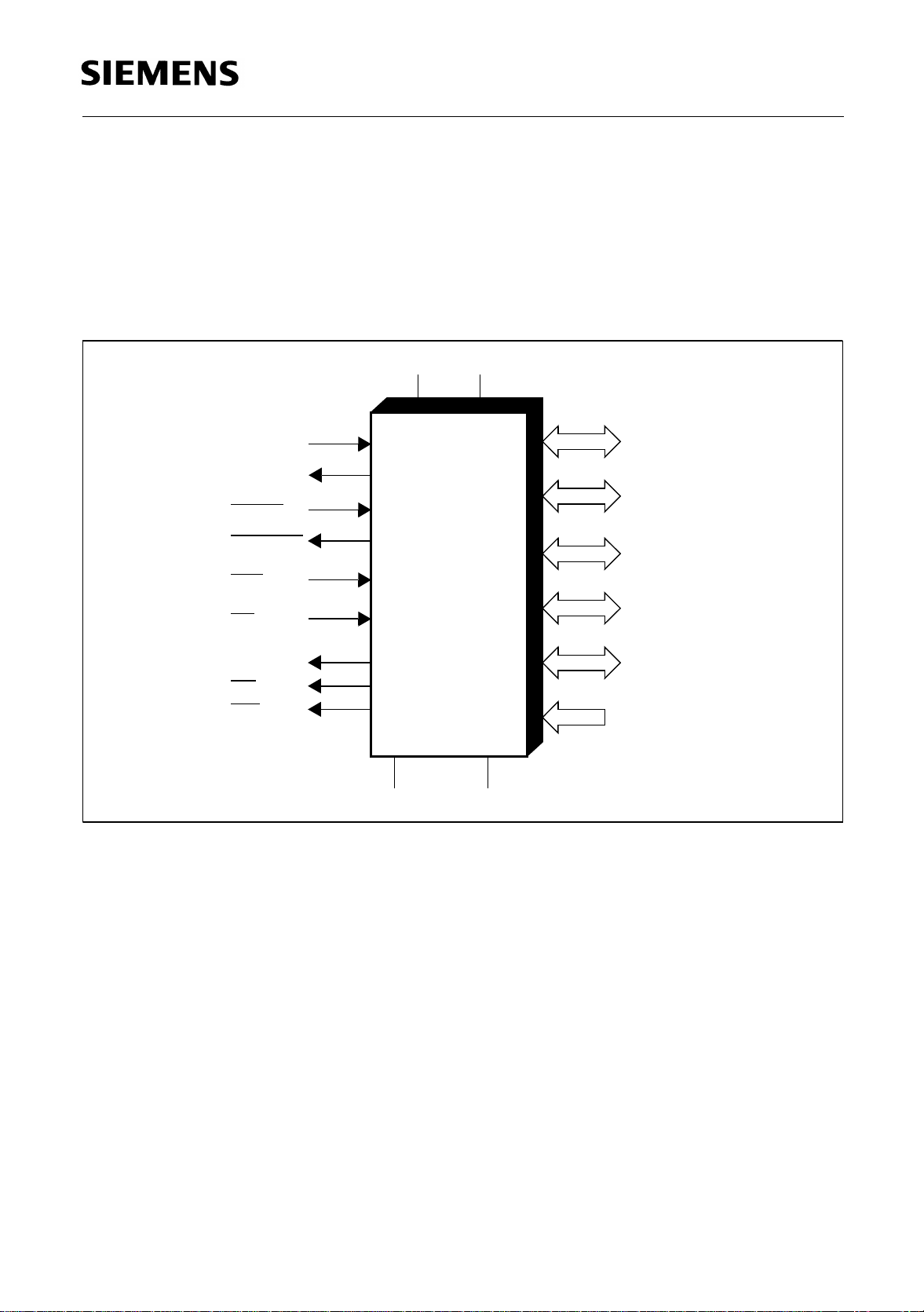
XTAL1
XTAL2
RSTIN
RSTOUT
NMI
EA
ALE
RD
WR
V
DD
C164CI
V
AREF
V
SS
V
PORT0
16 bit
PORT1
16 bit
Port 3
9 bit
Port 4
6 bit
Port 8
4 bit
Port 5
8 bit
AGND
Figure 1
Logic Symbol
Ordering Information
The ordering code for Siemens microcontrollers provides an exact reference to the required
product. This ordering code identifies:
● the derivative itself, ie. its function set
● the specified temperature range
● the package
● the type of delivery.
For the available ordering codes for the C164CI please refer to the
„Product Information Microcontrollers“, which summarizes all available microcontroller variants.
Note: The ordering codes for the Mask-ROM versions are defined for each product after
verification of the respective ROM code.
Semiconductor Group 4 1998-02
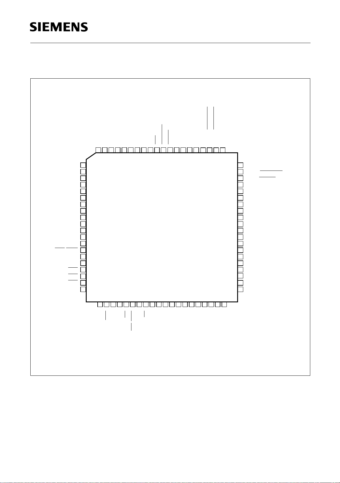
Pin Configuration
(top view)
C164CI
/EX2IN
/EX1IN
V
P5.4/AN4/T2EUD
P5.5/AN5/T4EUD
P5.6/AN6/T2IN
P5.7/AN7/T4IN
P3.12/BHE
P3.15/CLKOUT
P4.0/A16/CS3
P4.1/A17/CS2
P4.2/A18/CS1
AREF
V
SS
V
P3.4/T3EUD
P3.8/MRST
P3.9/MTSR
P3.10/TxD0
P3.11/RxD0
P3.13/SCLK
DD
P3.6/T3IN
/WRH
V
SS
AGND
V
P5.3/AN3
P5.2/AN2
P5.1/AN1
P5.0/AN0
P8.3/CC19IO
P8.2/CC18IO
P8.1/CC17IO
P8.0/CC16IO
NMI
RSTOUT
RSTIN
P1H.7/CC27IO
P1H.6/CC26IO
P1H.5/CC25IO
80797877767574737271706968676665646362
1
2
3
4
5
6
7
8
9
10
11
12
13
14
15
16
17
18
19
20
21222324252627282930313233343536373839
C164CI
DD
P1H.1/CC6POS1
P1H.4/CC24IO
P1H.3/EX3IN/T7IN
V
P1H.2/CC6POS2
61
60
59
58
57
56
55
54
53
52
51
50
49
48
47
46
45
44
43
42
41
40
V
SS
P1H.0/CC6POS0/EX0IN
P1L.7/CTRAP
P1L.6/COUT63
V
SS
XTAL1
XTAL2
V
DD
P1L.5/COUT62
P1L.4/CC62
P1L.3/COUT61
P1L.2/CC61
P1L.1/COUT60
P1L.0/CC60
P0H.7/AD15
P0H.6/AD14
P0H.5/AD13
P0H.4/AD12
P0H.3/AD11
V
ss
V
DD
RD
ALE
VPP/EA
WR/WRL
P4.3/A19/CS0
P4.6/A21/CAN_TxD
P4.5/A20/CAN_RxD
P0L.0/AD0
P0L.1/AD1
P0L.2/AD2
P0L.3/AD3
P0L.4/AD4
P0L.5/AD5
P0L.6/AD6
P0L.7/AD7
P0H.0/AD8
DD
V
P0H.1/AD9
P0H.2/AD10
Figure 2
Semiconductor Group 5 1998-02
Pin Definitions and Functions
C164CI
Symbol Pin
Number
P5.0 –
P5.7
P3.4,
P3.6,
P3.8 –
P3.13,
P3.15
76 - 79,
2 - 5
8,
9,
10 –
15,
16
8
9
10
11
12
13
14
15
16
Input (I)
Output (O)
I
I
I
I/O
I/O
I/O
I/O
I/O
I
I
I/O
I/O
O
I/O
O
I/O
O
Function
Port 5 is a 8-bit input-only port with Schmitt-Trigger
characteristics. The pins of Port 5 also serve as the (up to 8)
analog input channels for the A/D converter, where P5.x
equals ANx (Analog input channel x).
The following pins of Port 5 also serve as timer inputs:
P5.4 T2EUD GPT1 Timer T2 Ext.Up/Down Ctrl.Input
P5.5 T4EUD GPT1 Timer T4 Ext.Up/Down Ctrl.Input
P5.6 T2IN GPT1 Timer T2 Input for
Count/Gate/Reload/Capture
P5.7 T4IN GPT1 Timer T4 Input for
Count/Gate/Reload/Capture
Port 3 is a 9-bit bidirectional I/O port. It is bit-wise
programmable for input or output via direction bits. For a pin
configured as input, the output driver is put into highimpedance state.
The following Port 3 pins also serve for alternate functions:
P3.4 T3EUD GPT1 Timer T3 Ext.Up/Down Ctrl.Input
P3.6 T3IN GPT1 Timer T3 Count/Gate Input
P3.8 MRST SSC Master-Rec./Slave-Transmit I/O
P3.9 MTSR SSC Master-Transmit/Slave-Rec. O/I
P3.10 TXD0 ASC0 Clock/Data Output (Asyn./Syn.)
P3.11 RXD0 ASC0 Data Input (Asyn.) or I/O (Syn.)
P3.12 BHE
WRH
P3.13 SCLK SSC Master Clock Outp./Slave Cl. Inp.
P3.15 CLKOUT System Clock Output (=CPU Clock)
Ext. Memory High Byte Enable Signal,
Ext. Memory High Byte Write Strobe
P4.0 –
P4.3
P4.5 –
P4.6
Semiconductor Group 6 1998-02
17 - 19,
22,
23 24
17
...
22
23
24
I/O
I/O
I/O
I/O
O
O
...
O
O
O
I
O
O
Port 4 is a 6-bit bidirectional I/O port. It is bit-wise
programmable for input or output via direction bits. For a pin
configured as input, the output driver is put into highimpedance state.
In case of an external bus configuration, Port 4 can be used to
output the segment address lines:
P4.0 A16 Least Significant Segment Addr. Line
CS3
... ... ...
P4.3 A19 Segment Address Line
CS0
P4.5 A20 Segment Address Line,
CAN_RxD CAN Receive Data Input
P4.6 A21 Most Significant Segment Addr. Line,
CAN_TxD CAN Transmit Data Output
Chip Select 3 Output
Chip Select 0 Output

Pin Definitions and Functions (cont’d)
C164CI
Symbol Pin
Number
RD 25 O External Memory Read Strobe. RD is activated for every
WR
/
WRL
ALE 27 O Address Latch Enable Output. Can be used for latching the
EA
PORT0:
P0L.0 –
P0L.7,
P0H.0 P0H.7
26 O External Memory Write Strobe. In WR-mode this pin is
28 I External Access Enable pin. A low level at this pin during and
29 36
37 - 39,
42 - 46
Input (I)
Output (O)
I/O PORT0 consists of the two 8-bit bidirectional I/O ports P0L
Function
external instruction or data read access.
activated for every external data write access. In WRL
this pin is activated for low byte data write accesses on a 16bit bus, and for every data write access on an 8-bit bus. See
WRCFG in register SYSCON for mode selection.
address into external memory or an address latch in the
multiplexed bus modes.
after Reset forces the C164CI to begin instruction execution
out of external memory. A high level forces execution out of
the internal ROM.
Note: This pin also accepts the programming voltage for OTP
versions of the C164CI.
and P0H. It is bit-wise programmable for input or output via
direction bits. For a pin configured as input, the output driver
is put into high-impedance state.
In case of an external bus configuration, PORT0 serves as
the address and data (AD) bus.
Data Path Width: 8-bit 16-bit
P0L.0 – P0L.7: AD0 – AD7 AD0 - AD7
P0H.0 – P0H.7: A8 - A15 AD8 - AD15
-mode
Semiconductor Group 7 1998-02
Pin Definitions and Functions (cont’d)
C164CI
Symbol Pin
Number
PORT1:
P1L.0 –
P1L.7,
P1H.0 P1H.7
47 - 52,
57 - 58
59,
62 - 68
47
48
49
50
51
52
57
58
59
62
63
64
65
...
68
Input (I)
Output (O)
I/O
I/O
O
I/O
O
I/O
O
O
I
I
I
I
I
I
I
I
I
I
...
I
Function
PORT1 consists of the two 8-bit bidirectional I/O ports P1L and
P1H. It is bit-wise programmable for input or output via
direction bits. For a pin configured as in put, the ou tput driv er is
put into high-impedance state.
The following Port 1 pins also serve for alternate functions:
P1L.0 CC60 CAPCOM6: Input / Output of Ch. 0
P1L.1 COUT60 CAPCOM6: Output of Channel 0
P1L.2 CC61 CAPCOM6: Input / Output of Ch. 1
P1L.3 COUT61 CAPCOM6: Output of Channel 1
P1L.4 CC62 CAPCOM6: Input / Output of Ch. 2
P1L.5 COUT62 CAPCOM6: Output of Channel 2
P1L.6 COUT63 Output of 10-bit Compare Channel
P1L.7 CTRAP
CTRAP
is an input pin with an internal pullup resistor. A low
CAPCOM6: Trap Input
level on this pin switches the compare outputs of the
CAPCOM6 unit to the logic level defined by software.
P1H.0 CC6POS0
CAPCOM6: Position 0 Input
EX0IN Fast External Interrupt 0 Input
P1H.1 CC6POS1
CAPCOM6: Position 1 Input
EX1IN Fast External Interrupt 1 Input
P1H.2 CC6POS2
CAPCOM6: Position 2 Input
EX2IN Fast External Interrupt 2 Input
P1H.3 EX3IN Fast External Interrupt 3 Input
T7IN CAPCOM2: Timer T7 Count Input
P1H.4 CC24IO CAPCOM2: CC24 Capture Input
... ... ...
P1H.7 CC27IO CAPCOM2: CC27 Capture Input
XTAL1
55
I
XTAL1: Input to the oscillator amplifier and input to the
internal clock generator
XTAL2
54
O
XTAL2: Output of the oscillator amplifier circuit.
To clock the device from an external source, drive XTAL1,
while leaving XTAL2 unconnected. Minimum and maximum
high/low and rise/fall times specified in the AC Characteristics
must be observed.
RSTIN
69 I Reset Input with Schmitt-Trigger characteristics. A low level at
this pin for a specified duration while the oscillator is running
resets the C164CI. An internal pullup resistor permits power-
V
on reset using only a capacitor connected to
SS
.
In bidirectional reset mode (enabled by setting bit BDRSTEN
in register SYSCON) the RSTIN
line is pulled low for the
duration of the internal reset sequence upon a software or
WDT reset.
1)
Semiconductor Group 8 1998-02
Pin Definitions and Functions (cont’d)
C164CI
Symbol Pin
Number
RSTOUT
NMI
P8.0 –
P8.3
70 O Internal Reset Indication Output. This pin is set to a low level
71 I Non-Maskable Interrupt Input. A high to low transition at this
72 75
72
...
75
Input (I)
Output (O)
I/O
I/O
I/O
...
I/O
Function
when the part is executing either a hardware-, a software- or a
watchdog timer reset. RSTOUT
remains low until the EINIT
(end of initialization) instruction is executed.
pin causes the CPU to vector to the NMI trap routine. When
the PWRDN (power down) instruction is executed, the NMI
pin
must be low in order to force the C164CI to go into power
down mode. If NMI
is high, when PWRDN is executed, the
part will continue to run in normal mode.
If not used, pin NMI
should be pulled high externally.
Port 8 is a 4-bit bidirectional I/O port. It is bit-wise
programmable for input or output via direction bits. For a pin
configured as input, the output driver is put into highimpedance state.
The following Port 8 pins also serve for alternate functions:
P8.0 CC16IO CAPCOM2: CC16 Cap.-In/Comp.Out
... ... ...
P8.3 CC19IO CAPCOM2: CC19 Cap.-In/Comp.Out
V
AREF
V
AGND
V
DD
V
SS
1 - Reference voltage for the A/D converter.
80 - Reference ground for the A/D converter.
7, 21,
40, 53,
61
6, 20,
- Digital Supply Voltage:
+ 3 V / + 5 V during normal operation and idle mode.
≥ 2.5 V during power down mode
- Digital Ground.
41, 56,
60
1)
The following behaviour differences must be observed when the bidirectional reset is active:
● Bit BDRSTEN in register SYSCON cannot be changed after EINIT.
● After a reset bit BDRSTEN is cleared.
● Bit WDTR will always be ’0’, even after a watchdog timer reset.
● The PORT0 configuration is treated like on a hardware reset. Especially the bootstrap loader
may be activated when P0L.4 is low.
● Pin RSTIN may only be connected to external reset devices with an open drain output driver.
Semiconductor Group 9 1998-02
C164CI
Functional Description
The C164CI is a low cost downgrade of the high performance microcontroller C167CR with OTP or
internal ROM, reduced peripheral functionality and a hig h performan ce Capture Compare Unit with
an additional functionality.
The architecture of the C164CI combines advantages of both RISC and CISC processors and of
advanced peripheral subsystems in a very well-balance d way. The following block diagram gives an
overview of the different on-chip components and of the advanced, high bandwidth internal bus
structure of the C164CI.
Note: All time specifications refer to a CPU clock of 20 MHz
(see definition in the AC Characteristics section).
XTAL
P4.5/CAN_RxD
P4.6/CA N_ T xD
16
(C164CI-8RM)
(C164CI-8EM)
PLL-Oscillator
Full-CAN
Interface
V2.0B
active
5
64K
Internal ROM
or OTP
32
Instr./Data
C166-Core
CPU Core
CPU
Data
Data
16
progr. Multiplier:
0.5; 1; 1.5; 2;
2.5; 3; 4; 5
External Instr./Data
16
Interrupt Controller
PEC
up to 12
ext. IR
Interrupt Bus
Peripheral Dat a
External
Bus
(8/16 bit;
(16-bit NON MUX Data / Addresses)
MUX only)
Port 0
XBUS
&
XBUS
Control
Port 4 Port 1
Channel
Port 5
8-
10-Bit
ADC
8
USART
ASC
BRG
Sync.
Channel
(SPI)
SSC
BRG
9
GPT 1
T 2
T 3
T 4
General Purpose
Capture/Compare
Unit
Timer 7
8-Channel 16-bit
Capture/Compare Unit
(CAPCOM2)
Port 8Port 3
4
Capture/Compare Unit for
PWM Generation (CAPCOM6)
1 Compare
Channel
Timer 13
Timer 8
16
16
RTC
3/6 Capture/Compare
Channels
16
Internal
2 KByte
Dual Port
RAM
WDT
16
C164CI V1.2
Figure 3
Block Diagram
Semiconductor Group 10 1998-02

C164CI
Memory Organization
The memory space of the C164CI is configured in a Von Neumann architecture which means that
code memory, data memory, registers and I/O ports are organized within the same linear address
space which includes 4 MBytes. The entire memory space can be accessed bytewise or wordwise.
Particular portions of the on-chip memory have additionally been made directly bitaddressable.
The C164CI incorporates 64 KByte of on-chip ROM or OTP memory for code or con stant data. The
OTP memory can be programmed by the CPU itself (in system , eg. during booting) or directly via a n
external interface (eg. before assembly). The programming time is approx. 100 µsec per word. An
external programming voltage V
2 KBytes of on-chip Internal RAM are provided as a storage for user defined variables, for the
system stack, general purpose register ba nks and ev en for c ode. A reg ister b ank c an c onsis t of u p
to 16 wordwide (R0 to R15) and/or bytewide (RL0, RH0, …, RL7, RH7) so-called Gene ral Purpos e
Registers (GPRs).
1024 bytes (2 * 512 bytes) of the address space are reserved for the Special Function Register
areas (SFR space and ESFR space). SFRs are wordwide registers which are used for controlling
and monitoring functions of the different on-chip units. Unused SFR addresses are reserved for
future members of the C16x family.
= 11.5 V must be supplied for this purpose (via pin EA).
PP
In order to meet the needs of designs where more memory is required than is provi ded on c hip, u p
to 4 MBytes of external RAM and/or ROM can be connected to the microcontroller.
External Bus Controller
All of the external memory accesses are performed by a particular on-chip External Bus Controller
(EBC). It can be programmed either to Single Chip Mode when no external memory is required, or
to one of two different external memory access modes, which are as follows:
– 16-/18-/20-/22-bit Addresses, 16-bit Data, Multiplexed
– 16-/18-/20-/22-bit Addresses, 8-bit Data, Multiplexed
Important timing characteristics of the external bus interface (Memory Cycle Time, Memory Tri-
State Time, Length of ALE and Read Write Delay) have been m ade programmable to allow the user
the adaption of a wide range of different types of memories and external peripherals.
In addition, up to 4 independent address windows may be defined (via register pairs ADDRSELx /
BUSCONx) which allow to access different resources with different bus characteristics. These
address windows are arranged hierarchically where BUSCON4 overrides BUSCON3 and
BUSCON2 overrides BUSCON1. All accesses to location s not covered by these 4 address wind ows
are controlled by BUSCON0.
For applications which require less than 4 MBytes of external memory space, this address space
can be restricted to 1 MByte, 256 KByte or to 64 KByte. In this case Port 4 outputs four, two or no
address lines at all. It outputs all 6 address lines, if an address space of 4 MBytes is used.
Note: When the on-chip CAN Module is to be used the segment address output on Port 4 must be
limited to 4 bits (ie. A19...A16) in order to enable the alternate function of the CAN interface
pins.
Semiconductor Group 11 1998-02
C164CI
Central Processing Unit (CPU)
The main core of the CPU consists of a 4-stage instruction pi peline, a 16-bit arithmetic and logic unit
(ALU) and dedicated SFRs. Additional hardware has been spent for a separate mu ltipl y and d ivide
unit, a bit-mask generator and a barrel shifter.
Based on these hardware provisions, most of the C164CI’s instructions can be exec uted in just one
machine cycle which requires 100 ns at 20-MHz CPU clock. For example, shift and rotate
instructions are always processed during one machine cycle independent of the number of bits to
be shifted. All multiple-cycl e instructions have been optimized s o that they can be executed very fast
as well: branches in 2 cycles, a 16 × 16 bit multiplication in 5 cycles and a 32-/16 bit division in
10 cycles. Another pipeline optimization, the so-called ‘Jump Cach e’, allows reducing the exe cution
time of repeatedly performed jumps in a loop from 2 cycles to 1 cycle.
ROM
32
CPU
SP
STKOV
STKUN
Exec. Unit
Instr. Ptr.
Instr. Reg.
4-Stage
Pipeline
PSW
SYSCON
BUSCON 0
BUSCON 1
BUSCON 2
BUSCON 3
BUSCON 4 ADDRSEL 4
Data Page Ptr. Code Seg. Ptr.
MDH
MDL
Mul/Div-HW
Bit-Mask Gen
ALU
(16-bit)
Barrel - Shifter
Context Ptr.
ADDRSEL 1
ADDRSEL 2
ADDRSEL 3
R15
General
Purpose
Registers
R0
16
Internal
RAM
R15
R0
16
MCB02147
Figure 4
CPU Block Diagram
Semiconductor Group 12 1998-02

C164CI
The CPU disposes of an actual register context consisting of up to 16 wordwide GPRs which are
physically allocated within the on-chip RAM area. A Context Pointer (CP) register determines the
base address of the active register bank to be accessed by the CPU at a time. The number of
register banks is only restricted by the available internal RAM space. For easy parameter passing,
a register bank may overlap others.
A system stack of up to 2048 bytes is provided as a storage for temporary data. The system stack
is allocated in the on-chip RAM area, and it is accessed by the CPU via the stack pointer (SP)
register. Two separate SFRs, STKOV and STKUN, are implicitly compared against the stack
pointer value upon each stack access for the detection of a stack overflow or underflow.
The high performance offered by the hardware implem entation of the CPU can efficiently be utilized
by a programmer via the highly efficient C164CI instruction set which includes the following
instruction classes:
– Arithmetic Instructions
– Logical Instructions
– Boolean Bit Manipulation Instructions
– Compare and Loop Control Instructions
– Shift and Rotate Instructions
– Prioritize Instruction
– Data Movement Instructions
– System Stack Instructions
– Jump and Call Instructions
– Return Instructions
– System Control Instructions
– Miscellaneous Instructions
The basic instruction length is either 2 or 4 bytes. Possible op erand types are bits, by tes and words.
A variety of direct, indirect or immediate addressing modes are provided to specify the required
operands.
Semiconductor Group 13 1998-02

C164CI
Interrupt System
With an interrupt response time within a range from just 250 ns to 600 ns (in case of internal
program execution), the C164CI is capable of reacting very fast to the occurrence of nondeterministic events.
The architecture of the C164CI supports several mechanisms for fast and flexible response to
service requests that can be generated from various sources internal or external to the
microcontroller. Any of these interrupt requests can be programmed to being serviced by the
Interrupt Controller or by the Peripheral Event Controller (PEC).
In contrast to a standard interrupt service where the current program execution is suspended and
a branch to the interrupt vector table is performed, just one cycle is ‘stolen’ from the current CPU
activity to perform a PEC service. A PEC service implies a single byte or word dat a transfer between
any two memory locations with an additional increment of either the PEC source or the destination
pointer. An individual PEC transfer counter is implicity decremented for each PEC service except
when performing in the continuous transfer mode. When this counter reaches zero, a standard
interrupt is performed to the corresponding source related vector location. PEC services are very
well suited, for example, for supporting the transmi ssion or reception of b locks of data. The C164CI
has 8 PEC channels each of which offers such fast interrupt-driven data transfer capabilities.
A separate control register which contains an interrupt request fla g, an interrupt enable flag and an
interrupt priority bitfield exists for each of the possible interrupt sources. Via its related regis ter, each
source can be programmed to one of sixteen interrupt priority levels. Once having been accepted
by the CPU, an interrupt service can only be interrupted by a higher prioritize d service reques t. For
the standard interrupt processing, each of the possible interrupt sources has a dedicated vector
location.
Fast external interrupt inputs are provided to service external interrupts with high precision
requirements. These fast interrupt inputs feature program mable ed ge detecti on (rising edge, fa lling
edge or both edges).
Software interrupts are supported by means of the ‘TRAP’ instruction in combination with an
individual trap (interrupt) number.
The following table shows all of the possible C164CI interrupt sources and the corresponding
hardware-related interrupt flags, vectors, vector locations and trap (interrupt) numbers:
Source of Interrupt or PEC
Service Request
Fast External Interrupt 0 CC8IR CC8IE CC8INT 00’0060
Fast External Interrupt 1 CC9IR CC9IE CC9INT 00’0064
Fast External Interrupt 2 CC10IE CC10IE CC10INT 00’0068
Fast External Interrupt 3 CC11IE CC11IE CC11INT 00’006C
GPT1 Timer 2 T2IR T2IE T2INT 00’0088
GPT1 Timer 3 T3IR T3IE T3INT 00’008C
Request
Flag
Enable
Flag
Interrupt
Vector
Vector
Location
H
H
H
H
H
H
Trap
Number
18
H
19
H
1A
H
1B
H
22
H
23
H
Semiconductor Group 14 1998-02

C164CI
Source of Interrupt or PEC
Service Request
GPT1 Timer 4 T4IR T4IE T4INT 00’0090
Request
Flag
Enable
Flag
Interrupt
Vector
Vector
Location
H
Trap
Number
24
A/D Conversion Complete ADCIR ADCIE ADCINT 00’00A0 28
A/D Overrun Error ADEIR A DEIE ADEINT 00’00A4 29
ASC0 Transmit S0TIR S0TIE S0TINT 00’00A8
ASC0 Receive S0RIR S0RIE S0RINT 00’00AC
ASC0 Error S0EIR S0EIE S0EINT 00’00B0
SSC Transmit SCTIR SCTIE SCTINT 00’00B4
SSC Receive SCRIR SCRIE SCRINT 00’00B8
SSC Error SCEIR S CEIE SCEINT 00’00BC
CAPCOM Register 16 CC16IR CC16IE CC16INT 00’00C0
CAPCOM Register 17 CC17IR CC17IE CC17INT 00’00C4
CAPCOM Register 18 CC18IR CC18IE CC18INT 00’00C8
CAPCOM Register 19 CC19IR CC19IE CC19INT 00’00CC
CAPCOM Register 24 CC24IR CC24IE CC24INT 00’00E0
CAPCOM Register 25 CC25IR CC25IE CC25INT 00’00E4
CAPCOM Register 26 CC26IR CC26IE CC426NT 00’00E8
CAPCOM Register 27 CC27IR CC27IE CC27INT 00’00EC
CAPCOM Timer 7 T7IR T7IE T7INT 00’00F4
CAPCOM Timer 8 T8IR T8IE T8INT 00’00F8
CAPCOM 6 Interrupt CC6IR CC6IE CC6INT 00’00FC
XPER Node 0 Int / CAN XP0IR XP0IE XP0INT 00’0100
XPER Node 3 Int / PLL / T14 XP3IR XP3IE XP3INT 00’010C
ASC0 Transmit Buffer S0TBIR S0TBIE S0TBINT 00’011C
CAPCOM 6 Timer 12 T12IR T12IE T12INT 00’0134
CAPCOM 6 Timer 13 T13IR T13IE T13INT 00’0138
CAPCOM 6 Emergency CC6EIR CC6EIE CC6EINT 00’013C
2A
H
2B
H
2C
H
2D
H
2E
H
2F
H
30
H
31
H
32
H
33
H
38
H
39
H
3A
H
3B
H
3D
H
3E
H
3F
H
40
H
43
H
47
H
4D
H
4E
H
4F
H
H
H
H
H
H
H
H
H
H
H
H
H
H
H
H
H
H
H
H
H
H
H
H
H
H
H
Semiconductor Group 15 1998-02
C164CI
The C164CI also provides an excellent mechanism to identify and to process exceptions or error
conditions that arise during run-time, so-cal led ‘Hardware Trap s’. Ha rdware traps c ause im mediate
non-maskable system reaction which is similar to a standard interrupt service (branching to a
dedicated vector table location). The occurence of a hardware trap is additionally signified by an
individual bit in the trap flag register (TFR). Except when another higher prioritize d trap service is in
progress, a hardware trap will interrupt any actual program execution. In turn, hardware trap
services can normally not be interrupted by standard or PEC interrupts.
The following table shows all of the possible exceptions or error condit ions that can arise during runtime:
Exception Condition Trap
Flag
Trap
Vector
Vector
Location
Reset Functions:
Hardware Reset
Software Reset
Watchdog Timer Overflow
RESET
RESET
RESET
00’0000
00’0000
00’0000
Class A Hardware Traps:
Non-Maskable Interrupt
Stack Overflow
Stack Underflow
NMI
STKOF
STKUF
NMITRAP
STOTRAP
STUTRAP
00’0008
00’0010
00’0018
Class B Hardware Traps:
Undefined Opcode
Protected Instruction
UNDOPC
PRTFLT
BTRAP
BTRAP
00’0028
00’0028
Fault
Illegal Word Operand
ILLOPA
BTRAP
00’0028
Access
Illegal Instruction Access
Illegal External Bus
ILLINA
ILLBUS
BTRAP
BTRAP
00’0028
00’0028
Access
Reserved [2C
Software Traps
TRAP Instruction
Any
[00’0000
00’01FC
in steps
of 4
Trap
Number
00
H
H
H
H
H
H
H
H
H
H
H
– 3CH][0BH – 0FH]
H
00
00
02
04
06
0A
0A
0A
0A
0A
H
H
H
H
H
H
H
H
H
H
H
Any
–
H
]
H
H
[00
– 7FH]
H
Trap
Priority
III
III
III
II
II
II
I
I
I
I
I
Current
CPU
Priority
Semiconductor Group 16 1998-02

C164CI
The Capture/Compare Unit CAPCOM2
The general purpose CAPCOM2 unit supports generatio n and control of timing sequences on up to
8 channels with a maximum resolution of 400 ns (at 20 MHz system clock). The CAPCOM units are
typically used to handle high speed I/O tasks such as pulse and waveform generation, pulse width
modulation (PMW), Digital to Analog (D/A) conversion, software timing, or time recording relative to
external events.
Two 16-bit timers (T7/T8) with reload registers provi de two independent time bases for the captu re/
compare register array.
Each dual purpose capture/compare register, which may be individually allocated to either
CAPCOM timer and programmed for capture or compare function, has one port pin associated with
it which serves as an input pin for triggering the capture functi on, or as an output pin to ind icate the
occurence of a compare event.
When a capture/compare register has been selected for capture mode, the current contents of the
allocated timer will be latched (‘capture’d) into the capture/compare register in response to an
external event at the port pin which is associated with this register. In addition, a specific interrupt
request for this capture/compare register is generated. Either a positive, a negative, or both a
positive and a negative external signal trans ition at the pin ca n be sel ected as the triggeri ng even t.
The contents of all registers which have been selected for one of the five compare modes are
continuously compared with the contents of the allocated timers. When a match occurs between the
timer value and the value in a captu re/comp are register, specifi c actions will be tak en based on th e
selected compare mode.
Compare Modes Function
Mode 0 Interrupt-only compare mode;
several compare interrupts per timer period are possible
Mode 1 Pin toggles on each compare match;
several compare events per timer period are possible
Mode 2 Interrupt-only compare mode;
only one compare interrupt per timer period is generated
Mode 3 Pin set ‘1’ on match; pin reset ‘0’ on compare time overflow;
only one compare event per timer period is generated
Double
Register Mode
Two registers operate on one pin; pin toggles on each compare match;
several compare events per timer period are possible.
Registers CC16 & CC24 ➞ pin CC16IO
Registers CC17 & CC25 ➞ pin CC17IO
Registers CC18 & CC26 ➞ pin CC18IO
Registers CC19 & CC27 ➞ pin CC19IO
Semiconductor Group 17 1998-02

C164CI
The Capture/Compare Unit CAPCOM6
The CAPCOM6 unit supports generation and control of timing sequences on up to three 16-bit
capture/compare channels plus one 10-bit compare channel.
In compare mode the CAPCOM6 unit provides two output signals per channel wh ich have inverted
polarity and non-overlapping pulse transitions. The compare channel can generate a single PWM
output signal and is further used to modulate the capture/compare output signals.
In capture mode the contents of compare timer 12 is stored in the capture registers upon a signal
transition at pins CCx.
For motor control applications both subunits may generate versatile multichannel PWM signals
which are basically either controlled by compare timer 12 or by a typical hall sensor pattern at the
interrupt inputs (block commutation).
Compare timers 12 (16-bit) and 13 (10-bit) are free running timers which are clocked by the
prescaled CPU clock.
f
CPU
f
CPU
Period Register
T12P
Offset Register
T12OF
Prescaler
Compare Timer T12
16-Bit
1)
Mode Select Register
CC6MSEL
CC Channel 0
CC60
CC Channel 1
Control
CC61
CC Channel 2
CC62
Trap Register
Port Control Logic
CTRAP
CC60
COUT60
CC61
COUT61
CC62
COUT62
Control Register
CTCON
Compare Timer T13
1)
10-Bit
Prescaler
Period Register
T13P
1)
These Registers are not direct accessable. The period and offset registers are loading
a value into the timer registers.
Compare Register
CMP13
Block
Commutation
Control
CC6M CON.H
COUT63
CC6POS0
CC6POS1
CC6POS2
MCB03700
Figure 5
CAPCOM6 Block Diagram
Semiconductor Group 18 1998-02

C164CI
General Purpose Timer (GPT) Unit
The GPT unit represents a very flexible multifunctional timer/counter structure which may be used
for many different time related tasks such as event timing and counting, pulse width and duty cycle
measurements, pulse generation, or pulse multiplication.
The GPT unit incorporates three 16-bit timers. Each timer may operate independently in a number
of different modes, or may be concatenated with another timer.
Timer T3 can be configured for one of four basic modes of operatio n, which are Timer, Gated Tim er,
Counter, and Incremental Interface Mode. Timers T2 and T4 can only be operated in timer mode.
In Timer Mode, the input clock for a timer i s derived from the CPU clock, divided by a programmabl e
prescaler, while Counter Mode allows a timer to be clocked in reference to external events.
Pulse width or duty cycle measurement is supported in Gated Timer Mode, where the operation of
a timer is controlled by the ‘gate’ level on an external input pin. For these purposes the associated
port pin (T3IN) serves as gate or clock input. The maximum resolution of the timers is 400 ns (@
20 MHz CPU clock).
The count direction (up/down) for each timer is programmable by software or may additionally be
altered dynamically by an external signal on pin T3EUD for T3 to facilitate eg. position tracking.
In Incremental Interface Mode time r T3 can be directly co nnected to the incremental position sensor
signals A and B via the respective inputs T3IN and T3EUD. Direction and count signals are
internally derived from these two input signals, so the contents of timer T3 corresponds to the
sensor position. The third position sensor signal TOP0 can be connected to an interrupt input.
Timer T3 has an output toggle latch (T3OTL) which changes its state on each timer over-flow/
underflow. The state of this latch may be used internally to clock timers T2 and T4 for measuring
long time periods with high resolution.
In addition to their basic operating modes, timers T2 and T4 may be configured as reload registers
for timer T3. When used as reload registers, timers T2 and T4 are stopped. Timer T3 is reloaded
with the contents of T2 or T4 triggered by a selectable state transition of its toggle latch T3OTL.
Semiconductor Group 19 1998-02

C164CI
X
Figure 6
GPT Block Diagram
Watchdog Timer
The Watchdog Timer represents on e of the fail-safe mechani sms whic h have been imp lemented to
prevent the controller from malfunctioning for longer periods of time.
The Watchdog Timer is always enabled after a res et of the chip, and can only be dis abled in the time
interval until the EINIT (end of initialization) instruction has been executed. Thus, the chip’s sta rt-up
procedure is always monitored. The software has to be designed to service the Watchdog Timer
before it overflows. If, due to hardware or software related failures, the software fails to do so, the
Watchdog Timer overflows and generates an internal hardware reset and pulls the RSTOUT
in order to allow external hardware components to be reset.
The Watchdog Timer is a 16-bit timer, clocked with the system clock divided either by 2 or by 128.
The high byte of the Watchdog Timer register can be set to a prespecified reload value (stored in
WDTREL) in order to allow further variation of the monitored time interval. Each time it is serviced
by the application software, the high byte of the Watchdog Timer is reloaded. Thus, time intervals
between 25 µs and 420 ms can be monitored (@ 20 MHz). The default Watchdog Timer interval
after reset is 6.55 ms (@ 20 MHz).
pin low
Semiconductor Group 20 1998-02

C164CI
Real Time Clock
The Real Time Clock (RTC) module of the C164CI consists of a chain of 3 divider blocks, a fixed 8bit divider, the reloadable 16-bit timer T14 and the 32-bit RTC timer (accessible via registers RTCH
and RTCL). The RTC module is directly c locked with the on-chip oscillator fre quency di vided by 32
via a separate clock driver and is therefore independent from the selected clock generation mode
of the C164CI. All timers count up.
The RTC module can be used for different purposes:
● System clock to determine the current time and date
● Cyclic time based interrupt
● 48-bit timer for long term measurements
T14REL
Reload
f
T14
8:1
RTC
Interrupt
Request
RTCLRTCL
Figure 6-1
RTC Block Diagram
Note: The register associated with the RTC are not effected by a reset in order to maintain the
correct system time even when intermediate resets are executed.
Semiconductor Group 21 1998-02

C164CI
A/D Converter
For analog signal measurement, a 10-bit A/D converter with 8 multiplexed input channels and a
sample and hold circuit has been integrated on-chip. It uses the method of successive
approximation. The sample time (for loading the capacitors) and the conversion time is
programmable and can so be adjusted to the external circuitry.
Overrun error detection/protection is pro vided for the conversion result registe r (ADDAT): either a n
interrupt request will be generated when the result of a previous conv ersion has not been read from
the result register at the tim e the nex t c onvers ion is com plete, or t he next conversion is suspende d
in such a case until the previous result has been read.
For applications which require less than 8 analog input channels, the remaining channel inputs can
be used as digital input port pins.
The A/D converter of the C164CI supports four different conversion modes. In the standard Single
Channel conversion mode, the analog level on a specified channel is sampled once and converted
to a digital result. In the Single Channel Continuous mode, the analog level on a specified channel
is repeatedly sampled and converted without software intervention. In the Auto Scan mode, the
analog levels on a prespecified number of channels are sequentiall y sampled and converted. In the
Auto Scan Continuous mode, the number of prespecified channels is repeatedly sampled and
converted. In addition, the conversion of a specific cha nnel can be in serted (injected) i nto a running
sequence without disturbing this sequence. This is called Channel Injection Mode.
The Peripheral Event Controller (PEC) may be used to automatically store the conversion results
into a table in memory for later evaluation, without requiring the overhead of entering and exiting
interrupt routines for each data transfer.
After each reset and also during normal operation the ADC automatically performs calibration
cycles. This automatic self-calibration constantly adjusts the converter to changing operating
conditions (eg. temperature) and compensates process variations.
These calibration cycles ar e part of the c onversion cycle, so they do n ot affect the no rmal operation
of the A/D converter.
Semiconductor Group 22 1998-02

C164CI
Serial Channels
Serial communication with other microcontrollers, processors, terminals or external peripheral
components is provided by two serial interfaces with different functionality, an Asynchronous/
Synchronous Serial Channel (ASC0) and a High-Speed Synchronous Serial Channel (SSC).
The ASC0 is upward compatible with the serial ports of the Siemens 8-bit microcontroller families
and supports full-duplex asynchronous communication at up to 625 KBaud and half-duplex
synchronous communication at up to 2.5 MBaud @ 20 MHz CPU clock.
A dedicated baud rate generator allows to set up all standard baud rates without oscillator tuning.
For transmission, reception and error handling 4 separate interrupt vectors are provided. In
asynchronous mode, 8- or 9-bit data frames a re transmitted or received, prec eded by a start bit and
terminated by one or two stop bits. For multiprocessor communication, a mechanism to distinguish
address from data bytes has been included (8-bit data plus wake up bit mode).
In synchronous mode, the ASC0 transmits or receives bytes (8 bits) synchronously to a shift clock
which is generated by the ASC0. The ASC0 always shifts the LSB first. A loop back option is
available for testing purposes.
A number of optional hardware error detection capabilities has been included to increase the
reliability of data transfers. A parity bit can automatically be generated on transmission or be
checked on reception. Framing error detection allows to recognize data frames with missing stop
bits. An overrun error will be generated, if the last character received has not been read out of the
receive buffer register at the time the reception of a new character is complete.
The SSC supports full-duplex synchronous communication at up to 5 Mbaud @ 20 MHz CPU clock.
It may be configured so it interfaces with serially linked peripheral components. A dedicated baud
rate generator allows to set up all standard baud rates without oscillator tuning. For transmission,
reception and error handling 3 separate interrupt vectors are provided.
The SSC transmits or receives characters of 2...16 bits length synchronously to a shift clock which
can be generated by the SSC (master mode) or by an external master (slave mode). The SSC can
start shifting with the LSB or with the MSB and allows the selection of shifting and latching clock
edges as well as the clock polarity.
A number of optional hardware error detection capabilities has been included to increase the
reliability of data transfers. Transmit and receive error supervise the correct handling of the data
buffer. Phase and baudrate error detect incorrect serial data.
Semiconductor Group 23 1998-02

C164CI
CAN-Module
The integrated CAN-Module handles the completely autonomous transmission and reception of
CAN frames in accordance with the CAN specification V2.0 part B (active), ie. the on-chip CANModule can receive and transmit standard fra mes with 11-bit identi fiers as well as e xtended frames
with 29-bit identifiers.
The module provides Full CAN functionality on up to 15 message objects. Message object 15 may
be configured for Basic CAN functionality. Both modes provide separate masks for acceptance
filtering which allows to accept a number of identifiers in Full CAN mode and also allows to disregard
a number of identifiers in Basic CAN mode. All message objects can be updated independent from
the other objects and are equipped for the maximum message length of 8 bytes.
The bit timing is derived from the XCLK and is programmable up to a data rate of 1 MBaud. The
CAN-Module uses two pins of Port 4 to interface to a bus transceiver.
Note: When the CAN interface is to be used the segment address output on Port 4 must be limited
to 4 bits, ie. A19...A16. This is necessary to enable the alternate function of the CAN
interface pins.
Parallel Ports
The C164CI provides up to 59 IO lines which are organized into five input/output ports and one inp ut
port. All port lines are bit-addressable, and all input/output lines are individually (bit-wise)
programmable as inputs or outputs via direction regis ters. The I/ O ports are true bidi rectional ports
which are switched to high impedance state when c onfigured as inputs. The output driv ers of two IO
ports can be configured (pin by pin) for push/pull operation or open-drain operation via control
registers. During the internal reset, all port pins are configured as inputs.
All port lines have programmable alternate input or output functions associated with them.
PORT0 may be used as address and data lines when accessing external memory, while Port 4
outputs the additional segment address bits A21/19/17...A16 in systems where segmentation is
enabled to access more than 64 KBytes of memory.
Ports P1L, P1H and P8 are associated with the capture inputs or compare out puts of the CAPCOM
units and/or serve as external interrupt inputs.
Port 3 includes alternate functions of timers, serial interfaces, the optional bus control signal BHE
and the system clock output (CLKOUT).
Port 5 is used for the analog input channels to the A/D converter.
All port lines that are not used for these alternate functions may be used as general purpose IO
lines.
Semiconductor Group 24 1998-02
C164CI
Instruction Set Summary
The table below lists the instructions of the C164CI in a condensed way.
The various addressing modes that can be used with a specific instruction, the operation of the
instructions, parameters for conditional execution of instructions, and the opcodes for each
instruction can be found in the “C16x Family Instruction Set Manual”.
This document also provides a detailled description of each instruction.
Instruction Set Summary
Mnemonic Description Bytes
ADD(B) Add word (byte) operands 2 / 4
ADDC(B) Add word (byte) operands with Carry 2 / 4
SUB(B) Subtract word (byte) operands 2 / 4
SUBC(B) Subtract word (byte) operands with Carry 2 / 4
MUL(U) (Un)Signed multiply direct GPR by direct GPR (16-16-bit) 2
DIV(U) (Un)Signed divide register MDL by direct GPR (16-/16-bit) 2
DIVL(U) (Un)Signed long divide reg. MD by direct GPR (32-/16-bit) 2
CPL(B) Complement direct word (byte) GPR 2
NEG(B) Negate direct word (byte) GPR 2
AND(B) Bitwise AND, (word/byte operands) 2 / 4
OR(B) Bitwise OR, (word/byte operands) 2 / 4
XOR(B) Bitwise XOR, (word/byte operands) 2 / 4
BCLR Clear direct bit 2
BSET Set direct bit 2
BMOV(N) Move (negated) direct bit to direct bit 4
BAND, BOR, BXOR AND/OR/XOR direct bit with direct bit 4
BCMP Compare direct bit to direct bit 4
BFLDH/L Bitwise modify masked high/low byte of bit-addressable
direct word memory with immediate data
4
CMP(B) Compare word (byte) operands 2 / 4
CMPD1/2 Compare word data to GPR and decrement GPR by 1/2 2 / 4
CMPI1/2 Compare word data to GPR and increment GPR by 1/2 2 / 4
PRIOR Determine number of shift cycles to normalize direct
word GPR and store result in direct word GPR
SHL / SHR Shift left/right direct word GPR 2
ROL / ROR Rotate left/right direct word GPR 2
ASHR Arithmetic (sign bit) shift right direct word GPR 2
Semiconductor Group 25 1998-02
2

C164CI
Instruction Set Summary (cont’d)
Mnemonic Description Bytes
MOV(B) Move word (byte) data 2 / 4
MOVBS Move byte operand to word operand with sign extension 2 / 4
MOVBZ Move byte operand to word operand. with zero extension 2 / 4
JMPA, JMPI, JMPR Jump absolute/indirect/relative if condition is met 4
JMPS Jump absolute to a code segment 4
J(N)B Jump relative if direct bit is (not) set 4
JBC Jump relative and clear bit if direct bit is set 4
JNBS Jump relative and set bit if direct bit is not set 4
CALLA, CALLI, CALLR Call absolute/indirect/relative subroutine if condition is met 4
CALLS Call absolute subroutine in any code segment 4
PCALL Push direct word register onto system stack and call
absolute subroutine
TRAP Call interrupt service routine via immediate trap number 2
PUSH, POP Push/pop direct word register onto/from system stack 2
SCXT Push direct word register onto system stack und update
register with word operand
RET Return from intra-segment subroutine 2
RETS Return from inter-segment subroutine 2
RETP Return from intra-segment subroutine and pop direct
word register from system stack
RETI Return from interrupt service subroutine 2
SRST Software Reset 4
IDLE Enter Idle Mode 4
PWRDN Enter Power Down Mode
(supposes NMI
SRVWDT Service Watchdog Timer 4
DISWDT Disable Watchdog Timer 4
-pin being low)
4
4
2
4
EINIT Signify End-of-Initialization on RSTOUT-pin 4
ATOMIC Begin ATOMIC sequence 2
EXTR Begin EXTended Register sequence 2
EXTP(R) Begin EXTended Page (and Register) sequence 2 / 4
EXTS(R) Begin EXTended Segment (and Register) sequence 2 / 4
NOP Null operation 2
Semiconductor Group 26 1998-02

C164CI
Special Function Registers Overview
The following table lists all SFRs which are implemented in the C164CI in alphabetical order.
Bit-addressable SFRs are marked with the letter “b” in column “Na me”. SFRs within the Extended
SFR-Space (ESFRs) are marked with the letter “E” in column “Physical Address”.
An SFR can be specified via its individua l mnemonic name. Depending on the selec ted addressin g
mode, an SFR can be accessed via its physical address (using the Data Page Pointers), or via its
short 8-bit address (without using the Data Page Pointers).
Name Physical
Address
ADCIC b FF98
H
8-Bit
Address
CC
H
Description Reset
Value
A/D Converter End of Conversion Interrupt
0000
Control Register
ADCON b FFA0
ADEIC b FF9A
D0
H
H
CD
H
H
A/D Converter Control Register 0000
A/D Converter Overrun Error Interrupt Control
0000
Register
ADDAT FEA0
ADDAT2 F0A0HE 50
ADDRSEL1 FE18
ADDRSEL2 FE1A
ADDRSEL3 FE1C
ADDRSEL4 FE1E
BUSCON0 b FF0C
BUSCON1 b FF14
BUSCON2 b FF16
BUSCON3 b FF18
BUSCON4 b FF1A
50
H
H
H
H
H
H
H
H
H
H
0C
0D
0E
0F
86
8A
8B
8C
8D
H
H
H
H
H
H
H
H
H
H
H
A/D Converter Result Register 0000
A/D Converter 2 Result Register 0000
Address Select Register 1 0000
Address Select Register 2 0000
Address Select Register 3 0000
Address Select Register 4 0000
Bus Configuration Register 0 0000
Bus Configuration Register 1 0000
Bus Configuration Register 2 0000
Bus Configuration Register 3 0000
Bus Configuration Register 4 0000
C1BTR EF04HX --- CAN Bit Timing Register UUUU
C1CSR EF00HX --- CAN Control / Status Register XX01
C1GMS EF06HX --- CAN Global Mask Short UFUU
C1IR EF02HX --- CAN Interrupt Register XX
C1LGML EF0AHX --- CAN Lower Global Mask Long UUUU
C1LMLM EF0EHX --- CAN Lower Mask of Last Message UUUU
C1UGML EF08HX --- CAN Upper Global Mask Long UUUU
C1UMLM EF0CHX --- CAN Upper Mask of Last Message UUUU
CC10IC b FF8C
CC11IC b FF8E
C6
H
H
C7
H
H
CAPCOM Register 10 Interrupt Control Register 0000
CAPCOM Register 11 Interrupt Control Register 0000
H
H
H
H
H
H
H
H
H
H
H
H
H
H
H
H
H
H
H
H
H
H
H
H
Semiconductor Group 27 1998-02

C164CI
Name Physical
Address
CC16 FE60
H
8-Bit
Address
30
H
CC16IC b F160HE B0
CC17 FE62
31
H
H
CC17IC b F162HE B1
CC18 FE64
32
H
H
CC18IC b F164HE B2
CC19 FE66
33
H
H
CC19IC b F166HE B3
CC24 FE70
38
H
H
CC24IC b F170HE B8
CC25 FE72
39
H
H
CC25IC b F172HE B9
CC26 FE74
3A
H
CC26IC b F174HE BA
CC27 FE76
3B
H
CC27IC b F176HE BB
CC60 FE30
CC61 FE32
CC62 FE34
18
H
H
H
19
1A
H
H
CC6EIC b F188HE C4
CC6IC b F17EHEBF
CC6MCON b FF32
CC6MIC b FF36
99
H
H
H
9B
CC6MSEL F036HE 1B
CC8IC b FF88
CC9IC b FF8A
CCM4 b FF22
CCM6 b FF26
CMP13 FE36
CP FE10
CSP FE08
C4
H
C5
H
91
H
H
H
H
H
93
1B
08
04
H
H
H
H
Description Reset
Value
CAPCOM Register 16 0000
H
CAPCOM Register 16 Interrupt Control Register 0000
CAPCOM Register 17 0000
H
CAPCOM Register 17 Interrupt Control Register 0000
CAPCOM Register 18 0000
H
CAPCOM Register 18 Interrupt Control Register 0000
CAPCOM Register 19 0000
H
CAPCOM Register 19 Interrupt Control Register 0000
CAPCOM Register 24 0000
H
CAPCOM Register 24 Interrupt Control Register 0000
CAPCOM Register 25 0000
H
H
H
H
H
CAPCOM Register 25 Interrupt Control Register 0000
CAPCOM Register 26 0000
CAPCOM Register 26 Interrupt Control Register 0000
CAPCOM Register 27 0000
CAPCOM Register 27 Interrupt Control Register 0000
CAPCOM 6 Register 0 0000
CAPCOM 6 Register 1 0000
H
H
H
CAPCOM 6 Register 2 0000
CAPCOM 6 Emergency Interrupt Control Reg. 0000
CAPCOM 6 Interrupt Control Register 0000
CAPCOM 6 Mode Control Register 00FF
H
H
H
H
CAPCOM 6 Mode Interrupt Control Register 0000
CAPCOM 6 Mode Select Register 0000
CAPCOM Register 8 Interrupt Control Register 0000
CAPCOM Register 9 Interrupt Control Register 0000
CAPCOM Mode Control Register 4 0000
CAPCOM Mode Control Register 6 0000
H
CAPCOM 6 Timer 13 Compare Register 0000
CPU Context Pointer Register FC00
CPU Code Segment Pointer Register
0000
H
H
H
H
H
H
H
H
H
H
H
H
H
H
H
H
H
H
H
H
H
H
H
H
H
H
H
H
H
H
H
(8 bits, not directly writeable)
CTCON b FF30
98
H
H
CAPCOM 6 Compare Timer Control Register 1010
H
Semiconductor Group 28 1998-02

C164CI
Name Physical
Address
DP0H b F102HE 81
DP0L b F100HE 80
DP1H b F106HE 83
DP1L b F104HE 82
DP3 b FFC6
DP4 b FFCA
DP8 b FFD6
DPP0 FE00
DPP1 FE02
DPP2 FE04
DPP3 FE06
EXICON b F1C0HE E0
EXISEL b F1DAHE ED
IDCHIP F07CHE 3E
IDMANUF F07EHE 3F
IDMEM F07AHE 3D
IDPROG F078HE 3C
ISNC b F1DEHE EF
LAR EFn4HX --- CAN Lower Arbitration Register (msg. n)UUUU
MCFG EFn6HX --- CAN Message Configuration Register (msg. n)UU
MCR EFn0HX --- CAN Message Control Register (msg. n)UUUU
MDC b FF0E
MDH FE0C
MDL FE0E
ODP3 b F1C6HE E3
ODP8 b F1D6HE EB
ONES b FF1E
OPAD EDC2HX --- OTP Programming Interface Address Register 0000
OPCTRL EDC0HX --- OTP Programming Interface Control Register 0007
OPDAT EDC4HX --- OTP Programming Interface Data Register 0000
P0H b FF02
P0L b FF00
P1H b FF06
H
H
H
H
H
H
H
H
H
H
H
H
H
H
8-Bit
Address
H
H
H
H
E3
H
E5
H
EB
H
00
H
01
H
02
H
03
H
H
H
H
H
H
H
H
87
H
06
H
07
H
H
H
8F
H
81
H
80
H
83
H
Description Reset
Value
P0H Direction Control Register 00
P0L Direction Control Register 00
P1H Direction Control Register 00
P1L Direction Control Register 00
Port 3 Direction Control Register 0000
Port 4 Direction Control Register 00
Port 8 Direction Control Register 00
CPU Data Page Pointer 0 Register (10 bits) 0000
CPU Data Page Pointer 1 Register (10 bits) 0001
CPU Data Page Pointer 2 Register (10 bits) 0002
CPU Data Page Pointer 3 Register (10 bits) 0003
External Interrupt Control Register 0000
External Interrupt Source Select Register 0000
Identifier 0A01
Identifier 1820
Identifier X010
Identifier XXXX
Interrupt Subnode Control Register 0000
CPU Multiply Divide Control Register 0000
CPU Multiply Divide Register – High Word 0000
CPU Multiply Divide Register – Low Word 0000
Port 3 Open Drain Control Register 0000
Port 8 Open Drain Control Register 00
Constant Value 1’s Register (read only) FFFF
Port 0 High Register (Upper half of PORT0) 00
Port 0 Low Register (Lower half of PORT0) 00
Port 1 High Register (Upper half of PORT1) 00
H
H
H
H
H
H
H
H
H
H
H
H
H
H
H
H
H
H
H
H
H
H
H
H
H
H
H
H
H
H
H
H
H
Semiconductor Group 29 1998-02

C164CI
Name Physical
Address
P1L b FF04
P3 b FFC4
P4 b FFC8
P5 b FFA2
P5DIDIS b FFA4
P8 b FFD4
PECC0 FEC0
PECC1 FEC2
PECC2 FEC4
PECC3 FEC6
PECC4 FEC8
PECC5 FECA
PECC6 FECC
PECC7 FECE
H
H
H
H
H
H
H
H
H
H
H
H
H
H
8-Bit
Address
82
E2
E4
D1
D2
EA
60
61
62
63
64
65
66
67
PICON b F1C4HE E2
PSW b FF10
88
H
RP0H b F108HE 84
RTCH F0D6HE 6B
RTCL F0D4HE 6A
S0BG FEB4
5A
H
Description Reset
Value
H
H
H
H
H
H
H
H
H
H
H
H
H
H
H
H
H
H
H
H
Port 1 Low Register (Lower half of PORT1) 00
Port 3 Register 0000
Port 4 Register (8 bits) 00
Port 5 Register (read only) XXXX
Port 5 Digital Input Disable Register 0000
Port 8 Register (8 bits) 00
PEC Channel 0 Control Register 0000
PEC Channel 1 Control Register 0000
PEC Channel 2 Control Register 0000
PEC Channel 3 Control Register 0000
PEC Channel 4 Control Register 0000
PEC Channel 5 Control Register 0000
PEC Channel 6 Control Register 0000
PEC Channel 7 Control Register 0000
Port Input Threshold Control Register 0000
CPU Program Status Word 0000
System Startup Configuration Register (Rd. only) XX
RTC High Register XXXX
RTC Low Register XXXX
Serial Channel 0 Baud Rate Generator Reload
0000
H
H
H
H
H
H
H
H
H
H
H
H
H
H
H
H
H
H
H
H
Register
S0CON b FFB0
S0EIC b FF70
S0RBUF FEB2
D8
H
H
H
B8
59
H
H
H
Serial Channel 0 Control Register 0000
Serial Channel 0 Error Interrupt Control Register 0000
Serial Channel 0 Receive Buffer Register
XXXX
H
H
H
(read only)
S0RIC b FF6E
B7
H
H
Serial Channel 0 Receive Interrupt Control
0000
H
Register
S0TBIC b F19CHE CE
H
Serial Channel 0 Transmit Buffer Interrupt Control
0000
H
Register
S0TBUF FEB0
S0TIC b FF6C
58
H
H
B6
H
H
Serial Channel 0 Transmit Buffer Register 0000
Serial Channel 0 Transmit Interrupt Control
0000
H
H
Register
SP FE12
SSCBR F0B4HE 5A
09
H
H
H
CPU System Stack Pointer Register FC00
SSC Baudrate Register 0000
H
H
Semiconductor Group 30 1998-02

C164CI
Name Physical
Address
SSCCON b FFB2
SSCEIC b FF76
H
H
8-Bit
Address
D9
BB
SSCRB F0B2HE 59
SSCRIC b FF74
BA
H
SSCTB F0B0HE 58
SSCTIC b FF72
STKOV FE14
STKUN FE16
SYSCON b FF12
B9
H
0A
H
0B
H
89
H
SYSCON2 b F1D0HE E8
SYSCON3 b F1D4HE EA
T12IC b F190HE C8
T12OF F034HE 1A
T12P F030HE 18
T13IC b F198HE CC
T13P F032HE 19
T14 F0D2HE 69
T14REL F0D0HE 68
T2 FE40
T2CON b FF40
T2IC b FF60
T3 FE42
T3CON b FF42
T3IC b FF62
T4 FE44
T4CON b FF44
T4IC b FF64
20
H
A0
H
B0
H
21
H
A1
H
B1
H
22
H
A2
H
B2
H
T7 F050HE 28
T78CON b FF20
90
H
T7IC b F17AHE BD
T7REL F054HE 2A
T8 F052HE 29
T8IC b F17CHE BE
Description Reset
Value
H
H
H
H
H
H
H
H
H
H
H
H
H
H
H
H
H
H
H
H
H
H
H
H
H
H
H
H
H
H
H
H
H
SSC Control Register 0000
SSC Error Interrupt Control Register 0000
SSC Receive Buffer (read only) XXXX
SSC Receive Interrupt Control Register 0000
SSC Transmit Buffer (write only) 0000
SSC Transmit Interrupt Control Register 0000
CPU Stack Overflow Pointer Register FA00
CPU Stack Underflow Pointer Register FC00
CPU System Configuration Register 0XX0
CPU System Configuration Register 2 0000
CPU System Configuration Register 3 0000
CAPCOM 6 Timer 12 Interrupt Control Register 0000
CAPCOM 6 Timer 12 Offset Register 0000
CAPCOM 6 Timer 12 Period Register 0000
CAPCOM 6 Timer 13 Interrupt Control Register 0000
CAPCOM 6 Timer 13 Period Register 0000
RTC Timer 14 Register XXXX
RTC Timer 14 Reload Register XXXX
GPT1 Timer 2 Register 0000
GPT1 Timer 2 Control Register 0000
GPT1 Timer 2 Interrupt Control Register 0000
GPT1 Timer 3 Register 0000
GPT1 Timer 3 Control Register 0000
GPT1 Timer 3 Interrupt Control Register 0000
GPT1 Timer 4 Register 0000
GPT1 Timer 4 Control Register 0000
GPT1 Timer 4 Interrupt Control Register 0000
CAPCOM Timer 7 Register 0000
CAPCOM Timer 7 and 8 Control Register 0000
CAPCOM Timer 7 Interrupt Control Register 0000
CAPCOM Timer 7 Reload Register 0000
CAPCOM Timer 8 Register 0000
CAPCOM Timer 8 Interrupt Control Register 0000
H
H
H
H
H
H
H
H
1)
H
H
H
H
H
H
H
H
H
H
H
H
H
H
H
H
H
H
H
H
H
H
H
H
H
Semiconductor Group 31 1998-02

C164CI
Name Physical
Address
T8REL F056
TFR b FFAC
TRCON b FF34
UAR EFn2HX --- CAN Upper Arbitration Register (msg. n)UUUU
WDT FEAE
WDTCON b FFAE
XP0IC b F186HE C3
XP3IC b F19EHE CF
ZEROS b FF1C
1)
The system configuration is selected during reset.
2)
The reset value depends on the indicated reset source.
H
H
H
H
H
H
8-Bit
Address
E 2B
D6
9A
57
D7
8E
Description Reset
Value
H
H
H
H
H
H
H
H
CAPCOM Timer 8 Reload Register 0000
Trap Flag Register 0000
CAPCOM 6 Trap Enable Control Register 00XX
Watchdog Timer Register (read only) 0000
Watchdog Timer Control Register 00XX
X-Peripheral 0 Interrupt Control Register 0000
X-Peripheral 3 Interrupt Control Register 0000
Constant Value 0’s Register (read only) 0000
H
H
H
H
H
2)
H
H
H
H
Semiconductor Group 32 1998-02

Absolute Maximum Ratings
C164CI
Ambient temperature under bias (
T
):
A
SAF-C164CI ................................................................................................................–40 to +85 °C
SAK-C164CI ..............................................................................................................–40 to +125 °C
T
Storage temperature (
Voltage on
V
pins with respect to ground (
DD
Voltage on any pin with respect to ground (
)........................................................................................– 65 to +150 °C
ST
V
) ..................................................... –0.5 to +6.5 V
SS
V
).................................................–0.5 to
SS
V
+0.5 V
DD
Input current on any pin during overload condition.................................................... –10 to +10 mA
Absolute sum of all input currents during overload condition ..............................................|100 mA|
Power dissipation..................................................................................................................... 1.5 W
Note: Stresses above those listed under “Absolute Maximum Ratings” may cause permanent
damage to the device. This is a stress rating only and functional operation of the device at
these or any other conditions above those indicated in the operational sections of this
specification is not implied. Exposure to absolute maximum rating conditions for extended
periods may affect device reliability.
V
>
V
or
V
<
V
During absolute maximum rating overload conditions (
V
pins with respect to ground (
DD
V
) must not exceed the values defined by the absolute
SS
IN
DD
IN
) the voltage on
SS
maximum ratings.
Parameter Interpretation
The parameters listed in the following partly represent the characteristics of the C164CI and partly
its demands on the system. To aid in interpreting the parameters right, when evaluating them for a
design, they are marked in column “Symbol”:
CC (Controller Characteristics):
The logic of the C164CI will provide signals with the respective timing characteristics.
SR (System Requirement):
The external system must provide signals with the respective timing characteristics to the C164CI.
Semiconductor Group 33 1998-02

C164CI
DC Characteristics
V
= 4.25 - 5.5 V;
DD
T
= -40 to +85 °C for SAF-C164CI
A
T
= -40 to +125 °C for SAK-C164CI
A
Parameter Symbol Limit Values Unit Test Condition
V
= 0 V; f
SS
= 20 MHz
CPU
min. max.
Input low voltage
V
(TTL)
Input low voltage
V
(Special Threshold)
Input high voltage, all except
RSTIN
and XTAL1 (TTL)
Input high voltage RSTIN
Input high voltage XTAL1
Input high voltage
V
V
V
V
(Special Threshold)
Input Hysteresis
HYS 400 - mV –
(Special Threshold)
Output low voltage
(PORT0, PORT1, Port 4, ALE, RD
WR
, BHE, CLKOUT, RSTOUT)
Output low voltage
V
,
V
(all other outputs)
Output high voltage
(PORT0, PORT1, Port 4, ALE, RD
WR
, BHE, CLKOUT, RSTOUT)
Output high voltage
1)
V
,
V
(all other outputs)
Input leakage current (Port 5)
I
Input leakage current (all other) I
Overload current I
RSTIN pullup resistor R
Read/Write inactive current
Read/Write active current
ALE inactive current
ALE active current
4)
4)
4)
PORT0 configuration current
4)
4)
I
I
I
I
I
I
SR – 0.5 0.2
IL
V
DD
V–
– 0.1
SR – 0.5 2.0 V –
ILS
IH
SR 0.2
V
DD
V
+ 0.5 V –
DD
+ 0.9
IH1
IH2
IHS
SR 0.6
SR 0.7
SR 0.8
V
DD
V
DD
V
DD
V
+ 0.5 V –
DD
V
+ 0.5 V –
DD
V
+ 0.5 V –
DD
- 0.2
CC – 0.45 V IOL = 2.4 mA
OL
CC – 0.45 V I
OL1
OH
CC 0.9
V
DD
–V
2.4
OH1
CC 0.9
V
DD
2.4
CC – ±200 nA 0.45V<
OZ1
CC – ±500 nA 0.45V<
OZ2
SR – ±5mA
OV
CC 50 250 kΩ –
RST
2)
RWH
RWL
ALEL
ALEH
P0H
P0L
3)
–-40µA V
3)
-500 – µA V
2)
–40µA V
3)
500 – µA V
2)
–-10µA VIN = V
-100 – µA VIN = V
–V
V
OL1
I
OH
I
OH
I
OH
I
OH
5) 8)
= 1.6 mA
= – 500 µA
= – 2.4 mA
= – 250 µA
= – 1.6 mA
V
IN
V
IN
= 2.4 V
OUT
= V
OUT
OUT
OUT
OLmax
= V
OLmax
= 2.4 V
IHmin
ILmax
<
<
V
DD
V
DD
Semiconductor Group 34 1998-02
C164CI
Parameter Symbol Limit Values Unit Test Condition
min. max.
XTAL1 input current I
Pin capacitance
5)
(digital inputs/outputs)
Power supply current (active)
with all peripherals active
Idle mode supply current
with all peripherals active
Idle mode supply current
with all peripherals deactivated,
CC – ±20 µA0 V < VIN < V
IL
C
CC – 10 pF f = 1 MHz
IO
I
DD
I
IDX
I
IDO
– 10 +
3.5 ×
f
CPU
–5 +
1.25 ×
– 500 +
f
50 ×
OSC
mA RSTIN = V
mA RSTIN = V
f
CPU
µA RSTIN = V
9)
T
= 25 °C
A
f
in [MHz]
CPU
f
in [MHz]
CPU
f
in [MHz]
CPU
PLL off, SDD factor = 32
Power-down mode supply current
with RTC running
Power-down mode supply current
I
I
PDR
PDO
– 100 +
25 ×
f
OSC
µA VDD = 5.5 V
9)
f
OSC
in [MHz]
–50µA VDD = 5.5 V
with RTC disabled
Notes
1)
This specification is not valid for ou tputs which are swit ched to open drain mode. In this case th e respective
output will float and the voltage resu lt s from th e ex t ernal circuitry.
2)
The maximum current may be draw n while the respective signal line rem ains inactive.
3)
The minimum current must be drawn in order to drive the respective signal line active.
4)
This specification is only valid du ring Reset, or during Adapt-mode.
5)
Not 100% tested, guaranteed by design characterization.
6)
The supply current is a function of the operating frequency. This dependency is illustrated in the figure below.
These parameters are tested at
V
or VIH.
IL
The oscillator also contributes to the total supply current. The given values refer to the worst case, i.e.
For lower oscillator frequencies the respective supply curren t can be reduced accordingly.
7)
This parameter is tested includ ing leakage cu rrents. All inputs (including pins co nfigured as input s) at 0 V to
0.1 V or at
8)
Overload conditions under operating conditions occur if the voltage on the respective pin exceeds the specified
operating range (i.e.
on all port pins may not exceed 50 mA. Th e supply volt age (
limits.
9)
This parameter is det ermined mainly by the current consum ed by the oscillator. This current, howev er, is
influenced by the external oscilla tor circu itry (crys tal, cap acitors). T he values given refer to a typical circ uitry
and may change in case of a not opt im ize d ex t ernal oscillator circuitry.
A typical value for
V
– 0.1 V to VDD, V
DD
V
OV
I
PDR
at room temperature and f
V
> VDD+ 0.5 V o r VOV< VSS– 0.5 V). The absolute sum o f input overload curre nts
and 20 MHz CPU clock with all outputs disconnected and all inputs at
DDmax
= 0 V, all outputs (including pins configured as outputs) disconnec te d.
REF
V
and VSS) must remain within the specified
DD
= 16 MHz is 300 µA.
OSC
I
DD
IL2
6)
IH1
6)
IH1
6)
7)
7)
PDRmax
.
Semiconductor Group 35 1998-02
80
40
C164CI
I
DDmax
I [mA]
I
DDtyp
I
IDXmax
I
IDXtyp
10
5
10 15 20
Figure 7
Active and Idle Supply Current as a Function of Operating Frequency
I [µA]
1500
1250
1000
750
500
f
[MHz]
CPU
I
IDOmax
I
IDOtyp
I
PDRmax
250
I
PDOmax
f
[MHz]
4
8 12 16
OSC
Figure 8
Idle and Power Down Supply Current as a Function of Oscillator Frequency
Semiconductor Group 36 1998-02
AC Characteristics
Definition of Internal Timing
C164CI
The internal operation of the C164CI is controlled by the internal CPU clock f
. Both edges of the
CPU
CPU clock can trigger internal (eg. pipeline) or external (eg. bus cycles) operations.
The specification of the external timing (AC Characte ristics) therefore depends on the time be tween
two consecutive edges of the CPU clock, called “TCL” (see figure below).
Phase Locked Loop Operation
f
XTAL
f
CPU
TCLTCL
Direct Clock Drive
f
XTAL
f
CPU
TCLTCL
Prescaler Operation
f
XTAL
f
CPU
TCL TCL
Figure 9
Generation Mechanisms for the CPU Clock
The CPU clock signal can be generated via different mechanisms. The duration of TCLs and their
variation (and also the derived external timing) depends on the used mec hanis m to generate f
CPU
This influence must be regarded when calculating the timings for the C164CI.
Note: The example for PLL operation shown in the figure above refers to a PLL factor of 4.
The used mechanism to generate the CPU clock is selected during reset via the logic levels on pins
P0.15-13 (P0H.7-5).
The table below associates th e combinations of these three bi ts with the respective cloc k generation
mode.
.
Semiconductor Group 37 1998-02
C164CI Clock Generation Modes
C164CI
P0.15-13
(P0H.7-5)
111
110
101
100
011
010 f
001
000
1)
The external clock input range refers to a CPU clock range of 10...20 MHz.
2)
The maximum frequency depends on the duty cycle of the external clock signal.
CPU Frequency
f
CPU
f
f
f
f
f
XTAL
f
f
XTAL
= f
XTAL
XTAL
XTAL
XTAL
XTAL
XTAL
* F
XTAL
* 4 2.5 to 5 MHz Default configuration
* 3 3.33 to 6.66 MHz
* 2 5 to 10 MHz
* 5 2 to 4 MHz
* 1 1 to 20 MHz Direct drive
* 1.5 6.66 to 13.3 MHz
/ 2 2 to 40 MHz CPU clock via prescaler
* 2.5 4 to 8 MHz
External Clock Input
Range
1)
Notes
2)
Prescaler Operation
When pins P0.15-13 (P0H.7-5) equal ’001’ during reset the CPU clock is derived from the internal
oscillator (input clock signal) by a 2:1 prescaler.
The frequency of f
duration of an individual TCL) is defined by the period of the input clock f
is half the frequency of f
CPU
and the high and low time of f
XTAL
XTAL
(ie. the
CPU
.
The timings listed in the AC Characteristics that refe r to TCLs therefore can be calculated us ing the
period of f
for any TCL.
XTAL
Direct Drive
When pins P0.15-13 (P0H.7-5) equal ’011’ during reset the on-chip phase locked loop is disabled
and the CPU clock is directly driven from the internal oscillator with the input clock signal.
The frequency of f
directly follows the frequency of f
CPU
duration of an individual TCL) is defined by the duty cycle of the input clock f
so the high and low time of f
XTAL
XTAL
(ie. the
CPU
.
The timings listed below that refer to TCLs therefore must be calculated using the minimum TCL
that is possible under the respective circumstances. This minimum value can be calculated via the
following formula:
TCL
For two consecutive TCLs the deviation caused by the duty cycle of f
duration of 2TCL is always 1/f
min
= 1/f
* DC
XTAL
XTAL
min
. The minimum value TCL
(DC = duty cycle)
is compensated so the
XTAL
therefore has to be used only once
min
for timings that require an odd number of TCLs (1,3,...). Timings that require an even number of
TCLs (2,4,...) may use the formula 2TCL = 1/f
Note: The address float timings in Multiplexed bu s mode (t
TCL (TCL
max
= 1/f
XTAL
* DC
) instead of TCL
max
XTAL
.
and t45) use the maximum duration of
11
.
min
Semiconductor Group 38 1998-02

C164CI
Phase Locked Loop
For all other combinations of pin s P0.15-13 (P0H.7-5) during res et the on-chip pha se locked loo p is
enabled and provides the CPU clock (see table above). The PLL multiplies the input frequency by
the factor F which is selected via the combination of pins P0.15 -13 (ie. f
F’th transition of f
the PLL circuit synchronizes the CPU clock to the input clock. This
XTAL
synchronization is done smoothely, ie. the CPU clock frequency does not change abruptly.
CPU
= f
* F). With every
XTAL
Due to this adaptation to the input clock the frequency of f
to f
. The slight variation causes a jitter of f
XTAL
which also effects the duration of i ndividual TCLs.
CPU
is constantly adjusted so it is locked
CPU
The timings listed in the AC Characte ristics that refer to TCLs therefore mus t be calculated using the
minimum TCL that is possible under the respective circumstances.
The actual minimum value for TCL depends on the jitter of the PLL. As the PLL is constantly
adjusting its output frequency so it corresponds to the applied input frequenc y (crystal or oscill ator)
the relative deviation for periods of more than one TCL is lower than for one single TCL (see formula
and figure below).
N
For a period of
So for a period of 3 TCLs (ie.
and (3TCL)
* TCL the minimum value is computed using the corresponding deviation DN:
= 3TCL
min
TCL
= TCL
min
N
* (1 - 3.8 / 100) = 3TCL
NOM
* (1 - DN / 100) DN = ±(4 - N /15) [%],
NOM
N
where
and 1 ≤
= number of consecutive TCLs
N
≤ 40.
= 3): D3 = 4 - 3/15 = 3.8%,
* 0.962 (57.72 nsec @ f
NOM
CPU
= 25 MHz).
This is especially impo rtant for bus cycles using waitstates and eg. for the operation o f timers, serial
interfaces, etc. For all slower operations and longer periods (eg. pulse train generation or
measurement, lower baudrates, etc.) the deviation caused by the PLL jitter is neglectible.
Max.jitter [%]
±4
±3
±2
±1
42
8
Figure 10
Approximated Maximum PLL Jitter
This approximated formula is valid for
1 ≤ N ≤ 40 and 10MHz ≤ f
≤ 25MHz.
CPU
3216
N
Semiconductor Group 39 1998-02
C164CI
AC Characteristics
External Clock Drive XTAL1
V
= 4.25 - 5.5 V; VSS = 0 V
DD
T
= -40 to +85 °C for SAF-C164CI
A
T
= -40 to +125 °C for SAK-C164CI
A
Parameter Symbol Direct Drive 1:1 Prescaler 2:1 PLL 1:N Unit
min. max. min. max. min. max.
Oscillator period
High time
Low time
Rise time
Fall time
t
SR 50 8000 25 4000 75
OSC
t
SR 18
1
t
SR 18
2
t
SR – 10
3
t
SR – 10
4
2)
2)
–6–10–ns
–6–10–ns
2)
2)
–6 2)– 10
–6 2)– 10
1)
500
1)
ns
2)
2)
ns
ns
1)
The minimum and maximum oscillator periods for PLL operation depend on the selected
CPU clock generation mode. Please see respective table above.
2)
The clock input signal must reach the defined levels VIL and V
IH2
.
0.5
t
1
V
CC
t
e
t
t
3
asc
t
4
MCT02534
V
IH2
V
IL
Figure 11
External Clock Drive XTAL1
Semiconductor Group 40 1998-02

C164CI
A/D Converter Characteristics
V
= 4.25 - 5.5 V; VSS = 0 V
DD
T
= -40 to +85 °C for SAF-C164CI
A
T
= -40 to +125 °C for SAK-C164CI
A
4.0 V ≤
V
Parameter Symbol Limit Values Unit Test Condition
Analog input voltage range
Basic clock frequency f
Conversion time t
Total unadjusted error TUE CC – ± 2LSB
Internal resistance of reference
voltage source
Internal resistance of analog
source
ADC input capacitance C
AREF
≤
V
+0.1 V ; VSS-0.1 V ≤ V
DD
≤ VSS+0.2 V
AGND
min. max.
V
SR V
AIN
BC
CC – 40 tBC +
C
R
SR – tBC / 60
AREF
AGND
0.5 6 MHz
V
t
S
- 0.25
R
SR – tS / 450
ASRC
- 0.25
CC – 33 pF
AIN
AREF
+ 2 t
CPU
V
kΩ
kΩ
1)
2)
3)
t
= 1 / f
CPU
4)
t
in [ns] 5)
BC
t
in [ns] 6)
S
6)
CPU
7)
6)
Sample time and conversion time of the C164CI’s A/D Converter are programmable. The table
below should be used to calculate the above timings.
f
The limit values for
ADCON.15|14
(ADCTC)
00 f
01 f
10 f
11 f
must not be exceeded when selecting ADCTC.
BC
A/D Converter Basic clock
2)
f
BC
/ 4 00 tBC * 8
CPU
/ 2 01 tBC * 16
CPU
/ 16 10 tBC * 32
CPU
/ 8 11 tBC * 64
CPU
ADCON.13|12
(ADSTC)
Sample time t
7)
S
Converter Timing Example:
Assumptions: f
Basic clock f
Sample time t
Conversion time t
= 20 MHz (ie. t
CPU
= f
BC
= tBC * 8 = 1600 ns.
S
= tS + 40 tBC + 2 t
C
/ 4 = 5 MHz, ie. tBC = 200 ns.
CPU
= 50 ns), ADCTC = ’00’, ADSTC = ’00’.
CPU
= (1600 + 8000 + 100) ns = 9.7 µs.
CPU
Semiconductor Group 41 1998-02

C164CI
Notes
1)
V
may exceed V
AIN
cases will be X000
2)
The limit values for fBC must not be exceeded when selecting the CPU frequency and the ADCTC setting.
3)
This parameter includes the sample time tS, the time for determining the digital result and the time to load the
result register with the conversion result.
Values for the basic clock t
This parameter depends on th e AD C co nt rol logic. It is not a real maximum value, but rath er a f ixu m .
4)
TUE is tested at V
defined voltage range.
The specified TUE is guarantee d only if an overloa d condition (s ee
not selected analog inpu t pins and th e absolute s um of input overload curr ents on a ll analog input pins does
not exceed 10 mA.
During the reset calibration sequence the maximum TUE may be ±4 LSB.
5)
During the conversion the ADC’s capacitance must be repeatedly charged or discharged. The internal
resistance of the referenc e voltage source must allow the cap acitance to reach its respective v oltage level
within each conversion step. The maximum internal resistance results from the programmed conversion
timing.
6)
Not 100% tested, guaranteed by design.
7)
During the sample time the input capacitance CI can be charged/discharged by the external source. The
internal resistance of the analog s ource must allow the capacitan ce to reach its final voltage level within t
After the end of the sample time t
Values for the sample time t
or V
AGND
or X3FFH, respectively.
H
=5.0V, V
AREF
up to the absolute maximum ratings. However, the conversion result in these
AREF
depend on programming and can be taken from the table above .
BC
=0V,
AGND
, changes of the analog input volta ge have no effect on the conversion resu lt.
S
depend on programming and ca n be t ak en f rom the table above.
S
V
=4.9V. It is guaranteed by design for all other voltages within the
DD
I
specification) occurs on maxim um 2
OV
.
S
Semiconductor Group 42 1998-02

Testing Waveforms
AC inputs during testing are driven at 2.4 V for a logic ‘1’ and 0.45 V for a logic ‘0’.
Timing measurements are made at
V
min for a logic ‘1’ and VIL max for a logic ‘0’.
IH
C164CI
Figure 12
Input Output Waveforms
For timing purposes a port pin is no longer floating when a 100 mV change from load
voltage occurs, but begins to float when a 100 mV change from the loaded
I
(
OH/IOL
= 20 mA).
V
level occurs
OH/VOL
Figure 13
Float Waveforms
Semiconductor Group 43 1998-02

C164CI
Memory Cycle Variables
The timing tables below use three variables which are derived from the BUSCONx registers and
represent the special characteristics of the programmed memory cycle. The following table
describes, how these variables are to be computed.
Description Symbol Values
ALE Extension
Memory Cycle Time Waitstates
Memory Tristate Time
t
A
t
C
t
F
TCL * <ALECTL>
2TCL * (15 - <MCTC>)
2TCL * (1 - <MTTC>)
AC Characteristics
Multiplexed Bus
V
= 4.25 - 5.5 V; VSS = 0 V
DD
T
= -40 to +85 °C for SAF-C164CI
A
T
= -40 to +125 °C for SAK-C164CI
A
C
(for PORT0, PORT1, Port 4, ALE, RD, WR, BHE, CLKOUT) = 100 pF
L
t
ALE cycle time = 6 TCL + 2
+ tC + tF (150 ns at 20 MHz CPU clock without waitstates)
A
Parameter Symbol Max. CPU Clock
= 20 MHz
1/2TCL = 1 to 20 MHz
min. max. min. max.
t
ALE high time
Address setup to ALE
Address hold after ALE
ALE falling edge to RD
WR
(with RW-delay)
CC 15 + t
5
t
CC
9 +
15 +
15 +
t
A
t
t
6
t
CC
7
t
,
CC
8
– TCL - 10 + tA–ns
A
– TCL - 16 + tA–ns
– TCL - 10 + tA–ns
A
– TCL - 10 + tA–ns
A
Variable CPU Clock
Unit
t
CC
ALE falling edge to RD
(no RW-delay)
WR
Address float after RD
(with RW-delay)
WR
Address float after RD
(no RW-delay)
WR
, WR low time
RD
(with RW-delay)
RD
, WR low time
(no RW-delay)
RD
to valid data in
(with RW-delay)
,
,
,
9
t
10
t
11
t
12
t
13
t
14
-10 +
t
CC
–6– 6 ns
CC
–31– TCL + 6ns
CC 40 + t
CC 65 + t
SR – 30 + t
– -10 + t
A
– 2TCL - 10
C
– 3TCL - 10
C
C
A
–ns
–ns
+
t
C
–ns
+
t
C
– 2TCL - 20
t
+
C
ns
Semiconductor Group 44 1998-02

C164CI
Parameter Symbol Max. CPU Clock
= 20 MHz
min. max. min. max.
RD to valid data in
t
SR – 55 + t
15
C
(no RW-delay)
ALE low to valid data in
Address to valid data in
Data hold after RD
t
SR – 55
16
t
+ t
+
A
t
SR – 70
17
2t
+ t
+
A
t
SR0–0 – ns
18
rising edge
t
Data float after RD
Data valid to WR
Data hold after WR
ALE rising edge after RD
,
SR – 36 + t
19
t
CC 30 + t
22
t
CC 36 + t
23
t
CC 36 + t
25
F
– 2TCL - 20
C
– 2TCL - 14
F
– 2TCL - 14
F
WR
Address hold after RD
,
t
27
CC 36 + t
– 2TCL - 14
F
WR
ALE falling edge to CS
CS
low to Valid Data In t
CS
hold after RD, WR t
ALE fall. edge to RdCS
(with RW delay)
WrCS
ALE fall. edge to RdCS
(no RW delay)
WrCS
Address float after RdCS
WrCS
(with RW delay)
t
CC -4 - t
38
SR – 55
39
CC 61 + t
40
,
t
CC 21 + t
42
,
t
CC -4 + t
43
,
t
CC–0– 0 ns
44
A
A
10 - t
A
tC + 2t
+
– 3TCL - 14
F
– TCL - 4
A
–-4
Variable CPU Clock
1/2TCL = 1 to 20 MHz
– 3TCL - 20
– 3TCL - 20
C
– 4TCL - 30
C
– 2TCL - 14
+
t
C
t
+
F
t
+
F
t
+
F
-4 - t
A
– 3TCL - 20
A
t
+
F
t
+
A
t
+
A
Unit
ns
+
t
C
ns
t
+ t
+
A
C
ns
2t
+ t
+
A
C
ns
+
t
F
–ns
–ns
–ns
–ns
10 - t
A
ns
ns
tC + 2t
+
A
–ns
–ns
–ns
Address float after RdCS
(no RW delay)
WrCS
RdCS
to Valid Data In
(with RW delay)
RdCS
to Valid Data In
(no RW delay)
,
t
CC – 25 – TCL ns
45
t
SR – 26 + t
46
t
SR – 51 + t
47
C
C
– 2TCL - 24
t
+
C
– 3TCL - 24
t
+
C
ns
ns
Semiconductor Group 45 1998-02

C164CI
Parameter Symbol Max. CPU Clock
= 20 MHz
min. max. min. max.
RdCS, WrCS Low Time
t
48
CC 40 + t
– 2TCL - 10
C
(with RW delay)
RdCS
, WrCS Low Time
t
49
CC 65 + t
– 3TCL - 10
C
(no RW delay)
Data valid to WrCS
Data hold after RdCS
Data float after RdCS
Address hold after
RdCS
, WrCS
Data hold after WrCS
t
CC 36 + t
50
t
SR0–0 – ns
51
t
SR – 30 + t
52
t
CC 30 + t
54
t
CC 30 + t
56
– 2TCL - 14
C
F
– 2TCL - 20
F
– 2TCL - 20
F
Variable CPU Clock
1/2TCL = 1 to 20 MHz
–ns
+
t
C
–ns
t
+
C
–ns
t
+
C
– 2TCL - 20
t
+
F
–ns
t
+
F
–ns
t
+
F
Unit
ns
Semiconductor Group 46 1998-02

C164CI
ALE
CSx
A23-A16
(A15-A8)
BHE
Read Cycle
BUS
RD
t
5
t
6
t
38
Address
t
8
t
16
t
39
t
17
t
25
t
40
t
27
Address
t
7
t
54
t
19
t
18
Data In
t
10
t
14
RdCSx
Write Cycle
BUS
WR,
, WRH
WRL
WrCSx
t
t
t
42
44
12
t
46
t
48
t
51
t
52
t
23
Data OutAddress
t
t
t
8
t
42
10
t
44
t
22
t
12
t
50
t
48
56
Figure 14-1
External Memory Cycle: Multiplexed Bus, With Read/Write Delay, Normal ALE
Semiconductor Group 47 1998-02

C164CI
ALE
CSx
A23-A16
(A15-A8)
BHE
Read Cycle
BUS
RD
t
5
t
38
t
16
t
39
t
17
t
25
t
40
t
27
Address
t
6
t
7
t
54
t
19
t
18
Data InAddress
t
t
8
10
t
14
RdCSx
Write Cycle
BUS
WR,
, WRH
WRL
WrCSx
t
t
t
42
44
12
t
46
t
48
t
51
t
52
t
23
Data OutAddress
t
t
t
8
t
42
10
t
44
t
22
t
12
t
50
t
48
56
Figure 14-2
External Memory Cycle: Multiplexed Bus, With Read/Write Delay, Extended ALE
Semiconductor Group 48 1998-02
C164CI
ALE
CSx
A23-A16
(A15-A8)
BHE
Read Cycle
BUS
RD
t
5
t
38
t
t
16
t
39
17
Address
t
6
t
7
Address Data In
t
9
t
11
t
15
t
25
t
40
t
27
t
54
t
19
t
18
RdCSx
Write Cycle
BUS
WR,
, WRH
WRL
WrCSx
t
t
43
t
45
13
t
47
t
49
t
51
t
52
t
23
Data OutAddress
t
t
9
t
43
t
11
t
45
t
22
t
13
t
50
t
49
56
Figure 14-3
External Memory Cycle: Multiplexed Bus, No Read/Write Delay, Normal ALE
Semiconductor Group 49 1998-02

C164CI
ALE
CSx
A23-A16
(A15-A8)
BHE
Read Cycle
BUS
RD
t
5
t
38
t
16
t
39
t
17
t
25
t
40
t
27
Address
t
6
t
7
t
54
t
19
t
18
Data InAddress
t
9
t
11
t
15
RdCSx
Write Cycle
BUS
WR,
, WRH
WRL
WrCSx
t
13
t
43
t
45
t
47
t
49
t
51
t
52
t
23
Data OutAddress
t
56
t
9
t
43
t
11
t
45
t
22
t
13
t
50
t
49
Figure 14-4
External Memory Cycle: Multiplexed Bus, No Read/Write Delay, Extended ALE
Semiconductor Group 50 1998-02
AC Characteristics
CLKOUT
V
= 4.25 - 5.5 V; VSS = 0 V
DD
T
= -40 to +85 °C for SAF-C164CI
A
T
= -40 to +125 °C for SAK-C164CI
A
C
(for PORT0, PORT1, Port 4, ALE, RD, WR, BHE, CLKOUT) = 100 pF
L
C164CI
Parameter S ymbol Max. CPU Clock
= 20 MHz
min. max. min. max.
t
CLKOUT cycle time
CLKOUT high time
CLKOUT low time
CLKOUT rise time
CLKOUT fall time
CLKOUT rising edge to
CC 50 50 2TCL 2TCL ns
29
t
CC
30
t
31
t
32
t
33
t
34
19 – TCL – 6 – ns
CC
15 – TCL – 10 – ns
CC–4– 4 ns
CC–4– 4 ns
CC 0 + t
A
10 + t
A
ALE falling edge
Variable CPU Clock
1/2TCL = 1 to 20 MHz
0 + t
A
10 + t
Unit
A
ns
Semiconductor Group 51 1998-02
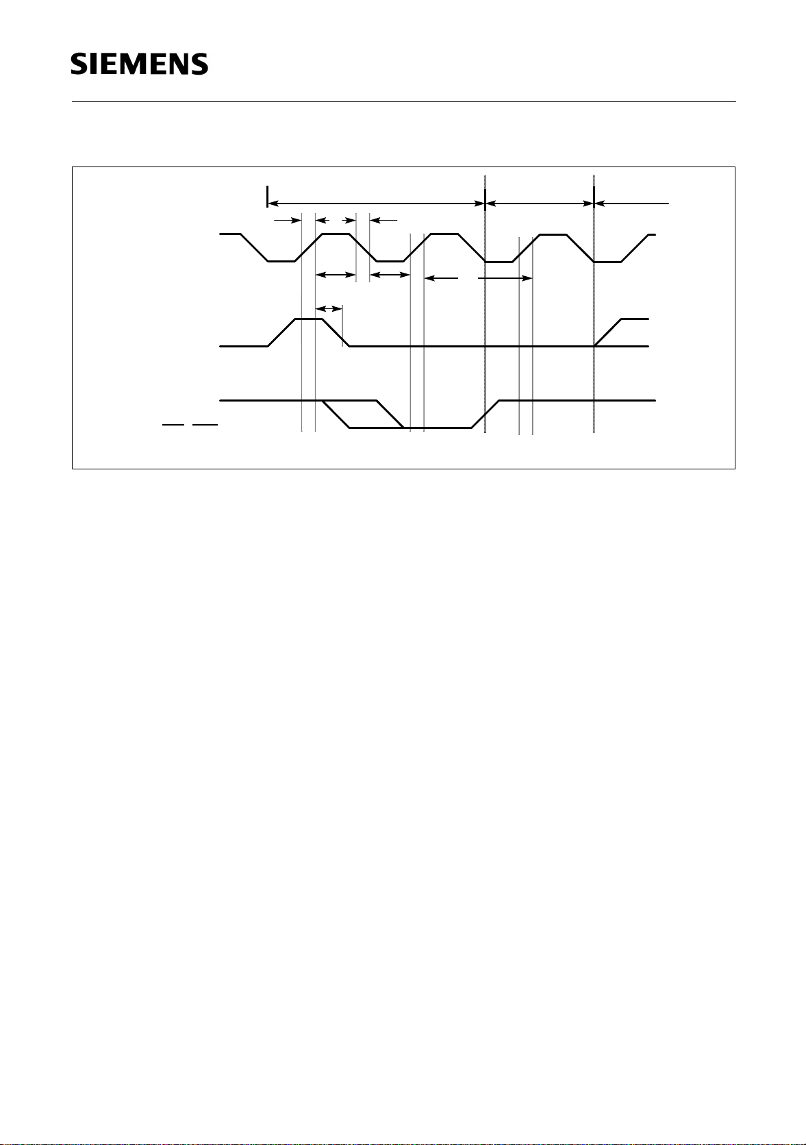
C164CI
3)
4)
CLKOUT
ALE
Command
RD
, WR
Running cycle
t
32
t
t
1)
t
33
30
t
34
31
2)
MUX/Tristate
t
29
Figure 15
CLKOUT Timing
Notes
1)
Cycle as programmed, including MCTC waitstates (Example shows 0 MCTC WS).
2)
The leading edge of the respect iv e co m mand depends on RW-delay.
3)
Multiplexed bus modes have a MU X waits tate added aft er a bus cycle, and an a ddit ional MTTC wa its tate may
be inserted here.
For a multiplexed bus with MT TC w ait s ta te this delay is 2 CLKOUT cycles.
4)
The next external bus cycle may start here.
Semiconductor Group 52 1998-02
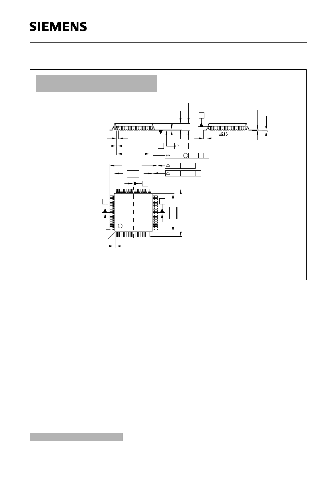
Package Outline
Plastic Package, P-MQFP-80-1 (SMD)
(Plastic Metric Quad Flat Package)
C164CI
0.65
±0.08
0.3
12.35
17.2
1)
14
D
A
80
Index Marking
1) Does not include plastic or metal protrusions of 0.25 max per side
1
0.6x45˚
C
B
+0.1
-0.05
2.45 max
2
0.25 min
0.1
M
0.12
0.2
A-B
0.2
A-B
1)
17.2
14
A-B
D
H
D
80x
HD
4x
C
0.88
80x
-0.02
+0.08
0.15
7˚max
Figure 16
Sorts of Packing
Package outlines for tubes, trays etc. are contained in our
Data Book “Package Information”.
SMD = Surface Mounted Device
Dimensions in mm
Semiconductor Group 53 1998-02
 Loading...