

Page 1
LC-60E77UN/LC-65E77UM/LC-C6077UN/LC-C6577UM
SERVICE MANUAL
No. S99C6LC60E77U
LCD COLOR TELEVISION
LC-60E77UN
LC-65E77UM
LC-C6077UN
MODELS
In the interests of user-safety (Required by safety regulations in some countries) the set should be restored to its original condition and only parts identical to those specified should be used.
LC-C6577UM
CONTENTS
SAFETY PRECAUTION
IMPORTANT SERVICE SAFETY
PRECAUTION.....................................................i
PRECAUTIONS A PRENDRE LORS DE
LA REPARATION...............................................ii
PRECAUTIONS FOR USING LEAD-FREE
SOLDER ........................................................... iii
CHAPTER 1. SPECIFICATIONS
[1] SPECIFICATIONS ......................................... 1-1
CHAPTER 2. OPERATION MANUAL
[1] Parts Name .................................................... 2-1
CHAPTER 3. DIMENSIONS
[1] DIMENSIONS
(LC-60E77UN/LC-C6077UN)......................... 3-1
[2] DIMENSIONS
(LC-65E77UM/LC-C6577UM) ........................ 3-2
CHAPTER 4. REMOVING OF MAJOR PARTS
[1] REMOVING OF MAJOR PARTS
(LC-60E77UN/LC-C6077UN)......................... 4-1
[2] REMOVING OF MAJOR PARTS
(LC-65E77UM/LC-C6577UM) ........................ 4-7
[2]
PUBLIC MODE SETTING PROCEDURE
CHAPTER 6. TROUBLESHOOTING TABLE
[1] TROUBLESHOOTING TABLE ......................6-1
CHAPTER 7. MAJOR IC INFORMATIONS
[1] MAJOR IC INFORMATIONS .........................7-1
CHAPTER 8. OVERALL WIRING/SYSTEM BLOCK
DIAGRAM
[1] OVERALL WIRING DIAGRAM
(LC-60E77UN/LC-C6077UN) ........................8-1
[2] OVERALL WIRING DIAGRAM
(LC-65E77UM/LC-C6577UM) .......................8-2
[3] SYSTEM BLOCK DIAGRAM .........................8-3
CHAPTER 9. PRINTED WIRING BOARD ASSEMBLIES
[1] KEY Unit, R/C, LED Unit Unit ........................9-1
[2] MAIN Unit ......................................................9-2
CHAPTER 10. SCHEMATIC DIAGRAM
[1] DESCRIPTION OF SCHEMATIC
DIAGRAM....................................................10-1
[2] SCHEMATIC DIAGRAM..............................10-2
.......5-18
CHAPTER 5. ADJUSTMENT
[1] ADJUSTMENT PROCEDURE ....................... 5-1
Parts marked with " " are important for maintaining the safety of the set. Be sure to replace these parts with specified ones for maintaining the
safety and performance of the set.
Parts Guide
This document has been published to be used for
after sales service only.
The contents are subject to change without notice.
Page 2
LC-60E77UN/LC-65E77UM/LC-C6077UN/LC-C6577UM
LC60E77UN
SAFETY PRECAUTION
Service Manual
IMPORTANT SERVICE SAFETY PRECAUTION
Service work should be performed only by qualified service technicians who are thoroughly familiar with all safety checks and the
servicing guidelines which follow:
WARNING
1. For continued safety, no modification of any circuit should be
attempted.
2. Disconnect AC power before servicing.
CAUTION: FO R CO NT IN U ED PROTECTION
AGAINST A RISK OF FIRE REPLACE ONLY WITH
SAME TYPE FUSE.
F101 (125V 6.3A) (LC-60E77UN/LC-C6077UN)
F102 (125V 6.3A) (LC-60E77UN/LC-C6077UN)
F301 (125V 6.3A) (LC-60E77UN/LC-C6077UN)
F302 (125V 6.3A) (LC-60E77UN/LC-C6077UN)
F7000 (250V 12A) (LC-60E77UN/LC-C6077UN)
F101 (250V 4A) (LC-65E77UM/LC-C6577UM)
F102 (250V 1A) (LC-65E77UM/LC-C6577UM)
F103 (250V 4A) (LC-65E77UM/LC-C6577UM)
F401 (250V 4A) (LC-65E77UM/LC-C6577UM)
F402 (250V 1A) (LC-65E77UM/LC-C6577UM)
F403 (250V 4A) (LC-65E77UM/LC-C6577UM)
F7000 (250V 12A) (LC-65E77UM/LC-C6577UM)
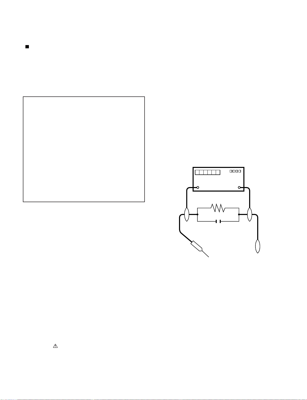
• Plug the AC cord directly into a 120 volt AC outlet.
• Using two clip leads, connect a 1.5k ohm, 10 watt resistor paral-
leled by a 0.15µF capacitor in series with all exposed metal cabinet
parts and a known earth ground, such as electrical conduit or electrical ground connected to an earth ground.
• Use an AC voltmeter having with 5000 ohm per volt, or higher, sensitivity or measure the AC voltage drop across the resistor.
• Connect the resistor connection to all exposed metal parts having a
return to the chassis (antenna, metal cabinet, screw heads, knobs
and control shafts, escutcheon, etc.) and measure the AC voltage
drop across the resistor.
All checks must be repeated with the AC cord plug connection
reversed. (If necessary, a nonpolarized adaptor plug must be used
only for the purpose of completing these checks.)
Any reading of 0.75 Vrms (this corresponds to 0.5 mA rms AC.) or
more is excessive and indicates a potential shock hazard which
must be corrected before returning the monitor to the owner.
DVM
AC SCALE
1.5k ohm
10W
BEFORE RETURNING THE RECEIVER (Fire &
Shock Hazard)
Before returning the receiver to the user, perform the following
safety checks:
3. Inspect all lead dress to make certain that leads are not pinched,
and check that hardware is not lodged between the chassis and
other metal parts in the receiver.
4. Inspect all protective devices such as non-metallic control knobs,
insulation materials, cabinet backs, adjustment and compartment
covers or shields, isolation resistor-capacitor networks, mechanical
insulators, etc.
5. To be sure that no shock hazard exists, check for leakage current in
the following manner.
///////////////////////////////////////////////////////////////////////////////////////////////////////////////////////////////////////////////////////////////////////////////////////////////////////////////////////////////////////////
TO EXPOSED
METAL PARTS
0.15µF
TEST PROBE
CONNECT TO
KNOWN EARTH
GROUND
SAFETY NOTICE
Many electrical and mechanical parts in LCD color television have
special safety-related characteristics.
These characteristics are often not evident from visual inspection, nor
can protection afforded by them be necessarily increased by using
replacement components rated for higher voltage, wattage, etc.
Replacement parts which have these special safety characteristics are
identified in this manual; electrical components having such features
are identified by " " and shaded areas in the Replacement Parts List
and Schematic Diagrams.
///////////////////////////////////////////////////////////////////////////////////////////////////////////////////////////////////////////////////////////////////////////////////////////////////////////////////////////////////////////
For continued protection, replacement parts must be identical to those
used in the original circuit.
The use of a substitute replacement parts which do not have the same
safety characteristics as the factory recommended replacement parts
shown in this service manual, may create shock, fire or other hazards.
i
Page 3
LC-60E77UN/LC-65E77UM/LC-C6077UN/LC-C6577UM
PRECAUTIONS A PRENDRE LORS DE LA REPARATION
Ne peut effectuer la réparation qu' un technicien spécialisé qui s'est parfaitement accoutumé à toute vérification de sécurité et aux
conseils suivants.
AVERTISSEMENT
•
1.
N'entreprendre aucune modification de tout circuit. C'est dangereux.
2.
Débrancher le récepteur avant toute réparation.
CAUTION: F OR C O NT I NU ED PROTECTION
AGAINST A RISK OF FIRE R EPLACE ONLY WITH
SAME TYPE FUSE.
F101 (125V 6.3A) (LC-60E77UN/LC-C6077UN)
F102 (125V 6.3A) (LC-60E77UN/LC-C6077UN)
F301 (125V 6.3A) (LC-60E77UN/LC-C6077UN)
F302 (125V 6.3A) (LC-60E77UN/LC-C6077UN)
F7000 (250V 12A) (LC-60E77UN/LC-C6077UN)
F101 (250V 4A) (LC-65E77UM/LC-C6577UM)
F102 (250V 1A) (LC-65E77UM/LC-C6577UM)
F103 (250V 4A) (LC-65E77UM/LC-C6577UM)
F401 (250V 4A) (LC-65E77UM/LC-C6577UM)
F402 (250V 1A) (LC-65E77UM/LC-C6577UM)
F403 (250V 4A) (LC-65E77UM/LC-C6577UM)
F7000 (250V 12A) (LC-65E77UM/LC-C6577UM)
Brancher le cordon d'alimentation directem-ent à une prise de courant de 120V. (Ne pas utiliser de transformateur d'isolation pour
cet essai).
•
A l'aide de deux fils à pinces, brancher une résistance de 1.5 kΩ
10 watts en parallèle avec un condensateur de 0.15µF en série
avec toutes les pièces métalliques exposées du coffret et une terre
connue comme une conduite électrique ou une prise de terre
branchée à la terre.
•
Utiliser un voltmètre CA d'une sensibilité d'au moins 5000Ω/V pour
mesurer la chute de tension en travers de la résistance.
•
Toucher avec la sonde d'essai les pièces métalliques exposées qui
présentent une voie de retour au châssis (antenne, coffret métallique, tête des vis, arbres de commande et des boutons, écusson,
etc.) et mesurer la chute de tension CA en-travers de la résistance.
Toutes les vérifications doivent être refaites après avoir inversé la
fiche du cordon d'alimentation. (Si nécessaire, une prise
d'adpatation non polarisée peut être utilisée dans le but de terminer ces vérifications.)
La tension de pointe mesurèe ne doit pas dépasser 0.75V (correspondante au courant CA de pointe de 0.5mA).
Dans le cas contraire, il y a une possibilité de choc électrique qui
doit être supprimée avant de rendre le récepteur au client.
VERIFICATIONS CONTRE L'INCEN-DIE ET LE
CHOC ELECTRIQUE
Avant de rendre le récepteur à l'utilisateur, effectuer les vérifications suivantes.
3.
Inspecter tous les faisceaux de câbles pour s'assurer que les fils
ne soient pas pincés ou qu'un outil ne soit pas placé entre le châssis et les autres pièces métalliques du récepteur.
4.
Inspecter tous les dispositifs de protection comme les boutons de
commande non-métalliques, les isolants, le dos du coffret, les couvercles ou blindages de réglage et de compartiment, les réseaux
de résistancecapacité, les isolateurs mécaniques, etc.
5.
S'assurer qu'il n'y ait pas de danger d'électrocution en vérifiant la
fuite de courant, de la facon suivante:
/////////////////////////////////////////////////////////////////////////////////////////////////////////////////////////////////////////////////////////////////////////////////////////////////////////////////////////////////////////////
AUX PIECES
METALLIQUES
EXPOSEES
DVM
ECHELLE CA
1.5k ohm
10W
0.15
µ
SONDE D'ESSAI
F
BRANCHER A UNE
TERRE CONNUE
AVIS POUR LA SECURITE
De nombreuses pièces, électriques et mécaniques, dans les téléviseur ACL présentent des caractéristiques spéciales relatives à la sécurité, qui ne sont souvent pas évidentes à vue. Le degré de protection ne peut pas être nécessairement augmentée en utilisant des
pièces de remplacement étalonnées pour haute tension, puissance,
etc.
Les pièces de remplacement qui présentent ces caractéristiques sont
identifiées dans ce manuel; les pièces électriques qui présentent ces
particularités sont identifiées par la marque " " et hachurées dans la
liste des pièces de remplacement et les diagrammes schématiques.
/////////////////////////////////////////////////////////////////////////////////////////////////////////////////////////////////////////////////////////////////////////////////////////////////////////////////////////////////////////////
Pour assurer la protection, ces pièces doivent être identiques à celles
utilisées dans le circuit d'origine. L'utilisation de pièces qui n'ont pas
les mêmes caractéristiques que les pièces recommandées par l'usine,
indiquées dans ce manuel, peut provoquer des électrocutions, incendies, radiations X ou autres accidents.
ii
Page 4
LC-60E77UN/LC-65E77UM/LC-C6077UN/LC-C6577UM
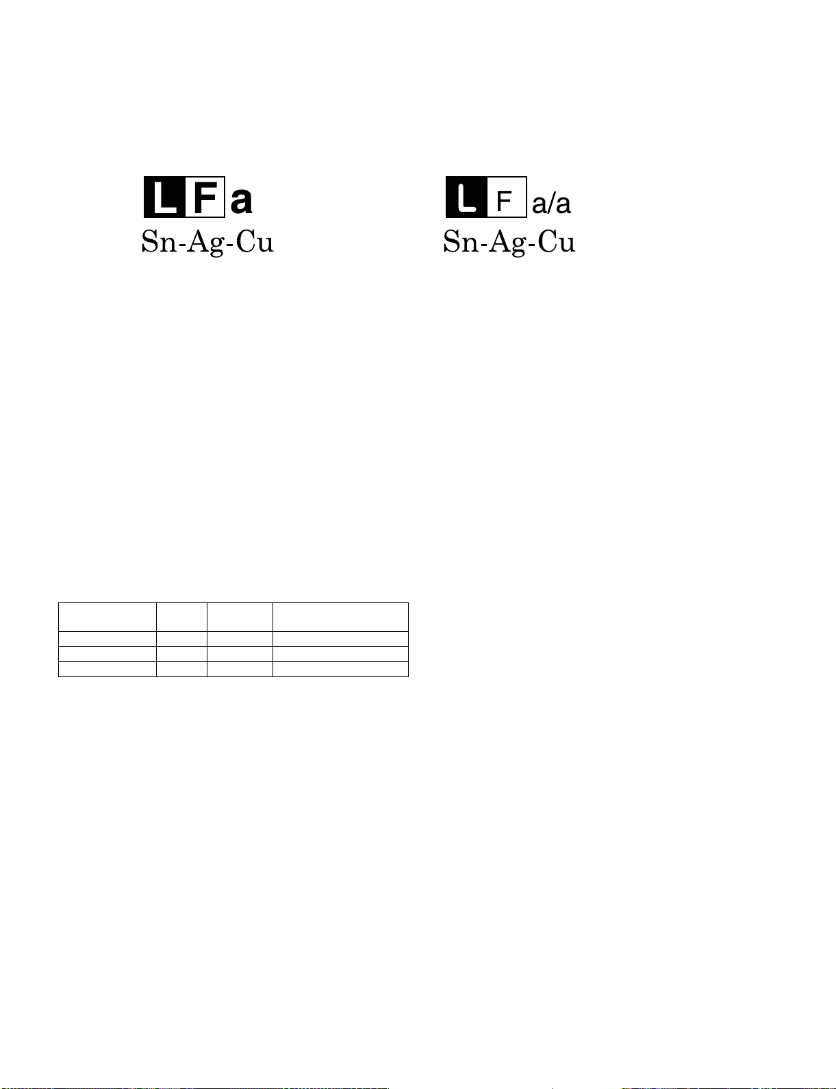
PRECAUTIONS FOR USING LEAD-FREE SOLDER
Employing lead-free solder
• “PWBs” of this model employs lead-free solder. The LF symbol indicates lead-free solder, and is attached on the PWBs and service manuals. The
alphabetical character following LF shows the type of lead-free solder.
Example:
Indicates lead-free solder of tin, silver and copper. Indicates lead-free solder of tin, silver and copper.
Using lead-free wire solder
• When fixing the PWB soldered with the lead-free solder, apply lead-free wire solder. Repairing with conventional lead wire solder may cause damage or accident due to cracks.
As the melting point of lead-free solder (Sn-Ag-Cu) is higher than the lead wire solder by 40 °C, we recommend you to use a dedicated soldering
bit, if you are not familiar with how to obtain lead-free wire solder or soldering bit, contact our service station or service branch in your area.
Soldering
• As the melting point of lead-free solder (Sn-Ag-Cu) is about 220 °C which is higher than the conventional lead solder by 40 °C, and as it has poor
solder wettability, you may be apt to keep the soldering bit in contact with the PWB for extended period of time. However, Since the land may be
peeled off or the maximum heat-resistance temperature of parts may be exceeded, remove the bit from the PWB as soon as you confirm the
steady soldering condition.
Lead-free solder contains more tin, and the end of the soldering bit may be easily corroded. Make sure to turn on and off the power of the bit as
required.
If a different type of solder stays on the tip of the soldering bit, it is alloyed with lead-free solder. Clean the bit after every use of it.
When the tip of the soldering bit is blackened during use, file it with steel wool or fine sandpaper.
• Be careful when replacing parts with polarity indication on the PWB silk.
Lead-free wire solder for servicing
PARTS CODE
ZHNDAi123250E BL J φ0.3mm 250g (1roll)
ZHNDAi126500E BK J φ0.6mm 500g (1roll)
ZHNDAi12801KE BM J φ1.0mm 1kg (1roll)
PRICE
RANK
PART
DELIVERY
DESCRIPTION
iii
Page 5
LC-60E77UN/LC-65E77UM/LC-C6077UN/LC-C6577UM
LC60E77UN
CHAPTER 1. SPECIFICATIONS
Service Manual
[1] SPECIFICATIONS
Item Model: LC-60E77UN/LC-C6077UN Model: LC-65E77UM/LC-C6577UM
LCD
panel
1
Size 60" Class (60
/32" Diagonal)
Resolution 2,073,600 pixels (1,920x 1,080)
65" Class (64
TV-standard (CCIR) American TV Standard ATSC/NTSC System
VHF/UHF VHF 2-13ch, UHF 14-69ch
CATV 1-135ch (non-scrambled channel only)
TV
Function
Receiving
Channel
Digital Terrestrial
Broadcast (8VSB)
Digital cable
*1
(64/256 QAM)
2-69ch
1-135ch (non-scrambled channel only)
Audio multiplex BTSC System
Audio out 10W x 2
INPUT 1 AV in, COMPONENT in
INPUT 2 COMPONENT in, S-VIDEO in
INPUT 4 ANALOG RGB (PC) in (15-pin mini D-sub female connector), Audio in (Ø 3.5 mm jack)
INPUT 6 HDMI in with HDCP, Audio in (Ø 3.5 mm jack)
INPUT 7 HDMI in with HDCP
INPUT 8 HDMI in with HDCP
Rear
ANT/CABLE 75 Ω Unbalance, F Type x 1 for Analog (VHF/UHF/CATV) and Digital (AIR/CABLE)
Terminals
AUDIO Audio in (Ø 3.5 mm jack)
DIGITAL AUDIO OUTPUT
Optical Digital audio output x 1 (PCM/Dolby Digital)
OUTPUT Audio out
RS-232C 9-pin D-sub male connector
INPUT 3 AV in
Side
INPUT 5 HDMI in with HDCP
SERVICE Software update
OSD language English/French/Spanish
Power Requirement AC 120 V, 60 Hz
Power Consumption 390 W (0.4 W Standby with AC 120 V) 525 W (0.4 W Standby with AC 120 V)
Weight
Dimension
*2
(WxHxD)
Operating temperature
*1
Emergency alert messages via Cable are unreceivable.
*2
The dimensional drawings are shown on the inside back cover.
TV + stand 92.6 lbs./42.0 kg 110.2 lbs./50.0 kg
TV only 81.6 lbs./37.0 kg 99.2 lbs./45.0 kg
TV+stand
565/8x3729/64x179/16inch
TV only 56
5
/8x3511/
45
x 4
/64inch
64
603/4x3927/32x179/16inch
3
/4x3739/64x445/64inch
60
+ 32°F to +104°F (0°C to +40°C)
• As part of policy of continuous improvement, SHARP reserves the right to make design and specification changes for
product improvement without prior notice. The performance specification figures indicated are nominal values of production
units. There may be some deviations from these values in individual units.
33
/64" Diagonal)
Optional Accessory
The listed optional accessory is available for the Liquid
Crystal Television. Please purchase it at your nearest shop.
• Additional optional accessories may be available in the near
future. When purchasing, please read the newest catalogue for
compatibility and check the availability.
1 – 1
Part name Model number
AN-52AG4
Wall mount bracket
(for LC-60E77UN/LC-C6077UN)
AN-65AG1
(for LC-65E77UM/LC-C6577UM)
Page 6
LC-60E77UN/LC-65E77UM/LC-C6077UN/LC-C6577UM
LC60E77UN
CHAPTER 2. OPERATION MANUAL
[1] Parts Name
TV (Front)
TV (Rear/Side)
*2
POWER
button
Service Manual
Remote control sensor
OPC sensor
OPC indicator
POWER indicator
*
* OPC: Optical Picture Control
AC INPUT
terminal
*3
MENU
button
INPUT
button
Channel
buttons
(CH /)
Volume
buttons
(VOL /)
*1
INPUT 5
terminal
(HDMI)
INPUT 3
terminals
SERVICE
terminal
LC-60E77UN/
LC-C6077UN
INPUT 4 terminal (PC-IN)
AUDIO terminal (shared for INPUT 4 and INPUT 6)*4
INPUT 6 terminal (HDMI)
LC-65E77UM/
LC-C6577UM
*1
INPUT 7 terminal
(HDMI)
INPUT 8 terminal
(HDMI)
DIGITAL AUDIO
OUTPUT terminal
AUDIO OUTPUT
terminals
Antenna/Cable in
INPUT 1 terminals
INPUT 2 terminals
RS-232C terminal
*1 External equipment connection.
*2 Button operations.
*3 Connecting the AC cord.
*4 Details on the PC Audio Select function.
• The illustrations in this operation manual are for explanation purposes and may vary slightly from the actual operations.
• The examples used throughout this manual are based on the LC-65E77UM model.
2 – 1
Page 7
1. Remote Control Unit (LC-60E77UN/LC-65E77UM)
LC-60E77UN/LC-65E77UM/LC-C6077UN/LC-C6577UM
Remote Control Unit
117
2
3
4
5
6
7
8
9
10
11
12
13
14
15
16
18
19
20
21
22
23
24
25
26
27
28
29
30
1 TV POWER: Switch the TV power on or enter standby.
2 DISPLAY: Display the channel information.
3 SOURCE POWER: Turns the power of the external equipment
on and off.
4 External equipment operational buttons: Operate the external
equipment.
50–9: Set the channel.
6 • (DOT):
7 INPUT: Select a TV input source. (TV, INPUT 1, INPUT 2, INPUT 3,
INPUT 4, INPUT 5, INPUT 6, INPUT 7, INPUT 8)
8VOL/ : Set the volume.
9 POWER SAVING: Select Power Saving settings.
10 FREEZE: Set the still image. Press again to return to normal
screen.
11 EXIT: Turn off the menu screen.
12 OPTION: Display the AQUOS LINK MENU screen. This button
will function only when AQUOS LINK is used.
13 REC STOP: Stops one touch recording. This button will function
onlywhenAQUOSLINKisused.
14 SLEEP: Set the sleep timer.
15 SURROUND: Select Surround settings.
16 AUDIO: Selects the MTS/SAP or the audio mode during multi-
channel audio broadcasts.
17 FUNCTION: Switches the remote control for TV, CBL/SAT, VCR,
DVD and AUDIO operation. Indicator lights up for the current
mode.
* To enter the code registration mode, you need to press
FUNCTION and DISPLAY at the same time.
18 LIGHT : When this button is pressed, some buttons (for
example, VOL /
light. The lighting will turn off if no operations are performed within
about 5 seconds. This button is used for performing operations in
low-light situations.
19 VIEW MODE: Select the screen size.
20 ENT: Jumps to a channel after selecting with the 0–9 buttons.
21 FLASHBACK: Return to the previous channel or external input
mode.
22 CH / : Select the channel.
23 MUTE: Mute the sound.
24 MENU: Display the menu screen.
25 ///,ENTER: Select a desired item on the screen.
26 RETURN: Return to the previous menu screen.
27 FAVORITE CH
A, B, C, D: Select 4 preset favorite channels in 4 different
categories.
While watching, you can toggle the selected channels by pressing
A, B, C and
28 FAVORITE: Set the favorite channels.
29 CC: Display captions from a closed-caption source.
30 AV MODE: Select an audio or video setting.
(When the input source is TV, INPUT 1, 2 or 3: STANDARD,
MOVIE, GAME, USER, AUTO, DYNAMIC (Fixed), DYNAMIC.
When the input source is INPUT 4, 5, 6, 7 or 8: STANDARD,
MOVIE, GAME, PC, USER, AUTO, DYNAMIC (Fixed), DYNAMIC)
and CH / ) on the remote control unit will
D.
• When using the remote control unit, point it at the TV.
2 – 2
Page 8
LC-60E77UN/LC-65E77UM/LC-C6077UN/LC-C6577UM
2. Remote Control Unit (LC-C6077UN/LC-C6577UM)
14
6
8
1
15
5
11
4
2
7
16
13
9
12
10
3
Changing Volume
You can change the volume by pressing VOL /on
the TV or on the remote control unit.
To increase the volume, press VOL .
•
To decrease the volume, press VOL .
•
20
Audio status
Output device
Speaker Variable sound Mute
When "Output Select" is set to "Variable", the indicator on
•
the screen changes as shown below.
Output Select
Fixed Variable
60
Details on the Output Select function.
•
MUTE
Mutes the current sound output.
Press MUTE.
" " will be displayed on the screen for 30 minutes, and
•
the sound is silenced.
POWER
You can turn on the TV or put it on standby by
pressing POWER on the TV or on the remote control
unit.
Changing Channels
You can change channels by pressing CH
• (DOT).
Examples:
To select a 1 or 2-digit channel number (e.g., Channel 5):
Press 5 ENT.
To select a 3-digit channel number (e.g., Channel 115):
Press 1 1 5 ENT.
To select a 4-digit channel number (e.g., Channel 22.1):
Press 2 2 • (DOT) 1 ENT.
When selecting a 1-digit channel number, it is not
•
necessary to press 0 before the number.
When you enter 0–9 only, channel selection will be made if
•
there is no operation within a few seconds.
If you push "0" by itself, nothing will happen.
•
Complete the above steps within a few seconds.
•
When you enter 0–9 and • (DOT), channel selection will be
•
made if there is no operation within a few seconds.
/
or 0–9,
FAVORITE CH
You can select 4 preset favorite channels in 4 different
categories.
Press A, B, C or D.
While watching the TV, you can toggle the selected
•
channels by pressing A, B, C and D.
Within 30 minutes of pressing MUTE, mute can be
•
canceled by pressing VOL
•
Mute will be canceled after 30 minutes have passed.
However, the TV will not suddenly output a loud sound as
the volume level is set to 0 automatically.
/ or MUTE.
Sleep Timer
Allows you to set a time when the TV automatically
switches to standby.
Press SLEEP.
•
The remaining time displays when the sleep timer has been set.
•
Each time you press SLEEP, the remaining time switches
as shown below.
Off306090120
•
When set, the time automatically starts counting down.
•
If you want to adjust the sleep timer, you can press SLEEP
twice then change the time setting.
•
When it is 5 minutes before the time expires, the remaining
time will start to keep appearing every minute.
•
Select "Off" by pressing SLEEP to cancel the sleep timer.
•
The TV will enter standby when the remaining time reaches 0.
•
When the sleep timer is set, its indicator on the TV lights red.
FLASHBACK
Press FLASHBACK to switch to the previously tuned
channel.
•
Press FLASHBACK again to switch back to the currently
tuned channel.
•
FLASHBACK will not work if no channel has been changed
after the TV is turned on.
Details of favorite channel settings.
•
2 – 3
Page 9

LC-60E77UN/LC-65E77UM/LC-C6077UN/LC-C6577UM
AV MODE
AV MODE gives you several viewing options to choose
from to best match the surrounding environment of the
TV, which can vary due to factors like room brightness,
type of program watched or the type of image input
from external equipment.
Press AV MODE. Current AV MODE displays.
•
Press AV MODE again before the mode displayed on the
screen disappears. The mode changes as shown below:
Example:
When the input source is TV, INPUT 1, 2 or 3 terminals
STANDARD MOVIE GAME USER [TV]
DYNAMIC DYNAMIC (Fixed) AUTO
Example:
When the input source is INPUT 4, 5, 6, 7 or 8
terminals
STANDARD MOVIE GAME PC USER[ ]
DYNAMIC DYNAMIC (Fixed) AUTO
STANDARD: For a highly defined image in a normal
lighting.
MOVIE: For a movie.
GAME: Lowers image brightness for easier viewing.
PC: For PC.
USER: Allows the user to customize settings as desired.
You can set the mode for each input source.
AUTO: Optimizes the image quality automatically based
on the room brightness and image signal.
DYNAMIC (Fixed): Changes the image and sound
settings to the factory preset values. No adjustments
are allowed.
DYNAMIC: For a clear-cut image emphasizing high
contrast, useful for sports viewing.
•
You can select a different AV MODE item for each input
mode. (For example, select STANDARD for TV input and
DYNAMIC for INPUT 1.)
•
When you play games, "GAME" is recommended for AV
MODE.
•
When AV MODE is set to "AUTO", part of the menu may
not be displayed correctly or the setting range of the menu
may be changed.
PC
9
Allows you to gain quick access to PC mode.
Press PC.
10
Operating On-Screen Display Menu
You can operate the on-screen display menu by using
the following buttons.
MENU: Displays the menu screen.
///,ENTER: Select a desired item on the
screen.
RETURN: Returns to the previous menu screen.
EXIT: Turns off the menu screen.
For operating the on-screen display menu, see “Menu
•
Operation Buttons”
11
AUDIO
MTS/SAP stereo mode
The TV has a feature that allows reception of sound
other than the main audio for the program. This feature
is called Multi-channel Television Sound (MTS). The TV
with MTS can receive mono sound, stereo sound
and Secondary Audio Programs (SAP). The SAP
feature allows a TV station to broadcast other
information, which could be audio in another language
or something completely different like weather
information.
You can enjoy Hi-Fi stereo sound or SAP broadcasts
where available.
Stereo broadcasts: View programs like live sporting
•
events, shows and concerts in dynamic stereo sound.
SAP broadcasts: Receive TV broadcasts in either MAIN or
•
SAP sound. MAIN sound: The normal program soundtrack
(either in mono or stereo). SAP sound: Listen to a second
language, supplementary commentary or other information.
(SAP is mono sound.)
If stereo sound is difficult to hear.
Obtain a clearer sound by manually switching to fixed
•
mono-sound mode.
You can change MTS as shown below to match the television
broadcast signal.
Press AUDIO to toggle between audio modes.
Examples: when receiving MTS and SAP
STEREO mode:
STEREO + SAP mode: ST(SAP)
MAIN + SAP mode: MAIN SAP
MONO mode: MONO
STEREO
MONO
SAP(ST) MONO
Digital broadcasting audio mode
The types of audio transmitted in a digital broadcast include
SURROUND as well as MONO and STEREO. In addition, it
is possible for multiple audio tracks to accompany a single
video track.
Press AUDIO to toggle between audio modes.
Example: when receiving Digital broadcasting
STEREO (Audio1) STEREO (Audio2)
SURROUND (Audio3)
MTS only operates while in TV mode.
•
FREEZE
12
Allows you to capture and freeze a moving image that
you are watching.
Press FREEZE.
A moving image is captured.
•
Press FREEZE again to cancel the function.
•
When this function is not available, "No displaying still
•
image available." will display.
The still image automatically goes out after 30 minutes.
•
•
If you are using the freeze function and a broadcast
activates the V-CHIP BLOCK, the freeze function will be
canceled and a V-CHIP BLOCK message will appear.
2 – 4
Page 10
LC-60E77UN/LC-65E77UM/LC-C6077UN/LC-C6577UM
f
13
INPUT
To view external source images, select the input
source
using INPUT on the remote control unit or on the TV.
Press INPUT.
1
A list of selectable sources appears.
•
Press INPUT again or press / to select the
2
input source.
•
An image from the selected source automatically displays.
•
Each time INPUT is pressed, the input source toggles.
•
If the corresponding input is not plugged in, you cannot change
the input. Be sure to connect the equipment beforehand.
•
External equipment connection.
•
Press PC to switch to an image from the PC.
DISPLAY
Displays channel information being viewed.
Press DISPLAY.
Closed Captions and Digital Closed Captions
Your TV is equipped with an internal Closed Caption
decoder. It allows you to view conversations, narration
and sound effects as subtitles on your TV. Closed
Captions are available on some TV programs and on
some VHS home video tapes at the discretion of the
program provider.
Digital Closed Caption service is a new caption service
available only on digital TV programs (also at the
discretion of the service provider). It is a more flexible
system than the original Closed Caption system,
because it allows for a variety of caption sizes and font
styles. When the Digital Closed Caption service is in
use, it will be indicated by the appearance of a 3-letter
abbreviation that also indicates the language of the
Digital Closed Captions: ENG (English), SPA (Spanish),
FRA (French) or other language codes.
Not all programs and VHS videotapes offer closed
captions. Please look for the “ ” symbol to ensure
that captions will be shown.
In the Closed Caption system, there can be more than
one caption service provided. Each is identified by its
own number. The “CC1” and “CC2” services display
subtitles of TV programs superimposed over the
program's picture.
CC
Press CC.
1
This will present the Closed Caption information display.
•
Press CC while the Closed Caption information is
2
still on the screen.
Press repeatedly until you select the desired closed
•
caption service.
Air DIGITAL
Air DIGITAL
22.1
22.1
Audio : MONO
Audio : MONO
:
Video 1080i (16:9)
:
Video 1080i (16:9)
CC 1/2 CC1:
CC 1/2 CC1:
Ratings : NONE
Ratings : NONE
:NONE
:NONE
Depending on the number of caption services in the
•
signal being received, you will see information such as
1/2 or 1/4 displayed.
1/2 means “the first of two services”.
Example:
If a program has three services (Digital CC(ENG), CC1
and Text1), the closed caption display will toggle in this
sequence:
1/3 ENG Of
The CC button keeps a record of the last service
•
selected in its memory.
If the last closed caption mode (e.g. 1/3ENG) you
selected is not available for the next program, or on
another channel, the closed caption service that is
available is automatically selected, and this service
appears in parentheses, e.g. “1/3(CC1)”.
Closed Caption services that appear in parentheses will
notbestoredintheCC button's memory as your last
selected service. Only services that you have selected
with the CC button are stored.
2/3 CC1 3/3 Text1
Closed Caption
information
Examples:
In a case where there are two closed caption
services provided (for instance, Digital CC(ENG)
and CC1), and Digital CC(ENG) is displayed as your
current selection, if Digital CC(ENG) is not broadcast
for the next program, the other closed caption
service, CC1, will be displayed in parentheses.
A closed caption service appears in parentheses
because the service you selected is not available
and a different service is displayed on your screen.
“1/1(CC1)” is displayed instead of “1/2/ENG”.
In the Closed Caption system, the “Text1” or “Text2”
services display text that is unrelated to the program
being viewed (e.g., weather or news). These services
are also superimposed over the program currently
being viewed.
•
When “Power Saving” is set to “Standard” or “Advanced”,
the Power Saving leaf icon appears on the channel
information window. Details of Power Saving settings.
•
Detailed closed caption settings.
•
When the program contains no closed caption, “--” displays
in the closed caption information.
•
If the language code, e.g. “ENG”, is not found on Digital TV
programs, “--” will be shown.
•
Four kinds of closed caption service (CC1, CC2, Text1,
Text2) are potentially available, but a broadcast may contain
none or only some of these services at the discretion of the
program provider.
2 – 5
Page 11
LC-60E77UN/LC-65E77UM/LC-C6077UN/LC-C6577UM
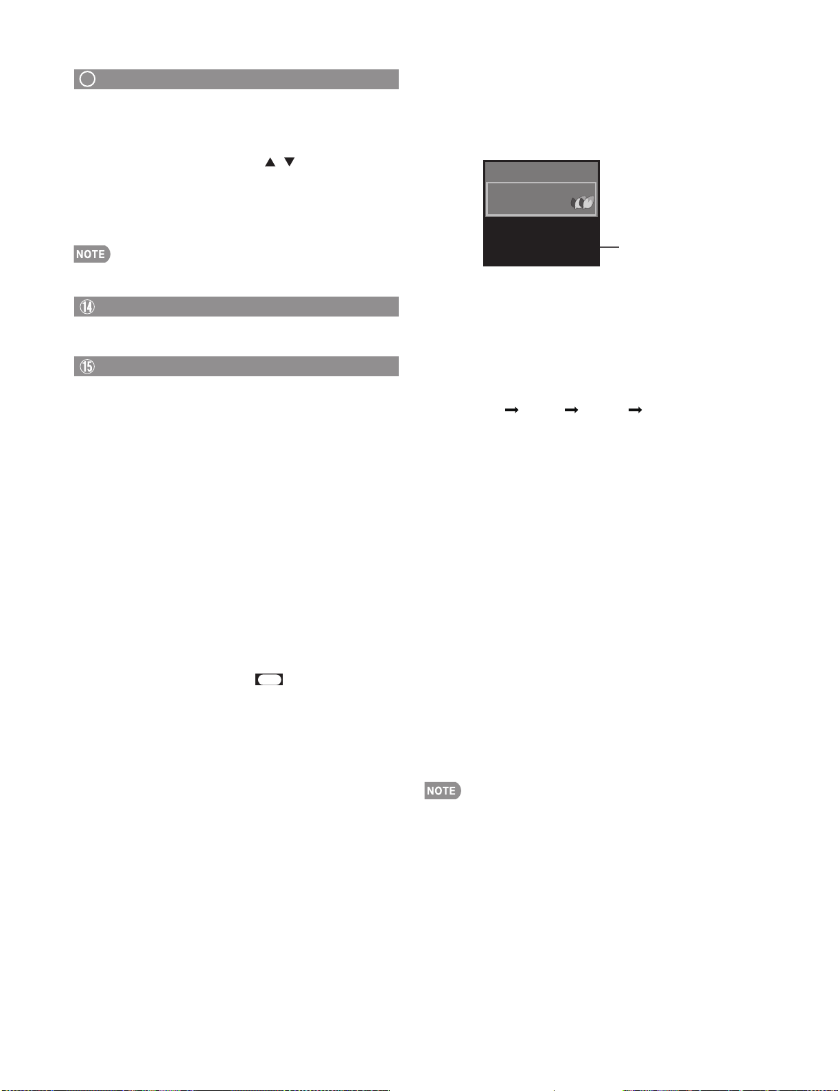
VIEW MODE
Youcanselectthescreensize.
Press VIEW MODE.
1
•
The View Mode menu displays.
•
The menu lists the View Mode options selectable for the type of video signal currently being received.
Press VIEW MODE or / while the View Mode menu is displayed to select a desired item on the menu.
2
•
You can sequentially select a View Mode that has its own aspect ratio.
For 4:3 programs
Example: Screen size images
Side Bar S.Stretch (Smart stretch) Zoom Stretch
Suitable for viewing
conventional 4:3 programs in
their normal format.
Suitable for stretching 4:3
programs to fill the screen.
Suitable for viewing widescreen 2.35:1 anamorphic
DVDs in full screen.
This mode is useful for 1.78:1
DVDs. When viewing 1.85:1
DVDs, stretch mode will still show
very thin black bands at the top
and bottom of the screen.
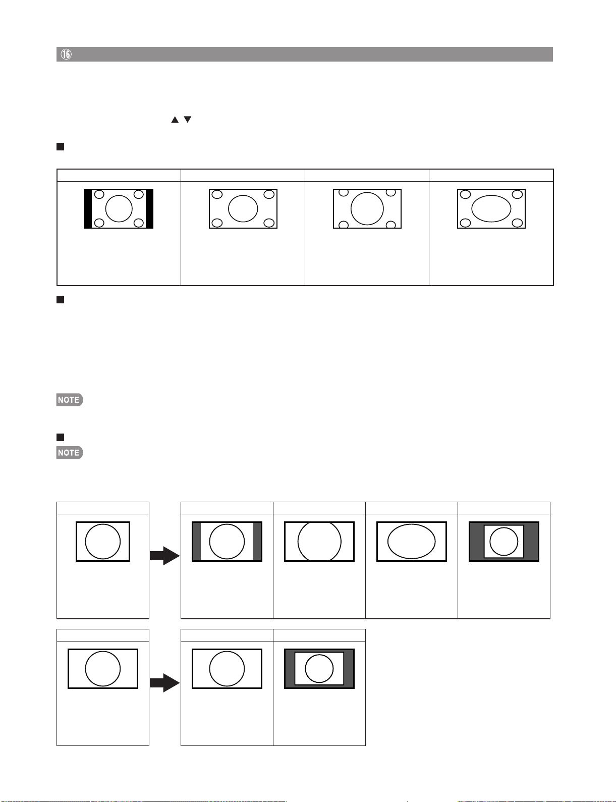
ForHDprograms
Stretch: Suitable for viewing wide-screen 1.78:1 aspect ratio program, stretch mode will still show very thin black bands at
the top and bottom of the screen.
Dot by Dot (1080i/p only): Detects the resolution of the signal and displays an image with the same number of pixels on
the screen.
Full Screen (720p only): You can select "Full Screen" only when receiving a 720p signal.
S.Stretch (Smart stretch): Suitable for stretching 4:3 programs to fill the screen.
Zoom: Suitable for viewing wide-screen 2.35:1 aspect-ratio programs in full screen.
When using Dot by Dot or Full Screen, it is possible to see noise or bars around different outer portions of the screen. Please
•
change view mode to correct this.
For PC input mode
Connect the PC before making adjustments.
•
Selectable screen size may vary with input signal type.
•
Example: Screen size images
Input signal Normal Zoom Stretch Dot by Dot
4:3
Input signal Stretch Dot by Dot
16:9 An image fully fills the
Keeps the original
aspectratioinafull
screen display.
screen.
For viewing
widescreen
programs. The top
and bottom of the
image is cropped.
Detects the resolution
of the signal and
displays an image with
the same number of
pixels on the screen.
2 – 6
An image fully fills the
screen.
Detects the resolution
of the signal and
displays an image with
the same number of
pixels on the screen.
Page 12
LC-60E77UN/LC-65E77UM/LC-C6077UN/LC-C6577UM
LC60E77UN
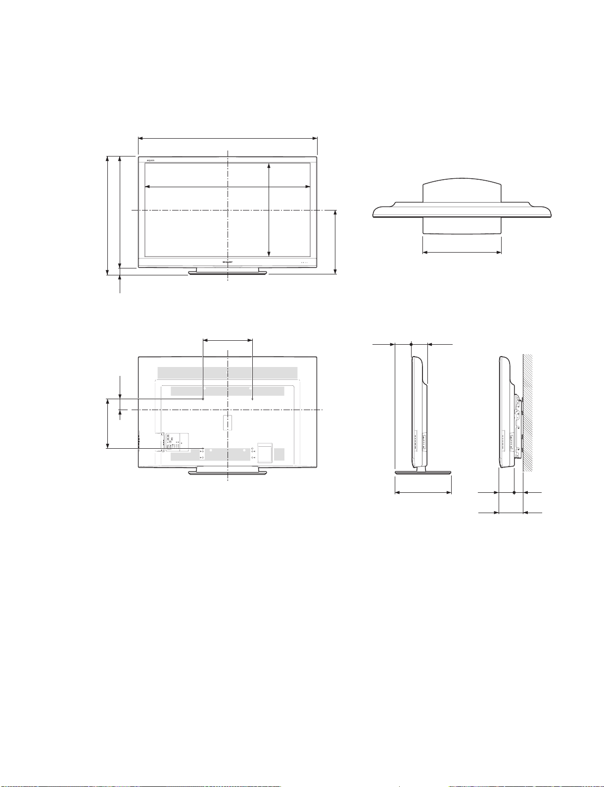
CHAPTER 3. DIMENSIONS
[1] DIMENSIONS (LC-60E77UN/LC-C6077UN)
5
/8(1438)
56
5217/32(1334)
(951)
(893)
64
64
/
/
29
37
11
35
32
/
9
(58)
2
5
8
/
29
(752)
Service Manual
(524)
64
/
41
20
Unit: inch (mm)
2421/32(626)
32
/
15
3
(400)
4
/
3
15
(88)
153/4(400)
55/
(135)
9
/16(446)
4
(119)
45
/
64
AN-52AG4
45
/
4
64
(119)
7
(186)
41
2
/
64
(67)
21
/
64
16
17
3 – 1
Page 13
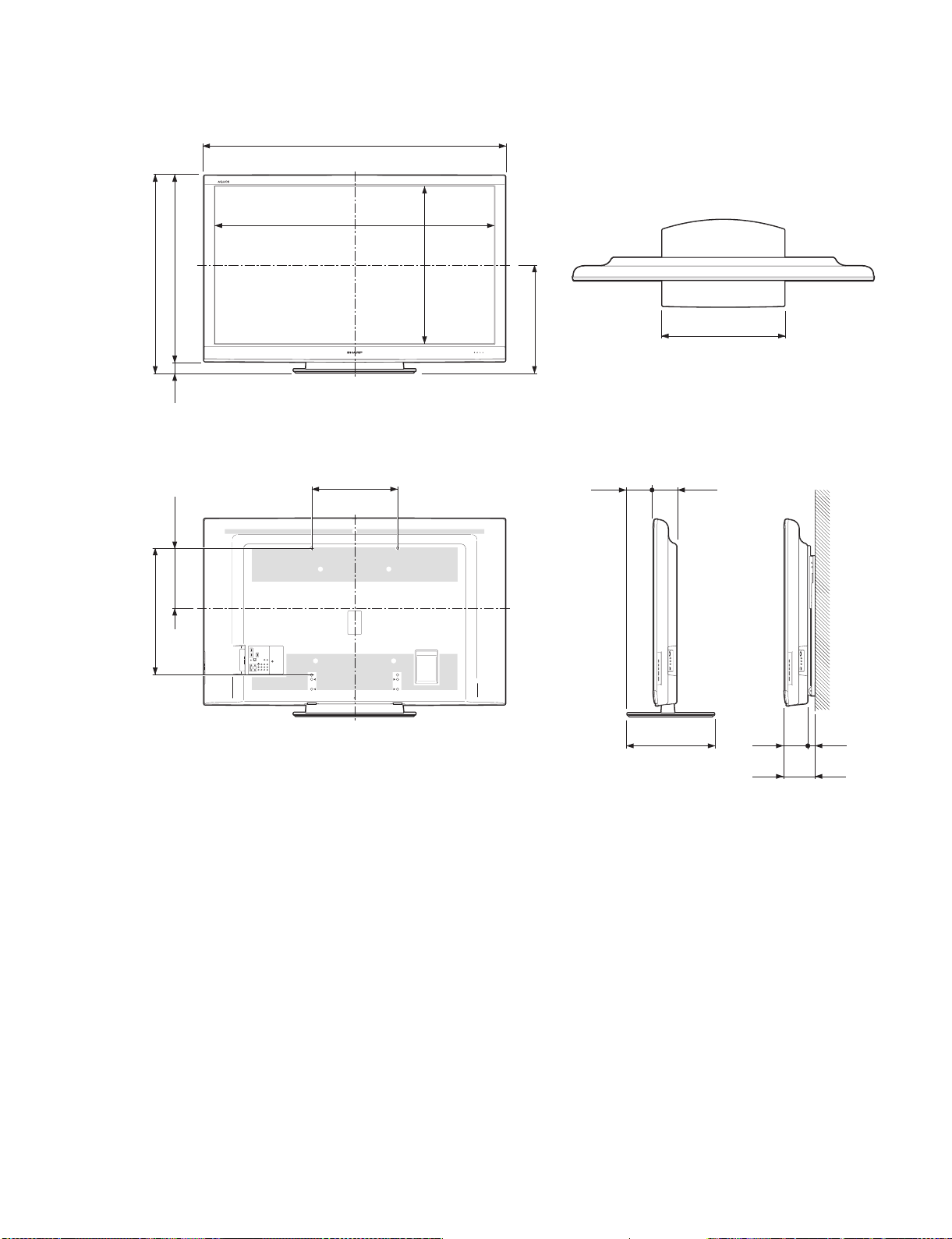
[2] DIMENSIONS (LC-65E77UM/LC-C6577UM)
603/4(1543)
13
/32(1432.6)
56
(955)
(1012)
64
32
/
/
39
27
37
39
4
/
1
(57)
2
64
/
49
31
(806.6)
LC-60E77UN/LC-65E77UM/LC-C6077UN/LC-C6577UM
Unit: inch (mm)
(553)
32
/
25
21
2421/32(626)
64
/
11
12
(650)
32
/
19
25
(309)
1721/64(440)
5
5
(135)
45
4
/
/
16
9
17
(119)
/16(446)
64
AN-65AG1
45
/
4
64
(119)
9
/
6
(156)
15
1
/
32
(37)
64
3 – 2
Page 14
LC-60E77UN/LC-65E77UM/LC-C6077UN/LC-C6577UM
LC60E77UN
CHAPTER 4. REMOVING OF MAJOR PARTS
Service Manual
[1] REMOVING OF MAJOR PARTS (LC-60E77UN/LC-C6077UN)
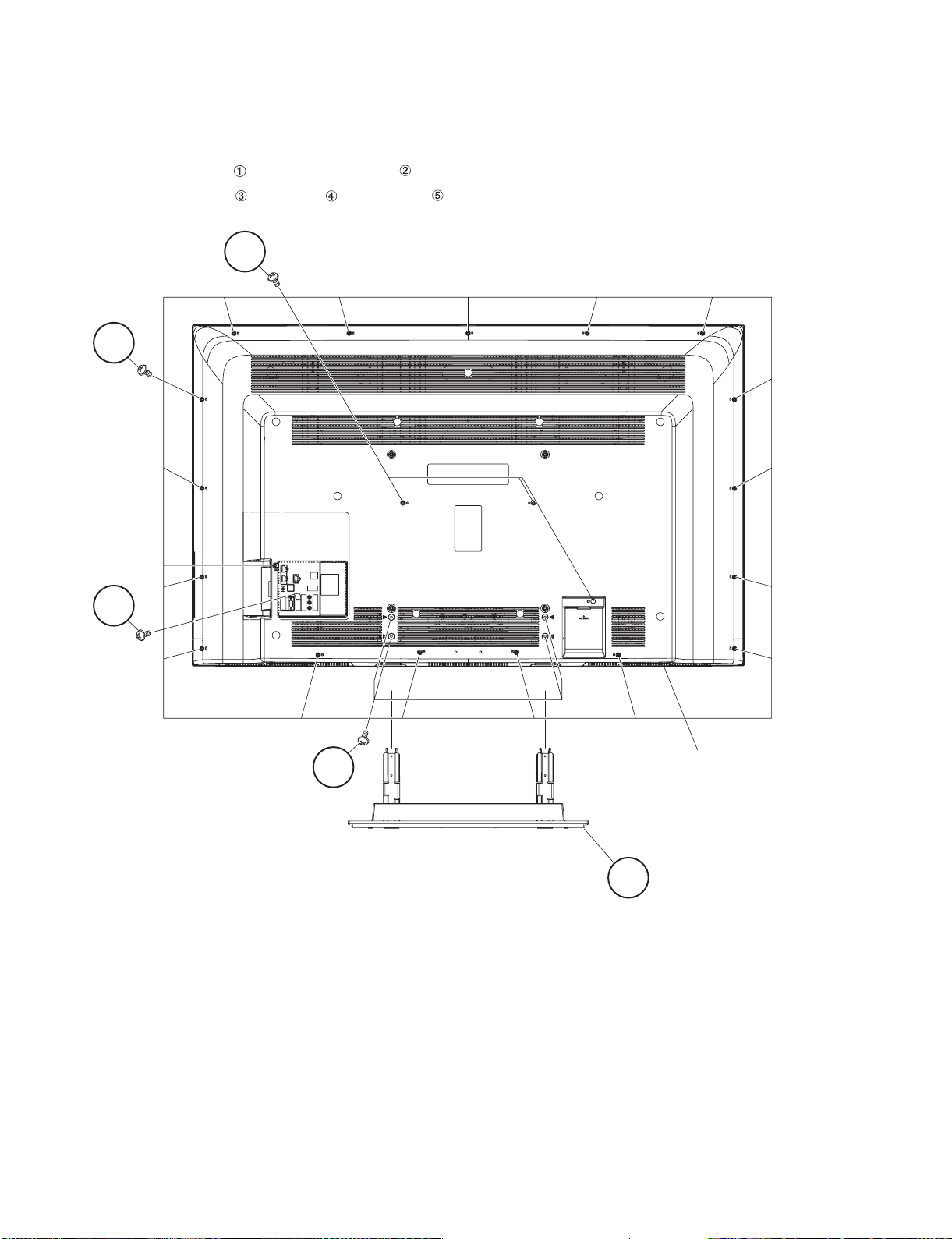
1. Removing of Stand Unit and Rear Cabinet Ass’y.
1. Remove the 4 lock screws and detach the Stand Unit .
2. Remove the 3 lock screws , 1 lock screw , 18 lock screws and detach the Rear Cabinet Ass’y.
3
5
4
1
Rear Cabinet Ass'y
2 Stand Unit
4 – 1
Page 15
LC-60E77UN/LC-65E77UM/LC-C6077UN/LC-C6577UM
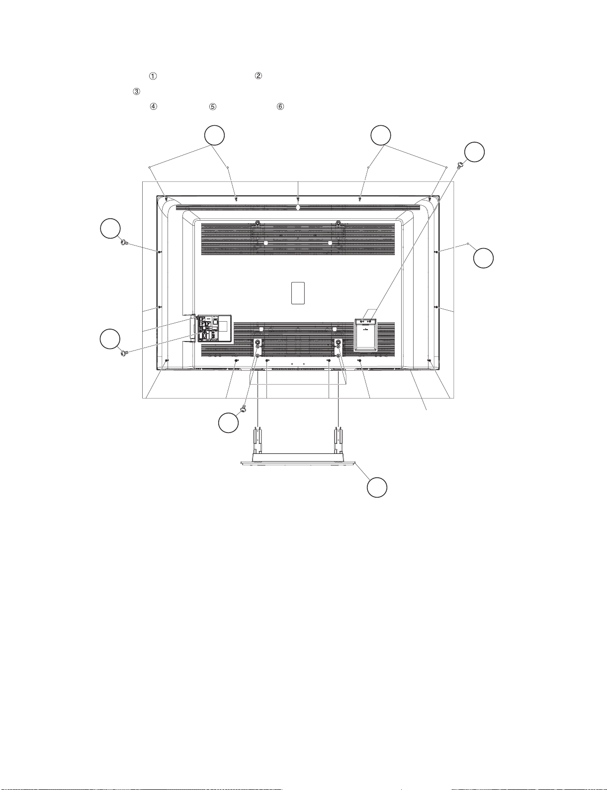
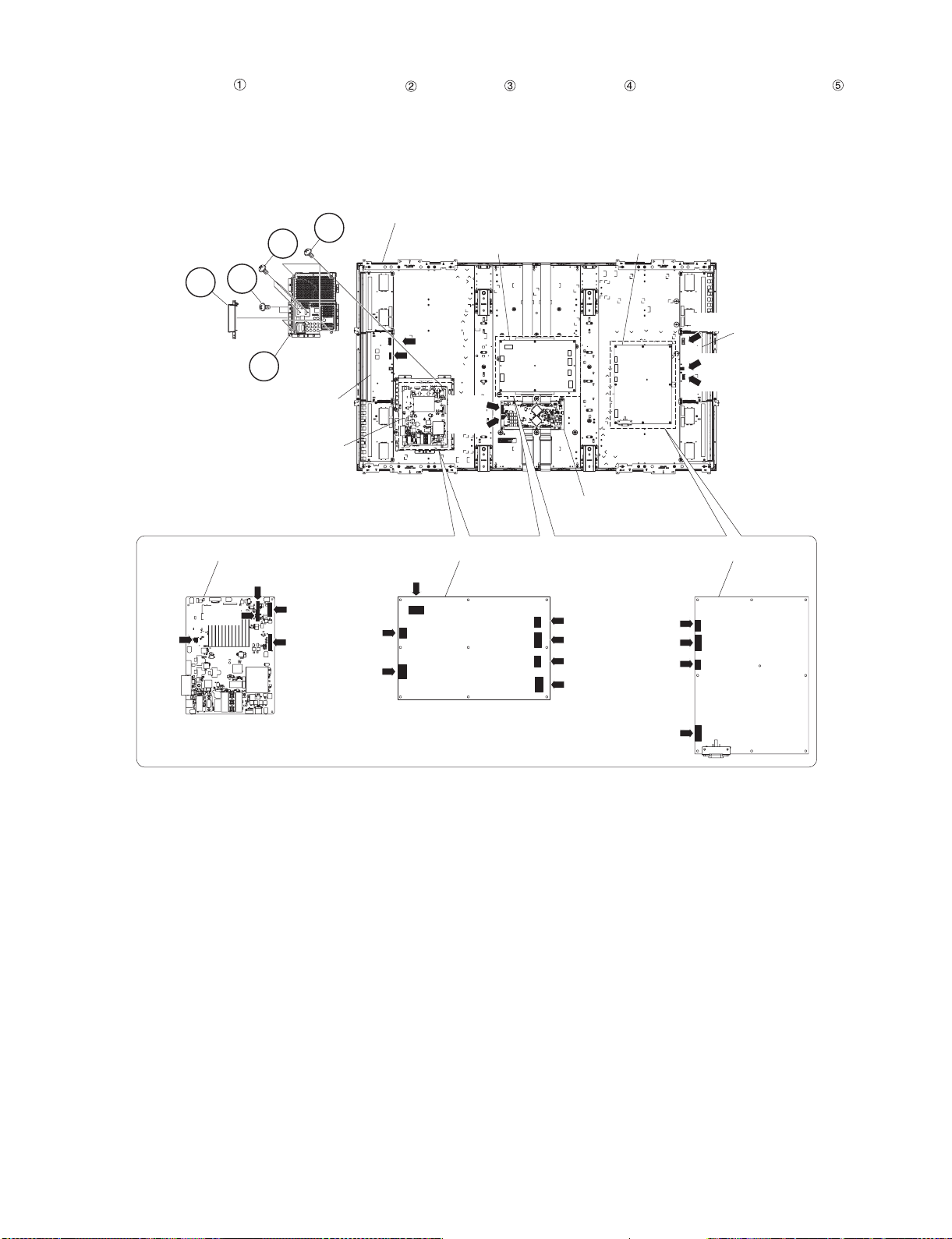
2. Removing of Speaker-L/R, KEY Unit, R/C, LED Unit, Front Cabinet Ass’y.
1. Disconnect the following connectors from the MAIN Unit. (RA, SP)
2. Detach the Speaker-L/R .
3. Disconnect the KEY Unit from the KEY Button Cover Ass’y and disconnect the connection cord from the KM Connector.
4. Detach the R/C, LED Unit . (RA)
5. Remove the 4 lock screws and 10 Hooks and detach the Front Cabinet Ass’y
Front Cabinet Ass'y
LCD Panel Module Unit Ass'y
Hook
Hook
Hook Hook
KEY Button
Cover Ass'y
2
3KEY Unit
[KM]
Hook
Hook
Hook
4R/C,LED Unit
[RA]
[RA] [SP]
5 5
5 5
1 1Speaker-R
[SP]
Speaker-L
Hook
Hook
Hook
4 – 2
Page 16
LC-60E77UN/LC-65E77UM/LC-C6077UN/LC-C6577UM
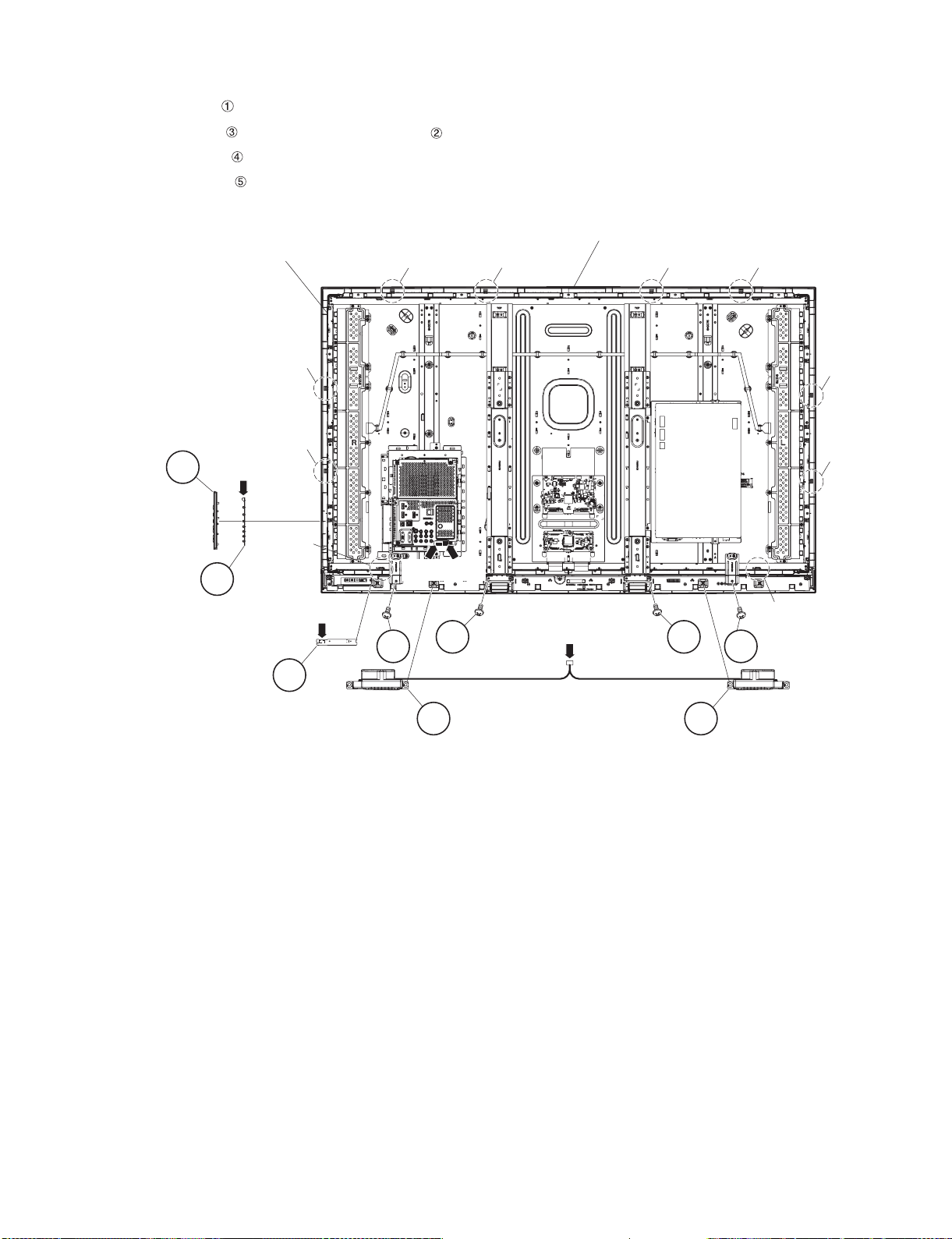
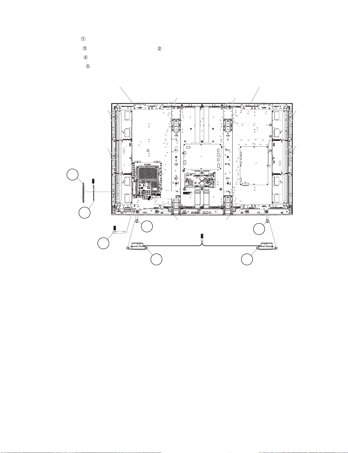
3. Removing of Connectors, Side Terminal Cover Ass’y, MAIN PWB Shield.
1. Remove the 3 lock screws , Side Terminal Cover Ass’y , 2 lock screws and 4 lock screws and detach the MAIN PWB Shield .
2. Disconnect the following connectors from the MAIN Unit. (LB1, PD, LP, LW, KM)
3. Disconnect the following connectors from the LCD Control Unit and FPGA Unit. (LW, PL, LP)
4. Disconnect the following connectors from the POWER Unit. (LA2, LA1, PD, PL)
LCD Panel Module Unit Ass'y
4
1
3
2Side Terminal
POWER UnitLCD Control Unit
Cover Ass'y
5MAIN PWB Shield
MAIN Unit
[KM]
MAIN Unit
[LB1]
[LP]
[PD]
[LW]
FPGA Unit
LCD Control Unit
[LW]
[LP]
[PL]
[PL]
[LA1]
[PD]
[PL]
FPGA Unit
POWER Unit
[LA2]
4 – 3
Page 17
LC-60E77UN/LC-65E77UM/LC-C6077UN/LC-C6577UM
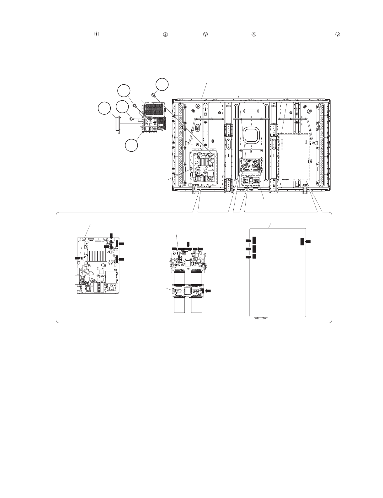
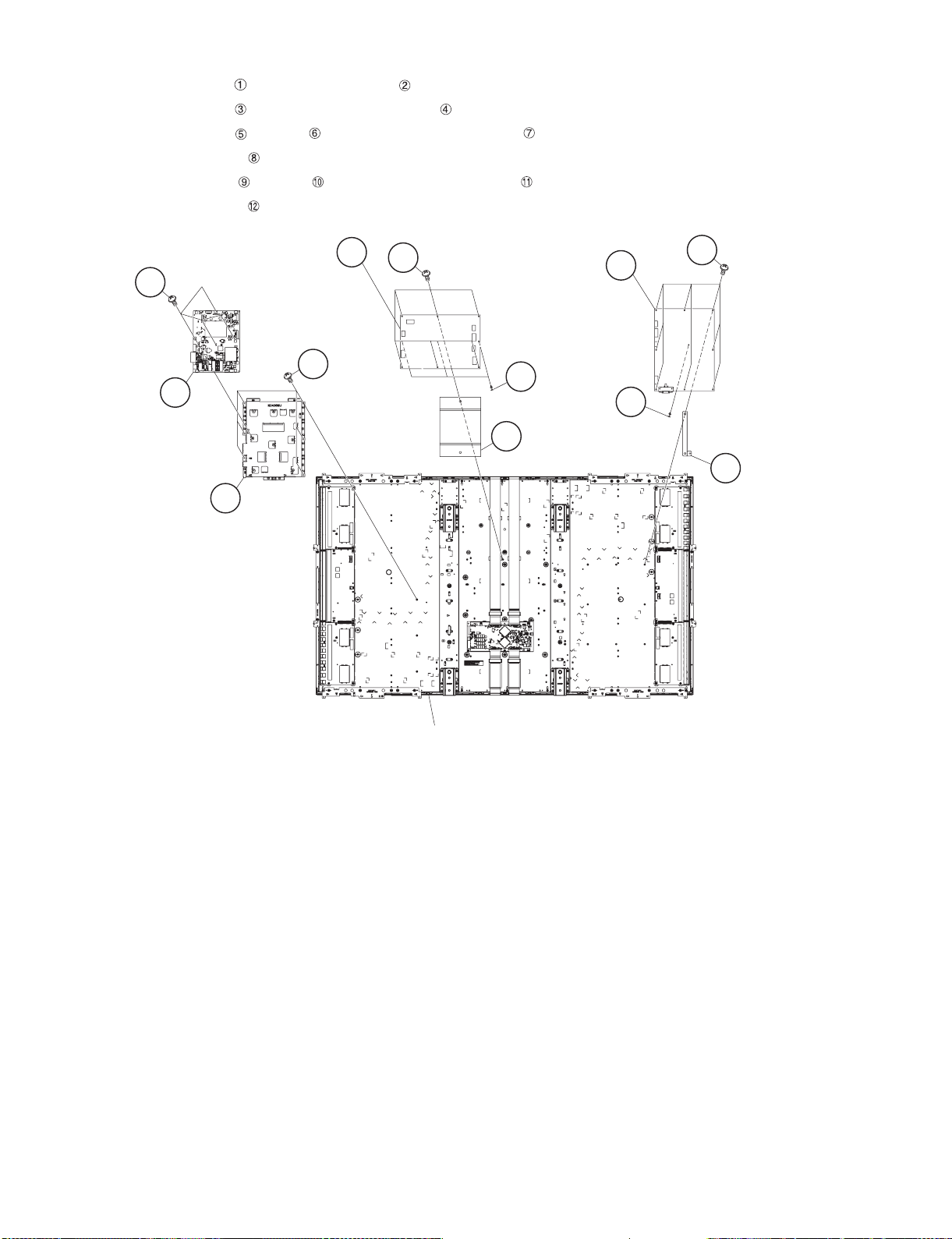
4. Removing of MAIN Unit, FPGA Unit, LCD Control Unit and POWER Unit.
1. Remove the 4 lock screws and detach the MAIN Unit .
2. Remove the 3 lock screws , 2 lock screws and 2 Panel Lug and detach the MAIN PWB Angle .
3. Remove the 4 lock screws and detach the FPGA Unit .
4. Remove the 4 lock screws and detach the LCD Control Unit .
5. Remove the 2 lock screws and 4 lock screws and detach the Control PWB Angle .
6. Remove the 8 lock screws and 1 hook and detach the POWER Unit .
7. Remove the 4 lock screws and detach the POWER PWB Angle
14
16POWER Unit
17
18POWER PWB Angle
15
LCD Panel Module Unit Ass'y
6MAIN PWB Angle
5 Panel Lug
2MAIN Unit
13
12
4
Control
PWB Angle
11
3
1
4
5 Panel Lug
10LCD Control Unit
9
Connecting
Cord
(FFC1)
8FPGA Unit
7
Connecting
Cord
(FFC2)
4 – 4
Page 18
LC-60E77UN/LC-65E77UM/LC-C6077UN/LC-C6577UM
5. Removing of VESA Angle and Support Angle.
1. Remove the 20 lock screws and detach the 4 VESA Angle .
2. Remove the 10 lock screws and detach the 2 Support Angle .
2VESA Angle
LCD Panel Module Unit Ass'y
1
1
4Support Angle
3 3
1 1
4 Support Angle
2 VESA Angle
4 – 5
Page 19
LC-60E77UN/LC-65E77UM/LC-C6077UN/LC-C6577UM
6. Removing of Bezel Ass’y, Micro Lens Sheet, Diffusion Plate, Reflector Sheet, INVERTER Unit-1/2 and BL
Chassis Ass’y.
1. Remove the 28 lock screws and detach the Bezel Ass’y .
2. Detach the Micro Lens Sheet .
3. Detach the Diffusion Plate .
4. Detach the 2 Lamp Holder , 44 Socket and 22 Lamp .
5. Detach the Reflector Sheet .
6. Remove the 12 lock screws and detach the INVERTER Cover-L .
7. Detach the INVERTER Unit-1 .
8. Remove the 12 lock screws and detach the INVERTER Cover-R .
9. Detach the INVERTER Unit-2 .
10.Detach the BL Chassis Ass’y .
12
INVERTER Cover-R
INVERTER Unit-2
14
13
9
INVERTER
Cover-L
10
6
5
Lamp Holder
Reflector Sheet
Socket
7
Lamp
8
5
6
Socket
Lamp Holder
15
BL Chassis Ass'y
4
11
INVERTER Unit-1
Diffusion Plate
1
3
Micro Lens Sheet
2
2
Bezel Ass'y
4 – 6
Page 20
LC-60E77UN/LC-65E77UM/LC-C6077UN/LC-C6577UM
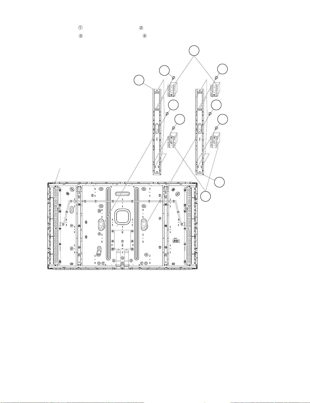
[2] REMOVING OF MAJOR PARTS (LC-65E77UM/LC-C6577UM)
1. Removing of Stand Unit and Rear Cabinet Ass’y.
1. Remove the 4 lock screws and detach the Stand Unit .
2. Detach the 5 Spacers .
3. Remove the 2 lock screws , 1 lock screw , 16 lock screws and detach the Rear Cabinet Ass’y.
33
6
4
3
5
1
2 Stand Unit
CAUTION: In the case of assembly, the new Spacer (PSPAGA386WJ00) can be stuck on a screw.
Rear Cabinet Ass'y
4 – 7
Page 21
LC-60E77UN/LC-65E77UM/LC-C6077UN/LC-C6577UM
2. Removing of Speaker-L/R, KEY Unit, R/C, LED Unit, Front Cabinet Ass’y.
1. Disconnect the following connectors from the MAIN Unit. (RA, SP)
2. Detach the Speaker-L/R .
3. Disconnect the KEY Unit from the KEY Button Cover Ass’y and disconnect the connection cord from the KM Connector.
4. Detach the R/C, LED Unit . (RA)
5. Remove the 2 lock screws and 8 Hooks and detach the Front Cabinet Ass’y
LCD Panel Module Unit Ass'y
Hook
Hook
2
[KM]
KEY Button
Cover Ass'y
3KEY Unit
[RA]
4R/C, LED Unit
[RA]
5
[SP]
Hook
[SP]
Front Cabinet Ass'y
Hook
Hook
Hook
HookHook
5
1 1Speaker-R Speaker-L
4 – 8
Page 22
LC-60E77UN/LC-65E77UM/LC-C6077UN/LC-C6577UM
3. Removing of Connectors, Side Terminal Cover Ass’y, MAIN PWB Shield.
1. Remove the 3 lock screws , Side Terminal Cover Ass’y , 2 lock screws and 4 lock screws and detach the MAIN PWB Shield .
2. Disconnect the following connectors from the MAIN Unit. (LB1, PD, LW, LP, KM)
3. Disconnect the following connectors from the MAIN POWER Unit. (LA, PP1, PP2, PP3, PQ, PL, PD)
4. Disconnect the following connectors from the SUB POWER Unit. (PP1, PP2, PP3, PQ)
5. Disconnect the following connectors from the LCD Control Unit. (LW, FR)
Cover Ass'y
[KM]
1
3
2Side Terminal
5MAIN PWB Shield
INVERTER-2 Unit
MAIN Unit
MAIN Unit
[LB1]
[LP]
[PD]
[LW]
4
LCD Panel Module Unit Ass'y
MAIN POWER Unit
[LC]
[LA2]
SUB POWER Unit
[LC]
[LA1]
INVERTER-5 Unit
[LB]
[LW]
[FR]
LCD Control Unit
MAIN POWER Unit
SUB POWER Unit
[LA]
[PL]
[PD]
[PP1]
[PP2]
[PP3]
[PP1]
[PP2]
[PP3]
[PQ]
[PQ]
4 – 9
Page 23
LC-60E77UN/LC-65E77UM/LC-C6077UN/LC-C6577UM
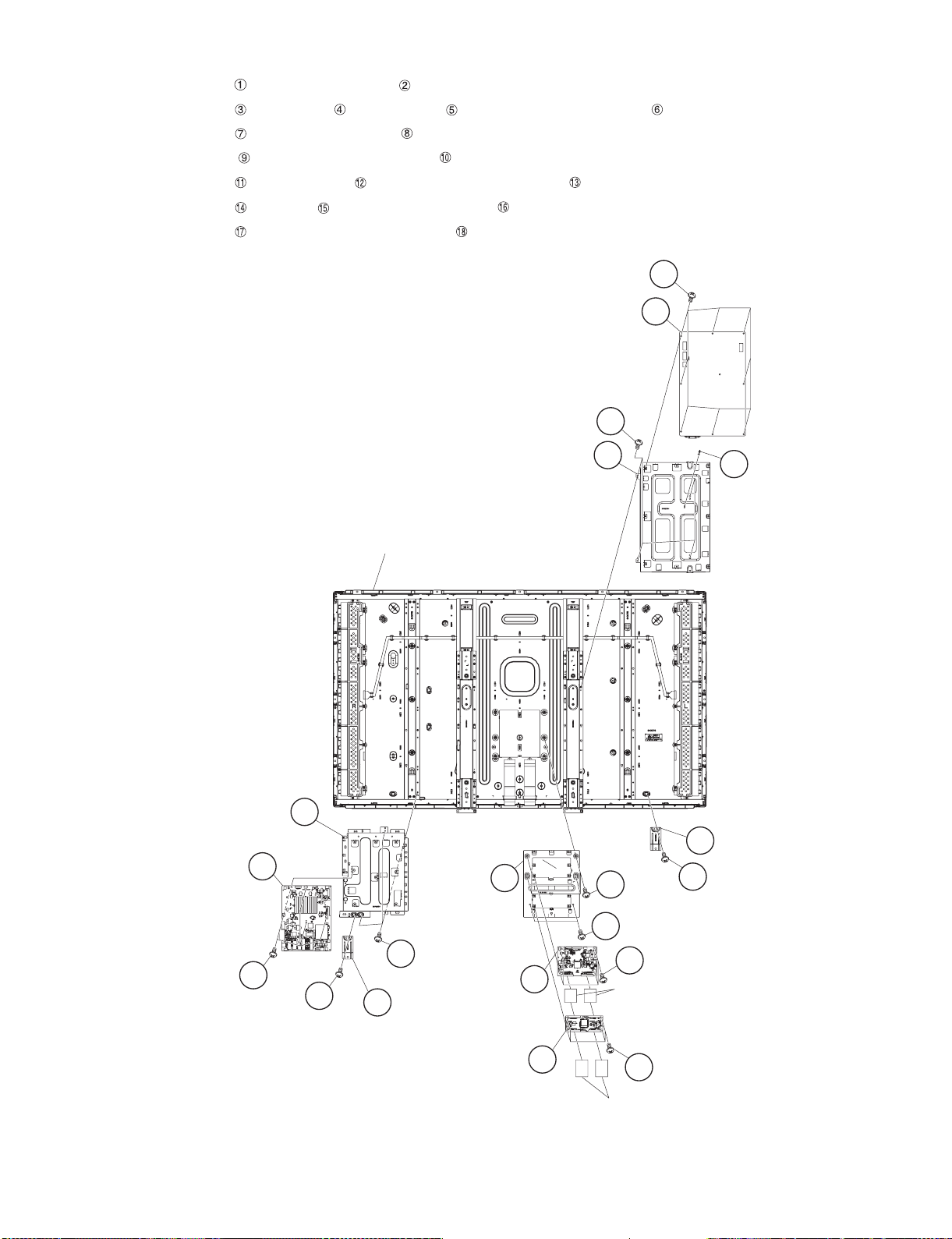
4. Removing of MAIN Unit, MAIN POWER Unit, SUB POWER Unit.
1. Remove the 4 lock screws and detach the MAIN Unit .
2. Remove the 6 lock screws and detach the MAIN PWB Angle .
3. Remove the 6 lock screws , 3 Spacer and detach the MAIN POWER Unit .
4. Detach the POWER2 Barrier .
5. Remove the 8 lock screws , 1 Spacer and detach the SUB POWER Unit .
6. Detach the POWER1 Barrier .
MAIN POWER Unit
1
2MAIN Unit
4MAIN PWB Angle
7
5
11SUB POWER Unit
9
3
6
10
8 POWER2 Barrier
12 POWER1 Barrier
LCD Panel Module Unit Ass'y
4 – 10
Page 24
LC-60E77UN/LC-65E77UM/LC-C6077UN/LC-C6577UM
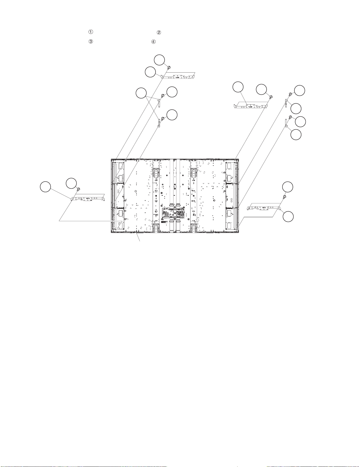
5. Removing of Corner Lug and Side Lug.
1. Remove the 8 lock screws and detach the 4 Corner Lug .
2. Remove the 4 lock screws and detach the 4 Side Lug .
1
2Corner Lug
Corner Lug
2
4Side Lug
3
2Corner Lug
1
3
Side Lug
4
3
3
4 Side Lug
1
1
2 Corner Lug
LCD Panel Module Unit Ass'y
4 – 11
Page 25
LC-60E77UN/LC-65E77UM/LC-C6077UN/LC-C6577UM
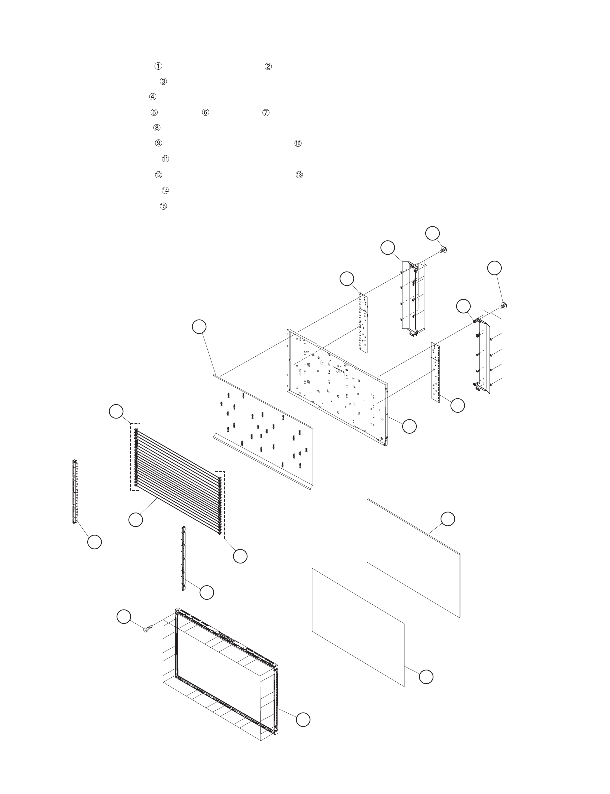
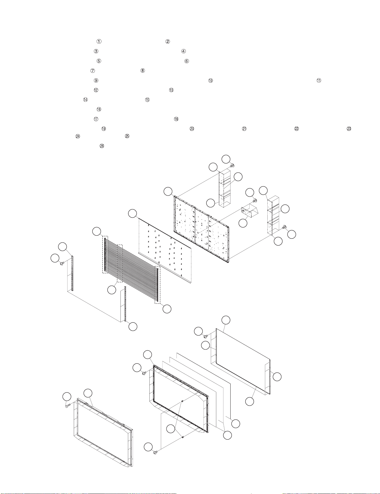
6. Removing of Bezel Ass’y, Panel Chassis Ass’y, Lens Sheet, Diffusion Plate, Sheet suppression Angle (L/R,
Top/Bottom), LCD Control Unit, INVERTER-1/2/3/4/5/6 and BL Chassis Ass’y.
1. Remove the 26 lock screws and detach the Bezel Ass’y .
2. Remove the 2 lock screws and detach the 2 Panel Guide Ass’y .
3. Remove the 26 lock screws and detach the Panel Chassis Ass’y .
4. Detach the 2 Lens Sheet and Diffusion Plate .
5. Remove the 8 lock screws and detach the 2 Sheet suppression Angle (L/R) and 2 Sheet Suppression Angle (Top/Bottom) .
6. Remove the 6 lock screws and detach the 2 Lamp Holder .
7. Detach the 72 Socket and detach the 36 Lamp .
8. Detach the Reflected Sheet .
9. Remove the 5 lock screws and detach the LCD Control Unit .
10.Remove the 29 lock screws and detach the INVERTER-1 Unit , INVERTER-2 Unit , INVERTER-3 Unit , INVERTER-4 Unit ,
INVERTER-5 Unit , INVERTER-6 Unit .
11.Detach the BL Chassis Ass’y .
19
25
23
INVERTER-5 Unit
24
17
18
LCD
Control Unit
INVERTER-3 Unit
INVERTER-1 Unit
20
21
22
INVERTER-2 Unit
19
12
13
Lamp Holder
Socket
Reflected Sheet
14
16
INVERTER-4 Unit
BL Chassis Ass'y
26
INVERTER-6
Unit
1
Lamp
Bezel Ass'y
2
15
13
Panel Chassis Ass'y
5
14
Socket
Lamp Holder
Sheet suppression Angle(L/R)
6
4
3
Sheet suppression Angle(Top/Bottom)
11
9
10
10
Sheet suppression
Angle(L/R)
11
Sheet suppression Angle(Top/Bottom)
8
Diffusion Plate
7
Lens Sheet
4 – 12
Page 26

LC-60E77UN/LC-65E77UM/LC-C6077UN/LC-C6577UM
LC60E77UN
CHAPTER 5. ADJUSTMENT
Service Manual
[1] ADJUSTMENT PROCEDURE
The adjustment values are set to the optimum conditions at the factory before shipping. If a value should become improper or an adjustment is
required due to part replacement, make an adjustment according to the following procedure.
1. After replacement of any PWB unit and/or IC for repair, please note the following.
• When replacing the following units, make sure to prepare the new units loaded with updated software.
MAIN Unit: DUNTKF282FM06 (LC-60E77UN)
DUNTKF282FM07 (LC-65E77UM)
DUNTKF282FM11 (LC-C6077UN)
DUNTKF282FM11 (LC-C6577UM)
• When replacing the LCD control PWB, perform the VCOM adjustment.
2. Upgrading of each microprocessor software
CAUTION: Never “POWER OFF” the unit when software upgrade is ongoing.
Otherwise the system may be damaged beyond recovery.
2.1. Software version upgrade
The model employs the following software.
• Main software (please use a software version after HLRCCxxx.USB.
• Monitor microprocessor software (please use a software version after HLRCCxxx.USB and HLNRMxxx.BIN.).
The main software, monitor microprocessor software can be upgraded by using a general-purpose USB Memory.
The followings are the procedures for upgrading, explained separately for the main software, monitor microprocessor software.
2.2. Main software version upgrade
2.2.1 Get ready before you start
• USB Memory of 128MB or higher capacity.
• PC running on Windows 98/98SE/ME/2000/XP operating system.
• USB Memory reader/writer or PC with a USB port.
• The file system of a USB memory is FAT (FAT32 supports).
• Use the USB memory without other functions (lock and memory reader...etc).
2.2.2 Preparations
To upgrade the main software, it is necessary to get ready the USB Memory for version upgrade before you start.
Follow the steps below and create the USB Memory for version upgrade.
1. Copy the file HLRCCxxx.USB. for version upgrade to the root directory (folder) of the USB Memory.
NOTE: In the USB Memory drive, do not store other folders or unrelated files, or more than one file for version upgrade.
Now the USB Memory for version upgrade is ready.
5 – 1
Page 27
LC-60E77UN/LC-65E77UM/LC-C6077UN/LC-C6577UM
2.2.3 How to upgrade the software
1. Unplug the AC cord.
2. Insert the USB Memory for version upgrade (prepared as above) into the service socket located Right side of Main Board terminals, under INPUT3
terminal.
3. Plug in the AC cord with power button pressed down after 5 seconds, unpress the power button.
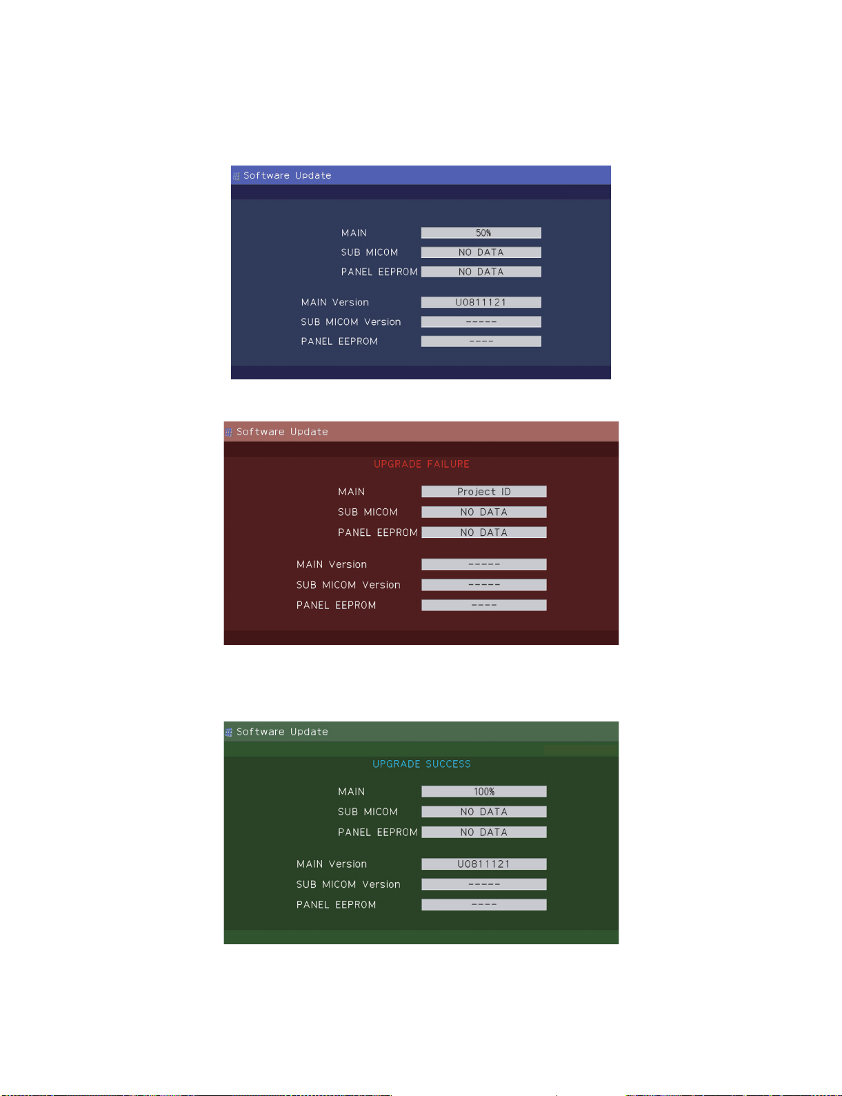
4. After the unit startup, the system upgrade screen as shown below appears within 20-40 seconds.
E77UN
5. Even a single failure in the process will trigger the upgrade failure screen.
E77UN
NOTE: In the event of a failure, repeat the upgrade process. If the process repeatedly fails, it is likely that the hardware need fixing.
6. Upon completion of the whole process, the upgrade success screen as shown below appears. You can check the new software version on this
screen. The version information appears after the upgrade is complete.
E77UN
7. Unplug the AC cord and remove the USB Memory for version upgrade.
8. Now the software version upgrade is complete.
NOTE: When you are done with the software version upgrade, start the set, go to the top page of the adjustment process screen and check the main
software version information.
5 – 2
Page 28
LC-60E77UN/LC-65E77UM/LC-C6077UN/LC-C6577UM
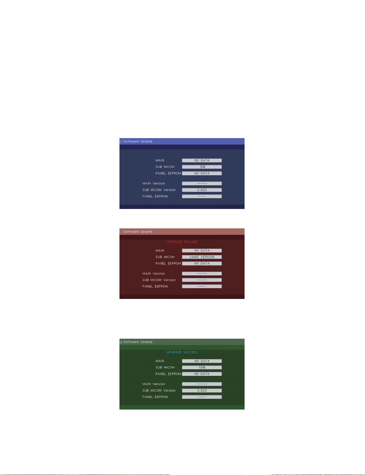
2.3. Monitor microprocessor software version upgrade
Create the USB memory for monitor microprocessor software version upgrade in the same manner as explained in the “Main software version
upgrade”.
Copy the file HLRCCxxx.USB and HLNRMxxx.BIN (named temporarily) for monitor microprocessor software version upgrade to the USB memory.
2.3.1 How to upgrade the software
1. Unplug the AC cord.
2. Insert the USB Memory for version upgrade (prepared as above) into the service socket located Right side of Main Board terminals, under INPUT3
terminal.
3. Plug in the AC cord with power button pressed down.
4. After 5 seconds, unpress the power button.
CAUTION: • The moment this operation is done, the upgrading of the monitor microprocessor software starts. While the upgrade is ongoing, never
5. After the unit startup, the upgrade starts. The power led will blink continuously. Also, an upgrade screen will be shown during a minor upgrade.
power off the unit. Otherwise the upgrade will fail and the system may be serious damaged beyond recovery (inability to start).
• After the monitor microprocessor software is upgraded, also perform the 'Industry Init'.
E77UN
6. If the upgrade fails, power led will stop blinking. Also, the upgrade failure screen will be shown if upgrade screen was shown at 5.
E77UN
NOTE: In the event of a transient failure, upgrade will be automatically retried up to three times. If the process repeatedly fails, hardware may be the
cause.
7. Up on completion of the whole process, power and OPC LED will blink alternately. Also, the upgrade success screen will be shown if upgrade
screen was shown at 5.
E77UN
8. Unplug the AC cord and remove the USB Memory for version upgrade.
9. Now the software version upgrade is complete.
NOTE: When you are done with the software version upgrade, start the set, go to the top page of the adjustment process screen and check the mon-
itor microprocessor software version information and panel size information.
5 – 3
Page 29
LC-60E77UN/LC-65E77UM/LC-C6077UN/LC-C6577UM
3. Entering and exiting the adjustment process mode
1) Before entering the adjustment process mode, the AV position RESET in the video adjustment menu.
2) While holding down the “VOL (–)” and “INPUT” keys at a time, plug in the AC cord of the main unit to turn on the power.
The letter “<K>” appears on the screen.
3) Next, hold down the “VOL (–)” and “CH ( )” keys at a time.
(The “VOL (–)” and “CH ( )” keys should be pressed and held until the display appears.)
Multiple lines of blue characters appearing on the display indicate that the unit is now in the adjustment process mode.
When you fail to enter the adjustment process mode (the display is the same as normal startup), retry the procedure.
4) To exit the adjustment process mode after the adjustment is done, unplug the AC cord from the outlet to make a forced shutdown. (When the
power was turned off with the remote controller, once unplug the AC cord and plug it again. In this case, wait 10 seconds or so before plugging.)
CAUTION: Use due care in handling the information described here lest your users should know how to enter the adjustment process mode. If the
4. Remote controller key operation and description of display in adjustment process mode
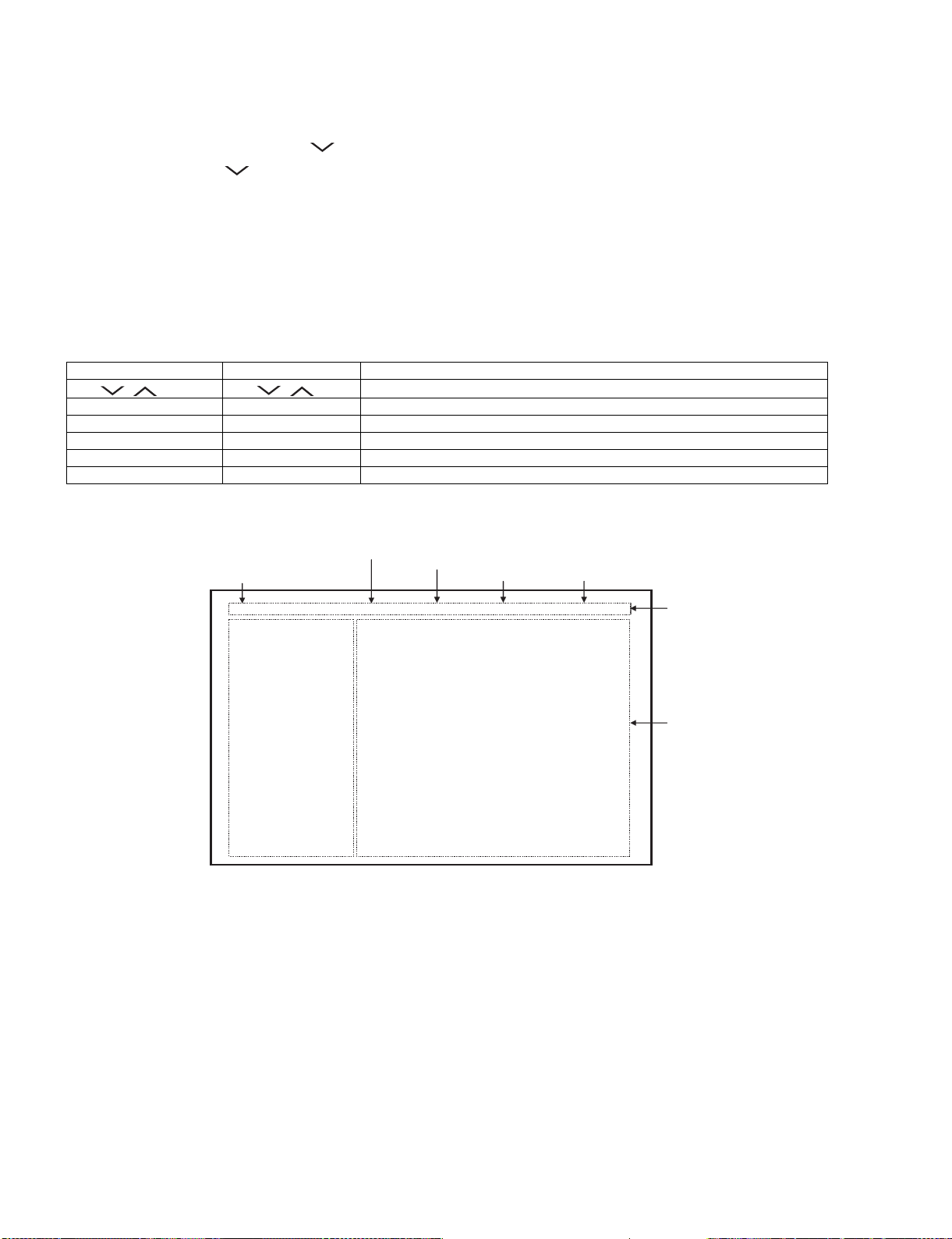
1) Key operation
Remote controller key Main unit key Function
CH ( / )
VOL (+/–) VOL (+/–) Changing a selected item setting (+1/ –1)
Cursor (UP/DOWN) ————— Turing a page (PREVIOUS/NEXT)
Cursor (LEFT/RIGHT) ————— Changing a selected line setting (+10/ –10)
INPUT ————— Input switching (toggle switching)
ENTER ————— Executing a function
settings are tampered in this mode, unrecoverable system damage may result.
CH ( / )
Moving an item (line) by one (UP/DOWN)
*Input mode is switched automatically when relevant adjustment is started so far as the necessary input signal is available.
2) Description of display
(1) Current page/
Total pages
1/40 INPUT5 AUTO USA 65_UNDER
MAIN Version
BOOT Version
Monitor/Monitor BOOT Version
LCD Con Version
LED TCON Version
EQ DATA CHECKSUM
TEMPERATURE
LAMP ERROR
MONITOR ERR CAUSE
NORMAL STANDBY CAUSE
ERROR STANDBY CAUSE
(2) Current selected input
(3) Current color system
1.09 (U 2009/07/07 1A)
HLNR 100
1.02/1.00
0900626000T0001
16
ROM
7B
0
0
0
1) 0 2) 0 3) 0
0H 0M 0H 0M 0H 0M
4) 0 5) 0
0H 0M 0H 0M
(4) Destination
(5) LCD Panel size/Speaker type
(6) Adjustment
process menu
header
(7) Parameters
5 – 4
Page 30

LC-60E77UN/LC-65E77UM/LC-C6077UN/LC-C6577UM
5. List of adjustment process mode menu
The character string in brackets [ ] will appear as a page title in the adjustment process menu header.
Page Line Item Description Remarks (adjustment detail, etc.)
1 1 MAIN Version Main software version
2BOOT Version
3 Monitor/Monitor BOOT Version Monitor and monitor boot software version
4 LCD Con Version LCD controller software version Versions are always ‘090626000T0001’.
5LED TCON Version
6 EQ DATA CHECKSUM Audio data checksum
7 TEMPERATURE Panel temperature
8 LAMP ERROR Number of termination due to lamp error
9 MONITOR ERR CAUSE
10 NORMAL STANDBY CAUSE Refer to *1 under the list for details
11 ERROR STANDBY CAUSE Refer to *2 under the list for details
2 1 INDUSTRY INIT Initialization to factory settings
2 INDUSTRY INIT(-Hotel)
3 PUBLIC MODE Public mode
4 Center Acutime Accumulated main operation time
5 RESET Reset
6 Backlight Acutime Accumulated monitor operation time
7 RESET Reset
8 LAMP ERROR RESET Reset LAMP ERROR
9 VIC XPOS X-coordinate setting for VIC READ
10 VIC YPOS Y-coordinate setting for VIC READ
11 VIC COLOR Collected color data setting for VIC READ
12 VIC SIGNAL TYPE Signal type setting for VIC READ
13 VIC READ Picture level acquisition function Level appears in green on the upper right
3 1 N358 ALL ADJ(INPUT1) CVBS and TUNER signal level adjustment
2 N358 ALL ADJ(INPUT3)
3 N358 MAIN ADJ(INPUT1) CVBS signal level adjustment
4 N358 MAIN ADJ(INPUT3)
5 TUNER DAC ADJ TUNER signal level adjustment
6 N358 CONTRAST A_GAIN
7 N358 CONTRAST D_GAIN
8 N358 CONTRAST OFFSET
9 TUNER CONTRAST A_GAIN
10 TUNER CONTRAST D_GAIN
11 TUNER CONTRAST OFFSET
4 1 TUNER VCHIP TEST(69ch) Tuning test and VCHIP test (69ch)
2 TUNER VCHIP TEST(7ch) Tuning test and VCHIP test (7ch)
3 TUNER VCHIP TEST(10ch) Tuning test and VCHIP test (10ch)
4 TUNER VCHIP TEST(15ch) Tuning test and VCHIP test (15ch)
5 INSPECT USB TERM
6 HDMI EDID WRITE
7 HDMI CEC TEST
5 1 COMP15K ADJ(INPUT1) Component 15K picture level adjustment (main)
2 COMP15K ADJ(INPUT2)
3 COMP15K Y A_GAIN
4 COMP15K Cb A_GAIN
5 COMP15K Cr A_GAIN
6 COMP15K Y OFFSET
7 COMP15K Cb OFFSET
8 COMP15K Cr OFFSET
6 1 COMP33K ADJ(INPUT1) Component 33K picture level adjustment (main)
2 COMP33K ADJ(INPUT2)
3 COMP33K Y A_GAIN
4 COMP33K Cb A_GAIN
5 COMP33K Cr A_GAIN
6 COMP33K Y OFFSET
7 COMP33K Cb OFFSET
8 COMP33K Cr OFFSET
5 – 5
Page 31

LC-60E77UN/LC-65E77UM/LC-C6077UN/LC-C6577UM
Page Line Item Description Remarks (adjustment detail, etc.)
7 1 ANALOG RGB ADJ Analog RGB picture level adjustment
2 R A_GAIN
3 G A_GAIN
4 B A_GAIN
5R OFFSET
6 G OFFSET
7 B OFFSET
8 1 VCOM ADJ VCOM adjustment value
9 1 DDR2 CHECK
2 BA[1:0]
3 ADDR[13:0]
4 DQ[15:0]
5 FRC ON/OFF
10 1 LEV1 Standard value 1 Adjustment gradation setting.
2 LEV2 Standard value 2
3 LEV3 Standard value 3
4 LEV4 Standard value 4
5 LEV5 Standard value 5
6 LEV6 Standard value 6
11 1 MG1R WB adjustment Point 1, R adjustment value Parameter for six-point adjustment
2 MG1G WB adjustment Point 1, G adjustment value
3 MG1B WB adjustment Point 1, B adjustment value
4 MG2R WB adjustment Point 2, R adjustment value
5 MG2G WB adjustment Point 2, G adjustment value
6 MG2B WB adjustment Point 2, B adjustment value
7 MG3R WB adjustment Point 3, R adjustment value
8 MG3G WB adjustment Point 3, G adjustment value
9 MG3B WB adjustment Point 3, B adjustment value
12 1 MG4R WB adjustment Point 4, R adjustment value Parameter for six-point adjustment
2 MG4G WB adjustment Point 4, G adjustment value
3 MG4B WB adjustment Point 4, B adjustment value
4 MG5R WB adjustment Point 5, R adjustment value
5 MG5G WB adjustment Point 5, G adjustment value
6 MG5B WB adjustment Point 5, B adjustment value
7 MG6R WB adjustment Point 6, R adjustment value
8 MG6G WB adjustment Point 6, G adjustment value
9 MG6B WB adjustment Point 6, B adjustment value
13 1 MODE SELECT
2 POS SELECT
3POS MIN
4POS MID1
5POS MID2
6POS MID3
7POS MID4
8POS MID5
9POS MID6
10 POS MAX
14 1 CD MIN
2 CD MID1
3 CD MID2
4 CD MID3
5 CD MID4
6 CD MID5
7 CD MID6
8 CD MAX
15 1 CALC
2 RESET
3VAL1
4VAL2
5VAL3
6VAL4
7VAL5
8VAL6
5 – 6
Page 32

LC-60E77UN/LC-65E77UM/LC-C6077UN/LC-C6577UM
Page Line Item Description Remarks (adjustment detail, etc.)
16 1 Audio Switch
2 Flat Mode
3 EEP STATUS INIT
4 Input Trim DTV
5 Input Trim ATV
6 Input Trim Digital
7 Input Trim Analog
8ATT1 Gain
9ATT2 Gain
10 ATT3 Gain
17 1 Auto Volume Threshold
2 Auto Volume Ratio
3 MBE Base Gain
4 MBE Output Gain
5 MBE BPF
6 MBE Force otct Mode
7 MBE Bass G Limit
8HPF FC
18 1 MVS Width
2 MVS Xtalk
3 MVS Clarity
4 MVS LR Gain
5 MVS Outout Gain
6 MVS Bass Gain
7 MVS FO
19 1 Bass CENTER ATT
2Bass Vol0 MAX
3Bass Vol60 MAX
4 Bass Vol60 CENTER
5Bass Vol0 MIN
6Bass Vol60 MIN
7 Treble CENTER ATT
8 Treble Vol0 MAX
9 Treble Vol60 MAX
10 Treble Vol60 CENTER
11 Treble Vol0 MIN
12 Treble Vol60 MIN
20 1 PEQ0 F0
2 PEQ0 Q
3 PEQ0 Gain
4 PEQ0 G Limit
5 PEQ1 F0
6 PEQ1 Q
7 PEQ1 Gain
8 PEQ1 G Limit
9 PEQ2 F0
10 PEQ2 Q
11 PEQ2 Gain
12 PEQ2 G Limit
21 1 PEQ3 F0
2 PEQ3 Q
3 PEQ3 Gain
4 PEQ3 G Limit
5 PEQ4 F0
6 PEQ4 Q
7 PEQ4 Gain
8 PEQ4 G Limit
9 PEQ5 F0
10 PEQ5 Q
11 PEQ5 Gain
12 PEQ5 G Limit
5 – 7
Page 33

LC-60E77UN/LC-65E77UM/LC-C6077UN/LC-C6577UM
Page Line Item Description Remarks (adjustment detail, etc.)
22 1 PEQ6 F0
2 PEQ6 Q
3 PEQ6 Gain
4 PEQ6 G Limit
5 PEQ7 F0
6 PEQ7 Q
7 PEQ7 Gain
8 PEQ7 G Limit
9 PEQ8 F0
10 PEQ8 Q
11 PEQ8 Gain
12 PEQ8 G Limit
23 1 AVC_L Fc
2 AVC_L Target Level
3 AVC_L Max Gain UP
4 AVC_L Attack Rate
5 AVC_L Release Rate
6 AVC_H Target Level
7AVC_H Max Galn UP
8 AVC_H Attack Rate
9 AVC_H Release Rate
24 1 Sub Vol. SP
2 Sub Vol. MON
3 Sub Vol. HP
4 Sub Vol. SW
5 Sub Vol. OPT
6 Clip Level SP
7 Clip Level MON
8 Clip Level HP
9 Clip Level SW
10 Clip Level OPT
25 1 PANNEL SELECT
2PWM
3PWM FREQ
4 PWM DUTY
5OSC FREQ
6 OSC DUTY
26 1 BRIGHTNESS DA0
2 BRIGHTNESS DA1
3 BRIGHTNESS DA2
4 BRIGHTNESS DA3
5 BRIGHTNESS DA4
6 BRIGHTNESS DA5
7 BRIGHTNESS DA6
8 BRIGHTNESS DA7
9 BRIGHTNESS DA8
10 BRIGHTNESS DA9
11 BRIGHTNESS DA10
12 BRIGHTNESS DA11
27 1 BRIGHTNESS DA12
2 BRIGHTNESS DA13
3 BRIGHTNESS DA14
4 BRIGHTNESS DA15
5 BRIGHTNESS DA16
6 BRIGHTNESS DA17
7 BRIGHTNESS DA18
8 BRIGHTNESS DA19
9 BRIGHTNESS DA20
10 BRIGHTNESS DA21
11 BRIGHTNESS DA22
5 – 8
Page 34

LC-60E77UN/LC-65E77UM/LC-C6077UN/LC-C6577UM
Page Line Item Description Remarks (adjustment detail, etc.)
28 1 BRIGHTNESS DA23
2 BRIGHTNESS DA24
3 BRIGHTNESS DA25
4 BRIGHTNESS DA26
5 BRIGHTNESS DA27
6 BRIGHTNESS DA28
7 BRIGHTNESS DA29
8 BRIGHTNESS DA30
9 BRIGHTNESS DA31
10 BRIGHTNESS DA32
29 1 OPC33 ADLEVEL 0
2 OPC33 ADLEVEL 1
3 OPC33 ADLEVEL 2
4 OPC33 ADLEVEL 3
5 OPC33 ADLEVEL 4
6 OPC33 ADLEVEL 5
7 OPC33 ADLEVEL 6
8 OPC33 ADLEVEL 7
9 OPC33 ADLEVEL 8
10 OPC33 ADLEVEL 9
11 OPC33 ADLEVEL 10
12 OPC33 ADLEVEL 11
30 1 OPC33 ADLEVEL 12
2 OPC33 ADLEVEL 13
3 OPC33 ADLEVEL 14
4 OPC33 ADLEVEL 15
5 OPC33 ADLEVEL 16
6 OPC33 ADLEVEL 17
7 OPC33 ADLEVEL 18
8 OPC33 ADLEVEL 19
9 OPC33 ADLEVEL 20
10 OPC33 ADLEVEL 21
11 OPC33 ADLEVEL 22
31 1 OPC33 ADLEVEL 23
2 OPC33 ADLEVEL 24
3 OPC33 ADLEVEL 25
4 OPC33 ADLEVEL 26
5 OPC33 ADLEVEL 27
6 OPC33 ADLEVEL 28
7 OPC33 ADLEVEL 29
8 OPC33 ADLEVEL 30
9 OPC33 ADLEVEL 31
32 1 V6 OS THERMO 1
2V6 OS THERMO 2
3V6 OS THERMO 3
4V6 OS THERMO 4
5V6 OS THERMO 5
6V6 OS THERMO 6
7V6 OS THERMO 7
33 1 V5 OS THERMO 1
2V5 OS THERMO 2
3V5 OS THERMO 3
4V5 OS THERMO 4
5V5 OS THERMO 5
6V5 OS THERMO 6
7V5 OS THERMO 7
34 1 BL TEMP1
2BL TEMP2
3BL TDUTY
35 1 MONITOR TIME OUT
2 MONITOR MAX TEMP
3 MONITOR ERROR CAUSE
RESET
5 – 9
Page 35

LC-60E77UN/LC-65E77UM/LC-C6077UN/LC-C6577UM
Page Line Item Description Remarks (adjustment detail, etc.)
36 1 LCD TEST PATTERN
2 LCD AGI TEST PATTERN
3 LCD EVA TEST PATTERN
4 YEL TEST PATTERN
5 TV TEST PATTERN 1
6 TV TEST PATTERN 2
37 1 REGISTER ADDRESS LOWER
2 READ/WRITE
3 SLAVE ADDRESS
4 REGISTER ADDRESS UPPER
5 WRITE DATA UPPER
6 WRITE DATA LOWER
7 READ DATA UPPER
8 READ DATA LOWER
38 1 KEY LOCK(1217)
2 KOUTEI AREA ALL CLEAR
3 A MODE AREA CLEAR
4 BACKUP AREA CLEAR
5 B MODE AREA CLEAR
6 EXECUTION
39 1 ERROR STANDBY CAUSE1
2 ERROR STANDBY CAUSE2
3 ERROR STANDBY CAUSE3
4 ERROR STANDBY CAUSE4
5 ERROR STANDBY CAUSE5
6 ERROR STANDBY CAUSE
RESET
40 1 EEP SAVE Writing setting values to EEPROM
2 EEP RECOVER Reading setting values from EEPROM
3MODL NAME
4 PANEL SIZE
5 SETTING FOR ADJ
6 PANEL LIMIT
7 PANEL RANGE LIMIT
8 SHORT CHECK MODE
9 SHORT CHECK CURRENT
10 CURRENT SW Must be Low. Don’t change
*1 Details of P1.9 (NORMAL STANDBY CAUSE)
2 No operation off in the cause of “no operation off”
3 No signal off in the cause of “no signal off”
4 PC power management mode 1 in the cause of “Standby mode MODE1”
5 PC power management mode 2 in the cause of “Standby mode MODE2”
6 Off timer in the cause of “SLEEP timer”
8 Command from RS232C in the cause of command by RS-232C
5 – 10
Page 36

LC-60E77UN/LC-65E77UM/LC-C6077UN/LC-C6577UM
H/2
V/2 V/2
*2 Details of P1.10 (ERROR STANDBY CAUSE)
11 Prolonged unspecified-signal input in PC mode in the cause of continuous “out of range”, PC input mode
17 Temperature error in the cause of abnormal temperature
1A Monitor trouble detected in the cause of abnormal monitor mode
22 LCD controller Rom error in the cause of software abnormality of LCD controller
6. Special features
* STANDBY CAUSE (Page 1/40)
Display of a cause (code) of the last standby
The cause of the last standby is recorded in EEPROM whenever possible.
Checking this code will be useful in finding a problem when you repair the troubled set.
* EEP SAVE (Page 40/40)
Storage of EEP adjustment value
* EEP RECOVER (Page 40/40)
Retrieval of EEP adjustment value from storage area
7. Microcomputer software writing
7.1. Main microcomputer/monitor microcomputer software writing (Main PWB: QPWBXF282WJZZ)
Adjustment item Adjustment conditions Adjustment procedure
1 Software writing
Main/Monitor microcomputer software
Checker process
File version check
USB memory check
1. Connect the given jig to SC9301 (TL9301-TL9309, TL9311-TL9316) using the
checker.
2. Connect the USB memory to J8001 (TL8003-8006) using the checker.
3. Apply the specified voltage to the main PWB and perform boot from the jig.
4.Send the software writing start command using RS232C.
5.Send the writing status check command and confirm the response of OK. Then
turn off the power.
CAUTION: When the USB memory is not inserted or reading error occurs, nothing
is written.
7.2. Model/inch discrimination writing (Main PWB: QPWBXF282WJZZ)
• When writing the sub microcomputer software, the model data is configured with the software from the USB memory mounted to the checker.
• Reference and setting change are enabled through the process menu (Page 40/40) and RS-232C communication.
8. Signal adjustment
8.1. LCD section adjustment 1 [LCD module adjustment]
Adjustment item Adjustment conditions Adjustment procedure
1 Opposite bias adjustment.
Left/Right
(LCD module adjustment
item)
Adjustment in the center
position of the panel
1. Enter the process mode using the process adjustment remote control.
2. Select [VCOM ADJ] using the Channel ↑, ↓ keys on the remote control.
3. Press the Enter key to check that the pattern for adjustment is displayed.
4. Make adjustment so that the flicker located in the center of the screen is minimized using the Volume +/- keys on the remote control.
5. If the status is optimized in step 4, press the Enter key to turn off the pattern.
CAUTION: * Make adjustment without ANT signal (since the active backlight
changes the brightness).
[Adjustment position]
5 – 11
Page 37

LC-60E77UN/LC-65E77UM/LC-C6077UN/LC-C6577UM
8.2. LCD section adjustment 2 [LCD module adjustment] (LC-65E77UM/LC-C6577UM Only)
Adjustment item Adjustment conditions Adjustment procedure
1 Vertical luminance differ-
ence adjustment
(LCD module adjustment
item)
Visual check
Adjustment in the middle of
the panel
8.3. Video Signal adjustment Procedure
8.3.1 Signal check
Before adjustment, check that the adjustment jig and signal source are set for Sharp LCD US.
Signal generator level adjustment check (Adjust to the standard value level.)
•Composite signal: 0.714Vp-p ± 0.02Vp-p (Pedestal to white level)
•15K component signal: Y level: 0.714Vp-p± 0.02Vp-p (Pedestal to white level)
PB/PR level: 0.7Vp-p ± 0.02Vp-p
•33K component signal: Y level: 0.7Vp-p ± 0.02Vp-p (Pedestal to white level)
PB/PR level: 0.7Vp-p ± 0.02Vp-p
•Analog RGB: RGB level: 0.7Vp-p ± 0.02Vp-p (Pedestal to white level)
1. Enter the process mode using the process adjustment remote control.
2. Select [LCD LUMA ADJ] using the Channel ↑/↓ keys on the remote control.
3. Press the Enter key to check that the pattern for adjustment is displayed.
4. Make adjustment so that the vertical luminance difference in the middle of the
screen is minimized using the Volume +/- keys on the remote control.
5. If the status is optimized in step 4, press the Enter key to turn off the pattern.
[Criterion]
No difference must be observable when visually checked.
CAUTION: The adjustment sequence is as follows:
Common Adjustment → Aging → Common adjustment → W/B adjustment (top) → Vertical luminance difference adjustment (bottom).
8.3.2 Process mode
Adjustment point Adjustment conditions Adjustment procedure
Process mode Enter the process adjustment mode using the process adjustment remote control.
8.3.3 Composite N358 signal/tuner adjustment
Adjustment point Adjustment conditions Adjustment procedure
1 Setting N358 signal
US-10ch
2 Automatic adjustment exe-
cution
•Send the N358 color bar (color saturation: 75%) signal to the Video 3 video input.
•Send the in-house signal (use US-10ch) to TUNER.
[Video input signal] [US-10CH]
75% Color saturation
100% white 100% white
Point the cursor to [ N358 ALL ADJ(INPUT3)] and press the [Enter] key.
The adjustment is complete when [ N358 ALL ADJ(INPUT3) OK] is displayed.
8.3.4 Component 15K signal adjustment
Adjustment point Adjustment conditions Adjustment procedure
1 Setting 480i signal •Send the 100% color bar signal to the Video 1 component input.
2 Automatic adjustment exe-
cution
100% Color saturation
480i
100% color bar
100% white 0% black
Point the cursor to [ COMP15K ADJ(INPUT1)] and press the [Enter] key.
The adjustment is complete when [ COMP15K ADJ(INPUT1) OK] is displayed.
5 – 12
Page 38

LC-60E77UN/LC-65E77UM/LC-C6077UN/LC-C6577UM
8.3.5 Component 33K signal adjustment
Adjustment point Adjustment conditions Adjustment procedure
1 Setting 1080i signal •Send the 100% color bar signal to the Video 1 component input.
2 Automatic adjustment exe-
cution
100% Color saturation
100% white 0% black
Point the cursor to [ COMP33K ADJ(INPUT1)] and press the [Enter] key.
The adjustment is complete when [ COMP33K ADJ(INPUT1) OK] is displayed.
1080i
100% color bar
8.3.6 Analog RGB signal adjustment
Adjustment point Adjustment conditions Adjustment procedure
1 Setting Analog RGB Signal: XGA •Send the 100% color bar signal to the Video 4 analog RGB input.
XGA (1024x768)
100% color bar
100% white 0% black
2 Automatic adjustment exe-
cution
Point the cursor to [ ANALOG RGB ADJ] and press the [Enter] key.
The adjustment is complete when [ ANALOG RGB ADJ OK] is displayed.
8.3.7 Tuner/V-CHIP adjustment
Adjustment point Adjustment conditions Adjustment procedure
1 Setting NTSC RF signal
US-7(AIR)ch
2 Automatic adjustment exe-
cution
•Send the NTSC signal to the RF antenna input.
Point the cursor to [ TUNER VCHIP TEST(*07ch)] and press the [Enter] key.
(* Adjust the selected channel to the in-house signal.)
The adjustment is OK when [ A-OK(***.**)/VM-OK] is displayed in Blue.
(NG when A-NG/VM-NG is displayed in Yellow or red.)
It is OK when the deviation from the center frequency is ±0.0625MHz or less.
5 – 13
Page 39

LC-60E77UN/LC-65E77UM/LC-C6077UN/LC-C6577UM
9. White balance adjustment
9.1. White balance adjustment (for LC-60E77UN/LC-C6077UN)
Adjustment point Adjustment conditions Adjustment procedure
1 Setting (For details about the adjustment procedure, refer to “Kameyama Model Integrated Mon-
2 Automatic adjust-
ment execution
[Command]
Process mode
KRSW0001
KKT10037
Setting
KYOF0000
OSDS0001
SBSL0016
Multi-point adjustment
mode
MSET0001
Point 6
WBI60928
MG6G****
MG6B****
MG6R****
Point 5
WBI50808
MG5G****
MG5B****
MG5R****
itor WB Adjustment Specification V1.4”.)
1) Set the set to the following conditions.
AV MODE: [DYNAMIC]
Backlight: +16
Active Contrast: OFF
Aging Time: Min. 60 minutes
2) Connect the set with the white balance adjustment jig.
[Adjustment procedure]
1) Transmit the “Monitor adjustment process” code using the remote control.
2) Set the point 6 to the specified gradation, specify the strongest color as the fixed
color, and adjust the RGB so that it becomes the standard value through negative
adjustment.
3) Set the point 5 to the specified gradation, set the G correction value (3232 x G value
of point 6/3712) (fractions rounded off), and adjust the RB so that it becomes the
standard value.
4) Set the point 4 to the specified gradation, set the G correction value (2784 x G value
of point 6/3712) (fractions rounded off), and adjust the RB so that it becomes the
standard value.
5) Set the point 3 to the specified gradation, set the G correction value (1920 x G value
of point 6/3712) (fractions rounded off), and adjust the RB so that it becomes the
standard value.
6) Set the point 2 to the specified gradation, set the G correction value (944 x G value of
point 6/3712) (fractions rounded off), and adjust the RB pattern so that it becomes the
standard value.
7) Set the point 1 to the specified gradation, set the G correction value (736 x G value of
point 6/3712) (fractions rounded off), and adjust the RB so that it becomes the standard value.
8) Write the adjustment value by the MSET0003 command and turn off the AC power.
* RGB initial value of point 6: Set gradation 3712
* RGB initial value of points 1 to 5: G correction value of each point
[Adjustment value]
* According to the “Standard settings” submitted by the Technical Department
[Adjustment standard value]
Measuring instrument: [Minolta CA-210] Technical measuring instrument
Point 4 Level Reference value Adjustment spec Inspection spec
WBI40696
MG4G**** y=0.277
MG4B****
MG4R**** y=0.277
Point 3 y=0.277
WBI30480
MG3G**** y=0.277
MG3B****
MG3R**** y=0.277
Point 2
WBI20236
MG2G****
MG2B****
MG2R****
Point 1
WBI10184
MG1G****
MG1B****
MG1R****
Writing
MSET0003
Point 6 928
Point 5 808
Point 4 696
Point 3 480
Point 2 236
Point 1 184
Remarks Setting conditions when performing inspection
X=0.272
X=0.272
X=0.272
X=0.272
X=0.272
X=0.272
y=0.277
AV MODE: [DYNAMIC] (Reset)
Monochro: ON
Active Controst: OFF
Aging Time: Min. 60 minutes
±0.0010 ±0.0020
±0.0010 ±0.0020
±0.0015 ±0.0030
±0.0020 ±0.0040
±0.0030 ±
±0.0045 ±0.0090
0.0060
5 – 14
Page 40

LC-60E77UN/LC-65E77UM/LC-C6077UN/LC-C6577UM
9.2. White balance adjustment (for LC-65E77UM/LC-C6577UM)
Adjustment point Adjustment conditions Adjustment procedure
1 Setting (For details about the adjustment procedure, refer to “Kameyama Model Integrated Mon-
itor WB Adjustment Specification V1.4”.)
1) Set the set to the following conditions.
AV MODE: [DYNAMIC]
Backlight: +16
Active Contrast: OFF
Aging Time: Min. 60 minutes
2) Connect the set with the white balance adjustment jig.
2 Automatic adjust-
ment execution
[Command]
Process mode
KRSW0001
KKT10037
Setting
KYOF0000
OSDS0001
SBSL0016
Multi-point adjustment
mode
MSET0001
Point 6
WBI60928
MG6G****
MG6B****
MG6R****
Point 5
WBI50784
MG5G****
MG5B****
MG5R****
[Adjustment procedure]
1) Transmit the “Monitor adjustment process” code using the remote control.
2) Set the point 6 to the specified gradation, specify the strongest color as the fixed
color, and adjust the RGB so that it becomes the standard value through negative
adjustment.
3) Set the point 5 to the specified gradation, set the G correction value (3136 x G value
of point 6/3712) (fractions rounded off), and adjust the RB so that it becomes the
standard value.
4) Set the point 4 to the specified gradation, set the G correction value (2320 x G value
of point 6/3712) (fractions rounded off), and adjust the RB so that it becomes the
standard value.
5) Set the point 3 to the specified gradation, set the G correction value (1680 x G value
of point 6/3712) (fractions rounded off), and adjust the RB so that it becomes the
standard value.
6) Set the point 2 to the specified gradation, set the G correction value (1136 x G value
of point 6/3712) (fractions rounded off), and adjust the RB pattern so that it becomes
the standard value.
7) Set the point 1 to the specified gradation, set the G correction value (736 x G value of
point 6/3712) (fractions rounded off), and adjust the RB so that it becomes the standard value.
8) Write the adjustment value by the MSET0003 command and turn off the AC power.
* RGB initial value of point 6: Set gradation 3712
* RGB initial value of points 1 to 5: G correction value of each point
[Adjustment value]
* According to the “Standard settings” submitted by the Technical Department
[Adjustment standard value]
Measuring instrument: [Minolta CA-210] Technical measuring instrument
Point 4 Level Reference value Adjustment spec Inspection spec
WBI40580
MG4G**** y=0.277
MG4B****
MG4R**** y=0.277
Point 3 y=0.277
WBI30420
MG3G**** y=0.277
MG3B****
MG3R**** y=0.277
Point 2
WBI20284
MG2G****
MG2B****
MG2R****
Point 1
WBI10184
MG1G****
MG1B****
MG1R****
Writing
MSET0003
Point 6 928
Point 5 784
Point 4 580
Point 3 420
Point 2 284
Point 1 184
Remarks Setting conditions when performing inspection
X=0.272
X=0.272
X=0.272
X=0.272
X=0.272
X=0.272
y=0.277
AV MODE: [DYNAMIC] (Reset)
Monochro: ON
Active Controst: OFF
Aging Time: Min. 60 minutes
±0.0010 ±0.0020
±0.0010 ±0.0020
±0.0015 ±0.0030
±0.0020 ±0.0040
±0.0030 ±0.0060
±0.0040 ±0.0080
5 – 15
Page 41

LC-60E77UN/LC-65E77UM/LC-C6077UN/LC-C6577UM
10. Key writing
10.1. EDID writing (Main PWB: QPWBXF282WJZZ HDMI • RBG Input Terminal)
Adjustment point Adjustment conditions Adjustment procedure
1 HDMI EDID writing
(Main PWB)
2 Analog RGB EDID writing
(Main PWB)
10.2. MAC address writing (Main PWB: QPWBXF282WJZZ)
1. Write the MAC key data into IC8453 mounted on the MAIN PWB via RS232C.
2. The data must be written before making the inspection using the checker.
Inspection mode
File version check
Inspection mode
File version check
1) Enter the process mode.
2) Point the cursor to [EDID WRITE ENT] and press the [ENT] key.
The writing is complete when [ENT WRITE OK] is displayed.
(If not written, HDMI does not function.)
CAUTION: Perform the data writing after setting the model discrimi-
nation. The data based on the model discrimination information is recorded in EEPROM.
1) Write the EDID data for analog RGB into IC1809 mounted on the
main PWB.
TL1821 ••• I2C clock, TL1823 ••• I2C data
TL1824 ••• 5V, TL1822 ••• GND
TL1848 ••• Write protection (H: WP, L: write enable)
2) Perform the data writing before making inspection using the
checker.
5 – 16
Page 42

LC-60E77UN/LC-65E77UM/LC-C6077UN/LC-C6577UM
11. Factory setting
After completing the factory setting, pull out the AC cord to complete the setting.
CAUTION: Do not turn on the power after completing the factory setting. If the power is turned on, configure the factory setting again.
Adjustment point Adjustment conditions Adjustment procedure
1 Factory setting Complete the setting by
pulling out the AC cord.
12. Writing the inch and model name onto EEPROM
Writing method
1. Pull out the AC cord.
2. Copy the application for writing inch/model name (HLNRMA01.USB) and model/inch file (60E77.MDL) to the USB memory.
3. Hold down the power button and insert the AC cord.
4. Release the power button after 5 seconds.
5. Update starts.
•Point the cursor to [INDUSTRY INIT (+Cause)], set to “ON” using [+]/[-] of the [VOL] key,
and press the [ENT] key.
The version confirmation screen appears on the green screen. It is completed when [SUCCESS] is displayed at the top.
(If error occurs, [ERROR] is displayed on the red screen.)
•Turn off the AC power.
The following items are initialized when configuring the factory setting.
1) User setting values
2) Channel data (broadcasting frequency, etc.)
3) Password setting value
4) Operating time
5) Standby Cause (Monitor, Main)
6) Auto installation flag
7) V-CHIP block setting value
60E77
The inch and model name are displayed.
UPGRADE SUCCESS
6. Pull out the AC cord.
Model/inch file
• 60E77.MDL
• 65E77.MDL
• C6077.MDL
• C6577.MDL
NOTE: When replacing the main PWB, make sure to perform the writing the inch and model name onto EEPROM
5 – 17
Page 43

LC-60E77UN/LC-65E77UM/LC-C6077UN/LC-C6577UM
[2] PUBLIC MODE SETTING PROCEDURE
1. How to start Public Mode
• There are the following two ways to get the public mode setup screen displayed.
In the adjustment process mode, turn on “PUBLIC MODE”. Also press the “CH ( )” and “VOL (+)” keys on the set at once and turn on the
power.
1) Press the “INPUT” and “VOL (+)” keys on the set at once and turn on the power.
2) Get the password input screen displayed.
Procedure
˴The input starts with the leftmost digit.
˴Use the numeric keys [1] thru [9] and [0] keys on the remote controller.
˴The other keys are not acceptable.
˴With a numeric-key input, "_" will change to "˴".
˴The input position will move one digit to the right.
˴With all the 3 digits entered, the password will be verified.
3) The 3-digit password is now verified.
The password [0] [2] [7] provides for the public mode screen. (This screen comes on with whatever adjustment process settings.)
With any other passwords, the screen changes to the normal mode.
2. How to exit Public Mode
There are the following ways to quit the public mode setup screen.
• Turn off “PUBLIC MODE” in the adjustment process mode. ( ) ← This way alone is not for quitting the setup screen, but for quitting the mode itself.
• Turn off the power with the “POWER” key. ( )
• Select “EXECUTE”. ( )
... “PUBLIC MODE” stays on in the adjustment process mode.
... The settings will be back to the factory ones.
3. Public Mode Setting Values
• With the factory settings made, the public mode settings get initialized. (The adjustment process remains intact.)
5 – 18
Page 44

LC-60E77UN/LC-65E77UM/LC-C6077UN/LC-C6577UM
4. Public Mode Menu
The guidance is not displayed on screen.
Setup procedure
• To move the cursor up and down, use the “cursor UP/DOWN” key (remote controller) and “CH ( )/( )” key (remote controller and set).
• To change the settings, use the “cursor RIGHT/LEFT” key (remote controller) and “VOL (+)/(–)” key (remote controller and set).
• To save new settings, keep the cursor at “EXECUTE” and use “ENTER” key (remote controller and set).
PUBLIC MODE
POWER ON FIXED [VARIABLE ]
MAXIMUM VOLUME [ 60 ]
VOLUME FIXED [VARIABLE ]
VOLUME FIXED LEVEL [ 20 ]
RC BUTTON [RESPOND ]
PANEL BUTTON [RESPOND ]
MENU BUTTON [RESPOND ]
AV POSITION FIXED [VARIABLE ]
ON SCREEN DISPLAY [YES ]
INPUT MODE START [NORMAL ]
INPUT MODE FIXED [VARIABLE ]
LOUD SPEAKER [ON ]
RC_PATH_THROUGH [OFF ]
232C POWON [DISABLE ]
PUBLIC MODE [OFF ]
RESET
EXECUTE
5 – 19
Page 45

LC-60E77UN/LC-65E77UM/LC-C6077UN/LC-C6577UM
5. On Setting Items
* “EZ-SETUP” discussed below indicates “EZ-SETUP after the first power-on”.
1) POWER ON FIXED
Selection Selection between “Variable” and “Fixed” (loop provided)
Default – (Variable)
Explanation In “Fixed” setting, the power-off by the power key of the unit is invalidated and the image is kept being received. The power can
Limit in Setting Refer to the “Power-On Fixed” sheet.
Exception None
Remarks • In “Variable” setting, the power operation is in wait for 1 sec. and then turned off when the main power switch is off.
2) MAXIMUM VOLUME
Selection Adjustment from 0 to 60 (no loop)
Default 60
Explanation Sound volume can not be adjusted higher than the preset value.
Limit in Setting • When the sound volume is set lower than 59, only figures are displayed and the sound volume bar is not displayed.
Exception
Remarks • When the sound volume is set higher than the MAX setting by the adjusting process, the sound volume control operation is
3) VOLUME FIXED
be turned off by stopping the power supply from AC.
• The maximum sound volume for ON-timer (Wake up timer) is limited also to the preset value.
prohibited for turn-up and the sound volume should be turned down to MAX in this state.
Selection Selection between “Variable”, “Fixed”, “ACON (AC CTRL)” and “AC/RCON (AC/RC CTRL)” (loop provided)
Default Variable
Explanation • FIXED: Fixed at the level adjusted for a fixed volume.
• AC CTRL: Start-up at the level specified for a fixed volume at ACON.
• AC/RC CTRL: Start-up at the level specified for a fixed volume at start.
Limit in Setting • The sound volume for the ON-timer (Wake up timer) is fixed also without display of menu. Besides, the setting is made
impossible. (Basically, the menu is not displayed.)
• The following keys become invalid:
• Sound volume Up/Down (VOL +/–) [for both remote control and the unit]
• Mute (MUTE)
Exception • In the item “VOLUME” of adjustment process, the sound volume can be set freely irrespective of this setting.
Remarks • As for sound volume fixing and sound volume MAX level, the sound volume fixing has priority.
• Once the sound volume has been changed by adjustment process, it should be set back to the sound volume preset by
sound volume fixing level when the adjustment process ends.
4) VOLUME FIXED LEVEL
Selection Adjustment from 1 to 60 (no loop)
Default 20
Explanation The sound volume to be fixed by “Volume fixed” is determined.
Limit in Setting None
Exception None
Remarks Setting is valid only when “Volume fixed” is selected for “fixed”.
5) RC BUTTON
Selection Selection between “Respond”, “No Respond” and “Limited” (loop provided)
Default Respond
Explanation Making the remote controller settings.
• At the “No Respond” setting, the remote controller keys are disabled. Its power key (reception/standby key) is disabled too.
• At the “Limited” setting, some channel-related keys alone are operative. All the other remote controller keys (power, volume
/ , channel / , light control (brightness sensor), broadcast select) are inoperative.
Limit in Setting
Exception • Adjustment process, inspection process and hotel only keys are valid irrespective of setting.
Remarks
In “No respond” setting, all the keys (including the power key) are not accepted.
•
All the keys can be used in adjustment process, inspection mode and hotel menu irrespective of setting.
5 – 20
Page 46

LC-60E77UN/LC-65E77UM/LC-C6077UN/LC-C6577UM
6) PANEL BUTTON
Selection Selection between “Respond” and “No respond” (loop provided)
Default Respond
Explanation All the operations by keys (except the power key) of the unit can be invalidated.
Limit in Setting
Exception • Adjustment process, inspection mode and hotel menu mode can be started irrespective of setting.
• All the keys can be used in adjustment process, inspection mode and hotel menu irrespective of setting.
Remarks
7) MENU BUTTON
Selection Selection between “Respond” and “No respond” (loop provided)
Default Respond
Explanation In “No respond” setting, the menu operation by the menu key of the remote control and the menu key of the unit are invali-
dated.
Limit in Setting
Exception • Adjustment process, inspection mode and hotel menu mode can be started irrespective of setting.
• All the keys can be used in adjustment process, inspection mode and hotel menu irrespective of setting.
Remarks
8) ON SCREEN DISPLAY
Selection Selection between “Yes”, “No” (loop provided)
Default Yes
Explanation • At the “No” setting, the following items are not displayed on screen: register, setting, adjustment menu, channel call and vol-
ume bar.
On the wide-screen models, an input selection is immediately made because the menu is not displayed.
• At the “Limited” setting, some items cannot be displayed on screen.
On the Japan-destined models, the channel call “Message” alone cannot be displayed. (This is because the channel call message may be confused with a message being sent from the hotel.)
On the North America-destined models, the OSD works the same as at the “No” setting.
Limit in Setting • Keys falling under any of the following items become invalid.
Appearance of screen changes and the sound changes.
Personal functions which are hard to restore.
Screen display, menu, OFF-timer, ON-timer, AV MODE, screen size switching, clock setting, treble emphasis, AUDIO ONLY,
sound changeover, LANGUAGE, CLOSED CAPTION
Others • Simple input switching is generated. Those which are restored soon after leaving as they are and may be requested for
change by customer are not prohibited.
Brightness sensor (BACKLIGHT) and PIC. FLIP
Exception • Such a caution which is displayed independently is displayed as it is.
Non-responding signal caution
Remarks • When CC has already been ON, CLOSED CAPTION is displayed.
9) INPUT MODE START
Selection
Default Normal
Explanation In power-ON, the input source to be started or channel can be set.
About options • All the input sources in the model are made selectable.
Limit in Setting • The display of channel setting menu and the channel setting operation are prohibited.
Exception
Remarks • In setting at “Normal”, the setting of “Input mode fixed” is changed to “Variable” and selection should be prohibited.
Selection between “Normal”, “Air ( )”, “INPUT 1/2/3”, “PC”, “HDMI 1/2/3/4/5”, “DVI” (loop provided)
(In standard mode, the operation follows the last memory.)
• In TV mode, the channel to be set follows the last memory and the content of the last memory is included in the notation by
options. Ex.) Air (2), Cable (98.1) etc.
5 – 21
Page 47

LC-60E77UN/LC-65E77UM/LC-C6077UN/LC-C6577UM
10)INPUT MODE FIXED
Selection Selection between “Variable”, “Fixed”, “ACON (AC CTRL)” and “AC/RCON (AC/RC CTRL)” (loop provided)
Default – (Variable)
Explanation • At the “Fixed” setting, the TV set gets started with the settings of “Input mode start”, and then any other channels and inputs
are not accepted.
• At the “ACON (AC CTRL)” setting, the TV set gets started with the settings of “Input mode start” under AC control.
• At the “AC/RCON (AC/RC CTRL)” setting, the TV set gets started with the settings of “Input mode start” under either control.
Limit in Setting • With the execution of hotel mode, the input source is forced to change to that set by “Input mode start” and the channel
Exception None
Remarks • In the following case, setting is cancelled and mode is changed to “Variable”.
11)RC_PATH_THROUGH
Selection Selection between “OFF”, “ON: TV RCE” and “ON: TV RCD” (loop provided)
Default OFF
Explanation Function to feed the remote controller-received signal to Pin 9 (open) on the RS232C.
Limit in Setting None
Exception None
Remarks None
switching and input switching are prohibited thereafter.
• ON-timer's (Wake-up timer) channel items are not displayed or the operation is prohibited. (Basically, they are not displayed.)
• The following keys are invalidated.
CH / , direct tuning button, FLASHBACK, input
However, the keys (input switching and CH / keys) of the unit for menu operation remain valid.
When the setting of “Input mode start” is set to “Normal”.
12)AV POSITION FIXED
Selection Selection between “Variable” and “Fixed” (loop provided)
Default Variable
Explanation In case of “Fixed” setting,
– Menu “Picture” and “Audio” setting can't be changed like “Dynamic (Fixed)”.
– When “AV Mode” key is pressed, TV just displays current AV Mode (cannot be changed.).
Limit in Setting None
Exception None
Remarks • When receiving with AV Position key, OPC, Dolby key and other direct audio select keys, the current display stays on and no
setting can be changed.
• Even by initializing personal information, the hotel-mode settings are kept intact. In this way, the AV positions, video and
audio adjustment settings are not initialized.
13)LOUD SPEAKER (ON/OFF)
Selection Selection between “ON” and “OFF” (loop provided)
Default ON
Explanation If “OFF” is selected, TV stops Speaker output even without Headphone connected.
Limit in Setting None
Exception None
Remarks • Press the volume UP/DOWN key, and the mute icon appears for 4 seconds.
• The mute key and audio-related keys are displayed with caution.
• Usually, the headphones and monitor audio outputs can be adjustable.
14)232C POWON
Selection Selection between “Disable” and “Enable” (loop provided)
Default Disable
Explanation In the standby mode, the power-on by the 232C command is enabled or disabled.
Limit in Setting None
Exception None
Remarks None
5 – 22
Page 48

LC-60E77UN/LC-65E77UM/LC-C6077UN/LC-C6577UM
15)PUBLIC MODE (ON/OFF)
Selection Selection between “ON” and “OFF” (loop provided)
Default OFF
Explanation In case of “ON”, public mode settings are effected.
Limit in Setting None
Exception None
Remarks The public-mode settings are operable only when this item is set at ON.
5 – 23
Page 49

LC-60E77UN/LC-65E77UM/LC-C6077UN/LC-C6577UM
LC60E77UN
CHAPTER 6. TROUBLESHOOTING TABLE
Service Manual
[1] TROUBLESHOOTING TABLE
No video (1)
COMPOSITE: No external input video [INPUT-1] COMPOSITE: No external input video [INPUT-3]
Is INPUT-1 selected on the input select menu screen? Is INPUT-3 selected on the input select menu screen?
NO
Select INPUT-1 on the input select menu
screen for the right input signal.
Does the INPUT-1 V1_PLUG detection function?
Check the line between pin (7) of input terminal
(J507) and pin (AJ1) of IC8001 (CPU).
YES
Is there the COMPOSITE signal input at pin (AE28) of IC8001
(CPU)?
NO
Check the line between pin (8) of J507 and pin
(AE28) of IC8001.
YES
Are the LVDS signal outputs at the LVDS 1st channel and 2nd channel of IC8001?
LVDS_TX_0_DATA0_P/N (C14/D14), LVDS_TX_0_DATA1_P/N (C15/D15),
LVDS_TX_0_DATA2_P/N (C16/D16), LVDS_TX_0_DATA3_P/N (C18/D18),
LVDS_TX_0_DATA4_P/N (C19/D19), LVDS_TX_0_CLK_P/N (C17/D17),
LVDS_TX_1_DATA0_P/N (A14/B14), LVDS_TX_1_DATA1_P/N (A15/B15),
LVDS_TX_1_DATA2_P/N (A16/B16), LVDS_TX_1_DATA3_P/N (A18/B18),
LVDS_TX_1_DATA4_P/N (A19/B19), LVDS_TX_1_CLK_P/N (A17/B17).
YES
Check the panel module.
Is there the COMPOSITE signal input at pin (AE29) of IC8001 (CPU)?
NO
Select INPUT-3 on the input select menu screen
for the right input signal.
Does the INPUT-3 V3_PLUG detection function?
Check the line between pin (7) of input terminal
(J501) and pin (AJ2) of IC8001 (CPU).
YES
NO
Check the line between pin (6) of J501 and pin
(AE29) of IC8001.
YES
NO Check IC8001 and its peripheral circuits (IC8152/
IC8153, etc.).
6 – 1
Page 50

LC-60E77UN/LC-65E77UM/LC-C6077UN/LC-C6577UM
No video (2)
COMPONENT: No external input video [INPUT-1] COMPONENT: No external input video [INPUT-2]
Is INPUT-1 selected on the input select menu screen?
Is the INPUT-SELECT for the input signal?
NO
Select INPUT-1 on the input select menu screen for
the right input signal.
Does the INPUT-1 C1_PLUG detection function? Does the INPUT-2 C2_PLUG detection function?
Check the line between pin (2) of input terminal (J508)
and pin (AF7) of IC8001 (CPU).
YES
Are there the COMPONENT video signal inputs at pins (AJ21) (Y)/
(AJ22) (Pb) and (AH22) (Pr) of IC8001 (CPU)?
NO
Check the line between the input terminals of J508
and IC8001.
J508 pin (3) (Y) pin (5) (Pb) pin (7) (Pr).
IC8001 pin (AJ21) pin (AJ22) pin (AH22).
YES
Are the LVDS signal outputs at the LVDS 1st channel and 2nd channel of
IC8001?
LVDS_TX_0_DATA0_P/N (C14/D14), LVDS_TX_0_DATA1_P/N (C15/D15),
LVDS_TX_0_DATA2_P/N (C16/D16), LVDS_TX_0_DATA3_P/N (C18/D18),
LVDS_TX_0_DATA4_P/N (C19/D19), LVDS_TX_0_CLK_P/N (C17/D17),
LVDS_TX_1_DATA0_P/N (A14/B14), LVDS_TX_1_DATA1_P/N (A15/B15),
LVDS_TX_1_DATA2_P/N (A16/B16), LVDS_TX_1_DATA3_P/N (A18/B18),
LVDS_TX_1_DATA4_P/N (A19/B19), LVDS_TX_1_CLK_P/N (A17/B17).
Is INPUT-2 selected on the input select menu screen?
Is the INPUT-SELECT for the input signal?
Are there the COMPONENT video signal inputs at pins (AJ18) (Y)/(AJ19)
(Pb) and (AH19) (Pr) of IC8001 (CPU)?
NO
Select INPUT-2 on the input select menu screen for
the right input signal.
Check the line between pin (2) of input terminal
(J502) and pin (AH2) of IC8001 (CPU).
YES
NO
Check the line between the input terminals of J502
and IC8001.
J508 pin (3) (Y) pin (5) (Pb) pin (7) (Pr).
IC8001 pin (AJ18) pin (AJ19) pin (AH19).
YES
NO Check IC8001 and its peripheral circuits (IC8152/
IC8153, etc.).
YES
Check the panel module.
6 – 2
Page 51

LC-60E77UN/LC-65E77UM/LC-C6077UN/LC-C6577UM
No video (3)
S-VIDEO: No external input video [INPUT-2]
Is INPUT-2 selected on the input select menu screen?
NO
Does the INPUT-2 S1_PLUG detection function?
Check the line between pin (6) of input terminal (J504)
and pin (AH1) of IC8001 (CPU).
YES
Are there the S-VIDEO signal inputs at pins (AF30) (Y) and (AF29) (C) of
IC8001 (CPU)?
NO
Check the line between pins (3) (Y)/(4) (C) of J504 and
pins (AF30)/(AF29) of IC8001. (Q519 and Q520, etc.)
YES
Are the LVDS signal outputs at the LVDS 1st channel and 2nd channel of IC8001?
LVDS_TX_0_DATA0_P/N (C14/D14), LVDS_TX_0_DATA1_P/N (C15/D15),
LVDS_TX_0_DATA2_P/N (C16/D16), LVDS_TX_0_DATA3_P/N (C18/D18),
LVDS_TX_0_DATA4_P/N (C19/D19), LVDS_TX_0_CLK_P/N (C17/D17),
LVDS_TX_1_DATA0_P/N (A14/B14), LVDS_TX_1_DATA1_P/N (A15/B15),
LVDS_TX_1_DATA2_P/N (A16/B16), LVDS_TX_1_DATA3_P/N (A18/B18),
LVDS_TX_1_DATA4_P/N (A19/B19), LVDS_TX_1_CLK_P/N (A17/B17).
NO Check IC8001 and its peripheral circuits
(IC8152/IC8153, etc.).
YES
Check the panel module.
6 – 3
Page 52

LC-60E77UN/LC-65E77UM/LC-C6077UN/LC-C6577UM
No video (4)
No video at UHF/VHF broadcast signal reception No video at digital broadcast signal reception
Is the specified TV signal selected on the input select menu screen?
Is there the analog video signal output (VIDEO) at pin (15) of tuner
(TU1102)?
NO
Check TU1102 and its peripheral circuits
(TUN_SDA: Pin6 of TU1102
TUN_SCL: Pin7 of TU1102, etc.).
YES
Is there the analog video signal input at pin (AD29) of IC8001
(CPU)?
NO
Check the line between IC8001 and TU1102,
and their peripheral circuits.
YES
Are the LVDS signal outputs at the LVDS 1st channel and 2nd channel of IC8001?
LVDS_TX_0_DATA0_P/N (C14/D14), LVDS_TX_0_DATA1_P/N (C15/D15),
LVDS_TX_0_DATA2_P/N (C16/D16), LVDS_TX_0_DATA3_P/N (C18/D18),
LVDS_TX_0_DATA4_P/N (C19/D19), LVDS_TX_0_CLK_P/N (C17/D17),
LVDS_TX_1_DATA0_P/N (A14/B14), LVDS_TX_1_DATA1_P/N (A15/B15),
LVDS_TX_1_DATA2_P/N (A16/B16), LVDS_TX_1_DATA3_P/N (A18/B18),
LVDS_TX_1_DATA4_P/N (A19/B19), LVDS_TX_1_CLK_P/N (A17/B17).
YES
Check the panel module.
Are there the video signal outputs (IF_P/N) at the pins (9) and (10) of
tuner (TU1102)?
Are there the video signal inputs at pin (AA29) and (AB29) of IC8001
(CPU)?
NO
Check TU1102 and its peripheral circuits
(TUN_SDA: Pin6 of TU1102
TUN_SCL: Pin7 of TU1102, etc.).
YES
NO
Check the line between IC8001 and TU1102, and
their peripheral circuits (C1129/C1130, etc.).
YES
NO Check IC8001 and its peripheral circuits
(IC8152/IC8153, etc.).
6 – 4
Page 53

LC-60E77UN/LC-65E77UM/LC-C6077UN/LC-C6577UM
No video (5)
PC: No external input video [INPUT-4]
Is INPUT-4 selected on the input select menu screen?
NO
Select INPUT-4 on the input select menu screen for the right input signal.
Is IC1809 (EEPROM) accessed by I2C, with PC connected, to read the DDC_I2C SCL/SDA data?
YES
Are there the video signal inputs at pins (AK16) (G), (AH15) (B) and (AK17) (R) of IC8001 (CPU)?
Are there the VSYNC/HSYNC signal inputs at pins (AJ14) and (AK14) of IC8001?
YES
Are the LVDS signal outputs at the LVDS 1st channel and 2nd channel of IC8001?
LVDS_TX_0_DATA0_P/N (C14/D14), LVDS_TX_0_DATA1_P/N (C15/D15),
LVDS_TX_0_DATA2_P/N (C16/D16), LVDS_TX_0_DATA3_P/N (C18/D18),
LVDS_TX_0_DATA4_P/N (C19/D19), LVDS_TX_0_CLK_P/N (C17/D17),
LVDS_TX_1_DATA0_P/N (A14/B14), LVDS_TX_1_DATA1_P/N (A15/B15),
LVDS_TX_1_DATA2_P/N (A16/B16), LVDS_TX_1_DATA3_P/N (A18/B18),
LVDS_TX_1_DATA4_P/N (A19/B19), LVDS_TX_1_CLK_P/N (A17/B17).
Check the DDC line and its peripheral circuits (IC1809 and its peripherals).
NO
Check the line between SC1804 and IC8001 (IC1802, etc.).
YES
Check the panel module.
NO
Check IC8001 and its peripheral circuits (IC8152/IC8153, etc.).
6 – 5
Page 54

LC-60E77UN/LC-65E77UM/LC-C6077UN/LC-C6577UM
<HDMI input> No video (6)-1
HDMI: No external input video [INPUT-5] HDMI: No external input video [INPUT-7]
Is INPUT-5 selected on the input select menu screen? Is INPUT-7 selected on the input select menu screen?
NO
Select INPUT-5 on the input select menu screen for the
right input signal.
YES
Does the HOT PLUG detection function? Does the HOT PLUG detection function?
Does the DDC5V signal come from pin (18) of SC1601 to pin (36) of
IC1605 (HDMI_SW1)?
NO
Check the line between the input terminals of SC1601
and IC1605.
Check IC1605 and its peripheral circuits
(SDA1: pin53 of IC1605/SCL1: pin54 of IC1605, etc.).
YES
Does the HPD signal come from pin (35) of IC1605 to pin (19) of
SC1601?
NO
Check the line between the pin (35) of IC1605 and the
pin (19) of SC1601.
Check IC1605 and its peripheral circuits
(SDA1: pin53 of IC1605/SCL1:pin54 of IC1605, etc.).
YES
Are there the TMDS signal inputs at pins (1/2) (CLK-/+), (3/4) (D0-/
+), (5/6) (D1-/+), (7/8) (D2-/+), all of IC1605?
NO
Is IC1605 (pin33/pin34) accessed by I2C, with HDMI
connected, to read the DDC_I2C SDA/SCL data?
YES
Does the DDC5V signal come from pin (18) of SC1602 to pin (42) of
IC1605 (HDMI_SW1)?
YES
Does the HPD signal come from pin (41) of IC1605 to pin (19) of
SC1602?
YES
Are there the TMDS signal inputs at pins (11/12) (CLK-/+), (13/14)
(D0-/+), (15/16) (D1-/+), (17/18) (D2-/+), all of IC1605?
NO
Select INPUT-7 on the input select menu screen for the
right input signal.
NO
Check the line between the input terminals of SC1601
and IC1605.
Check IC1605 and its peripheral circuits
(SDA1: pin53 of IC1605/SCL1: pin54 of IC1605, etc.).
NO
Check the line between the pin (41) of IC1605 and the
pin (19) of SC1601.
Check IC1605 and its peripheral circuits
(SDA1: pin53 of IC1605/SCL1: pin54 of IC1605, etc.).
NO
Is IC1605 (pin39/pin40) accessed by I2C, with HDMI
connected, to read the DDC_I2C SDA/SCL data?
NO NO
Check the DDC line and its peripheral circuits
(IC1605 and its peripherals).
YES
Are there the TMDS signal inputs at pins (AJ6/AK6) (CLK-/+), (AJ7/AK7) (D0-/+), (AJ8/
AK8) (D1-/+), (AJ9/AK9) (D2-/+), all of IC8001 (CPU)?
YES
Are the LVDS signal outputs at the LVDS 1st channel and 2nd channel of IC8001?
LVDS_TX_0_DATA0_P/N (C14/D14), LVDS_TX_0_DATA1_P/N (C15/D15),
LVDS_TX_0_DATA2_P/N (C16/D16), LVDS_TX_0_DATA3_P/N (C18/D18),
LVDS_TX_0_DATA4_P/N (C19/D19), LVDS_TX_0_CLK_P/N (C17/D17),
LVDS_TX_1_DATA0_P/N (A14/B14), LVDS_TX_1_DATA1_P/N (A15/B15),
LVDS_TX_1_DATA2_P/N (A16/B16), LVDS_TX_1_DATA3_P/N (A18/B18),
LVDS_TX_1_DATA4_P/N (A19/B19), LVDS_TX_1_CLK_P/N (A17/B17).
YES
Check the panel module.
YES
Check the DDC line and its peripheral circuits
(IC1605 and its peripherals).
NO Check IC1605, IC8001 and their peripheral
circuits.
NO Check IC8001 and its peripheral circuits
(IC8152/IC8153, etc.).
6 – 6
Page 55

LC-60E77UN/LC-65E77UM/LC-C6077UN/LC-C6577UM
<HDMI input> No video (6)-2
HDMI: No external input video [INPUT-6] HDMI: No external input video [INPUT-8]
Is INPUT-6 selected on the input select menu screen? Is INPUT-8 selected on the input select menu screen?
NO
Select INPUT-6 on the input select menu screen for the
right input signal.
YES
Does the HOT PLUG detection function? Does the HOT PLUG detection function?
Does the DDC5V signal come from pin (18) of SC1801 to pin (32) of
IC1801 (HDMI_SW2)?
NO
Check the line between the input terminals of SC1801
and IC1801.
Check IC1801 and its peripheral circuits
(SDA1: pin53 of IC1801/SCL1: pin54 of IC1801, etc.).
YES
Does the HPD signal come from pin (31) of IC1801 to pin (19) of
SC1801?
NO
Check the line between the pin (31) of IC1801 and the
pin (19) of SC1801.
Check IC1801 and its peripheral circuits
(SDA1: pin53 of IC1801/SCL1: pin54 of IC1801, etc.).
YES
Are there the TMDS signal inputs at pins (65/66) (CLK-/+), (67/68)
(D0-/+), (69/70) (D1-/+), (71/72) (D2-/+), all of IC1801?
NO
Is IC1801 (pin29/pin30) accessed by I2C, with HDMI
connected, to read the DDC_I2C SDA/SCL data?
YES
Does the DDC5V signal come from pin (18) of SC1802 to pin (42) of
IC1801 (HDMI_SW2)?
YES
Does the HPD signal come from pin (41) of IC1801 to pin (19) of
SC1802?
YES
Are there the TMDS signal inputs at pins (11/12) (CLK-/+), (13/14)
(D0-/+), (15/16) (D1-/+), (17/18) (D2-/+), all of IC1801?
NO
Select INPUT-8 on the input select menu screen for the
right input signal.
NO
Check the line between the input terminals of SC1802
and IC1801.
Check IC1801 and its peripheral circuits
(SDA1: pin53 of IC1801/SCL1: pin54 of IC1801, etc.).
NO
Check the line between the pin (41) of IC1801 and the
pin (19) of SC1802.
Check IC1801 and its peripheral circuits
(SDA1: pin53 of IC1801/SCL1: pin54 of IC1801, etc.).
NO
Is IC1801 (pin39/pin40) accessed by I2C, with HDMI
connected, to read the DDC_I2C SDA/SCL data?
NO NO
Check the DDC line and its peripheral circuits
(IC1801 and its peripherals).
YES
Are there the TMDS signal inputs at pins (19/20) (CLK-/+), (21/22) (D0-/+), (23/24) (D1-/
+), (25/26) (D2-/+), all of IC1605 (HDMI_SW1)?
NO
Check IC1801, IC1605 and their peripheral circuits.
YES
Are the LVDS signal outputs at the LVDS 1st channel and 2nd channel of IC8001?
LVDS_TX_0_DATA0_P/N (C14/D14), LVDS_TX_0_DATA1_P/N (C15/D15),
LVDS_TX_0_DATA2_P/N (C16/D16), LVDS_TX_0_DATA3_P/N (C18/D18),
LVDS_TX_0_DATA4_P/N (C19/D19), LVDS_TX_0_CLK_P/N (C17/D17),
LVDS_TX_1_DATA0_P/N (A14/B14), LVDS_TX_1_DATA1_P/N (A15/B15),
LVDS_TX_1_DATA2_P/N (A16/B16), LVDS_TX_1_DATA3_P/N (A18/B18),
LVDS_TX_1_DATA4_P/N (A19/B19), LVDS_TX_1_CLK_P/N (A17/B17).
YES
Check the panel module.
YES
YES
Check the DDC line and its peripheral circuits
(IC1801 and its peripherals).
NO Check IC8001 and its peripheral circuits
(IC8152/IC8153, etc.).
6 – 7
Page 56

LC-60E77UN/LC-65E77UM/LC-C6077UN/LC-C6577UM
No audio (1)-1
INPUT-1 No audio. INPUT-2 No audio.
Is INPUT-1 selected on the input select menu screen? Is INPUT-2 selected on the input select menu screen?
NO
Refer to “: No external input video [INPUT-1]”. Refer to “: No external input video [INPUT-2]”.
YES
Is the audio output selected for “VARIABLE” on the menu screen? Is the audio output selected for “VARIABLE” on the menu screen?
NO
Set the audio output to “FIXED”. Set the audio output to “FIXED”.
YES
Does the audio signal come from pins (5) (L) and (3) (R) of input
terminal (J507) to pins (V30)(L) and (V29) (R) of IC8001 (CPU)?
NO
Check the line between J507 and IC8001. Check the line between J503 and IC8001.
YES
Does the audio signal come from pins (N29/N30) (PGA0OUT_L/R) of IC8001 (CPU) to pins (4/7)
(INLP/INRP) of IC2701 (AMP)?
NO
Check the line between IC8001 and IC2701,
and their peripheral circuits (Q1306,
AMP_MUTE line, etc.).
YES
Is the audio output from IC2701 as specified? NO Check IC2701 and its peripheral circuits.
YES
Check the connector (P2701), speakers and their peripheral circuits.
YES
YES
Does the audio signal come from pins (2) (L) and (4) (R) of input
terminal (J503) to pins (U29) (L) and (U28) (R) of IC8001 (CPU)?
YES
NO
NO
NO
6 – 8
Page 57

No audio (1)-2
INPUT-3 No audio.
Is INPUT-3 selected on the input select menu screen?
NO
Refer to “: No external input video [INPUT-3]”.
YES
Is the audio output selected for “VARIABLE” on the menu screen?
NO
Set the audio output to “FIXED”.
YES
Does the audio signal come from pins (5) (L) and (4) (R) of input terminal (J501) to pins (U27) (L) and (U26) (R) of IC8001 (CPU)?
NO
Check the line between J501 and IC8001.
YES
Does the audio signal come from pins (N29/N30) (PGA0OUT_L/R)
of IC8001 (CPU) to pins (4/7) (INLP/INRP) of IC2701 (AMP)?
LC-60E77UN/LC-65E77UM/LC-C6077UN/LC-C6577UM
NO
Check the line between IC8001 and IC2701,
and their peripheral circuits (Q1306,
AMP_MUTE line, etc.).
YES
Is the audio output from IC2701 as specified? NO Check IC2701 and its peripheral circuits.
YES
Check the connector (P2701), speakers and their peripheral circuits.
6 – 9
Page 58

LC-60E77UN/LC-65E77UM/LC-C6077UN/LC-C6577UM
No audio (2)
[PC analog audio input] INPUT-4 No audio. [HDMI analog audio input] INPUT-6 No audio.
Is INPUT-4 selected on the input select menu screen? Is INPUT-6 selected on the input select menu screen?
NO
Refer to “: No external input video [INPUT-4]”. Refer to “: No external input video [INPUT-6]”.
YES
Is the audio output selected for “VARIABLE” on the menu screen? Is the audio output selected for “VARIABLE” on the menu screen?
NO
Set the audio output to “FIXED”. Set the audio output to “FIXED”.
YES
Is the “PC Audio Select” selected for “Input4 (PC)” on the menu
screen?
NO
Set the HDMI audio output to “Input4 (PC)”. Set the HDMI audio output to “Input6 (HDMI)”.
YES
Does the audio signal come from pins (2) (L) and (3) (R) of input terminal (J1801) to pins (V28)
(L) and (V27) (R) of IC8001 (CPU)?
YES NO
Does the audio signal come from pins (N29/N30) (PGA0OUT_L/R)
of IC8001 (CPU) to pins (4/7) (INLP/INRP) of IC2701 (AMP)?
YES
YES
Is the “PC Audio Select” selected for “Input6 (HDMI)” on the menu
screen?
YES
Is the HDMI audio output selected for “Digital” on the menu screen?
YES
Check the line between J1801 and IC8001.
NO
NO
NO
NO
Set the HDMI audio output to “Analog”.
NO
Check the line between IC8001 and IC2701,
and their peripheral circuits (Q1306,
AMP_MUTE line, etc.).
YES
Is the audio output from IC2701 as specified? NO Check IC2701 and its peripheral circuits.
YES
Check the connector (P2701), speakers and their peripheral circuits.
6 – 10
Page 59

LC-60E77UN/LC-65E77UM/LC-C6077UN/LC-C6577UM
No audio (3)
No audio at UHF/VHF broadcast signal reception. No audio at digital broadcast signal reception.
Is TV selected on the input select menu screen? Is TV selected on the input select menu screen?
NO
Refer to “No video at UHF/VHF broadcast signal
reception”.
YES
Is the audio output selected for “VARIABLE” on the menu screen? If no video appears, refer to “No video at digital broadcast signal
NO
Set the audio output to “FIXED”. Is the audio output selected for “VARIABLE” on the menu screen?
YES
Is there the SIF signal output at pin (14) of tuner (TU1102)?
NO
Check the tuner (TU1102) and its peripheral circuits (I2C line: TUN_SCL/TUN_SDA, etc.).
YES
Does the SIF signal come from pin (14) of tuner (TU1102) to pin (D5)
of IC8001 (CPU)?
NO
Check the line between TU1102 and IC8001, and
their peripheral circuits (Q1101, Q1102, etc.).
YES
Does the audio signal come from pins (N29/N30) (PGA0OUT_L/R) of IC8001 (CPU) to pins (4/7) (INLP/INRP) of IC2701 (AMP)?
YES
reception”.
YES
NO
Refer to “No video at digital broadcast signal
reception”.
NO
Set the audio output to “FIXED”.
NO
Check the line between IC8001 and IC2701, and their peripheral
circuits (Q1306, AMP_MUTE line, etc.).
YES
Is the audio output from IC2701 as specified? NO Check IC2701 and its peripheral circuits.
YES
Check the connector (P2701), speakers and their peripheral circuits.
6 – 11
Page 60

LC-60E77UN/LC-65E77UM/LC-C6077UN/LC-C6577UM
No audio (4)
INPUT-5 No audio (HDMI connected)
INPUT-6 No audio (HDMI connected)
INPUT-7 No audio (HDMI connected)
INPUT-8 No audio (HDMI connected)
[INPUT-5 input]
Is INPUT-5 selected on the input select menu screen?
[INPUT-6 input]
Is INPUT-6 selected on the input select menu screen?
[INPUT-7 input]
Is INPUT-7 selected on the input select menu screen?
[INPUT-8 input]
Is INPUT-8 selected on the input select menu screen?
NO
YES
[INPUT-5 input]
If no video appears, refer to “No external input video (HDMI) [INPUT-5]”.
[INPUT-6 input]
If no video appears, refer to “No external input video (HDMI) [INPUT-6]”.
[INPUT-7 input]
If no video appears, refer to “No external input video (HDMI) [INPUT-7]”.
[INPUT-8 input]
If no video appears, refer to “No external input video (HDMI) [INPUT-8]”.
Refer to “: No external input video [INPUT-5/6/7/8]”.
Is the audio output selected for “VARIABLE” on the menu screen?
NO
YES
Does the audio signal come from pins (N29/N30) (PGA0OUT_L/R) of IC8001 (CPU) to pins (3/7)(INLP/INRP) of IC2701 (AMP)?
YES
Is the audio output from IC2701 as specified?
YES
Check the connector (P2701), speakers and their peripheral circuits.
Set the audio output to “FIXED”.
NO
Check the line between IC8001 and IC2701, and their peripheral circuits (Q1306,
AMP_MUTE line, etc.).
NO
Check IC2701 and its peripheral circuits.
6 – 12
Page 61

LC-60E77UN/LC-65E77UM/LC-C6077UN/LC-C6577UM
No audio signal at Digital Audio Output terminal (Analog sound heard)
No INPUT-5/6/7/8 (HDMI) audio. No audio at digital broadcast signal reception.
If no video appears, refer to “No external input video (HDMI)
[INPUT-5/6/7/8]”.
Is there the SPDIF signal output (OPT_OUT) at pin (J28) of IC8001 (CPU)?
Check the IC8001 and its peripheral circuits.
YES
Is there the SPDIF signal (OPT_OUT) input at pin (1) of IC1304 (SPDIF BUFFER)?
Check the line between IC8001 and IC1304.
YES
Is there the MUTE signal input at pin (7) of IC1304? (usual: High, Mute: Low)
Check the MUTE_A_ALL and AC_DET signals, and their peripheral circuits
(Q1304, D1301, D1310, etc.).
YES
Is there the SPDIF signal input at pin (1) of D1306 (OPTICAL OUTPUT)?
YES NO
Check the speakers and the optical cable. Check D1306 and its peripheral circuits.
No optical output under the following conditions as per HDMI requirements.
* Audio contents protected.
* Audio frequency beyond 48kHz.
* Audio bit length beyond 16bits.
If no video appears, refer to “No video at digital broadcast signal
reception”.
NO
NO
NO
No monitor audio output
Is the audio output from the monitor set at “VARIABLE” or “FIXED” on the menu screen?
NO
Check IC8001 (CPU) and its peripheral circuits.
YES
Are there the audio signal outputs at pins (N27) (PGA1OUT_L) and (N28) (PGA1OUT_R) of IC8001 (CPU)?
NO
Check IC8001 (CPU) and its peripheral circuits.
YES
Does the audio signal come from pins (N27) (PGA1OUT_L) and (N28) (PGA1OUT_R) of IC8001 to pins (2) (L) and (4) (R) of J505?
NO
Check the line between IC8001 and J505 and their peripheral circuits.
YES
Check the connector (J505) and their peripheral circuits, and speakers and the Cable.
Check the LINE_MUTE line and its peripheral circuits (Q1311, etc.).
6 – 13
Page 62

LC-60E77UN/LC-65E77UM/LC-C6077UN/LC-C6577UM
Trouble Shooting Panel Module
When C-S FPC(2 pieces) is replaced, does screen display normally?
YES
Replace C-S FPC(2 pieces).
NO
When C-PWB is replaced, does screen display normally?
YES
Replace C-PWB
(Adjust “VCOM ADJ” after replace C-PWB).
NO
Replace Panel HIRAKI.
(Adjust “VCOM ADJ” after replace Panel HIRAKI)
LED flashing timing chart for error notification.
250ms
1) Power LED (Large classification)
Error type Power green LED operation (1 cycle) Pins are monitor microprocessor (IC2002) pins.
Lamp error
Flashes once: Fast
Power error
Flashes twice
Communication error
with the main CPU
Flashes 3 times
Monitor temperature
error
Flashes 5 times
Program area data
destruction
Flashes 8 times
H: On
L: Off
H: On
L: Off
H: On
L: Off
H: On
L: Off
H: On
L: Off
1sec
ERR_PNL (40pin): L error. Confirmed after 8 consecutive detections at 64 ms intervals (detected only when the backlight is on).
Note that after five detection counts, the lamp cannot be activated
except in the monitoring process.
[Clearing method of the accumulated counts]
• Set “LAMP ERROR RESET” on page 2 of the process A to 0.
Refer to “Power error details”.
Refer to “Communication error details”.
Communication line error or main CPU communication error →
Check debug statements for the main CPU.
Communication line with the main CPU: TxD (28pin), RxD (29pin).
If the panel temperature is 60°C or more for 15 seconds or more in
a row, CAUTION appears on the OSD (“TEMPERATURE” flashes
in red in the lower right portion of the screen).
If the panel temperature is 60°C or more for 25 seconds or more in
a row, error standby is activated.
[Avoidance method] Reduce the value of MONITOR MAX TEMP
(temperature protection threshold) on page 35 of the process A.
Flash ROM data error in the microprocessor.
[Recovery method] Write the microprocessor software.
6 – 14
Page 63

LC-60E77UN/LC-65E77UM/LC-C6077UN/LC-C6577UM
2) Power error details (Power LED flashes twice and OPC LED flashes)
Error type OPC LED operation (1 cycle)
DET_15V error
Flashes once
DET_D3V3 error
Flashes twice
DET_5V error
Flashes 3 times
PNL_12V error
Flashes 5 times
Main error
Flashes 7 times
TCON ROM error
Flashes 8 times
H: On
L: Off
H: On
L: Off
H: On
L: Off
H: On
L: Off
H: On
L: Off
H: On
Pins are monitor microprocessor pins unless otherwise
specified.
DET_15V (34pin) error (L). UR13V is not applied.
If error is detected during operation, error standby is activated by
polling.
DET_D3V3 (36pin) error (L). D3.3V is not applied.
If error is detected during operation, error standby is activated by
polling.
DET_5V (33pin) error (L). 5V is not applied.
If error is detected during operation, error standby is activated by
polling.
DET_PNL_12V (35pin) error (L). Panel power is not applied.
If error is detected during operation, error standby is activated by
polling.
Main microprocessor detection error (AMP error, etc.).
Details are displayed in “ERROR STANDBY CAUSE” on page 1 of
the process A for the main microprocessor.
LCD controller ROM error.
It is notified by communication from the main CPU.
L: Off
3) Communication error details (Power LED flashes 3 times and OPC LED flashes)
Error type OPC LED operation (1 cycle)
Initial communication reception error
Flashes once
Time-out setting reception error
Start-up confirmation reception error
Flashes twice
Regular communication error
Flashes 3 times
MONITOR_ERR_CAUSE list
No. Description
Dec. Hex.
00No error
1 1 5V detection error
2 2 Panel 12V detection error
3 3 15V detection error
4 4 D3.3V detection error
6 6 Lamp error
8 8 Main CPU reset cancel - Start-up completion command reception time-out
9 9 Start-up completion command reception - Time-out setting command reception time-out
10 A Time-out setting command reception - Start-up reason change command reception time-out
11 B Regular communication time-out
12 C Temperature protection
16 10 Error notification from the main CPU
17 11 Time-out during ending sequence
18 12 TCON ROM error
H: On
L: Off
H: On
L: Off
H: On
L: Off
Basically, log analysis of debug print statements or com-
munication log analysis by a bus monitor is performed.
Initial communication from the main CPU is not received.
(Request for the monitor model No. is not received after canceling the reset.).
→ Communication line error or main CPU start-up failure.
Time-out setting and start-up mode change from the main CPU
is not received (Start-up communication of time-out setting and
start-up mode change is not received.).
→ Main CPU start-up failure or monitor microprocessor reception failure.
Regular communication that is performed at 1 second intervals
in the normal operation is interrupted.
→ Main CPU operation failure or monitor microprocessor reception failure.
6 – 15
Page 64

LC-60E77UN/LC-65E77UM/LC-C6077UN/LC-C6577UM
LC60E77UN
CHAPTER 7. MAJOR IC INFORMATIONS
Service Manual
[1] MAJOR IC INFORMATIONS
1. MAJOR IC INFORMATIONS
1.1. IC1605, IC1801 (VHiSii9287+-1Q)
This IC is 4 input and 1 output HDMI port processor.
It integrated TMDS receiver and transmitter cores capable of receiving and transmitting at 2.25Gbps (Supports video resolutions up to 1080p, 60Hz,
12bit.).
The Equalizer circuits to adapt long cable are integrated in This IC.
EDID and DDC support for 4 HDMI/DVI ports and 1 VGA port (This IC includes 256-byte NVRAM and 256-byte SRAM for each port (5 total).).
1.2. IC2002 (RH-iXC786WJN4Q)
The monitor microprocessor is intended to communicate with the main microprocessor and to operate the system.
It also controls power of the entire system.
1.3. IC2701 (VHiYDA148QZ-1Y)
The Class-D type digital audio power amplifier YDA148QZ gives maximum continuous output of 10 W/ch.
1.4. IC8001 (RH-iXC579WJQZQ)
This LSI is FULL HIGH-DEFINITION 1080P DIGITAL TV SYSTEM-ON-A-CHIP.
It combines a cable/terrestrial 64/256-QAM and 8-VSB receiver, a transport processor, a digital audio processor, a high definition (HD) MPEG video
decoder, 2D graphics processing, digital processing of analog video and audio, analog video digitizer and DAC functions, stereo high-fidelity audio
DACs, HDMI receivers for 1080p 60 inputs, a 625-MHz processor, and a peripheral control unit providing a variety of television control functions.
The cable/terrestrial receiver directly samples a tuner output with an analog-to-digital converter (ADC).
The LSI digitally resample and demodulates the signal with recovered clock and carrier timing, filters and equalizes the data, and passes soft decisions to an ATSC/A74 and ITU-T J.83 Annex B-compatible decoder.
It has an MPEG-2 Digital Video Broadcasting (DVB)-compliant transport processor with advanced section filtering capability, DVB descrambler, and
an MPEG-2 (MP@HL profile) video decoder.
Audio support includes a BTSC and a Dolby AC3/MPEG-2 Layer 1, 2, audio decoder.
The LSI provides analog and digital audio/video outputs.
A SPDIF output and a pair of analog outputs (L-R) are provided via the integrated audio DACs.
The NTSC analog video decoder is supported by its own motion adaptive deinterlacing and 3D comb filtering, including 1080i deinterlacing.
The LSI includes advanced 2D graphics processing.
One transport stream input is included.
The LSI incorporates a complete ARM11-based microprocessor subsystem including caches with bridging to memory and a local bus, where external
peripherals can be attached.
Integrated peripherals include two USB 2.0, three UARTs, counter/timers and GPIO controllers.
1.5. IC8152/IC8153 (RH-iXC768WJQZQ)
These are 512M bit (32M x 16bit) DDR2-1066 synchronous DRAM.
1.6. IC8453 (RH-iXC894WJQZQ)
The 512M-bit NAND flash memory device stores the main CPU program.
1.7. IC8454 (VHiS24CS64A-1Y)
This is 64k-bit EEPROM device including the user setting.
1.8. IC9003 (VHiM3221EiP-1Y)
This IC is a high speed, single-channel RS-232 transceiver interface device that operates from a single 3.3V power supply.
The device provides the electrical interface between an asynchronous communication controller and the serial-port connector.
This device operate at data signaling rates up to 460kbit/s.
All RS-232(Tout and Rin) and CMOS (Tin and Rout) inputs and outputs are protected against electrostatic discharge (up to +/- 15kV ESD protection).
7 – 1
Page 65

R
LC60E77UN
CHAPTER 8. OVERALL WIRING/SYSTEM BLOCK DIAGRAM
[1] OVERALL WIRING DIAGRAM (LC-60E77UN/LC-C6077UN)
OVERALL WIRING DIAGRAM
J
LC-60E77UN/LC-65E77UM/LC-C6077UN/LC-C6577UM
Service Manual
Inv. Unit
Inv. Unit
Synchronized signal
I
1
10
ޣLCޤ
ޣLCޤ
1
10
H
G
F
121
E
ޣKMޤ
D
1
5
MAIN Unit
F282
ޣKMޤ
1
4
DDR
Position
MDK
KEY Unit
PC Audio IN
HDMI
Optical
Output
S-video
Terminal
㪣㪆㪩㩷㪦㫌㫋㫇㫌㫋
'
HDMI
C
1
V/LR
14
ޣLAޤ
B
Inv. Unit
USB
Analog RGB
RS-232C
ޣLBޤ
1
ޣPDޤ
9
1
15
ޣLPޤ
ޣLWޤ
TUNER
ޣRAޤ
ޣSPޤ
11014
12
1
41
1
115
ޣLPޤ
141
ޣLWޤ
14
ޣPLޤ
1
12
180 180
FFC
180 180
FFC
1
40"㨪65"
9
180 180
60" Plaice+FPGA˴
1
ޣLA1ޤ
10
1
ޣPDޤ
12
1
ޣPLޤ
4
1
10
ޣLA2ޤ
POWER Unit
RDENCA369WJQZ
1
14
ޣLA2ޤ
Inv. Unit
ޣRAޤ
110
Full-HD Panel 㧔19201080㧕
60R1LK600D3GW10Z
A
1
23
Rch: R
SP-ZA392WJZZ
8
1097654
1311 191816151412 17
Lch: RRSP-ZA391WJZZ
8 – 1
Page 66

LC-60E77UN/LC-65E77UM/LC-C6077UN/LC-C6577UM
R
[2] OVERALL WIRING DIAGRAM (LC-65E77UM/LC-C6577UM)
OVERALL WIRING DIAGRAM
J
Inv. Unit
Inv. Unit
Synchronized signal
ޣLCޤ
I
H
G
F
E
D
C
1
12
1
3
ޣLA-2ޤ
ޣKMޤ
1
5
Inv. Unit
KEY Unit
'
MAIN Unit
ޣKMޤ
1
4
HDMI
PC Audio IN
V/LR
F282
HDMI
121
Position
Optical
Output
S-video
Terminal
DDR
MDK
L/R Output
ޣLBޤ
ޣLPޤ
TUNER
ޣPDޤ
1
9
1
15
ޣLWޤ
12
1
41
ޣPLޤ
1
4
1
12
ޣPDޤ
16
ޣLAޤ
Main Power Unit
65"㧦RDENCA324WJQZ
ޣPP1ޤ
ޣPP2ޤ
ޣPP3ޤ
ޣPQޤ
1
3
1
3
1
2
1
8
1
ޣPP1ޤ
3
1
ޣPP2ޤ
3
1
ޣPP3ޤ
2
1
ޣPQޤ
8
Inv. Unit
SubPower Unit
65"㧦RDENCA323WJQZ
1
180 180
1
ޣLWޤ
41
1
ޣFRޤ
12
180 180
40"㨪65"
65"Arugula
ޣLCޤ
1
12
1
3
ޣLA-1ޤ
1
9
ޣLBޤ
˴
USB
RS-232C
B
110
ޣRAޤ
A
1
23
Analog RGB
SP-ZA392WJZZ
Rch: R
ޣRAޤ
11014
ޣSPޤ
Full-HD Panel 㧔19201080㧕
65" R1LK645D3LW20Z
Lch: RRSP-ZA391WJZZ
8
1097654
1311 191816151412 17
8 – 2
Page 67

[3] SYSTEM BLOCK DIAGRAM
SYSTEM BLOCK DIAGRAM
LC-60E77UN/LC-65E77UM/LC-C6077UN/LC-C6577UM
J
CVBS
INPUT
INPUT
I
INPUT
(SIDE)
H
LR
LR
CVBS
LR
ޣSPޤ
P2701
EXT-SP
L/R
YPbPr
S-Video
L/R
YPbPr
CVBS
L/R
L/R
+13.5V
IC2701
SP AMP
YDA148QZ
Disclete
Mute
Disclete
Mute
AMP_MUTE
STANDBY
PROTECT
1
Component
S Video
2
Component
3
SP
Audio Out
G
+3.3V
TU1102
RF IN
F
AGC
Analog/
Digital
Tuner
SIF
D_IF
+1.8V
I2C
N_TUN_RST
CVBS
LINE_MUTE
IO_SPDIF_MUTE
IC1301
I/O
LA79200V
+5V
TUNER_I2C
I2C_0
(100KHz 5V/3.3V)
(100KHz 5V)
E
BU+3.3V
IC9003
RS-232C
INPUT
4/6
INPUT
4
OPTICAL
OUT
RGB/HDMI
Audio
(Mini Plug)
D-SUB
RGB
D
RS232C TxRx
M3221EIP
No.9 pin RC Passthrough
RGB_LR
C
INPUT
HDMI 1
5
(SIDE)
INPUT
HDMI 2
7
INPUT
HDMI 3
B
A
6
INPUT
8
Service
HDMI 4
J8001
USB
IC1809
EEPROM
TxD/RxD
+5V
IC1304
HDMI_WP
Q1312
+3.3V
IC1801
TMDS-SW
SII9287
In0
In2
In3
CPU_SPDIF_OUT
+3.3V
In1
I2C1 (400KHz)
HDMI_CEC_IN
IC1605
TMDS-SW
SII9287
In1
In2
In3
In0
+3.3V
SP_CEC
IC1603
IC1606
IC8454
EEPROM
64kbit
BU+3.3V
IC1607
Buffer
LCX125FT
+3.3V
MAIN
SP_CEC_O_UCOM
SP_CEC_I_UCOM
HDMI_CEC_O_UCOM
HDMI_CEC_I_UCOM
I2C1 (400KHz)
27.000MHz
X8001
X'tal
SPOUT_L/R
V1_L/R
V2_L/R
V3_L/R
RGB_L/R
SPDIF
N_CPU_RST
Software Writing
Connector
LINE_L/R
P9301
TUNER_I2C
I2C_1
I2C_0
N_TUN_RST
D_IF in
SIF
AGC
RGB in
HDMIin
Audio out
Audio in
DTV/SPDIF
RESET
N_DBG_RST
N_SRESET
CVBS
YPbPr
S-Video
IC8001
MT5391F(Full-HD)
IXC579WJ
Digital AV decode & Main CPU
SPI/NAND
NAND FLASH
IC8453
512Mbit
+3.3V
UART-0
UART-1
UART-2
LVDS OUT
USB_0
+8.0V
RST_FLS_CPU
+3.3V
+1.8V
+1.25V
+1.05V
PNL_WP, SOUSA_WP
PNL_ON
STB_CPU
RS_BUF_CNT
CNVss
PM_REQ, CBOOTS
OPWM1
OPWM2
BL_I2C_EN
PNL_I2C_EN
IC8152-3
DDR2(1066)
512Mbit
P9201
Debug
Connector
to P9701
BU+3.3V
IC2001
Reset
P2001
Connector
for Software
Write
/Emulator
7WH126FU
IC2008
Gate
20MHz
Xtal
RxD,TxD
RxD,TxD
20MHz
N_SRESET
ޣKMޤP2002(4p)
ޣKMޤP151 (5p)
KEY
POWER
MEN㨁
INPUT
Ch-Up/Down
Vol-Up/Down
Thermister
BU+3.3V
IC2002
M16C/64
IXC786WJ
Monitor Micom
UART
I/O
I/O
I/O
INT0
KEY1,KEY2,STANDBYPOW
R/C
ޣRAޤP2003(10p)
ޣRAޤP102(10p)
SHIP_EN,PNEL_EN,LVDS_SEL
THERMO
DET_PNL12V
A/D
FRAME,R/L,U/D,TEMP [3:1],O/
I/O
STB
I/O
EEPROM_SCL/SDA
I2C
WP
ERR_PNL
AC_DET
I/O
DET_SYNC
A/D
I/O
ILL_LED
+3.3V
Q2002
Tr
+3.3V
OPC
BU+3.3V
OPCLED,POWLEDR,POWLEDG,LEDY
IC2004
EEPROM
S24CS08J
IC2604
I2C SW
IC2601
I2C SW
DET_13V,DET_5V
BackUp
Line
˴BU+5V
BU+3.3V
Main Line
˴A8V
A3.3V
˴5V
˴D3.3V
˴D1.8V
˴D1.25V
D1.05V
Power Circuit
BU+3.3V
LED
R/C
OPC
LED
ޣIMޤP101 (2P)
ޣIMޤP201 (2P)
B_STATUS
From CPU
ICON
PS_ON
AC_DET
Von
OFL1
OFL2
UR13V
BU5V
PNL_ON
(41p FFC)
ޣLWޤP2601
(9pin )
ޣLBޤP2603
(15pin )
ޣLPޤP2602
ޣPDޤPOWER P9701(12PIN)
1
23
8
1097654
1311 191816151412 17
8 – 3
Page 68

LC-60E77UN/LC-65E77UM/LC-C6077UN/LC-C6577UM
LC60E77UN
CHAPTER 9. PRINTED WIRING BOARD ASSEMBLIES
[1] KEY Unit, R/C, LED Unit Unit
Service Manual
KEY Unit (Side-A)
J
I
H
G
F
KEY Unit (Chip Parts Side-A)
S155
R153
D152
S154
S152
R151
D151
S151
R152
R/C, LED Unit (Side-A)
R/C, LED Unit (Chip Parts Side-A)
S155
R153
D152
S154
S152
R151
D151
S151
R152
S153
E
R154
S156
D
C
S157
D155
B
P151
A
S153
R154
S156
S157
D155
P151
1
23
8
1097654
1311 191816151412 17
9 – 1
Page 69

[2] MAIN Unit
Main Unit (Side A)
J
I
H
G
LC-60E77UN/LC-65E77UM/LC-C6077UN/LC-C6577UM
F
E
D
C
B
A
1
23
8
1097654
1311 191816151412 17
9 – 2
Page 70

LC-60E77UN/LC-65E77UM/LC-C6077UN/LC-C6577UM
MAIN Unit (Chip Side A)
J
J8001
LUG1102
I
TH2001
H
C556
R554
FB517
R552
R1821
C555
FB8001
VA8002
R1819
FB1808
C1812
FB1807
FB9002
VA8001
SC1804
R1818
R1820
D1807
SC9001
L8001
C8004
C1811
FB9001
D1806
G
F
E
C577
FB508
D
FB2005
P2003
C
P2701
B
LUG1103
FB2006
FB2014
FB2007
FB2008
FB2009
FB2010
FB2011
FB2012
FB2013
C2737
C2742
C2745
C2741
R2075
FB2705
C2743
C2744
FB2702
R2017
FB2704
FB2703
C2738
C2740
R2012
C2728
C2731
C2726C2727
C2730
C2725
Q2002
D1310
L2704
L2703
L2702
L2701
A
C576
D1301
FB8002
IC8002
FB9004
FB509
Q1304
R9027
FB9003
R9028
R1328
R8002
R8001
C8003
C8002
R1338
R9001
C8001
Q1309
C1849
D1805
R9002
C1114
R1335
C2710
IC2701
R1144
IC1104
D9007
D1311
R1105
FB1101
D1812
R1850
D9002
R1337
R1848
D524
D525
R1323
C2717
C1113
C1104
D1813
C2716
R1879
R1880
R1901
R1900
R1899
C1839
Q9001
R9020
R9021
C505
C506
C1314
C2701C2702
C2711
C1850
FB1805
FB1804
IC1802
R9022
C512
C514
FB2706
C1134
C1841
FB1806
C1840
R1826
R1825
D9001
J504
R618
R559
R619
C2707
C2706
C2705
C2704
R1838
R9023
L502 L503
R1827
C1814
R1828
C9003
IC1809
D1809
D1808
C1813
IC9001
C9002
D9003
D9005
C578
C528
R545
C575
D1810
R1836
R1830
C526
R547
R526
C527
C1818
R1831
R1832
C1816
C579
FB515
FB505
FB506
FB507
C1133
C9001
R9014
C9006
R509
R515
R617
C510
C504
FB510
R522
R516
R1834
R1840
R1835
R1829
R1839
C9005
C580
FB513
FB516
R511
C520
C521
C1820
R1833
R1882
R1841
Q1806
R1881
R9024
R543
R510
R512
D529
R546
R514
C519
L501
C1101
Q1812
R1844
Q1805
R9015
C9007
C565
R572
C533
D523
R529
C1141
Q1807
R1843
IC9003
D520
R544
R569
FB520
FB521
R574
R1883
R1837
R1845
R1842
C501
C503
R537
C1823
R9016
C9008
FB518
C502
C511
R1846
C1822
C557
FB511
R1806
C1135
C1824
R9013
C9010
D531D532
FB1102
C535
C558
C1111
R536
C1832
R555
R558
C1102
C538
R601
R602
R535
C563
J501
J1801
C566
FB512
C542
R639
R638
C1109
IC1103
C539
C540
C537
R540
R539
D1306
IC9004
R9025
C1833
R1303
R1304
R9026
R9005
D1103
C1821
C1834
R9006
C1155
R1153
C1805
C1806
FB1802
FB1803
C529
R579
TU1102
R1666
C1621
C1622
R1617
Q1617
Q1618
R1903
R1902
R9522
D9504
R9516
LUG1104
R9519
R9520
R9523
R9511
R9510
C1151
R1604
C1152
R1692
R1619
C1150
R1689
C1153
R1654
LUG1101
IC1605
R1688
R1653
R1652
R9512
R9513
R9507
R9517
R9514
R9518
R2643
R2644
R1651
R1691
L1102
L1103
R1658
FB2630
FB2631
R1657
C1635
FB2629
R1693
FB2628
FB2627
L1601
L1602
L1603
L1604
C1126
C1137
R2642
FB2626
FB2625
R9003
R9007
D1101
R2602
FB2624
FB2623
D1102
FB2622
FB2621
R2641
FB2608
R1104
L2618
R1106
R2079
L2617
P2601
C2029
L2616
L1101
FB2001
R2027
R2048
C1103
P2002
L2615
C2013
R2044
C1127
FB2003
FB2004
C1122
C1105
R1107
R1133
C1106
C8012
C8013
L2614
R2026
R8018
R8020
FB2002
R2639
R2059
R8016
R1134
R1135
C1119
L2613
X8001
R2618
R2609
Q2004
Q2003
R1138
C1128
R1128
L1105
R1139
R2607
C2601
R2606
R2625
R1131
R1130
C2026
C8018
C8021
C8019
C8020
C8017
C8016
C1129
C1130
R8013
R8011
R8012
IC2602
C8025
R2610
R2608
R2054
R2056
C8026
R2019
C8091
C8024
RDA8001
R9303
R9304
R2626
R9308
IC2008
C8023
R2082
C8022
R2080
C8028
R2057
C8030
C8029
C8460
C2030
R2016
C8093
D2003
C8027
R9010
C8092
C8462
R2037
C8094
IC8001
R8057
R2649
R8474
IC8454
R2041
C8031
R8059
R9011
C8034
IC2601
C8461
C8033
R8475
C8096
R8058
C8451
SC9301
R8060
R9018
R9328
C8095
IC8451
C8032
C2602
R8456
R8049
R2650
C8453
R2605
R8457
R8039
C8452
C9620
C9622
IC9601
D8001
R8005
L9602
R8003
R8004
C9621
R9605
R9603
R9601
R8152
R8151
FB2645
C9603
R8154
R8050
R9743
Q9704
R8153
R8181
R8184
R8051
FB2644
D9605
C9613
R9607
FB2643
Q9703
R9742
P9202
C9626
IC9604
FB2641
FB2642
R8182
R8183
FB2640
C9632
C9605
FB2639
P2602
FB9713
L9604
FB2614
FB2612
D9714
C9631
R9631
FB2610
FB2638
C9601
R9606
C9602
R9619
D9604
R8158
C9618
C9619
R8157
IC8152
L9601
IC8153
C8179
C8178
C9627
IC9606
FB2611
R9630
D9601
P9701
P2001
R9622
C9628
R9612
C9607
R9623
R9633
R2655
R9624
C9624
R9610
C9723
FB2615
R2614
C9604
IC9602
FB2633
R2604
R2651
P2604
R9611
R2624
R2629
R2611
R9625
R2654
R2612
P2603
IC2604
C9623
C2608
D9715
D9607
C9629
R2613
D9609
R2653
C9625
R9614
SG2506
SG2505
SG2504
SG2503
SG2502
SG2501
R9617
C9615
R9609
C9608
FB2609
R9746
R9616
R2617
R2656
SG2508
SG2507
FB2502
FB2504
R2510
L9603
C9614
R2517
R2516
D9606
C9635
IC9603
LUG1106
D2505
P2502
LUG1114
C9616
R9634
LUG1105
FB2508
R9629
C9612
SC1601
C513
FB502
R591
R590
C536
D530
R549
L1801
L507
C581
C1808
R1815
R1816
C1807
R1814
R1817
C1809
C1810
R541
D528
C509
C525
C523
C508
R561
R542
D527
C507
R548
L504
C515
D526
C522
R538
FB522
C1307
C569
R1334
R580
C1306
R1342
R1310
Q1311
R1340
C570
FB523
C530
R582
R581
R1136
R1137
C1108
C1116
R1125
R1117
C1110
C517
C516
R1847
R622
R621
R620
L505L506
C1124
C1125
C1132
SC1801
IC1804
SC1802
C1131
IC1803
C9504
C1801
C1115
C1117
C1803
C1802
R1861
J9501
L1106
IC1105
IC1801
C1143
R1916
IC1601
R1857
IC1102
R1858
R1141
C1138
R1860
C1123
L9502
L9501
R1919
R1884
R1872
R1873
R1918
R1866
R1867
SC1602
D9502
D9501
IC1602
C9506
R9504
R9503
R9502
R9501
C9501
R1915
R1914
L1802
L1803
L1804
L1805
IC1810
R9508
C9503
X9501
R1687
C1851
R1904
R9515
C9505
R1685
R1686
C1629
R9521
D9503
IC9501
1
23
8
1097654
1311 191816151412 17
9 – 3
Page 71

MAIN Unit (Side B)
J
I
H
G
LC-60E77UN/LC-65E77UM/LC-C6077UN/LC-C6577UM
F
E
D
C
B
A
1
23
8
1097654
1311 191816151412 17
9 – 4
Page 72

LC-60E77UN/LC-65E77UM/LC-C6077UN/LC-C6577UM
MAIN Unit (Chip Side B)
J
R2003
D2508
Q2502
D2507
Q2501
Q9705
R2623
FB2620
FB9701
R2513
C9710
R9706
Q2001
TL2006
Q2006
R2515
R9708
C9702
R9707
C2606
R2621
C9713
FB2619
IC2603
C2603
FB9712
TL2015
TL2007
TL2008
R2514
FB2613
IC9703
R2020
TL2009
R8061
R8062
C8097
FB2601
FB9710
R2007
TL2010
R2072
D9703
FB9709
C2002
TL2011
C2607
IC2001
TL2033
TL2012
R2068
R2014
D9603
R2652
IC2605
D9713
FB9711
C2003
TL2030
TL2014
R2030
C8185
C8175
C8184
D9610
D9611
R9736
D9602
FB9708
R2025
TL2001
TL2013
C8191
Q9701
C9709
R9705
FB9707
TL2031
C8182
TL2032
R2062
C8188
C8186
C8187
C8181
FB9706
R2063
C8177
D9701
C8180
R9618
R9613
FB2617
Q9702
FB9705
TL9220
C9711
R9704
FB9704
TL9241
TL9206
C8176
C8174
R9608
FB2616
TL9201
TL9221
C8183
C8189
C8190
D9702
FB9703
I
D2503
R2506
D2504
R2507
D2502
H
G
R2505
FB2505
R2504
FB2503
TL2501
TL2505
FB2501
TL2503
TL2506
D2501
IC2501
R2501
TL2502
TL2507
FB2507
FB2506
D2506
R2503
C2501
R2512
R2508
TL2504
R2511
R2502
C2502
R2509
F
E
D
R9710
C9722
R9744
R9709
Q9706
R9703
C9721
R9711
FB2618
IC9704
FB2603
TL8456
C
B
A
TL9239
TL9240
TL9205
Q9603
R9740
R9741
FB9702
R9209
TL9224
R9204
TL9204
Q9602
C9701
R9207
FB2602
C9719
TL9223
TL9222
R9208
R9212
R9202
TL9203
IC9701
TL9208
R9211
TL9207
TL9202
C8039
C9617
R8455
C8455
R8453
R9702
R8186
R8185
R9701
C8098
IC9605
R8451
C8084
C9630
C8083
C8043
R8063
C8087
C8085
TL9309
C8059
C8040
C8045
R8006
C8086
C8041
C8042
C8044
TL9301
R9327
C8079
TL9304
TL9303
C8102
D9304
R9305
TL9305
TL9302
C8072
C8081
C8089
C8075
C8067
C8082
R2038
TP8041
TP8040
C8080
R9325
C9303
R9326
R9302
TL9312
TL9314
R2039
R9745
C8068
C8100
C8099
C8078
D9301
D9302
IC8453
TL9307
TL9306
TL9313
R2032
R2055
R2047
Q9707
R8007
C8070
C8077
C8053
C9302
R9301
TL9316
TL9311
TL9315
R2040
R8030
C8071
R9319
IC9301
D9303
R2620
C2024
C2016
R2046
R2619
TL9308
R2001
R2006
R2070
R8464
IC2007
R8027
R8048
C8062
C8063
C8065
R2049
TL508
R8075
C8074
C8076
C9304
C8101
C8073
C8069
C9301
R2033
C2008
R2078
C2015
R8029
R8462
R8461
R8463
R2051
TL510
R8077
R8054
C8061
C8046
R8009
R2004
R2052
R8053
C8058
C8056
C8054
C2014
R8076
R8028
R8079
R8008
R8010
C8010
C8006
C8090
R8055
R8056
TL509
C8060
C8051
C8057
C8008
R2050
R8072
R2071
R8024
C8009
C8088
R2024
TL8010
C8064
C8066
R8458
C8456
R8459
R2023
C8052
R8065
IC2002
R8025
C8005
C8055
R8073
C8011
C8007
R2011
R2005
R8074
R8026
R8046
R8047
R8037
R8031
R8034
R8036
C8038
R2015
R2013
TL8454
C2017
R2627
TL8012
TL8013
TL8011
C8036
C8035
C8037
TL8453
Q2601
IC2004
C2012
R2060
C2018
R2042
R8038
R8032
R8033
R8035
R2628
R2061
R2031
R2029
R2018
R2028
C2010
R2036
R2034
R8019
R8023
R8021
R8022
R8017
FB2604
C2020
R2066
TL2003
TL2002
R2002
R2045
R2043
TL8455
FB2605
TL2004
C2009
C2011
TL2005
R2077
X2002
R2053
R2009
C2028
C2027
R2008
R2081
FB2606
X2001
R9004
R2616
R2058
C2031
R9012
R2622
C2005
C2004
R2064
R2635
R2615
R2022
R2010
C2032
R1606
R1611
C1154
FB2607
R1663
C1623
D1601
C1604
Q2603
FB2632
C1602
R1602
R1601
R1108
C1145
R8052
IC1607
IC1606
Q1620
R2636
IC1603
C1624
D1606
Q1619
C1147
R1665
R1614
R1613
C1605
R2601
R1610
C1619
C1617
R1690
R1646
R1129
D1611
C1634
C1603
R1612
R1616
R2603
R1669
R1696
R1694
R1695
IC1107
IC1108
R1697
R1605
R1660
R1661
C1144
C1148
C1149
C1625
D1613
C1627
R1648
R1149
R1146
R1148
R1638
Q1610
FB1605
C1613
C1601
C1628
R1668
C1146
R1150
R1641
R1642
R1671
R1147
R1640
R1667
R1145
Q1609
C1614
C1615
R1645
R1151
R1152
R1672
R1639
R1655
C9511
C1618
R1644
R1656
R9509
R1684
C9510
R1680
D1615
C1616
C1620
FB9502
D1617
C9509
Q1616
C1626
R9524
C9502
FB9503
R9505
R9506
Q1614
R1670
D1612
C9513
FB9501
C9512
R1615
C9507
R1682
C9508
D1602
R1681
C1633
C1632
D1603
Q1615
D1607
D1610
Q1612
R1683
D1609
R1674
TL505
D1616
R1621
R1620
Q1613
IC1609
C1829
C1830
R1618
R1679
R1676
R1871
R1870
LUG1110
R1864
R1865
D1824
D1614
R1678
R1603
R1607
C1837
R1869
R1859
R1609
R1811
R1911
R1889
R1868
C1842
R1917
R1888
C1817
R1810
R1677
R1608
D1608
R1886
R1855
C1835
C1819
R1854
Q1821
R1675
R1809
C1630
C1852
C1827
C1804
R1808
Q1822
C1631
D1817
D1820
C1825
R1885
C1828
C1838
R1824
C1826
R1673
IC1608
C1815
R1856
C1831
R1862
D1822
C1845
R1920
R1813
Q1820
R1890
C1848
R1853
R1875
R1874
R1812
R1892
D1814
Q1611
IC1808
FB1812
R1921
Q1810
IC1806
TL1107
Q1809
R1895
R1852
Q1819
D1818
D1830
D1826
C1158
TL1114
R1898
D1811
R1122
D1815
R1910
R1123
R1124
R1112
Q1817
D1829
D1825
Q1808
C1846
R1913
R1126
C1139
R1805
R1909
R1912
Q1804
R1896
Q1818
Q1103
R1111
TL1112
TL1117
R1905
R1801
R1804
R1893
C1843
R1127
R1103
R1807
Q1813
R1851
R1822
Q1814
R1906
C1140
TL1116
R1120
R1121
R1132
C1136
TL1121
TL531
R1116
TL1119
C1112
R1109
TL1120
TL516
R1113
C1157
TL517TL518
Q1102
R1118
R1140
CF1101
C1107
Q1101
R1115
R1114
R1110
TL1111
C1308
C1159
R1309
TL560
TL559
R1119
R1102
TL1110
C1310
IC1303
C1160
Q1312
R1101
TL519
R589
C574
C1120
IC1304
R1333
R573
TL543
TL545
R1311
R1305
C1121
R1142
C1142
Q520
Q519
R588
IC1101
R1307
L1301
C9004
TL1108
C1312
R9009
R592
C1156
TL520
C1311
R9008
R597
R596
C1118
IC9002
TL1102
TL521
TL546
TL544
TL507
TL1101
TL530
R1318
R1317
TL506
TL539
TL549
TL537
TL540
R1330
R1329
TL525
TL514
TL522
TL538
TL502
C2712
Q1306
TL501
TL542
R1341
R1308
R2753
R2752
C2713
TL541
R2715
C2748
TL524
TL523
TL515
C1303
C1309
D1307
D1302
R1302
Q2704
R2717
TL8001
TL503
R1345
R2754
R1339
C2724
C2723
R2726
TL8009
R1306
R1301
D1312
R1336
R2741
R2742
R2719
TL8008
TL551
R2731
R2725
TL8007
TL9009
D1305
R2730
TL8006
TL9010
TL533
TL526
TL504
TL550
IC1301
Q1305
R2744
TL8002
TL9004
TL8005
TL9006
TL534
TL527
TL511
TL8004
TL9007
C1301
TL9008
D2701
D2702
D2703
D2704
TL8003
TL553
TL535
TL528
TL512
TL552
TL2028
TL513
TL2019
TL2021
TL2023
TL2025
TL536
TL529
TL2018
TL2016
TL2017
TL2020
TL2022
TL2024
TL2026
1
23
8
1097654
1311 191816151412 17
9 – 5
Page 73

LC60E77UN
CHAPTER 10. SCHEMATIC DIAGRAM
[1] DESCRIPTION OF SCHEMATIC DIAGRAM
1. VOLTAGE MEASUREMENT CONDITION:
1) The voltages at test points are measured on exclusive AC adaptor and the stable supply voltage of AC 120V. Signals are fed by a color bar signal generator for servicing purpose and the above voltages are measured with a 20k ohm/V tester.
2. INDICATION OF RESISTOR & CAPACITOR:
RESISTOR
1) The unit of resistance "Ω" is omitted.
(K=kΩ=1000Ω, M=MΩ).
2) All resistors are ± 5%, unless otherwise noted.
(K= ± 10%, F= ± 1%, D= ± 0.5%)
3) All resistors are 1/16W, unless otherwise noted.
CAPACITOR
1) All capacitors are µF, unless otherwise noted.
(P=pF=µµF).
2) All capacitors are 50V, unless otherwise noted.
CAUTION:
This circuit diagram is original one, therefore there may be a slight
difference from yours.
LC-60E77UN/LC-65E77UM/LC-C6077UN/LC-C6577UM
Service Manual
SAFETY NOTES:
1) DISCONNECT THE AC PLUG FROM THE AC OUTLET
BEFORE REPLACING PARTS.
2) SEMICONDUCTOR HEAT SINKS SHOULD BE REGARDED AS
POTENTIAL SHOCK HAZARDS WHEN THE CHASSIS IS
OPERATING.
IMPORTANT SAFETY NOTICE:
PARTS MARKED WITH " " ( ) ARE IMPORTANT
FOR MAINTAINING THE SAFETY OF THE SET. BE SURE TO
REPLACE THESE PARTS WITH SPECIFIED ONES FOR MAINTAINING THE SAFETY AND PERFORMANCE OF THE SET.
AVIS DE SECURITE IMPORTANT:
LES PIECES MARQUEES " " ( ) SONT IMPORTANTES POUR MAINTENIR LA SECURITE DE L'APPAREIL.
NE REMPLACER CES PIEDES QUE PAR DES PIECES DONT LE
NUMERO EST SPECIFIE POUR MAINTENIR LA SECURITE ET
PROTEGER LE BON FONCTIONNEMENT DE L'APPAREIL.
10 – 1
Page 74

LC-60E77UN/LC-65E77UM/LC-C6077UN/LC-C6577UM
[2] SCHEMATIC DIAGRAM
MAIN Unit-1
J
I
H
G
F
E
D
C
B
A
C1118
1000P
50V
ANT POWER
1
2NC3
C1141
1000P
50V
B1_3.3V
70mAmax
4AS5
C1142
1000P
50V
R1105
10K
TU1102
AA043WJQZ
B2_1.8V
550mAmax
MAIN1 (TUNER)
[1/16]
MAIN UNIT 1/16
R1141
0
CY
SDA
SCL
6
RESET
7
8
C1155
0.01u
FB1101
A206WJ
GND_B
IF OUT(+)
9
C1159
47P
50V
CCZ
C1113
0.01u
10V
KZA520WJQZ
IF OUT(-)11IF AGC
10
CZB25V
C1114
1u
C1160
47P
50V
CCZ
4
5
TAR5SB33
Nr
Vout
IC1104
12NC13
C1143
1000P
50V
R1102
47
R1101
47
ON
GND
VIn
B3_3.3V
C1132
10u
10V
KZA616WJQZ
R1136
100
R1137
CZ
100
3
2
1
CZ
290mAmax
14
VIDEO
SIF
15
R1142
0
CY
KZA520WJQZ
C1107
1000P
CZB
1u
C1120
10V
R1113
12K
R1114
3.9K
GND_B
R1115
100
F
1
Vout
2
3
2.2
Q1101
KTC3875SG
R1107
CZ
0
R1133
0
CZ
GND
NC
IC1101
R1173S18
R1118
2.7K
3.8
3.8
1.6
R1119
1.8K
R1134
0
R1135
0
6
Vin
5
GND
4
ON
F
9.0
Q1102
KTC3875SG
3.2
R1120
2.2K
R1125
4.7K
C1116
0.01u
25V
R1138
CY
CY
LUG1101
LUG1102
HA006WJ
LUG1103
HA006WJ
R1109
330
R1123
0
R1124
0
GND_B
R1140
0
R1121
100
0
R1139
0
HA006WJ
CZ
GND_B
CZ
R1153
10K
R1128
C1119
0.047u
10V
10K
C1123
1u
10V
KZA520WJQZ
C1121
1u 10V
KZA520WJQZ
C1112
10u
16V
KZA510WJPZ
R1127
LUG1106
HA006WJ
GND_B
0
C1129
0.01u
C1130
0.01u
LUG1104
HA006WJ
LUG1105
HA006WJ
1
Vout
2
NC.
3
GND
4
NC.
IC1102
MM3443DF
C1138
10V
1u
KZA520WJQZ
7
Vin
6
Sub
5
CE
GND_B
TO MAIN9(CPU)
N_TUN_RST
CVBS3
CVBS3_CM
TO MAIN15(POWER2)
A8V
TO MAIN9(CPU)
SIF
SIF_CM
IF_AGC
IF_N
IF_P
TO MAIN13(CONN)
TUN_SCL
TUN_SDA
LUG1110
HA006WJ
LUG1114
HA006WJ
GND_B
GND_B
GND_B
C1144
0.01u
CZB
IC1107
LV5893M
C1145
0.1u
25V
CYB
C1146
0.01u
CZB
IC1108
LV5893M
C1147
0.1u
25V
CYB
4.7u
KZA213WJ
25V
C1154
25V
R1108
39 CZ
D1101
RB056L40
R1129
39 CZ
D1102
RB056L40
25V
SS
1BS2
VHD
SS
1BS2
VHD
R1145
4700P
C1149
4700P
25V
4.7K
C1148
25V
CZB
7EN8
R1147
4.7K
CZB
7EN8
R1146
10K
F
R1149
15K
0.80
L1102
5FB6
22uH
PA899WJ
1.5A,115m
COMP
Vin
3SW4
COMP
Vin
3SW4
CIL
GND
C1126
2200P
CZB
R1104
4.7
R1148
F
10K
R1152
R1150
0
39K F
0.80
L1103
5FB6
22uH
PA899WJ
1.5A,115m
CIL
GND
C1137
2200P
CZB
R1106
4.7
DUNTKF282WE06/07/11
(PWBXF282WJ)
R1151
5.6K
2.4V
C1151
10u
10V
KZA616WJQZ
C1150
10u 10V
KZA616WJQZ
3.9V
C1153
10u
10V
KZA616WJQZ
C1152
10u
10V
KZA616WJQZ
TO MAIN15(POWER2)
UR13V
DET_13V
1
23
8
1097654
1311 191816151412 17
10 – 2
Page 75

LC-60E77UN/LC-65E77UM/LC-C6077UN/LC-C6577UM
MAIN Unit-2
J
I
H
G
F
E
D
C
B
A
INPUT3 INPUT1 INPUT2
J501
GA079WJ
R5W
1234
6Y7
R590
1K
V3_PLG
C1_Y COMP1_Y
C1_PB
C2_Y
C2_PB
C2_PR
GND_B
FB502
A204WJ
R591
75
1/10W
CVBS2_M
D523
MAZ9120H
12
3
D524
MAZ9120H
12
3
D525
MAZ9120H
12
3
D526
MAZ9120H
12
3
D527
MAZ9120H
12
3
NC
D528
MAZ9120H
12
3
FB512
FB511
A045WJ
A045WJ
R535
R539
220
220
R540
R536
100K
100K
C540
C535
1u
1u
10V
10V
CYB
CYB
V3_L
V3_R
C510
15P
CH
PMT
L501
0.15uH
C504
15P
NC
NC
NC
NC
NC
CH
C512
CH
15P
PMT
L502
0.15uH
C505
15P
CH
C514
CH
15P
PMT
L503
0.15uH
C506
15P
CH
C515
CH
15P
PMT
L504
0.15uH
C507
15P
CH
C516
CH
15P
PMT
L505
0.15uH
C508
15P
CH
C517
CH
15P
PMT
L506
0.15uH
C509
15P
CH
J507
GA132WJQZ
12NC3R45W678
FB505
A045WJ
R509
220
R510
100K
C501
1u
10V
CYB
V1_R
C519
15P
CH
C520
15P
CH
C521
15P
CH
C522
15P
CH
C523
15P
CH
C525
15P
CH
MAIN2(A_TERM) [2/16]
C2_PR
C580
15P
50V
CCZ
A204WJ
FB513
R573
100K
R588
100K
R589
100K
R592
100K
J503
FA061WJ
12W34
FB518
A045WJ
R558
R555
100K
220
C557
1u
10V
CYB
V2_L
KTC3875SG
Q519
47
R601
1/16W
R596
470
1/10W
KTC3875SG
Q520
47
R602
1/16W
R597
470
1/10W
L507
100uH
PA903WJ
12W34
R582
100K
C570
1u
10V
CYB
R549
10K
CZ
J505
FA061WJ
R543
10K
CZ
R
FB522
FB523
A045WJ
A045WJ
R579
R581
220
220
R580
100K
C569
1u
10V
CYB
COMP1_PBR_CM
COMP1_PB
COMP1_PR
COMP1_Y_CM
COMP2_PBR_CM
COMP2_PB
COMP2_Y_CM
CVBS1_M
CVBS2_M
Y_SIG1
R546
R544
10K
10K
CZ
CZ
R547
10K
CZ
C1_PLG
V1_PLG
S1_PLG
C2_PLG
V3_PLG
J504
C533
470P
CH
C536
470P
CH
4
2
FB520
S1_C
C581
10u
10V
KZA616WJQZ
A204WJ
R569
1/10W
DA035WJ
3
1
6
57
FB521
A204WJ
C565
R574
75
S1_PLG
CVBS1_M
CVBS2_M
Y_SIG1
C_SIG1
0.1u
1/10W
25V
Z
R572
1K
S1_Y
75
R
FB517
A045WJ
R552
220
R554
100K
C555
1u
10V
CYB
V2_R
C537
470P
CH
C539
470P
CH
J508
123G45B67
A204WJ
R526
1K
R515
75
1/10W
C1_PLG
C1_Y
GA131WJ
FB510
A204WJ
R
C577
15P
50V
C575
15P
50V
CCZ
C1_PB
CCZ
C576
15P
50V
CCZ
FB509
FB508
A204WJ
A204WJ
C1_PR
CVBS1_M
CVBS2_M
S1_Y
S1_C
D529
MAZ9120H
12
3
NC
D530
MAZ9120H
12
3
D531
MAZ9120H
12
3
D532
MAZ9120H
12
3
Y
R514
1K
V1_PLG
COMP1_Y_CM
R537
0
COMP1_PB
COMP1_PRC1_PR
COMP1_PBR_CM
R559
0
CZ
COMP2_Y
COMP2_Y_CM
R538
0
COMP2_PB
COMP2_PR
COMP2_PBR_CM
R561
0
CZ
FB507
CVBS1_M
FB506
A045WJ
R511
220
R512
100K
C503
1u
10V
CYB
V1_L
123G45B67
R545
1K
C2_Y
C2_PLG
NC
NC
NC
J502
GA131WJ
FB516
A204WJ
R
C578
15P
C579
50V
15P
CCZ
50V
CCZ
FB515
A204WJ
C2_PB
C566
4.7u
6.3V
CKZ
C563
0.01u
COMP1_Y
COMP2_PR
COMP2_Y
C_SIG1
(PWBXF282WJ)
V1_L
V1_R
V2_L
V2_R
V3_L
V3_R
MAINUNIT2/16
DUNTKF282WE06
/07/11
TO MAIN3(AMP_IF)
LINE_OUT_R
LINE_OUT_L
TO MAIN9(CPU)
V1_L
V1_R
V2_L
V2_R
V3_L
V3_R
TO MAIN15(POWER2)
5V
TO MAIN14(POWER1)
D3.3V
TO MAIN9(CPU)
COMP1_PBR_CM
COMP1_PB
COMP1_PR
COMP1_Y_CM
COMP1_Y
COMP2_PBR_CM
COMP2_PB
COMP2_PR
COMP2_Y_CM
COMP2_Y
CVBS1_M
CVBS2_M
Y_SIG1
C_SIG1
C1_PLG
V1_PLG
S1_PLG
C2_PLG
V3_PLG
1
23
8
1097654
1311 191816151412 17
10 – 3
Page 76

LC-60E77UN/LC-65E77UM/LC-C6077UN/LC-C6577UM
MAIN Unit-3
J
I
H
G
F
E
D
C
TO MAIN15(POWER2)
UR13V
5V
TO MAIN14(POWER1)
D3.3V
TO MAIN9(CPU)
CPU_SPDIF_OUT
TO MAIN13(CONN)
SCL0
SDA0
0: SP_MUTE
1: Reserved
2: L_MUTE
3: Reserved
4: AMP_MUTE
5: OPT_MUTE
6: AMP_PROTECT
7: AMP_STANDBY
R1301
47
13
C1301
4
2
MAIN3 (AMP IF)
R1305
0
0.0
Q1312
KRC404E
0.0
R1333
22K
0.0
C1310
0.1u
25V
3.3
5
VCC
1B2A3
0.0 0.0 0.0
4
Y
GND
R1311
22
SPDIF BUFFER
& SPDIF MUTE
IC1304
AHC1G08W
5.0
[3/16]
L1301
10uH
CEM
KZA616WJQZ
MAIN UNIT 3/16
DUNTKF282WE06
C1311
10u
10V
/07/11
C1312
0.1u
25V
Z
4
3
12
5
D1306
GPFSV51M
OPTICAL OUTPUT
(PWBXF282WJ)
R1335
5.6K
R1337
5.6K
5.0
Q1305
KRC404E
D1311
EX0264TA
9.1V
R1338
4.7K
0.0
0.0
0.7
Q1309
KTC3875SG
0.0
0.0
C1306
1u
R1310
1K
16V
R1334
C1307
1K
1u
1
2
1
2
D1301
KDS4148
VHD
D1305
1SS361
D1302
1SS361
16V
3
3
R1317
3.9K
R1318
3.9K
R1329
15K
R1345
15K
R1340
560K
R1339
KZA616WJQZ
R1330
15K
2.2K
C1309
10u
10V
R1342
560K
12NC3
456
2.2K10K 2.2K
Q1311
RT3Y97M
C1314
10u
25V
KZA098WJ
R1328
1
2
3
4
5
6
7
8
4.7K
DA1
ADDR
NC
NC
4
NC
IO0
13
5
IO76IO67IO5
IC1301
LA79200V
IO2
IO1
11
12
3
14
8
IO4
GND
IO3
9
10
NC
1
2
DA0
VCC
R1302
EXP I/O
SCL
SDA
15
16
2
4
6
8
2K
0.1u
25V
1
3
5
7
TO MAIN4(AMP)
N_STANDBY
N_PROTECT
TO MAIN2(A_TERM)
LINE_OUT_L
LINE_OUT_R
TO MAIN4(AMP)
AMP_MUTE
SP_LP
SP_RP
R1308
TO MAIN8(UCOM)
MUTE_A_ALL
Q1304
2.9
KRC404E
0.0
B
A
1
TO MAIN15(POWER2)
AC_DET
TO MAIN9(CPU)
PGA1OUT_L
PGA1OUT_R
SPOUT_LP
SPOUT_RP
23
R1323
10K
0.0
8
D1310
1SS361
1
3
2
D1312
1SS361
1
3
2
D1307
1SS361
1
1097654
3
2
1311 191816151412 17
2.2K
C1303
10u
10V
KZA616WJQZ
2.2K
10K
12NC3
456
2.2K
Q1306
RT3Y97M
GND_B
10 – 4
Page 77

LC-60E77UN/LC-65E77UM/LC-C6077UN/LC-C6577UM
MAIN Unit-4
J
TO MAIN3(AMP IF)
I
H
TO MAIN15(POWER2)
G
F
TO MAIN3(AMP IF)
E
D
C
B
N_STANDBY
N_PROTECT
AMP_MUTE
UR13V
SP_LP
SP_RP
FB2706
A206WJ
R2719
5.6K
VS
Q2704
KRC404E
C2704
1u 25V
C2705
1u 25V
C2706
1u 25V
C2707
1u 25V
KZA114WJ
KZA114WJ
KZA114WJ
KZA114WJ
R2752
220K
F
R2753
68K
F
470u 25V
KZA616WJQZ
R2715
220K
R2717
27K
R2754
22K
RMZ
C2710
C2711
0.1u
25V
C2712
10u
10V
F
C2748
100P
F
C2713
0.1u
25V
1
PVDDREG
AVDD
2
INLP
3
ILM
4
VREF
5
INRM
6
INRP
7
AVSS
8
PLIMIT
9
MAIN4(AMP)
C2717
1u
25V
30
31
32
OUTPL
OUTPL
PVDDPL
IC2701
YDA148QZ
PVDDPR11OUTPR12OUTPR
10
C2716
1u
25V
L2701
22uH
PA888WJ
28
29
OUTML
PVSSL
33
PVSSR14OUTMR
13
L2702
22uH
PA888WJ
C2724
1u
25V
27
OUTML
OUTMR16PVDDMR
15
C2723
1u
25V
L2703
22uH
PA888WJ
C2725
0.1u
25V
C2726
0.1u
25V
26
PVDDML
GAIN1
GAIN0
NCDRC1
NCDRC0
CKIN
CKOUT
MUTEN
PROTN
SLEEPN
C2727
0.1u
25V
[4/16]
MAIN UNIT 4/16
DUNTKF282WE06
(PWBXF282WJ)
C2730
0.22u
25V
25
24
R2726
23
22
21
20
NC
19
18
17
0
C2731
0.22u
25V
R2741
75K
R2742
20K
R2731
0
R2744
22
C2737
150P
C2738
150P
C2740
150P
FB2702
A206WJ
FB2703
A206WJ
FB2704
A206WJ
FB2705
A206WJ
C2741
150P
SP
GND_B
4
3
2
1
/07/11
P2701
NA160WJ
LCH(+)
LCH(-)
RCH(-)
RCH(+)
To EX SP
A
1
23
8
1097654
L2704
22uH
PA888WJ
C2728
0.1u
25V
1311 191816151412 17
10 – 5
Page 78

LC-60E77UN/LC-65E77UM/LC-C6077UN/LC-C6577UM
MAIN Unit-5
J
I
H
G
F
E
D
C
B
A
TO MAIN16(SP_IF)
TO MAIN15(POWER2)
TO MAIN6(HDMI-SW2)
HDMI_CEC_IN
TO MAIN14(POWER1)
TO MAIN15(POWER2)
TMDSInput1
(SideType)
TMDSInput2
TO MAIN6(HDMI_SW2)
TMDS_SW2_D2P
TMDS_SW2_D2N
TMDS_SW2_D1P
TMDS_SW2_D1N
TMDS_SW2_D0P
TMDS_SW2_D0N
TMDS_SW2_CLKP
TMDS_SW2_CLKN
SP_DDC5V
MAIN5 (HDMI_SW1) [5/16]
MAIN UNIT 5/16
DUNTKF282WE06/07/11
(PWBXF282WJ)
C1624
R1665
R1663
10K
SP_DDC5V
SP_SCL
SP_SCL
SP_SDA
SP_SDA
BU3.3V
D1601
R1602
RB520S30
27K
D3.3V
5V
SC1601
ZA149WJQZ
202122
SC1602
ZA171WJ
202122
23
19
18
17
16
15
14
HDMI_CEC_IN
13
TMDS1_CLKN_
12
11
TMDS1_CLKP_
10
TMDS1_D0N_
9
8
TMDS1_D0P_
7
TMDS1_D1N_
6
5
TMDS1_D1P_
4
TMDS1_D2N_
3
2
TMDS1_D2P_
1
GND_B
23
R1603
0
19
18
17
16
HDMI_DDC_SCL_IN2
15
14
13
TMDS2_CLKN_
12
11
TMDS2_CLKP_
10
TMDS2_D0N_
9
8
TMDS2_D0P_
7
TMDS2_D1N_
6
5
TMDS2_D1P_
4
TMDS2_D2N_
3
2
TMDS2_D2P_
1
GND_B
TMDS_SW2_D2P
TMDS_SW2_D2N
TMDS_SW2_D1P
TMDS_SW2_D1N
TMDS_SW2_D0P
TMDS_SW2_D0N
TMDS_SW2_CLKP
TMDS_SW2_CLKN
R1609
J
0
HDMI_HPD_IN1_
HDMI_DDC5V_IN1
HDMI_DDC_SDA_IN1
HDMI_DDC_SCL_IN1
J
HDMI_DDC_SDA_IN2
HDMI_DDC5V_IN2
HDMI_HPD_IN2_
D1608
MA152WK
1
2
HDMI_DDC5V_IN1
MA152WK
1
2
HDMI_DDC5V_IN2
Q1610
KTA1535T
D1606
EXA523WJ
1PS226
3
12
3
12
HDMI_DDC_SDA_IN2
5.6V
J
R1618
47K
D1603
J
R1621
47K
D1610
1PS226
TMDS1_CLKN_
TMDS1_CLKP_
TMDS1_D0N_
TMDS1_D0P_
TMDS1_D1N_
TMDS1_D1P_
TMDS1_D2N_
TMDS1_D2P_
TMDS2_CLKN_
TMDS2_CLKP_
TMDS2_D0N_
TMDS2_D0P_
TMDS2_D1N_
TMDS2_D1P_
TMDS2_D2N_
TMDS2_D2P_
R1638
10K
J
9
OUT4-
OUT4+
10
OUT3-
11
OUT3+
12
OUT2-
13
OUT2+
14
OUT1-
15
OUT1+
16
OUT4-
9
OUT4+
10
OUT3-
11
OUT3+
12
OUT2-
13
OUT2+
14
OUT1-
15
OUT1+
16
IC1602
CM123408
ESDClamp array
IC1601
CM123408
ESDClamp array
KRC402E
IN4-
IN4+
IN3-
IN3+
IN2-
IN2+
IN1-
IN1+
IN4-
IN4+
IN3-
IN3+
IN2-
IN2+
IN1-
IN1+
Q1609
3
D1609
3
12
HDMI_DDC_SCL_IN1
12
HDMI_DDC_SCL_IN2
J
R1615
47K
D1602
1PS226
3
HDMI_DDC_SDA_IN1
J
R1620
47K
D1607
1PS226
3
FB1605
A192WJ
R1639
330
TMDS1_CLKN
8
TMDS1_CLKP
7
TMDS1_D0N
6
TMDS1_D0P
5
TMDS1_D1N
4
TMDS1_D1P
3
TMDS1_D2N
2
TMDS1_D2P
1
NC
NC
71
72
R0X2P
TMDS1_CLKN
TMDS1_CLKP
TMDS1_D0N
TMDS1_D0P
TMDS1_D1N
C1613
10u
10V
KZA616WJQZ
C1614
0.1u
10V
C1615
TMDS2_CLKN
8
TMDS2_CLKP
7
TMDS2_D0N
6
TMDS2_D0P
5
TMDS2_D1N
4
TMDS2_D1P
3
TMDS2_D2N
2
TMDS2_D2P
1
1000P
GND_B
TMDS1_D1P
TMDS1_D2N
TMDS1_D2P
10K
R1640
TMDS2_CLKN
TMDS2_CLKP
TMDS2_D0N
TMDS2_D0P
TMDS2_D1N
TMDS2_D1P
TMDS2_D2N
TMDS2_D2P
R0X2N
R1XCN
1
R1XCP
2
R1X0N
3
R1X0P
4
R1X1N
5
R1X1P
6
R1X2N
7
R1X2P
8
VCC33
9
RSVD
10
R2XCN
11
R2XCP
12
R2X0N
13
R2X0P
14
R2X1N
15
R2X1P
16
R2X2N
17
R2X2P
18
R3XCN
R3XCP
19
20
TMDS_SW2_CLKN
TMDS_SW2_CLKP
NC
R0X1P
R3X0N
TMDS_SW2_D0N
C1634
10u
10V
KZA616WJQZ
NC
NC
NC
NC
66
67
68
69
70
21
R0X1N
R3X0P
TMDS_SW2_D0P
22
R0X0P
R3X1N
R0X0N
R3X1P
23
TMDS_SW2_D1N
KZA616WJQZ
24
TMDS_SW2_D1P
C1616
10u
10V
R0XCP
R3X2N
25
TMDS_SW2_D2N
C1617
0.1u
NC
R0XCN
R3X3P
C1618
65
VCC33
VCC33
26
TMDS_SW2_D2P
0.1u
27
64
L1601
FA116WJ
TXCN
SII9287
IC1605
RSVD
J
R1685
10K
C1620
1000P
TMDS_SW_CLKP
TMDS_SW_CLKN
C1619
1000P
3
4
2
1
63
TXCP
DSDA0
28
R1641
TMDS_SW_D1N
TMDS_SW_D1P
TMDS_SW_D0P
TMDS_SW_D0N
3
3
4
4
L1603
L1602
FA116WJ
FA116WJ
2
2
1
1
58
59
60
61
62
29
J
10
SP_SDA
TX1P
TX0P
TX1N
TX0N
HPD0
DSDA1
DSCL0
R0PWR5V
30
31
32
33
NC
J
R1642
J
R1644
J
10
10
10
R1669
J
1u
10V
C1625
R1686
3.3K
KZA520WJQZ
HDMI_DDC_SDA_IN1
SP_SCL
SP_DDC5V
TMDS_SW_D2N
4
L1604
FA116WJ
1
TX2N
DSCL1
J
R1645
10
HDMI_DDC_SCL_IN1
57
34
1NC2IN3
TMDS_SW_D2P
3
2
56
TX2P
HPD1
35
R1687
HDMI_HPD_IN1_
TPWR_CI2CA
R1PWR5V
J
3.3K
OUT5VCC
55
R4PWR5V
R3PWR5V
R2PWR5V
MICOM_VCC33
36
J
R1670
10
KZA520WJQZ
HDMI_DDC5V_IN1
4
C1623
0.1u
10V
IC1606
TC7SH17U
ShumitBuffer
GND
R1646
4.7K
R1657
10
CSCL
CSDA
CEC_D
CEC_A
DSCL4
DSDA4
DSCL3
DSDA3
DSCL2
DSDA2
SBVCC
C1626
1u
10V
J
54
R1658
10
J
53
R1660
INT
HPD3
HPD2
2.2K
52
51
NC
50
NC
R1648
3.3K
49
48
47
R1688
R1671
3.3K
J
10
46
C1627
1u
10V
KZA520WJQZ
45
NC
R1653
47K
J
44
R1654
47K
J
43
R1689
J
3.3K
HDMI_DDC5V_IN2
42
C1628
1u
10V
41
KZA520WJQZ
R1655
10
J
HDMI_DDC_SCL_IN2
40
R1656
10
J
HDMI_DDC_SDA_IN2
39
38
NC
37
C1629
1u
10V
KZA520WJQZ
1NC2IN3
J
HDMI_HPD_IN2_
83Y9
3A1030E114Y124A1340E14Vcc
BUFFER
IC1607
LCX125FT
R1606
10K
4
C1602
0.1u
10V
OUT5VCC
IC1603
TC7SH17U
ShumitBuffer
GND
R1690
0
J
R1651
47K
J
R1652
47K
J
R1668
0
R1672
10
J
0.1u
10K
J
10V
TO MAIN8(UCOM)
HDMI_CEC_O_UCOM
HDMI_CEC_I_UCOM
10E21A31Y420E52A62Y7GND
1
GND_B
TO MAIN8(UCOM)
SP_CEC_O_UCOM
R1610
10K
SP_CEC_I_UCOM
J
TO MAIN16(SP_IF)
SP_CEC
TO MAIN9(CPU)
TMDS_SW_CLKN
TMDS_SW_CLKP
TMDS_SW_D0N
TMDS_SW_D0P
TMDS_SW_D1N
TMDS_SW_D1P
TMDS_SW_D2N
TMDS_SW_D2P
SCL0
R1694
0
SDA0
R1695
0
1
23
8
1097654
1311 191816151412 17
10 – 6
Page 79

LC-60E77UN/LC-65E77UM/LC-C6077UN/LC-C6577UM
MAIN Unit-6
J
I
H
G
F
E
D
C
B
A
TOMAIN14(POWER1)
TOMAIN15(POWER2)
TMDSInput3
(A-Audio)
TOMAIN5(HDMI-SW1)
HDMI_CEC_IN
TMDSInput4
SC1804
NA816WJ
17
GND_B
J1801
EA103WJ
MAIN6 (HDMI_SW2)
D3.3V
5V
SC1801
ZA171WJ
23
R1807
J
0
19
18
17
16
15
14
HDMI_CEC_IN
13
TMDS3_CLKN_
12
11
TMDS3_CLKP_
10
TMDS3_D0N_
9
8
TMDS3_D0P_
7
TMDS3_D1N_
6
5
TMDS3_D1P_
4
TMDS3_D2N_
3
2
TMDS3_D2P_
1
202122
GND_B
SC1802
ZA171WJ
23
R1801
J
0
19
18
17
16
15
14
HDMI_CEC_IN
13
TMDS4_CLKN_
12
11
TMDS4_CLKP_
10
TMDS4_D0N_
9
8
TMDS4_D0P_
7
TMDS4_D1N_
6
5
TMDS4_D1P_
4
TMDS4_D2N_
3
2
TMDS4_D2P_
1
202122
GND_B
FB1804
0093GE
R
G
B
NC
NC
4
5
H
V
2
3
1
FB1806
0093GE
123
78910
6
16
11NC12131415
FB1802
A045WJ
FB1803
A045WJ
R1814
100K
HDMI_HPD_IN3_
HDMI_DDC5V_IN3
HDMI_DDC_SDA_IN3
HDMI_DDC_SCL_IN3
HDMI_HPD_IN4_
HDMI_DDC5V_IN4
HDMI_DDC_SDA_IN4
HDMI_DDC_SCL_IN4
FB1805
0093GE
CYB
C1809
R1816
CH
1u
J
220
R1817
C1810
R1815
220 J
CH
1u
100K
CYB
GND_B
D1814
MA152WK
1
3
2
3
12
HDMI_DDC5V_IN3
D1811
MA152WK
1
3
2
HDMI_DDC5V_IN4
D1805
MA152WK
1
3
2
RGB_L
RGB_R
HDMI_DDC_SCL_IN3
1PS226
3
12
HDMI_DDC_SCL_IN4
R1820
FB1807
100
A204WJ
R1818
2.2K
CZ
FB1808
A204WJ
R1821
R1819
100
2.2K
CZ
CZ
J
J
R1824
R1811
47K
47K
D1817
D1820
1PS226
1PS226
3
12
9
10
11
12
13
14
15
16
ESDClamp array
9
10
11
12
13
14
15
16
ESDClamp array
OUT4-
OUT4+
OUT3-
OUT3+
OUT2-
OUT2+
OUT1-
OUT1+
IC1803
CM123408
OUT4-
OUT4+
OUT3-
OUT3+
OUT2-
OUT2+
OUT1-
OUT1+
IC1804
CM123408
TMDS3_CLKN
8
IN4-
TMDS3_CLKP
7
IN4+
TMDS3_D0N
6
IN3-
TMDS3_D0P
5
IN3+
TMDS3_D1N
4
IN2-
TMDS3_D1P
3
IN2+
TMDS3_D2N
2
IN1-
TMDS3_D2P
1
IN1+
TMDS4_CLKN
8
IN4-
TMDS4_CLKP
7
IN4+
TMDS4_D0N
6
IN3-
TMDS4_D0P
5
IN3+
TMDS4_D1N
4
IN2-
TMDS4_D1P
3
IN2+
TMDS4_D2N
2
IN1-
TMDS4_D2P
1
IN1+
PCIN_R
PC_R_CM
PCIN_G
PC_G_CM
PCIN_B
PC_B_CM
PCIN_HD
PCIN_VD
R1851
Q1804
10K
KRC402E
J
GND_B
C1801
10u
10V
KZA616WJQZ
C1802
0.1u
10V
C1803
1000P
Q1812
RN4983
123
Q1808
KTA1535T
FB1812
A192WJ
R1852
330
TMDS_SW2_D2P
TMDS_SW2_D1N
TMDS_SW2_D1P
TMDS_SW2_D0P
TMDS_SW2_D0N
TMDS_SW2_CLKP
TMDS_SW2_CLKN
C1827
10u
10V
R1850
47K
TMDS3_D0N
NC
D1813
1PS226
1000P
C1825
0.1u
3
4
4
L1802
L1803
FA116WJ
TMDS3_CLKN
TMDS3_CLKP
65
66
67
R0XCP
R0XCN
R3X2N
R3X3P
24
25
26
NC
NC
C1826
0.1u
FA116WJ
2
1
1
61
62
63
64
TXCP
VCC33
TX0N
TXCN
IC1801
SII9287
VCC33
DSDA0
RSVD
DSCL0
28
29
30
27
J
R1916
J
J
10K
R1854
R1855
10
10
C1828
1000P
HDMI_DDC_SCL_IN3
HDMI_DDC_SDA_IN3
C1852
KZA616WJQZ
TMDS3_D0P
TMDS3_D1N
TMDS3_D1P
TMDS3_D2N
TMDS3_D2P
68
69
70
71
72
R0X2P
R1XCN
1
NC
R1XCP
2
NC
R1X0N
3
NC
R1X0P
4
NC
R1X1N
5
NC
R1X1P
6
NC
R1X2N
7
NC
R1X2P
8
NC
VCC33
C1850
0.01u
25V
VCC
1A02A13A24
9
RSVD
10
R2XCN
11
R2XCP
12
R2X0N
13
R2X0P
14
R2X1N
15
R2X1P
16
R2X2N
17
R2X2P
18
R3XCN
19
NC
J
J
47K
R1899
10
R1900
R1901
4.74.704.8
5
6
7WP8
SCL
SDA
IC1809
S24CS02J
EEPROM
VSS
0000
R1853
10K
TMDS4_CLKN
TMDS4_CLKP
TMDS4_D0N
TMDS4_D0P
TMDS4_D1N
TMDS4_D1P
TMDS4_D2N
TMDS4_D2P
GND_B
C1849
KZA616WJQZ
10u
10V
456
R0X0P
R0X1P
R0X0N
R0X1N
R0X2N
R3X0N
R3X1N
R3XCP
R3X0P
R3X1P
20
21
22
23
NC
NC
NC
NC
C1804
10u
10V
KZA616WJQZ
R1848
47K
J
10
D1812
1PS226
3
3
12
12
3
2
TX0P
HPD0
L1804
60
R0PWR5V
31
HDMI_HPD_IN3_
4
FA116WJ
1
59
TX1N
32
J
R1917
3.3K
HDMI_DDC5V_IN3
TMDS_SW2_D2N
3
3
4
L1805
FA116WJ
2
2
1
NC
55
56
57
58
TX2P
TX1P
TPWR_CI2CA
TX2N
DSDA1
HPD1
DSCL1
R1PWR5V
33
34
35
NC
R1860
3.3K
J
J
J
R1857
R1858
47K
47K
C1835
1u
10V
KZA520WJQZ
J
R1885
10
R4PWR5V
R3PWR5V
R2PWR5V
MICOM_VCC33
36
R1870
10
CSCL
54
R1871
10
CSDA
53
INT
52
CEC_D
51
NC
R1889
10
CEC_A
NC
50
3.3K
49
DSCL4
48
DSDA4
47
R1918
3.3K
46
HPD3
45
NC
DSCL3
44
DSDA3
43
R1919
3.3K
J
42
C1837
1u
10V
KZA520WJQZ
HPD2
41
R1868
10
DSCL2
40
R1869
10
DSDA2
39
SBVCC
38
NC
37
C1842
1u
10V
KZA520WJQZ
R1920
0
J
J
J
R1872
2.2K
CZ
R1886
J
R1864
47K
J
R1865
47K
J
J
R1866
47K
J
R1867
47K
J
R1888
10
J
HDMI_DDC5V_IN4
HDMI_HPD_IN4_
J
HDMI_DDC_SCL_IN4
J
HDMI_DDC_SDA_IN4
HDMI_DDC_SDA_IN3
J
J
R1822
R1847
47K
47K
D1815
D1818
1PS226
3
12
HDMI_DDC_SDA_IN4
3
3
1
A1
2
GND
3
A2
IC1802
LVC2G14G
UHSDUALINVERTER
R1881
47
R1882
47
R1883
47 CZ
6
Y1
3.3
5
VCC
3.3
4
Y2
3.3
D1808
MAZ9120H
12
R1825
75
1/10W
3
D1809
MAZ9120H
12
R1826
75
1/10W
D1810
MAZ9120H
12
R1827
75
1/10W
CZ
D1806
EXA523WJ
5.6V
D1807
EXA523WJ
5.6V
0.0
C1811
0.0
47P
CH
0.0
C1812
47P
CH
TMDS3_CLKN_
TMDS3_CLKP_
TMDS3_D0N_
TMDS3_D0P_
TMDS3_D1N_
TMDS3_D1P_
TMDS3_D2N_
TMDS3_D2P_
TMDS4_CLKN_
TMDS4_CLKP_
TMDS4_D0N_
TMDS4_D0P_
TMDS4_D1N_
TMDS4_D1P_
TMDS4_D2N_
TMDS4_D2P_
CZ
R1806
0
CZ
R1842
0
R1846
0
R1838
33
CZ
R1828
33
CZ
C1814
0.1u
K
10V
[6/16]
MAIN UNIT 6/16
DUNTKF282WE06/07/11
(PWBXF282WJ)
PCIN_R
PCIN_G
PCIN_B
PCIN_HD
PCIN_VD
PC_R_CM
PC_G_CM
PC_B_CM
RGB_R
RGB_L
TOMAIN5(HDMI-SW1)
TMDS_SW2_CLKN
TMDS_SW2_CLKP
TMDS_SW2_D0N
TMDS_SW2_D0P
TMDS_SW2_D1N
TMDS_SW2_D1P
TMDS_SW2_D2N
TMDS_SW2_D2P
TOMAIN13(CONN)
SCL1
SDA1
TOMAIN9(CPU)
HDMI_WP
TOMAIN9(CPU)
PCIN_R
PCIN_G
PCIN_B
PCIN_HD
PCIN_VD
PC_R_CM
PC_G_CM
PC_B_CM
RGB_R
RGB_L
1
23
8
1097654
1311 191816151412 17
10 – 7
Page 80

LC-60E77UN/LC-65E77UM/LC-C6077UN/LC-C6577UM
MAIN Unit-7
J
I
MAIN7 (PANEL) [7/16]
MAIN UNIT 7/16
TO_MAIN14(POWER1)
H
G
TO_MAIN8(UCOM)
F
TO_MAIN9(CPU)
E
D
TO_MAIN13(CONN)
C
ERR_PNL
DET_SYNC
SOUSA_WP
PNL_I2C_EN
OPWM2
OPWM1
PNL_WP
D3.3V
L2613
TO_MAIN9(CPU)
LVDS_TX_0_DATA0_N
LVDS_TX_0_DATA0_P
LVDS_TX_0_DATA1_N
LVDS_TX_0_DATA1_P
LVDS_TX_0_DATA2_N
R2621
R2653
1M
100
IC2604
HC2G66DP
R2651
I2C Bus SW
VCC
GND
IC2601
HC2G66DP
I2C Bus SW
8
C2607
0.1u
10V
7
6
5
VCC
8
7
6
5
C2602
10V
R2656
0
R2655
10K
0.1u
R2620
0
R2619
0
ERR_PNL
VON
DET_SYNC
SOUSA_WP
PNL_WP
R2624
0
R2639
100K
1
2
3
10K
4
1
2
3
GND
4
10K
R2605
VON
SCL1
SDA1
FB2615
A074WJ
FB2613
A204WJ
FB2620
A074WJ
FB2609
A204WJ
FB2618
A074WJ
FB2603
A375WJQZ
FB2611
A074WJ
FB2610
A074WJ
FB2617
A074WJ
FB2616
A074WJ
FB2614
A074WJ
FB2602
A375WJQZ
FB2639
A375WJQZ
FB2640
A375WJQZ
FB2641
A375WJQZ
C2606
0.1u
CZB
15
14
13
12
11
10
1
2
3
4
5
6
7
8
9
LP
9
8
7
6
5
4
3
2
1
LB
P2603
NA343WJ
VSYNC(GSK)
HSYNC(GCP)
GND
BL_DAT/OFL2
BL_CLK/REG2
ERR
OFL1
STB
GND
P2602
NA349WJ
DET
LCD_EN
VCOM_SDA
VCOM_SCL
VCOM_WP
GSP
GCK
GND
GND
GND
GND
VCC
VCC
VCC
VCC
TO INV
->
->
->
->
<-
->
->
TO LCDCONT
<-
->
<->
<->
->
<-
<-
LVDS_TX_0_DATA2_P
LVDS_TX_0_CLK_N
LVDS_TX_0_CLK_P
LVDS_TX_0_DATA3_N
LVDS_TX_0_DATA3_P
LVDS_TX_0_DATA4_N
LVDS_TX_0_DATA4_P
LVDS_TX_1_DATA0_N
LVDS_TX_1_DATA0_P
LVDS_TX_1_DATA1_N
LVDS_TX_1_DATA1_P
LVDS_TX_1_DATA2_N
LVDS_TX_1_DATA2_P
LVDS_TX_1_CLK_N
LVDS_TX_1_CLK_P
LVDS_TX_1_DATA3_N
LVDS_TX_1_DATA3_P
LVDS_TX_1_DATA4_N
LVDS_TX_1_DATA4_P
TO_MAIN8(UCOM)
TO_MAIN9(CPU)
DET_PNL12V
O_S_SET
B_STATUS
LVDS_SEL
SHIP_EN
L_R
U_D
FRAME
TEMP3
TEMP2
TEMP1
PNL_EN
FA157WJ
1
5
2
6
7
3
4
L2615
FA157WJ
1
2
3
4
1
2
3
4
FA157WJ
1
2
3
4
L2616
FA157WJ
L2618
R2636
8
5
6
7
8
5
6
7
8
5
6
7
8
1M
1
2
3
4
FA157WJ
1
2
3
4
L2614
FA157WJ
L2617
1234567
5
6
7
8
5
6
7
8
R2622 0
0
R2641
0
R2642
0
R2635
R2643
0
R2644
10K
1234567
R2602
22K
8
R2603
22K
Q2603
KRC404E
R2601
22K
8
DUNTKF282WE06
(PWBXF282WJ)
FB2604
A375WJQZ
FB2605
A375WJQZ
FB2606
A375WJQZ
FB2607
A375WJQZ
FB2608
A375WJQZ
FB2632
A074WJ
FB2621
A074WJ
FB2622
A074WJ
FB2623
A074WJ
FB2624
A074WJ
FB2625
A074WJ
FB2626
A074WJ
FB2627
A074WJ
FB2628
A074WJ
FB2629
A074WJ
FB2630
A074WJ
FB2631
A074WJ
/07/11
LW
41
40
39
38
37
36
35
34
33
32
31
30
29
28
27
26
25
24
23
22
21
20
19
18
17
16
15
14
13
12
11
10
9
8
7
6
5
4
3
2
1
GND
TA1-
TA1+
TB1-
TB1+
TC1-
TC1+
GND
TCLK1-
TCLK1+
TD1-
TD1+
TE1-
TE1+
GND
TA2-
TA2+
TB2-
TB2+
TC2-
TC2+
GND
TCLK2-
TCLK2+
TD2-
TD2+
TE2-
TE2+
GND
LVDS_SEL
R/L
U/D
HV_MODE
ROMSEL1
ROMSEL0
TEMP3
TEMP2
TEMP1
PE
OS_EN
SHIP_EN
P2601
WA960WJQZ
TO LCDCONT
B
A
1
23
8
1097654
1311 191816151412 17
10 – 8
Page 81

LC-60E77UN/LC-65E77UM/LC-C6077UN/LC-C6577UM
MAIN Unit-8
J
I
H
G
F
E
D
C
B
TO MAIN14(POWER1)
TO MAIN15(POWER2)
TO MAIN15(POWER2)
TO MAIN7(PANEL)
DET_PNL12V
TO MAIN9(CPU)
TO MAIN15(POWER2)
TO MAIN9(CPU)
RST_FLS_CPU
5V
BU3.3V
DET_15V
STB_CPU
DET_5V
AC_DET
D3.3V
SMPOW
MAIN8 (UCOM) [8/16]
MAIN UNIT 8/16
A378WJQZ
FB2006
A378WJQZ
A375WJQZ
12345
FB2005
FB2007
R2012
10K
DUNTKF282WE06
(PWBXF282WJ)
FB2014
A378WJQZ
C2020
1
2
3
4
8
7WP
6
Q2002
RN4901
G1
A1
Y2
GND
IC2008
7WH126FU
C2026
0.1u
10V
1000P
IC2004
S24CS08J
EEPROM
1
A0
VCC
A1
2
SCL
3A2
GND5SDA
4
GND_B
123
R2014
4.7K
Vcc
8
G2
7
Y1
6
A2
5
R2075
RC
LED_G
LED_R
LED_OPC
OPC
LED_YOYAKU
ILL_LED
456
MUTE_A_ALL
HDMI_CEC_O_UCOM
HDMI_CEC_I_UCOM
SP_CEC_O_UCOM
R2030
4.7K
SP_CEC_I_UCOM
IRPASS
ERR_PNL
DET_SYNC
10K
FB2008
A375WJQZ
FB2009
A375WJQZ
FB2010
A375WJQZ
FB2011
A375WJQZ
FB2012
A375WJQZ
FB2013
A375WJQZ
NC
6
8
R2017
10K
7
GND_B
TEMP3
TEMP2
TEMP1
O_S_SET
U_D
L_R
FRAME
N_SRESET
RS_ON
PM_REQ
CBOOTS
C2030
10u
10V
KZA616WJQZ
R2015
R2031
10K
R2061
10
R2060
10
CPU_RXD0_UCOM
CPU_TXD0_UCOM
10K
R2016
10K
GND_B
RS_ON
63
13
SMPOW_
L_R
U_D
TEMP1
TEMP2
TEMP3
L_R
AV_LINK_O
R2029
55
TEMP3
MUTE_A_ALL
21
22
10
HDMI_CEC_O_UCOM
MUTE_A_ALL
CEC_O
FRAME
R2058
53
TEMP154TEMP2
CEC_O2
23
10
IRPASS
DET_COND
IRPASS
O_S_SET
NC
52
51
O_S_SET
ROMSEL0
N_SYSTEM_RST
EXE_LED
RXD_DBGP
TXD_DBGP
MODEL_A2
MODEL_A3
MODEL_A4
ERR_PNL
DET_POW5
DET_POW4
DET_POW3
DET_POW2
DET_POW1
DET_POW0
BUSY
SCLK
I2C_SDA
I2C_SCL
W_PROT_M
24
25
10
R2064
R2002
100K
SP_CEC_O_UCOM
22K
10K
22K
100K
R2068
R2072
R2063
R2062
ERR_PNL
DET_PNL12V
DET_15V
DET_5V
FRAME
STB
50
49
STB
NC
48
NC
47
46
45
44
CE
NC
43
NC
42
NC
41
40
39
EPM
NC
38
NC
37
36
35
34
33
32
31
30
RXD
29
TXD
28
27
26
R2025
10K
R2038
0
R2011
4.7K
R2020
10K
C2008
0.1u
10V
NC
NC
61
62
VSS
RS_ON
DPOW/LINKPOW
VCC1
XIN
14
15NC16
R2028
10K
X2002
20MHz
56
57
58
60
59
U_D
VCC2
SMPOW
COND_TEST
ACCESS_G
DET_SYNC
ILL_LED
P8_4
18
17
19
20
NC
NC
R2018
10K
100
R2077
ILL_LED
DET_SYNC
POW_SW
R2057
CPU_RXD0_UCOM
10
R2051
75
1
CBOOTS
10
R2070
NC
73
74
CBOOT
VSYNC/DETECT
TXD_CPU
LED_YOYAKU
AV_LINK_I
CEC_I2
2
3
NC
SP_CEC_I_UCOM
10K
CZ
NC
NC
70
71
72
CSEN2
AC_DET
CEC_I5RC
4
4.7K
R2048
R2044
HDMI_CEC_I_UCOM
RC
NC
69
MODEL_A1
MODEL_A0
BYTE7CNVSS8XCIN
6
10
NC
68
NC
MODEL_C1
R2026
10K
NC
NC
67
9
66
MODEL_B0
XCOUT
10
65
POW_SW
HDMI_SCDT
RESET11XOUT12VSS
C2010
0.1u
10V
123
R2078
10K
NC
64
SYNC_DET
IC2002
IXC786WJQZ
R2036
1M
R2034
0
J
ZA023WJQZ
DET_5V
DET_15V
DET_PNL12V
IC2007
KEY2
KEY1
R2032
22K
P2002
NA338WJ
GND
AHC1G08W
4
5
R2033
100
KM
4
3
2
1
3
Y
GND
2
B
Vcc
A
C2024
0.1u
10V
FB2001
A206WJ
R2004
10K
1
2.7K
R2049
C2016
0.1u
10V
Q2006
RT1N141U
R2022
C2002
1500P
FB2004
FB2003
FB2002
A005WJ
A005WJ
A005WJ
R2047
100
R2009
1K
R2008
1K
C2029
C2027
100P
100P
CCZ
CCZ
C2028
100P
CCZ
R2003
1K
GND_B
STB
SMPOW_
R2019
33K
33K
R2010
POW_SW
CD
OUT2VDD3GND
1
10K
TH2001
M1103J03
IC2001
S80927NM
ResetIC
KEY1_
KEY2_
R2023
47K
C2012
0.1u
10V
KEY2_
KEY1_
4NC5
C2003
0.1u
10V
R2007
4.7K
VON
R2001
100
R2006
22K
TO KEY
STBY_POW
PM_REQ
N_SRESET
CPU_TXD0_UCOM
100
10
R2071
R2050
10
R2052
RXD_CPU
76
PM_REQ
77
SRESET
78
OPC
79
QSTEMP
80
NC
AFT/AGC
81
KEY1
82
KEY2
83
NC
KEY3
84
NC
R2024
F
1K
R2042
100
LED_R
OPC
NC
NC
NC
NC
NC
NC
NC
NC
NC
1234567
LED_G
LED_OPC
85
86
87
88
89
90
91
92
93
94
95
96
97
98
99
100
8
LED_YOYAKU
NC
MAIN_TEMP
NC
PNL_DET6
PNL_DET5
PNL_DET4
PNL_DET3
PNL_DET2
PNL_DET1
AVSS
PNL_DET0
VREF
AVCC
LED_R
LED_G
LED_OPC
/07/11
TO MAIN9(CPU)
RC
TO MAIN13(CONN)
RC
P2003
NA330WJ
TO R/C RA
BU+3.3V
1
OPT+3.3V
2
GND
3
R/C
4
POWG_LED
5
POWR_LED
6
LED_OPC
7
OPC
8
LED_YOYAKU
9
ILL_LED
10
TO MAIN3(AMP IF)
MUTE_A_ALL
TO MAIN5(HDMI_SW1)
HDMI_CEC_O_UCOM
HDMI_CEC_I_UCOM
SP_CEC_O_UCOM
SP_CEC_I_UCOM
TO MAIN13(CONN)
IRPASS
CPU_RXD0_UCOM
CPU_TXD0_UCOM
TO MAIN7(PANEL)
ERR_PNL
DET_SYNC
TO MAIN9(CPU)
RS_BUF_CNT
CNVss
TO MAIN7(PANEL)
TEMP3
TEMP2
TEMP1
O_S_SET
U_D
L_R
FRAME
TO MAIN12(EXBUS)
N_SRESET
TO MAIN13(CONN)
N_SRESET
RS_ON
TO MAIN9(CPU)
PM_REQ
CBOOTS
Q2003
RT1P141U
VS
A
1
23
8
1097654
1311 191816151412 17
Q2004
RT1N141U
VS
GND_B
10 – 9
Page 82

LC-60E77UN/LC-65E77UM/LC-C6077UN/LC-C6577UM
MAIN Unit-9
J
I
H
G
F
E
D
C
B
A
TO MAIN15(POWER2)
TO MAIN14(POWER1)
TO MAIN7(PANEL)
TO MAIN11(EPROM) TO_MAIN2(A_TERM)
CPU_BU_3.3V
LVDS_TX_0_DATA0_N
LVDS_TX_0_DATA0_P
LVDS_TX_0_DATA1_N
LVDS_TX_0_DATA1_P
LVDS_TX_0_DATA2_N
LVDS_TX_0_DATA2_P
LVDS_TX_0_CLK_N
LVDS_TX_0_CLK_P
LVDS_TX_0_DATA3_N
LVDS_TX_0_DATA3_P
LVDS_TX_0_DATA4_N
LVDS_TX_0_DATA4_P
LVDS_TX_1_DATA0_N
LVDS_TX_1_DATA0_P
LVDS_TX_1_DATA1_N
LVDS_TX_1_DATA1_P
LVDS_TX_1_DATA2_N
LVDS_TX_1_DATA2_P
LVDS_TX_1_DATA3_N
LVDS_TX_1_DATA3_P
LVDS_TX_1_CLK_N
LVDS_TX_1_CLK_P
LVDS_TX_1_DATA4_N
LVDS_TX_1_DATA4_P
USB:500mA max
TO_MAIN15 (POWER2)
A3.3V
D3.3V
A1.2V
D1.1V
D1.8V
N_POCE1
N_POOE
N_PARB
N_POWE
A8V
PDD0
PDD1
PDD2
PDD3
PDD4
PDD5
PDD6
PDD7
PAALE
PACLE
USBAtype Right Angle
5V
C8001
10V
KZA616WJQZ
10u
ZA172WJQZ
USB_DP
USB_DN
MAIN9 (CPU)
C8062
C8051
10u
KZA616WJQZ
C8039
4.7u
10V
KZA067WJ
C8040
C8041
C8042
0.1u
0.1u
0.1u
10V
10V
10V
TO MAIN10(DDR)
DDR_VREF
DDR_DQ0
DDR_DQ1
DDR_DQ2
DDR_DQ3
DDR_DQ4
DDR_DQ5
DDR_DQ6
DDR_DQ7
DDR_DQ8
DDR_DQ9
DDR_DQ10
DDR_DQ11
DDR_DQ12
DDR_DQ13
DDR_DQ14
DDR_DQ15
DDR_DQ16
DDR_DQ17
DDR_DQ18
DDR_DQ19
DDR_DQ20
DDR_DQ21
DDR_DQ22
DDR_DQ23
DDR_DQ24
DDR_DQ25
DDR_DQ26
DDR_DQ27
DDR_DQ28
DDR_DQ29
DDR_DQ30
DDR_DQ31
DDR_DQM0
DDR_DQM1
DDR_DQM2
DDR_DQM3
DDR_DQS0
N_DDR_DQS0
DDR_DQS1
N_DDR_DQS1
DDR_DQS2
N_DDR_DQS2
DDR_DQS3
N_DDR_DQS3
DDR_ODT0
N_DDR_WE
N_DDR_CAS
N_DDR_RAS
N_DDR_CS0
DDR_BA0
DDR_BA1
DDR_BA2
DDR_A10
DDR_A11
DDR_A12
DDR_CKE
DDR_CK0P
DDR_CK0N
DDR_CK1P
DDR_CK1N
R8058
R8060
4.7K
4.7K
J8001
L8001
FB8001
FA154WJ
A206WJ
4
GND
3
2
2
1
1
+5V
FB8002
A206WJ
4OC5
C8004
4.7u
IC8002
BD6538G
10V
KZA067WJ
R8001
100
C8003
R8002
0.1u
10K
10V
VOUT
VIN2GND3EN
1
C8002
0.1u
10V
C8043
C8044
0.1u
10V
DDR_A0
DDR_A1
DDR_A2
DDR_A3
DDR_A4
DDR_A5
DDR_A6
DDR_A7
DDR_A8
DDR_A9
TO_MAIN5(HDMI_SW1)
4
3
VA8001
VXA074WJ
1.1pF
C8045
0.01u
25V
0.1u
10V
R8061
4.7K
F
R8062
4.7K
F
GND_B
TO_MAIN7(PANEL)
TO_MAIN12(EXBUS)
TO_MAIN2(A_TERM)
TO_MAIN8(UCOM)
TO_MAIN13(CONN)
TO_MAIN1(TUNER)
TMDS_SW_D1P
TMDS_SW_D1N
TMDS_SW_D2P
TMDS_SW_D2N
TMDS_SW_D0P
TMDS_SW_D0N
TMDS_SW_CLKP
TMDS_SW_CLKN
VA8002
VXA074WJ
39V
39V
1.1pF
R8039
C8098
1K
470P
CZ
50V
D8001
LVDS_SEL
B_STATUS
SOUSA_WP
PNL_I2C_EN
RS_BUF_CNT
RST_FLS_CPU
N_TUN_RST
USB_PWRFLT0
USB_PWRON0
SHIP_EN
STB_CPU
USB_DP0
USB_DN0
PNL_EN
PNL_WP
C1_PLG
C2_PLG
S1_PLG
V1_PLG
V3_PLG
PM_REQ
CBOOTS
I2CEXT
PXA018WJ
LED0
R8051
OPWM1
OPWM2
OPWM2
CNVss
4.7K
R8052
R8049
4.7K
4.7K
R8056
4.7K
R8063
4.7K
C8097
1u
16V
A1
B1
C1
DDR_DQ4
D1
E1
N_DDR_DQS0
G1
DDR_DQM0
H1
DDR_DQ11
K1
DDR_DQ13
L1
N_DDR_CS0
N1
DDR_A6
P1
T1
DDR_A12
U1
DDR_A3
V1
DDR_BA0
W1
N_DDR_WE
AA1
DDR_DQ22 DDR_DQ17
AB1
N_DDR_DQS2
AD1
AE1
DDR_DQ26 DDR_DQ24 DDR_DQ29
C1_PLG
AG1
AH1
S1_PLG
C2_PLG
AJ1
V1_PLG
V3_PLG
LED0
N_PARB
A3A2
NC
B3
B2
C2
C3
D2
D3
DDR_DQ3
E2
E3
DDR_DQ6
DDR_DQ1
F2
F3
DDR_DQS0
DDR_DQS1
DDR_DQ12 DDR_DQ10
DDR_CK0P DDR_CK0N
N_DDR_CAS
DDR_A2
DDR_A1 DDR_A11
DDR_A7
DDR_BA1
DDR_CKE
DDR_DQ20 DDR_DQ19
DDR_DQS2
DDR_DQS3
DDR_CK1P DDR_CK1N
R8003
100
F
DDR_DQ7
G3
G2
DDR_DQ2
H3
H2
N_DDR_DQS1
J3
J2
DDR_DQM1
K2
K3
DDR_DQ14
L2
L3
M2
M3
DDR_A0
DDR_ODT0
N2
N3
DDR_A4
DDR_A8
P3
P2
R3
R2
T3
T2
DDR_A9
DDR_A10
U3
U2
V3
V2
DDR_A5
W2
W3
DDR_DQ18 DDR_DQ21
DDR_BA2
Y2
Y3
DDR_DQ23 DDR_DQ16
AA3
AA2
AB2
AB3
DDR_DQM2
AC2
AC3
N_DDR_DQS3
AD2
AD3
DDR_DQ27DDR_DQ31
AE3
AE2
DDR_DQ30
AF3
AF2
AG2
AG3
R8004
39 F
NC
AH2
AH3
AJ2 AJ3 AJ4NCAJ5 AJ6 AJ7 AJ8 AJ9 AJ10
AK2 AK3
R8005
5.1K
F
C8053
C8052
0.1u
0.1u
10V
10V
PNL_WP
NC
A5A4
SOUSA_WP
LVDS_SEL
NC
OPWM2
NC
C5
C4
D5
D4
E5
E4
F5
F4
G5
G4
DDR_DQ0
H5
H4
DDR_DQ5
J5
J4
K5
K4
DDR_DQ9
L5
L4
DDR_DQ15DDR_DQ8
M5
M4
NC
N5
N4
N_DDR_RAS
P5
P4
R5
R4
T5
T4
NC
U5
U4
V5
V4
DDR_VREF
W5
W4
Y5
Y4
AA5
AA4
DDR_DQ28
AB5
AB4
AC5
AC4
DDR_DQM3
AD5
AD4
DDR_DQ25
AE5
AE4
AF5
AF4
AG4
AG5
USB_PWRFLT0
AH4
AH5
USB_PWRON0
USB_DN0
TMDS_SW_CLKN
NC
AK4
AK5 AK6
TMDS_SW_CLKP
C8054
0.1u
10V
A3.3V
D6
Y6
AA6
AB6
AC6
AD6
AE6
AF6
AH6
NC
NC
F6
G6
H6
J6
NC
K6
NC
L6
M6
N6
P6
R6
NC
AG6
C8055
0.1u
10V
PNL_I2C_EN
PNL_EN
SHIP_EN
B_STATUS
TMDS_SW_D0N
C8056
0.1u
10V
NC
B7B6B5B4
C7C6
NC
F7
NC
AB7
AF7
R8006
AG7
AH7
AK7
TMDS_SW_D0P
0
TMDS_SW_D1N
C8057
0.1u
10V
TMDS_SW_D1P
D8D7
E8E7NCE6
G8
AF8
AG8
AH8
AK8
C8058
0.1u
10V
NC
NC
NC
TMDS_SW_D2N
C8059
0.1u
10V
PDD5
N_POCE1N_POOE PDD0
PDD2
NC
E9
F9F8
NC
AF9
NC
AG9
AH9
AK9
TMDS_SW_D2PUSB_DP0
0.1u
10V
NC
D10
NC
E10
NC
M10
N10
P10
R10
T10
U10
V10
W10
Y10
AA10
AB10
C8060
0.1u
10V
PNL_ON
NC
AG10
NC
AH10
NC
NC
AK10
RC
C8066
0.1u
10V
C8064
0.1u
10V
LVDS_TX_1_DATA0_P
PDD3
PDD6
NC
D11
NC
E11
F11F10
L11
M11
N11
P11
R11
T11
U11
V11
W11
Y11
AA11
AB11
C8061
0.1u
10V
AF11
NC
AG11
NC
AH11
NC
AJ11
AK11 AK13
PDD1
A14A13A11A10A8NCA7
LVDS_TX_1_DATA0_N
PACLE
PDD7
PAALE
NC
E12
NC
F12
C8067
0.1u
10V
C8068
0.01u
25V
M12
N12
P12
R12
T12
U12
V12
W12
Y12 Y13 Y14 Y15 Y16 Y17 Y18
AA12 AA13 AA14 AA15 AA16 AA17 AA18
AB12 AB13 AB14 AB15 AB16 AB17 AB18 AB20
C8063
C8065
0.1u
0.1u
10V
10V
AF12
HDMI_WP
AG12
SMPOWHOLD
NC
AH12
NC
AJ12
LVDS_TX_0_DATA0_P
PDD4
LVDS_TX_0_DATA0_N
NC
N_POWE
NC
NC
F13
C8076
C8073
C8070
0.1u
0.1u
0.1u
10V
10V
10V
C8071
C8074
C8077
0.01u
0.01u
0.01u
25V
25V
25V
N13
P13
P14
R13
R14
T13
T14
U13
U14
V14 V15 V16 V17 V18
V13
W13 W14 W15 W16 W17 W18
C8069
C8072
C8075
C8046
0.1u
0.1u
0.1u
0.1u
10V
10V
10V
10V
AF13NCAF14NCAF15NCAF16 AF17 AF18 AF19
AG13NCAG14NCAG15 AG16 AG17 AG18 AG19
R8048
4.7K
AH13 AH14NCAH15 AH16 AH17 AH18 AH19
OPCTRL8
AJ13
AJ14 AJ15 AJ16
PCIN_VD SD_RN
PCIN_HD
SD_BN
AK14
CPU_UARXD0_RS
CPU_UATXD0_RS
CPU_BU_3.3V
LVDS_TX_1_DATA2_P
LVDS_TX_1_DATA1_P
LVDS_TX_1_DATA2_N
LVDS_TX_1_DATA1_N
LVDS_TX_0_DATA2_P
LVDS_TX_0_DATA1_P
LVDS_TX_0_DATA2_N
LVDS_TX_0_DATA1_N
C8099
10u
KZA616WJQZ
C8080
0.1u
10V
C8078
KZA616WJQZ
0.1u
10V
C8079
C8081
0.01u
1000P
25V
50V
L16L15L14L13L12
R16
R15
IC8001
IXC579WJQZ
T16
T15
U15 U16 U17
RDA8001
RA795WJFW
2
1
R8007
0
SOG
SD_B
SD_GN
AK16 AK17 AK19
SD_G
4
3
SD_R
LVDS_TX_1_CLK_P
LVDS_TX_1_CLK_N
LVDS_TX_0_CLK_P
LVDS_TX_0_CLK_N
C8101
10u
KZA616WJQZ
C8100
10u
C8082
C8083
1000P
1000P
50V
P17P16P15
R17
T17
AJ17 AJ18
LVDS_TX_1_DATA3_P
LVDS_TX_1_DATA3_N
LVDS_TX_0_DATA3_P
LVDS_TX_0_DATA3_N
C8084
1000P
50V
K18K17K16K15K14K13K12
N18N17N16N15N14
P18
R18
T18
U18
SD_Y1N
SD_Y1
C8102
KZA616WJQZ
50V
10u
C8085
1000P
SD_PB1
SD_PBR1N
50V
LVDS_TX_1_DATA4_P
A19A18A17A16A15
LVDS_TX_1_DATA4_N
B19B18B17B16B15B14B13B12B11B10B9B8
LVDS_TX_0_DATA4_P
C19C18C17C16C15C14C13C12C11C10C9NCC8
LVDS_TX_0_DATA4_N
D19D18D17D16D15D14D13
L19L18L17
M19M18M17M16M15M14M13
N19
P19
R19
T19
SD_PR1
AJ19 AJ20
NC
NC
A21
A20
NC
NC
B21
B20
NC
NC
C21
C20
NC
NC
D21
D20
C8087
C8088
C8086
0.1u
0.1u
0.1u
10V
10V
10V
T21
U21
V20
V21
W20
W21
Y20
Y21
AF20 AF21NCAF22 AF23 AF26
AG20 AG21 AG22 AG23 AG24 AG26 AG27
AH20 AH21 AH22 AH23NCAH24 AH25
SOY0
SD_Y0N
NC
AJ21
SD_Y0
NC
AK20
SD_PR0SOY1
SD_PB0
SD_PBR0N
NC
NC
A23
A22
NC
NC
B23
B22
NC
NC
C23
C22
NC
NC
D23
D22
C8089
0.01u
25V
T23
U22
U23
V22
V23
W22
W23
Y22
Y23
R8008
560
NC
AJ22
AJ23
AK22
NC
A24
NC
B24
NC
C24
NC
D24
T24
U24
V24
W24
Y24
AJ24
DACOUT1
NC
AK24
A25
NC
B25
NC
C25
NC
D25
CPU_UATXD2_UCOM
G25
CPU_UARXD2_UCOM
H25
K25
L25
N25
P25
R25
T25
U25
R8009
4.7K
AJ25
R8079
75
A26
NC
B26
NC
C26
NC
D26
E26E24E23E22E21E20E19E18E17E16E15E14E13
F26
G26
H26
K26
L26
C8090
0.1u
25V
N26
P26
R26
C8005
0.1u
10V
T26
U26
V26
W26
Y26
NC
AA26
AB26
SD_INCM_SIF1
AC26
AD26
AE26
NC
R8010
0
AH26 AH27NCAH28
NC
AJ26
NC
AK26
GND_B
A28A27
NC
NC
B28
B27
NC
C27
NC
D28
D27
I2CEXT
NC
E28
E27
RST_FLS_CPU
F28
N_TUN_RST
NC
G28
G27
NC
NC
H28
H27
NC
J27
J28
OPWM1
K28
K27
L28
NC
NC
M28
M27
PGA1OUT_L PGA1OUT_R PGA0OUT_R PGA0OUT_L
N28
N27
C8008
C8007
10u
0.1u
CKZ
10V
P28
NC
R28
C8006
10u
CKZ
NC
T27
T28
U27
U28
AIN2_R AIN2_LAIN3_R AIN3_L
V27
V28
AIN0_R AIN0_L AIN1_R AIN1_L
W27
W28
Y27
Y28
AA27
AA28
AB27
AB28
SD_SIF1
AC27
AC28
AD27
AD28
SD_CVBSN
AE27
AE28
SD_CVBS1 SD_CVBS2
CPU_TP0
R8047
4.7K
NC
AF27
AF28
CPU_TN0
R8046
4.7K
NC
AG28
NC
NC
AJ28
AJ27
AK27
AK28 AK29
N_CPU_RST
CPU_ADIN6
R8054
10K
STB_CPU
NC
NC
NC
CBOOTS
RS_BUF_CNT
PM_REQ
PGA2OUT_R
SD_CVBS0
NC
A29
NC
B29
NC
C29
D29
NC
E29
F29
G29
NC
H29
SCL0 SDA0
J29
SCL1 SDA1
K29
L29
NC
M29
N29
C8009
0.1u
10V
P29
NC
R29
NC
T29
U29
V29
W29
XTALI
Y29
AA29
IF_P
AB29
IF_N
AC29
AD29
AE29
AF29
NC
AG29
NC
AH29
NC
AJ29
NC
CNVss
PGA2OUT_L
R30
T30
V30
W30
Y30
AB30
AC30
AE30
AF30
SD_L1SD_C1
AH30
AJ30
AK30
A30
B30
C30
D30
F30
G30
OPT_OUT
J30
K30
M30
N30
NC
NC
NC
NC
NC
IF_AGC
TUN_SDA
TUN_SCL
NC
C8010
10u
CKZ
NC
NC
XTALO
C8011
0.1u
10V
NC
NC
NC
NC
C8013
10P
R8012
50V
0
D
X8001
R8011
SCA205WJQZ
1M
27MHz
R8013
C8012
0
12P
50V
G
TO_MAIN13(CONN)
CPU_UARXD0_RS
CPU_UATXD0_RS
TO_MAIN15(POWER2)
PNL_ON
SMPOWHOLD
TO_MAIN12(EXBUS)
SMPOWHOLD
TO_MAIN6(HDMI_SW2)
HDMI_WP
HDMI_WP
TO_MAIN12(EXBUS)
N_CPU_RST
TO_MAIN8(UCOM)
RC
SD_CVBS0
SD_CVBSN
SD_CVBS1
SD_CVBS2
SD_L1
SD_C1
SOY0
SD_Y0
SD_Y0N
SD_PB0
SD_PR0
SD_PBR0N
SOY1
SD_Y1
SD_Y1N
SD_PB1
SD_PR1
SD_PBR1N
SD_R
SD_RN
SD_B
SD_BN
SD_G
SD_GN
SOG
PCIN_HD
PCIN_VD
SD_SIF1
SD_INCM_SIF1
[9/16]
SCL0
SDA0
SCL1
SDA1
CPU_UARXD2_UCOM
CPU_UATXD2_UCOM
AIN1_L
AIN1_R
AIN2_L
AIN2_R
AIN3_L
AIN3_R
AIN0_L
AIN0_R
OPT_OUT
PGA0OUT_L
PGA0OUT_R
PGA1OUT_L
PGA1OUT_R
C8016
0.047u
10V
C8017
1u
10V
C8018
0.047u
10V
C8019
0.047u
10V
C8020
0.047u
10V
C8021
0.047u
10V
C8023
0.01u
25V
C8091
0.01u
25V
C8024
0.01u
25V
C8025
0.01u
25V
C8026
0.01u
25V
C8027
0.01u
25V
C8028
0.01u
25V
C8029
0.01u
25V
C8030
0.01u
25V
C8031
0.01u
25V
C8032
0.01u
25V
C8033
0.01u
25V
C8096
4700P
50V
MAIN UNIT 9/16
DUNTKF282WE06/07/11
(PWBXF282WJ)
TO MAIN13(CONN)
SCL0
SDA0
SCL1
SDA1
CPU_UARXD2_UCOM
CPU_UATXD2_UCOM
TO MAIN2(A_TERM)
30K
R8031
R8032
R8033
R8034
R8035
R8036
R8037
R8038
R8065
C8022
4700P
50V
C8092
4700P
50V
C8093
0.01u
25V
C8094
0.01u
25V
C8095
0.01u
25V
C8034
0.01u
25V
C8035
0.01u
25V
C8036
0.01u
25V
V1_L
30K
V1_R
30K
V2_L
30K
V2_R
30K
V3_L
30K
V3_R
TO MAIN6(HDMI_SW2)
30K
RGB_L
30K
RGB_R
TO MAIN3(AMP I/F)
33
CPU_SPDIF_OUT
C8037
1u
16V
SPOUT_LP
C8038
1u
16V
SPOUT_RP
PGA1OUT_L
PGA1OUT_R
TO_MAIN1(TUNER)
R8016
CVBS3
0
CVBS3_CM
R8018
CVBS1_M
0
R8020
CVBS2_M
0
Y_SIG1
C_SIG1
R8072
18
18
18
18
18
18
COMP1_Y
R8024
56
COMP1_Y_CM
R8073
COMP1_PB
R8025
56
R8074
COMP1_PR
R8026
56
COMP1_PBR_CM
R8075
COMP2_Y
R8027
56
COMP2_Y_CM
R8076
COMP2_PB
R8028
56
R8077
COMP2_PR
R8029
56
COMP2_PBR_CM
GND_B
TO_MAIN6(HDMI_SW2)
PCIN_R
PC_R_CM
PCIN_B
PC_B_CM
PCIN_G
PC_G_CM
PCIN_HD
PCIN_VD
TO_MAIN1(TUNER)
SIF
SIF_CM
TO_MAIN13(CONN)
TUN_SCL
TUN_SDA
TO_MAIN1(TUNER)
IF_AGC
IF_P
IF_N
1
23
8
1097654
1311 191816151412 17
10 – 10
Page 83

LC-60E77UN/LC-65E77UM/LC-C6077UN/LC-C6577UM
MAIN Unit-10
J
I
H
G
F
E
D
C
B
TO MAIN14(POWER1)
D1.8V
TO MAIN9(CPU)
DDR_VREF
TO MAIN9(CPU)
DDR_A0
DDR_A1
DDR_A2
DDR_A3
DDR_A4
DDR_A5
DDR_A6
DDR_A7
DDR_A8
DDR_A9
DDR_A10
DDR_A11
DDR_A12
DDR_BA0
DDR_BA1
DDR_BA2
DDR_CKE
N_DDR_CS0
N_DDR_RAS
N_DDR_CAS
N_DDR_WE
DDR_ODT0
DDR_CK0P
DDR_CK0N
DDR_CK1P
DDR_CK1N
R8151 0
R8152
R8153
R8154
0
0
0
DDR_A0
DDR_A1
DDR_A2
DDR_A3
DDR_A4
DDR_A5
DDR_A6
DDR_A7
DDR_A8
DDR_A9
DDR_A10
DDR_A11
DDR_A12
DDR_BA0
DDR_BA1
DDR_BA2
DDR_CKE
N_DDR_CS0
N_DDR_RAS
N_DDR_CAS
N_DDR_WE
DDR_ODT0
DDRM_CK0P
DDRM_CK0N
DDRM_CK1P
DDRM_CK1N
R8181
10 VRS
DDR_CKE DDRM_CKE
N_DDR_WE
DDR_BA2
DDR_BA0
DDR_BA1 DDRM_BA1
DDR_A3 DDRM_A3
DDR_A7
DDR_A12
DDR_A9 DDRM_A9
DDR_A1
DDR_A2
DDR_A6
DDR_A0
N_DDR_CS0
N_DDR_CAS
DDR_ODT0 DDRM_ODT0
N_DDR_RAS
DDR_A8
DDR_A11
DDR_A10 DDRM_A10
DDR_A5
R8182
10
R8183
10 VRS
R8184
10 VRS
R8185
10 VRS
R8186
10 VRS
N_DDRM_WE
78
DDRM_BA2
56
DDRM_BA0
34
12
VRS
78
DDRM_A7
56
DDRM_A12
34
12
DDRM_A1
78
DDRM_A2
56
DDRM_A6
34
12
DDRM_A0
N_DDRM_CS0
78
N_DDRM_CAS
56
34
12
N_DDRM_RAS
78
DDRM_A4DDR_A4
56
DDRM_A8
34
12
DDRM_A11
78
DDRM_A5
56
34
12
DDRM_CK0P
DDRM_CK0N
DDRM_CK1P
DDRM_CK1N
MAIN10 (DDR)
[10/16]
MAIN UNIT 10/16
GND_B
100
R8157
100
R8158
C8176
C8174
1u
1u
10V
KZA520WJQZ
0.1u
C8175
10V
KZA520WJQZ
0.1u
C8177
NC
A1
B1
DDR_DQ14
C1
D1
DDR_DQ12
E1
F1
DDR_DQ6 DDR_DQS0
G1
DDR_DQ4
H1
J1
DDRM_BA2
L1
N1
R1 R2 R3
A1
B1
DDR_DQ30
C1
D1
DDR_DQ28
E1
F1
DDR_DQ22
G1
DDR_DQ20
H1
J1
DDRM_BA2
L1
N1
R1 R2 R3
A3A2
B3
B2
DDR_DQM1
C3
C2
DDR_DQ9
D3
D2
DDR_DQ11
NC
E3
E2
F3
F2
DDR_DQM0
G3
G2
DDR_DQ1
DDR_DQ3
H3
H2
DDR_VREF
J2
J3
C8178
0.1u
N_DDRM_WE
DDRM_CKE
K3
K2
DDRM_BA0
DDRM_BA1
L3
L2
DDRM_A10
DDRM_A1
M3
M2
DDRM_A5
N3
N2
DDRM_A7
DDRM_A9 DDRM_A8
P2 P3
DDRM_A12
NC
NC
A3A2
B3
B2
DDR_DQM3
C3
C2
DDR_DQ25
D3
D2
NC
E3
E2
F3
F2
DDR_DQM2
G3
G2
DDR_DQ17
DDR_DQ19
H3
H2
DDR_VREF
J2
J3
C8179
0.1u
DDRM_CKE
N_DDRM_WE
K2
K3
DDRM_BA1
L2
L3
DDRM_A10
DDRM_A1 DDRM_A2
M2
M3
DDRM_A3
DDRM_A5
N2
N3
DDRM_A9
DDRM_A7
P2 P3
DDRM_A12
NC
0.1u
C8180
0.1u
C8181
IC8152
IXC768WJQZ
DDR2MEMORY
512Mbit1066M
0.1u
C8182
0.1u
C8183
IC8153
IXC768WJQZ
DDR2MEMORY
512Mbit1066M
C8184
C8185
10u 10V
C8186
C8187
10u 10V
C8188
C8189
KZA616WJQZ
0.1u
0.1u
KZA616WJQZ
0.1u
0.1u
DDR_DQS1
DDR_DQ10
DDR_DQ2
N_DDRM_RAS
N_DDRM_CAS
DDRM_A2
DDRM_A6DDRM_A3
DDRM_A11
DDR_DQS3
DDR_DQ26DDR_DQ27
DDR_DQS2
DDR_DQ18
N_DDRM_RAS
N_DDRM_CAS
DDRM_A6
DDRM_A11
N_DDR_DQS1
C7
DDR_DQ8
D7
E7
N_DDR_DQS0
F7
G7
DDR_DQ0
H7
DDRM_CK0P
J7
DDRM_CK0N
K7
N_DDRM_CS0
L7
DDRM_A0
M7
DDRM_A4
N7
P7 P8
R7NCR8
N_DDR_DQS3
C7
DDR_DQ24
D7
E7
N_DDR_DQS2
F7
G7
DDR_DQ16
H7
DDRM_CK1P
J7
DDRM_CK1N
K7
N_DDRM_CS0DDRM_BA0
L7
DDRM_A0
M7
DDRM_A4
N7
DDRM_A8
P7 P8
R7NCR8
A9A8A7
B8B7
B9
DDR_DQ15
C8
C9
D8
D9
DDR_DQ13
E8
E9
F8
F9
DDR_DQ7
G8
G9
DDR_DQ5
H8
H9
J8
J9
DDRM_ODT0
K8
K9
L8
M8
M9
N8
P9
NC
A9A8A7
B9
B8B7
DDR_DQ31
C9
C8
D9
D8
DDR_DQ29
E9
E8
F9
F8
DDR_DQ23
G9
G8
DDR_DQ21
H9
H8
J9
J8
DDRM_ODT0
K9
K8
L8
M8
M9
N8
P9
NC
C8190
C8191
10V
1u
KZA520WJQZ
10V
1u
KZA520WJQZ
DUNTKF282WE06
(PWBXF282WJ)
/07/11
TO MAIN9(CPU)
DDR_DQ0
DDR_DQ1
DDR_DQ2
DDR_DQ3
DDR_DQ4
DDR_DQ5
DDR_DQ6
DDR_DQ7
DDR_DQ8
DDR_DQ9
DDR_DQ10
DDR_DQ11
DDR_DQ12
DDR_DQ13
DDR_DQ14
DDR_DQ15
DDR_DQ16
DDR_DQ17
DDR_DQ18
DDR_DQ19
DDR_DQ20
DDR_DQ21
DDR_DQ22
DDR_DQ23
DDR_DQ24
DDR_DQ25
DDR_DQ26
DDR_DQ27
DDR_DQ28
DDR_DQ29
DDR_DQ30
DDR_DQ31
DDR_DQM0
DDR_DQM1
DDR_DQM2
DDR_DQM3
DDR_DQS0
N_DDR_DQS0
DDR_DQS1
N_DDR_DQS1
DDR_DQS2
N_DDR_DQS2
DDR_DQS3
N_DDR_DQS3
A
1
23
8
1097654
1311 191816151412 17
10 – 11
Page 84

LC-60E77UN/LC-65E77UM/LC-C6077UN/LC-C6577UM
MAIN Unit-11
J
MAIN11 (EPROM)
[11/16]
MAIN UNIT 11/16
DUNTKF282WE06/07/11
I
TO MAIN14(POWER1)
D3.3V
H
IC8453
IXC894WJQZ
TO MAIN9(CPU)
G
F
E
N_POCE1
N_POOE
PDD0
PDD1
PDD2
PDD3
PDD4
PDD5
PDD6
PDD7
PAALE
PACLE
N_PARB
N_POWE
D
C
N_POCE1
N_POOE
PDD0
PDD1
PDD2
PDD3
PDD4
PDD5
PDD6
PDD7
PAALE
PACLE
N_PARB
N_POWE
N_PARB
N_POOE
N_POCE1
PACLE
PAALE
N_POWE
R8451
47
R8453
4.7K
R8455
C8455
0.1u
CZB
4.7K
0.0
0.0
0.0
0.0
0.0
0.0
3.3
3.3
3.3
10
0.0
11
0.0
12
3.3
13
0.0
14
0.0
15
0.0
16
0.0
17
0.0
18
3.3
19
3.3
20
0.0
21
0.0
22
0.0
23
0.0
24
0.0
512Mbit
I/O6
I/O4
NC
VCC
VSS
I/O3
I/O1
I/O0
NC
NC
NC
NC
I/O7
I/O5
NC
NC
NC
NC
NC
I/O2
NC
NC
NC
NC
48
0.0
47
0.0
46
0.0
45
0.0
44
0.0
43
0.0
42
0.0
41
0.0
40
0.0
39
0.0
38
0.0
37
3.3
36
0.0
35
0.0
34
0.0
33
0.0
32
0.0
31
0.0
30
0.0
29
0.0
28
0.0
27
0.0
26
0.0
25
0.0
7
5
3
1
C8456
0.1u
CZB
7
5
3
1
R8458
R8459
0
0
PDD7
8
PDD6
6
PDD5
4
PDD4
2
CZB
C8460
0.1u
R8463
0
0.0
1
A0
PDD3
8
PDD2
6
PDD1
4
PDD0
2
R8462
0
0.0
2
0.0
3A2
0.0
4
A1
GND 5SDA
VCC
SCL
3.3
8
0.0
7WP
3.3
6
3.3
IC8454
S24CS64A
EEPROM
1
NC
NC
2
NC
3
4
NC
5
NC
NC
6
7
R/B#
8
RE#
CE#
9
NC
NC
VCC
VSS
NC
NC
CLE
ALE
WE#
WP#
NC
NC
NC
NC
NC
(PWBXF282WJ)
R8474
47
R8475
47
TO MAIN13(CONN)
SCL1
SDA1
B
GND_B
A
1
23
8
1097654
1311 191816151412 17
10 – 12
Page 85

MAIN Unit-12
J
I
LC-60E77UN/LC-65E77UM/LC-C6077UN/LC-C6577UM
H
G
F
TO MAIN14(POWER1)
TO MAIN9(CPU)
D3.3V
OPWM2
R9326
1K
CZ
R9302
3.3K
CZ
MAIN12 (EXBUS)
C9301
0.1u
10V
IC9301
[12/16]
AHC1G08W
TO MAIN9(CPU)
N_CPU_RST
E
D
MAIN UNIT 12/16
45
GND
2.8
R9301
Vcc
R9319
4.7K CZ
123
47K
CZ
3
D9304
1PS184
3.2
1
0.0
2
R9305
4.7K
CZ
R9308
4.7K
CZ
TO MAIN9(CPU)
SMPOWHOLD
TO MAIN8(UCOM)
N_SRESET
DUNTKF282WE06
/07/11
GND_B
(PWBXF282WJ)
C
B
A
1
23
8
1097654
10 – 13
1311 191816151412 17
Page 86

LC-60E77UN/LC-65E77UM/LC-C6077UN/LC-C6577UM
MAIN Unit-13
J
TO MAIN14(POWER1)
D3.3V
TO MAIN15(POWER2)
5V
BU5V
I
BU3.3V
MAIN13 (CONN)
D9002
MA111G
C9003
0.1u
25V
CZF
[13/16]
MAIN UNIT 13/16
DUNTKF282WE06/07/11
(PWBXF282WJ)
IC9001
TC7W00U
Z
VCC
567NC8
TO MAIN8(UCOM)
IRPASS
R9002
10K
H
Q9001
RN1102
0
0
R9023
0
1234
GND
TO MAIN8(UCOM)
RC
0
G
F
E
D
C
B
TO MAIN8(UCOM)
CPU_TXD0_UCOM
CPU_RXD0_UCOM
TO MAIN9(CPU)
CPU_UARXD0_RS
CPU_UATXD0_RS
CPU_UARXD2_UCOM
CPU_UATXD2_UCOM
TO MAIN8(UCOM)
N_SRESET
RS_ON
TO MAIN9(CPU)
TUN_SCL
TUN_SDA
SCL0
SDA0
R9008
4.7K
R9009
4.7K
GND_B
C9004
CZB
SC9001
NA818WJ
FB9003
R9026
R9025
4.7K
4.7K
R9015
C9005
0.1u
CYB
14
GND
3V+4
IC9003
M3221EIP
10K
12
13
DOUT
FORCEON
C1-5C2+6C2-
C9007
0.1u
CYB
C9006
0.1u
CYB
DIN
11
NC
10
N_INVALID
7V-8
C9008
0.1u
CYB
9
ROUT
RIN
C9001
10u
16V
KZA510WJPZ
1
SELECT
2
1A
3
1B
1
A1
2
0.1u
10V
3
Y2
GND
4
IC9002
7WH126FU
BUFFER
8
G2
7
6
Y1
5
A2
Vcc
G1
4
5
6
7
8
1Y
2A
2B
2Y
GND
IC9004
LCX157FT
16
Vcc
15
/ST
14
4A
13
4B
12
4Y
11
3A
10
3B
3Y
9
D9003
1PS184
1
2
CZB
C9010
0.1u
K
10V
1
2
3
4
5
NC
NC
3
R9014
10K
6
7
8
R9013
4.7K
CG1JF
C9002
0.1u
25V
CYB
16
N_FORCEOFF
N_EN2C1+
1
15
Vcc
RHEX
D9007
EXA532WJ
7.5V
12
NC
D9001
MAZ9120H
R9001
1/10W
100
TVN
R9020
100
1/10W
TVN
R9021
100
1/10W
TVN
12
NC
D9005
MAZ9120H
3
3
FB9004
A042WJ
FB9002
A042WJ
R9004
1.8K
FB9001
A042WJ
A192WJ
R9012
1.8K
11
5
9
4
NC
8
3
7
2
NC
6
NC
1
10
R9027
R9028
4.7K
4.7K
R9018
10K
TO MAIN9(CPU)
I2CEXT
TO MAIN5(HDMI_SW1)
SCL0
SDA0
TO MAIN3(AMP_IF)
SCL0
SDA0
TO MAIN1(TUNER)
TUN_SCL
TUN_SDA
R9010
R9011
1.8K
1.8K
TO MAIN11(EPROM)
SCL1
SDA1
TO MAIN7(PANEL)
SCL1
SDA1
TO MAIN6(HDMI_SW2)
SCL1
SDA1
SCL1
SDA1
A
1
23
8
1097654
1311 191816151412 17
10 – 14
Page 87

LC-60E77UN/LC-65E77UM/LC-C6077UN/LC-C6577UM
MAIN Unit-14
J
I
H
G
F
E
D
C
B
MAIN UNIT 14/16
DUNTKF282WE06/07/11
(PWBXF282WJ)
TO MAIN15(POWER2)
UR13V
5V
DET_13V
OV_VLT
0.01u
CYB
C9624
25V
0.1u
C9607
CZB
R9633
39
25V
SS
1BS2
GND_B
7EN8
Vin
3SW4
C9629
4.7u
25V
KZA213WJ
R9612
4.7K
C9604
4700P
CZB
COMP
5FB6
0.80
GND
R9625
10K
F
IC9602
LV5893M
D9601
RB056L40
VHD
GND_B
R9611
F
47K
L9601
15uH
PA898WJ
1.9A,77m
C9618
KZA616WJQZ
10u
10V
R9610
6.8K
5.0V 800mA
+USB 500mA
10K
C9619
10u
10V
KZA616WJQZ
10u
KZA616WJQZ
10V
C9613
10u
KZA616WJQZ
R9601
F
R9603
2.7K F
MAIN14 (POWER1)
C9601
10V
0.1u
CZB
IC9606
LV5893M
C9602
0.1u
25V
D9602
EXA523WJ
5.6V
D9603
MA111G
VHD
C9621
10V
PGND
1
VIN
2
AGND
3
FB
4
IC9601
AOZ1021A
470
CYB
COMP
R9607
C9628
4.7u
KZA213WJ
RT1N141U
C9622
10u
10V
KZA616WJQZ
C9620
10u
10V
KZA616WJQZ
LX
LX
EN
J
R9606
39
CZ
25V
Q9602
VS
R9608
4.7K CZ
8
7
6
5
R9619
C9627
4700P
25V
7EN8
SS
1BS2
D9604
RB056L40
L9602
4.5uH
PA895WJ
3.5A,30m
R9605
5.6K
C9603
3300P
CZB
4.7K
CZB
Vin
R9622
10K
27K
0.80
5FB6
COMP
GND
3SW4
VHD
D1.1V > 0.8V -> D1.8V START
F
R9623
F
L9604
10uH
2.5A,47m
0.01u
C9612
R9624
4.7K
PA897WJ
CIL
KZA616WJQZ
10V
C9631
10u
R9630
1
1/2W
TWF
C9608
25V
CZB
0.1u
25V
CYB
R9629
39
CZ
Q9603
KTC3875SG
VS
R9613
10K
1.05V
C9632
10u
10V
KZA616WJQZ
R9631
1
1/2W
TWF
7EN8
SS
1BS2
C9614
4.7u
KZA213WJ
R9618
2.7K
F
D3.3V 600mA(HDMI SW )
4
NC.
IC9604
MM3443DF
CE
5
R9609
2.2K
CZB
Vin
3SW4
25V
40mV 1.6A
C9615
8200P
16V
COMP
CZB
F
5FB6
0.796
GND
R9614
10K
F
IC9603
LV5893M
C9635
2200P
R9634
4.7
D9605
1PS226
3
4.7u
KZA067WJ
3
GND
Sub7Vin
6
R9616
12K
C9626
10V
2
Vout
NC.
F
CIL
L9603
10uH
2.5A,47m
PA897WJ
C9616
10u
KZA616WJQZ
D9606
RB056L40
VHD
2
1
1
C9605
1u
KZA520WJQZ
1.80V 900mA
R9617
560
10V
10V
C9623
10u
10V
KZA616WJQZ
D9609
MA111G
VHD
D9610
MA111G
VHD
C9617
1u
KZA520WJQZ
A3.3V 350mA
EXA507WJ
C9625
10u 10V
KZA616WJQZ
D9611
EXA512WJ
IC9605
MM3141YN
Vin
1
GND
2
ON
3
10V
D9607
3.2V
4V
Vout
N.C
[14/16]
1.25V 135mA
5
4
A1.25V
C9630
4.7u
6.3V
KZA403WJPZ
TO MAIN6(HDMI_SW2)
D3.3V
TO MAIN7(PANEL)
D3.3V
TO MAIN8(UCOM)
D3.3V
TO MAIN3(AMP IF)
D3.3V
TO MAIN2(A_TERM)
D3.3V
TO MAIN11(EPROM)
D3.3V
TO MAIN12(EXBUS)
D3.3V
TO MAIN13(CONN)
D3.3V
TO MAIN5(HDMI_SW1)
D3.3V
TO MAIN10(DDR)
D1.8V
TO MAIN9(CPU)
D3.3V
A3.3V
D1.8V
A1.2V
D1.1V
100mA
350mA
450mA
135mA
2000mA
A
1
23
8
1097654
1311 191816151412 17
10 – 15
Page 88

LC-60E77UN/LC-65E77UM/LC-C6077UN/LC-C6577UM
MAIN Unit-15
J
I
H
G
F
PD
UR13V
UR13V
UR13V
UR13V
GND
GND
GND
GND
AC_DET
PS_ON
BU5V
PNL_ON
P9701
NA181WJ
To Power Unit
MAIN15 (POWER2)
[15/16]
TO MAIN2(A_TERM)
5V
IC9703
VIn
1
GND
2
ON
3
TCR5SB33
Vout
N.C
5
4
C9713
4.7u
6.3V
KZA403WJPZ
C9701
10u
16V
KZA510WJPZ
IC9701
R1154H00
1
Vout
2
GND
3
ON
Vin
ADJ
5
4
R9702
10K
CZ
8V 20mA
R9701
22K
CZ
2.5
C9719
1u
25V
KZA104WJ
FB9702
1
2
3
4
5
6
7
8
9
10
11
A375WJQZ
FB9703
A375WJQZ
FB9704
A375WJQZ
FB9705
A375WJQZ
FB9706
A375WJQZ
FB9707
A375WJQZ
FB9708
A375WJQZ
FB9711
A375WJQZ
FB9709
A074WJ
FB9710
A074WJ
FB9712
A375WJQZ
GND_B
R9746
0
GND_B
CY
15
C9722
4.7u
10V
KZA067WJ
KZA520WJQZ
R9706
C9710
10V
CZ
1u
12
R9710
1K
VS2
Q9706
2SA1530AR
CZ
FB9701
A074WJ
R9707
15K
CZ
8V
VS2
Q9705
2SA1530AR
TO MAIN1(TUNER)
A8V
TO MAIN3(AMP I/F)
5V
TO MAIN6(HDMI_SW2)
5V
TO MAIN5(HDMI_SW1)
BU3.3V
5V
TO MAIN16(SP_IF)
BU3.3V
5V
MA111G
R9704
4.7K
CZ
D9702
VHD
R9711
CZ
1K
TO MAIN9(CPU)
A8V
5V
TO MAIN13(CONN)
BU3.3V
BU5V
5V
TO MAIN8(UCOM)
5V
R9740
27K
CZ
J
R9741
47K
CZ
MAIN UNIT 15/16
DUNTKF282WE06/07/11
TO MAIN1(TUNER)
TO MAIN4(AMP)
E
D
TO MAIN14(POWER1)
TO MAIN3(AMP_IF)
TO MAIN9(CPU)
C
B
TO MAIN8(UCOM)
DET_13V
OV_VLT
DET_13V
AC_DET
PNL_ON
CPU_BU_3.3V
SMPOWHOLD
BU3.3V
AC_DET
DET_15V
DET_5V
UR13V
UR13V
UR13V
UR13V
SMPOW
OV_VLT
5V
Q9701
R9736
10K
CZ
R9705
456
1K
CZ
RN4982
J
D9703
VHD
MA111G
NC
1
2
R9744
2.2K
D9713
1PS184
CZ
J
R9703
10KCZJ
R9745
4.7K
456
3
123
Q9707
HN7G04FUA
12 3
C9709
0.01u
25V
R9708
10KCZF
VHD
D9701
MA111G
Q9702
RN4982
456
C9702
0.01u
25V
12 3
C9711
1u
10V
KZA520WJQZ
R9709
4.7K
CZ
(PWBXF282WJ)
A
1
23
8
1097654
1311 191816151412 17
10 – 16
Page 89

MAIN Unit-16
J
LC-60E77UN/LC-65E77UM/LC-C6077UN/LC-C6577UM
I
MAIN16 (SP_IF)
[16/16]
MAIN UNIT 16/16
H
DUNTKF282WE06
/07/11
(PWBXF282WJ)
D2504
RB520S30
G
R2507
27K
F
FB2508
A192WJ
E
J
R2505
47K
J
R2506
47K
D2505
MA152WK
1
3
2
TO MAIN15(POWER2)
BU3.3V
TO MAIN5(HDMI_SW1)
SP_CEC
TO MAIN15(POWER2)
5V
TO MAIN5(HDMI_SW1)
SP_DDC5V
SP_SDA
D
C
B
A
1
23
SP_SCL
8
1097654
1311 191816151412 17
10 – 17
Page 90

LC-60E77UN/LC-65E77UM/LC-C6077UN/LC-C6577UM
KEY Unit
J
I
H
G
TO LCD CONT KM
F
E
P151
NA059WJ
KEY1
KEY2
STBY_POW
NC
GND
KEY
CH-UP
S151
K0003AJ
3.3
0.0
D151
EX0646GE
R151
8.2K
1/8W
1
2
3
CH-DOWN
S152
K0003AJ
R152
12K
1/8W
POW
S157
K0003AJ
INPUT
S153
K0003AJ
3.3
0.0
D152
EX0646GE
VOL-UP
S154
K0003AJ
R153
8.2K
1/8W
4
5
3.3
D155
EX0646GE
0.0
VOL-DOWN
S155
K0003AJ
R154
12K
1/8W
MENU
S156
K0003AJ
D
C
KEY UNIT
DUNTKE266DE
(QPWBFE266WJ)
B
A
1
23
8
1097654
10 – 18
1311 191816151412 17
Page 91

R/C, LED Unit
J
I
H
DUNTKF096WE01
LED
RMC101
UA053WJ
IR RECEIVER MODULE
LC-60E77UN/LC-65E77UM/LC-C6077UN/LC-C6577UM
OUT2GND3VCC
1
P102
BU+3.3V
OPC+3.3V
GND
R/C
POWG_LED
POWR_LED
LED_OPC
OPC
LED_YOYAKU
LED_5V
NA330WJ
1
2
3
4
5
6
7
8
9
10
G
To MAIN RA
F
E
D
R103
160
2.5
C
Q102
2SC3928AR
LED DRIVER
0
R105
10K
0
1
3
R106
22K
D104
EXA092WJ
12V
R120
100
Q104
R116
2SC3928AR
27K
LED CONT
D103
PX0421CE
TV POW
1
2
R107
39K
OPC
D102
PX0421CE
G
2
4
1
3
4
2
R110
10K
3
4
C101
0.01u
R114
160
G/B
R
R115
820
Q105
2SC3928AR
LED CONT
0.7
R113
0
0.2
2.3
0
0.7
0
0
Q103
2SC3928AR
LED CONT
1
GND
GND
2
0
0
3.3
4
VCC
IC101
GA1S100W
OPC
Io
3
C102
10u
16V
ASX
C103
100u
16V
ASY
3.3
C104
2.2u
16V
TVF
SLD101
PSLDPA076WJFW
B
A
1
23
8
1097654
1311 191816151412 17
10 – 19
Page 92

LC-60E77UN/LC-65E77UM/LC-C6077UN/LC-C6577UM
—MEMO —
10 – 20
Page 93

PartsGuide
LC-60E77UN/LC-65E77UM/LC-C6077UN/LC-C6577UM
PARTS GUIDE
No. S99C6LC60E77U
LCD COLOR TELEVISION
LC-60E77UN
LC-65E77UM
Note:
The reference numbers on the PWB are arranged
in alphabetical order.
[1] PRINTED WIRING BOARD
ASSEMBLIES
(LC-60E77UN/C6077UN)
[2] PRINTED WIRING BOARD
ASSEMBLIES
(LC-65E77UM/C6577UM)
[3] LCD PANEL
[4] DUNTKF282FM06/07/11
(MAIN Unit)
[5] DUNTKF096FM01 (R/C, LED Unit)
[6] DUNTKE266FM02 (KEY Unit)
MODELS
CONTENTS
[10] LCD PANEL MODULE Assembly
[11] SUPPLIED ACCESSORIES
[12] PACKING PARTS
[13] SERVICE JIGS
LC-C6077UN
LC-C6577UM
[8] LCD PANEL MODULE Assembly
(LC-60E77UN/C6077UN)
[9] CABINET PARTS
(LC-65E77UM/C6577UM)
(LC-65E77UM/C6577UM)
(NOT REPLACEMENT ITEM)
(USE FOR SERVICING)
[7] CABINET PARTS
(LC-60E77UN/C6077UN)
Parts marked with " " are important for maintaining the safety of the set. Be sure to replace these
parts with specified ones for maintaining the safety and performance of the set.
This document has been published to be used
for after sales service only.
The contents are subject to change without notice.
Page 94

LC-60E77UN/LC-65E77UM/LC-C6077UN/LC-C6577UM
NO. PARTS CODE
PRICE
RANK
NEW
MARK
PAR T
DELIVERY
[1] PRINTED WIRING BOARD ASSEMBLIES (LC-60E77UN/C6077UN)
N DUNTKF282FM06 BT N X MAIN Unit (LC-60E77UN)
N DUNTKF282FM11 N X MAIN Unit (LC-C6077UN)
N DUNTKF096FM01 AH X R/C, LED Unit
N DUNTKE266FM02 AE X KEY Unit
N RUNTK4225TPZZ BL N X LCD Control Unit
N RUNTK4221TPZA BN N X FPGA Unit
!
!
!
N RDENCA369WJQZ BS N X POWER Unit
N RDENC2613TPZZ BN X INVERTER-1 Unit
N RDENC2615TPZZ BN X INVERTER-2 Unit
[2] PRINTED WIRING BOARD ASSEMBLIES (LC-65E77UM/C6577UM)
N DUNTKF282FM07 BT N X MAIN Unit (LC-65E77UM)
N DUNTKF282FM11 N X MAIN Unit (LC-C6577UM)
N DUNTKF096FM01 AH X R/C, LED Unit
N DUNTKE266FM02 AE X KEY Unit
!
!
!
!
!
!
!
!
N RDENCA324WJQZ BL N X MAIN POWER Unit
N RDENCA323WJQZ BN N X SUB POWER Unit
N CPWBX4137TPXA BY X LCD Control Unit
N RUNTKA335WJN1 BE X INVERTER-1 Unit
N RUNTKA336WJN1 BB X INVERTER-2 Unit
N RUNTKA337WJN1 BE X INVERTER-3 Unit
N RUNTKA338WJN1 BE X INVERTER-4 Unit
N RUNTKA339WJN1 BG X INVERTER-5 Unit
N RUNTKA340WJN1 BE X INVERTER-6 Unit
[3] LCD PANEL
N R1LK600D3GW10Z ER N X 60" LCD Panel Module Unit (LC-60E77UN/C6077UN)
N R1LK645D3LW20Z FK N X 65" LCD Panel Module Unit (LK645D3LW20Z) (LC-65E77UM/C6577UM)
[4] DUNTKF282FM06/07/11 (MAIN Unit)
C501 VCKYCY1AB105KY AB J Capacitor 1 10V Ceramic
C503 VCKYCY1AB105KY AB J Capacitor 1 10V Ceramic
C504 VCCCCZ1HH150JY AB J Capacitor 15p 50V Ceramic
C505 VCCCCZ1HH150JY AB J Capacitor 15p 50V Ceramic
C506 VCCCCZ1HH150JY AB J Capacitor 15p 50V Ceramic
C507 VCCCCZ1HH150JY AB J Capacitor 15p 50V Ceramic
C508 VCCCCZ1HH150JY AB J Capacitor 15p 50V Ceramic
C509 VCCCCZ1HH150JY AB J Capacitor 15p 50V Ceramic
C510 VCCCCZ1HH150JY AB J Capacitor 15p 50V Ceramic
C512 VCCCCZ1HH150JY AB J Capacitor 15p 50V Ceramic
C514 VCCCCZ1HH150JY AB J Capacitor 15p 50V Ceramic
C515 VCCCCZ1HH150JY AB J Capacitor 15p 50V Ceramic
C516 VCCCCZ1HH150JY AB J Capacitor 15p 50V Ceramic
C517 VCCCCZ1HH150JY AB J Capacitor 15p 50V Ceramic
C519 VCCCCZ1HH150JY AB J Capacitor 15p 50V Ceramic
C520 VCCCCZ1HH150JY AB J Capacitor 15p 50V Ceramic
C521 VCCCCZ1HH150JY AB J Capacitor 15p 50V Ceramic
C522 VCCCCZ1HH150JY AB J Capacitor 15p 50V Ceramic
C523 VCCCCZ1HH150JY AB J Capacitor 15p 50V Ceramic
C525 VCCCCZ1HH150JY AB J Capacitor 15p 50V Ceramic
C533 VCCCCZ1HH471JY AA J Capacitor 470p 50V Ceramic
C535 VCKYCY1AB105KY AB J Capacitor 1 10V Ceramic
C536 VCCCCZ1HH471JY AA J Capacitor 470p 50V Ceramic
C537 VCCCCZ1HH471JY AA J Capacitor 470p 50V Ceramic
C539 VCCCCZ1HH471JY AA J Capacitor 470p 50V Ceramic
C540 VCKYCY1AB105KY AB J Capacitor 1 10V Ceramic
C555 VCKYCY1AB105KY AB J Capacitor 1 10V Ceramic
C557 VCKYCY1AB105KY AB J Capacitor 1 10V Ceramic
C563 VCKYCY1EB103KY AA J Capacitor 0.01 25V Ceramic
C565 VCKYCZ1EF104ZY AA J Capacitor 0.1 25V Ceramic
C566 RC-KZA403WJPZY AB J Capacitor 4.7 6.3V Ceramic
C569 VCKYCY1AB105KY AB J Capacitor 1 10V Ceramic
C570 VCKYCY1AB105KY AB J Capacitor 1 10V Ceramic
C575 VCCCCZ1HH150JY AB J
C576 VCCCCZ1HH150JY AB J Capacitor 15p 50V Ceramic
C577 VCCCCZ1HH150JY AB J Capacitor 15p 50V Ceramic
C578 VCCCCZ1HH150JY AB J Capacitor 15p 50V Ceramic
C579 VCCCCZ1HH150JY AB J Capacitor 15p 50V Ceramic
C580 VCCCCZ1HH150JY AB J Capacitor 15p 50V Ceramic
C581 RC-KZA616WJQZY AB J Capacitor 10 10V Ceramic
C1107 VCKYCZ1HB102KY AB J Capacitor 1000p 50V Ceramic
C1112 RC-KZA510WJPZY AB J Capacitor 10 16V Ceramic
C1113 VCKYCZ1EB103KY AA J Capacitor 0.01 25V Ceramic
C1114 RC-KZA520WJQZY AA J Capacitor 1 10V Ceramic
C1116 VCKYCZ1EB103KY AA J Capacitor 0.01 25V Ceramic
C1118 VCKYCZ1HB102KY AB J Capacitor 1000p 50V Ceramic
C1119 VCKYCZ1AB473KY AB J Capacitor 0.047 10V Ceramic
C1120 RC-KZA520WJQZY AA J Capacitor 1 10V Ceramic
C1121 RC-KZA520WJQZY AA J Capacitor 1 10V Ceramic
C1123 RC-KZA520WJQZY AA J Capacitor 1 10V Ceramic
C1126 VCKYCZ1HB222KY AB J Capacitor 2200p 50V Ceramic
C1129 VCKYCZ1EB103KY AA J Capacitor 0.01 25V Ceramic
C1130 VCKYCZ1EB103KY AA J Capacitor 0.01 25V Ceramic
C1132 RC-KZA616WJQZY AB J Capacitor 10 10V Ceramic
Capacitor 15p 50V Ceramic
DESCRIPTION
2
Page 95

LC-60E77UN/LC-65E77UM/LC-C6077UN/LC-C6577UM
NO. PARTS CODE
PRICE
RANK
NEW
MARK
PAR T
DELIVERY
[4] DUNTKF282FM06/07/11 (MAIN Unit)
C1137 VCKYCZ1HB222KY AB J Capacitor 2200p 50V Ceramic
C1138 RC-KZA520WJQZY AA J Capacitor 1 10V Ceramic
C1141 VCKYCZ1HB102KY AB J Capacitor 1000p 50V Ceramic
C1142 VCKYCZ1HB102KY AB J Capacitor 1000p 50V Ceramic
C1143 VCKYCZ1HB102KY AB J Capacitor 1000p 50V Ceramic
C1144 VCKYCZ1EB103KY AA J Capacitor 0.01 25V Ceramic
C1145 VCKYCY1EB104KY AB J Capacitor 0.1 25V Ceramic
C1146 VCKYCZ1EB103KY AA J Capacitor 0.01 25V Ceramic
C1147 VCKYCY1EB104KY AB J Capacitor 0.1 25V Ceramic
C1148 VCKYCZ1EB472KY AB J Capacitor 4700p 25V Ceramic
C1149 VCKYCZ1EB472KY AB J Capacitor 4700p 25V Ceramic
C1150 RC-KZA616WJQZY AB J Capacitor 10 10V Ceramic
C1151 RC-KZA616WJQZY AB J Capacitor 10 10V Ceramic
C1152 RC-KZA616WJQZY AB J Capacitor 10 10V Ceramic
C1153 RC-KZA616WJQZY AB J Capacitor 10 10V Ceramic
C1154 RC-KZA213WJZZY AC J Capacitor 4.7 25V Ceramic
C1155 VCKYCZ1EB103KY AA J Capacitor 0.01 25V Ceramic
C1159 VCCCCZ1HH470JY AB J Capacitor 47p 50V Ceramic
C1160 VCCCCZ1HH470JY AB J Capacitor 47p 50V Ceramic
C1301 VCKYCZ1EF104ZY AA J Capacitor 0.1 25V Ceramic
C1303 RC-KZA616WJQZY AB J Capacitor 10 10V Ceramic
C1306 VCKYTV1CB105KY AC J Capacitor 1 16V Ceramic
C1307 VCKYTV1CB105KY AC J Capacitor 1 16V Ceramic
C1309 RC-KZA616WJQZY AB J Capacitor 10 10V Ceramic
C1310 VCKYCZ1EF104ZY AA J Capacitor 0.1 25V Ceramic
C1311 RC-KZA616WJQZY AB J Capacitor 10 10V Ceramic
C1312 VCKYCZ1EF104ZY AA J Capacitor 0.1 25V Ceramic
C1314 RC-KZA098WJZZY AD J Capacitor 10 25V Ceramic
C1602 VCKYCZ1AB104KY AB J Capacitor 0.1 10V Ceramic
C1613 RC-KZA616WJQZY AB J Capacitor 10 10V Ceramic
C1614 VCKYCZ1AB104KY AB J Capacitor 0.1 10V Ceramic
C1615 VCKYCZ1HB102KY AB J Capacitor 1000p 50V Ceramic
C1616 RC-KZA616WJQZY AB J Capacitor 10 10V Ceramic
C1617 VCKYCZ1AB104KY AB J
C1618 VCKYCZ1AB104KY AB J Capacitor 0.1 10V Ceramic
C1619 VCKYCZ1HB102KY AB J Capacitor 1000p 50V Ceramic
C1620 VCKYCZ1HB102KY AB J Capacitor 1000p 50V Ceramic
C1623 VCKYCZ1AB104KY AB J Capacitor 0.1 10V Ceramic
C1624 VCKYCZ1AB104KY AB J Capacitor 0.1 10V Ceramic
C1625 RC-KZA520WJQZY AA J Capacitor 1 10V Ceramic
C1626 RC-KZA520WJQZY AA J Capacitor 1 10V Ceramic
C1627 RC-KZA520WJQZY AA J Capacitor 1 10V Ceramic
C1628 RC-KZA520WJQZY AA J Capacitor 1 10V Ceramic
C1629 RC-KZA520WJQZY AA J Capacitor 1 10V Ceramic
C1634 RC-KZA616WJQZY AB J Capacitor 10 10V Ceramic
C1801 RC-KZA616WJQZY AB J Capacitor 10 10V Ceramic
C1802 VCKYCZ1AB104KY AB J Capacitor 0.1 10V Ceramic
C1803 VCKYCZ1HB102KY AB J Capacitor 1000p 50V Ceramic
C1804 RC-KZA616WJQZY AB J Capacitor 10 10V Ceramic
C1809 VCKYCY1AB105KY AB J Capacitor 1 10V Ceramic
C1810 VCKYCY1AB105KY AB J Capacitor 1 10V Ceramic
C1811 VCCCCZ1HH470JY AB J Capacitor 47p 50V Ceramic
C1812 VCCCCZ1HH470JY AB J Capacitor 47p 50V Ceramic
C1814 VCKYCZ1AB104KY AB J Capacitor 0.1 10V Ceramic
C1825 VCKYCZ1AB104KY AB J Capacitor 0.1 10V Ceramic
C1826 VCKYCZ1AB104KY AB J Capacitor 0.1 10V Ceramic
C1827 VCKYCZ1HB102KY AB J Capacitor 1000p 50V Ceramic
C1828 VCKYCZ1HB102KY AB J Capacitor 1000p 50V Ceramic
C1835 RC-KZA520WJQZY AA J Capacitor 1 10V Ceramic
C1837 RC-KZA520WJQZY AA J Capacitor 1 10V Ceramic
C1842 RC-KZA520WJQZY AA J Capacitor 1 10V Ceramic
C1849 RC-KZA616WJQZY AB J Capacitor 10 10V Ceramic
C1850 VCKYCZ1EB103KY AA J Capacitor 0.01 25V Ceramic
C1852 RC-KZA616WJQZY AB J Capacitor 10 10V Ceramic
C2002 VCKYCZ1HB152KY AB J Capacitor 1500p 50V Ceramic
C2003 VCKYCZ1AB104KY AB J Capacitor 0.1 10V Ceramic
C2008 VCKYCZ1AB104KY AB J Capacitor 0.1 10V Ceramic
C2010
C2012 VCKYCZ1AB104KY AB J Capacitor 0.1 10V Ceramic
C2016 VCKYCZ1AB104KY AB J Capacitor 0.1 10V Ceramic
C2020 VCKYCZ1HB102KY AB J Capacitor 1000p 50V Ceramic
C2024 VCKYCZ1AB104KY AB J Capacitor 0.1 10V Ceramic
C2026 VCKYCZ1AB104KY AB J Capacitor 0.1 10V Ceramic
C2027 VCCCCZ1HH101JY AB J Capacitor 100p 50V Ceramic
C2028 VCCCCZ1HH101JY AB J Capacitor 100p 50V Ceramic
C2029 VCCCCZ1HH101JY AB J Capacitor 100p 50V Ceramic
C2030 RC-KZA616WJQZY AB J Capacitor 10 10V Ceramic
C2602 VCKYCZ1AB104KY AB J Capacitor 0.1 10V Ceramic
C2606 VCKYCZ1AB104KY AB J Capacitor 0.1 10V Ceramic
C2607 VCKYCZ1AB104KY AB J Capacitor 0.1 10V Ceramic
C2704 RC-KZA114WJZZY AB J Capacitor 1 25V Ceramic
C2705 RC-KZA114WJZZY AB J Capacitor 1 25V Ceramic
C2706 RC-KZA114WJZZY AB J Capacitor 1 25V Ceramic
C2707 RC-KZA114WJZZY AB J Capacitor 1 25V Ceramic
C2710 VCERMZ1EN477MY AE J Capacitor 470 25V Capacitor(AL)
VCKYCZ1AB104KY AB J Capacitor 0.1 10V Ceramic
Capacitor 0.1 10V Ceramic
DESCRIPTION
3
Page 96

LC-60E77UN/LC-65E77UM/LC-C6077UN/LC-C6577UM
NO. PARTS CODE
PRICE
RANK
NEW
MARK
PAR T
DELIVERY
[4] DUNTKF282FM06/07/11 (MAIN Unit)
C2711 VCKYCZ1EF104ZY AA J Capacitor 0.1 25V Ceramic
C2712 RC-KZA616WJQZY AB J Capacitor 10 10V Ceramic
C2713 VCKYCZ1EF104ZY AA J Capacitor 0.1 25V Ceramic
C2716 RC-KZA114WJZZY AB J Capacitor 1 25V Ceramic
C2717 RC-KZA114WJZZY AB J Capacitor 1 25V Ceramic
C2723 RC-KZA114WJZZY AB J Capacitor 1 25V Ceramic
C2724 RC-KZA114WJZZY AB J Capacitor 1 25V Ceramic
C2725 VCKYCY1EB104KY AB J Capacitor 0.1 25V Ceramic
C2726 VCKYCY1EB104KY AB J Capacitor 0.1 25V Ceramic
C2727 VCKYCY1EB104KY AB J Capacitor 0.1 25V Ceramic
C2728 VCKYCY1EB104KY AB J Capacitor 0.1 25V Ceramic
C2730 VCKYTV1EB224KY AA J Capacitor 0.22 25V Ceramic
C2731 VCKYTV1EB224KY AA J Capacitor 0.22 25V Ceramic
C2737 VCCCCZ1HH151JY AB J Capacitor 150p 50V Ceramic
C2738 VCCCCZ1HH151JY AB J Capacitor 150p 50V Ceramic
C2740 VCCCCZ1HH151JY AB J Capacitor 150p 50V Ceramic
C2741 VCCCCZ1HH151JY AB J Capacitor 150p 50V Ceramic
C2748 VCCCCZ1HH101JY AB J Capacitor 100p 50V Ceramic
C8001 RC-KZA616WJQZY AB J Capacitor 10 10V Ceramic
C8002 VCKYCZ1AB104KY AB J Capacitor 0.1 10V Ceramic
C8003 VCKYCZ1AB104KY AB J Capacitor 0.1 10V Ceramic
C8004 RC-KZA067WJZZY AB J Capacitor 4.7 10V Ceramic
C8005 VCKYCZ1AB104KY AB J Capacitor 0.1 10V Ceramic
C8006 RC-KZA616WJQZY AB J Capacitor 10 10V Ceramic
C8007 VCKYCZ1AB104KY AB J Capacitor 0.1 10V Ceramic
C8008 RC-KZA616WJQZY AB J Capacitor 10 10V Ceramic
C8009 VCKYCZ1AB104KY AB J Capacitor 0.1 10V Ceramic
C8010 RC-KZA616WJQZY AB J Capacitor 10 10V Ceramic
C8011 VCKYCZ1AB104KY AB J Capacitor 0.1 10V Ceramic
C8012 VCCCCZ1HH120GY AA J Capacitor 12p 50V Ceramic
C8013 VCCCCZ1HH100DY AB J Capacitor 10p 50V Ceramic
C8016 VCKYCZ1AB473KY AB J Capacitor 0.047 10V Ceramic
C8017 RC-KZA531WJQZY AA J Capacitor 1 10V Ceramic
C8018 VCKYCZ1AB473KY AB J
C8019 VCKYCZ1AB473KY AB J Capacitor 0.047 10V Ceramic
C8020 VCKYCZ1AB473KY AB J Capacitor 0.047 10V Ceramic
C8021 VCKYCZ1AB473KY AB J Capacitor 0.047 10V Ceramic
C8022 VCKYCZ1HB472KY AA J Capacitor 4700p 50V Ceramic
C8023 VCKYCZ1EB103KY AA J Capacitor 0.01 25V Ceramic
C8024 VCKYCZ1EB103KY AA J Capacitor 0.01 25V Ceramic
C8025 VCKYCZ1EB103KY AA J Capacitor 0.01 25V Ceramic
C8026 VCKYCZ1EB103KY AA J Capacitor 0.01 25V Ceramic
C8027 VCKYCZ1EB103KY AA J Capacitor 0.01 25V Ceramic
C8028 VCKYCZ1EB103KY AA J Capacitor 0.01 25V Ceramic
C8029 VCKYCZ1EB103KY AA J Capacitor 0.01 25V Ceramic
C8030 VCKYCZ1EB103KY AA J Capacitor 0.01 25V Ceramic
C8031 VCKYCZ1EB103KY AA J Capacitor 0.01 25V Ceramic
C8032 VCKYCZ1EB103KY AA J Capacitor 0.01 25V Ceramic
C8033 VCKYCZ1EB103KY AA J Capacitor 0.01 25V Ceramic
C8034 VCKYCZ1EB103KY AA J Capacitor 0.01 25V Ceramic
C8035 VCKYCZ1EB103KY AA J Capacitor 0.01 25V Ceramic
C8036 VCKYCZ1EB103KY AA J Capacitor 0.01 25V Ceramic
C8037 VCKYTV1CB105KY AC J Capacitor 1 16V Ceramic
C8038 VCKYTV1CB105KY AC J Capacitor 1 16V Ceramic
C8039 RC-KZA067WJZZY AB J Capacitor 4.7 10V Ceramic
C8040 VCKYCZ1AB104KY AB J Capacitor 0.1 10V Ceramic
C8041 VCKYCZ1AB104KY AB J Capacitor 0.1 10V Ceramic
C8042 VCKYCZ1AB104KY AB J Capacitor 0.1 10V Ceramic
C8043 VCKYCZ1AB104KY AB J Capacitor 0.1 10V Ceramic
C8044 VCKYCZ1AB104KY AB J Capacitor 0.1 10V Ceramic
C8045 VCKYCZ1EB103KY AA J Capacitor 0.01 25V Ceramic
C8046 VCKYCZ1AB104KY AB J Capacitor 0.1 10V Ceramic
C8051 RC-KZA616WJQZY AB J Capacitor 10 10V Ceramic
C8052 VCKYCZ1AB104KY AB J Capacitor 0.1 10V Ceramic
C8053 VCKYCZ1AB104KY AB J Capacitor 0.1 10V Ceramic
C8054 VCKYCZ1AB104KY AB J Capacitor 0.1 10V Ceramic
C8055 VCKYCZ1AB104KY AB J Capacitor 0.1 10V Ceramic
C8056
C8057 VCKYCZ1AB104KY AB J Capacitor 0.1 10V Ceramic
C8058 VCKYCZ1AB104KY AB J Capacitor 0.1 10V Ceramic
C8059 VCKYCZ1AB104KY AB J Capacitor 0.1 10V Ceramic
C8060 VCKYCZ1AB104KY AB J Capacitor 0.1 10V Ceramic
C8061 VCKYCZ1AB104KY AB J Capacitor 0.1 10V Ceramic
C8062 VCKYCZ1AB104KY AB J Capacitor 0.1 10V Ceramic
C8063 VCKYCZ1AB104KY AB J Capacitor 0.1 10V Ceramic
C8064 VCKYCZ1AB104KY AB J Capacitor 0.1 10V Ceramic
C8065 VCKYCZ1AB104KY AB J Capacitor 0.1 10V Ceramic
C8066 VCKYCZ1AB104KY AB J Capacitor 0.1 10V Ceramic
C8067 VCKYCZ1AB104KY AB J Capacitor 0.1 10V Ceramic
C8068 VCKYCZ1EB103KY AA J Capacitor 0.01 25V Ceramic
C8069 VCKYCZ1AB104KY AB J Capacitor 0.1 10V Ceramic
C8070 VCKYCZ1AB104KY AB J Capacitor 0.1 10V Ceramic
C8071 VCKYCZ1EB103KY AA J Capacitor 0.01 25V Ceramic
C8072 VCKYCZ1AB104KY AB J Capacitor 0.1 10V Ceramic
C8073 VCKYCZ1AB104KY AB J Capacitor 0.1 10V Ceramic
VCKYCZ1AB104KY AB J Capacitor 0.1 10V Ceramic
Capacitor 0.047 10V Ceramic
DESCRIPTION
4
Page 97

LC-60E77UN/LC-65E77UM/LC-C6077UN/LC-C6577UM
NO. PARTS CODE
PRICE
RANK
NEW
MARK
PAR T
DELIVERY
[4] DUNTKF282FM06/07/11 (MAIN Unit)
C8074 VCKYCZ1EB103KY AA J Capacitor 0.01 25V Ceramic
C8075 VCKYCZ1AB104KY AB J Capacitor 0.1 10V Ceramic
C8076 VCKYCZ1AB104KY AB J Capacitor 0.1 10V Ceramic
C8077 VCKYCZ1EB103KY AA J Capacitor 0.01 25V Ceramic
C8078 VCKYCZ1AB104KY AB J Capacitor 0.1 10V Ceramic
C8079 VCKYCZ1EB103KY AA J Capacitor 0.01 25V Ceramic
C8080 VCKYCZ1AB104KY AB J Capacitor 0.1 10V Ceramic
C8081 VCKYCZ1HB102KY AB J Capacitor 1000p 50V Ceramic
C8082 VCKYCZ1HB102KY AB J Capacitor 1000p 50V Ceramic
C8083 VCKYCZ1HB102KY AB J Capacitor 1000p 50V Ceramic
C8084 VCKYCZ1HB102KY AB J Capacitor 1000p 50V Ceramic
C8085 VCKYCZ1HB102KY AB J Capacitor 1000p 50V Ceramic
C8086 VCKYCZ1AB104KY AB J Capacitor 0.1 10V Ceramic
C8087 VCKYCZ1AB104KY AB J Capacitor 0.1 10V Ceramic
C8088 VCKYCZ1AB104KY AB J Capacitor 0.1 10V Ceramic
C8089 VCKYCZ1EB103KY AA J Capacitor 0.01 25V Ceramic
C8090 VCKYCZ1EF104ZY AA J Capacitor 0.1 25V Ceramic
C8091 VCKYCZ1EB103KY AA J Capacitor 0.01 25V Ceramic
C8092 VCKYCZ1HB472KY AA J Capacitor 4700p 50V Ceramic
C8093 VCKYCZ1EB103KY AA J Capacitor 0.01 25V Ceramic
C8094 VCKYCZ1EB103KY AA J Capacitor 0.01 25V Ceramic
C8095 VCKYCZ1EB103KY AA J Capacitor 0.01 25V Ceramic
C8096 VCKYCZ1HB472KY AA J Capacitor 4700p 50V Ceramic
C8097 VCKYTV1CB105KY AC J Capacitor 1 16V Ceramic
C8098 VCKYCZ1HB471KY AB J Capacitor 470p 50V Ceramic
C8099 RC-KZA616WJQZY AB J Capacitor 10 10V Ceramic
C8100 RC-KZA616WJQZY AB J Capacitor 10 10V Ceramic
C8101 RC-KZA616WJQZY AB J Capacitor 10 10V Ceramic
C8102 RC-KZA616WJQZY AB J Capacitor 10 10V Ceramic
C8174 RC-KZA520WJQZY AA J Capacitor 1 10V Ceramic
C8175 VCKYCZ1AB104KY AB J Capacitor 0.1 10V Ceramic
C8176 RC-KZA520WJQZY AA J Capacitor 1 10V Ceramic
C8177 VCKYCZ1AB104KY AB J Capacitor 0.1 10V Ceramic
C8178 VCKYCZ1AB104KY AB J
C8179 VCKYCZ1AB104KY AB J Capacitor 0.1 10V Ceramic
C8180 VCKYCZ1AB104KY AB J Capacitor 0.1 10V Ceramic
C8181 VCKYCZ1AB104KY AB J Capacitor 0.1 10V Ceramic
C8182 VCKYCZ1AB104KY AB J Capacitor 0.1 10V Ceramic
C8183 VCKYCZ1AB104KY AB J Capacitor 0.1 10V Ceramic
C8184 RC-KZA616WJQZY AB J Capacitor 10 10V Ceramic
C8185 RC-KZA616WJQZY AB J Capacitor 10 10V Ceramic
C8186 VCKYCZ1AB104KY AB J Capacitor 0.1 10V Ceramic
C8187 VCKYCZ1AB104KY AB J Capacitor 0.1 10V Ceramic
C8188 VCKYCZ1AB104KY AB J Capacitor 0.1 10V Ceramic
C8189 VCKYCZ1AB104KY AB J Capacitor 0.1 10V Ceramic
C8190 RC-KZA520WJQZY AA J Capacitor 1 10V Ceramic
C8191 RC-KZA520WJQZY AA J Capacitor 1 10V Ceramic
C8455 VCKYCZ1AB104KY AB J Capacitor 0.1 10V Ceramic
C8456 VCKYCZ1AB104KY AB J Capacitor 0.1 10V Ceramic
C8460 VCKYCZ1AB104KY AB J Capacitor 0.1 10V Ceramic
C9001 RC-KZA510WJPZY AB J Capacitor 10 16V Ceramic
C9002 VCKYCY1EB104KY AB J Capacitor 0.1 25V Ceramic
C9003 VCKYCZ1EF104ZY AA J Capacitor 0.1 25V Ceramic
C9004 VCKYCZ1AB104KY AB J Capacitor 0.1 10V Ceramic
C9005 VCKYCY1EB104KY AB J Capacitor 0.1 25V Ceramic
C9006 VCKYCY1EB104KY AB J Capacitor 0.1 25V Ceramic
C9007 VCKYCY1EB104KY AB J Capacitor 0.1 25V Ceramic
C9008 VCKYCY1EB104KY AB J Capacitor 0.1 25V Ceramic
C9010 VCKYCZ1AB104KY AB J Capacitor 0.1 10V Ceramic
C9301 VCKYCZ1AB104KY AB J Capacitor 0.1 10V Ceramic
C9601 VCKYCZ1AB104KY AB J Capacitor 0.1 10V Ceramic
C9602 VCKYCY1EB104KY AB J Capacitor 0.1 25V Ceramic
C9603 VCKYCZ1HB332KY AA J Capacitor 3300p 50V Ceramic
C9604 VCKYCZ1EB472KY AB J Capacitor 4700p 25V Ceramic
C9605 RC-KZA520WJQZY AA J Capacitor 1 10V Ceramic
C9607 VCKYCZ1EB103KY AA J Capacitor 0.01 25V Ceramic
C9608 VCKYCZ1EB103KY AA J Capacitor 0.01 25V Ceramic
C9612
C9613 RC-KZA616WJQZY AB J Capacitor 10 10V Ceramic
C9614 RC-KZA213WJZZY AC J Capacitor 4.7 25V Ceramic
C9615 VCKYCZ1CB822KY AB J Capacitor 8200p 16V Ceramic
C9616 RC-KZA616WJQZY AB J Capacitor 10 10V Ceramic
C9617 RC-KZA520WJQZY AA J Capacitor 1 10V Ceramic
C9618 RC-KZA616WJQZY AB J Capacitor 10 10V Ceramic
C9619 RC-KZA616WJQZY AB J Capacitor 10 10V Ceramic
C9620 RC-KZA616WJQZY AB J Capacitor 10 10V Ceramic
C9621 RC-KZA616WJQZY AB J Capacitor 10 10V Ceramic
C9622 RC-KZA616WJQZY AB J Capacitor 10 10V Ceramic
C9623 RC-KZA616WJQZY AB J Capacitor 10 10V Ceramic
C9624 VCKYCY1EB104KY AB J Capacitor 0.1 25V Ceramic
C9625 RC-KZA616WJQZY AB J Capacitor 10 10V Ceramic
C9626 RC-KZA067WJZZY AB J Capacitor 4.7 10V Ceramic
C9627 VCKYCZ1EB472KY AB J Capacitor 4700p 25V Ceramic
C9628 RC-KZA213WJZZY AC J Capacitor 4.7 25V Ceramic
C9629 RC-KZA213WJZZY AC J Capacitor 4.7 25V Ceramic
VCKYCY1EB104KY AB J Capacitor 0.1 25V Ceramic
Capacitor 0.1 10V Ceramic
DESCRIPTION
5
Page 98

LC-60E77UN/LC-65E77UM/LC-C6077UN/LC-C6577UM
NO. PARTS CODE
PRICE
RANK
NEW
MARK
PAR T
DELIVERY
[4] DUNTKF282FM06/07/11 (MAIN Unit)
C9630 RC-KZA403WJPZY AB J Capacitor 4.7 6.3V Ceramic
C9631 RC-KZA616WJQZY AB J Capacitor 10 10V Ceramic
C9632 RC-KZA616WJQZY AB J Capacitor 10 10V Ceramic
C9635 VCKYCZ1HB222KY AB J Capacitor 2200p 50V Ceramic
C9701 RC-KZA510WJPZY AB J Capacitor 10 16V Ceramic
C9702 VCKYCZ1EB103KY AA J Capacitor 0.01 25V Ceramic
C9709 VCKYCZ1EB103KY AA J Capacitor 0.01 25V Ceramic
C9710 RC-KZA520WJQZY AA J Capacitor 1 10V Ceramic
C9711 RC-KZA520WJQZY AA J Capacitor 1 10V Ceramic
C9713 RC-KZA403WJPZY AB J Capacitor 4.7 6.3V Ceramic
C9719 RC-KZA104WJZZY AA J Capacitor 1 25V Ceramic
C9722 RC-KZA067WJZZY AB J Capacitor 4.7 10V Ceramic
D523 VHDMAZ9120H-1Y AC J Diode MAZ9120H0L
D524 VHDMAZ9120H-1Y AC J Diode MAZ9120H0L
D525 VHDMAZ9120H-1Y AC J Diode MAZ9120H0L
D526 VHDMAZ9120H-1Y AC J Diode MAZ9120H0L
D527 VHDMAZ9120H-1Y AC J Diode MAZ9120H0L
D528 VHDMAZ9120H-1Y AC J Diode MAZ9120H0L
D529 VHDMAZ9120H-1Y AC J Diode MAZ9120H0L
D530 VHDMAZ9120H-1Y AC J Diode MAZ9120H0L
D531 VHDMAZ9120H-1Y AC J Diode MAZ9120H0L
D532 VHDMAZ9120H-1Y AC J Diode MAZ9120H0L
D1101 VHDRB056L40-1Y AC J Diode RB056L-40TE25
D1102 VHDRB056L40-1Y AC J Diode RB056L-40TE25
D1301 VHDKDS4148/-1Y AA J Diode KDS4148U-RTK/P
D1302 VHD1SS361//-1Y AB J Diode 1SS361(T5L,F,T)
D1305 VHD1SS361//-1Y AB J Diode 1SS361(T5L,F,T)
D1306 VHPGPFSV51M-1 AG J Diode Photodiode
D1307 VHD1SS361//-1Y AB J Diode 1SS361(T5L,F,T)
D1310 VHD1SS361//-1Y AB J Diode 1SS361(T5L,F,T)
D1311 RH-EX0264TAZZY AB J Diode PDZ9.1B,115
D1312 VHD1SS361//-1Y AB J Diode 1SS361(T5L,F,T)
D1601 VHDRB520S30-1Y AC J Diode RB520S-30TE61
D1602 VHD1PS226++-1Y AB J
D1603 VHD1PS226++-1Y AB J Diode 1PS226,115
D1606 RH-EXA523WJZZY AB J Diode MAZ8056GML
D1607 VHD1PS226++-1Y AB J Diode 1PS226,115
D1608 VHDMA152WK/-1Y AB J Diode MA152WK-(TX)
D1609 VHDMA152WK/-1Y AB J Diode MA152WK-(TX)
D1610 VHD1PS226++-1Y AB J Diode 1PS226,115
D1805 VHDMA152WK/-1Y AB J Diode MA152WK-(TX)
D1806 RH-EXA523WJZZY AB J Diode MAZ8056GML
D1807 RH-EXA523WJZZY AB J Diode MAZ8056GML
D1808 VHDMAZ9120H-1Y AC J Diode MAZ9120H0L
D1809 VHDMAZ9120H-1Y AC J Diode MAZ9120H0L
D1810 VHDMAZ9120H-1Y AC J Diode MAZ9120H0L
D1811 VHDMA152WK/-1Y AB J Diode MA152WK-(TX)
D1812 VHD1PS226++-1Y AB J Diode 1PS226,115
D1813 VHD1PS226++-1Y AB J Diode 1PS226,115
D1814 VHDMA152WK/-1Y AB J Diode MA152WK-(TX)
D1815 VHD1PS226++-1Y AB J Diode 1PS226,115
D1817 VHD1PS226++-1Y AB J Diode 1PS226,115
D1818 VHD1PS226++-1Y AB J Diode 1PS226,115
D1820 VHD1PS226++-1Y AB J Diode 1PS226,115
D2504 VHDRB520S30-1Y AC J Diode RB520S-30TE61
D2505 VHDMA152WK/-1Y AB J Diode MA152WK-(TX)
D8001 RH-PXA018WJZZY AC J Diode GM1HD55200A
D9001 VHDMAZ9120H-1Y AC J Diode MAZ9120H0L
D9002 VHDMA111G++-1Y AA J Diode MA2J1110GL
D9003 VHD1PS184++-1Y AB J Diode 1PS184,115
D9005 VHDMAZ9120H-1Y AC J Diode MAZ9120H0L
D9007 RH-EXA532WJZZY AA J Diode MAZ8075GML
D9304 VHD1PS184++-1Y AB J Diode 1PS184,115
D9601 VHDRB056L40-1Y AC J Diode RB056L-40TE25
D9602 RH-EXA523WJZZY AB J Diode MAZ8056GML
D9603 VHDMA111G++-1Y AA J Diode MA2J1110GL
D9604 VHDRB056L40-1Y AC J Diode RB056L-40TE25
D9605
D9606 VHDRB056L40-1Y AC J Diode RB056L-40TE25
D9607 RH-EXA507WJZZY AA J Diode MAZ8033GLL
D9609 VHDMA111G++-1Y AA J Diode MA2J1110GL
D9610 VHDMA111G++-1Y AA J Diode MA2J1110GL
D9611 RH-EXA512WJZZY AB J Diode MAZ8039GHL
D9701 VHDMA111G++-1Y AA J Diode MA2J1110GL
D9702 VHDMA111G++-1Y AA J Diode MA2J1110GL
D9703 VHDMA111G++-1Y AA J Diode MA2J1110GL
D9713 VHD1PS184++-1Y AB J Diode 1PS184,115
FB502 RBLN-A204WJZZY AA J Ferrite Bead
FB505 RBLN-A045WJZZY AB J Ferrite Bead
FB506 RBLN-A045WJZZY AB J Ferrite Bead
FB507 RBLN-A204WJZZY AA J Ferrite Bead
FB508 RBLN-A204WJZZY AA J Ferrite Bead
FB509 RBLN-A204WJZZY AA J Ferrite Bead
FB510 RBLN-A204WJZZY AA J Ferrite Bead
FB511 RBLN-A045WJZZY AB J Ferrite Bead
VHD1PS226++-1Y AB J Diode 1PS226,115
Diode 1PS226,115
DESCRIPTION
6
Page 99

LC-60E77UN/LC-65E77UM/LC-C6077UN/LC-C6577UM
NO. PARTS CODE
PRICE
RANK
NEW
MARK
PAR T
DELIVERY
[4] DUNTKF282FM06/07/11 (MAIN Unit)
FB512 RBLN-A045WJZZY AB J Ferrite Bead
FB513 RBLN-A204WJZZY AA J Ferrite Bead
FB515 RBLN-A204WJZZY AA J Ferrite Bead
FB516 RBLN-A204WJZZY AA J Ferrite Bead
FB517 RBLN-A045WJZZY AB J Ferrite Bead
FB518 RBLN-A045WJZZY AB J Ferrite Bead
FB520 RBLN-A204WJZZY AA J Ferrite Bead
FB521 RBLN-A204WJZZY AA J Ferrite Bead
FB522 RBLN-A045WJZZY AB J Ferrite Bead
FB523 RBLN-A045WJZZY AB J Ferrite Bead
FB1101 RBLN-A206WJZZY AA J Ferrite Bead
FB1605 RBLN-A192WJZZY AA J Ferrite Bead
FB1802 RBLN-A045WJZZY AB J Ferrite Bead
FB1803 RBLN-A045WJZZY AB J Ferrite Bead
FB1804 RBLN-0093GEZZY AB J Ferrite Bead
FB1805 RBLN-0093GEZZY AB J Ferrite Bead
FB1806 RBLN-0093GEZZY AB J Ferrite Bead
FB1807 RBLN-A204WJZZY AA J Ferrite Bead
FB1808 RBLN-A204WJZZY AA J Ferrite Bead
FB1812 RBLN-A192WJZZY AA J Ferrite Bead
FB2001 RBLN-A206WJZZY AA J Ferrite Bead
FB2002 RBLN-A005WJZZY AA J Ferrite Bead
FB2003 RBLN-A005WJZZY AA J Ferrite Bead
FB2004 RBLN-A005WJZZY AA J Ferrite Bead
FB2005 RBLN-A378WJQZY AA J Ferrite Bead
FB2006 RBLN-A378WJQZY AA J Ferrite Bead
FB2007 RBLN-A375WJQZY AA J Ferrite Bead
FB2008 RBLN-A375WJQZY AA J Ferrite Bead
FB2009 RBLN-A375WJQZY AA J Ferrite Bead
FB2010 RBLN-A375WJQZY AA J Ferrite Bead
FB2011 RBLN-A375WJQZY AA J Ferrite Bead
FB2012 RBLN-A375WJQZY AA J Ferrite Bead
FB2013 RBLN-A375WJQZY AA J Ferrite Bead
FB2014 RBLN-A378WJQZY AA J
FB2508 RBLN-A192WJZZY AA J Ferrite Bead
FB2602 RBLN-A375WJQZY AA J Ferrite Bead
FB2603 RBLN-A375WJQZY AA J Ferrite Bead
FB2604 RBLN-A375WJQZY AA J Ferrite Bead
FB2605 RBLN-A375WJQZY AA J Ferrite Bead
FB2606 RBLN-A375WJQZY AA J Ferrite Bead
FB2607 RBLN-A375WJQZY AA J Ferrite Bead
FB2608 RBLN-A375WJQZY AA J Ferrite Bead
FB2609 RBLN-A204WJZZY AA J Ferrite Bead
FB2610 RBLN-A074WJZZY AA J Ferrite Bead
FB2611 RBLN-A074WJZZY AA J Ferrite Bead
FB2613 RBLN-A204WJZZY AA J Ferrite Bead
FB2614 RBLN-A074WJZZY AA J Ferrite Bead
FB2615 RBLN-A074WJZZY AA J Ferrite Bead
FB2616 RBLN-A074WJZZY AA J Ferrite Bead
FB2617 RBLN-A074WJZZY AA J Ferrite Bead
FB2618 RBLN-A074WJZZY AA J Ferrite Bead
FB2620 RBLN-A074WJZZY AA J Ferrite Bead
FB2621 RBLN-A074WJZZY AA J Ferrite Bead
FB2622 RBLN-A074WJZZY AA J Ferrite Bead
FB2623 RBLN-A074WJZZY AA J Ferrite Bead
FB2624 RBLN-A074WJZZY AA J Ferrite Bead
FB2625 RBLN-A074WJZZY AA J Ferrite Bead
FB2626 RBLN-A074WJZZY AA J Ferrite Bead
FB2627 RBLN-A074WJZZY AA J Ferrite Bead
FB2628 RBLN-A074WJZZY AA J Ferrite Bead
FB2629 RBLN-A074WJZZY AA J Ferrite Bead
FB2630 RBLN-A074WJZZY AA J Ferrite Bead
FB2631 RBLN-A074WJZZY AA J Ferrite Bead
FB2632 RBLN-A074WJZZY AA J Ferrite Bead
FB2639 RBLN-A375WJQZY AA J Ferrite Bead
FB2640 RBLN-A375WJQZY AA J Ferrite Bead
FB2641 RBLN-A375WJQZY AA J Ferrite Bead
FB2702
FB2703 RBLN-A206WJZZY AA J Ferrite Bead
FB2704 RBLN-A206WJZZY AA J Ferrite Bead
FB2705 RBLN-A206WJZZY AA J Ferrite Bead
FB2706 RBLN-A206WJZZY AA J Ferrite Bead
FB8001 RBLN-A206WJZZY AA J Ferrite Bead
FB8002 RBLN-A206WJZZY AA J Ferrite Bead
FB9001 RBLN-A042WJZZY AB J Ferrite Bead
FB9002 RBLN-A042WJZZY AB J Ferrite Bead
FB9003 RBLN-A192WJZZY AA J Ferrite Bead
FB9004 RBLN-A042WJZZY AB J Ferrite Bead
FB9701 RBLN-A074WJZZY AA J Ferrite Bead
FB9702 RBLN-A375WJQZY AA J Ferrite Bead
FB9703 RBLN-A375WJQZY AA J Ferrite Bead
FB9704 RBLN-A375WJQZY AA J Ferrite Bead
FB9705 RBLN-A375WJQZY AA J Ferrite Bead
FB9706 RBLN-A375WJQZY AA J Ferrite Bead
FB9707 RBLN-A375WJQZY AA J Ferrite Bead
RBLN-A206WJZZY AA J Ferrite Bead
Ferrite Bead
DESCRIPTION
7
Page 100

LC-60E77UN/LC-65E77UM/LC-C6077UN/LC-C6577UM
NO. PARTS CODE
PRICE
RANK
NEW
MARK
PAR T
DELIVERY
[4] DUNTKF282FM06/07/11 (MAIN Unit)
FB9708 RBLN-A375WJQZY AA J Ferrite Bead
FB9709 RBLN-A074WJZZY AA J Ferrite Bead
FB9710 RBLN-A074WJZZY AA J Ferrite Bead
FB9711 RBLN-A375WJQZY AA J Ferrite Bead
FB9712 RBLN-A375WJQZY AA J Ferrite Bead
IC1101 VHiR1173S18-1Y AE J IC R1173S181B-E2-F
IC1102 VHiMM3443DF-1Y AD J IC MM3443DFBE
IC1104 VHiTAR5SB33-1Y AD J IC TAR5SB33(TE85L,F)
IC1107 VHiLV5893M+-1Y AE J IC LV5893M-TE-L-E
IC1108 VHiLV5893M+-1Y AE J IC LV5893M-TE-L-E
IC1301 VHiLA79200V-1Y AF J IC LA79200V-TLM-E
IC1304 VHiAHC1G08W-1Y AD J IC 74AHC1G08GW/G,125
IC1601 VHiCM123408-1Y AE J IC CM1234-08DE
IC1602 VHiCM123408-1Y AE J IC CM1234-08DE
IC1603 VHiTC7SH17U-1Y AC J IC TC7SH17FU(TE85L,F)
IC1605 VHiSii9287+-1Q AP J IC SiI9287ACNU
IC1606 VHiTC7SH17U-1Y AC J IC TC7SH17FU(TE85L,F)
IC1607 VHiLCX125FT-1Y AD J IC TC74LCX125FT(EL,K)
IC1801 VHiSii9287+-1Q AP J IC SiI9287ACNU
IC1802 VHiLVC2G14G-1Y AD J IC 74LVC2G14GW,125
IC1803 VHiCM123408-1Y AE J IC CM1234-08DE
IC1804 VHiCM123408-1Y AE J IC CM1234-08DE
IC1809 VHiS24CS02JHES J IC S-24CS02AFJ-TB-G (RGB EDID)
IC2001 VHiS80927NM-1Y AC J IC S-80927CNMC-G8XT2G
IC2002 RH-iXC786WJN4Q J IC R5F364A6NFB (MONITOR MICON)
IC2004 VHiS24CS08J-1Y AE J IC S-24CS08AFJ-TB-1G
IC2007 VHiAHC1G08W-1Y AD J IC 74AHC1G08GW/G,125
IC2008 VHi7WH126FU-1Y AE J IC TC7WH126FU(TE12L,F)
IC2601 VHiHC2G66DP-1Y AD J IC 74HC2G66DP,125
IC2604 VHiHC2G66DP-1Y AD J IC 74HC2G66DP,125
IC2701 VHiYDA148QZ-1Y AL J IC YDA148-QZE2
IC8001 RH-iXC579WJQZQ BL J IC MT5391UFMJ
IC8002 VHiBD6538G+-1Y AD J IC BD6538G-TR
IC8152 RH-iXC768WJQZQ AU X
IC8153 RH-iXC768WJQZQ AU X IC H5PS5162FFR-G7C
IC8453 RH-iXC894WJQZQ AQ X IC H27U518S2CTP-BC
IC8454 VHiS24CS64A-1Y AF J IC S-24CS64AOI-J8T1G
IC9001 VHiTC7W00U/-1Y AE J IC TC7W00FU(TE12L,F)
IC9002 VHi7WH126FU-1Y AE J IC TC7WH126FU(TE12L,F)
IC9003 VHiM3221EiP-1Y AK J IC MAX3221EIPower
IC9004 VHiLCX157FT-1Y AD J IC TC74LCX157FT(EKJ)
IC9301 VHiAHC1G08W-1Y AD J IC 74AHC1G08GW/G,125
IC9601 VHiAOZ1021A-1Y AF J IC AOZ1021AI
IC9602 VHiLV5893M+-1Y AE J IC LV5893M-TE-L-E
IC9603 VHiLV5893M+-1Y AE J IC LV5893M-TE-L-E
IC9604 VHiMM3443DF-1Y AD J IC MM3443DFBE
IC9605 VHiMM3141YN-1Y AC J IC MM3141YNRE
IC9606 VHiLV5893M+-1Y AE J IC LV5893M-TE-L-E
IC9701 VHiR1154H00-1Y AE J IC R1154H001C-T1-F
IC9703 VHiTCR5SB33-1Y AC J IC TCR5SB33(TE85L,F)
J501 QJAKGA079WJZZ AD J Jack 7Pin (INPUT 3)
J502 QJAKGA131WJZZ AG J Jack 7Pin
J503 QJAKFA061WJZZ AE J Jack 4Pin (INPUT 2)
J504 QSOCDA035WJZZ AD J Socket 7Pin
J505 QJAKFA061WJZZ AE J Jack 4Pin
J507 QJAKGA132WJQZ AF J Jack 8Pin
J508 QJAKGA131WJZZ AG J Jack 7Pin
J1801 QJAKEA103WJZZ AD J Jack 3Pin
J8001 QSOCZA172WJQZ AD J Jack 4Pin
L501 VPMTNR15JR25NY AB J Peaking 0.15µH
L502 VPMTNR15JR25NY AB J Peaking 0.15µH
L503 VPMTNR15JR25NY AB J Peaking 0.15µH
L504 VPMTNR15JR25NY AB J Peaking 0.15µH
L505 VPMTNR15JR25NY AB J Peaking 0.15µH
L506 VPMTNR15JR25NY AB J Peaking 0.15µH
L507 RCiLPA903WJZZY AC J Coil CiLPA903WJ
L1102 RCiLPA899WJZZY AC J Coil CiLPA899WJ
L1103 RCiLPA899WJZZY AC J Coil CiLPA899WJ
L1301 VPCEM100MR70NY AC J Peaking 10µH
L1601 RCiLFA116WJZZY AE J Coil CiLFA116WJ
L1602 RCiLFA116WJZZY AE J Coil CiLFA116WJ
L1603 RCiLFA116WJZZY AE J Coil CiLFA116WJ
L1604 RCiLFA116WJZZY AE J Coil CiLFA116WJ
L1802 RCiLFA116WJZZY AE J Coil CiLFA116WJ
L1803 RCiLFA116WJZZY AE J Coil CiLFA116WJ
L1804 RCiLFA116WJZZY AE J Coil CiLFA116WJ
L1805 RCiLFA116WJZZY AE J Coil CiLFA116WJ
L2613 RCiLFA157WJZZY AC J Coil CiLFA157WJ
L2614 RCiLFA157WJZZY AC J Coil CiLFA157WJ
L2615 RCiLFA157WJZZY AC J Coil CiLFA157WJ
L2616 RCiLFA157WJZZY AC J Coil CiLFA157WJ
L2617 RCiLFA157WJZZY AC J Coil CiLFA157WJ
L2618 RCiLFA157WJZZY AC J Coil CiLFA157WJ
L2701 RCiLPA888WJZZY AG J Coil CiLPA888WJ
L2702 RCiLPA888WJZZY AG J Coil CiLPA888WJ
IC H5PS5162FFR-G7C
DESCRIPTION
8
 Loading...